FABRICATION AND RELIABILITY ASSESSMENT ... - CiteSeerX
144
FABRICATION AND RELIABILITY ASSESSMENT OF EMBEDDED PASSIVES IN ORGANIC SUBSTRATE A Thesis Presented to The Academic Faculty By Kang Joon (KJ) Lee In Partial Fulfillment of the Requirements for the Degree Master of Science in Mechanical Engineering in the George W. Woodruff School of Mechanical Engineering Georgia Institute of Technology December 2005
-
Upload
khangminh22 -
Category
Documents
-
view
0 -
download
0
Transcript of FABRICATION AND RELIABILITY ASSESSMENT ... - CiteSeerX

FABRICATION AND RELIABILITY ASSESSMENT OF
EMBEDDED PASSIVES IN ORGANIC SUBSTRATE
A Thesis
Presented to
The Academic Faculty
By
Kang Joon (KJ) Lee
In Partial Fulfillment
of the Requirements for the Degree
Master of Science in Mechanical Engineering in the
George W. Woodruff School of Mechanical Engineering
Georgia Institute of Technology
December 2005

FABRICATION AND RELIABILITY ASSESSMENT OF
EMBEDDED PASSIVES IN ORGANIC SUBSTRATE
Approved by:
Dr. Suresh K. Sitaraman, Chairman
School of Mechanical Engineering Georgia Institute of Technology
Dr. Rao Tummala
School of Electric Engineering Georgia Institute of Technology
Dr. Daniel Baldwin
School of Mechanical Engineering Georgia Institute of Technology
Date approved: October 4, 2005

i
ACKNOWLEDGEMENTS
First and foremost, I would like to thank my advisor Dr. Suresh Sitaraman for
giving me the opportunity to study under his supervision. His genuine care and
encouragement throughout the course of my graduate studies have helped me to achieve
this great accomplishment. I would also like to thank Dr. Swapan Bhattachaya and Dr.
Mahesh Varadarajan for their guidance and support. This thesis would not have been
possible without them.
I would like to thank Dr. Rao Tummala and Dr. Daniel Baldwin for their valuable
comments and serving on the thesis reading committee. I would also like to thank Dr.
Robin Abothu, Dr. Raghuram Pucha, Dr. Lixi Wan, Dr. Jack Moon, Dr. Baik-Woo Lee,
Reinhard Powell, and Ajanta Bhattacharjee for their help in design, fabrication, material
characterization, and modeling part of my research. My sincere thanks are due to Prof.
Charles Ume for letting me use his facility for shadow moiré measurements and to Prof.
C. P. Wong for letting me use his facility for DSC measurements.
I would like to thank my friends in the Computer-Aided Simulation and
Packaging Research (CASPaR) lab, Jamie Ahmad, Manoj Damani, Shashi Hedge, Karan
Kacker, Injoong Kim, Kevin Klein, George Lo, Saketh Mahalingam, Andy Perkins,
Krishna Tunga, and Jiantao Zheng for their friendship and professional help. I have
enjoyed every bit of my time spent in the lab, and I will cherish the moment throughout
my career.
I would like to thank Endicott Interconnect Technologies, Inc. for providing the
test samples and material characterizations. I would also like to thank Packaging

ii
Research Center (PRC) and Georgia Institute of Technology for providing a friendly
environment and endless resources to pursue my graduate studies. I would like to
acknowledge National Science Foundation (NSF) through the Georgia Tech/NSF
Engineering Research Center in Electronic Packaging for funding this project.
Finally, I would like to thank my family for their love and inspiration. I would
like to dedicate my thesis to my family.

iii
TABLE OF CONTENTS
ACKNOWLEDGEMENTS .............................................................................................. i
LIST OF TABLES ........................................................................................................... vi
LIST OF FIGURES ....................................................................................................... viii
NOMENCLATURE......................................................................................................... xi
SUMMARY ..................................................................................................................... xv
CHAPTER I: INTRODUCTION ................................................................................... 1
1.1 Types of Passives Devices ........................................................................... 2
1.2 Advantages of Embedded Passives.............................................................. 3
1.3 Challenges of Embedded Passives ............................................................... 6
CHAPTER II: BACKGROUND INFORMATION AND LITERATURE REVIEW OF EMBEDDED PASSIVES........................................................................................... 9
2.1 Fundamentals of Resistors ........................................................................... 9
2.2 Fundamentals of Capacitors....................................................................... 11
2.3 Polarization ................................................................................................ 13
2.4 Stability of Embedded Resistors and Capacitors ....................................... 15
2.5 Embedded Passive Materials and Fabrication Processes ........................... 18
2.5.1 Resistors .......................................................................................... 18
2.5.2 Commercialized Resistor Material and Processes .......................... 21
2.5.3 Capacitors........................................................................................ 23
2.5.4 Fabrication Techniques of Capacitors............................................. 25
2.5.5 Commercialized Capacitor Technologies ....................................... 30
2.6 Reliability Qualification Tests and Numerical Modeling of Embedded Passives ............................................................................................... 31

iv
CHAPTER III: OBJECTIVES OF THE RESEARCH ............................................. 35
CHAPTER IV: TEST VEHICLE DESIGNS.............................................................. 38
4.1 Capacitors................................................................................................... 40
4.2 Resistors ..................................................................................................... 42
CHAPTER V: FABRICATION OF EMBEDDED PASSIVES ................................ 46
5.1 Capacitor Fabrication Steps and Processing Conditions............................ 47
5.2 PTF Resistor Fabrication Steps and Processing Conditions for TV1 ........ 49
5.3 Microvia Fabrication Steps and Processing Conditions for TV1............... 51
5.4 NiCrAlSi Foil Resistor Fabrication Steps and Processing Conditions for TV2 ..................................................................................................... 53
CHAPTER VI: CHARACTERIZATION OF RESISTORS AND CAPACITORS 56
6.1 Ideal Capacitor ........................................................................................... 56
6.2 High Frequency Measurement ................................................................... 57
6.3 Temperature Coefficient of Resistance and Capacitance........................... 59
6.4 Warpage Measurement using Shadow Moiré ............................................ 63
CHAPTER VII: EXPERIMENTAL RELIABILITY ASSESSMENT..................... 66
7.1 Reliability Qualification Test Conditions and Equipments ....................... 66
7.2 Test Results of Test Vehicle 1 ................................................................... 69
7.2.1 Reliability Test Results for Test Vehicle 1 PTF Resistors.............. 69
7.2.2 Test Results of Test Vehicle 1 Capacitor ........................................ 76
7.3 Test Results of Test Vehicle 2 NiCrAlSi Resistors ................................... 86
7.4 Cross-Sectioning of Test Vehicles ............................................................. 88
7.5 PTF Resistor Degree of Cure Measurement .............................................. 93
CHAPTER VIII: FINITE ELEMENT MODELING................................................. 95
8.1 Material Modeling...................................................................................... 95

v
8.1.1 Copper Electrodes and Microvia Metallization .............................. 95
8.1.2 Base Substrate ................................................................................. 96
8.1.3 Substrate Dielectric ......................................................................... 97
8.1.4 Capacitor Dielectric......................................................................... 99
8.2 Geometry Models and Assumptions ........................................................ 100
8.2.1 Modeling Approach....................................................................... 102
8.3 Process Modeling..................................................................................... 105
8.3.1 Process Modeling Results ............................................................. 107
8.4 Thermo-Mechanical Electrostatic Model................................................. 110
8.4.1 Electrostatic analysis ..................................................................... 111
8.4.2 Thermo-Mechanical Electrostatic Analysis Results ..................... 112
CHAPTER IX: CONCLUSION AND FUTURE WORK........................................ 114
9.1 Conclusion ............................................................................................... 114
9.2 Future Work ............................................................................................. 116
APPENDIX A: Detailed Fabrication Steps ............................................................... 117
REFERENCES.............................................................................................................. 122

vi
LIST OF TABLES
Table 1.1. Comparison of number of passives to actives components .............................. 2
Table 2.1. Potential embedded capacitor applications and their requirements ................ 23
Table 2.2. Various dielectric materials ............................................................................ 26
Table 2.3. Anodizable valve metals.................................................................................. 28
Table 2.4. Summary of commercialized capacitor technologies ...................................... 30
Table 4.1. Shape and sizes of various capacitors on TV1 ................................................ 40
Table 4.2. Dimensions of various embedded resistors on TV1 ........................................ 43
Table 4.3. Dimensions of various embedded resistors on TV2 ........................................ 45
Table 5.1. NiCrAlSi Etching process................................................................................ 55
Table 6.1 Summary of TCR and TCC measurement........................................................ 62
Table 7.1. Reliability qualification test conditions ........................................................... 67
Table 7.2. PTF reliability test cases .................................................................................. 70
Table 7.3. Case 1 test results of TV1 resistors.................................................................. 71
Table 7.4. Case 2 test results of TV1 resistors.................................................................. 72
Table 7.5. Case 3 test results of TV1 resistors.................................................................. 72
Table 7.6. Case 4 test results of TV1 resistors.................................................................. 72
Table 7.7. Capacitor reliability test cases ......................................................................... 77
Table 7.8. Case 1: capacitance results of TV1 capacitors................................................ 79
Table 7.9. Case 2: capacitance results of TV1 capacitors................................................ 79
Table 7.10. Case 3: capacitance results of TV1 capacitors.............................................. 80
Table 7.11. Case 4: capacitance results of TV1 capacitors.............................................. 80
Table 7.12. Case 1: Q-Factor results of TV1 capacitors.................................................. 81
Table 7.13. Case 2: Q-Factor results of TV1 capacitors.................................................. 81

vii
Table 7.14. Case 3: Q-Factor results of TV1 capacitors.................................................. 82
Table 7.15. Case 4: Q-Factor results of TV1 capacitors.................................................. 82
Table 7.16. Summary of NiCrAlSi resistance change ...................................................... 88
Table 7.17 Wide range of initial capacitance due to different dielectric thicknesses....... 91
Table 8.1. Material properties of copper at room temperature ......................................... 96
Table 8.2. Material properties of Driclad® ....................................................................... 97
Table 8.3. Dynamic Mechanical Analysis measurement of Dynavia 2000TM ................. 99
Table 8.4. Material properties of capacitor dielectric ..................................................... 100
Table 8.5. Summary of capacitor geometry comparison test.......................................... 102
Table 8.6. Embedded capacitor dimensions ................................................................... 104
Table 8.7. Comparison between the theoretical and simulated capacitance................... 112
Table 8.8. Comparison of change in capacitance ........................................................... 113

viii
LIST OF FIGURES
Figure 1.1. World passive market ($billions) .................................................................... 1
Figure 1.2. Configurations of passives ............................................................................... 2
Figure 1.3. Cost effectiveness of passives .......................................................................... 6
Figure 2.1. Typical resistor geometry ................................................................................. 9
Figure 2.2. Capacitor charge configuration ...................................................................... 12
Figure 2.3. Major types of polarization mechanisms ....................................................... 14
Figure 2.4. TCC of capacitor dielectric materials ............................................................ 17
Figure 2.5. Frequency effect on capacitance ................................................................... 18
Figure 2.6. Electrical resistivities of materials ................................................................. 19
Figure 4.1. Test Vehicle 1 layout and cross-section ......................................................... 39
Figure 4.2. Test Vehicle 2 layout and cross-section ......................................................... 40
Figure 4.3. Circular and square capacitor designs on TV1............................................... 41
Figure 4.4. Edge probes and center probes design............................................................ 42
Figure 4.5. Various geometric shapes and sizes of resistors on TV1 ............................... 43
Figure 4.6. Various resistors on TV2................................................................................ 44
Figure 5.1. Clean room equipments.................................................................................. 46
Figure 5.2. Bare board with bottom electrodes and resistor pads..................................... 47
Figure 5.3. Overview of capacitor process ....................................................................... 48
Figure 5.4. Pictures of fabricated capacitors..................................................................... 49
Figure 5.5. Overview of resistor process .......................................................................... 50
Figure 5.6. Pictures of fabricated resistors........................................................................ 51
Figure 5.7. Overview of microvia and copper probing pad process................................. 52

ix
Figure 5.8. Picture of completed TV1 .............................................................................. 53
Figure 5.9. Gould resistor fabrication process ................................................................. 54
Figure 5.10. Picture of completed TV2 ............................................................................ 55
Figure 6.1. Frequency dependent ideal passive impedance.............................................. 56
Figure 6.2. Vector Network Analyzer setup ..................................................................... 57
Figure 6.3. Ground and signal probe locations ................................................................. 58
Figure 6.4. Extracted capacitance of the structure. ........................................................... 58
Figure 6.5. Impedance profile of the capacitor. ................................................................ 59
Figure 6.6. TCR and TCC measurement setup ................................................................. 60
Figure 6.7. TCR measurements ........................................................................................ 61
Figure 6.8. TCC measurements ........................................................................................ 62
Figure 6.9. Simplified shadow moiré experiment setup ................................................... 63
Figure 6.10. Warpage measurements at different temperatures ....................................... 65
Figure 7.1. Schematics of thermal chamber...................................................................... 68
Figure 7.2. Humidity test chambers.................................................................................. 68
Figure 7.3. Examined PTF resistors.................................................................................. 70
Figure 7.4. Comparison between the reliability tests........................................................ 71
Figure 7.5. Resistance change during thermal cycling ..................................................... 73
Figure 7.6. Comparison of resistors in terms of number of squares ................................. 75
Figure 7.7. Comparison of resistors in terms of width of squares .................................... 75
Figure 7.8. Comparison of resistor locations .................................................................... 76
Figure 7.9. Examined capacitors....................................................................................... 78
Figure 7.10. Reliability test results of capacitors.............................................................. 78
Figure 7.11. Change in capacitance in terms of geometric shape and dimension ............ 84
Figure 7.12. Averaged initial Q-Factor............................................................................. 85

x
Figure 7.13. Change in Q-Factor of capacitors................................................................. 85
Figure 7.14. Examined NiCrAlSi resistors ....................................................................... 87
Figure 7.15. NiCrAlSi resistor test results ........................................................................ 87
Figure 7.16. Cross-sections of resistors in TV1................................................................ 89
Figure 7.17. Cross-sections of capacitors in TV1............................................................. 90
Figure 7.18. Cross-section of TV2 showing cracks on PTH ............................................ 92
Figure 7.19. DSC measurements of partially cured PTF material.................................... 94
Figure 8.1. Stress strain relationship of copper at room temperature ............................... 96
Figure 8.2. Various viscoelastic representations............................................................... 98
Figure 8.3. Comparison between edge probe and center probe...................................... 101
Figure 8.4. 2-D edge probe capacitor with material identifications ............................... 103
Figure 8.5. 2-D center probe capacitor with boundary conditions ................................. 104
Figure 8.6. 3-D center probe capacitor with boundary conditions ................................. 105
Figure 8.7. Thermal load profile for process model ....................................................... 106
Figure 8.8. Board warpage after assembly process......................................................... 107
Figure 8.9. Axial stress distribution................................................................................ 107
Figure 8.10. Peel stress distribution................................................................................ 108
Figure 8.11. Warpage comparison .................................................................................. 108
Figure 8.12. Axial and von Mises stresses...................................................................... 109
Figure 8.13. Peel stress comparison................................................................................ 109
Figure 8.14. Thermal cycling load profile ...................................................................... 111

xi
NOMENCLATURE
List of Abbreviations
AC – Alternating Current
BCB – Benzocyclobutene
CCVD – Combustion Chemical Vapor Deposition
CTE – Coefficient of Thermal Expansion
CVD –Chemical Vapor Deposition
DSC – Differential Scanning Calorimetry
EIA – Electronic Industries Alliance
EI Technology – Endicott Interconnect Technology, Inc.
ESL – Equivalent Series Inductance
ESR – Equivalent Series Resistance
FEA – Finite Element Analysis
FR-4 – NEMA designation Flame Resistant 4
HAST – Highly Accelerated Stress Test
IC – Integrated Circuits
iNEMI – National Electronic Manufacturing Initiative
IPC – International Printed Circuit Association
JEDEC – Joint Electron Device Engineering Council
Mil Spec; Mil Std – Military Specification; Military Standard
MOCVD – Metallo-Organic Chemical Vapor Deposition
xii
NiCrAlSi – Nickel Chromium Aluminum Silica
ppm – Parts per Million
PTF – Polymer Thick Film
PTH – Plated-Through-Hole
PTZ – Lead zirconate titanate
PWB – Printed Wiring Board
Q-Factor – Quality Factor
RF – Radio Frequency
RH – Relative Humidity
SBU – Sequential Build Up
SMT – Surface Mount Technology
SOP – System on Package
TCC – Temperature Coefficient of Capacitance
TCR – Temperature Coefficient of Resistance
TSR – Total Strain Range
TV1 – Test Vehicle 1
TV2 – Test Vehicle 2
UV – Ultraviolet
VCR – Voltage Coefficient of Resistance
VNA – Vector Network Analyzer

xiii
List of Symbols
Å – Angstrom
A – Area
oC – Degree Celsius
d – Height or thickness
Df – Dissipation Factor
E – Elastic modulus
εo – Vacuum permittivity
εr – Dielectric constant
F – Farad
GPa – Gigapascal
k – Dielectric constant
K – Kelvin
L – Length
mils – milli-inches
MPa – Megapascal
Ns – Number of squares
Np – Number of fringes
Q – Coulomb
R – Resistance
Rs – Sheet resistance
t – Time

xiv
T – Temperature
Tg – Glass transition temperature
V – Voltage
W – Width
z – Out-of-plane displacement
List of Greek Symbols
α – Coefficient of Thermal Expansion or illumination angle
β – Observation angle
ε – Axial strain
Ω – Resistance
ρ – Resistivity
τ – Shear stress
γ – Shear strain
σ – Stress
ν – Poisson's ratio

xv
SUMMARY
In a typical printed circuit board assembly, over 70 percent of the electronic
components are passives such as resistors, inductors, and capacitors, and these passives
could take up to 50 percent of the entire printed circuit board area. By embedding the
passive components within the substrate instead of being mounted on the surface, the
embedded passives could reduce the system real estate, eliminate the need for surface-
mounted discrete components, eliminate lead based interconnects, enhance electrical
performance and reliability, and potentially reduce the overall cost. Even with these
advantages, embedded passive technology, especially for organic substrates, is at an early
stage of development, and thus a comprehensive experimental and theoretical modeling
study is needed to understand the fabrication and reliability of embedded passives before
they can be widely used.
This thesis aims to fabricate embedded passives in a multilayered organic
substrate, perform extensive electrical and mechanical reliability tests, and develop
physics-based models to predict the thermo-mechanical reliability of embedded
capacitors. Embedded capacitors and resistors with different geometric shapes, planar
dimensions, and thus different electrical characteristics have been fabricated on two
different test vehicles. Capacitors are made with polymer/ceramic nanocomposite
materials and have a capacitance in the range of 50 pF to 1.5 nF. Resistors are carbon ink
based Polymer Thick Film (PTF) and NiCrAlSi and have a resistance in the range of 25
Ω to 400 kΩ. High frequency measurements have been done using Vector Network
Analyzer (VNA) with 2 port signal-ground (S-G) probes. Accelerated thermal cycling (-

xvi
55 to 125oC) and constant temperature and humidity tests (85oC/85RH) based on JEDEC
and MIL standards have been performed. Furthermore, physics-based numerical models
have been developed and validated using the experimental data. By focusing on the
design and fabrication as well as the experimental and theoretical reliability assessments,
this thesis aims to contribute to the overall development of embedded passive technology
for Digital and Radio Frequency (RF) applications.

1
CHAPTER I
INTRODUCTION
Passives are the key functional elements that play critical role in all electronic
systems. It is a crucial part of modern electronic technology with a world wide market of
$20 billion per year as shown in Figure 1.1. Usually, passives refer to resistors,
capacitors, and inductors; however, it can also include transformers, filters, mechanical
switches, thermistors, temperature sensors, and almost any non-switching analog devices.
These components perform vital functions such as bias, decoupling, filtering, and
terminations to ensure proper operation of all electronic systems [Tummala, 2001].
Figure 1.1. World passive market ($billions) [iNEMI 2004]
The number of passives on any modern electronics is substantial compared to
Integrated Circuits (ICs) as shown in Table 1.1. In a typical circuit, 80% of the
components are passives, and they can take up to 50% of the printed wiring board area.
As the functionality of electronic devices increase, the number of passive component will

2
only grow higher. Therefore, passive components are significant factor in the overall
cost, size, and reliability of electronic systems.
Table 1.1. Comparison of number of passives to actives components [Ladew and Makl, 1995]
1.1 Types of Passives Devices
The three main types of passives are discrete, integrated, and embedded as shown
in Figure 1.2 [Tummala, 2001].
Figure 1.2. Configurations of passives
Discrete are the simplest and most commonly used form of passives. It consists
of a single passive element with its own leaded or Surface Mount Technology (SMT)
System Total passives Total ICs Ratio
Ericsson DH338 Digital cellular phone 359 25 14:1
Nokia 2110 Digital cellular phone 432 21 20:1
Motorola StarTAC cellular phone 993 45 22:1
Apple G4 computer 457 42 11:1
Motorola Tango pager 437 15 29:1
Casio QV10 Digital Camera 489 17 29:1
1990 Sony Camcorder 1226 14 33:1
a) Discrete b) Integrated c) Embedded
3
package. Usually they are denoted in the numerical format such as 0402, which indicates
a size of 40 x 20 mils (1.0 x 0.5 mm). Currently, 0201 is being used in certain high end
products such as cell phones, and 01005 components are under research. As these
components get smaller, manufacturers and board assemblers are presented with
numerous challenges in attachment, inspection, handling, and cost of these devices. For
an instance, the defect rate of 0201 from 0402 has increased dramatically in the order of a
magnitude. This trend was observed during the transition from 0603 to 0402 and
expected to continue for 01005 components.
Integrated passive is a general term for multiple discrete components combined
into a single SMT package. They are either in an array or network format, where arrays
contain multiple of same type of passives and networks contain combination of different
types of passives. One of the main advantages of integrated over discrete is increased
efficiency during assembly. Although using integrated components do not necessarily
reduce the number of leads, more connections can be made with one alignment and
mounting.
Embedded passive components, also known as integral passives, are buried within
the substrate layers instead of being on the surface. Although it only accounts for 3% of
current 900 billion passive components being used in the world, many expect the overall
acceptance and market penetration to continue to grow in the future. The roadmap of
National Electronic Manufacturing Initiative (iNEMI) 2004 suggests that embedded
passives are needed for portable electronic products by 2005.
1.2 Advantages of Embedded Passives
The potential advantages of embedded passives include:

4
• Significant reduction in overall system mass, volume, and footprint by
eliminating surface mounts
• Improved electrical performance by eliminating leads and reducing parasitic
• Increased design flexibility
• Eliminate lead base interconnects
• Improved thermo-mechanical reliability by eliminating solder joints
• Potentially reduce the overall cost
One of the main advantages of embedded passives is significant reduction in the
overall system mass and surface footprint. Surface mounts require excessive leads on the
surface to connect to the substrate, while embedded passives contain only the
functionally required portion. Also, embedded passives use the substrate as mechanical
support and protection that additional packaging is not required. For certain applications
such as wireless and mixed-signal system where almost half of the board surface is
populated with passives, significant surface footprint can be reduced.
In terms of electrical performance, embedded passives have drastically lower
parasitic than the surface mounts due to lack of surface leads and simplified passive
structures. They can also be placed much closer to the interacting active components for
faster response. Theses are particularly beneficial to high frequency capacitor
applications such as decoupling, since parasitic reduces the useable frequency range.
Other electrical advantage is increased design flexibility. Discrete components are made
in advance that sometimes exact value is not available and multiple passives linked in
series or parallel might be necessary. Embedded passives could eliminate these
unnecessary steps by assigning exact dimensions during the design process. Although it
5
is difficult to modify the design once fabricated, the overall design process is much more
flexible.
Embedded passives are more reliable by eliminating the two solder joints, which
is the major failure location for discrete. However, it is difficult to confirm that the
overall reliability is improved. Use of new materials and process could bring other
concerns such as crack propagation, interface delamination, and component instability.
To embed passives, more layers could be necessary to accommodate the embedded
passives. This could mean integration of various new materials and processes that can
cause significant thermo-mechanical stress due to Coefficient of Thermal Expansion
(CTE) mismatch. Furthermore, unlike discrete components where defective parts can be
replaced, rework is not a viable option for embedded passives. A single bad component
can potentially lead to scrapping the entire board.
It is difficult to tell when embedded passives are more cost effective [Borland et
al., 2003]. There are numerous contributing parameters that it is too complex to derive an
accurate cost model. Embedded passives are attractive in a sense that all passive
components on the same layer could be fabricated simultaneously. It would be
particularly beneficial to electronic products with high passive counts, since incremental
cost of adding one more passive is nearly zero. As number of passives per unit area
increases, embedded passives are more cost effective as shown in Figure 1.3 [Tummala
2001]. A major concern is whether all passive devices can be embedded. If only certain
values of passives can be embedded, then manufacturers will be more hesitant to support
both discrete and embedded technologies.

6
0
10
20
30
40
50
60
0 10 20 30 40 50
Passive elements per cm2
Tota
l cos
ts p
er c
m2 (c
ents
)
Discrete Arrays Embedded
Figure 1.3. Cost effectiveness of passives
1.3 Challenges of Embedded Passives
There are many challenges associated with embedded passives, but none seem to
be a showstopper. Most are the ones that can be expected with any other new
technologies. Some of the challenges that hinder the implementation of embedded
passives include [Ulrich and Schaper 2003]:
• Lack of optimal materials and processes
• Lack of design tools and standardization
• Requires vertical integration
• Yield and tolerance issues
• Lack of cost model
One of the major challenges of embedded passive is lack of optimal materials and
process conditions. Although numerous materials and process conditions can achieve full

7
range of required electrical characteristics, optimal materials and processes have not been
identified. This is even more problematic, since it needs to be resolved before other areas
including development of design tools and standardization can be tackled. Design tool
that combines both component sizing and system layout is not readily available partially
due to lack of optimal materials.
Vertical integration is required for embedded passives. Since the passives are
manufactured together with the substrate, board manufacturers are now required to
fabricate the passives instead of simply purchasing them from passive manufacturers.
Therefore, lack of expertise by the board manufacturers could cause initial hesitations or
resistance towards the implementation.
Yield and tolerance is a major challenge for embedded passives. Surface mounts
are usually tested before they are assembled, and even after assembly, bad components
can be replaced. Also, they are usually assembled as the last step, which avoids harsh
processing conditions of other components. However, embedded passives are quite
different. They are assembled during the substrate fabrication that they and also the
substrate must be able to withstand each others harsh processing conditions. Various
chemical and mechanical exposures and thermo-mechanical stresses could cause
permanent damage.
The ultimate decision of adapting embedded passive technology will be
dependent on the overall costs and benefits. It is, however, difficult to weight how much
benefit can be achieved by reducing the overall size, adding product values, increasing
consumer appeal, and being able to make products that are otherwise not feasible. To
gain more acceptances and increase market share, the above challenges must be resolved.

8
This thesis aims to contribute to the successful implementation of embedded passive
technology by focusing on the fabrication and reliability assessments. The entire process
from design and fabrication to characterization and reliability assessment has been
conducted. This thesis is organized in the following manner:
Chapter 2 – Background Information and Literature Review of Embedded Passives
Chapter 3 – Objectives of the Research
Chapter 4 – Test Vehicle Designs
Chapter 5 – Fabrication of Embedded Passives
Chapter 6 – Characterization of Resistors and Capacitors
Chapter 7 – Experimental Reliability Assessment
Chapter 8 – Finite Element Modeling
Chapter 9 – Conclusion and Future Work

9
CHAPTER II
BACKGROUND INFORMATION AND LITERATURE
REVIEW OF EMBEDDED PASSIVES
This chapter gives an overview of embedded passives with focus on resistors and
capacitors. It presents fundamentals and performance parameters, a literature review on
promising material candidates, processing methodologies, and reliability assessment of
embedded passives.
2.1 Fundamentals of Resistors
A resistor controls electric current by resisting the flow of charge through itself
[Halliday et al., 1997]. Usually, it contains a strip of the resisting material with two
conducting pads at the ends as shown in Figure 2.1.
Figure 2.1. Typical resistor geometry
Length
Resistive material
Conductive material
Thickness
Width

10
The unit of resistance is ohm (Ω), and it measures how well it resists or opposes
the flow of current. It is calculated by using Equation 2.1.
Wd
LR ρ= (Eq. 2.1)
R is the resistance (Ω), ρ is the resistivity of material (Ω-cm), L is the length of the strip
(cm), W is the width of the strip (cm), and d is the thickness of the strip (cm). As shown
in Equation 2.1, resistance is dependent on the resistivity of the material and the
dimensions of the strip. Higher resistance can be achieved by using higher resistivity
materials, increasing the length, and using smaller cross-sections. The resistivity is an
intrinsic material property that is dependent on the composition and microstructure of the
material. Another important property is the maximum amount of power that a resistor
can handle. As power is applied and current flows through, most of the energy is
dissipated as heat. If too much heat is generated, then resistors can be permanently
damaged.
Sheet resistance is the resistance of a square strip. It is another common way of
expressing the resistance as shown in Equation 2.2.
ss NRWL
dR =
=
ρ (Eq. 2.2)
Rs is the sheet resistance (Ω/sq) and Ns is the number of squares. As long as the ratio of L
and W or the number of squares remains same, the resistance value does not change. A
single value of resistance can be obtained by various sizes of resistor material as long as

11
the number of squares remains same. The decision of how big each square should be is
based on several parameters:
• Available real estate
• Heat dissipation
• Tolerance
• Parasitic capacitance
• Standing waves and internal reflections
• Reflections at the resistor and interconnect interface
Usually, heat dissipation and tolerance are the most significant parameters. If resistors
can not dissipate enough heat, it could potentially damage the resistors or accelerate other
failure mechanisms. Therefore, large area if available should be utilized to improve heat
dissipation and also tolerance. Other parameters such as parasitic capacitance can be a
problem for high frequency applications. Long serpentine resistors should be avoided to
minimize the parasitic. In most cases, resistor footprint should utilize large area with
minimum number of squares to achieve the optimal performance and reliability.
2.2 Fundamentals of Capacitors
A capacitor is a device that stores electrical charge [Halliday et al., 1997]. In a
simple form, it contains two conducting metal plates separated by an insulator or
dielectric material. When a voltage is applied, electric field shifts negative charges to one
electrode and positive charges to the other electrode as shown in Figure 2.2.

12
Figure 2.2. Capacitor charge configuration
This reconfiguration of electrical charge continues until the potential difference equals
the applied voltage. Then the charge remains or is stored in the dielectric layer even after
the voltage source is removed.
Capacitance measures how well the charge is stored. It is the ratio of stored
charge versus applied voltage. A capacitor of one farad (F) capacitance equals 1
coulomb (Q) of charge stored when 1 volt (V) of voltage is applied. In a typical electrical
circuit, capacitances in the range of picofarad (10-12) to microfarad (10-6) are used.
Equation 2.3 shows how capacitance with a vacuum dielectric layer, Co, is related to
stored charge and applied voltage.
d
AV
AdVVEA
VqA
VQC ooo
oεεε
=====)/(
(Eq. 2.3)
Q is the charge applied, V is the voltage applied, E is the electric field, εo is the vacuum
permittivity (8.854 x 10⁻¹² C2/m2), A is the area, and d is the distance between the
conductors. Higher capacitance can be achieved by increase in area and decrease in the
distance between the conductors.
Dielectric constant (k or εr) is an intrinsic material property that represents how
well a capacitor stores charge when a voltage is applied. Although it is called the
dielectric constant, the value changes based on many parameters such as temperature,
Electrode
Dielectric
Electrode

13
frequency, voltage, and time. Equation 2.4 shows a simple relationship between
capacitance and dielectric constant.
d
AC roεε
= (Eq. 2.4)
As shown in Equation 2.4, higher dielectric constant results in higher capacitance at a
given space. For this reason, high dielectric constant materials are desired in certain
applications where space is limited.
Another important characteristic of a capacitor is the dissipation factor. This is
the ratio of power loss in a dielectric material to the total power transmitted at a specific
frequency. It represents how much energy is lost in the dielectric material during the AC
operation. Generally, under 0.1% is consider low and anything above 5% is consider
high. Although certain applications such as decoupling can tolerate a high percentage
loss, this parameter is very critical especially in the high frequency applications where
low loss is desired. The inverse of the dissipation factor is the quality factor (Q-Factor).
2.3 Polarization
The ability of capacitor to store energy is dependent on the polarization
mechanism of dielectric material. Under electric field, separation and alignment of the
electric charge create three major types of polarization mechanisms as shown in Figure
2.3.
• electronic polarization
• atomic polarization
• ionic polarization

14
Figure 2.3. Major types of polarization mechanisms [Ulrich and Schaper, 2003; Rao, 2001]
Electronic polarization occurs due to electric field induced dipole moments within
each atom. When an electric field is applied, positively charged nucleus and negatively
charged electrons move to opposite direction. These shifts create small dipole moments
and thus store energy. All materials exhibit electronic polarization, but the magnitude of
polarization is much smaller than other polarization mechanisms due to the short dipole
moment arm within each atom.
Atomic polarization refers to aligning of dipoles in nonionic atoms that share
electrons asymmetrically. The permanent dipoles that are formed due to asymmetrically
shared electrons do not contribute to the polarization, and only the movement or
(a) Electronic Polarization (b) Ionic Polarization
(a) Atomic Polarization

15
alignment with the field creates capacitance. Ionic polarization is similar to atomic
polarization except that it is produced by ionic species. Under electric field, positive and
negative charge carriers rearrange themselves in the direction of the field. This shift can
lead to a very high dielectric constant.
The two major types of dielectric materials are paraelectric and ferroelectric.
They both exhibit all three types of polarizations, but ferroelectric materials maintain
ionic polarization even after the electric field is removed. Ferroelectric reconfigures the
ions that they can not revert back to their original state even after the electric field is
removed. Therefore, ferroelectrics have as much as three orders of magnitude higher
dielectric constants than paraelectrics, but they tend to be more sensitive to various
operating conditions such as temperature, frequency, voltage, and time.
2.4 Stability of Embedded Resistors and Capacitors
As mentioned previously, material properties of embedded passives could change
with respect to temperature, frequency, voltage, and time. It is important to understand
how these variables affect the resistivity or capacitance to minimize any undesirable
changes.
The Temperature Coefficient of Resistance (TCR) and Voltage Coefficient of
Resistance (VCR) measure change in resistance with respect to change in temperature
and voltage respectively as shown in Equations 2.5 and 2.6.
12
12
1
1TTRR
RTCR TT
T −−
= (Eq. 2.5)
12
12
1
1VVRR
RVCR vv
v −−
= (Eq. 2.6)

16
These are dimensionless quantities expressed in ppm/ oC. For most applications, it is
desirable to have zero TCR and VCR, and thus stable resistance throughout the operating
condition. Some applications including thermistors, however, exploit the changes in
resistance to due temperature that high TCR is desired. Also, TCR is sometimes
purposely made to a certain value to offset an existing material or component that is
temperature dependent. For instance, capacitance in RC network usually increase with
temperature, so negative TCR can be implemented to maintain a steady RC time
constant. TCR is usually measured between -55 to 125oC, and VCR is usually measured
between 5 V and 50 V [Sergent et al., 1995].
Similarly to TCR, the temperature coefficient of capacitance (TCC) measures
change in capacitance with respect to change in temperature as shown in Equation 2.7.
12
12
1
1TTCC
CTCC TT
T −−
= (Eq. 2.7)
It is also a dimensionless quantity expressed in ppm/oC. Usually, TCC is positive due to
greater inter-atomic spacing and thus higher dipole moment at higher temperatures. For
most applications, TCC of less than 200 ppm/oC is considered low. A typical TCC of
paraelectric is in the range of 100 – 300 ppm/oC, and it is fairly stable. However, the
polarization mechanism of ferroelectric is dependent on the crystal structure and phase
transition that value of TCC fluctuates dramatically with temperature. Figure 2.4 shows
temperature effect on ferroelectric and paraelectric materials.

17
Figure 2.4. TCC of capacitor dielectric materials [Ulrich and Schaper 2003]
Frequency and voltage could have a dramatic effect on the dielectric constant and
thus capacitor performance. As frequency increases, dipoles must be able to keep up in
reversing directions to stay synchronized with the electric field to maintain a constant
capacitance. When frequency starts to outpace the ability of the dipoles to reverse their
directions, the effective dipole moment arms are shorten, and capacitance is decreased.
Eventually when the frequency increases and reaches resonance frequency, the capacitors
can no longer store energy and act as an inductor. Once again, dielectric constants of
paraelectric tend to be fairly stable with respect to frequency, but ferroelectrics are
significantly dependent on the frequency as shown in Figure 2.5.

18
Figure 2.5. Frequency effect on capacitance [Ulrich and Schaper 2003]
2.5 Embedded Passive Materials and Fabrication Processes
There are many reports of suitable materials and processes for embedded
passives; however, optimal materials and processes have not been identified. In order to
develop the optimal material and process, various aspects of electrical and mechanical
performances and compatibility with other existing processing steps must be considered.
This section describes potential embedded passive materials that are compatible with the
organic substrate process. Additionally, various commercially available fabrication
process technologies are presented.
2.5.1 Resistors
A wide range of resistance is needed for various electronic systems. For most
applications, resistance range from approximately 10 Ω to 1 MΩ is required [Ulrich and

19
Schaper 2003]. In terms of sheet resistance, number of squares that are outside the range
of 0.1 to 100 could mean excessive footprints, yield and tolerance problems, and
significant parasitic capacitance for high frequency applications. Consequently, at least
two sheet resistances such as 100 Ω/sq and 10 kΩ/sq are needed to cover the desired
range of resistance. Materials with 100 Ω/sq can cover the resistances from 10 Ω to 10
kΩ, and materials with 10 kΩ/sq can cover the resistance from 10 kΩ to 1 MΩ. In order
to narrow down the choices of materials, if thickness can be between 100 Å to 1 µm, then
the material should have resistivity in the range of 10-4 to 1 Ω-cm. Figure 2.6 shows
various materials that are capable of meeting resistivity requirements.
Figure 2.6. Electrical resistivities of materials [Ulrich and Schaper, 2003]

20
Although there are many materials that are capable of achieving these requirements,
some of them are difficult to process or insufficiently stable with respect to temperature
or time. Some of the leading types of materials that have shown success are resistive
alloys, ceramic-metal nanocomposites, and carbon filled polymers.
Most of the resistive alloys are useful for low end resistances. These are usually
sputtered, but they can be also electrolytically or electrolessly plated. Among resistive
alloys, NiCr, NiCrAlSi, CrSi, TiNxOy, and TaNx are the potential candidates. NiCr and
NiCrAlSi foils are commercially available from Gould Electronics Inc. They can provide
sheet resistance between 25 and 250 Ω/sq with relatively low TCR [Gould website].
TaNx is another very attractive resistive alloy for embedded resistor applications. They
are usually form by reactive sputtering of Ta in a nitrogen atmosphere, and a wide
processing condition can achieve stable resistivities up to 250 uΩ-cm with TCR of
around -75 ppm/oC [Coates et al., 1998]. Sputtered TiNxOy offers relatively higher
resistivities up to 5 kΩ/sq with TCR of +-100 ppm/oC [Shibuya et al., 2001]. Unlike
most of these thin film resistor materials that are sputtered, some materials such as NiP
and NiWP can be electroplated [Chahal et al., 1998]. Ohmega-Ply® and MacDermid’s
M-PassTM are some of the mature commercialized Ni alloy based resistor technologies
that can provide up to 250 Ω/sq and 100 Ω/sq respectively.
High end resistances above 100 kΩ can be achieved by ceramic-metal
nanocomposites also known as a cermet [Ulrich and Schaper 2003]. These are
commonly used in ceramic packages, but they can be sputtered at a relatively low
temperature for organic packages. The most commonly used is Cr-SiO. Depending on
the ratio, Cr-SiO can achieve up to 10 mΩ-cm with near zero TCR and good stability.

21
Polymer thick films (PTF) are also very promising embedded resistor material.
They provide wide range of resistances from 1 Ω/sq to 107 Ω/sq at a relatively low cost.
They are commonly available in viscous liquid form that can be easily screen printed or
stenciled, and they have relatively low curing temperature. Some of drawbacks are,
however, tolerance, stability, and reliability. Material tolerance is usually above 5 - 10%,
and laser trim is most likely necessary. The oxidation between polymer and copper
interface can cause drift in resistance values, and they are vulnerable to delamination or
cracking due to CTE mismatch.
2.5.2 Commercialized Resistor Material and Processes
Gould TCR® and TCR+TM [Gould website]
Gould TCR® and TCR+TM are based on NiCr and NiCrAlSi alloys. NiCr foils are
available in 25 Ω/sq, 50 Ω/sq, and 100 Ω/sq with TCR of less than 100 ppm/oC.
NiCrAlSi foils are available in 50 Ω/sq, 100 Ω/sq, and 250 Ω/sq with TCR of -20
ppm/oC. These foils utilize two or three step etching process using cupric chloride, acidic
permanganate, and ammoniacal solutions. NiCrAlSi foils are utilized in one of the test
vehicles developed for this thesis, and detailed process conditions and test results are
discussed in later chapters.
Ohmega-Ply® [Ohmega website]
Ohmega-Ply® resistors are based on electroplating of NiP on one side of Cu foil.
Currently available sheet resistances are from 25 to 250 Ω/sq with TCR of ± 100 ppm/oC,
and 1000 Ω/sq is under development. Once plated, various print and etch steps are used
to define the resistor dimensions. Extensive mechanical and electrical tests by Ohmega

22
and many others have shown reliable results. Material tolerance varies 5 – 10%, and
thermal shock and humidity tests show less than 2% change.
DuPont InterraTM EP20X [DuPont website]
This ceramic thick film resistor is based on lanthanum boride (LaB6) material that
can achieve up to 10 kΩ/sq with TCR of +-200 ppm/oC. This material has been used for
many years in ceramic packages, and it is known to be highly stable and reliable. The
fabrication of the resist foil starts with conditioning the copper foil with thin layer of
copper/glass paste to increase the adhesion between the Cu and LaB6. Then, LaB6 paste
is screen printed and fired onto the Cu foil at 900oC to activate the resist material. The
resulting fired film thickness is 14-18 µm, and it could exhibit material tolerance of 15%
before trimming.
MacDermid M-PassTM [MacDermid website]
M-PassTM resistors are based on electroless plating of NiP. The additive process
can selectively plate an area by using palladium catalyst and photoresist. Also, sheet
resistance of 25 – 100 Ω/sq can be controlled by plating time. Various thermal cycling
and humidity test have shown reliable results of less than 2% change. Material tolerance
is reported to be 10% before trimming.
Shipley InsiteTM [Rohm and Hass website]
Shipley InsiteTM is also known as Rohm and Hass InsiteTM, and it is processed by
doping titanium on to Cu using combustion chemical vapor deposition (CCVD). The
resulting foil can provide sheet resistances of 500 and 1,000 Ω/sq with material tolerance
of 10% and TCR of 200 ppm/oC. The processing involves simple print and etch steps.

23
2.5.3 Capacitors
In the past several years, numerous dielectric materials have been evaluated in an
attempt to identify and develop the ideal dielectric material. Generally, an ideal dielectric
material should have no leakage or parasitic, and it should also be stable with respect to
temperature, frequency, voltage, and time. It should be easily fabricated with minimum
variations, and compatibility with other processes is desired. Moreover, thermo-
mechanical reliability and economic viability are also important parameters. Table 2.1
summarizes the capacitor requirements based on the potential applications.
Table 2.1. Potential embedded capacitor applications and their requirements [Ulrich and Schaper 2003]
As shown above, a wide range of capacitance from 1 pF to many uF is needed for various
applications. For some such as filtering and termination require relatively low
capacitance of 1 pF – 200 pF, while others such as decoupling and energy storage require
much higher capacitance in the range of nF and uF. Also, some attributes are more
critical to certain applications than others. For instance, filtering application considers
Applications Value Range Tolerance Req.
Acceptable Leakage
Stability Req.
Acceptable Parasitic
Filtering 1 pF–100 pF High Low Moderate Low
Timing 1 pF – 100 pF High Low Moderate Higher
A/D conversion 1 pF – 10 nF High Low Very high Higher
Termination 50 pF – 200 nF Lower Higher Lower Higher
Decoupling 1 nF – 100 nF Lower Higher Lower Very low
Energy Storage 1 uF and up Lower Higher Lower Lower

24
high tolerance, stability, and low parasitic as main priority, while the decoupling
application can scarifies tolerance and stability for higher capacitance and low parasitic.
The two main types of dielectric materials are paraelectrics and ferroelectrics.
Paraelectrics tend to have much lower dielectric constant than ferroelectrics, but they are
more stable with respect to temperature, frequency, voltage, and time. These two can be
further divided into four classes [Rao, 2001; iNEMI 2004]:
• Thin film oxides
• Unfilled polymers
• Ferroelectrics
• Ferroelectric filled polymers
Thin film oxides and unfilled polymers are both paraelectric materials. The main
differences are their dielectric constants and specific capacitances. Thin film oxides such
as Ta2O5, TiO2, Al2O3 have higher dielectric constants in the range of 40, while unfilled
polymers are in the range of 3 – 5. Moreover, thin film oxides can be made very thin as
low as a tenth of a micron that the specific capacitance can be quite high up to 200
nF/cm2, while unfilled polymers have 0.3 nF/cm2 at the most. The main advantages of
unfilled polymers over thin film oxides are their simple processing conditions and
considerably lower processing cost per area.
Ferroelectrics such as barium titanate can have very high dielectric constants of
around 2000. With thickness of one micron, specific capacitance can be potentially up to
1800 nF/cm2. This material class offers by far the highest energy density, which can be
especially useful in the energy storage applications. Some of the disadvantages are,
however, its strong dependence toward environment and operating condition such as

25
temperature, frequency, voltage, and time. Also to process ferroelectrics, firing at
temperature of at least 500oC in oxygen is required that it can not be directly
implemented on the organic substrates. The material must be annealed onto a separate
copper foil first before it can be laminated onto an organic substrate.
Ferroelectric filled polymers are mixtures of both paraelectric and ferroelectric.
The purpose of mixing both types is to obtain relatively high specific capacitance and
compatible processing conditions to organic substrates. By adding ferroelectric material
into paraelectrics such as epoxy or polyimide, relatively high dielectric constant of 70
with specific capacitances of 12 nF/cm2 can be obtained at low temperature process.
Table 2.2 lists various dielectric materials and their properties.
2.5.4 Fabrication Techniques of Capacitors
There are numerous fabrication techniques for embedded capacitors including
sputtering, anodization, Chemical Vapor Deposition (CVD), Metallo-Organic Chemical
Vapor Deposition (MOCVD), spin-coating, sol-gel, pulse-laser deposition, dry
calcinations, hydrothermal, and more [Ulrich and Schaper 2003]. Since these processes
can directly affect the electrical and mechanical properties of materials, it is important to
realize the pros and cons of various process methodologies. This section focuses on
organic substrate compatible processes. Some ferroelectric materials that require high
processing temperature are also discussed, since they can be annealed and then laminated
onto the substrate.

26
Table 2.2. Various dielectric materials [Maissel and Glang, 1970; Garrou, 1992; Sergent and Harper, 1995]
Sputtering processes involve removing of atoms from a source by energetic
positive ion bombardment. Up on hitting the source, positive ions become neutral again
by receiving electrons from the source. This procedure releases energy, and particles
from the source are deposited onto the substrate. The typical deposition rates are 100 -
1000 Å per minute, and it is depended on many factors including RF power density, gas
pressure, gas composition, gas flow rate, and temperature. Usually, it is used for
depositing a few hundred angstroms to a few microns thick film. The entire process is
performed in a vacuum environment to promote uniform deposition and minimize the
contaminants. Although a vacuum is required and the deposition is not always uniform,
this process has the advantage over others that it is processed at a relatively low
temperature. This process can be used for almost all paraelectrics without any further
Material Dielectric constant
Dissipation factor (%) TCC (ppm/oC)
Teflon 2.0 0.02 -100
BCB 2.7 0.1 N/A
Polycarbonate 3.1 0.1 N/A
SiO2 3.7 0.03 <100
Epoxies 3 – 6 0.4 – 0.7 N/A
SiO 5.1 0.01 ~200
Al2O3 9 0.4 – 1 390
Ta2O5 (amorohous) 24 0.2 – 1 200
BaTiO3 (tetragonal) ~1000 5 Highly variable

27
processing, but ferroelectric needs to be annealed at a high temperature after sputtering to
achieve the high dielectric constant.
Generally, CVD based processes refer to depositing gaseous form of material in a
low pressure reaction chamber. When enough energy is applied, this vapor phase
material reacts to form a solid film on the substrate. There are many variations of CVD.
Thermally activated CVD refers to a method that heats the substrate to generate the
energy required to start the activation. Similarly, plasma-assisted CVD refers to a
method that uses electron energy of plasma as the energy source. Plasma-assisted CVD
is sometime preferred due to its lower temperature processing condition. MOCVD is one
way to deposit a thin film of metal. Although MOCVD is considered one of the most
expensive methods, it has low processing temperature and a very thin film of less than
100 Å can be deposited without any defects on a smooth surface substrate [Hendrix et al.,
2000; Nielsen et al., 2000]. Combustion chemical vapor deposition (CCVD) is another
variation of CVD. The dielectric material is first dissolved into a combustible solvent to
create a flame. Then the substrate is passed through the flame to deposit the ferroelectric
material directly. This process does not require a vacuum chamber, and it has been used
to deposit variety of materials including cerium oxide, tantalum, and strontium titanate.
In terms of processing cost, CCVD can deposit at a lower cost than sputtering.
Anodization is a process of electrochemical oxidation on a metal surface by
exposing to either oxygen or moisture [Ulrich and Schaper 2003; Berry and Sloan, 1959].
During the process, a thin film of mechanically stable and defect free oxides can be
uniformly grown. Although almost all metals react to this process, not all metals can
grow oxides. Some metals including cadmium, zinc, and magnesium will dissolve in the

28
electrolyte bath, and loose or porous oxides are formed. Some of the well known metals
that can be anodized are Al and Ta. Also, ferroelectric such as barium titanate has been
anodized at a low temperature even though dielectric properties were poor. The metals
that can be anodized are known as “valve metals,” and some of the widely used metals
and their properties are listed in Table 2.3 [Berry et al., 1968].
Table 2.3. Anodizable valve metals
The actual electrochemical oxidation process is similar to corrosion. The metal acts as an
anode, and it is submerged into a conductive solution along with a cathode of a noble
metal such as gold or platinum coated mesh. When the voltage is applied, the metal
reacts with water molecules, and oxides and hydrogen are form. This simple
electrochemical reaction is:
2 Ta + 5 H20 → Ta2O5 + 10 H+ + 10 e-
The advantages of anodization are uniform deposition, ease of processing, and precise
thickness control [Nelms, 1998]. During anodization, thinner areas of oxide have lower
resistance than the thicker areas. Therefore, thinner areas get deposited faster, and the
entire board results in a uniform defect free deposition. Also, the processing condition is
fairly lenient. The final thickness is a strong function of final applied voltage, and it not
Metal Oxide Dielectric Constant of Oxide
Maximum attainable film thickness (µm)
Aluminum Al2O3 9 1.5
Tantalum Ta2O5 23 1.1
Titanium TiO2 40 N/A

29
easily affected by processing time, composition of the bath, temperature, or current.
When a voltage is set, a certain thickness of film can be expected. There is, however, a
limit on the maximum attainable film thickness. The film will continue to grow until the
applied electric field is equal to the breakdown field of the oxide. For Ta, the ratio of
final thickness to final voltage is 16 Å/V, and the maximum attainable film thickness is
approximately 1.1 µm. Therefore, if the final voltage is set as 70 V, then the final
thickness will be 1120 Å.
Sol-gel deposition and hydrothermal deposition are solution based chemical
processes. Although these are not as widely used as other processes, relatively low
temperature and low cost make them quite attractive. Sol-gel process involves thermally
removing the organic part of a liquid phase metal-organic solution to create a thin film of
metal oxides. It starts by transforming metal-organic compounds such as metal alkoxides
into liquid phase by dissolving in alcohol. Then, the solution is gelated by a hydrolysis
reaction to form a polymeric network or a colloidal network. The gelated solution can
then be spin coated or dip coated onto a substrate. Final cure is needed to complete the
process. Some of the advantages of sol-gel deposition include high degree of chemical
homogeneity, low cost, and possible high dielectric constant. Although at least 500oC
curing temperature is required, high dielectric constant of above 1000 can be achieved.
Lead zirconate titanate (PTZ) sol-gel technology can create specific capacitance of 2000
nF/cm2. This curing condition is well over organic substrate limit, but the curing can be
done separately on a copper foil and then laminated onto an organic substrate.

30
2.5.5 Commercialized Capacitor Technologies
Dupont is one of the leading developers of embedded passive technologies.
InterraTM ceramic thick film capacitors are based on a doped barium titanate and a glass,
and they have high dielectric constant of 1800 – 2000 with dissipation factor of less than
2.5% [DuPont website]. Moreover, InterraTM HKTM planar capacitor series offer low
dielectric constant of 3 – 11 with dissipation factor of less than 1%. These are very stable
with respect to temperature and frequency, and they are compatible with existing PWB
processes. 3MTM’s Embedded Capacitor Material consists of barium titanate filled epoxy
sandwiched between two copper foils [3M website; Diaz-Alvarez and Krusius, 2000]. It
has dielectric constant of 15 – 23 with dissipation factor of less than 1%. Table 2.4 lists
some of the commercialized capacitor technologies.
Table 2.4. Summary of commercialized capacitor technologies
Dupont InterraTM
ceramic thick film
Dupont InterraTM
HKTM planar laminate
3M Embedded Capacitor Material
Sanmina Buried CapacitanceTM
ZBC-2000® [Sanmina website]
Dielectric material
Fired ferroelectric
paste on Cu foil
Cu-clad polyimide
BaTiO3 in epoxy Cu-clad FR4
Dielectric constant 1800 – 2000 3.5 – 11 16 4.2
Specific capacitance
(nF/cm2) ~40 0.14 – 0.8 1 0.07
Dissipation factor (%) < 2.5 0.3 – 1 0.6 1.5

31
2.6 Reliability Qualification Tests and Numerical Modeling of Embedded
Passives
Significant progresses have been made over the last several years on embedded
passive material and process development. However, the reliability and physics of failure
have received little attention. By embedding, thermal and mechanical behaviors of these
new materials and processes bring increased complexities, and they must be evaluated to
successfully control the tolerance and drift in electrical properties.
Some of the common reliability qualification tests include:
Air to air accelerated reliability test – This test is a commonly used methodology in the
electronic packaging industry to assess the thermo-mechanical reliability of the
components. It is also known as MIL-STD-883 Method 1011 condition B, IPC-SM-785,
or JESD22-A104-B. Components are cycled between two extreme temperatures such as
-55 and 125oC. Each cycle is 20 minutes long with 10 minute dwell time. The
components must survive 1000 cycles to qualify.
Standard Steady State Humidity Life Test – This test is a standard methodology to
evaluate the moisture resistance of electronic packages. It is also known as EIA/JESD22-
A101-B. Components must survive 1000 hours at constant temperature of 85oC and 85%
relative humidity (RH) to quality.
Highly Accelerated Stress Test (HAST) – This test is also known as pressure cooker
test or the JESD22-A102-B. It activates similar failure mechanism as steady state
humidity life test but at a much higher stress. The components must survive 96 hours at
121oC and 100% RH to qualify.

32
There is very limited literature exists on study of thermo-mechanical reliability of
embedded passives. Some have performed various qualification tests, but they are
limited to certain materials or processes. Moreover, even less literature exist on
numerical analyses or analytical studies that provide design guidelines. Several who
have investigated the reliability of embedded passives are Fairchild [1997], Zhou [2002],
Yang [2001], and Damani [2004].
Fairchild [Fairchild et al., 1997] fabricated embedded resistors on a flexible thin-
film test vehicle. It contained 50 µm thick polyimide film with chromium silicate (CrSi)
resistive material. The sheet resistance of 100 Ω/sq was used develop resistance in the
range of 50 Ω - 200 kΩ. Several qualification tests were performed based on
temperature, voltage, and moisture effects. Thermal shock between -55 and 160oC are
performed for 300 cycles with 20 minute cycle period, and less than 2% change was
observed. Steady state temperature humidity test at 85oC/85RH for 500 hours show
increase in resistance of 1.2%. Power dissipation test was conducted by applying 200
mW of power. It was observed that larger resistors survived, but smaller ones failed.
Although variety of reliability tests was performed, test vehicle had fabrication problems
that the validity of these reliability evaluations is questionable. The copper metallization
on some devices were reported to be extremely over-etched, while some were under
etched. The resulting resistors values were larger than designed values, and most devices
above 50kΩ were never functional.
Zhou [Zhou et al., 2002] has performed variety of qualification tests to investigate
the reliability of embedded resistors and capacitors. Commercially available DuPont
InterraTM ceramic thick film resistors and 3M C-Ply capacitors were fabricated on organic

33
substrates. Thermal cycling was performed between -40 to 125oC for 1000 cycles. Each
cycle was 1 hour long with ramp and dwell time of 15 minutes. Among 205 resistors and
30 capacitors tested, none failed and no significant change in electrical properties was
observed. Others who have conducted qualifications tests are Borland [Borland et al.,
2003] and Schatzel [Schatzel, 2003]. Borland also investigated Dupont InterraTM ceramic
resistors and capacitors by thermal cycling and temperature humidity tests.
One of the earlier numerical models of embedded capacitors was developed by
Yang [Yang, 2001]. He has developed simple electrostatic models using isotropic
temperature independent materials to evaluate the edge effect and electrical interference
of neighboring capacitors. Generally, one of the electrodes on a parallel plate capacitor is
larger than the other due to fabrication issues, and sometimes this can cause slight change
in the capacitance due to the fringing effect. Although the change is usually negligible,
Yang reported that it is almost nonexistent if the ratio of diameter and thickness of
dielectric material is larger than 200.
Damani [Damani et al., 2004] has fabricated test boards and conducted various
qualification tests including thermal cycling, HAST, and constant temperature and
humidity tests. Furthermore, he developed physics-based numerical models to
investigate the thermo-mechanical loading experienced during the fabrication process and
the effect of capacitor location relative to the neutral point of PCB. He has found that
various qualification tests and fabrication process conditions have significant effect on
the electrical parameters. Although he has performed extensive studies on embedded
passives, his results are based on several assumptions. The number and types of
embedded passives on the tests boards are very limited, and they are not fully embedded.

34
The top capacitor electrode and entire resistor structures are not covered. Also, his
models do not account for pads, vias, traces, and other essential components that can
impact the reliability assessments.
It is clear that there are very limited amount of work done in embedded passive
reliability assessments.
This thesis aims to fabricate embedded passives in a multilayered organic
substrate, perform extensive electrical and mechanical reliability tests, and develop
physics-based models to predict the thermo-mechanical reliability of embedded passives.
Embedded capacitors and resistors with different geometric shapes, planar dimensions,
and thus different electrical characteristics have been fabricated on two different test
vehicles. Capacitors are made with polymer/ceramic nanocomposite materials and have a
capacitance in the range of 50 pF to 1.5 nF. Resistors are carbon ink based Polymer
Thick Film (PTF) and NiCrAlSi and have a resistance in the range of 25 Ω to 400 kΩ.
High frequency measurements have been done using Vector Network Analyzer (VNA)
with 2 port signal-ground (S-G) probes. Accelerated thermal cycling (-55 to 125oC) and
constant temperature and humidity tests (85oC/85RH) based on JEDEC and MIL
standards have been performed. Furthermore, physics-based numerical models are being
developed, and the results from the numerical models will be validated using the
experimental data. By focusing on the design and fabrication as well as the experimental
and theoretical reliability assessments, this thesis aims to contribute to the overall
development of embedded passive technology for Digital and Radio Frequency (RF)
applications.

35
CHAPTER III
OBJECTIVES OF THE RESEARCH
The potential advantages of embedded passives are very promising. By
embedding the passive components within the substrate, the embedded passives could
reduce the system real estate, eliminate the need for surface-mounted discrete
components, eliminate lead-based interconnects, enhance electrical performance and
reliability, and potentially reduce the overall cost. Even with these advantages,
embedded passive technology, especially for organic substrates, is at an early stage of
development, and thus a comprehensive experimental and theoretical modeling study is
needed to understand the fabrication and reliability of embedded passives before they can
be widely used.
Based on the literature review, some of the topics that need to be addressed are:
• Numerous researches have been focused on the material and process
developments in terms of cost and compatibility with existing systems;
however, very little attention has been given to thermo-mechanical
reliability of embedded passives.
• Although tolerance and yield are very important concerns, there are very
limited studies on the effect of process conditions.
• There are very limited numerical analyses that can give upfront design
guidelines to improve the reliability.
36
This research aims to address all of the above topics. In particular, the primary
objectives of this research are to fabricate embedded resistors and capacitors in a
multilayered organic substrate, perform extensive electrical and mechanical reliability
tests, and develop physics-based models to predict the thermo-mechanical reliability of
embedded passives. Two test vehicles with different geometric shapes and planar
dimensions of embedded resistors and capacitors have been fabricated, and extensive
reliability tests based on temperature and humidity have been performed. The physics
based numerical models have been developed and correlated with the experimental
results.
To achieve the objectives of the research, this work aims to:
• Fabricate embedded resistors and capacitors in a multilayered organic
substrate using sequential build-up (SBU) process.
• Subject the test vehicles to various reliability qualification tests such as air-
to air thermal cycling and steady state temperature and humidity tests to
investigate the thermo-mechanical reliability.
• Cross-section the test boards to visually investigate any damages or failures.
• Perform high frequency measurements of embedded capacitor to investigate
the useful frequency range.
• Investigate test board warpage using shadow moiré interferometry.
• Develop 2-D and 3-D parametric models to study the effects of geometric
features of embedded capacitors.
• Develop physics based process models to study the effect of SBU process
condition.

37
• Perform thermo-mechanical electrostatic analysis to study the change in
capacitance due to thermo-mechanical deformations and correlate the
results with the experimental data.

38
CHAPTER IV
TEST VEHICLE DESIGNS
Two test vehicles are designed with different geometric shapes, planar
dimensions, and thus different electrical characteristics. Test Vehicle 1 (TV1) is a 6” x
6” epoxy based board with 8 metal layers as shown in Figure 4.1. It includes both
resistors and capacitors on metal layer 7, and they are connected to copper probing pads
on metal layer 8 through microvias. The core is a 6 layer subcomposite made of EI
Driclad® laminate. Driclad® is a high Tg FR4 with dielectric constant of ~ 4.0 and
dielectric loss of 0.014, and it is lead free assembly compatible. Capacitor dielectric is
based on polymer-ceramic nanocomposite with dielectric constant of 22, and resistors are
carbon ink based PTF with sheet resistances of 10 Ω/sq or 10 kΩ/sq. These components
are divided into a grid of 4 rows and 5 columns. Inside of each block, there are either
resistors or capacitors in different geometries and dimensions.

39
Figure 4.1. Test Vehicle 1 layout and cross-section
Test Vehicle 2 (TV2) is a 9” x 10.25” epoxy based board with 12 metal layers as
shown in Figure 4.2a. It contains different planar dimensions of resistors only and no
capacitors are included. The resistors are made of NiCrAlSi TCR foil from Gould
Electronics Inc. Once again, all dielectric is EI DriClad® laminate. Resistors are divided
into 3 sections. The top section is defined for insulation resistance testing of resistor
elements to adjacent circuit features. Resistors in this section are stitched together, but
can be probed individually through intermediate Plated Through Holes (PTH). The
middle and bottom section of the boards are set up for contact resistance testing.
Resistors in the middle section are all tied into the 2 x 12 headers in that section.
Furthermore, there are 4 large (0.4” x 0.4”) resistors per layer that can be used for
evaluating sheet resistance tolerance of the raw material. Three different sheet
resistances used are 25 Ω/sq, 100 Ω/sq, and 250 Ω/sq. They are embedded in three
different layers as shown in Figure 4.2b.
(a) TV1 board layout (b) TV1 cross-section

40
Figure 4.2. Test Vehicle 2 layout and cross-section
Following sections will describe the capacitors and resistors in detail.
4.1 Capacitors
Table 4.1 lists the different shapes and sizes of parallel plate capacitors, and
Figure 4.3 shows some of the capacitor layouts on TV1.
Table 4.1. Shape and sizes of various capacitors on TV1
Shape Size (diameter or length in mils)
Probe Location (center or edge)
Typical Initial Capacitance (pF)
Circle 1 110 Edge 40 – 110
Circle 2 145 Center 50 – 130
Circle 3 240 Center 130 – 380
Circle 4 440 Center 500 – 1400
Square 1 110 Center and Edge 30 – 90
Square 2 160 Center and Edge 70 – 240
Square 3 360 Center 350 – 1050
Signal 02
Signal 01
Signal 03
Signal 04
Signal 05
Signal 06
Voltage 01
Voltage 02
Voltage 03
Voltage 04
Voltage 05
Voltage 06
25ohm/sq R's
100ohm/sq R's
250ohm/sq R's
(a) TV2 board layout (b) TV2 cross-section

41
Figure 4.3. Circular and square capacitor designs on TV1
As listed in Table 4.1, wide variety of geometric shapes and planar dimensions of
capacitors was designed to evaluate the process ability and reliability. There are four
sizes of circular and three sizes of square capacitors that range from 100 mils to 440 mils.
The capacitance ranges from 30 pF to 1.5 nF, and specific capacitance ranges from 1 to
1.5 nF/cm2. Although some capacitors have same size and geometric shape, there is a
wide variation in the initial capacitance between the test boards. This is due to the
different dielectric thicknesses obtained by using different processing conditions to
fabricate the test boards. Electrical characterization of capacitors is presented in detail in
the following chapter.
In order to properly measure the capacitance, microvias provide the electrical
connections from the top and bottom electrodes to the probe pads on the surface. These
are located either on the center or edge of the capacitor as shown in Figure 4.4.
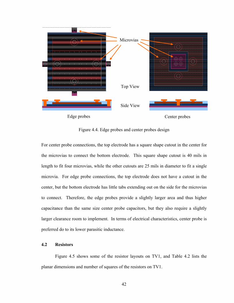
42
Figure 4.4. Edge probes and center probes design
For center probe connections, the top electrode has a square shape cutout in the center for
the microvias to connect the bottom electrode. This square shape cutout is 40 mils in
length to fit four microvias, while the other cutouts are 25 mils in diameter to fit a single
microvia. For edge probe connections, the top electrode does not have a cutout in the
center, but the bottom electrode has little tabs extending out on the side for the microvias
to connect. Therefore, the edge probes provide a slightly larger area and thus higher
capacitance than the same size center probe capacitors, but they also require a slightly
larger clearance room to implement. In terms of electrical characteristics, center probe is
preferred do to its lower parasitic inductance.
4.2 Resistors
Figure 4.5 shows some of the resistor layouts on TV1, and Table 4.2 lists the
planar dimensions and number of squares of the resistors on TV1.
Side View
Edge probes Center probes
Top View
Microvias

43
Figure 4.5. Various geometric shapes and sizes of resistors on TV1
Table 4.2. Dimensions of various embedded resistors on TV1
Width (mil) Length (mil) Number of Corners Number of Squares
10 10 0 1
10 60 4 10
10 90 6 15
10 140 6 20
10 575 36 100
20 20 0 1
20 120 4 10
20 180 6 15
20 280 6 20
20 1130 36 100
30 30 0 1
30 180 4 10
30 270 6 15
30 425 6 20
30 1940 36 100
40 40 0 1
40 240 4 10
40 360 6 15
40 560 6 20
40 2470 38 100

44
As listed in Table 4.2, a wide variety of resistors are designed to evaluate the
processability and reliability of the resistors. These resistors are made of carbon ink
based PTF material from Asahi. Two sheet resistances of 10 Ω/ sq and 10 kΩ/sq are used
to cover the resistance range of 10 Ω – 400 kΩ. Some resistors have same nominal
resistance even though they have different width by maintaining the same number of
squares. Usually, smaller resistors are desired to minimize the PWB footprint area, but
these smaller resistors have less area to dissipate the heat that it generates. If more heat is
generated than it can dissipate, resistors can be permanently damaged.
Similarly, wide variety of resistors is designed for TV2. These resistors are made
of NiCrAlSi thin film foils from Gould Electronics Inc. Three sheet resistances of 25
Ω/sq, 100 Ω/sq, and 250 Ω/sq are used to cover the resistance range of 10 Ω – 100 kΩ.
Figure 4.6 shows some of the resistor layouts on TV2, and Table 4.3 lists the planar
dimensions.
Figure 4.6. Various resistors on TV2

45
Table 4.3. Dimensions of various embedded resistors on TV2
25 Ω / square 100 Ω / square 250 Ω / square
Length (mils)
Width (mils)
Nominal (Ω)
Length (mils)
Width (mils)
Nominal (Ω)
Length (mils)
Width (mils)
Nominal (Ω)
40 10 100 10 10 100 1955 5 97.8K
50 12.5 100 15 15 100 2332 6 97.2K
60 15 100 20 20 100 2695 7 96.3K
10 25 10 100 10 1000 347 10 8.7K
15 37.5 10 120 12 1000 416 12 8.7K
20 50 10 80 8 1000 271 8 8.5K
10 16.7 15 10 13.33 75 120 10 3K
15 25 15 15 20 75 144 12 3K
20 33.3 15 20 26.67 75 96 8 3K
10 12.5 20 188 10 4.7K
15 18.75 20 150.4 8 4.7K
20 25 20 225.6 12 4.7K
15 15.1 24.9 997 5 49.9K
20 20.1 24.9 1193 6 49.7K
25 25.1 24.9 1386 7 49.5K
30 10 75
45 15 75
60 20 75
400 400 25 400 400 100 400 400 250

46
CHAPTER V
FABRICATION OF EMBEDDED PASSIVES
The three main fabricated features for TV1 are capacitors, resistors, and microvias
with probing pads. Figure 5.1 shows some of the clean room equipments that have been
used. For additional details on the fabrication, please refer to Packaging Research Center
at Georgia Institute of Technology [PRC website]. The following sections describe the
sequential build up (SBU) process steps and processing conditions.
Figure 5.1. Clean room equipments
(a) Profilometer (b) Spin Coater (c) Vacuum Laminator
(d) Exposure Tool (e) Electroplating Bath

47
5.1 Capacitor Fabrication Steps and Processing Conditions
Capacitor layer is the first processing step for TV1. This process starts with the
bare core 6-metal layer board with bottom copper electrode already laminated as shown
in Figure 5.2. Figure 5.3 shows the general overview of capacitor fabrication process.
Figure 5.2. Bare board with bottom electrodes and resistor pads

48
Figure 5.3. Overview of capacitor process
• To prepare for the lamination of polymer/ceramic dielectric, the bare board
was first surface treated with acetone to remove any organic residues.
Then, it was microetched to roughen up the surface of bottom copper
electrodes, and bond film was applied to further enhance the adhesion
(Figure 5.3a).
• The polymer/ceramic nanocomposite dielectric was prepared by thoroughly
mixing barium titanate based polymeric resin with hardener and thinner.
The mixture was spin coated onto the bare board to achieve a nominal
thickness of 20 µm. Then, the board was soft cured at 65oC for 45 minutes
(Figure 5.3b).
• For top copper electrode, a 15 µm copper foil was vacuum laminated, and
heat press was performed to strengthen the lamination (Figure 5.3c).
(e) Expose and develop to pattern photoresist
(a) Prepare the bare board with bottom
electrodes
(c) Laminate Cu foil
(b) Spin coat polymer/ceramic
nanocomposite; soft cure
(d) Laminated photoresist
(f) Remove exposed Cu and nanocomposite area,
full cure

49
• Positive acting liquid photoresist Shipley SP20-29 was spin coated onto the
board (Figure 5.3d).
• The top electrode patterns are UV exposed with a positive mask and
developed (Figure 5.3e).
• The resulting exposed copper and nanocomposite materials were removed.
The board is fully cured at 150oC for 1 hour to complete the capacitor
process. This simple and low temperature process exhibited high yield with
specific capacitance of 1.5 nF/cm2 (Figure 5.3f). Figure 5.4 shows the
fabricated capacitors, and Appendix A lists the detailed processing
conditions
Figure 5.4. Pictures of fabricated capacitors
5.2 PTF Resistor Fabrication Steps and Processing Conditions for TV1
Once the capacitor layer is completed, resistor layer was fabricated using a screen
print lift-off process. This process starts with the bare board with resistor copper pads
already attached. Figure 5.5 shows the general overview of resistor fabrication process.

50
Figure 5.5. Overview of resistor process
• The bare board with capacitors already processed was treated with acetone
and microetch solution to thoroughly remove any organic residues and
roughen up the surface to improve the adhesion (Figure 5.5a).
• Negative acting dry film photoresist DuPont RistonTM 4615 was vacuum
laminated. This 30 µm thick photoresist was used to create a deep resist
trace (Figure 5.5b).
• The resist traces are UV exposed with a negative mask and developed
(Figure 5.5c).
• Carbon ink based PTF supplied by W.R. Grace was screen printed into the
developed negative pattern of the resist trace. Both 10 Ω/sq and 10 kΩ/sq
sheet resistances were used (Figure 5.5d).
• The resist materials are soft cured, and the photoresist was stripped.
(c) Expose and develop photoresist
(a) Surface treat core board with Cu/resistor
pads
(b) Laminate photoresist
(d) Apply PTF material, soft cure
(e) Strip photoresist, full
cure

51
• The board was fully cured at 150oC for 1 hour to complete the resistor
process (Figure 5.5e). Figure 5.6 shows the fabricated resistors, and
Appendix B lists the detailed processing conditions.
Figure 5.6. Pictures of fabricated resistors
5.3 Microvia Fabrication Steps and Processing Conditions for TV1
Once the capacitor and resistor layers are completed, microvia was added to
complete the TV1 fabrication. Figure 5.6 shows the general overview of resistor
fabrication process.
• The bare board with capacitors and resistors already processed was treated
with acetone and microetched to thoroughly remove any organic residue
and roughen up the surface to improve adhesion (Figure 5.7a).
• Photo-imageable negative liquid epoxy Vantico Probimer 7081 was spin
coated to achieve a nominal thickness of 30 µm. Once the board was
exposed, it was baked at 100oC for 1 hour to fully crosslink the exposed
photoresist area. GBL solvent at room temperature was used to develop the
unexposed photoresist area, and the board was fully cured at 160oC for 1
hour (Figures 5.7b and 5.7c).

52
Figure 5.7. Overview of microvia and copper probing pad process
• Conventional electroless copper plating was performed to build a thin seed
layer for microvias (Figure 5.7d).
• Conventional photolithography was performed with DuPont Riston 4615
dry film to pattern the probing pads. This photoresist is a 30 µm thick
negative photoresist (Figures 5.7e and 5.7f).
• Copper was electroplated to build the microvias and probing pads (Figure
5.7g). Finally, the photoresist was stripped, and the copper seed layer was
(a) Surface treat core board with Cu/resistor
pads
(b) Laminate liquid epoxy photoresist
(c) Expose and develop via holes,
full cure
(d) Build seed layer by electroless Cu
plating
(e) Laminate photoresist
(f) Expose and develop photoresist,
soft cure
(g) Build exposed area by electroplating Cu
(h) Strip photoresist
(i) Microetch Cu, full cure
… . . . .

53
microetched to complete the process (Figures 5.7h and 5.7i). Figure 5.8
shows the completed TV1, and Appendix C lists the detailed processing
conditions.
Figure 5.8. Picture of completed TV1
5.4 NiCrAlSi Foil Resistor Fabrication Steps and Processing Conditions for TV2
The processing steps and conditions of Gould TCR NiCrAlSi foil resistors were
obtained from Gould Electronics Inc. Figure 5.9 shows the general overview of

54
NiCrAlSi foil resistor fabrication process. The Gould resistor foils contain a sputtered
NiCrAlSi thin film layer on the rough, matte surface of a copper foil. Therefore, the foil
is laminated onto a bare board and two step etching processes are performed. The first
etch solution removes both copper and NiCrAlSi to define the resistors dimensions. The
second etching solution selectively removes the copper. All the fabrication of TV2 was
done at EI Technologies, Inc. Table 5.1 lists the two step etching processes, and Figure
5.10 shows the picture of TV2.
Figure 5.9. Gould resistor fabrication process [Gould website]
(a) Laminate NiCrAlSi resist foil
(b) Laminate photoresist
(c) Expose and develop photoresist
(d) Etch Cu and resistor to define
resistor width
(e) Strip photoresist(f) Laminate photoresist
(g) Etch Cu to define resistor
length
(g) Strip photoresist

55
Table 5.1. NiCrAlSi Etching process
Figure 5.10. Picture of completed TV2
First etch process (removes both copper and resist,
(Figure 5.9d)
Cupric Chloride solution: 200 g/l CuCl2
60 g/l HCl at 52oC
Second etch process (removes copper only, Figure 5.9g)
267 g/l NH4Cl 1 g/l ortho-phosphoric acid
392 ml NH4OH 10 g/l CuCl2 at 54 – 60oC

56
CHAPTER VI
CHARACTERIZATION OF RESISTORS AND
CAPACITORS
6.1 Ideal Capacitor
Usually, the electrical characteristic of storing charge is dominated in a capacitor
that it acts as a capacitor. However, a capacitor also has some resistance and inductance
as parasitic known as Equivalent Series Resistance (ESR) and Equivalent Series
Inductance (ESL). ESR exists due to intrinsic resistance present in the conducting plates
and other leads, and ESL exists due to inductance associated with the parallel plates and
leads. For most capacitor electrodes that are made of copper or aluminum, ESR is
negligible. However, if the plates are very thin or if they are made of valve or refractory
metals, then ESR should be considered more seriously. ESL is dependent on the
frequency at which the capacitor operates. As shown in Figure 6.1, the capacitor
impedance increases as frequency increases.
Simplified Ideal Passive Impedance
0.001 0.01 0.1 1 10
Arbitrary frequency (GHz)
Impe
danc
e le
vel
R Impedance L Impedance C Impedance
Figure 6.1. Frequency dependent ideal passive impedance

57
At a certain frequency known as resonant frequency, the inductive characteristic becomes
more dominant, and the capacitor no longer acts as capacitor but as an inductor. This
marks the upper limit of the useful frequency range of a capacitor.
In comparison to surface mount counterparts, embedded capacitor has typically
two orders of magnitude smaller parasitic inductance. The two main reasons are: 1)
smaller current loop and 2) reduction in self-inductance by mutual inductance. Surface
mounts have much larger current loop, as the current has to travel above the surface
through the leads. This advantage due to smaller current loop makes embedded
capacitors more attractive in high frequency applications.
6.2 High Frequency Measurement
The high frequency performance of TV1 440 mils circular capacitor was
measured with Vector Network Analyzer (VNA) and two Ground-Signal (G-S) probes as
shown in Figure 6.2. This equipment is capable of measuring high frequency up to 3
GHz. The pitch of the probes is 500 µm, and the locations of probes with respect to a
capacitor are shown in Figure 6.3.
Figure 6.2. Vector Network Analyzer setup

58
Figure 6.3. Ground and signal probe locations
As shown in Figure 6.3, the ground probes are connected to the bottom electrodes, and
the two signal probes are connected to the top electrodes. The types and locations of
probes can cause significant inductance in the measurements [Chen et al., 2000]. In order
to minimize any parasitic from the connection, these probes are located closely together
to minimize the loop inductance. Also, two-port measurement was performed to
minimize the chance of loose connections. The calibration of the equipment was based
on commonly used Short-Open-Load-Thru (SOLT) calibration technique [Cascade
Microtech website]. Entire calibration and actual measurements were performed by the
research engineers at PRC. The measurement results are shown in Figures 6.4 and 6.5.
Figure 6.4. Extracted capacitance of the structure.
S1 G1 G2 S2

59
Figure 6.5. Impedance profile of the capacitor.
Figure 6.4 shows the impedance measurement with respect to frequency. Frequency
range of 50 MHz – 2 GHz was scanned, and the capacitor resonates at around 900 MHz.
Figure 6.5 shows the measurement of capacitance with respect to frequency. Capacitance
essentially remains steady during the frequency range of 200 MHz to 1.8 GHz.
6.3 Temperature Coefficient of Resistance and Capacitance
The TCR and TCC measure change in resistance and capacitance with respect to
change in temperature as previously discussed in section 2.4. It is important to
understand how these parameters affect the resistivity or capacitance to minimize any
undesirable changes.
The TCR of PTF material and TCC of nanocomposite dielectric were measured
by using a hot plate and a thermocouple. The measurement was performed while the
temperature was varied between approximately 25oC to 125oC. Figure 6.6 shows the
measurement setup.

60
Figure 6.6. TCR and TCC measurement setup
As shown above in Figure 6.6, the measurement setup consists of various equipments
including LCR meter, microscope, thermocouple, insulator, and weights. First, a
thermocouple and insulation materials are mounted near the component on top of the
board to accurately measure the component temperature. This board is then placed on
top of the heat plate to heat up the board. Before the heat plate is activated, two LCR
probes are aligned with the microvia pads using the microscope. Also, several weights
Temperature sensor
Microscope for alignment
LCR meter
Insulator Weights
Probes
Thermocouples
Hot plate

61
are placed around the board to prevent it from warpage and secure firm contact of probes
with the pads.
Once the setup is completed, the board is heated to approximately 125oC and
maintained at the high temperature. Then, the heat plate is turned off, and while the
entire setup is cooling down by natural ambient air, resistance or capacitance is
incrementally measured. The measurements are taken while it is cooling instead of
heating since it is difficult to control the heating rate. Also since TCR and TCC are based
on their intrinsic material properties, components with the highest respective material
volume percentage such as resistors with 100 square and 40 mil width or capacitors with
440 mil diameter were measured. Several measurements were completed as shown in
Figures 6.7 and 6.8, and Table 6.1 summarizes the results.
Temperature Coefficient of Resistance
Case 2y = 0.1633x + 516.29
R2 = 0.9928
Case 3y = 0.1595x + 516.35
R2 = 0.9936
Case 1 y = 0.1868x + 453
R2 = 0.9976
450
480
510
540
570
0 50 100 150
Temperature (C)
Res
ista
nce
(ohm
s)
Case 1
Cases 2 and 3
Figure 6.7. TCR measurements

62
Temperature Coefficient of Capacitance
Case 2y = 0.0024x + 1.2886
R2 = 0.9993
Case 3y = 0.0023x + 1.2903
R2 = 0.9993
Case 1y = 0.0013x + 1.0059
R2 = 0.9993
0.4
0.8
1.2
1.6
2
0 20 40 60 80 100 120 140
Temperature (C)
Cap
acita
nce
(nF)
Cases 2 and 3
Case 1
Figure 6.8. TCC measurements
Table 6.1 Summary of TCR and TCC measurement
Both Figures 6.7 and 6.8 show linear relationship between the resistance and capacitance
with respect to temperature. Since TCR and TCC are based on the material property, all
the measurements should have similar results. Although Cases 2 and 3 share similar
results, Case 1 is slightly different from others possibly due to localized degradation of
material or simple measurement errors. Measurements of Cases 2 and 3 are performed
within few hours apart and they were based on a same component; however, Case 1 was
TCR Test Cases TCR (ppm/oC) TCC Test Cases TCC (ppm/oC)
Case 1 (100 sq/40 mil width PTF) 407 Case 1
(440 mil circular) 1244
Case 2 (100 sq/40 mil width PTF) 313 Case 2
(440 mil circular) 1790
Case 3 (100 sq/40 mil width PTF) 306 Case 3
(440 mil circular) 1715

63
tested few days prior to other measurements and it was based on a different component.
In terms of the magnitude of TCR and TCC, they are higher than desired, but they are
expected. PTF material is known for its difficulty in achieving stability with respect to
temperature. Also, capacitor nanocomposite, which is a mixture of barium titanate based
ferroelectric ceramic particles in organic material, could lead to unstable electrical
characteristics. High TCC is expected when barium titanate has high TCC of ~5000
ppm/oC and epoxy has TCC of ~300 ppm/oC.
6.4 Warpage Measurement using Shadow Moiré
Shadow moiré interferometry is a well established technique that can accurately
measure the out-of-plane displacement or warpage of a test sample [Hassell, 2001]. It
analyzes the fringes that are created from the interference between the equally spaced
reference grating and the shadows of grating reflected on the test sample. Figure 6.9
shows a simplified experimental setup.
Figure 6.9. Simplified shadow moiré experiment setup
Light source at 45o
Reference grating
Test sample Oven
Camera

64
As shown above in Figure 6.9, light is projected onto the reference grating, which creates
shadow of gratings. If the test sample is not flat, then the grating and its shadow create
fringe patterns that can be analyzed by Equation 6.1.
βα tantan +
=Npz (Eq. 6.1)
z is the out-of-plane displacement, Np is the number of fringes, α is the illumination
angle, and β is the observation angle.
Shadow moiré interferometry was performed to measure the warpage of TV1.
The fringe patterns were captured at various temperatures approximately from 30oC to
150oC. The measurements were based on grating resolution of 100 lines per inch. Figure
6.10 shows warpage measurement results.
As shown in Figure 6.10, TV1 is initially warped in a saddle shape, and as the
temperature rises from 25oC to 150oC, it gradually warps into a spherical shape. Highest
warpage resulted at 150oC with 1.68 mm out-of-plane displacement. The direction of
warpage is expected since there is higher volume of substrate dielectric, which has
highest CTE, on the bottom of the test board. As the entire board heats up, bottom half of
the board expands more than the top half.

65
Figure 6.10. Warpage measurements at different temperatures
(a) Warpage at 25oC = 1.48 mm (b) Warpage at 60oC = 1.24 mm
(c) Warpage at 90oC = 1.07 mm (d) Warpage at 150oC = 1.68 mm

66
CHAPTER VII
EXPERIMENTAL RELIABILITY ASSESSMENT
Although embedded passives present better reliability with the elimination of
solder joint interconnects, the embedded passives also introduce other concerns such as
cracks, delamination and component instability. More substrate layers will be needed to
accommodate the embedded passives, and various materials within the substrate may
cause significant thermo-mechanical stress due to CTE mismatch. Unlike surface
mounted components where defective parts can be reworked and replaced, a single bad
component can obliterate the entire board. Consequently, reliability is a major issue in
the acceptance and success of embedded passives technology.
EI Technologies, Inc. has fabricated both TV1 and TV2 in bulk, and these test
boards are used for all the reliability tests. These test boards from EI Technologies, Inc.
share the same board layers described in earlier chapters. However, some material
discrepancies exist due to material availability. All the resistor materials are identical,
but the dielectric material used in the microvia layer is Dynavia 2000TM instead of
Vantico Probimer 7081TM. These materials have similar electrical properties and
processing conditions.
7.1 Reliability Qualification Test Conditions and Equipments
Instead of a typical field use condition, reliability qualification tests are performed
under a more demanding environment to accelerate the failure mechanisms, namely,
temperature, humidity, voltage, and pressure. Four reliability qualification tests based on

67
JEDEC and MIL standards were used to evaluate the embedded passives as listed in
Table 7.1.
Table 7.1. Reliability qualification test conditions
All thermal cycling tests were performed with Thermotron ATS-320-DD
chamber. It consists of three chambers stacked together vertically as shown in Figure
7.1. The top and bottom chambers were maintained at constant temperature of 125oC,
and the middle chamber was maintained at -40 or -55oC. Two large baskets inside these
chambers hold the test samples, and as the baskets move up and down, the test samples
are exposed to two extreme temperatures. The dwell time in each temperature extreme
was 10 minutes; hence, each cycle was 20 minutes long. After every 100 or 200 cycles
of continuous run, the test vehicles were removed from the chambers for electrical
measurements. These tests were conducted for 1000 cycles.
Test Cases Test Conditions Test Duration
Air to Air Thermal Cycling -40 – 125oC
Each cycle consists of 10 minute dwell at each extreme temperature,
20 minutes per cycle, Total of 1000 cycles
Air to Air Thermal Cycling -55 – 125oC
Each cycle consists of 10 minute dwell at each extreme temperature,
20 minutes per cycle, Total of 1000 cycles
Steady State Temperature
Humidity Test 85oC / 85 RH 1000 hours
Highly Accelerated Stress Test (HAST) 121oC / 100 RH 96 hours

68
Figure 7.1. Schematics of thermal chamber
Steady state temperature and humidity tests and HAST were performed with
Thermotron 2800 and ESPEC HAST System TPC-422M as shown in Figure 7.2
respectively. After every 100 hours of continuous run, the test vehicles were removed
from the chamber for electrical measurements. Steady state test and HAST were
conducted for 1000 hours and 96 hours respectively.
Figure 7.2. Humidity test chambers
(a) Steady state temperature and humidity
chamber (b) HAST chamber
Basket 1
Basket 2
Hot 125oC
Hot 125oC
Cold -55 or -40oC

69
7.2 Test Results of Test Vehicle 1
For each test vehicles, different conditions of air-to-air thermal cycling and
constant temperature and humidity tests were performed. The test results are divided into
three sections:
1. TV1 PTF Resistors
2. TV1 Capacitors
3. TV2 NiCrAlSi Thin Film Foil Resistors
For TV1, three different configurations of TV1 designs were fabricated and
tested: resistors only, capacitors only, and resistors and capacitors together. Although
the original TV1 design included both resistors and capacitors, some test boards were
fabricated with just one type of component and not the other. This separation removes
possible interaction between the processing conditions. Other differences between these
boards are sheet resistance of resistors.
Resistors are described by three design parameters: sheet resistances, number of
squares, and width of squares. Sheet resistances represent the different material
properties, and the number of squares and width of square represent the planar
dimensions. The effects of these three categories on the resistor reliability are presented.
For capacitors, effects of design parameters including planar dimensions, geometric
shapes, and microvia locations on the reliability are presented. Also, changes in Q-
Factors are compared against capacitor shapes and sizes.
7.2.1 Reliability Test Results for Test Vehicle 1 PTF Resistors
Four unique test cases for TV1 PTF resistors are depicted in Table 7.2.
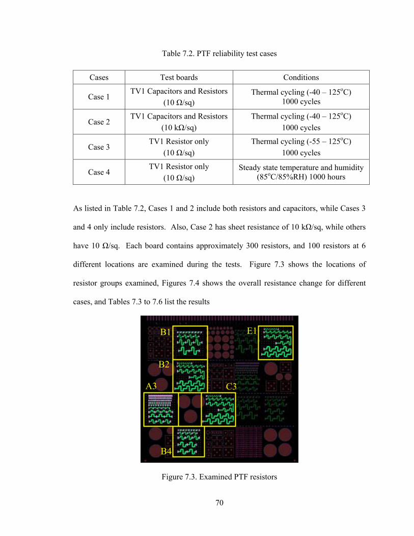
70
Table 7.2. PTF reliability test cases
As listed in Table 7.2, Cases 1 and 2 include both resistors and capacitors, while Cases 3
and 4 only include resistors. Also, Case 2 has sheet resistance of 10 kΩ/sq, while others
have 10 Ω/sq. Each board contains approximately 300 resistors, and 100 resistors at 6
different locations are examined during the tests. Figure 7.3 shows the locations of
resistor groups examined, Figures 7.4 shows the overall resistance change for different
cases, and Tables 7.3 to 7.6 list the results
Figure 7.3. Examined PTF resistors
Cases Test boards Conditions
Case 1 TV1 Capacitors and Resistors
(10 Ω/sq) Thermal cycling (-40 – 125oC)
1000 cycles
Case 2 TV1 Capacitors and Resistors
(10 kΩ/sq) Thermal cycling (-40 – 125oC)
1000 cycles
Case 3 TV1 Resistor only
(10 Ω/sq) Thermal cycling (-55 – 125oC)
1000 cycles
Case 4 TV1 Resistor only
(10 Ω/sq) Steady state temperature and humidity
(85oC/85%RH) 1000 hours
B2
B1 E1
A3 C3
B4
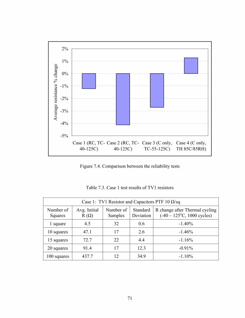
71
-5%
-4%
-3%
-2%
-1%
0%
1%
2%
Case 1 (RC, TC-40-125C)
Case 2 (RC, TC-40-125C)
Case 3 (C only,TC-55-125C)
Case 4 (C only,TH 85C/85RH)
Ave
rage
resi
stan
ce %
cha
nge
Figure 7.4. Comparison between the reliability tests
Table 7.3. Case 1 test results of TV1 resistors
Case 1: TV1 Resistor and Capacitors PTF 10 Ω/sq
Number of Squares
Avg. Initial R (Ω)
Number of Samples
Standard Deviation
R change after Thermal cycling (-40 – 125oC, 1000 cycles)
1 square 4.5 32 0.6 -1.40%
10 squares 47.1 17 2.6 -1.46%
15 squares 72.7 22 4.4 -1.16%
20 squares 91.4 17 12.3 -0.91%
100 squares 437.7 12 34.9 -1.10%

72
Table 7.4. Case 2 test results of TV1 resistors
Table 7.5. Case 3 test results of TV1 resistors
Table 7.6. Case 4 test results of TV1 resistors
Case 2: TV1 Resistor and Capacitors PTF 10 kΩ/sq
Number of Squares
Avg. Initial R (kΩ)
Number of Samples
Standard Deviation
R change after Thermal cycling (-40 – 125oC, 1000 cycles)
1 square 4.8 32 0.1 -3.36%
10 squares 38.5 17 1.4 -4.32%
15 squares 57.9 22 2.5 -4.19%
20 squares 80.3 17 2.0 -4.29%
100 squares 374.2 12 27.7 -4.43%
Case 3: TV1 Resistor only – PTF 10 Ω/sq
Number of Squares
Avg. Initial R (kΩ)
Number of Samples
Standard Deviation
R change after Thermal cycling (-40 – 125oC, 1000 cycles)
1 square 7.8 25 1.0 -4.75%
10 squares 55.6 15 7.8 -2.63%
15 squares 86.1 22 19.5 -2.19%
20 squares 110.8 17 17.9 -2.07%
100 squares 503.3 12 71.8 -1.98%
Case 4: TV1 Resistor only – PTF 10 Ω/sq
Number of Squares
Avg. Initial R (kΩ)
Number of Samples
Standard Deviation
R change after Thermal cycling (-40 – 125oC, 1000 cycles)
1 square 6.3 32 0.4 1.70%
10 squares 51.6 17 5.4 1.30%
15 squares 76.2 22 11.5 1.35%
20 squares 100.8 17 13.5 1.04%
100 squares 445.4 12 26.7 1.00%

73
Before the changes in resistances are averaged, each resistor value is normalized
to make each resistor count equally. After 1000 thermal cycles, all resistors experienced
a slight decrease in the resistance, whereas after 1000 hours of constant temperature and
humidity test, all the resistors experienced a slight increase in the resistance. Although
Damani [Damani, 2004] has reported similar decrease in the resistance after thermal
cycling, this result is unexpected. The degradation of resistor material due to thermo-
mechanical loads should increase the resistance. The decrease in the resistance is most
likely due to presence of partially cured resistors. As they are thermal cycled, the PTF
materials continue to cure, which shrinks and compacts the resist materials to yield lower
resistance. This explanation is supported by the plot of resistance change over cycles as
shown in Figure 7.5.
Thermal Cycled 10 ohms/sq Resistors
-10%
-8%
-6%
-4%
-2%
0%
0 200 400 600 800 1000
Cycles
Ave
rage
resi
stan
ce %
cha
nge
1 sq 10 sq 15 sq 20 sq 100 sq
Figure 7.5. Resistance change during thermal cycling

74
As shown in Figure 7.5, there is a sharp decrease in the resistance during the first 200
cycles. Then, the resistances gradually increase and stabilize. This sequence indicates
that the materials were still being cured during the first 200 cycles. After this curing,
further thermal cycling results in degradation of the material properties; and therefore, the
resistance increases by about 4% from the resistance of the fully cured material.
The increase of the resistance by about 2% during the humidity test is expected.
The absorbed moisture expands the entire board, and the resistors are stressed and
deformed.
Effect of Planar Dimensions and Resistor Location on Resistance Change
In terms of number of squares or width of squares, there seem to be a no clear
trend on which configuration performs better as shown in Figures 7.6 and 7.7. The
percentage change in the resistance remains the same regardless of the planar dimensions.
It should be pointed out that when only one square is used for measurements, there
appears to be a deviation in the results. This is possibly due to the fact that the averaging
effects of multiple squares are not considered when one square is used for the
measurement.
Similar to planar dimensions, the percentage in the resistance remains same
regardless of the location of resistors. Figure 7.8 compares three groups of identical
resistors at different locations of B2, C3, and E1.

75
-6%
-4%
-2%
0%
2%
4%
Case 1 (RC,TC-40-125C)
Case 2 (RC,TC-40-125C)
Case 3 (C only,TC-55-125C)
Case 4 (C only,TH 85C/85RH)
Ave
rage
resi
stan
ce %
cha
nge
1 sq 10 sq 15 sq 20 sq 100 sq
Figure 7.6. Comparison of resistors in terms of number of squares
-6%
-4%
-2%
0%
2%
4%
Case 1 (RC,TC-40-125C)
Case 2 (RC,TC-40-125C)
Case 3 (C only,TC-55-125C)
Case 4 (C only,TH 85C/85RH)
Ave
rage
resi
stan
ce %
cha
nge
10 mil 20 mil 30 mil 40 mil
Figure 7.7. Comparison of resistors in terms of width of squares

76
-6%
-4%
-2%
0%
2%
Case 1 (RC, TC-40-125C)
Case 2 (RC, TC-40-125C)
Case 3 (C only,TC-55-125C)
Case 4 (C only,TH 85C/85RH)
Ave
rage
resi
stan
ce %
cha
nge
B2 C3 E1
Figure 7.8. Comparison of resistor locations
All the reliability qualification tests showed that PTF resistors are quite reliable.
None of the resistors failed during the tests, and the average resistance changes are within
5%. The sheet resistance had most effect on the resistance change compared to the planar
dimensions or locations of resistors. This could be due to different thermo-mechanical
properties between the materials. 10 kΩ/sq resistors could have higher CTE mismatch
than 10 Ω/sq resistors that more severe thermo-mechanical deformation could have
occurred.
7.2.2 Test Results of Test Vehicle 1 Capacitor
Four test cases for TV1 capacitors are depicted in Table 7.7.

77
Table 7.7. Capacitor reliability test cases
As listed in Table 7.7, Cases 1 and 2 include both resistors and capacitors, while Cases 3
and 4 only include capacitors. The difference between the Cases 1 and 2 is that they have
different resistor material. This should not have any effect on the capacitors, and
therefore, these boards should yield similar results. Within each board, 68 of 98 total
capacitors are strategically selected to represent various geometric shapes and planar
dimensions. For each capacitor, both capacitance and Q-Factor are measured at a low
frequency of 100 kHz. Figure 7.9 shows the locations of capacitor group examined,
Figure 7.10 plots the overall results, and Tables 7.8 to 7.15 summarize the results.
Cases Test boards Conditions
Case 1 TV1 Capacitors and Resistors (10 Ω/sq)
Thermal cycling (-40 – 125oC) 1000 cycles
Case 2 TV1 Capacitors and Resistors (10 kΩ/sq)
Thermal cycling (-40 – 125oC) 1000 cycles
Case 3 TV1 Capacitors only (10 Ω/sq)
Thermal cycling (-55 – 125oC) 1000 cycles
Case 4 TV1 Capacitors only (10 Ω/sq)
Steady state temperature and humidity (85oC/85%RH) 1000 hours

78
Figure 7.9. Examined capacitors
-20%
-15%
-10%
-5%
0%
5%
10%
15%
20%
Case 1 (RC, TC-40-125C)
Case 2 (RC, TC-40-125C)
Case 3 (C only,TC-55-125C)
Case 4 (C only,TH 85C/85RH)
Ave
rage
cap
acita
nce
% c
hang
e
Figure 7.10. Reliability test results of capacitors
C1
B3
C2
A4 C4

79
Table 7.8. Case 1: capacitance results of TV1 capacitors
Table 7.9. Case 2: capacitance results of TV1 capacitors
Case 1: Thermal Shock (-40 to 125oC 1000 cycles)
Capacitor Shape Size
(diameter or length in mil)
Average Initial Capacitance at 100 kHz (pF)
Number of Samples
Standard Deviation
Average % Change
Circular edge 110 63 5 7.5 -2.92%
Circular center 145 73 10 10.8 -2.67%
Circular center 240 269 10 40.2 -2.20%
Circular center 440 1050 5 177.8 -1.79%
Square edge 110 58 4 17.6 -3.08%
Square center 110 42 6 6.8 -3.20%
Square edge 160 217 7 51.1 -1.96%
Square center 160 164 9 26.7 -2.11%
Square center 360 997 5 141.2 -1.90%
Case 2: Thermal Shock (-40 to 125oC 1000 cycles)
Capacitor Shape Size
(diameter or length in mil)
Average Initial Capacitance at 100 kHz (pF)
Number of Samples
Standard Deviation
Average % Change
Circular edge 110 88 5 3.2 -2.71%
Circular center 145 127 7 14.6 -2.59%
Circular center 240 357 10 58 -2.62%
Circular center 440 1188 5 115.2 -1.92%
Square edge 110 83 3 18.3 -3.31%
Square center 110 65 5 3.9 -2.85%
Square edge 160 306 8 66.7 -2.86%
Square center 160 185 10 22.9 -2.83%
Square center 360 1043 3 85.5 -2.18%
80
Table 7.10. Case 3: capacitance results of TV1 capacitors
Table 7.11. Case 4: capacitance results of TV1 capacitors
Case 3: Thermal Shock (-55 to 125oC 1000 cycles)
Capacitor Group
Size (diameter or
length in mil)
Average Initial Capacitance at 100 kHz (pF)
Number of Samples
Standard Deviation
Average % Change
Circular edge 110 45 7 1.6 -26.44%
Circular center 145 61 10 2.4 -20.22%
Circular center 240 149 10 18.7 -8.88%
Circular center 440 613 5 33.2 -2.09%
Square edge 110 52 4 2.9 -22.42%
Square center 110 46 6 2.9 -26.15%
Square edge 160 90 8 7.7 -11.79%
Square center 160 94 10 5.6 -14.63%
Square center 360 432 8 25.9 -3.50%
Case 4: Constant Temperature Humidity (85oC/85%RH 1000 hours)
Capacitor Group Size
(diameter or length in mil)
Average Initial Capacitance at 100 kHz (pF)
Number of Samples
Standard Deviation
Average % Change
Circular edge 110 30 7 2.2 19.68%
Circular center 145 46 10 2.7 13.89%
Circular center 240 131 10 20.4 12.52%
Circular center 440 534 5 36.6 9.87%
Square edge 110 37 1 NA 16.85%
Square center 110 28 6 2.0 16.72%
Square edge 160 NA NA NA NA
Square center 160 74 10 8.6 12.39%
Square center 360 358 8 27.8 9.87%

81
Table 7.12. Case 1: Q-Factor results of TV1 capacitors
Table 7.13. Case 2: Q-Factor results of TV1 capacitors
Case 1: Thermal Shock (-40 to 125oC 1000 cycles)
Capacitor Shape Size
(diameter or length in mil)
Average Initial Q-Factor at 100
kHz
Number of Samples
Standard Deviation
Average % Change
Circular edge 110 44 5 2.6 27.98%
Circular center 145 44 10 0.9 26.89%
Circular center 240 46 10 7.3 49.83%
Circular center 440 52 5 1.3 52.49%
Square edge 110 43 4 0.8 29.65%
Square center 110 42 6 0 23.02%
Square edge 160 48 7 2.9 34.93%
Square center 160 45 9 1.4 27.48%
Square center 360 51 5 1.1 42.02%
Case 2: Thermal Shock (-40 to 125oC 1000 cycles)
Capacitor Shape Size
(diameter or length in mil)
Average Initial Q-Factor at 100
kHz
Number of Samples
Standard Deviation
Average % Change
Circular edge 110 41 5 0 22.57%
Circular center 145 40 7 0.7 22.04%
Circular center 240 46 10 1.0 34.94%
Circular center 440 50 5 2.5 43.78%
Square edge 110 40 3 0.6 24.79%
Square center 110 39 5 0 17.52%
Square edge 160 46 8 1.1 33.24%
Square center 160 41 10 1.7 23.79%
Square center 360 48 3 1.5 33.79%

82
Table 7.14. Case 3: Q-Factor results of TV1 capacitors
Table 7.15. Case 4: Q-Factor results of TV1 capacitors
Case 3: Thermal Shock (-55 to 125oC 1000 cycles)
Capacitor Group
Size (diameter or
length in mil)
Average Initial Q-Factor at 100
kHz
Number of Samples
Standard Deviation
Average % Change
Circular edge 110 37 7 1.3 104.96%
Circular center 145 38 10 0.8 102.13%
Circular center 240 45 10 1.7 65.17%
Circular center 440 61 5 0.8 42.48%
Square edge 110 39 4 1.0 92.36%
Square center 110 36 6 2.0 103.21%
Square edge 160 44 8 2.0 72.86%
Square center 160 43 10 1.7 75.93%
Square center 360 55 8 0.8 49.77%
Case 4: Constant Temperature Humidity (85oC/85%RH 1000 hours)
Capacitor Group Size
(diameter or length in mil)
Average Initial Q-Factor at 100
kHz
Number of Samples
Standard Deviation
Average % Change
Circular edge 110 57 7 1.0 -47.24%
Circular center 145 54 10 0.6 -41.92%
Circular center 240 54 10 0.5 -40.93%
Circular center 440 66 5 0.8 -46.21%
Square edge 110 50 1 1.4 -39.22%
Square center 110 51 6 0.5 -41.25%
Square edge 160 53 NA NA NA
Square center 160 52 10 0.6 -39.11%
Square center 360 58 8 0.5 -41.42%

83
Once again, each capacitor is normalized and then averaged to make each
capacitor count equally. After 1000 thermal cycle, all the capacitor groups experienced
decrease in the capacitance. This trend is expected, since thermal loads degrade the
dielectric material resulting in decrease in the dielectric constant. Also, thermo-
mechanical deformation could cause the parallel plate electrodes to delaminate and
thickness to increase. The test board that was cycled between -55 to 125oC shows much
higher capacitance percent change than the boards that were cycled between -40 to
125oC. Although this trend is expected, the magnitude of differences is much higher than
expected. Also, Cases 1 and 2 which had different resistor materials but shared same
thermal cycling condition have similar results as expected. This suggests that the resistor
materials do not affect or interact with the capacitor layer.
After 1000 hours of constant temperature and humidity test, capacitors
experienced increase of 10% to 20% in capacitance. This increasing trend is expected,
since absorbed moisture has higher dielectric constant.
Effect of Geometric Shapes and Planar Dimensions on Capacitance Change
For each test conditions, capacitors are separated into seven different
combinations of planar dimensions and geometric shapes as shown in Figure 7.11.
Although size of capacitors in Cases 1 and 2 does not seem to affect the capacitance
change, there is a clear trend of smaller capacitor having higher average percentage
change in Cases 3 and 4.
This result suggests that the dimension of capacitor plays a critical role in the
overall reliability. Especially in cases 3 and 4, noticeable difference in the capacitance
change suggest that the change could be a stronger function of thermo-mechanical
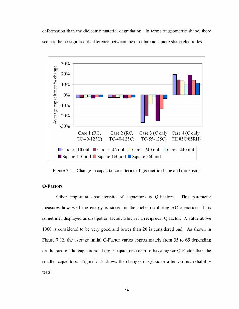
84
deformation than the dielectric material degradation. In terms of geometric shape, there
seem to be no significant difference between the circular and square shape electrodes.
-30%
-20%
-10%
0%
10%
20%
30%
Case 1 (RC,TC-40-125C)
Case 2 (RC,TC-40-125C)
Case 3 (C only,TC-55-125C)
Case 4 (C only,TH 85C/85RH)
Ave
rage
cap
acita
nce
% c
hang
e
Circle 110 mil Circle 145 mil Circle 240 mil Circle 440 milSquare 110 mil Square 160 mil Square 360 mil
Figure 7.11. Change in capacitance in terms of geometric shape and dimension
Q-Factors
Other important characteristic of capacitors is Q-Factors. This parameter
measures how well the energy is stored in the dielectric during AC operation. It is
sometimes displayed as dissipation factor, which is a reciprocal Q-factor. A value above
1000 is considered to be very good and lower than 20 is considered bad. As shown in
Figure 7.12, the average initial Q-Factor varies approximately from 35 to 65 depending
on the size of the capacitors. Larger capacitors seem to have higher Q-Factor than the
smaller capacitors. Figure 7.13 shows the changes in Q-Factor after various reliability
tests.

85
0
10
20
30
40
50
60
70
Qua
lity
Fact
or
Circle 110 mil Circle 145 mil Circle 240 mil Circle 440 milSquare 110 mil Square 160 mil Square 360 mil
Figure 7.12. Averaged initial Q-Factor
-60%
-30%
0%
30%
60%
90%
120%
Case 1 (RC,TC-40-125C)
Case 2 (RC,TC-40-125C)
Case 3 (C only,TC-55-125C)
Case 4 (C only,TH 85C/85RH)
Ave
rage
Q-F
acto
r % c
hang
e
Circle 110 mil Circle 145 mil Circle 240 mil Circle 440 milSquare 110 mil Square 160 mil Square 360 mil
Figure 7.13. Change in Q-Factor of capacitors.
As shown in Figure 7.13, Q-Factors increased after thermal cycling. This increasing
trend suggests that the dielectric material is storing energy better after the thermal
cycling. One possible explanation for such unexpected results is that the dielectric was

86
not fully cured. As the thermal cycling gradually cures the dielectric, the performance of
capacitor is improved. After steady state temperature and humidity test, all types of
capacitors experienced increased in Q-Factor of about 40%. This is due to increased
moisture absorption.
The reliability qualification tests show that there is room for currently used
embedded capacitor process to improve. Although Cases 1 and 2 showed less than 5%
change in capacitance, significant change of approximately 20% are observed in Cases 3
and 4. This drastic difference is difficult to explain. The main difference between these
cases is that Cases 3 and 4 do not contain any resistors. Although absence of resistor
layer should have simplified the process steps, the different processing condition must
have affected the final test boards.
7.3 Test Results of Test Vehicle 2 NiCrAlSi Resistors
Four identical TV2s with NiCrAlSi thin film foil resistors were tested at two
different conditions.
• Air to air thermal cycling (-55 to 125oC) for 1000 cycles
• Highly Accelerated Stress Test (121oC/100RH) for 96 hours
Each TV2 contained approximately 550 resistors, and 100 resistors were monitored
during the tests. Overall, NiCrAlSi resistors showed much more stable results than the
PTF resistors. All four tests showed less than 1% increase in resistance. Among all the
resistors examined, however, one resistor that was thermal cycled became open. Figure
7.14 shows the locations of resistor groups examined, Figure 7.15 shows the resistance
change, and Table 7.16 summarizes the results.

87
Figure 7.14. Examined NiCrAlSi resistors
0.0%
1.0%
2.0%
3.0%
4.0%
5.0%
Board 1 (TC -55-125C)
Board 2 (TC -55-125C)
Board 3 (HAST121C/100%RH)
Board 4 (HAST121C/100%RH)
Ave
rage
resi
stan
ce %
cha
nge
Figure 7.15. NiCrAlSi resistor test results
T1 T21 T3 T4 T5 T6
M1 M2 M3
B1 B1 B3
B2 B2 B4

88
Table 7.16. Summary of NiCrAlSi resistance change
7.4 Cross-Sectioning of Test Vehicles
After completion of various qualification tests, test boards were cross-sectioned to
visually investigate the causes of change in resistance and capacitance. Figures 7.16 and
7.17 show the cross-sections of resistors and capacitors.
NiCrAlSi foil
Resistor group
Resistance range (Ω)
Thermal cycle (-55 to 125oC 1000 cycles)
HAST (121oC/ 100RH
100 hours)
T1 ~ 20 0.43% 0.38%
T2 ~ 100 0.07% 0.08%
T3 ~ 75 0.06% 0.05%
T4 ~ 1 k 0.04% 0.09%
T5 ~ 3 k 0.38% 0.84%
T6 ~ 9 k 0.41% 0.69%
M1 20 – 100 0.21% 0.07%
M2 70 – 100 0.06% 0.08%
M3 ~9 k 0.30% 0.70%
B1 ~ 60 k 0.31% 0.52%
B2 ~ 100 k 0.30% 0.53%
B3 5 – 10 0.51% 0.68%
B4 ~ 15 0.07% 0.72%

89
Figure 7.16. Cross-sections of resistors in TV1
(c) 10 Ω after humidity test (1000 hours)
(a) 10 Ω after thermal cycle (1000 cycles)
(b) 10 kΩ after thermal cycle (1000 cycles)
Dielectric
Resistor
Substrate
20 µm
20 µm
20 µm
Dielectric
Resistor
Substrate
Dielectric
Resistor
Substrate

90
Figure 7.17. Cross-sections of capacitors in TV1
(c) Capacitor only test board after humidity test (1000 hours)
(b) Capacitor only test board after thermal cycling (1000 cycles)
(a) Capacitor and resistor test board after thermal cycling (1000 cycles)
0.2 mm
Microvia
Bottom electrode
Top electrode
Substrate
0.2 mm
0.2 mm

91
Figure 7.16 shows the cross-sections of three test cases of TV1 resistors. All cases show
no visible sign of cracking or delamination within the resistor layers. Also, all cases
show similar thickness of resistors, but 10 kΩ resistor in Figure 7.16b is noticeably darker
than 10 Ω resistors. Figure 7.17 shows cross-sections of three test cases of TV1
capacitors. All figures shows edge probed capacitors with microvias. Although there is
no visible sign of cracking or delamination, some microvias are severely deformed. Also,
there is a dramatic difference in the capacitor dielectric thickness between the figures,
which explains the wide range of capacitance between the test boards. Table 7.17
compares the thicknesses of capacitor dielectric and their averaged initial capacitance
between the test cases.
Table 7.17 Wide range of initial capacitance due to different dielectric thicknesses
Initial Capacitance (pF)
Test cases Thickness (µm)
Square Edge
2.8 mm
Square Center 2.8 mm
Square Edge 4 mm
Square Center 4 mm
Case 1 R and C board Thermal cycled
~15 58 42 217 164
Case 2 R and C board Thermal cycled
~10 83 65 306 185
Case 3 C only board
Thermal cycled ~ 30 – 40 52 46 90 94
Case 4 C only board
Humidity ~25 – 35 37 28 NA 74

92
As shown above in Table 7.17, thicknesses vary from approximately 10 µm to 40 µm.
This high variation resulted in a wide range of average initial capacitance from 74 pF to
306 pF for 4 mm capacitors.
Among 400 NiCrAlSi resistors tested, one of the resistors that were thermal
cycled became open. This resistor was cross-sectioned to investigate the failure as shown
in Figure 7.18.
Figure 7.18. Cross-section of TV2 showing cracks on PTH
After careful observation, the actual NiCrAlSi resistor seemed operational; however, a
crack was found on the PTH. This caused the resistor measurement to be electrically
open.
Crack
Crack
0.2 mm

93
7.5 PTF Resistor Degree of Cure Measurement
Various reliability qualification tests suggest that PTF materials in TV1 might not
have been fully cured. During the first two hundred cycles of thermal cycling, resistance
showed a decreasing trend before the resistance started to gradually increase. To
investigate the degree of cure (DOC) of PTF resistors, Differential Scanning Calorimetry
(DSC) was performed with the help of PRC research engineers.
DSC is a commonly used thermal analysis to measure the amount of energy
absorbed or released with respect to temperature. The amount of energy is based on the
heat flow of test sample while the temperature is heated, cooled, or maintained constant.
To test if PTF resistors in TV1 are fully cured, a small amount of PTF resist paste was
cured based on the recommendations from the manufacturer at 170oC for 1 hour. Then,
DSC measurement was taken while the temperature was increased from 25oC to 190oC.
Figure 7.19 shows the DSC test results.
As shown in Figure 7.19, a small amount of exothermic reaction occurs at around 70oC.
Even after when the sample was cured for two hours, there is still a small amount of
exothermic reaction occurring at around 70oC. These dynamic scans suggest that
although the material is almost cured, it is not fully cured.

94
Figure 7.19. DSC measurements of partially cured PTF material
A little exothermic peak may be remaining
(a) DSC of cured specimen at 170oC for 1 hour
(b) DSC of cured specimen at 168oC for 2 hour
95
CHAPTER VIII
FINITE ELEMENT MODELING
8.1 Material Modeling
Electronic packages usually consist of multiple layers of dissimilar materials.
When subjected to thermal excursions, the dissimilar material properties cause stresses
and strains within layers that could result in cracking, delamination, and others that could
lead to failure. Therefore, it is important to represent the material behavior, geometry,
and process conditions as accurately as possible to be able to predict the various failure
modes. Some materials can be represented using simple linear elastic model, while other
materials require more complex material models that are temperature and time dependent.
This section discusses the four materials that were used in the numerical models: the
base substrate, the capacitor dielectric, the copper electrodes and via metallization, and
the substrate dielectrics.
8.1.1 Copper Electrodes and Microvia Metallization
The copper electrodes and copper microvias were “mechanically” modeled in the
same way regardless of the fact that the electrodes were thin-film laminated, while the via
was electroplated. The elastic behavior of copper was modeled as linear isotropic and
temperature independent. The plastic behavior of copper was modeled with a multi-
linear kinematic hardening relationship. Instead of isotropic hardening where the
expansion of the yield surface after initial yielding is uniform with no shape change,
kinematic hardening which represents a translation of the yield surface is used. Table 8.1

96
lists the mechanical properties of copper, and Figure 8.1 shows the multi-linear stress
strain curve at room temperature.
Table 8.1. Material properties of copper at room temperature [Iannuzzelli 1991]
0
50
100
150
200
250
300
0 0.01 0.02 0.03 0.04 0.05
Strain
Stre
ss (M
Pa)
Figure 8.1. Stress strain relationship of copper at room temperature
8.1.2 Base Substrate
The base substrate is Driclad® from EI Technologies, Inc. It is a high Tg FR4
with dielectric constant of ~ 3.9 and dielectric loss of 0.014 [EI website]. Since the Tg of
180oC is above the processing temperature, Driclad® was modeled as orthotropic
temperature independent. Table 8.2 lists the material properties for Driclad®.
Property Value
Young’s Modulus (GPa) 121.0
Poisson’s Ratio 0.34
CTE (ppm/oC) 17
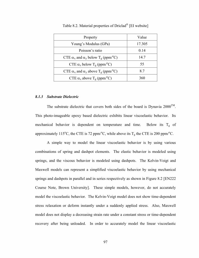
97
Table 8.2. Material properties of Driclad® [EI website]
8.1.3 Substrate Dielectric
The substrate dielectric that covers both sides of the board is Dynavia 2000TM.
This photo-imageable epoxy based dielectric exhibits linear viscoelastic behavior. Its
mechanical behavior is dependent on temperature and time. Below its Tg of
approximately 115oC, the CTE is 72 ppm/oC, while above its Tg the CTE is 200 ppm/oC.
A simple way to model the linear viscoelastic behavior is by using various
combinations of spring and dashpot elements. The elastic behavior is modeled using
springs, and the viscous behavior is modeled using dashpots. The Kelvin-Voigt and
Maxwell models can represent a simplified viscoelastic behavior by using mechanical
springs and dashpots in parallel and in series respectively as shown in Figure 8.2 [EN222
Course Note, Brown University]. These simple models, however, do not accurately
model the viscoelastic behavior. The Kelvin-Voigt model does not show time-dependent
stress relaxation or deform instantly under a suddenly applied stress. Also, Maxwell
model does not display a decreasing strain rate under a constant stress or time-dependent
recovery after being unloaded. In order to accurately model the linear viscoelastic
Property Value
Young’s Modulus (GPa) 17.305
Poisson’s ratio 0.14
CTE αx and αy below Tg (ppm/oC) 14.7
CTE αz below Tg (ppm/oC) 55
CTE αx and αy above Tg (ppm/oC) 8.7
CTE αz above Tg (ppm/oC) 360

98
behavior, a generalized Maxwell model was used. Essentially, it is a combination of
Kelvin-Voigt and Maxwell models. The Kelvin-Voigt models in parallel were used for
simulating creep, and the Maxwell models in series were used for simulating stress
relaxation [Findley et al., 1989]. This model is also known as Prony Series and is
represented in Equation 8.1.
( ) ( )i
N
iio GGG τξξ /exp
1−+= ∑
=
where, Go is the initial glassy modulus, N is the number of Maxwell elements, ξ is the
reduced time, and τ is the relaxation time. The Prony Series parameters are based from
Dynamic Mechanical Anaysis (DMA) measurement as listed in Table 8.3.
Figure 8.2. Various viscoelastic representations
G η
(a) Kelvin-Voigt model
G
η
(b) Maxwell model
(c) Generalized Maxwell model
G1
η G2

99
Table 8.3. Dynamic Mechanical Analysis measurement of Dynavia 2000TM [Ramakrishna, 2003]
8.1.4 Capacitor Dielectric
The dielectric material used in the capacitors was developed by EI Technologies,
Inc. The exact material chemical composition is proprietary, but it is a mixture of
polymer and ceramic based nano-particles to achieve relatively high dielectric constant
and stable material properties. This material was modeled as linear isotropic and
temperature dependent. Table 8.4 lists the mechanical and electrical material properties.
Relaxation time τi (sec) Extensional relaxation modulus weight factors (MPa)
7.19E-03 16.6368
9.05E-02 9.48133
1.14E+00 167.537
1.43E+01 136.641
1.81E+02 312.464
2.27E+03 330.227
2.86E+04 267.117
3.60E+05 251.494
4.54E+06 9.75963
5.71E+07 38.8723
7.19E+08 21.4291
E ( ∞ ) (rubbery) = 7.55

100
Table 8.4. Material properties of capacitor dielectric
8.2 Geometry Models and Assumptions
Physics-based numerical models were developed to qualitatively assess the failure
mechanisms of embedded capacitor. Both 2-D and 3-D finite element models were
developed to analyze the sequential buildup (SBU) process and the thermo-mechanical
electrostatic performance of embedded capacitors. Some of the assumptions made for the
finite element analysis and material models were:
• Due to the complex substrate structure, some of the minor geometric
features were ignored.
• The geometric dimensions were obtained from the cross-sectioning of the
structure. Any minor dimensional variations due to processing were
ignored.
• Although effort was made to accurately model the materials, limited access
to proprietary materials resulted in simplified material models.
• The electrostatic analysis assumes that the variation in the capacitance is
solely from thermo-mechanical deformation of capacitors. Material
Property Value
Young’s Modulus (GPa) 2.8
Poisson’s Ratio 0.34
CTE below 125oC (ppm/°C) 33.5
CTE above 125oC (ppm/°C) 60.7
Dielectric Constant at 1 MHz 22
Loss Factor at 1 MHz 0.016

101
degradations such as change in dielectric constant due to thermal excursions
were neglected.
All the material properties and important dimensional parameters are parametric,
and thus, they can be easily changed to analyze other materials or different geometric
dimensions. Four different cases were compared based on the copper probing pad
location and planar dimension to investigate their effects on the thermo-mechanical
reliability. As discussed in earlier chapter, probing pads are either located in the center or
the edge of the capacitor as shown in Figure 8.3. The main difference between them is
center probe has a hole in the center of top electrode while the edge probe has extended
bottom electrode. In terms of electrical performance, center probes are preferred due to
less parasitic inductance than edge probes; however, it is unknown which performs better
in terms of thermo-mechanical reliability. For this comparison, actual dimensions were
slightly modified to keep all the relative dimensions equal except the location of vias. In
addition, identical mesh density for both models was used.
Figure 8.3. Comparison between edge probe and center probe
Side View
Edge probes Center probes
Top View
Microvias
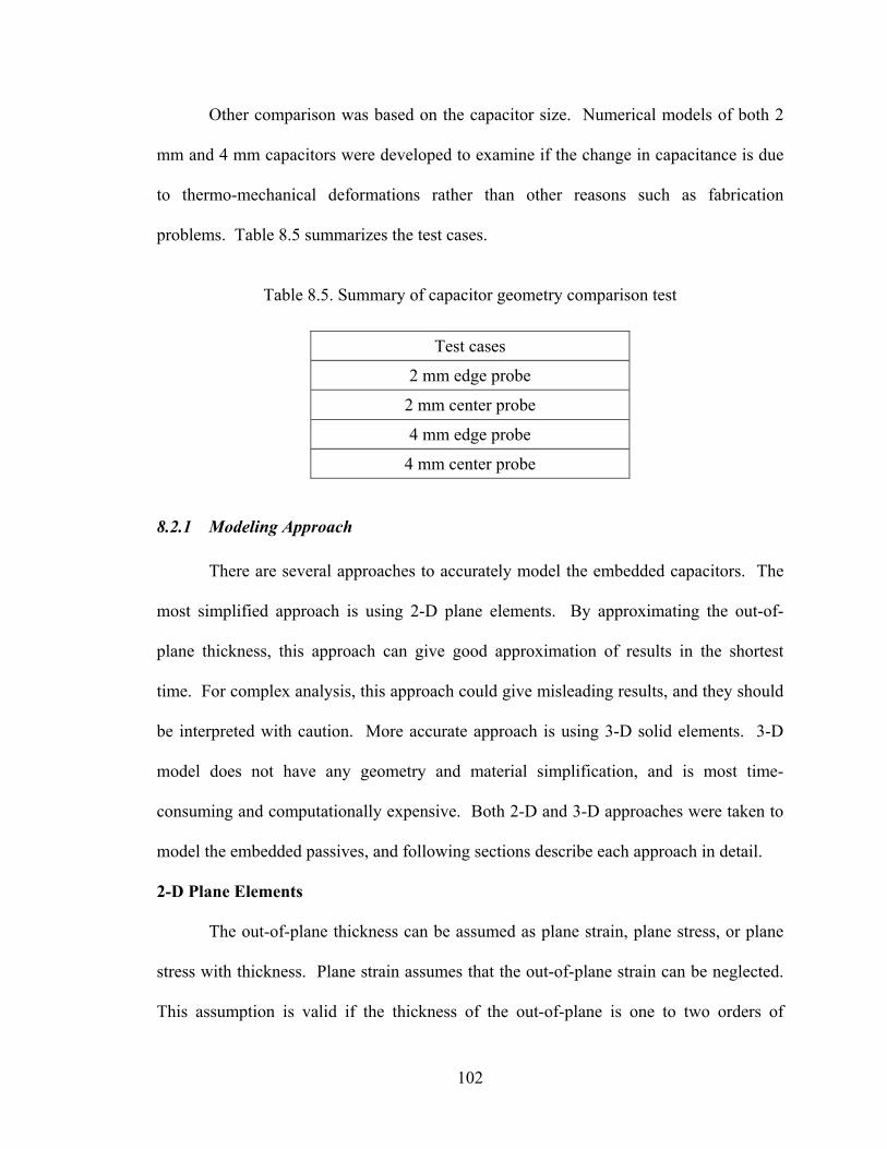
102
Other comparison was based on the capacitor size. Numerical models of both 2
mm and 4 mm capacitors were developed to examine if the change in capacitance is due
to thermo-mechanical deformations rather than other reasons such as fabrication
problems. Table 8.5 summarizes the test cases.
Table 8.5. Summary of capacitor geometry comparison test
8.2.1 Modeling Approach
There are several approaches to accurately model the embedded capacitors. The
most simplified approach is using 2-D plane elements. By approximating the out-of-
plane thickness, this approach can give good approximation of results in the shortest
time. For complex analysis, this approach could give misleading results, and they should
be interpreted with caution. More accurate approach is using 3-D solid elements. 3-D
model does not have any geometry and material simplification, and is most time-
consuming and computationally expensive. Both 2-D and 3-D approaches were taken to
model the embedded passives, and following sections describe each approach in detail.
2-D Plane Elements
The out-of-plane thickness can be assumed as plane strain, plane stress, or plane
stress with thickness. Plane strain assumes that the out-of-plane strain can be neglected.
This assumption is valid if the thickness of the out-of-plane is one to two orders of
Test cases
2 mm edge probe
2 mm center probe
4 mm edge probe
4 mm center probe

103
magnitude larger than the planar dimensions. Similarly, plane stress assumes that the
out-of-plane stress can be neglected. This assumption is valid if the thickness of the out-
of-plane is much smaller than the planar dimensions. Lastly, plane stress with thickness
defines a finite out-of-plane thickness.
For all 2-D analyses, PLANE183 (ANSYSTM) quadratic element with plane stress
with thickness assumption was used. Only half of the capacitor was actually modeled
with the assumption that the left side and right side is symmetric along the center line.
To apply this symmetry boundary condition, the nodes on the left edge were constrained
in the x-direction. In addition, the bottom left corner node was constrained in the y-
direction to prevent any rigid body motion. Figures 8.4 and 8.5 show the geometry of the
2-D edge probe and center probe capacitors respectively, and Table 8.6 lists the
dimensions.
Figure 8.4. 2-D edge probe capacitor with material identifications
Copper
Copper
Driclad®
Dynavia 2000TM
Dielectric
X
Y
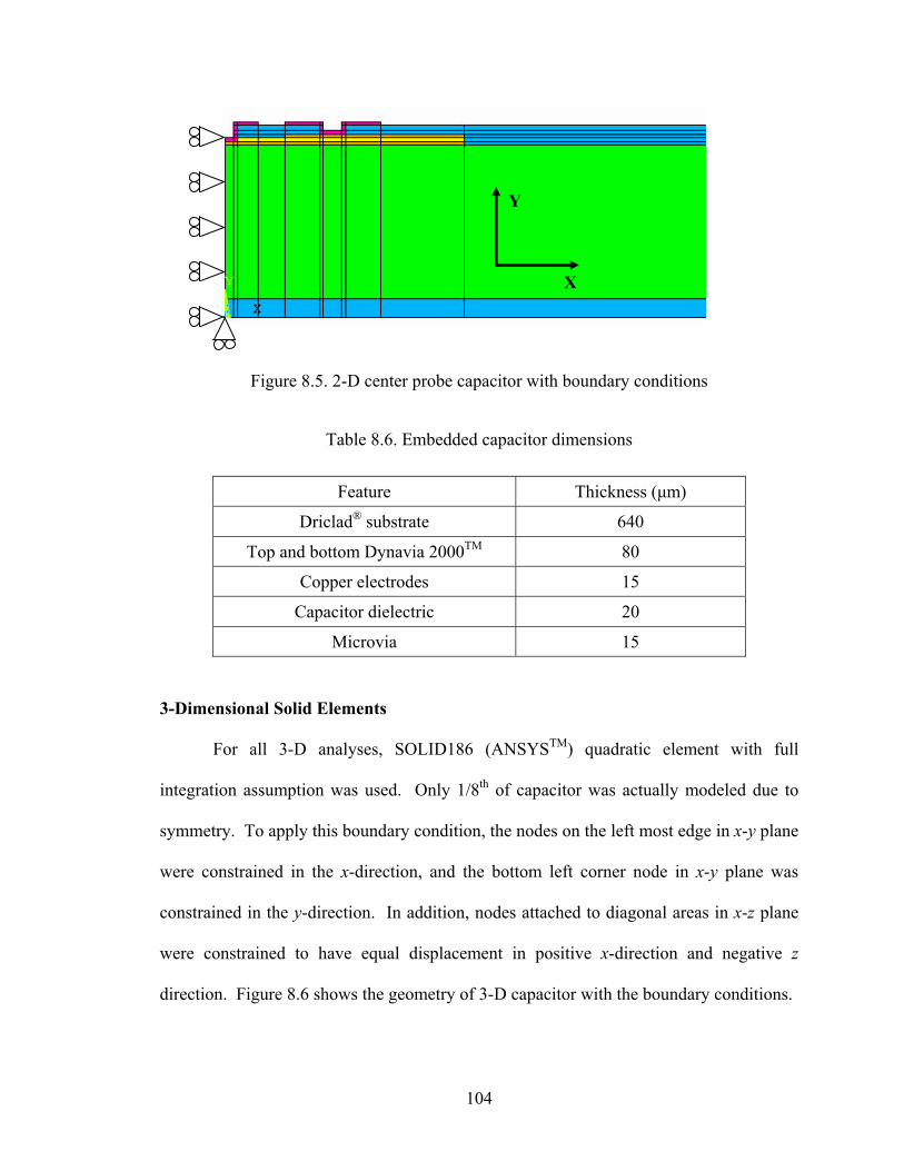
104
Figure 8.5. 2-D center probe capacitor with boundary conditions
Table 8.6. Embedded capacitor dimensions
3-Dimensional Solid Elements
For all 3-D analyses, SOLID186 (ANSYSTM) quadratic element with full
integration assumption was used. Only 1/8th of capacitor was actually modeled due to
symmetry. To apply this boundary condition, the nodes on the left most edge in x-y plane
were constrained in the x-direction, and the bottom left corner node in x-y plane was
constrained in the y-direction. In addition, nodes attached to diagonal areas in x-z plane
were constrained to have equal displacement in positive x-direction and negative z
direction. Figure 8.6 shows the geometry of 3-D capacitor with the boundary conditions.
Feature Thickness (µm)
Driclad® substrate 640
Top and bottom Dynavia 2000TM 80
Copper electrodes 15
Capacitor dielectric 20
Microvia 15
X
Y

105
Figure 8.6. 3-D center probe capacitor with boundary conditions
8.3 Process Modeling
During the SBU fabrication process, each layer is created at different process
conditions. Some require curing at high temperatures, while others are built at room
temperatures. The substrate experiences various thermal loads during the assembly, and
sometimes these processing conditions could build up significant residual stresses on the
substrate. Consequently, it is necessary to analyze the effect of process conditions.
Process modeling was completed by using element birth-and-death feature in
ANSYSTM. This analysis technique allows deactivation or reactivation of selected
elements to simulate the SBU process [ANSYS, 2004]. When deactivated, the stiffness
X
Y
Z
Copper
Copper
Driclad®
Dynavia 2000TM
Dielectric

106
of the “dead” elements is multiplied by a reduction factor (1.0 E-6) so that the “dead”
elements do not contribute any stiffness to the model. Also, any element loads or mass
associated with the dead elements are zeroed out and removed from other calculations.
When the elements are reactivated, their stiffness, mass, and element loads return to their
original values. This element birth-and-death feature is different from merely changing
the material property of certain elements, because the strain history of reactivated
elements is not maintained. Just changing the material property will retain the initial
strain experienced by the elements as they are born into the displaced node configuration.
The process model assumes the structure to be stress-free at the curing stage of
capacitor dielectric at 150oC. After curing, the substrate was brought down to room
temperature for the lamination of substrate dielectric. The dielectric was then cured at
135oC for 1 hour, and the entire board was brought down to room temperature.
Electroless copper plating of seed layers and electroplating of probing pads were
completed at room temperature. Figure 8.7 shows the thermal load profile.
Figure 8.7. Thermal load profile for process model
0
40
80
120
160
Load steps
Tem
pera
ture
(C)
Capacitor dielectric cure
Substrate dielectric cure
Microvia formation

107
8.3.1 Process Modeling Results
Finite element analysis of process modeling focused on several thermo-
mechanical concerns including: warpage, dielectric cracking, and interfacial
delamination. Axial stresses and von Mises stresses were used as damage metric for
dielectric crack growth, and peel stresses were used as damage metric for interfacial
delamination. Figures 8.8 to 8.10 show typical warpage and stress distributions based on
2 mm edge probe capacitor, and Figures 8.11 to 8.13 compares the results from four
cases. All the results were based on 2-D plane stress with thickness models.
Figure 8.8. Board warpage after assembly process
Figure 8.9. Axial stress distribution
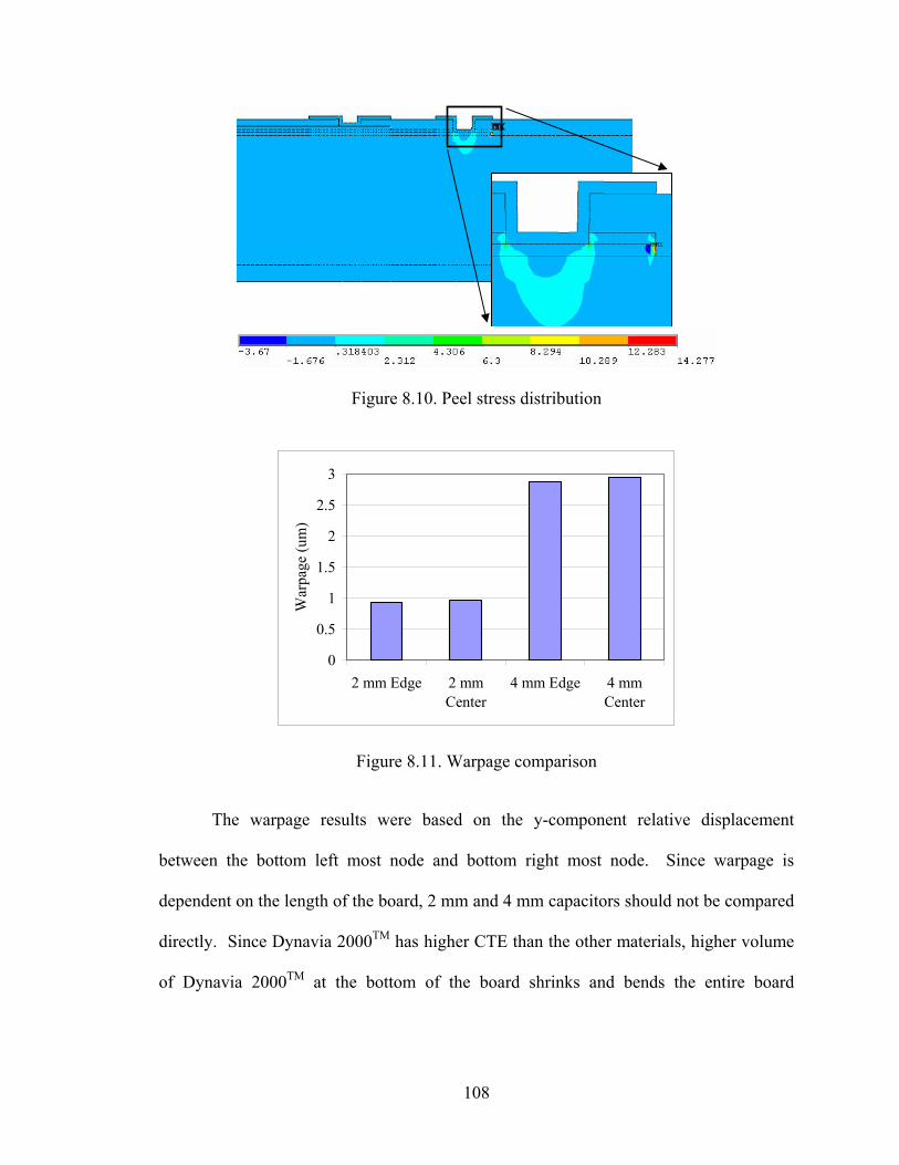
108
Figure 8.10. Peel stress distribution
0
0.5
1
1.5
2
2.5
3
2 mm Edge 2 mmCenter
4 mm Edge 4 mmCenter
War
page
(um
)
Figure 8.11. Warpage comparison
The warpage results were based on the y-component relative displacement
between the bottom left most node and bottom right most node. Since warpage is
dependent on the length of the board, 2 mm and 4 mm capacitors should not be compared
directly. Since Dynavia 2000TM has higher CTE than the other materials, higher volume
of Dynavia 2000TM at the bottom of the board shrinks and bends the entire board

109
downwards. For both 2 mm and 4 mm capacitors, probe location has very little effect on
the warpage of entire board.
-25
-20
-15
-10
-5
0
2 mm Edge 2 mmCenter
4 mm Edge 4 mmCenter
Stre
ss (M
Pa)
Axial stress von Mises stress
Figure 8.12. Axial and von Mises stresses
0
2
4
6
8
10
12
2 mm Edge 2 mmCenter
4 mm Edge 4 mmCenter
Inte
rfac
ial S
tress
(Mpa
)
Figure 8.13. Peel stress comparison
Stress results were based on the maximum stress observed. As shown in Figure
8.12, the capacitor planar dimensions or the probe location does not seem to affect the

110
axial stress or von Mises stress. All four cases showed similar axial stresses of -19 MPa
and von Mises stresses of -23.5 MPa. This is expected since the axial stresses are
dependent on thickness of the build-up layers and the material moduli. In terms of
interfacial delamination, the maximum interfacial peel stresses were observed near the
edge of the capacitor between the copper and capacitor dielectric layers. As shown in
Figure 8.13, the planar dimensions of capacitor does not seem to affect the results;
however, edge probes show almost three times higher interfacial peel stresses than the
center probes. Although this model is more qualitative and adhesion is dependent on
numerous factors, literature review suggests that these stress levels could cause
delamination. Kupfer [2000] reported interfacial strength between Cu and various
polymers to be between 10 to 25 MPa depending on the surface treatments.
8.4 Thermo-Mechanical Electrostatic Model
Thermo-mechanical electrostatic analyses were performed to understand the
thermo-mechanical behaviors and their effects on the performance of embedded
capacitors. It is essentially a two-step process. First, thermo-mechanical analysis was
performed to investigate the deformation of the capacitor, and then its displacement
boundary condition was transferred to electrostatic analysis to investigate its effect on the
capacitance. The temperature range of thermal cycling simulation was -40 to 125oC as
shown in Figure 8.14.

111
-60-30
0306090
120150
1 5 9
Load Steps
Tem
pera
ture
(o C)
Figure 8.14. Thermal cycling load profile
8.4.1 Electrostatic analysis
Electrostatic analysis was based on the electrical potential energy stored in the
dielectric material. The magnitude of the electrical potential energy and its relationship
between the capacitance are represented in Equations 8.1 and 8.2.
∫ •=V
DdvEU21 (Eq. 8.1)
( )2
21
2VV
UC−
= (Eq. 8.2)
U is the magnitude of electrical potential energy, E is electric field, D is electric distance,
V is electrical potential, C is the capacitance, and V1 and V2 are the applied voltage on top
and bottom electrodes respectably. When the voltage is applied on the electrodes,
positive and negative charges within the dielectric material shift towards the electrodes in
opposite direction. This creates the polarization within the dielectric and stores electrical

112
energy. Numerical model follows a similar approach. When different voltage values are
applied on the top and bottom electrodes, the dielectric material stores electrical energy
based on its dielectric constant. The magnitude of electrical potential energy at each
element associated with the dielectric material can be added to obtain the total energy
stored. Then, the capacitance can be calculated by Equation 8.2
8.4.2 Thermo-Mechanical Electrostatic Analysis Results
3-D models were used to complete all thermo-mechanical electrostatic analyses.
Thickness of all capacitors is assumed as 15 µm based on test case 1. Table 8.7 compares
the capacitance before the deformation with the theoretical calculation using Equation
8.3.
tA
C rε= (Eq. 8.3)
C is capacitance, εr is the relative permeability of dielectric, A is the area of effective
capacitor electrodes, and t is the thickness of dielectric.
Table 8.7. Comparison between the theoretical and simulated capacitance
Test cases Theoretical capacitance (pF)
Simulated capacitance before deformation (pF)
Comparison (%)
2 mm edge 51.94 52.32 - 0.73
2 mm center 48.70 49.25 - 1.13
4 mm edge 207.77 208.34 - 0.27
4 mm center 204.53 204.86 - 0.16

113
Although theoretical capacitances are very similar to the simulated results, all four cases
show slightly higher simulation results as listed in Table 8.7. This is expected due to the
extra area of capacitor electrodes that is not considered in the theoretical calculations.
The small tab of extension on the edge probe capacitors and the via areas of center probes
do store electrical charge and contribute to the capacitance calculation. Table 8.8 lists the
change in capacitance before and after the thermal cycling simulation.
Table 8.8. Comparison of change in capacitance
Overall, there is less than 1% change in capacitance after thermal cycling simulation.
These results are much smaller than the experimental results, where 110 mil (2.79 mm)
square capacitor showed approximately 3% change in capacitance after identical thermal
cycling. This is most likely due to inadequate material models. The simulation results
are only based on the thermo-mechanical deformation, and any material degradation is
not considered since they were not available. Inclusion of change in dielectric constant
due to thermal cycling should show closer results.
Test cases Simulated
capacitance before cycling (pF)
Simulated capacitance after
cycling (pF)
Comparison (%)
2 mm edge 52.32 52.44 0.23
2 mm center 49.25 49.36 0.22
4 mm edge 208.34 208.83 0.24
4 mm center 204.86 205.35 0.24

114
CHAPTER IX
CONCLUSION AND FUTURE WORK
9.1 Conclusion
This thesis made contributions to overall development of embedded passives by
focusing on the design and fabrication as well as the experimental and theoretical
reliability assessments. Experimental study was based on the fabrication of test vehicles
and various reliability qualification tests. Theoretical modeling study was based on the
development of numerical models that simulate the fabrication process conditions and
thermal cycling. The summary and contributions of this thesis are:
• Embedded capacitors and resistors with different geometric shapes, planar
dimensions, and thus different electrical characteristics were fabricated in a
multilayered organic substrate.
• Capacitors are made with polymer/ceramic nanocomposite materials and
have a capacitance in the range of 50 pF to 1.5 nF with specific capacitance
of approximate 1.4 nF/cm2.
• Resistors are carbon ink based PTF and NiCrAlSi and have a resistance in
the range of 25 Ω to 400 kΩ.
• High frequency measurements of capacitors showed stable capacitance from
200 MHz to 1.8 GHz and resonant frequency at 900 MHz.
• Various accelerated reliability qualification tests including thermal cycling
(-40 to 125oC and -55 to 125oC), constant temperature and humidity tests

115
(85oC/ 85%RH), and HAST (121oC/ 100%RH) based on JEDEC and MIL
standards were performed.
• Accelerated tests showed PTF resistors with less than 5% change in
resistance and NiCrAlSi resistors with less than 1% change in resistance.
• Accelerated tests showed some capacitor test vehicles with more than 20%
change in capacitance, while others only showed less than 5% change.
Such dramatic change is most likely due to fabrication problems.
• Various geometric shapes and planar dimensions of resistors and capacitors
were compared after accelerated tests. No clear dependence of geometric
shapes and planar dimensions were shown.
• TCR and TCC of TV1 were measured to characterize the materials.
• Numerical models of capacitor were developed to analyze the fabrication
process conditions and thermal cycling. All the material properties and
important dimensional parameters are parametric, and thus, they can be
easily changed to analyze other materials or different geometric dimensions.
• Two different probing pad locations and two sizes of capacitors were
numerically compared. Center probes showed higher warpage and
interfacial stresses than edge probes.
• Thermo-mechanical electrostatic analyses were performed and investigated
the change in capacitance due to thermo-mechanical deformation. Less
than 1% change in capacitance was shown due to thermo-mechanical
deformation.

116
9.2 Future Work
Over the last several years, tremendous progresses have been made in embedded
passive technology. Some of recommendations for future work are:
• Perform other experimental characterization such as break down voltage to
help understand the embedded passive behaviors.
• Develop numerical models to characterize high frequency performance of
capacitors
• Perform more accurate material characterizations to qualitatively study the
failure mechanisms.
• Analyze different dielectric material systems to compare their thermo-
mechanical reliability

117
APPENDIX A: Detailed Fabrication Steps
Appendix A.1. Detailed embedded capacitor fabrication processes and conditions
Surface preparation Acetone bath and microetch for 2 minutes to thoroughly clean the surface and improve adhesion.
Bond film to improve adhesion
Bond film is a 3 step process:
Cleaner at 40 – 55oC for 4 minutes
Rinse with DI water for 2 minutes
Activator at 25 – 45oC for 2 minutes
No Rinse
Bond solution at 35 – 45oC for 2 minutes
Rinse with DI water for 2 minutes
Board was baked at 90oC for 30 minutes to remove moisture.
Nanocomposite preparation
Mix 44 g of barium titanate based polymeric resin with 4.24 g of hardener and 5 g of thinner for 1 hour.
Spin coat nanocomposite
Spin coat at 2000 rpm for 30 seconds with 500 rpm ramp rate.
Board was baked at 65oC for 45 minutes to remove moisture.
Copper lamination Drawer Vacuum Laminator
Heat press to strengthen copper
lamination 2 tons press applied at 70oC for 20 minutes.
Surface preparation Acetone bath and microetch for 2 minutes to thoroughly clean the surface and improve adhesion.
Board was baked at 70oC for 30 minutes to remove moisture
Spin coat photoresist Shipley SP20-29 positive liquid photoresist was spin coated at 1000 rpm for 30 seconds.
Board was baked at 70oC for 30 minutes to remove moisture.
UV exposure to pattern top electrode
UV exposure of 200 – 300 mJ/cm2 performed on Tamarack 152R contact printer under vacuum hard contact with a Mylar photo tool.

118
Develop exposed photoresist
12% Photoposit 303A developer at 26 – 32oC for 1 – 3 minutes with mild agitation
Board was baked at 70oC for 30 minutes to remove moisture.
Etch copper Exposed copper area removed with 30% Ferric Chloride for 15 minutes
Strip nanocomposite and photoresist
Nanocomposite and remaining photoresist were flat UV exposed for 2 minutes.
Gamma Butyrolactone (GBL) solvent was sprayed for 10 minutes to strip the nanocomposite and photoresist.
Board was fully cured at 150oC for 1 hour to complete the process.

119
Appendix A.2. Detailed embedded resistor fabrication processes and conditions
Surface preparation Acetone bath and microetch for 2 minutes to thoroughly clean the surface and improve adhesion.
Laminate dry photoresist
Dupont Riston 4615 dry film (30 µm thick) was vacuum laminated on the board.
UV exposure UV exposure of ~300 mJ/cm2 performed on Tamarack 152R contact printer under vacuum hard contact with a Mylar photo tool.
Develop photoresist to get pattern
1% Sodium Carbonate at 45oC was used for 2 minutes to develop the photoresist.
Board was baked at 70oC for 30 minutes to remove moisture.
Apply Carbon Ink resist material
The Carbon Ink was squeezed into the developed negative pattern of the resist trace.
Board was baked at 120oC for 1 hour to harden the resist material.
Strip photoresist
3% Sodium Hydroxide at 55oC was used to strip the photoresist.
Finally, the board was cured at 150oC for 1 hour to complete the process.

120
Appendix A.3. Detailed microvia fabrication processes and conditions
Surface preparation Acetone bath and microetch for 2 minutes to thoroughly clean the surface and improve adhesion.
Spin coat photoresist
Photoepoxy dielectric (Vantico Probimer 7081) was spin coated at 1000 rpm for 40 seconds to achieve a nominal thickness of 30 µm.
Board was baked at 90oC for 30 minutes to remove moisture.
UV exposure
UV exposure of ~4,000 mJ/cm2 performed on Tamarack 152R contact printer under vacuum hard contact with a Mylar photo tool.
Board was baked at 110oC for 1 hour to fully crosslink the exposed area.
Develop photoresist to open up microvias
Gamma Butyrolactone (GBL) solvent at room temperature was used for ~3 minutes to develop the photoresist.
Remaining photoresist was flat exposed with ~4,000 mJ/cm2.
Board was fully cured at 160oC for 1 hour.
Electroless copper plating to build a seed
layer
Electroless copper plating is a 8 step process:
Swell at 70oC for 8 minutes
Rinse with DI water for 2 minutes
Etch at 77oC for 7 minutes
Rinse with DI water for 2 minutes
Neutralizer at 40oC for 2 minutes
Rinse with DI water for 2 minutes
Conditioner at 65oC for 6 minutes
Rinse with DI water for 2 minutes
Predip at room temperature for 1 minute
Rinse with DI water for 2 minutes
Activator at 40oC for 6 minutes
Dip in DI water for 20 seconds
Reducer at 27oC for 5 minutes
Dip in DI water for 20 seconds

121
Electroless copper bath at 34oC for < 2 minutes
Board was baked at 120oC for 1 hour.
Laminate dry photoresist to build
microvias and copper pads
Dupont Riston FX515 dry film (15 µm thick) was vacuum laminated on the board.
UV exposure
UV exposure of 105 mJ/cm2 performed on Tamarack 152R contact printer under vacuum hard contact with a Mylar photo tool.
Board was baked at 90oC for 10 minutes to harden the photoresist.
Develop photoresist to get pattern
1% Sodium Carbonate at 45oC was used for 2 minutes to develop the photoresist.
Electroplating copper to build microvias
Direct current of 1.25 A was applied for 8 minutes for each of 4 rotations to achieve the target thickness of 8 -10 µm.
Strip photoresist 3% Sodium Hydroxide at 55oC was used to strip the photoresist.
Microetch copper The seed electroless copper layer was microetched to complete the process.

122
REFERENCES
1. http://www.3m.com/us/electronics_mfg/microelectronic_packaging, 3M website, Accessed 2005.
2. http://www.cascademicrotech.com, Cascade Microtech website, Accessed 2005.
3. http://www.dupont.com/fcm/interra/products/ceramic.html, DuPont website, Accessed 2005.
4. http://electronicmaterials.rohmhaas.com/, Rohm and Hass Website, Accessed 2005.
5. http://www.engin.brown.edu/courses/En222/Notes/Viscoelast/Viscoelast.htm, EN222: Mechanics of Solids Course Notes, Brown University, Accessed 2005.
6. http://www.gould.com/sp_tcr.htm, Gould website, Accessed 2004.
7. http://www.macdermid.com, MacDermid website, Accessed 2005.
8. http://www.ohmega.com/OhmPly.html, Ohmega website, Accessed 2005.
9. http://www.prc.gatech.edu, Packaging Research Center website, Accessed 2004.
10. http://www.sanmina-sci.com/Solutions/pdfs/Buried_Capacitance.pdf, Sanmina website, Accessed 2005.
11. ANSYS, Inc. Theory Manual, Release 8.1, 2004.
12. Berry, R., Hall, P., and Harris, M., Thin Film Technology, Van Nostrand, New York, 1968
13. Berry, R., Sloan, D., “Tantalum Printed Capacitors,” Proceedings of the IRE, 1959.
14. Borland, W., Felton, J.J., Dellis, L.E., Ferguson, S., Majumdar, D. Jones, A. B., Lux, M.S., Traylor, R.R., Doyle, M., “Ceramic Resistors and Capacitors Embedded In Organic Printed Wiring Boards” Proceedings of International Electronic Packaging Technical Conference and Exhibition, July 2003, pp. 797-800.
15. Chahal, P. et al., “Electroless Ni-P/Ni-W-P Thin-Film Resistors for MCM-L Based Technologies,” Proceedings of the 48th Electronic Component and Technology Conference, 1998, pp. 232, 1998.

123
16. Chen, K., Brown, W.D., Schaper, L.W., Ang, S.S., Naseem, H.A., “A Study of the High Frequency Performance of Thin Film Capacitors for Electronic Packaging,” IEEE Transactions on Advanced Packaging, v 23, n 2, May 2000, pp. 293-302.
17. Coates, K., Chien, C.P., Hsiao, Y.Y.R., Kovach, D.J., Tang, C.H., Tanielian, M.H., “Development of Thin Film Resistors for Use in Multichip Modules,” 1998 International Conference on Multichip Modules and High Density Packaging, IEEE, 1998, pp. 490-495.
18. Damani, M., “Physics-Based Reliability Assessment of Embedded Passives,” Masters Thesis, Georgia Institute of Technology, Atlanta, GA, 2004
19. Damani, M., Pucha, R.V., Bhattacharya, S., Tummala, R., and Sitaraman, S.K., "Physics-based Reliability Assessment of Embedded Passives," 54th Electronic Components and Technology Conference, IEEE-CPMT and EIA, Las Vegas, NV, June 2004, pp. 2027-2031.
20. D’Ambrisi, J., Fritz, D., and Sawoska, D., “Plated Embedded Resistors for High Speed Circuit Applications,” IPC Fall Annual Meeting, Orlando, FL, 2001.
21. Diaz-Alvarez, E., and Krusius, J., “Modeling and Simulation of Integrated Capacitors for High Frequency Chip Power Decoupling,” IEEE Transactions on Components and Packaging Technologies, v 23, n 4, Dec. 2000, pp. 611-619.
22. Dunne, R.C., ”An Integrated Process Modeling Methodology and Module for Sequential Multi-layered high-density substrate fabrication for microelectronic packages” Ph.D. Thesis, Georgia Institute of Technology, Atlanta, GA, 2000.
23. Dunne, R.C., Sitaraman, S.K., Shijian L., Wong, C.P., Estes, W.E., Periyasamy, M., “Cure kinetics modeling of ViaLuxTM 81: a novel epoxy photodielectric dry film (PDDF) for microvia applications,” International Symposium on Advanced Packaging Materials: Processes, Properties and Interfaces, 2000, pp. 254 -260.
24. Fairchild, K., Morcan, G., Lenihan, T.,; Brown, W., Schaper, L., Ang, S., Sommers, W., Parkerson, J., Glover, M., “Reliability of Flexible Thin-Film Embedded Resistors and Electrical Characterization of Thin-Film Embedded Capacitors and Inductors,” Proceedings of the 47th Electronic Component and Technology Conference, 1997, pp. 730-738.
25. Findley, W. N., Lai, J. S. and K. Onaran, Creep and Relaxation of Nonlinear Viscoelastic Materials: With an Introduction to Linear Viscoelasticity, Dover Publications, Inc., New York, 1989.
26. Garrou, P., “Polymer Dielectrics for Multichip Module Packaging,” Proceedings of the IEEE, v 80, n 12, Dec. 1992, pp. 1942-1954

124
27. Halliday, D., Resnick, R., Walker, J., Fundamentals of Physics, John Wiley & Sons, New York, 1997.
28. Hassell, P., “Advanced Warpage Characterization: Location and Type of Displacement Can be Equally as Important as Magnitude,” Proceedings of Pan Pacific Microelectronics Symposium Conference, Feb. 2001, pp 163-169.
29. Hendrix, B., and Stauf, G., “Low Temperature Process for High Density Thin Film Integrated Capacitors,” Proceedings of the 2000 Conference on High-Density Interconnect and Systems Packaging, 2000, pp. 342-345.
30. Iannuzzelli, R., “Predicting Plated-Through-Hole Reliability in High Temperature Manufacturing Process” Proceedings of the 41st Electronics and Technology Conference, 1991, pp 410-442.
31. Hegde, S., “Low-Stress Dielectric for Multilayered Structures,” Masters Thesis, Georgia Institute of Technology, Atlanta, GA, 2004.
32. Kupfer, H. and Wolf, G.K., “Plasma and Ion Beam Assisted Metallization of Polymers and their applications,” Nuclear Instruments and Methods in Physics Research B 166-167, 2000, pp. 722-731.
33. Ladew, R. and Makl, A., “Integrating Passive Components,” In ISHM ’95 Proceddings, 1995, pp. 59.
34. Lee, K.J., Bhattacharya, S., Varadarajan, M., Wan, L., Abothu, I.R., Sundaram, V., Muthana, P., Balaraman, D., Raj, P.M., Swaminathan, M., Sitaraman, S.K. and Tummala, R.R., "Deign, Fabrication and Reliability assessment of embedded resistors and capacitors on multilayered microvia organic substrates", Proceedings of the IEEE-CPMT International Symposium and Exhibition on Advanced Packaging Materials, Irvine, CA, March 16-18, 2005, pp. 249-254.
35. Lee, K.J., Pucha, R., Varadarajan, M., Bhattacharya, S., Tummala, R., and Sitaraman, S.K., “Reliability Assessment of Embedded Capacitors in Multilayered Microvia Organic Substrate,” IMAPS 2005, Philadelphia, PA, Sept. 2005.
36. Maissel, L., and Glang, R., Handbook of Thin Film Technology, McGraw-Hill, New York, 1970.
37. National Electronic Manufacturing Initiative Roadmap, 2004 edition, “Passive Components,” 2004, pp. 5.
38. Nelms, D., Ulrich, R., Schaper, L., Reeder, S., “Anodization for Forming Thin Film Embedded Capacitors in MCM-D and MCM-L substrates,” Proceedings of the 48th Electronic Component Technology Conference, 1998, pp. 247.

125
39. Nielsen, M., Cole, H., Saia, R.J., Durocher, K.M., Krishnamurthy, N., Kapadia, H., Lu, T.M., Rymaszewski, E.J., Dey, S., Shaefer, T., Gilbert, B., “Demonstration of Integral Passives on Double Sided Polyimide Flex,” Proceedings of the 2000 Conference on High-Density Interconnect and Systems Packaging, 2000, pp. 351-356.
40. Novak, I., Miller, J. R., “Frequency Dependent Characterization of Bulk and Ceramic Bypass Capacitors”, Poster material for the 12th Topical Meeting on Electrical Performance of Electronic Packaging, Oct. 2003.
41. Rao, Y., “High Dielectric Constant Material Development and Electrical Simulation of Embedded Capacitors,” Ph.D. Thesis, Georgia Institute of Technology, Atlanta, GA, 2001
42. Rao, Y., Qu, J., Wong, C. P., “RF Electrical Simulation of Embedded Capacitor”, Proceedings of the IEEE-CPMT International Symposium and Exhibition on Advanced Packaging Materials, Braselton, GA, March 11-14, 2001, pp. 286-292.
43. Ramakrishna, G., Liu, F., and Sitaraman, S. K., "Experimental and Numerical Investigation of Microvia Reliability", ITHERM'2002, The 8th Intersociety Conference on Thermal and Thermo-mechanical Phenomena in Electronic Systems, IEEE-CPMT, ASME, and IMAPS, San Diego, CA, May 1, 2002, pp. 932-939.
44. Schatzel, D. “Development of Reliable Electronic Packaging Solutions for Spacecraft Avionics Miniaturization Using Embedded Passives Devices” Proceedings of International Electronic Packaging Technical Conference and Exhibition, July 2003, pp. 797-800.
45. Sergent, J., and Harper, C., Hybrid Microelectronics Handbook, 2nd ed., McGraw-Hill, New York, 1995.
46. Shibuya, A., Matsui, K., Takahashi, K., Kawatani, A., “Embedded TiNxOy Thin-Film Resistors in a Build-Up CSP for 10 Gbps Optical Transmitter and Receiver Modules,” Proceedings of the 51st Electronic Components and Technology Conference, 2001, pp. 847-851.
47. Strydom, J.T., Wyk, J.D.V., “Investigation of Thermally Induced Failure Mechanisms in Integrated Spiral Planar Power Passives” 37th IAS Annual Meeting. Conference Record of the Industry Applications Conference, v 3, Oct. 2002, pp. 1781–1786.
48. Tummala, R. R.; Rymaszewski, E. J.; Klopfenstein, A. G., Microelectronics Packaging Handbook, 2nd Edition, Chapman and Hall, New York, 1997.
49. Tummala, R. R., Fundamentals of Microsystems Packaging, McGraw-Hill, New York, 2001.

126
50. Ulrich, R., “Embedded Resistors and Capacitors for Organic-Based SOP”, IEEE Trans. Advanced Packaging, v 27, n 2, May 2004.
51. Ulrich, R.K. and Schaper, L.W., Integrated Passive Component Technology, IEEE Components, Packaging & Manufacturing Technology Society, 2004.
52. Xie, W., Sitaraman, S.K., “Numerical study of interfacial delamination in a system-on-package (SOP) integrated substrate under thermal loading,” The 7th Intersociety Conference on Thermal and Thermo-mechanical Phenomena in Electronic Systems, ITHERM 2000, v 2, 2000, pp. 356 -361.
53. Zhou, J., Myers, J.D., Felten, J.J. “Embedded Passives Technology for PCBs: Materials, Design and Process” International Microelectronics and Packaging Society, 2002