Microwave dielectric properties of La3Ti2TaO11 ceramics with perovskite-like layered structure
Upload
independentCategory
view
3download
0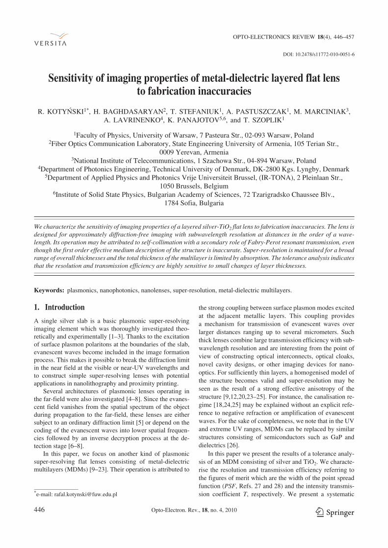
Sensitivity of imaging properties of metal-dielectric layered flat lensto fabrication inaccuracies
R. KOTYŃSKI1*, H. BAGHDASARYAN2, T. STEFANIUK1, A. PASTUSZCZAK1, M. MARCINIAK3,A. LAVRINENKO4, K. PANAJOTOV5,6, and T. SZOPLIK1
1Faculty of Physics, University of Warsaw, 7 Pasteura Str., 02−093 Warsaw, Poland2Fiber Optics Communication Laboratory, State Engineering University of Armenia, 105 Terian Str.,
0009 Yerevan, Armenia3National Institute of Telecommunications, 1 Szachowa Str., 04−894 Warsaw, Poland
4Department of Photonics Engineering, Technical University of Denmark, DK−2800 Kgs. Lyngby, Denmark5Department of Applied Physics and Photonics Vrije Universiteit Brussel, (IR−TONA), 2 Pleinlaan Str.,
1050 Brussels, Belgium6Institute of Solid State Physics, Bulgarian Academy of Sciences, 72 Tzarigradsko Chaussee Blv.,
1784 Sofia, Bulgaria
We characterize the sensitivity of imaging properties of a layered silver−TiO2 flat lens to fabrication inaccuracies. The lens isdesigned for approximately diffraction−free imaging with subwavelength resolution at distances in the order of a wave−length. Its operation may be attributed to self−collimation with a secondary role of Fabry−Perot resonant transmission, eventhough the first order effective medium description of the structure is inaccurate. Super−resolution is maintained for a broadrange of overall thicknesses and the total thickness of the multilayer is limited by absorption. The tolerance analysis indicatesthat the resolution and transmission efficiency are highly sensitive to small changes of layer thicknesses.
Keywords: plasmonics, nanophotonics, nanolenses, super−resolution, metal−dielectric multilayers.
1. Introduction
A single silver slab is a basic plasmonic super−resolvingimaging element which was thoroughly investigated theo−retically and experimentally [1–3]. Thanks to the excitationof surface plasmon polaritons at the boundaries of the slab,evanescent waves become included in the image formationprocess. This makes it possible to break the diffraction limitin the near field at the visible or near−UV wavelengths andto construct simple super−resolving lenses with potentialapplications in nanolithography and proximity printing.
Several architectures of plasmonic lenses operating inthe far−field were also investigated [4–8]. Since the evanes−cent field vanishes from the spatial spectrum of the objectduring propagation to the far−field, these lenses are eithersubject to an ordinary diffraction limit [5] or depend on thecoding of the evanescent waves into lower spatial frequen−cies followed by an inverse decryption process at the de−tection stage [6–8].
In this paper, we focus on another kind of plasmonicsuper−resolving flat lenses consisting of metal−dielectricmultilayers (MDMs) [9–23]. Their operation is attributed to
the strong coupling between surface plasmon modes excitedat the adjacent metallic layers. This coupling providesa mechanism for transmission of evanescent waves overlarger distances ranging up to several micrometers. Suchthick lenses combine large transmission efficiency with sub−wavelength resolution and are interesting from the point ofview of constructing optical interconnects, optical cloaks,novel cavity designs, or other imaging devices for nano−optics. For sufficiently thin layers, a homogenised model ofthe structure becomes valid and super−resolution may beseen as the result of a strong effective anisotropy of thestructure [9,12,20,23–25]. For instance, the canalisation re−gime [18,24,25] may be explained without an explicit refe−rence to negative refraction or amplification of evanescentwaves. For the sake of completeness, we note that in the UVand extreme UV ranges, MDMs can be replaced by similarstructures consisting of semiconductors such as GaP anddielectrics [26].
In this paper we present the results of a tolerance analy−sis of an MDM consisting of silver and TiO2. We characte−rise the resolution and transmission efficiency referring tothe figures of merit which are the width of the point spreadfunction (PSF, Refs. 27 and 28) and the intensity transmis−sion coefficient T, respectively. We present a systematic
446 Opto−Electron. Rev., 18, no. 4, 2010
OPTO−ELECTRONICS REVIEW 18(4), 446–457
DOI: 10.2478/s11772−010−0051−6
*e−mail: [email protected]
ana− lysis of the sensitivities of resolution and transmissionon the major parameters which define the structure fora broad range of the thicknesses of the MDM. We assess thesignificance of the parameters which define the structure tothe expected properties of the fabricated MDM.
2. Numerical characterisation of super-resolvingproperties of MDM
2.1. Numerical modelling of MDMA variety of frequency−domain and time−domain numeri−cal methods may be used to model light transmissionthrough metal−dielectric multilayers. Most of the numeri−cal results presented in this paper are obtained using thetransfer matrix method (TMM). They are compared withthe ones obtained by the method of single expression(MSE), the finite difference time domain method (FDTD),and the simplified approach based on the effectivemedium theory (EMT).
The multilayer structures consist of dispersive and ab−sorptive isotropic materials. We consider a CW coherentillumination, a planar two−dimensional geometry as shownin Fig. 1, and optically linear materials so that it is straight−forward to use frequency−domain modelling. The actualchallenge is in the accurate modelling of the super−resolvingproperties of the multilayer. The subwavelength size of theobject, which is imaged by the near−field propagationthrough the structure, has to be included in the simulationsthrough a careful choice of the incidence conditions. In anoptical experiment, the source could be realised with a sub−wavelength slit in a mask, a tip of a SNOM probe, a taperedfibre coupled to the lens input plane or a subwavelength sizeplasmonic waveguide. Such an element could be in princi−ple included in the FDTD simulations but not in the TMMor the MSE ones. Instead, the TMM and the MSE provideinformation on the transmission of individual propagatingor evanescent planewaves. This information is gathered todetermine the transfer function (TF) of the multilayer andthe corresponding point spread function (PSF) obtained asinverse Fourier transform of the TF.
In terms of Fourier optics, the imaging properties of any
linear and shift invariant system (LSI, also termed as iso-
planatic system), can be derived from the coherent ampli-
tude point spread function PSF x( ) or equivalently from the
transfer function TF x( ) of the system [27–29]. In our case,
the transfer function is defined as a complex amplitude
transmission coefficient �( )t kx
at the fixed parallel compo-
nent kx
of the wavevector of an incident propagating or eva-
nescent plane wave, i.e., TF t kx
� �( ). Note that we use
a caret to indicate the one-dimensional Fourier transform
and to distinguish the functions of kx
representing spatial
spectra from those of x representing spatial field distribu-
tions. For the TM polarisation, it is convenient to refer to the
perpendicular component Hy
of the magnetic field as the
simulation takes place in the x z� plane with imaging along
the z axis perpendicular to the layer boundaries (see Fig. 1).
In effect, we define the amplitude transfer function � ( )t kH x
of the system as the ratio between the spatial spectra of the
outgoing to the incident magnetic fields
� ( ) � ( ) � ( )t k H k H kH x y
outgoing
x y
incident
x� , (1)
where � ( )H ky
outgoing
xis the field at the output plane and
� ( )H ky
incident
xis the incident part of the field at the input
plane. Therefore, the ideal condition for perfect imaging is
� ( )t kH x
� 1. We note that kx
is conserved throughout all the
layers for any incident planewave.
The PSF and TF are interrelated by a Fourier transform
and, at the same time, the PSF is a complex amplitude distri-
bution at the output plane � ( )H xy
outgoingresulting from
a delta-like excitation at the front plane � ( ) ( )H x xy
incident � � .
The ideal condition for perfect imaging expressed in terms
of the PSF is PSF x xH
( ) ( )� � . It is more straightforward to
calculate the PSF with the FDTD method, while the TF with
the TMM or the MSE. Below, we shortly summarise the
details of the numerical modelling methods used by us in the
present paper:
� finite−difference time−domain method (FDTD), we usetwo implementations of the FDTD algorithm [30] – theopen source software Meep [31], and a commercial im−plementation Crystal Wave tool by Photon Design Ltd.,Oxford [32]. In both cases, we use a two−dimensionalsquare Yee grid terminated with a PML, the Drude dis−persion model for the silver layers, and a current sourcerepresenting a dipole (Crystal Wave) or Gaussian−
Opto−Electron. Rev., 18, no. 4, 2010 R. Kotyński 447
Fig. 1. Schematic of a periodic Ag−TiO2 multilayer: (a) symmetricgeometry and (b) asymmetric geometry.
−shaped beam (Meep). The Gaussian beam is further dif−fracted on a 3−nm aperture in a perfect electric conductor(PEC) attached to the multilayer to form an extremelynarrow beam, useful in the demonstration of superre−solution (Meep). The discretisation step is equal to 1 nm,and is fine enough to correctly address the sizes of thelayers in the stack. The time step is taken slightly belowthe Courant limit serving for 2D calculations. The MDMis separated from the PML, as well as from the sourcewith air−gaps, which are necessary to assure the stabilityof simulation. The results of the FDTD simulations areanalysed after reaching a steady state, when all transienteffects have died out. The complex representation of thefield is obtained by means of a simple spectral analysis.To estimate the PSF, a point dipole source is placed inclose proximity (of about 35 nm) to the first interface. Thetransmission is calculated as the transmitted to the incidentflux ratio, where the fluxes are evaluated at the 0.4−μmdetector plates placed 10 nm away from the MDM,
� method of single expression (MSE), MSE is a frequencydomain method. It has been originally introduced in Ref.33 for one−dimensional systems. More recently, it hasbeen generalised for layered structures illuminated atoblique incidence [34]. We note that the MSE may beused with dispersive and lossy materials, with negativeor complex values of permittivity. The relevant metal−−dielectric multilayer structure with negative permitti−vity of metallic layers has been already analysed by theMSE [35]. In the MSE, the boundary problem solutionstarts from the non−illuminated side of the structure( )z L� by reducing it to a Cauchy problem, i.e., to aninitial value problem. Setting up the initial values, an in−tegration of the set of differential equations completelyequivalent to the Helmholtz equation is carried out byusing the Runge−Kutta numerical integration method inMerson’s modification (the step size is changed auto−matically according to the given accuracy) towards theilluminated side ( )z � 0 where the amplitude of incidentfield and power reflection coefficient are restored [33].We have verified that for the MDM structures consid−ered in this paper, the transmission and reflection coeffi−cients calculated using MSE and TMM match up to theaccuracy of the numerical floating point representation.Therefore, these two methods may be considered asequivalent. We note that the TMM is much faster thanthe MSE since it does not involve the Runge−Kutta nu−merical integration. In the MSE, the form of the wave−function inside particular layers is not introduced explic−itly. Therefore, the MSE may be seen as a more generalmethod and for instance, it could be directly used forstructures containing optically nonlinear materials [36],
� transfer matrix method (TMM), TMM is a popular andan efficient quasi−analytical modelling method wellsuited for analysis of one−dimensional layered struc−tures [37]. The calculations are repeated independentlyfor planewaves with different angles of incidence. Theseresults are further combined to construct the transfer
function, and the PSF is calculated from the transferfunction with a Fourier Transform. We use an imple−mentation of the TMM developed at the University ofWarsaw. The algorithm involves some simplificationsresulting from the periodicity of the analysed structure.The results presented in this paper do not depend on thechoice between the direct transfer matrix multiplicationscheme and the more stable scheme known as the sca−ttering matrix method,
� effective medium theory (EMT), effective medium the-
ory allows us to approximate a periodic multilayer with
an equivalent homogeneous and anisotropic medium
[9,25]. The application of EMT is, however, limited to
structures with a small size of the elementary cell com-
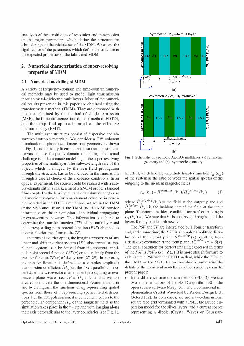
pared to the wavelength. In Fig. 2, we present a scheme
of a homogenised structure from Fig. 1. Optical proper-
ties of the effective medium are described with the uni-
axially anisotropic effective permittivity tensor �� shown
in Fig. 2. We calculate the transfer function and PSF of
metal-dielectric multilayers in the approximation of ef-
fective medium using the transfer matrix method ex-
tended to anisotropic materials.
2.2. Definition of the super-resolving Ag-TiO2 MDM
The multilayer consisting of Ag and TiO2 has been prelimi−narily optimised for subwavelength resolution at the wave−length of � = 441 nm. The single period of the multilayerconsists of a silver layer with the thickness dAg = (20�2)nmand TiO2 layer with the thickness dTiO2
= (22�2)nm. At thewavelength � = 441 nm, the respective refractive index ofTiO2 is n TiO2
2 47 0 02� �. . [38], while the refractive indexand extinction index of silver are n Ag � �0 04 0 02. . and� Ag � �2562 0 007. . [39]. We analyse the three variants ofthe multilayer presented in Figs. 1 and 2. The symmetricvariant shown in Fig. 1(a) has a symmetric elementary celland contains thinner, symmetric dielectric layers at its exter−
Sensitivity of imaging properties of metal−dielectric layered flat lens to fabrication inaccuracies
448 Opto−Electron. Rev., 18, no. 4, 2010 © 2010 SEP, Warsaw
Fig. 2. Uniaxially anisotropic slab consisting of an effective me−dium equivalent to the homogenised symmetric or asymmetric
Ag−TiO2 multilayers from Figs. 1(a) and 1(b).
nal boundaries. The asymmetric variant shown in Fig. 1(b)contains a leftmost external layer made of TiO2, and an ex−ternal rightmost layer made of silver. Finally, Fig. 2 presentsan equivalent slab made of a uniaxially anisotropic effectivemedium. The effective medium depends only on the fillingfraction of silver in the structure, therefore the same effec−tive medium results from the homogenisation of the sym−metric and asymmetric multilayers. We analyse structureswith the variable number of layers N. The information on theerrors of � � � � �n n d dAg Ag TiO Ag TiO, , , ,�
2 2will be used
in Sect. 3.An optimal layered lens can only be defined in the sense
of a trade−off between several criteria. A solution to multi−−criteria optimisation problem in a trade−off sense is definedas such that it is not possible to improve any of the consi−dered criteria without deteriorating the values of the otherones. We note that the optimality in a trade−off sense repre−sents a class of solutions rather than a unique result.
The FWHM of the PSF or PSF 2 [22,18] is a simplechoice for a measure of resolution. At the same time, thelens would be useless if the transmission efficiency T is notsufficient. Moreover, both FWHM and T usually deterioratewith the increase in the thickness of the lens. The lens thatwe consider is optimal in the sense of a trade−off betweenFWHM and T for the fixed number of layers N , whenN � 20 as well as for several other values of N , when
N � 20. This condition for optimality is satisfied for boththe symmetric as well as the asymmetric variant of the ge−ometry. Any change in the thickness of dAg or dTiO2
in ex−cess of 1 nm deteriorates at least one of the criteria ofFWHM and T. Therefore the lens is optimal in the trade−offsense between the two criteria. Nonetheless, a moderate im−provement in FWHM is possible at the cost of a significantdrop of T, and vice versa.
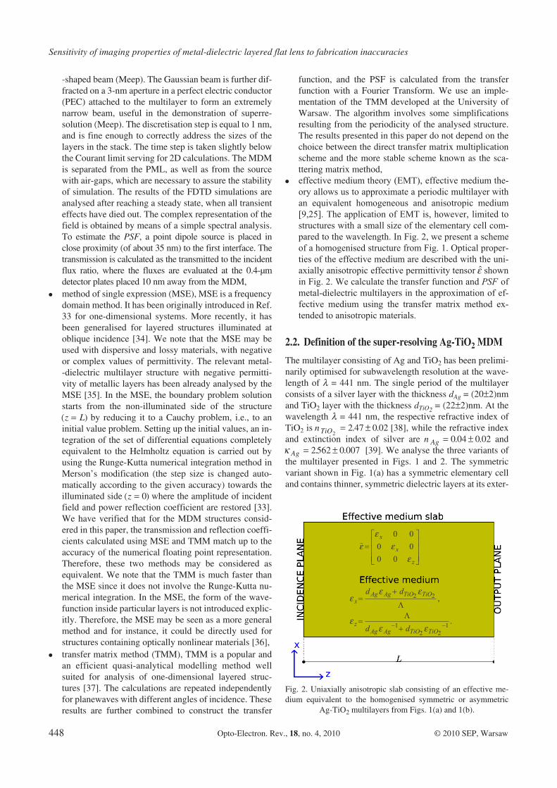
2.3. Optical properties of MDM structureIn Fig. 3(a) we show the dependence of the transfer function ofthe symmetrical multilayer on the number of periods N calcu−lated with the TMM. Clearly, a broad range of spatial frequen−cies corresponding to evanescent waves ( )k kx 0 1� , which isnecessary to increase the resolution beyond the diffractionlimit, is transmitted through the structure. Due to absorption,both the amplitude of the TF as well as the spatial frequencybandwidth rapidly drop with the increase in the number of pe−riods N . The same TF, including the information on the phasemodulation is presented in Fig. 3(b) for N �1015 20, , . Fi−gures 3(c) and 3(d) show the PSF calculated with the TMMand the FDTD methods, respectively. Notably, these resultsare in good agreement, and the small difference may be attri−buted to the location of the source and the detector at a certaindistance from the MDM in the FDTD simulation, as well as tothe finite size of the dipole source.
Opto−Electron. Rev., 18, no. 4, 2010 R. Kotyński 449
Fig. 3. (a) Dependence of a transfer function of symmetric multilayer on the number of periods N (calculated with TMM), (b) transfer func−tion, (c) point spread function of a multilayer with N �10 15, and 20 layers calculated with TMM (amplitude or intensity is drawn with a solid
line, and phase with a dashed line), and (d) point spread function of a multilayer with N �10 15, and 20 layers calculated with FDTD.
The resolution attainable with the MDM may be deter−mined from the width and shape of the point spread function[Figs. 3(c) and 3(d)]. The width of PSF is in the order of � 10and it broadens rather slowly with the number of periods.
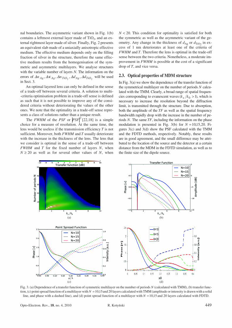
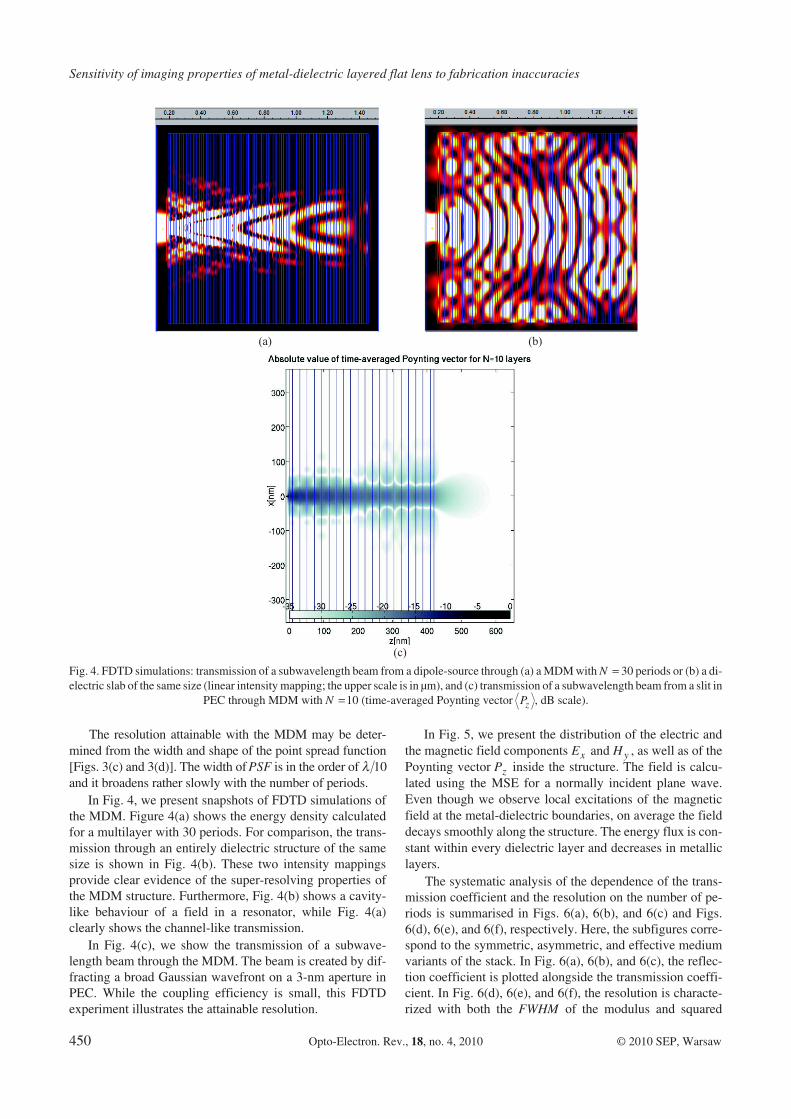
In Fig. 4, we present snapshots of FDTD simulations ofthe MDM. Figure 4(a) shows the energy density calculatedfor a multilayer with 30 periods. For comparison, the trans−mission through an entirely dielectric structure of the samesize is shown in Fig. 4(b). These two intensity mappingsprovide clear evidence of the super−resolving properties ofthe MDM structure. Furthermore, Fig. 4(b) shows a cavity−like behaviour of a field in a resonator, while Fig. 4(a)clearly shows the channel−like transmission.
In Fig. 4(c), we show the transmission of a subwave−length beam through the MDM. The beam is created by dif−fracting a broad Gaussian wavefront on a 3−nm aperture inPEC. While the coupling efficiency is small, this FDTDexperiment illustrates the attainable resolution.
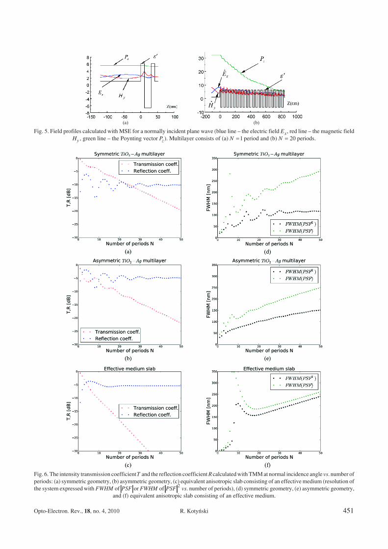
In Fig. 5, we present the distribution of the electric andthe magnetic field components Ex and Hy , as well as of thePoynting vector Pz inside the structure. The field is calcu−lated using the MSE for a normally incident plane wave.Even though we observe local excitations of the magneticfield at the metal−dielectric boundaries, on average the fielddecays smoothly along the structure. The energy flux is con−stant within every dielectric layer and decreases in metalliclayers.
The systematic analysis of the dependence of the trans−mission coefficient and the resolution on the number of pe−riods is summarised in Figs. 6(a), 6(b), and 6(c) and Figs.6(d), 6(e), and 6(f), respectively. Here, the subfigures corre−spond to the symmetric, asymmetric, and effective mediumvariants of the stack. In Fig. 6(a), 6(b), and 6(c), the reflec−tion coefficient is plotted alongside the transmission coeffi−cient. In Fig. 6(d), 6(e), and 6(f), the resolution is characte−rized with both the FWHM of the modulus and squared
Sensitivity of imaging properties of metal−dielectric layered flat lens to fabrication inaccuracies
450 Opto−Electron. Rev., 18, no. 4, 2010 © 2010 SEP, Warsaw
Fig. 4. FDTD simulations: transmission of a subwavelength beam from a dipole−source through (a) a MDM with N � 30 periods or (b) a di−electric slab of the same size (linear intensity mapping; the upper scale is in μm), and (c) transmission of a subwavelength beam from a slit in
PEC through MDM with N �10 (time−averaged Poynting vector Pz , dB scale).
Opto−Electron. Rev., 18, no. 4, 2010 R. Kotyński 451
Fig. 5. Field profiles calculated with MSE for a normally incident plane wave (blue line – the electric field Ex, red line – the magnetic fieldHy , green line – the Poynting vector Pz ). Multilayer consists of (a) N �1 period and (b) N � 20 periods.
Fig. 6. The intensity transmission coefficientT and the reflection coefficient R calculated with TMM at normal incidence angle vs. number ofperiods: (a) symmetric geometry, (b) asymmetric geometry, (c) equivalent anisotropic slab consisting of an effective medium (resolution ofthe system expressed with FWHM of PSF or FWHM of PSF 2 vs. number of periods), (d) symmetric geometry, (e) asymmetric geometry,
and (f) equivalent anisotropic slab consisting of an effective medium.
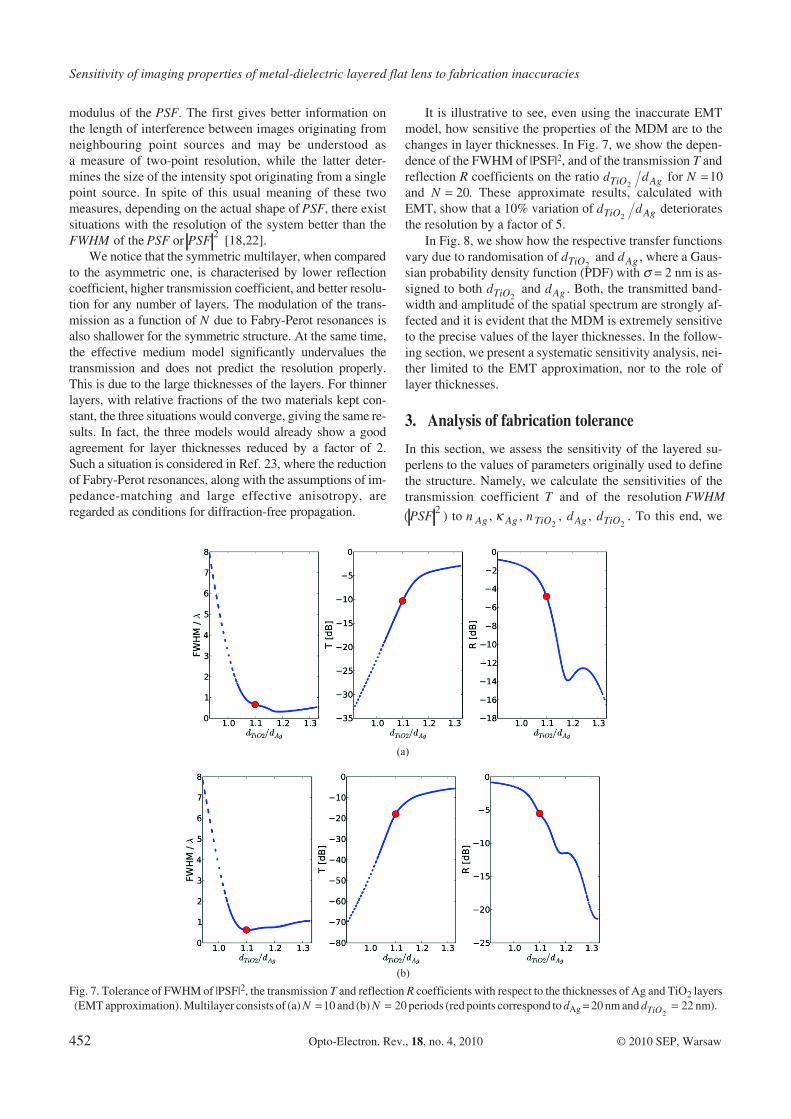
modulus of the PSF. The first gives better information onthe length of interference between images originating fromneighbouring point sources and may be understood asa measure of two−point resolution, while the latter deter−mines the size of the intensity spot originating from a singlepoint source. In spite of this usual meaning of these twomeasures, depending on the actual shape of PSF, there existsituations with the resolution of the system better than theFWHM of the PSF or PSF 2 [18,22].
We notice that the symmetric multilayer, when comparedto the asymmetric one, is characterised by lower reflectioncoefficient, higher transmission coefficient, and better resolu−tion for any number of layers. The modulation of the trans−mission as a function of N due to Fabry−Perot resonances isalso shallower for the symmetric structure. At the same time,the effective medium model significantly undervalues thetransmission and does not predict the resolution properly.This is due to the large thicknesses of the layers. For thinnerlayers, with relative fractions of the two materials kept con−stant, the three situations would converge, giving the same re−sults. In fact, the three models would already show a goodagreement for layer thicknesses reduced by a factor of 2.Such a situation is considered in Ref. 23, where the reductionof Fabry−Perot resonances, along with the assumptions of im−pedance−matching and large effective anisotropy, areregarded as conditions for diffraction−free propagation.
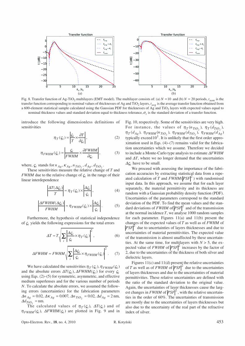
It is illustrative to see, even using the inaccurate EMTmodel, how sensitive the properties of the MDM are to thechanges in layer thicknesses. In Fig. 7, we show the depen−dence of the FWHM of |PSF|2, and of the transmission T andreflection R coefficients on the ratio d dTiO Ag2
for N �10and N � 20. These approximate results, calculated withEMT, show that a 10% variation of d dTiO Ag2
deterioratesthe resolution by a factor of 5.
In Fig. 8, we show how the respective transfer functionsvary due to randomisation of dTiO2
and dAg , where a Gaus−sian probability density function (PDF) with � = 2 nm is as−signed to both dTiO2
and dAg . Both, the transmitted band−width and amplitude of the spatial spectrum are strongly af−fected and it is evident that the MDM is extremely sensitiveto the precise values of the layer thicknesses. In the follow−ing section, we present a systematic sensitivity analysis, nei−ther limited to the EMT approximation, nor to the role oflayer thicknesses.
3. Analysis of fabrication tolerance
In this section, we assess the sensitivity of the layered su−perlens to the values of parameters originally used to definethe structure. Namely, we calculate the sensitivities of thetransmission coefficient T and of the resolution FWHM
( )PSF 2 to n Ag , � Ag , n TiO2, dAg , dTiO2
. To this end, we
Sensitivity of imaging properties of metal−dielectric layered flat lens to fabrication inaccuracies
452 Opto−Electron. Rev., 18, no. 4, 2010 © 2010 SEP, Warsaw
Fig. 7. Tolerance of FWHM of |PSF|2, the transmission T and reflection R coefficients with respect to the thicknesses of Ag and TiO2 layers(EMT approximation). Multilayer consists of (a) N �10 and (b) N � 20 periods (red points correspond to dAg = 20 nm and dTiO2
22� nm).
introduce the following dimensionless definitions ofsensitivities
�
T ii
iT
T( ) � , (2)
�
FWHM ii
iFWHM
FWHM( ) � , (3)
where, i stands for n Ag ,� Ag , n TiO2, dAg , dTiO2
.These sensitivities measure the relative change of T and
FWHM due to the relative change of i in the range of theirlinear interdependence
� � �T
Ti
T ii
i
( )( )
�
, (4)
� � �FWHM
FWHMi
FWHM ii
i
( )( )
�
. (5)
Furthermore, the hypothesis of statistical independenceof i yields the following expressions for the total errors
��
T T i
iT i
i
�
� ( )2
, (6)
��
FWHM FWHM i
iFWHM i
i
�
� ( )2
. (7)
We have calculated the sensitivities � � T i FWHM i( ), ( )and the absolute errors � �T FWHMi i( ), ( ) for every iusing Eqs. (2)–(5) for symmetric, asymmetric, and effectivemedium superlenses and for the various number of periodsN . To calculate the absolute errors, we assumed the follow−ing errors (uncertainties) for the fabrication parameters�n Ag � 0 02. , �� Ag � 0 007. , �n TiO2
0 02� . , �dAg � 2 nm,�dTiO2
� nm.The calculated values of � T i( ), �T i( ) and of
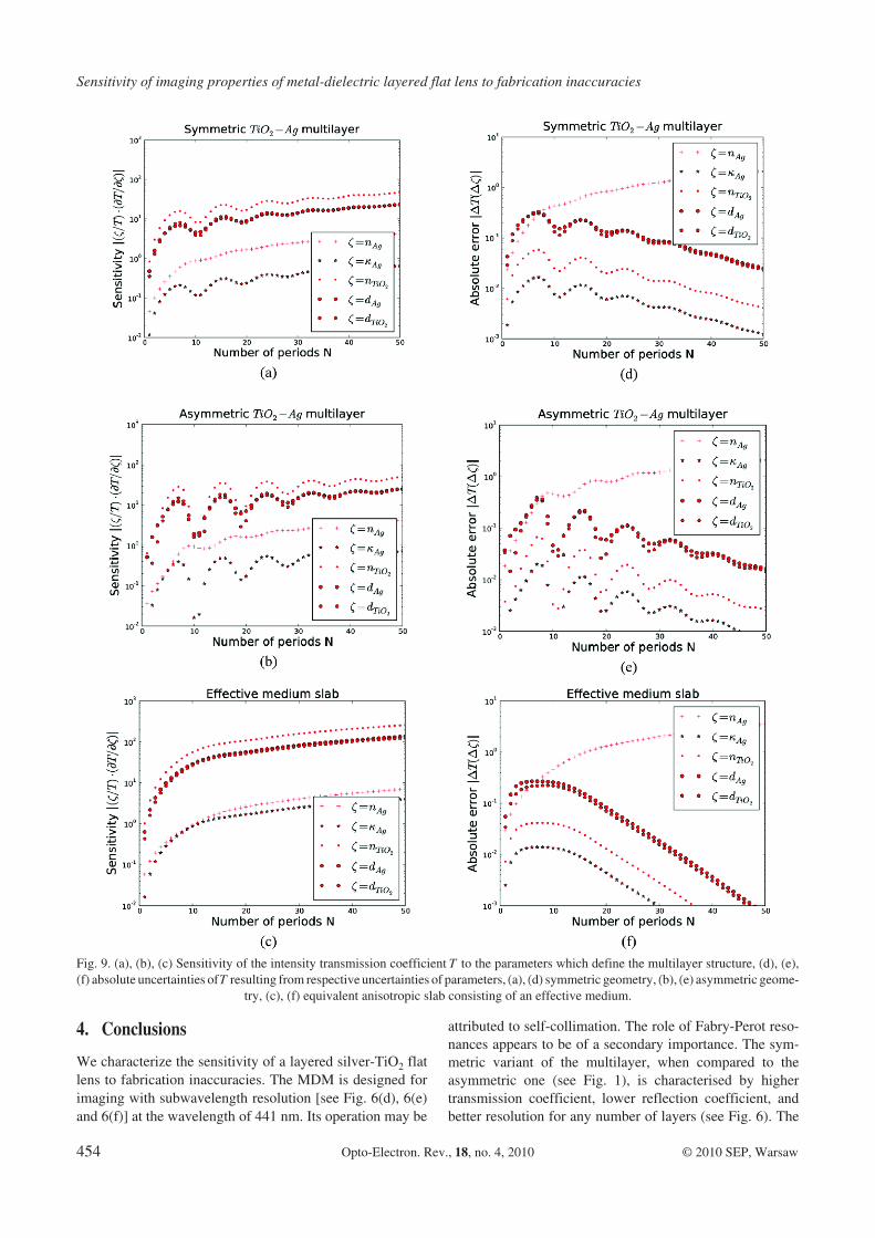
� FWHM i( ), �FWHM i( ) are plotted in Fig. 9 and in
Fig. 10, respectively. Some of the sensitivities are very high.For instance, the values of � T TiOn( )
2, � T TiOd( )
2,
� T Agd( ), � FWHM TiOn( )2
, � FWHM TiOd( )2
, � FWHM Agd( )typically exceed101. It is unlikely that the first order appro−ximation used in Eqs. (4)–(7) remains valid for the fabrica−tion uncertainties which we assume. Therefore we decidedto include a Monte−Carlo type analysis to estimate �FWHMand �T, where we no longer demand that the uncertainties�i have to be small.
We proceed with assessing the importance of the fabri−cation accuracies by extracting statistical data from a repe−ated calculation of T and FWHM PSF( )2 with randomisedinput data. In this approach, we assume that for each layerseparately, the material permittivity and its thickness arerandom with a Gaussian probability density function (PDF).Uncertainties of the parameters correspond to the standarddeviation of the PDF. To find the mean values and the stan−dard deviations of FWHM of PSF 2 and of the transmissionat the normal incidence T, we analyse 1000 random samplesfor each parameter. Figures 11(a) and 11(b) present thechanges of the expected values of T as well as of FWHM ofPSF 2 due to uncertainties of layers thicknesses and due touncertainties of material permittivities. The expected valueof the transmission is almost unaffected by these uncertain−ties. At the same time, for multilayers with N > 5, the ex−pected value of FWHM of PSF 2 increases by the factor of2, due to the uncertainties of the thickness of both silver anddielectric layers.
Figures 11(c) and 11(d) present the relative uncertaintiesof T as well as of FWHM of PSF 2 due to the uncertaintiesof layers thicknesses and due to the uncertainties of materialpermittivities. These relative uncertainties are defined withthe ratio of the standard deviation to the original value.Again, the uncertainties of layer thicknesses cause the larg−est changes in FWHM of PSF 2 , with the relative uncertain−ties in the order of 60%. The uncertainties of transmissionare mostly due to the uncertainties of layers thicknesses butalso due to the uncertainty of the real part of the refractiveindex of silver.
Opto−Electron. Rev., 18, no. 4, 2010 R. Kotyński 453
Fig. 8. Transfer function of Ag−TiO2 multilayers (EMT model). The multilayer consists of: (a) N �10 and (b) N � 20 periods, tnom is thetransfer function corresponding to nominal values of thicknesses of Ag and TiO2 layers, tavg is the average transfer function obtained froma 600−element statistical sample calculated using the Gaussian PDF for thicknesses of Ag and TiO2 layers with expected values equal to
nominal thickness values and standard deviation equal to thickness tolerance,� t is the standard deviation of a transfer function.
4. Conclusions
We characterize the sensitivity of a layered silver−TiO2 flatlens to fabrication inaccuracies. The MDM is designed forimaging with subwavelength resolution [see Fig. 6(d), 6(e)and 6(f)] at the wavelength of 441 nm. Its operation may be
attributed to self−collimation. The role of Fabry−Perot reso−nances appears to be of a secondary importance. The sym−metric variant of the multilayer, when compared to theasymmetric one (see Fig. 1), is characterised by highertransmission coefficient, lower reflection coefficient, andbetter resolution for any number of layers (see Fig. 6). The
Sensitivity of imaging properties of metal−dielectric layered flat lens to fabrication inaccuracies
454 Opto−Electron. Rev., 18, no. 4, 2010 © 2010 SEP, Warsaw
Fig. 9. (a), (b), (c) Sensitivity of the intensity transmission coefficient T to the parameters which define the multilayer structure, (d), (e),(f) absolute uncertainties ofT resulting from respective uncertainties of parameters, (a), (d) symmetric geometry, (b), (e) asymmetric geome−
try, (c), (f) equivalent anisotropic slab consisting of an effective medium.
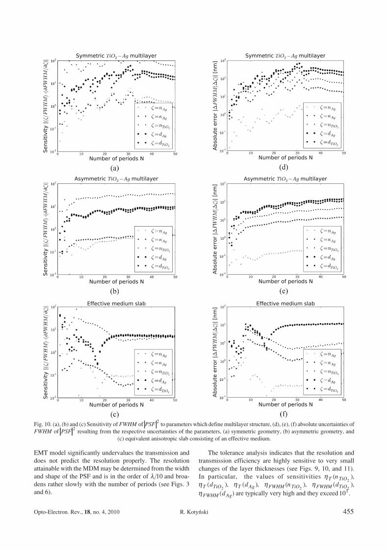
EMT model significantly undervalues the transmission anddoes not predict the resolution properly. The resolutionattainable with the MDM may be determined from the widthand shape of the PSF and is in the order of � 10 and broa−dens rather slowly with the number of periods (see Figs. 3and 6).
The tolerance analysis indicates that the resolution andtransmission efficiency are highly sensitive to very smallchanges of the layer thicknesses (see Figs. 9, 10, and 11).In particular, the values of sensitivities � T TiOn( )
2,
� T TiOd( )2
, � T Agd( ), � FWHM TiOn( )2
, � FWHM TiOd( )2
,� FWHM Agd( ) are typically very high and they exceed 101.
Opto−Electron. Rev., 18, no. 4, 2010 R. Kotyński 455
Fig. 10. (a), (b) and (c) Sensitivity of FWHM of PSF 2 to parameters which define multilayer structure, (d), (e), (f) absolute uncertainties ofFWHM of PSF 2 resulting from the respective uncertainties of the parameters, (a) symmetric geometry, (b) asymmetric geometry, and
(c) equivalent anisotropic slab consisting of an effective medium.
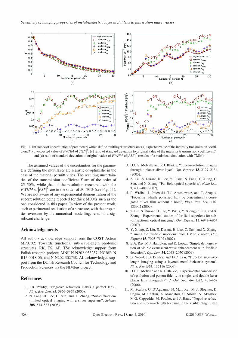
The assumed values of the uncertainties for the parame−ters defining the multilayer are realistic or optimistic in thecase of the material permittivities. The resulting uncertain−ties of the transmission coefficient T are of the order of25–50%, while that of the resolution measured with theFWHM of PSF 2 are in the order of 50–70% (see Fig. 11).We are not aware of any experimental demonstration of thesuperresolution being reported for thick MDMs such as theone considered in this paper. In view of the present work,such experimental realisation of a structure, with the proper−ties overseen by the numerical modelling, remains a sig−nificant challenge.
Acknowledgements
All authors acknowledge support from the COST ActionMP0702: Towards functional sub−wavelength photonicstructures. RK, TS, AP, TSz acknowledge support fromPolish research projects MNiI N N202 033237, NCBiR NR15 0018 06, and N N202 302738. AL acknowledges sup−port from the Danish Research Council for Technology andProduction Sciences via the NIMbus project.
References
1. J.B. Pendry, “Negative refraction makes a perfect lens”,Phys. Rev. Lett. 85, 3966–3969 (2000).
2. N. Fang, H. Lee, C. Sun, and X. Zhang, “Sub−diffraction−−limited optical imaging with a silver superlens”, Science308, 534–537 (2005).
3. D.O.S. Melville and R.J. Blaikie, “Super−resolution imagingthrough a planar silver layer”, Opt. Express 13, 2127–2134(2005).
4. Z. Liu, S. Durant, H. Lee, Y. Pikus, N. Fang, Y. Xiong, C.Sun, and X. Zhang, “Far−field optical superlens”, Nano Lett.7, 403–408 (2007).
5. P. Wróbel, J. Pniewski, T.J. Antosiewicz, and T. Szoplik,“Focusing radially polarized light by concentrically corru−gated silver film without a hole”, Phys. Rev. Lett. 102,183902 (2009).
6. Z. Liu, S. Durant, H. Lee, Y. Pikus, Y. Xiong, C. Sun, and X.Zhang, “Experimental studies of far−field superlens for sub−−diffractional optical imaging”, Opt. Express 15, 6947–6954(2007).
7. Y. Xiong, Z. Liu, S. Durant, H. Lee, C. Sun, and X. Zhang,“Tuning the far−field superlens: from UV to visible”, Opt.Express 15, 7095–7102 (2007).
8. E.A. Ray, M.J. Hampton, and R. Lopez, “Simple demonstra−tion of visible evanescent−wave enhancement with far−fielddetection”, Opt. Lett. 34, 2048–2050 (2009).
9. B. Wood, J.B. Pendry, and D.P. Tsai, “Directed subwave−length imaging using a layered metal−dielectric system”,Phys. Rev. B74, 115116 (2006).
10. D.O.S. Melville and R.J. Blaikie, “Experimental comparisonof resolution and pattern fidelity in single− and double−layerplanar lens lithography”, J. Opt. Soc. Am. B23, 461–467(2006).
11. M. Scalora, G. D’Aguanno, N. Mattiucci, M. J. Bloemer, D.Ceglia, M. Centini, A. Mandatori, C. Sibilia, N. Akozbek,M.G. Cappeddu, M. Fowler, and J. Haus, “Negative refrac−tion and sub−wavelength focusing in the visible range using
Sensitivity of imaging properties of metal−dielectric layered flat lens to fabrication inaccuracies
456 Opto−Electron. Rev., 18, no. 4, 2010 © 2010 SEP, Warsaw
Fig. 11. Influence of uncertainties of parameters which define multilayer structure on: (a) expected value of the intensity transmission coeffi−cient T , (b) expected value of FWHM of PSF 2 , (c) ratio of standard deviation to original value of the intensity transmission coefficient T ,
and (d) ratio of standard deviation to original value of FWHM of PSF 2 (results of a statistical simulation with TMM).
transparent metallo−dielectric stacks”, Opt. Express 15,508–523 (2007).
12. X. Li, S. He, and Y. Jin, “Subwavelength focusing witha multilayered Fabry−Perot structure at optical frequencies”,Phys. Rev. B75, 045103 (2007).
13. D. de Ceglia, M.A. Vincenti, M.G. Cappeddu, M. Centini, N.Akozbek, A. DOrazio, J. Haus, M.J. Bloemer, and M.Scalora, “Tailoring metallodielectric structures for super−resolution and superguiding applications in the visible andnear−IR ranges”, Phys. Rev. A77, 033848 (2008).
14. M. Conforti, M. Guasoni, and C. De Angelis, “Subwave−length diffraction management”, Opt. Lett. 33, 2662–2664(2008).
15. C.P. Moore, M.D. Arnold, P.J. Bones, and R.J. Blaikie,“Analysis and comparison of simulation techniques for sil−ver superlenses”, Proc. Int. Conf. Nanoscience and Nano−technology, ICONN 2008, 210–213 (2008).
16. C.P. Moore, M.D. Arnold, P.J. Bones, and R.J. Blaikie, “Im−age fidelity for single−layer and multi−layer silver super−lenses”, J. Opt. Soc. Am. A25, 911–918 (2008).
17. C.P. Moore, R.J. Blaikie, and M.D. Arnold, “An improvedtransfer−matrix model for optical superlenses”, Opt. Express17, 14260–14269 (2009).
18. R. Kotynski and T. Stefaniuk, “Comparison of imaging withsub−wavelength resolution in the canalization and resonanttunnelling regimes”, J. Opt. A−Pure Appl. Op. 11, 015001(2009).
19. N. Mattiucci, G. D’Aguanno, M. Scalora, M.J. Bloemer, andC. Sibilia, “Transmission function properties for multi−lay−ered structures: Application to superresolution”, Opt. Ex−press 17, 17517–17529 (2009).
20. Q.M. Quan, S.L. Zhu, and R.P. Wang, “Refraction in thefixed direction at the surface of dielectric/silver superlatti−ce”, Phys. Lett. A359, 547–549 (2006).
21. X. Li and F. Zhuang, “Multilayered structures with high sub−wavelength resolution based on the metal−dielectric compos−ites”, J. Opt. Soc. Am. A26, 2521–2525 (2009).
22. R. Kotyński and T. Stefaniuk, “Multiscale analysis of subwa−velength imaging with metal−dielectric multilayers”, Opt.Lett. 35, 1133–1135 (2010).
23. R. Kotyński, T. Stefaniuk, and A. Pastuszczak, “Sub−wave−length diffraction−free imaging with low−loss metal−dielec−tric multilayers”, ArXiv:1002.0658. (submitted to J. Appl.Phys. A, 2010)
24. P.A. Belov, C. Simovski, and P. Ikonen, “Canalization ofsubwavelength images by electro−magnetic crystals”, Phys.Rev. B71, 193105 (2005).
25. P.A. Belov and Y. Hao, “Subwavelength imaging at opticalfrequencies using a transmission device formed by a periodic
layered metal−dielectric structure operating in the canaliza−tion regime”, Phys. Rev. B73, 113110 (2006).
26. M.A. Vincenti, A. D'Orazio, M.G. Cappeddu, N. Akozbek,M.J. Bloemer, and M. Scalora, “Semiconductor−based super−lens for subwavelength resolution below the diffraction limitat extreme ultraviolet frequencies”, J. Appl. Phys. 105,103103 (2009).
27. J.W. Goodman, Introduction to Fourier Optics, Roberts &Co Publ., 3rd ed., 2005.
28. B. Saleh and M. Teich, Fundamentals of Photonics, JohnWiley & Sons, Inc, 2nd ed., 2007.
29. R. Kotyński, “Fourier optics approach to imaging with sub−−wavelength resolution through metal−dielectric multila−yers”, Opto−Electron. Rev. 18, 366–375 (2010), (in press,arXiv 1006.3669).
30. A. Taflove and S.C. Hagness, Computational Electrodynam−ics: The Finite−Difference Time−Domain Method, ArtecHouse Inc., Boston, 2nd ed., 2000.
31. A. Farjadpour, D. Roundy, A. Rodriguez, M. Ibanescu, P.Bermel, J.D. Joannopoulos, S.G. Johnson, and G. Burr, “Im−proving accuracy by subpixel smoothing in FDTD”, Opt.Lett. 31, 2972–2974 (2006).
32. http://www.photond.com/products/crystalwave.htm (anoverview of the computation engine implemented in theCrystal Wave tool by the Photon Design Ltd., Oxford).
33. H.V. Baghdasaryan and T.M. Knyazyan, “Problem of planeEM wave self−action in multilayer structure: an exact solu−tion”, Opt. Quant. Electron. 31, 1059–1072 (1999).
34. H.V. Baghdasaryan, T.M. Knyazyan, T.H. Baghdasaryan,and G.G. Eyramjyan, “Development of the method of singleexpression (MSE) for analysis of plane wave oblique inci−dence on multilayer structures having complex permittivityand permeability”, Proc. ICTON’2008, Vol. 1, 250–254(2008).
35. H.V. Baghdasaryan, T.M. Knyazyan, and G.G. Eyramjyan,“Electrodynamical analysis of a transmittive metal−dielectricmicrostructure by the method of single expression”, Proc.European Microwave Association 4, 76–81 (2008).
36. H.V. Baghdasaryan and T.M. Knyazyan, “Modelling ofstrongly nonlinear sinusoidal Bragg gratings by the methodof single expression”, Opt. Quant. Electron. 32, 869–883(2000).
37. P. Markos and C. M. Soukoulis, Wave Propagation. FromElectrons to Photonic Crystals and Left−handed Materials,Princeton University Press, Princeton and Oxford, 2008.
38. O. Duyar, F. Placido, and H.Z. Durusoy, “Optimization ofTiO2 films prepared by reactive electron beam evaporationof Ti3O5”, J. Phys. D. Appl. Phys. 41, 095307 (2008).
39. P. Johnson and R. Christy, “Optical constants of the noblemetals”, Phys. Rev. B6, 4370–4379 (1972).
Opto−Electron. Rev., 18, no. 4, 2010 R. Kotyński 457
Copyright © 2022 FDOKUMEN