140W ACF+GaN PD3.0 Adapter EVB User Guide - Transphorm
31
140W ACF+GaN PD3.0 Adapter EVB User Guide 140W ACF+GaN PD3.0 Adapter EVB Page 1 of 31 12/08/2021 Revision 1.0 www.diodes.com Table of Contents Chapter 1 Summary ......................................................................................................................3 1.1 General Description ......................................................................................................................... 3 1.2 Key Features .................................................................................................................................... 3 1.2.1 System Key Features ................................................................................................................................................ 3 1.2.2 AP3306 Key Features ............................................................................................................................................... 3 1.2.3 APR340 Key Features ............................................................................................................................................... 3 1.2.4 AP43771V Key Feature............................................................................................................................................. 3 1.3 Applications .................................................................................................................................... 3 1.4 Main Power Specifications ............................................................................................................... 3 1.5 Evaluation Board Picture .................................................................................................................. 3 Chapter 2 Power Supply Specification............................................................................................4 2.1 Specification and Test Results .......................................................................................................... 4 Chapter 3 Schematic .....................................................................................................................5 3.1 Board Schematic .............................................................................................................................. 5 3.2 Bill of Material (BOM) ...................................................................................................................... 7 3.3 PFC Inductance, Transformer Design ................................................................................................ 9 3.3.1 PFC Inductance......................................................................................................................................................... 9 3.3.2 ACF Transformer .................................................................................................................................................... 10 3.4 Schematics Description .................................................................................................................. 11 3.4.1 AC Input Circuit & Differential Filter ...................................................................................................................... 11 3.4.2 UCC28056 PFC Controller ...................................................................................................................................... 11 3.4.3 AP3306 PWM Controller ........................................................................................................................................ 11 3.4.4 APR340 Synchronous Rectification (SR) MOSFET Driver ....................................................................................... 11 3.4.5 AP43771V PD 3.0 Decoder & Protection on/off N MOSFET and Interface to Power Devices .............................. 11 Chapter 4 The Evaluation Board (EVB) Connections ..................................................................... 12 4.1 EVB PCB Layout ............................................................................................................................. 12 4.2 Quick Start Guide before Connection.............................................................................................. 14 4.3 Connection with E-Load ................................................................................................................. 15 Chapter 5 Testing the Evaluation Board ...................................................................................... 16 5.1 Input & Output Characteristics ....................................................................................................... 16 5.1.1 Input Standby Power ............................................................................................................................................. 16 5.1.2 Multiple Output Efficiency at Different AC Line Input Voltage ............................................................................. 16 5.1.3 Efficiency vs. AC Line Input Voltage ....................................................................................................................... 17 5.1.4 Total Harmonic Distortion (THD) and Power Factor Correction (PFC) .................................................................. 18 5.1.5 Multiple Output Average Efficiency at Different Loading ..................................................................................... 19
-
Upload
khangminh22 -
Category
Documents
-
view
0 -
download
0
Transcript of 140W ACF+GaN PD3.0 Adapter EVB User Guide - Transphorm

140W ACF+GaN PD3.0 Adapter EVB User Guide
140W ACF+GaN PD3.0 Adapter EVB Page 1 of 31 12/08/2021 Revision 1.0 www.diodes.com
Table of Contents
Chapter 1 Summary ......................................................................................................................3
1.1 General Description ......................................................................................................................... 3
1.2 Key Features .................................................................................................................................... 3 1.2.1 System Key Features ................................................................................................................................................ 3 1.2.2 AP3306 Key Features ............................................................................................................................................... 3 1.2.3 APR340 Key Features ............................................................................................................................................... 3 1.2.4 AP43771V Key Feature............................................................................................................................................. 3
1.3 Applications .................................................................................................................................... 3
1.4 Main Power Specifications ............................................................................................................... 3
1.5 Evaluation Board Picture .................................................................................................................. 3
Chapter 2 Power Supply Specification............................................................................................4
2.1 Specification and Test Results .......................................................................................................... 4
Chapter 3 Schematic .....................................................................................................................5
3.1 Board Schematic .............................................................................................................................. 5
3.2 Bill of Material (BOM) ...................................................................................................................... 7
3.3 PFC Inductance, Transformer Design ................................................................................................ 9 3.3.1 PFC Inductance......................................................................................................................................................... 9 3.3.2 ACF Transformer .................................................................................................................................................... 10
3.4 Schematics Description .................................................................................................................. 11 3.4.1 AC Input Circuit & Differential Filter ...................................................................................................................... 11 3.4.2 UCC28056 PFC Controller ...................................................................................................................................... 11 3.4.3 AP3306 PWM Controller ........................................................................................................................................ 11 3.4.4 APR340 Synchronous Rectification (SR) MOSFET Driver ....................................................................................... 11 3.4.5 AP43771V PD 3.0 Decoder & Protection on/off N MOSFET and Interface to Power Devices .............................. 11
Chapter 4 The Evaluation Board (EVB) Connections ..................................................................... 12
4.1 EVB PCB Layout ............................................................................................................................. 12
4.2 Quick Start Guide before Connection.............................................................................................. 14
4.3 Connection with E-Load ................................................................................................................. 15
Chapter 5 Testing the Evaluation Board ...................................................................................... 16
5.1 Input & Output Characteristics ....................................................................................................... 16 5.1.1 Input Standby Power ............................................................................................................................................. 16 5.1.2 Multiple Output Efficiency at Different AC Line Input Voltage ............................................................................. 16 5.1.3 Efficiency vs. AC Line Input Voltage ....................................................................................................................... 17 5.1.4 Total Harmonic Distortion (THD) and Power Factor Correction (PFC) .................................................................. 18 5.1.5 Multiple Output Average Efficiency at Different Loading ..................................................................................... 19

140W ACF+GaN PD3.0 Adapter EVB User Guide
140W ACF+GaN PD3.0 Adapter EVB Page 2 of 31 12/08/2021 Revision 1.0 www.diodes.com
5.2 Key Performance Waveforms ......................................................................................................... 20 5.2.1 System Start-up Time ............................................................................................................................................. 20 5.2.2 PFC Start-up ........................................................................................................................................................... 20 5.2.3 Line Voltage and Line Current................................................................................................................................ 21 5.2.4 Switching Transistor Voltage Stress ....................................................................................................................... 22 5.2.5 System Output Ripple & Noise with the Cable ...................................................................................................... 24 5.2.6 Dynamic load.......................................................................................................................................................... 26 5.2.7 Output Voltage Transition Time ............................................................................................................................ 28 5.2.8 Thermal Testing ..................................................................................................................................................... 29
5.3 EMI (Conduction) Testing ............................................................................................................... 30 5.3.1 115VAC testing results ........................................................................................................................................... 30 5.3.2 230VAC testing results ........................................................................................................................................... 30

140W ACF+GaN PD3.0 Adapter EVB User Guide
140W ACF+GaN PD3.0 Adapter EVB Page 3 of 31 12/08/2021 Revision 1.0 www.diodes.com
Chapter 1 Summary
1.1 General Description
The 140W ACF PD3.0 Evaluation Board is composed of four main controllers, UCC28056, AP3306, APR340 and AP43771V. UCC28056B is transition mode boost PFC controller. AP3306 is a highly integrated Active Clamp Flyback (ACF) controller that is optimally designed for offline power supply to meet ultra-low standby power, high power density, and comprehensive protection requirements. The APR340 is a secondary side Synchronous Rectification (SR) Controller. The AP43771V, a protocol decoder in charge of matching the associated charger capacity and request by an attached Type C-equipped device under charged (DUC), regulates the feedback network of the charger to fulfill voltage and current requirements from DUC. In addition, Gallium Nitride (GaN) FET is employed to further improve the efficiency and thermal performance.
1.2 Key Features
1.2.1 System Key Features
• Optimal system implementation for high-efficiency
BOM-optimized High Power Density Chargers
• Diodes Patented ACF Topology Implementation for
Critical Efficiency Improvement Approaches
• High-Voltage Startup low standby power
• Meets DOE VI and COC Tier 2 Efficiency
Requirements
• USB Type-C Output Cable - Support the Maximum Output of 140W PD 3.0 Function
1.2.2 AP3306 Key Features
• Active Clamp Flyback Topology with Recycled Leakage Energy and Zero Voltage Switching Functions
• High-Voltage Startup
• Embedded VCC LDO for VCCL pin to Guarantee Wide Range Output Voltage
• Constant, Low Output Current in Output Short Situation
• Non-Audible-Noise Quasi-Resonant Control
• Soft Start During Startup Process
• Frequency Fold Back for High Average Efficiency
• Secondary Winding Short Protection with FOCP
• Frequency Dithering for Reducing EMI
• X-CAP Discharge Function
• Useful Pin fault protection: SENSE Pin Floating Protection/ FB/Opto-Coupler Open/Short Protection
• Comprehensive System Protection Feature: VOVP/OLP/BNO/SOVP/SUVP
1.2.3 APR340 Key Features
• Synchronous Rectification Works with DCM / QR / ACF operation modes
• Eliminate Resonant Ringing Interference
• Fewest External Components used
1.2.4 AP43771V Key Feature
• Support USB PD Rev 3.0 V1.2
• USB-IF PD3.0/PPS Certified TID 4312
• Qualcomm QC5 Certified: QC20201127203
• MTP for System Configuration
• OTP for Main Firmware
• Operating Voltage Range: 3.3V to 21V
• Built-In Regulator for CV and CC Control
• Programmable OVP/UVP/OCP/OTP
• Support Power Saving Mode
• External N -MOSFET Control for VBUS Power Delivery
• Support e-Marker Cable Detection
• W-DFN3030-14
1.3 Applications
• Quick Charger with full power range of PD3.0
1.4 Main Power Specifications
Parameter Value
Input Voltage 90VAC to 264VAC
Input standby power < 100mW
Main Output (Vo / Io) PDO: 5V/3A, 9V/3A, 15V/3A, 20V/7A,
Efficiency Comply with CoC version 5 tier-2
Max. Output Power 140W (at PDO 20V/7A)
Protections OCP, OVP, UVP, OLP, OTP, SCP
Dimensions PCB: 125*55*30mm
1.5 Evaluation Board Picture
Figure 1: Top View
Figure 2: Bottom View

140W ACF+GaN PD3.0 Adapter EVB User Guide
140W ACF+GaN PD3.0 Adapter EVB Page 4 of 31 12/08/2021 Revision 1.0 www.diodes.com
Chapter 2 Power Supply Specification
2.1 Specification and Test Results
Parameter Value Test Summary
Input Voltage / Frequency 90VAC to 264VAC / 50Hz or 60Hz Test Condition
Input Current <2ARMS
Standby Power <100mW; load disconnected PASS, 42.7mW @230VAC/50Hz
5V/3A Average Efficiency CoC Version 5, Tier2 Efficiency >81.84% PASS, 89.75% @115VAC/60Hz
89.92% @230VAC/50Hz
5V/0.3A Efficiency (10% Load) CoC Version 5, Tier2 Efficiency >72.48% PASS, 86.69% @115VAC/60Hz
85.59% @230VAC/50Hz
9V/3A Average Efficiency CoC Version 5, Tier2 Efficiency >87.30% PASS, 91.81% @115VAC/60Hz
92.53% @230VAC/50Hz
9V/0.3A Efficiency (10% Load) CoC Version 5, Tier2 Efficiency >77.30% PASS, 88.70% @115VAC/60Hz
89.10% @230VAC/50Hz
15V/3A Average Efficiency CoC Version 5, Tier2 Efficiency >88.85% PASS, 92.11% @115VAC/60Hz
93.12% @230VAC/50Hz
15V/0.3A Efficiency (10% Load) CoC Version 5, Tier2 Efficiency >78.85% PASS, 89.20% @115VAC/60Hz
89.04% @230VAC/50Hz
20V/7A Average Efficiency CoC Version 5, Tier2 Efficiency >88.85% PASS, 91.38% @115VAC/60Hz
92.48% @230VAC/50Hz
20V/0.7A Efficiency (10% Load) CoC Version 5, Tier2 Efficiency >78.85% PASS, 88.20% @115VAC/60Hz
89.43% @230VAC/50Hz
Output Voltage Regulation Tolerance
+/- 5% PASS,
Power Factor >0.9; when output power is over 70W PASS, 0.9822 @115 VAC /60Hz
0.9271 @230 VAC /50Hz
THD <20%; when output power is over 70W PASS, 15.9% @115 VAC /60Hz
15.1% @230 VAC /50Hz
Conducted EMI >6dB Margin, according to EN55032 Class B

140W ACF+GaN PD3.0 Adapter EVB User Guide
140W ACF+GaN PD3.0 Adapter EVB Page 5 of 31 12/08/2021 Revision 1.0 www.diodes.com
Chapter 3 Schematic
3.1 Board Schematic
Figure 3: 140W ACF+GaN PD3.0 Adapter EVB Schematic – PFC Circuit
Figure 4: 140W ACF+GaN PD3.0 Adapter EVB Schematic – ACF Circuit
RT1 NTC
MOV8A
F1
T3.15A/250VF4
R63MR1206
VR01
NAMOV8A
LF1
20mHL_PLA10
14
23
R12
3KR0603
R222.2RR0805
C12
2.2uF/25V
C0805+ C13
10uF/50VC1206
CX1
0.22uF
CAP-1N1
NHOLE_1.8_RND_2.8
1
R18200K
R0603
L3 200uHRM10
VPFC
R11
0.15RR1206
R1
180KR0603
R73MR1206
D71N4148WSOD323-1
VCCL
D5
RS1MWF
SOD123
Q32N7002SOT23
D9
BZT52C10SOD123
R53MR1206
L1
LHOLE_1.8_RND_2.8
1
CC2_PFC
+-
~~
BD1
GBP810 KBP206
2
1
3
4D6
RS1MWF
SOD123
C8
1uFC0603 R58
100RR0603
XDSC
DB1
CON6
1
2
3 4
5
6
C6
1uF
CAP-1
R163MR1206
PFC-VCC
R21330KR0603
C7
3.9nFC0603
R10
0.15RR1206
R153MR1206
PFC-VCC
C11
NIC0603
R23750KR0603
IC35LTV1009 1
2
43
C10
33nFC0603
C5
1uF
CAP-1
Q42N7002SOT23
D8
BZT52C22
SOD123
R173MR1206
R482KR0603 R59
470KR0603
D2 S8KC
SMC
IC01
UCC28056BSOT23-6
1
2
34
5
6VOSNS
ZCD/CS
VCCGND
DRV
COMP
R9
0.15RR1206
R2059K
R0603
L4
107uH/3AL_22X12XP9
+
C15
82uF/450V
CE18X25H
D4 LTTH806LFW
TO-220-D
R8
22KR0603
C9
10PF/1KVC1206
C14
51pFC0603
C17
2.7nFC0603
R400.33RR1206
Q34
BSC035N10NS5PG-TDSON-8
C4310nFC0603
C480.1uF
C0603
R44
18KR0603
AUX_H GD
H
+C36
10uF/100VCE6.3/2.5-AI
FL2
VPFC
C39
0.1uFC0603
AUX_H
+
C52
CE8
C58
10uF/35VC1206
+
C51
680uF/25V
CE8
Q2NCSOT223
VDC
D34
SBR1U200PSOD123
C37100PFC0603
FL1
D41SBR1U200P
SOD123
R311KR0805
VCCH
R410.33RR1206
C54
FL3
R57 1RR0603
VCCL
R390.4RR1206
TR3TRX-140W
ATQ2716
3
7
2
8
5 6
1
4
DB2ACF-DB130WDB
123456 7 8 9 1
0
C53
10uF/35V
C1206
C471uFC0805
R46
2.4RR1206
VCCL
C42
4.7uFC1206
C4110uF/50VC1206
CC2_PFC
RT3 10KR0603
C464.7uF/6.3VC0805
GDL
Q36
BSC035N10NS5PG-TDSON-8
C381nFC0603
VCCL-HV
IC34LTV1009W_SO-4(P10)__EL1019
12
43
R512.2RR1206
R43300KR1206
C4010uF/50VC1206
VCCL-HV
R34
NCR1206
C571nFC0603
R542.2KR0603
C450.1uF/50VC0805
R5610K
R0603
C49220pF
C0603
C35
22PFC0603
R535mRR1206
IC33 AP43771V
U-DFN3030-14
1
2
3
7
12
11
13
14
4
5
6
10
9
8
15
VBUS
PWR_EN
VCC
OTP
DN
CC1
DP
V5V
ISENP
OCDRV
GND
CC2
IFB
VFBGP
C56470PFC1206
CC1
1
C442.2nFC0603
D33RS1M
SOD123
C5022nF
C0603
C55
GND1
R5275KR0603
R5510KR0603
R33
NCR1206
Q35
DMN3008POWERDI3333-8
IC32 APR340
SOT23-6
4
2
1
5 3
6
VCC
GND
AREF
VDD VDET
DRISRXDSC
R42 1KR0603
CY1
2200PFCY12.5/10A
IC31
AP3306IC-AP3306
7
2
3
8
61
5
4
9
GN
D
FB
DEM
CS
GDLVCCH
GD
H
VCCL
HV
VBUS1
VDC
140W ACF+GaN PD3.0 Adapter EVB User Guide
140W ACF+GaN PD3.0 Adapter EVB Page 6 of 31 12/08/2021 Revision 1.0 www.diodes.com
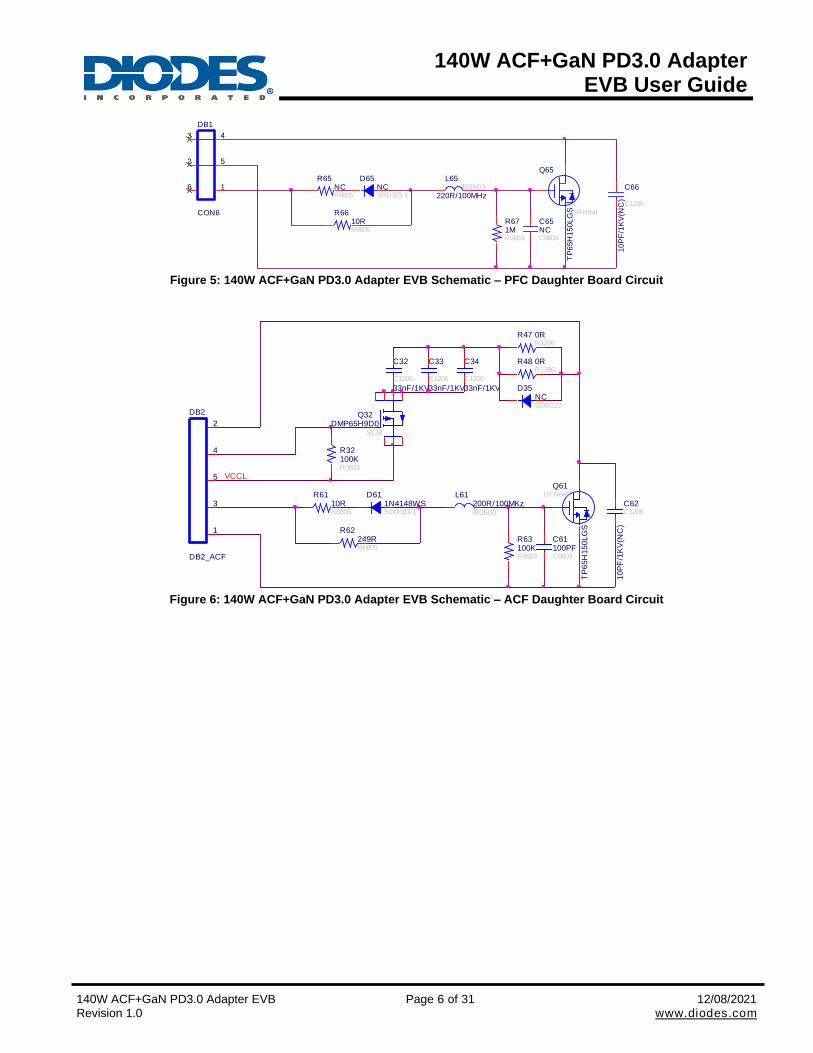
Figure 5: 140W ACF+GaN PD3.0 Adapter EVB Schematic – PFC Daughter Board Circuit
Figure 6: 140W ACF+GaN PD3.0 Adapter EVB Schematic – ACF Daughter Board Circuit
C66
10P
F/1
KV
(NC
)
C1206
Q65
TP
65H
150LG
SDFN8x8
D65NCSOD323-1
R671MR0603
R6610RR0805
DB1
CON6
1
2
3 4
5
6L65
220R/100MHzR0603
R65NCR0805
C65NCC0603
R48 0RR1206
C34
C1206
33nF/1KV
L61200R/100MKzR0603
DB2
DB2_ACF
1
2
3
4
5
Q32DMP65H9D0
SO8
D35NCSOD123
C32
33nF/1KV
C1206
R47 0RR1206
R6110RR0805
C61100PFC0603
C62
10P
F/1
KV
(NC
)
C1206
D611N4148WSSOD323-1
VCCL
R63100KR0603
R32100KR0603
C33
C1206
33nF/1KV
Q61
TP
65H
150LG
S
DFN8x8
R62249RR0805
140W ACF+GaN PD3.0 Adapter EVB User Guide
140W ACF+GaN PD3.0 Adapter EVB Page 7 of 31 12/08/2021 Revision 1.0 www.diodes.com
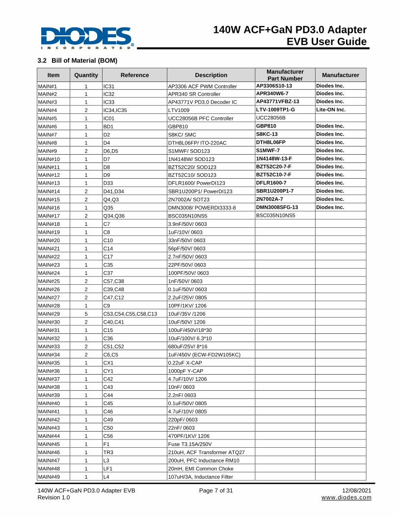
3.2 Bill of Material (BOM)
Item Quantity Reference Description Manufacturer Part Number
Manufacturer
MAIN#1 1 IC31 AP3306 ACF PWM Controller AP3306S10-13 Diodes Inc.
MAIN#2 1 IC32 APR340 SR Controller APR340W6-7 Diodes Inc.
MAIN#3 1 IC33 AP43771V PD3.0 Decoder IC AP43771VFBZ-13 Diodes Inc.
MAIN#4 2 IC34,IC35 LTV1009 LTV-1009TP1-G Lite-ON Inc.
MAIN#5 1 IC01 UCC28056B PFC Controller UCC28056B
MAIN#6 1 BD1 GBP810 GBP810 Diodes Inc.
MAIN#7 1 D2 S8KC/ SMC S8KC-13 Diodes Inc.
MAIN#8 1 D4 DTH8L06FP/ ITO-220AC DTH8L06FP Diodes Inc.
MAIN#9 2 D6,D5 S1MWF/ SOD123 S1MWF-7 Diodes Inc.
MAIN#10 1 D7 1N4148W/ SOD123 1N4148W-13-F Diodes Inc.
MAIN#11 1 D8 BZT52C20/ SOD123 BZT52C20-7-F Diodes Inc.
MAIN#12 1 D9 BZT52C10/ SOD123 BZT52C10-7-F Diodes Inc.
MAIN#13 1 D33 DFLR1600/ PowerDI123 DFLR1600-7 Diodes Inc.
MAIN#14 2 D41,D34 SBR1U200P1/ PowerDI123 SBR1U200P1-7 Diodes Inc.
MAIN#15 2 Q4,Q3 2N7002A/ SOT23 2N7002A-7 Diodes Inc.
MAIN#16 1 Q35 DMN3008/ POWERDI3333-8 DMN3008SFG-13 Diodes Inc.
MAIN#17 2 Q34,Q36 BSC035N10NS5 BSC035N10NS5
MAIN#18 1 C7 3.9nF/50V/ 0603
MAIN#19 1 C8 1uF/10V/ 0603
MAIN#20 1 C10 33nF/50V/ 0603
MAIN#21 1 C14 56pF/50V/ 0603
MAIN#22 1 C17 2.7nF/50V/ 0603
MAIN#23 1 C35 22PF/50V/ 0603
MAIN#24 1 C37 100PF/50V/ 0603
MAIN#25 2 C57,C38 1nF/50V/ 0603
MAIN#26 2 C39,C48 0.1uF/50V/ 0603
MAIN#27 2 C47,C12 2.2uF/25V/ 0805
MAIN#28 1 C9 10PF/1KV/ 1206
MAIN#29 5 C53,C54,C55,C58,C13 10uF/35V /1206
MAIN#30 2 C40,C41 10uF/50V/ 1206
MAIN#31 1 C15 100uF/450V/18*30
MAIN#32 1 C36 10uF/100V/ 6.3*10
MAIN#33 2 C51,C52 680uF/25V/ 8*16
MAIN#34 2 C6,C5 1uF/450V (ECW-FD2W105KC)
MAIN#35 1 CX1 0.22uF X-CAP
MAIN#36 1 CY1 1000pF Y-CAP
MAIN#37 1 C42 4.7uF/10V/ 1206
MAIN#38 1 C43 10nF/ 0603
MAIN#39 1 C44 2.2nF/ 0603
MAIN#40 1 C45 0.1uF/50V/ 0805
MAIN#41 1 C46 4.7uF/10V/ 0805
MAIN#42 1 C49 220pF/ 0603
MAIN#43 1 C50 22nF/ 0603
MAIN#44 1 C56 470PF/1KV/ 1206
MAIN#45 1 F1 Fuse T3.15A/250V
MAIN#46 1 TR3 210uH, ACF Transformer ATQ27
MAIN#47 1 L3 200uH, PFC Inductance RM10
MAIN#48 1 LF1 20mH, EMI Common Choke
MAIN#49 1 L4 107uH/3A, Inductance Filter
140W ACF+GaN PD3.0 Adapter EVB User Guide
140W ACF+GaN PD3.0 Adapter EVB Page 8 of 31 12/08/2021 Revision 1.0 www.diodes.com
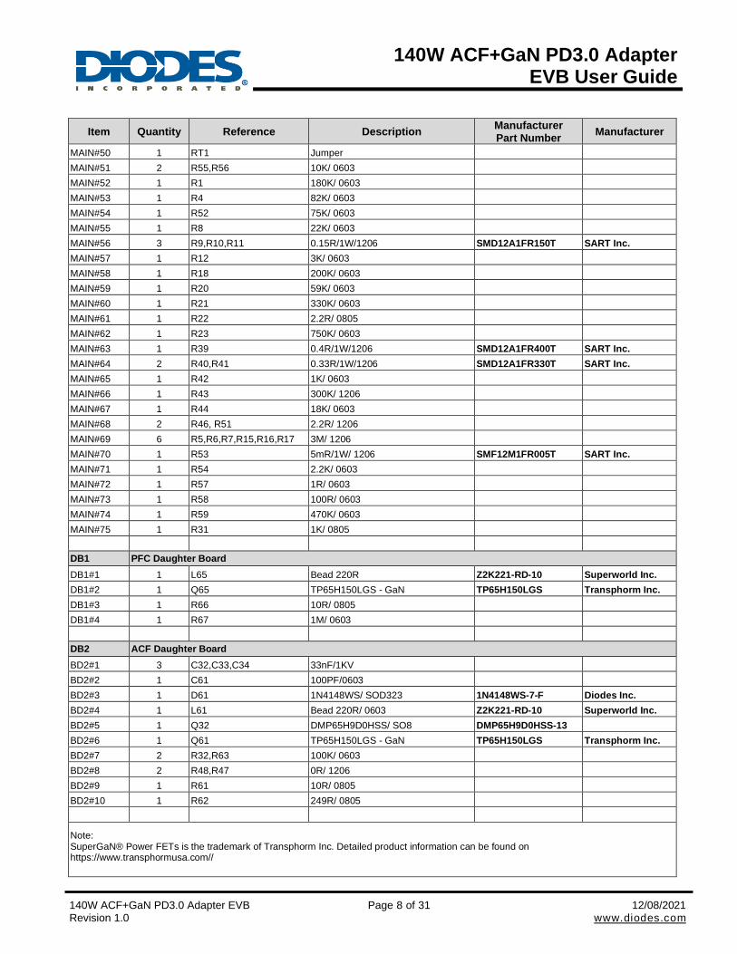
Item Quantity Reference Description Manufacturer Part Number
Manufacturer
MAIN#50 1 RT1 Jumper
MAIN#51 2 R55,R56 10K/ 0603
MAIN#52 1 R1 180K/ 0603
MAIN#53 1 R4 82K/ 0603
MAIN#54 1 R52 75K/ 0603
MAIN#55 1 R8 22K/ 0603
MAIN#56 3 R9,R10,R11 0.15R/1W/1206 SMD12A1FR150T SART Inc.
MAIN#57 1 R12 3K/ 0603
MAIN#58 1 R18 200K/ 0603
MAIN#59 1 R20 59K/ 0603
MAIN#60 1 R21 330K/ 0603
MAIN#61 1 R22 2.2R/ 0805
MAIN#62 1 R23 750K/ 0603
MAIN#63 1 R39 0.4R/1W/1206 SMD12A1FR400T SART Inc.
MAIN#64 2 R40,R41 0.33R/1W/1206 SMD12A1FR330T SART Inc.
MAIN#65 1 R42 1K/ 0603
MAIN#66 1 R43 300K/ 1206
MAIN#67 1 R44 18K/ 0603
MAIN#68 2 R46, R51 2.2R/ 1206
MAIN#69 6 R5,R6,R7,R15,R16,R17 3M/ 1206
MAIN#70 1 R53 5mR/1W/ 1206 SMF12M1FR005T SART Inc.
MAIN#71 1 R54 2.2K/ 0603
MAIN#72 1 R57 1R/ 0603
MAIN#73 1 R58 100R/ 0603
MAIN#74 1 R59 470K/ 0603
MAIN#75 1 R31 1K/ 0805
DB1 PFC Daughter Board
DB1#1 1 L65 Bead 220R Z2K221-RD-10 Superworld Inc.
DB1#2 1 Q65 TP65H150LGS - GaN TP65H150LGS Transphorm Inc.
DB1#3 1 R66 10R/ 0805
DB1#4 1 R67 1M/ 0603
DB2 ACF Daughter Board
BD2#1 3 C32,C33,C34 33nF/1KV
BD2#2 1 C61 100PF/0603
BD2#3 1 D61 1N4148WS/ SOD323 1N4148WS-7-F Diodes Inc.
BD2#4 1 L61 Bead 220R/ 0603 Z2K221-RD-10 Superworld Inc.
BD2#5 1 Q32 DMP65H9D0HSS/ SO8 DMP65H9D0HSS-13
BD2#6 1 Q61 TP65H150LGS - GaN TP65H150LGS Transphorm Inc.
BD2#7 2 R32,R63 100K/ 0603
BD2#8 2 R48,R47 0R/ 1206
BD2#9 1 R61 10R/ 0805
BD2#10 1 R62 249R/ 0805
Note: SuperGaN® Power FETs is the trademark of Transphorm Inc. Detailed product information can be found on https://www.transphormusa.com//

140W ACF+GaN PD3.0 Adapter EVB User Guide
140W ACF+GaN PD3.0 Adapter EVB Page 9 of 31 12/08/2021 Revision 1.0 www.diodes.com
3.3 PFC Inductance, Transformer Design
3.3.1 PFC Inductance
Circuit: Cross sectional view:
11,12
WD1
1, 2
WD1
BOBBIN
WD11T
OVER CORE3Ts
Definition Pin define
(Start >> End) Wire (φ) Turn (Ts) Layers Layers of Tape
WD1 11,12 >> 1,2 2UEW Litz Wire 0.1mm x 60P 36
OVER CORE 3Ts
Note:
1) L=200uH, RM10, Bobbin: BOJUN: BJ-RM-1002
2) Core plus cross capper foil for EMI shielding.
3) Picture and Pin define

140W ACF+GaN PD3.0 Adapter EVB User Guide
140W ACF+GaN PD3.0 Adapter EVB Page 10 of 31 12/08/2021 Revision 1.0 www.diodes.com
3.3.2 ACF Transformer
Circuit: Cross sectional view:
4
WD1
WD8
3WD2
Start
Teflon Tube
Primary Secondary
1
3
FL1
WD3a/3b
WD7
3
Black Teflon Tube
5
a
WD5
FL2
FL3
WD4
WD62
WD1
BOBBIN
WD11T
1T
2Ts
1T
1T
1T
2TsOVER CORE
WD2
WD5
WD4
WD3b
WD3a
WD6
WD7
WD8
3Ts
Definition Pin define
(Start >> End) Wire (φ) Turn (Ts) Layers Layers of Tape
WD1 4 >> a 2UEW-B Litz Wire 0.1mm*22 x1P 21 2 1T
WD2 3 >> Null 2UEW-B 0.2mm x 1P 20 1 1T
WD3a FL2 >> FL1 Triple Litz wire-B 0.22mm*7 x 2P 4 1
2Ts WD3b FL2 >> FL1 Triple Litz wire-B 0.22mm*7 x 2P 4 1
WD4 FL3 >> FL2 Triple wire-B 0.25mm x 1P 4 1
WD5 3 >> Null 2UEW-B 0.2mm x 1P 18 1 1T
WD6 1 >> 2 2UEW-B 0.2mm x 1P 5 1 1T
WD7 2 >> 3 2UEW-B 0.2mm x 1P 5
WD8 a >> 5 2UEW-B Litz Wire 0.1mm*22x1P 9 1 2Ts
OVER CORE (22mm) 3Ts
Note: a.> Core: ATQ27-16.6-1 GP95, Bobbin: XHW ATQ2716 (5+2)
b.> Lm=210uH

140W ACF+GaN PD3.0 Adapter EVB User Guide
140W ACF+GaN PD3.0 Adapter EVB Page 11 of 31 12/08/2021 Revision 1.0 www.diodes.com
3.4 Schematics Description
3.4.1 AC Input Circuit & Differential Filter
The Fuse F1 protects against over-current conditions which occur when some main components fails. The LF1 is common mode chocks for the common mode noise suppression. The BD is a bridge rectifier which converts alternating current and voltage into direct current and voltage. The C5, C6, L4 are composed of the Pi filter for filtering the differential switching noise back to AC source.
3.4.2 UCC28056 PFC Controller
The UCC28056 device drives PFC boost stages based on an innovative mixed mode method that operates in transition mode (TM) at full load and transitions seamlessly into discontinuous conduction mode (DCM) at reduced load, automatically reducing switching frequency. This device incorporates burst mode operation to further improve light load performance, enabling systems to meet challenging energy standards while eliminating the need to switch off the PFC.
3.4.3 AP3306 PWM Controller
AP3306, a highly integrated Active Clamp Flyback (ACF) controller, integrates high-voltage start-up function through HV pin and X-Cap discharging function. It also integrates a VCCL LDO circuit, which allows the LDO to regulate the wide range VCCL to an acceptable value. This makes AP3306 an ideal candidate for wide range output voltage applications such as USB-PD3.0. With embedded high-side and low-side switch control mechanism, AP3306 provides proper timing sequences to control Q32 (high-side Switch) and Q61 (low-side Switch) operations to implement two key efficiency improvement approaches, namely, ZVS (Zero Voltage Switching) and leakage energy recycling (stored in Csn1) to achieve high-power density charger applications. At no load or light load, the AP3306 will enter the burst mode to minimize standby power consumption.
3.4.4 APR340 Synchronous Rectification (SR) MOSFET Driver
As a high performance solution, APR340 is a secondary side SR controller to effectively reduce the secondary side rectifier power dissipation which works in DCM-QR/ACF operation.
3.4.5 AP43771V PD 3.0 Decoder & Protection on/off N MOSFET and Interface to Power Devices
Few important pins provide critical protocol decoding and regulation functions in AP43771V:
1) CC1 (Pin 11): CC1 is defined by USB Type-C spec to provide the channel communication link between power source
and sink device.
2) CC2 (Pin 10): To control PFC Converter turn on/off, “0” To disable PFC converter, “1” To enable PFC converter. When
PD request to 20V PDO, AP43771V_CC2 output “1” to turn on PFC Converter. It through Opto-coupler IC35 to control
VCC_PFC of PFC Converter to turn on/off.
3) Constant Voltage (CV): The CV is implemented by sensing VFB (pin 8) and comparing with internal reference voltage
to generate a CV compensation signal on the OCDRV pin (pin 5). The output voltage is controlled by firmware through
CC1 channel communication with the sink device.
4) Constant Current (CC): The CC is implemented by sensing the current sense resistor (RCS, 10mΩ, 1%, Low TCR)
and compared with internal programmable reference voltage. The output current is controlled by firmware through CC1
channel communication with the sink device.
5) Loop Compensation: R56, C48 & C49 form the voltage loop compensation circuit, and C50 form the current loop
compensation circuit.
6) OCDRV (Pin5): It is the key interface link from secondary decoder (AP43771V) to primary regulation circuit (AP3306).
It is connected to Opto-coupler IC34 Pin 2 (Cathode) for feedback information based on all sensed CC1 signals for
getting desired Vbus voltage & current.
7) PWR_EN (Pin2) to N-MOSFET Gate: The pin is used to turn on/off N-MOSFET (Q35) to enable/disable voltage output
to the Vbus.

140W ACF+GaN PD3.0 Adapter EVB User Guide
140W ACF+GaN PD3.0 Adapter EVB Page 12 of 31 12/08/2021 Revision 1.0 www.diodes.com
Chapter 4 The Evaluation Board (EVB) Connections
4.1 EVB PCB Layout
Figure 7: 140W ACF+GaN PD3.0 Adapter EVB Main Board PCB Layout – Top View
Figure 8: 140W ACF+GaN PD3.0 Adapter EVB Main Board PCB Layout – Bottom View

140W ACF+GaN PD3.0 Adapter EVB User Guide
140W ACF+GaN PD3.0 Adapter EVB Page 13 of 31 12/08/2021 Revision 1.0 www.diodes.com
Figure 9-1: DB1- PFC Daughter Board Drawing
Figure 9-2: DB1 Top View
Figure 9-3: DB1 Bottom View
Figure 9: 140W ACF+GaN PD3.0 Adapter EVB DB1 PCB Layout
Figure 10-1: DB2- ACF Daughter Board Drawing
Figure 10-2: DB2 Top View
Figure 10-3: DB2 Bottom View
Figure 10: 140W ACF+GaN PD3.0 Adapter EVB DB2 PCB Layout
140W ACF+GaN PD3.0 Adapter EVB User Guide
140W ACF+GaN PD3.0 Adapter EVB Page 14 of 31 12/08/2021 Revision 1.0 www.diodes.com
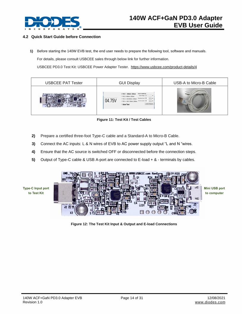
4.2 Quick Start Guide before Connection
1) Before starting the 140W EVB test, the end user needs to prepare the following tool, software and manuals.
For details, please consult USBCEE sales through below link for further information.
USBCEE PD3.0 Test Kit: USBCEE Power Adapter Tester. https://www.usbcee.com/product-details/4
USBCEE PAT Tester GUI Display USB-A to Micro-B Cable
Figure 11: Test Kit / Test Cables
2) Prepare a certified three-foot Type-C cable and a Standard-A to Micro-B Cable.
3) Connect the AC inputs: L & N wires of EVB to AC power supply output “L and N “wires.
4) Ensure that the AC source is switched OFF or disconnected before the connection steps.
5) Output of Type-C cable & USB A-port are connected to E-load + & - terminals by cables.
Figure 12: The Test Kit Input & Output and E-load Connections
Type-C Input port
to Test Kit
Mini USB port
to computer

140W ACF+GaN PD3.0 Adapter EVB User Guide
140W ACF+GaN PD3.0 Adapter EVB Page 15 of 31 12/08/2021 Revision 1.0 www.diodes.com
4.3 Connection with E-Load
Figure 13: Diagram of Connections in the Sample Board
140W ACF+GaN PD3.0 Adapter EVB User Guide
140W ACF+GaN PD3.0 Adapter EVB Page 16 of 31 12/08/2021 Revision 1.0 www.diodes.com
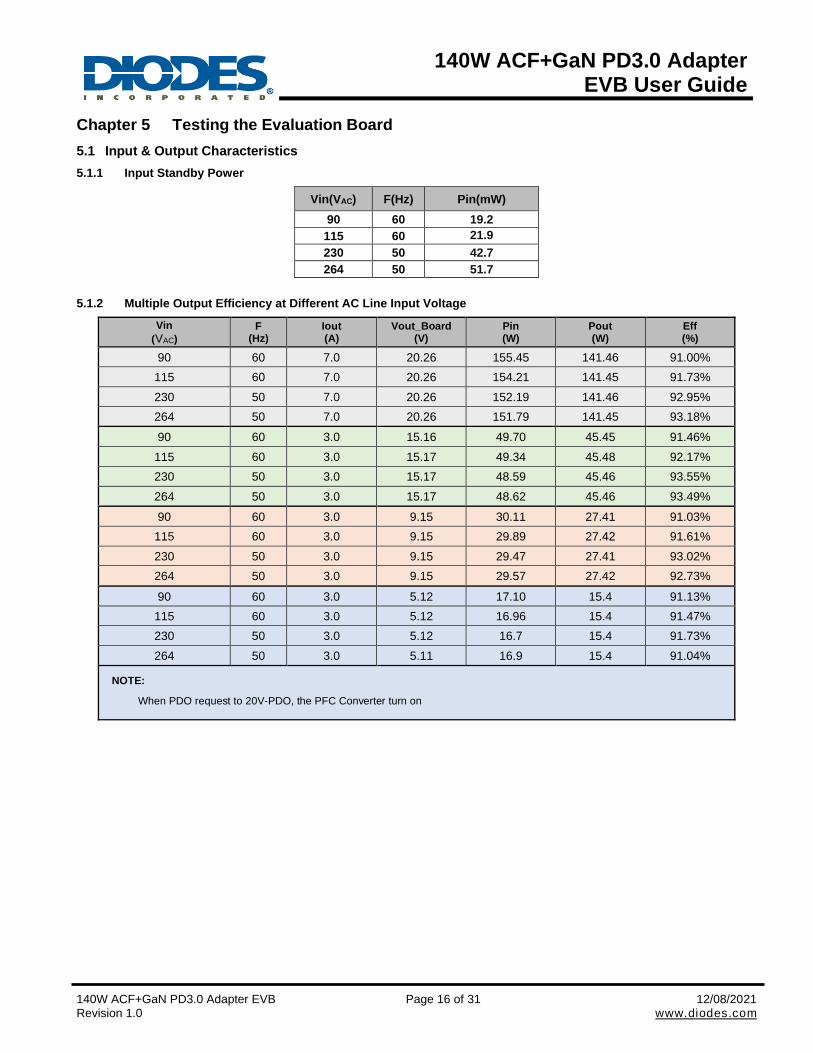
Chapter 5 Testing the Evaluation Board
5.1 Input & Output Characteristics
5.1.1 Input Standby Power
Vin(VAC) F(Hz) Pin(mW)
90 60 19.2
115 60 21.9
230 50 42.7
264 50 51.7
5.1.2 Multiple Output Efficiency at Different AC Line Input Voltage
Vin
(VAC)
F (Hz)
Iout (A)
Vout_Board (V)
Pin (W)
Pout (W)
Eff (%)
90 60 7.0 20.26 155.45 141.46 91.00%
115 60 7.0 20.26 154.21 141.45 91.73%
230 50 7.0 20.26 152.19 141.46 92.95%
264 50 7.0 20.26 151.79 141.45 93.18%
90 60 3.0 15.16 49.70 45.45 91.46%
115 60 3.0 15.17 49.34 45.48 92.17%
230 50 3.0 15.17 48.59 45.46 93.55%
264 50 3.0 15.17 48.62 45.46 93.49%
90 60 3.0 9.15 30.11 27.41 91.03%
115 60 3.0 9.15 29.89 27.42 91.61%
230 50 3.0 9.15 29.47 27.41 93.02%
264 50 3.0 9.15 29.57 27.42 92.73%
90 60 3.0 5.12 17.10 15.4 91.13%
115 60 3.0 5.12 16.96 15.4 91.47%
230 50 3.0 5.12 16.7 15.4 91.73%
264 50 3.0 5.11 16.9 15.4 91.04%
NOTE:
When PDO request to 20V-PDO, the PFC Converter turn on

140W ACF+GaN PD3.0 Adapter EVB User Guide
140W ACF+GaN PD3.0 Adapter EVB Page 17 of 31 12/08/2021 Revision 1.0 www.diodes.com
5.1.3 Efficiency vs. AC Line Input Voltage
Figure 14 illustrates the efficiency vs. input voltage
Figure 14: Efficiency vs. AC Line Input Voltage – PDO_5V/3A, 9V/3A, 15V/3A, and 20V/7A
85%
87%
89%
91%
93%
95%
90 120 150 180 210 240 270
EF
FIC
IEN
CY
(%)
INPUT VOLTAGE (VAC)
Efficiency vs. AC Line Input Voltage (Board End)
20V/7A 15V/3A
9V/3A 5V/3A

140W ACF+GaN PD3.0 Adapter EVB User Guide
140W ACF+GaN PD3.0 Adapter EVB Page 18 of 31 12/08/2021 Revision 1.0 www.diodes.com
5.1.4 Total Harmonic Distortion (THD) and Power Factor Correction (PFC)
Figure 15 illustrates the THD vs Output Power
Figure 15: THD vs. Output Power – Full Load 140W PDO_20V/7A
Figure 16 illustrates the Power Factor (PF) vs Output Power
Figure 16: PF vs. Output Power – Full Load 140W PDO_20V/7A
0
5
10
15
20
70 80 90 100 110 120 130 140
TH
D (
%)
Output Power (W)
THD vs Output Power
115VAC/ 60Hz
230VAC/ 50Hz
0.80
0.85
0.90
0.95
1.00
60 70 80 90 100 110 120 130 140
Po
wer
Facto
r
Output Power (W)
PF vs. Output Power
115VAC/ 60Hz
230VAC/ 50Hz

140W ACF+GaN PD3.0 Adapter EVB User Guide
140W ACF+GaN PD3.0 Adapter EVB Page 19 of 31 12/08/2021 Revision 1.0 www.diodes.com
5.1.5 Multiple Output Average Efficiency at Different Loading
PDO_20V / 15V / 9V / 5V Average Efficiency
PDO Mode Vin
(VAC)
F (Hz)
Remarks Iout (A)
Vout_Board (V)
Pin (W)
Pout_MB (W)
Eff (%)
Average Efficiency
20V/7A
115 60
100% 6.98 20.26 154.19 W 141.45 W 91.74%
91.38% 75% 5.25 20.25 115.74 W 106.22 W 91.77%
50% 3.49 20.23 77.25 W 70.61 W 91.41%
25% 1.74 20.21 38.74 W 35.09 W 90.59%
10% 0.69 20.20 15.74 W 13.88 W 88.20%
230 50
100% 6.98 20.26 152.24 W 141.43 W 92.90%
92.48% 75% 5.24 20.25 114.31 W 106.19 W 92.89%
50% 3.49 20.23 76.25 W 70.60 W 92.58%
25% 1.74 20.21 38.33 W 35.08 W 91.54%
10% 0.69 20.19 15.53 W 13.89 W 89.43%
15V/3A
115 60
100% 3.00 15.17 49.36 W 45.48 W 92.14%
92.11% 75% 2.25 15.16 36.95 W 34.06 W 92.18%
50% 1.50 15.14 24.57 W 22.66 W 92.24%
25% 0.75 15.12 12.29 W 11.30 W 91.91%
10% 0.30 15.11 5.02 W 4.48 W 89.20%
230 50
100% 3.00 15.17 48.57 W 45.46 W 93.59%
93.12% 75% 2.25 15.16 36.43 W 34.06 W 93.49%
50% 1.50 15.14 24.32 W 22.66 W 93.18%
25% 0.75 15.12 12.25 W 11.29 W 92.22%
10% 0.30 15.10 5.03 W 4.48 W 89.04%
9V/3A
115 60
100% 3.00 9.15 29.89 W 27.42 W 91.74%
91.81% 75% 2.25 9.12 22.31 W 20.50 W 91.88%
50% 1.50 9.09 14.81 W 13.62 W 91.94%
25% 0.75 9.06 7.39 W 6.78 W 91.69%
10% 0.30 9.04 3.02 W 2.68 W 88.70%
230 50
100% 3.00 9.15 29.47 W 27.41 W 93.02%
92.53% 75% 2.25 9.11 22.05 W 20.48 W 92.87%
50% 1.50 9.09 14.68 W 13.62 W 92.74%
25% 0.75 9.07 7.41 W 6.78 W 91.50%
10% 0.30 9.04 3.01 W 2.68 W 89.10%
5V/3A
115 60
100% 3.00 5.12 17.00 W 15.35 W 90.28%
89.75% 75% 2.25 5.09 12.68 W 11.44 W 90.26%
50% 1.50 5.05 8.44 W 7.58 W 89.83%
25% 0.75 5.02 4.25 W 3.77 W 88.61%
10% 0.30 5.00 1.72 W 1.49 W 86.69%
230 50
100% 3.00 5.12 16.87 W 15.34 W 90.96%
89.92% 75% 2.25 5.09 12.62 W 11.44 W 90.66%
50% 1.50 5.05 8.47 W 7.58 W 89.52%
25% 0.75 5.02 4.25 W 3.77 W 88.54%
10% 0.30 5.00 1.75 W 1.50 W 85.59%
140W ACF+GaN PD3.0 Adapter EVB User Guide
140W ACF+GaN PD3.0 Adapter EVB Page 20 of 31 12/08/2021 Revision 1.0 www.diodes.com
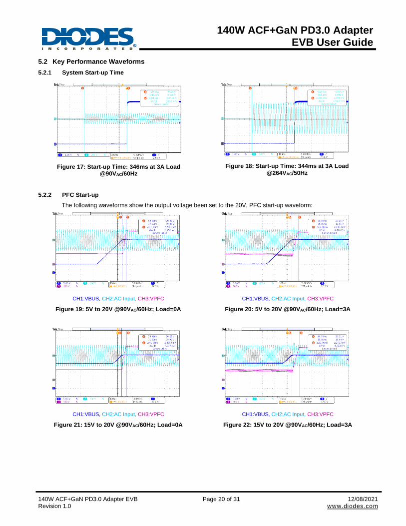
5.2 Key Performance Waveforms
5.2.1 System Start-up Time
Figure 17: Start-up Time: 346ms at 3A Load
@90VAC/60Hz
Figure 18: Start-up Time: 344ms at 3A Load
@264VAC/50Hz
5.2.2 PFC Start-up
The following waveforms show the output voltage been set to the 20V, PFC start-up waveform:
CH1:VBUS, CH2:AC Input, CH3:VPFC
Figure 19: 5V to 20V @90VAC/60Hz; Load=0A
CH1:VBUS, CH2:AC Input, CH3:VPFC
Figure 20: 5V to 20V @90VAC/60Hz; Load=3A
CH1:VBUS, CH2:AC Input, CH3:VPFC
Figure 21: 15V to 20V @90VAC/60Hz; Load=0A
CH1:VBUS, CH2:AC Input, CH3:VPFC
Figure 22: 15V to 20V @90VAC/60Hz; Load=3A

140W ACF+GaN PD3.0 Adapter EVB User Guide
140W ACF+GaN PD3.0 Adapter EVB Page 21 of 31 12/08/2021 Revision 1.0 www.diodes.com
5.2.3 Line Voltage and Line Current
CH2:AC Input, CH3:VPFC, CH4:AC Input Current
Figure 23: 20V/7A @90VAC/60Hz
CH2:AC Input, CH3:VPFC, CH4:AC Input Current
Figure 24: 20V/7A @115VAC/60Hz
CH2:AC Input, CH3:VPFC, CH4:AC Input Current
Figure 25: 20V/7A @230AC/50Hz
CH2:AC Input, CH3:VPFC, CH4:AC Input Current
Figure 26: 20V/7A @264VAC/50Hz

140W ACF+GaN PD3.0 Adapter EVB User Guide
140W ACF+GaN PD3.0 Adapter EVB Page 22 of 31 12/08/2021 Revision 1.0 www.diodes.com
5.2.4 Switching Transistor Voltage Stress
5.2.4.1 PFC Q65 GaN Vds Voltage stress
Figure 27: 20V/7A @90VAC/60Hz
Figure 28: 20V/7A @264VAC/50Hz
Component Input Voltage Output Vds Vds_Max_Spec Ratio of
voltage stress
Q65 90 VAC /60Hz
20V/7A 446V
650V 68.62%
264 VAC /50Hz 418V 64.31%
5.2.4.2 ACF Q61 GaN Vds Voltage stress
Figure 29: 20V/7A @90VAC/60Hz
Figure 30: 20V/7A @264VAC/50Hz
Component Input Voltage Output Vds Vds_Max_Spec Ratio of
voltage stress
Q61 90 VAC /60Hz
20V/7A 598V
650V 92%
264 VAC /50Hz 598V 92%
446Vmax 418Vmax
598Vmax 598Vmax

140W ACF+GaN PD3.0 Adapter EVB User Guide
140W ACF+GaN PD3.0 Adapter EVB Page 23 of 31 12/08/2021 Revision 1.0 www.diodes.com
5.2.4.3 ACF P-MOSFET Q32 Vds Voltage stress
Figure 31: 20V/7A @90VAC/60Hz
Figure 32: 20V/7A @264VAC/50Hz
Component Input Voltage Output Vds Vds_Max_Spec Ratio of
voltage stress
Q32 90 VAC /60Hz
20V/7A -562V
-600V 93.67%
264 VAC /50Hz -558V 93.00%
5.2.4.4 MOSFET Q34, Q36 Vds Voltage stress
Figure 33: 20V/7A @90VAC/60Hz
Figure 34: 20V/7A @264VAC/50Hz
Component Input Voltage Output Vds Vds_Max_Spec Ratio of
voltage stress
Q34, Q36 90 VAC /60Hz
20V/7A 82.4V
100V 82.40%
264 VAC /50Hz 79.2V 79.20%
-558Vmax -562Vmax
79.2Vmax 82.4Vmax
140W ACF+GaN PD3.0 Adapter EVB User Guide
140W ACF+GaN PD3.0 Adapter EVB Page 24 of 31 12/08/2021 Revision 1.0 www.diodes.com
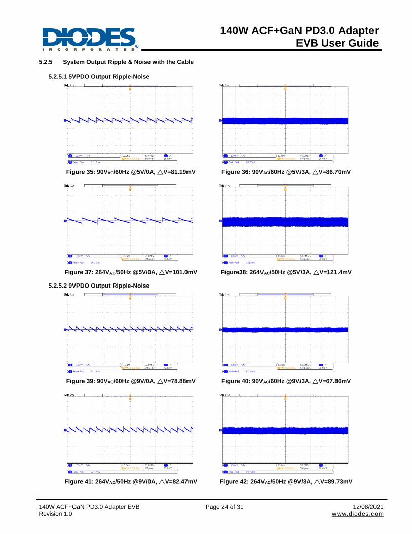
5.2.5 System Output Ripple & Noise with the Cable
5.2.5.1 5VPDO Output Ripple-Noise
Figure 35: 90VAC/60Hz @5V/0A, △V=81.19mV
Figure 36: 90VAC/60Hz @5V/3A, △V=86.70mV
Figure 37: 264VAC/50Hz @5V/0A, △V=101.0mV
Figure38: 264VAC/50Hz @5V/3A, △V=121.4mV
5.2.5.2 9VPDO Output Ripple-Noise
Figure 39: 90VAC/60Hz @9V/0A, △V=78.88mV
Figure 40: 90VAC/60Hz @9V/3A, △V=67.86mV
Figure 41: 264VAC/50Hz @9V/0A, △V=82.47mV
Figure 42: 264VAC/50Hz @9V/3A, △V=89.73mV

140W ACF+GaN PD3.0 Adapter EVB User Guide
140W ACF+GaN PD3.0 Adapter EVB Page 25 of 31 12/08/2021 Revision 1.0 www.diodes.com
5.2.5.3 15VPDO Output Ripple-Noise
Figure 43: 90VAC/60Hz @15V/0A, △V=55.00mV
Figure 44: 90VAC/60Hz @15V/3A, △V=60.52mV
Figure 45: 264VAC/50Hz @15V/0A, △V=76.16mV
Figure 46: 264VAC/50Hz @15V/3A, △V=80.23mV
5.2.5.4 20VPDO Output Ripple-Noise
Figure 47: 90VAC/60Hz @20V/0A, △V=73.2mV
Figure 48: 90VAC/60Hz @20V/7A, △V=115.9mV
Figure 49: 264VAC/50Hz @20V/0A, △V=70.09mV
Figure 50: 264VAC/50Hz @20V/7A, △V=112.1mV
Note Test condition: Connect 47uF AL Cap and 0.1uF MLCC to the cable output unit in parallel

140W ACF+GaN PD3.0 Adapter EVB User Guide
140W ACF+GaN PD3.0 Adapter EVB Page 26 of 31 12/08/2021 Revision 1.0 www.diodes.com
5.2.6 Dynamic load
10% Load~100% Load, T=20mS, Rate=5mA/us (PCB End)
5.2.6.1 5V Dynamic Load
Figure 51: 90VAC/60Hz Port-C@ Vout=5V
Figure 52: 264VAC/50Hz Port-C@ Vout=5V
Vo_ Undershoot(V) Vo_ Overshoot(V)
Vin=90VAC/60Hz @5V 4.867 5.241
Vin=264VAC/50Hz @5V 4.863 5.266
5.2.6.2 9V Dynamic Load
Figure 53: 90VAC/60Hz Port-C@ Vout=9V
Figure 54: 264VAC/50Hz Port-C@ Vout=9V
Vo_ Undershoot(V) Vo_ Overshoot(V)
Vin=90VAC/60Hz @9V 8.888 9.276
Vin=264VAC/50Hz @9V 8.887 9.324

140W ACF+GaN PD3.0 Adapter EVB User Guide
140W ACF+GaN PD3.0 Adapter EVB Page 27 of 31 12/08/2021 Revision 1.0 www.diodes.com
5.2.6.3 15V Dynamic Load
Figure 55: 90VAC/60Hz Port-C@ Vout=15V
Figure 56: 264VAC/50Hz Port-C@ Vout=15V
Vo_ Undershoot(V) Vo_ Overshoot(V)
Vin=90VAC/60Hz @15V 14.83 15.32
Vin=264VAC/50Hz @15V 14.81 15.34
5.2.6.4 20V Dynamic Load
Figure 57: 90VAC/60Hz Port-C@ Vout=20V
Figure 58: 264VAC/50Hz Port-C@ Vout=20V
Vo_ Undershoot(V) Vo_ Overshoot(V)
Vin=90VAC/60Hz @20V 19.74 20.43
Vin=264VAC/50Hz @20V 19.74 20.44

140W ACF+GaN PD3.0 Adapter EVB User Guide
140W ACF+GaN PD3.0 Adapter EVB Page 28 of 31 12/08/2021 Revision 1.0 www.diodes.com
5.2.7 Output Voltage Transition Time
Figure 59: 5V 9V Transition Time =70.8ms
Figure 60: 9V 5V Transition Time =74.4ms
Figure 61: 9V 15V Transition Time =93.6ms
Figure 62: 15V 9V Transition Time =96.4ms
Figure 63: 15V 20V Transition Time =84.0ms
Figure 64: 20V 15V Transition Time =78.0ms

140W ACF+GaN PD3.0 Adapter EVB User Guide
140W ACF+GaN PD3.0 Adapter EVB Page 29 of 31 12/08/2021 Revision 1.0 www.diodes.com
5.2.8 Thermal Testing
Test Condition : 20V/7A @90VAC/60Hz
Location BD1 L3 Q65 IC01 D3 TR3 IC31
Temperature (°C) 91.6 68.4 74.5 68.2 67.7 100.0 88.9
Location Q61 Q32 Q34 Q36 IC32 Q35 R35
Temperature (°C) 76.6 90.7 93.7 91.4 99.3 81.8 84.4
Note: The Q32 added thermal pad to improve the component thermal.
The Q34, Q36 and TR3 added thermal glue to improve thermal.
Component temperatures can be further optimized with various system design and thermal
management approaches by manufacturers.
Test Condition: Vin=90VAC @ 20V/7A Full load Open Frame.
Figure 65: DB1 Components side
• BD1: Bridge Rectifier
• Q65: PFC High Voltage GaN FET
• Q61: ACF Primary Side High Voltage GaN FET
• Q32: ACF Primary Side High Voltage P-MOS
• Q34/Q36: ACF Secondary Side Sync-Rectifier
• IC31: AP3306, ACF Controller
• IC32: APR340, Sync-Rectifier Controller
• IC01: Transition-Mode PFC Controller
• L3: PFC Inductance
• D3: PFC HYPER-FAST Rectifier Diode
• TR3: ACF Transformer
• Q35: PD Load Switch • R35: PD Current Sense Resistor
Figure 66: Top Components side
Figure 67: Bottom Surface Mount side

140W ACF+GaN PD3.0 Adapter EVB User Guide
140W ACF+GaN PD3.0 Adapter EVB Page 30 of 31 12/08/2021 Revision 1.0 www.diodes.com
5.3 EMI (Conduction) Testing
EMI can be further optimized with various system design approaches by manufacturers. 5.3.1 115VAC testing results
Output Condition : 20V/7A
Figure 68: 115VAC/60Hz L line
Figure 69: 115VAC/60Hz N line
5.3.2 230VAC testing results
Output Condition : 20V/7A
Figure 70: 230VAC/50Hz L line
Figure 71: 230VAC/50Hz N line
150 kHz 30 MHz
dBµV
dBµV
1 PK
MAXH
2 AV
MAXHTDS
6DB
RBW 9 kHz
MT 1 s
Att 10 dB
1 MHz 10 MHz
0
10
20
30
40
50
60
70
80
90
100
1
Marker 1 [T1 ]
45.48 dBµV
458.000000000 kHz
EN55022Q
EN55022A
Date: 11.NOV.2021 14:32:59
EDIT PEAK LIST (Final Measurement Results)
Trace1: EN55022Q
Trace2: EN55022A
Trace3: ---
TRACE FREQUENCY LEVEL dBµV DELTA LIMIT dB
1 Quasi Peak 154 kHz 56.20 -9.58
2 Average 154 kHz 45.16 -10.61
2 Average 170 kHz 42.93 -12.02
2 Average 25.174 MHz 42.52 -7.47
1 Quasi Peak 25.182 MHz 49.60 -10.39
1 Quasi Peak 25.378 MHz 50.86 -9.13
2 Average 25.838 MHz 41.87 -8.12
1 Quasi Peak 25.986 MHz 49.30 -10.69
1 Quasi Peak 26.662 MHz 50.22 -9.77
2 Average 29.85 MHz 41.58 -8.41
Date: 11.NOV.2021 14:32:50
150 kHz 30 MHz
dBµV
dBµV
1 PK
MAXH
2 AV
MAXHTDS
6DB
RBW 9 kHz
MT 1 s
Att 10 dB
1 MHz 10 MHz
0
10
20
30
40
50
60
70
80
90
100
1
Marker 1 [T1 ]
41.53 dBµV
458.000000000 kHz
EN55022Q
EN55022A
Date: 11.NOV.2021 14:28:28
EDIT PEAK LIST (Final Measurement Results)
Trace1: EN55022Q
Trace2: EN55022A
Trace3: ---
TRACE FREQUENCY LEVEL dBµV DELTA LIMIT dB
1 Quasi Peak 150 kHz 58.73 -7.26
2 Average 150 kHz 43.28 -12.71
1 Quasi Peak 158 kHz 56.63 -8.93
2 Average 158 kHz 41.81 -13.75
1 Quasi Peak 24.95 MHz 51.56 -8.43
2 Average 24.95 MHz 43.05 -6.94
2 Average 25.09 MHz 43.37 -6.62
2 Average 25.202 MHz 43.53 -6.46
1 Quasi Peak 25.434 MHz 51.11 -8.88
1 Quasi Peak 26.558 MHz 50.91 -9.08
Date: 11.NOV.2021 14:28:18
150 kHz 30 MHz
dBµV
dBµV
1 PK
MAXH
2 AV
MAXHTDS
6DB
RBW 9 kHz
MT 1 s
Att 10 dB
1 MHz 10 MHz
0
10
20
30
40
50
60
70
80
90
100
1
Marker 1 [T1 ]
42.99 dBµV
458.000000000 kHz
EN55022Q
EN55022A
Date: 11.NOV.2021 14:23:22
EDIT PEAK LIST (Final Measurement Results)
Trace1: EN55022Q
Trace2: EN55022A
Trace3: ---
TRACE FREQUENCY LEVEL dBµV DELTA LIMIT dB
2 Average 150 kHz 43.31 -12.68
2 Average 198 kHz 42.75 -10.93
1 Quasi Peak 218 kHz 51.62 -11.27
1 Quasi Peak 226 kHz 51.41 -11.17
1 Quasi Peak 234 kHz 51.03 -11.27
1 Quasi Peak 242 kHz 50.49 -11.53
1 Quasi Peak 302 kHz 51.79 -8.39
2 Average 302 kHz 42.44 -7.74
2 Average 24.862 MHz 39.69 -10.30
2 Average 29.666 MHz 39.70 -10.29
Date: 11.NOV.2021 14:23:04
150 kHz 30 MHz
dBµV
dBµV
1 PK
MAXH
2 AV
MAXHTDS
6DB
RBW 9 kHz
MT 1 s
Att 10 dB
1 MHz 10 MHz
0
10
20
30
40
50
60
70
80
90
100
1
Marker 1 [T1 ]
42.51 dBµV
454.000000000 kHz
EN55022Q
EN55022A
Date: 11.NOV.2021 14:25:09
EDIT PEAK LIST (Final Measurement Results)
Trace1: EN55022Q
Trace2: EN55022A
Trace3: ---
TRACE FREQUENCY LEVEL dBµV DELTA LIMIT dB
1 Quasi Peak 150 kHz 56.90 -9.09
2 Average 150 kHz 45.25 -10.74
2 Average 174 kHz 38.97 -15.79
2 Average 202 kHz 41.76 -11.76
1 Quasi Peak 206 kHz 51.35 -12.01
1 Quasi Peak 218 kHz 50.46 -12.43
1 Quasi Peak 226 kHz 49.88 -12.70
1 Quasi Peak 250 kHz 47.81 -13.94
2 Average 27.262 MHz 39.22 -10.77
2 Average 29.782 MHz 39.68 -10.31
Date: 11.NOV.2021 14:25:01

140W ACF+GaN PD3.0 Adapter EVB User Guide
140W ACF+GaN PD3.0 Adapter EVB Page 31 of 31 12/08/2021 Revision 1.0 www.diodes.com
IMPORTANT NOTICE DIODES INCORPORATED MAKES NO WARRANTY OF ANY KIND, EXPRESS OR IMPLIED, WITH REGARDS TO THIS DOCUMENT, INCLUDING, BUT NOT LIMITED TO, THE IMPLIED WARRANTIES OF MERCHANTABILITY AND FITNESS FOR A PARTICULAR PURPOSE (AND THEIR EQUIVALENTS UNDER THE LAWS OF ANY JURISDICTION). Diodes Incorporated and its subsidiaries reserve the right to make modifications, enhancements, improvements, corrections or other changes without further notice to this document and any product described herein. Diodes Incorporated does not assume any liability arising out of the application or use of this document or any product described herein; neither does Diodes Incorporated convey any license under its patent or trademark rights, nor the rights of others. Any Customer or user of this document or products described herein in such applications shall assume all risks of such use and will agree to hold Diodes Incorporated and all the companies whose products are represented on Diodes Incorporated website, harmless against all damages. Diodes Incorporated does not warrant or accept any liability whatsoever in respect of any products purchased through unauthorized sales channel. Should Customers purchase or use Diodes Incorporated products for any unintended or unauthorized application, Customers shall indemnify and hold Diodes Incorporated and its representatives harmless against all claims, damages, expenses, and attorney fees arising out of, directly or indirectly, any claim of personal injury or death associated with such unintended or unauthorized application. Products described herein may be covered by one or more United States, international or foreign patents pending. Product names and markings noted herein may also be covered by one or more United States, international or foreign trademarks. This document is written in English but may be translated into multiple languages for reference. Only the English version of this document is the final and determinative format released by Diodes Incorporated.
LIFE SUPPORT Diodes Incorporated products are specifically not authorized for use as critical components in life support devices or systems without the express written approval of the Chief Executive Officer of Diodes Incorporated. As used herein: A. Life support devices or systems are devices or systems which: 1. are intended to implant into the body, or
2. support or sustain life and whose failure to perform when properly used in accordance with instructions for use provided in the labeling can be reasonably expected to result in significant injury to the user.
B. A critical component is any component in a life support device or system whose failure to perform can be reasonably expected to cause the failure of the life support device or to affect its safety or effectiveness. Customers represent that they have all necessary expertise in the safety and regulatory ramifications of their life support devices or systems, and acknowledge and agree that they are solely responsible for all legal, regulatory and safety-related requirements concerning their products and any use of Diodes Incorporated products in such safety-critical, life support devices or systems, notwithstanding any devices- or systems-related information or support that may be provided by Diodes Incorporated. Further, Customers must fully indemnify Diodes Incorporated and its representatives against any damages arising out of the use of Diodes Incorporated products in such safety-critical, life support devices or systems. Copyright © 2017, Diodes Incorporated www.diodes.com