Evaluation of GaN HEMTs in H3TRB Reliability Testing - MDPI
14
Citation: Rodriguez, J.A.; Tsoi, T.; Graves, D.; Bayne, S.B. Evaluation of GaN HEMTs in H 3 TRB Reliability Testing. Electronics 2022, 11, 1532. https://doi.org/10.3390/ electronics11101532 Academic Editors: Ching-Ming Lai, Yitao Liu and Elias Stathatos Received: 18 March 2022 Accepted: 9 May 2022 Published: 11 May 2022 Publisher’s Note: MDPI stays neutral with regard to jurisdictional claims in published maps and institutional affil- iations. Copyright: © 2022 by the authors. Licensee MDPI, Basel, Switzerland. This article is an open access article distributed under the terms and conditions of the Creative Commons Attribution (CC BY) license (https:// creativecommons.org/licenses/by/ 4.0/). electronics Article Evaluation of GaN HEMTs in H 3 TRB Reliability Testing Jose A. Rodriguez * , Tsz Tsoi, David Graves and Stephen B. Bayne Center for Pulsed Power and Power Electronics, Department of Electrical and Computer Engineering, Texas Tech University, Lubbock, TX 79409, USA; [email protected] (T.T.); [email protected] (D.G.); [email protected] (S.B.B.) * Correspondence: [email protected] Abstract: Gallium Nitride (GaN) power devices can offer better switching performance and higher efficiency than Silicon Carbide (SiC) and Silicon (Si) devices in power electronics applications. GaN has extensively been incorporated in electric vehicle charging stations and power supplies, subjected to harsh environmental conditions. Many reliability studies evaluate GaN power devices through thermal stresses during current conduction or pulsing, with a few focusing on high blocking voltage and high humidity. This paper compares GaN-on-Si High-Electron-Mobility Transistors (HEMT) device characteristics under a High Humidity, High Temperature, Reverse Bias (H 3 TRB) Test. Twenty- one devices from three manufacturers were subjected to 85 ◦ C and 85% relative humidity while blocking 80% of their voltage rating. Devices from two manufacturers utilize a cascade configuration with a silicon metal-oxide-semiconductor field-effect transistor (MOSFET), while the devices from the third manufacturer are lateral p-GaN HEMTs. Through characterization, three sample devices have exhibited degraded blocking voltage capability. The results of the H 3 TRB test and potential causes of the failure mode are discussed. Keywords: power electronics; reliability; wide-bandgap 1. Introduction Gallium Nitride (GaN) High-Electron-Mobility Transistors (HEMT) have become favorable devices for power electronics applications due to their high bandgap, mobility, and critical field [1]. GaN devices have lower thermal conductivity than silicon (Si) devices but offer lower overall power dissipation and improved efficiency [2]. Compared to Silicon Carbide (SiC) power devices, commercially available GaN HEMTs have lower blocking voltage capability due to their lateral design. However, they have lower parasitic capacitance, making them suitable for high-frequency operation [3]. The lower blocking voltage for GaN HEMTs can be overcome using modular power converter designs by stacking several low voltage devices for high voltage operation with high efficiency [2]. These characteristics have allowed the development of high-power density and high- efficiency power electronics systems, resulting in GaN HEMTs being heavily integrated into power supplies and fast chargers for EV applications [4]. These applications require high-power density systems that limit the available cooling capacity and thus operate the GaN HEMT at high operating temperatures. Implementing GaN HEMTs in EV charging stations means operating in potentially humid environments. Thus there is great interest in evaluating the reliability of GaN power HEMTs under thermal stresses. Reliability testing of GaN HEMTs has primarily focused on thermal stresses. A known reliability issue with GaN HEMTs is its dynamic on-state resistance due to hot-carrier injection and trap buffers [5], resulting in higher conduction losses and reduced current conduction. This effect is temperature-dependent and can be suppressed by using a substrate with high thermal conductivity, such as a SiC substrate [6]. However, most GaN HEMTs for power electronics applications are grown on a Si substrate due to cost [4], so reliability tests have focused on thermal stresses induced by a current bias. Several Electronics 2022, 11, 1532. https://doi.org/10.3390/electronics11101532 https://www.mdpi.com/journal/electronics
-
Upload
khangminh22 -
Category
Documents
-
view
0 -
download
0
Transcript of Evaluation of GaN HEMTs in H3TRB Reliability Testing - MDPI
Citation: Rodriguez, J.A.; Tsoi, T.;
Graves, D.; Bayne, S.B. Evaluation of
GaN HEMTs in H3TRB Reliability
Testing. Electronics 2022, 11, 1532.
https://doi.org/10.3390/
electronics11101532
Academic Editors: Ching-Ming Lai,
Yitao Liu and Elias Stathatos
Received: 18 March 2022
Accepted: 9 May 2022
Published: 11 May 2022
Publisher’s Note: MDPI stays neutral
with regard to jurisdictional claims in
published maps and institutional affil-
iations.
Copyright: © 2022 by the authors.
Licensee MDPI, Basel, Switzerland.
This article is an open access article
distributed under the terms and
conditions of the Creative Commons
Attribution (CC BY) license (https://
creativecommons.org/licenses/by/
4.0/).
electronics
Article
Evaluation of GaN HEMTs in H3TRB Reliability TestingJose A. Rodriguez * , Tsz Tsoi, David Graves and Stephen B. Bayne
Center for Pulsed Power and Power Electronics, Department of Electrical and Computer Engineering,Texas Tech University, Lubbock, TX 79409, USA; [email protected] (T.T.); [email protected] (D.G.);[email protected] (S.B.B.)* Correspondence: [email protected]
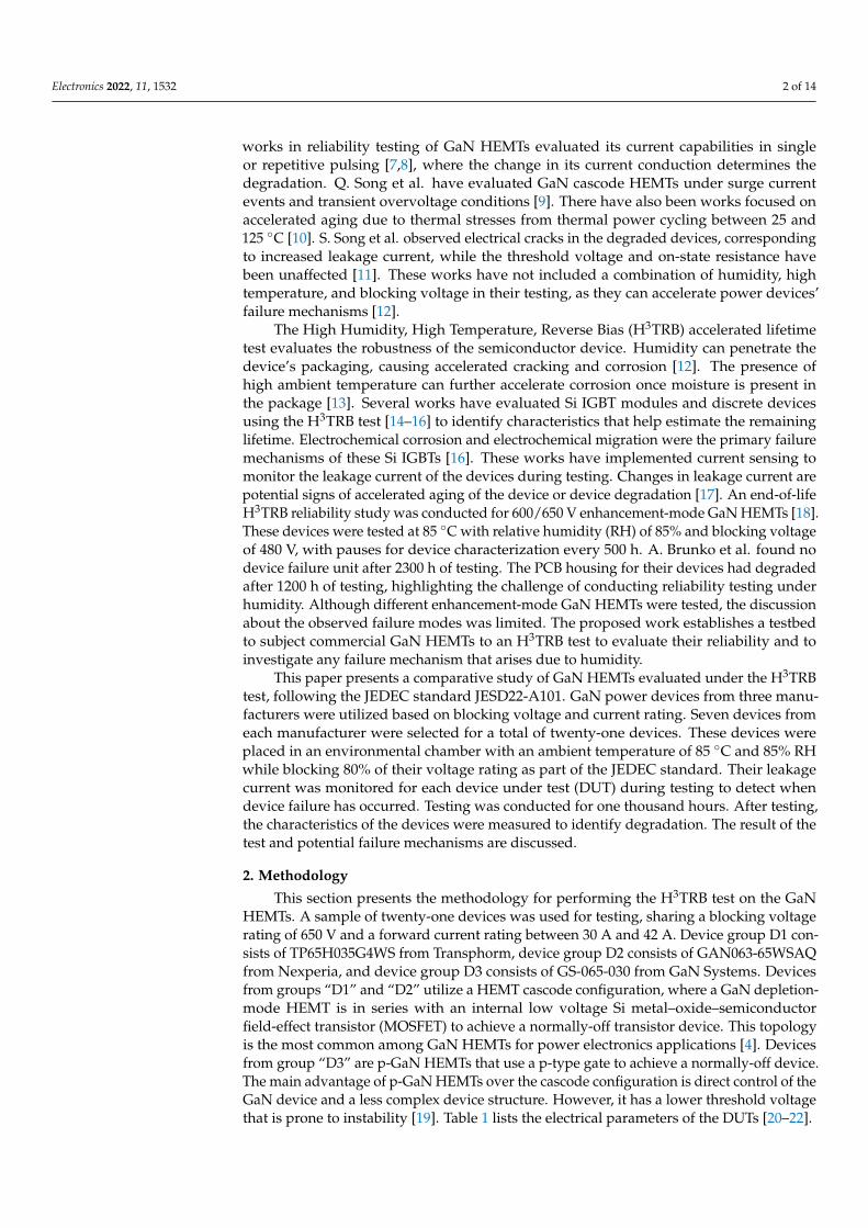
Abstract: Gallium Nitride (GaN) power devices can offer better switching performance and higherefficiency than Silicon Carbide (SiC) and Silicon (Si) devices in power electronics applications. GaNhas extensively been incorporated in electric vehicle charging stations and power supplies, subjectedto harsh environmental conditions. Many reliability studies evaluate GaN power devices throughthermal stresses during current conduction or pulsing, with a few focusing on high blocking voltageand high humidity. This paper compares GaN-on-Si High-Electron-Mobility Transistors (HEMT)device characteristics under a High Humidity, High Temperature, Reverse Bias (H3TRB) Test. Twenty-one devices from three manufacturers were subjected to 85 C and 85% relative humidity whileblocking 80% of their voltage rating. Devices from two manufacturers utilize a cascade configurationwith a silicon metal-oxide-semiconductor field-effect transistor (MOSFET), while the devices from thethird manufacturer are lateral p-GaN HEMTs. Through characterization, three sample devices haveexhibited degraded blocking voltage capability. The results of the H3TRB test and potential causes ofthe failure mode are discussed.
Keywords: power electronics; reliability; wide-bandgap
1. Introduction
Gallium Nitride (GaN) High-Electron-Mobility Transistors (HEMT) have becomefavorable devices for power electronics applications due to their high bandgap, mobility,and critical field [1]. GaN devices have lower thermal conductivity than silicon (Si) devicesbut offer lower overall power dissipation and improved efficiency [2]. Compared toSilicon Carbide (SiC) power devices, commercially available GaN HEMTs have lowerblocking voltage capability due to their lateral design. However, they have lower parasiticcapacitance, making them suitable for high-frequency operation [3]. The lower blockingvoltage for GaN HEMTs can be overcome using modular power converter designs bystacking several low voltage devices for high voltage operation with high efficiency [2].These characteristics have allowed the development of high-power density and high-efficiency power electronics systems, resulting in GaN HEMTs being heavily integratedinto power supplies and fast chargers for EV applications [4]. These applications requirehigh-power density systems that limit the available cooling capacity and thus operate theGaN HEMT at high operating temperatures. Implementing GaN HEMTs in EV chargingstations means operating in potentially humid environments. Thus there is great interest inevaluating the reliability of GaN power HEMTs under thermal stresses.
Reliability testing of GaN HEMTs has primarily focused on thermal stresses. A knownreliability issue with GaN HEMTs is its dynamic on-state resistance due to hot-carrierinjection and trap buffers [5], resulting in higher conduction losses and reduced currentconduction. This effect is temperature-dependent and can be suppressed by using asubstrate with high thermal conductivity, such as a SiC substrate [6]. However, most GaNHEMTs for power electronics applications are grown on a Si substrate due to cost [4],so reliability tests have focused on thermal stresses induced by a current bias. Several
Electronics 2022, 11, 1532. https://doi.org/10.3390/electronics11101532 https://www.mdpi.com/journal/electronics
Electronics 2022, 11, 1532 2 of 14
works in reliability testing of GaN HEMTs evaluated its current capabilities in singleor repetitive pulsing [7,8], where the change in its current conduction determines thedegradation. Q. Song et al. have evaluated GaN cascode HEMTs under surge currentevents and transient overvoltage conditions [9]. There have also been works focused onaccelerated aging due to thermal stresses from thermal power cycling between 25 and125 C [10]. S. Song et al. observed electrical cracks in the degraded devices, correspondingto increased leakage current, while the threshold voltage and on-state resistance havebeen unaffected [11]. These works have not included a combination of humidity, hightemperature, and blocking voltage in their testing, as they can accelerate power devices’failure mechanisms [12].
The High Humidity, High Temperature, Reverse Bias (H3TRB) accelerated lifetimetest evaluates the robustness of the semiconductor device. Humidity can penetrate thedevice’s packaging, causing accelerated cracking and corrosion [12]. The presence ofhigh ambient temperature can further accelerate corrosion once moisture is present inthe package [13]. Several works have evaluated Si IGBT modules and discrete devicesusing the H3TRB test [14–16] to identify characteristics that help estimate the remaininglifetime. Electrochemical corrosion and electrochemical migration were the primary failuremechanisms of these Si IGBTs [16]. These works have implemented current sensing tomonitor the leakage current of the devices during testing. Changes in leakage current arepotential signs of accelerated aging of the device or device degradation [17]. An end-of-lifeH3TRB reliability study was conducted for 600/650 V enhancement-mode GaN HEMTs [18].These devices were tested at 85 C with relative humidity (RH) of 85% and blocking voltageof 480 V, with pauses for device characterization every 500 h. A. Brunko et al. found nodevice failure unit after 2300 h of testing. The PCB housing for their devices had degradedafter 1200 h of testing, highlighting the challenge of conducting reliability testing underhumidity. Although different enhancement-mode GaN HEMTs were tested, the discussionabout the observed failure modes was limited. The proposed work establishes a testbedto subject commercial GaN HEMTs to an H3TRB test to evaluate their reliability and toinvestigate any failure mechanism that arises due to humidity.
This paper presents a comparative study of GaN HEMTs evaluated under the H3TRBtest, following the JEDEC standard JESD22-A101. GaN power devices from three manu-facturers were utilized based on blocking voltage and current rating. Seven devices fromeach manufacturer were selected for a total of twenty-one devices. These devices wereplaced in an environmental chamber with an ambient temperature of 85 C and 85% RHwhile blocking 80% of their voltage rating as part of the JEDEC standard. Their leakagecurrent was monitored for each device under test (DUT) during testing to detect whendevice failure has occurred. Testing was conducted for one thousand hours. After testing,the characteristics of the devices were measured to identify degradation. The result of thetest and potential failure mechanisms are discussed.
2. Methodology
This section presents the methodology for performing the H3TRB test on the GaNHEMTs. A sample of twenty-one devices was used for testing, sharing a blocking voltagerating of 650 V and a forward current rating between 30 A and 42 A. Device group D1 con-sists of TP65H035G4WS from Transphorm, device group D2 consists of GAN063-65WSAQfrom Nexperia, and device group D3 consists of GS-065-030 from GaN Systems. Devicesfrom groups “D1” and “D2” utilize a HEMT cascode configuration, where a GaN depletion-mode HEMT is in series with an internal low voltage Si metal–oxide–semiconductorfield-effect transistor (MOSFET) to achieve a normally-off transistor device. This topologyis the most common among GaN HEMTs for power electronics applications [4]. Devicesfrom group “D3” are p-GaN HEMTs that use a p-type gate to achieve a normally-off device.The main advantage of p-GaN HEMTs over the cascode configuration is direct control of theGaN device and a less complex device structure. However, it has a lower threshold voltagethat is prone to instability [19]. Table 1 lists the electrical parameters of the DUTs [20–22].
Electronics 2022, 11, 1532 3 of 14
Table 1. Characteristics of devices under test.
Device Parameter Group “D1” Group “D2” Group “D3” Unit
Part # TP65H035WS GAN063-650WSA GS-065-030-2-LBlocking Voltage 650 650 650 VForward Current 46.5 34.5 30 A
On-state Resistance 35 50 50 mΩThreshold Voltage 4 3.9 1.7 V
Forward Current @ Vth 1 1 10 mA
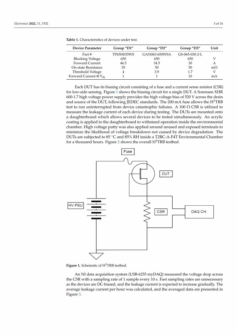
Each DUT has its biasing circuit consisting of a fuse and a current sense resistor (CSR)for low-side sensing. Figure 1 shows the biasing circuit for a single DUT. A Sorensen XHR600-1.7 high voltage power supply provides the high voltage bias of 520 V across the drainand source of the DUT, following JEDEC standards. The 200 mA fuse allows the H3TRBtest to run uninterrupted from device catastrophic failures. A 100 Ω CSR is utilized tomeasure the leakage current of each device during testing. The DUTs are mounted ontoa daughterboard which allows several devices to be tested simultaneously. An acryliccoating is applied to the daughterboard to withstand operation inside the environmentalchamber. High voltage putty was also applied around unused and exposed terminals tominimize the likelihood of voltage breakdown not caused by device degradation. TheDUTs are subjected to 85 C and 85% RH inside a T2RC-A-F4T Environmental Chamberfor a thousand hours. Figure 2 shows the overall H3TRB testbed.
Electronics 2022, 11, x FOR PEER REVIEW 3 of 15
threshold voltage that is prone to instability [19]. Table 1 lists the electrical parameters of the DUTs [20–22].
Table 1. Characteristics of devices under test.
Device Parameter Group “D1” Group “D2” Group “D3” Unit Part # TP65H035WS GAN063-650WSA GS-065-030-2-L
Blocking Voltage 650 650 650 V Forward Current 46.5 34.5 30 A
On-state Resistance 35 50 50 mΩ Threshold Voltage 4 3.9 1.7 V
Forward Current @ Vth 1 1 10 mA
Each DUT has its biasing circuit consisting of a fuse and a current sense resistor (CSR) for low-side sensing. Figure 1 shows the biasing circuit for a single DUT. A Sorensen XHR 600-1.7 high voltage power supply provides the high voltage bias of 520 V across the drain and source of the DUT, following JEDEC standards. The 200 mA fuse allows the H3TRB test to run uninterrupted from device catastrophic failures. A 100 Ω CSR is utilized to measure the leakage current of each device during testing. The DUTs are mounted onto a daughterboard which allows several devices to be tested simultaneously. An acrylic coat-ing is applied to the daughterboard to withstand operation inside the environmental chamber. High voltage putty was also applied around unused and exposed terminals to minimize the likelihood of voltage breakdown not caused by device degradation. The DUTs are subjected to 85 °C and 85% RH inside a T2RC-A-F4T Environmental Chamber for a thousand hours. Figure 2 shows the overall H3TRB testbed.
Figure 1. Schematic of H3TRB testbed.
Figure 1. Schematic of H3TRB testbed.
An NI data acquisition system (USB-6255 myDAQ) measured the voltage drop acrossthe CSR with a sampling rate of 1 sample every 10 s. Fast sampling rates are unnecessaryas the devices are DC-biased, and the leakage current is expected to increase gradually. Theaverage leakage current per hour was calculated, and the averaged data are presented inFigure 3.

Electronics 2022, 11, 1532 4 of 14Electronics 2022, 11, x FOR PEER REVIEW 4 of 15
Figure 2. H3TRB testbed.
An NI data acquisition system (USB-6255 myDAQ) measured the voltage drop across the CSR with a sampling rate of 1 sample every 10 s. Fast sampling rates are unnecessary as the devices are DC-biased, and the leakage current is expected to increase gradually. The average leakage current per hour was calculated, and the averaged data are presented in Figure 3.
Figure 3. Leakage current of DUT during testing.
The average leakage current for all devices was between 10 µA and 20 µA. Devices “D11”, “D13”, and “D17” exhibit an increase in leakage current before sharply increasing above the leakage current threshold of 200 µA. Table 2 shows a summary of the results from the H3TRB test. The fuses for these three DUTs were blown, suggesting that the de-vices had shorted during testing. From Figure 3, device “D11” is expected to have shorted 825 h into the test, device “D13” has shorted after 950 h, and device “D17” has shorted after 650 h. Device “D14” has also shown increased leakage current but has not sharply risen above the threshold like the other three devices. Leakage current data are missing
Figure 2. H3TRB testbed.
Electronics 2022, 11, x FOR PEER REVIEW 4 of 15
Figure 2. H3TRB testbed.
An NI data acquisition system (USB-6255 myDAQ) measured the voltage drop across the CSR with a sampling rate of 1 sample every 10 s. Fast sampling rates are unnecessary as the devices are DC-biased, and the leakage current is expected to increase gradually. The average leakage current per hour was calculated, and the averaged data are presented in Figure 3.
Figure 3. Leakage current of DUT during testing.
The average leakage current for all devices was between 10 µA and 20 µA. Devices “D11”, “D13”, and “D17” exhibit an increase in leakage current before sharply increasing above the leakage current threshold of 200 µA. Table 2 shows a summary of the results from the H3TRB test. The fuses for these three DUTs were blown, suggesting that the de-vices had shorted during testing. From Figure 3, device “D11” is expected to have shorted 825 h into the test, device “D13” has shorted after 950 h, and device “D17” has shorted after 650 h. Device “D14” has also shown increased leakage current but has not sharply risen above the threshold like the other three devices. Leakage current data are missing
Figure 3. Leakage current of DUT during testing.
The average leakage current for all devices was between 10 µA and 20 µA. Devices“D11”, “D13”, and “D17” exhibit an increase in leakage current before sharply increasingabove the leakage current threshold of 200 µA. Table 2 shows a summary of the results fromthe H3TRB test. The fuses for these three DUTs were blown, suggesting that the deviceshad shorted during testing. From Figure 3, device “D11” is expected to have shorted 825 hinto the test, device “D13” has shorted after 950 h, and device “D17” has shorted after 650 h.Device “D14” has also shown increased leakage current but has not sharply risen abovethe threshold like the other three devices. Leakage current data are missing for devices“D36” and “D37” due to a software error but were otherwise tested under the same testconditions as the other devices. Out of the sample of devices tested, devices “D11”, “D13”,and “D17” are considered degraded.
Electronics 2022, 11, 1532 5 of 14
Table 2. Summary of H3TRB test.
Device Group Failure Present Affected Devices Issue
D1 Yes D11, D13, D17 Opened fuseD2 No None NoneD3 No None None
3. Results
The characterization results of the DUTs are presented. The DUTs were characterizedusing a B1505A curve tracer before and after the test to identify degraded electrical char-acteristics. The blocking voltage curve, transfer characteristic curve, gate-source leakagecurve, and output characteristic curve was measured for all DUTs.
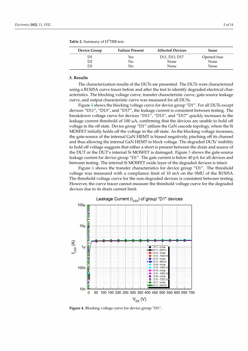
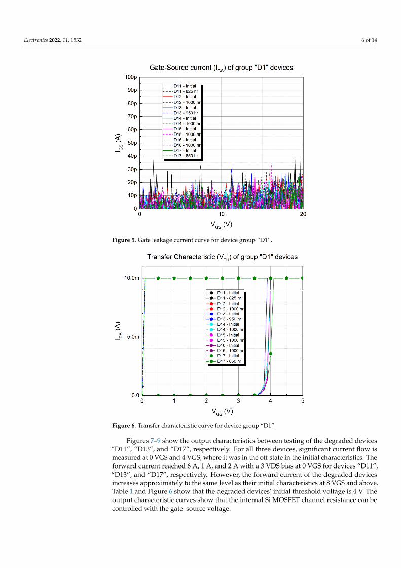
Figure 4 shows the blocking voltage curve for device group “D1”. For all DUTs exceptdevices “D11”, “D13”, and “D17”, the leakage current is consistent between testing. Thebreakdown voltage curve for devices “D11”, “D13”, and “D17” quickly increases to theleakage current threshold of 100 µA, confirming that the devices are unable to hold offvoltage in the off state. Device group “D1” utilizes the GaN cascode topology, where the SiMOSFET initially holds off the voltage in the off state. As the blocking voltage increases,the gate-source of the internal GaN HEMT is biased negatively, pinching off its channeland thus allowing the internal GaN HEMT to block voltage. The degraded DUTs’ inabilityto hold off voltage suggests that either a short is present between the drain and source ofthe DUT or the DUT’s internal Si MOSFET is damaged. Figure 5 shows the gate-sourceleakage current for device group “D1”. The gate current is below 40 pA for all devices andbetween testing. The internal Si MOSFET oxide layer of the degraded devices is intact.
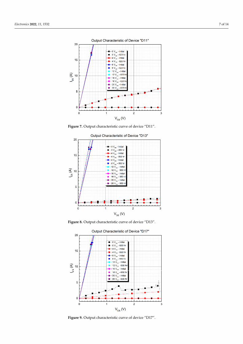
Figure 6 shows the transfer characteristics for device group “D1”. The thresholdvoltage was measured with a compliance limit of 10 mA on the SMU of the B1505A.The threshold voltage curve for the non-degraded devices is consistent between testing.However, the curve tracer cannot measure the threshold voltage curve for the degradeddevices due to its drain current limit.
Electronics 2022, 11, x FOR PEER REVIEW 5 of 15
for devices “D36” and “D37” due to a software error but were otherwise tested under the same test conditions as the other devices. Out of the sample of devices tested, devices “D11”, “D13”, and “D17” are considered degraded.
Table 2. Summary of H3TRB test.
Device Group Failure Present Affected Devices Issue D1 Yes D11, D13, D17 Opened fuse D2 No None None D3 No None None
3. Results The characterization results of the DUTs are presented. The DUTs were characterized
using a B1505A curve tracer before and after the test to identify degraded electrical char-acteristics. The blocking voltage curve, transfer characteristic curve, gate-source leakage curve, and output characteristic curve was measured for all DUTs.
Figure 4 shows the blocking voltage curve for device group “D1”. For all DUTs ex-cept devices “D11”, “D13”, and “D17”, the leakage current is consistent between testing. The breakdown voltage curve for devices “D11”, “D13”, and “D17” quickly increases to the leakage current threshold of 100 µA, confirming that the devices are unable to hold off voltage in the off state. Device group “D1” utilizes the GaN cascode topology, where the Si MOSFET initially holds off the voltage in the off state. As the blocking voltage in-creases, the gate-source of the internal GaN HEMT is biased negatively, pinching off its channel and thus allowing the internal GaN HEMT to block voltage. The degraded DUTs’ inability to hold off voltage suggests that either a short is present between the drain and source of the DUT or the DUT’s internal Si MOSFET is damaged. Figure 5 shows the gate-source leakage current for device group “D1”. The gate current is below 40 pA for all devices and between testing. The internal Si MOSFET oxide layer of the degraded devices is intact.
Figure 4. Blocking voltage curve for device group “D1”.
Figure 4. Blocking voltage curve for device group “D1”.
Electronics 2022, 11, 1532 6 of 14
Electronics 2022, 11, x FOR PEER REVIEW 6 of 15
Figure 5. Gate leakage current curve for device group “D1”.
Figure 6 shows the transfer characteristics for device group “D1”. The threshold volt-age was measured with a compliance limit of 10 mA on the SMU of the B1505A. The threshold voltage curve for the non-degraded devices is consistent between testing. How-ever, the curve tracer cannot measure the threshold voltage curve for the degraded de-vices due to its drain current limit.
Figure 6. Transfer characteristic curve for device group “D1”.
Figures 7–9 show the output characteristics between testing of the degraded devices “D11”, “D13”, and “D17”, respectively. For all three devices, significant current flow is measured at 0 VGS and 4 VGS, where it was in the off state in the initial characteristics. The forward current reached 6 A, 1 A, and 2 A with a 3 VDS bias at 0 VGS for devices “D11”, “D13”, and “D17”, respectively. However, the forward current of the degraded devices increases approximately to the same level as their initial characteristics at 8 VGS and above. Table 1 and Figure 6 show that the degraded devices’ initial threshold voltage
Figure 5. Gate leakage current curve for device group “D1”.
Electronics 2022, 11, x FOR PEER REVIEW 6 of 15
Figure 5. Gate leakage current curve for device group “D1”.
Figure 6 shows the transfer characteristics for device group “D1”. The threshold volt-age was measured with a compliance limit of 10 mA on the SMU of the B1505A. The threshold voltage curve for the non-degraded devices is consistent between testing. How-ever, the curve tracer cannot measure the threshold voltage curve for the degraded de-vices due to its drain current limit.
Figure 6. Transfer characteristic curve for device group “D1”.
Figures 7–9 show the output characteristics between testing of the degraded devices “D11”, “D13”, and “D17”, respectively. For all three devices, significant current flow is measured at 0 VGS and 4 VGS, where it was in the off state in the initial characteristics. The forward current reached 6 A, 1 A, and 2 A with a 3 VDS bias at 0 VGS for devices “D11”, “D13”, and “D17”, respectively. However, the forward current of the degraded devices increases approximately to the same level as their initial characteristics at 8 VGS and above. Table 1 and Figure 6 show that the degraded devices’ initial threshold voltage
Figure 6. Transfer characteristic curve for device group “D1”.
Figures 7–9 show the output characteristics between testing of the degraded devices“D11”, “D13”, and “D17”, respectively. For all three devices, significant current flow ismeasured at 0 VGS and 4 VGS, where it was in the off state in the initial characteristics. Theforward current reached 6 A, 1 A, and 2 A with a 3 VDS bias at 0 VGS for devices “D11”,“D13”, and “D17”, respectively. However, the forward current of the degraded devicesincreases approximately to the same level as their initial characteristics at 8 VGS and above.Table 1 and Figure 6 show that the degraded devices’ initial threshold voltage is 4 V. Theoutput characteristic curves show that the internal Si MOSFET channel resistance can becontrolled with the gate–source voltage.
Electronics 2022, 11, 1532 7 of 14
Electronics 2022, 11, x FOR PEER REVIEW 7 of 15
is 4 V. The output characteristic curves show that the internal Si MOSFET channel re-sistance can be controlled with the gate–source voltage.
Figure 7. Output characteristic curve of device “D11”.
Figure 8. Output characteristic curve of device “D13”.
Figure 7. Output characteristic curve of device “D11”.
Electronics 2022, 11, x FOR PEER REVIEW 7 of 15
is 4 V. The output characteristic curves show that the internal Si MOSFET channel re-sistance can be controlled with the gate–source voltage.
Figure 7. Output characteristic curve of device “D11”.
Figure 8. Output characteristic curve of device “D13”.
Figure 8. Output characteristic curve of device “D13”.
Electronics 2022, 11, x FOR PEER REVIEW 8 of 15
Figure 9. Output characteristic curve of device “D17”.
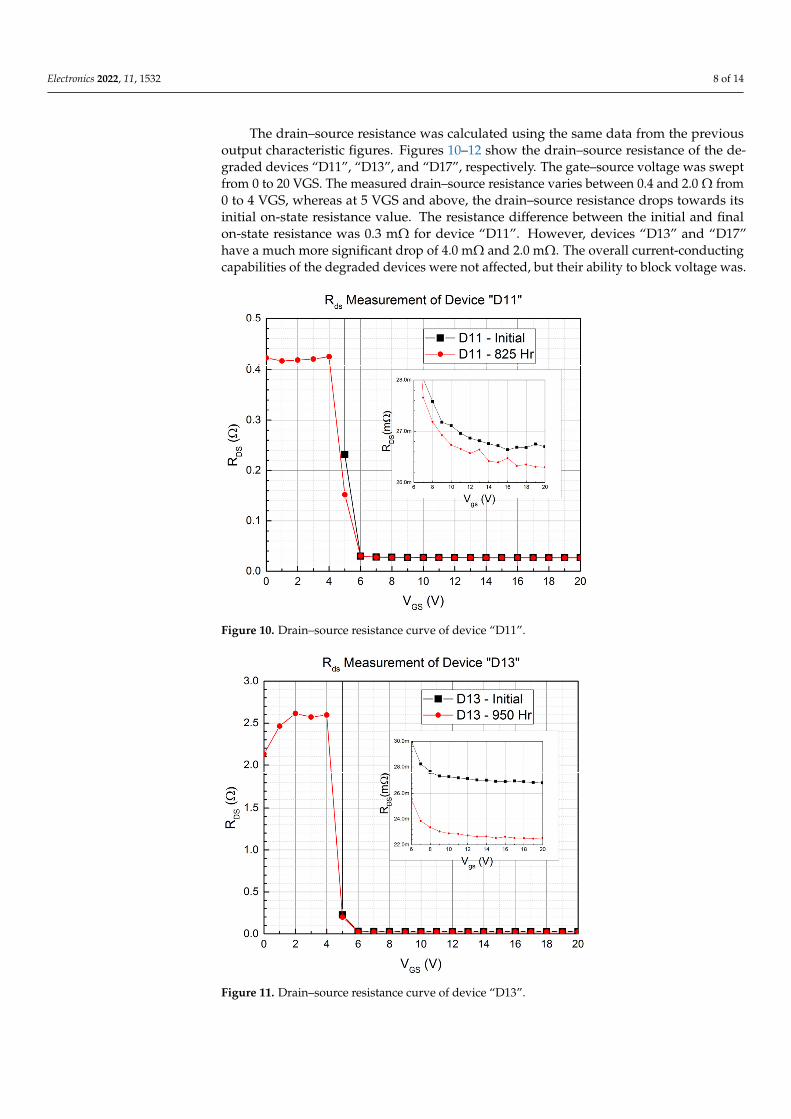
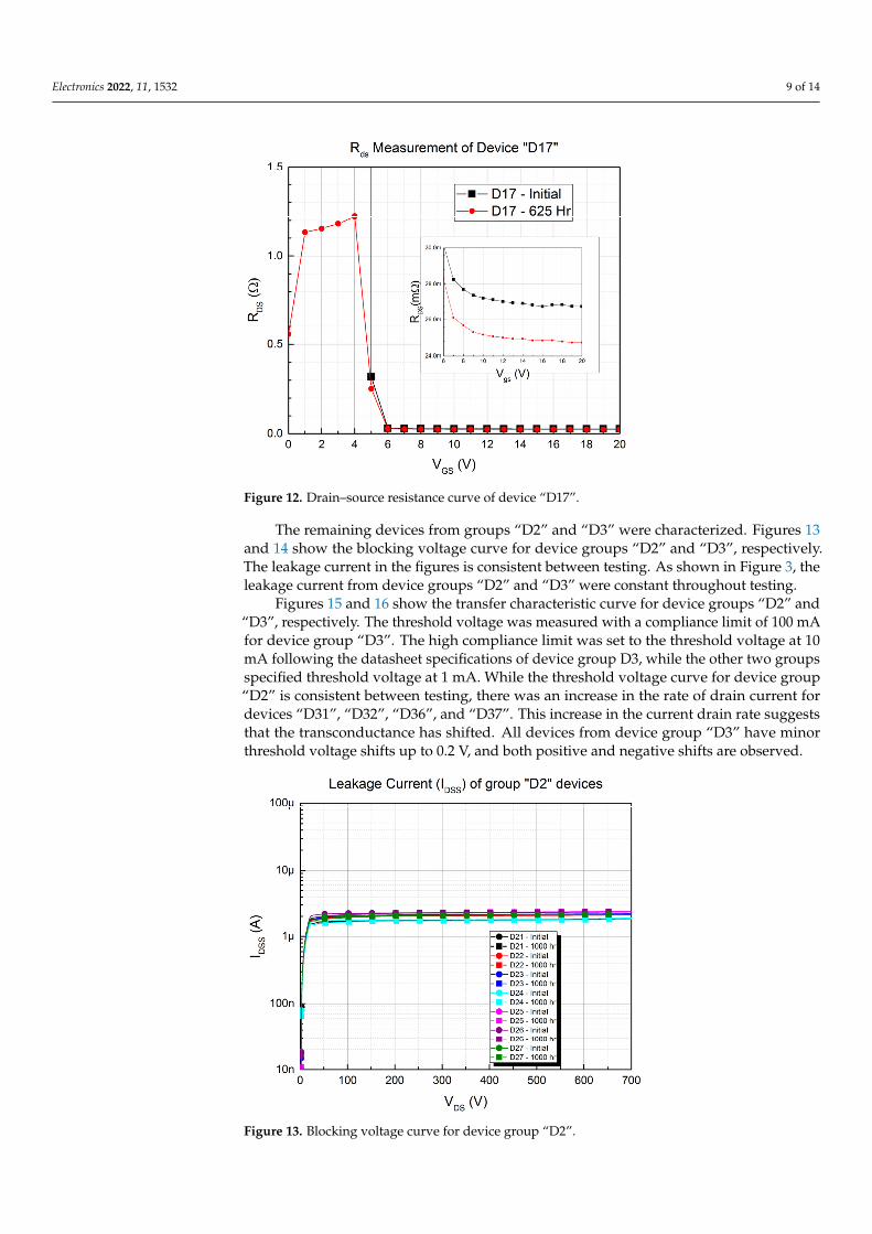
The drain–source resistance was calculated using the same data from the previous output characteristic figures. Figures 10–12 show the drain–source resistance of the de-graded devices “D11”, “D13”, and “D17”, respectively. The gate–source voltage was swept from 0 to 20 VGS. The measured drain–source resistance varies between 0.4 and 2.0 Ω from 0 to 4 VGS, whereas at 5 VGS and above, the drain–source resistance drops to-wards its initial on-state resistance value. The resistance difference between the initial and final on-state resistance was 0.3 mΩ for device “D11”. However, devices “D13” and “D17” have a much more significant drop of 4.0 mΩ and 2.0 mΩ. The overall current-conducting capabilities of the degraded devices were not affected, but their ability to block voltage was.
Figure 10. Drain–source resistance curve of device “D11”.
Figure 9. Output characteristic curve of device “D17”.
Electronics 2022, 11, 1532 8 of 14
The drain–source resistance was calculated using the same data from the previousoutput characteristic figures. Figures 10–12 show the drain–source resistance of the de-graded devices “D11”, “D13”, and “D17”, respectively. The gate–source voltage was sweptfrom 0 to 20 VGS. The measured drain–source resistance varies between 0.4 and 2.0 Ω from0 to 4 VGS, whereas at 5 VGS and above, the drain–source resistance drops towards itsinitial on-state resistance value. The resistance difference between the initial and finalon-state resistance was 0.3 mΩ for device “D11”. However, devices “D13” and “D17”have a much more significant drop of 4.0 mΩ and 2.0 mΩ. The overall current-conductingcapabilities of the degraded devices were not affected, but their ability to block voltage was.
Electronics 2022, 11, x FOR PEER REVIEW 8 of 15
Figure 9. Output characteristic curve of device “D17”.
The drain–source resistance was calculated using the same data from the previous output characteristic figures. Figures 10–12 show the drain–source resistance of the de-graded devices “D11”, “D13”, and “D17”, respectively. The gate–source voltage was swept from 0 to 20 VGS. The measured drain–source resistance varies between 0.4 and 2.0 Ω from 0 to 4 VGS, whereas at 5 VGS and above, the drain–source resistance drops to-wards its initial on-state resistance value. The resistance difference between the initial and final on-state resistance was 0.3 mΩ for device “D11”. However, devices “D13” and “D17” have a much more significant drop of 4.0 mΩ and 2.0 mΩ. The overall current-conducting capabilities of the degraded devices were not affected, but their ability to block voltage was.
Figure 10. Drain–source resistance curve of device “D11”.
Figure 10. Drain–source resistance curve of device “D11”.
Electronics 2022, 11, x FOR PEER REVIEW 9 of 15
Figure 11. Drain–source resistance curve of device “D13”.
Figure 12. Drain–source resistance curve of device “D17”.
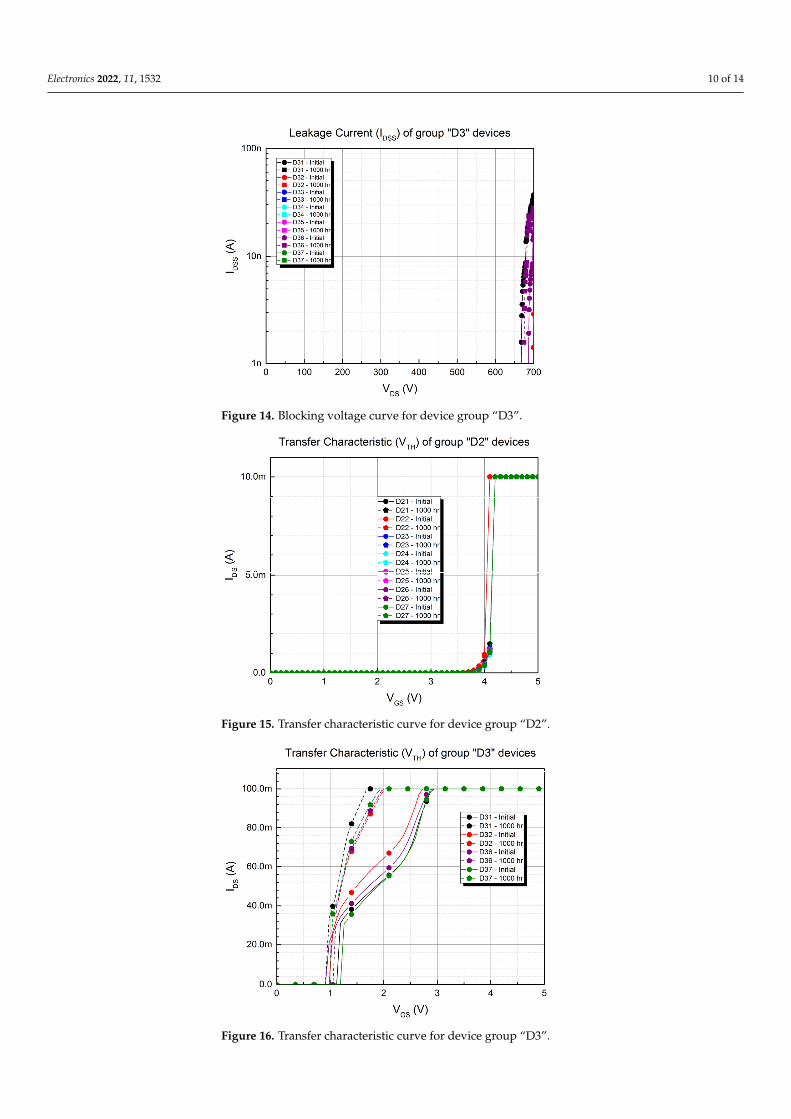
The remaining devices from groups “D2” and “D3” were characterized. Figures 13 and 14 show the blocking voltage curve for device groups “D2” and “D3”, respectively. The leakage current in the figures is consistent between testing. As shown in Figure 3, the leakage current from device groups “D2” and “D3” were constant throughout testing.
Figure 11. Drain–source resistance curve of device “D13”.
Electronics 2022, 11, 1532 9 of 14
Electronics 2022, 11, x FOR PEER REVIEW 9 of 15
Figure 11. Drain–source resistance curve of device “D13”.
Figure 12. Drain–source resistance curve of device “D17”.
The remaining devices from groups “D2” and “D3” were characterized. Figures 13 and 14 show the blocking voltage curve for device groups “D2” and “D3”, respectively. The leakage current in the figures is consistent between testing. As shown in Figure 3, the leakage current from device groups “D2” and “D3” were constant throughout testing.
Figure 12. Drain–source resistance curve of device “D17”.
The remaining devices from groups “D2” and “D3” were characterized. Figures 13and 14 show the blocking voltage curve for device groups “D2” and “D3”, respectively.The leakage current in the figures is consistent between testing. As shown in Figure 3, theleakage current from device groups “D2” and “D3” were constant throughout testing.
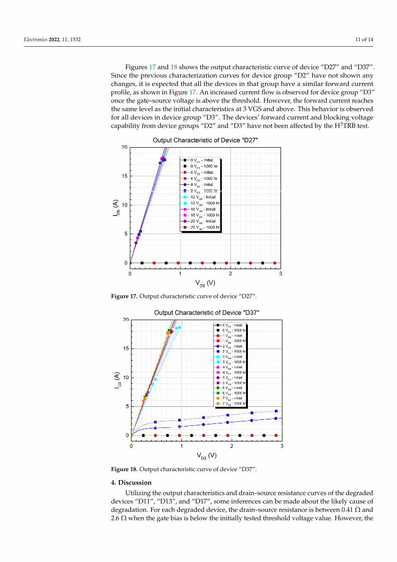
Figures 15 and 16 show the transfer characteristic curve for device groups “D2” and“D3”, respectively. The threshold voltage was measured with a compliance limit of 100 mAfor device group “D3”. The high compliance limit was set to the threshold voltage at 10mA following the datasheet specifications of device group D3, while the other two groupsspecified threshold voltage at 1 mA. While the threshold voltage curve for device group“D2” is consistent between testing, there was an increase in the rate of drain current fordevices “D31”, “D32”, “D36”, and “D37”. This increase in the current drain rate suggeststhat the transconductance has shifted. All devices from device group “D3” have minorthreshold voltage shifts up to 0.2 V, and both positive and negative shifts are observed.
Electronics 2022, 11, x FOR PEER REVIEW 10 of 15
Figure 13. Blocking voltage curve for device group “D2”.
Figure 14. Blocking voltage curve for device group “D3”.
Figures 15 and 16 show the transfer characteristic curve for device groups “D2” and “D3”, respectively. The threshold voltage was measured with a compliance limit of 100 mA for device group “D3”. The high compliance limit was set to the threshold voltage at 10 mA following the datasheet specifications of device group D3, while the other two groups specified threshold voltage at 1 mA. While the threshold voltage curve for device group “D2” is consistent between testing, there was an increase in the rate of drain current for devices “D31”, “D32”, “D36”, and “D37”. This increase in the current drain rate sug-gests that the transconductance has shifted. All devices from device group “D3” have mi-nor threshold voltage shifts up to 0.2 V, and both positive and negative shifts are observed.
Figure 13. Blocking voltage curve for device group “D2”.
Electronics 2022, 11, 1532 10 of 14
Electronics 2022, 11, x FOR PEER REVIEW 10 of 15
Figure 13. Blocking voltage curve for device group “D2”.
Figure 14. Blocking voltage curve for device group “D3”.
Figures 15 and 16 show the transfer characteristic curve for device groups “D2” and “D3”, respectively. The threshold voltage was measured with a compliance limit of 100 mA for device group “D3”. The high compliance limit was set to the threshold voltage at 10 mA following the datasheet specifications of device group D3, while the other two groups specified threshold voltage at 1 mA. While the threshold voltage curve for device group “D2” is consistent between testing, there was an increase in the rate of drain current for devices “D31”, “D32”, “D36”, and “D37”. This increase in the current drain rate sug-gests that the transconductance has shifted. All devices from device group “D3” have mi-nor threshold voltage shifts up to 0.2 V, and both positive and negative shifts are observed.
Figure 14. Blocking voltage curve for device group “D3”.
Electronics 2022, 11, x FOR PEER REVIEW 11 of 15
Figure 15. Transfer characteristic curve for device group “D2”.
Figure 16. Transfer characteristic curve for device group “D3”.
Figures 17 and 18 shows the output characteristic curve of device “D27” and “D37”. Since the previous characterization curves for device group “D2” have not shown any changes, it is expected that all the devices in that group have a similar forward current profile, as shown in Figure 17. An increased current flow is observed for device group “D3” once the gate–source voltage is above the threshold. However, the forward current reaches the same level as the initial characteristics at 3 VGS and above. This behavior is observed for all devices in device group “D3”. The devices’ forward current and blocking voltage capability from device groups “D2” and “D3” have not been affected by the H3TRB test.
Figure 15. Transfer characteristic curve for device group “D2”.
Electronics 2022, 11, x FOR PEER REVIEW 11 of 15
Figure 15. Transfer characteristic curve for device group “D2”.
Figure 16. Transfer characteristic curve for device group “D3”.
Figures 17 and 18 shows the output characteristic curve of device “D27” and “D37”. Since the previous characterization curves for device group “D2” have not shown any changes, it is expected that all the devices in that group have a similar forward current profile, as shown in Figure 17. An increased current flow is observed for device group “D3” once the gate–source voltage is above the threshold. However, the forward current reaches the same level as the initial characteristics at 3 VGS and above. This behavior is observed for all devices in device group “D3”. The devices’ forward current and blocking voltage capability from device groups “D2” and “D3” have not been affected by the H3TRB test.
Figure 16. Transfer characteristic curve for device group “D3”.
Electronics 2022, 11, 1532 11 of 14
Figures 17 and 18 shows the output characteristic curve of device “D27” and “D37”.Since the previous characterization curves for device group “D2” have not shown anychanges, it is expected that all the devices in that group have a similar forward currentprofile, as shown in Figure 17. An increased current flow is observed for device group “D3”once the gate–source voltage is above the threshold. However, the forward current reachesthe same level as the initial characteristics at 3 VGS and above. This behavior is observedfor all devices in device group “D3”. The devices’ forward current and blocking voltagecapability from device groups “D2” and “D3” have not been affected by the H3TRB test.
Electronics 2022, 11, x FOR PEER REVIEW 12 of 15
Figure 17. Output characteristic curve of device “D27”.
Figure 18. Output characteristic curve of device “D37”.
4. Discussion Utilizing the output characteristics and drain–source resistance curves of the de-
graded devices “D11”, “D13”, and “D17”, some inferences can be made about the likely cause of degradation. For each degraded device, the drain–source resistance is between 0.41 Ω and 2.6 Ω when the gate bias is below the initially tested threshold voltage value. However, the degraded drain–source resistance falls below the initial values once the gate bias surpasses the threshold voltage. This change in drain–source resistance indicates that the internal Si MOSFET is intact and that there is a secondary path between the gate and drain of the internal GaN HEMT that allows current flow when the device is in the off state. Transphorm and Q. Song et al. [9,23] observed and documented this short in their reliability testing and caused dielectric failure in the device when subject to a high electric field. The test conditions of the previous works are different from the presented work. However, all three cases subject the DUT to heat, either localized or from the environment,
Figure 17. Output characteristic curve of device “D27”.
Electronics 2022, 11, x FOR PEER REVIEW 12 of 15
Figure 17. Output characteristic curve of device “D27”.
Figure 18. Output characteristic curve of device “D37”.
4. Discussion Utilizing the output characteristics and drain–source resistance curves of the de-
graded devices “D11”, “D13”, and “D17”, some inferences can be made about the likely cause of degradation. For each degraded device, the drain–source resistance is between 0.41 Ω and 2.6 Ω when the gate bias is below the initially tested threshold voltage value. However, the degraded drain–source resistance falls below the initial values once the gate bias surpasses the threshold voltage. This change in drain–source resistance indicates that the internal Si MOSFET is intact and that there is a secondary path between the gate and drain of the internal GaN HEMT that allows current flow when the device is in the off state. Transphorm and Q. Song et al. [9,23] observed and documented this short in their reliability testing and caused dielectric failure in the device when subject to a high electric field. The test conditions of the previous works are different from the presented work. However, all three cases subject the DUT to heat, either localized or from the environment,
Figure 18. Output characteristic curve of device “D37”.
4. Discussion
Utilizing the output characteristics and drain–source resistance curves of the degradeddevices “D11”, “D13”, and “D17”, some inferences can be made about the likely cause ofdegradation. For each degraded device, the drain–source resistance is between 0.41 Ω and2.6 Ω when the gate bias is below the initially tested threshold voltage value. However, the

Electronics 2022, 11, 1532 12 of 14
degraded drain–source resistance falls below the initial values once the gate bias surpassesthe threshold voltage. This change in drain–source resistance indicates that the internalSi MOSFET is intact and that there is a secondary path between the gate and drain of theinternal GaN HEMT that allows current flow when the device is in the off state. Transphormand Q. Song et al. [9,23] observed and documented this short in their reliability testingand caused dielectric failure in the device when subject to a high electric field. The testconditions of the previous works are different from the presented work. However, all threecases subject the DUT to heat, either localized or from the environment, and a high electricfield due to a transient or static voltage bias. Based on the characteristic curves of thedegraded devices, it is believed that the failure mode observed in the degraded devices arelike the failure modes seen in [9,23].
Although the underlying cause for this failure is known, the results from the presentedwork still provide novel information on the long-term reliability of GaN HEMTs operat-ing in high humidity, high temperature environments. Similar failure modes have beenobserved in three different testing environments. The test conditions and time to failurereported by Transphorm are of interest for comparison due to using the same devices.Transphorm provides reliability data under High Temperature Reverse Bias (HTRB) testingfollowing the JEDEC standard JESD22-A108. The devices were biased at 520 V betweendrain and source with an operating temperature of 150 C. Transphorm tested 231 devicesfor qualification, with all devices passing after one thousand hours of testing [24]. Whencomparing the HTRB results presented by Transphorm to the presented work results, thereis a clear distinction between the number of device failures seen. The lower operatingtemperature of the H3TRB test should result in a significantly longer lifetime. However,more devices failed well before the one thousand hour mark indicating a different factor is adominant cause for equiree. With both tests being held to their respective JEDEC standard,the additional humidity component is the only substantial environmental factor. Thus,it is evident that the presence of high humidity drastically reduces the time to failure ofthe devices in group “D1”. The high humidity in the environment likely exacerbated thisfailure mode, as it increases the presence of mobile charges, such as Na+ and K+, for chargetrapping [25,26]. As humidity penetrates the packaging, positive mobile charges attach tothe passivation layer on the edge termination, enhancing the local electric field above thecritical field of the insulator to create a short [9,27].
Through analyzing the electrical characteristics of the DUTs, some inferences can bemade as to possible reasons why the high humidity did not cause any failures in devicegroup “D2”. The difference between the processing techniques of each manufactureris speculated to create a passivation layer that is less susceptible to defects caused bycharge trapping in high humidity environments. As the passivation layer degrades dueto charge trapping, these processing techniques influence the enhancements on localizedelectric fields and whether dielectric breakdown occurs. Such differences include passi-vation material and implementation of field rings. Simulation work was conducted byR. Natarajan et al. on different passivation materials for GaN HEMT devices and founddifferences in the electric field distribution, thus influencing the breakdown voltage [28].From a design perspective, increasing the number of field rings between the gate anddrain of the GaN HEMT would better shield the passivation from a high localized electricfield [29]. Further investigation into the device structure for device groups “D1” and “D2”is equireed.
Humidity is also expected to have changed the transfer characteristic curve for somedevices in device group “D3”. Unlike GaN cascode HEMTs, p-GaN are more prone tothreshold voltage instability issues [19,30–32] due to their Magnesium acceptors [19,31].Much of the reliability assessment for threshold voltage for wide-bandgap has been undera high temperature, gate bias (HTGB) test [33,34], or gate bias stress under characteriza-tion [30,32] for p-GaN HEMTs. Ultimately, performance degradation was not observed inthe device group “D3”.
Electronics 2022, 11, 1532 13 of 14
5. Conclusions
This paper evaluates commercial GaN devices under high humidity, high temperature,and high voltage accelerated tests. Twenty-one GaN HEMTs from three manufacturerswere tested at 85 C, 85%, while blocking voltage at 520 V for one thousand hours. Degra-dation was observed in three devices. Although two manufacturers used similar devicetopology, all degraded devices were from one manufacturer. The degraded devices couldnot block voltage, but their forward current capabilities were unaffected. It is suspectedthat the humidity has accelerated charge trapping in the degraded devices, resulting inhigher localized electric fields. It is speculated that the differences seen between devicegroups “D1” to “D2” are due to either a processing difference in the passivation layer ora design difference in the number of field rings. Future work includes failure analysisof the degraded devices through decapsulation to verify the failure mechanism and aninvestigation into the device structure of the devices.
Author Contributions: Conceptualization, S.B.B.; methodology, J.A.R.; data collection, J.A.R. and T.T.;formal analysis, J.A.R., T.T. and D.G.; writing—review and editing, J.A.R., T.T. and D.G.; supervision,S.B.B.; project administration, S.B.B.; funding acquisition, S.B.B. All authors have read and agreed tothe published version of the manuscript.
Funding: This research received no external funding.
Conflicts of Interest: The authors declare no conflict of interest.
References1. Lidow, A.; Strydom, J.; de Rooij, M.; Reusch, D. GaN Transistors For Efficient Power Conversion; John Wiley and Sons: West Sussex,
UK, 2015.2. Guacci, M.; Anderson, J.A.; Pally, K.L.; Bortis, D.; Kolar, J.W.; Kasper, M.J.; Deboy, G. Experimental Characterization of Silicon and
Gallium Nitride 200 V Power Semiconductors for Modular/Multi-Level Converters Using Advanced Measurement Techniques.IEEE J. Emerg. Sel. Top. Power Electron. 2020, 8, 2238–2254. [CrossRef]
3. Jafari, A.; Nikoo, M.S.; Perera, N.; Yildirim, H.K.; Karakaya, F.; Soleimanzadeh, R.; Matioli, E. Comparison of Wide-Band-GapTechnologies for Soft-Switching Losses at High Frequencies. IEEE Trans. Power Electron. 2020, 35, 12595–12600. [CrossRef]
4. Pushpakaran, B.N.; Subburaj, A.S.; Bayne, S.B. Commercial GaN-Based Power Electronic Systems: A Review. J. Electron. Mater.2020, 49, 6247–6262. [CrossRef]
5. Yang, W.; Yuan, J.-S.; Krishnan, B.; Shea, P. Characterization of Deep and Shallow Traps in GaN HEMT Using Multi-FrequencyC-V Measurement and Pulse-Mode Voltage Stress. IEEE Trans. Device Mater. Reliab. 2019, 19, 350–357. [CrossRef]
6. Hu, M.; Liu, G.; Du, E.; Mu, F. Thermal effect on dynamic Ron degradation of p-GaN AlGaN/GaN HEMTs on SiC substrates.IEICE Electron. Express 2020, 17, 20200255. [CrossRef]
7. Ray, W.B.; Schrock, J.A.; Bilbao, A.V.; Kelley, M.; Lacouture, S.; Hirsch, E.; Bayne, S.B. Analysis of GaN power MOSFET exporsureto pulsed overcurrents. In Proceedings of the IEEE Pulsed Power Conference (PPC), Austin, TX, USA, 31 May–4 June 2015;pp. 1–5. [CrossRef]
8. Li, H.; Li, X.; Wang, X.; Wang, J.; Alsmadi, Y.; Liu, L.; Bala, S. E-mode GaN HEMT short circuit robustness and degradation.In Proceedings of the IEEE Energy Conversion Congress and Exposition (ECCE), Cincinnati, OH, USA, 1–5 October 2017;pp. 1995–2002. [CrossRef]
9. Song, Q.; Zhang, R.; Kozak, J.P.; Liu, J.; Li, Q.; Zhang, Y. Failure Mechanisms of Cascode GaN HEMTs Under Overvoltage andSurge Energy Events. In Proceedings of the IEEE International Reliability Physics Symposium (IRPS), Monterey, CA, USA, 21–25March 2021; pp. 1–7. [CrossRef]
10. Song, S.; Munk-Nielsen, S.; Uhrenfeldt, C. How Can a Cutting-Edge Gallium Nitride High-Electron-Mobility Transistor EncounterCatastrophic Failure within the Acceptable Temperature Range? IEEE Trans. Power Electron. 2020, 35, 6711–6718. [CrossRef]
11. Cimmino, D.; Ferrero, S. High-Voltage Temperature Humidity Bias Test (HV-THB): Overview of Current Test Methodologies andReliability Performances. Electronics 2020, 9, 1884. [CrossRef]
12. Wang, N.; Cotton, I.; Evans, K. Impact of Thermal Cycling in Humid Environments on Power Electronic Modules. IEEE Trans.Compon. Packag. Manuf. Technol. 2012, 2, 1085–1091. [CrossRef]
13. Qiu, L.; Guzonas, D.A.; Qian, J. Corrosion of silicon nitride in high temperature alkaline solutions. J. Nucl. Mater. 2016, 476,293–301. [CrossRef]
14. Deng, H.; Meng, J.; Wang, D.-B.; Zhang, W. Breakdown Voltage Impact on Lifetime of 1200V IGBT modules under H3TRB-HVDCTesting. In Proceedings of the IEEE 26th International Symposium on Physical and Failure Analysis of Integrated Circuits (IPFA),Hangzhou, China, 2–5 July 2019; pp. 1–4. [CrossRef]
Electronics 2022, 11, 1532 14 of 14
15. Hoffmann, F.; Kaminski, N.; Schmitt, S. Investigation on the Impact of Environmental Stress on the Thermo- Mechanical Reliabilityof IGBTs by Means of Consecutive H3TRB and PCT Testing. In Proceedings of the 2021 33rd International Symposium on PowerSemiconductor Devices and ICs (ISPSD), Nagoya, Japan, 30 May–3 June 2021; pp. 371–374. [CrossRef]
16. Zorn, C.; Kaminski, N. Temperature–humidity–bias testing on insulated-gate bipolar transistor modules—Failure modes andacceleration due to high voltage. IET Power Electron. 2015, 8, 2329–2335. [CrossRef]
17. Dusmez, S.; Ali, S.H.; Heydarzadeh, M.; Kamath, A.S.; Duran, H.; Akin, B. Aging Precursor Identification and Lifetime Estimationfor Thermally Aged Discrete Package Silicon Power Switches. IEEE Trans. Ind. Appl. 2017, 53, 251–260. [CrossRef]
18. Brunko, A.; Gloth, M.; Kaminski, N. Humidity Capability of Enhancement Mode GaN High Electron Mobility Transistors. InProceedings of the IEEE 8th Workshop on Wide Bandgap Power Devices and Applications (WiPDA), Redondo Beach, CA, USA,7–11 November 2021; pp. 242–245. [CrossRef]
19. Meneghini, M.; Hilt, O.; Wuerfl, J.; Meneghesso, G. Technology and Reliability of Normally-Off GaN HEMTs with p-Type Gate.Energies 2017, 10, 153. [CrossRef]
20. Transphorm. TP65H035WS Datasheet. Available online: https://www.transphormusa.com/en/document/datasheet-tp65h035ws-650v-gan-fet/ (accessed on 22 April 2022).
21. Nexpedia. GAN063-650WSA Datasheet. Available online: https://assets.nexperia.com/documents/data-sheet/GAN063-650WSA.pdf (accessed on 22 April 2022).
22. GaN Systems. GS-065-030-2-L Datasheet. Available online: https://gansystems.com/wp-content/uploads/2021/08/GS-065-030-2-L-DS-Rev-210630.pdf (accessed on 22 April 2022).
23. Transphorm. GaN for Automotive Applications. Available online: https://www.transphormusa.com/ja/document/autoreliabilityfaq-transphorm/ (accessed on 22 April 2022).
24. Barr, R. Qualification Report TPH65H035WS. Available online: https://www.transphormusa.com/en/document/qualification-report-tp65h035ws/ (accessed on 22 April 2022).
25. Ohring, M.; Kasprzak, L. Reliability and Failure of Electronic Materials and Devices Second Edition; Elsevier: Amsterdam, TheNetherlands, 2014.
26. Sigel, A.; Sigel, H.; Sigel, R.K.O. The Alkali Metal Ions: Their Role for Life; Springer: Berlin, Germany, 2016.27. Matsushima, H.; Yamada, R.; Shima, A. Two Mechanisms of Charge Accumulation in Edge Termination of 4H-SiC Diodes Caused
by High-Temperature Bias Stress and High-Temperature and High-Humidity Bias Stress. IEEE Trans. Electron Devices 2018, 65,3318–3325. [CrossRef]
28. Natarajan, R.R.; Parthasarathy, E.; Murugapandiyan, P. Influence of High-k Passivation Layer on Gate Field Plate Al-GaN/GaN/AlGaN Double Heterojunction HEMT. Silicon 2022, 14, 1–9. [CrossRef]
29. Nezar, A.; Salama, C.A.T. Breakdown voltage in LDMOS transistors using internal field rings. IEEE Trans. Electron Devices 1991,38, 1676–1680. [CrossRef]
30. Efthymiou, L.; Murukesan, K.; Longobardi, G.; Udrea, F.; Shibib, A.; Terrill, K. Understanding the Threshold Voltage InstabilityDuring OFF-State Stress in p-GaN HEMTs. IEEE Electron Device Lett. 2019, 40, 1253–1256. [CrossRef]
31. Tallarico, A.N.; Stoffels, S.; Posthuma, N.; Decoutere, S.; Sangiorgi, E.; Fiegna, C. Threshold Voltage Instability in GaN HEMTswith p-Type Gate: Mg Doping Compensation. IEEE Electron Device Lett. 2019, 40, 518–521. [CrossRef]
32. Guo, H.; Gong, H.; Shao, P.; Yu, X.; Wang, J.; Wang, R.; Zheng, Y. Over 1200 V Normally-OFF p-NiO Gated AlGaN/GaN HEMTson Si with a Small Threshold Voltage Shift. IEEE Electron Device Lett. 2022, 43, 268–271. [CrossRef]
33. Habersat, D.B.; Lelis, A.J.; Green, R. Towards a Robust Approach to Threshold Voltage Characterization and High TemperatureGate Bias Qualification. In Proceedings of the IEEE International Reliability Physics Symposium (IRPS), Dallas, TX, USA,28 April–30 May 2020; pp. 1–4. [CrossRef]
34. Meneghini, M.; Rossetto, I.; Bisi, D.; Ruzzarin, M.; Van Hove, M.; Stoffels, S.; Zanoni, E. Negative Bias-Induced Threshold VoltageInstability in GaN-on-Si Power HEMTs. IEEE Electron Device Lett. 2016, 37, 474–477. [CrossRef]