Linear and nonlinear-optical properties of GaN thin films
10
Vol. 10, No. 8/August 1993/J. Opt. Soc. Am. B 1447 Linear- and nonlinear-optical properties of GaN thin films J. Miragliotta, D. K. Wickenden, T. J. Kistenmacher, and W A. Bryden Applied Physics Laboratory,The Johns Hopkins University, Johns Hopkins Road, Laurel, Maryland 20723-6099 Received December 7, 1992 Results of a linear- and nonlinear-optical investigation of GaN thin films epitaxially deposited onto (0001)- oriented sapphire are reported. Wavelength- and angle-dependent linear transmission measurements were used to determine the thickness and the refractive index in the 500-1200-nm spectral region for a series of six GaN films. Analysis of angle-dependent, second-harmonic (SH) transmission profiles at 532 nm provided a quantitative evaluation of x..), X.-, and x- and a determination of the GaN lattice structure and tilt angle between the optical axis of the film and the surface normal of the sample. Dispersion effects between 500 nm and 1.064 m prevented efficient SH production in individual GaN films that were greater than 2.5 Am in thickness. However, field calculations on a proposed multilayer GaN-sapphire structure observed a ninefold increase in the transmitted SH power as compared with a single GaN film. 1. INTRODUCTION Gallium nitrade (GaN) is a wide-band-gap, III-V compound semiconductor that crystallizes in a hexagonal wurzite structure. During the past decade research pertaining to the growth and preparation of metal nitride thin films has culminated in the development of crystalline samples with nonconventional deposition techniques such as metal or- ganic chemical vapor deposition (MOCVD) and magnetron sputtering.`14 The renewed experimental activity re- garding the material characterization of this metal nitride is in part due to the direct band gap of -3.4 eVin undoped GaN, which can be tailored for the production of tunable electro-optic devices in the UV and visible wavelength range of the spectrum when this material is alloyed with either AlN or InN. However, the development of photonic devices such as UV LED's and laser diodes has been ham- pered by the inability to produce GaN samples that pos- sess the electronic properties (mobility, etc.) required for commercial application. 56 During this recent development period little attention has been given to the characterization of the optical prop- erties of GaN thin films. Unlike the electronic proper- ties, which are degraded by crystal defects such as gain boundaries, nitrogen vacancies, and unintentionally intro- duced impurities, the linear-optical parameters such as the refractive index are much less sensitive to these im- perfections. In addition, the noncentrosymmetric struc- ture of the GaN crystal makes this material capable of generating a second-order nonlinear-optical response, such as second-harmonic (SH) generation, from the bulk region of the crystal. In fact the optical nonlinearity of the ma- terial provides a source for noninvasive, analytical investi- gations of the crystalline structure and orientation. From a technological viewpoint there are numerous nonlinear optical applications, e.g., optical communications and fre- quency conversion, that rely on second-order optical non- linearities. 79 Despite these potentials, only a handful of nonlinear-optical investigations have been performed on GaN thin films, and little has been reported on the pos- sible applications for all-optical devices. In this paper we report the results of a linear- and nonlinear-optical investigation of a number of GaN thin films that were grown on the (0001) surface of a sapphire substrate in a MOCVD reactor. The transmitted SH power from the GaN-sapphire samples was found to pos- sess a sensitivity to the quality of the crystal structure and orientation of the GaN film relative to that of the underlying sapphire substrate. The combination of lin- ear- and nonlinear-optical transmission measurements permitted a determination of the wavelength-dependent refractive index from 500 to 1200 nm, the film thickness, and the magnitude of the nonlinear susceptibility elements for a series of six GaN films. In addition the angular dependence of the SH response permitted a determination of the misalignments between the surface normal of the sample and the optical axis of the GaN film. Analysis of the optical results showed no appreciable variation in ei- ther the refractive index or the nonlinear susceptibility tensor elements for the GaN samples ranging in thickness from 0.74 to 5.3 Am; however, there was a considerable decrease in the SH peak intensity as the film thickness was increased beyond 2.5 Am owing to the short coherence length (-3 /Lm)in GaN in the visible and near-IR wave- length region. Despite the phase-matching limitation in the GaN films, the magnitudes of the nonlinear coeffi- cients were found to be at least an order of magnitude larger than those of KDP or crystalline quartz. In Section 2 a brief review of the electromagnetic the- ory used to model the nonlinear-optical response of thin films is presented. This subject has received consider- able attention for more than three decades,1 0 - 2 and only those issues pertinent to this investigation are presented. A detailed section on the experimental procedure, describ- ing the epitaxial growth technique, film characterization, and optical measurements, precedes the presentation of the optical results and discussion. A comparison of these results with earlier nonlinear investigations, both experi- mental and theoretical, is presented in the Results and Discussion section. Finally, a hypothetical nonlinear de- vice composed of alternating GaN and linear dielectric films illustrates an enhancing mechanism for the SH con- version efficiency for nonlinear materials that are limited by a short coherence length. 0740-3224/93/081447-10$06.00 © 1993 Optical Society of America Miragliotta et al.
Transcript of Linear and nonlinear-optical properties of GaN thin films
Vol. 10, No. 8/August 1993/J. Opt. Soc. Am. B 1447
Linear- and nonlinear-optical properties of GaN thin films
J. Miragliotta, D. K. Wickenden, T. J. Kistenmacher, and W A. Bryden
Applied Physics Laboratory, The Johns Hopkins University, Johns Hopkins Road, Laurel, Maryland 20723-6099
Received December 7, 1992
Results of a linear- and nonlinear-optical investigation of GaN thin films epitaxially deposited onto (0001)-oriented sapphire are reported. Wavelength- and angle-dependent linear transmission measurements wereused to determine the thickness and the refractive index in the 500-1200-nm spectral region for a series of sixGaN films. Analysis of angle-dependent, second-harmonic (SH) transmission profiles at 532 nm provided aquantitative evaluation of x..), X.-, and x- and a determination of the GaN lattice structure and tilt anglebetween the optical axis of the film and the surface normal of the sample. Dispersion effects between 500 nmand 1.064 m prevented efficient SH production in individual GaN films that were greater than 2.5 Am inthickness. However, field calculations on a proposed multilayer GaN-sapphire structure observed a ninefoldincrease in the transmitted SH power as compared with a single GaN film.
1. INTRODUCTION
Gallium nitrade (GaN) is a wide-band-gap, III-V compoundsemiconductor that crystallizes in a hexagonal wurzitestructure. During the past decade research pertaining tothe growth and preparation of metal nitride thin films hasculminated in the development of crystalline samples withnonconventional deposition techniques such as metal or-ganic chemical vapor deposition (MOCVD) and magnetronsputtering.`14 The renewed experimental activity re-garding the material characterization of this metal nitrideis in part due to the direct band gap of -3.4 eV in undopedGaN, which can be tailored for the production of tunableelectro-optic devices in the UV and visible wavelengthrange of the spectrum when this material is alloyed witheither AlN or InN. However, the development of photonicdevices such as UV LED's and laser diodes has been ham-pered by the inability to produce GaN samples that pos-sess the electronic properties (mobility, etc.) required forcommercial application.5 6
During this recent development period little attentionhas been given to the characterization of the optical prop-erties of GaN thin films. Unlike the electronic proper-ties, which are degraded by crystal defects such as gainboundaries, nitrogen vacancies, and unintentionally intro-duced impurities, the linear-optical parameters such asthe refractive index are much less sensitive to these im-perfections. In addition, the noncentrosymmetric struc-ture of the GaN crystal makes this material capable ofgenerating a second-order nonlinear-optical response, suchas second-harmonic (SH) generation, from the bulk regionof the crystal. In fact the optical nonlinearity of the ma-terial provides a source for noninvasive, analytical investi-gations of the crystalline structure and orientation. Froma technological viewpoint there are numerous nonlinearoptical applications, e.g., optical communications and fre-quency conversion, that rely on second-order optical non-linearities.7 9 Despite these potentials, only a handful ofnonlinear-optical investigations have been performed onGaN thin films, and little has been reported on the pos-sible applications for all-optical devices.
In this paper we report the results of a linear- and
nonlinear-optical investigation of a number of GaN thinfilms that were grown on the (0001) surface of a sapphiresubstrate in a MOCVD reactor. The transmitted SHpower from the GaN-sapphire samples was found to pos-sess a sensitivity to the quality of the crystal structureand orientation of the GaN film relative to that of theunderlying sapphire substrate. The combination of lin-ear- and nonlinear-optical transmission measurementspermitted a determination of the wavelength-dependentrefractive index from 500 to 1200 nm, the film thickness,and the magnitude of the nonlinear susceptibility elementsfor a series of six GaN films. In addition the angulardependence of the SH response permitted a determinationof the misalignments between the surface normal of thesample and the optical axis of the GaN film. Analysis ofthe optical results showed no appreciable variation in ei-ther the refractive index or the nonlinear susceptibilitytensor elements for the GaN samples ranging in thicknessfrom 0.74 to 5.3 Am; however, there was a considerabledecrease in the SH peak intensity as the film thicknesswas increased beyond 2.5 Am owing to the short coherencelength (-3 /Lm) in GaN in the visible and near-IR wave-length region. Despite the phase-matching limitation inthe GaN films, the magnitudes of the nonlinear coeffi-cients were found to be at least an order of magnitudelarger than those of KDP or crystalline quartz.
In Section 2 a brief review of the electromagnetic the-ory used to model the nonlinear-optical response of thinfilms is presented. This subject has received consider-able attention for more than three decades,10-2 and onlythose issues pertinent to this investigation are presented.A detailed section on the experimental procedure, describ-ing the epitaxial growth technique, film characterization,and optical measurements, precedes the presentation ofthe optical results and discussion. A comparison of theseresults with earlier nonlinear investigations, both experi-mental and theoretical, is presented in the Results andDiscussion section. Finally, a hypothetical nonlinear de-vice composed of alternating GaN and linear dielectricfilms illustrates an enhancing mechanism for the SH con-version efficiency for nonlinear materials that are limitedby a short coherence length.
0740-3224/93/081447-10$06.00 © 1993 Optical Society of America
Miragliotta et al.
1448 J. Opt. Soc. Am. B/Vol. 10, No. 8/August 1993
Air
VOkinf
GaN SapphireSubstrate
z=O z=df
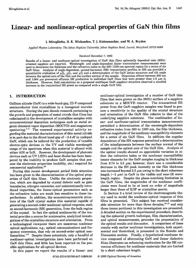
Fig. 1. Schematic of SHG in a thin GaN film on a sapphire sub-strate. The wave vectors of each field are discussed in the text.The refracted angle for the transmitted beams is exaggerated.Only the harmonic fields are shown in the film and sapphire sub-strate. The unit vectors x and 2 define the plane of incidence.The unit vector y points out of the page and is along the GaNsurface.
2. THEORY
In previous treatments of the nonlinear electromagneticresponse of a thin dielectric film at frequency 2 to anincident light source of frequency w, tractable solutions ofMaxwell's equations for nonlinear media were deducedsuch that the usual boundary conditions for the fields atthe plane interfaces between the nonlinear and the linearmedia were satisfied. These solutions were obtained bygeneralizing the laws of reflection and refracton to in-clude nonlinear source terms, which were induced in thefilm at frequency 2w. This procedure permitted the con-struction of generalized Fresnel formulas for the evalu-ation of the intensity and the field polarization conditionsof the transmitted and the reflected harmonic beams.Detailed discussions of this nonlinear-optical problem forthin films can be found in Refs. 10, 13, and 14.
An illustration of the experimental sample under inves-tigation is shown in Fig. 1. In this schematic a linearlypolarized field at frequency wo is incident upon a GaN-airinterface at angle 61 and is transmitted into the film atangle 02 = 0,. The plane of incidence is defined as thex-z plane. We have attempted to account for optical ef-fects that are related to the spatial quality of the experi-mental light source; we do so by incorporating a Gaussianbeam profile into the incident beam,'" 5 i.e.,
Eincw(x, y)
(2Cos 01 2 [ y\21E0 exp[-(x - df tan 0e2x)2 - \W/
(1)
where E0 is the magnitude of the incident field, w is theradius of the Gaussian beam at the focus (waist), the x-yplane defines the surface of the GaN film, and df is thethickness of the film. The linear field in the film (notshown) can induce a nonlinear polarization wave that
propagates with wave vector k8(2&w) = 2k2 (0)), wherek2 (0)) is the wave vector of the transmitted linear field.In addition to this inhomogeneous wave, a free harmonicwave is generated at the surface of the nonlinear slab withwave vector kf (2w), as is shown in Fig. 1. The total har-monic field in the film is a superposition of these twoterms. Since the direction and the magnitude of thewave vectors of these respective fields are not equal unlessnf(w) = nf(2w), the free and the driven harmonic waveswill propagate with different phase velocities in the film.The phase difference leads to an interference betweenthese fields, which manifests itself as an oscillatory behav-ior in the transmitted SH signal as the optical path lengthin the nonlinear material is varied. Thus, for efficientgeneration of harmonic power, the difference between theindex at the fundamental and the harmonic frequenciesmust be negligible. This can be accomplished in materialsthat are negatively birefringent, such as KDP crystal, butphase matching in GaN is prohibited owing to the positiveuniaxial nature of the refractive index in this material.
For the specific crystal symmetry of GaN (6mm) theinduced nonlinear polarization in the metal nitride filmhas the following form in Cartesian coordinates1 31 6:
P(,(22E) =X2X.lz, (2 )Ez,(w) Ex,(Q
Py,(2co) = 2XXZ,(2)E'(Q)Ey(&),
PzY2(2w) = 2 x2 '(2)[E () 2 + E(w) 2] + x5't'(2)E(w) 2
(2)
where Xxzx, Xz'xtx, and Xz'z' are the nonzero elements in thesecond-order nonlinear susceptibility tensor. For anideal wurzite structure these elements are not indepen-dent and are geometrically related by the expressions 7
Xx'ztx = Xz'xx', Xz'xx' = -Xzzz/ 2 . (3)
The primes in the expressions for the induced nonlinearpolarization denote the response viewed in the coordinateframe of the crystal (x', y', z') and not with respect to thelaboratory coordinate system (optical frame in Fig. 1).For evaluation of the nonlinear response in the laboratorycoordinate system, the expressions in Eqs. (2) were trans-formed from the crystal into the optical coordinate systemby use of orthogonal matrices constructed from the Eulerangles between the two respective reference frames.' 8
The transformation procedure was tedious but straight-forward and permitted the nonlinear polarization compo-nents in the laboratory frame to be described by thefollowing expressions:
i-X', y', z
p(2) = E Ayp 2)i-x',y',z
plab = AziPixtli-x',yz
where Aij are the transformation tensor elements thatcontained the rotational information relating the two co-ordinate frames (xtal stands for crystal). Note that the2w notation has been omitted on all harmonic polarization
(4)
Miragliotta et al.

Vol. 10, No. 8/August 1993/J. Opt. Soc. Am. B 1449
and field terms. The expressions in Eqs. (4) are directlydependent on the transformation between the crystal andthe laboratory reference frame, permitting informationconcerning the orientational relationship between theGaN thin film and the sapphire substrate to be deducedfrom the SH transmitted intensity.
In the present investigation x-ray analysis of the GaNfilms determined that the direction of the optical axis forall films (z' direction in the crystal frame) was within 30of the surface normal of the sample (z direction in theoptical or laboratory frame). Under these orientationalconditions the off-diagonal elements of Aij are negligible,and the diagonal terms are nearly unity. Therefore thelaboratory and the crystal frames of reference are nearlycoincident with one another, i.e.,
p (2)b _ (2) a
= lab pytal. (5)
used as the source terms in the transmitted harmonicfield in the thin film.
The calculational guideline of the preceding discussionprovides a procedure for determining the solutions toMaxwell's equation in a nonlinear thin film bound by lin-ear media. Included in the model are the existence ofmultiple reflections for the linear and the nonlinear fieldsat the two GaN interfaces, since both the linear and thenonlinear transmission data in Section 4 suggest theirpresence. The underlying substrate is considered to haveno second-order nonlinearity (as was verified experimen-tally). With the above-mentioned considerations, the har-monic field transmitted into the sapphire substrate (fieldsk l and k2 in Fig. 1) is
E,2"(x,y) = vr[Ajg(x) + Bih(x)][(COS 2 [ y \21)< expl -21 exp - -I
L \ Wo / L Wo /(7)
where
g(x) = exp{- 2 [df(tan Of)(cos 01) 2 exp [4dfx(tan f)(COS2 01)]
h df (tan 02)(cos 01) 2} e 4dfx(tan 02)(cos2 01)hWx = exp -2L w expL w2
[n,(cos Of) + nf(cos Ot)][Qlnf + Q2(cos Of)]
(nf cos O)(nt cos Of)- exp( _i,f)[nf(cos O - nt(cos Of)][Q2 (CoS Of) - Qlnf]
(nf cos Ot)(n, cos Of)
[nf (cos t)- nt(cos Of)][Qlnf + Q2 (cos Of)]exp(if) [nt(cos of) + nf(cos O0)][Q2(cos Of) - Qlnf]exp(-if)l
D(nf cos Ot)(nt cos Of) D(nf cos Ot)(nt cos Of)
X {[n,(cos Of) - nf(cos Or)][nf(cos O) + nt(cos Of)]exp(ikf) + [nf(cos Ot) - n(cos Of)]
X [n,(cos Of) + nf(cos O,)]exp(-ikf)},
2(Q3 nt + Q4 cos Ot) _ 2[Q4 (cos O) - Q3nt] f[nf(cos ot) - n(cos 0)][nt(cos Of) + nf(cos O)]exp(i'kf)
nt cos t nt cos Ot L'
+ [nf(cos O) - nt(cos Of)][nfr(cos Of) + nf(cos 0,)]exp(-iof)}DJ
D
(10)
In general an accurate determination of the thin-film ori-entation from the nonlinear response will require knowl-edge of the transformation angles between the crystal andthe laboratory frames, as is demonstrated in Section 4;however, the dependence of the induced polarization inthe laboratory frame can now be estimated from the ex-pressions shown in Eqs. (2).
In this experimental investigation all measurementsused optical excitation geometries, which led to the effi-cient generation of onlyp-polarized SH signals, i.e., Plb0. For the purpose of constructing an analytical expres-sion for the transmitted SH field, the p-polarized nonlin-ear polarization can be decomposed into components thatare either along [pjt2)] or perpendicular to [P)] the direc-tion of propagation:
P2= P(2 (cos O) + P(2)(sin Os),
p( 2) = _p(2)(sin O) + p5(2)(COS 0), (6)
where O, is the transmitted angle of the nonlinear sourcefield in the GaN film. The expressions in Eqs. (6) are
with
D = [nf(cos O0 - nt(cos Of)][nr(cos Of) - nf(cos Or)]
X exp(iof) + [nf(cos Ot) + nt(cos Of)]
X [nr(cos Of) + nf(cos Or)]exp(-i40f). (11)
In these expressions the terms Qj contain the inducednonlinear polarization in the film and are given by theexpressions
(cos O 8)P( (sin O)P¶2fQ1(3)= 2 2 2fls - flf nfl
(12)
where the subscript 1(3) indicates that pjt2) and p(2) in theexpression were evaluated at z = 0(df), and
(13)(2)
Q2(4) - 2'nl - fl
where the subscript 2(4) indicates that p(2) in this expres-sion is evaluated at z = 0(df). The index n, denotes therefractive index of the nonlinear source term and is equal
Al = -exp(io,
(8)
B1 =
(9)
Miragliotta et al.
1450 J. Opt. Soc. Am. B/Vol. 10, No. 8/August 1993
to nff(w). In these expressions the refractive indiceslabeled nr, nf, and nt are evaluated at 2X. On the refrac-tive-index, cosine, and sine terms the subscripts 1, t, r,respectively, refer to the incident, the film, the transmit-ted, and the reflected media. The terms f representsthe phase of the free harmonic wave as it propagates fromthe front to the back of the film, i.e.,
O = 2nf'wdf(cos Of)/c, (14)
where co is the fundamental frequency and c is the speedof light in vacuum. Since the source terms propagatewith a phase velocity that is proportional to the index ofthe film at co, the expressions in Eqs. (7)-(11) demonstratethat multiplication of the Qi and of terms will lead to aninterference profile in the transmitted SH signal owing tothe phase mismatch.
The harmonic field that is transmitted across thesapphire-air interface (k1 and k2' in Fig. 1) contains aFresnel factor that takes into account the effects of linearreflection and refraction at this linear interface. In de-termining the transmitted SHG power across the sampleinterface, we have integrated the harmonic intensity ofthis beam,
I2 . x (Et 2)*(Et 2.) (15)
over the sapphire-air interface and normalized this quan-tity to the power and the beam area of the incident excita-tion source. The expression for the normalized SH poweris given by
= F1(A1*A + B*B + (A,*B + B*A,)
X exp{~ (df cos 01)2[(tan 02) - (tan Of)]2) (
where F, is the Fresnel factor that accounts for transmis-sion of the SH intensity across the sapphire-air interface:
[ 2nt cos O 12F=[nt(cos 0) + n(cos O) J(7
In the expression for SH transmitted power, the asteriskdenotes the complex conjugate of that quantity. The ex-ponential term in Eq. (16) describes the effects that arisewhen a Gaussian is used rather than a plane-wave spatialprofile. This correction factor also accounts for the dis-persion differences in the free and the bound waves andthe finite size of the beam diameter. For the samples ex-amined in this investigation the thicknesses of the GaNfilms were such that df << w and 02 (W) Of(2 Q). There-fore the exponential function is -1 and has no significanteffect on the generation of a SH signal in these samples.
An examination of Eq. (7)-(11) shows that the film pa-rameters required for numerical analysis of SH transmis-sion data include the refractive index of the material at oand 2, the film thickness df, the Euler angles that relatethe crystal and the optical reference frames, and the non-vanishing nonlinear coefficients. Although the algebraicexpression in Eq. (16) is rather cumbersome, it representsa tractable solution to the nonlinear response of a thinfilm. In practice one can extract the nonlinear coeffi-cients from the experimental second-harmonic generation
(SHG) data by first determining the film's thickness andrefractive index from linear transmission or reflectionstudies.
3. EXPERIMENTAL PROCEDUREA primary limitation in the technological development ofbulk GaN is the difficulty of obtaining crystalline mate-rial at reasonable temperatures and pressures. To over-come this problem, techniques such as MOCVD have beendeveloped for the preparation of heteroepitaxial films,which are usually deposited on the (0001) surface of sap-phire. The GaN films used in this study were grown inan Emcore vertical spinning-disk MOCVD reactor operat-ing at a base pressure of 70 Torr. Source materials forfilm growth were trimethyl gallium and ammonia (NH),which were transported to the reactor in a nitrogen car-rier gas.' Before film growth, x-ray diffraction resultsshowed that the surface normal of the sapphire substrateswere oriented to within 3 of the (0001) direction. Thechemically polished substrates were cleaned in hotHNO :H2 02 :H2 0 and HCl:H2 02 :H2 0 solutions. Thispreparation procedure has been found to ensure epitaxialgrowth of GaN on (0001) sapphire.
Before initiation of continuous film growth, we prede-posited a GaN nucleation layer onto the substrate by heat-ing the sample to 600'C and exposing it to the sourcematerials for 50 s. Inclusion of this layer resulted in asignificant improvement in the surface morphology of thesubsequent growth layer, which was deposited at a sub-strate temperature of 1100 'C. We achieved the variationin film thickness by varying the sample's time of exposureto the source materials, which typically yielded a 1-2-,um/h growth rate. After growth the epitaxial relation-ship and duality of the films were verified by additionalx-ray diffraction measurements. The single-crystal filmswere oriented with the (0001) plane of the film parallel tothe (0001) plane of the substrate and a 30' azimuthal rota-tion of the GaN layer with respect to the underlying sap-phire substrate, i.e., the (1010) plane of the film wasparallel to the (1120) plane of the substrate.
We performed a series of linear-optical transmissionmeasurements to determine the refractive index and filmthickness of the GaN films. Normal-incidence lineartransmission in the spectral range of 500-1200 nm wasmeasured with a Perkin-Elmer 330 UV/visible spectrome-ter. In addition, angle-dependent linear transmissioncurves at 514.5 nm for light polarized parallel (p polar-ized) and perpendicular (s polarized) to the plane of inci-dence were generated for each GaN-sapphire sample byuse of a Spectra-Physics 164AC Ar' laser as the incidentlight source.
We performed SHG measurements by measuring thetransmitted SH signal from a GaN-sapphire sample as afunction of the incident angle and the field polarization ofthe fundamental and the SH beam. This procedure isidentical to the Maker-fringe transmission technique.""9
In this technique the intensity envelope and generatedfringes in the SHG transmission profile provide an accu-rate means for determining the magnitude of the nonvan-ishing elements in the nonlinear susceptibility tensor andthe orientation of the optical axis of the film. Q-switchedradiation from a Nd:YAG pulsed laser at 1.064 m was
Miraghiotta et al.
Vol. 10, No. 8/August 1993/J. Opt. Soc. Am. B 1451
used as the optical source for the SH experiments (Contin-uum NY82-10, -7-ns pulse width, 10-Hz repetition rate,and single-longitudinal-mode operation). Before inci-dence the beam was passed through a silica plate beamsplitter for the purpose of creating a reference beam forthe SHG sample measurements. The sample beam wasspectrally filtered to remove residual 532-nm light andwas focused to a 1-mm spot (Gaussian profile) on the GaNsurface with an energy density of 10 mJ/cm2 . A half-wave plate was placed in the incident beam for the purposeof selecting either s- or p-polarized incident radiation.The transmitted light from the sample was filtered to re-move 1.064-,um light with appropriate color filters, ana-lyzed with a linear polarizer, and detected with an EMI9789QB photomultiplier tube. We verified the harmonicnature of the sample signal by demonstrating its quadraticdependence on the incident 1.064-,um intensity. The ref-erence IR beam was transmitted through a KDP crystalwhose nonlinearity generated a SH signal that was easilydetected with a Scientech photodiode. The current out-puts of the photomultiplier tube and photodiode were ana-lyzed with separate gated integrators, and all data storageand analysis was performed with a Macintosh IIfx com-puter. We removed fluctuations in the sample signal aris-ing from intensity variations in the incident beam bynormalizing this signal to the SH signal generated in theKDP reference. Following the SHG measurements oneach GaN sample, the angular dependence of the SH sig-nal from a quartz reference crystal was determined. Thenonlinear coefficient of this material has been character-ized from earlier SHG studies20 and provides an accuratemeans for determining the absolute magnitude of the non-linear coefficients of the GaN film.
Sample rotation for all angle-dependent measurementswas accomplished with a computer-interfaced steppingmotor. Data collection was synchronized to the samplerotation and was processed by the computer interface ev-ery 0.50 as the sample was rotated ±750 about an axisalong the sample surface (y axis in Fig. 1). For the pulsedlaser studies each data point represents a 10-pulse average.Numerical analysis of the linear and the SH transmissionmeasurements was accomplished with a least-squaresnonlinear curve-fitting routine.
4. RESULTS AND DISCUSSION
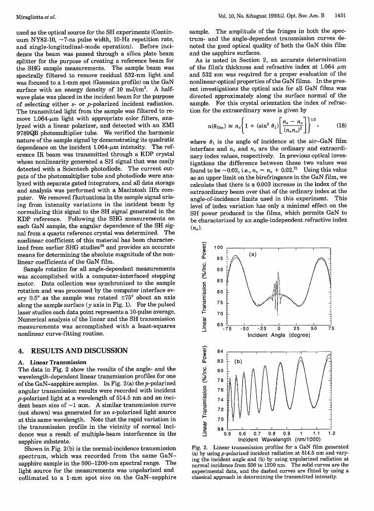
A. Linear TransmissionThe data in Fig. 2 show the results of the angle- and thewavelength-dependent linear transmission profiles for oneof the GaN-sapphire samples. In Fig. 2(a) thep-polarizedangular transmission results were recorded with incidentp-polarized light at a wavelength of 514.5 nm and an inci-dent beam size of -1 mm. A similar transmission curve(not shown) was generated for an s-polarized light sourceat this same wavelength. Note that the rapid variation inthe transmission profile in the vicinity of normal inci-dence was a result of multiple-beam interference in thesapphire substrate.
Shown in Fig. 2(b) is the normal-incidence transmissionspectrum, which was recorded from the same GaN-sapphire sample in the 500-1200-nm spectral range. Thelight source for the measurements was unpolarized andcollimated to a 1-mm spot size on the GaN-sapphire
sample. The amplitude of the fringes in both the spec-trum- and the angle-dependent transmission curves de-noted the good optical quality of both the GaN thin filmand the sapphire surfaces.
As is noted in Section 2, an accurate determinationof the film's thickness and refractive index at 1.064 ,umand 532 nm was required for a proper evaluation of thenonlinear-optical properties of the GaN films. In the pres-ent investigations the optical axis for all GaN films wasdirected approximately along the surface normal of thesample. For this crystal orientation the index of refrac-tion for the extraordinary wave is given by
n(Ofiim) no{1 + (sin2 ol) n2 (18)
where 0, is the angle of incidence at the air-GaN filminterface and n. and ne are the ordinary and extraordi-nary index values, respectively. In previous optical inves-tigations the difference between these two values wasfound to be -0.02, i.e., ne = n0 + 0.02.21 Using this valueas an upper limit on the birefringence in the GaN film, wecalculate that there is a 0.003 increase in the index of theextraordinary beam over that of the ordinary index at theangle-of-incidence limits used in this experiment. Thislevel of index variation has only a minimal effect on theSH power produced in the films, which permits GaN tobe characterized by an angle-independent refractive index(ne).
030
C
C0
._
CnI0
.EtoC
C
1 00
95
90
85
80
75
70
65
Incident Angle (degree)
a)
00
0CnCn.EC
a)
84
82
80
78
76
74
72
70
68j 0.5 0.6 0.7 0.8 0.9 1 1.1 1.2
Incident Wavelength (nm/1000)Fig. 2. Linear transmission profiles for a GaN film generated(a) by using p-polarized incident radiation at 514.5 nm and vary-ing the incident angle and (b) by using unpolarized radiation atnormal incidence from 500 to 1200 nm. The solid curves are theexperimental data, and the dashed curves are fitted by using aclassical approach in determining the transmitted intensity.
Miragliotta et al.
1452 J. Opt. Soc. Am. B/Vol. 10, No. 8/August 1993
Table 1. Film Thickness and Curve-FittingParameters Used in the Cauchy Dispersion
Formula for Determining the Refractive Index ofthe GaN Films
Film Thickness (um) Parameter A Parameter B
1 0.74 2.271 0.0322 1.09 2.267 0.0333 1.30 2.264 0.0344 2.25 2.303 0.0345 3.00 2.289 0.0396 5.31 2.268 0.034
A classical electromagnetic treatment was used in mod-eling the linear response of the thin film in both theangle- and the wavelength-dependent linear transmissioncurves.22 In the analysis the thickness of each film wasevaluated from the s- and the p-polarized angle-dependentlinear transmission data. With this value substitutedinto the electromagnetic equations for the transmitted op-tical power from the thin film, the normal-incidencetransmission scan was similarly analyzed to yield thewavelength-dependent refractive index. In both calcula-tions previously published results were used for thewavelength-dependent refractive index of the sapphiresubstrate.23 With regard to the refractive index of theGaN samples, the transparent nature of the films (mini-mal absorption) in this spectral range permits thisparameter to be described by the well-known Cauchy dis-persion formula2 2
nf = A + (B/Ainc2), (19)
where the results for parameters A and B as well as thethicknesses for the six films are listed in Table 1. In theseries of films investigated in this paper the index of re-fraction was determined to be 2.29 ± 0.02 at 1.064 mand 2.40 ± 0.02 at 532 nm, which is consistent with theresults for GaN thin films previously reported in Ref. 21.Examples of the excellent curve-fitting results for the an-gular and wavelength linear transmission data are in-cluded with the experimental data in Fig. 2 (dashedcurves).
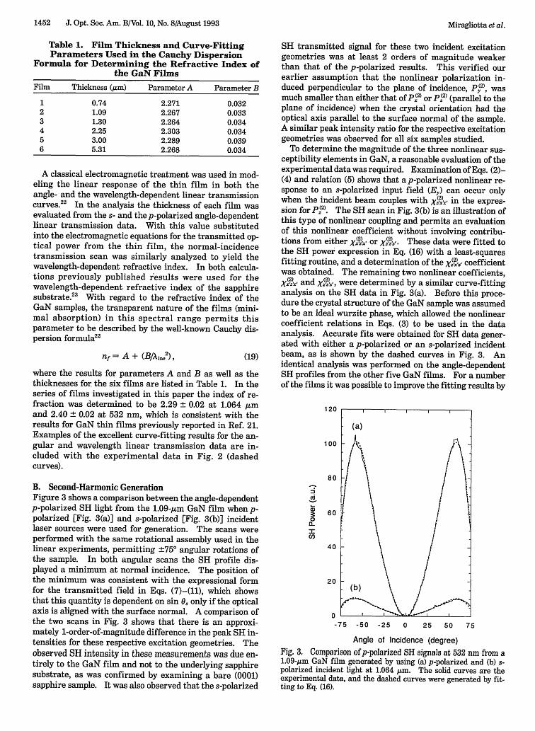
B. Second-Harmonic GenerationFigure 3 shows a comparison between the angle-dependentp-polarized SH light from the 1.09-Am GaN film when p-polarized [Fig. 3(a)] and s-polarized [Fig. 3(b)] incidentlaser sources were used for generation. The scans wereperformed with the same rotational assembly used in thelinear experiments, permitting ±75° angular rotations ofthe sample. In both angular scans the SH profile dis-played a minimum at normal incidence. The position ofthe minimum was consistent with the expressional formfor the transmitted field in Eqs. (7)-(11), which showsthat this quantity is dependent on sin O only if the opticalaxis is aligned with the surface normal. A comparison ofthe two scans in Fig. 3 shows that there is an approxi-mately 1-order-of-magnitude difference in the peak SH in-tensities for these respective excitation geometries. Theobserved SH intensity in these measurements was due en-tirely to the GaN film and not to the underlying sapphiresubstrate, as was confirmed by examining a bare (0001)sapphire sample. It was also observed that the s-polarized
SH transmitted signal for these two incident excitationgeometries was at least 2 orders of magnitude weakerthan that of the p-polarized results. This verified ourearlier assumption that the nonlinear polarization in-duced perpendicular to the plane of incidence, pr2), wasmuch smaller than either that of pI) or p(2 ) (parallel to theplane of incidence) when the crystal orientation had theoptical axis parallel to the surface normal of the sample.A similar peak intensity ratio for the respective excitationgeometries was observed for all six samples studied.
To determine the magnitude of the three nonlinear sus-ceptibility elements in GaN, a reasonable evaluation of theexperimental data was required. Examination of Eqs. (2)-(4) and relation (5) shows that a p-polarized nonlinear re-sponse to an s-polarized input field (Ey) can occur onlywhen the incident beam couples with x(), in the expres-sion for P 2). The SH scan in Fig. 3(b) is an illustration ofthis type of nonlinear coupling and permits an evaluationof this nonlinear coefficient without involving contribu-tions from either x(2)x or I.Y. These data were fitted tothe SH power expression in Eq. (16) with a least-squaresfitting routine, and a determination of the XzYxAx coefficientwas obtained. The remaining two nonlinear coefficients,x.i2. and Yz', were determined by a similar curve-fittinganalysis on the SH data in Fig. 3(a). Before this proce-dure the crystal structure of the GaN sample was assumedto be an ideal wurzite phase, which allowed the nonlinearcoefficient relations in Eqs. (3) to be used in the dataanalysis. Accurate fits were obtained for SH data gener-ated with either a p-polarized or an s-polarized incidentbeam, as is shown by the dashed curves in Fig. 3. Anidentical analysis was performed on the angle-dependentSH profiles from the other five GaN films. For a numberof the films it was possible to improve the fitting results by
1 20
1 00
80
0ICO
60
40
20
0 L--75 -50 -25 0 25 50 75
Angle of Incidence (degree)Fig. 3. Comparison of p-polarized SH signals at 532 nm from a1.09-Am GaN film generated by using (a) p-polarized and (b) s-polarized incident light at 1.064 j.m. The solid curves are theexperimental data, and the dashed curves were generated by fit-ting to Eq. (16).
Miragliotta et al.
Vol. 10, No. 8/August 1993/J. Opt. Soc. Am. B 1453
Table 2. Nonlinear Coefficients (Normalizedto u in Quartz), Coherence Lengths, and Tilt
Angles for the GaN FilmsFilm X'zx' Xz'x Xz'z'z' (m) 0 (deg)
1 11.03 10.56 -22.06 3.10 -3.412 11.33 11.33 -22.66 3.04 0.003 11.69 11.33 -23.38 2.92 -2.704 10.40 10.84 -20.82 2.94 3.975 11.20 11.03 -22.40 2.58 3.476 11.99 12.01 -23.98 2.95 3.64
choosing X(2x) to be independent of x~A' and Xz') but keep-ing the relation between x4YA' and XzYZ~Z' intact. The firstassumption allowed for the possibility of structural per-turbations in the crystal that led to a distortion in theideal wurzite structure. With regard to the second crite-rion, we observed that the contribution from the xz21, termin Eqs. (3) was considerably weaker than that of Xxz'xA-This was due to the coupling dependence of X"Z)z on the zcomponent of the transmitted field in the film, which hada maximum value of only 0.4Efilm(W) for the range ofincident angles used in this experimental investigation.Although the nonlinear response from Xz' was not negli-gible, the weaker contribution to the overall SH signal ledto unrealistic variations (50%) in the parameter duringthe SH curve-fitting analysis of a number of GaN films.A list of the nonlinear coefficients for the six GaN films isshown in Table 2. The magnitudes of these terms arenormalized to the Xyxx' susceptibility element in crystal-line quartz. For all films the nonlinearities were at least1 order of magnitude greater than the nonlinear coeffi-cient in quartz. There was very little variation (<5%) inthe nonlinear coefficients in the six films; the relationshipbetween these terms was close to that for the ideal wurz-ite structure.
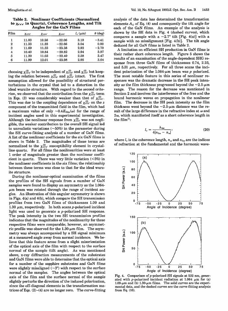
During the nonlinear-optical examination of the filmsthe profiles of the SH signals from a number of GaNsamples were found to display an asymmetry as the 1.064-,m beam was rotated through the range of incident an-gles. An illustration of this angular asymmetry is shownin Figs. 4(a) and 4(b), which compare the SH transmissionprofiles from two GaN films of thicknesses 1.09 and1.30 ,um, respectively. In both scans p-polarized incidentlight was used to generate a p-polarized SH response.The peak intensity in the two SH transmission profilesindicates that the magnitudes of the nonlinearity for theserespective films were comparable; however, an asymmet-ric profile was observed for the 1.30-um film. The asym-metry was always accompanied by a SH signal minimumat a measured angle away from normal incidence. We be-lieve that this feature arose from a slight misorientationof the optical axis of the film with respect to the surfacenormal of the sample (tilt angle). As was mentionedabove, x-ray diffraction measurements of the substratesand GaN films were able to determine that the optical axisfor a number of the sapphire substrates and GaN filmswere slightly misaligned (3°) with respect to the surfacenormal of the samples. The angles between the opticalaxis of the film and the surface normal of the sampleslightly perturbs the direction of the induced polarization,since the off-diagonal elements in the transformation ma-trices of Eqs. (2)-(4) are no longer zero. The curve-fitting
analysis of the data has determined the transformationelements Aij of Eq. (4) and consequently the tilt angle foreach of the GaN films. An example of the analysis isshown by the SH data in Fig. 4 (dashed curves), whichcompares a sample with a 2.7° tilt [Fig. 4(a)] with asample with no misalignment [Fig. 4(b)]. The tilt anglededuced for all GaN films is listed in Table 2.
A limitation on efficient SH production in GaN films istheir rather short coherence length. Figure 5 shows theresults of an examination of the angle-dependent SHG re-sponse from three GaN films of thicknesses 0.74, 2.25,and 5.31 m, respectively. For all three scans the inci-dent polarization of the 1.064-pum beam was p polarized.The most notable feature in this series of nonlinear re-sponses was the dramatic decrease in the SH peak inten-sity as the film thickness progressed beyond the -2.5-Amrange. The reason for the decrease was mentioned inSection 2 and involves the interference of the free and thebound harmonic waves on propagation in the nonlinearfilm. The decrease in the SH peak intensity as the filmthickness went beyond the -2.5-nm distance was the re-sult of the large difference in the refractive index at w and2w, which manifested itself as a short coherence length inthe film":
C, = In k-Ainc
41n,, - n,,|I(20)
where 1, is the coherence length, n<,, and n2,,, are the indicesof refraction at the fundamental and the harmonic wave-
1 20
1 00
C'i
a)
a-ICO,
80
60
40
20
0 -75
1 50
a-
ICO
100
50
-50 -25 0 25 50 75Angle of Incidence (degree)
-75 -50 -25 0 25 50 75Angle of Incidence (degree)
Fig. 4. Comparison of p-polarized SH signals at 532 nm, gener-ated with p-polarized incident radiation at 1.064 m for (a)1.09-,m and (b) 1.30-,m films. The solid curves are the experi-mental data, and the dashed curves are the curve fitting analysisfrom Eq. (16).
0 -
Miragliotta et al.

1454 J. Opt. Soc. Am. B/Vol. 10, No. 8/August 1993
250
200
Sqa
0a-CD
1 50
1 00
50 ok ,
0 -
-75 -50 -25 0 25 50 75
Angle of Incidence (degree)Fig. 5. Comparison of p-polarized SH signals at 532 nm, gener-ated with p-polarized incident radiation at 1.064 Ium for (a) 0.74-,(b) 2.25-, and (c) 5.31-Ium GaN films. The solid curves are theexperimental data, and the dashed curves are the curve fittinganalysis from Eq. (16).
lengths, respectively, and Ainc is the incident wavelength.This parameter has a significant effect on harmonic gen-eration in the GaN films, as is illustrated in the SH trans-mission curves for the 2.25- and 5.31-/gLm films. For bothfilms analysis of the SH data obtained nonlinear coeffi-cients of approximately the same magnitude (Table 2).However, the interference between the free and the boundharmonic waves in the thicker film led to a significantlyreduced SH signal versus that of the thinner film.Table 2 lists the normal-incidence optical coherence lengthfor each film. Note that all films have a coherence lengththat is in the range 2.5-3 m.
As is mentioned in the Introduction, nonlinear-opticalinvestigations of GaN thin films are not extensive. Atheoretical approach that was developed in the early1970's relates the nonlinearity of the crystal to the degreeof excess charge in the bonding region of a covalentbond.'7' 24-25 The approach lends itself to a quantitative, ifsomewhat approximate, analysis for III-V semiconductorcompounds and has been successfully applied to a numberof wurzite and zinc-blende materials. In the model thebond charge tends to be highly mobile and thus highly po-larizable. The linear polarizability of the bond arisesfrom the motion of the bond charge, which is influencedby the degree of electronegativity (heteropolar) and thedifference in atomic radii of the bonded atoms (homo-polar). The nonlinear polarizability results from thefield-induced changes in the linear susceptibility, which isdependent on the spatial displacement of the bond chargeby the applied optical field. As derived by Levine,'7 thefield-induced displacement depends on the average energygap between the bonding and antibonding levels in thetwo-atom bond, which is simply the sum of the individualenergy gaps related to the homopolar and heteropolar con-
tributions of the bond (in this case between Ga and N).The nonlinear polarizability is derived by differentiatingthe linear polarizability with respect to the component ofthe applied field along the bond axis. An attractivefeature of the bond-charge model is the a priori determi-nation of the critical parameters of the nonlinear polariz-ability. These parameters are determined entirely fromthe linear response, i.e., susceptibility, and thus no adjust-able parameters are required for a solution of xI". In de-termination of the nonlinear susceptibility, the crystal istreated as being constructed out of the identical, cylindri-cally symmetric bonds, where bond-bond interactions inthe solid are neglected. The nonlinear susceptibility isobtained by summing all individual polarizabilities in-duced on the bonds between the various atoms in the lat-tice. In Levine's calculations for GaN an estimate ofthese parameters permitted a determination of the hetero-polar and homopolar nonlinearities, which were 52 x 10-9and -115 x 10-9 esu, respectively, giving a total of-63 10-9 esu for d33, which is equivalent to X(2Z) /2.This value was estimated to be approximately -50 timesthe calculated and experimental value of quartz20 (1.2 X10⁻⁹ esu). Levine mentioned that the GaN nonlinearitywas an approximate value because of the lack of goodrefractive-index values for GaN. We believe that the ratioof approximately -22 between X"Z2') in GaN and x.xYx inquartz observed in the present investigation is within thelimits of the earlier theoretical calculations. In additionto the magnitude of the nonlinearities, the good fit to theexperimental data achieved by using the geometric rela-tionships in Eq. (3) for the three nonlinear coefficients in-dicated that the tetrahedral structure of the unit cell waslargely undistorted in the GaN structure.
Comparison with previous experimental studies of epi-taxial GaN films showed that the magnitude of the non-linearities in this investigation were approximately fourtimes smaller than that observed from earlier SH mea-surements.26 27 In these earlier reports no attempt wasmade to determine the refractive indices of the films be-fore the nonlinear examination and analysis. The linearproperties of the GaN film were chosen a priori from ear-lier optical studies and used in the field calculations,which determined the nonlinear coefficients. In our in-vestigation the expression for the SH power in Eqs. (16)was found to be extremely sensitive to the difference inthe refractive index at the fundamental and the harmonicfrequencies. Thus an a priori determination of theseparameters could lead to a significant error in the even-tual determination of the nonlinear coefficients. We be-lieve that our approach in evaluating the linear propertiesbefore the nonlinear analysis provided a more accurate de-termination of the nonlinear coefficients.
It is possible to enhance the SH efficiency in GaN filmsby creating multilayer structures that are composed of al-ternating layers of GaN and a transparent linear dielectricmaterial. A theoretical examination of harmonic genera-tion from multilayer nonlinear structures was examinedby Bethune for both isotropic28 and anisotropic2 9 (GaN)materials. The alternating nonlinear-linear structurediffers from these earlier treatments in that the linear di-electric layer provides a phase shift between the transmit-ted fundamental and SH fields as they propagate betweenthe nonlinear layers. The phase shift allows the SH field
Miragliotta et al.
Vol. 10, No. 8/August 1993/J. Opt. Soc. Am. B 1455
10
0
E
0
0
00
0 5 1 o 1 5 20 25 30 35 40
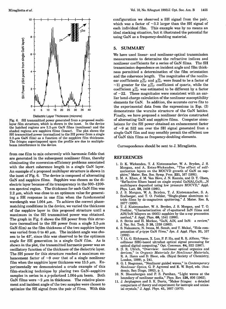
Dielectric Layer Thickness (microns)Fig. 6. SH transmitted power generated from a proposed multi-layer film structure, which is shown in the inset. In the devicethe hatched regions are 2.2-/,um GaN films (nonlinear) and theshaded regions are sapphire films (linear). The plot shows theSH transmitted power (normalized to the SH power from a single2.2-,um GaN film) as a function of the sapphire film thickness.The fringes superimposed upon the profile are due to multiple-beam interference in the device.
from one film to mix coherently with harmonic fields thatare generated in the subsequent nonlinear films, therebyeliminating the conversion-efficiency problems associatedwith the short coherence length in a single GaN layer.An example of a proposed multilayer structure is shown inthe inset of Fig. 6. The device is composed of alternatingGaN and sapphire films. Sapphire was chosen as the di-electric layer because of its transparency in the 500-12 00-nm spectral region. The thickness for each GaN film was2.2 Amm, which was close to an optimum value for generat-ing a SH response in one film when the fundamentalwavelength was 1.064 Aum. To achieve the correct phase-matching conditions in the device, we varied the thicknessof the sapphire layer in this proposed structure until amaximum in the SH transmitted power was obtained.The graph in Fig. 6 shows the SH power from this struc-ture (normalized to the SH power from a single 2.2-/.LmGaN film) as the film thickness of the two sapphire layerswas varied from 0 to 40 ,tm. The incident angle was cho-sen to be 45°, since this was observed to be the optimumangle for SH generation in a single GaN film. As isshown in the plot, the transmitted harmonic power was anoscillatory function of the thickness of the dielectric layer.The SH power for this structure reached a maximum en-hancement factor of 9 over that of a single nonlinearfilm when the sapphire layer thickness was 13.5 Aum. Ex-perimentally we demonstrated a crude example of thisfilm-stacking technique by placing two GaN-sapphiresamples in series in a p-polarized 1.064-,Am beam. BothGaN films were-2 ,um in thickness. The relative place-ment and incident angle of the two samples were chosen tooptimize the SH signal from the pair of films. With this
configuration we observed a SH signal from the pair,which was a factor of -3.2 larger than the SH signal ofeach individual film. This example was by no means anideal stacking situation, but it illustrated the potential forusing GaN as a frequency-doubling material.
5. SUMMARY
We have used linear- and nonlinear-optical transmissionmeasurements to determine the refractive indices andnonlinear coefficients for a series of GaN films. The SHtransmission dependence on incident angle and film thick-ness permitted a determination of the film orientationand the coherence length. The magnitudes of the nonlin-ear coefficients xad and X(' were found to be a factor of-11 greater for the X(- coefficient of quartz, while thecoefficient XZZ was estimated to be different by a factorof -22. These magnitudes were consistent with an ear-lier bond-charge calculation of the nonlinear susceptibilityelements for GaN. In addition, the accurate curve fits tothe experimental data from the expressions in Eqs. (3)demonstrate the wurzite structure of the GaN lattice.Finally, we have proposed a nonlinear device constructedof alternating GaN and sapphire films. Computer simu-lations for the SH power obtained an enhancement factorof -9 at 532 nm over the SH signal generated from asingle GaN film and may sensibly permit the efficient useof GaN thin films as frequency-doubling elements.
Correspondence should be sent to J. Miragliotta.
REFERENCES
1. D. K. Wickenden, T. J. Kistenmacher, W A. Bryden, J. S.Morgan, and A. Estes-Wickenden, "The effect of self-nucleation layers on the MOCVD growth of GaN on sap-phire," Mater. Res. Soc. Symp. Proc. 221, 167 (1991).
2. M. A. Khan, J. M. Van Hove, J. N. Kuznia, and D. T. Olsen,"Reflective filters based on single crystal GaN/AlGaN,-,Nmultilayers deposited using low pressure MOCVD," Appl.Phys. Lett. 59, 2408 (1991).
3. J. S. Morgan, W A. Bryden, T. J. Kistenmacher, S. A.Ecelberger, and T. 0. Poehler, "Single-phase aluminum ni-tride films by dc-magnetron sputtering," J. Mater. Res. 5,2677 (1990).
4. T. J. Kistenmacher, W A. Bryden, J. S. Morgan, and T. 0.Poehler, "Characterization of rf-sputtered InN films andAlN/InN bilayers on (0001) sapphire by the x-ray precessionmethod," J. Appl. Phys. 68, 1541 (1990).
5. S. Strite and H. Morkoc, "GaN, AlN, and InN: a review,"J. Vac. Sci. Tech. B 10, 1238 (1992).
6. S. Nakamura, N. Iwasa, M. Senoh, and T. Mukai, "Hole com-pensation of p-type GaN films," Jpn. J. Appl. Phys. 31, 107(1992).
7. Y. Li, G. Eichmann, X. Luo, P. P. Ho, and R. R. Alfano, "Non-collinear SHG-based ultrafast optical signal processing foroptical digital computing," Opt. Commun. 64, 322 (1987).
8. D. R. Ulrich, "Overview: nonlinear optical organics anddevices," in Organic Materials for Nonlinear Materials,R. A. Hann and D. Bloor, eds. (Royal Society of Chemistry,London, 1989), p. 241.
9. G. I. Stegeman, "Nonlinear guided waves," in ContemporaryNonlinear Optics, G. P. Agrawal and R. W Boyd, eds. (Aca-demic, San Diego, 1992), p. 1.
10. N. Bloembergen and P. S. Pershan, "Light waves at theboundary of nonlinear media," Phys. Rev. 128, 606 (1962).
11. J. Jerphagnon and S. K. Durtz, "Maker fringes: a detailedcomparison of theory and experiment for isotropic and uniax-ial crystals," J. Appl. Phys. 41, 1667 (1970).
Miragliotta et al.

1456 J. Opt. Soc. Am. B/Vol. 10, No. 8/August 1993
12. Y. Hase, K. Kumata, S. S. Kano, M. Ohashi, T. Kondo, R. Ito,and Y. Shiraki, "New method for determining the nonlinearoptical coefficients of thin films," Appl. Phys. Lett. 61, 145(1992).
13. Y R. Shen, Principles of Nonlinear Optics, 1st ed. (Wiley,New York, 1984), Chap. 2.
14. N. Bloembergen, Nonlinear Optics (Benjamin-Cummings,New York, 1965), Chap. 4.
15. G. D. Boyd, H. Kasper, and J. H. McFee, "Linear and nonlin-ear optical properties of AgGaS2, CuGaS2, and CuInS2, andtheory of the wedge technique for the measurement of nonlin-ear coefficients," IEEE J. Quantum Electron. QE-7, 563(1971).
16. R. Boyd, Nonlinear Optics (Academic, San Diego, Calif.,1992), Chap. 1.
17. B. F. Levine, "Bond-charge calculation of nonlinear opticalsusceptibilities for various crystal structures," Phys. Rev. B7, 2600 (1973).
18. H. Goldstein, Classical Mechanics, 2nd ed. (Addison-Wesley,Reading, Mass., 1981), Chap. 4.
19. P. D. Maker, R. W Terhune, M. Nisenoff, and C. M. Savage,"Effects of dispersion and focusing on the production of opti-cal harmonics," Phys. Rev. Lett. 8, 21 (1962).
20. M. Choy and R. L. Byer, 'Accurate second-order measure-
Miragliotta et al.
ments of visible and infrared nonlinear of crystals," Phys.Rev. B 14, 1693 (1976).
21. E. Ejder, Phys. Status Solidi A 6, 442 (1971).22. M. Born and E. Wolf, Principles of Optics, 6th ed. (Perga-
mon, New York, 1980).23. I. H. Malitson, "Refraction and dispersion of synthetic sap-
phire," J. Opt. Soc. Am. 52, 1377 (1962).24. B. F. Levine, 'A new contribution to the nonlinear optical sus-
ceptibility arising from unequal atomic radii," Phys. Rev.Lett. 25, 440 (1970).
25. B. F. Levine, "d-Electron effects on bond susceptibilities andionicities," Phys. Rev. B 7, 2591 (1973).
26. I. M. Catalano, A. Cingolani, M. Lugara, and A. Minafra,"Nonlinear optical properties of GaN," Opt. Commun. 23,419 (1977).
27. T. Ishidate, K. Inoue, and M. Aoki, "SHG of epitaxially-grownGaN crystal," Jpn. J. Appl. Phys. 19, 1641 (1980).
28. D. S. Bethune, "Optical harmonic generation and mixing inmultilayer media: analysis using optical matrix tech-niques," J. Opt. Soc. Am. B 6, 910 (1989).
29. D. S. Bethune, "Optical harmonic generation and mixing inmultilayer media: extension of optical transfer matrix ap-proach to include anisotropic materials," J. Opt. Soc. Am. B8, 367 (1991).