Doping-related broadening of the density of states governs ...
Upload
independentCategory
view
4download
0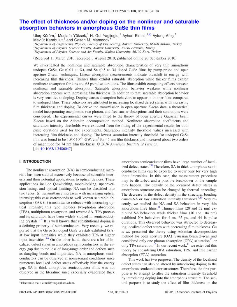
The effect of thickness and/or doping on the nonlinear and saturableabsorption behaviors in amorphous GaSe thin films
Ulaş Kürüm,1 Mustafa Yüksek,1 H. Gul Yaglioglu,1 Ayhan Elmali,1,a� Aytunç Ateş,2
Mevlüt Karabulut,3 and Gasan M. Mamedov3
1Department of Engineering Physics, Faculty of Engineering, Ankara University, 06100 Ankara, Turkey2Department of Physics, Science Faculty, Atatürk University, 25240 Erzurum, Turkey3Department of Physics, Science and Art Faculty, Kafkas University, 36100 Kars, Turkey
�Received 11 March 2010; accepted 3 August 2010; published online 20 September 2010�
We investigated the nonlinear and saturable absorption characteristics of very thin amorphousundoped GaSe, Ge �0.01 at. %�, and Sn �0.5 at. %� doped GaSe films by pump-probe and openaperture Z-scan techniques. Linear absorption measurements indicate blueshift in energy withincreasing film thickness. Thinner films exhibit saturable absorption while thicker films exhibitnonlinear absorption for 4 ns and 65 ps pulse durations. The films exhibit competing effects betweennonlinear and saturable absorption. Saturable absorption behavior weakens while nonlinearabsorption appears with increasing film thickness. In addition to that, saturable absorption behavioris very sensitive to doping. Doping causes absorption behaviors to appear in thinner films comparedto undoped films. These behaviors are attributed to increasing localized defect states with increasingfilm thickness and doping. To derive the transmission in open aperture Z-scan data, a theoreticalmodel incorporating one photon, two photon, and free carrier absorptions and their saturations wereconsidered. The experimental curves were fitted to the theory of open aperture Gaussian beamZ-scan based on the Adomian decomposition method. Nonlinear absorption coefficients andsaturation intensity thresholds were extracted from the fitting of the experimental results for bothpulse durations used for the experiments. Saturation intensity threshold values increased withincreasing film thickness and doping. The lowest saturation intensity threshold for undoped GaSefilm was found to be 1.9�10−3 GW /cm2 for 45 nm film thickness and increased about two ordersof magnitude for 74 nm film thickness. © 2010 American Institute of Physics.�doi:10.1063/1.3486047�
I. INTRODUCTION
The nonlinear absorption �NA� in semiconducting mate-rials has been studied extensively because of scientific inter-ests and their potential applications to optical devices. Theseapplications include Q-switching, mode-locking, upconver-sion lasing, and optical limiting. NA can be classified intotwo types: �i� transmittance increases with increasing opticalintensity; this case corresponds to well known saturable ab-sorption �SA�; �ii� transmittance reduces with increasing op-tical intensity; this type includes two-photon absorption�TPA�, multiphoton absorption, and reverse SA. TPA processand its saturation have been widely studied in semiconduct-ing crystals.1–4 It is well known that substitutional doping isa defining property of semiconductors. Very recently, we re-ported that the Ge or Sn doped GaSe crystals exhibited �SA�at low input intensities while they exhibited TPA at higherinput intensities.5,6 On the other hand, there are a lot of lo-calized defect states in amorphous semiconductors in the en-ergy gap due to the loss of long-range order and defects suchas dangling bonds and impurities. NA in amorphous semi-conductors can be observed at nonresonant conditions sincenumerous localized defect states effectively blur the energygap. SA in thick amorphous semiconductor films was notobserved in the literature since especially evaporated thick
amorphous semiconductor films have large number of local-ized defect states.7,8 Therefore, SA in thick amorphous semi-conductor films can be expected to occur only for very highinput intensities. In this case, the measurement proceduremay be disturbed and a possible breakdown of the samplemay happen. The density of the localized defect states inamorphous structure can be changed by thermal annealing.The decrease in the defect density in the structural bondingcauses SA or low saturation intensity threshold.9,10 Very re-cently, we studied the NA and SA behaviors in very thinamorphous InSe films.11 Thinner films �20 and 52 nm� ex-hibited SA behaviors while thicker films �70 and 104 nm�exhibited NA behaviors for 4 ns, 65 ps, and 44 fs pulsedurations. This observed behavior was attributed to decreas-ing localized defect states with decreasing film thickness. Guet al. presented the theory using Adomian decompositionmethod for open aperture �OA� Gaussian beam Z-scan andconsidered only one photon absorption �OPA� saturation12 oronly TPA saturation.13 In our recent work,11 we extended thistheory by considering OPA saturation, TPA, and free carrierabsorption �FCA� saturation.
This work has two purposes. The density of the localizeddefect states can also be altered by introducing doping to theamorphous semiconductor structures. Therefore, the first pur-pose is to attempt to alter the saturation intensity thresholdby introducing doping into the amorphous structure. The sec-ond purpose is to study the effect of film thickness on thea�Electronic mail: [email protected].
JOURNAL OF APPLIED PHYSICS 108, 063102 �2010�
0021-8979/2010/108�6�/063102/8/$30.00 © 2010 American Institute of Physics108, 063102-1

that saturation intensity threshold in another amorphoussemiconductor other than InSe.11 In order to see the effect ofdoping, we chose undoped GaSe, 0.01 at. % Ge doped GaSe�GaSe:Ge� and 0.5 at. % Sn doped GaSe �GaSe:Sn� amor-phous semiconductor thin films. Besides, we studied the ef-fect of the film thickness on the saturation behavior by pre-paring very thin single layer amorphous films �between 38and 74 nm�. We investigated the NA and SA properties withOA Z-scan technique at 1064 nm for 4 ns or 65 ps pulsedurations. Bulk GaSe consists of Se–Ga–Ga–Se tetralayersheets, separated by a relatively large gap, and having onlyweak van der Waals interactions holding the Se–Ga–Ga–Setetralayer sheets to each other. Bulk GaSe is an indirect bandgap semiconductor having a 2.11 eV direct band gap.14,15
II. EXPERIMENT
Amorphous thin films were prepared by using bulk un-doped GaSe, Ge �0.01 at. %�, and Sn �0.5 at. %� doped GaSecrystals which were grown using conventional Bridgman–Stochbarger method.5,6 Fused silica substrates were cleanedthoroughly in deionized water in an ultrasonic bath for 2 h.They were dried in flowing nitrogen to remove native oxide,and placed immediately on a substrate holder. After this pro-cess, GaSe thin films were deposited on fused silica sub-strates at room temperature by vacuum evaporation tech-nique at 8�10−6 Torr. The film thicknesses weredetermined by using spectroscopic ellipsometer �Woollam,-M2000V� in the photon energy range from 1.24 to 3.34 eV�from 999 to 370 nm�. All spectra were taken at three anglesof incidence �60°, 65°, and 70°� to increase the fitting accu-racy. Thicknesses of thin films were determined using theWoollam Co. WVASE32™ software package. The structuralanalysis of the films were carrier out by using XRD tech-nique varying the diffraction angle 2�=20° –80° range usingCu K� radiation. The XRD spectra revealed that all thin filmsexhibited amorphous behavior as seen previously in the lit-erature for GaSe films deposited with the same technique.9,16
The absorption spectra of the GaSe, GaSe:Ge, and GaSe:Sn
films were taken using a UV-Vis absorption spectrophotom-eter �Shimadzu UV-1800�. An uncoated fused silica substratewas used as a reference.
The atomic force microscope �AFM� measurementswere performed to analyze the surface morphology of theGaSe thin films. The images were obtained using PSIA XE-100E atomic force microscope with resolutions in the 2 nmrange in noncontact mode �force constant �0.2 N /m andresonance frequency �13 kHz� and XEI 1.6 Image Process-ing Program.
NA of amorphous films were measured by using OAZ-scan technique as described in the literature.17 In order tosee the effect of different mechanisms contributing the non-linear response of the films, two laser sources with nanosec-ond and picosecond pulse durations were used for the experi-ments. These laser sources are; �1� Q-switched Nd:YAGlaser with 4 ns pulse duration, 1064 nm �1.16 eV� wave-length, and 10 Hz repetition rate �Quantel Brillant�. �2�Q-switched Nd:YAG laser with 65 ps pulse duration, 1064nm �1.16 eV� wavelength, and 10 Hz repetition rate �Con-tinuum Leopard SV�.
Transmission pump-probe spectroscopy technique isused to understand the NA mechanism. Ti:sapphire laseramplifier-optical parametric amplifier system �Spectra Phys-ics, Spitfire Pro XP, TOPAS� with 200 fs pulse duration and800 nm wavelength was used as a pump beam for the pump-probe experimental setup with white light continuum �Spec-tra Physics, Helios�. In order to reduce the scattering fromthe sample, pump-probe experiments were carried out at lowintensities for which all samples show similar absorption be-haviors.
III. RESULTS AND DISCUSSION
Absorption measurements were carried out at room tem-perature. The energy band gaps of GaSe thin films were cal-culated by using the optical absorption spectra �Fig. 1�. Todetermine the energy band gap values, we plotted ��h��1/2
versus h� where � is the absorption coefficient and h� is the
FIG. 1. �a� Plot of ��h��1/2 vs energy. Inset shows the graph of energy band gap values �Eg� vs thickness for GaSe. �b� Linear optical absorption spectra vsenergy of GaSe, GaSe:Ge, and GaSe:Sn thin films with 74 nm film thicknesses. Inset shows the graph of ��h��1/2 vs energy.
063102-2 Kürüm et al. J. Appl. Phys. 108, 063102 �2010�

photon energy. The theory of interband absorption shows thatat the edge of optical absorption, the absorption coefficient �varies with the photon energy h� according to the followingformula:18
� =A
h��h� − Eg�n. �1�
In above expression A is a constant, Eg is the optical bandgap, and n assumes values of 1/2, 2, 3/2, and 3 for alloweddirect, allowed indirect, forbidden direct and forbidden indi-rect transitions, respectively. The energy band gap values ofthe films were determined by extrapolation of the linear re-gions on the energy axis �h�� given in Fig. 1.
As shown from Fig. 1�a�, the energy band gap valuesincrease as the film thickness increases for all samples. Forundoped GaSe thin film, the energy band gap values werefound to be 0.85 eV and 1.48 eV for 45 nm and 75 nm filmthickness, respectively. This is an unexpected result sinceenergy band gap values generally decrease with increasingfilm thicknesses as observed in amorphous InSe thin films.11
On the other hand, the band gap values of Ge and Sn dopedGaSe thin film are smaller than that of undoped GaSe thinfilm as show in Fig. 1�b�.
It is known from the literature that the band gap of theamorphous nanoclusters shifts to high energy with reduction
in size.19,20 This phenomenon can be attributed to quantumconfinement effect. Energy states in amorphous semiconduc-tors classified into three categories.19 These are delocalizedstates seen in crystalline structures, strongly localized defectstates between valance and conduction bands, and weaklylocalized states with energies deep in the gap. While delocal-ized states experiencing full confinement effect with reduc-tion in size as observed in nanosized crystalline semiconduc-tors, strongly localized states are insensitive to the quantumconfinement effect. Weakly localized states in amorphoussemiconductors are subject to intermediate quantum confine-ment effect. The observed blueshift in the energy band gapcan be related to intermediate quantum confinement effectdue to the nanosized particles. We discuss this point in de-tails with NA results.
In order to see the effect of particle size on the blueshift,the morphology of GaSe amorphous films have been inves-tigated by AFM. Scanned area was chosen as 5�5 �m2.Figure 2 shows the three-dimensional �3D� AFM images ofthe surfaces of 45 and 74 nm thick GaSe thin films. Theaverage particle sizes are around 8–16 nm for 45 nm filmthickness and 7–12 nm for 75 nm films thickness. AFM im-ages show that particles are randomly distributed to the sur-face. Considerable reduction in particle size and differentsurface morphologies are observed with increasing filmthickness. As discussed in above paragraph blueshift inamorphous semiconductors can be related to the quantumconfinement effect due to the reduction in the particle size.
Figures 3–5 show the OA Z-scan data of nanosecond,and picosecond pulse durations of GaSe, GaSe:Ge, and GaS-e:Sn for different film thicknesses. While thinner films ex-hibit increased transmission, thicker films exhibit decreasedtransmission in OA Z-scan experiments. The similar behav-ior was also observed in amorphous InSe thin films.11 Theobserved behaviors were attributed to the localized defectstates with increasing the film thickness. Although each com-
FIG. 2. �Color online� Large scale �5�5 �m2� 3D AFM images of GaSethin films for �a� 45 nm and �b� 74 nm film thicknesses.
FIG. 3. OA Z scan traces of GaSe thin films with various thicknesses at the same fluences for �a� nanosecond �I0=1.94�1012 W /m2� and �b� picosecond�I0=4.23�1013 W /m2� pulse durations.
063102-3 Kürüm et al. J. Appl. Phys. 108, 063102 �2010�

pound has a similar behavior for both pulse durations, theeffects of pulse duration, film thickness, and doping can beseen clearly from the experimental results.
Figure 3 shows the OA Z-scan traces of undoped GaSethin films with various film thicknesses at the same fluencevalues for nanosecond and picosecond pulse durations. Satu-ration effect appears either as an increase in transmission oras a decrease in NA. It is seen from Fig. 3 that, saturationeffects of the same film thickness are greater in ns regimethan that of ps regime. It is known that OPA, TPA, and FCAcontribute to the nonlinear saturation behavior of thesesamples. Since OPA is fluence dependent and pulse durationindependent, OPA contribution of nanosecond and picosec-ond pulse durations for the same film thickness is almost thesame. FCA contribution is greater in ns regime than that ofpicosecond regime. On the other hand, since TPA is intensitydependent its contribution is greater in ps regime than in ns
regime. NA of the 65 nm film thickness is interesting. Thisfilm shows SA behavior for nanosecond pulse duration whilestraight line for picosecond pulse duration. NA is compen-sated with saturation effect for this film thickness, thereforethe experiment results give straight line.
The same effects discussed above can be also seen forGaSe:Ge and GaSe:Sn thin films in Figs. 4 and 5, respec-tively. These two figures also exhibit saturation effects fordoped GaSe films. For example, for the film with 45 nm filmthickness saturation of Ge doped film is greater than that ofSn doped film. These results show that saturation thresholdincreases with increasing doping due to increasing localizedefect states. Therefore, the same saturation effect can beachieved by making thinner films as shown for 38 nm filmthickness in Fig. 5.
Linear absorption spectra of InSe and GaSe films withincreasing film thickness show different behaviors.11 While
FIG. 4. OA Z-scan traces of 0.01 at. % Ge doped GaSe thin films with various thicknesses at the same fluences for �a� nanosecond �I0=1.94�1012 W /m2� and �b� picosecond �I0=4.23�1013 W /m2� pulse durations.
FIG. 5. OA Z-scan traces of 0.5 at. % Sn doped GaSe thin films with various thicknesses at the same fluences for �a� nanosecond �I0=1.94�1012 W /m2� and�b� picosecond �I0=4.23�1013 W /m2� pulse durations.
063102-4 Kürüm et al. J. Appl. Phys. 108, 063102 �2010�
GaSe films show blueshift in energy, InSe films show red-shift in energy as the film thickness increases. On the con-trary, the NA and SA behaviors with increasing film thick-ness are similar for both films. The main contribution to theenergy band gap comes from the delocalized and weaklylocalized states. On the other hand, strongly localized statesplay important role in the NA properties. It is known thatwhile strongly localized states are insensitive to the quantumconfinement effect, weakly localized and delocalized statesare sensitive to the quantum confinement effect.19 Therefore,the quantum confinement effect changes the linear opticalproperties of GaSe films but it does not have any effect onthe NA/saturation properties.
SA can take place if the life time of the localized defectstates is longer than the laser pulse durations used. Transmis-sion pump-probe spectroscopy experiments were done tomeasure the life time of the localized defect states. The timeevolution of the pump-probe data are shown in Figs.6�a�–6�c� for 74 nm thick films of GaSe, GaSe:Ge, and GaS-e:Sn, respectively. The NA signal decays with three exponen-tial times. The fastest time component, which is in the order
of ps is attributed to the hot-carrier gas interaction with thelattice and cooling down to lattice temperature in GaSe. Thesecond time component which is in the order of several hun-dred ps could be the recombination processes without gettingtrapped by the defect states. The slowest component��10 ns for all samples� is attributed to carrier vanishingeither by getting trapped by localized defect states or recom-bine at recombination centers after cooling process.
We proposed a model incorporating OPA, TPA, and FCAand their saturation to derive the transmission in the OAZ-scan experiments �Eq. �2��.
dI
dz�= −
�I
1 + I/ISAT−
�I2
1 + I2/ISAT2 −
�0NI
1 + I2/ISAT2 , �2�
where the first term is the OPA and its saturation, the secondterm is TPA and its saturation, and the third term is FCA andits saturation. TPA generated free carriers have the weakestcontribution to the NA. We have neglected this term in ourmodel in order to get reliable results from curve fitting. Inabove equation z� is the propagation distance inside thesample, � is the linear absorption coefficient, ISAT is the satu-
FIG. 6. �Color online� Femtosecond pump-probe spectroscopy graphs showing time evolution of NA at 800 nm pump wavelength of �a� GaSe, �b� 0.01 at. %Ge doped GaSe, and �c� 0.5 at. % Sn doped GaSe.
063102-5 Kürüm et al. J. Appl. Phys. 108, 063102 �2010�
ration intensity threshold for SA, � is the fundamental TPAcoefficient, �0 is the FCA cross section, and N is the pho-tocarrier density. The generated photocarrier density N de-pends on both � and � coefficients. Since the life time ismuch longer than the pulse duration 0 generated photocar-rier density can be written as:
N =�0
��0I . �3�
Therefore, Eq. �2� takes the form
dI
dz�= −
�I
1 + I/ISAT−
�ef fI2
1 + I2/ISAT2 = − f�I� , �4�
where
�ef f = � + ��0�0/��0� . �5�
All lasers used for the experiments have Gaussian tem-poral profiles and �0 is the beam waist of the Gaussian spa-tial profiles at the focus. The Adomian decompositionmethod21 provides an approach to solve such SA problemsfor the OA Z-scan theory.12,13 According to this model, Eq.�4� can be integrated formally
Iout = Iin − �0
L
f�I�dz�, �6�
where Iout is transmitted optical intensity at the exit face ofthe sample, Iin is the optical intensity of the Gaussian beamat the input of the sample, and L is the sample thickness.Using the fifth order Adomian decomposition method,12,13
Iout can be expressed in terms of Adomian’s polynomials.The normalized transmittance as a function of the samplerelative position x is given by
T�x,L� =�0
Iout�x,t�rdr
e−�0L�0 Iinrdr
, �7�
where x=z /z0 is the sample relative position, z is the sampleposition, z0=��0
2 /� is the Rayleigh length, � is the wave-length of the laser used.
The OA Z-scan expression for a pulsed laser can be ob-tained by
T�x� =�−
T�x,t�h�t�dt
�− h�t�dt
, �8�
where h�t� describes the temporal profile of the laser pulsesuch as h�t�=exp�−�t / t0�2� for the Gaussian beam. Since Eq.�4� has two terms, Adomian polynomials representation forIout includes many terms. Therefore, Iout, T�x , t�, and T�x�equations were evaluated numerically.
In the investigated amorphous thin films, OPA alwayscontributes to SA due to the localized defect states for nano-second and picosecond pulse durations. The first term �OPA�in Eq. �4� is responsible for the high normalized transmit-tance values at low saturation intensity threshold ISAT. Thisterm also causes broadening of the OA Z-scan profile in �zdirection. The second term in Eq. �4� contributes to the nor-malized transmittance signal due to TPA and FCA saturationat high ISAT values. This leads to narrowing of the OA Z-scanprofile in �z direction. High normalized transmittance val-ues seen from the experimental results cannot be achieved byonly considering the second term. In order to achieve highnormalized transmittance without broadening the OA Z-scanprofile in �z direction, both terms in Eq. �4� should be con-sidered to be able to fit the experimental data.
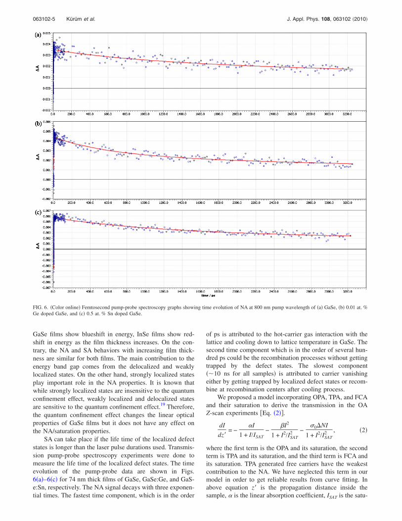
We have fitted the experimental curves to the theory bytreating ISAT and �ef f as free parameters �Figs. 3–5�. Theresults are given in Table I. ISAT values increase with increas-ing the film thickness for undoped and doped GaSe samples.In ns regime, the lowest saturation intensity threshold is1.9�10−3 GW /cm2 for 45 nm film thickness and increasesabout two orders of magnitude for 74 nm film thickness forundoped GaSe film. ISAT values also increase with increasingdoping for GaSe:Ge and GaSe:Sn films �Table I�. For thinnerfilms ISAT values are bigger for doped GaSe films than that ofundoped GaSe films as expected due to the higher density oflocalized defect states. In ps regime, the lowest saturationintensity threshold is about 9.1�10−2 GW /m2 for GaSe
TABLE I. The saturation intensity threshold ISAT and effective NA coefficients �ef f of GaSe, 0.01 at. % Gedoped GaSe, and 0.5 at. % Sn doped GaSe thin films at nanosecond and picosecond pulse durations.
MaterialThickness
�nm�
Nanosecond Picosecond
�ef f
�cm/GW�ISAT
�GW /cm2��ef f
�cm/GW�ISAT
�GW /cm2�
GaSe 45 4.4�103 1.9�10−3 5.5�102 9.1�10−2
55 6.2�103 9.6�10−3 3.5�102 4.0�10−1
65 8.2�104 5.5�10−2 1.7�104 6.7�10−1
74 3.1�105 4.5�10−1 2.5�104 8.5�10−1
GaSe:Ge 45 5.4�103 2.2�10−3 6.8�102 2.9�10−1
55 8.7�103 1.2�10−2 2.8�103 6.7�10−1
65 3.4�105 4.1�10−1 4.8�104 7.9�10−1
74 4.3�105 6.3�10−1 6.3�104 9.3�10−1
GaSe:Sn 38 9.8�103 3.2�10−3 4.8�102 1.9�10−2
45 6.8�104 6.6�10−3 3.2�103 4.2�10−1
55 3.2�105 9.1�10−2 2.9�104 8.1�10−1
65 5.5�105 6.1�10−1 7.2�104 9.3�10−1
74 7.3�105 9.4�10−1 9.0�104 1.3
063102-6 Kürüm et al. J. Appl. Phys. 108, 063102 �2010�
with 45 nm film thickness and increases about two orders ofmagnitude for 74 nm film thickness. The important key pa-rameters for a saturable absorber are its saturation intensitythreshold and its wavelength range. Our results showed thatthe saturation intensity threshold can be changed by the filmthickness and/or doping in amorphous semiconductor thinfilms. On the other hand, SA was observed at 1064 nm wave-length for nanosecond and picosecond pulse durations. TheSA behavior can be also observed at shorter and longerwavelengths since numerous localized defect states effec-tively blur the energy gap.11
�ef f values increase as the film thickness increases forboth pulse durations found from OA Z-scan experiments.�ef f values for thicker films for which saturation effect isnegligible are more reliable. Doping effect did not show anyremarkable differences in �ef f values. Since OPA is fluencedependent, the contribution of OPA to saturation is compa-rable for both nanosecond and picosecond pulse durations.�ef f contains TPA and FCA contributions to NA. TPA con-tribution is greater in ps regime, FCA contribution is greaterin ns regime. As discussed in the explanation of Fig. 3 above,high �ef f values observed for nanosecond pulse duration in-dicate that the contribution of FCA to saturation is greaterthan that of TPA. Thus, the saturation behavior takes placesat lower ISAT values for nanosecond pulse duration than pi-cosecond pulse duration.
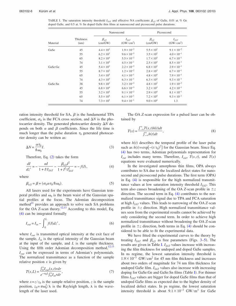
It is expected that thicker films which exhibit NA can besaturated when intensity is greater than their saturation inten-sity thresholds. In order to verify the calculated saturationintensity threshold, nanosecond and picosecond OA Z-scanexperiments were done at several input intensities above ISAT
values. The intensity dependent SA behaviors for 74 nm filmthickness of the undoped and doped GaSe films with 65 pspulse duration are shown in Fig. 7. Filling effect of the lo-calized defect states leads to SA behavior while the inputintensity increases. The intensity dependence of NA exhibitsthe similar behavior for nanosecond pulse duration.
IV. CONCLUSION
We prepared very thin �between 38–74 nm� undoped, Snand Ge doped GaSe amorphous films by thermal evaporationmethod. Energy band gap values increased with increasingfilm thickness. The energy band gap value of thicker GaSefilm is much larger than thinner GaSe film, which is mainly
due to the quantum confinement effect. The nonlinear opticalsaturation/OA behavior was investigated by OA Z-scan ex-periment for nanosecond and picosecond pulse durations. Allfilms exhibited nonlinear saturation and NA characteristicsdepending on the film thickness and/or doping due to thechange in localized defect state density. We have revealedthe mechanisms contributing the SA behavior and deter-mined saturation intensity threshold and effective NA coef-ficients. The saturation intensity thresholds increase with thefilm thickness and/or doping. The lowest saturation intensitythreshold was achieved for undoped GaSe with 45 nm filmthickness for nanosecond pulse duration. All films can besaturated at intensities higher than saturation intensity thresh-olds. We have found that nonlinear saturation intensitythreshold can be controlled not only by film thicknesses butalso by doping.
ACKNOWLEDGMENTS
This work is supported by the Research Funds of AnkaraUniversity and Turkish State of Planning Organization�DPT� under Grant No. 2003K1201903-8.
1V. Nathan, A. H. Guenther, and S. S. Mitra, J. Opt. Soc. Am. B 2, 294�1985�.
2C. C. Lee and H. Y. Fan, Phys. Rev. B 9, 3502 �1974�.3D. C. Hutchings and E. W. Van Stryland, J. Opt. Soc. Am. B 9, 2065�1992�.
4M. Sheik-Bahae, D. C. Hutchings, D. C. Hagan, and E. W. Van Stryland,IEEE J. Quantum Electron. 27, 1296 �1991�.
5M. Yüksek, A. Elmali, M. Karabulut, and G. M. Mamedov, Opt. Mater.31, 1663 �2009�.
6M. Yüksek, A. Elmali, M. Karabulut, and G. M. Mamedov, Appl. Phys. B:Lasers Opt. 98, 77 �2010�.
7J. Troles, F. Smektala, G. Boudebs, A. Monteil, B. Bureau, and J. Lucas,Opt. Mater. 25, 231 �2004�.
8F. Z. Henari, Opt. Commun. 281, 5894 �2008�.9M. Thamilselvan, K. Premnazeer, D. Mangalaraj, S. K. Narayandass, andJ. Yi, Cryst. Res. Technol. 39, 137 �2004�.
10Z. Zhao, T. Jia, J. Lin, Z. Wang, and Z. Sun, J. Phys. D: Appl. Phys. 42,045107 �2009�.
11M. Yüksek, U. Kürüm, H. G. Yaglioglu, A. Elmali, and A. Ateş, J. Appl.Phys. 107, 033115 �2010�.
12B. Gu, Y. X. Fan, J. Wang, J. Chen, J. P. Ding, H. T. Wang, and B. Guo,Phys. Rev. A 73, 065803 �2006�.
13B. Gu, Y. X. Fan, J. Chen, H.-T. Wang, J. He, and W. Ji, J. Appl. Phys.102, 083101 �2007�.
14P. A. Lee, Physics and Chemistry of Materials with Layered Crystal Struc-tures �Reidel, Dordrecht, 1976�, Vol. 4.
15V. Grasso, Electronic Structure and Electronic Transitions in Layered Ma-terials �Reidel, Dordrecht, 1986�.
FIG. 7. Intensity dependent OA Z-scan traces of undoped and doped GaSe thin films with 74 nm thickness for picosecond pulse duration: �a� GaSe, �b� 0.01at. % Ge doped GaSe, and �c� 0.5 at. % Sn doped GaSe.
063102-7 Kürüm et al. J. Appl. Phys. 108, 063102 �2010�
16M. Thamilselvan, K. Premnazeer, D. Mangalaraj, S. K. Narayandass, andJ. Yi, Physica B 337, 404 �2003�.
17M. Sheik-Bahae, A. A. Said, T. H. Wei, D. J. Hagan, and E. W. VanStryland, IEEE J. Quantum Electron. 26, 760 �1990�.
18J. I. Pankove, Optical Process in Semiconductors �Dover, New York,1971�, p. 34.
19G. Allan, C. Delerue, and M. Lannoo, Phys. Rev. Lett. 78, 3161�1997�.
20X. G. Tang, H. R. Zeng, A. L. Ding, P. S. Qiu, W. G. Luo, H. Q. Liu, andD. Mo, Solid State Commun. 116, 507 �2000�.
21G. Adomian, Solving Frontier Problems of Physics: The DecompositionMethod �Kluwer, Dordrecht, 1994�.
063102-8 Kürüm et al. J. Appl. Phys. 108, 063102 �2010�
Copyright © 2022 FDOKUMEN