Morphological manipulation of the nonlinear optical response of ZnO thin films grown by thermal...
19
This content has been downloaded from IOPscience. Please scroll down to see the full text. Download details: IP Address: 14.139.69.191 This content was downloaded on 20/11/2014 at 04:03 Please note that terms and conditions apply. Morphological manipulation of the nonlinear optical response of ZnO thin films grown by thermal evaporation View the table of contents for this issue, or go to the journal homepage for more 2014 Mater. Res. Express 1 046201 (http://iopscience.iop.org/2053-1591/1/4/046201) Home Search Collections Journals About Contact us My IOPscience
Transcript of Morphological manipulation of the nonlinear optical response of ZnO thin films grown by thermal...
This content has been downloaded from IOPscience. Please scroll down to see the full text.
Download details:
IP Address: 14.139.69.191
This content was downloaded on 20/11/2014 at 04:03
Please note that terms and conditions apply.
Morphological manipulation of the nonlinear optical response of ZnO thin films grown by
thermal evaporation
View the table of contents for this issue, or go to the journal homepage for more
2014 Mater. Res. Express 1 046201
(http://iopscience.iop.org/2053-1591/1/4/046201)
Home Search Collections Journals About Contact us My IOPscience
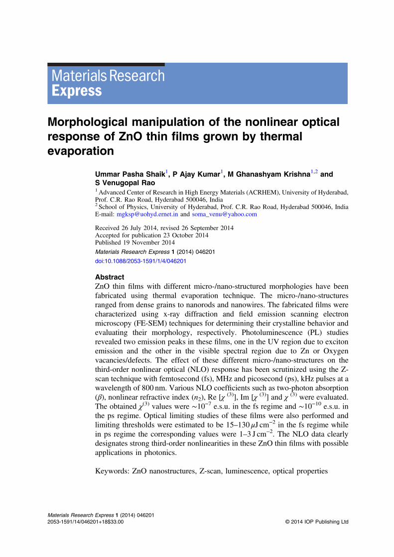
Morphological manipulation of the nonlinear opticalresponse of ZnO thin films grown by thermalevaporation
Ummar Pasha Shaik1, P Ajay Kumar1, M Ghanashyam Krishna1,2 andS Venugopal Rao1 Advanced Center of Research in High Energy Materials (ACRHEM), University of Hyderabad,Prof. C.R. Rao Road, Hyderabad 500046, India2 School of Physics, University of Hyderabad, Prof. C.R. Rao Road, Hyderabad 500046, IndiaE-mail: [email protected] and [email protected]
Received 26 July 2014, revised 26 September 2014Accepted for publication 23 October 2014Published 19 November 2014
Materials Research Express 1 (2014) 046201
doi:10.1088/2053-1591/1/4/046201
AbstractZnO thin films with different micro-/nano-structured morphologies have beenfabricated using thermal evaporation technique. The micro-/nano-structuresranged from dense grains to nanorods and nanowires. The fabricated films werecharacterized using x-ray diffraction and field emission scanning electronmicroscopy (FE-SEM) techniques for determining their crystalline behavior andevaluating their morphology, respectively. Photoluminescence (PL) studiesrevealed two emission peaks in these films, one in the UV region due to excitonemission and the other in the visible spectral region due to Zn or Oxygenvacancies/defects. The effect of these different micro-/nano-structures on thethird-order nonlinear optical (NLO) response has been scrutinized using the Z-scan technique with femtosecond (fs), MHz and picosecond (ps), kHz pulses at awavelength of 800 nm. Various NLO coefficients such as two-photon absorption(β), nonlinear refractive index (n2), Re [χ
(3)], Im [χ (3)] and χ (3) were evaluated.The obtained χ(3) values were ∼10−7 e.s.u. in the fs regime and ∼10−10 e.s.u. inthe ps regime. Optical limiting studies of these films were also performed andlimiting thresholds were estimated to be 15–130 μJ cm−2 in the fs regime whilein ps regime the corresponding values were 1–3 J cm−2. The NLO data clearlydesignates strong third-order nonlinearities in these ZnO thin films with possibleapplications in photonics.
Keywords: ZnO nanostructures, Z-scan, luminescence, optical properties
Materials Research Express 1 (2014) 0462012053-1591/14/046201+18$33.00 © 2014 IOP Publishing Ltd
1. Introduction
Zinc Oxide (ZnO) is one of the most efficient II–VI semiconductors because of its large opticalband gap, high linear refractive index and electrical properties which are responsible for avariety of applications in electronics, acousto-optic devices, photonic devices, sensors, solarcells, and optoelectronic devices [1–4]. ZnO is a direct band gap (3.37 eV) semiconductor withlarge exciton binding energy (60meV), which is much higher than that of ZnSe and GaN,leading to room temperature UV laser emission. ZnO also finds applications in UV laser diodes,and several other varieties of applications such as in exciton related photonic devices [5–8]. Theadvantage of wide band gap incorporates high-temperature/high-power operation, lower noisegeneration, higher breakdown voltages and ability to sustain large electric fields. ZnOnanowires (NWs) and nanorods in structured films have fascinating applications in nano-lasers,random lasers, biosensors, UV-LEDs, self-lighting photodynamic therapy for treatment ofcancer, and innovative nano-devices to name a few [9–15]. Optical nonlinearities insemiconductors are of particular interest due to the possibility of application in opticalswitches, optical limiters, and all-optical signal processing [16]. It has been demonstrated overthe years that nanostructuring of materials leads to significant enhancement in nonlinear optical(NLO) behavior [17]. Several groups have proposed that composite materials in thin film formwould exhibit enhanced NLO behavior [18, 19]. The higher order NLO susceptibilities areknown to be a sum of the contributions from the bulk and surface and it is well documented thatsurface roughness plays an important role in determining the NLO response of metals [20]. Zn–ZnO based composites have recently shown promise with the demonstration of enhancedemission in UV and visible region [21].
NLO properties of a variety of ZnO films and nanostructures grown using differenttechniques and growth conditions have recently been reported [7–9, 11, 22–38]. Chan et al [8]studied ZnO thin films and observed two-photon absorption (2PA, β) values of 10−6–10−7 cmW−1 in the wavelength range of 390–420 nm using 82MHz, 100 fs pulses. Han et al [9]have reported ZnO thin film data with β of 10−6–10−7 cmW−1at 790 nm using 76MHz, ∼140 fspulses. Irimpan et al [23–26] have reported NLO properties of nanostructured ZnO thin filmswith 2PA coefficients of ∼10−4–10−9 cmW−1 and χ(3) of ∼10−6–10−10 e.s.u. with ns pulses.Ouyang et al [31] studied the 2PA and optical limiting properties of graphene/ZnO compositesin organic glasses and reported a NLO coefficient (α2) of 1530 cmGW−1. Lee et al [35]synthesized ZnO nanorods with different rod diameters (50, 110, 240 nm) and investigated theirfs NLO properties and time response of the nonlinearity. However, most of the studies wereperformed using (a) single (ns/ps/fs) pulse excitation (b) MHz, fs pulse excitation and very fewof them attempted investigating exhaustive structure–property relationship. Furthermore, withfs pulses and MHz excitation one expects thermal contribution to the observed nonlinearitieswithout clear contribution of electronic nonlinearity. The objective of current work was tofabricate ZnO films with different micro-/nano-structures and investigate the NLO responsekeeping crystallographic details the same in all cases. We have performed both femtosecond (fs)NLO studies with MHz/kHz repetition rate in conjunction with picosecond (ps) NLO studieswith kHz repetition rate for all the fabricated films. It is demonstrated that the NLO response ofZnO films can be controlled by manipulating their microstructures. Our earlier studies on suchZnO films investigated the wettability, Raman, Photoluminescence (PL) properties indetail [15, 21].
2
Mater. Res. Express 1 (2014) 046201 U P Shaik et al
2. Experimental details
ZnO films were grown by thermal evaporation technique on borosilicate glass (BSG) substratesby four different annealing approaches. ZnO films were prepared by two different routes toachieve different micro-/nano-structures. In the first process, deposition of ZnO film wasachieved using zinc oxide powder as the source material followed by annealing at 150 °C in air(sample named as ZnO–film; ZnO1). The second process involved thermal oxidation of metallicZn films in air or oxygen atmosphere at 500 °C. Three different types of thermal oxidationroutes were followed: 1) annealing of Zn film at 500 °C maintaining a heating rate of 5 °Cmin−1
followed by soaking time of 30min at the same temperature (sample named as ZnO–Air; ZnO2)2), the same as 1 except the annealing is carried out in an oxygen rich atmosphere (samplenamed as ZnO–oxygen; ZnO3) 3) Zn film was rapid annealed at 500 °C in air atmosphere. i.e.,initially the furnace was heated to 500 °C at the rate of 10 °Cmin−1 and then the sample wasloaded and maintained at the same temperature for 30min followed by natural cooling innormal furnace atmosphere (sample named as ZnO4). Thicknesses of these films were measuredusing a surface profilometer (XP 100 of Ambios Technology, USA). Post annealing, thethicknesses of films were ∼250 nm, ∼980 nm, ∼670 nm and ∼1500 nm for ZnO1, ZnO2, ZnO3,and ZnO4, respectively. The crystal structures of ZnO films were characterized by a highresolution x-ray diffractometer (XRD) using Cu Kα radiation of wavelength 0.15408 nm. Theeffect of annealing routes on surface morphology was investigated by field emission scanningelectron microscopy (FE-SEM) (Carl Zeiss Model Ultra 55).
Optical absorption of the films was measured in the 200–2500 nm spectral range using aUV–vis-NIR spectrophotometer (JASCO V-570). The Raman spectra were recorded in airusing a Nd:YAG laser at 532 nm in the back scattering geometry in a CRM spectrometerequipped with a confocal microscope and 100X objective with a CCD detector (model alpha300 of WiTec, Germany). The PL spectra were recorded in air in the same spectrometer using a355 nm diode laser with ∼7mW input power in reflection configuration and 40X UV objectiveswith a CCD detector (WiTec, Germany). NLO characterization was accomplished using thestandard Z-scan technique [39]. In the fs regime, a Ti: sapphire oscillator (Chameleon Ultra II,Coherent) producing ∼140 fs pulses with a repetition 80MHz at 800 nm was used. The samplewas scanned along the Z-direction through the focus of a 100mm focal length lens. The inputbeam was spatially filtered to obtain a pure Gaussian profile in the far field. The sample wasplaced on a 10 μm resolution translation stage and data was collected manually using thedetector (Field-Max). The transmitted intensity was recorded as a function of the sampleposition. The beam waist (ωo) estimated at the focus was ∼25 μm with a correspondingRayleigh range of ∼2.54mm. In the ps regime, studies were performed by using Ti: sapphireamplifier delivering ∼2 ps, 1 kHz pulses at 800 nm. The amplifier was seeded with ∼15 fs pulsesfrom an oscillator (MICRA, Coherent, 1W, 80MHz, 800 nm). The average power fromamplifier was ∼2W. The laser beam was focused by a 200mm focal length lens. The outputtransmittance was recorded by using a photodiode in combination with a lock-in amplifier.Complete details of the ps experiments have been reported in our earlier works [40–43]. TheNLO studies were performed on all the samples with linear transmittance of ∼60–75% at800 nm. All the closed aperture scans were performed at lower peak intensities so as to avoidany contribution from higher order nonlinear effects (the value of Δϕ estimated in all the caseswas <π). The experiments were repeated more than once and the average nonlinear opticalcoefficients were retrieved from the theoretical fits to experimental data.
3
Mater. Res. Express 1 (2014) 046201 U P Shaik et al
3. Results and discussion
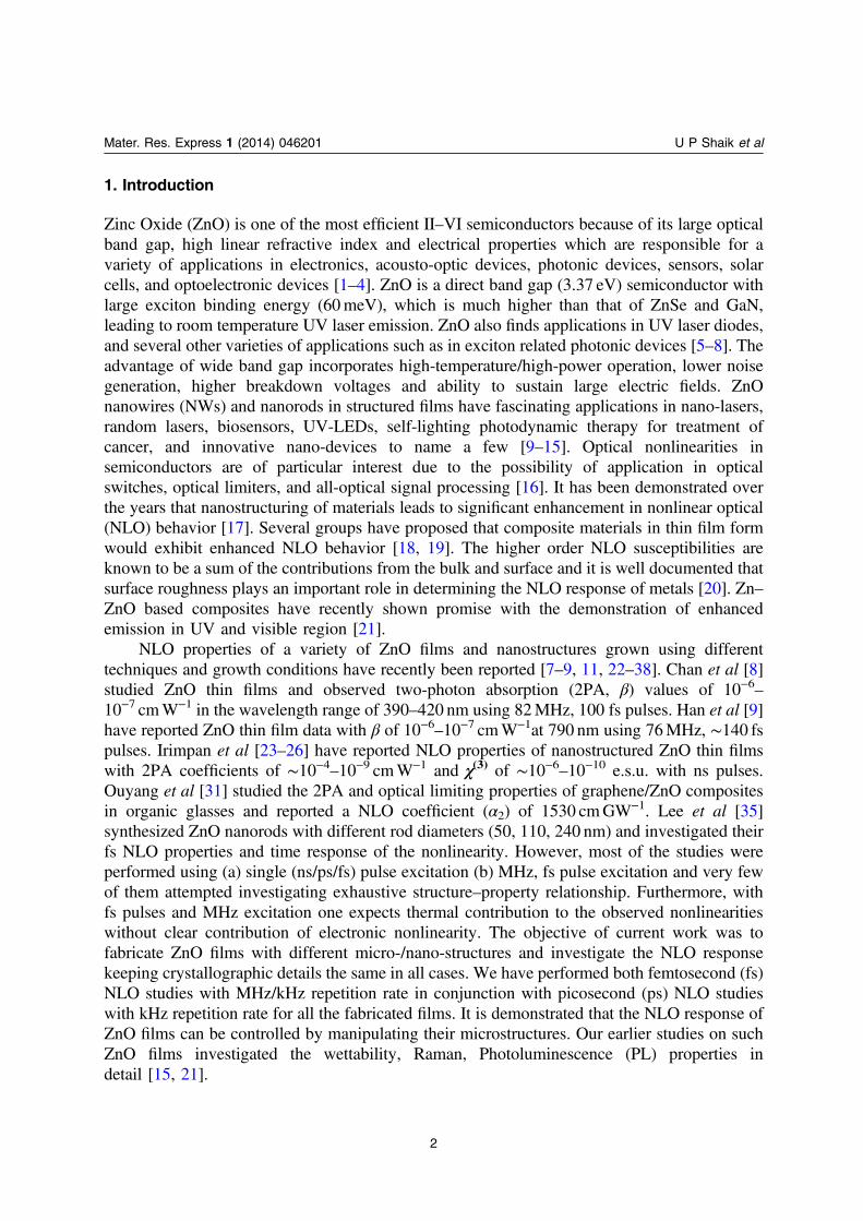
The XRD data of ZnO1, ZnO2, ZnO3, and ZnO4 are shown in figure 1. The diffraction peaks ofall samples exactly coincided with that of hexagonal ZnO structure and the peaks were indexedaccording to JCPDS No. 89-1397. We did not observe any significant Zn residue from the XRDpatterns of ZnO2, ZnO3 and ZnO4 [figures 1(b)–(d)], which confirmed that there was acomplete phase transition from hexagonal Zn (as deposited) to hexagonal ZnO at 500 °Cannealing temperature [15].
The hexagonal ZnO unit cell parameters were calculated from the XRD patterns and wereindependent of oxidation history of the samples. The calculated unit cell parameters were,a= 3.2 ± 0.2Å and c = 5.2 ± 0.2Å. The average crystallite sizes were calculated from FHWM ofZnO peaks using Scherrer’s formula [44] and the obtained value was 36 ± 2 nm for the threefilms of ZnO2, ZnO3, and ZnO4 and independent of different oxidation approaches used.However, ZnO1 had a crystallite size of 8 ± 2 nm. The lower value of the crystallite size in thecase of ZnO1 can be attributed to the lower annealing temperature as well as the lower thicknessof this film.
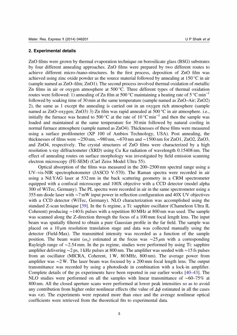
The morphology of ZnO1 is displayed in figure 2(a). The SEM data revealed a densemicrostructure with flakes emerging out of the surface. Closer examination revealed that therewere pores in the film which were randomly distributed. Morphology of ZnO2 (depicted infigure 2(b)) also resulted in dense microstructure but there was evidence for formation ofaggregates on the surface which rendered the surface rough. The microstructure of ZnO3 (datapresented in figure 2(c)) depicts formation of micro/nanorods that grew along the plane of thefilm surface. However, the most drastic change occurred in the microstructure of ZnO4, shownin figure 2(d). There was transformation into nanowires with diameters of ∼15–100 nm andlengths extending to a few μm emerging from the film surface. From the high resolution imagespresented in figures 2(e)–(h) it is evident that the annealing route had a significant effect on thesurface morphology of ZnO films. The microstructures ranged from dense films to slightlyporous microstructures, micro/nano rods and nanowires. Hence, these samples provided goodexamples for investigating the effect of differing microstructures on NLO properties of resultingZnO surfaces.
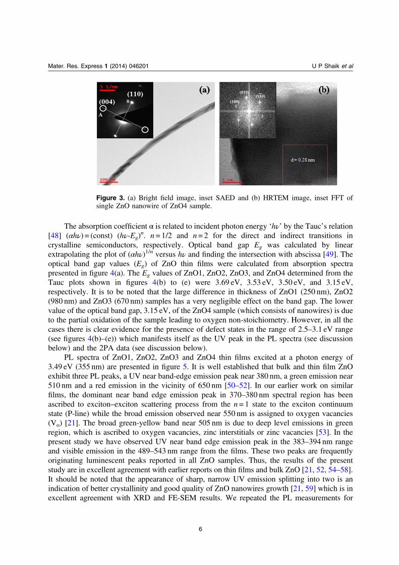
To know the growth direction of obtained ZnO nanowires, ZnO4 sample was examinedunder TEM. Figure 3(a) shows the bright field TEM image of ZnO nanowire selected from
Figure 1. XRD pattern of thin films of (a) ZnO1 (b) ZnO2 (c) ZnO3 and (d) ZnO4.
4
Mater. Res. Express 1 (2014) 046201 U P Shaik et al
ZnO4 sample. The bright field image shows the nanowire of diameter 30 nm and length 800 nm.Selected area electron diffraction (SAED) pattern of the ZnO nanowire shows that the Wurtzitestructure of ZnO was formed (inset of figure 3(a)). Figure 3(b) shows the HRTEM image of thesame single ZnO nanowire presented in the bright field image of figure 3(a). From the fastFourier transform (FFT) (inset of figure 3(b)) analysis of the high resolution TEM (HRTEM)images, the d spacing between lattice planes was calculated as 0.28 nm, indicating that the ZnOnanowires were grown in [1 0 −1 0] direction. Our results are in good agreement with theprevious reported results [45–47].
Figure 2. FE-SEM images of (a), (e) ZnO1 (b), (f) ZnO2 (c), (g) ZnO3 (d), (h) ZnO4.(a)-(d) are in 1 μm scale and (e)-(h) are in 200 nm scale.
5
Mater. Res. Express 1 (2014) 046201 U P Shaik et al
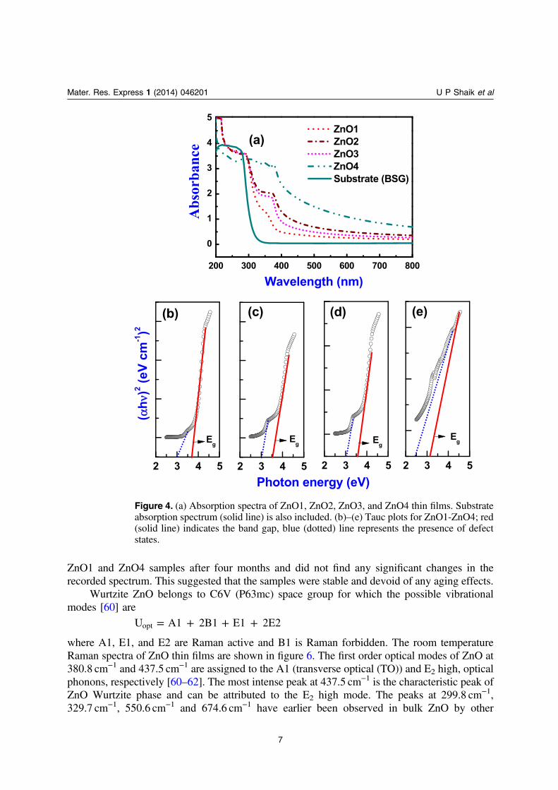
The absorption coefficient α is related to incident photon energy ‘hν’ by the Tauc’s relation[48] (αhν) = (const) (hν-Eg)
n. n= 1/2 and n= 2 for the direct and indirect transitions incrystalline semiconductors, respectively. Optical band gap Eg was calculated by linearextrapolating the plot of (αhν)1/n versus hν and finding the intersection with abscissa [49]. Theoptical band gap values (Eg) of ZnO thin films were calculated from absorption spectrapresented in figure 4(a). The Eg values of ZnO1, ZnO2, ZnO3, and ZnO4 determined from theTauc plots shown in figures 4(b) to (e) were 3.69 eV, 3.53 eV, 3.50 eV, and 3.15 eV,respectively. It is to be noted that the large difference in thickness of ZnO1 (250 nm), ZnO2(980 nm) and ZnO3 (670 nm) samples has a very negligible effect on the band gap. The lowervalue of the optical band gap, 3.15 eV, of the ZnO4 sample (which consists of nanowires) is dueto the partial oxidation of the sample leading to oxygen non-stoichiometry. However, in all thecases there is clear evidence for the presence of defect states in the range of 2.5–3.1 eV range(see figures 4(b)–(e)) which manifests itself as the UV peak in the PL spectra (see discussionbelow) and the 2PA data (see discussion below).
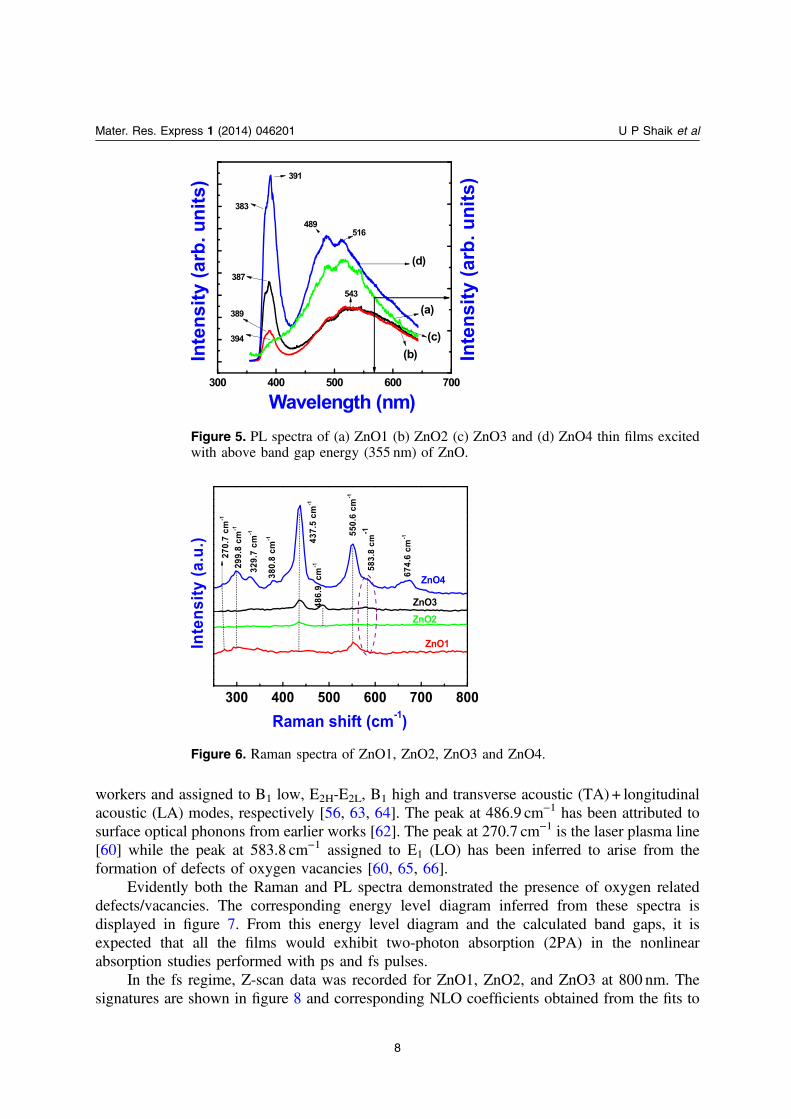
PL spectra of ZnO1, ZnO2, ZnO3 and ZnO4 thin films excited at a photon energy of3.49 eV (355 nm) are presented in figure 5. It is well established that bulk and thin film ZnOexhibit three PL peaks, a UV near band-edge emission peak near 380 nm, a green emission near510 nm and a red emission in the vicinity of 650 nm [50–52]. In our earlier work on similarfilms, the dominant near band edge emission peak in 370–380 nm spectral region has beenascribed to exciton–exciton scattering process from the n = 1 state to the exciton continuumstate (P-line) while the broad emission observed near 550 nm is assigned to oxygen vacancies(Vo) [21]. The broad green-yellow band near 505 nm is due to deep level emissions in greenregion, which is ascribed to oxygen vacancies, zinc interstitials or zinc vacancies [53]. In thepresent study we have observed UV near band edge emission peak in the 383–394 nm rangeand visible emission in the 489–543 nm range from the films. These two peaks are frequentlyoriginating luminescent peaks reported in all ZnO samples. Thus, the results of the presentstudy are in excellent agreement with earlier reports on thin films and bulk ZnO [21, 52, 54–58].It should be noted that the appearance of sharp, narrow UV emission splitting into two is anindication of better crystallinity and good quality of ZnO nanowires growth [21, 59] which is inexcellent agreement with XRD and FE-SEM results. We repeated the PL measurements for
Figure 3. (a) Bright field image, inset SAED and (b) HRTEM image, inset FFT ofsingle ZnO nanowire of ZnO4 sample.
6
Mater. Res. Express 1 (2014) 046201 U P Shaik et al
ZnO1 and ZnO4 samples after four months and did not find any significant changes in therecorded spectrum. This suggested that the samples were stable and devoid of any aging effects.
Wurtzite ZnO belongs to C6V (P63mc) space group for which the possible vibrationalmodes [60] are
= + + +U A1 2B1 E1 2E2opt
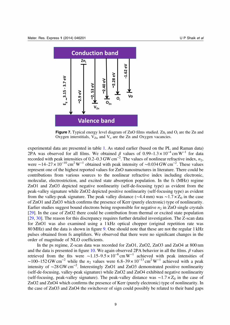
where A1, E1, and E2 are Raman active and B1 is Raman forbidden. The room temperatureRaman spectra of ZnO thin films are shown in figure 6. The first order optical modes of ZnO at380.8 cm−1 and 437.5 cm−1 are assigned to the A1 (transverse optical (TO)) and E2 high, opticalphonons, respectively [60–62]. The most intense peak at 437.5 cm−1 is the characteristic peak ofZnO Wurtzite phase and can be attributed to the E2 high mode. The peaks at 299.8 cm−1,329.7 cm−1, 550.6 cm−1 and 674.6 cm−1 have earlier been observed in bulk ZnO by other
Figure 4. (a) Absorption spectra of ZnO1, ZnO2, ZnO3, and ZnO4 thin films. Substrateabsorption spectrum (solid line) is also included. (b)–(e) Tauc plots for ZnO1-ZnO4; red(solid line) indicates the band gap, blue (dotted) line represents the presence of defectstates.
7
Mater. Res. Express 1 (2014) 046201 U P Shaik et al
workers and assigned to B1 low, E2H-E2L, B1 high and transverse acoustic (TA) + longitudinalacoustic (LA) modes, respectively [56, 63, 64]. The peak at 486.9 cm−1 has been attributed tosurface optical phonons from earlier works [62]. The peak at 270.7 cm−1 is the laser plasma line[60] while the peak at 583.8 cm−1 assigned to E1 (LO) has been inferred to arise from theformation of defects of oxygen vacancies [60, 65, 66].
Evidently both the Raman and PL spectra demonstrated the presence of oxygen relateddefects/vacancies. The corresponding energy level diagram inferred from these spectra isdisplayed in figure 7. From this energy level diagram and the calculated band gaps, it isexpected that all the films would exhibit two-photon absorption (2PA) in the nonlinearabsorption studies performed with ps and fs pulses.
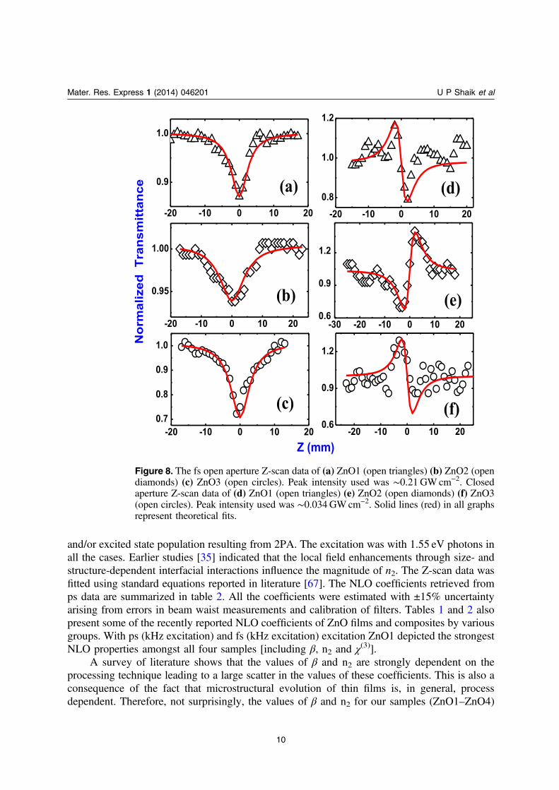
In the fs regime, Z-scan data was recorded for ZnO1, ZnO2, and ZnO3 at 800 nm. Thesignatures are shown in figure 8 and corresponding NLO coefficients obtained from the fits to
Figure 5. PL spectra of (a) ZnO1 (b) ZnO2 (c) ZnO3 and (d) ZnO4 thin films excitedwith above band gap energy (355 nm) of ZnO.
Figure 6. Raman spectra of ZnO1, ZnO2, ZnO3 and ZnO4.
8
Mater. Res. Express 1 (2014) 046201 U P Shaik et al
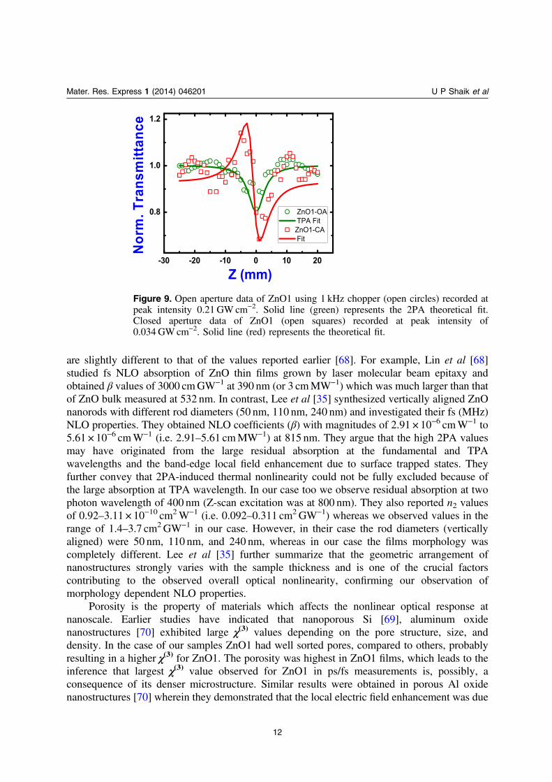
experimental data are presented in table 1. As stated earlier (based on the PL and Raman data)2PA was observed for all films. We obtained β values of 0.99–1.3 × 10⁻⁴ cmW−1 for datarecorded with peak intensities of 0.2–0.3GWcm−2. The values of nonlinear refractive index, n2,were ∼14–27 × 10−10 cm2W−1 obtained with peak intensity of ∼0.034GWcm−2. These valuesrepresent one of the highest reported values for ZnO nanostructures in literature. There could becontributions from various sources to the nonlinear refractive index including electronic,molecular, electrostriction, and excited state absorption population. In the fs (MHz) regimeZnO1 and ZnO3 depicted negative nonlinearity (self-de-focusing type) as evident from thepeak-valley signature while ZnO2 depicted positive nonlinearity (self-focusing type) as evidentfrom the valley-peak signature. The peak valley distance (∼4.4mm) was ∼1.7 ×Z0 in the caseof ZnO1 and ZnO3 which confirms the presence of Kerr (purely electronic) type of nonlinearity.Earlier studies suggest bound electrons being responsible for negative n2 in ZnO single crystals[29]. In the case of ZnO2 there could be contribution from thermal or excited state population[29, 30]. The reason for this discrepancy requires further detailed investigation. The Z-scan datafor ZnO1 was also examined using a 1 kHz optical chopper (original repetition rate was80MHz) and the data is shown in figure 9. One should note that these are not the regular 1 kHzpulses obtained from fs amplifiers. We observed that there were no significant changes in theorder of magnitude of NLO coefficients.
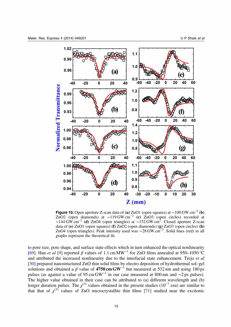
In the ps regime, Z-scan data was recorded for ZnO1, ZnO2, ZnO3 and ZnO4 at 800 nmand the data is presented in figure 10. We again observed 2PA behavior in all the films. β valuesretrieved from the fits were ∼1.15–9.5 × 10⁻⁸ cmW−1 achieved with peak intensities of∼100–152GWcm−2 while the n2 values were 6.8–39 × 10−13 cm2W−1 achieved with a peakintensity of ∼28GWcm−2. Interestingly ZnO1 and ZnO3 demonstrated positive nonlinearity(self-de-focusing, valley-peak signature) while ZnO2 and ZnO4 exhibited negative nonlinearity(self-focusing, peak-valley signature). The peak-valley distance was ∼1.7 × Z0 in the case ofZnO2 and ZnO4 which confirms the presence of Kerr (purely electronic) type of nonlinearity. Inthe case of ZnO3 and ZnO4 the switchover of sign could possibly be related to their band gaps
Figure 7. Typical energy level diagram of ZnO films studied. Zni and Oi are the Zn andOxygen interstitials, VZn and Vo are the Zn and Oxygen vacancies.
9
Mater. Res. Express 1 (2014) 046201 U P Shaik et al
and/or excited state population resulting from 2PA. The excitation was with 1.55 eV photons inall the cases. Earlier studies [35] indicated that the local field enhancements through size- andstructure-dependent interfacial interactions influence the magnitude of n2. The Z-scan data wasfitted using standard equations reported in literature [67]. The NLO coefficients retrieved fromps data are summarized in table 2. All the coefficients were estimated with ±15% uncertaintyarising from errors in beam waist measurements and calibration of filters. Tables 1 and 2 alsopresent some of the recently reported NLO coefficients of ZnO films and composites by variousgroups. With ps (kHz excitation) and fs (kHz excitation) excitation ZnO1 depicted the strongestNLO properties amongst all four samples [including β, n2 and χ(3)].
A survey of literature shows that the values of β and n2 are strongly dependent on theprocessing technique leading to a large scatter in the values of these coefficients. This is also aconsequence of the fact that microstructural evolution of thin films is, in general, processdependent. Therefore, not surprisingly, the values of β and n2 for our samples (ZnO1–ZnO4)
Figure 8. The fs open aperture Z-scan data of (a) ZnO1 (open triangles) (b) ZnO2 (opendiamonds) (c) ZnO3 (open circles). Peak intensity used was ∼0.21 GW cm−2. Closedaperture Z-scan data of (d) ZnO1 (open triangles) (e) ZnO2 (open diamonds) (f) ZnO3(open circles). Peak intensity used was ∼0.034 GW cm−2. Solid lines (red) in all graphsrepresent theoretical fits.
10
Mater. Res. Express 1 (2014) 046201 U P Shaik et al
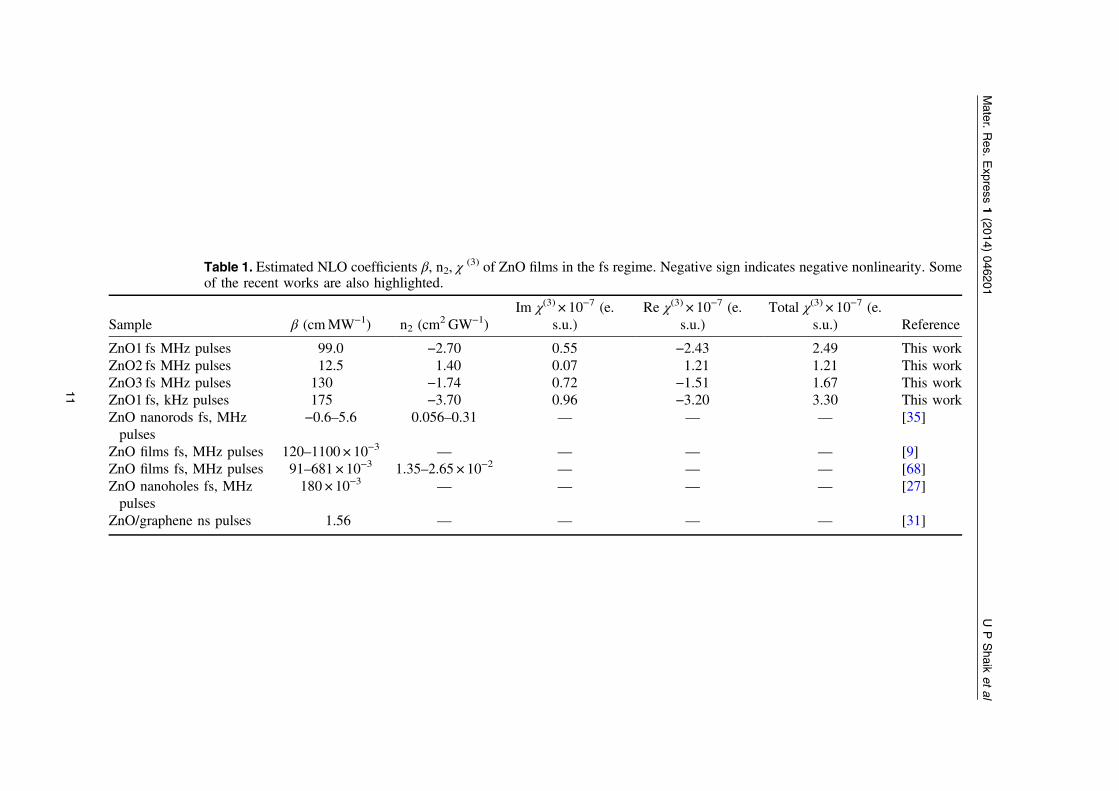
Table 1. Estimated NLO coefficients β, n2, χ(3) of ZnO films in the fs regime. Negative sign indicates negative nonlinearity. Some
of the recent works are also highlighted.
Sample β (cmMW−1) n2 (cm2 GW−1)
Im χ(3) × 10−7 (e.s.u.)
Re χ(3) × 10−7 (e.s.u.)
Total χ(3) × 10−7 (e.s.u.) Reference
ZnO1 fs MHz pulses 99.0 −2.70 0.55 −2.43 2.49 This workZnO2 fs MHz pulses 12.5 1.40 0.07 1.21 1.21 This workZnO3 fs MHz pulses 130 −1.74 0.72 −1.51 1.67 This workZnO1 fs, kHz pulses 175 −3.70 0.96 −3.20 3.30 This workZnO nanorods fs, MHzpulses
−0.6–5.6 0.056–0.31 — — — [35]
ZnO films fs, MHz pulses 120–1100 × 10−3 — — — — [9]ZnO films fs, MHz pulses 91–681 × 10−3 1.35–2.65 × 10⁻² — — — [68]ZnO nanoholes fs, MHzpulses
180 × 10−3 — — — — [27]
ZnO/graphene ns pulses 1.56 — — — — [31]
11
Mater.
Res.
Express
1(2014)
046201U
PShaik
etal
are slightly different to that of the values reported earlier [68]. For example, Lin et al [68]studied fs NLO absorption of ZnO thin films grown by laser molecular beam epitaxy andobtained β values of 3000 cmGW−1 at 390 nm (or 3 cmMW−1) which was much larger than thatof ZnO bulk measured at 532 nm. In contrast, Lee et al [35] synthesized vertically aligned ZnOnanorods with different rod diameters (50 nm, 110 nm, 240 nm) and investigated their fs (MHz)NLO properties. They obtained NLO coefficients (β) with magnitudes of 2.91 × 10⁻⁶ cmW−1 to5.61 × 10−6 cmW−1 (i.e. 2.91–5.61 cmMW−1) at 815 nm. They argue that the high 2PA valuesmay have originated from the large residual absorption at the fundamental and TPAwavelengths and the band-edge local field enhancement due to surface trapped states. Theyfurther convey that 2PA-induced thermal nonlinearity could not be fully excluded because ofthe large absorption at TPA wavelength. In our case too we observe residual absorption at twophoton wavelength of 400 nm (Z-scan excitation was at 800 nm). They also reported n2 valuesof 0.92–3.11 × 10⁻¹⁰ cm2W−1 (i.e. 0.092–0.311 cm2GW−1) whereas we observed values in therange of 1.4–3.7 cm2GW−1 in our case. However, in their case the rod diameters (verticallyaligned) were 50 nm, 110 nm, and 240 nm, whereas in our case the films morphology wascompletely different. Lee et al [35] further summarize that the geometric arrangement ofnanostructures strongly varies with the sample thickness and is one of the crucial factorscontributing to the observed overall optical nonlinearity, confirming our observation ofmorphology dependent NLO properties.
Porosity is the property of materials which affects the nonlinear optical response atnanoscale. Earlier studies have indicated that nanoporous Si [69], aluminum oxidenanostructures [70] exhibited large χ(3) values depending on the pore structure, size, anddensity. In the case of our samples ZnO1 had well sorted pores, compared to others, probablyresulting in a higher χ(3) for ZnO1. The porosity was highest in ZnO1 films, which leads to theinference that largest χ(3) value observed for ZnO1 in ps/fs measurements is, possibly, aconsequence of its denser microstructure. Similar results were obtained in porous Al oxidenanostructures [70] wherein they demonstrated that the local electric field enhancement was due
Figure 9. Open aperture data of ZnO1 using 1 kHz chopper (open circles) recorded atpeak intensity 0.21 GW cm−2. Solid line (green) represents the 2PA theoretical fit.Closed aperture data of ZnO1 (open squares) recorded at peak intensity of0.034 GW cm−2. Solid line (red) represents the theoretical fit.
12
Mater. Res. Express 1 (2014) 046201 U P Shaik et al
to pore size, pore shape, and surface state effects which in turn enhanced the optical nonlinearity[69]. Han et al [9] reported β values of 1.1 cmMW−1 for ZnO films annealed at 950–1050 °Cand attributed the increased nonlinearity due to the interfacial state enhancement. Trejo et al[30] prepared nanostructured ZnO thin solid films by electro deposition of hydrothermal sol–gelsolutions and obtained a β value of 4750 cmGW−1 but measured at 532 nm and using 180 pspulses (as against a value of 95 cmGW−1 in our case measured at 800 nm and ∼2 ps pulses).The higher value obtained in their case can be attributed to (a) different wavelength and (b)longer duration pulses. The χ(3) values obtained in the present studies (10−7 esu) are similar tothat that of χ(3) values of ZnO microcrystallite thin films [71] studied near the excitonic
Figure 10. Open aperture Z-scan data of (a) ZnO1 (open squares) at ∼100GWcm−2 (b)ZnO2 (open diamonds) at ∼119GWcm−2 (c) ZnO3 (open circles) recorded at∼144 GWcm−2 (d) ZnO4 (open triangles) at ∼152GW cm2. Closed aperture Z-scandata of (e) ZnO1 (open squares) (f) ZnO2 (open diamonds) (g) ZnO3 (open circles) (h)ZnO4 (open triangles). Peak intensity used was ∼28 GWcm−2. Solid lines (red) in allgraphs represent the theoretical fit.
13
Mater. Res. Express 1 (2014) 046201 U P Shaik et al
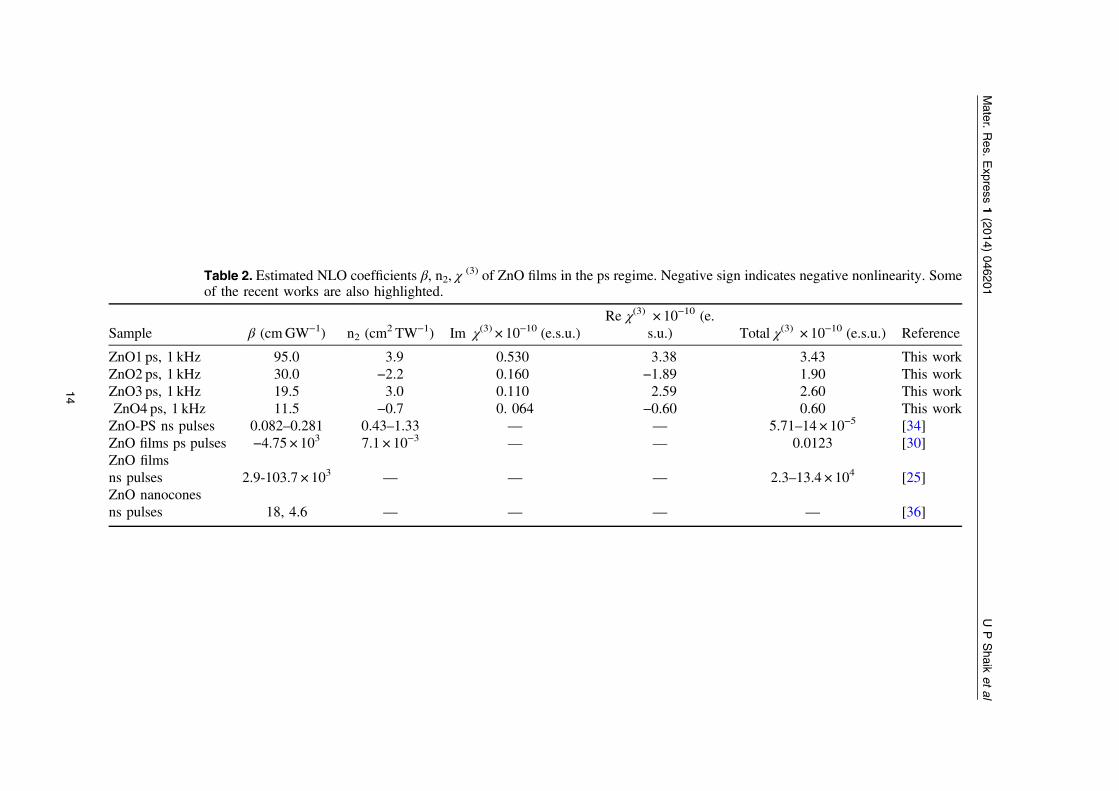
Table 2. Estimated NLO coefficients β, n2, χ(3) of ZnO films in the ps regime. Negative sign indicates negative nonlinearity. Some
of the recent works are also highlighted.
Sample β (cmGW−1) n2 (cm2 TW−1) Im χ(3) × 10−10 (e.s.u.)
Re χ(3) × 10−10 (e.s.u.) Total χ(3) × 10−10 (e.s.u.) Reference
ZnO1 ps, 1 kHz 95.0 3.9 0.530 3.38 3.43 This workZnO2 ps, 1 kHz 30.0 −2.2 0.160 −1.89 1.90 This workZnO3 ps, 1 kHz 19.5 3.0 0.110 2.59 2.60 This workZnO4 ps, 1 kHz 11.5 −0.7 0. 064 −0.60 0.60 This workZnO-PS ns pulses 0.082–0.281 0.43–1.33 — — 5.71–14 × 10−5 [34]ZnO films ps pulses −4.75 × 10³ 7.1 × 10⁻³ — — 0.0123 [30]ZnO filmsns pulses 2.9-103.7 × 10³ — — — 2.3–13.4 × 10⁴ [25]ZnO nanoconesns pulses 18, 4.6 — — — — [36]
14
Mater.
Res.
Express
1(2014)
046201U
PShaik
etal
resonance at various temperatures using fs (MHz pulses) degenerate four-wave-mixingtechnique. Further detailed studies are necessary to exactly identify the mechanism for superiornonlinearities in our case. The values of β and n2 for pure ZnO thin films measured with fs MHzpulse excitation were ∼10−6 cmW−1 and ∼10−11 cm2W−1, respectively [35]. The values of βand n2 for bulk ZnO measured using 25 ps, 532 nm excitation were found to be ∼4.2 cmGW−1
and ∼9 × 10⁻¹⁵ cm2W−1, respectively [28, 29]. The NLO coefficients β and n2 of NLO crystalssuch as KDP and BBO are ∼0.9 cmGW−1 and 5–6 × 10⁻¹⁶ cm2W−1 [72, 73].
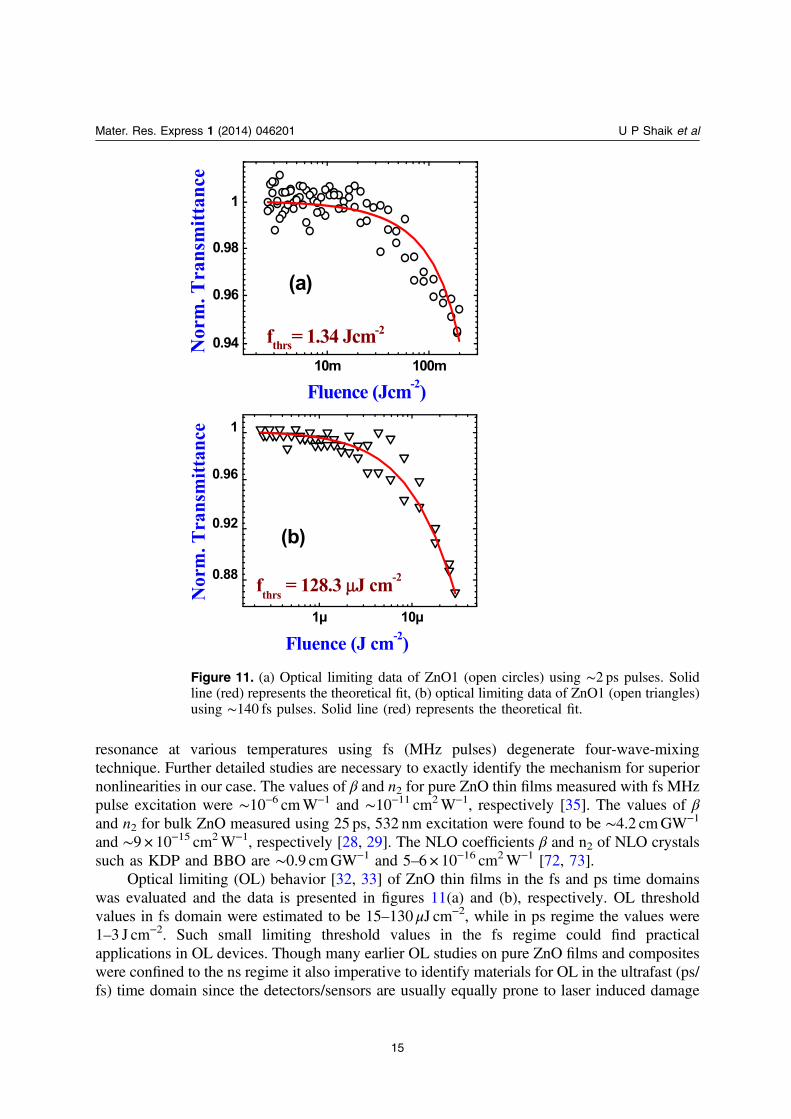
Optical limiting (OL) behavior [32, 33] of ZnO thin films in the fs and ps time domainswas evaluated and the data is presented in figures 11(a) and (b), respectively. OL thresholdvalues in fs domain were estimated to be 15–130 μJ cm−2, while in ps regime the values were1–3 J cm−2. Such small limiting threshold values in the fs regime could find practicalapplications in OL devices. Though many earlier OL studies on pure ZnO films and compositeswere confined to the ns regime it also imperative to identify materials for OL in the ultrafast (ps/fs) time domain since the detectors/sensors are usually equally prone to laser induced damage
Figure 11. (a) Optical limiting data of ZnO1 (open circles) using ∼2 ps pulses. Solidline (red) represents the theoretical fit, (b) optical limiting data of ZnO1 (open triangles)using ∼140 fs pulses. Solid line (red) represents the theoretical fit.
15
Mater. Res. Express 1 (2014) 046201 U P Shaik et al
with those pulses associated with large peak intensities. In the fs case the threshold for OL waslower since the magnitude of nonlinearities was large due to thermal contribution. In the psregime the measurements were performed with kHz pulses and, therefore, the thermalcontribution could be negligible.
We have also evaluated the contribution of thermal effects [68] for data recorded withMHz repetition rate. Thermo-optical nonlinearity is an important parameter while calculatingthe nonlinear index of refraction. In particular, thermo-optic contribution is added by non-localnonlinearity while using ultra short laser pulses. For some materials this contribution becomessignificant. It depends on the thermal characteristic time and thermo-optic coefficient. In the firstcase contribution is significant, if thermal characteristic time τc is longer than the time period ofthe laser. Thermal characteristic time τc was calculated using the parameters of beam waist (ωo),density (ρ), specific heat (cp), and thermal conductivity (k) [68]
τω ρ
=c
k4. (1)
o pc
2
The estimated τc was ∼8.3 × 10⁻⁶ s for the fs data. The thermo-optic coefficient values forZnO1, ZnO2, and ZnO3 in the fs regime were calculated using the relation
Δαρ
=nF
c
n
T2dd
. (2)v
00
F0 is the fluence, ρ is the density, cv is the specific heat, and 1
2denotes the fluence averaging
factor. Thermo-optic coefficient ⎡⎣ ⎤⎦n
T
d
dvalues estimated were (a) ZnO1: 2.14 × 10⁻⁴ K−1 (b)
ZnO2: 2.41 × 10⁻⁴ K−1 (c) ZnO3: 2.01 × 10⁻⁴ K−1. In the ps regime we performed themeasurements with 1 kHz pulses (1ms time between consecutive pulses) and, therefore, weexpect minimal thermal contributions to the observed nonlinearity and it predominantly haselectronic contributions.
Our future studies will focus on (a) recording the spectral dependence of the nonlinearitiesin the ps regime, (b) understanding the excited state dynamics in these thin films using ps/fsdegenerate and non-degenerate pump-probe studies [40, 74, 75] and (c) estimating the figures ofmerit for NLO application over the entire visible spectral range using ps/fs kHz pulses.
4. Conclusions
NLO characterization in the fs and ps regimes has been performed on ZnO thin films fabricatedwith different morphologies. The micro-/nano-structures were characterized using XRD(crystalline behavior) and FE-SEM (morphology). All the films exhibited 2PA at 800 nm inboth the regimes with magnitudes of ∼10−4 cmW−1, ∼10−8 cmW−1 in fs, ps regimes,respectively. The n2 values were ∼10−9 cm2W−1 in ps and ∼10−12 cm2W−1 in fs regimes. Thirdorder nonlinearity [χ(3)] values were also estimated. Very low limiting threshold values(15–130 μJ cm−2) were recorded with fs pulses. It is demonstrated that NLO response of ZnOfilms can be controlled by manipulating their microstructures.
16
Mater. Res. Express 1 (2014) 046201 U P Shaik et al
Acknowledgments
SVR acknowledges the financial support from DRDO. PAK acknowledges the support of MrKrishna Podagatlapalli and Mr Syed Hamad during NLO studies. UPS acknowledges support ofDr M A Mohiddon during PL, Raman measurements.
References
[1] Yan R, Gargas D and Yang P 2009 Nat. Photon. 3 569[2] Özgür Ü, Alivov Y I, Liu C, Teke A, Reshchikov M A, Doğan S, Avrutin V, Cho S-J and Morkoç H 2005
J. Appl. Phys. 98 041301[3] Panda D and Tseng T-Y 2013 J. Mater. Sci. 48 6849[4] Dhara S and Giri P K 2013 Rev. Nanosci. Nanotechnol. 2 1[5] Ou P-C, Lin J-H, Chang C-A, Liu W-R and Hsieh W-F 2010 J. Phys. D: Appl. Phys. 43 495103[6] Tang Z K, Wong G K L, Yu P, Kawasaki M and Ohtomo A 1998 Appl. Phys. Lett. 72 3270[7] Das S K, Biswas M, Byrne D, Bock M, McGlynn E, Breusing M and Grunwald R 2010 J. Appl. Phys. 108
043107[8] Chan Y-P, Lin J-H, Hsu C-C and Hsieh W-F 2008 Opt. Express 16 19900[9] Han Y B, Han J B, Ding S, Chen D J and Wang Q Q 2005 Opt. Express 13 9211
[10] Gurav K V et al 2014 Sensors Actuators B 190 439[11] Nagaraja K K, Pramodini S, Poornesh P and Nagaraja H S 2013 J. Phys. D: Appl. Phys. 46 055106[12] Thareja R K and Mitra A 2000 Appl. Phys. B 71 181[13] Ou P-C, Liu W-R, Ton H-J, Lin J-H and Hsieh W-F 2011 J. Appl. Phys. 109 013102[14] Wang K, Zhou J, Yuan L, Tao Y, Chen J, Lu P and Wang Z L 2012 Nano. Lett. 12 833[15] Shaik U P, Kshirsagar S, Krishna M G, Tewari S P, Purkayastha D D and Madhurima V 2012 Mater. Lett.
75 51[16] Fainman Y, Ma J and Lee S H 1993 Mater. Sci. Rep. 9 53[17] Ray P C 2010 Chem. Rev. 110 5332[18] Boyd R W, Gehr R J, Fischer G L and Sipe J E 1996 Pure Appl. Opt. 5 505[19] Beecroft L L and Ober C K 1997 Chem. Mater. 9 1302[20] Poliakov E Y, Markel V A and Shalaev V M 1998 Phys. Rev. B 57 14901[21] Kshirsagar S, Shaik U P, Krishna M G and Tewari S P 2013 J. Lumin. 136 26[22] Johnson J C, Yan H, Schaller R D, Petersen P B, Yang P and Saykally R J 2002 Nano. Lett. 2 279[23] Irimpan L, Deepthy A, Krishnan B, Kukreja L M, Nampoori V P N and Radhakrishnan P 2008 Opt.
Commun. 281 2938[24] Irimpan L, Deepthy A, Krishnan B, Kukreja L M, Nampoori V P N and Radhakrishnan P 2008 Appl. Phys. B
90 547[25] Irimpan L, Nampoori V P N, Radhakrishnan P, Krishnan B and Deepthy A 2008 J. Appl. Phys. 103 033118[26] Irimpan L, Ambika D, Kumar V, Nampoori V P N and Radhakrishnan P 2008 J. Appl. Phys. 104 033105[27] Zhang L-C, Yang G, Wang K, Fu M, Wang Y, Long H and Lu P-X 2013 Opt. Commun. 291 395[28] Zhang X J, Ji W and Tang S H 1997 J. Opt. Soc. Am. B 14 1951[29] Zhang X, Fang H, Tang S and Ji W 1997 Appl. Phys. B 65 549[30] Trejo-Valdez M, Torres C T-, Chacon J H C-, Armenta G A G-, Gil C I G- and Khomenko A V 2013 Opt.
Laser Technol. 49 75[31] Ouyang Q-Y, Xu Z, Lei Z, Dong H, Yu H, Qi L, Li C and Chen Y 2014 Carbon 67 214[32] Jamal R K, Suhail A M, Hussein M T and Kbashi H J 2012 Int. J. Thin Film Sci. Technol. 1 61[33] Haripadmam P C, Kavitha M K, John H, Krishnan B and Gopinath P 2012 Appl. Phys. Lett. 101 071103[34] Jeeju P P, Jayalaxmi S, Chandrasekharan K and Sudheesh P 2012 Opt. Commun. 285 5433
17
Mater. Res. Express 1 (2014) 046201 U P Shaik et al
[35] Lee H W, Lee K M, Lee S, Koh K H, Park J-Y, Kim K and Rotermund F 2007 Chem. Phys. Lett. 447 86[36] Haripadmam P C, John H, Philip R and Gopinath P 2014 Opt. Lett. 39 474[37] Vinodkumar R, Lethy K J, Arunkumar P R, Krishnan R R, Pillai N V, Pillai V P M and Philip R 2010 Mater.
Chem. Phys. 121 406[38] Prakash G V, Pradeesh K, Kumar A, Kumar R, Rao S V, Markham M L and Baumberg J J 2008 Mater. Lett.
62 1183[39] Bahae M S, Said A A, Wel T H, Hagen D J and Van Stryland E W 1990 IEEE J. Quant. Electron. 26 760[40] Swain D, Anusha P T, Prashant T S, Tewari S P, Sarma T, Panda P K and Rao S V 2012 Appl. Phys. Lett. 100
141109[41] Anusha P T, Reeta P S, Giribabu L, Tewari S P and Rao S V 2012 Mater. Lett. 64 1915[42] Hamad S, Tewari S P, Giribabu L, Rao S V and Porphy J 2012 Phth. 16 140[43] Saravanan K V, James Raju K C, Krishna M G, Tewari S P and Rao S V 2012 Appl. Phys. Lett. 96 232905[44] Cullity B D 1957 Elements of X- Ray Diffraction (Reading, MA: Addison Wesley)[45] Jiang P, Zhou J J, Fang H F, Wang C Y, Wang Z L and Xie S S 2007 Adv. Funct. Mater. 17 1303[46] Zhang W D 2006 Nanotechnology 17 1036[47] Li H, Liang C, Zhong K, Liu M, Hope G A, Tong Y and Liu P 2009 Nanoscale Res. Lett. 4 1183[48] Tauc J, Grigorovichi R and Vancu A 1996 Phys. Status Solidi b 15 627[49] Mott N F and Davis E A 1979 Electronic Processes in Non-Crystalline Materials 2nd edn (Oxford: Clarendon)[50] Vispute R D et al 1998 Appl. Phys. Lett. 73 348[51] Cho S, Ma J, Kim Y, Sun Y, Wong G K L and Ketterson J B 1999 Appl. Phys. Lett. 75 18[52] Meyer B K et al 2004 Phys. Status Solidi b 241 231[53] Leiter F H, Alves H R and Hofstaetter A 2001 Phys. Status Solidi b 4 226[54] Li Z, Xiong Y and Xie Y 2003 Inorg. Chem. 42 8105[55] Lin B, Fu Z and Jia Y 2001 Appl. Phys. Lett. 79 943[56] Jeong S-H, Kim B-S and Lee B-T 2003 Appl. Phys. Lett. 82 2625[57] Kwok W M, Djurišić A B, Leung Y H, Chan W K and Phillips D L 2005 Appl. Phys. Lett. 87 223111[58] Zhou J, Wang Y, Zhao F, Wang Y, Zhang Y and Yang L 2006 J. Lumin. 119-120 248[59] Willander M, Nur O, Bano N and Sultana K 2009 New J. Phys. 11 125020[60] Rajalakshmi M, Arora A K, Bendre B S and Mahamuni S 2000 J. Appl. Phys. 87 2445[61] Damen T C, Porto S P S and Tell B 1966 Phys. Rev. 142 570[62] Samanta K, Aroraand A K and Katiyar R S 2012 J. Phys. D: Appl. Phys. 45 185304[63] Cusco R, Alarcon-Llado E, Artus L, Ibanez J, Jimenez J, Wang B and Callahan M J 2007 Phys. Rev. B 75
165202[64] Serrano J, Romero A H, Manjo´n F J, Lauck R, Cardona M and Rubio A 2004 Phys. Rev. B 69 094306[65] Exarhos G J and Sharma S K 1995 Thin Solid Films 27 270[66] Xing Y J, Xi Z H, Xue Z Q, Zhang X D, Song J H, Wang R M, Xu J, Song Y, Zhang S L and Yu D P 2003
Appl. Phys. Lett. 83 1689[67] Rao S V, Prashant T S, Sarma T, Panda P K, Swain D and Tewari S P 2011 Chem. Phys. Lett. 514 98[68] Lin J-H, Chen Y-J, Lin H-Y and Hsieh W-F 2005 J. Appl. Phys. 97 033526[69] Bazaru T, Vlad V I, Petris A and Miu M 2010 J. Opt. Adv. Mat. 12 43[70] Lee H W, Anthony J K, Nguyen H-D, Mho S-I, Kim K, Lim H and Rotermund F 2009 Opt. Express 17 19093[71] Zhang W, Wang H, Wong K S, Tang Z K, Wong G K L and Jain R 1999 Appl. Phys. Lett. 75 3321[72] Divall M, Osvay K, Kurdi G, Divall E J, Klebniczki J, Bohus J, Péter Á and Polgár K 2005 Appl. Phys. B
81 1123[73] Ganeev R A, Kulagin I A, Ryasnyanski A I, Tugushev Ï R I and Usmanov T 2003 Opt. Spectrosc. 94 561[74] Anusha P T, Swain D, Hamad S, Prashant T S, Giribabu L, Tewari S P and Rao S V 2012 J. Phys. Chem. C
116 17828[75] Swain D, Rana A, Panda P K and Rao S V 2014 Chem. Phys. Lett. 610-6111 310
18
Mater. Res. Express 1 (2014) 046201 U P Shaik et al