Structural and optical properties of ZnO nanostructures grown on silicon substrate by thermal...
8
Applied Surface Science 279 (2013) 142–149 Contents lists available at SciVerse ScienceDirect Applied Surface Science jou rn al h omepa g e: www.elsevier.com/locate/apsusc Structural and optical properties of ZnO nanostructures grown by aerosol spray pyrolysis: Candidates for room temperature methane and hydrogen gas sensing D.E. Motaung a,∗ , G.H. Mhlongo a,∗∗ , I. Kortidis d , S.S. Nkosi b,c , G.F. Malgas a , B.W. Mwakikunga a , S.Sinha Ray a , G. Kiriakidis d,e,∗ ∗ ∗ a DST/CSIR Nanotechnology Innovation Centre, National Centre for Nano-Structured Materials, Council for Scientific and Industrial Research, P. O. Box 395, Pretoria 0001, South Africa b CSIR-National Laser Centre, 626 Meiring Naude Rd, Brummeria, Pretoria 0001, South Africa c School of Physics, University of Witwatersrand, Private Bag X3, Johannesburg 2030, South Africa d Transparent Conductive Materials Lab, Institute of Electronic Structure and Laser, Foundation for Research and Technology Hellas, 100N. Plastira str., Vassilika Vouton, 70013 Heraklion, Crete, Greece e University of Crete, Department of Physics, 710 03 Heraklion, Crete, Greece a r t i c l e i n f o Article history: Received 4 February 2013 Received in revised form 3 April 2013 Accepted 16 April 2013 Available online 23 April 2013 Keywords: ZnO Spray pyrolysis Gas sensing Semiconducting metal oxides a b s t r a c t We report on the synthesis of ZnO films by aerosol spray pyrolysis method at different deposition times. The surface morphology, crystal structure and the cross-sectional analysis of the prepared ZnO films were characterized by X-ray diffraction (XRD), focused ion beam scanning electron microscopy (FIB- SEM), atomic force microscopy (AFM) and high resolution transmission electron microscopy (HR-TEM). XRD analysis revealed that the ZnO films are polycrystalline in nature. Structural analysis exploiting cross-sectional TEM profile showed that the films composed of nano-particles and columnar structures growing perpendicular to the substrate. AFM revealed that the columnar structures have a higher surface roughness as compared to the nanoparticles. The effect of ZnO crystallite size and crystallinity on the gas sensing performance of hydrogen and methane gases was also evaluated. Sensing film based on ZnO nanoparticles has numerous advantages in terms of its reliability and high sensitivity. These sensing materials revealed an improved response to methane and hydrogen gases at room temperature due to their high surface area, indicating their possible application as a gas sensor. © 2013 Elsevier B.V. All rights reserved. 1. Introduction Gas sensors based on semiconducting metal oxides (MOXs) are the most emerged sensor systems and proven to have a wide range of applications in several fields due to their numerous advantages including smaller size, lower power consumption, high sensitivity, relative selectivity, reproducibility, reliability, room temperature to low temperature operation easy array-integration, simplicity of use and ability to detect a large number of gases [1–3]. Among the several MOXs sensing materials, ZnO is one of the most promising materials for sensing applications due to its its high electrochem- ical stability, non-toxicity, suitability to doping, and low cost [4,5]. This material consists wide and direct band gap (3.4 eV) and a ∗ Corresponding author. Tel.: +27 12 841 4775; fax: +27 12 841 2229. ∗∗ Corresponding author. Tel.: +27 12 841 3137; fax: +27 12 841 2229. ∗ ∗ ∗ Corresponding author. Tel.: +30 2810 391271; fax: +30 81 391295. E-mail addresses: [email protected] (D.E. Motaung), [email protected] (G.H. Mhlongo), [email protected] (S.S. Nkosi), [email protected] (G. Kiriakidis). large exciton binding energy of 60 meV at room temperature. ZnO crystallizes in a wurtzite structure and exhibits n-type electric con- ductivity. It has also been proved to be a highly sensitive material for the flammable or toxic gas detection [6,7]. Studies showed that the sensing mechanism on metal oxide is mainly based on the change of resistance of an oxide surface caused by adsorption and desorp- tion, which occurs when the reactive gas is exposed to sensing film [8,9]. The state and amount of the surface gas species are strongly dependent on the morphology and structure, grain size and surface area of the sensing materials. More practical and wider applications of gas sensors require their good performance at lower temper- atures, especially at room temperature due to their advantages, such as low power consumption, safe use in flammable environ- ments, and long lifetime [10–12]. A simple, yet promising path to enhance the gas-sensing performance is to control the morphology and structural properties of the materials during the chemical synthesis. Particularly, the generation of high active surface areas and porous systems will result in a greater possibility for the gases to interact with the semiconductor, which is expected to increase the sensitivity of the materials [13,14]. Therefore, developing 0169-4332/$ – see front matter © 2013 Elsevier B.V. All rights reserved. http://dx.doi.org/10.1016/j.apsusc.2013.04.056
-
Upload
independent -
Category
Documents
-
view
1 -
download
0
Transcript of Structural and optical properties of ZnO nanostructures grown on silicon substrate by thermal...
Saa
DBa
Pb
c
d
Ve
ARRAA
KZSGS
1
toirtusmiT
∗
gk
0h
Applied Surface Science 279 (2013) 142– 149
Contents lists available at SciVerse ScienceDirect
Applied Surface Science
jou rn al h omepa g e: www.elsev ier .com/ locate /apsusc
tructural and optical properties of ZnO nanostructures grown byerosol spray pyrolysis: Candidates for room temperature methanend hydrogen gas sensing
.E. Motaunga,∗, G.H. Mhlongoa,∗∗, I. Kortidisd, S.S. Nkosib,c, G.F. Malgasa,.W. Mwakikungaa, S.Sinha Raya, G. Kiriakidisd,e,∗ ∗ ∗
DST/CSIR Nanotechnology Innovation Centre, National Centre for Nano-Structured Materials, Council for Scientific and Industrial Research, P. O. Box 395,retoria 0001, South AfricaCSIR-National Laser Centre, 626 Meiring Naude Rd, Brummeria, Pretoria 0001, South AfricaSchool of Physics, University of Witwatersrand, Private Bag X3, Johannesburg 2030, South AfricaTransparent Conductive Materials Lab, Institute of Electronic Structure and Laser, Foundation for Research and Technology Hellas, 100N. Plastira str.,assilika Vouton, 70013 Heraklion, Crete, GreeceUniversity of Crete, Department of Physics, 710 03 Heraklion, Crete, Greece
a r t i c l e i n f o
rticle history:eceived 4 February 2013eceived in revised form 3 April 2013ccepted 16 April 2013vailable online 23 April 2013
eywords:
a b s t r a c t
We report on the synthesis of ZnO films by aerosol spray pyrolysis method at different deposition times.The surface morphology, crystal structure and the cross-sectional analysis of the prepared ZnO filmswere characterized by X-ray diffraction (XRD), focused ion beam scanning electron microscopy (FIB-SEM), atomic force microscopy (AFM) and high resolution transmission electron microscopy (HR-TEM).XRD analysis revealed that the ZnO films are polycrystalline in nature. Structural analysis exploitingcross-sectional TEM profile showed that the films composed of nano-particles and columnar structures
nOpray pyrolysisas sensingemiconducting metal oxides
growing perpendicular to the substrate. AFM revealed that the columnar structures have a higher surfaceroughness as compared to the nanoparticles. The effect of ZnO crystallite size and crystallinity on the gassensing performance of hydrogen and methane gases was also evaluated. Sensing film based on ZnOnanoparticles has numerous advantages in terms of its reliability and high sensitivity. These sensingmaterials revealed an improved response to methane and hydrogen gases at room temperature due totheir high surface area, indicating their possible application as a gas sensor.
. Introduction
Gas sensors based on semiconducting metal oxides (MOXs) arehe most emerged sensor systems and proven to have a wide rangef applications in several fields due to their numerous advantagesncluding smaller size, lower power consumption, high sensitivity,elative selectivity, reproducibility, reliability, room temperatureo low temperature operation easy array-integration, simplicity of
se and ability to detect a large number of gases [1–3]. Among theeveral MOXs sensing materials, ZnO is one of the most promisingaterials for sensing applications due to its its high electrochem-cal stability, non-toxicity, suitability to doping, and low cost [4,5].his material consists wide and direct band gap (3.4 eV) and a
∗ Corresponding author. Tel.: +27 12 841 4775; fax: +27 12 841 2229.∗∗ Corresponding author. Tel.: +27 12 841 3137; fax: +27 12 841 2229.
∗ ∗Corresponding author. Tel.: +30 2810 391271; fax: +30 81 391295.E-mail addresses: [email protected] (D.E. Motaung),
[email protected] (G.H. Mhlongo), [email protected] (S.S. Nkosi),[email protected] (G. Kiriakidis).
169-4332/$ – see front matter © 2013 Elsevier B.V. All rights reserved.ttp://dx.doi.org/10.1016/j.apsusc.2013.04.056
© 2013 Elsevier B.V. All rights reserved.
large exciton binding energy of 60 meV at room temperature. ZnOcrystallizes in a wurtzite structure and exhibits n-type electric con-ductivity. It has also been proved to be a highly sensitive material forthe flammable or toxic gas detection [6,7]. Studies showed that thesensing mechanism on metal oxide is mainly based on the changeof resistance of an oxide surface caused by adsorption and desorp-tion, which occurs when the reactive gas is exposed to sensing film[8,9]. The state and amount of the surface gas species are stronglydependent on the morphology and structure, grain size and surfacearea of the sensing materials. More practical and wider applicationsof gas sensors require their good performance at lower temper-atures, especially at room temperature due to their advantages,such as low power consumption, safe use in flammable environ-ments, and long lifetime [10–12]. A simple, yet promising path toenhance the gas-sensing performance is to control the morphologyand structural properties of the materials during the chemical
synthesis. Particularly, the generation of high active surface areasand porous systems will result in a greater possibility for the gasesto interact with the semiconductor, which is expected to increasethe sensitivity of the materials [13,14]. Therefore, developing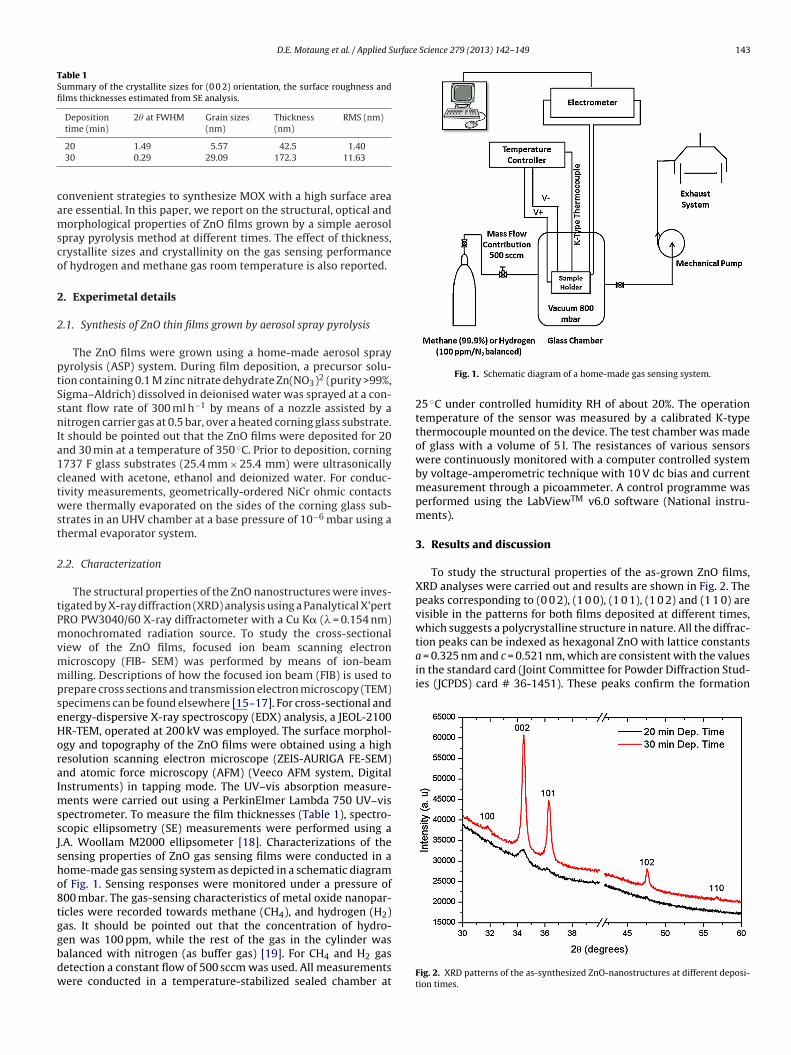
D.E. Motaung et al. / Applied Surface Science 279 (2013) 142– 149 143
Table 1Summary of the crystallite sizes for (0 0 2) orientation, the surface roughness andfilms thicknesses estimated from SE analysis.
Depositiontime (min)
2� at FWHM Grain sizes(nm)
Thickness(nm)
RMS (nm)
camsco
2
2
ptSsnIa1ctwst
2
tPmvmmpseHoraImssJsho8tggbdw
tion peaks can be indexed as hexagonal ZnO with lattice constantsa = 0.325 nm and c = 0.521 nm, which are consistent with the valuesin the standard card (Joint Committee for Powder Diffraction Stud-ies (JCPDS) card # 36-1451). These peaks confirm the formation
20 1.49 5.57 42.5 1.4030 0.29 29.09 172.3 11.63
onvenient strategies to synthesize MOX with a high surface areare essential. In this paper, we report on the structural, optical andorphological properties of ZnO films grown by a simple aerosol
pray pyrolysis method at different times. The effect of thickness,rystallite sizes and crystallinity on the gas sensing performancef hydrogen and methane gas room temperature is also reported.
. Experimetal details
.1. Synthesis of ZnO thin films grown by aerosol spray pyrolysis
The ZnO films were grown using a home-made aerosol sprayyrolysis (ASP) system. During film deposition, a precursor solu-ion containing 0.1 M zinc nitrate dehydrate Zn(NO3)2 (purity >99%,igma–Aldrich) dissolved in deionised water was sprayed at a con-tant flow rate of 300 ml h−1 by means of a nozzle assisted by aitrogen carrier gas at 0.5 bar, over a heated corning glass substrate.
t should be pointed out that the ZnO films were deposited for 20nd 30 min at a temperature of 350 ◦C. Prior to deposition, corning737 F glass substrates (25.4 mm × 25.4 mm) were ultrasonicallyleaned with acetone, ethanol and deionized water. For conduc-ivity measurements, geometrically-ordered NiCr ohmic contactsere thermally evaporated on the sides of the corning glass sub-
trates in an UHV chamber at a base pressure of 10−6 mbar using ahermal evaporator system.
.2. Characterization
The structural properties of the ZnO nanostructures were inves-igated by X-ray diffraction (XRD) analysis using a Panalytical X’pertRO PW3040/60 X-ray diffractometer with a Cu K� (� = 0.154 nm)onochromated radiation source. To study the cross-sectional
iew of the ZnO films, focused ion beam scanning electronicroscopy (FIB- SEM) was performed by means of ion-beamilling. Descriptions of how the focused ion beam (FIB) is used to
repare cross sections and transmission electron microscopy (TEM)pecimens can be found elsewhere [15–17]. For cross-sectional andnergy-dispersive X-ray spectroscopy (EDX) analysis, a JEOL-2100R-TEM, operated at 200 kV was employed. The surface morphol-gy and topography of the ZnO films were obtained using a highesolution scanning electron microscope (ZEIS-AURIGA FE-SEM)nd atomic force microscopy (AFM) (Veeco AFM system, Digitalnstruments) in tapping mode. The UV–vis absorption measure-
ents were carried out using a PerkinElmer Lambda 750 UV–vispectrometer. To measure the film thicknesses (Table 1), spectro-copic ellipsometry (SE) measurements were performed using a.A. Woollam M2000 ellipsometer [18]. Characterizations of theensing properties of ZnO gas sensing films were conducted in aome-made gas sensing system as depicted in a schematic diagramf Fig. 1. Sensing responses were monitored under a pressure of00 mbar. The gas-sensing characteristics of metal oxide nanopar-icles were recorded towards methane (CH4), and hydrogen (H2)as. It should be pointed out that the concentration of hydro-
en was 100 ppm, while the rest of the gas in the cylinder wasalanced with nitrogen (as buffer gas) [19]. For CH4 and H2 gasetection a constant flow of 500 sccm was used. All measurementsere conducted in a temperature-stabilized sealed chamber atFig. 1. Schematic diagram of a home-made gas sensing system.
25 ◦C under controlled humidity RH of about 20%. The operationtemperature of the sensor was measured by a calibrated K-typethermocouple mounted on the device. The test chamber was madeof glass with a volume of 5 l. The resistances of various sensorswere continuously monitored with a computer controlled systemby voltage-amperometric technique with 10 V dc bias and currentmeasurement through a picoammeter. A control programme wasperformed using the LabViewTM v6.0 software (National instru-ments).
3. Results and discussion
To study the structural properties of the as-grown ZnO films,XRD analyses were carried out and results are shown in Fig. 2. Thepeaks corresponding to (0 0 2), (1 0 0), (1 0 1), (1 0 2) and (1 1 0) arevisible in the patterns for both films deposited at different times,which suggests a polycrystalline structure in nature. All the diffrac-
Fig. 2. XRD patterns of the as-synthesized ZnO-nanostructures at different deposi-tion times.
144 D.E. Motaung et al. / Applied Surface Science 279 (2013) 142– 149
0 min
oidpo〈f3
fiwTHwt
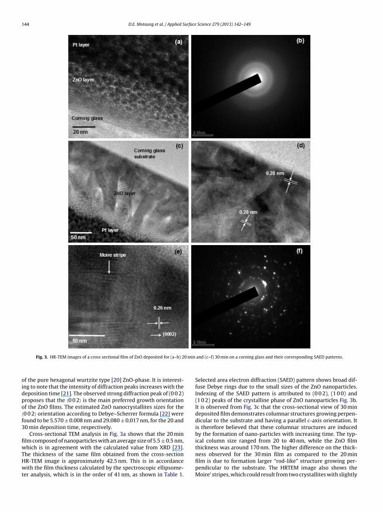
Fig. 3. HR-TEM images of a cross sectional film of ZnO deposited for (a–b) 2
f the pure hexagonal wurtzite type [20] ZnO-phase. It is interest-ng to note that the intensity of diffraction peaks increases with theeposition time [21]. The observed strong diffraction peak of (0 0 2)roposes that the 〈0 0 2〉 is the main preferred growth orientationf the ZnO films. The estimated ZnO nanocrystallites sizes for the0 0 2〉 orientation according to Debye–Scherrer formula [22] wereound to be 5.570 ± 0.008 nm and 29.080 ± 0.017 nm, for the 20 and0 min deposition time, respectively.
Cross-sectional TEM analysis in Fig. 3a shows that the 20 minlm composed of nanoparticles with an average size of 5.5 ± 0.5 nm,hich is in agreement with the calculated value from XRD [23].
he thickness of the same film obtained from the cross-sectionR-TEM image is approximately 42.5 nm. This is in accordanceith the film thickness calculated by the spectroscopic ellipsome-
er analysis, which is in the order of 41 nm, as shown in Table 1.
and (c–f) 30 min on a corning glass and their corresponding SAED patterns.
Selected area electron diffraction (SAED) pattern shows broad dif-fuse Debye rings due to the small sizes of the ZnO nanoparticles.Indexing of the SAED pattern is attributed to (0 0 2), (1 0 0) and(1 0 2) peaks of the crystalline phase of ZnO nanoparticles Fig. 3b.It is observed from Fig. 3c that the cross-sectional view of 30 mindeposited film demonstrates columnar structures growing perpen-dicular to the substrate and having a parallel c-axis orientation. Itis therefore believed that these columnar structures are inducedby the formation of nano-particles with increasing time. The typ-ical column size ranged from 20 to 40 nm, while the ZnO filmthickness was around 170 nm. The higher difference on the thick-
ness observed for the 30 min film as compared to the 20 minfilm is due to formation larger “rod-like” structure growing per-pendicular to the substrate. The HRTEM image also shows theMoire’ stripes, which could result from two crystallites with slightly
D.E. Motaung et al. / Applied Surface Science 279 (2013) 142– 149 145
nal vie
ds(pa
Eap
Fc
Fig. 4. The EDX spectra extracted at the cross-sectio
ifferent orientation. Fringe widths of 0.26, 0.28, and 0.19 nm mea-ured on different micrographs revealed the dominance of the0 0 2), (1 0 0) and (1 0 2) planes. This was consistent with the SAEDattern shown in Fig. 3f denoting that the ZnO columnar structuresre polycrystalline in nature.
To gain insight on the composition of the ZnO films, typicalDX elemental analysis was performed on a cross-sectional views demonstrated in Fig. 4. The EDX analysis for both ZnO filmsrepared at 20 and 30 min indicate a pure ZnO without any other
ig. 5. High-resolution SEM micrographs of ZnO films deposited by spray pyrolysis for (orning glass substrate.
w of ZnO films grown for (a) 20 min and (b) 30 min.
impurities. It is worthy to point out that the peaks at 1.0, 1.8 and8.1 keV are from the substrate and copper grid used in TEM analysis,respectively.
Fig. 5 shows the SEM micrographs of the ZnO films grownat different times. Spherical or agglomerated nanoparticles were
observed across the film (Fig. 5a). Fig. 5b shows ZnO nanostruc-tures grown for 30 min on a corning glass substrate. These ZnOnanorods were found to grow perpendicular to the substrate,entangled to one another forming “spaghetti-like” structures.a) 20 min, (b) 30 min and (c) a cross sectional view of the film prepared by ASP on
146 D.E. Motaung et al. / Applied Surface Science 279 (2013) 142– 149
ZnO fi
T2F
tncml“ciwi
oitosSine
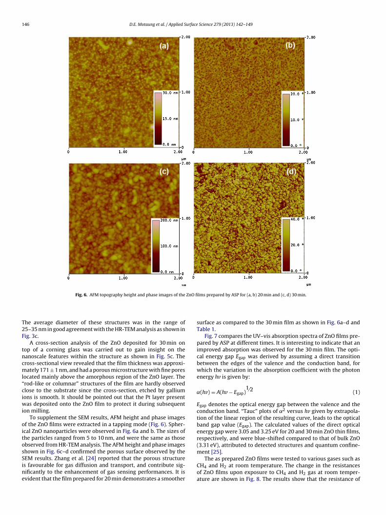
Fig. 6. AFM topography height and phase images of the
he average diameter of these structures was in the range of5–35 nm in good agreement with the HR-TEM analysis as shown inig. 3c.
A cross-section analysis of the ZnO deposited for 30 min onop of a corning glass was carried out to gain insight on theanoscale features within the structure as shown in Fig. 5c. Theross-sectional view revealed that the film thickness was approxi-ately 171 ± 1 nm, and had a porous microstructure with fine pores
ocated mainly above the amorphous region of the ZnO layer. Therod-like or columnar” structures of the film are hardly observedlose to the substrate since the cross-section, etched by galliumons is smooth. It should be pointed out that the Pt layer present
as deposited onto the ZnO film to protect it during subsequenton milling.
To supplement the SEM results, AFM height and phase imagesf the ZnO films were extracted in a tapping mode (Fig. 6). Spher-cal ZnO nanoparticles were observed in Fig. 6a and b. The sizes ofhe particles ranged from 5 to 10 nm, and were the same as thosebserved from HR-TEM analysis. The AFM height and phase imageshown in Fig. 6c–d confirmed the porous surface observed by the
EM results. Zhang et al. [24] reported that the porous structures favourable for gas diffusion and transport, and contribute sig-ificantly to the enhancement of gas sensing performances. It isvident that the film prepared for 20 min demonstrates a smootherlms prepared by ASP for (a, b) 20 min and (c, d) 30 min.
surface as compared to the 30 min film as shown in Fig. 6a–d andTable 1.
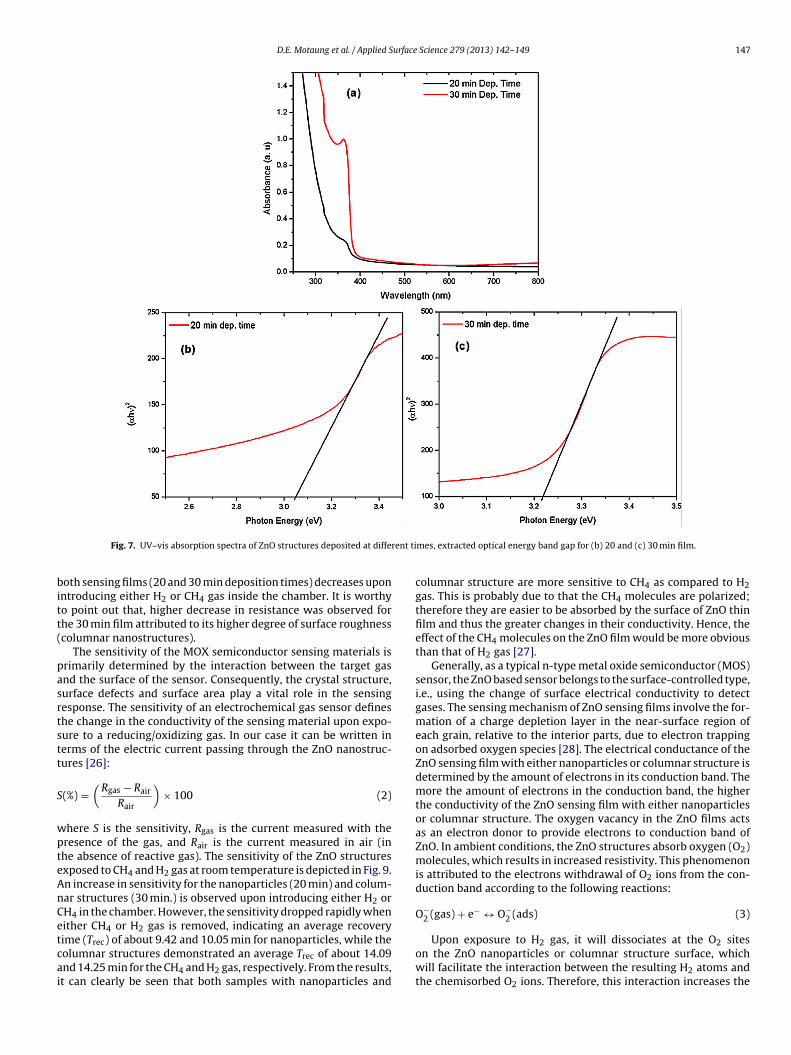
Fig. 7 compares the UV–vis absorption spectra of ZnO films pre-pared by ASP at different times. It is interesting to indicate that animproved absorption was observed for the 30 min film. The opti-cal energy gap Egap was derived by assuming a direct transitionbetween the edges of the valence and the conduction band, forwhich the variation in the absorption coefficient with the photonenergy hv is given by:
˛(hv) = A(hv − Egap)1⁄2 (1)
Egap denotes the optical energy gap between the valence and theconduction band. “Tauc” plots of ˛2 versus hv given by extrapola-tion of the linear region of the resulting curve, leads to the opticalband gap value (Egap). The calculated values of the direct opticalenergy gap were 3.05 and 3.25 eV for 20 and 30 min ZnO thin films,respectively, and were blue-shifted compared to that of bulk ZnO(3.31 eV), attributed to detected structures and quantum confine-ment [25].
The as prepared ZnO films were tested to various gases such asCH4 and H2 at room temperature. The change in the resistancesof ZnO films upon exposure to CH4 and H2 gas at room temper-ature are shown in Fig. 8. The results show that the resistance of
D.E. Motaung et al. / Applied Surface Science 279 (2013) 142– 149 147
rent ti
bitt(
pasrtstt
S
wpteAnCetcai
Fig. 7. UV–vis absorption spectra of ZnO structures deposited at diffe
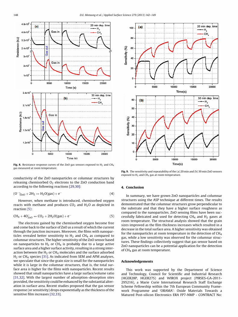
oth sensing films (20 and 30 min deposition times) decreases uponntroducing either H2 or CH4 gas inside the chamber. It is worthyo point out that, higher decrease in resistance was observed forhe 30 min film attributed to its higher degree of surface roughnesscolumnar nanostructures).
The sensitivity of the MOX semiconductor sensing materials isrimarily determined by the interaction between the target gasnd the surface of the sensor. Consequently, the crystal structure,urface defects and surface area play a vital role in the sensingesponse. The sensitivity of an electrochemical gas sensor defineshe change in the conductivity of the sensing material upon expo-ure to a reducing/oxidizing gas. In our case it can be written inerms of the electric current passing through the ZnO nanostruc-ures [26]:
(%) =(
Rgas − Rair
Rair
)× 100 (2)
here S is the sensitivity, Rgas is the current measured with theresence of the gas, and Rair is the current measured in air (inhe absence of reactive gas). The sensitivity of the ZnO structuresxposed to CH4 and H2 gas at room temperature is depicted in Fig. 9.n increase in sensitivity for the nanoparticles (20 min) and colum-ar structures (30 min.) is observed upon introducing either H2 orH4 in the chamber. However, the sensitivity dropped rapidly whenither CH4 or H2 gas is removed, indicating an average recovery
ime (Trec) of about 9.42 and 10.05 min for nanoparticles, while theolumnar structures demonstrated an average Trec of about 14.09nd 14.25 min for the CH4 and H2 gas, respectively. From the results,t can clearly be seen that both samples with nanoparticles andmes, extracted optical energy band gap for (b) 20 and (c) 30 min film.
columnar structure are more sensitive to CH4 as compared to H2gas. This is probably due to that the CH4 molecules are polarized;therefore they are easier to be absorbed by the surface of ZnO thinfilm and thus the greater changes in their conductivity. Hence, theeffect of the CH4 molecules on the ZnO film would be more obviousthan that of H2 gas [27].
Generally, as a typical n-type metal oxide semiconductor (MOS)sensor, the ZnO based sensor belongs to the surface-controlled type,i.e., using the change of surface electrical conductivity to detectgases. The sensing mechanism of ZnO sensing films involve the for-mation of a charge depletion layer in the near-surface region ofeach grain, relative to the interior parts, due to electron trappingon adsorbed oxygen species [28]. The electrical conductance of theZnO sensing film with either nanoparticles or columnar structure isdetermined by the amount of electrons in its conduction band. Themore the amount of electrons in the conduction band, the higherthe conductivity of the ZnO sensing film with either nanoparticlesor columnar structure. The oxygen vacancy in the ZnO films actsas an electron donor to provide electrons to conduction band ofZnO. In ambient conditions, the ZnO structures absorb oxygen (O2)molecules, which results in increased resistivity. This phenomenonis attributed to the electrons withdrawal of O2 ions from the con-duction band according to the following reactions:
O−2 (gas) + e− ↔ O−
2 (ads) (3)
Upon exposure to H2 gas, it will dissociates at the O2 siteson the ZnO nanoparticles or columnar structure surface, whichwill facilitate the interaction between the resulting H2 atoms andthe chemisorbed O2 ions. Therefore, this interaction increases the
148 D.E. Motaung et al. / Applied Surface Science 279 (2013) 142– 149
Fg
cra
(
rr
C
attcosaHwwfs[pars
ig. 8. Resistance response curves of the ZnO gas sensors exposed to H2 and CH4
as measured at room temperature.
onductivity of the ZnO nanoparticles or columnar structures byeleasing chemisorbed O2 electrons to the ZnO conduction bandccording to the following reactions [29,30]:
O−)ZnO + 2H2 ↔ H2O(gas) + e− (4)
However, when methane is introduced, chemisorbed oxygeneacts with methane and produces CO2 and H2O as depicted ineaction (5):
H4 + 4O−ZnO ↔ CO2 + 2H2O(gas) + e− (5)
The electrons gained by the chemisorbed oxygen become freend come back to the surface of ZnO as a result of which the currenthrough the junction increases. Moreover, the films with nanopar-icles revealed better sensitivity to H2 and CH4 as compared toolumnar structures. The higher sensitivity of the ZnO sensor basedn nanoparticles to H2 or CH4 is probably due to a large activeurface area and a higher surface activity, resulting in a strong inter-ction between the H2 or CH4 molecules and the surface adsorbed2 or CH4 species [31]. As indicated from SEM and AFM analyses,e speculate that since the grain size is small for the nanoparticleshile it is large in the columnar structures, that is, the total sur-
ace area is higher for the films with nanoparticles. Recent resultshowed that small nanoparticles have a large surface/volume ratio31,32]. With the largest number of adsorption–desorption sites
rovided, the sensitivity could be enhanced by the substantial alter-tion in surface area. Recent studies proposed that the gas sensoresponse (or sensitivity) drops exponentially as the thickness of theensitive film increases [32,33].Fig. 9. The sensitivity and repeatability of the (a) 20 min and (b) 30 min ZnO sensorsexposed to H2 and CH4 gas at room temperature.
4. Conclusion
In summary, we have grown ZnO nanoparticles and columnarstructures using the ASP technique at different times. The resultsdemonstrated that the columnar structures grow perpendicular tothe substrate and that they have a higher surface roughness ascompared to the nanoparticles. ZnO sensing films have been suc-cessfully fabricated and used for detecting CH4 and H2 gases atroom temperature. The structural analysis showed that the grainsizes improved as the film thickness increases which resulted in adecrease in the total surface area. A higher sensitivity was obtainedfor the nanoparticles at room temperature in the detection of CH4gas, while a low sensitivity was observed for the columnar struc-tures. These findings collectively suggest that gas sensor based onZnO nanoparticles can be a potential application for the detectionof CH4 gas at room temperature.
Acknowledgements
This work was supported by the Department of Scienceand Technology, Council for Scientific and Industrial Research(HGER28P, HGER27S) and WIROX project (PIRSES-GA-2011-295216), a Marie Curie International Research Staff Exchange
Scheme Fellowship within the 7th European Community Frame-work Programme and ‘ORAMA’: Oxide Materials Towards aMatured Post-silicon Electronics ERA FP7-NMP - CONTRACT No:
urface
2b
R
[[
[[
[[
[[
[
[
[
[[
[
[
[
[
[
[
D.E. Motaung et al. / Applied S
46334. The authors are also thankful to the equipment suppliedy the NCNSMs and FORTH institute for the analysis.
eferences
[1] R. Ferro, J.A. Rodriguez, P. Bertrand, Thin Solid Films 556 (2008) 2225.[2] P. Moriarty, D. Honnery, International Journal of Hydrogen Energy 34 (2009)
31.[3] G. Sberveglieri, Sensors and Actuators B 23 (1995) 103.[4] O.D. Jayakumar, N. Manoj, V. Sudarsan, C.G.S. Pillai, A.K. Tyagi, CrystEngComm
13 (2011) 2187.[5] J.X. Wang, X.W. Sun, Y. Yang, C.M.L Wu, Nanotechnology 20 (2009) 465501.[6] Y. Zeng, T. Zhang, L. Wang, M. Kang, H. Fan, R. Wang, et al., Sensors and Actuators
B 140 (2009) 73.[7] T. Krishnakumar, R. Jayaprakash, N. Pinna, N. Donato, A. Bonavita, G. Micali,
et al., Sensors and Actuators B 143 (2009) 198.[8] J.H. Lee, Sensors and Actuators B 140 (2009) 319.[9] N. Yamazoe, K. Shimanoe, Journal of the Electrochemical Society 155 (2008)
85.10] J. Chen, L.N. Xu, W.Y. Li, X.H. Gou, Advanced Materials 17 (2005) 582.11] J. Sun, J. Xu, Y.S. Yu, P. Sun, F. Liu, G. Lu, Sensors and Actuators B: Chemical
(2012), http://dx.doi.org/10.1016/j.snb.2012.04.083.12] K.J. Choi, H.W. Jang, Sensors 10 (2010) 4083.
13] Z.C. Wu, K. Yu, S.D. Zhang, Y. Xie, Journal of Physical Chemistry C 112 (2008)11307.14] B.X. Li, Y. Xie, M. Jing, G.X. Rong, Y.C. Tang, G.Z. Zhang, Langmuir 22 (2006) 9380.15] J. Orloff, M. Utlaut, L. Swanson, High Resolution Focused Ion Beams: FIB and Its
Applications, Kluwer Academic/Plenum Publishers, New York, 2003.
[[[[[
Science 279 (2013) 142– 149 149
16] N. Rowlands, P.R. Munroe, Microstructural Science 26 (1998) 233.17] M.H.F. Overwijk, F.C. Van den Heuvel, C.W.T. Sulle-Lieuwma, Journal of Vacuum
Science & Technology B 11 (1993) 2021.18] D.E. Motaung, G.F. Malgas, C.J. Arendse, S.E. Mavundla, Materials Chemistry and
Physics 135 (2012) 401.19] N. Al-Hardan, M.J. Abdullah, A.A. Aziz, Applied Surface Science 255 (2009)
7794.20] Z. Jiang, Z. Huang, P. Yang, J. Chen, Y. Xin, J. Xu, Composites Science and Tech-
nology 68 (2008) 3240.21] J.L. Van Heerden, R. Swanepoel, Thin Solid Films 299 (1997) 72.22] D. Cullity, Elements of X-ray Diffraction, Addison-Wesley, Reading, MA, 1956,
363.23] R. Viswanatha, S. Sapra, B. Satpati, P.V. Satyam, B.N. Dev, D.D. Sarma, Journal of
Materials Chemistry 14 (2004) 661.24] L. Zhang, J. Zhao, J. Zheng, L. Li, Z. Zhu, Sensors and Actuators B 158 (2011)
144.25] D.W. Bahnemann, C. Kormann, M.R. Hoffmann, Journal of Physical Chemistry
91 (1987) 3789.26] N.S. Ramgir, M. Ghosh, P. Veerender, N. Datta, M. Kaur, D.K. Aswal, S.K. Gupta,
Sensors and Actuators B: Chemical 156 (2011) 875.27] X.Y. Penga, M. Sajjada, J. Chua, B.Q. Yangb, P.X. Feng, Applied Surface Science
257 (2011) 4795.28] A. Kolmakov, Y. Zhang, G. Cheng, M. Moskovits, Advanced Materials 15 (2003)
997.
29] O. Lupan, G. Chai, L. Chow, Microelectronic Engineering 85 (2008) 2220.30] A.D.S. Basu, Materials Chemistry and Physics 47 (1997) 93.31] S. Basu, P.K. Basu, Journal of Sensors (2009) 20, Article ID 861968.32] F. Hossein-Babaei, M. Orvatinia, Sensors and Actuators B 89 (2003) 256.33] J.C. Li, X.B. Han, Y.H. Jiang, D.C. Ba, Thin Solid Films 520 (2011) 881.