Analysis of InGaN Quantum Wells with AlGaInN Barriers - CORE
49
Lehigh University Lehigh Preserve eses and Dissertations 2018 Analysis of InGaN Quantum Wells with AlGaInN Barriers Hanlin Fu Lehigh University Follow this and additional works at: hps://preserve.lehigh.edu/etd Part of the Electrical and Computer Engineering Commons is esis is brought to you for free and open access by Lehigh Preserve. It has been accepted for inclusion in eses and Dissertations by an authorized administrator of Lehigh Preserve. For more information, please contact [email protected]. Recommended Citation Fu, Hanlin, "Analysis of InGaN Quantum Wells with AlGaInN Barriers" (2018). eses and Dissertations. 2984. hps://preserve.lehigh.edu/etd/2984
-
Upload
khangminh22 -
Category
Documents
-
view
4 -
download
0
Transcript of Analysis of InGaN Quantum Wells with AlGaInN Barriers - CORE
Lehigh UniversityLehigh Preserve
Theses and Dissertations
2018
Analysis of InGaN Quantum Wells with AlGaInNBarriersHanlin FuLehigh University
Follow this and additional works at: https://preserve.lehigh.edu/etd
Part of the Electrical and Computer Engineering Commons
This Thesis is brought to you for free and open access by Lehigh Preserve. It has been accepted for inclusion in Theses and Dissertations by anauthorized administrator of Lehigh Preserve. For more information, please contact [email protected].
Recommended CitationFu, Hanlin, "Analysis of InGaN Quantum Wells with AlGaInN Barriers" (2018). Theses and Dissertations. 2984.https://preserve.lehigh.edu/etd/2984
Analysis of InGaN Quantum Wells with AlGaInN
Barriers
By
Hanlin Fu
A Thesis
Presented to the Graduate and Research Committee
Of Lehigh University
In Candidacy for the Degree of
Master of Science
in
Electrical Engineering
Lehigh University
December, 2017
i
This thesis is accepted and approved in partial fulfillment of the requirements for a
Master’s of Science.
Date: December 14th 2017
Prof. Nelson Tansu, MS Thesis Advisor
Daniel E. '39 and Patricia M. Smith Endowed Chair Professor
Director, Center for Photonics and Nanoelectronics
Prof. Chengshan Xiao
Chair of Electrical and Computer Engineering Department
ii
Acknowledgement
I would first like to thank my advisor Professor Nelson Tansu. I have been working and
studying in Prof. Tansu’s lab for one year. During this year, I have learned greatly from Prof. Tansu
not only in terms of scientific and technical knowledge, but also via profound life principles that
he has illustrated by personal example. I benefit a lot from listening to his discussion in the lab.
For instance, I now further appreciate the importance of persistence and focus in both study and
life, which I aspire to follow in rest of my life. I also do believe that I learn a great deal on the
values of honesty, integrity, and responsibility from the experience working together with my
advisor. For this, I truly value this learning experience. I appreciate the significant help from
Prof.Tansu in my research and I am proud to be his student.
I am also thankful for my family for financially and emotionally supporting me through all
my graduate studies in Lehigh University. Whenever I was in trouble and confused about the
future, my mother would give me the best comfort and support me in conquering any difficulties.
My family always provided me a solid backing and I appreciate all the effort they made to help
me.
Finally, I would like to thank all my friends, without whom I could not have gone this far.
My lab colleagues Prof. Jonathan Wierer, Dr. Renbo Song, Xiongliang Wei, Wei Sun, Austin
Slosberg, Justin Goodrich, Damir Baravoc, Ioannis Fragkos, Onos Ogidi-Ekoko, Syed Ahmed Al
Muyeed, Matthew Peart, Qingyang Li, Jiaheng Wu, and Tianfei Song all provide me great help on
my research and study. My roommates Lei Li and Yuan Li offer me great enjoyment in life. It’s my
best fortune to live and study with you.
iii
Table of Contents
Acknowledgement………………………………………………………………………………………………………….…….…..ii
List of Figures……………….…………………………………………………………………………………………………….…….v
List of Tables……………….…………………………………………………………………………………………………….…….vii
Abstract………………………………………………………………………………………………………………………………...….1
1. Introduction ………………………………………………………………………………………………………………….2
1.1. Brief History of Conventional InGaN-Based Devices………………………………......……..2
1.2. Challenges of Conventional InGaN Lasers and LEDs………………………..………...……...4
1.3. Strain-Compensated InGaN-InGaAlN Quantum Wells………………………………….…..…4
1.4. Thesis Organization ………………………………………………………………………………….……….5
2. Self-Consistent 6-Band k∙p Method for III-Nitride Semiconductors………………………….…….7
2.1. The Hamiltonian Matrix Elements for 6-Band k∙p Method …………………….……..…..7
2.2. The Spontaneous and Piezoelectric Polarizations Characteristics …………………...…9
2.3. Momentum Matrix Elements and Fermi’s Golden Rule…………………………............10
2.4. Self-Consistent Schrödinger and Poisson Equations………………………………………….13
2.5 Summary………………………………………………………………………………………………………….15
3. Band Properties for InGaN-AlGaInN Quantum Wells…....…………………..………………………...16
3.1. Band Lineups and Carrier Concentration Distributions.………………………….…….....16
3.2. Valence Band Structures………………………………………………………………….……….….….18
3.3 Momentum Matrix Elements Characteristics………………………………………………...…20
3.4 Summary…………………………………………………………………………………………………………..23
4. Optical Properties of InGaN-AlGaInN Quantum Wells………………..…………………………..……24
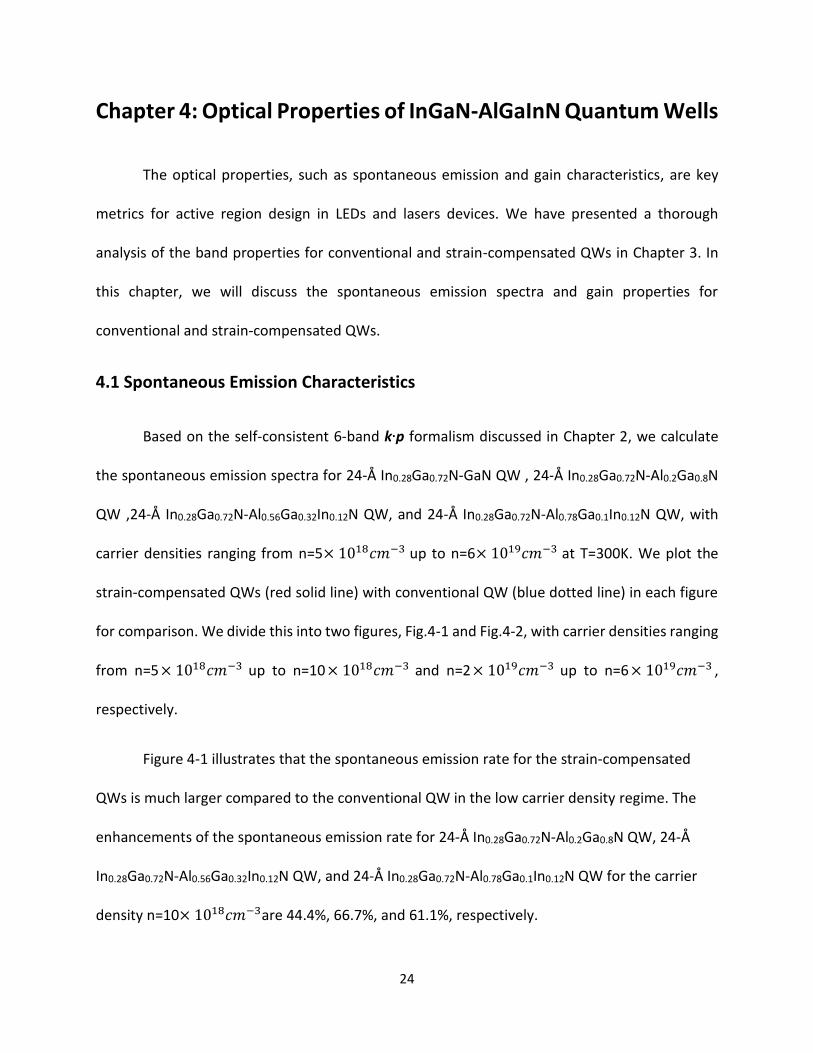
4.1. Spontaneous Emission Characteristics……………………………………………….……………..24
iv
4.2. Optical Gain Characteristics…………………….……………………………..…………..……………30
4.3 Summary…………………………………………………………………………………………………….…...34
5. Conclusion………………………….…………………………….………….……………………………………………...35
References…………………………………………………………………………………………………………….…………….…..37
Vita..………………………………………………………………………………………………………………………………..………40
v
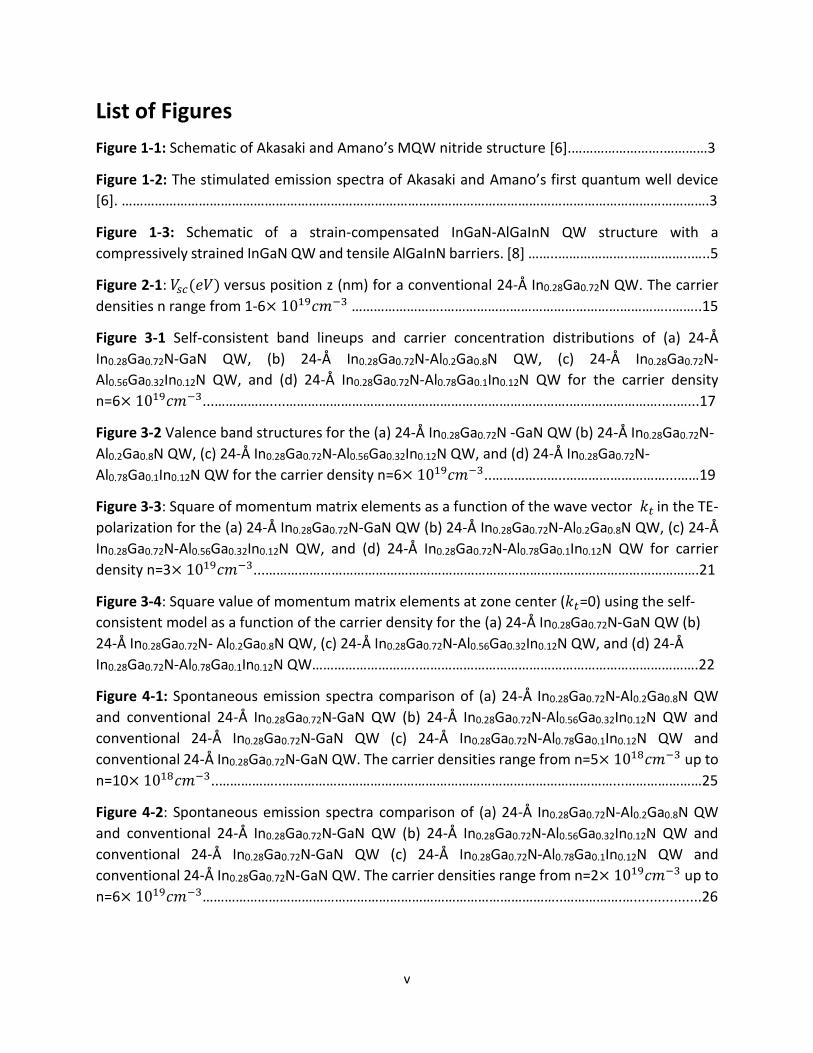
List of Figures
Figure 1-1: Schematic of Akasaki and Amano’s MQW nitride structure [6].…………………….…………3
Figure 1-2: The stimulated emission spectra of Akasaki and Amano’s first quantum well device
[6]. …………………………………………………………………………………………………………………………………………….3
Figure 1-3: Schematic of a strain-compensated InGaN-AlGaInN QW structure with a
compressively strained InGaN QW and tensile AlGaInN barriers. [8] ……..……………….……………..…..5
Figure 2-1: 𝑉𝑠𝑐(𝑒𝑉) versus position z (nm) for a conventional 24-Å In0.28Ga0.72N QW. The carrier
densities n range from 1-6× 10¹⁹𝑐𝑚−3 …………………….……………………………………………………..……..15
Figure 3-1 Self-consistent band lineups and carrier concentration distributions of (a) 24-Å
In0.28Ga0.72N-GaN QW, (b) 24-Å In0.28Ga0.72N-Al0.2Ga0.8N QW, (c) 24-Å In0.28Ga0.72N-
Al0.56Ga0.32In0.12N QW, and (d) 24-Å In0.28Ga0.72N-Al0.78Ga0.1In0.12N QW for the carrier density
n=6× 10¹⁹𝑐𝑚−3...……………....…………………………………………….…………………….…………………….….…...17
Figure 3-2 Valence band structures for the (a) 24-Å In0.28Ga0.72N -GaN QW (b) 24-Å In0.28Ga0.72N-
Al0.2Ga0.8N QW, (c) 24-Å In0.28Ga0.72N-Al0.56Ga0.32In0.12N QW, and (d) 24-Å In0.28Ga0.72N-
Al0.78Ga0.1In0.12N QW for the carrier density n=6× 10¹⁹𝑐𝑚−3..………………..………………………...……19
Figure 3-3: Square of momentum matrix elements as a function of the wave vector 𝑘𝑡 in the TE-
polarization for the (a) 24-Å In0.28Ga0.72N-GaN QW (b) 24-Å In0.28Ga0.72N-Al0.2Ga0.8N QW, (c) 24-Å
In0.28Ga0.72N-Al0.56Ga0.32In0.12N QW, and (d) 24-Å In0.28Ga0.72N-Al0.78Ga0.1In0.12N QW for carrier
density n=3× 10¹⁹𝑐𝑚−3...……………………………………………………………………………………………………….21
Figure 3-4: Square value of momentum matrix elements at zone center (𝑘𝑡=0) using the self-
consistent model as a function of the carrier density for the (a) 24-Å In0.28Ga0.72N-GaN QW (b)
24-Å In0.28Ga0.72N- Al0.2Ga0.8N QW, (c) 24-Å In0.28Ga0.72N-Al0.56Ga0.32In0.12N QW, and (d) 24-Å
In0.28Ga0.72N-Al0.78Ga0.1In0.12N QW………………………..………………………………………………………………….22
Figure 4-1: Spontaneous emission spectra comparison of (a) 24-Å In0.28Ga0.72N-Al0.2Ga0.8N QW
and conventional 24-Å In0.28Ga0.72N-GaN QW (b) 24-Å In0.28Ga0.72N-Al0.56Ga0.32In0.12N QW and
conventional 24-Å In0.28Ga0.72N-GaN QW (c) 24-Å In0.28Ga0.72N-Al0.78Ga0.1In0.12N QW and
conventional 24-Å In0.28Ga0.72N-GaN QW. The carrier densities range from n=5× 10¹⁸𝑐𝑚−3 up to
n=10× 1018𝑐𝑚−3..……………..………………………………………………………………………………...…………………25
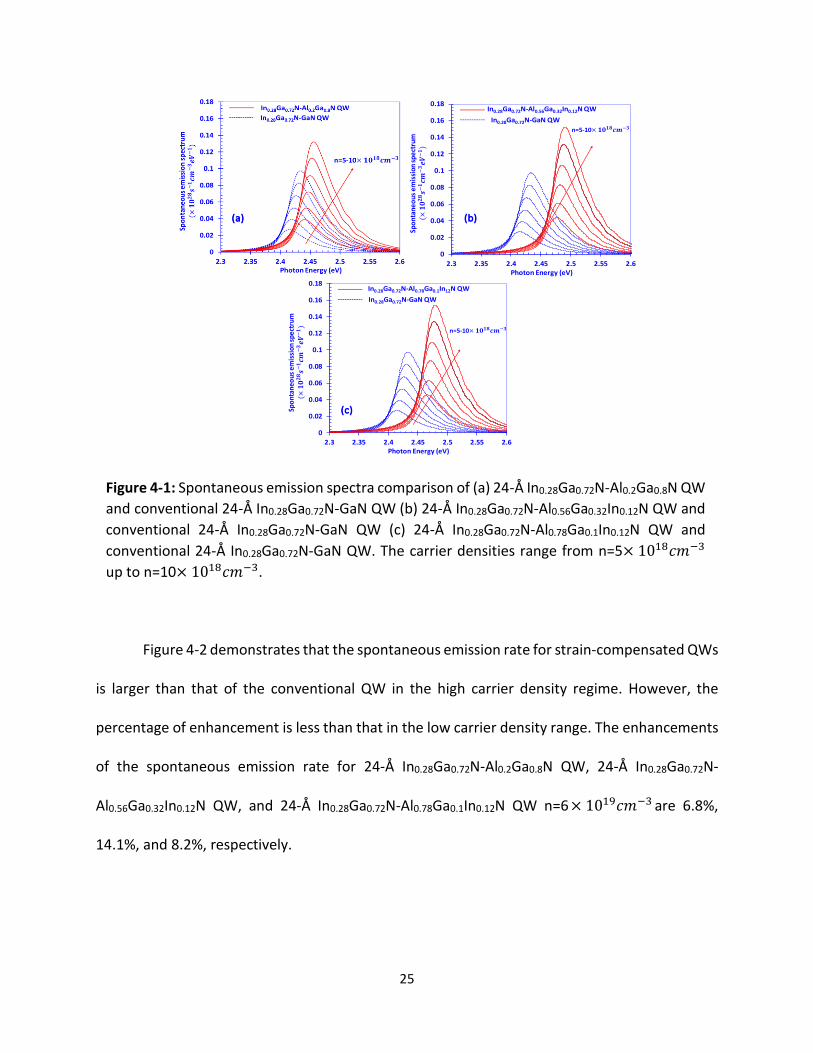
Figure 4-2: Spontaneous emission spectra comparison of (a) 24-Å In0.28Ga0.72N-Al0.2Ga0.8N QW
and conventional 24-Å In0.28Ga0.72N-GaN QW (b) 24-Å In0.28Ga0.72N-Al0.56Ga0.32In0.12N QW and
conventional 24-Å In0.28Ga0.72N-GaN QW (c) 24-Å In0.28Ga0.72N-Al0.78Ga0.1In0.12N QW and
conventional 24-Å In0.28Ga0.72N-GaN QW. The carrier densities range from n=2× 10¹⁹𝑐𝑚−3 up to
n=6× 10¹⁹𝑐𝑚−3……………………………………………………………………………………..…………….….................26
vi
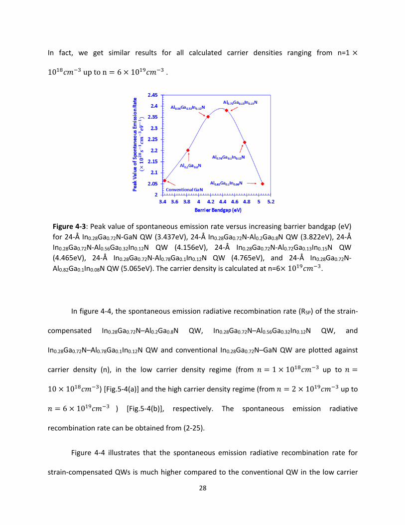
Figure 4-3: Peak value of spontaneous emission rate versus increasing barrier bandgap (eV) for
24-Å In0.28Ga0.72N-GaN QW (3.437eV), 24-Å In0.28Ga0.72N-Al0.2Ga0.8N QW (3.822eV), 24-Å
In0.28Ga0.72N-Al0.56Ga0.32In0.12N QW (4.156eV), 24-Å In0.28Ga0.72N-Al0.72Ga0.13In0.15N QW (4.465eV),
24-Å In0.28Ga0.72N-Al0.78Ga0.1In0.12N QW (4.765eV), and 24-Å In0.28Ga0.72N-Al0.82Ga0.1In0.08N QW
(5.065eV). The carrier density is calculated at n=6× 10¹⁹𝑐𝑚−3....………………………….……..…………28
Figure 4-4: S Spontaneous emission radiative recombination rate comparison as a function of
carrier density at 300K for 24-Å In0.28Ga0.72N-Al0.2Ga0.8N QW, 24-Å In0.28Ga0.72N-Al0.56Ga0.32In0.12N
QW, 24-Å In0.28Ga0.72N-Al0.78Ga0.1In0.12N QW, and 24-Å In0.28Ga0.72N-GaN QW. The carrier densities
range from (a) n=1 × 10¹⁸𝑐𝑚−3 up to n=10 × 1018𝑐𝑚−3 and (b) n=1 × 10¹⁹𝑐𝑚−3 up to
n=6× 10¹⁹𝑐𝑚−3…………………………………………………………...…………………………………………..…………….29
Figure 4-5: Ratio of spontaneous emission radiative recombination rate (RSP) for strain
compensated 24-Å In0.28Ga0.72N-Al0.2Ga0.8N QW, 24-Å In0.28Ga0.72N-Al0.56Ga0.32In0.12N QW, 24-Å
In0.28Ga0.72N-Al0.78Ga0.1In0.12N QW, and conventional 24-Å In0.28Ga0.72N-GaN QW as function of
carrier density at temperature of 300K. The ratio is plotted from n=1× 10¹⁸𝑐𝑚−3 up to
n=6× 10¹⁹𝑐𝑚−3..…………………………….………………………………………………………………………..……...…….30
Figure 4-6: TE-polarized optical gain spectra of strain-compensated 24-Å In0.28Ga0.72N-Al0.2Ga0.8N
QW (a), 24-Å In0.28Ga0.72N-Al0.56Ga0.32In0.12N QW (b), and 24-Å In0.28Ga0.72N-Al0.78Ga0.1In0.12N QW
(c) compared to the conventional 24-Å In0.28Ga0.72N-GaN QW for carrier density (n) from
n=3× 10¹⁹𝑐𝑚−3 up to n=6× 10¹⁹𝑐𝑚−3...………………..……………………..……………………………………….31
Figure 4-7: Peak material gain as a function of carrier density at 300 K for 24-Å In0.28Ga0.72N-
Al0.2Ga0.8N QW, 24-Å In0.28Ga0.72N-Al0.56Ga0.32In0.12N QW, 24-Å In0.28Ga0.72N-Al0.78Ga0.1In0.12N QW,
and 24-Å In0.28Ga0.72N-GaN QW for carrier densities range from n=1 × 10¹⁸𝑐𝑚−3 up to
n=6× 10¹⁹𝑐𝑚−3…………………………………………………………………………………..………………….…..………….32
Figure 4-8: Peak material gain versus increasing barrier bandgap (eV) for 24-Å In0.28Ga0.72N-GaN
QW (3.437eV), 24-Å In0.28Ga0.72N-Al0.2Ga0.8N QW (3.822eV), 24-Å In0.28Ga0.72N- Al0.56Ga0.32In0.12N
QW (4.156eV), 24-Å In0.28Ga0.72N-Al0.72Ga0.13In0.15N QW (4.465eV), 24-Å In0.28Ga0.72N-
Al0.78Ga0.1In0.12N QW (4.765eV), and 24-Å In0.28Ga0.72N-Al0.82Ga0.1In0.08N QW (5.065eV). The carrier
density is calculated at n=6× 10¹⁹𝑐𝑚−3...……………………………………..………..……..…..………………..…33
vii
List of Tables
Table 3-1: Material parameters for GaN, AlN, and InN. The values are taken from [21] …………….20
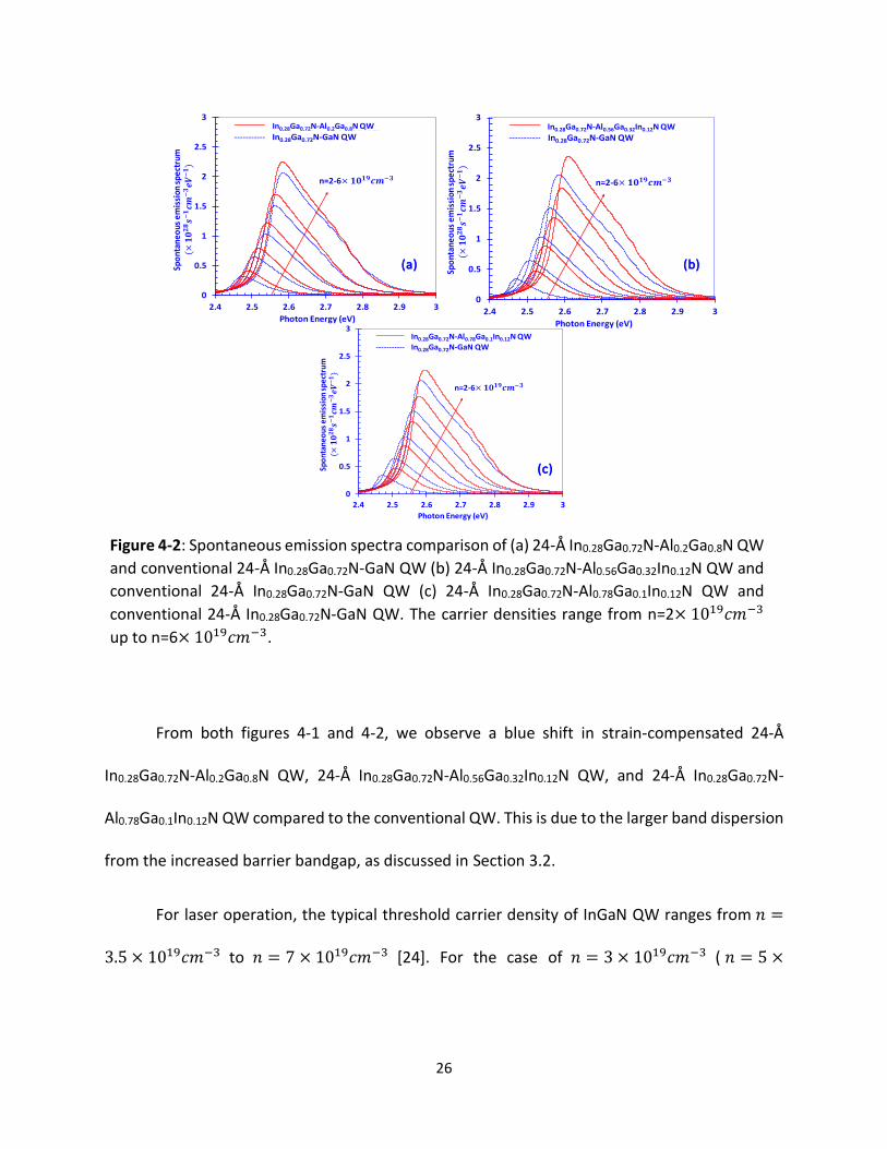
Table 4-1: Enhancement factors of the spontaneous emission rate for strain-compensated 24-Å
In0.28Ga0.72N- Al0.2Ga0.8N QW, 24-Å In0.28Ga0.72N-Al0.56Ga0.32In0.12N QW, and 24-Å In0.28Ga0.72N-
Al0.78Ga0.1In0.12N QW compared to conventional 24-Å In0.28Ga0.72N-GaN QW at transparency
(n=3× 10¹⁹𝑐𝑚−3) and near threshold (n=5× 10¹⁹𝑐𝑚−3).………………………………..…………….……….27
Table 4-2: Material gain and enhancement factors for strain-compensated 24-Å In0.28Ga0.72N-
Al0.2Ga0.8N QW, 24-Å In0.28Ga0.72N-Al0.56Ga0.32In0.12N QW, and 24-Å In0.28Ga0.72N-Al0.78Ga0.1In0.12N
QW compared to conventional 24-Å In0.28Ga0.72N-GaN QW near threshold (n=5 ×
1019𝑐𝑚−3)....................................................................................................................................33

1
Abstract
Various strain-compensated InGaN-AlGaInN quantum well (QW) structures are
investigated by self-consistent 6-band k∙p method, which considers valence band mixing, the
strain effect, spontaneous and piezoelectric polarizations and the carrier screening effect, for
their spontaneous emission and gain properties. The InGaN QW with In-content of 28% is
sandwiched by AlGaInN barriers, which are Al0.2Ga0.8N, Al0.56Ga0.32In0.12N, Al0.72Ga0.13In0.15N,
Al0.78Ga0.1In0.12N, and Al0.82Ga0.1In0.08N, with corresponding band gaps of 3.821eV, 4.156eV,
4.465eV, 4.765eV, and 5.065eV, respectively. Both the spontaneous emission spectra and optical
gain properties of strain-compensated InGaN–AlGaInN QWs reveal enhancement in comparison
to those of conventional InGaN–GN QWs. The enhancement factors of spontaneous emission
spectra and peak gain properties for different barrier structures are found to follow a parabolic
trend. This indicates differing amounts of improvement of the radiative efficiency for light
emitting diodes. This study shows that there is an optimized composition for an AlGaInN barrier
layer surrounding an In0.28Ga0.72N quantum well between the bandgaps of 4.156eV and 4.465eV
that will obtain the highest spontaneous emission rate and gain properties.

2
Chapter 1: Introduction
In this chapter, we present a brief introduction of the history and challenges for
conventional InGaN-based devices. We introduce the concept of the strain-compensated
quantum well and as well as present the organization of this thesis.
1.1 Brief History of Conventional InGaN-Based LEDs
III-Nitride based semiconductors, which are composed of GaN, InN and AlN and their
alloys, have changed the world for their amazing ability to emit a wide range of wavelengths in
the visible spectrum. The world’s first electroluminescence from a GaN film was reported and
published in May 1971, by J. I. Pankove et al [1]. H. M. Manasevit reported the first attempt of
the growth of thin film nitride samples by MOCVD (metal organic chemical vapor deposition)
process which he had pioneered in the same year [2]. In 1984, T. Kawabata et al. reported the
first blue GaN LED grown by the MOCVD [3]. The following fundamental breakthrough was the
world’s first nitride blue LED containing a p-n junction that was presented at a conference in Los
Angeles in 1989 [4]. In 1993, S. Nakamura et al. described their advanced p-GaN/n-InGaN/n-GaN
double heterojunction (DH) violet LEDs. Their InGaN/GaN DH LED emits blue light at a wavelength
of 420nm [5]. In November 1995, Akasaki and Amano reported the fabrication of a novel
InGaN/GaN quantum well structure. Their structure is shown in figure 1-1 [6]. Their first
observation of stimulated emission from a quantum well structure is shown in figure 1-2 [6]. For
the invention of efficient blue light-emitting diodes, which have enabled bright and energy-saving
white light sources, Akasaki, Amano, and Nakamura were awarded the 2014 Nobel Prize in

3
Physics [7]. Nowadays, InGaN based LEDs and lasers have become an irreplaceable technology
part for our everyday lives.
Figure 1-1: Schematic of Akasaki and Amano’s MQW nitride structure [6].
Figure 1-2: The stimulated emission spectra of Akasaki and Amano’s first quantum well device [6].
4
1.2 Challenges of Conventional InGaN Lasers and LEDs
Conventional III-nitride lasers and LEDs are developed based upon the InGaN QW as the
active region. There are two major challenges in InGaN QWs. The first is the low electron and
hole wave function overlap. This phenomenon is mainly caused by the large spontaneous and
piezoelectric polarization in the QW. The second limitation is the high dislocation density caused
by the strain-induced lattice mismatch between InGaN and GaN [8]. Previously published reports
indicate a significant improvement of optical gain and reduction of the threshold current density
by using a strain-compensated InGaN-Al0.2Ga0.8N QW structure with thin (~1-nm) tensile-
strained Al0.2Ga0.8N barriers to surround the compressively strained InGaN QW [8]. Reduction of
strain from this barrier structure results in a closer lattice match which in turn causes a lower
dislocation density in the lattice. The strain-compensated QW theory involved will be discussed
in Section 1.3.
1.3 Strain-Compensated InGaN-AlGaInN Quantum Well
A strain-compensated InGaN-AlGaInN QW is achieved by inserting an AlGaInN barrier
which lattice constant smaller than that of GaN to compensate the compressive strain of the
InGaN QW. In figure 1-3, we present the transformation process for each layer from an
unstrained status to the strain-compensated InGaN-AlGaInN QW. The employment of an AlGaInN
barrier results in a reduction of strain energy inside the compressive QW. The concept of strain-
compensated QWs was previously applied in InGaAsN QW and InGaAS QW active regions,
resulting in high performance 1200-1400nm emitting diode lasers on GaAs substrates [9] - [11].
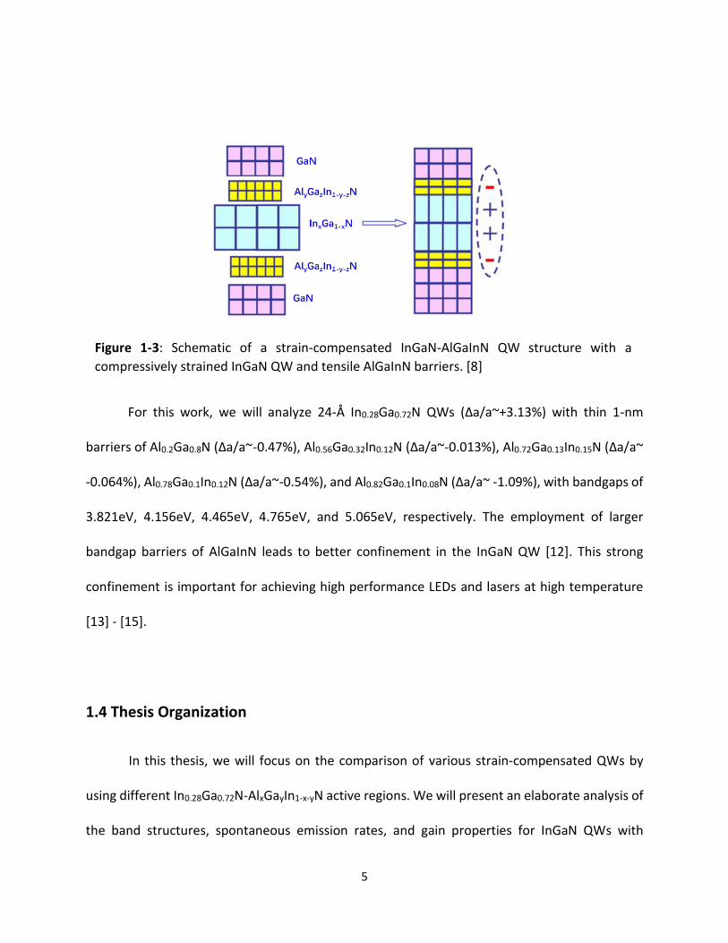
5
Figure 1-3: Schematic of a strain-compensated InGaN-AlGaInN QW structure with a
compressively strained InGaN QW and tensile AlGaInN barriers. [8]
For this work, we will analyze 24-Å In0.28Ga0.72N QWs (∆a/a~+3.13%) with thin 1-nm
barriers of Al0.2Ga0.8N (∆a/a~-0.47%), Al0.56Ga0.32In0.12N (∆a/a~-0.013%), Al0.72Ga0.13In0.15N (∆a/a~
-0.064%), Al0.78Ga0.1In0.12N (∆a/a~-0.54%), and Al0.82Ga0.1In0.08N (∆a/a~ -1.09%), with bandgaps of
3.821eV, 4.156eV, 4.465eV, 4.765eV, and 5.065eV, respectively. The employment of larger
bandgap barriers of AlGaInN leads to better confinement in the InGaN QW [12]. This strong
confinement is important for achieving high performance LEDs and lasers at high temperature
[13] - [15].
1.4 Thesis Organization
In this thesis, we will focus on the comparison of various strain-compensated QWs by
using different In0.28Ga0.72N-AlxGayIn1-x-yN active regions. We will present an elaborate analysis of
the band structures, spontaneous emission rates, and gain properties for InGaN QWs with
6
various AlGaInN barriers. The spontaneous emission and optical gain properties will be calculated
under the self-consistent 6-band k∙p formalism [16], [17]. In Chapter 1, we will begin with an
introduction to InGaN-based semiconductors, their current technological challenges, and the
concept of strain-compensated quantum wells. We will follow this by presenting the 6-band k∙p
method under the self-consistent formalism in Chapter 2. The Chapter 3 will present a
comparison between the band properties of conventional and various strain-compensated
quantum well structures. Finally, in Chapter 4, we will investigate the optical properties of these
conventional and strain-compensated quantum wells. In this thesis, we will limit our comparison
to two classes of active regions, namely: i ) the conventional 24-Å In0.28Ga0.72N-GaN QW and ii)
the strain-compensated 24-Å In0.28Ga0.72N-Al0.2Ga0.8N QW, 24-Å In0.28Ga0.72N-Al0.56Ga0.32In0.12N
QW, and 24-Å In0.28Ga0.72N-Al0.78Ga0.1In0.12N. These results will be presented in Chapters 3 and 4.
7
Chapter 2: Self-Consistent 6-Band k∙p Method for III-Nitride
Semiconductors
In solid-state physics, k∙p perturbation theory is an approximation for the calculation of
band structures and optical properties of crystalline solids [18] near the Γ-point. It is developed
from Bloch theorem. The Bloch equation can be written as the following:
, ,( ) ( )i
n ne u k x
k kx x (2-1)
where k is wave vector, n is the discrete index, and ,nuk
is a function with the same periodicity
as the crystal lattice. This theory is in the framework of the Luttinger-Kohn model. We will present
the concept of 6-band k ∙p method for wurtzite semiconductors, which was developed by
S.L.Chuang et al. [16], [17]. We will also present the formulation of the self-consistent 6-band
k∙p method for III-nitride semiconductor following the framework developed in reference 8.
2.1 The Hamiltonian Matrix Elements for 6-Band k∙p Method
In this thesis, we will utilize the 6-band k∙p method to calculate the band structures of
InGaN-AlGaInN strain-compensated QWs. Our calculation will consider valence band mixing,
strain effect, spontaneous and piezoelectric polarizations, and the carrier screening effect. We
will neglect the coupling between the conduction and valence bands because of the large
bandgap. We will assume the conduction band to be parabolic. The valence band structure will
be calculated via a 6×6 Hamiltonian matrix [17] in the following form:
8
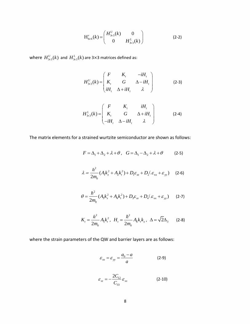
3 3
6 6
3 3
( ) 0H ( )
0 ( )
U
v
L
H kk
H k
(2-2)
where 3 3( )UH k
and 3 3( )LH k
are 3×3 matrices defined as:
3 3( )
t t
U
t t
t t
F K iH
H k K G iH
iH iH
(2-3)
3 3( )
t t
L
t t
t t
F K iH
H k K G iH
iH iH
(2-4)
The matrix elements for a strained wurtzite semiconductor are shown as follows:
1 2F , 1 2G (2-5)
22 2
1 2 1 2 xx
0
( ) )2
z t zz yyAk A k D Dm
( (2-6)
22 2
3 4 3 4 xx
0
( ) )2
z t zz yyA k A k D Dm
( (2-7)
22
5
02t tK A k
m ,
2
6
02t t zH A k k
m , 32 (2-8)
where the strain parameters of the QW and barrier layers are as follows:
0xx yy
a a
a
(2-9)
12
33
2zz xx
C
C (2-10)
9
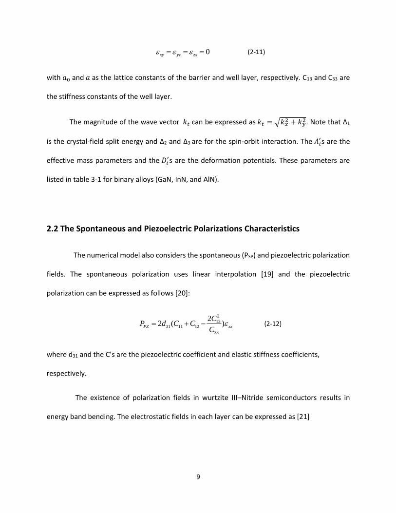
0xy yz zx (2-11)
with 𝑎0 and 𝑎 as the lattice constants of the barrier and well layer, respectively. C13 and C33 are
the stiffness constants of the well layer.
The magnitude of the wave vector 𝑘𝑡 can be expressed as 𝑘𝑡 = √𝑘𝑥2 + 𝑘𝑦2. Note that ∆1
is the crystal-field split energy and ∆2 and ∆3 are for the spin-orbit interaction. The 𝐴𝑖′s are the
effective mass parameters and the 𝐷𝑖′s are the deformation potentials. These parameters are
listed in table 3-1 for binary alloys (GaN, InN, and AlN).
2.2 The Spontaneous and Piezoelectric Polarizations Characteristics
The numerical model also considers the spontaneous (PSP) and piezoelectric polarization
fields. The spontaneous polarization uses linear interpolation [19] and the piezoelectric
polarization can be expressed as follows [20]:
2
1331 11 12
33
22 ( )PZ xx
CP d C C
C (2-12)
where d31 and the C’s are the piezoelectric coefficient and elastic stiffness coefficients,
respectively.
The existence of polarization fields in wurtzite III–Nitride semiconductors results in
energy band bending. The electrostatic fields in each layer can be expressed as [21]
10
/ /
/
k k k j k k
k kj
j k k
k
l P P l
El
(2-13)
where P is the total macroscopic polarization, ε is the static dielectric constant, and 𝑙 is the
thickness of each layers.
For the average electric field in the layers, note that the electric field expression in (2-
13) needs to satisfy the periodic boundary conditions as follows:
0k k
k
l E (2-14)
where the summation consists of all layers, including the QW, active regions, and barrier regions.
Note that the total electric field of each layer is the slope for the band lineups.
2.3 Momentum Matrix Elements and Fermi’s Golden Rule
The optical transition matrix element relating nth-state in conduction band and mth-state
in valence band can be calculated via the envelope functions, as shown below:
• TE-polarization (�̂� or �̂� polarization)
22 (1) 2 (2) 2| | | |
| ( ) ( ) | { | | } for =U4
xx nm t n m n m
S p ZM k g g
(2-15a)
22 (4) 2 (5) 2| | | |
| ( ) ( ) | { | | } for =L4
xx nm t n m n m
S p ZM k g g
(2-15b)
• TM-polarization (�̂� polarization)
11
22 (3) 2| | | |
| ( ) ( ) | | for =U4
zz nm t n m
S p ZM k g
(2-16a)
22 (6) 2| | | |
| ( ) ( ) | | for =L4
zz nm t n m
S p ZM k g
(2-16b)
where ϕ𝑛 and 𝑔𝑚 are the conduction and valence band wave functions, respectively. The upper
and lower Hamiltonian blocks are indicated by σ=U and σ=L, respectively. In our calculation, the
linewidth broadening time (𝜏𝑠) is assumed to have Lorentzian shape with 𝜏𝑠 = 0.1𝑝𝑠.
Based on the Fermi’s Golden Rule, the spontaneous emission rate for TE (e=x) or TM (e=z)
polarizations can be obtained by considering all the transitions between the nth conduction
subbands and mth valence subbands as follows:
22
2 2 2, ,0 0 ,
( )(1 ( ))( / )2qg ( )= | ( ) ( ) |
2 ( ( ) )
c ve t t n t m tsp x nm t cv
U L n mr nm t
k dk f k f kM k
n c m L E k
(2-17)
The optical gains for the TE (𝑔𝑇𝐸 ) and TM (𝑔𝑇𝑀 ) polarizations are related to the
spontaneous emission rate as follows:
( ) g ( )[1 exp( )]TE x
sp
B
Fg
k T
(2-18a)
( ) g ( )[1 exp( )]TM z
sp
B
Fg
k T
(2-18b)
Note that the parameter ∆F is the separation of the quasi-Fermi levels of electrons (𝐹𝑐)
and the holes (𝐹𝑣). The parameter ∆F can be expressed as ∆𝐹 = 𝐹𝑐 − 𝐹𝑣, which depends on the
injection carrier densities (𝑛 and 𝑝) shown as follows:
12
2( )
2
ct tn t
n
k dkn f k
L (2-19)
,
1(1 ( ))
2
vt tm t
U L m
k dkp f k
L
(2-20)
Note that 𝑓𝑛𝑐(𝑘𝑡) and 𝑓𝜎𝑚
𝑣 (𝑘𝑡) are the Fermi-Dirac distribution functions for the
electrons in conduction band and valence band, given as follows:
1( )
( )1 exp( )
c
n t c
n t c
B
f kE k F
k T
(2-21)
,
1( )
( )1 exp( )
v
m t v
m t v
B
f kE k F
k T
(2-22)
For the calculation of the spontaneous emission rate, we consider both TE and TM
polarizations. The total momentum matrix element is the average of two TE-polarization
components and one TM-polarization component [17], which can be expressed as follows:
2 2 21| | (2 | | | | )
3sp x zM M M (2-23)
The spontaneous emission rate (𝑠−1𝑐𝑚−3𝑒𝑉−1) can be written as follows:
2 2
2 2
2(2 )( )
3
x z
sp spspon eg gn
r Ec
(2-24)
The spontaneous emission radiative recombination rate (𝑠−1𝑐𝑚−3 ) is obtained by
integrating (2-24) over the entire frequency range as follows [22]:
13
0
( ) ( )spon
spR r d
(2-25)
2.4 Self-Consistent Schrödinger and Poisson Equations
The calculations of the eigenenergies and wave functions are based on the self-
consistent model of solving the Poisson equation [22] expressed as follows:
( ) ( )scVz
z z
(2-26)
where 𝑉𝑠𝑐 is an intermediate quantity and ρ(z) is the charge distribution given by:
( ) | | [ ( ) ( )]z e p z n z (2-27)
Note that the electron and hole concentrations are related to the wave functions of the
𝑛𝑡ℎ conduction subband 𝜙𝑛(𝑧) and the 𝑚𝑡ℎ valence subband 𝑔𝑚(𝑧). The corresponding surface
electron concentration (𝑁𝑛) and surface hole concentration (𝑃𝑚) are given as follows:
2( ) | ( ) |n n
n
n z z N (2-28)
2( ) | ( ) |m m
n
p z g z P (2-29)
The surface electron concentration in the nth conduction band can be expressed as:
[ ( ) ]/2
0
2 12
(2 ) 1 en t c B
tn tE k F k T
kN dk
e
(2-30)
and the surface hole concentration in the mth valence band is given by:
14
[ ( ) ]/2
0
2 12
(2 ) 1 hm t v B
tm tE k F k T
kP dk
e
(2-31)
The 𝑉𝑠𝑐(𝑧) term will modify both the total potential profiles for electrons, 𝑈𝑒(𝑧), and
holes, 𝑈ℎ(𝑧), as follows:
0( ) ( ) | | ( )e
e scU z U z e V z (2-32)
0( ) ( ) | | ( )h
h scU z U z e V z (2-33)
Thus, the self-consistent Schrödinger equations for the carrier screening effect of
electrons and holes can be expressed as follows:
2 2
* 2[ ( )] ( ) ( )
2e e
e
dU z z E z
m dz (2-34)
2 2
* 2[ ( )] ( ) ( )2
h h
h
dU z g z E g z
m dz (2-35)
Note that 𝑉𝑠𝑐(𝑧), which is proportional to the carrier density n, is the dominant variable
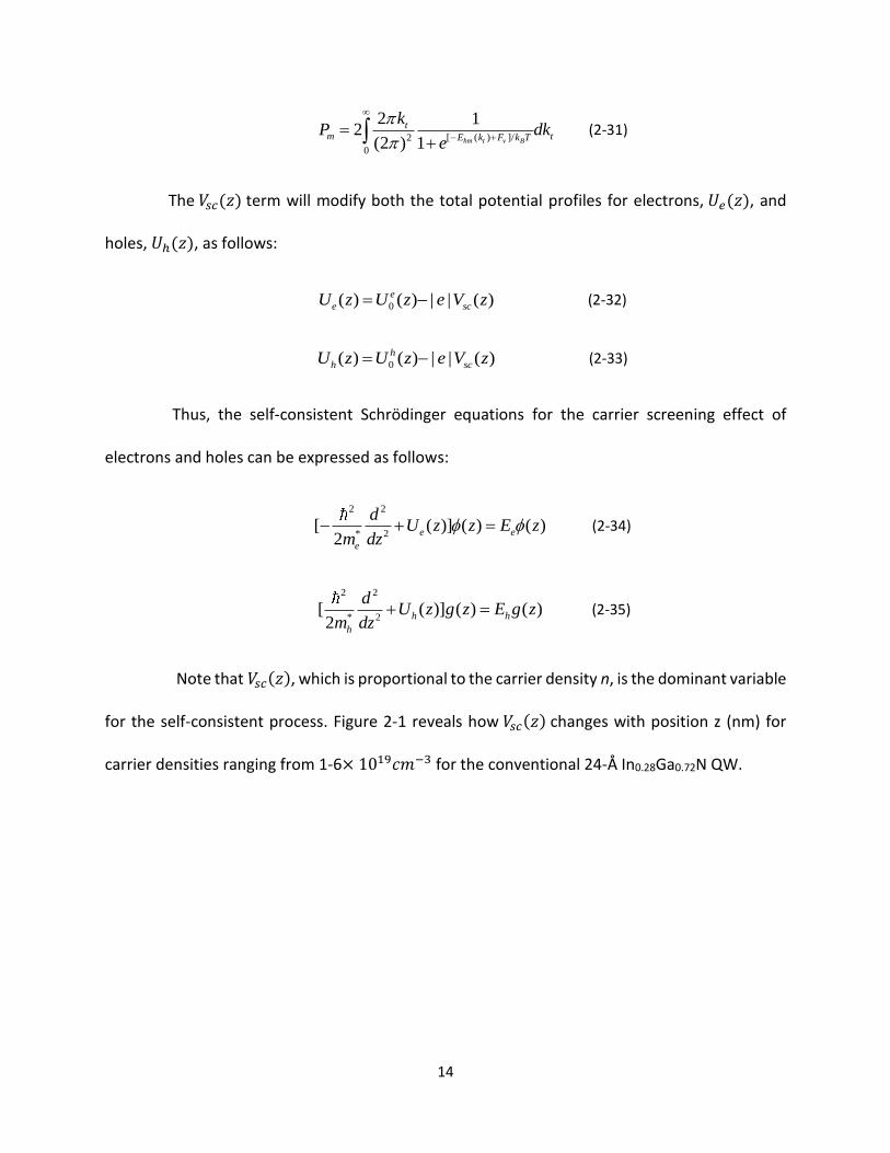
for the self-consistent process. Figure 2-1 reveals how 𝑉𝑠𝑐(𝑧) changes with position z (nm) for
carrier densities ranging from 1-6× 10¹⁹𝑐𝑚−3 for the conventional 24-Å In0.28Ga0.72N QW.

15
Figure 2-1: 𝑉𝑠𝑐(𝑒𝑉) versus position z (nm) for a conventional 24-Å In0.28Ga0.72N QW. The
carrier density n ranges from 1-6× 10¹⁹𝑐𝑚−3 .
2.5 Summary
In this chapter we have presented the Hamiltonian matrix elements, the spontaneous
and piezoelectric polarization equations, momentum matrix elements, and self-consistent
Schrödinger and Poisson equations based upon the 6-band k ∙ p formalism for wurtzite
semiconductors. Under this formalism, we will utilize the finite difference method [23] to solve
the band structures, spontaneous emission rates, and gain properties for InGaN-AlGaInN QWs in
Chapters 3 and 4.
-0.15
-0.1
-0.05
0
0.05
0.1
0.15
0.2
0 2 4 6 8 10 12 14
= − × −
z (nm)
VSC
(eV
)
24-Å In0.28Ga0.72N QW
16
Chapter 3: Band Properties for InGaN-AlGaInN Quantum Wells
In Chapter 2, we have presented the 6-band k∙p formalism for wurtzite semiconductors.
In this chapter, we will present the band lineups, carrier concentration distributions, valence
band structures, and momentum matrix elements characteristics for a conventional 24-Å
In0.28Ga0.72N-GaN QW and strain-compensated 24-Å In0.28Ga0.72N-Al0.2Ga0.8N QW, 24-Å
In0.28Ga0.72N-Al0.56Ga0.32In0.12N QW, and 24-Å In0.28Ga0.72N-Al0.78Ga0.1In0.12N QW. We will analyze
the difference among these QWs.
3.1 Band Lineups and Carrier Concentration Distributions
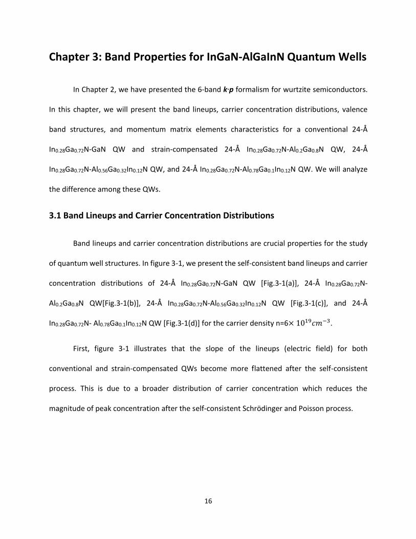
Band lineups and carrier concentration distributions are crucial properties for the study
of quantum well structures. In figure 3-1, we present the self-consistent band lineups and carrier
concentration distributions of 24-Å In0.28Ga0.72N-GaN QW [Fig.3-1(a)], 24-Å In0.28Ga0.72N-
Al0.2Ga0.8N QW[Fig.3-1(b)], 24-Å In0.28Ga0.72N-Al0.56Ga0.32In0.12N QW [Fig.3-1(c)], and 24-Å
In0.28Ga0.72N- Al0.78Ga0.1In0.12N QW [Fig.3-1(d)] for the carrier density n=6× 10¹⁹𝑐𝑚−3.
First, figure 3-1 illustrates that the slope of the lineups (electric field) for both
conventional and strain-compensated QWs become more flattened after the self-consistent
process. This is due to a broader distribution of carrier concentration which reduces the
magnitude of peak concentration after the self-consistent Schrödinger and Poisson process.
17
Figure 3-1: Self-consistent band lineups and carrier concentration distributions of (a) 24-Å
In0.28Ga0.72N-GaN QW, (b) 24-Å In0.28Ga0.72N-Al0.2Ga0.8N QW, (c) 24-Å In0.28Ga0.72N-Al0.56Ga0.32In0.12N
QW, and (d) 24-Å In0.28Ga0.72N-Al0.78Ga0.1In0.12N QW for carrier density n=6× 10¹⁹𝑐𝑚−3.
Second, figure 3-1 illustrates that for both conventional and strain-compensated QWs,
the hole concentration distributions are narrower than the electron concentration distributions.
This is because the concentration is proportional to the wave function distribution, which is
calculated by the Schrödinger equation. We know that the electron effective mass is much
smaller than the hole effective mass, so the wave function distribution calculated by the
Schrödinger equation for electrons will appear broader than that of the holes.
-1
0
1
2
3
4
5
0 2 4 6 8 10 12 14
En
erg
y (
eV
)
without self-consistentwith self-consistent
Ec
Ev
z (nm)
24Å In0.28Ga0.72N
GaNGaN
-1
0
1
2
3
4
5
0 2 4 6 8 10 12 14
En
erg
y (
eV
)
without self-consistentwith self-consistent
Ec
Ev
z (nm)
24Å In0.28Ga0.72N
GaNGaN
1-nm Al0.2Ga0.8N
-1
0
1
2
3
4
5
0 2 4 6 8 10 12 14
En
erg
y (
eV
)
without self-consistentwith self-consistent
Ec
Ev
z (nm)
24Å In0.28Ga0.72N
GaNGaN
1-nm Al0.56Ga0.32In0.12N
-2
-1
0
1
2
3
4
5
6
0 2 4 6 8 10 12 14
En
erg
y (
eV
)
without self-consistentwith self-consistent
Ec
Ev
z (nm)
24Å In0.28Ga0.72N
GaN GaN
1-nm Al0.78Ga0.1In0.12N
(a) (b)
(c) (d)

18
Third, compared to the conventional QW, the strain-compensated QWs have a higher
confinement potential for InGaN QW. This improved confinement results in better optical
properties. We will detail the analysis in Chapter 4.
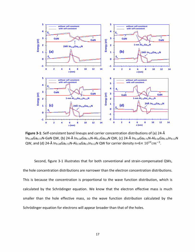
3.2 Valence Band Structures
The valence band structures of both the conventional InGaN–GaN QW and the strain-
compensated QWs are calculated from (2-2) - (2-14), using the parameters of GaN, InN, and AlN
shown in table 3-1 [21]. The bowing parameters used to calculate the bandgaps for InGaN, AlGaN
and AlInN are 1.4 eV, 0.8 eV and 2.74 eV, respectively. Other parameters for AlGaInN use linear
interpolation of the binary alloy (InN, GaN, AlN) parameters.
In figure 3-2, the shape of the band-edge structures for both conventional and the strain-
compensated QWs are very similar, which suggests they have similar effective masses. However,
there are some important differences to emphasize.
First, compared to the conventional QW, the HH1 and LH1 subbands of the strain-
compensated QWs shift up about 0.02eV (b), 0.01ev (c) and 0.015eV (d), respectively.
Second, the separations of the subband energy levels (HH1, LH1 & HH2, LH2) increases in
general, as the barrier bandgap increases. This can be attributed to the stronger quantum
confinement effect from the larger band offsets between the barrier and QW in the case of strain-
compensated InGaN-AlGaInN system.
19
Figure 3-2: Valence band structures for the (a) 24-Å In0.28Ga0.72N-GaN QW (b) 24-Å
In0.28Ga0.72N-Al0.2Ga0.8N QW, (c) 24-Å In0.28Ga0.72N-Al0.56Ga0.32In0.12N QW, and (d) 24-Å
In0.28Ga0.72N-Al0.78Ga0.1In0.12N QW for the carrier density n=6× 10¹⁹𝑐𝑚−3..
Finally, note that the valence subbands will not cross one another. Whenever they trend
to a crossing, the two subbands seem to repel away from one another and exchange their wave
functions. This phenomenon is called valence band mixing.
20
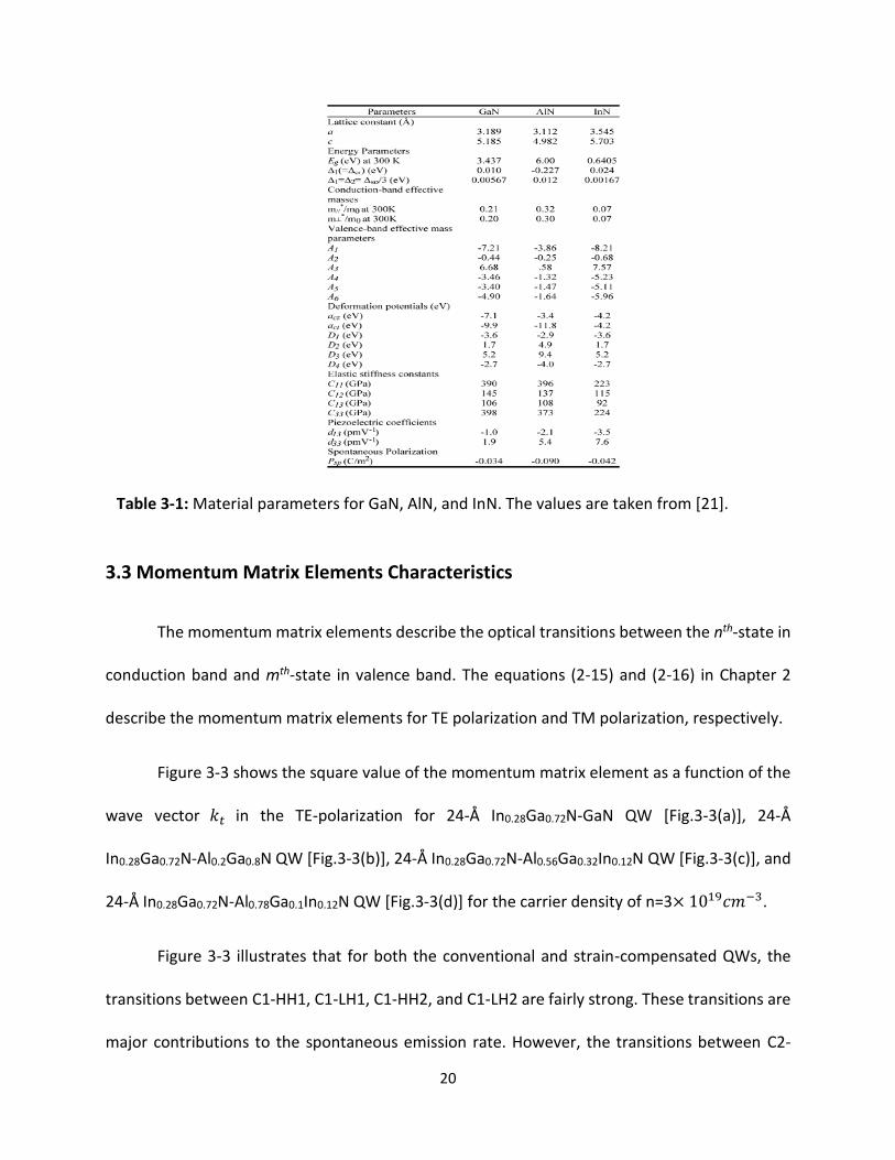
Table 3-1: Material parameters for GaN, AlN, and InN. The values are taken from [21].
3.3 Momentum Matrix Elements Characteristics
The momentum matrix elements describe the optical transitions between the nth-state in
conduction band and mth-state in valence band. The equations (2-15) and (2-16) in Chapter 2
describe the momentum matrix elements for TE polarization and TM polarization, respectively.
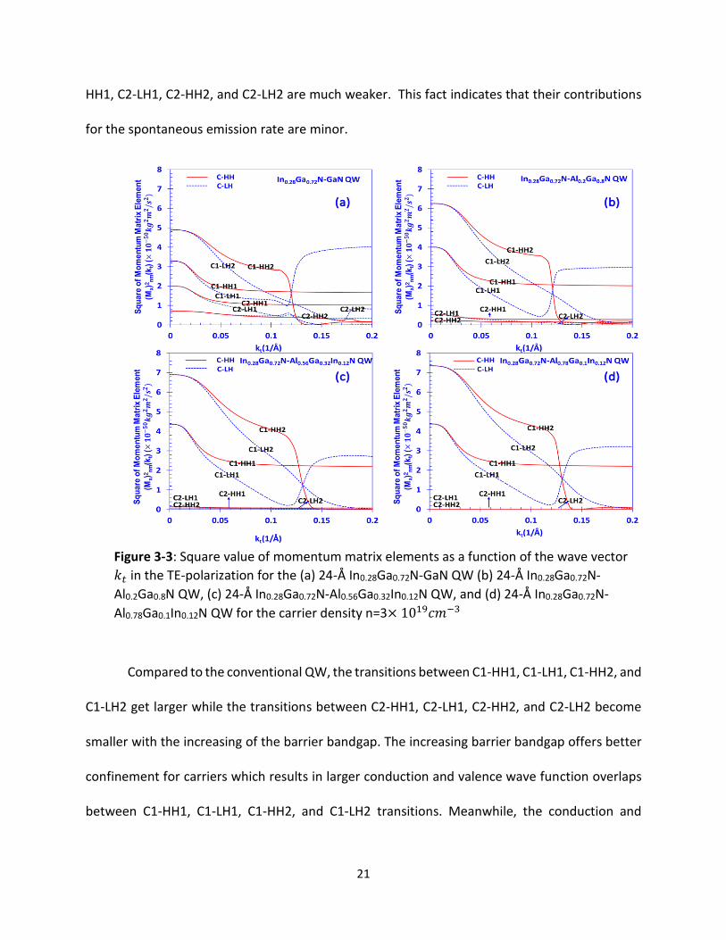
Figure 3-3 shows the square value of the momentum matrix element as a function of the
wave vector 𝑘𝑡 in the TE-polarization for 24-Å In0.28Ga0.72N-GaN QW [Fig.3-3(a)], 24-Å
In0.28Ga0.72N-Al0.2Ga0.8N QW [Fig.3-3(b)], 24-Å In0.28Ga0.72N-Al0.56Ga0.32In0.12N QW [Fig.3-3(c)], and
24-Å In0.28Ga0.72N-Al0.78Ga0.1In0.12N QW [Fig.3-3(d)] for the carrier density of n=3× 10¹⁹𝑐𝑚−3.
Figure 3-3 illustrates that for both the conventional and strain-compensated QWs, the
transitions between C1-HH1, C1-LH1, C1-HH2, and C1-LH2 are fairly strong. These transitions are
major contributions to the spontaneous emission rate. However, the transitions between C2-
21
Figure 3-3: Square value of momentum matrix elements as a function of the wave vector
𝑘𝑡 in the TE-polarization for the (a) 24-Å In0.28Ga0.72N-GaN QW (b) 24-Å In0.28Ga0.72N-
Al0.2Ga0.8N QW, (c) 24-Å In0.28Ga0.72N-Al0.56Ga0.32In0.12N QW, and (d) 24-Å In0.28Ga0.72N-
Al0.78Ga0.1In0.12N QW for the carrier density n=3× 10¹⁹𝑐𝑚−3
HH1, C2-LH1, C2-HH2, and C2-LH2 are much weaker. This fact indicates that their contributions
for the spontaneous emission rate are minor.
Compared to the conventional QW, the transitions between C1-HH1, C1-LH1, C1-HH2, and
C1-LH2 get larger while the transitions between C2-HH1, C2-LH1, C2-HH2, and C2-LH2 become
smaller with the increasing of the barrier bandgap. The increasing barrier bandgap offers better
confinement for carriers which results in larger conduction and valence wave function overlaps
between C1-HH1, C1-LH1, C1-HH2, and C1-LH2 transitions. Meanwhile, the conduction and
(a) (b)
(c) (d)
22
Figure 3-4: Square value of momentum matrix elements at zone center (𝑘𝑡=0) using the self-
consistent model as a function of the carrier density for the (a) 24-Å In0.28Ga0.72N-GaN QW (b)
24-Å In0.28Ga0.72N-Al0.2Ga0.8N QW, (c) 24-Å In0.28Ga0.72N-Al0.56Ga0.32In0.12N QW, and (d) 24-Å
In0.28Ga0.72N-Al0.78Ga0.1In0.12N QW.
valence band overlaps for C2-HH1, C2-LH1, C2-HH2, and C2-LH2 reduce because the band
dispersion gets larger as the barrier bandgap increases (explained in Section 3.2).
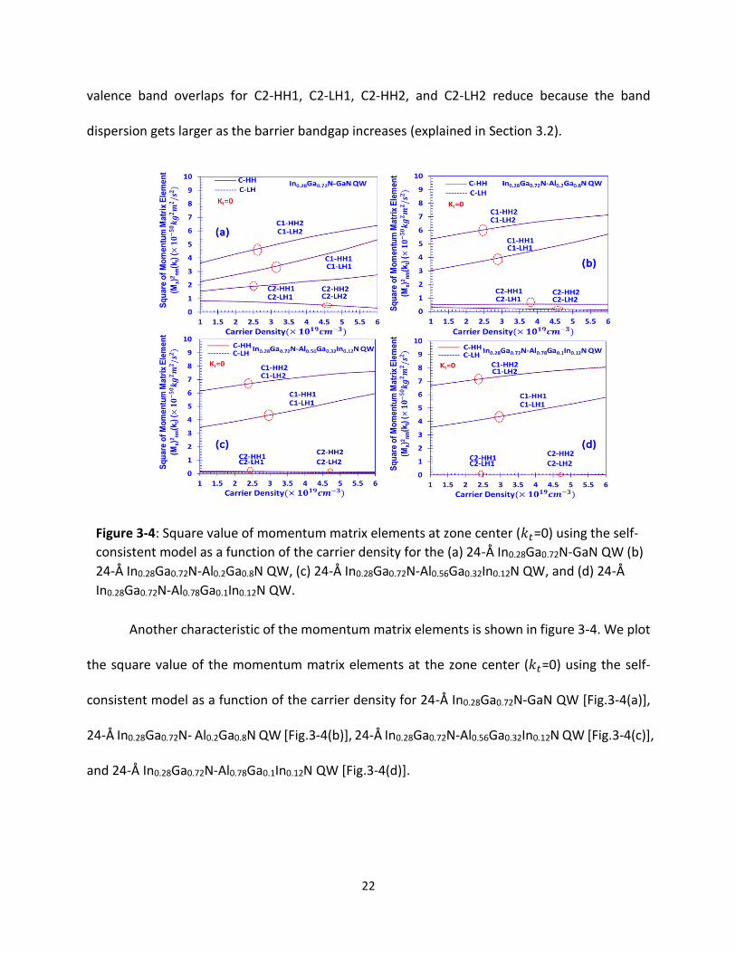
Another characteristic of the momentum matrix elements is shown in figure 3-4. We plot
the square value of the momentum matrix elements at the zone center (𝑘𝑡=0) using the self-
consistent model as a function of the carrier density for 24-Å In0.28Ga0.72N-GaN QW [Fig.3-4(a)],
24-Å In0.28Ga0.72N- Al0.2Ga0.8N QW [Fig.3-4(b)], 24-Å In0.28Ga0.72N-Al0.56Ga0.32In0.12N QW [Fig.3-4(c)],
and 24-Å In0.28Ga0.72N-Al0.78Ga0.1In0.12N QW [Fig.3-4(d)].
(a)
(b)
(c) (d)
23
Figure 3-4 illustrates that both the conventional and strain-compensated QWs indicate an
increasing value of the momentum matrix elements with increasing carrier density for transitions
between C1-HH1, C1-LH1, C1-HH2, and C1-LH2.
Compared to the conventional QW, the square value of the momentum matrix elements
for the C1-HH1, C1-LH1, C1-HH2, and C1-LH2 transitions gets larger with increasing barrier
bandgap for strain-compensated QWs. Increasing the barrier bandgap results in better
confinement in the QWs, which increases the conduction band and valence band wave function
overlaps. We know from figure 3-4 that as the carrier density increases, the square value of the
momentum matrix elements of C2-HH1, C2-LH1, C2-HH2, and C2-LH2 becomes negligible.
3.4 Summary
We present comprehensive analysis of band lineups, carrier concentration distributions,
valence band structures, and momentum matrix elements characteristics for the conventional
24-Å In0.28Ga0.72N-GaN QW and strain-compensated 24-Å In0.28Ga0.72N-Al0.2Ga0.8N QW, 24-Å
In0.28Ga0.72N-Al0.56Ga0.32In0.12N QW, and 24-Å In0.28Ga0.72N-Al0.78Ga0.1In0.12N QW in this chapter.
We have compared and explained the differences in band properties between conventional and
strain-compensated QWs in this chapter.
24
Chapter 4: Optical Properties of InGaN-AlGaInN Quantum Wells
The optical properties, such as spontaneous emission and gain characteristics, are key
metrics for active region design in LEDs and lasers devices. We have presented a thorough
analysis of the band properties for conventional and strain-compensated QWs in Chapter 3. In
this chapter, we will discuss the spontaneous emission spectra and gain properties for
conventional and strain-compensated QWs.
4.1 Spontaneous Emission Characteristics
Based on the self-consistent 6-band k∙p formalism discussed in Chapter 2, we calculate
the spontaneous emission spectra for 24-Å In0.28Ga0.72N-GaN QW , 24-Å In0.28Ga0.72N-Al0.2Ga0.8N
QW ,24-Å In0.28Ga0.72N-Al0.56Ga0.32In0.12N QW, and 24-Å In0.28Ga0.72N-Al0.78Ga0.1In0.12N QW, with
carrier densities ranging from n=5× 10¹⁸𝑐𝑚−3 up to n=6× 10¹⁹𝑐𝑚−3 at T=300K. We plot the
strain-compensated QWs (red solid line) with conventional QW (blue dotted line) in each figure
for comparison. We divide this into two figures, Fig.4-1 and Fig.4-2, with carrier densities ranging
from n=5× 10¹⁸𝑐𝑚−3 up to n=10× 1018𝑐𝑚−3 and n=2× 10¹⁹𝑐𝑚−3 up to n=6× 10¹⁹𝑐𝑚−3 ,
respectively.
Figure 4-1 illustrates that the spontaneous emission rate for the strain-compensated
QWs is much larger compared to the conventional QW in the low carrier density regime. The
enhancements of the spontaneous emission rate for 24-Å In0.28Ga0.72N-Al0.2Ga0.8N QW, 24-Å
In0.28Ga0.72N-Al0.56Ga0.32In0.12N QW, and 24-Å In0.28Ga0.72N-Al0.78Ga0.1In0.12N QW for the carrier
density n=10× 1018𝑐𝑚−3are 44.4%, 66.7%, and 61.1%, respectively.
25
Figure 4-1: Spontaneous emission spectra comparison of (a) 24-Å In0.28Ga0.72N-Al0.2Ga0.8N QW
and conventional 24-Å In0.28Ga0.72N-GaN QW (b) 24-Å In0.28Ga0.72N-Al0.56Ga0.32In0.12N QW and
conventional 24-Å In0.28Ga0.72N-GaN QW (c) 24-Å In0.28Ga0.72N-Al0.78Ga0.1In0.12N QW and
conventional 24-Å In0.28Ga0.72N-GaN QW. The carrier densities range from n=5× 10¹⁸𝑐𝑚−3
up to n=10× 1018𝑐𝑚−3.
Figure 4-2 demonstrates that the spontaneous emission rate for strain-compensated QWs
is larger than that of the conventional QW in the high carrier density regime. However, the
percentage of enhancement is less than that in the low carrier density range. The enhancements
of the spontaneous emission rate for 24-Å In0.28Ga0.72N-Al0.2Ga0.8N QW, 24-Å In0.28Ga0.72N-
Al0.56Ga0.32In0.12N QW, and 24-Å In0.28Ga0.72N-Al0.78Ga0.1In0.12N QW n=6× 10¹⁹𝑐𝑚−3 are 6.8%,
14.1%, and 8.2%, respectively.
0
0.02
0.04
0.06
0.08
0.1
0.12
0.14
0.16
0.18
2.3 2.35 2.4 2.45 2.5 2.55 2.6
In0.28Ga0.72N-GaN QW
Photon Energy (eV)
Spo
ntan
eous
em
issi
on s
pect
rum
In0.28Ga0.72N-Al0.78Ga0.1In12N QW
n=5-10× −
(a) (b)
0
0.02
0.04
0.06
0.08
0.1
0.12
0.14
0.16
0.18
2.3 2.35 2.4 2.45 2.5 2.55 2.6
In0.28Ga0.72N-GaN QW
Photon Energy (eV)
Spo
ntan
eous
em
issi
on s
pect
rum
In0.28Ga0.72N-Al0.56Ga0.32In0.12N QW
n=5-10× −
(c)
26
Figure 4-2: Spontaneous emission spectra comparison of (a) 24-Å In0.28Ga0.72N-Al0.2Ga0.8N QW
and conventional 24-Å In0.28Ga0.72N-GaN QW (b) 24-Å In0.28Ga0.72N-Al0.56Ga0.32In0.12N QW and
conventional 24-Å In0.28Ga0.72N-GaN QW (c) 24-Å In0.28Ga0.72N-Al0.78Ga0.1In0.12N QW and
conventional 24-Å In0.28Ga0.72N-GaN QW. The carrier densities range from n=2× 10¹⁹𝑐𝑚−3
up to n=6× 10¹⁹𝑐𝑚−3.
From both figures 4-1 and 4-2, we observe a blue shift in strain-compensated 24-Å
In0.28Ga0.72N-Al0.2Ga0.8N QW, 24-Å In0.28Ga0.72N-Al0.56Ga0.32In0.12N QW, and 24-Å In0.28Ga0.72N-
Al0.78Ga0.1In0.12N QW compared to the conventional QW. This is due to the larger band dispersion
from the increased barrier bandgap, as discussed in Section 3.2.
For laser operation, the typical threshold carrier density of InGaN QW ranges from 𝑛 =
3.5 × 10¹⁹𝑐𝑚−3 to 𝑛 = 7 × 10¹⁹𝑐𝑚−3 [24]. For the case of 𝑛 = 3 × 10¹⁹𝑐𝑚−3 ( 𝑛 = 5 ×
0
0.5
1
1.5
2
2.5
3
2.4 2.5 2.6 2.7 2.8 2.9 3
n=2-6× − Sp
ont
aneo
us e
mis
sion
spe
ctru
m
Photon Energy (eV)
In0.28Ga0.72N-Al0.78Ga0.1In0.12N QW
In0.28Ga0.72N-GaN QWIn0.28Ga0.72N-Al0.2Ga0.8N QW
0
0.5
1
1.5
2
2.5
3
2.4 2.5 2.6 2.7 2.8 2.9 3
n=2-6× −
Spo
ntan
eous
em
issi
on s
pect
rum
Photon Energy (eV)
In0.28Ga0.72N-Al0.78Ga0.1In0.12N QW
In0.28Ga0.72N-GaN QWIn0.28Ga0.72N-Al0.56Ga0.32In0.12N QW
0
0.5
1
1.5
2
2.5
3
2.4 2.5 2.6 2.7 2.8 2.9 3
n=2-6× −
Spo
ntan
eous
em
issi
on s
pect
rum
Photon Energy (eV)
In0.28Ga0.72N-Al0.78Ga0.1In0.12N QW
In0.28Ga0.72N-GaN QW
(a) (b)
(c)
27
Table 4-1: Enhancement factors of the spontaneous emission rate for strain-compensated 24-
Å In0.28Ga0.72N- Al0.2Ga0.8N QW, 24-Å In0.28Ga0.72N-Al0.56Ga0.32In0.12N QW, and 24-Å
In0.28Ga0.72N-Al0.78Ga0.1In0.12N QW compared to conventional 24-Å In0.28Ga0.72N-GaN QW at
transparency(n=3× 10¹⁹𝑐𝑚−3) and near threshold (n=5× 10¹⁹𝑐𝑚−3).
1019𝑐𝑚−3), the strain-compensated InGaN QW structures exhibit enhancement factors as given
in table 4-1.
In figure 4-3, we plot the peak value of spontaneous emission rate versus increasing
barrier bandgap (eV) for 24-Å In0.28Ga0.72N-GaN (3.437eV) QW, 24-Å In0.28Ga0.72N- Al0.2Ga0.8N
(3.822eV) QW, 24-Å In0.28Ga0.72N-Al0.56Ga0.32In0.12N (4.156 eV) QW, 24-Å In0.28Ga0.72N-
Al0.72Ga0.13In0.15N (4.465eV) QW, 24-Å In0.28Ga0.72N-Al0.78Ga0.1In0.12N (4.765eV) QW, and 24-Å
In0.28Ga0.72N-Al0.82Ga0.1In0.08N (5.065eV) QW. The carrier density is calculated at n=6× 10¹⁹𝑐𝑚−3.
The figure shows a parabolic shape for barrier bandgaps from 3.43eV-5.06eV, which indicates
that one can obtain an optimized 1-nm strain compensated barrier for 24-Å In0.28Ga0.72N-AlGaInN
QW between bandgaps of 4.2eV and 4.4eV which provides best spontaneous emission properties.
Note that the figure is plotted for a carrier density n=6× 10¹⁹𝑐𝑚−3 only for illustrative purposes.
GaN Al0.2Ga0.8N Al0.56Ga0.32In0.12N Al0.78Ga0.1In0.12N
Latticeconstant (Å )
3.1890 3.1736 3.1886 3.1717
Bandgap (eV) 3.437 3.822 4.156 4.765
Enhancementfactor (n=3× − )
100% 122% 135% 132%
Enhancementfactor (n=5×
− )
100% 112% 119% 116%
28
Figure 4-3: Peak value of spontaneous emission rate versus increasing barrier bandgap (eV)
for 24-Å In0.28Ga0.72N-GaN QW (3.437eV), 24-Å In0.28Ga0.72N-Al0.2Ga0.8N QW (3.822eV), 24-Å
In0.28Ga0.72N-Al0.56Ga0.32In0.12N QW (4.156eV), 24-Å In0.28Ga0.72N-Al0.72Ga0.13In0.15N QW
(4.465eV), 24-Å In0.28Ga0.72N-Al0.78Ga0.1In0.12N QW (4.765eV), and 24-Å In0.28Ga0.72N-
Al0.82Ga0.1In0.08N QW (5.065eV). The carrier density is calculated at n=6× 10¹⁹𝑐𝑚−3.
In fact, we get similar results for all calculated carrier densities ranging from n=1 ×
1018𝑐𝑚−3 up to n = 6 × 10¹⁹𝑐𝑚−3 .
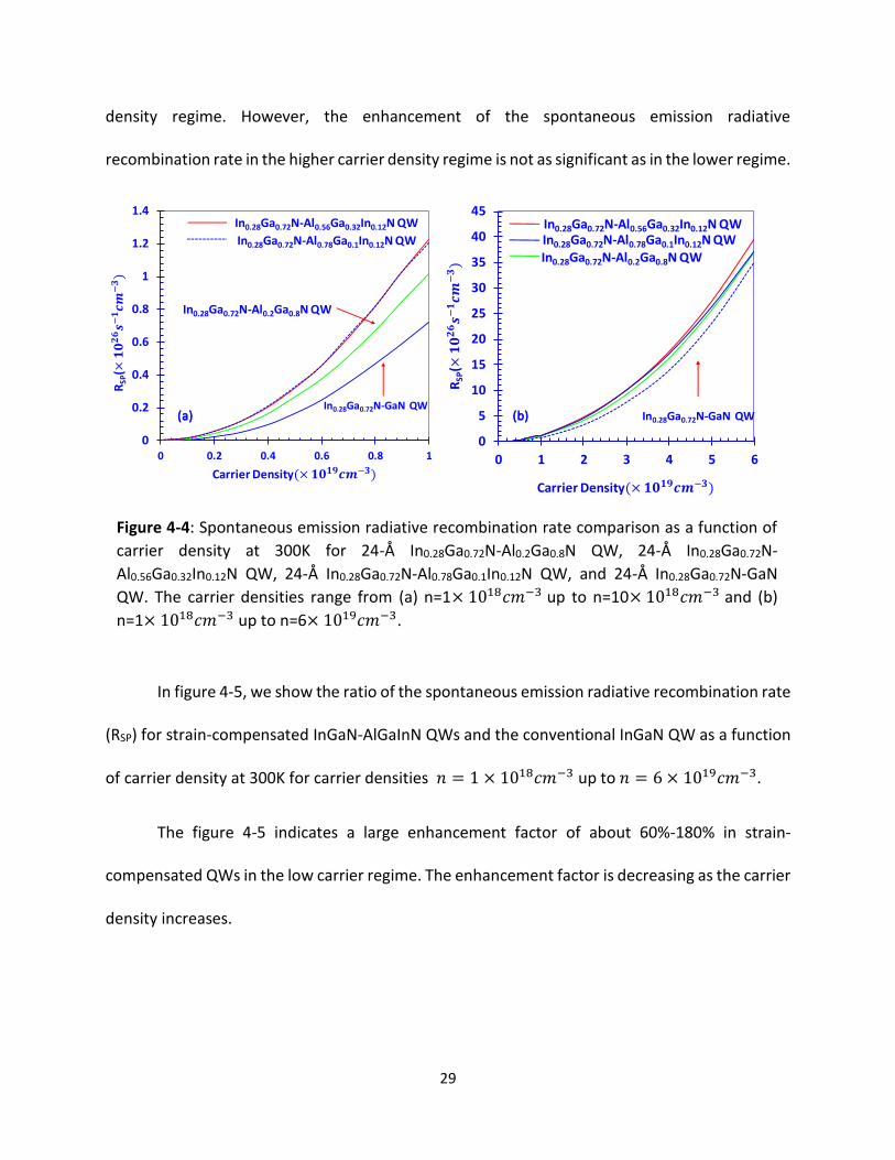
In figure 4-4, the spontaneous emission radiative recombination rate (RSP) of the strain-
compensated In0.28Ga0.72N–Al0.2Ga0.8N QW, In0.28Ga0.72N–Al0.56Ga0.32In0.12N QW, and
In0.28Ga0.72N–Al0.78Ga0.1In0.12N QW and conventional In0.28Ga0.72N–GaN QW are plotted against
carrier density (n), in the low carrier density regime (from 𝑛 = 1 × 10¹⁸𝑐𝑚−3 up to 𝑛 =
10 × 1018𝑐𝑚−3) [Fig.5-4(a)] and the high carrier density regime (from 𝑛 = 2 × 10¹⁹𝑐𝑚−3 up to
𝑛 = 6 × 10¹⁹𝑐𝑚−3 ) [Fig.5-4(b)], respectively. The spontaneous emission radiative
recombination rate can be obtained from (2-25).
Figure 4-4 illustrates that the spontaneous emission radiative recombination rate for
strain-compensated QWs is much higher compared to the conventional QW in the low carrier
29
Figure 4-4: Spontaneous emission radiative recombination rate comparison as a function of
carrier density at 300K for 24-Å In0.28Ga0.72N-Al0.2Ga0.8N QW, 24-Å In0.28Ga0.72N-
Al0.56Ga0.32In0.12N QW, 24-Å In0.28Ga0.72N-Al0.78Ga0.1In0.12N QW, and 24-Å In0.28Ga0.72N-GaN
QW. The carrier densities range from (a) n=1× 10¹⁸𝑐𝑚−3 up to n=10× 1018𝑐𝑚−3 and (b)
n=1× 10¹⁸𝑐𝑚−3 up to n=6× 10¹⁹𝑐𝑚−3.
density regime. However, the enhancement of the spontaneous emission radiative
recombination rate in the higher carrier density regime is not as significant as in the lower regime.
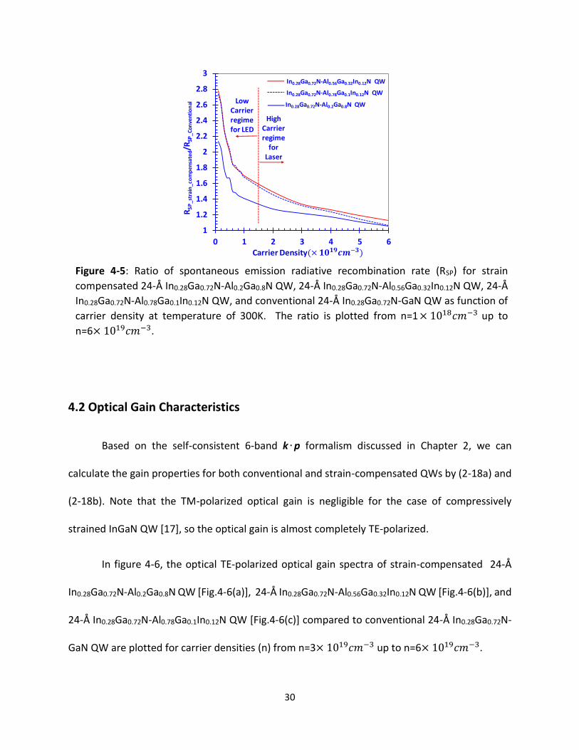
In figure 4-5, we show the ratio of the spontaneous emission radiative recombination rate
(RSP) for strain-compensated InGaN-AlGaInN QWs and the conventional InGaN QW as a function
of carrier density at 300K for carrier densities 𝑛 = 1 × 10¹⁸𝑐𝑚−3 up to 𝑛 = 6 × 10¹⁹𝑐𝑚−3.
The figure 4-5 indicates a large enhancement factor of about 60%-180% in strain-
compensated QWs in the low carrier regime. The enhancement factor is decreasing as the carrier
density increases.
0
0.2
0.4
0.6
0.8
1
1.2
1.4
0 0.2 0.4 0.6 0.8 1
Carrier Density(× − )
RSP
(
In0.28Ga0.72N-GaN QW
In0.28Ga0.72N-Al0.56Ga0.32In0.12N QW
In0.28Ga0.72N-Al0.2Ga0.8N QW
In0.28Ga0.72N-Al0.78Ga0.1In0.12N QW
0
5
10
15
20
25
30
35
40
45
0 1 2 3 4 5 6
Carrier Density(× − )
RSP
(
In0.28Ga0.72N-GaN QW
In0.28Ga0.72N-Al0.56Ga0.32In0.12N QWIn0.28Ga0.72N-Al0.78Ga0.1In0.12N QWIn0.28Ga0.72N-Al0.2Ga0.8N QW
(a) (b)
30
Figure 4-5: Ratio of spontaneous emission radiative recombination rate (RSP) for strain
compensated 24-Å In0.28Ga0.72N-Al0.2Ga0.8N QW, 24-Å In0.28Ga0.72N-Al0.56Ga0.32In0.12N QW, 24-Å
In0.28Ga0.72N-Al0.78Ga0.1In0.12N QW, and conventional 24-Å In0.28Ga0.72N-GaN QW as function of
carrier density at temperature of 300K. The ratio is plotted from n=1× 10¹⁸𝑐𝑚−3 up to
n=6× 10¹⁹𝑐𝑚−3.
4.2 Optical Gain Characteristics
Based on the self-consistent 6-band k ∙p formalism discussed in Chapter 2, we can
calculate the gain properties for both conventional and strain-compensated QWs by (2-18a) and
(2-18b). Note that the TM-polarized optical gain is negligible for the case of compressively
strained InGaN QW [17], so the optical gain is almost completely TE-polarized.
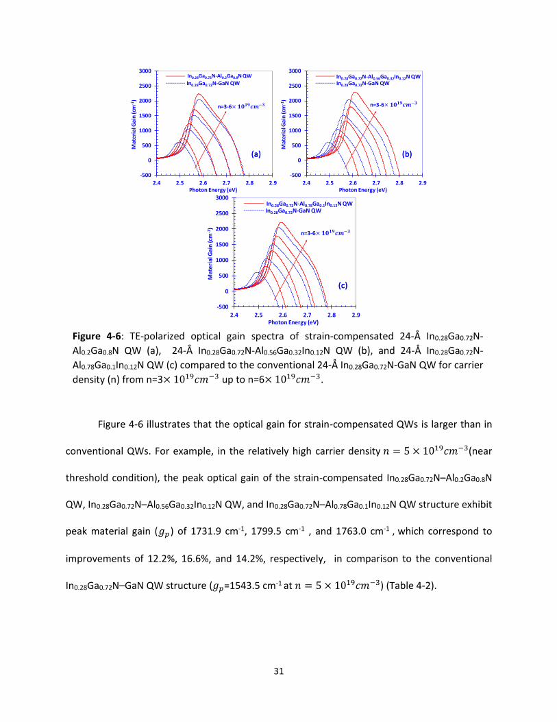
In figure 4-6, the optical TE-polarized optical gain spectra of strain-compensated 24-Å
In0.28Ga0.72N-Al0.2Ga0.8N QW [Fig.4-6(a)], 24-Å In0.28Ga0.72N-Al0.56Ga0.32In0.12N QW [Fig.4-6(b)], and
24-Å In0.28Ga0.72N-Al0.78Ga0.1In0.12N QW [Fig.4-6(c)] compared to conventional 24-Å In0.28Ga0.72N-
GaN QW are plotted for carrier densities (n) from n=3× 10¹⁹𝑐𝑚−3 up to n=6× 10¹⁹𝑐𝑚−3.
1
1.2
1.4
1.6
1.8
2
2.2
2.4
2.6
2.8
3
0 1 2 3 4 5 6Carrier Density(× − )
RS
P_s
tra
in_c
om
pe
nsa
ted/R
SP_C
onve
ntio
nal Low
Carrier regime for LED
High Carrier regime
for Laser
In0.28Ga0.72N-Al0.56Ga0.32In0.12N QW
In0.28Ga0.72N-Al0.78Ga0.1In0.12N QW
In0.28Ga0.72N-Al0.2Ga0.8N QW
31
Figure 4-6: TE-polarized optical gain spectra of strain-compensated 24-Å In0.28Ga0.72N-
Al0.2Ga0.8N QW (a), 24-Å In0.28Ga0.72N-Al0.56Ga0.32In0.12N QW (b), and 24-Å In0.28Ga0.72N-
Al0.78Ga0.1In0.12N QW (c) compared to the conventional 24-Å In0.28Ga0.72N-GaN QW for carrier
density (n) from n=3× 10¹⁹𝑐𝑚−3 up to n=6× 10¹⁹𝑐𝑚−3.
Figure 4-6 illustrates that the optical gain for strain-compensated QWs is larger than in
conventional QWs. For example, in the relatively high carrier density 𝑛 = 5 × 10¹⁹𝑐𝑚−3(near
threshold condition), the peak optical gain of the strain-compensated In0.28Ga0.72N–Al0.2Ga0.8N
QW, In0.28Ga0.72N–Al0.56Ga0.32In0.12N QW, and In0.28Ga0.72N–Al0.78Ga0.1In0.12N QW structure exhibit
peak material gain (𝑔𝑝) of 1731.9 cm-1, 1799.5 cm-1 , and 1763.0 cm-1 , which correspond to
improvements of 12.2%, 16.6%, and 14.2%, respectively, in comparison to the conventional
In0.28Ga0.72N–GaN QW structure (𝑔𝑝=1543.5 cm-1 at 𝑛 = 5 × 10¹⁹𝑐𝑚−3) (Table 4-2).
-500
0
500
1000
1500
2000
2500
3000
2.4 2.5 2.6 2.7 2.8 2.9
Mat
eri
al G
ain
(cm
-1)
Photon Energy (eV)
In0.28Ga0.72N-Al0.78Ga0.1In0.12N QW
n=3-6× −
In0.28Ga0.72N-GaN QWIn0.28Ga0.72N-Al0.2Ga0.8N QW
-500
0
500
1000
1500
2000
2500
3000
2.4 2.5 2.6 2.7 2.8 2.9
Mat
eri
al G
ain
(cm
-1)
Photon Energy (eV)
In0.28Ga0.72N-Al0.56Ga0.32In0.12N QW
n=3-6× −
In0.28Ga0.72N-GaN QW
-500
0
500
1000
1500
2000
2500
3000
2.4 2.5 2.6 2.7 2.8 2.9
Mat
eri
al G
ain
(cm
-1)
Photon Energy (eV)
In0.28Ga0.72N-Al0.78Ga0.1In0.12N QW
n=3-6× −
In0.28Ga0.72N-GaN QW
(a) (b)
(c)
32
Figure 4-7: Peak material gain as a function of carrier density at 300 K for 24-Å In0.28Ga0.72N-
Al0.2Ga0.8N QW, 24-Å In0.28Ga0.72N-Al0.56Ga0.32In0.12N QW, 24-Å In0.28Ga0.72N-Al0.78Ga0.1In0.12N
QW, and 24-Å In0.28Ga0.72N-GaN QW for carrier densities range from n=1× 10¹⁸𝑐𝑚−3 up to
n=6× 10¹⁹𝑐𝑚−3.
Table 4-2: Material gain and enhancement factors for 24-Å In0.28Ga0.72N-Al0.2Ga0.8N QW, 24-Å
In0.28Ga0.72N-Al0.56Ga0.32In0.12N QW, and 24-Å In0.28Ga0.72N-Al0.78Ga0.1In0.12N QW compared to
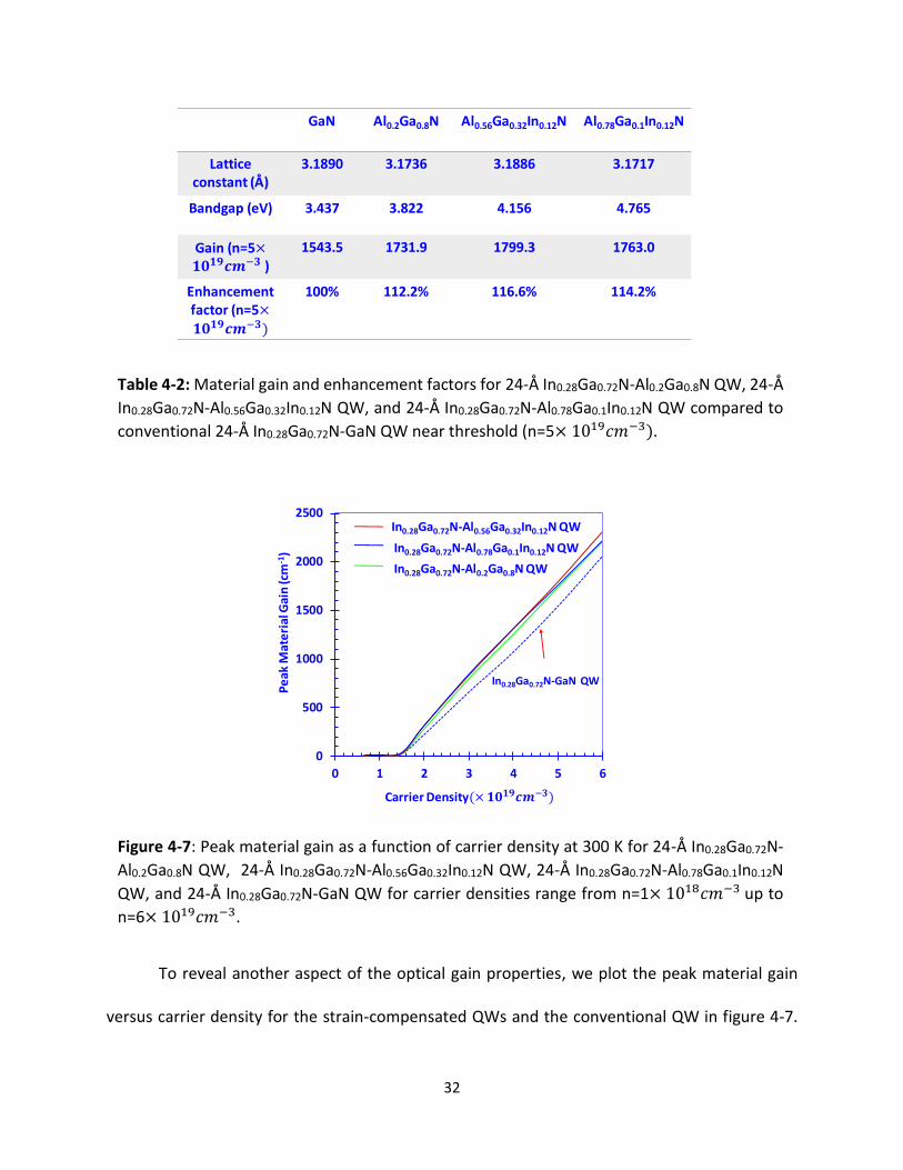
conventional 24-Å In0.28Ga0.72N-GaN QW near threshold (n=5× 10¹⁹𝑐𝑚−3).
To reveal another aspect of the optical gain properties, we plot the peak material gain
versus carrier density for the strain-compensated QWs and the conventional QW in figure 4-7.
GaN Al0.2Ga0.8N Al0.56Ga0.32In0.12N Al0.78Ga0.1In0.12N
Latticeconstant (Å )
3.1890 3.1736 3.1886 3.1717
Bandgap (eV) 3.437 3.822 4.156 4.765
Gain (n=5× − )
1543.5 1731.9 1799.3 1763.0
Enhancementfactor (n=5×
− )
100% 112.2% 116.6% 114.2%
0
500
1000
1500
2000
2500
0 1 2 3 4 5 6
Pe
ak M
ate
rial
Gai
n (c
m-1
)
Carrier Density(× − )
In0.28Ga0.72N-Al0.56Ga0.32In0.12N QW
In0.28Ga0.72N-Al0.78Ga0.1In0.12N QW
In0.28Ga0.72N-Al0.2Ga0.8N QW
In0.28Ga0.72N-GaN QW
33
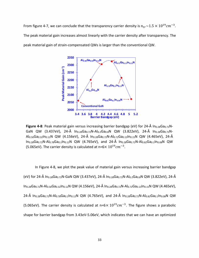
Figure 4-8: Peak material gain versus increasing barrier bandgap (eV) for 24-Å In0.28Ga0.72N-
GaN QW (3.437eV), 24-Å In0.28Ga0.72N-Al0.2Ga0.8N QW (3.822eV), 24-Å In0.28Ga0.72N-
Al0.56Ga0.32In0.12N QW (4.156eV), 24-Å In0.28Ga0.72N-Al0.72Ga0.13In0.15N QW (4.465eV), 24-Å
In0.28Ga0.72N-Al0.78Ga0.1In0.12N QW (4.765eV), and 24-Å In0.28Ga0.72N-Al0.82Ga0.1In0.08N QW
(5.065eV). The carrier density is calculated at n=6× 10¹⁹𝑐𝑚−3.
From figure 4-7, we can conclude that the transparency carrier density is 𝑛𝑡𝑟~1.5 × 10¹⁹𝑐𝑚−3.
The peak material gain increases almost linearly with the carrier density after transparency. The
peak material gain of strain-compensated QWs is larger than the conventional QW.
In Figure 4-8, we plot the peak value of material gain versus increasing barrier bandgap
(eV) for 24-Å In0.28Ga0.72N-GaN QW (3.437eV), 24-Å In0.28Ga0.72N-Al0.2Ga0.8N QW (3.822eV), 24-Å
In0.28Ga0.72N-Al0.56Ga0.32In0.12N QW (4.156eV), 24-Å In0.28Ga0.72N-Al0.72Ga0.13In0.15N QW (4.465eV),
24-Å In0.28Ga0.72N-Al0.78Ga0.1In0.12N QW (4.765eV), and 24-Å In0.28Ga0.72N-Al0.82Ga0.1In0.08N QW
(5.065eV). The carrier density is calculated at n=6× 10¹⁹𝑐𝑚−3 . The figure shows a parabolic
shape for barrier bandgap from 3.43eV-5.06eV, which indicates that we can have an optimized
34
1-nm strain compensated barrier between the bandgap of 4.2eV and 4.4eV for the best gain
properties.
4.3 Summary
In this chapter, we investigate the spontaneous emission characteristics and gain optical
gain characteristics of the conventional and strain-compensated QWs. The spontaneous emission
rate is much larger in low carrier density regime for strain-compensated QWs than the
conventional QW. However, the enhancement factor of the spontaneous emission rate is smaller
in the high carrier density regime than that in the low carrier density regime. The optical gain of
the strain-compensated QWs is larger than that of the conventional QW. The increased electron
and hole wave function overlap due to the better carrier confinement from the AlGaInN barriers
results in an improvement of the spontaneous emission rate. The enhancement of spontaneous
emission and gain properties can be utilized to achieve better optical properties for lasers and
LEDs.
In this chapter, we also draw the conclusion that peak spontaneous emission rate and
peak material gain follow a parabolic shape with an increasing AlGaInN barrier bandgap ranging
from 3.43eV-5.06eV. An optimized 1-nm strain-compensated barrier for 24-Å In0.28Ga0.72N-
AlGaInN QWs can be obtained between the bandgaps of 4.2 eV to 4.4 eV.
35
Chapter 5: Conclusion
In conclusion, this thesis presents a self-consistent simulation study on the spontaneous
emission and optical gain properties of various strain-compensated InGaN–AlGaInN QWs as
active regions for lasers and LEDs with indium content of 28%. In Chapter 1 we presented an
introduction of InGaN-based semiconductors along with current technological challenges and the
concept of strain-compensated quantum wells. We followed this by presenting the self-
consistent 6-band k∙p method in Chapter 2. The Chapter 3 focused on the band properties of
conventional and various strain-compensated quantum well structures. Finally, in Chapter 4 we
investigated the optical properties of the conventional and strain-compensated quantum wells.
From our analysis, both the spontaneous emission spectra and optical gain of strain-
compensated InGaN–AlGaInN QWs reveal significant enhancement in comparison to those of
conventional InGaN–GaN QWs. The strain-compensated InGaN-AlGaInN QWs exhibit 60%-180%
enhancement of the spontaneous emission radiative recombination rate for carrier densities in
the low carrier density regime (from 𝑛 = 1 × 10¹⁸𝑐𝑚−3 up to 𝑛 = 10 × 1018𝑐𝑚−3), which is
serviceable for LED operation. At high carrier densities ( 𝑛 = 2 × 10¹⁹𝑐𝑚−3 up to 𝑛 =
6 × 10¹⁹𝑐𝑚−3), the spontaneous emission radiative recombination rate of strain-compensated
24-Å In0.28Ga0.72N-Al0.2Ga0.8N QW, 24-Å In0.28Ga0.72N-Al0.56Ga0.32In0.12N QW, and 24-Å
In0.28Ga0.72N- Al0.78Ga0.1In0.12N QW are found to be enhanced 22%(12%), 35%(19%), and 32%(16%)
at transparency and threshold conditions, respectively. The strain-compensated 24-Å
In0.28Ga0.72N-Al0.2Ga0.8N QW, 24-Å In0.28Ga0.72N-Al0.56Ga0.32In0.12N QW, and 24-Å In0.28Ga0.72N-
Al0.78Ga0.1In0.12N QW also exhibit improvements of 12.2%, 16.6%, and 14.2%, respectively, for the
36
peak optical gain in comparison to that of conventional InGaN-GaN QW. This finding shows the
potential of a reduction in the threshold carrier density for strain-compensated InGaN-AlGaInN
QW active region. Our study shows a parabolic shape of peak spontaneous emission rate and
peak material gain with increasing barrier bandgap ranges from 3.43eV-5.06eV. This indicates
that one can achieve the best properties for this material system by fabricating an optimized 1-
nm strain compensated barrier for 24-Å In0.28Ga0.72N-AlGaInN QWs between the bandgaps of
4.2eV and 4.4eV. This finding will provide a useful guidance for experimentalist to pursue the
usage of InGaN-AlGaInN QW system as a possible active region for achieving improved
spontaneous emission rate and optical gains for nitride-based photonics devices.
37
References
[1] J.I. Pankove, E.A. Miller, and J.E. Berkeyheiser, "GaN electroluminescent diodes," RCA Rev.,
vol. 32, pp. 383, Oct. 1971.
[2] H.M. Manasevit, "The use of metalorganics in the preparation of semiconductor
materials: growth on insulating substrates," J. of Crys. Gro., vol. 118, pp. 306-314, Apr.
1972.
[3] T. kawabata, T. Matsuda, and S.Koike, "GaN blue light emitting diodes prepared by
metalorganic chemical vapor deposition," J. of Appl. Phys., vol. 56, pp. 2367, May 1984.
[4] H. Amano, M. Kitoh, K. Hiramatsu, and I. Akasaki. Inst Phys Conf Ser No 106: Chapter 10.
[5] S. Nakamura, M. Senoh, and T. Mukai, "High‐power InGaN/GaN double‐heterostructure
violet light emitting diodes", Appl. Phys. Lett., vol. 62, pp. 2390, Feb. 1993.
[6] I. Akasaki, H. Amano, S. Sota, H. Sakai, T.Tanaka, and M. Koike, " Stimulated emission by
current injection from an AlGaN/GaN/GaInN quantum well device", Jpn. J. Appl. Phys.,
vol. 34, pp. 1517, Aug. 1995.
[7] "The Nobel Prize in Physics 2014". [Online]. Available:
https://www.nobelprize.org/nobel_prizes/physics/laureates/2014/. [Accessed: 10-Dec-
2017].
[8] H.P.Zhao, R.A. Arif, Y.Khoon Ee, and N.Tansu, "Self-consistent analysis of strain-
compensated InGaN-AlGaN quantum wells for lasers and light-emitting diodes,"IEEE
38
J.Quantum Electron., vol.45, no.1, pp.66-78, Jan. 2009.
[9] N. Tansu, N. J. Kirsch, and L. J. Mawst, “Low-threshold-current-density 1300-nm dilute-
nitride quantum well lasers,” Appl. Phys. Lett., vol. 81, pp. 2523–2525, Sep. 2002.
[10] N. Tansu, J. Y. Yeh, and L. J. Mawst, “Extremely low threshold-current-density InGaAs
quantum well lasers with emission wavelength of 1215–1233 nm,” Appl. Phys. Lett., vol.
82, pp. 4038–4040, Jun. 2003.
[11] N. Tansu, J. Y. Yeh, and L. J. Mawst, “Physics and characteristics of 1200-nm InGaAs and
1300–1400 nm InGaAsN quantum-well lasers by metalorganic chemical vapor
deposition,” IOP J. Physics: Condens. Matter Phys., vol. 16, pp. S3277–S3318, Aug. 2004.
[12] S. J. Chang, C. H. Kuo, Y. K. Su, L. W. Wu, J. K. Sheu, T. C. Wen, W. C. Lai, J. F. Chen, and J.
M. Tsai, “400-nm InGaN-GaN and InGaN-AlGaN multiquantum well light-emitting diodes,”
IEEE J. Sel. Topics Quantum Electron., vol. 8, no. 4, pp. 744–748, Aug. 2002.
[13] N. Tansu, J. Y. Yeh, and L. J. Mawst, “Experimental evidence of carrier leakage in InGaAsN
quantum well lasers,” Appl. Phys. Lett., vol. 83, pp. 2112–2114, Sep. 2003.
[14] N. Tansu and L. J. Mawst, “Current injection efficiency of 1300-nm InGaAsN quantum-
well lasers,” J. Appl. Phys., vol. 97, pp. 2523–2525, Mar. 2005.
[15] T. Fukunaga, M. Wada, and T. Hayakawa, “Reliable operation of strain-compensated
1.06 m InGaAs/InGaAsP/GaAs single quantum well lasers,” Appl. Phys. Lett., vol. 69, pp.
248–250, Jul. 1996.
[16] S. L. Chuang and C. S. Chang, “k∙p method for strained wurtzite semiconductors,” Phys.
39
Rev. B., vol. 54, pp. 2491–2504, Jul. 1996
[17] S. L. Chuang, “Optical gain of strained wurtzite GaN quantum-well lasers,” IEEE J.
Quantum Electron., vol. 32, no. 10, pp. 1791–1800, Oct. 1996.
[18] C. Kittel, "Quantum Theory of Solids (Second Revised Printing ed.)", New York: Wiley.
pp. 186–190. ISBN 0-471-62412-8
[19] F. Bernardini and V. Fiorentini, “Spontaneous versus piezoelectric polarization in III–V
Nitrides: Conceptual aspects and practical consequences,” Phys. Stat. Sol. (b), vol. 216,
pp. 391–398, Nov. 1999.
[20] O. Ambacher, J. Majewski, C. Miskys, A. Link, M. Hermann, M. Eick-hoff, M. Stutzmann, F.
Bernardini, V. Fiorentini, V. Tilak, W. J. Schaff, and L. F. Eastman, “Pyroelectric properties
of Al(In)GaN/GaN hetero and quantum well structures,” J. Phys.: Condens. Matter, vol.
14, pp. 3399–3434, Mar. 2002.
[21] I. Vurgaftman and J. R. Meyer, “Band parameters for nitrogen-containing
semiconductors,” J. Appl. Phys., vol. 94, pp. 3675–3696, Sep. 2003.
[22] S. L. Chuang, Physics of Optoelectronics Devices. New York: Wiley, 1995, ch. 4 and 9
[23] S. L. Chuang and C. S. Chang, “A band-structure model of strained quantum-well wurtzite
semiconductors,” Semicond. Sci. Technol., vol. 12, pp. 252–263, 1997
[24] M.Rowe, P.Michler, J.Gutowski, V. Kummler, A.Lell, and V.Harle, "Influence of the carrier
density on the optical gain and refractive index change in InGaN laser strucuture,"
Phys.Stat.Solid(A), vol.200, pp. 135-138, Sep.2003
40
Vita
Hanlin Fu was born on February 3, 1993, in Dalian, China to Shouchen Fu and Yuehua Pei.
He entered the University of Science and Technology of China in 2011 and graduated with a
Bachelor’s of Science in Atomic and Molecular Physics. He did research projects in Chinese
Academy of Science as a research assistant from September 2015 to June 2016. He started his
graduate studies in Electrical Engineering at Lehigh University under his adviser Professor Nelson
Tansu in 2016. With this thesis, he will graduate with a Master’s of Science in Electrical
Engineering in December 2017.