WOCSDICE : workshop on compound semiconductor devices ...
144
WOCSDICE : workshop on compound semiconductor devices and integrated circuits, 21st, May 25-28, 1997, Scheveningen, The Netherlands Citation for published version (APA): Roer, van de, T. G. (1997). WOCSDICE : workshop on compound semiconductor devices and integrated circuits, 21st, May 25-28, 1997, Scheveningen, The Netherlands. (WOCSDICE : workshop on compound semiconductor devices and integrated circuits; Vol. 21). Technische Universiteit Eindhoven. Document status and date: Published: 01/01/1997 Document Version: Publisher’s PDF, also known as Version of Record (includes final page, issue and volume numbers) Please check the document version of this publication: • A submitted manuscript is the version of the article upon submission and before peer-review. There can be important differences between the submitted version and the official published version of record. People interested in the research are advised to contact the author for the final version of the publication, or visit the DOI to the publisher's website. • The final author version and the galley proof are versions of the publication after peer review. • The final published version features the final layout of the paper including the volume, issue and page numbers. Link to publication General rights Copyright and moral rights for the publications made accessible in the public portal are retained by the authors and/or other copyright owners and it is a condition of accessing publications that users recognise and abide by the legal requirements associated with these rights. • Users may download and print one copy of any publication from the public portal for the purpose of private study or research. • You may not further distribute the material or use it for any profit-making activity or commercial gain • You may freely distribute the URL identifying the publication in the public portal. If the publication is distributed under the terms of Article 25fa of the Dutch Copyright Act, indicated by the “Taverne” license above, please follow below link for the End User Agreement: www.tue.nl/taverne Take down policy If you believe that this document breaches copyright please contact us at: [email protected] providing details and we will investigate your claim. Download date: 04. Feb. 2022
-
Upload
khangminh22 -
Category
Documents
-
view
1 -
download
0
Transcript of WOCSDICE : workshop on compound semiconductor devices ...

WOCSDICE : workshop on compound semiconductor devicesand integrated circuits, 21st, May 25-28, 1997, Scheveningen,The NetherlandsCitation for published version (APA):Roer, van de, T. G. (1997). WOCSDICE : workshop on compound semiconductor devices and integratedcircuits, 21st, May 25-28, 1997, Scheveningen, The Netherlands. (WOCSDICE : workshop on compoundsemiconductor devices and integrated circuits; Vol. 21). Technische Universiteit Eindhoven.
Document status and date:Published: 01/01/1997
Document Version:Publisher’s PDF, also known as Version of Record (includes final page, issue and volume numbers)
Please check the document version of this publication:
• A submitted manuscript is the version of the article upon submission and before peer-review. There can beimportant differences between the submitted version and the official published version of record. Peopleinterested in the research are advised to contact the author for the final version of the publication, or visit theDOI to the publisher's website.• The final author version and the galley proof are versions of the publication after peer review.• The final published version features the final layout of the paper including the volume, issue and pagenumbers.Link to publication
General rightsCopyright and moral rights for the publications made accessible in the public portal are retained by the authors and/or other copyright ownersand it is a condition of accessing publications that users recognise and abide by the legal requirements associated with these rights.
• Users may download and print one copy of any publication from the public portal for the purpose of private study or research. • You may not further distribute the material or use it for any profit-making activity or commercial gain • You may freely distribute the URL identifying the publication in the public portal.
If the publication is distributed under the terms of Article 25fa of the Dutch Copyright Act, indicated by the “Taverne” license above, pleasefollow below link for the End User Agreement:www.tue.nl/taverne
Take down policyIf you believe that this document breaches copyright please contact us at:[email protected] details and we will investigate your claim.
Download date: 04. Feb. 2022

**** WOCSDICE 97 ****
21st Workshop on Conlpound SemiconductorDevices and Integrated Circuits
May 25-28, 1997Scheveningen, The Netherlands
Edited by:Th.G. van de Roer
Eindhoven University of TechnologyP.O. Box 513 - ER8
NL-5600 ME Eindhoven, The NetherlandsTel. +31.40.247.5106Fax +31.40.244.8375
E-mail [email protected]

CIP-DATA LIBRARY EINDHOVEN UNIVERSITY OF TECHNOLOGY
van de Roer, Th.G.
WOCSDICE9721 st Workshop on Compound Semiconductor Devices and Integrated Circuits
Eindhoven: Eindhoven University of Technology, 1997.
ISBN 90-9010767-3NUGI832
Trefwoorden : halfgeleidercomponenten, micr()golfhalfgeleiders,galliumarsenidetransistoren, halfgeleiderlasers.Subject Headings: compound semiconductors, microwave transistors,integrated circuits, semiconductor lasers, integrated optics.

Advisory Committee:
Werner Baechtold, Swiss Federal Institute of Technology (Switzerland)Lester Eastman, Cornell University (USA)Fausto Fantini, Parma University (Italy)Hans Hartnagel, Darmstadt Technical University (Gennany)William Kelly, NMRC (Ireland)Erhard Kohn, Ulm University (Gennany)Didier Lippens, illS (France)Arvydas Matulionis, Semiconductor Physics Institute (Lithuania)Elias Munoz Merino (Spain)Vernon Morgan, Cardiff University (UK)Dimitris Pavlidis, University ofMichigan (USA)Peter Robson, Sheffield University (UK)Jan Soederstroem, Ericsson (Sweden)Hartwig Thim, Linz University (Austria)
Workshop Organisers:Theo van de Roer, Leon Kaufinann,Eindhoven University and COBRA Research Institute,Eindhoven, The Netherlands
Workshop Secretaries:Mrs Tine Bijl, Mrs. Els Gerritsen
Fax: +31.40.244.8375Phone: +31.40.247.5106(5133,5134)e-mail: [email protected]@ele.tue.nl
2

Invited Speakers:
Prof Lester F. EastmanCornell University, Phillips HallIthaca NY 14853, U.S.A.
Dr. Takatomo EnokiHeterostructure Devices Research GroupAdvanced Devices and Technology LaboratoryNTT Systems Electronics Laboratories3-1 Morinosato-WakamiyaAtsugi, Kanagawa Pref., 243-01 Japan
ProfDr. K. EnsslinLaboratorium fuer FestkoerperphysikETR HoenggerbergCH-8093 Zurich, Switzerland
Prof. Fausto FantiniUniversita degli Studie di ParmaDipartimento di Ingegneria dell'lnformazioneViale delle Scienze1-43100 Parma, Italy
Dr. G. GattiESTECP.O. Box 299NL-2200 AG Noordwijk, The Netherlands
Prof. Dr. K. Von KlitzingMax Planck Institut fuer FestkoerperphysikHeisenbergstrasse 1D-70569 Stuttgart, Germany
Dr. Meint K. SmitTechnische Universiteit DelftFaculteit ElektrotechniekMekelweg42628 CD Delft, The Netherlands
Dr. Dwight StreitTRW Electronic Systems GroupOne Space ParkRedondo Beach CA 90278, U.S.A.
Dr. Masafumi YamamotoQuantum Effect Devices Research GroupAdvanced Devices and Technology LaboratoryNTT Systems Electronics Laboratories3-1 Morinosato-WakamiyaAtsugi, Kanagawa Pre£., 243-01 Japan
3

WOCSDICE 97 is sponsored by:
COBRA Research InstituteEindhoven university of TechnologyP.O. Box 513NL-5600 MB EindhovenThe Netherlands
European Office ofAerospace Research and Development,European Research Office,Office ofNaval Research,223 Old Marylebone RoadLondon NWI 5TH, England
AixtronSemiconductor Technologies GmbHKackertstrasse 15 - 170-52072 AachenGermany
JEOLTupolevlaan 28a1119 NZ Schiphol - RijkThe Netherlands
Oxford Instruments GmbHSemiconductor Systems DivisionPlasma TechnologyP.O. Box 4509D-55035 WiesbadenGermany
TNO-FELOude Waalsdorperweg 63Postbus 96864NL-2509 JG Den HaagThe Netherlands
A. De Jong B.V.Postbus 11001NL-3004 EA RotterdamThe Netherlands
III-V's Review
SENTERlOP Electro-OpticsGrote Marktstraat 43Postbus 30732NL-2500 GS Den HaagThe Netherlands
4

Sunday, May 25
19.00 Welcome Reception
WOCSDICE97
Programme
5

Monday, May 26, morning
8.30 • 8.40 Opening and Welcome
8.40 • 10.10 Session 1: Reliability and Characterization
08.40 1. (Invited Paper) F. Fantini, Parma University:"Reliability and degradation of HEMTs and HBTs"
09.10 2. K. Lipka, P. Schmid, J. Ibbetson, N. Nguyen, U. Mishra and E. Kohn:"High Temperature Operation of GaAs Based HFET Structure ContainingLayers Grown at Low Temperature ".
3. J. Grajal de la Fuente, V. Krozer, M Schu13ler, M. Brandt, H. Hartnagel:"Application of Semiconductor Interface Modelling to ReliablityCharacterisation".
4. G. Meneghesso, G. Peloso, A. Neviani, M Hurt, X. Peatman, M Shur, E.Zanoni:"Study of breakdown mechanism in 2D MESFETs".
5. D. V. Morgan, Y.H. Aliyu and H. Thomas:"Metal probe technique for characterisation of semiconductor materialsused in optoelectronic devices".
6. S. Mohammadi, D. Pavlidis, B. Bayraktaroglu:"A Novel Approach for Determining the Reliability of AIGaAs/GaAs HBTsfrom Low-Frequency Noise Characteristics"
10.10 • 10.40 Coffee Break
10.40 • 12.35 Session 2: Optoelectronics
10.40 1. (Invited Paper) MK. Smit, Y.-S. Dei, Delft University, T. Staring, PhilipsOptoelectronics:
"Photonic Integrated Circuits for multiwavelength applications"
11.10 2. B.H.P. Dorren, A. Yu. Silov, M.R Leys, J.EM Haverkort, J.H. Wolter,D.H.P. Maat, Y. Zhu, Y.S. Dei, F.H. Groen:
"Polarization independent InGaAs/lnP chopped quantum wellinterferometric space switch at 1.55 IJm".
3. C. Llorente, R.M. Lorenzo, A. Sanz, I. De Miguel, EJ. Abril, M L6pez, M Aguilar:"Design and analysis of a 1 x 8 wavelength division multiplexer based on
the self-imaging theory".4. RM. Lorenzo, C. Llorente, I. De Miguel, EJ. Abril and M. L6pez:
"Design and analysis of a 1 x 32 tapered coupler based on the selfimaging theory".
5. R Hakimi, B. Schmidt and M-C. Amman:"Reduced Spectral Linewidth of Tunable Twin Guide Laser Diodes withBuried Facet Structure".
6. W Steffens and M-C. Amman:"Effect of internal reflections on wavelength selectivity in widely tunablelaser diodes".
7. D.A. Tkachenko, D.G. Baksheyev and V.A. Tkachenko:"Irradiated quantum well in a potential step as photon source and electronpump".
8. B. Willen, U Westergren:"HBT-based PIN diodes for high-speed OEIC-receivers".
12.35 Lunch
6

Monday, May 26, afternoon
14.00 - 15.30 Session 3: Integrated Circuits and Noise
14.00 1. (Invited Paper) G. Gatti, ESTEC:"Space applications of GaAs MMICs"
14.30 2. J. Bemtgen, M Heuken and K. Heime:"The influence of the cap layer on the low frequency noise of 2DEGstructures".
3. A Matulionis, J. Liberis, I. Matulioniene, P. Gottwald, J. Karanyi, B. Szentpali,HL. Hartnagel, K. Mutamba, A Sigurdad6ttir:
"Hot-Electron Diffusion Coefficient in Standard Doped InP Channels".4. AP. de Hek, F.L.M. van den Bogaart:
"Broadband High Efficient X-band MMIC Power Amplifiers for FutureRadar Systems".
5. F.E. van Vliet, J.L. Tauritz, F.L.M. van den Bogaart:"On the Design and Application of Narrow tunable MMIC Filters".
6. P. Marsh, D. Pavlidis:"Noise Analysis of InGaAs Mixer Diodes at Millimeter Wave and Far-InfraredFrequencies"
15.30 - 16.10 Coffee Break
16.10 - 18.00 Session 4: Quantum Effects and Tunneling
16.10 1. (Invited Paper) K. Von Klitzing, Max Planck Institute Stuttgart:"Semiconductor quantum devices"
16.40 2. (Invited Paper) M Yamamoto, NIT System Electronics Labs.:" Resonant Tunneling Diode and HEMT Integrated Devices and Circuits".
17.10 3. A Sigurdardottir, K. Mutamba, A Vogt and H L. Hartnagel:"Investigation on Tunnelling Effect in Stressed InAs/AISb/GaSb-ResonantTunnelling Diodes".
4. MI. Lepsa, Th.G. Van de Roer, J.J.M. Kwaspen, W Van der Vleuten,L.M.F. Kaufmann:
"Three Terminal Double Barrier Resonant Tunneling Devices Based onthe Direct Contacting of the Quantum Well".
5. Jozsef Karanyi and Bela Szentpali:"Quantum mechanical tunneling in GaAs ohmic contacts".
6. J.J. M. Kwaspen, MI. Lepsa, Th.G. Van de Roer, W Van der Vleuten,HC. Heyker, L.M.F. Kaufmann:
"Accurate Equivalent-Network Modeling of GaAs/AIAs Based ResonantTunneling Diodes with Symmetrical Thin Barrier and Spacer Layers"
19.00 Dinner
7

Tuesday, May 27
8.30 - 10.00 Session 5: Novel Techniques and Devices
08.30 1. (Invited Paper) K. EnssJin, Swiss Federallnstitue of Technology:"Ballistic electron transport in semiconductor nanostructures"
09.00 2. Nils G. Weimann and Lester F, Eastman:"Effect of Threading Dislocations on the Electron Mobility in GaN andits consequences for Vertical Devices",
3. P. Gluche, A. Aleksov, A. Vescan, W Ebert and E. Kohn:"A Technical Approach Towards Diamond Power Transistors".
4. G. Hock, A. Gruhle, T. Hackbarth, E Kohn and U. Konig:"High Current Sio.3Geo.7 p-Channel Hetero MOSFETs",
5. D.A. Romanov, EB. Gorokhov, V.A. Tkachenko and O.A. Tkachenko:"Insertion of slipping planes in quantum well with 2DEG for creating onedimensional -barriers",
6. F. Ejeckam, Yu-Hwa Lo, M. Seaford, L.F. Eastman:"Lattice Constant Engineering Using Compliant Universal (C.U.) Substrates".
10.00 - 10.30 Coffee Break
10.30 - 12.30 Session 6: Field Effect Transistors and Diodes
10.30 1. (Invited Paper) T. Enoki, NIT System Electronics Labs.:"lnP-basedHEMT ICs for ultra high speed optical communication systems"
11.00 2. He/mut Brech, Thomas Simlinger, Thomas Grave and Siegfried Seiberherr:"Influence of Gatelength on the DC-Characteristics and fr ofPseudomorphic Power-HEMTs".
3. R. Fauquembergue, P. Desplanques, F. Dessenne and D. Cichoka:"Monte Carlo Simulation of III-V Nitrides FET's",
4. F. Fumi, M. Peroni, C. Lanzieri, A. Cetronia, A. Gasparotto:"Optimalization of multifunction self-aligned-gate (MSAG) GaAs MESFET".
5. D. Theron, S. Piotrowicz, X. Wal/art, F. Diette, B. .Bonte and Y, Crosnier:"lnP based HEMT structures with a large bandgap barrier layer for powerapplication in V band".
6. Ferdouse Khaleque:"Room temperature InSb MISFETs".
7. K. LObke, T. Hi/garth, Ch. Diskus, A. Stelzer, A. Springer and H. W Thim:"Zero-bias Detection with InO.38GaO.62As Schottky Barrier Diodes".
8. X. Melique, E Lheurette, P. Mounaix, F. Mol/ot, O. Vanbesien and D. Lippens:"lnP-based Heterostructure Barrier Varactor".
12.30 Lunch
14.00 - ca. 23.00 Excursion and Banquet
8
Wednesday, May 28
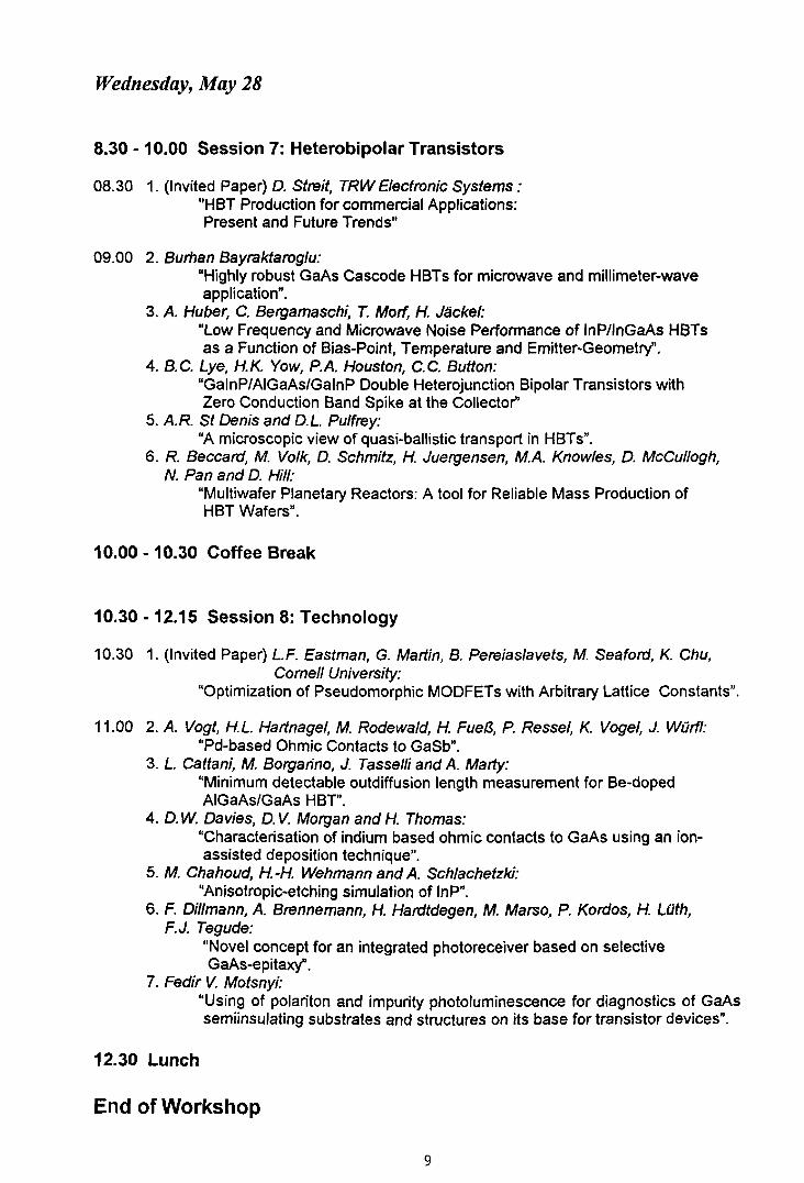
8.30 - 10.00 Session 7: Heterobipolar Transistors
08.30 1. (Invited Paper) D. Streit, TRW Electronic Systems:"HBT Production for commercial Applications:Present and Future Trends"
09.00 2. Burhan Bayraktaroglu:"Highly robust GaAs Cascode HBTs for microwave and millimeter-waveapplication".
3. A. Huber, C. Bergamaschi, T. Mort, H. Jackel:"Low Frequency and Microwave Noise Performance of InPllnGaAs HBTsas a Function of Bias-Point, Temperature and Emitter-Geometry".
4. B.e. Lye, H.K. Yow, P.A Houston, e.C. Button:"GalnP/AIGaAs/GalnP Double Heterojunction Bipolar Transistors withZero Conduction Band Spike at the Collector"
5. AR. St Denis and D.L. Pulfrey:"A microscopic view of quasi-ballistic transport in HBTs".
6. R. Beccard, M. Volk, D. Schmitz, H Juergensen, MA Knowles, D. McCullogh,N. Pan and D. Hill:
"Multiwafer Planetary Reactors: A tool for Reliable Mass Production ofHBT Wafers".
10.00 - 10.30 Coffee Break
10.30 -12.15 Session 8: Technology
10.30 1. (Invited Paper) L.F. Eastman, G. Martin, B. Pereias/avets, M Seaford, K. Chu,Cornell University:
"Optimization of Pseudomorphic MODFETs with Arbitrary Lattice Constants".
11.00 2. A. Vogt, HL. Hartnage/, M Rodewald, H FuefJ, P. Ressel, K. Vogel, J. Wilrtl:"Pd-based Ohmic Contacts to GaSb".
3. L. Cattani, M Borgarino, J. Tasselli and A Marty:"Minimum detectable outdiffusion length measurement for Be-dopedAIGaAs/GaAs HBT".
4. D. W. Davies, D. V. Morgan and H. Thomas:"Characterisation of indium based ohmic contacts to GaAs using an ionassisted deposition technique".
5. M. Chahoud, H.-H Wehmann and A. Schlachetzki:"Anisotropic-etching simulation of InP".
6. F. Oil/mann, A Brennemann, H. Hardtdegen, M Marso, P. Kordos, H Lilth,F.J. Tegude:
"Novel concept for an integrated photoreceiver based on selectiveGaAs-epitaxy".
7. Fedir V. Motsnyi:"Using of polariton and impurity photoluminescence for diagnostics of GaAssemiinsulating substrates and structures on its base for transistor devices".
12.30 Lunch
End of Workshop
9

Monday, May 26
8.40 - 10.15 Session 1: Reliability and Characterization
08.40 1. (Invited Paper) F. Fantini, Parma University:"Reliability of heterostructure devices"
09.10 2. K. Lipka, P. Schmid, J. Ibbetson, N. Nguyen, U. Mishra and E. Kohn:"High Temperature Operation of GaAs Based HFET StructureContaining Layers Grown at Low Temperature".
3. Jesus Grajal de la Fuente, Viktor Korzer, Martin SchOl3ler, MichaelBrandt and Hans Hartnagel:
"Application of Semiconductor Interface Modelling to ReliablityCharacterisation".
4. G. Meneghesso, G. Peloso, A. Neviani, M. Hurt, X. Peatman, M. Shur,E. Zanoni:
"Study of breakdown mechanism in 20 MESFETs".
5. D. V. Morgan, Y.H. Aliyu and H. Thomas:"Metal probe technique for characterisation of semiconductormaterials used in optoelectronic devices".
6. S. Mohammadi, D. Pavlidis, B. Bayraktaroglu:"A Novel Approach for Determining the Reliability of AIGaAs/GaAsHBTs from Low-Frequency Noise Characteristics"
10

Reliability and degradation of HEMTs and HBTs
Fausto Fantini, Paolo Cova, Mattia Borgarino, Laura Cattani, and Roberto Menozzi
University of Parma, Dipartimento di Ingegneria dell'InformazioneViale delle Scienze, 43100 Parma, Italy
The reliability of heterojunction devices, in particular HEMTs and HBTs, is quite a new item, sothat research efforts are still mainly concentrated onthe end-life problems. Electronic devices manufactured with compound semiconductors are quite different and numerous, so that the failure mechanismstoo are various; nevertheless it is possible to identify some points in common with MESFETs [1], themost mature and widespread product in the compound semiconductors technology:
1. the absence of a natural surface passivation;2. the impossibility to make a mono-metal sys
tem;3. the low resistance to EOS/ESD.
On the other hand, since in HBTs the heterojunction may conduct high currents, they also exhibitdegradation mechanisms similar to those of opticaldevices, in particular related to the growth of crystaldefects.
In this paper we report on the reliability ofHEMTs and HBTs, mainly looking at the end-lifeproblems and related physical mechanisms. Notenough data have been collected up to now to givereliable figures on the failure rates. Nearly all thecomponents here taken into account are based onGaAs substrates: only few results on InP based devices are available untill now.
HEMTDuring the last ten years the HEMT has substituted the MESFET in many applications, becausehis higher speed, but the understanding of the failure mechanisms induced by stress tests and their relationship with failures occurring in operating conditions is still far from being complete and satisfactory.It is possible to group the observed failure mechanisms in four categories.
EOS, ESD, and burn-out. It is usually verydifficult to analyse compound semiconductor devicesfailed in field for EOS (Electrical Over-Stress) andESD (Electro-Static Discharge) because, due to theirintrinsic weakness (very short and large channels,very short gate-drain and gate-source distances), theyappear often completely destructed [2, 3]. The modeof failure is termed "burn-out", whereas the causemay be an EOS or an ESD, for whitch HEMTshave a very low threshold value (according with theHuman Body Model), in the order of a few hundred volts, so that the handling precautions becomemandatory for these devices. The high energy involved in the ESD phenomenon frequently induces
11
major damage in the devices, similar to that causedby surcharge effects, due to pulses that are quitecommon in the RF applications. However, burn-outcan also occur in the absence of any overstress effect.The cause of the failure is usually a short-circuit between the electrodes under bias. The origin of theshort is located either on the surface between thegate and drain, or at the interface between the channel and the buffer layer [4]. The mechanism can beeither the semiconductor oxidation, with the consequent formation of GaO and then a metallic path,due to the excess As, or Au electromigration fromthe drain towards the gate, along the surface. Inexperiments made on AIGaAs/GaAs HEMTs [5] adegradation of the Schottky barrier after ESD stresswas found.
Ohmic contacts. The Au-Ge-Ni multilayer ismost frequently used. The failure mechanism is theincrease of the resistance at high temperatures (>200 0c), probably due to the Ga out-diffusion. Theactivation energy is very high, so that it is not easy toextrapolate these data to the operating conditions.This problem was experienced also in the ohmic contacts for power devices, but it is possible to overcame this limit by using large Au stripes, which areless sensitive to this phenomenon. It was recentlyclaimed [6] the dependence of the degradation on thestress type: failure mechanisms in the case of hightemperature storage, DC bias and DC bias with RFsuperimposed differ signiftcantly and the contactsdegrade more rapidly under RF life testing. Unfortunately no clear physical explanation of this behaviorwas proposed up to now. It was found a decrease intransconductance related to ohmic contact damage.RF life tests have also shown [7] a decrease of draincurrent, transconductance and gain and an increasein noise figure, attributed to gate metal (Ti/Pt/Au)interdiffusion and ohmic contact (Au-Ge-Ni) degradation. In [8] HEMTs were submitted to HTS andoperating life tests and the degradation was associated with significant amount of Ga and As outdiffusion through the ohmic areas. A TiN barrierplaced between the AuGe/Ni/Au contact and theTi/Pt/Au overlay metal was found to be effectivein eliminating this degradation and increasing themean time to failure.
Schottky contacts. Even the gate contact degradation is less important than for MESFETs, dueto the distance from the channel, the barrier heightdetermines device characteristics. Various effects,depending on the barrier material, were found.

In [9] HEMTs with Al/Ti and Al/Ni Schottkycontacts were compared by means of bias and thermal stress. For AI/Ti contacts, a decrease in barrierheight was observed under storage tests up to 2750G'. The formation of metallic compounds, such asAbTi, is believed to be responsible for this decrease.On the contrary, AI/Ni Schottky contacts showed anincrease of the barrier height: either the migrationof Ni into the Al film or the reaction of Ni with GaAsare possible explanations in this case [10]. As shownin the Arrhenius plot of Fig. 1, an activation energyEa =1.7 eV was obtained.
At higher temperature (300°C) the reaction between Al and Au leads to the catastrophic failurewell known as "purple plague" .
Hot carriers. Interface states at the GaAs surface in the area between gate and drain and electrontraps related to DX centers in the doped AIGaAslayer were indicated as the cause of parasitic effects,such as the presence of kink in the output characteristics. Moreover, these centers are responsible for thedegradation of the transconductance for positive values of the gate voltage and they can affect the devicelife. The sensit.ivity of the HEMT drain characteristics to hot electrons and thermal stress cycles, dueto the enhancement and depletion of these centerswas observed [II]. It has also been observed a correlation between the "kink" effect and the variation ofthe frequency dispersion of the output conductance,attributed to that deep levels present in the AIGaAslayer.
Unpassivated AIGaAs/GaAs HEMTs showed rapid and irreversible degradation of the electrical characteristics, induced by hot electrons: decrease indrain current and increase in transconductance frequency dispersion [12].
In [13], it was reported that the gate breakdownvoltage of an unpassivated AIGaAs/GaAs HEMTcan move to higher negative values when a current isallowed to flow through the gate under reverse gatebias voltage. When a reverse bias is applied betweenthe gate and source, this breakdown "walkout" canbe accompanied by a permanent increase in devicesource resistance and decreases in gm and IDss. Asimilar effect was observed in AIGaAs/InGaAs/GaAsPHEMTs and in GaAs MESFETs, but not in SiNpassivated devices, so that an explanation could bethe oxidation of the exposed AIGaAs/GaAs layersnear to the recessed gate edges, where the electricfield is the highest. The oxidation may result fromthe humidity present in the air and the avalanchingprocess under a high reverse gate bias.
Studies on dual channel HEMTs ICs were performed [14], and the importancf' of the electron channels separation distance on the reliability of these devices was underlined. The failure mechanisms weretrap generation at the donor layer-GaAs interface,increased impurity concentration in the GaAs separating the two channels and metal migration (Au),primarily from the ohmic contacts.
12
PHEMTsAn additional source of degradation for AIGaAs/InGaAs/GaAs PHEMTs could be the generation oftraps in the InGaAs strained layer, due to the growthof edge dislocations in the [100] directions [IS].
Lifetesting experiments [16] have been carriedout in order to assess the stability of the InGaAsburied strained layer and related interfaces duringoperation, indicating that interfaces of InGaAsstrained quantum well HEMTs do not induce particular degradations after 3000 hours into biased agingtests, although deep level centers appear in the nAIGaAs layer.
Although aluminium molar fraction of PHEMTis lower than for lattice matched AIGaAs/GaAsHEMT, instabilities of the electrical characteristicsinduced by DX-centers, accelerated by the temperature, were recently found [17].
About the sensitivity of PHEMTs to hot electrons, tests on commercial devices [18] showed different behaviors. In some case it was found a recoverable (the devices recovered theirs original characteristics after some tenth of hours) increase of the draincurrent and consistent negative shift of the threshold voltage (Fig. 2), probably due to enhancementdepletion of traps below the gate; storage tests (without bias) at 180°C gave rise to the same results. Thistype of degradation has been recently demonstrated[I9j to be in a strict correlation with the change ofthe RF direct gain S21 (Fig. 3). In other devices[20] a permanent gate-drain breakdown walkout appeared (Fig. 4); the explanation is that, possiblydue to negative fixed charge generation in the gatedrain region, where the electric field is very high andimpact ionization takes place, anew) more relaxeddistribution of the field arises, increasing the voltageneeded for t.he breakdown, so that it is possible torise the level of the hot electrons stress (higher VDS)
and furthermore to increase the breakdown voltage.
HBTsHeterojunction bipolar transistors have received considerable attention as devices for high speed andhigh frequency applications owing a number of advantages over other devices. A cutoff frequency Itof S9 GHz and a maximum oscillation frequency1max of 68 GHz have already been demonstrated inGaInP/GaAs system [21]. In spite of these very attractive performances, a lot of efforts are required inorder to improve the device stability and reliability.
A primary reliability issue is the investigation ofthe base dopants stability, particularlY Be and C.The most serious concern in using Be is the dopingimpurities diffusion from the base into the emitterlayer during the transistor operation. The experimental data on the activation energy concerning thecurrent peak degradation of tunnel diodes [22] andthe numerical investigations concerning the DHBTdegradation [23] suggest a recombination-enhanceddiffusion of Be interstitials. The diffusion affects

the threshold voltage VBEth, which is a parameterwidely employed to monitor the device degradationduring an accelerated lifetesting. An increase in thethreshold voltage is usually reported as consequenceof the Be diffusion towards the emitter layer [24-31]
A number of other related phenomena are reported such as an increase of the offset voltage [28],of the collector current ideality factor [28] and of theinverted collector current ratio [32]. Concerning themicrowave characteristics, a decrease of the cutofffrequency It and an increase of the maximum oscillation frequency Imax were observed [28].Several solutions have been proposed to improve thedevice stability.An undoped setback layer placed between base andemitter is employed in order to reduce the impact ofthe diffusion on the electrical characteristics of thedevice. This is the case, even if a small negative shiftof the threshold voltage can be observed, as shownin Fig. 5 [23].
Also a graded emitter layer reduces the sensitivity of the HBTs to the base dopant out-diffusion.Since the diffusion coefficient is inversely proportional to the gallium vacancies concentration [33] theBe stability can be improved by growning epitaxiallythe wafer with a high V/III beam flux ratio [34].
The dependence of the diffusion on the mechanical stress [25, 35] can be employed to improve the Bestability, as demonstrated in [36] and more recentlyin [37], because the finite mechanical strain, inducedby a superlattice structure at the emitter-base junction, inhibits the diffusion of interstitial atoms.
In a recent work [38] it was suggested that aBe concentration of 1019cm-3 should be consideredan upper limit to the base dopant level concentration for the fabrication of a reliable device. In lightof these considerations other materials were usedas an alternative p-type dopant to Be, such as Cand Zn [39]. The behavior of C-, Zn-, and Bedoped base HBTs (C=5xl019 cm-3 , Zn=4xl018
cm-3 , Be=4x 1018 cm-3 ) was compared under identical bias stress conditions. For both Zn- and Bedoped devices a significant shift in VBEth was observed together with a decrease in gain. No significant change was detected for C-doped base devices. Therefore an attractive choice for HBTs using a very high base dopant concentration is carbon,thanks of his very low diffusion coefficient [26, 40].This is likely a consequence of the fact that C occupies the As rather than the Ga sublattice, as in caseof the Be impurities [41]. In spite of his low diffusivity, the C atoms suffer from a stability problemdue to his inclination to the formation of C-H complexes [42] in presence of hydrogen contamination.SIMS analysis demonstrated that hydrogen is incorporated during MOCVD growth [43-46] and alsothat it can be absorbed during a plasma depositionofSiNr [47] or introduced by a H+ implant isolation[48]. The effect of a carbon passivation by H atomsis a time-dependent current gain, a behavior which
13
negatively affects the device reliability. A decreaseof the current gain was ascribed to the debonding ofH from the C acceptors, probably enhanced by minority carrier injection [42]. This mechanism shouldgive rise to an increase of the effective base doping [43, 45]. During current stress tests of C-dopedHBTs an initial current gain increase has also beenobserved [43, 49, 50], as reported in Fig. 6. Thisbehavior has been explained by the reduction of recombination centers involving hydrogen atoms [49]and it seems to affect also the low frequency noisespectra of the HBT [50].
The use of carbon as base dopant may originatenot only hydrogen related instability. Due to thesmall covalent bonding radius of C [51], a high carbon concentration is responsible for a lattice contraction. The associated lattice mismatch inducesa mechanical stress, that can affect the HBT reliabilit.y, as already observed in the case of the laser[52]. This agrees with the reliability similarities between HBT and laser proposed in [38]. The codopingwith indium of heavily C-doped base layer releasesthe strain induced by the C impurities and thereforeimproves the HBT stability [53].
About ohmic contacts in HBTs, the main issueis the increase in the contact resistance during device operation. A number of metal systems has beenproposed for both p-type and n-type ohmic contactseither alloyed or non alloyed and investigated undert.hermal st.ress.
AuGe/Ni/Ti/Au alloyed contacts to n-type GaAs,degrade under thermal stress. Ga and Au interdiffusion is believed to be responsible for this degradation[:31]. In AuGe/Ni/Ti/Pt/Au contacts, the insertionof Pt contributes to block Au diffusion. Thicknesslower than 50 nm leads to an improvement of thecontact stability [54].
Systems using refractory materials were also investigated for p-type contacts, such as Pt/W/ Ag,Pt/Zn/Au and Pt/Ti/Pt/Au. Not only do thesecontacts provide low resistivity, but they are alsoreliable under thermal stress [55].
An important issue is that associated with basecontact penetration. The base layer of high performance HBTs is usually designed with a thickness lower than 0.1 Itm. Hence it is essential thatthe metal system used for the base contact is stable under operating condition. The penetration ofthe base metal through the base layer leads to aserious degradation of the B-C junction or even tohis short circuit. Different metal systems (Pt/Ti,Au/Ti, Au/Pt/Ti) have been compared in order toidentify a low resistance and reliable contact. Theuse of refractory metals (such as W) as a diffusionbarrier permits to improve the contact stability under thermal stress [56].
InP based devicesInAIAs/InGaAs on InP HEMTs studies [57] showedthat, by reducing the channel thickness, the reverse

gate breakdown voltage improves and this effect wasattributed to the increased effective bandgap resulting from energy quantization in the channel.
In [58] it has shown a good reliability of thesedevices when WSi ohmic contacts are employed, because of the good stability of this alloy under hightemperatures (170-200 °C), although Ti and F, detected in the InAlAs layer after the life tests, shouldcause a decrease of carrier concentration in the epitaxial layer.
About hot electron effects on InP based HEMT,it has recently been found [59] a behavior similar tothat of PHEMT, with a reduction of the transconductance at high Vas values, probably due to surface degradation correlated, also in this case, withthe RF characteristics change.
Surface degradation, in this case after thermalstress, has been found in [60], attributed to latticedisorder induced on the surface of InAIAs, probablyby either the introduction of vacancies or indium segregation. This degradation was suppressed by passivating the devices with SiN. Thermal stress testshave also produced gm and IDss decrease, and catastrophic failure, due to migration of ohmic metal fromthe contacts to the gate [61].
In [62] it was found a reliability improvement ofInP based HEMTs, by adding 10% Ga to the InAlAslayer, likely due to the high mobility of Ga atomsduring MBE growth, resulting in a reduction of thecluster formation in the InAlGaAs layer.
References[1] F. Fantini and F. Magistrali, "Reliability of Compound
Semiconductor Devices", Microelectro71. Reliab., vol. 32,no. 11, pp. 1559-1569,1992.
[2] H. Fuku:, S.H. Wemple, J.C. Irvin, W.C. Niehaus,J.C.M. Hwang, H.M. Cox, W.O. Schlosser, and J.V. DiLorenzo, "Reliability of Improved Power GaAs FieldEffect Transistors", 18th Proc. Reliab. Phys., pp. 151158, 1980.
[3] C. Canali, F. Castaldo, F. Fantini, D. Ogliari, M. Vanzi,M. Zicolillo, and E. Zanoni, "Power GaAs MESFET: Reliability Aspects and Failure Mechanisms", Microelectron. Reliab., vol. 24, pp. 947-955, 1984.
[4] F.A. Buot, W.T. Anderson, A. Christou, K.J. Sieger,and E.W. Chase, "Theoretical and Experimental Studyof Subsurface Burnout and ESD in GaAs FETs andHEMTs" 25th Proc. Reliab. Phys., pp. 181-190,1987
[5) W. T. Anderson, A. Christou, F.A. Buot, J. Archer,G. Betchel, H. Cooke, Y.C. Pao, M. Simons, and E.W.Chase, "Reliability of Discrete, MODFETs: Life Testing, Radiation Effects and ESD", 26th Proc. Reliab.Phys., pp. 96-101, 1988.
[6] W.T. Anderson, C.A. Christianson, and C. Moglestue"01 . C 'lnBC ontact Degradation in AIGaAs/GaAsHEMTs", Proc. WOCSDICE 1995.
[7] W.T. Anderson, C.A. Christianson, and C. Moglestue"Failure Mechanisms in Life Tested HEMTs" , Proc. ES~REF, pp. 167-170,1992.
[8] M. Taniguchi, Y. Amano, T. Nemoto, and K. Shinehara, "Enhanced Reliability of HEMT by Using a TiNBarrier", 28th Proc. Reliab. Phys., pp. 94-98, 1990.
[9] C. Canali, F. Magistrali, M. Sangalli, C. Tedesco,E. Zanoni, G. Castellaneta, F. Marchetti, "ReliabilityAspects of Commercial AIGaAs/GaAs HEMTs", 29thProc. Reliab. Phys., pp. 206-213, 1991.
14
[10] 1. De Munari, F. Fantini, and P. Conti, "Thermal Stability of Al/Ni Gate AIGaAs/GaAs HEMT's", Micro·electron. Reliab., vol. 35, no. 3, pp. 631-635, 1995.
[11) C. Canali, F. Magistrali, A. Paccagnella, M. Sangalli,C. Tedesco, and E. Zanoni, "Trap Related Effects inAIGaAs/GaAs HEMTs", lEE Proceedings-G, vol. 138,no. 1, pp. 104-108, 1991.
[12] C. Tedesco, C. Canali, F. Magistrali, A. Paccagnella,and E. Zanoni, "Failures of AIGaAs/GaAs HEMTs Induced by Hot Electrons", Quality and Reliab. Engin.Internal., vol.9, pp. 371-376, 1993.
[13] P. C. Chao, M. Shur, M.Y. Kao, and B.R. Lee, "Breakdown Walkout in AIGaAs/GaAs HEMTs", IEEE Trans.EI. Dev., vol. 39, no. 3, pp. 738-740,1992.
(14) A. Christou, W. Tseng, "Reliability of MultiChannel Gal_.rAI",As High Electron Mobility Transistor (HEMT) Integrated Circuits", Quality and Reliab.Engin. Internat., vol. 7, pp. 461-467, 1991.
[15] A. Christou, J.M. Hu, and W.T. Anderson, "Reliability of InGaAs HEMTs on GaAs Substrates" ,29th Proc.Reliab. Phys., pp. 200-205, 1991.
(16) P. Audren, J.M. Dumas, S. MoUet, C. Vuchener, J.Paugam, and M.P. Favennec, "Stability of Interfaces inPseudomorphic InGaAs HEMTs", Quality and Reliab.Engin. Internat., vol. 8, pp. 279-282, 1992.
[17] E. Zanoni, A. Neviani, G. Meneghesso, E. De Bortoli, L. Vendrame, and A. Rizzato, "Hot-Electron Effects, Light Emission, Breakdown and Reliability Problems in GaAs MESFET's, AIGaAs/GaAs HEMT's andAIGaAs/InGaAs Pseudomorphic HEMT's", Proc. ESREF, pp. 261-272, 1994.
(18) C. Canali, P. Cova, E. De Bortoli, F. Fantini, G.Meneghesso, R. Menozzi, and E. Zanoni, "Enhancementand Degradation of Drain Current in PseudomorphicAIGaAs/lnGaAs HEMT's Induced by Hot-Electrons",33th IEEE Proc. Reliab. Phys., pp. 205-211, 1995.
(19) R. Menozzi, M. Borgarino, P. Cova, Y. Baeyens,and F. Fantini, "The Effect of Hot Electron Stresson the DC and Microwave Characteristics of AIGaAs/lnGaAs/GaAs PHEMTs", Microelectro71. Reliab., vol. 36, no. 11/12, pp. 1899-1902,1996.
[20] R. Menozzi, P. Cova, C. Canali, and F. Fantini, "Breakdown Walkout in Pseudomorphic HEMT's", Trans. EI.Dev., vol. 43, no. 4, pp. 543-546, 1996.
[21] Y.F. Yang, C.C. Hsu, and E.S. Yang, "High Frequencyand Low Noise C-doped GaInPIGaAs HeterojunctionBipolar Transistor Grown by MOCVD Using TBA andTBP", lEE Electronics Lett., vol. 32, no. 7, pp. 689-691,1996.
[22] l\L Uematsu and K. Wada, "Recombination-EnhancedImpurity Diffusion in Be-doped GaAs", Appl. Phys.Lett., vol. 58, no. 18, pp. 2015-2017,1991.
[23\ M. Borgarino, F. Paorici, and F. Fantini, "NegativeVB E Shift Due to Base Dopant Outdiffusion in DHBT",Solid.State Electr()nics, vol. 39, no. 9, pp. 1305-1310,1996.
(24) S. Tanaka, H. Shimawaki, K. Kasahara, and K. Honjo,"Characterization of Current-Induced Degradation inBe-doped HBT's Based in GaAs and InP", Trans. El.Dev., vol. 40, no. 7, pp. 1194-1201,1993.
[25] K. Mochizuki, S. Isomae, H. Masuda, T. Tanoue, andC. I,usano, "Stress Effect on Current-Induced Degradation of Be-Doped AIGaAs/GaAs Heterojunction BipolarTransistors", Jap. JOUrll. App/. Phys., vol. 31, no. 3, pp.;51-756,1992.
[26) T. Ahmad, A.A. Rezazadeh, and S.S. Gill, "Effector Base Dopants on the Bias Stress Stability of AIGaAs/GaAs HBTs", lEE Electronics Lett., vol. 29, no.19, pp. 1725-1726, 1993.
[27] S. Tanaka, K. Kasahara, H. Shimawaki, and K. Honjo,"Stress Current Behaviour of InAJAs/lnGaAs and AIGaAs/GaAs HBT's with Polymide Passivation" , IEEEElectron Dev. Lett., vol. 13, no. 11, pp. 560-562, 1992.

[28] M. Hafizi, R.A. Metzger, W.E. Stanchina, D.B. Rensch, J.F. Jensen, and W.W. Hooper, "The Effects ofBase Dopant Diffusion on DC and RF Characteristicsof InGaAs/lnAIAs Heterojunction Bipolar Transistors" ,IEEE Electron Dev. Lett., vol. 13, no. 3, pp. 140-142,1992.
[29] O. Nakajima, H. Ito, and K. Nagata, "Current InducedDegradation, of Be-Doped AIGaAs/GaAs HBT's and ItsSuppression by Zn Diffusion Into Extrinsic Layer" , Proc.IEDM, pp. 28.2.1-28.2.4, 1990.
[30] J. Dangla, C. Dubon-Chevallier, M. Filoche, and R.Azoulay, "Electrical Characterization of the p-typeDopant Diffusion of Highly Doped AIGaAs/GaAs Heterojunction Bipolar Transistors Grown by MOCVD",Electronics Lett., vol. 26, no. 14, pp. 1061-1063, 1990.
[31] M.E. Hafizi, L.M. Pawlowicz, L.T. Tran, D.K. Umemoto, D.C. Streit, A.K. Oki, M.E. Kim, and K.H. Yen,"Reliability Analysis of GaAs/AIGaAs HBT's UnderForward Current/Temperature Stress", Proc. GaAs ICSymp., pp. 329-332, 1990.
[32] Y-H. Chang and G.P. Li, "Resolving Degradation Mechanisms in Ultra-High Performance n-p-n HeterojunctionBipolar Transistors" , IEEE Trans. EI. Dev., vol. 40, no.4, pp. 692-697,1993.
[.'331 J.N. Miller, D.M. Collins, and N.J. Moll, "Control ofBe Diffusion in Molecular Beam Epitaxy", Appl. Phys.Lett., vol. 46, no. 10, pp. 960-962, 1985.
[34] N. Jourdan, F. Alexandre, C. Dubon-Chevallier, J.Dangla, and Y. Gao, "Heavily Doped GaAs(Be)/GaAIAs HBT's Grown by MBE with High Device Performances and High Thermal Stability", IEEE Trans.EI. Dev., vol. 39, no. 4, pp. 767-770, 1992.
[35] M. Uematsu and K. Wada, "Reductionof Recombination-Enhanced Diffusion of Be in InGaAsStrained Layer", Appl. Phys. Lett., vol. 61, no. 11, pp.1322-1323, 1992.
[36] M. Hafizi, W.E. Stanch ina, R.A. Metzger, J.F. Jensen,and F. Williams, "Reliability of AlInAs/GalnAs Heterojunction Bipolar Transistors" , IEEE Trans. El. Dev.,vol. 40, no. 12, pp. 2178-2185, 1993.
[371 K. Zhang, X. Zhang, P. Bhattacharya, and J. Singh, "Influence of Pseudomorphic Base-Emitter Spacer Layerson Current-Induced Degradation of Beryllium-DopedInGaAs/lnAIAs Heterojunction Bipolar Transistors",IEEE Trans. EI. Dev., Vol. 43, No.1, pp. 8-14, 1996.
[38] T.S. He:.derson, "The GaAs Heterojunction BipolarTransistor: an Electron Device With Optical Device Reliability", Microelectron. Reliab., vol. 36, no. 11/12, pp.1879-1886,1996.
[39] A.A. Rezazadeh, T. Ahmad, and M.A. Crouch, "BiasStress Reliability of Be-, Zn- and C-Doped Base Microwave HBTs", accepted for presentation at ESREF'97.
[40] F. Ren, R. Fullowan, J. Lothian, P.W. Wisk,and R.F. Kopf, A.B. Emerson, S.W. Downey, S.J.Pearton, "Stability of Carbon and Beryllium-DopedBase GaAs/AIGaAs Heterojunction Bipolar Transistors", Appl. Phys. Lett., vol. 59, no. 21, pp. 2613-3615,1991.
[41] C.Y. Chang and F. Kai, "GaAs High-Speed Devices:Physics, Technology and Circuit Applications", Ed.John Wiley & Sons, Inc., p. 413, 1994.
[42) H. Fushimi and K. Wada, "Degradation Mechanismin Carbon-Doped GaAs Minority-Carrier Injection Devices", Proc. IRPS, pp. 214-220, 1996.
[43] S.R. Bahl, L.H. Camnitz, D. Houng, and M. Mierzwinski, "Reliability Investigation of InGaP /GaAs Heterojunction Bipolar Transistors", IEEE Electron. Dev.Lett., vol. 11, no. 9, pp. 446-448, 1996.
(44) Q.J. Hartmann, H. Hwangbo, A. Yung, D.A. Ahmari,M.T. Fresina, J.E. Baker, and G.E. Stillman, "Removal of Hydrogen from the Base of Carbon-DopedIno.49 GaO.51 P/GaAs Heterojunction Bipolar Transistors by Ex-Situ Annealing and the Effects on DeviceCharacteristics", Appl. Phys. Lett., vol. 68, no. 1, pp.982-984, 1996.
15
[45]
[46]
[47)
(48]
[49]
[50]
[51]
[52]
[53]
[54]
[55]
[56]
[5i]
[58]
[59)
[60]
[61]
[62]
F. Ren, C.R. Abernathy, S.N.G. Chu, J.R. Lothian, andS.J. Pearton, "The Role of Hydrogen in Current-InducedDegradation of Carbon-Doped GaAs/AIGaAs Heterojunction Bipolar Transistors", Solid-State Electronics,vol. 38, no. 6, pp. 1137-1141,1995.C.R. Abernathy and F. Ren, "Effect of Base DopantSpecies on Heterojunction Bipolar Transistor", Materials Science fj Engineering E, vol. B28, pp. 232-231,1994.F. Ren, R.A. Hamm, J.R. Lothian, R.G. Wilson, andS.J. Pearton, "Passivation of Carbon Doping in InGaAsDuring ECR-CVD of SiN:/', Solid·State Electronics,vol. 39, no. 5, pp. 163-165, 1996.S.J. Pearton, C.R. Abernathy, J.W. Lee, F. Ren, andC.S. Wu, "Comparison of H+ and He+ Implant Isolation of GaAs-Based Heterojunction Bipolar Transistors", J. Vac. Sci. Technol. E, vol. B13, no. I, pp. 15-18,1995.T. Henderson, V. Ley, T. Kim, T. Moise, and D. Hill,"Hydrogen-Related Burn-In in GaAs/AIGaAs HBTsand Implications for Reliability" , Proc. IEDM, pp. 8.2.1·8.2.4, 1996.M. Borgarino, R. Plana, J.G. Tartarin, S. Delage, H.Blanck, F. Fantini, and J. Graffeuil, "On the Stabilityof the DC and RF Gain of GalnP/GaAs HBT's", Proc.EDMO, pp. 31-42, 1996.S.A. Stockman, A.W. Hanson, and G.E. Stillman,"Growth of Carbon-Doped p-type InorGal_orAs(O <x < 0.53) by Metalorganic Chemical Vapor Deposition",Appl. Phys. Lett., vol. 60, no. 23, pp. 2903-2905, 1992.M. Fukuda, "Reliability and Degradation of Semiconductor Lasers and LEDs", Edition Artech House, Chap.4, 1991.T. Nittono, N. Watanabe, H. Ito, H. Sugahara, K. Nagata, and O. Nakajima, "Carbon and Indium Codoping in GaAs for Reliable AIGaAs/GaAs HeterojunctionBipolar Transistor", Jap. Journ. Appl. Phys., vol. 33,Part I, no. 11, pp. 6129-6135,1994.T. Nozll, N. IizlIka, Y. Kuriyama, and S Hongo,"Reliability Characteristics of Ohmic Contacts for AIGaAs/GaAs HBTs", Electronics Lett., vol. 29, no. 23,pp. 2069-20iO, 1993.H. Okada, S. Shikata, and H. Hayashi, "Electrical Characteristics and Reliability of Pt/Ti/Pt/Au Ohmic Contacts to p-type GaAs", Jap. Journ. Appl. Phys., vol. 30,no. 4A, pp. L558-L560, 1991.E.F. Chor, R.J. Malik, R.A. Hamm, and R. Ryan, "Metallurgical Stability or Ohmic Contacts on Thin BaseIIIP/InGaAs/lnP HBT's", IEEE Electron Dev. Lett.,vol. 11, no. 2, pp. 62-64, 1996.S.R. Bahl and J.A. Del Alamo, "Breakdown Voltage Enhancement from Channel Quantization in InAIAs/n+InGaAs HFETs", IEEE Elec. Dev. Lett., voL13, no. 2, pp. 123-125,1992.H. Sasaki and K. Yajima, "Reliability of A11nAs/InGaAs/ InP HEMT with WSi Ohmic Contacts" ,Proc. InP and Related Compound Symp., pp. 145-i48,1995.R. Menozzi, M. Borgarino, Y. Baeyens, M. Van Hove,and F. Fantini, "On the Effects of Hot Electrons onthe DC and RF Characteristics of Lattice-MatchedInAIAs/InGaAs/lnP HEMT's", Microw. and GuidedWave Lett., vol. 1, no. 1, pp. 3-5,1991.Y. Ashizawa, C. Nozaki, T. Noda, A. Sasaki, andS. Fujita, "Surface Related Degradation of InP-BasedHEMTs During Thermal Stress", Solid State Electronics, vol. 38, no. 9, pp. 1621-1630,1995.D. LaCombe, W.W. Hu, and F.R. Bardsley, "ReliabilityofO.1 l'lll InP HEMTs", 31th IEEE Proc. Reliab. Phys.,pp. 364-311,1993.C.S. Wu, Y.J. Chan, J.L. Shien, and J. I. Chyi,"InO.52 (AI0 .9 GaO.1 )0.48 As/Ino.53Gao,41 As HEMT withImproved Device Reliability" ,lEE Electronics Lett., vol.31, no. 13, pp.ll05-1106, 1995.

80 ...--------------.-----,
Ea=1.7 eV ,,~V,,','
~~/'JI.. ", ~"" ,..... ',',"111'
--- ,'1 111",".-"' ",11'1 I
" , "" ,__ i ,"'" I
- ... ",',',',',':" I', " ,
... " " ,... ...,' ,',',' :... "'"
" " , ,, , ," ,,' ", ,... ' "II'
- - - - After stress-- Before stress
70
60
20
10
30
50;;(~40
O~::Z:=~;;::;:;~~::::::;::':""""""'~-'--'---'----.o.-Io 2 3 4 5 6 789
Vos [VI
Figure 4: Breakdown walkout of a PHEMT after hotelectron stress.
2.22.11.9
T=27S'C
2.01rr [10
311<]
Figure 1: Arrhenius plot for the degradation of Vbi
of HEMTs stressed at various temperatures.
70
60
50
en 40~
~30
20
10
I~-'
-- Before stress / _ '\- - - After stress I /1/
II II /II I
11/III /
III IIII IIII I
111/III1 /q'l I
III IItl I
Itt I~I
l/
-2
-3 I5'.s -4~CD
><l
-5
-6 L-_~~~~~ ............__~~~~~......J
1 10 100Stress time [hours]
Figure 2: Variation of the transconductance curvesof a PHEMT after hot electron stress test, due totrapping-detrapping phenomena under the gate.
Figure 5: Negative shift of VBE for three Be dopedHBTs stressed at room temperature with Jc = 104
A/cm2 .
15 r---,--~---,------.---__r--__,
-10 0 20 40 60 80 100
Stress time (hours)
Figure 6: Current gain f3 versus stress time for acarbon doped HBT.
10<'E.,.II
u 5->C\l
IIw()
0>~~ Stress conditions:Ib.<l -5 Vc£=7.65 V
504010
,, , ,,,
" "
"<"""~.:.,,.....
... 0••
- ...~"""", Voo.2V, V~~~'~:::';;i',,,- - after stress, Vo.=2 V, V...=0.3 V, 10 .=36 rnA....- after stress, Vos=2 V, Vc;;.=O.23S V,lo.=32 rnA
14
12
10
m 8~
OJ 6~
4
2
00 20 30
Frequency [GHz]
Figure 3: Magnitude of 521 , measured at VGS = 0.3V, VDS = 2 V, versus frequency, before and afterhot electron stress.
16

WOCSDICE 1997
High Temperature Operation of GaAs Based HFET StructureContaining Layers Grown at Low Temperature
K. Lipka, P. Schmid, J. Ibbetson*, N. Nguyen*, U. Mishra*, E. Kohn
Dept. of Electron Devices and CircuitsUnversity of UIm
D-89069 ULM, Germany
*Dept. of Electrical and Computer Eng.Univ. of California at St. BarbaraSanta Barbara, CA 93106-9560
AbstractOperation at elevated temperature is one of the important parameters of sensor applications inharsh environment. In many cases the temperature limit is imposed by that of the associatedelectronic semiconductor device, where the limit is frequently associated with the intrinsiccarrier activation by the band gap. However, although operation at 500·C has beendemonstrated with GaAs based FET devices, the present limit is still determined by the contactstability, defect activation in the Schottky barrier and the semi-insulating substrate and thedegradation of the carrier mobility in the channel [1].In this approach a heterostructure FET technollogy will be discussed, where operation up to500°C has resulted in only minor changes in the maximum drain current, threshold voltage andsub-threshold leakage current (see figs. la and Ib).
The device cross section is shown in fig. 2. Two Low-Temperature-Grown (LTG)-materialsare implemented: an LTG-AIGaAs surface and Schottky barrier layer on top of the channel andan LTG-GaAs buffer layer. Ohmic and Schottky contacts have been fabricated using standardmaterial systems of Ni/Ge!Au and TilPtIAu. The penetration of the ohmic contact material intothe heterostructure upon temperature stress is controlled by the AlAs diffusion barrier below thechannel. The Schottky metal! LTG-AIGaAs semiconductor interface is believed to be formedby a Ti:Al:As intermetallic compound similar to that used to stabilize Ti:Al contacts to GaAs [2].The buffer layer leakage is reduced and stabilized by using LTG-GaAs, which is known toproduce an extremely high resistivity [3].
In the experiment the device was held at a temperature above 500°C for approx. 30 min. At540°C the Schottky diode shunts through and becomes conductive. Thus channel modulationcollapses. However upon cooling to approx. 500°C, the original characteristics are restored.Only at 570°C the contacts degraded permanently destroying the devic;e. This may even bepushed out further by employing refractory metallization concepts based on Si and W.The criteria for the high stability in performance for operation up to very high temperatures, likethe 500°C applied here, will be discussed. Optimized GaAs based FET devices may be capableto operate at very high temperatures even above 500°C.
References[1] Fricke et aI., "Comparison of MESFET, HEMT and HBT Device Performance at High
Temperature", Proc. 3rd Int. High temp. Conf., Albuqerque 1996, pp. IV-15 - IV-20[2] Y. Wada et aI., Solid State Electronics, 26 (1983), pp. 559-564[3] F.W.Smith et aI., IEEE El. Dev. Lett., 9 (1988), pp. 77-80
17

WOCSDlCF. 1997page 2 of "High TelJlp.,Operation of GaAs ,.."
-- -1.0v----=:= -1.5
_-------- -2.0OVl--==,,,=,==,,==-===t=d -2.5o I 234 5J)nlin SOlln:e Vollage (V)
100
e 4001~"--'~---'-~--'-~-'--~ ,.-.,
~ soooe +1.0 :-
E Oll__ 300 ....__-__--1+0.5 So
0.0 ;>~....~
C-'-' -0.5
~ellS
+0.5 0;>~....c=
0.0 C-'
()
() I " 3 4Ikain Source Volt~lge
I00 ~ -0.5
fr-------- -1.0I =1:D
-" 55 ....
(V)
-L:o
Fi~, laOutput characteristics of I pm gatclength IlrET Structurc at 20°C
Fig. lbOutput characteristics of Ipm gatelength HFET Structure at 5(X)OC
Ti/PtlAuGate
: Ni/Ge/Au 40nm LT-AIGaAs. Source JI----:....:.:.:..:..::....----.:::...::-:......:........:::...:..--:.:ti
-'~"''''';'' )."" lOnm AlAs , t;.,··
65mn GaAs: Si 8"1017cm-3
20nm AlAs Diffusion Barrier
600nm LT-GaAs Buffer
Fi1:.2Device cross section
18
Application of Semiconductor Interface Modelling toReliability Characterisation.
Jesus Grajal de la Fuente*, Viktor Krozer+, Martin SchiiBler**, Michael Brandt**,Hans Hartnagel**
• Univ. Polito Madrid, ETSIT, Ciudad Universitaria sin, 28040 Madrid, Spainphone: +34 1 3367358, fax: +34 1 336 7362, e-mail: [email protected].
+ TU Chemnitz-Zwickau, Lehrstuhl fiir Hochfrequenztehnik, Reichenhainerstr. 70, D-09126 Chemnitz,Germany e-mail: [email protected]
•• TH Darmstadt, Institut fiir Hochfrequenztehnik, Merckstr. 25, D-64283 Darmstadt, Germany
Characterisation of the reliability of semiconductor devices by the physics of failure approachis of increasing interest in semiconductor research. Considerable effort is being made to reduce thereliability qualification phase in the development of devices and circuits.The two main activities inthis area are the accelerated lifetime tests and the prediction of reliability at the design stage. Theformer is oriented towards the measurement of the final product reliability. The latter is based onthe concept of design-for-reliability. The physics-of-failure requires a physical understanding of themechanisms affecting reliability, and the development of models based on physical considerationsto enable accurate prediction of reliability. Numerical modelling is an adequate tool to undertakeelectrical and reliability characterisation of semiconductor devices. The most important physicalmechanisms can be included there in predictions of the reliability. However, little progress hasbeen made in incorporating failure mechanisms into the numerical simulation of reliability [1].Our aim is to show that the accurate modelling of the interface between different materials canbe used to explain theoretically the experimentally observed junction degradation. Our numerical model for the carrier transport in bulk semiconductors is based on the classical drift-diffusionformulation. The interface condition for the Poisson equation takes into account discontinuitiesin the band structure and localized states at the interface. For the carrier continuity equationsthe transport across the interface is described by thermionic emission, self-heating effects and anexact solution of the Schrodinger equation [3]. The new model is used to analyse the temperature dependent behaviour and the contribution of surface charge densities at the interface to theopeartion of heterojunction bipolar transistors. To demonstrate the usefullness of the proposedapproach an abrupt Alo.42GaAs/GaAs/Alo.2GaAs DHBT is considered. Figure 1 shows measuredand simulated Gummel-plots at 500 K respectively for three different surface charge densities aat the emitter-base interface. The different performances can be explained by the modification ofthe band diagrams[4]. The surface charge density changes the distribution of the potential dropon both sides of the heterojuntion. Thus, different transport mechanisms can limit the transportthrough the interface.
• drift-diffusion in the emitter space charge region for positive charges due to the effectivebarrier reduction, and
• thermionic emision for negative charges due to the effective barrier enhacement.
No parameters have been changed in the simulation at this temperarture appart from the material constants. It is demonstrated that this particular HBT device incorporates a negative surfacecharge at the heterointerface. The polarity and the magnitude of the charge cannot be distinguishedfrom the base current for negative charges, but is easily identifyable from the collector current inthe Gummel plot. The presented results contribute also to the understanding of the mechanismstaking place during device ageing. In such situations an initial shift of the collector current towardslarger voltages can be observed experimentally and could be explained by the creation of negativesurface charges. Square pulses have been applied to a SHBT Gao.5Ino.5P/GaAs/GaAs[5, 2].Theexperimental results and the simulations are depicted in figure 2. Interface charges can be used toexplain the degradation of the collector current. The creation of interface charges can be explained
19

as defects between different materials or junctions. The interface charges can be generated by amismatch in the crystal structure (the traps were already existing and have been emptied by thestress), or could be created by the application of stress. It is important to observe that the creationof traps continues gradually with applied electrical stress until ultimately the junction is destroyed.Interestingly even in the case of severe damage the principal operation of the junction can stillbe observed when stressed with electrical pulses. This indicates that the degradation has a spotnature rather than a global degradation of the material. The good agreement between simulationsand experimental results indicate that the interface charges are a good candidate to explain thedegradation at the heterojunction under electrical stress.
References
[1] V. Krozer andM. SchiiBler, M. Brandt, K.H. Bock, H. L. Hartnagel, and J. Grajal. Characterisation of the reliability of planar schottky diodes for millimetre and submillimetre-waveapplication. In ESA Final Report, 1996.
[2] M. Brandt, V. Krozer, M. Schiimer, K.H. Bock, and H.L. Hartnagel. Characterisation of reliability of compound semiconductor devices using electrical pulses. In 7th ESREF, EuropeanSymp. on Reliability of Electron Devices, Failure Modes and Analysis, Enschede, The Netherlands, 8-11 Oct. 1996.
[3] J. Grajal, V. Krozer, J. Gismero, and H. L. Hartnagel. Characterisation of schottky diodeperformance by numerical simulation coupled with harmonic balance. In Submitted to EuropeanMicrowave Conference, 1997.
[4] J. Grajal, V. Krozer, H. 1. Harnagel, and J. Gismero. On the influence of the interface stateson hbts. In WOCSDICE'95, Stockholm, Sweden, May 1995.
[5] M. Schii£ler, V. Krozer, K.H. Bock, M. Brandt, L.Vecchi, R. Losi, and H.L. Hartnagel. Pulsedstress reliability investigations of schottky diodes and hbts. In 7th ESREF, European Symp. onReliability of Electron Devices, Failure Modes and Analysis, Enschede, The Netherlands, 8-11Oct. 1996.
01 r----,-----,---..-------.,-----r---,..------,
I.'t.<
.................. ~-_ ...
I.J
...... \ .
1.1 1.1VBe(V}
le-09 '.'
le-IO
Ie-IIO. 0.'
10·12q...,...~::;::.....T""T"T'T'T"T""T"T'T'T"T""T"TTT"T'T"O'TT"T'T"O'TT"',...,...,.,....,...,...,.TT"',...,...,.-rl
0.0 0.2 0,4 0,6 0.8 1.0 1,2 1,4 1.6 1.8
voItageM
100
T=fOOK
10"
10"
~-0-1.. a=O Clarf
~C 10" -_I". a=O Clarf
~ -0-1,.0=110" Clar?;j0 10" __ 1•• 0=110" Clarf
-l>-I,•.,..3 10'7 Clar?
1(),fO .-.- J,.. _3 10'7 Clarf
- rneasu-ed resUts
Figure 1. Gummel plots for 500K Figure 2. Gummel plots for reliability.
20

Study of breakdown mechanism in 2D MESFET's
G. Meneghesso, G. Peloso, A. Neviani, M. Hurt(*), X. Peatman(*), M. Shur($), E. Zanoni.
Dipartimento di Elettronica e Informatica, Via Gradenigo 6/A, /-35131 Padova, Italy,(*) Department ofElectrical Engineering, University ofVirginia, and Advanced Device Technologies,
Inc. Charlottesville, VA, USA($) Advanced Microelectronics Laboratory, TRW Electr. and Tech. Div. Redondo Beach, CA, USA
A novel, laterally gated FET named two dimensional MESFET (2D-MESFET's) has been recentlypresented by Peatman and coworkers [1]. The 2D-MESFET's side contacting gates establish a lateralmetal/two-dimensional electron gas junction [2], a geometry which is fundamentally different fromconventional FET devices.
In this work we have characterized and studied the impact-ionization-induced instabilities in theoutput characteristics of these devices. The instabilities appear as an increase of the output conductance, gD.Based on the value of gD, the output characteristics can be separated into three different regions, eachcorresponding to a different impact ionization regime: Region I, no impact-ionization and very low valuesof go; Region II, starting of impact-ionization regime (pre-avalanche) and corresponding slight increase ofgo; Region III, onset of carrier avalanche and consequent large increase in go. In support of this picture weobserved the same correlation between impact ionization and go also changing device biasing andtemperature.
Fig.l reports the schematic cross section of a typical device indicating the new approach in thedevice layout: two lateral gate substitute the top single gate usually adopted in conventional devices. Fig.2reports typical 10 , IG vs. Vos characteristics for different VGS. In the same figure the three regionscharacterized by different values of go are separated by dashed lines. In order to understand the correlationbetween the observed go behaviour and impact ionization let us consider the ID, IG vs. VDS curves at asingle value ofVGs=-O.3 V. The IIal/ID ratio as a function of lI(VDS-VDSsat) evaluated at VGs=-O.3 V isdepicted in Fig.3. In the impact ionization regime the ratio IIG VI D is proportional to exp[-Leff/(VDSVDSsat)] [3] where Leff is the region where impact ionization can be assumed to take place, and it ischaracterised by an effective electric field with a value [3,4] Eeff = (VoS-VOSsat)/Leff. The IIGVIo ratio isdominated by impact ionization for high Vos, that is, in the range lI(Vos-VOSsat) < 0.15 V-i. Dashed line inFig. 3 represents the best fit of JIG VIo in this region according to the exponential law shown in the inset.This relation allows us to evaluate the contribution of impact-ionization even when it is remarkably smallerthan the reverse current. At low Vos, in fact, [lI(VOS-VOSsat) > 0.15 V-I], the experimental data depart fromthe exponential law because in this range IG is dominated by the gate diode reverse current. By using thedata extrapolated by the dashed line of Fig.3, it can be seen in FigA that the onset of impact-ionizationoccurs at Vos ~ 4 V which corresponds to the first kink voltage. This means that the first kink is linked withthe starting of impact-ionization (region II). In FigA it can also be seen that the second kink (region III)starts when impact ionization becomes very high (higher than the leakage current), i.e. Log[IIGllIo] > - 3 orIIGllIo > 10-3
, at VGS=-O.3V. We can in this way correlate the increase ofthe go with the different impactionization regime: I) no impact-ionization; II) starting of impact-ionization regime (pre-avalanche); III)starting of avalanche. The Region III can be better understood by looking at Fig. 2 where IIGI current isplotted in linear scale and the strong increase of IGcoincides with the second kink.
Reporting the same extrapolation procedure, above described, for different values of VGS, (see Fig.5),and for different temperatures, see Fig.6, a good correlation between kinks in 10 and the onset of preavalanche and avalanche regime is still observed.
As a last remark, it can be observed that the Vos value at which the second kink (Region III) occursdecreases on increasing the drain current (biasing VGS more positive), see Figs. 2 and 5. On the other handthe "sharpness" of the kink increases on lowering 10 (towards pinch-oft). This behaviour suggests a positiveself limited feedback mechanism similar to what happens in SOI-MOSFET's [5]. In SOI-MOSFET's holesgenerated by impact ionization raise the body potential thus reducing the threshold voltage and leading to asudden increase in 10 , This positive feedback mechanism is quenched by the increase of drain saturationvoltage VOSsat (due to the increase of body potential), which reduces the electric field. A similar effect canoccur in the 2D-MESFET's due to the accumulation of holes generated by impact-ionization.
Work partially supported by Istituto Nazionale di Fisica della Materia (INFM) sezione di Padova.
21

References[1] W.c.B. Peatman, M. Hurt, H. Park, T. Ytterdal, R. Tsai, M. Shur, "Narrow channel 2D MESFET for low power
electronics" IEEE Trans. on EI. Dev., Vol. 42, pp.1569-1573, 1995.[2] B. Gelmont, W. Peatman, M. Shur, "Heterodimensional Schottky metal-two-dimensional electron gas interface" J.
Vac. Sci. Tech., Vol. 11, pp.1670-1674, 1993.[3]K. Hui, C. Hu, P. George, P.K. Ko, "Impact ionization in GaAs MESFET's", IEEE Electron Device Lett.,
vol. 11, pp. 113-115, 1990.[4]C. Canali A. Paccagnella, E. Zanoni, C. Lanzieri, A. Cetronio, "Comments on "impact ionization in
GaAs MESFET's"", IEEE Electron Device Lett., vol. 12, pp. 80-81, 1991.[5]J.P.Colinge "Silicon-an-Insulator Technology: Materials to VLSI", Kluwer Academic Publ., p.146,1991.
Region I I Region II ,Region III600'l"TTlrTTT-rrTT-rrTTTrTTl-rrirTTTrn-rrnrT.n-ITrTTrTTn
-3
-4
-1
,,
~~-""iv~~~J 0500F- IG I VI :..ui>.---':.::..J
VGS from +0.3 to -1.8 V: V400 step -300 mV I -=>-_--0...;--./:
II
V = +0.3 V I,
00 2 3 4 5
VDS[VI Fig.
2 In and Ia vs. Vns for 2D MESFET. Applied Vasranges from -1.8 V to 0.3 V (step 0.3 V).
Fig.1 Schematic view ofnoveI2D-MESFET's
10-5
III10-6
10-7 ~
]?10-8
10-9
II
VGS=-0.3V500
400
200
100/
IlxtrapDlationI
l.LLI.J-LJ..J.J..J..J,:-,-,-,--,--,:,-u..u:W--'-~'-'---'-"::'-'-'-u:-'..1...L.';:-'-'-'-'. 10-1 02 3 4 5 6 7 8 9
VDS [VI
Fig.4 In and Ia vs. Vns evaluated at Vas=-O.3 V. Dataextrapolated in Fig.3 are also depicted and thecorrespondence between impact ionization anddifferent regions is clearly visible
600 rTTTTTT1rrrTTTT1rrrTTTTlTTTTTTT"lTTTTTT1....-r-rrr-rT1!'l
«2.- 300o
L-----L__L-----L---l'---'-'--'----'_-'----'-----l 10-10
2 345 6 7 8 9
Vos 0/)Fig.6 In and Ia vs. Vns evaluated at different
temperature. Correlation between impact ionizationand kinks is still present.
22
60010.5
=:=} T=+50 ·C........ 500 :::::=} T=+30 ·C 10-6«---~
~400 =:=} T=-10·C
10-7 ~
----0 300 C>
10-8 =.200
10010-9
10-8
10-7
10-6
~hOle current » leakage current
hole current « leakage current
\\~'\ \ measurements
xtrapolation \. ' I
.. \ ! "GI (L.ff ) I\ ! -r<exp--\ I ID VOS'VOSsat ',",
VGS =-0.3V \',
o 10-10
o 234 5 6 789
Vos (V)Fig.S In and Ia vs. Vns evaluated at diffrent Vas. Theextrapolated data indicate the correspondence betweenimpact ionization and regions I, II, and III (or kinks).
-5 LL..;L-L.JLL-LL-LL-LL-L..l.-'LL-LL-LL-L.LL.LL.LL.LLLJ
0.1 0.15 0.2 0.25 0.3 0.35 0.4
(VDS-VDSsa{l [1M
Fig.3 IIal/Io plotted against l/(Vos-VOSsat). Exponentialdependency of the current ratio at high drain biasindicated impact ionization occurring in the channel
-2.5
-4.5
-4
-0 -3s(9
...s -3.5OJ
.3
600=:=} VGS =-0.6V
500 =:=}VGS =-0.3V
- 400 ~}VGs= OV
~--- 3000
200

METAL PROBE TECHNIQUE FOR CHARACTERISATION OF SEMICONDUCTOR
MATERIALS USED IN OPTOELECTRONIC DEVICES
D. V. Morgan, Y. H. Aliyu and H. Thomas
Electronics Division, Cardiff School of Engineering, University of Wales, Newport Road, P. O. Box
917 Cardiff U. K CF2 IXH
High quality optoelectronic devices are required for further development and improvement of visible
displays and optical fibre transmission systems. Light emitting diodes, laser diodes and photodetectors have
become very important key components and are inctispensable in these systems. Photoluminescence (PL)
technique is extensively used to characterise semiconductor wafers for optoelectronic applications. The
technique is based upon the radiative recombination of excess carriers which have been generated by the
absorption of light from an external source. The problem that has been experienced in practice is the lack
of correlation between the PL intensity from the semiconductor layers and the electroluminescence observed
from full LED or lasers diodes fabricated from such layers.
This paper present a technique for the rapid evaluation of the wafers grown for fabricating LEOs or laser
diodes. High-brightness visible light emitting materials based on the (AlxGal-x)0.sInO.5P quaternary alloy
lattice matched to GaAs were used for these investigations. This is an important material system because
its direct band gap energy extends from 1.8 up to 2.3 eV, as the aluminium composition x, increases from 0
to 0.7 [1-2]. This property makes AlGaInP an excellent material for efficient double heterostructure LEOs
and Laser ctiodes with a wide colour range. The epitaxial layers were grown on n+-GaAs substrates by low
pressure Metal Organic Vapour Phase Epitaxy(MOVPE). Photoluminescence measurements were made
using an Ar+ ion laser (514 om) for electron excitation with a power range of 0 to 100 mW. EL
measurements were made using a Keithley 238 Current-Source Measurement Unit which bias the devices,
using CW or Pulse modes. A Keithley 199A Scanner was connected to a calibrated Silicon detector
through a transimpedance amplifier to convert the detector current into a measurable voltage. Figure I(a)
shows the PL intensity plotted against the full device EL data measured at 20 rnA for a typical LED. Each
data point on the curve represents a different material structure. The scatter of results and variation of both
EL and PL outputs illustrates the lack ofcorrelation between the two techniques and hence PL alone cannot
be used to qualify layers grown for LEOs or lasers. These results suggest that there is a need for alternative
rapid characterisation technique which will give data that correlates well with the actual device
electroluminescence performance. Preliminary studies were carried out by melting Indium wire using a
standard soldering iron to form a surface contact. The material was firstly cleaved into a 3.0 mm x 3.0 mm
size samples. Indium dot contacts with a diameter ofabout 0.5 mm were then applied on the front and rear
surfaces of the material using a fine solder tip (0.5 rom). The most significant parameters in this study are
the length oftime (about 15 seconds) that the tip of the soldering iron was left in contact with the front
23

the length of time (about 15 seconds) that the tip of the soldering iron was left in contact with the front
surface to form the Ohmic contact and the size of the diced sample. The samples were forward biased and
the light emitted was collected using a calibrated silicon detector positioned close to the chip on a probe
station. The EL from the indium dot devices are compared with those from the data collected from full
processed diodes. The measured light intensities of the Indium dot contacts correlates well the relative EL
intensities obtained from full diode structures as can be seen with the least square fit to the data in Figure
1(b). The main disadvantage ofthe indium dot contact method is that it requires cleaving of the LED wafer
into small regular sized pieces and careful application of the indium contacts on the front and rear of the
wafer. The process is time consuming and destructive in the sense that wafer dicing is needed and the
indium dots are difficult to remove after measurements. It is therefore not a practical wafer qualifying
technique. The success of the indium dot technique led to the development of an metal probe technique
which offers all the advantages and without the disadvantages identified above.
In the metal probe technique a metal finger is used to contact the (surface) p-side of the sample while the n
side (rear) is placed on a metal base. The probe is biased through the electrical connections at the base and
the light is coupled from a hole in the finger and collected. The results for the 1.0 rom diameter hole are
compared with the EL data of a full diode in Figure 2(a). The relative intensities of the samples measured
using this technique are in a very good agreement with the measured EL values of the full diodes.
Furthermore, the optical arrangement is such that the light emitted can be coupled in a spectrometer to
perform Spectral Response(S-R) measurements to determine the emission wavelength as a function of the
relative light intensity. Inset in Figure 2(b) shows a typical measured S-R plot.
The technique is simple, and can be used to qualify LED or laser wafers. The technique also allows a non
destructive testing of variations in EL across a sample (i.e. emission intensity and wavelength). It reduces
the long and costly fabrication process time required for producing a fully processed LED, thus allowing
device processing to be carried out only on good layers.
ACKNOWLEDGEMENTS
We acknowledge the support of EPSRC and the Epitaxial Products International Ltd., St. Mellons, Cardiff
U.K
REFERENCES
1. F. A. Kish, F. M.steranka, D. C. DeFevere, D. A. Vanderwater, K. G. Park and C. P. Kuo, 'Very high
efficiency semiconductor wafer bonded transparent-substrate (AlxGal-x)O.5Ino.5P/GaP LED' Appl. Phys.
Lett. 64(21) 1994 pp.2839-284
2. Y. H. Aliyu, D. V. Morgan, H. Thomas and S. W. Bland, 'AlGaInP LEDs using reactive thermally
evaporated transparent conducting indium tin oxide(ITO)', Electronics Lett., Vol. 31, No. 19(1995)pp.
1691-92
24

0.25
•5 0.20 ~
«~cClJ 0.15 ~£ClJ.210Qi •0:: 0.10 c-::r0-
0.05 • •• •
A. • I II0.00
6000 100 200 300 400 500
EL (Relative Intensity AU)
Figure 1(a): Plot of PL intensity against full device EL data measured at 20 mAo
1.2
5 1.0«~ •IIIc 0.8ClJ
£Q)
.2 •m 0.6 •Qi
e:.'5.9- 004 •::J0:cOJ::; 0.2
0.00 100 200 300 400 500 600
EL (Relative Intensity AU)
Figure l(b): Plot ofEI output from indium dot devices compared \\ith EL measured from a fullprocessed device
004
•:::>«
0.3.?;-'iijcQ)
£ •Q)
.2(ij 0.2Qi0::~
:;a.:;0
1: 0.1OJ::;
0.00 100 200 300 400
Diode light output (AU)
Figure 2(a): Plot of light intensity measured using metal probe against EL measured from a fullprocessed device (Insert) Figure 2b shows a typical S-R plot measured using the meta1 probe.

A NOVEL APPROACH FOR DETERMINING THE RELIABILITY OFAIGaAs/GaAs HBTs FROM LOW-FREQUENCY NOISE
CHARACTERISTICS·Saeed Mohammadi, Dimitris Pavlidis and Burhan Bayraktaroglu·
Department ofElectrical Engineering and Computer Science, The University ofMichigan,Ann Arbor, MI 48109-2122, USA
*Northrop Grumman, Electronic Sensors and Systems Div., Baltimore, MD 21203
Several studies have addressed the reliability characteristics of AlGaAs/GaAs Heterojunction BipolarTransistors (HBTs) using traditional approaches which include bias and thermal stressing under DCand, in some cases, under microwave conditions. The technique addressed in this work aims at theevaluation of reliability characteristics based on a drastically different approach, which relies on theestablishment of a relationship between the low-frequency noise properties and the reliability of devices.Single heterojunction AlGaAs/GaAs HBTs were fabricated using a self-aligned process technology. Thedevices analyzed were from different lots which manifested clearly different reliability characteristics,namely high and small degradation upon DC stress. The process used for HBT realization differedbetween the lots but device design and overall DC electrical characteristics were about the same. Thelow reliability HBTs showed a median failure time of -200 hours at elevated junction temperature of150°C while the high reliability devices exceeded 5000 hours at the same junction temperature withoutany failures.Bias and temperature dependent low frequency noise characterization revealed that both the base andthe collector noise levels were lower in the highly reliable transistors compared to the non-reliable ones.Especially the base noise of reliable HBTs was significantly lower (one to two orders of magnitude at10 Hz) compared to that of non-reliable HBTs (see Fig. 1).After about 20% degradation of the current gain under constant DC bias, both the base and thecollector noise increased. For low reliability devices, the collector noise increased by about one order ofmagnitude at 10Hz, after stress application. The stress did not affect the magnitude of the collectornoise at higher frequencies(see Fig. 2).The base noise showed much more distinct differences in characteristics upon stress application. Theunstressed devices showed base noise of lower magnitude, but had also pronounced bias dependentcharacteristics. In particular, the base noise of unstressed devices did not change significantly with basecurrent while stressed devices showed a dramatic increase in base noise for higher base currents (seeFig. 3).The identification of generation-recombination noise centers was carried out by temperature dependentnoise characterization. Additional studies were carried out on both the low and the high reliabilityHBTs. These studies reveal activation energies for base and collector trap centers in the range of 120 to150 meY
In summary, we report the bias and temperature dependent noise characteristics of both high and lowreliability single-heterojunction AlGaAs/GaAs HBTs and propose a novel approach for predicting thereliability of HBTs without performing time consuming DC and temperature stress biasing. Theproposed technique employs the base noise as a sensitive tool for determining which HBTs are likely toexhibit fast degradation.
I 'This work was sponsored by Naval Research Laboratory Contract No: N00014-95-C-6026 (DARPA MAFET
Thrust 2 Program).
26

,..,'1----------------.Iow-rellability HBT
Ib=O.25mA
Frequency (Hz)
Fig. 1: Base noise of High-Reliability and Low-Reliability HBTs.
ooסס,ooסס0,
Ic=10 mA
Ic=O.5mA
'000
s: Stressed HSTU: Unstressed HS·r
'00
, ..I'
e ,.."..~NC:~.!!c(0-z~r.. -0(1)_c¥G»_0'0(J
'.-211O
Frequency (Hz)
Fig. 2: Collector Noise of Low-Reliability HBTs before and after stress.
1~
!l~cn~1-~0_Z(I)
cIe'.0m s: Stressed HBT
U: Unstressed HBT
'-Ml~--_::"':_---::,..~--~_~--....J_
Frequency (Hz)
Fig. 3: Base noise of Low-Reliability HBTs before and after stress.
27
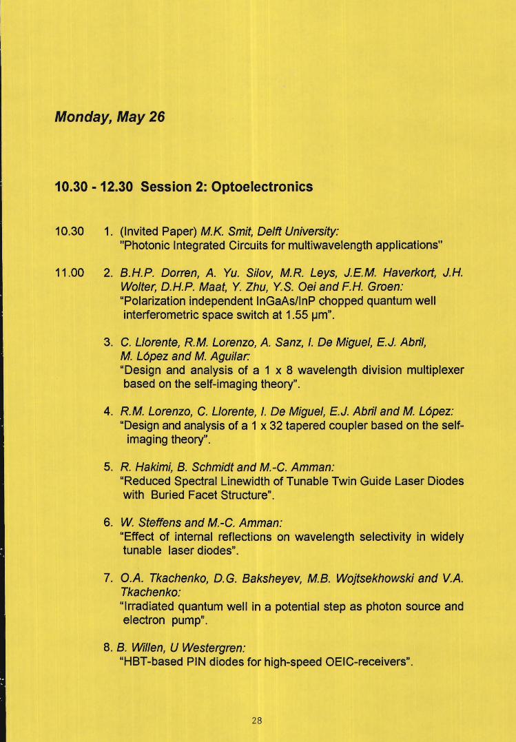
Monday, May 26
10.30 - 12.30 Session 2: Optoelectronics
10.30 1. (Invited Paper) M.K. Smit, Delft University:"Photonic Integrated Circuits for multiwavelength applications"
11.00 2. B.H.P. Do"en, A. Yu. Silov, M.R. Leys, J.EM. Haverkort, J.H.Wolter, D.H.P. Maat, Y. Zhu, Y.S. Oei and F.H. Groen:"Polarization independent InGaAs/inP chopped quantum wellinterferometric space switch at 1.55 IJm".
3. C. Llorente, RM. Lorenzo, A. Sanz, I. De Miguel, EJ. Abril,M. L6pez and M. Aguilar:"Design and analysis of a 1 x 8 wavelength division multiplexerbased on the self-imaging theory".
4. RM. Lorenzo, C. Llorente, I. De Miguel, EJ. Abril and M. L6pez:"Design and analysis of a 1 x 32 tapered coupler based on the self
imaging theory".
5. R Hakimi, B. Schmidt and M.-C. Amman:"Reduced Spectral Linewidth of Tunable Twin Guide Laser Diodeswith Buried Facet Structure".
6. W Steffens and M.-C. Amman:"Effect of internal reflections on wavelength selectivity in widelytunable laser diodes".
7. O.A. Tkachenko, D.G. Baksheyev, M.B. Wojtsekhowski and V.A.Tkachenko:"Irradiated quantum well in a potential step as photon source andelectron pump".
8. B. Willen, U Westergren:"HBT-based PIN diodes for high-speed OEIC-receivers".
28

Photonic Integrated Circuits for multiwavelength applications
Meint Smit and Yok-Siang OeiDelft University of Technology, Department of Electrical Engineering
P.O. Box 5031, 2600 GA Delft, The Netherlands
Toine StaringPhilips Optoelectronics
Prof. Holstlaan 4, 5656 AA Eindhoven, The Netherlands
Abstract. An overview is given ofadvanced photonic devices for multiwavelengthapplications and the potential and prospects ofphotonic integration are discussed.
1. Introduction
Optical communication is rapidly gaining importance. The explosive growth of services likeinternet requires both higher network capacity and network flexibility. Both can be providedby exploiting the wavelength domain as an additional dimension [1]. This is done in so-calledmulti-wavelength (MW or WDM, wavelength division multiplex) networks, wherewavelength is used for increasing link capacity as well as for signal routing.
MW-links and networks require optical components with an increased functionality. Photonicintegration is a key technology towards greater circuit complexity. Photonic IntegratedCircuits (PICs) that have been fabricated so far include multiwavelength receivers [2-6],multiwavelength lasers [7-11], and add/drop multiplexers [12,13]. The development of morecomplex integrated all-optical cross-connect circuits is progressing. When multiwavelengthnetworks become widely deployed, these devices are expected to gain a competitive edgeover discrete solutions.
In this paper a review is given of some work on PHASAR-based PICs for WDM applications,starting with a brief summary of the operating principle of a phased-array demultiplexer. Thefirst WDM systems are point-to-point connections using a number of different wavelengthchannels to increase the transmission capacity. Such systems will benefit from a PHASARdemultiplexer with integrated detectors which is discussed in Section 3, or a multiwavelengthlaser (Section 4 ). Network flexibility can be obtained by employing add/drop multiplexerPICs, as presented in Section 5. The article will be concluded with a discussion of theprospects and strategy for photonic integration.
2. PHASAR principle of operation
Figure 1 shows the schematic layout of a PHASAR-demultiplexer. When the beampropagating through the transmitter waveguide enters the Free Propagation Region (FPR) it isno longer laterally confined and becomes divergent. On arriving at the input aperture of thephased array the beam is coupled into the array and propagates through the individualwaveguides to the output aperture. The length of the array waveguides is chosen such that theoptical path length difference between adjacent waveguides equals an integer multiple of thecentral wavelength of the demultiplexer (as measured inside the waveguide). For this
29

wavelength the fields in the individual waveguides will arrive at the output aperture withequal phase (apart from an integer multiple of 2'1t), and the field distribution at the inputaperture will be reproduced at the output aperture. The divergent beam at the input aperture isthus transformed into a convergent one with equal amplitude and phase distribution, and animage of the input field at the object plane will be formed at the centre of the image plane.
The dispersion of the PHASAR is due to the linearly increasing length of the arraywaveguides, which will cause the phase change induced by a change in the wavelength tovary linearly along the output aperture. As a consequence, the outgoing beam will be tiltedand the focal point will shift along the image plane. By placing receiver waveguides at properpositions along the image plane, spatial separation of the different wavelength channels isobtained.
inputaperture
objectplane
transmitter
waveQuide
Figure la Schematic layout ofaPHASAR demultiplexer
TE TM .------
Figure Ib Microscope photograph ofan8x8 PHASAR demultiplexer /wavelengthrouter. The insets show the waveguidecross section (left) and an enlargement ofthe junctions at the array and at thereceiver side ofthe FPR (right). Chip sizeis 2.6 x 3.2 mm2
•
10
a>:!:. 15.... 20.9Q.:;:;L) 25C:a
30
35
1512 1516 1520 1524 1528 1532Wavelength (nm)
Figure Ie Filter response (superposition of8 channels) ofthe PHASAR shown above.
30

PHASARS have proven to be robust and fabrication-tolerant devices [14]. They areparticularly suited for integration with other active and passive components because they arerealised in conventional waveguide technology and require little or no additional processingsteps.
3. PHASAR-based multiwavelength detector
Fast, polarization-independent WDM receivers are key devices to upgrade high-capacitylinks. Figure 2a shows a photograph of a compact low-loss polarization-independent8-channel WDM receiver with 400GHz (3.2nm) channel spacing [6] . The upper part of thephotograph shows the PHASAR-demultiplexer, which was realized in conventional 2 11mwide, double-heterostructure ridge waveguides. The triangular region is included in order tocompensate the birefrengence of the applied waveguide structure (Figure 2b, left). Withoutcompensation the wavelength responses for TE and the TM-polarisation are shifted by severalnanometers, the so-called polarisation dispersion. In the triangle the InP top load has beenlocally removed (Figure 2b, right), thus increasing the birefringence. By properly shaping thecompensation region this increased birefringence compensates the polarisation dispersion ofthe rest of the array.
Figure 2b Waveguide structure outside(left) and inside the triangular dispersionregion (right)
108
Waveguide 2
4 6frequency (GHz)
2
-80
Figure 2a Photograph ofa PHASARdemultiplexer with integrated photodetectors. Full size is only 3.1 x 3.9 mm2•
Figure 2c Electrical response of thephotodetectors as a function ofthemodulation frequency.
31

The lower part of Figure 2a shows the detectors, which were fabricated in a twin-guidestructure with an absorbing InGaAs layer and a p-type InP top layer on top of the slightlyn-type doped transparent waveguide stack. As a first step, the absorbing top layer is removedby selective chemical etching, leaving small absorbing regions on top of the transparentwaveguide stack at the position of the detectors. In this way efficient detectors with lowcapacitance are realized. HF-response measurements show a 3dB channel bandwidthwell in excess of 10GHz (Figure 3c). On-chip loss of the device is 3dB for TE and 5dB forTM-polarization, the channel uniformity is better than IdB with negligible polarizationdispersion, and DC-crosstalk levels are lower than -40 dB (electrical). The residualpolarisation dispersion is almost negligible.
4. PHASAR·based multiwavelength laser
Complementary to the demultiplexer with integrated detectors is a multiwavelength laser, i.e.a laser source that can be operated at several wavelengths simultaneously. Two approacheshave been employed to reach this goal. The first is to integrate a DFB laser array with a starcoupler [7,8], the second is to use a wavelength-selective element within the laser cavity, e.g.an etched grating [9] or a phased-array wavelength multiplexer [10,11,15]
Figure 4a shows a photograph of a recently fabricated PHASAR-based multiwavelength laser[11]. The wavelength-selective element in the cavity is a PHASAR having a 400GHz(3.2nm) channel spacing, and a 38.75 nm free spectral range. Nine input waveguides areconnected to 500 Jlm long amplifier sections (the light regions at the right), while theremaining two are used for testing purposes. If one of the amplifiers is turned on, it will startemitting spontaneous emission which will be filtered by the PHASAR. After reflection at theoutput facet (left) it will come back in the amplifier. If the roundtrip gain becomes greaterthan one the device will start lasing at the maximum of the PHASAR passband. Figure 4bshows the output spectrum for simultanous operation of 4 wavelength channels.
02 3 4 5
-10
fii~
~ ·20.,c:$oS
-30
-401535 1540 1545 1550 1555
Wavelength (nm)
Figure 4a Photograph of the multiwavelength laser. Full size is only 3.5 x 2.5mm2
•
32
Figure 4b Spectrumfor simultaneousfour channel operation.

An important advantage of this type of laser is the fact that the channel wavelengths are set bythe multiplexer, so that no wavelength mismatch can occur between the laser source and themultiplexer. Another advantage is the very accurate channel spacing. Disadavantage is therelatively large cavity length (6 mm for the device shown in Figure 4a), which is a problem athigh modulation rates. Modulation speeds of 620 Mb/s have been succesfully demonstrated[15]. Although multiwavelength operation at very high bitrates is difficult the device has aninteresting potential as a discretely tunable laser in combination with an (integrated) externalelectro-absorption modulator: the channel spacing is much better defined than in DFB laserarrays. Linewidths in cw-mode are good: using a delayed self-homodyne technique, alinewidth of 21MHz has been observed.
5. PHASAR-based add/drop multiplexer
One of the key functions in WDM networks is to add and drop selected signals from thosepresent on a single fiber. The first add/drop multiplexers (ADM) have been realized insilica-on-silicon waveguides, integrating three PHASARs and 16 thermo-optical switches[12]. A compact (3x6 mm2
) reconfigurable InP-based integrated 4-channel ADM has beenreported recently [13], employing switches based on electro-optical phase shifting in aMach-Zehnder interferometer (MZn configuration, which allow for a very shortreconfiguration time.
The layout of this ADM is shown in Figure 5. It consists of a single PHASAR, integratedwith four loop-back paths containing the MZI switches. The input signal containing multiplewavelengths is led to the input of the PHASAR (right side) and multiplexed to the fouroutputs at the left side, which are fed to the four Mach-Zehnder switches on top of thePHASAR. In the off-state these switches couple the signals to their upper output ports whichare looped back to the PHASAR and multiplexed in the output port at the left, which is routedto the right side of the chip.
drop
700nm ~!1150nm300nm~
600nm i-InGaAsP(1.3)
Figure 5 Waveguide layout of the add/drop multiplexer. The upper part of the maskcontains the 4 MZI switches, while the lower part shows the PHASAR which is used as both ademultiplexer (the light travels from right to left) and multiplexer (the light travels in theopposite direction,from left to right). In addition a number oftest waveguides have beenincluded.
33

Or---.........,r---.........,r---___,~-___, O..---r----,---,.-----,
40 L:.:..:..:I:.:.:..:::.l..&o..~~.;.&....__....;.L.._'_"-'
1542 1546 1550 1554 1558
Wavelength (nm)
20 -----------.------------
30
lD 10~
IIIIII.20:c()
Co
15581554
(nm)
1546 1550
Wavelength
40 l-__...J.........L-_....L...--.L-'-'------'
1542
lD 10~
III
.Q 200:c()
co 30
(a)
Figure 6
(b)
Transmission spectrafrom (a) the input port to the output port, and (b) the inputport to the channel 3 drop port, with switch 3 on (solid) and off (dashed).
Figure 6 shows the performance of the device, with switching of channel 3 as an example.Two cases are shown: the signal on channel 3 is either dropped (switch 3 is on, solid lines), orpassed (switch 3 is off, dashed lines). The other channels are passed (i.e. switches off). Figure6a shows the transmission from the main input to the main output port. The total on-chip lossis only 10dB, which includes propagation loss through the PHASAR (twice), through theswitch (once), and through more than 2 cm waveguide length containing 3-9 waveguidecrossings.The dropped signal will be appear at the drop port (Figure 6b). Residual crosstalk inboth the main output port and the drop port is lower than -20 dB. It is limited by the switches.
6. Photonic Integration
The market for photonic integrated circuits, although rapidly growing, is still small. Forswitches and modulators integration has proven its value. For many applications, however,micro-optic, hybrid or fibre-based devices combine low cost with high performance andintegrated solutions are restricted to a few special applications so far.
A strong feature of photonic integration is reduction of packaging costs in circuits containingmany interconnected components. Figure 7 shows the scheme of an optical crossconnect withfour input and four output fibres, each of them carrying four wavelengths. It consists of fourinput demultiplexers, followed by an equalisr stage consisting of sixteen SOAs(Semiconductor Optical Amplifiers), four 4x4 switching matrices and four multiplexers formultiplexing the rerouted input signals to the four output fibres. If this component is realisedwith discrete planar components it requires more than one hundred fibre-chip connections. Ifit is realised in integrated form this number is reduced to eight!
34

-- ...:.: \
L...-_.....I \~":~ ~---14x~~:OO: ;'_!_... ""'. ,.--"..- "'" .......••••• "tI" - - ~ " : •••"---__ ,'.,.' 'j :: 1--_....
:=. ··)2:·~:~·:·~·:~4X~~::OO::/~// .:...... '.1'. ..... \,; ••••
1---....1 ... "'. % 1. :\ ... 1---....
-j:~\:::14 ~t:::OO:!.//\'-::.:::....:::::::: x::: :::::....::::.:1-__....1 L..__--'
Figure 7 Scheme ofa multiwavelength crossconnect consisting offour inputdemultiplexers, two interconnect networks, an equaliser stage with sixteen SOAs, four 4x4switch matrices and an output stage with four multiplexers. Total number ofcomponentsinvolved exceeds one hundred.
As can be seen from figure 7 circuits as complex as multi-wavelength crossconnects can becomposed of only three different components: (de)multiplexers, SOAs and optical switches.A technology capable of integrating these three components will be also be usable forrealisation of add-drop multiplexers (same components), multi-wavelength lasers (SOAs anda multiplexer) and, if the SOAs can be used as detectors by reversely biasing them, also formultiwavelength receivers. Such a technology may thus cover the demand for a broad varietyof components required in tomorrows photonic networks.
Two developments are presently speeding up the development of integration technology. Forthe first time a technology requiring devices with a high level of functionality,multiwavelength technology, is penetrating the network, thus creating a market to justifyinvestments in technology development.. Secondly, progress in epitaxial technology(MOCVD and CBE) makes it possible to grow selectively different structures in differentareas. In this way different devices can be optimised individually and the need to sacrificedevice performance to a practical integration scheme is strongly reduced. Modern integrationtechnology is, therefore, in a much better position for meeting system demands on deviceperformance and is expected to become a key technology for the photonic telecommunicationnetwork.
7. Conclusion
Multi-wavelength links and networks require devices with increased functionality ascompared to single-wavelength networks. Photonic integration of (de)multiplexers, switchesand SOAs has the potential to meet the demands on functionality, performance and costimposed by modern photonic networks, and will become a key technology if the rapid growthof multi-wavelength technology continues in the coming years.
Acknowledgements. Part of the work described has been funded by the European ACTSAC065 BLISS project.
35

References
1. CA Brackett, AS. Acampora, J. Sweitzer, G. Tangonan, M.T. Smith, W. Lennon, KC. Wang, R.H.Hobbs, "A scalable multiwavelength multihop optical network: A proposal for research on all-opticalnetworks", J. Lightw. Tech., Vol. 11 (5/6), pp. 736-753, May/June 1993.
2. C Cremer, N. Emeis, M. Schier, G. Heise, G. Ebbinghaus, and L. Stoll, "Grating spectrographintegrated with photodiode array in InGaAsPlInGaAs/InP", IEEE Photon. Techno!. Lett., vol. 4, pp. 108110,1992.
3. J.B. Soole, A Scherer, Y. Silberberg, H.P. LeBlanc, N.C Andreadakis, C Caneau, and KR. Poguntke,"Integrated grating demultiplexer and pin array for high-density wavelength division multiplexeddetection at 1.5 flm, Electron. Lett., vol. 29, pp. 558-560, 1993.
4. M.R Amersfoort, J.B.D. Soole, H.P. LeBlanc, N.C Andreadakis, A. Rajhel, and C Caneau, "8 x 2 nmPolarization independent WDM detector based on compact arrayed waveguide demultiplexer", Integr.Photon. Res. Topical Meeting (IPR'95), Dana Point, CA, February 23-25, Technical Digest Series, vol. 7,post-deadline papers, PD3.12, 1995.
5. CAM. Steenbergen, L.CN. de Vreede, C van Dam, T.L.M. Scholtes, M.K Smit, J.L. Tauritz, J.W.Pedersen, I. Moerman, B.H. Verbeek, and RG.F. Baets, "Integrated IGHz 4-channel InP PHASAR basedWDM-receiver with Si bipolar frontend array", Proc. 21th Eur. Conf. Optical Commun. (ECOC'95),Brussels, September 17-21, vol I, pp. 213--214,1995.
6. CAM. Steenbergen, C. van Dam, A Looijen, CG.P. Herben, M. de Kok, M.K. Smit, J.W. Pedersen, I.Moerman, RG. Baets, and B.H. Verbeek, "Compact low-loss 8 x 10 GHz Polarization independentWDM Receiver", Proc. 22nd Eur. Conf. Optical Commun. (ECOC'96), Oslo, September 15-19, vol. 1,pp. 129-132, 1996.
7. CE. Zah, FJ. Favire, B. Pathak, R. Bhat, C Caneau, P.S.D. Lin, A.S. Gozdz, N.C Andreadakis, M.AKoza, and T.P. Lee, "Monolithic integration of multiwavelength compressive-strained multi-quantum welldistributed-feedback laser with star coupler and optical amplifiers, Electron. Lett., vol. 28, pp. 2361-2362,1992.
8. M.G. Young, U. Koren, B.I. Miller, M.A. Newkirk, M. Chien, M. Zirngibl, C. Dragone, B. Tell, H.M.Presby, and G. Raybon, "A 16xl wavelength division multiplexer with integrated distributed Braggreflector lasers and electroabsorption modulators, IEEE Photon. Technol. Lett., vol. 5, pp. 908-910, 1993.
9. K.R. Poguntke, J.B.D. Soole, A Scherer, H.P. Leblanc, C Caneau, R. Bhat, and M.A Koza,"Simultaneous mUltiple wavelength operation of a multistripe array grating integrated cavity laser", Appl.Phys. Lett., vol. 62, pp. 2024-2026, 1993.
10. M. Zirngibl and C.N. Joyner, "12 frequency WDM laser based on a transmissive waveguide gratingrouter, Electron. Lett., vol. 30, pp. 701-702, 1994.
II. A.A.M. Staring, L.H. Spiekman, JJ.M. Binsma, EJ. Jansen, T. van Dongen, PJ.A Thijs, M.K. Smit, andB.H. Verbeek, "A compact nine-channel multiwavelength laser, IEEE Photon. Technol. Lett., vol. 8, pp.1139-1141,1996.
12. K. Okamoto, M. Okuno, A Himeno, and Y. Ohmori, "16-channel optical add/drop multiplexer consistingof arrayed-waveguide gratings and double-gate switches, Electron. Lett., vol. 32, pp. 1471-1472, 1996.
13. C.G.M. Vreeburg, T. Uitterdijk, Y.S. Oei, M.K. Smit, F.H. Groen, n.G.M. van der Tol, P. Demeester,and H.J. Frankena, "First InP-based reconfigurable integrated add-drop multiplexer", IEEE Photon.Technol. Lett., vol. 9, pp. 188-190, 1996.
14. M.K Smit and C. van Dam, "PHASAR-based WDM devices: principles, design and applications", J. ofSel. Topics in Quantum. Electron., Vol. 2, No.2, pp. 236-250, June 1996.
15. M. Zirngibl, "Multifrequency Lasers for Dense WDM Application", Proc. 8th Eur. Conf. On IntegratedOptics ECIO '97, Stockholm, Sweden, April 2-4, 1997, pp. 254-259.
36

Polarization independent InGaAslInP chopped quantum wellinterferometric space switch at 1.55 IJm.
B.H.P. Dorren, A.Yu. Silov, M.R. Leys, J.E.M. Haverkort and J.R. Wolter, COBRAInteruniversity Research Institute, Physics Department, Eindhoven University of Technology,P.O. Box 513, 5600 MB Eindhoven, the Netherlands.D.H.P Maat, Y. Zhu, Y.S. Oei and F.H. Groen, Department of Applied Physics, Delft Universityof Technology, P.O. Box 5031, 2600 GA Delft, the Netherlands.
Abstract:A Mach-Zehnder Interferometric (MZI) space switch using a novel CRE grown InGaAsnnPchopped quantum well (CQW) phase section is presented. Each CQW consists of three 3IA.InGaAs strained quantum wells separated by 12.4. InP barriers. This structure shows a shift ofthe absorption edge as high as 80nm at lOY reverse bias. The heavy hole and light holesubbands cross at approximately 0.6% tensile strain. Using these chopped quantum wells, werealized MZ/'s with low attenuation and a V2.l product as low as 3.6 V2.cm. Finally, we realizedfull polarisation independent switching using 0.75% tensile strained CQW's.
A first constraint for the design of a MZI space switch at 1.55 11m is waveguide transparancy.When using tuning sections based on the Quantum Confined Stark Effect (QCSE) withInGaAslInP quantum wells, the QW-thickness is limited to a maximum of 40A for preservingwaveguide transparancy. Such a small QW-thickness is far from optimum for an appreciableQCSE. Chopped quantum wells allow to combine waveguide transparancy at 1550 nm with alarge bandgap shift. We have grown three CQW samples consisting of 20 CQW's, each withthree strained 31A InGaAs QW's separated by 12A InP barriers (See Fig. 1). The CQW's areembedded into a p-i-n structure. A cross-sectional view of the structures is depicted in figure 1.
n-1nPSlbslrale
20x
Fig l: A cross-sectional view of the MZI-tuning section using chopped quantumwells.
We have grown CQW's with a tensile strain of 0.43%,0.55% and 0.75% within the wells toobtain polarisation independent switching. Fig. 2a shows the effective red shift of the lowestconfined energy state under applied bias of the sample with 0.43% tensile strain. Red shifts ashigh as 80nm at 10V applied bias are observed. Fig. 2b shows the effective absoprtion edges forTE and TM polarization as obtained by cleaved-side photocurrent measurements at 4K. Weobserve that the heavy-hole and light-hole subbands cross around 0.6% tensile strain.
37
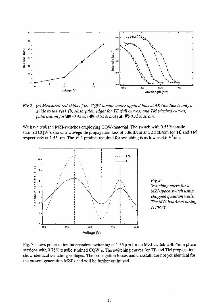
13501325
wavelength (nm)
13001275
2.0
0.0 c.....J._---'-_.....L-_.........:._...L-_-'--_L.-----..--::l
6.0
8.0
10
Voltage (V)
20
120,.-----------------,
100
II 80
.s~ 601Il"0
ti 40
Fig 2: (a) Measured red shifts ofthe CQW sample under applied bias at 4K (the line is only aguide to the eye). (b) Absorption edgesfor TE (full curves) and TM (dashed curves)polarizationfor(1I) -0.43%, (_) -0.55% and (~, ~-0.75% strain.
We have realized MZI-switches employing CQW-material. The switch with 0.55% tensilestrained CQW's shows a waveguide propagation loss of 3.8dB/cm and 2.5dB/cm for TE and TMrespectively at 1.55 ~m. The V2.z product required for switching is as low as 3.6 V2.cm.
7,---------.-----....,----T"'""""""-----,
Fig 3:Switching curve for aMZI-space switch usingchopped quantum wells.The MZI has 4mm tuningsections.
10.07.5
--- --- TM
--TEIIIIIIIII
-rI'" , \. ...
/ \I \, ,
I ', '.,,,
/I
/I,
//
/, , ,\ I /.r
II
5.02.5
III
... .1 ...... ,
/ '/ \
/ \, \
/ \
I ', \, \, \
/ \, ,, \, \
/ ', \, \
, ', '.,,,,
I,/
/,,/
"
0.0
6
~ 5~Q)
19 4III
~D
.£ 3Z'iiicQ) 2E
Voltage (V)
Fig. 3 shows polarization independent switching at 1.55 ~m for an MZI-switch with 4mm phasesections with 0.75% tensile strained CQW's. The switching curves for TE and TM propagationshow identical switching voltages. The propagation losses and crosstalk are not yet identical forthe present generation MZI's and will be further optimized.
38

DESIGN AND ANALYSIS OF A lx8 WAVELENGTH DIVISION MULTIPLEXER
BASED ON THE SELF-IMAGING THEORY
C. Llorente, R.M. Lorenzo, A. Sanz*, 1. de Miguel, EJ. Abril, M. Lopez and M. Aguilar*
Departamento de Teona de la Senal, Comunicaciones e Ingeniena Telematica
E.T.S.I. Telecomunicacion, cl Real de Burgos sin, 47011 Valladolid - SPAIN
Tfno.: +34 83 - 423260, Fax: +3483 - 423261, e-mail: [email protected]
(*)Departamento de Teona de Tecnologia Electronica, E.T.S.I.T. - U.P.M.
The property of multimode waveguides of reproducing an input field in multiple
(or single) images at intervals periodically spaced (self-imaging theory) has been applied
into the study of optical devices. Concerning to this, the method of analysis in which the
propagation of each mode is studied and, eventually, the output field is calculated by
means of the recombination of the propagated mode fields, is called multimode
interference (MMI) [1]. This theory drives to practical devices like couplers [2], splitters
[3] and switches [4] that have been developed so far. The reason why is that MMI
technology improves features like cost savings, lower dimensions, better manufacturing
tolerances and simple fabrication. Polarisation changes transparency and simple design
criteria are additional goals for these devices.
Wavelength division multiplexing (WDM) is the way to increase the optical fibres
transmission capacity, and several works have been done [5] in order to get as much
channels as possible in the field of broadband telecommunication networks [6]. Several
numerical techniques has been used to analyse dielectric waveguiding problems, and the
beam propagation method has become one of the preferred solutions [7].
In this paper, we have analysed a Ix8 wavelength division multiplexer, by means
of the self-imaging effect, and so it could be called a MMI coupler. Our design is novel as
far as we have reduced its dimension without any penalty in other feature, reducing both
computing time analysis and future fabrication costs. 8 are the number of channels chosen
to work with, running from 1.538 to 1.552 J..l.m, and the cladding, nc, and core, nr,
refractive index are 1.445 (SiOJ and 1.473 respectively. So weak guiding glass
waveguides with step refractive index profile are about to use.
This device can be easily decomposed in three different stages and two of them
are MMI devices. The middle section only works carrying the signal from the input to the
output sections (see Figure 1).
39

------------------------
I,,I
\-~,
l-i I ,'~-- -,/ // /~ . C
i, .. / I//'\~ ,I , L,
J / / ./ '\, \---i
r- I
r- ,//r~\i-- ,
l-- , it ..... \~ "I,L.- \ , I , --i
L '1/ I '\ -Ji \
I;~ '~Ir-- , ---4I -jr---- \ /~j \~ ~~ I -j
t= ,
lI " 'I -lI
L-/,
;I // ---", /-
I .'\ /u
---------------------Figure 1. Structure of our design, in which the three different stages can be easily seen since a zoom
has been done.
The input section is a Ix8 power splitter, and its dimension can be reduced if only
the even modes are excited at the input by the mechanism called symmetric interference. 8
equally spaced images are obtained at the output of the fIrst section. The output MMI
element is a 8x8 splitter, in which its 8 input are combined to get constructive interference
in order to drive the field distribution to one and only one output. The key parameter inthis combiner is the input signals phase [8], and this is the task for the middle section. The
phase differences conditions to get constructive intP.Jference can be shown in the Table I.
The phase of the field which has traveled through each waveguide depends on the
waveguide length and so, this length is what we have to play with.
Table 1: Phase conditions to be satisfied at the input of the second MMI device to get constructiveinterference at the desired output. Only these data are needed because of the theoretical symmetry.
0\1 1 2 3 4 5 6 7 88 7t -77t/8 7tl8 7tl2 -7t/2 7tl8 -77t/8 07 7t 7tl2 7tl8 7tl8 -7t/2 06 7t 7tl8 7tl8 05 7t 0
[I] L.B. Soldano and E.CM. Pennings, J. ofLigthwave Technol. 13 (4), 615 (1995).[2] P.A. Besse, M. Bachmann, H. Melchior, L.B. Soldano and M.K. Smit, J. Ligthwave
Technol. 12 (6), 1004 (1994).[3] A. Ferreras, F. Rodriguez, E. Gomez-Salas, J. L. Miguel and F. Hernandez-Gil, IEEE
Photon. Techno!. Lett. 5 (10), 1224 (1993).[4] J.E. Zucker, 1(. L. Jones, T.H. Chiu, B. Tell and 1(. Brown-Goebeler, J. of Ligthwave
Technol. 10 (12), 1926 (1992).[5] L. O. Lierstuen and A. Sudbe, IEEE Photon. Technol. Lett. 7 (9), 1034 (1995).[6] S.S. Wagner and H. Kobrinski, IEEE Commn. Magazine, (March), 22 (1989).[7] P.E. Lagasse and R. Baets, Radio Science, 22 (7), 1225 (1987)[8] M. Bachmann, P.A. Besse and H. Melchior, Applied Optics, 33 (18), 3905 (1994).
40

DESIGN AND ANALYSIS OF A lx32 TAPERED COUPLER BASED ON THE
SELF-IMAGING THEORY
R.M. Lorenzo, C. Llorente, I. de Miguel, EJ. Abril and M. Lopez
Departamento de Teoria de la Sefial, Comunicaciones e Ingenieria Telematica
E.T.S.I. Telecomunicacion, cl Real de Burgos sin, 47011 Valladolid - SPAIN
Tfno.: +34 83 - 423260, Fax: +34 83 - 423261, e-mail: [email protected]
A theoretical and practical development of the Multimode Interference
Technology (MMI) has been carried out lately. This theory drives to practical devices like,
for instance, couplers [1], splitters [2], [3], wavelength division multiplexers [4) and
switches [5] that have been developed so far. The reason is that MMI technology improves
features as cost savings, lower dimensions, better manufacturing tolerances and simple
fabrication. Polarisation changes transparency and simple design criteria are additional
goals for these devices. The MMI technology main drawback is that couplers tend to be
large if we are trying to get low loss and high accurateness when signals are driven out to
our clients.
The number of clients, users of these optical communication networks, are
currently rising. It is within this context in which we locate our paper. We will design a
device that splits an optical signal in 32 output channels both reducing dimensions and
improving features.
With this paper, we aim to show that it is possible to reduce the rectangular
splitters dimensions and improve their characteristics, controlling the excited number of
modes with an appropriate taper. In order to simulate the present devices behaviour, order
oand order 2 ftnite differences BPM have been used.
A I-by-32 coupler will be design for the third telecommunication window, i.e., a
wavelength, A, of 1.55 IJm. The material we have worked with is Si02 (nr=1.445). We
carried out the design with weakly guiding glass waveguides with a step refractive index
profIle equal to 0.005.
Traditionally power splitters have used a rectangular waveguide as MMI section,
as shown in Figure 1.(a). When we wish to distribute the signal to a high number of
outputs, the size of the former design becomes a problem. Tapered design illustrated in
Figure l.(b) will reduce dimensions without penalty in the features couplers.
41

c::::==c::::== (a)c::::==
Inputmonomodewaveguide~
OutputMMI monomode
Jection...wa~eguides------,
.. ~.. ... .. ......-..Input Output Taper
monomode MMI section monomodewaveguide waveguides
Figure 1. Geometry of two MMI power splitters. (a) Classical coupler using a rectangular MMIsection. (b) Coupler using a taper to drive the input signal to the MMI waveguide.
Every dimension have been optimised and several parameters studied. Table 1
show the result of this work. Among others, wavelength influence, fabrication tolerances
and bandwidth are to be highlighted.
Table 1. Summary of the parameters of I-by-32 rectangular and tapered couplers.
Rectangular coupler Tapered couplerDevice width 7750 J.lm 7750 J.lmDevice length 31106 11m 24106 11mExcess losses 0.8 dB 0.51 dBUniformity 1.13 dB 0.44 dBTaper length tolerance - ±105 1lmTaper width tolerance - ±50 11mMMI section length tolerance ±115 11m ±115 J-lmMMI section width tolerance ±3 J.lm ±311mWave reflected energy -55 dB <-55 dBUniformity polarisation dependence 0.20 dB ~OdB
Excess losses polarisation dependence 0.09 dB 0.03 dBBandwidth ±15nm 49nm
[1] P.A. Besse, M. Bachmann, H. Melchior, L.B. Soldano and M.K. Smit,1. LigthwaveTechnol. 12 (6), 1004 (1994).
[2] A. Ferreras, F. Rodriguez, E. Gomez-Salas, 1. L. Miguel and F. Hernandez-Gil, IEEEPhoton. Technol. Lett. 5 (10), 1224 (1993).
[3] T. Rasmussen, J. K. Rasmussen and J0m Hedegaard Povlsen, J. of LigthwaveTechnol. 13 (10), 2069 (1995).
[4] L. O. Lierstuen and A. Sudba, IEEE Photon. Technol. Lett. 7 (9), 1034 (1995).[5] J.E. Zucker, K. L. Jones, T.R. Chiu, B. Tell and K. Brown-Goebeler, J. of Ligthwave
Technol. 10 (12), 1926 (1992).[6] RUlrich and T. Kamiya, 1. Opt. Soc. Am. 68 (5), 583 (1978).
42

Reduced Spectral Linewidth of Tunable Twin Guide LaserDiodes with Buried Facet Structure
R. Hakimi: B. Schmidt* and M.-C. Amann
Institute of Tuhnical Elfctronics, University of Kassd,Heinrich-Pldt-Str. 40, D-34132 Kassd, GermanyTel.: ++49561 804-4103, Fax ++49 561 804-4488
* Siemens AG, Corporate Research and Development,Otto-Hahn-Ring 6, D-81739 Miinchen, Germany
Electronically wavelength tunable single mode laser diodes are key components for advanced photonic applications [1,2J. An advanced type of continuously wavelength tunablelaser diode requiring only one tuning current is the 1,551lm InGaAsPfInP tunable twinguide (TTG) laser [3]. As with other electronically tunable laser diodes: the TTG laserexhibits an excess linewidth broadening during tuning [4]. This broadening is due tocarrier density fluctuations caused by noise processes in the tuning region which lead torefractive index fluctuations~ that finally result in an excess linewidth broadening. Theorigin of carrier density fluctuations in the tuning region and their effect on linewidthbroadening has already been described in [5 - 7]. In this paper we demonstrate for thefirst time: that the linewidth broadening in TTG laser diodes can significantly be reducedby Qurying the facets of the TTG laser (BF-TTG-Iaser).
Both the spectral density of the voltage noise at the terminals of the tuning diodeand the spectral density of the FM noise indicate a significant Iff carrier noise of upto several hundred kHz which is essentially caused by surface recombination at the laserfacets. It has been shown that the Iff carrier noise in heterostructure laser diodes cansignificantly be reduced by facet passivation with sulphur [8J. This noise reduction isclearly attributed to the temporary removal of surface states by the sulphur passivation[5J. A permanent removal may be achieved by entirely burying the tuning region ofInGaAsPfInP TTG laser diodes within InP. Fig. 1 schematically shows the longitudinalsection of this BF-TTG laser structure. The thickness of the InP window at the facets is
5IJrn
Figure 1: Longitudinal section buried facets tunable twin guide (BF-TTG) laser.
43

L\f =1 kHz
5pm. As active and tuning layers are completely embedded in high-bandgap InP: surfacestates are essentially excluded. Due to the lacking surface recombination the carrierdensity fluctuations in the active and the tuning region significantly decrease.
Fig. 2 displays the spectral density of noise power at the terminals of the tuningdiode of TTG lasers with and without InP-windows in the frequency range from 1 kHzto 10MHz. As can clearly be seen: the BF-TTG laser shows a distinctly lower noiselevel. At a tuning current of 5 rnA (500 A/cm2
) we obtain a reduction in noise power ofabout 15 dB at 1 kHz. In accordance with the noise reduction in the tuning region thespectrallinewidth broadening was also drastically reduced. Therefore the BF-TTG laserwith InP-windows exhibits a linewidth reduction by about 10 MHz as compared with theprevious TTG laser at a tuning current of 5 rnA.
E -50en"0 • __
; -60 - ....,. without buried facets'00 --.~.c -.__•~ -70~..... .....-.-.... ""'.~ -......~ ".o -80- ~.......... '.
~ with buried face~.....&......'0 -90 ....- ........- ..z .
0,001 0,01 0,1 1 10Frequency (MHz)
Figure 2: Spectral density of noise power at the tuning diode terminals of TTG laser withand without buried facets.
[1] K. Kobayashi and 1. Mito: IEEE J. Lightwave Technol. 6: 1623 (1988).[2] T. L. Koch and U. Koren: IEEE J. Lightwave Techno!. 8: 274 (1990).[3] M.-C. Amann and S. Illek: IEEE J. Lightwave Technol. 11: 1168 (1993).[4] Y. Kotaki and H. Ishikawa: IEEE J. Quantum Electron. 25: 1340 (1989).[5] M.-C. Amann: et. al.: to be published in Appl. Phys. Lett.[6] B. Tromborg: et. al.: IEEE J. Quantum Electron. 27: 178 (1991).[7] M.-C. Amann and R. Schimpe: Electron. Lett. 26: 279 (1990).[8] R. Hakimi and M.-C. Amann: unpublished.
44

Effect of internal reflections on wavelength selectivityin widely tunable laser diodes
W. Steffens and M.-C. Amann, Institute ofTechnical Electronics,University of Kassel, Heinrich-Plett-Str. 40, D-34132 Kassel
Abstract: A key issue in widely tunable lasers is the number of accessible wavelengthchannels. Typically only 25% of the available cavity modes can be accessed [1]. This paperinvestigates the suppression of individual modes by internal reflections caused by the indexperturbation of a codirectional coupling grating and the improvement by applying a taperedgrating structure.
Introduction: Tunable semiconductor lasers are key devices for advanced photonicsystems in optical communications, measurement and sensing. Among the various laserstructures presented so far, the devices with codirectional mode coupling [1, 2, 3] offer theadvantage of requiring only one single control current for tuning. Wide wavelength tuningof up to 74.4 nm with side-mode-suppression-ratio (SMSR) of> 25dB has been reported.However, typically at most -25% of the available modes can be accessed (1]. An essentialorigin of the unsatisfactory wavelength access represent the multi-mirror-effects caused byinternal reflections at the grating.
WG2
WG1
Fig. 1: Schematic longitudinal section ofa verticalcoupler filter (VCF) for codirectionalcoupling between modes Rand S.
Device Structure: Fig. 1 illustrates thetwin-guide structure of a vertical couplerfilter (VCF). The twin waveguide structuresupports two transverse modes whichexhibit a clear spatial separation essentiallyconfined either in WGI (mode R) or inWG2 (mode S). Coupling between the twocodirectionally propagating modes isaccomplished by the grating with gratingperiod A (typically 10-20 Jlm). A maximumcoupling efficiency is achieved atwavelength Ao == A 6.nei1 ' where 6.ni{tl is the
difference of the effective refractive indicesof the two modes R and S. The structureenables the selective refractive index change by local index variations within one of thewaveguides. Thus, tuning can be achieved by adjusting the refractive index of one of thewaveguide modes [2]. To study the longitudinal mode selectivity, we assume a laser withvariable total length LT and a constant coupler length of Le = 600 ~m yielding a completecoupling between modes Rand S at the filter wavelength. For comparison we consider anideal cavity design with Le/LT = 1 and a realistic one with Le/LT = 0.5 [4]. Longitudinalmode spacing is 0.57 urn and 0.28 nm, respectively.
Calculations: The codirectional coupling of modes R and S and the backward reflections atthe periodic perturbations are taken into account by a 4 X 4 transfer matrix for each period.The power transfer through the coupler and the reflected power in mode R and S can bemodelled by multiplying the transfer matrixes of all periods. Owing to the fabricationtolerances of at least 0.1 Jlm the reflections at the numerous perturbations exhibit randomphase and are therefore not phase-matched at any wavelength [5]. Simulations have beencarried out assuming an effective refractive index of 3.3 for mode R and an effectiverefractive index difference between modes R and S of 0.1. The end mirror reflection
45

coefficient is taken to be 0.3. The resulting effective filter transfer functions for twodifferent tuning currents are displayed in Fig. 2a. Evidently the filter transfer function isdisturbed by backward reflections at the periodic perturbations. The longitudinal modewith the maximum power transmission through the VCF exhibits the lowest threshold gain.It also can be seen from Fig. 2a that the filter transfer function consists of an ideal filtercurve and, due to the random phase distribution, a superimposed corrugation. Duringtuning, the ideal filter curve is shifted whereas the corrugations are fixed for eachwavelength deviation. These corrugations may suppress or enhance individual modes. Atwavelengths with local minima (see arrows) no longitudinal modes can be accessed. So,the existence of internal reflection affects the number of accessible modes but also the sidemode suppression ratio.
1.0 100'" -e- L" I LT = 1(/)
OJe~ -.- L" I LT = 0.5c "0 80
.Q 0(/) ~
\ e~(/) -.~ 0.9 060~
OJ
~ e,----c .0en E~ ::l 40
e ___e
z ..............---.-.0.8_6 -4 -2 0 2 4
200.0 0.2 0.4 0.6 0.8 1.0
A.-A.. ~ = r(cp) I reO)a) b)
Fig. 2: a) VCF Filter curves for two different tuning currents. The doted lines indicate the idealized casewith no internal reflections. b) Number of accessible modes against power reflection ratio ~ oftapered grating.
Improvement of Wavelengtlt Access: A significant reduction in backward reflectionwithout affecting the codirectional mode coupling can be obtained by lateral tapering of theindex perturbations [5]. The reduction in reflection is measured by the power reflectionratio'; = r(rp)/r(O) which relates the reflection of the tapered transition r(rp) with that of thenon-tapered structure r(O), where rp is the slant angle. A reduction by more than two ordersof magnitude is possible for typical device structures without affecting the codirectionalcoupling. The number of accessible modes of the studied device is plotted against'; in Fig.2b. It can be seen that a reduction in parasitic reflections strongly increases the number ofaccessible modes.
Conclusion: The wavelength selectivity of widely tunable lasers utilizing a VCF has beenstudied. Depending on the statistical phase distribution of the internal backward reflections,constructive or destructive interference occur and thus may randomly corrugate the filtercurve. The corrugation may randomly suppress individual modes and restricts the numberof accessible modes.
References(1] KIM. I. et al., Appl. Phys. Lett., 1994,64, pp. 2764-2766[2] AMANN, M.-C. et aI., 1993, LT-ll, pp. 1168-1182[3] RIGOLE, P.-l. et al., Electron. Lett., 1996,32, pp. 2352-2354[4] ALFERNESS R. C. et aI., Appl. Phys. Lett., 199,60, pp. 3209-32 I I[5] AMANN, M.-C. et al., Electron. Lett., 1996,32, pp. 221-222
46

Irradiated quantum well in a potential stepas photon source and electron pump
O.A. Tkachenko, D.G. Baksheyev, M.B. Wojtsekhovski, VA Tkachenko·Novosibirsk State University, Novosibirsk, 630090, Russia
• Institute of Semiconductor Physics, Novosibirsk, 630090, Russia
Inelastic resonant electron transmission through semiconductor triple-barrier asymmetricstructures [1) and Stark superlattices [2] has recently been predicted to be almost full due tophoton-induced transitions between two or more quasi levels. In this report we will show thatanalogus strong response to irradiation can be produced by the structure in which electrontunneling in elastic channel is absent and which possesses only one quasilevel. Analyticsolution for the time-periodic Schriidinger equation with potential in the form of a sharpstep with o-well placed at the higher potential side gives the Breit-Wigner-type formula fortransmission coefficient with emission of quantum nw:
f.f,T-, = Tonax (E _ nw - Eo - oEo)2 + ~(f. + fY'
where E is the energy of the electrons incident from the higher potential side, Eo and f. thequasilevel and its width in the absence of hffield, oEo and f, the shift and broadening of thequasilevel due to inelastic decay, r. being proportional to the square of hf field amplitude.Thus, one can control the probability of inelastic transitions by varying frequency nw andirradiation intensity. When f, = f. the inelastic transmission coefficient, at the resonanceE = nw + Eo + oEo, reaches its maximum T_ I = T,nax. Analytic treatment and numericalmodeling of real structures show that T,,,.x can be close to unity at relatively small amplitudesof hf fields.
Such configuration can be made of an n-Gao.6sAlo.3sAs/GaAs/Gao.6sAlo.3sAs/n-GaAsstructure with the voltage applied to its doped contacts to prevent from band bending[Fig. I(a)]. Alternating voltage is provided by monochromatic infrared irradiation polarized along the growth direction of the structure. Numerical calculations show that 70%transmission with emission of photons occurs in such structure, at optimized barrier thickness, frequency and amplitude of the high-frequency field, when cold electrons of energy Efall onto the quantum well from the higher potential side of the structure. ';Vith the accountof elastic channel the transmission becomes almost full (95%) whereas it is small (4%) in theabsence of irradiation [Figs. l(b), I(cll.
Stacking such well-in-step configurations in a single heterostructure permits of makinga tunable cascade-amplifier of irradiation, and in this case inevitable technological nonuniformities of the cascades and deviating positions of quasilevels will not impede its workability. Indeed, since the electron motion above the step is classically allowed the energy ofincident electron and, respectively, the frequency of the hf field are more widely variable thanin resonant photon-assisted tunneling throngh two quasilevels Eo and E, of an asymmetrictriple-barrier structure [1]. In the former case the only resonant condition E = Eo+nw musthold instead of two conditions in the latter case: E = Eo, E, = Eo -nw. It differs advantageously from single-well [3] and multiple-well [41 cascades in which photon must couple thepairs of quasidiscrete states.
Due to detailed balance, an analogous p-i-n structure with an InrGal_rAs quantum wellcan act, at a corresponding direct voltage, as an electron pump for electrons incident on thepotential step from n-GaAs side and having the energy of the quasilevel.
47

o
300E-- -
--&-
hf on
hf off-
- (a)'--
J!..(x) -I I
o
3
-3
0 x (nm)10 20
(b) Ttotal (c) Ttotal
T.1
T. 1
To
0 0
176 hv(meV) 179 0 &(m V Inm) 10
Figure 1. (a) Time-averaged probability density 1\lII2 and potential of the structure U(x).Electrons of energy E = 320 meV are incident from the left. Switching on hf field (hw =177.5 meV, amplitude £ = 5 IIIV/nm) results in strong increase of transmission. (b) Frequency dependence of elastic, To, inelastic, T_ t , and total transmission at fixed amplitude£ = 5 mV/nm. (c) Transmission at resonant frequency liw = 177.5 meV versus amplitudeof hf field.
References
[lJ M. Vu. Sumetskii and M. L. Felshtyn, Pis'ma Zh. Eksp. Teor. Fiz. 53(1), 24 (1991);C. A. Stafford and N. S. Wingreen, Phys. Rev. Lett. 76 1916 (1996).
[2] O. A. Tkachenko, V. A. Tkachenko, and D. G. Baksheyev, J. Appl. Phys. 81(4), 15February 1997; O. A. Tkachenko, V. A. Tkachenko, D. G. Baksheyev, and A. S. Jaroshevich, in Compound Semiconductors-95, lnst. Phys. Conf. Ser. No 145 (lOP, 1996),Chapter 10, pp. 119:3-1198.
(3] R. F. Kazarillov, R. A. Suris, SOy. Phys. Semicond. 6, 120 (1972).
[41 J. Faist, F. Capasso, C. Sirtori, et al., Appl. Phys. Lett. 64, 1144 (1994).
48

HBT-based PIN-diodes for high-speed OEIC-receiversBo Willen and Urban Westergren
Department ofElectronics, Royal Institute ofTechnologyS-164 46 Kista, Sweden
o
0.2
~c
0.8 IE~
0.4 ~a
0.8
5
2 x 10 um
5K 10 um
2 3
l-layarthlckn... [um]
Ol------r---,-----,-----r------i
o
20
80
100 ,-,.--------------, 1.0
IntroductionThe growth and spread of the information society continue to increase, and new telecommunicationservices are emerging. The resulting requirements for an increased capacity of the transmissionsystems can be met by increased time, wavelength, or space multiplexing. These techniques are notexclusive, but it is of decisive importance that the limitation of each one is determined. When timemultiplexing is used for fibre optical transmission, the limitations are optical dispersion and themaximum bandwidth of the optoelectronic interfaces, that is, the transmitter and the receiver. Thebandwidth of an optoelectronic transmitter is mainly governed by the high-frequency properties ofthe light-emitter itself, and a hybrid solution with a separate driver is therefore competetive with themonolithic counterpart. In contrast to this,a receiver benefits substantially frommonolithic integration regarding sensitivityand bandwidth, and is today the mostfrequent developed DEIC.Fig. I. Bandwidth and quantum efficiencedependence ofthe collector Width for an HBTbased PIN-diode.
It has become a common technique toemploy the base-collector-subcollectorregion of an InP-HBT as a PIN-typephotodetector used in DEIC-receivers. Thismeans that the collector thickness must bedesigned regarding the photodetectorresponse. Both the amount of detectedphotons and the time required to get thegenerated charge carriers out of the activearea increases with the absorption depth, sothe optimum choice is a tradeoff betweenquantum efficiency and bandwidth, as shown in Fig. 1. High-speed detectors require a thin i-layer,so the absorption in the underlaying subcollector is significant. The shown transit time delay istherefore valid only if the effects of slow carriers diffusing from the subcollector region can beneglected. This is achieved by including a properly graded heterojunction in the collector-subcollectorinterface to create an effective hole barrier in the valence band.
Fig.2. EqUivalent model for anHBT-based PIN-diode.
An HBT-based photodetector differs significantly from aconventional pin-diode, the main difference being thethickness ofthe base layer in an HBT that is made extremelythin to enhance the high-speed properties. When used as thep-layer in a pin-diode, the thin layer results in a high seriesresistance, making the conventional model that consists ofaseries resistor and a leakage resistor in parallel with acapacitor inadequate: The frequency dependence of
49

evaluated PIN-diodes cannot be explained by a single pole equivalent. This can be understood sincea part of the i-layer situated sufficiently close to the p-contact does not suffer from the high serialresistance in thep-Iayer because the holes will drift directly towards the contact, while the central partis strongly affected from this resistance since the holes must traverse a significant part of the p-Iayer.This effect is especially pronounced for wide active areas. The distributed base resistance isapproximated as the single intrinsic resistance R] in Fig.2.
Further, the active part shaded by the contact metal must be separated out to allow for an adequateinput signal area. Thus the device area needs to be partioned into three separate regions, one passiveregion below the contact metal, one low resistive active region close to the contact, and one highresistive active region in the centre of the device. The resulting extended equivalent small-signalmodel shown in Fig.2 is found appropriate in our simulations, and it also strongly shows theimportance ofusing a circular base contact to decrease the effect of the high base resistance.
The implication of the thick collector layer on the RBT performance is a decrease in the basecollector capacitance, Csc. It also makes C Bcbias dependent, as shown in Fig.3, since the widecollector not is depleted at zero bias. The maximum frequency of oscillation, fmax, increases over theentire bias range, while the transit frequency, fn is almost constant, so the t:nax-to-fT ratio is almostthree at a high bias. The base-collector time delay Be = f/(8 fma/) = RB CBC is also ploted in the figureand displays the rapid decrease in the capacitance, assuming a constant base resistance.
OEIC-receivers with transimpedance amplifiers have been designed using InP-HBTs, shown in Fig.4,and fabricated in our in-house RBT fabrication process. Evaluation of realised receivers showed agood agreement with simulations for receivers designed with a low bandwidth, Tab.I. There wherea small discrepance for those with the largest bandwidth, which could be atributed to the design thatwas based on the conventional PIN-diode model. A good agreement was obtained also for highbitrates, after resimulation with the improved model. The required bandwidth for a receiver dependon system requirements, but 28 GHz is thought to be sufficient for 40-Gb/s communication.
Fig.3. Cutofffrequency and base-collector timedelay dependence ofthe collector-emitter bias
for an HBT with a thick collector layer.
0,5
250/.-..~'tBC- ~~ 0,4
200 . /N ~ / f••
0,3J:£!. 150 / 04
; l!....E 0,2 l6"..i- 100 :!.
~ fTf- .-----.---50 • ..8 .~ 0,1}A --.~ ------e-
o 0,00 2
Collector-Emiller Voltage M
Fig.4. OElC-receiver with transimpedanceamplifier and PIN-diode
Vcc=3.3 V
50

Table 1. Ztrans BW Pmin Ztrans BW PminSimulated [k] [GHz] [dBm] [k] [GHz] [dBm]
andmeasured
parametervalues/or
OEIC-receivers. Bi
trate[Gb/s]
Simulated Measured10 1.33 8 -21 1.39 7.7 -2120 0.82 15 -17 0.86 14.2 -1740 0.30 28 -12 0.32 24.5 -12
ConclusionsAn extended PIN-diode model has been developed. It is found from both evaluation of single devicesand realised OEIC-receivers that this model is required to explain the high-frequency behaviour ofthe photodetector. OEIC-recievers has been designed and evaluated, with a bandwidth ranging up to24 GHz. There is a good agreement between measured results and simulations, regarding bandwidth,transimpedance, and sensitivity. These results prove the possibilities to use HBT-based PIN-diodesto fabricate complete OEIC-receivers for 40-Gb/s fibre optical communication systems.
51

Monday, May 26
14.00 - 15.30 Session 3: Integrated Circuits and Noise
14.00 1. (Invited Paper) G. Gatti, ESTEC:"Space applications of GaAs MMICs"
14.30 2. J. Bemtgen, M. Heuken and K. Heime:"The influence of the cap layer on the low frequency noise of2DEG structures".
3. A. Matulionis, J. Liberis, I. Matulioniene, P. Gottwald, J. Karanyi, B.Szentpali, H.L. Hartnagel, K. Mutamba, A. SigurdadOttir::
"Hot-Electron Diffusion Coefficient in Standard Doped InPChannels".
4. A.P. de Hek, F.L.M. van den Bogaart:"Broadband High Efficient X-band MMIC Power Amplifiers forFuture Radar Systems".
5. F.E. van Vliet, J.L. Tauritz, F.L.M. van den Bogaart:"On the Design and Application of Narrow tunable MMIC Filters".
6. P. Marsh, D. Pavlidis:"Noise Analysis of InGaAs Mixer Diodes at Millimeter Wave and FarInfrared Frequencies"
52

SPACE APPLICATION OF GaAs MMICs
Giuliano Gatti
European Space Agency (ESA)European Space Research and Technology Centre (ESTEC)Noordwijk, The Netherlandse-mail: [email protected]
ABSTRACT
This paper will review space application of GaAs MMIC technologies starting from an historicalbackground, pointing out advantages and disadvantages, and concluding with qualification andprocess issues.
MMIC in space: an historical background
As for any relatively new technology, the introduction of MMICs in on-board space equipments hasfollowed after 4 to 5 years of their use in terrestrial and, especially, in military applications. Until themid 80's, at least in Europe, the use of MMICs in on-board space equipments was very limited. Thelimited number of programmes, and the relatively relaxed requirements for mass and volume of unitsdid not constitute a strong pull for MMIC technologies.
This was combined with the lack of sufficient reliability track records of MMIC technologies and by alimited knowledge of the technology among space equipment manufacturers and payload primecontractors. Additionally the lack of design expertise and specific CAD tools was a further barrier fora wide use ofMMICs. One further reason was the perceived high initial development cost, not alwaysjustified by the limited number of units of the same type to be constructed.
With the time, the more complex satellites and, as a consequence, the higher number of equipmentsto be installed on-board, have begun to demand largely reduced mass and volume, which have beenrealisable only using miniaturised technologies such as MMICs. Later, the continuously increasingnumber of commercial telecommunication satellite progranunes has also required a reduction in theequipment manufacturing time and cost, which has further incremented the use ofMMICs.
Today, MMICs are present in practically every on-board space microwave module and developers arepushing ahead with this technology to maximise its advantages. For example multi-function MMICsare designed to combine more than one basic function on a single chip. This is made possible by themastering of MMIC design techniques, reached in space equipment manufacturers and by theavailability of better and more advanced design tools.
Advantages and disadvantages
As indicated in the previous paragraph the main advantage of using MMICs in space is the reducedmass and size, which are at a premium in any space programme.
As an example figure 1 (courtesy of Alcatel Espace, Tolouse, France), shows the evolution of asatellite, Ku-band, channel amplifier starting from a unit built in 1988 to the present generation, andto the next future implementation.
53

Figure 1 - Various generations of Channel Amplifiers (courtesy Alcatel Espace)
The units shown in figure 1 have the following characteristics:
Next future Today 1988Technology RF and DC: MCM RF: micro-packaged MMICs RF: discretes, bare
DC: PCBs chipsDC: PCBs
Mass 95 g 220 g 550 g
Volume 165 cm3 286 cm3 614 cm3
The above table clearly indicates that even though miniaturization of equipments has in the MMICtechnologies a main pillar, this would not be maximized without a combination of other advancedtechnologies. In particular, microwave equipments are not only constituted by the microwavemodules: all the biasing circuits, the telemetry and telecommand functions (always present in onboard space equipments), shall also be implemented using miniaturize technologies such as DChybrids, ASICs, thin and thick film technologies, surface mounted components, etc. Additionally,newer technologies such as multi-layer substrates, allow to implement advanced Multi-Chip-Modules(MCMs) further reducing the overall mass and dimensions [1].
Another advantage of MMICs is the improved reliability resulting from to the elimination of severalassembly and integration steps and, in particular, by the elimination ofbonding wires.
In addition the reduced number of assembly and integration steps and procedures, combined with themuch reduced tuning time (using MMICs at a mature design status), yields a significant reduction inthe equipment manufacturing time and, therefore, cost.
In applications such as active antennas (like in the case of the ESA program ENVISAT-1 where a Cband, active antenna using 320 T/R modules is used for SAR imaging) MMICs give the additionaladvantage of providing more repeatable and tracking performance, compared to implementation usingdiscrete devices.
As the frequency increases, and reach mm-wave frequencies the use ofMMICs gives the advantageof a large reduction of discontinuities and parasitics, which makes MMICs the ideal candidate forrealising low power circuits at frequencies up to 100-120 GHz, with characteristics superior to any
54

other alternative implementation. In the future ESA program PLANCK, more than 200 MMICsoperating over channels ranging from 30 to 100 GHz wiIl be used to implement advanced radiometerconcepts.
GaAs MMICs have also the advantage of being much less sensitive to radiation effects than Si baseddevices, at least at the level of radiation expected in common satellite applications. This simplifies theelectrical and, especially, mechanical design of equipments, by avoiding the need for thick radiationshields.
Besides all the advantages mentioned above, the use of MMICs in space has also disadvantages. Oneof them is the development cost which is acceptable only if the number of units to be produced ishigh, considering that for an ad-hoc MMIC development at least two design cycles, including foundryruns, are necessary (for an average cost, for a single chip design, approximately between 130 KEcuto 280 KEcu depending on the process used and on the complexity of the chip). Some of the spaceequipment manufacturers have, in some cases, overcome this cost issue by designing "universal",simple MMIC building blocks (e.g. gain blocks) that they could re-use in various types ofequipments.
The most important disadvantages of MMICs are, however, due to thenna! dissipation and electricallosses. In fact, GaAs is not a good heat conducting material (46 W/moC compared to 118 W/moC forSilicon). Additionally MMICs devices cannot be industrially produced with a thickness below,typically, 100 ....m to maintain a reasonable production yield. This limits the use of MMICs in spaceapplications for high power amplifiers as the devices would run at an excessively high temperature,with a resulting reduction of life-time and performance (output power, gain, power added efficiency).The use of discrete MESFETs (or HBTs, or P-HEMTs) gives much better performance as thesedevices can be thinned down to 30-50 IJ.m and directly soldered on the equipment base-plate, with asignificantly increased thenna! conductance.
Concerning electrical losses, a IJ4, 50 n line at 12 GHz typically has a 0.1 dB higher loss on GaAsthan on ceramic substrates, such as Alumina. Even though this difference could seem small, itproduces degradation of performance, often unacceptable in space applications, in power amplifiersand in low noise amplifiers. Just as a rule of thumb, a 0.1 dB loss at the output of a power amplifiergives a reduction of about 1 % in power added efficiency. Therefore, generaIly speaking, MMICs arenot used in space equipments in the input stages of low noise amplifiers and in the driver and outputstages of power amplifiers.
Another disadvantage of MMICs is that it is today not possible, at least at industrial processes level,to mix different technologies on the same chip. For example it is not possible to have a chip wherevery low noise performance is mixed, for example, with high power capability. This disadvantagebecomes a limiting factor when multi-function MMICs devices are desirable, e.g. input limiters basedon PIN diodes, directly integrated with LNAs based on P-HEMT devices.
Design approach
The design approach for MMICs to be used in on-board space applications is in many aspects not verydifferent from the design for other applications. Notably, however, there are some basic differences,mainly related to a design strategy aimed at maximizing reliability and reduce manufacturing risks. Inparticular any schedule impact shall be avoided considering that the time from order to delivery isconstantly reducing. For units for commercial satellites this can be as short as 6 months.
In terms of reliability, typical commercial satellites of today are required to operate reliably for 15years. This means that no compromise, beside introducing proper redundancy schemes at equipmentlevel, can be made in order to guarantee this long-life cycle for the single MMICs.
Degradation ofMMIC performance can be, generally speaking, related to:
- operating temperature of the active devices (channel temperature)- current density in transmissions lines and DC lines
55

- level of signal power compression and ratio between average and peak power- assembly, integration, testing procedures and processes- packaging procedure and processes.
A good review of the reliability issues for MMICs in space applications is reported in reference [2].
Over the operating temperature range, the device biasing point and class of operation shall be selectedto maintain the channel temperature typically below 110° C, at the higher operating temperaturerange of the equipment base-plate, and with the worse signal level condition (e.g. no-signal in class Aoperation). This is typically a critical design challenge for power amplifiers, where the design shallaim at maximizing power added efficiency while maintaining good linearity and avoid excessivegate currents and excessive compression levels (see following remarks).
Concerning current densities (normally to be maintained below 2 105 A/cm2) this is an issue that
normally affects the gate metallization, as they have the smallest dimensions in the active devices,and, to a lesser extent, DC biasing lines and choke inductors which normally carry the highest DCcurrents. For the gate metallization the designer shall pay particular attention to limit the averagetotal gate current by reducing the degree of compression, especially in presence of signal with highpeak to average voltage ratio, and to properly set the impedance of the DC biasing network in order tolimit this current.
Regarding the compression level, high values of RF overdrive (typically above 2 dB of compression,single carrier operation, but very much depending on the device technology) can cause the generationof hot-electrons near the drain end of the channel. lfthese electrons possess sufficient energy they cantunnel in the SiN passivation and be trapped there, degrading the device performance. Thephenomena is aggravated when the RF signal has an high peak to average power ratio (as multicarrier signals, typical of satellite telecommunication applications). Also in this case the designershall make sure that in all operating conditions, including over the temperature range, the degree ofcompression at each stage is maintained within safe limits [3].
In relation with assembly, integration and testing procedures and processes, the designer, whenfeasible, shall design circuits to make them more robust against ESD (electrostatic discharge) eventsby, for example, using high pass matching networks (with inductors going from the signal line toground) against low pass networks.
For packaging, the designer shall make sure that the selected package is treated in a manner to avoidrelease of hydrogen which can significantly degrades the MMIC performance. In addition and whenpossible, the designer shall select processes that are more resistant to this contaminant (e.g. with AIbased gates). Particular care shall also be given to the optimization of the packaging and sealingprocesses to minimise moisture content in the hermetically sealed package.
In terms of specifications, design of MMIC for on-board space applications is often different in termsof bandwidth ofoperation (typically smaller than, for example, for military systems but wider than forterrestrial communications), type ofRF signals, environmental constraints, etc. Operating temperatureranges are, for example, different and generally wider than in other applications (e.g. in airborneequipments can be maintained, in many cases, over a more limited temperature range by coolingandlor heating) and to avoid extremely sophisticate compensating schemes the designer shall wellpredict performance over temperature and, when possible, use on-chip compensation techniques.
Additionally adequate performance margins shall be built-in during the design to reduce the risk ofdelays and additional costs during the equipment production cycle. These performance marginsshould include also stringent review of the MMIC stability behavior, to exclude possible oscillationsor spurious generation which could jeopardise the manufacturing schedule of a unit, or even thepayload/instrument performance if not detected well in advance. In particular special attention shallbe concentrated on excluding possible common-mode oscillations that could arise in circuitscontaining balanced structures (e.g. power amplifiers), which are not detectable by using the standardinput-output stability analysis and verification methods [4].
56

Moreover the selection of the foundly and of the foundly process shall be done to guarantee properavailability during the multi-year development time of programs, especially for non-commercialprogrammes. In terms ofspace qualification it is a good starting point for a designer to start designingMMICs with processes that are used for large volume production (e.g. for consumer, terrestrialmarkets). These processes are so well controlled that they will inherently provide highly reliableproducts also for space, when applying the specific design and application strategy mentioned above.
At the European Space Agency the most important recommendations for the design of MMICs for onboard space applications are included, together with documentation and test requirements, in aspecific document [5] which is applicable to all ESA R&D contracts including MMIC designs.
Qualification
There is not a standard approach toward MMIC qualification at world-wide level. However we can atleast distinguish between two general approaches: one is the so called "Capability Approval" approachand the second is the "Project qualification" approach. In the first case a process at a foundly isdefined within a "capability domain" and specific evaluation tests are carried out at process level todemonstrate its quality characteristics, and the capability is maintained over the years with regularmaintenance testing. If a MMIC is designed and manufactured according to the "capability domain",then only a limited number of testing is required to procure this specific MMIC. This approach isconvenient if a large number of different devices have to be procured from the same supplier, usingthe same process. This has been the case for the ESA project ENVISAT-I for which most of theMMICs for the SAR TIR modules have been produced by GEC-MMT using their process F20, underESA Capability Approval.
In all the other cases, the approach is more oriented to specific MMIC devices, for a specific project.After the process has been submitted to evaluation tests, qualification tests (wafer acceptance test, lotacceptance tests) are specifically run on the specific MMlC to be procured. This approach gives moreflexibility to procure devices using different supplier and different processes.
Processes
The largest number of GaAs MMICs used in space applications have been based on conventional,ion-implanted, 0.5 J.l. MESFET processes. More recently, and especially in view of the exploding newmarket for on-board Ka-band equipments for multi-media satellite applications, the number ofMMICs using GaAs 0.25 or 0.15 J.l.m P-HEMT processes have been constantly growing. In addition,the interest is growing, for some applications, to utilise normally-on/normally-off technologies toreduce power consumption, in low signal applications, and/or implement mixed analogue/digitalMMICs.
For applications above 30 GHz, the use of loP based, P-HEMT MMlCs technologies has been alreadyconsidered especially in applications, such as wide-band radiometers, where the noise figureminimization is fundamental for the instrument performance (and even cryogenically cooling ofdevices is envisaged to reduce further the noise-figure). However the maturity of these processes isstill limited, mainly because there is not a clear, strong market pull for these, still quite expensive,processes.
Concerning HBT processes, their application to space units could be advantageous, for example, forhigh efficiency, pulsed power amplifiers at frequencies below Ku-band. However, limitations inprocess maturity and general concerns on the process reliability have, until now, practically excludedthese devices from on-board space applications, at least in Europe.
The situation is different for power HFET devices (non to be confused with HEMT devices). HFETsare practically an improvement of MESFET devices, where higher break-down voltage, higher poweradded efficiency, higher gain in class AB and B operation, higher reliability have been accomplishedusing a low doped AIGaAs layer on the top of a standard GaAs channel. Also for these devices,however, the applicability range is limited to frequencies below Ku-band. The major source for this
57

technology, available for discrete devices and MMICs, is Texas Instruments (USA), but some othersuppliers are working on similar concepts which are potentially very interesting for applications in onboard solid state transmitters. Equipments which utilise HFETs are already flying in several satellites.
For a summary of GaAs MMIC processes available in Europe the reader can find a good reference at:http://www.estec.esa.nV/xrmwww/mmic/mmicpr.htm.
Ground applications
The design and applications of MMICs for satellite ground terminals does not differ at all from othercommercial applications of MMICs. In particular the DBS receiver market is one of the biggestconsumer application of GaAs MMICs (the other being the mobile phone market). Also in this area,however, the introduction of MMICs is justified only when the overall cost is minimised, and wherethe performance is acceptable. Even in the DBS receiver market until recently the standard chip setfor the Ku-band out-<1oor unit would be constituted by discrete P-HEMT chips and one MMIC downconverter.
The coming market for Ka-band multi-media services will definitely constitute a new opportunity forGaAs manufacturers for high volume productions of various MMICs. In particular theimplementation of low cost, 30 GHz power amplifiers with 1 to 2 W output power capability will posea great challenge both at design and process level.
Conclusions
Following a slow start, MMICs are now constantly present in on-board space equipments. Theirapplication is not, however, generalised to all sorts of functions due to performance and reliabilityrestrictions, and, in any case, shall be accompanied by other miniaturised technologies to maximisethe overall advantages. MMIC design for space applications shall be oriented toward reliability,production cost reduction, and schedule risk minimisation. In the future, the use of MMICs in onboard space equipments will further expand to higher frequencies, multi-function circuits,manufacturing using different devices (HBTs, P-HEMTs) and other semiconductor compounds (e.g.loP). Ground terminals already constitute a large volume, consumer application of MMICtechnologies and will further expand to meet the requirements of the new, multi-media Ka-bandsatellite applications.
References
[1] F.Coromina (ESA-ESTEC) and others, "New multi-beam beam forming network for phased arrayantenna using advanced MMCM technology", Proceedings of the 1996 IEEE International MicrowaveSymposium
[2] GaAs MMIC Reliability Assurance Guideline for Space Applications, S.Kayali (JPL), G.Ponchak(NASA), RShaw (Shason Microwave Corp.), JPL Publication 96-2S, Dec.1996, soon to be availableon Internet at: http://radnet.jpl.nasa.govIMMIC.htm
[3] W.Bosch and others (ESA-ESTEC), "Impact of multi-carrier RF signals on the reliability ofpowerGaAs FETs for space applications", Proceedings ofGAAS'94 Symposium, Turin, Italy, April 1994.
[4] T.Narhi and M.Valtonen (ESA-ESTEC):, "Stability envelope - new tool for generalised stabilityanalysis", to be published in the Proceedings of the 1997 IEEE International. Microwave Symposium
[S] Design Guidelines for MMICs, G.Gatti (ESA-ESTEC), Sep.9S, Available on Internet at:http://www.estec.esa.nV/xrmwww/mmic/mmicst.htm
58

The influence of the cap layer on the low frequency noise of 2DEG structures
1. Berntgen, M. Heuken and K. HeimeInstitut fur Halbleitertechnik, RWTH Aachen, Templergraben 55, 52056 Aachen, GermanyTel.: ++49 241 807746, Fax: ++49 241 8888199, e-mail: [email protected]
The low frequency (LF) noise characterization and optimization of semiconductor devices gain more andmore in significance, due to increasing requirements for high-tech applications. Modem HFETs based onloP exhibit very low microwave noise due to the spatial separation of the electron supplying layer and thechannel. However, these devices suffer from their LF-noise, which limits their applicability as oscillators,mixers and as wideband amplifiers.In general the normalized spectral LF-noise of a homogeneous semiconductor sample is given by thefollowing equation, where Sv describes voltage fluctuations, SI current fluctuations and SR the resistancefluctuations.
(2)
(1)
1E+09
.....
1E+08
number of donorsin the ca~ layer -+
1E+071E+06
number of free electrons in the cap layer
- ~
1E·5
1E-1 r=:;:::::=:::::::::::=============jaH cap-layer
1E·3
1E-4 l--:::---"--------''---------'-----!-----iaH channel
1E-6 +--r-r'T""T"n-nr---,---,-rn,.".---,-""""";-rrnr--,--.-hrrrnJ
1E+05
iE 1E·2l![
t:I:
.~
~II
Fig. 1: Calculated effective Hooge parameter of thegiven parallel conduction (l = 100 ~m, w = 50 ~m)
vs. the depletion ofthe cap layer.
Sv SI SR a.Hy2 =IT = R2 = N f
(with: f= frequency, N = total number of free charges, (lH = Hooge parameter)The Hooge parameter (lH used in (1) depends on the scattering mechanisms and on the quality of the crystal[1]. For this reason a LF-noise minimization requires an optimization of the crystalline quality. In order toachieve good ohmic contacts at semiconductor devices a thin highly doped cap layer is necessary. Usuallythis cap layer, which has also the function ofa kind ofpassivation, remains on the device after processing.In TLM structures the cap layer leads to a parallel conduction between the channel with its 2DEG and thedepleted cap layer. The total normalized spectral LF-noise of this TLM structure composed of the sum oftwo noisy currents icap (cap layer) and iehan (channel) is then calculated as:
[ )2 [ )2Sv SI Rchan (lH eap Reap (lH chan
y2 =J2 = Reap + Rchan . N cap f + Reap + Rchan • N chan f
In order to minimize the effect of the noise in the cap layer on the total noise, a very high resistance Reap anda good crystalline quality (low (lehan, neap) is needed. The requirement concerning the relation of the tworesistances (Reap» Rohan) has to be increased considerably, because the Hooge parameter in the cap layercan be several orders of magnitudes higher than in the channel. This is caused by surface degradation andsmall defects due to the high doping level of the upper layer deteriorating its noise behavior. Measurementsof different AI-free TLM structures on different samples made oflnPllnxGal_xAsllnP (with x between 0.53and 0.67) having a 10 nm InGaAs cap layer (ND = 8. IOI8cm-3
) always showed quite high effective Hoogeparameters of about 1.10-3
. If the total noise appearing between the contacts is only related to the channel,this effective Hooge parameter will be extracted. In fig. 1 the calculated effective Hooge parameter is shownvs. the free charge concentration (variation due to depletion) of the following structures: channel:ns = 1.7'1012 cm-2
, thickness: 12 nm, ~ehan = 7800 cm2Ns, (lHehan = 8'10-5, cap layer: ND = 8.1018 cm-3,
thickness: 10 nm, ~cap = 1000 cm2Ns, (lHcap =8'10-2
• Here (lH chan was chosen according toliterature as for instance [2], and our experimentaldata from transistor measurements. In contrast tothat, the Hooge parameter of the cap layer waschosen significantly higher according to [1], [3].Thus (lHcap = 8,10-2 seems to be a quite realisticvalue for this example. Fig. 1 shows that even ifthe cap layer is depleted to a tenth and itsresistance does not affect the total resistance of theparallel conduction, the effective Hooge parametercalculated to 6'10-4 is still more than ten timeshigher than (lHchan. Poor ohmic contacts could beexcluded as origin of the strong noise, becauseinvestigations ofHFETs (manufactured with a gate
59

(3)
• measurement6 sim parasitic
••••....
.. 6
•
0.1
A
•
Vr=·O.98VT= 300 K,= 31.9 kHz
InP IIn.Ga,.xAs IInP ex =0.53) HFET withLo =4 Jm, La. =8 Jm and w= 100 Jm
1E-12.,.------------------,
1E·16
1E-17 +---+--+-I-t-hHff--+-t-+-+-t++N---+--+-t--t+Htl
0.01
';:j"1E-13
:E~
N 1E·14c;U>
iE-iS
recess) existing on the same samples showed parasitic Hooge parameters being nearly two orders ofmagnitudes lower than the measured ones of TLM structures. This difference will be discussed in thefollowing section.HFETs biased in the ohmic region can be subdivided into two areas, the parasitic area (index 'par') and thegated area (index 'g'). The normalized spectral noise ofthis serial combination is thus written as:
SV::.§..::SR::( Rpar J2.a.HPar+( Rg J2.a.Hg(~g)V2 12 R2 Rpar + Rg Npar f Rpar + Rg Ng f
While the first term describes the noise contribution of the parasitic area, the second term results from thegated area and strongly depends on the gate source voltage Vos. If a depletion type n-HFET is biased withpositive gate source voltages in the ohmic region (enhancement mode) the gated area usually has no LFnoise contribution if the gate length La is smaller than the parasitic length Los-La. The total noise then
results from the parasitic area, which iscomparable to a TLM structure with cap layer.The only difference between TLM and HFET isthat the current flow in the cap layer of the HFETis suppressed due to the gate recess. In fig. 2 thel/f-noise behavior of an unstrained HFET isshown in dependence on the effective gate sourcevoltage. From these measurements the Hoogeparameter UH par describing the parasitic areacould be calculated as UH par =9·1O·s. StrainedHFETs (x =0.67) showed a lower Hoogeparameter of UH par =5'1 O's, which is related to thehigher conduction band discontinuity. Due to thelower potential step of the unstrained structure,the electron density distribution functionpenetrates deeper into the graded channelinterfaces. Therefore a poor quality of the channelinterface affects the noise less, if the potential stepis higher.
Similar investigations have been performed at strained and unstrained lnAlAslInxGal.xAslInAlAsheterostructures based on InP with 10 om thick cap layers (ND == 5'1018 cm-3
). This kind of 2DEG devicespromise lower LF-noise due to the higher conduction band discontinuity. But on the other hand their noisebehavior is very sensible to oxidation processes at the Al-containing layers. Different TLM structuresshowed quite low effective Hooge parameters of about 2-4'10's independent on strain which results from aexcellent quality of crystal of both layers, the channel and the cap layer. These results promise a very lowLF-noise of the HFETs because the noise contribution of the cap layer is then totally suppressed. Noisemeasurements performed at these HFETs manufactured with a channel recess did not come up to the highexpectations. On the contrary the HFETs showed a much stronger LF-noise (UHpar of about 5'10--4), which isrelated to oxidation processes at the upper lnAlAs layer.The LF-noise investigations of TLM-structures and HFETs made of different materials based on InPshowed that the cap layer can have a noise contribution even if its ohmic resistance does not contribute to thetotal resistance of the parallel conductance. This increase of noise is deduced to defects and surfacedegradations. For this reason it is necessary to suppress any current in this upper layer. The experimentsdemonstrate that a gate recess followed by an isolating passivation will be the best way of fabricatingnoiseless HFETs in order to prevent oxidation processes acting as noise sources.
10UGIS-Ur M
Fig. 2: Measured normalized spectral noise of thegiven HFET vs. the effective gate source voltage.Additionally the simulated parasitic contribution isshown.
References:[1] C. Claeys, G. Bosman, E. Simoen, International Noise School, Leuven (Belgium), Dez 14-16,
Proceedings Vol. 2, (1993).[2] I.M. Peransin, P. Vignaud, D. Rigaud, and L.KJ. Vandamme, IEEE Transactions on ED 37, 2250
(1990).[3] M. Tacano, Solid-State Electronics 35, 1273, (1992).
60

Hot-Electron Diffusion Coefficient in Standard Doped InP Channels
A.Matulionis, J.Liberis, I MatulionieneSemiconductor Physics Institute, 2600 Vilnius, Lithuania
P.Gottwald, J.Karanyi, B.SzentpaliResearch Institute for Technical Physics ofHAS, 1325 Budapest, Hungary
H.L.Hartnagel, K.Mutamba, A.SigurdardottirTechnische Hochschule Darmstadt, Institut fir Hochjrequenztechnik
64283 Darmstadt, Germany
Diffusion coefficient of electrons is one of the most important transport parameters.According to Einstein relation its value at low electric fields is detennined by electronmobility. However, this relation does not hold for hot electrons, and independentmeasurements of diffusion coefficient must be perfonned at high electric fields. Time-of-flightmeasurements (often used to measure diffusion coefficient in semi-insulating samples) cannotbe applied to conductive channels being of interest for field-effect transistors. Anothertechnique [1] is based on hot-electron noise measurements at microwave frequencies. It hasbeen applied to measure hot-electron and hot-hole diffusion coefficients in elemental andcompound semiconductors including lightly n-type loP [2-4], but, to our knowledge, no dataon standard doped n-type loP is available.
Figure 1 presents experimental results on longitudinal noise temperature Tn of hotelectrons measured for MOVPE-grown n-type loP channels in comparison to those for lightlyn-type GaAs and loP. The investigated standard doped n-type loP (n = 1Q17cm-3, open circles)and lightly n-type loP (closed circles) demonstrate similar hot-electron noise properties.
The dependence of noise temperature on electric field, Tn(E), together with that of thedifferential conductivity, a(E), are used to obtain the field dependence of longitudinaldiffusion coefficient (Fig.2):
D(E)/Do = Tn(E)/To * a(E)/ao. (1)
Two ranges of electric fields are evident in Fig.2. At fields up to -8 kV/cm thedifferential conductivity decreases, and the decrease prevails over the increase in noisetemperature. As a result, the diffusion coefficient decreases (open circles). In this range offields, velocity fluctuations, conductivity, and electron diffusion are controlled by the kineticprocesses inside the central valley. At high electric fields, E> 8 kV/cm, the intervalley transferof hot electrons becomes the dominant source of electron velocity fluctuations. Note that theintervalley fluctuations manifest themselves at a lower field as compared to that of the relatedeffects on macroscopic averages (e.g., the threshold field for Gunn effect is around 12kV/cm).
To our knowledge, this is the first publication of the experimental data on hot-electrondiffusion coefficient obtained for a standard-doped loP channel (for the results on lightly ntype loP see [2-4]).
61
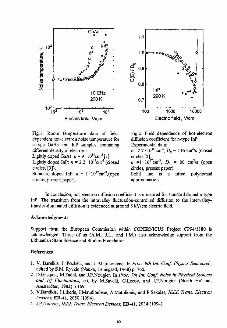
GaAs[] .
10GHz290 K
102 "'----'-.......................L.UJ.._-'---'.....................u.I.-----l
102 103 104
Electric field, V/cm
Fig.l. Room temperature data of fielddependent hot-electron noise temperature forn-type GaAs and loP samples containingdifferent density of electrons.Lightly doped GaAs: n = 9 . 10I4cm-3 [3].Lightly doped loP: n = 3.2 '1OIScm-3 (closedcircles, [3]);Standard doped loP: n = 1 '1017cm-3,(opencircles, present paper).
1.1
1.0
00 0.9--w.......0
0.8InP ......290K •
0.7 •
100 1000 10000
Electric field I V/crn
Fig.2. Field dependence of hot-electrondiffusion coefficient for n-type loP.Experimental data:n =2.7 '1015 cm-3, Do = 116 cm2/s (closedcircles [2],n =1 '1017cm-3, Do = 80 cm2/s (opencircles, present paper).Solid line is a fitted polynomialapproximation.
In conclusion, hot-electron diffusion coefficient is measured for standard doped n-typeloP. The transition from the intravalley fluctuation-controlled diffusion to the intervalleytransfer-dominated diffusion is evidenced at around 8 kV/cm electric field.
Acknowledgments
Support form the European Commission within COPERNICUS Project CP9411180 isacknowledged. Three of us (A.M., 1.L., and LM.) also acknowledge support from theLithuanian State Science and Studies Foundation.
References
1. V. Bareikis, 1. Pozhela, and L Matulioniene. In Proc. 9th Int. Con! Physics Semicond.,edited by S.M. Ryvkin (Nauka, Leningrad, 1968) p. 760.
2. D.Gasquet, M.Fadel, and lP.Nougier. In Proc. 7th Int. Conf. Noise in Physical Systemsand 11j Fluctuations, ed. by M.Savelli, G.Lecoy, and 1.P.Nougier (North Holland,Amsterdam, 1983) p.169.
3. V.Bareikis, 1.Liberis, LMatulioniene, A.Matulionis, and P.Sakalas, IEEE Trans. ElectronDevices, ED-41, 2050 (1994).
4. 1.P.Nougier, IEEE Trans. Electron Devices, ED-41, 2034 (1994).
62
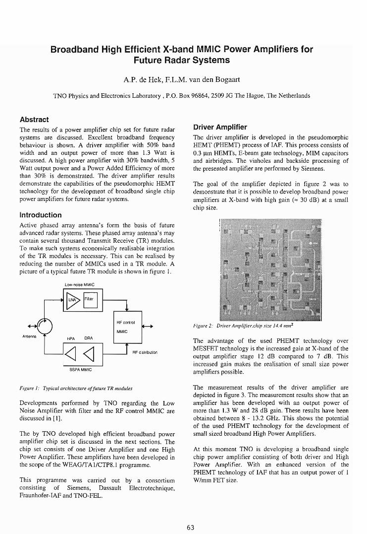
Broadband High Efficient X-band MMIC Power Amplifiers forFuture Radar Systems
A.P. de Hek, EL.M. van den Bogaart
TNO Physics and Electronics Laboratory, P.O. Box 96864, 2509 JG The Hague, The Netherlands
AbstractThe results of a power amplifier chip set for future radarsystems are discussed. Excellent broadband frequencybehaviour is shown. A driver amplifier with 50% bandwidth and an output power of more than 1.3 Watt isdiscussed. A high power amplifier with 30% bandwidth, 5Watt output power and a Power Added Efficiency of morethan 30% is demonstrated. The driver amplifier resultsdemonstrate the capabilities of the pseudomorphic HEMTtechnology for the development of broadband single chippower amplifiers for future radar systems.
IntroductionActive phased array antenna's form the basis of futureadvanced radar systems. These phased array antenna's maycontain several thousand Transmit Receive (TR) modules.To make such systems economically realisable integrationof the TR modules is necessary. This can be realised byreducing the number of MMICs used in a TR module. Apicture of a typical future TR module is shown in figure I.
Low·noise MMIC
RF control
MMIC
Driver AmplifierThe driver amplifier is developed in the pseudomorphicHEMT (PHEMT) process of IAF. This process consists of0.3 ~m HEMTs, E-beam gate technology, MIM capacitorsand airbridges. The viaholes and backside processing ofthe presented amplifier are performed by Siemens.
The goal of the amplifier depicted in figure 2 was todemonstrate that it is possible to develop broadband poweramplifiers at X-band with high gain ('" 30 dB) at a smallchip size.
Figure 2: Driver Amplijier.chip size 14.4 mm2
Antenna HPA ORA
<J<JSSPAMMIC
RF dislribution
The advantage of the used PHEMT technology overMESFET technology is the increased gain at X-band of theoutput amplifier stage 12 dB compared to 7 dB. Thisincreased gain makes the realisation of small size poweramplifiers possible.
Figure I: Typical architecture oJfuture TR modules
Developments performed by TNO regarding the LowNoise Amplifier with filter and the RF control MMIC arediscussed in [1].
The by TNO developed high efficient broadband poweramplifier chip set is discussed in the next sections. Thechip set consists of one Driver Amplifier and one HighPower Amplifier. These amplifiers have been developed inthe scope of the WEAGfTA I/CTP8.1 programme.
This programme was carried out by a consortiumconsisting of Siemens, Dassault Electrotechnique,Fraunhofer-IAF and TNO-FEL.
The measurement results of the driver amplifier aredepicted in figure 3. The measurement results show that anamplifier has been developed with an output power ofmore than 1.3 Wand 28 dB gain. These results have beenobtained between 8 - 13.2 GHz. This shows the potentialof the used PHEMT technology for the development ofsmall sized broadband High Power Amplifiers.
At this moment TNO is developing a broadband singlechip power amplifier consisting of both driver and HighPower Amplifier. With an enhanced version of thePHEMT technology of IAF that has an output power of 1W/mm FET size.
63

coefficients up to I.
"
_1-)
Figure 3: CW measurement result Driver Amplifier (Ps=3 dBm)
"..-r ---~ r-..../ ~
15
10
so
3S"
o1211• 10
FNqUency (GHz)
Output po..r~ PAE ot!he ""01- chip SW MESFET -mpitflM(VddV, cl... AlB. Input poWlK =25 dam)
,.// /' -.....:::::-
// L--,·<,,-r---....'-- ::-....
( / ~
/1 "-",,-II "'\. "-...-Poul(CW)
II 1-......'....... 1 ~-PAf(CWl
W-PAC(PuIMd)
Io7
35
3D
"
121110o
7
10
25
"
High Power AmplifierA 5-Watt High Power Amplifier is developed in theSiemens DIOM20HP process (Refs [I] and [2]). Thisprocess consists of 0.5 l!m MESFETs, a self aligned gatetechnology, localised ion implementation, MIM capacitors,via holes and airbridges. This technology offers highperformance, high reliability and good reproducibility atlow costs.
A photograph of the realised High Power Amplifier isshown in figure 4. The measured large-signal measurementresults are depicted in figure 5.
Figure 5: Measurement results 5-Wall Hi/ih Power Amplifier
Multiple-order input, interstage and output matchingnetworks are used in order to obtain the requiredbandwidth. Careful attention is paid to make the amplifiersstable. Stability analysis is carried out for all odd and evenmodes using open-loop transfer function techniques.Amplifier design is carried out with HP-EEsof softwareusing the EEFET3 transistor models. Parameter extractionfor this model is optimised to obtain a good agreementover the required bandwidth between model predictionsand measured transistor performance under high powerconditions and under optimum load conditions. Parameterextraction is carried out on transistors with exactly thesame size as those used in the high power amplifier. Atypical exemple is shown in fugure 6.
12x125xO.5 FET at Vds=9 V and V9s~1.6 V andop-.!im~~ad (0.61142.7° @f=10GHz)
'0
Fi/illre 6: Al:reemellt betweell modelled and mel/sured PAE of thetrallsis/tJr shown Oil the right side.
Fil:lIre 4: 5-Wall Hil:h Power Amplijier, chip size 22 mm2
The measurement results show that an excellentperformance has been obtained. The pulsed output poweris more than 5-Watt over a 30% bandwidth. The PowerAdded Efficiency is more than 30% over a 30%bandwidth. At 8.8 GHz a peak output power of7-Watt anda Power Added Efficiency of 40% has been measured.
MESFETs with a reduced drain-source spacing, but wellwithin the maximum tolerable temperature limits, are usedto reduce amplifier size. The output matching of thetransistors is based on measured 10ad-pull data. The loadpull data is obtained with an in-house developed uniquehigh-power on-wafer active load-pull system that iscapable of providing load impedances with reflection
ConclusionsThe driver amplifier developed in the PHEMT process ofIAF has a frequency bandwidth of more than 50%, anoutput power of more than 1.3 Watt and a gain of morethan 28 dB. The in the Siemens DIOM20HP processdeveloped High Power Amplifier shows and excellentoutput power of more than 5-Watt over a frequency bandof 30% at X-band. The power Added efficiency is morethan 30% over this frequency band.
ReferencesI. F.L.M. van de Bogaart, "Application Specific MMICstilr Advanced
Active Phl/sed-Array Antellnl/ 's", Cost 245 Proceedings, pp. 289 294, June 1996.
2. EL.M. van de Bogaart, A.P. de Hek, A. De Boer,"MESFEJ Hi/ihPower High-Ejjiciency Amplijiers l/t X-bl/lld with 30% bl/lldwidth",GAAS96 Symposium proceedings. June [996.
64

On the Design and Application of Narrow Tuneable MMIC Filters
F.E. van Vliet l, J.L. Tauritz2 and F.L.M. van den Bogaart1
1: TNO Physics and Electronics LaboratoryP.O. Box 96864, 2509 JG, The Hague, The Netherlands
2: Delft University of Technology, Faculty of Electrical EngineeringP.O. Box 5031, 2600 GA, Delft, The Netherlands
IntroductionSystem designers world-wide require miniature microwave filters. The potential market for these filtersis enormous. For narrow tuneable microwave filters, no off-the-shelf solutions are available. Specificareas where these filters are needed are high-performance front-ends such as used in e.g. satellitecommunication systems, radar systems and measurement equipment.Over the last five years, we have investigated monolithic GaAs filter integration. One of the results ofthese research efforts has been a design strategy to integrate narrow band pass filters. This strategy willbe discussed as well as recent results.
Design strategyThe main reason for the introduction of active elements in monolithic filters is the lack of high-qualitypassi ve components in standard GaAs technology. This limit results in filters that have at best amoderate bandwidth. Results of our research efforts were obtained using active inductors. The activeinductors are separately optimised to provide an optimal large-signal performance. They are used toform a tapped active resonator, where the tap is used to obtain a low impedance. The resonator is thenused to form a band stop filter. Band stop filters have been individually characterised, measured resultswill be shown. The band stop filter is in turn used in a differential structure, together with a matchedbro:ldband amplifier to result in the desirable band pass response. Measured results for these filters willbe shown. The bandwidth was measured to be as low as approximately 70 MHz, the noise figure 6 dBand the tuning range from 9 to 11 GHz.The filters were realised in Philips' d02ah process, using 0.2 11m PHEMTs that offer anfr of 62 GHz.
Non-ideal effectsThe resulting filters have a limited dynamic range. For the band pass filters described, however, thelarge-signal behaviour is highly frequency dependent. In the pass band, the sensitivity for large signalsis high. Large signals result in an increasing insertion loss. For the signals outside the pass band, wherethe large signals to be suppressed are expected, this sensitivity is significantly lower. Since large signalsmust be suppressed when outside the pass band, the situation may be well tolerable.
ConclusionAlthough the use of narrow MMIC filters in high-performance front-end requires a careful trade-off, webelieve that the introduction of MMIC filters adds significant advantages to the performance of thefront-end. The filters are the only available option, whenever small, fast-tuneable filters are needed.
References[I] F.E. van Vliet et. aI., Systematic analysis, synthesis and realization of monolithic microwave activeinductors, MTT-S 1996 Symposium Digest.[2] C. Rauscher. Microwave channelized active filters - a new modular approach to achievingcompactness and high selectivity. IEEE Transactions on Microwave Theory and Techniques, MTT44(1):122-132, January 1996.[3] D.K. Adams et. aI., "Active filters for UHF and microwave frequencies" IEEE Transactions onMicrowave Theory and Techniques, MTT-17(9):pp. 662-670, September 1969
65

Area Application Advantages
Civil Communication portable telephones small, light, potentially inexpensive
communication satellites small, light, remotely tuneable
Instrumentation generators less expensive
receivers less expensive
military Radar broadband phased-arrays small, low-cost, high tuning speed
Electronic Warfare frequency hopping high tuning speed
Figure 1: Table summarizing the main applications of narrow MMIC tuneable filters.
oFigure 2: Schematic of the band stop filter.
band stop filter ()V> 0""£ 3
cr
~ :;'all pass filter ~
Figure 3: Topology of the band pass filter.
Figure 4: Layout of the tuneable band pass filter.
66

Workshop on Compound Semiconductor Devices and Integrated Circuits (WOCSDICE)Scheveningen, The Netherlands, May 25~28, 1997
NOISE ANALYSIS OF InGaAs MIXER DIODES AT MILLIMETERWAVE AND FAR-INFRARED FREQUENCIES l
Phil Marsh and Dimitris PavlidisDepartment ofElectrical Engineering and Computer Science, The University ofMichigan,
Ann Arbor, MI 48109-2122, USA
InGaAs Schottky mixer diodes permit operation with reduced local oscillator power (FLO)compared with GaAs diodes and combine high sensitivity with integration capability with otherInP-based components. Diode design should lead to both conversion loss (Lc) and noisetemperature (Tmix) minimization. There are, however, several trade-offs that need to be made insuch optimization. For example high highly doped or thin n-InGaAs layers permit conversion lossreduction but may introduce tunneling currents and thus noise. The use of InGaAs instead ofGaAs allows larger r -L valley separation and thus reduced mixer losses due to electron scatteringand intervalley transfer. Moreover, the diode behavior needs to be analyzed under realistic nonequilibrium dynamic conditions as occurring in practice. It is the purpose of this paper to presentLc and Tmix extraction as obtained by Monte-Carlo simulation for various designs and comparesuch data with experimental results
The InGaAs diodes considered in this work were similar to the ones previously reported by theauthors and consisted of a low doped (-2x1017cm-3) n- region with thickness in the range of500A to 2000A and having a 1.4~m anode diameter. The DC bias diode noise (SOClOGHz)wasmeasured at IOGHz and the simulated noise was obtained from the short-circuit noise and currentcharacteristics obtained from Monte-Carlo analysis. Good agreement in nose characteristics isobtained between measured and simulated characteristics at low bias current IoC. However, asIoC increases, the measured noise increases more rapidly while their dynamic resistance remainsrelatively low (-170hm). Furthermore the measured noise showed an inverse relation withfrequency which was more pronounced at higher IoC; the noise temperature (Toe) declined byabout an order of magnitude as the frequency increased from 1.4GHz to lOGHz. These resultsindicate that InGaAs mixer diodes biased beyond their Schottky barrier height exhibit noise that isdominated by a mechanism which is not due to effects taken into account in our Monte-Carlomodel such as hot electron effects, impact ionization and intervalley transfer.
InGaAs and GaAs diodes of the above doping and 500A n- layer thickness were simulated asmixers as a functions of frequency and PLO and their Tmix and Lc showed the expected increaseswith frequency. The results demonstrate the superior performance of InGaAs vs. GaAs diodes interms of noise. The increase of noise with frequency is related to the increased importance ofscattering as the frequency increases while the improved performance of InGaAs mixer diodes isrelated to the InGaAs material's lower scattering rates and effective mass. At 1.2THz, similarInGaAs and GaAs diodes present minimum, double-sideband (DSB) Tmix'S of 385K and 430Krespectively, with respective associated single-sideband (SSB) Lc's of S.7dB and 6.4dB. A much
I This work was sponsored by ARO-URI Contract No. OAAL03-92-G-0109
67

higher advantage is expected at 4.8THz where the respective minimum InGaAs and GaAs DSBTmix'S are 1213K and 2106K with associated respective SSB Lc's of 10dB and IldB.
Overall, we present the noise and conversion Joss characteristics of high performance InGaAsdiodes for millimeter-wave and far-infrared frequency operation, analyze their noise properties bymeans of Monte-Carlo simulation which allows consideration of non-equilibrium effects andcompare their performance to the more traditional mixer technology based on GaAs.
InGaAs100Hz
(Measured)
I/
I
'N 7 ~-------"',""""----'"
~6
6 5....~4Q
~3...c::~ 2::sUII) 1en'0Z 0;!:.----5-.....1O..,......--1..".5~2~O,..-~25:---:!30~~3S
DC Anode Current (rnA)
Fig. IB: Noise current squared, vs. DC biascurrent. Here the n- layer thickncss and doping
are 2000A and 2xI017cm-3 respectively.
Measured InGaAs
104..__-------------,A
102L-__o....-__o....- ---J
o 5 10 15 20DC Anode Current (rnA)
Fig. lA: Noise temllerature, Tnc, vs. DC biascurrent. Here the n- layer thickness and dOlling
are 2000A and 2xlOI7cm-3 respectively.
0.1 0.5 1Local Oscillator Power (mW)
Fig. 2A: Simulatcd singlc-sideband mixerconversion loss as a function of local oscillatorIlower and frequency for InGaAs and GaAsdiodes having anode diameters of O.Sllm andO.8Ilm. Here the n- layer thickness and dopingare 500A and 2x1017cm-3 respecth'ely. The NSsuffix means these diodes were simulatcd with allelectron scattering mechanisms disablcd.
105------------g B~
~ 104~
8E~ ,4.&m.......l~~2S~~~~ 10
3',''0 ~. *"o:::=.OaAs_.&J.l.
Z '~---'---~ 1.2mz - - ~aAs_.8J.l.mo 1021.- -.1
0.1 0.5 1 5 10Local Oscillator Power (roW)
Fig. 2B: Simulated double-sideband mixer noisetcmpcrature as a function of local oscillator powerand frequency for InGaAs and GaAs diodeshaving anode diameters of O.SJ.1m and O.8Ilm.Hcre the n- 1l1)'Cr thickncss and doping al'e 500A
and 2x1017cm-3 resllectively. Thc NS suffix meansthese diodcs wel'c simulated with all electronscattering mechanisms disabled.
68
Monday, May 26
16.00 - 18.00 Session 4: Quantum Effects and Tunneling
16.00 1. (Invited Paper) K. Von Klitzing, Max Planck Institute Stuttgart:"Semiconductor quantum devices"
16.302. (Invited Paper) M. Yamamoto, NIT System Electronics Labs.:"Resonant Tunneling Diode and HEMT Integrated Devices andCircuits".
17.003. A. Sigurdardottir, K. Mutamba, A. Vogt and H.L. Hartnagel:"Investigation on Tunnelling Effect in Stressed InAs/AISb/GaSbResonant Tunnelling Diodes".
4. M.I. Lepsa, Th.G. Van de Roer, J.J.M. Kwaspen, W Van der Vleuten,L.M.F. Kaufmann:
"Three Terminal Double Barrier Resonant Tunneling DevicesBased on the Direct Contacting of the Quantum Well".
5. Jozsef Karanyi and Bela Szentpali:"Quantum mechanical tunneling in GaAs ohmic contacts".
6. J.J. M. Kwaspen, M.I. Lepsa, Th.G. Van de Roer, W Van der Vleuten,H.C. Heyker, L.M.F. Kaufmann:
"Accurate Equivalent-Network Modeling of GaAs/AIAs BasedResonant Tunneling Diodes with Symmetrical Thin Barrier andSpacer Layers"
69

Semiconductor Quantum Devices
K. Von KlitzingMax Planck Institut fuer Festkoerperphysik
Heisenbergstrasse 1D-70569 Stuttgart
Germany
Epitaxial growth is an established method for the production of a large number of
semiconductor devices where the thickness of the active layer has to be controlled
with high accuracy. Quantum wells, resonant tunnel diodes, superlattices or the
cascade laser are typical examples. Whereas the control of layer thicknesses in the
growth direction for the realization of two-dimensional electron systems is relatively
simple, optical and electron beam lithography are normally necessary to produce a
lateral confinement of the electronic system in the range 0.05 - 0.5 ~lm (one- and
zero-dimensional electron systems). However the Stranski-Krastanov growth and
the MBE-growth on patterned substrates opened new ways for the realization of one
and zero-dimensional electron system. Recent optical and transport measurements
on self-assembling InP and GaAs quantum dots are presented with the focus on
single electron devices.
70

Resonant Tunneling Diode and HEMT Integrated Devices and Circuits
Masafumi Yamamoto
NTT System Electronics Laboratories3-1 Morinosato Wakamiya, Atsugi-shi, Kanagawa 243-01, Japan
This paper reports our recent activities aiming at constructing quantum functional devices andcircuits based on the monolithic integration of InP-based resonant tunneling diodes (RTDs) and highelectron mobility transistors (HEMTs).
We demonstrate an approach of employing series-connected resonant tunneling (RT) deviceswith a peak current modulation scheme driven by an oscillating bias voltage. This approach makepossible the implementation of a variety of quantum functional circuits with reduced complexity.The principle of operation is to control the switching sequence of these RT devices at the rising edgeof the oscillating bias voltage by changing the effective peak currents, using control gates. Weemployed a newly developed InP-based RTD and HEMT parallel-connected integrated device. Inthis device, the effective peak currents can be modulated through the gate voltage applied to theHEMT.
We also report that an InP-based resonant tunneling high electron mobility transistor (RTHEMT)features a pronounced negative differential resistance (NDR) and a negative transconductance, andis suitable for high-performance RF device applications.
With the use of an RTD as a quantum effect device in combination with a HEMT, these InP-basedRTDIHEMT integrated devices and circuits can fully utilize the functionality arising from NDR atroom temperature.
I. Introduction
The negative differential resistance (NDR) of resonant tunneling (RT) devices offer the possibilityof greatly reducing circuit complexity [1-5]. A resonant tunneling diode (RTD) provides clear NDR atroom temperature. It also provides high peak current density, resulting in ultrahigh-speed switchingtimes that reach 1.5 ps for InP-based RTDs [6].
To create viable quantum functional devices and circuits, the development of circuit configurationthat can fully utilize NDR characteristics is indispensable. The development of a three-terminal RTdevice suitable for integration is also a key issue.
A monostable-to-bistable transition logic element (MOBILE) consists of two series-connected RTdevices with a peak current modulation scheme and is driven by an oscillating bias voltage [4]. AMOBILE provides multi-input and multi-output capabilities without sacrificing the intrinsic high-speedcharacteristics of RTDs. It also features weighted sum threshold logic with both positive andnegative weights [7].
These advantages make MOBILEs suitable for applications in parallel processing architecturesfor computation such as artificial neural networks or cellular automata [4]. Indeed, simple onedimensional cellular automata for a random sequence generator have been demonstrated [8].
We recently demonstrated that a variety of functional circuits of reduced complexity can beconstructed by extending the circuit concept of the MOBILE to include three or more RT devicesconnected in series. The principle of operation behind a generalized circuit is to control the switchingsequence of these RT devices at the rising edge of the oscillating bias voltage by changing theeffective peak currents, using control gates. The basic RT device we employed was a newly developed
71

InP-based RTD and high electron mobility transistor (HEMT) parallel-connected integrated device inwhich the effective peak currents could be modulated through the gate voltage applied to the HEMT.
Based on this circuit concept, we designed a literal gate (one of the fundamental multiple-valuedlogic gates), an analog-to-quaternary quantizer, and a programmable logic gate performing AND,OR, NAND, NOR and XOR according to the appropriately applied control voltages. We fabricatedthese, using the InP-based RTDIHEMT monolithic integration technology. We then experimentallyconfirmed the proper operation of these functional circuits at room temperature.
The InP-based resonant tunneling high electron mobility transistor (RTHEMT) incorporated apseudomorphic InGaAs/AlAslInAs RTD into the source of a non-alloyed ohmic contact lnAlAslInGaAsHEMT. We demonstrated that this device features a pronounced NDR and a negative transconductancealso at room temperature.
ll. InP-Based Resonant Tunneling Diode and HEMT Integrated Device in ParallelConnection
Development of a basic NDR device with a peak current modulation capability suitable forintegration is essential in furthering the applicability of quantum functional circuits based on MOBILEs.We recently developed an InP-based RTD and HEMT parallel-connected integrated device [9]. Itsepitaxial layer structure is shown in Fig. 1. The effective peak current can be modulated through thegate voltage applied to the HEMT, as shown in Fig. 2. This approach enables the separate optimizationof an RTD showing NDR characteristics and a HEMT responsible for peak current modulation. Thisseparate optimization is advantageous for reproducibility and uniformity, which are indispensablefor integration.
On the same wafer, we obtained a high peak current density of 9 x 10⁴ Ncm 2 with a goodpeak-to-valley ratio of 5.5 for InGaAs/AlAslInAs RTDs and a maximum transconductance of 850mS/mm for 0.7 Ilm-gate-Iength lnAlAslInGaAs HEMTs at room temperature.
Another advantage of this technology is that it enhances circuit design flexibility by usingRTDIHEMT integrated devices with a combination of HEMTs in peripheral circuits on the samewafer.
llI. Quantum Functional Circuits Based on Series-Connected Resonant Tunneling Deviceswith Peak Current Modulation Capability
To further the applicability of MOBILEs, it is also essential to develop a variety of quantumfunctional devices and circuits. For this purpose, we recently proposed a monostable-multistabletransition logic gate (MML). This is based on a generalization of the device concept of the MOBILE,by increasing the number of series-connected RT devices up to three or more [101. The principle ofoperation is to control the switching sequence of these RT devices during the critical period ofincreasing the oscillating bias voltage by changing the effective peak currents, using control gates,before this critical period.
Figure 3(a) shows a circuit configuration of a literal gate composed by the MML device concept[101. A literal gate is one of the basic logic gates in multiple-valued logic (MVL). The present literalgate is composed of the three NDR devices A, B and X connected in series and driven by anoscillating bias VCK' The effective peak currents ofNDR devices B and X are modulated through thegate voltages applied to HEMT1 and HEMT2 connected in parallel with the RTDs B and X, respectively.The maximum value of VCK is selected so that one of the three NDR devices is switched from thepeak to valley state. The device switched at the rising edge of VCK is the one having the smallesteffective peak current. By designing the transconductance of HEMTI and HEMT2 differently throughthe gate widths, we can control the relative magnitude of peak currents, as shown in Fig. 3(b).
72

Based on this principle, we can obtain the literal operation. Its Vout versus Yin characteristics areshown in Fig. 3(c). By using the InP-based RTDIHEMT integration technology, we successfullydemonstrated the literal operation at room temperature, as shown in Fig. 3(d).
The device concept of the present literal gate can be extended to implement a two-input logicgate. Furthermore, by introducing two control voltages, a programmable logic gate can be constructed[11]. Its circuit configuration is shown in Fig. 4(a). By varying the control voltages Vconi and Vcon2 '
one of the five logic functions of AND, OR, NAND, NOR and XOR can be selected. By varying themaximum value of the oscillating bias voltage, the logic function ofXNOR can also be obtained. Theprogrammable logic functions were confirmed experimentally, and the EXOR operation is shown inFig.4(b). This flexible logic gate is promising for the implementation of programmable logic circuits.
The literal gate and programmable logic gate described above include one NDR device betweenthe output terminal and ground, resulting in an output level of "I" or "0". By increasing the NDRdevice number up to two or more between the output terminal and ground, MVL circuits havingmultiple-valued output can be constructed.
Figure 5(a) shows the circuit configuration of an analog-to-quaternary quantizer consisting of sixNDR devices connected in series, where three NDR devices X, Y, and Z are involved between theoutput terminal and ground [12]. The maximum value of the oscillating bias voltage VCK is chosen sothat the three NDR devices out of the six are switched. By varying the relative magnitude of theeffective peak currents of NDR devices through the input signal applied to the HEMT as shown inFig. 5(b), the switching sequence can be controlled. This results in the Vout vs. Yin characteristicsshown in Fig. 5(c). Here, four different levels of output voltage were obtained as a function of Vin •
These resulted from the differing number of switched NDR devices involved between the outputterminal and ground at the rising edge ofVcK' Proper operation was also confirmed experimentally,as shown in Fig. 5(d).
The present analog-to-quaternary quantizer will be useful for implementation of multiple-valuedlogic circuits and analog-to-digital converters.
These quantum functional circuits are advantageous in reducing circuit complexity in terms oftotal number of devices and logic gates in the critical path. This in turn would result in low powerconsumption and high-speed operation.
IV. InP·Based Resonant Tunneling HEMT
In implementing high-performance analog RF devices, it is essential to utilize active deviceswith strong nonlinear characteristics. To achieve functional devices with such characteristics, werecently developed an InP-based resonant tunneling high electron mobility transistor (RTHEMT)[13].
An InP-based RTHEMT incorporates a pseudomorphic InGaAs/AlAsllnAs RTD into the source ofa non-alloyed ohmic contact InAIAsllnGaAs HEMT. Figure 6(a) shows an SEM photograph of afabricated RTHEMT. The epitaxial layer structure is the same for the RTD and HEMT parallelconnected integrated device, and only the wiring is altered to obtain the series connection of an RTDandaHEMT.
Figure 6(b) shows the source-drain I-V characteristics of an RTHEMT at room temperature. Apronounced NDR is clearly obtained. A most significant feature is that the drain current Ins saturatesnear the valley current after the resonance peak. The key mechanism of this near-flat valley currentis ascribed to the drastic change of the potential of the floating source (Vs') of the HEMT arising fromthe switching of the RTD from peak to valley that occurs when the Ins exceeds the RTD peak current.The result is the decreased effective gate voltage (VGS') and hence lowered saturation current of theHEMT. The effect is enhanced by the high transconductance and significantly reduced parasiticresistance of the present non-alloyed ohmic contact InAlAsIInGaAs HEMT.
73

Figure 6(c) shows the transfer characteristics at VDS =2 V; a pronounced negative transconductance(NT) is clearly shown. As a result of the near-flat valley current, the NT is obtained in a wide rangeofVDs ' This is attractive for circuit applications with a large operating margin.
The strong nonlinearity of the RTHEMTs presented here is highly preferable for use in highperformance analog devices, including frequency multipliers [14], mixers, oscillators, etc.
v. Summary
In summary, we have shown that a novel class of logic circuits, such as literal gates, programmablelogic gates, and analog-to-quaternary quantizers, featuring enhanced design flexibility along withreduced circuit complexity, could be constructed based on series-connected resonant tunneling deviceswith a peak current modulation scheme driven by an oscillating bias voltage.
We have developed an InP-based RTD and HEMT parallel-connected integrated device for useas a basic resonant tunneling device capable of peak current modulation. We have successfullyemployed this device to demonstrate the proposed quantum functional circuits at room temperature.
We have also demonstrated that the RTHEMT, having an InGaAs/AlAsllnAs RTD incorporatedinto the source of an lnAlAsllnGaAs HEMT, features a pronounced negative differential resistancewith a near flat valley current and a negative transconductance.
Clarification of useful targets for applications is a key issue for further advancement. In thiscontext, high-performance RF analog circuits constructed with RTHEMTs are highly attractive.The literal gate and analog-to-quaternary quantizer offer the potential to construct viable multiplevalued logic circuits. Furthermore, the analog-to-quaternary quantizer will be useful for theimplementation of high-speed analog-to-digital converters. The programmable logic gate is promisingfor the implementation of programmable logic circuits.
The RTD/HEMT integrated devices and circuits offer enhanced functionality and room temperatureoperation. We expect them to be useful in future electronic systems.
References
[1] F. Cappasso, S. Sen, and F. Beltram, in High-Speed Semiconductor Devices, ed. S. M. Sze,p. 465, John Wiley & Sons, New York, 1990.
[2] M. Takatsu, K. Imamura, H. Ohnishi, T. Mori, T. Adachihara, S. Muto, and N. Yokoyama,IEEE J. Solid-State Circuits, vol. 27, p. 1428, 1992.
[3] A. C. Seabaugh, A. H. Taddiken, E. A. Beam III, J. N. Randoll, Y. -C. Kao, and B. Newell,Tech. Dig. IEDM'93, p.419, 1993.
[4] K. Maezawa, T. Akeyoshi, and T. Mizutani, IEEE Trans. Electron Devices, vol. 41, p.148, 1994.[5] H. Goronkin, S. Tehrani, J. Shen, G. Kramer, and R. K. Tsui, Tech. Digest, GaAs Ie Symp.
1994, p.9.[6] N. Shimizu, T. Nagatsuma, T. Waho, M. Shinagawa, M. Yaita, and M. Yamamoto, lEE
Electronics Lett., vol. 31, p. 1695, 1995.[7] T. Akeyoshi, K. Maezawa, and T. Mizutani, Jpn. J. Appl. Phys., vol. 33, p. 794, 1994.[8] K. Maezawa, T. Akeyoshi, and T. Mizutani, IEEE Trans. Electron Devices, vol. 42, p.l005, 1995.[9] K. J. Chen, K. Maezawa, and M. Yamamoto, IEEE Electron Device Lett., vol. 17, p. 127, 1996.
[10] T. Waho, K. J. Chen, and M. Yamamoto, IEEE Electron Device Lett., vol. 17, p. 223, 1996.[11] K. J. Chen, T. Waho, and M. Yamamoto, IEEE Electron Device Lett., vol. 17, p. 309, 1996.[12] T. Waho, K. J. Chen, M. Yamamoto, to be published in Jpn. J. Appl. Phys.[13] K. J. Chen, K. Maezawa, and M. Yamamoto, Appl. Phys. Lett., vol. 67, p. 3608,1995.[14] K. J. Chen and M. Yamamoto, IEEE Electron Device Lett., vol. 17, p. 235, 1996.
74

Drain
InGaAs. 100 nm1x1018 cm-3
i-lnAIAs: 20 nm ]
~§§~~~~~~~~§§~~ schottky barrieri-lnGaAs channel, 15 nm n+-lnAIAs:, 4 nm
f---;";i-;';';'n;;;';AI;;"As::;'b';;;u~ffe:;';;r':':,2o:.00":'::":nm';;';';"---1 \ carrier supply layer
S I I P S i-lnAIAs, 2 nm HEMT.. n ubstratespacer
Fig. 1. Schematic cross section ofthe InP-based integrateddevice, in which an RTD and HEMT are connected inparallel.
'4
o 0.5 1 1.5
VDS
(V)
Fig. 2. I-V characteristics of anintegrated device, in which one RTDis in parallel with three HEMT's witha nominal 1: 2: 4 (2.5 : 5 : 10 11m) gatewidth ratio. The modulationamplitude of the total current isproportional to the gate width. Thecurves for gates 2 and 3 are shiftedfrom the origin for clarity.
Peak current(a) (b) (d)
A -IVVCK-OV
V,"~B B
-0.5VVVOUT II In lD
-OV(c)
X VOUl VOHIGH -0.5V
X:On X: Off X:OnV
OUl -OV
VOLOW
Yin
Fig. 3. Literal gate. (a) Circuit configuration. (b) Effective peak currents of A, B, and X as afunction ofV . (c) V vs. V characteristics showing literal operation. (d) Literal operation obtained
tn out m
for a fabricated circuit at room temperature.
A
(b)
A
B
Vout
OV
HEMT2 HEMT4 HEMT6B
Fig. 4. Programmable logic gate. (a) Circuit configuration. (b) Experimental demonstrationof the XOR operation.
75

Peak current (b) (d)
(a)VCK
VCK
Load Vin
VOUT
HEMT
V1No--1 VOU' (c) V..,
Fig. 5. Analog-to-quaternary quantizer implemented with six NDR devices connected in series.(a) Circuit configuration. (b) Effective peak currents of six NDR devices as a function ofVin •
(c) Vou' vs. Vin characteristics. (d) Circuit operation of a fabricated analog-to-quaternary quantizer.
(a)
~ate I
Drain
S'
Source
......300 CP
g200 ~
::J
"100 6uII)c
~0L............=:w.............~~~ ...............~....J-0.5
(c)
200 ,...................~""'T"'~~~T"'"""'"~ ............., 500 ee
400 iiie
til
~ 50
'E 150
e~ 100
20.5 1 1.5Vos (V)
oo
(b)
5
4 Vos=O.6 V T=300K
0(O.SV
E 3 O.3V-til_0 2
1
Fig. 6. Resonant tunneling HEMT. (a) SEM photograph of a fabricated RTHEMT. TheRTD has an area of 2 x 311m2. The gate length is 0.7 11m and width is 20 11m. The insetshows the equivalent circuit. (b) The source-drain I-V characteristics at room temperature.(c) The transfer characteristics at Vol> =2 V.
76

Investigation on Tunnelling Effect in Stressed
InAs/AISb/GaSb-Resonant Tunnelling Diodes
A. Sigurdardottir, K. Mutamba, A. Vogt, H.L. Hartnagel
Institut fur Hochfrequenztechnik, Technische Hochschule Darmstadt
Merckstr. 25, 64283 Darmstadt, Germany
Tel.: +49 6151 162162, Fax: +49 6151 164367
email: [email protected]
In the last years resonant tunnelling diodes (RTDs) have been of increasing
interest for different applications. Several studies including both fabrication and
characterization of RTDs have been carried out in order to increace for example the
peak to valley current ratio and the peak current. For high frequency applications
the device capacitance is of an extremely high importance. Some capacitance models
for AlAs/GaAs- and GaAs/GaAlAs RTDs have already been introduced in [1], [2]
and [3]. An interesting application of a double barrier RTD (DBRTD) as a pressure
sensor has been presented in [4] and [5].
For an improved understanding of the tunnelling effect and the capacitance
in DBRTDs we measured the current voltage characteristics and the capacitance
voltage characteristics of InAs/AISb/GaSb-resonant interband tunnelling diodes
(RITD) as a function of uniaxial pressure. The RITDs show a special pressure
dependence of the current voltage characteristics, which is due to the particular
tunnelling path involved in the conduction mechanism.
The RTDs considered here have been grown by MBE on a (OOl)-oriented GaAs
substrate. They consist of two undoped AISb barriers of width 25 A and an undoped
65 AGaSb quantum well. There are 10 nm thick undoped InAs spacer layers on both
sides of the double barrier structure. The double barrier structure is sandwiched
between two 1 x 1017cm-3 n-doped InAs injection layers of 50 nm width. The
electrodes consist of heavily doped (1 x 1018cm-3 ) InAs layers. Non-alloyed Cr/Au
ohmic contacts have been used.
77

References
[1] T. Wei, S. Stapleton: Solid-State Electronics, Vol. 38, No.2, pp. 465-469 (1995)
[2] T. Wei, S. Stapleton, O. Berolo: J.Appl.Phys. 8, 4071 (1995)
[3J T.G. van de Roer, H.C. Heyker, M. Kwaspen, M. Lepsa, W. van del' Vleuten,
M. Henini: 19th \Vorkshop on Compound Semiconductor Devices and Inte
grated Circuits, (KistajStockholm, May 21-24, 1995)
[4J K. Mutamba, A. Vogt, A. Sigurdarclottir, J. :Miao, A. Dehe, 1. Aller, H.L. Hart
nagel: Uniaxial stress dependence of AlGaAsjGaAs RTD characteristics for
sensor applications, Proc. Micromechanics Europe MME'96, p. 85 (Barcelona,
1996)
[5J K. Mutamba, M. Flath, A. Sigurclarclottir, A. Vogt, H.L. Hartnagel: Lithuanian
J. Phys. 36, No.6, 563-565 (1996)
78

THREE TERMINAL DOUBLE BARRIER RESONANT TUNNELING DEVICES BASED ONTHE DIRECf CONTACfING OF THE QUANTUM WELL
M. I. Lepsa·, Th. van de Roer, J. 1. M. Kwaspen,W. van der Vleuten, and L. M. F. Kaufinann
COBRA Institute, Eindhoven University of Technology,Eindhoven, The Netherlands.
Abstract
Three tenninal (31) Double BarrierResonant Tunneling (DBR1) devices with the base contact to the quantum well have beenfabricated from GaAslAlAs material system. The plane of the very thin quantum well is reached using high selective etchingprocesses and a nonalloyed Ti/PtIAu metallization scheme is used to obtain a Schottky base contact. DC and AC electricalmeasurements demonstrate that the base contact lies on the quantum well of the device DBRT structure and the base voltagemodulates the collectorcurrent It is shown that the electrical characteristics of these devices enlarge the possibilities of investigationof the DBRT structures and suggest important applications in high-speed electronics.
Introduction
From the beginning the long range application of the resonant tunneling structures was their implementation in three terminaldevices. A particularly powerful concept for achieving this has been to incorporate a double barrier resonant tunneling structure intoone or another of the junction or transport regions of a bipolar [1], hot electron [2], or field effect transistor [3]. In thisimplementation the primary operational parameters are those of the "traditional" device, with the tunneling features added to alterthese characteristics. However, in order to take advantage of the potential high speed and small size of the resonant tunnelingstructures it is obvious that the structure itselfhad to be processed for a 3T device. This approach consists in to make direct contactto the quantum well ofa DBRT structure and thereby form a 3T device in which the quantum well base is two-dimensional (2D),with transport proceeding from three dimensional (3D) emitter to 2D base and then to 3D collector. The primary challenge of thisapproach consists in the difficulty of exposing and making contact to a such thin layer (- 5nm) as the quantum well base. Thistechnological obstacle determined that similar tries for the obtaining of 3T-DBRT devices to conduct only to partial results [4, 5],the total settlement ofthe problem being under way. In this paper we propose a solution to fabricate such a 3T-DBRT device, basedon GaAs/AIAs material system. Our 3T-DBRT device originates from a "classical" DBRT structure so a transistor action is notobtained because there is no separation between the controlling and current-carrying electrons. Even then, it demonstrates interestingelectrical properties which permit for example the investigation of the switching characteristics of the DBRT structure and suggestsome applications.
Device Description and Fabrication
A schematic cross section ofthe 3T-DBRT device is shown in Fig. I. The GaAslA1As heterostructure was grown by molecularbeam epitaxy on a semi-insuIating GaAs substrate. The double barrier region, comprising 2.5 om barriers and a 5 om quantum well,was embedded by 2.5 nm GaAs spacer layers, all unintentionally doped. Surrounding these layers were grown low doped and contact(n++) GaAs layers. The device processing consisted mainly in mesa etching steps for the collector, base and emitter definition,followed by the corresponding contact deposition using the lift off technique. In all these processes opticallithography was used. The plane of the quantum well was reached by high selective dry etching using pure Freon~ 12 (CCI~;) inconventional planar RIE system while the other two mesa processes were carried out by wet chemical etching. The metallizationscheme consisted ofGelNilAu for the emitter and collector ohmic contacts and Ti/PtIAu for the quantum well base contact. Finally,specific contact pads suitable for microwave measurements using Cascade probes were deposited and air bridge interconnectionswere grown between these and the device contacts by gold electroplating.
Results
Both three tenninal and two terminal DC I-V characteristics of the 3T-DBRT devices were measured (see Figs. 2 and 3). TheI-V characteristics between Base-Emitter (B-E) and Base-Collector (B-C) terminals demonstrate that the base contact lies on thequantum ~ll ofthe device DBRT structure. During processing a thin oxide layer is interposed between the base (Schottky) contactand quantum well material. The DBRT structure which arises between the oxide layer and the second AlAs barrier of the basic
• Permanent address: National Research Institute for Material Physics, P.O. Box Mg-7 Magurele, 76900 Bucharest, Romania.
79

100 -- ••••• ----~•••••• ~-~--•••• --- ••••
- ~ .......
20
......... ···········1···········-10.
'". r---..---,---;----,.:..-
-":1 ••
ct=J ............---~ .....c=:J cw. ..,.."",---~ 0..._
Fig. 1 Schematic cross section of the 3T-DBRT device.The paths 1, 2, 3 and 4 indicate the possibilities of thecurrent flow.
Fig.2 Conunon emitter I-V characteristics of the 3T-DBRTdevice for different base constant currents.
25.0.----..,...---.,---..,..---,
20.0 -. -- -- ..---t-- --...--_..--.... i-1$.0 •• ---••• - •• +--- ---.- -.. *.--- .••-~. --*•.••-
1,0.0 ... --...---+.--..------ .--...-.... t--····-···--...,. ! i
5.0 ••••••••••••1"" ·r···········0.0
.... .-----,...--..-----;----;-----,
-.- _~.- -- - _--..~._-_...._-:.- --..
: ~ +...... l ..._..----t··..----. ..---- i--·
! :·-----···t---····~- -····---·1-· -
, '0&0 --•••-.--!....._-......---... -1 -••••••• -; •••••••••
: :
-5.~L.~~~•..l.2.~~........J••~~...J-2;,...0~~......J••
v.. [V]
(8)Fig.3 Two tenninal B-E (a) and B-C (b) I-V characteristics of the 3T-DBRT device.
v.. [V)(b)
structure accounts for the B-E characteristic. Further on, the B-C characteristic is the result of two DBRT structures connected inseries because the large depletion region underneath and laterally the base surface detennines the current to follow the path 4,showed in the cross-sectional picture ofthe 3TDBRT device. Further on, the conunon-emitter characteristics of the device presentedin Fig. 3 show clearly that the collector current is modulated by the quantum well base potential. They can be explained,qualitatively, making use of the physical picture (energy band diagram) of the DBRT structure. The device transfer characteristic(collector current function ofbase current) shows abrupt switching properties. Using microwave measurements, the conclusionsestablished in DC conditions have been confirmed. We have used the third device tenninal to measure the switching time of ourDBRT structure in a much more simple way than previously reported efforts [6, 7]. The experimental value for this parameter is inaccordance with the theoretical estimation using the DC properties ofthe device.
The electrical characteristics ofour 3T-DBRT devices suggest the possible use of these in fast switching applications and highfrequency tunned oscillators.
References
1. N. Yokoyama, K. Imamura, H. Ohnishi, T. Mori, S. Muto, and A. Shibatomi, Solid-State Electronics 31, 577 (1988).2. A C. Seabaugh, E. A Beam ill, A H. Taddiken, J. N.Randall, andY.-C. Kao, IEEE Electron Device Lett. 14,472 (1993).3. T. K. Woodward, T. C. McGill, and R. D. Burnham, Appl. Phys. Lett. 50,451 (1987).4. G. I. Haddad, R. K. Mains, U. K. Reddy, and 1. R. East, Superlatt. Microstruct. 5,437 (1989).5. M. A. Reed, W. R. Frensley, R. J. Matyi, 1. N. Randall, and A C. Seabaugh, Appl. Phys. Lett. 54, 1034 (1989).6. 1. F. Whitaker, G. A Mourou, T. C. L. G. SolIner, and W. D. Goodhue, Appl. Phys.Lett. 53,385 (1988).7. S. K. Diamond, E. Ozbay, M. J. W. Rodwell, D. M. Bloom, Y.C. Pao, E. Wolak, and J.Harris, Jr., in "OSA Proceedings
on Picosecond Electronics and Optoelectronics", Vol. 4, p. 101, Optical Society ofAmerica, Washington, D.C., 1989.
80

Quantum mechanical tunneling in GaAs ohmic contactsJ6zsef Karanyi and Sela Szentpali
Research Institute for Technical Physics ofHungarian Academy ofSciences,
Budapest
P.o.B 76, H-1325, Hungary.
E-mail:karanyi@mufi·[email protected]
The ohmic contacts on GaAs are generally supposed to be Schottky barriers with very
thin space charge layers due to the high dopant concentration. The current flowing through
them obeyes quantum mechanical tunneling [1] [2] [3]. It is obvious to assume that the doping
atoms occupy randomly the lattice sites and therefore the shape of the potential in the space
charge layer exhibits variations even in the case of uniform doping. The expected effect should
be greater when the space charge width is in the range of the average distance of the doping
atoms, Le. in the case of higher doping concentrations. Therefore refinements of the picture
take into account the potential variations in the space charge layer caused by the random
distribution of the dopants [4] [5] [6]. In the present work we investigate this fluctuations by
Monte-Carlo simulation. The results of the different theories and our computations are
reviewed and compared with the last published measurements [7].
The plane of the junction was assumed to be equipotential and this boundary
condition was introduced into the computations by the electrical image method. The
electrostatic potential was computed in a prismatic volume in which the positively charged
donors were randomly distributed in the points of a cubic lattice having a constant of
GaAs (0.56 run). The top surface of the prism is 0.5*0.5 I-lm2 which is a macroscopic area. The
space charge region is bounded by the equipotential surface belonging to V=O. The depletion
approximation was used Le. the charges of donors out of this boundary were not taken intoaccount. For removing the edge effect the central prismatic region in which the computations
were made was embedded in two successive regions: the first neighbouring one which has a
width of the double of the average of depletion layer and the second one which extends to the
infinity. The charges were distributed also randomly in the first region while in the second one
a continuous space charge equal to the average of the doping was considered. The values of
the electrostatic potential were computed in equidistant grid points in cross-sectional planes
parallel to the junction.
In the case of moderate doping concentrations the average potential follows well the
parabola known from the continuous space charge model, however the widths and forms of the
elementary potential functions differ significantly. For higher doping (over 1019cm0
3) even the
average potential does not fit to the continuous model. The currents were computed along
each elementary square according to the WKB approximation.Through the thinner depletion
regions quasi-exponentially more tunnelling currents flow.
81

The following table shows the doping concentrations according to the different
models (rows) fitted to the measured contact resistance values (columns):
experiment [7] NiGeAu/n-GaAs(2* 1018cm-3) PdGeTiPtln-GaAs(2* 1018cm-3
)
metalisation and heat 350°C /15s 390°C /90s 350°C /15s 390°C /90s
treatment
contact resistance (300K) 28.7 mWcm2 0.66 mWcm2 0.35 mWcm2 8.2 mWcm2
1 continuous model [4] 1.6*1018 2.5*1018 3.0*1018 1.8*1018
2 continuous model [3] 1.5*1018 3.0*1018 3.2*1018 1.8*1018
3 quasi-cont. model [2] 2.3*1018 3.3*1018 3.8*1018 2.4*1018
4 Monte-Carlo model [4] 1.4*1018 2.0*1018 2.3*1018 1.6*1018
5 Monte-Carlo model [5] 2.0*1018 3.0*1018 3.5*1018 2.2*1018
First column represents the case where the metal is not alloyed. The 1, 2 and 4 models
result a lower doping concentration than the original one. These models seem to overestimate
the tunneling current. The 3 and 5 models seem to be closer to reality. The second and third
columns represent the experimental situation where the doping concentrations have been
increased under the metalization by alloying or sintering. In these cases all models result in
higher concentrations. It is difficult to judge them because there are no independent data of
doping but it should be noted that the model 4 ~ives the original concentration only. The fourth
column shows the compensation effect due to the amphoteric behaviour of Ge [7]. Here the
models 1, 2 and 4 show again lower concentrations than the original one.
ACKNOWLEDGEMENT: This work have been supported by the Hungarian National
Scientific Research Found (aTKA) under grants TO 15612, TO 22487 and by the EC under
Copernicus 941180 contract.
IE. H. Rhoderick and R. H. Williams, Metal-Semiconductor Contacts (Clarendon 1988)
2C.y'Chang, Y.K.Fang, S.M.Sze, Solid-State Electron. 14, 541 (1971)3J.Crefton and P.A.Bames, 1. AppI. Phys. 69, 7660 (1991)
'W.1.Boudville and T.C.McGill, 1. Vac. Sci. TechnoI. B 3, 1192 (1985)
sJ.Karimyi and B.Szentpali, in Prec. CAS'94 11-16 Oct 1994, Sinaia, Romania, 81
6V.Freilikher et al., Phys Rev. B, 53, 7413 (1996)7K.A.Jones et aI., AppI. Phys. Lett., 69,4197 (1996)
82

ACCURATE EQUIVALENT-NETWORK MODELING OF GaAslAIAs BASED RESONANTTUNNELING DIODES WITH SYMMETRICAL THIN BARRIER AND SPACER LAYERS
*JJ.M. Kwaspen, M.1. Lepsa , T.G. van de Roer, W. van der Vleuten,H.C. Heyker, L.M.F. Kaufmann
COBRA Institute, Eindhoven University of Technology, Eindhoven, The Netherlands
Abstract
Both the classical Esaki and the Quantum-Inductance equivalent-network models [1,2,3] are usedin this work to describe the bias-voltage and microwave frequency dependency of the small-signalintrinsic impedance of our MBE grown GaAs/AlAs based Double Barrier Resonant Tunneling Diodes(DBRlDs). They have 5 nm quantum wells and symmetrical thin barrier and spacer layers, eachnominally 2.5 nm thick (Fig.l). The devices under investigation are planar types (Fig. 2) withcoplanar microwave probe access from the network analyser to the metallized SIG (signal) and GND(ground) pads on the SI-substrate. The DC I-V curve and the microwave reflection coefficient Sl1of the extrinsic DBRlD, and SII of the OPEN and SHORT reference structures are measured at thereference planes (pads) indicated. The SHORT and OPEN structures are used to determine thebias-voltage independent extrinsic elements of the equivalent circuits, Cex, Rex and Lex (Fig.4a,b), describing the microwave behaviour of the Au interconnections. Only Rex is frequencydependent due to skin losses.
A prerequisite for accurate determination of the actual intrinsic elements Rd (dynamicresistance), Cd (dynamic device capacitance), Lqw (quantum inductance) and Rs (series resistance)is a stable, non-oscillating DBRTD in the negative differential resistance (NDR) region. A stableDBRTD has at least no plateaus in the NOR region of its I-V curve, so the conductance Gd (=IIRd)has only one negative peak there (Fig. 6a,b). By a proper choise of the device area (36 uml\2,IRd+Rs+Rex/ > 50 Ohms at the largest Sl1, at 50 MHz) and a specially designed bias circuit, thestability condition was met in our experiments.
An Sl1 data array was collected in the 0 to +2V range of the I-V curve (mesa top = +), whereSl1 of the extrinsic OBRTD was measured at 75 bias points and from 0.05-40.05 GHz (401 points)after network analyser calibration with on-wafer standards. Fig. 3 shows some of these Sl1 's in acompressed Smith chart, amongst them SII of the steepest NOR bias-voltage point (largest negativeGd, /SII/ - 3.9). The prober-chuck temperature was 20.s°C.
Carefull optimisation of the equivalent-circuit Sl1 to match the measured Sl1 data at each biaspoint, leads to the conclusion that the 3-element Esaki model only fits the measured SII dataarray in the NDR region sufficient accurate if (in contrast to the usual opinion in a number ofpapers) the dynamic conductance Gd and capacitance Cd are taken frequency as well as bias-voltagedependent (see Gd and Cd versus frequency at the steepest NOR point shown in Fig. 5).
The same measured small-signal Sl1 datasets can be described perfectly by the behaviour of the4-elements Quantum-Inductance circuit model over the whole bias voltage (0-2 V) and frequencyrange (0.05-40.05 GHz) with only bias-voltage dependent elements (Fig. 6b-e). The measurement ofSlion the stable DBRlD throughout the whole NOR region results in the correct determination ofthe parameter 't, defined as 't=LqwIRd=Lqw.Gd indicating the carrier lifetime of the quasiboundstates in the quantum well. The display of this parameter continuously over the whole undistortedNDR is a novelty. Fig. 6f shows 't versus the bias voltage. The (small) voltage region immediatelyafter the peak voltage and preceeding the valley voltage give less reliable values of 't due toinaccuracies in the (large negative) values of Lqw and Rd. 't is not defined where Gd=O. The peakvalue of 't (-22 ps) corresponds with the negative Gd peak (same bias-voltage) and when 't iscompared with the calculated quasi-bound state lifetime given in [4J an AlAs barrier thickness of8 monolayers (2.264 nm) is found as closest result.
References :[1] E.R. Brown, et ai, Appl. Phys. Lett., Vol. 54, March 1989, pp. 934-936.[2] O. Vanbesien, et aI, Microwave and Opt. Techn. Lett., VoI.5. No.8, July 1992.[3] D.B. Janes, et aI, J. Appl. Phys., Vol. 78, No. 11, Dec. 1995. pp. 6616-6625.[4] H. Brugger, et aI, Proc. 18th Int. Symp. GaAs and Related Compounds. Seattle, Sept. 1991.
83
*Permanent address: National Research Institute for Material Physics, P.O.Box Mg-7 Magurele, 76900, Bucharest, Romania
b
metallizedSHORT-circui tedreference structure
n
n1'10'18 cm'-3 IGaAs contact 500nmlmetallizatio
7.2*10'17 _ GaAs buffer 50nm ~ n-type2'10'16 _ GaAs buffer 50nm
GaAs spacer 2. 5nm
undcped~ GaAs Q-well 5nmAlAs barriers2.5nm
GaAs spacer 2. 5nm2'10'16 - GaAs buffer 50nm7.02*10'17 GaAs buffer 50nm V n-type
GaAs*AlGaAs superlattice
isc1atio;;"rJ 2. 5nm 100* alternating
2'10'18 metallizatioJGaAs contact 100nm 2*10'1
n-type "'9 ~ GaAs buffer 100nm 2'10'18 •I GaAs 51-substrate I
Fig. MBE grown DBRTD layer structure Fig. 2a Planar DBRTD with coplanar line2b SHORT and OPEN reference structure
Rex Lex
intrinsic
Zinl;- I Rd
elements I intrinsic elements
LexRex
extrinsic
IExtrinsic elements and Esaki modelExtrinsic elements and Quantum-Inductance model
Ls<= IpH
-, c
Z-
Fig. 4a4b
c~~ac lA'! I. -
40.05 GHz AFREQ50.0 MHz
Fig. 3 Sll of SHORT (Zint=O) and Sll ofextrinsic DBRTD at several biasvoltages Vd
_!-"UA+-+-+-+--i_t-+-+-+-1II
@H--+-+-++-+-I-t-+'M1r
~ I-t--+-+-t--tf-+-I-t--+-i
[V][V]"2.C~·0) A b a.,);:·~O
s- c
"0111I
1\ /
Vd~:j~
- B D ~ 11 •
\ ......
,; "..~...'
~
...\\
F \~
asymptote RsOhm - -
".,. \\ If \
\ " f,.., 25. 5 G z/ Re( int
\ .-..)( ...-
/ ~ ..-:- Im( int
/ GHz
Fig. 5 In steepest point of the NOR region(1.0072 VI : a) Re(Zint) and Im(Zint)b) Gd-f, Cd-f
\. Cd V[fF II\. /
1""-/ r--...Gd
/ [S] GHz
50.0 MlIza 50.0 MlIz
"' ..=~= ,..
b50.0 MlIz50.0 11Hz
PREQPREQ
FREQFREQ
40.05 GHzA40.05 GHzB
40.05 GHzA10.05 GHzB
~~
~ [V]a.:::.Ja Vdicd.! 2.0£·00A d O.OE.OO Vc:liod,
~ ~au, c
-2 95 r-f-oU ~ ps~ pH
\ tau=
\ ~
!r
~
1 \[V] ,; I"
5OO.CH! V(uod~ L5:'+COA SOO.CE-OJ Vdiod.!
Fig. a) measured DC I-V, b-e) dynamicGd-Vd, Cd-Vd, Rs-Vd, Lqw-Vd and
fJ tau-Vd, tau=Lqw/Rd
84
[V)2.0::_00A
[V]1.5£-00 A

Tuesday, May 27
8.30 -10.00 Session 5: Novel Techniques and Devices
08.30 1. (Invited Paper) K. Ensslin, Swiss Federallnstitue of Technology:"Ballistic electron transport in semiconductor nanostructures"
09.00 2. Nils G. Weimann and Lester F. Eastman:"Effect of Threading Dislocations on the Electron Mobility in GaNand its consequences for Vertical Devices".
3. P. Gluche, A. Aleksov, A. Vescan, W. Ebert and E Kohn:"A Technical Approach Towards Diamond Power Transistors".
4. G. HOck, A. Gruhle, T. Hackbarth, E Kahn and U. KOnig:"High Current Sio,3Geo,7 p-Channel Hetero MOSFETs".
5. D.A. Romanov, EB. Gorokhov, V.A. Tkachenko, O.A. Tkachenko:"Insertion of slipping planes in quantum well with 2DEG forcreating one-dimensional barriers".
6. F. Ejeckam, Yu-Hwa Lo, M. Seaford, L.F. Eastman:"Lattice Constant Engineering Using Compliant Universal (C.U.)Substrates".
85

Published in Physica Scripta T69, 26 (1997)
Experimental Observation of an Artificial Band Structure in LateralSuperlattices
K. Ensslin1,2 and T. Schlosser2
1: Solid State Physics Laboratory, ETH Zurich and PSI, CH 8093 Zurich, Switzerland
2: Sektion Physik, LMU Munchen, D-80539 Munchen, Germany
Abstract
Short period lateral superlattices are fabricated on A1GaAs/GaAs-Heterostructures by electron beamlithography. The samples are experimentally investigated by low temperature magneto transportexperiments. For small values of the lateral potential modulation, the amplitude of the Shubnikov-deHaas oscillation is modulated, reflecting the oscillating band width of the Landau bands. For increasingvalues of the potential modulation the Landau band width increases, and the internal structure of theLandau bands is resolved. In particular, a splitting of the maxima of SdH oscillation is observed andattributed to the dominant energy bands and gaps within the Hofstadter butterfly energy spectrum.These experiments constitute the experimental observation of band structure effects, arising from anartificially imposed superlattice potential.
Introduction
The energy spectrum of Bloch electrons in a magnetic field has been calculated almost 20 years ago byHofstadter [1]. This spectrum combines in a unique way the continuous spectrum of a periodic potentialwith a discrete spectrum arising from the magnetic quantization. Several attempts have been made toobserve experimentally the theoretically predicted features. In a conventional 3-dimensional crystallattice, huge magnetic fields are required in order to have one flux quantum penetrating a unit cell. Inartificial superlattices, as they can be fabricated nowadays on semiconductor heterostructures, it ispossible to have a small number of flux quanta per unit cell for experimentally available magnetic fields.The limitation in this case is the size of the lattice constants, usually much larger than the Fermi wavelength of the electrons. Therefore, artificial lateral superlattices are usually dominated by classicalphenomena. Nevertheless, a whole wealth of classical effects has been discovered recently in magnetotransport experiments [2-5]. The dominant quantity in the classical regime is the cyclotron diameter atthe Fermi energy. Pronounced magnetoresistance oscillations were observed, reflecting thecommensurability of the cyclotron diameter with the lattice constant. In this paper we show, that forsmall period lateral superlattices a completely new regime can be tackled. In particular, we show that theminiband structure within a Landau band can be resolved in an experiment. The dominant energy bandsand gaps within the Hofstadter energy spectrum lead to additional oscillations, as they can be observedin a transport experiment.
Modulation of Shubnikov-de Haas Oscillations
Electron beam lithography is the tool of choice nowadays for the fabrication of highly controlled lateralnanostructures on semiconductors. Figure 1 presents a square array of voids patterned into an electronbeam sensitive resist layer on top of a semiconductor heterostructure. The period in this case is 105 om,
86

2which is about 2-3 times larger than the Fermi wave length of the electrons. A gate metal is evaporatedon top of this patterned resist layer, leading to a laterally patterned gate electrode. Via the application ofa voltage with respect to the two-dimensional electron gas (2DEG), a lateral potential modulation canbe induced into the system. The smaller the lattice period, the more crucial becomes the distance of the2DEG with respect to the sample surface. In our case, the 2DEG is located only 37 nm from the samplesurface, thus allowing us to transfer this extremely small period lateral superlattice. The combination ofhigh resolution lithography with this expertly grown 2DEG close to the sample surface, forms the basisfor the observation of lateral band structure effects [6].
In Fig. 2a we present a typical experimental resistance trace as a function of magnetic field at a bathtemperature of 30 mK. The fast oscillations are the usual Shubnikov-de Haas (SdH) oscillations, whichare periodic as a function of lIB. It is obvious, that the amplitude of the SdH oscillations is additionallymodulated.
This effect has first been observed in a pioneering work of Weiss et a1. [2] and has thereafter beenexplained by Beenakker [3], Winkler et a1. [4] and Gerhardts et a1. [5]. The Landau levels, that form in ahomogeneous 2DEG in the presence of a quantizing magnetic field widen into Landau bands, once alateral potential modulation is imposed on the system [7]. A Landau level has no spatial dispersion whichleads to the Landau degeneracy of Landau levels. In the case of a lateral superlattice, the Landau bandsdevelop a spatial dispersion leading to the band width of a Landau band. As a function of magnetic field,this dispersion can strongly vary and in particular, it can vanish and therefore lead to zero band width atparticular magnetic fields, where the classical cyclotron diameter is commesurate with the lattice period.These so-called flat band positions [7], where the Landau band dispersion vanishes are marked in Fig. 2aby the vertical dash lines. It is obvious, that at these magnetic field positions, the upper envelope of theSdH oscillations, as well as the lower envelope display minima. In-between, where the Landau bands dohave a spatial dispersion, a group velocity can be defined that leads to an additional conductivitymechanism and therefore to the maxima in the resistance trace in-between the flat band conditions, ascan be seen in Fig. 2a.
Figure 2b presents data on the same sample but for a negative gate voltage, that strongly increases theamplitude of the potential modulation. To first approximation the Landau band width is proportional tothe amplitude of the potential modulation. As the potential modulation is increased, the internal structureof the Landau bands can be resolved at some energy level. The Landau band width is then no longerrelated to a spatial dispersion, but rather to a series of minibands within a Landau band. This means, thatthe above-mentioned band conductivity mechanism no longer exists. On the other hand, a differentmechanism sets in, namely the scattering conductivity that reflects the density of states at the Fermienergy. This density of states of a Landau band is especially large, when the dispersion vanishes andtherefore, the Landau band width becomes small.
In Fig. 2b we observe that the maximum of the modulation of the SdH oscillations now occurs at flatband again marked by the vertical dash lines. This is in contrast to the observation of Fig. 2a. Weconclude, that the conductivity mechanism that gives rise to the modulation of the SdH oscillation haschanged as the potential modulation is increased from Fig. 2a to Fig. 2b. For large values of thepotential modulation, the internal structure of a Landau band becomes important even though no directsignature of these minibands is yet observed in Fig. 2b [see also Refs. 7 and 8]
For even more negative gate voltages (Fig. 3), a very extreme situation can be realized. The dash linesagain show the position of flat band condition, where the amplitude of the SdH oscillations is maximum.In-between, at a magnetic field of roughly B-0.65 T, the SdH oscillations are entirely quenched. This isrelated to the fact that neighboring Landau bands start to overlap for these large values of the potentialmodulation, and no Landau gap remains, giving rise to this quenching of the SdH oscillation. Having thispicture in mind, we can extract a value for the potential modulation, which is of the order of 5% of theFermi energy. Even though, this is still a relatively small value in energy (about 1 meV), it is larger than
87

3the intrinsic collision broadening of single levels, which we estimate to be less than 0.5 meV for ourparticular sample. This estimation of the Landau band width and with it the potential modulation, is inagreement with estimations based on screening calculations. The experimental data presented so far,indicates that the subbands within Landau bands are resolved at some level even though they do notseem to show up directly in the transport experiments.
Internal structure of a Landau band
In order to resolve internal minibands and gaps within a Landau band one has to analyze very carefullySdH oscillations at large values of the potential modulation. Figure 4 presents a typical example wherethe resistance is plotted in a very small window of magnetic field. The dashed vertical line again marksflat band condition while the dash dotted line shows the magnetic field position where the band width ofthe Landau bands is maximum. Overall lIB-periodic SdH oscillations are observed. At the maximummarked by the vertical arrow a splitting into 2 sub-maxima is observed. At this magnetic field 2.15 fluxquanta penetrate a unit cell of the lattice. This is close to the theoretical prediction of Hofstadter [1]stating that for plq flux quanta per unit cell a Landau band should split into p-subbands each of which isq-fold degenerate. The position where <1> 1 <1>0 (<1>0= hie) exactly equals 2 is close to the dash dotted linewhere the Landau band width vanishes. Here it is very difficult to see internal splittings which is thereason why this splitting is then observed at a slightly higher magnetic field. At 2.15 flux quanta per unitcell the Hofstadter spectrum still roughly shows 2 dominant bands in the spectrum.
Figure 5 presents another resistance trace for a different gate voltage and in a different magnetic fieldregime, where a SdH maximum splits into 4 sub-maxima. Again, the window in resistance and magneticfield is very small where this particular splitting can be observed. Without showing the data we wouldlike to mention that we observed similar splittings on this and on other samples for <1> 1 <1>0 equal to 2,2/3, 3/4, 3/2 and 5/6. The 2 examples as presented in Fig. 4 and Fig. 5 of this paper are meant toillustrate typical splittings as they can be observed in our samples. The experimental situation is muchmore involved than the calculated Hofstadter energy spectrum based on a single electron picture onlyconsidering the lowest Landau band. The coupling of Landau bands has been theoretically considered,and it was found that even though the energetic size of minibands and gaps can be modified the numberof subbands is pretty much conserved. [9]
Electron-electron interactions can have various effects. Screening for example [10,11], can stronglychange the effective potential modulation and with that the width of Landau bands. In order to observethe splittings within a Landau band the Fermi energy has to be positioned in this band at least in the caseof a transport experiment. This is exactly the regime, where the density of states is high and thereforescreening is strong. In other words, the observation of a Hofstadter subband splitting will be especiallydifficult in the quantum Hall regime, where the density of states within a Landau band is very high. Thisis one of the reasons we believe, why we can detect splittings of SdH maxima, just where SdHoscillations start to appear. Once the amplitude becomes 50% or more of the total resistance themodulation of the density of states at the Fermi energy and with that the effective band width of theLandau bands can be strongly modulated thus complicating the observation of subband splittings.Nevertheless, we conclude that the basic predictions of theory can be found in our experimental data.
Conclusions
Semiconductor technology has reached a mature state, where lateral nanostructures can be fabricatedwith feature sizes that are comparable to the Fermi wave length of the electrons. In this paper we havepresented data that show splittings of SdH maxima, reflecting the creation of an artificial band structure.The challenge that lies ahead is the fabrication of even smaller lattice constants, which should enable usto observe higher order subband splittings at finite magnetic field or even a band structure at zero
88

4magnetic field. Even though there is qualitative understanding of our experimental observations, adetailed theoretical calculation taking into account the experimental reality such as Landau bandcoupling and electron electron interaction is not available so far.
Acknowledgments
We thank Martin Holland from the University of Glasgow for his expert sample growth. The possibilityto induce small lattice constants relies fundamentally on a 2DEG located close to the sample surface. Itis a pleasure to thank Jorg Kotthaus for discussions and contributions to this project. We thank theDeutsche Forschungsgemeinschaft and the Schweizerischer Nationalfonds for financial support.
References[IJ D. R. Hofstadter, Phys. Rev. B14, 2239 (1976)[2J D. Weiss, K. v. Klitzing, K. Ploog, and G. Weimann, Europhys. Lett. 8, 179 (1989)[3J C. W. 1. Beenakker, Phys. Rev. Lett. 62,2020 (1989)[4] R. R. Gerhardts, D. Weiss, and K. v. Klitzing, Phys. Rev. Lett. 62, 1173 (1989)[5] R. W. Winkler, 1. P. Kotthaus, and K. Ploog, Phys. Rev. Lett. 62, 1177 (1989)[6] T. Schlosser, K. Ensslin, 1. P. Kotthaus, and M. Holland, Europhys. Lett., 33, 683 (1996)[7] D. Pfannkuche and R. R. Gerhardts, Phys. Rev. B46, 12606 (1992)[8] D. Weiss, K. Richter, K. von Klitzing, and K. Ploog, Surf. Science 305, 408 (1994)[9] G. Petschel and T. Geisel, Phys. Rev. Lett. 71, 239 (1993)[1 OJ U. Wulff, V. Gudmundsson and R. R. Gerhardts, Phys. Rev. B38, 4218 (I 988)[11] V. Gudmundsson and R.R. Gerhardts, Phys. Rev. B52, 16744 (1995)
Figure Captions
Fig. 1: AFM image of the patterned electron sensitive resist layer. The lattice period is 105nm.
Fig. 2:
,,I
I •• ·' •
.'
.1•• _ ".,.. "
." .
I" ,. ,
.': 0 •• _ 0.
I
III,
"
,I
I,,II
III,I.I
II,
' : - .
(a) Magnetoresistance trace of a two-dimensional lateral superlattice with period a = 139 nm in a lowmagnetic field regime for weak potential modulation. The vertical dashed lines indicate the magneticfield positions where the Landau bands are flat. The dashed lines connecting minima and maxima of theSdH oscillations are guides to the eye.(b) Regime at larger potential modulation where the envelope of the SdH maxima and minima displaysmaxima and minima, respectively, at flat band.
89
I-
Fig. 3:
Fig. 4
5
I
I--\..'\ "'\
I- \\jV/~/\ /i (~ /\\ ~Iv \ i : '\ i i
I! : 1 1 :
V· : '\: i\ J : \ i !
\,1 ,: \,1 i\. ': \,/I: \,
I
Magnetoresistance at very negativegate voltage and stronger potentialmodulation for a = 139 nm. At B A0.65 T the Shubnikov-de Haasoscillations are entirely damped whichallows us to estimate the Landau bandwidth
Fig. 5
\.--,
\. .'
'I
Magnetoresistance in a magnetic fieldregime for a = 139 nm where a maximumof the Shubnikov-de Haas oscillation splitsinto a doublet. The dashed line indicatesflat bands, the dash-dotted line wide bands.The vertical arrows show numbers of fluxquanta per unit cell as indicated. The thinvertical lines are guides to the eye and pointto the observed sub-maxima.
90
Same sample as in Fig. 4 for an evenmore negative gate voltage where aShubnikov-de Haas maximum splitsinto four sub-maxima.

Effect of Threading Dislocations on the Electron Mobility in GaNand its consequences for Vertical Devices
Nils G. Weimann· and Lester F. EastmanSchool of Electrical Engineering, Cornell University, Ithaca, NY 14853, USA
Student Paper
We propose a model that explains the observed low transverse electron mobilities in GaN by scattering of
electrons at charged dislocation lines, and a microwave transistor device structure using vertical carrier transport to
minimize scattering at dislocation lines. Epitaxial growth of GaN on sapphire and 4H-SiC results in a lattice
mismatch of 16% and 3.5%, respectively. TEM investigations of hexagonal GaN films grown by MOCVD on
sapphire have shown dislocations densities in the range of 1010 cm-2•
Following the minimum energy approach developed by Read1, the fraction of filled traps along edge
dislocation lines in GaN approaches unity for doping densities of 1018 cm-3• This transverse mobility component is
calculated using POdor's approach for scattering at a charged line2 and combined with the mobility due to ionized
impurity scattering (Conwell-Weisskopf) formula shows a maximum transverse mobility at a carrier density of
1018 cm-3 for a dislocation density of 1010 cm-2• Experimental data4 follows the trend of our model. Vertical devices
with current flow parallel to the dislocation lines are only affected by trapping of the free carriers, but not by
scattering at charged dislocation lines.
The active region of the proposed vertical transistor (SIT, Static Induction Transistor) consists of a 3 11m
thick layer of unintentionally n--doped epitaxial GaN on an n+-SiC substrate. The drain is contacted on the wafer
backside, source and gate fingers are interdigited on the epi surface. Current flow from drain to source is controlled
by recessed Schottky gate contacts. The design goal is highly efficient operation at high frequencies. Device
optimization is carried out using the 2D-device simulator ATLAS (Silvaco Inc.), theoretical unity gain occurs at
100 GHz for .8 11m source finger width, .5 11m gate length and .4 11m source-gate spacing.
email: [email protected], phone: (607) 255-%09, fax: (607) 255-47421 W. T. Read, Phil. Mag. 45, 775 (1954)
2 B. Podor, Phys. Stat. Solidi, 16, K167 (1966)
3 E. M. Conwell, V. F. Weisskopf, Phys. Rev. 77,388 (1950)
4 Prof. Moustakas, Boston U; private communication
91

i I I ""IIii"lill17 18 19 20 21
10 10 10 -3 10 10free carrier concentration [em]
-t-.....L.I...L.LL~-LJu.u.uu...,,~u.L1.IUL-.....I....I...LLLLLI&...#!:::!::!:::!!:!!!=:::::!=!::!:::!::!:!!:!IL
dislocation density8 -2
..... 1 x 10 cm9 -2
····-lxlOcm10 -2
_ ... 1 x 10 cm11 -2
1 x 10 cm
410
';;'
N~ 3e 10~~=:s 2<:) 10e~..~ 1
= 10e-0
1015 16
10 10
Transverse mobility component in hexagonal GaN at T = 300 K due only to scattering atcharged dislocation lines and ionized impurities vs. free carrier density.
Experimental data (+), samples grown by ECR-MBE4
..'.. ,
.- . - . r200
.' .
150
................." .......
100
... ... ~....... ' .
50
gate bias Mo-4-8-12-16-20
500
-EE 400....cE- 300....ct)..
200..=~c.... 100CD..
"1:1
0
0
drain bias Msimulated output curves of GaN SIT device with
0.8 J1Ill source finger width, 5.1016 cm-3 background n-doping anddrain contact resistivity of 2.10-3 ncm2 (substrate backside)
92

WOCSDICE 1997
A Technological Approach Towards Diamond Power Transistors
P. Gluchc, A. Aleksov, A. Vescan, W. Ebert, E. Kohn
Dept. of Electron Devices and CircuitsUnvcrsity ofUlm
0-89069 ULM, Gennany
AbSlral:tll1cre are three wide gap materials considered for advanced power device concepts. These arcSiC. GaN and diamond. Although SiC and GuN devices are well advanced, diamond hasproven a very difficult material. No donor doping has yet been found and the only acceptoravailahle (horon) shows an activation energy of 360mV and thus freeze out at R.T.. Based onideal materials data a power handling capability above 20W/mm may be predicted for diamondFET devices; and even discarding n-channel devices due to the lack of a suitahle donor,IOW/mm may be reasible for p-channel FETs [lJ. However, extrapolation of state-of-the-artdata only yield a maximum power density of 0.2W/mm, well below the 2.5 to 3.0W/mmohtained at microwave frequencies with SiC and GaN heterostructures. The main rcasonlim iting the available power density is indeed the freeze out of the boron deep acceptor doping.Here a alternative approach is discussed, where the hole conduction of a hydrogen terminatedsurface is used as channel in a MESFET configuration [2J. This layer is activated at R.T. andcontains approx. I0l3cm-2 sheet charge [3], which is in the order of that of device structures onSiC and GaN.P-channcl rET devices have been fabricated on synthetic Ib diamond substrates of 3x3mmsurface area. These substrates are nitrogen doped and insulating. The active layer represents thesurfal:e of a 100 nm thick, nominally undoped buffer layer. It was grown by microwave plasmaCYD in Hz atmosphere containing 1.5% CH4, and was H-terminated after growth. Theclcctrical properties of metal contacts on this surface are work function dependent and ohmic aswell as Schottky harrier characteristics can be obtained [4]. In this case Au is used [or thesource and drain contacts and Al for the gate. In this configuration the FET is pinched off atZCfO gatc hias a~d therefore enhancement mode.In an FET dcvice with 8.5/-lm gate length and 500llm gate width a maximum drain current of22m A/mm is obtained in conjunction with a maximum source to drain bias of -196V,representing a gate to drain breakdown voltage of -203V. The breakdown was destructive andmelted the metallization patterns, however, without effecting the diamond surface. Thus, it wasconcluded that the intrinsic breakdown condition was not yet reached. First microwavemeasurements on this device resulted in an fT=O.2GHz and an fmax=0.5GHz at -15V drainhias. These first data were obtained at a low drain current of only 4.7mNmm due to the fact,that a high source series resistance still dominates the transconductance at medium and highcurrent levels. This can also be seen from the maximum forward gate bias, which can be ashigh as -6V, although the diode barrier height is only in the order of O.9V [2].At the gate length of 8.5Ilm, the optimum load line will support an RF output power ofO.54W/mm. Scaling the device gate length down to l/-lm and assuming an undegraded drainbreakdown voltage this is expected to result in an RF power density of approx. 6W/mm, whichis approx. twice of that of SiC and GaN power PET structures.
References111 A Vescan et al., "High-Temperature, High-Voltage Operation of Pulse-Doped Diamond
MESFET", accepted for publ. in IEEE-Electron Dev. Lett.[21 H. Kawarada et aI., App!. Phys. Lett., 65 (1994),1563-1565[3] K. Hayashi et aI.. Appi. Phys. Lett., 68 (1996), 376-37814] W. MUnch, Europhys. Lett., 27 (1994),479-484
93

High Current Sio.3Geo.7 p-Channel Hetero MOSFETs
G. Hock!, A. Gruhle2, T. Hackbarth2, E. Kohn1, U. Konig2
I Dept. of Electron Devices and Circuits, University of U1m , Gennany2 Daimler Benz Research Center, UIm, Gennany
e-mail: [email protected]
1. Introduction
The introduction of SiGe bandgap engineering to Si technology made it possible to realize ptype hetero FETs. The enhanced hole mobility in compressive strained SiGe-channels (up to700 cm2Ns for Sio.3Geo.7 [1]) makes p-type HFETs favourable for CMOS applications [2].In this talk we present a p-type hetero MOSFET with a Sio.3 Geo.7 -channel on a Sio.7 Geo3buffer.
2. Device Structure and Fabrication
Fig. 1 shows the structure of the p-channel HFET. The heterostructure was grown bymolecular beam epitaxy (MBE) on an n-- Si Substrate. The layer sequence starts with a relaxedSiGe-buffer. The Gennanium content was graded from 5% to 30%. The buffer layer isfollowed by the compressive strained Sio3 Geo.7 -Channel and the tensile strained Si-cap. ABoron doping spike was placed beneath the channel, in order to increase the sheet carrierdensity.The gate oxide was fabricated by wet thermal oxidation of the Si-cap at 750°C. The thicknessof the oxide was derived from C-V-measurements to 7 om. To reduce the density of interfacetraps, the oxide was annealed at 450°C in Hz -ambient for 5 min.The ohmic contacts were fabricated by a BF2- -implant at 50 keV. To activate the implanteddopants, the sample was annealed at 650°C for 30 s.Fig. 2 shows the band diagram of the heterostructure, calculated with a Id drift diffusionsimulator [3].
3. Results
Fig. 3 shows In - Vns -Characteristics of the fabricated transistors with 1.3 lIm gate length.They exhibit a maximum drain current density of 200 rnA/mrn at the transconductancemaximum and up to 500 rnA/mrn at a gate bias of -6 V. This high currents are due to theincreased sheet carrier density by the additional doping spike on the backside of the channel.Fig. 4 shows the transfer characteristics of the fabricated devices. The maximumtransconductance is 90 mS/mm at agate bias of -1.5 V and a drain to source voltage of -3 V.
References
[1] M. Arafa et al., IEEE Electron Device Lett., voL 17, p. 586, 1996[2] A. Sadek et al. ,IEEE Trans. Electron Devices, voL 43, p.1224, 1996[3] D. W. Winston. SimWindows 32, University of Colorado, Boulder
94

Insertion of slipping planes in quantum well with 2DEGfor creating one-dimensional J-barriers
O. A. Romanov, E. B. Gorokhov, V. A. Tkachenko, and O. A. Tkachenko*
Institute of Semiconductor Physics, Novosibirsk, 630090, Russia* Novosibirsk State University, Novosibirsk, 630090, Russia
Insertion of crystallically perfect one-dimensional obstructions on the way of two-dimensional electro·ns of the buried quantum well by means of slipping planes is suggested. Positionsof the (111) family slipping planes are determined by Franck-Read sources which are set inaction by compressing the GaAs/AIGaAs heterostructure in a lateral direction at heatingabove 4000 C [1,2]. The shift of the crystal lattice along the slipping planes by several monolayers result in formation of terraces on each heteroboundary, including the surface (Fig. 1).In the quantum well the adjacent terraces are separated by asymmetric oblique-shift narrowings which can reflect the electrons. Electron transparency of the systems of such obstacleshas been calculated by S-matrix method [3] taking into account the excitation of additionaltransverse modes at the locations of narrowings. It was found that the obstacles can, withgood precision, be considered as one-dimensional a-barriers with magnitude proportional tothe square of the shift height h, i.e. the transmission coefficient T ~ k;/(k; + G2/4), whereeffective magnitude of the o-barrier G ex h2
•
Multiple electron reflections from such barriers should lead to 20EG mobility anisotropyin the plane of the quantum well (x, y). Applying transverse magnetic field allows of furtherincreased anisotropy provided that kT/t~wc « 1, because the motion becomes finite alongy-direction \vithin magnetic length while remaining free along .T-axis. The electron wavefunction is chosen in the form 1lJ(:z:, y) = 'l/;(y) exp(ikxx). Then 'l/;(y) is obtained from theone-dimensional Schrodinger equation
where We = eB/mc is the cyclotron frequency, iB = Jcn//eBI the magnetic length, andU(y) = Li Gio(y - y;). The energy levels En vs. longitudinal momentum, i.e. vs. position ofthe magnetic parabola minimum YB = -kxi1, were calculated, and oscillations in En(px), orEn (YB), were found. According to perturbation theory these oscillations (magnetic valleys)are the direct exposure of total probability density at the locations of a-barriers Yi: En (Px) En2DEG = Li G;jllJn(YiW· Thus, when the slipping plane spacing is much greater thanmagnetic length the response in En(px) does not mix with those from other a-barriers andhas remarkably simple form of squared Hermitian polynom with index n (Fig. 2). So obtaineddeviations in dispersion law En (Px) from Landau levels of uniform 20EG are proportionalto the magnitude of o-barriers and sufficiently large to be measurable.
The deviations should exhibit in asymmetric broadening of cyclotron resonance line towards lower photon energy. Moreover, increased density of states at the extrema of En(px)should lead to the magnetoresistance oscillations vs. magnetic field additional to SdHoscillations [4]. By comparing magnetooptical and magnetotransport measurements withAFM images of the surface, i.e. with the values of shift-narrowings in the quantum well,one could verify our suggestion about the possibility of making and using one-dimensionala-barriers in uniform 20EG.
95

600Yo (nrn)
'. .-. .-.. ..-.....---......... .......... ........ --......-..
'. -. - .- ..----........ ........ -...."..- ........ - ..............
/".... ....-...........----- ......... ------~..'---1---- -----
2
o-f---r-r---,-_____r---=Y:..r0~..---,-_____r-.____,
400 500
8
&Si
cap layer
I slip step
AIGaAs
surface
_.-----.- .. _',--_.--------------------
Y~:' :>- y
- . AIGaAs
Figure 1. Schematic view: shift of the material of a heterostructure along (111) slipplane.
Figure 2. Dispersion law response to the single slip plane located at Yo. Magnetic fieldB == 1 T, the thickness of GaAs quantumwell 10.2 nm, slip step height h = 2.83 nm.
References
[1] Earlier the Franck-Read mechanism of slip step formation at the surface of Ge films wasexperimentally studied by Trukhanov E. M., Gorokhov E. B., Stenin S. I., Phys. Stat.Sol. (a) 32,435-442 (1976).
[2] Guasch C., Voillot F., Goiran M., Peyrade J. P., Bedel E., FOlltane C., Atmani H., andRocher A., Solid State Electronics, Vol. 37, 567 (1994).
[3] Takagaki Y., Ferry D. K., J. Phys.: Condens. Matter 4, 10421 (1992).[4] Romallov D. A., Studenikin S. A., Tkachenko V. A., and Tkachenko O. A., Current
carrying states engineering by nonmonotonic potential profile, in Abstracts of /5C5-23,St. Petesburg, Russia, 1996; in Compound 5emiconductors-96 (lOP, 1997).
96

Lattice Constant Engineering Usin2 CompliantUniversal (C.U.) Substrates
Felix Ejeckam, Yu-Hwa Lo, Matthew Seaford and Lester F. EastmanCornell University, School of Electrical Engineering
Phillips Hall, Ithaca, New York 14853-5401
Intra thin (30-100A) GaAs epitaxial layers. on etch-step layers, are
twist-bonded to another GaAs substrate, at 550°C, 100 ATM pressure for30 minutes. The substrate and the etch-step layer are both removed by
selective etches after the bonding. A regular array of screw dislocations isfanned at the. twist-bond interface, allowing movement. Growth of .30 fJII1InSb (15% larger lattice constant) on the thin, GaAs Compliant.Universal(C.D.) substrate yielded excellent mmphology, and TEM revealed no
threading dislocations. In.52A1.48AslIn.53Ga.47AslIn.52Al.4SAS
MODFET's and 1.3 J.Lm and 1.5~ lasers normally grown at the InP or
other lattice constant can now be grown on this GaAs C.U. substrate.Research is underway to initiate Si C.U. substrates. The C.D. substrate
will allow an order of magnitude more oportunities for materialscombinations for future devices.
97

Tuesday, May 27
10.30 - 12.30 Session 6: Field Effect Transistors and Diodes
10.30 1. (Invited Paper) T. Enoki, NIT System Electronics Labs.:"HEMT ICs for ultra high speed optical communication systems"
2. Helmut Brech, Thomas Simlinger, Thomas Grave and SiegfriedSelberherr:
"Influence of Gatelength on the DC-Characteristics and fr ofPseudomorphic Power-HEMTs".
3. R. Fauquembergue, P. Desplanques, F. Dessenne and D. Cichoka:"Monte Carlo Simulation of II I-V Nitrides FET's".
4. F. Fumi, M. Peroni, C. Lanzieri, A. Cetronia, A. Gasparotto:"Optimalization of multifunction self-aligned-gate (MSAG) GaAsMESFET".
5. D. Th~ron, S. Piotrowicz, X. Wal/art, F. Diette, B. Bonte and Y. Crosnier:"lnP based HEMT structures with a large bandgap barrier layer forpower application in V band".
6. Ferdouse Khaleque:"Room temperature InSb MISFETs".
7. K. LObke, T. Hi/garth, Ch. Diskus, A. Stelzer, A. Springer, H.~ Thim:"Zero-bias Detection with Ino.38Gao.62As Schottky Barrier Diodes".
8. X. M~lique, E. Lheurette, P. Mounaix, F. Mol/ot, O. Vanb~sien,
D. Lippens:"lnP-based Heterostructure Barrier Varactor".
98

InP-based HEMT ICs for Ultrahigh-Speed OpticalConlmunication Systems
Takatomo Enoki
NTT System Electronics Laboratories
3-1 Morinosato Wakamiya, Atsugi-shi, KanagawaPref., 243-01 Japan
TEL:+8 1-462-40-2796, FAX:+81-462-40-2872, E-mail:[email protected]
SCFL In\'('rlcr
rate of T-FF and the fT of the used FETs tells us that fT of
over 160 GHz will be needed to make 40 Gbit/s ICs. To
clarify the details of the device parameters, a gate delay time
(tpd) of an inverter was calculated for various fT and gm
using an analytical expression for the t pd of the SCFL
(Source Coupled FET Logic) [9]. as shown in Fig. 1.
Realistic parameters, which were extracted from our
fabricated FETs and are shown in Table I, are assumed in the
calculation. The gate capacitance is derived using fT, gm'
and other parasitic. It can be reasonably considered that the
incrcase in gm corresponds to the vertical scaling (thinning
a barrier thickness, d) and that the increase in fT corresponds
to the lateral scaling (shortening a gate length, Lg).
Figure 1 clearly shows that it is important to balance
gm with fT for high speed operation in the most effective
INTRODUCTIONRecently developments in optical communications
technology already enable the commercial use of lO-Gbit/s
systems [I]. Experimental development of the next
generation of cost-effective TDM and WDM optical fiber
networks has stm1ed [2, 3]. It is very important and urgcnt
for device researchers to clarify and demonstrate how fast
electronic circuits can operate.
InP-based HEMTs have achieved record current gain
cutoff frequency (fT). transconductance (gm) [4], and
maximum oscillation frequency(fmax) [5] and are considered
to be the fastest devices in practical use. An fT and fmax of
over 300 GHz and a gm over 1000 mS/mm will be
available in integrated circuits. We have previollsly
demonstrated a baseband amplifiers with a gain-bandwidth
product of 297 GHz [6] and high yield, low noise amplifiers
with a noise figure of 2.8 dB at 50 GHz using O.l-~m-gate
InAIAs/InGaAs HEMTs [7]. In addition to demonstrating
the feasibility of the device for MMICs, we have
successfully expanded the applicable field of the device to
high-speed digital ICs by introducing an InP recess-etch
stopper [8].
In this paper device design for ultrahigh-speed digital
ICs and fabrication technologies are discussed, and the key
ICs and modules for 40-Gbit/s optical transmission systems
are summarized.
"uC
"t;="::l=ac
"~ 0.5
o SO 100 150 100 1::0
Curr.nt gain cutoff frequency (GHl)300
DEVICE DESIGNThe empirical relationship betwcen the maximum bit
99
Figure 1. Gate delay of an SCFL inverter for vaJious
transconductances and ClllTent gain cutoff frequencies.

surrunarizes the dependence of fT on Lg. The balanced
performance is achievable by using InAIAsnnGaAs HEMTs
with a gate length of 0.15 to 0.1 Ilm and a barrier thickness
of 200 to 120 A. An optimum channel-aspect ratio (La/d)~
is about 8 for the applications. No other FETs can
guarantee the performance at the moment.
•
0.05 0.1 0.2 0.5
Gate length (urn)
2
o
. .6 i..................~ li~·Et·~··. : 1' .: oS DO . :
, at> 8" icP· •o GsA. HEMTt> GsA. PM-HEMT
• InP HEMT• InP PM-HEMTo GsA. ~ESFET
_NTT:... - t 'ct
NJ: 200~
£:--~c.>
100tnc... QIc::lQlCT~QI
50~ ~
::1-u-
0
"520c.>
10
way. Shortening the gate length without making the
channel shallower or making the channel shallower without
shortening the gate length respectively require extremely
high fT or gm'
In addition to the intrinsic gate delay, the transmission
delay in the interconnection line can not be neglected in
circuits. The transmission delay was measured to be 8
psec/rrun [10]. From the inverter cell size, transmission
delay of about 1 ps should be taken into account. Thus, for
over-40-Gbit/s ICs, the intrinsic 'tpd should be about 4
ps/gate. A gm of 1 to 1.4 S/mm and an fT of 150 to 200
GHz are the balanced performance for the applications.
Figure 2 shows the calculated transconductance for
various gate lengths and barrier thicknesses using the two
region model which assumes a mobility of 10000 cm2IY/s
and a saturation velocity of 2.7x107 cm/s. Figure 3
DEVICE STRUCTURES AND
FABRICATION TECHNOLOGY
Figure 4 shows a schematic cross section of the
completed device. The epitaxial layers were grown by
MOCVD. An InP recess-etch stopper with a thickness of
50 A was insel1ed in the InAIAs banier and resulted in the
drastic improvement in controllability of the threshold
volwgc (Vlh) and the barrier thickness. The stoppert also
cnla.:·ges the process margin for the gate recess [8]. This
stopper technology is the key for applying the HEMTs in
digital ICs. Based on the discussion above, the baITier
thickness including the InP recess-etch stopper was designed
to be 140 A. The Vth standard deviation of below 50 mV
is obtainable with high reproducibility using a conventional
wet-etching technique. The measured electron mobility of.,the wafers desclibed in this paper is 6500 to 7500 cm-IYIs.
In addition to FETs, a level-shift diode is also needed in
digital ICs. EspeciJlly in series gate configuration which is
generally used in functional ICs, the level-shift diode is
indispensable. To r~duce the interconnection length and
Figure 3. Dependence of current gain cutoff frequency on
gate length.
280
,.-.. 260o~
240----CIlCIl 220<1)
r::~ 200.~.::. 180~
""'-I 160.£:
"" 140co:~ 120
i=>'
Inverter gain 2 Cds 14 fF/mm
Gate width 20 Ilm Rg 0.7 Q
gm/gd 20 Rs 0.16 Q'mm
Cgd 252 fF/mm Rd 0.24 Q'mm
Cp 2.5 fF RLS 7.5 Q
Table I Parameters for the calculation in Fio 1
Cp:Electrode parasitic capacitance, RLS
:Turn-on resistance
of level-shift diode
1000.1 0.2 0.3 0.4 0.5 0.6 0.7 0.8 0.9
Gate length (/lID)
Figure 2. Calculated transconductance for various gate
lengths and barrier thicknesses. A mobility of 10000
cm2IY/sec, a saturation velocity of 2.7x107 cm/s, and a
source resis!:mce of 0.16 Q'mm were Jssumed.
100

CR-delay time composed of turn-on resistance of the level
shift diode and the gate capacitance of the next stage, a
small diode with a low turn-on resistance is necessary. For
this purpose, InGaAs-pn layers [II] or InAlAs-Schottky
layers were grown on the HEMT layers with an n+-InP etch
stopper as shown Fig. 4.
The fabrication process for ICs is as follows. The anode
electrode of the diode consists of WSiNffilPtlAu was rm:le
in the alignment-mark level, and InAIAs layers were etched
using the electrode as a mask. The n+-InP layer in Fig. 4
serves as an etching stopper. After mesa isolation, an
ohmic electrode consisting of TilPtlAu was lifted off. For
high reproducibility and uniformity of the gate. we used an
EB direct writer with a thin EB resist to delineate the
footprint of the gate and replicated it on the Si02/SiN films
by using RIE. The aspect ratio of the opening was reduced
by making the side-etch in the top SiN layer during the RIE
in order to completely fill the groove with the gate metal
[] 2]. After removing the resist, the gate recess etching was
carned out. Then, as a Schottky gate metal which is stable
with InP, WSiN was deposited using a reactive sputter
[13]. The gate electrode consisting of TilPtlAu was lifted
off and WSiN was etched using the gate elecn'ode as a mask.
An SEM cross-sectional view is shown in Fig. 5.
The InP recess-etch stopper enable us to independently
control the lateral etching dUling the gate recess from the
vertical etching depth because the etching selectivity
between InP and InAIAs exceeds 400. Optimization to
ensure the breakdown voltage has been carned out as shown
in Fig. 6. In the figure, the gate-recess etching time is
normalized by the vertical etching time for the layers on the
InP recess-etch stopper. Although gm decreases by
increasing the over-etching time, BVds drastically increases
and Cgd decreases. Over-etching by a factor of 3.5 makes
I50-nm-latera] etching of the gate recess which results in
.--',
Figure 5. SEM cross-sectional view of O.I-I..lm-T gate.
top view
n+-InGaAs (lOnm)
n+-InAIAs (15 nm)i-InAlAs (3 nm)i-InP (5 nm)i-InAlAs (6 nm)8-doping (Si)i-InAIAs (3 nm)i-InGaAs (15 nm)i-InAlAs (200 nm)
~~~~~~
i -InAlAs (50 nm)
n+-InAlAs (50 nm)
n+-InP (10 nm)HEMT
pn diode HE;..n
InP substrate
Figure 4. Structure of InAJAslInGJAs HEMT and InAIAs-SchoHky diode.
101

2
1.5r..0t:~
~
0.5
olOtiO
Equivalent circuits
10 100Frequency (GHz)
. .: :/ '\
._ j :..:'/~ :.\; -66 l>6
M
! _. \
M~asur<d _ ~ I
o :'IISG/MAG
o Mason's V-gain - . - . -
6 K factor
30,-..::::l2-~ 20~
010
o I
capacitance, the equivalent circuit analysis confirmed that
the fmax of the device derived from the maximum available
gain was also close to 500 GHz as shown in Fig. 8.
Static frequency dividers consisting of SCFL have been
fJblicated JS test circuits for the feJsibility study. A 40.4
GHz operation WJS demonstrated using the devices with fTof 195 GHz and gm of 1.2 S/mm [I I]. It was also cbrified
that the transmission delay dominates about 25 'Ie of the
total delay in the circuits. Maximum toggle frequency
using the device described above was also 35.3 ± 2.0 GHz
with a yield of 75% on a 2-inch wafer. To boost the
operation frequency, the interconnection length of the
critical path in the circuit should be minimized using 2nd-
5
1=2.;;
2 3 4Drain \ollage (V)
1.0
~
II.R<:.g$
11.6C......:l 0.4"c.;;;.. 11.2:::
11.00
Vth (mV) -419 32
gm (S/mm) 0.95 0.032
fT (GHz) 174 7.2
fmax (GHz) 523* 43*
BVds of as high as 6 V and a reduction of CgJ by a factor of and resistors were made with the HEMT layers.
2. This optimization is important for the practical use.
First-level and cross-over interconnection lines were DEVICE PERFORMANCE AND DIGITAL
made by a lift-off and an electro-plating methods, CIRCUIT APPLICATION
respectively. MIM capacitors were made with a SiN film Figure 7 shows typical I-V characteristics of the 0.1-
11m-gate HEMTs described above. The nomlalized etching
time in the gate-recess etching is about 3.5. Table II
summarizes characteristics of the O.l-Ilm-gate HEMTs on a
2-inch wafer. The fT and fmax in Table II were estimated by
extrapolating the current gain and the Mason's unilateral
gain in the frequency range of IOta 30 GHz to the unity
gain with 6 dB/oct. Although reliable values for fmax were
not able to be obtained because of the small feedback
;;- E 1200,-..
12 300 E'-' S S
'".....
'."~ ;/:.....
V"J , t:"" 10 ! 1000 250;;;. '-'CQ -. ----- ""<Ii" J 800
- --e O£
8 BVd, 200 UOJ)
5 .; <Ii""0 u u
c 600 c... 6 5 150 .5c u 'u... ::l
~.. "00 4 400 100 Co"0 C <:I
0 U-'" U<:I '" -'"<J 2 c 200 50 u... <:I
::::l ... <:I..Q
f- etch "0
0OJ
0 0 <J
0 2 3 4 5 6 I:<-
Normalized recess time,
Figure 6. Dependence of device characteristics on the gaterecess-etching time.
Figure 7. Typical I -V characteristics of O. I -11m-gate
InAIAs/lnGaAs HEMT.
Table II. Performance of O.I-~m-gate InAIAslInGaAs
HEMTs on a 2-inch wafer. (N=32)
Average Standard deviation
* AccurJcy of the values was poor due to large scattering of
l\fason's lInibterJI gain.Figure 8. Frequency dependence of current gain, power
g3ins, :ll1d st<lbility factor.
102

2:1 !\fUXl1S ]
Preamp. [14]
1:2 DEMUX [181
;: tB:{ii~;i;1iiil.~ ;~:'l:{a;
Fig. 9. Microphotograph of 2: 1 multiplexer which operates
up to 64 Gbit/s.
300-km transmission has been successfully demonstrated
using the IC modules described above [18, 20]. The block
diagram of the experiment is shown in Fig. 11. Details on
photonic devices and fiber technologies will be presented in
ref. 18 and 20. Four-channel lO-Gbit/s PRBS (27-1)
signals from a PPG were multiplexed to 20 Gbit/s using
two GaAs MESFET MUXs to get input signals in Fig. 11.
The MUX and DEMUX modules using InP-based HEMTs
are used for the front ends of the transmiller and the receiver.
Forty-Gbit/s eye pallerns at nodes denoted by A-to-D are
shown in Fig. 12. Clear eye opening of the MUX and
successful regeneration of signals by the MUX after 300-km
transmission were achieved. The 20-Gbit/s output signal
was demullipJexed by a Si-bipol:1r decision circuits and the
bit error rate (BER) performance of the four IO-Gbit/s
channels in the 40-Gbitls data stream was measured. The
average recei\'er sensitivities at the BER of 10-9 before and
after transmission were respectively -24.8±O.2 dBm and
-24.3±0.6 dBm.
Baseband ampPI
Frequency Divider[ 11) DC-40.4 GHz OAVpp 0.55
Frequency DividerllSI 2-46 GHz OAVpp 1.1
Limiting ;Imp. 114] 34--10 G(-{z 17 IOdGm 0.070
1-64 Gbil!S I o.92Vppl 2.2
(1-52 Gbitfs)*DC-32GHz 9 1.0V
pp0.44
DC-47 GHz 16 1.2VPP 1. 1
Signal distributor [15] DC-lOa GHz -2.5 0.5Vpp 1.1
Decision [18] 15->40 Gbit!s 0.94Vpp 1.7
(15-46 Gbit/s)* I2-40 Gbit/s 0.94Vppl 3.8
(2-40 Gbit/s) >I<
level interconnection technology in addition to shorten the
gate length.
Table III summatizes IC sets using our InAlAslInGaAs
HEMTs for 40 Gbit/s optical transmission experiments. To
boost the operation bit rate of ICs and modules as high as
possible, the following novel circuit technologies was used.
(1) Distributed-circuit design techniques [7,14,15].
(2) High-speed Latching Operation Flip-Flop circuit [16]
(3) Super-Dynamic Flip-Flop circuit [17].
(4) Wideband data and clock buffer using peaking and
f~edback techniques [18]
(5) Chip-size cavity package with 6-RF P0!1S [l9]
The highest operation bit rate of 64 and over 40 Gbit/s
for multiplexers (MUX) and demultiplexers (DEMUX) were
measured on w:lfcr. Error-free operations lip to the
maximum bit rates were confirmed. The packaged IC
modules for the ~1UX and DEMUX also operated at beyond
40 Gbit/s. A microphotograph of the 2: 1 MUX and the
module are shown in Fig. 9 and 10.
Electrically multiplexed and demultiplexed 40 Gbit/s,
Ie SETS AND MODULES FOR 40-Gbit/s
TRANSMISSION EXPERIMENTS
":Perform:lllce of p:lckaged Ie modules
Table III Summary of ICs and modules for optical
transmission experiments using InAIAslJnGaAs HEMTs.
Bandwidth! Gain 0 PowerCircuit . Ulput
BIt rate (dB) (W)
Fig. 10. Chip-size cavity module witll 6 RF-porls.
103

Tx ML-LD WGPD+ GaAs dist. AMP Rx~ 40 GHz module
20Gb!s 4OGb!s I' B DCF W ~~bfS D 2OGb!s
I
:~I ::00 MiJ{>~-(>~-(> Uf ~..--...A DSF75 I;n, ,4 I ......----------', ,~I phasd det. Lclock~ -{>- EDFA & PI I frcnwcr)'
Figure 11. Experimental setup for a 40-Gbit/s, 300 km
optical repeater.
at A at C
~'i~'~at B 10 ps at 0 10 ps
~~li..... ~
10ps 10ps
Figure 12. Eye patterns at A-to-D nodes in Fig. II.
CONCLUSIONS
A O.I-~m-gate InAIAslInGaAs HEMT with an fT of
over 160 GHz and a gm of over I S/mm is now available
for application in circuits. An InP recess-etch stopper
improved the uniformity of threshold voltage and enabled us
10 apply the HEMTs in digital ICs. Novel circuit
technologies make the most of the high-speed pelformance
of the devices and boost the operating speed of ICs. As a
benchmark for future large-capacity networks, electrically
multiplexed and demultiplexed 40 Gbit/s, 300-km
transmission was successfully demonstrated using the device
technologies desclibed in this paper.
References
[1] K. Hagimoto, in GaAs IC Symp. Tech. Dig., pp. 7-10,
1993.
[2] S. Kuwano, N. Takachio, K. Iwashita, T. Otsuji, y.Imai, T. Enoki, K. Yoshino, and K. Wakita, in OFC'96,
PDlO, 1996.
[3] K. Hagimoto, ~1. Yoneyama, A. Sano, A. Hirano, T.
Kataoka, T. Otsuji, K. Sato, K. Noguchi, in OFC'97,
ThCl, 1997.
[4] L. D. Nguyen, A. S. Brown, M. A. Thompson, and L.
M. Jelloian, IEEE Trans. on Electron Devices. vol. 39,
no. 9, 2007-2014, 1992.
104
[5] P. M. Smith, S. M. 1. Jiu, M. Y. Kao, P. Ho, S. C.
Wang. K. H. G. Duh, S. T. Fu, and P. C. Chao, IEEE
Microwave and Guided Wave Lett., vol. 5, no. 7, pp.
230-232, 1995.
[6] Y. Umeda, T. Enoki, and Y. Ishii, in IEEE MTT-S Int'!
Microwave Symp., Dig.. pp. 123-126, 1994.
[7] S. Kimura, Y. Imai, Y. Umeda, and T. Enoki, in GaAs
IC Symp., Tech. Dig., pp. 96-99, 1994.
[8] T. Enoki, H. Ito, K. Ikuta, and Y. Ishii, in Proc. 1995
Int'J. Conf. InP and Related Materials, Sapporo, pp. 81
84, 1995.
[9] E. Sano and K. Murata, IEEE Trans. on Electron
Devices, \'0J. 42. noA, pp.785-786, 1995.
[10] Y. Umeda, K. Osafune, T. Enoki, H. Ito, and Y. Ishii,
in Proc. 25th European Microwave Conf., Bologna, pp.
222-228, 1995.
[11] T. Enoki. Y. Umeda, K. Osafune, H. Ito, and Y. Ishii,
in IEm·1 Tech. Dig.. pp. 193-196,1995.
[12] T. Enoki. M. Tomizawa, Y. Umeda, and Y. Ishii, Jpn.
1. App!. Phys. Vol. 33, no. 1B. pp. 798-803, 1994.
[13] T Enoki. H. Ito. and Y. Ishii. to be published in Solid
State Electronics. 1997.
[14] Y. Imai. M. Nakamura. S. Kimura, Y. Umeda, and T.Enoki. in P1'0C. 1995 Int'!. Conf. InP and Related
Materials, Sapporo. pp. 89-92, 1995.
[IS] Y. Imai. S. Kimura, T. Enoki, and Y. Umeda, IEEE
l'v1icrowave Guided Wave Lett., vol. 6, no. 7, pp. 256
258,1995.
[16] K. Murata, T. Otsuji, M. Ohhata, M. Togashi. E.
Sano. and M. Suzuki, in GaAs IC Symp., Tech. Dig ..
pp. 193-196, 1994.
[17] T. Otsuji, t-.1. Yoneyama. K. Murata, and E. Sano, in
GaAs IC Symp., Tech. Dig., pp. 145-148,1996.
[IS] M. Yoneyama, A. Sano. K. Hagimoto, T. Otsuji. K.
l'v1uraLa, Y. Imai, S. Yamaguchi, T. Enoki, and E. Sano,
to be presented in IEEE MTT-S Int'!. Microwave
Syrnp., 1997.
T. Otsuji, M. Yoneyama, Y. Imai, S. Yamaguchi, T.
Enoki, Y. Umeda, and E. Sano, Electronics Lett., vol.
32, no. 7, pp. 685-686, 1996.
[19] S. Yamaguchi, Y. Imai, S. Kimura, and H.
Tsunetsugu, IEEE MTT-S Int'l Microwave Symp.,
Tech., Dig., pp. 243-246, 1996.
[20] K. Hagimoto, to be presented in 1997 Intl Conf. on
InP and Related Materials, Cape Cod, 1997.

Influence of Gatelength on the DC-Characteristics and fT of
Pseudomorphic Power-HEMTs
Helmut Brecht, Thomas Simiinger*, Thomas Gravet • and Siegfried Selberherr*
Abstract -Measurements and simulations of two pseudomorphic HEMTs designed for powerapplications are presented. The HEMTs are fabricated on the same wafer and do only differ in their gatelengths of 220 nm and 500 nm. Mixed hydrodynamic/drift-diffusion simulations are performed with asingle consistent set of parameters. The important parameters gm, gout and fT compare very well with themeasured data. Therefore we are able to make accurate predictions of important circuit designparameters for a wide range of gate lengths relevant for modern GaAs MMICs.
I. INTRODUCTION
Low cost, high performance power MMICs are required for many commercial system applications. Most ofthem are very cost driven with superior high frequency power capabilities in combination with high yield.Especially the reduction of gate length is a sensitive parameter of production cost which has to be balancedwith the needed device performance. Rising the current gain cut-off frequency fT also trades off with highoutput conductance. Accurate device simulation can be a substantial aid for the optimum device design forgiven requirements. But prerequisite is that the simulation is able to describe the device characteristics witha consistent set of parameters, i.e., not fitting the simulation to different devices individually. In this paperwe present measurements and simulations with such a parameter set of two pseudomorphic HEMTs withgate length of 220 nm and 500 nm fabricated on the same wafer which compare very well.
II. SIMULATIONS AND MEASUREMENTS
In Fig. 1 the schematic cross section of the investigated HEMTs is shown. To simulate the influence of thegate length on the transport characteristics of the HEMT a hydrodynamic model is used in the channel andthe upper barrier layer between gate and channel. Moreover source and drain contacts have to be on top ofthe cap layer only, i. e., not contacting the channel directly [1].
First the simulation of the HEMT with 220 nm was matched to the measurements by fitting parameters suchas the effective distance from gate to channel dgch, the active doping, the interface charge density betweenpassivation and semiconductor, the low field mobility 110 and the saturation velocity Vsat ' All parameters arefound well within realistic ranges. In Fig. 2 simulations and measurements of the transfer characteristics ofthe two HEMTs are shown. Even though the parameters are fitted for the device with Ig=220 nm only, alsothe HEMT with Ig=500 nm is simulated very precisely. Also the measured and simulated transconductancegm shown in Fig 3 compare very well. Both measurements and simulations show that VT and gmmax is shiftedabout 100 mV and gm max is raised about 50 mS/mm by reducing 19 from 220 nm to 500 nm. The maximum ingm is reached at the same drain current.
CGS+CGD can be determined from simulations using the quasi static approximation
(1)
Below pinch off both transistors show the same capacitance. In the active region they differ due to thedifference in their gate contact area. Using the approximation
t Siemens Corporate Technology, Otto-Hahn-Ring 6, D-81739 Miinchen, Germany:j: Institute for Microelectronics, TU Vienna, GuBhausstraf3e 27-29, A-1040 Vienna, Austria
105

(2)
h can be calculated. Fig. 4 shows the calculated fTmax versus 19 and gout at the bias point of fTmax along withthe measured data. It is shown that the simulated data are slightly higher than the measured ones. This ismainly due to a coplanar structure in which the HEMTs are embedded for RF measurernnts. The simulatedfT as well as gout coincide very well with the measured data.
m. CONCLUSION
Measurements and simulations of two HEMTs which differ only in their gate length are presented. Thesimulated data obtained with one consistent set of parameters compare very well with the measurements.Also the calculated fT shows the gate length dependence of the fT very precisely. Therefore we are able topredict major device parameters important for circuit design with very high accuracy.
IV. REFERENCE
[1] H. Brech, T. Sirnlinger, T. Grave, and S. Selberherr, "Current Transport in Double HeterojunctionHEMTs," in ESSDERC'96 - 26th European Solid State Device Research Conference (G. Baccarani and M.Rudan, eds.), (Gif-sur-Yvette Cedex, France), pp.873-876, Editions Frontiers, 1996.
V. FIGURES
• Simulation 1,=220nm- Measurement 1,=220nm
• Simulation 1,=SOOnm---Measurement 1,=500nm
400
100
0_0".4-C-+-_~0.~2""~-~--::-0.-:-4--::-0.-=-6~-:0-=-.8~-:1'-::.0~-'
VosM
."".-oelta Doping 2.4"1 O"em"AI"Ga,,As-Supply
AI"Ga,,As-SpacerIn"Ga,.,As-Channel
GaAs-Cap3.S"1018cm"
GaAs-Substrate
Doping 1.0"1018em"
AI"Ga.,As-Supply
ouree
Fig. 1 Schematic cross section of thesimulated HEMTs
Fig. 2 Measured and simulated transfercharacteristics of the two HEMTs
•
o Simulated fT• Measured fT
o Simulated g..• Measured g..
•
28
26
24
30
44.-~-~-~-.-~-~-~---, 1514131211109
~~6 ~sa.4321
2~ 50 200 250 300 350 400 450 500 550 608I, [nm]
Measured and simulated fT and gout
42
Fig. 4
40
38
36'N:1:34C)
~32
1,=500nm
• Simulation 1,=220nm- Measurement 1,=220nm
• Simulation 1.=500nm---Measurement 1.=500nm
o__"'=..<.---'----'----'-~-'--~-'-----'---'
-0.4 -0.2 0.0 0.2 0.4 0.6 0.8 1.0VosM
Fig. 3 Measured and simulatedtransconductance of the two HEMTs
500r--~-_-~-~-~-"""--_-"",
100
400
300EEiii§. 200
ECl
106

MONTE CARLO SIMULATION OF III-V NITRIDES FET's
R. Fauquembergue, P. Desplanques, F.Dessenne, D. Cichoka*
Institut d'Electronique et Microelectronique du Nord - DBS, University orLille, F-59652,
Villeneuve d'Ascq ;
(*) Instytut Fizyki, Politechnika Warszawska 00_662 Warszawa (poland)
ill-V Nitrides have recently attracted considerable attention for their application in short
wavelength optoelectronic devices. They are also very appealing because their thennal stability,
their high breakdown voltages due to a wide band gap and their high electron velocities make
these materials suitable for high power and high temperature electronic devices. When grown on
Sapphire or SiC substrates, ill-V nitrides cristallize in the Wurzite (hexagonal) phase, whereas on
Si or GaAs substrate, the Zinc-Blende (cubic) phase is obtained and exhibits better electronic
transport properties than the Wurzite one [1]. Recently, microwave Heterojunction Field Effect
Transistors (HFETs) on ill-V Nitrides in the Wurzite form have been demonstrated, exhibiting
interesting performance in terms of current densities, transconductances, current cut-off
frequencies...[2]
In this paper, we report on the theoretical comparison ofWurzite and Zinc-Blende ill-V
Nitride. We first determine the bulk transport properties of GaN and GaAlN and found, as
already reported [1 ], that Cubic-GaN presents better electronic transport properties than
Hexagonal GaN. Then, using a 2D Monte Carlo device simulation, we investigate the capabilities
of GaN MESFET and AIo.lsGao.8sN/GaN HFET with very short gate length (0.12!Jlll). A
comparison of typical results is presented on figure 1 for GaN MESFET's, showing that the
cubic-form exhibits higher transconductance and cut-off frequency values than the wurzite one.
Moreover, the cubic AIo.lsGao.8sN/GaN HFET structure exhibits transconductance as high as 480
mS/nun, cut-off frequency of 180GHz and current densities in excess of 900mNmrn,
demonstrating that III-V Nitrides are very good candidates for high power, high frequency
applications.
[1] 1. Kolnik et aI., 1. Appl. Phys. 78 (2), 15 july 1995, 1033-1037
[2] M. AsifKhan et aI., Electron. Lett. 32, 1996,357-358
107

.".". ..... ------ ....
--- Zinc BlendeWurzite
".
'""";"
;"
//
/'/
VDs=20VLG=O.12J1m
50
OL.....l.....&....r..-...-..........-.........l.....I.................--........",.................l.....I..................-...........-1.2 -1.0 -0.8 -0.6 -0.4 -0.2 0.0 0.2
Gate bias VGSi (Volts)
150.....----------------.....
N125:r:<.9--->.100ucQ)
g. 75CD~
tg 50I....
::J
() 25
VDs=20VLG=O.12J1m
-
--- Zinc Blende- - - . Wurzite
-1.2 -1.0 -0.8 -0.6 -0.4 -0.2 0.0 0.2Gate bias VGSi (Volts)
Figure 1 : Comparison ofTransconductance and cut-offfrequency ofZincBlende and Wurzite GaNMESFET's
108

Optimization of multifunction self-aligned-gate (MSAG) GaAs MESFET
F. Fumi, M. Peroni, C. Lanzieri, A. Cetronio, A. Gasparotto*Alenia, A Finmeccanica CompanyVia Tiburtina Km. 12.400; 00131 Rome, ItalyUniversita degli studi di Padova, Dipartimento di Fisica "Galileo Galilei"Via F. Marzolo 8; 35131 Padova, Italy
Selective implantation of28Si+ and 12C+ was used to realise the active channels ofmultifunction(low-noise and power) self-aligned MESFET devicesl, with a planar process characterised by adrastically reduced complexity, thus making it feasible the simultaneous realisation on the samechip ofdevices with different functions. Carbon was chosen for maximum long-term stability ofthe devices, because ofthe very low diffusivity ofthat element in GaAs. It will be shown that, inspite of the well known low activation efficiency of implanted carbon as a shallow acceptor, acarbon buried layer is very effective for carrier confinement in the conductive channel, allowingthe realisation ofhigh performance SAGFET devices.Channel implantation was activated by rapid thermal annealing (RTA) before gate formation. Athin WNX and a thick Au film were then sputter-deposited on the entire wafer, and the maskinggate geometry was defined on the Au cap by ion milling. After the 28Si+ self-aligned (n+)implantation and RTA, the WNX layer was removed by anisotropic CF4+02 reactive ion etching.Source and drain contacts were formed by Au/Ge/Ni alloying. To increase gate-drain breakdownvoltage a low resistance, T-shaped gate structure was formed by CF4+02 etching ofthe WNXlayer2. A standard technology was then used to complete the multifunction devices and MMIC's.Both power and low-noise experimental devices showed DC performance comparable to that ofstandard recessed-gate MESFET's if no buried layer was added to SAGFET's, e.g.IDSS=280mAlmm, VPO = 4.5 V for power, and IDSS =180 mAlmm, VPO = 2.0 V for low-noisedevices. Measurements performed at 12 GHz reflected the DC similitude between SAGFET'swithout buried layer and recessed-gate MESFET's, in particular in terms ofmaximum power (500mW/rom) and minimum noise (NFMIN = 2 dB), but a lower power added efficiency (pAE) and-I dB lower associated gain was observed in SAGFET's because ofpoor carrier confinement inthe channel ("short-channel" effect).The optimum choice of doses and energies of channel implantation for each function wasoptimised with the aid ofan extensive computer simulation ofthe electrical characteristics ofthedevices as a function of the technological parameters (channel and "n+" implantations, gategeometry, etc.).A two dimensional drift-diffusion commercial software3 has been used for the device simulation,while doping impurities implantation profiles have been obtained from SIMS measurements. Otherphysical input characteristics for the simulator, like doping activation, mobility etc., has beenobtained through a preliminary extensive electrical characterisation (Hall, I-V, C-V) of thetechnological processes. In particular it has been considered that Carbon impurities electricallybehave as acceptors having either a shallow or a deep ionisation potential level with respect thevalence band level4.A satisfactory threshold voltage prediction has been obtained from simulations, while thesystematic underestimation ofdrain saturation current (-20%) suggests that an enhanced carriersdrift velocity overshoot appears, not considered by drift-diffusion models, because of theself-aligned technology.
109

Introduction ofimplanted carbon allowed the realisation ofSAGFET's with a considerably higherDC transconductance (roughly doubled: IDSS = 400 mNmm, VPO = 4.0 V for power, andIDSS= 270 mA/mm, VPO = 1,5 V for low-noise devices). Better confinement of carriers in thechannel, also confirmed by the negligible dependence of VPO on gate length during T-gateformation, yields a globally better RF performance: noise measurements gave NFMIN = 1.5 dBwith GASS = 7.5 dB, while power devices showed a 35% PAE at 500 mW/mm, making ourSAGFET technology a convincing multifunction, low cost substitute of the traditionalrecessed-gate technology.
References
1) F.Fumi, C.Lanzieri, D. Lupano, G.Negri, M.Peroni, ACetronio"Multi-function Self..Aligned Gate (MSAG) Process for Low Cost, Increased PerformanceGaAs Integrated Circuits", Proc. ofGAAS '96, 2B6, Paris 5-7 June 1996
2) C.Lanzieri, M.Peroni, ACetronio, "SelfAligned Gate Process for High Yield, Low CostGaAs MMIC's", WOCSDICE 94, Kinsale (Ireland) 29 May -1 June 1994
3) AtlasIBlaze, Silvaco International Inc., Santa Clara CA U.S.A
4) M. Peroni, P.D'Eustacchio, N. Di Virginio, R. Graffiti "Electrical Behaviour of CarbonImpurities in Fluorine Coimplanted GaAs" , 1. Appl. Phys., Vo1.80, NO.7, pp.3834-3839,1 October 1996
110

InP based HEMT structures with a large bandgapbarrier layer for power application in V band.
D. Theron, s. Piotrowicz, x. Wallart, F. Diette, B. Bonte, Y. Crosnier
Institut d'Electronique et de Microelectronique du Nord, U.M.R. - C.N.R.S. 9929
Departement Hyperfrequences et Semiconducteurs, Avenue Poincare, B.P. 69
59652 VIllENEUVE D'ASCQ CEDEX - FRANCE
GaAs pseudoporphic HEMT's present very high capabilities for power applications inthe V and W bands [1]. However at very high frequencies they suffer from a limited gain and alow power added efficiency especially at large gate widths [2]. In contrast, InP based HEMT'spresent higher frequency capabilities but have a poor breakdown. In order to improve thebreakdown, a high bandgap material can be incorporated in the barrier layer of the devicestructure such as Alo.6In0.4As. [3] or AlInP [4]. In this paper we have investigated novelstructures with a AlAslAl0.48In0.52As superlattice or a Alo.6SIn0.3SAs layer as a barrier and asingle or double heterojunction (devices A and B). The structures are described in the figure 1.The device process consists of ohmic contacts, MESA etching , followed by the gate depositionand lift-off. A tri-Iayer PMMNPMMA-MANPMMA resist system is used for the T shape gatefabrication. The source drain distance is 2 JlII1 and the gate length is about 0.25 JlII1. The dccharacterisation of the device A has given a maximum current density of 650 mAlmm and abreakdown voltage of the gate diode of about 11 V (figure 2) which is clearly attributed to thelarge bandgap barrier layer. The power capability is therefore about 800 mW/mm. The device Bpresents a maximum current density of 1450 mAlmm due to the pseudomorphic Gao.3slno.6SAschannel and a breakdown voltage of about 3.5 V (figure 3). The IxV/8 product is then 450mWImm. Further breakdown characterization reveals the large breakdown capability of sampleA can hardly benefit because of an uncontrollable destruction of the devices when a moderatelyhigh drain voltage (3V or more) is applied at open channel. This phenomenon cannot beprevented by usual gate or drain current limitations.
These devices have been extensively measured under small and large signal conditions.Power results obtained at 60 GHz are shown in figure 4 and 5. The device B is biased at Vds =2 V and Vgs = -1.5 V. It provides an output power density of 365 mW/mm with 28 % poweradded efficiency and 9.2 dB linear gain. Biased at Vds = 2 V and Vgs = -0.9V, the device Ashows an output power density of 126 mW/mm with 14.6 % power added efficiency and 7.3dB linear gain. As observed, the device B delivers a higher power than the device A because ofits higher drain current. Due to its moderate breakdown and large drain current, this device iswell designed for low voltage high frequency applications. However the sample A has shown ahigher power density capability from dc measurements. In order to take advantage of this, theintrinsic instabilities leading to device destruction at high drain bias must be removed. We willsuggest several solutions and discuss their possible effect on the device characteristics.
REFERENCES.[1] T.H. Chen et al., GaAs IC Symposium, 1992, p. 71.[2] M.-Y. Kao, IEEE Trans. Electron Devices, 10(12), 1989, p. 580.[3] M. Matlubian et al., IEEE Trans. Electron Devices, 41(12), 1993, p. 2206.[4] J.J. Brown et aI., IEEE Int. Conf. on Indium Phosphide and Related Materials, 1994,p.419.
I I I

GalnAs 5x1018 cm-3 7 nm
AllnAs 5 nm
{AlAs 2 nm
4 X AllnAs 3 nm----- o=:5x1012 cm-2 -
AllnAs 3 nmA~s 2nm
GalnAs 5~1018 cm-3 7 nm
Alo.65'nO.35As 15 nm_____ 1) =4x1012 cm-2 _
Alo.65lno.35As 5 nm
GaO.35lnO.65As 15 nm
GalnAs 15 nm ..-A.lln..A..s 1) =2x1012 cm-2-llm
LT AnnAs buffer 300nm LT AllnAs buffer 300nm
AllnAs 100 nm AllnAs 100nm
5.1. InP substrateSample A
5.1. InP substrate
Sample B
Figure 1 : The device structures under investigation.
Figure 2 : dc device 1-V and breakdowncharacteristics of sample A.The device width is 2x50 J.UD.
vI
o
<' -10~
C -20~..e -30~=~ -40
o -50o 0.5 1 -5 -4 -3 ·2 -1 0
Drain voltage (V) Gate to source voltage (V)
Vgs = ·2.5 to 0.6 V, step: 0.5 V
Figure 3 : dc device I-V and breakdowncharacteristics of sample B.The device width is 2x50 J.UD.
150
I,I
·80·12 ·8 -4 0Gate to source voltage (V)
o
<'~ ·20-ct -40::""~
~ -60
1 2Drain voltage (V)
Vgs = ·1.6 to 0.4 V, step: 0.2 V.
80
<'§ 60 r----r---t~:f:::===l
c~I; 40
""c.§ 20 H?"f-+-~-9~
Input power (dBm)
20 30
15 25"'0 "'00 ".... 0~ e ~C> QQ 20 C>... 10 ...~ s '"P-P- E P-C> 0 C>P- Q.. P-C> .. 5 15 C>
:3 u :30 ~ nli' 0 li'::s P- iiln E 10'< 0 '<
..:l So ..:l".... :: ......c,Q 0
'1'1(%) c,Q....... .......-5 > 5
-10 0.20 -15 -10 -5 0 5 10 15
Input power (dBm)
Figure 5 : Output power and efficiency at 60GHz for sample B.Vds = 2 V, Vgs = -1.5 V.
6
9
3
o
12
10 15
Figure 4 : Output power and efficiency at 60GHz for sample A.Vds = 2 V, Vgs = -0.9 V.
...,....----------------,1520
15
"....eQQ 10::sE0
Q..5..
u~
8-E 0So 11(%)::0 :>
-5
-10·15 ·10 -5 0 5
112

21st Workshop on Compound Semiconductor Devices and Integrated CircuitsScheveningenMay 25-28, 1997
Ferdouse KhalequeDefence Research Agency, Malvern, UKTel: 44 1684 896299Email: [email protected]
TitleRoom temperature InSb MISFETs
ABSTRACT
Indium Antimonide (lnSb) has a very high mobility compared to Si or GaAs but itshigh intrinsic carrier concentration at room temperature due to its small band gap hasmeant that the devices had to be cooled to low temperatures. Room temperatureoperation ofdevices including MISFETs, LEDs and detectors with high performancehave been demonstrated in InSb. This has been achieved by using the principle ofexclusion/extraction in MBE grown hetereostructures ofInSb. A novel self-alignedtechnique has been used for fabricating the MISFET. A low temperature photolyticoxide with a very low interface state density (Dit - 3xl010 cm-2eV1
) has been used asthe gate oxide. This has given an AC gm of lOOmSmm-1 and an ft ofabout 14GHz for a1J.lm gate length. Work is underway to increase the ft to about 60GHz for a 1J.lm gateas predicted by modelling.
I 13

Zero-bias Detection with InO.38GaO.62As Schottky Barrier Diodes
K. Lubke, T. Hilgarth, Ch. Diskus, A. Stelzer, A. Springer, H. W. Thim
IntroductionThe demand for an increase in data transfer rate and sensor sensitivity raises the interest
in devices for millimeter wave applications. The advantage of millimeter-wave-sensors istheir robustness against environmental factors like dust, water vapour and noise.
In millimeter-wave-systems suited for automotive applications Schottky-barrier diodes areused for detecting and mixing signals because of their high switching speed which resultsfrom the unipolar conduction mechanism. ill-V semiconductors are the preferred materialsbecause of their higher electron mobility. In this work the design and fabrication procedures ofa zero bias Ino3SGal-03SAs-Schottky detector diode for 35 GHz are described.
DesignThe voltage sensitivity of a detector diode is defined as the output voltage generated by
the diode into the load circuit divided by the RF-power absorbed in the diode [1].
The voltage sensitivity, flv, of a circuit with load resistance RL is given by
fl = 0.0005 [mY]
v (Is + 10 )(1 + R j/RL )[1 + (m C jt RsR j] ~W .
Is reverse saturation current10 bias currentCj .•..•junction capacitance of the diodeRs ••••• series resistanceRj ..... dynamic resistance (=q/nkT(ls+lo)).
It is well known that large LO power is needed to minimize conversion loss of a GaAsSchottky mixer diode. This is a consequence of the high barrier height of about 0.7 eV ofGaAs Schottky diodes. For a typical set of parameters (f= 35GHz, n == 1.4, Rs = 10 Q,Cj = 70 :tF, RL == 1 MQ) the maximum of the sensitivity flv can be calculated from the aboveequation. If the detector should be used without bias current, which simplifies circuitry, then10 == 0 and the saturation current Is has to be in the range of 10-6 A. This corresponds to abarrier height of approximately 0.22-0.25 eV. To achieve mixing with high sensitivity at zerobias the energy barrier of the diode must be made low [2]. This has been accomplished byembedding an InGaAs layer underneath the Schottky contact.
Diode FabricationThe diodes have been fabricated using epitaxial layers of InO.3sGaO.62As grown by
metal organic vapor deposition (MOCVD) on semi-insulating GaAs substrates. In order togrow good quality Ino.3sGaO.62As layers on GaAs a graded buffer layer is needed tocompensate the difference in lattice constants between InGaAs and GaAs. The Indium-contentis increased from 0 to 38% in steps of 5% in this layer. The first active layer grown is an n+InGaAs layer doped 6'1018 cm,3 with a thickness of of 0.8 ).lm for low Rs. On top of this layera 0.191lm thick n-InGaAs layer with 2'1016 cm,3 doping concentration has been grown. Toform the ohmic contact the n-doped layer on the top is removed by etching and the
I 14
conventional Ni/Au/Ge/Au layer system is thermally evaporated onto the n+-Iayer and alloyed.After that a double layer of Cr/Au is evaporated on both the Schottky-contact-area and theohmic contact.
A cross-sectional view of the Schottky-barrier diode is shown in Fig. 1. Fig. 2 shows a SEMphotograph of the diode.
---n-InGaAs-layer
---Schottky contact
olunic contact -\
n··layer .
r-----o<:.~-...:..---"-"----'---"""---....., graded.l",Ga,_As-
f-......."----,-,,..,.....,~~~............,,,,,,.,........_=c=~~...,,--....., buffer-layer
Fig. 1: Cross-sectional view of the sandwichSchottky barrier diode
Fig. 2: SEM picture of the diode
Diode CharacteristicsThe semi-logarithmic plot of the forward current-voltage relationship was used to
calculate ideality factor, series resistance and barrier height of the devices. Typical values forreverse saturation current Is, series resistance Rs and ideality factor n of diodes with contactarea 3 /..lm x 3 /..lm are shown in Tab. 1.
ideality saturation senes barrier height capacitancefactor current resistance1.45 8.2.10-6A 9.7 Q 0.22 eV 10.7 fF
Tab. 1: Typical values of InO.38GaO.62As Schottky barrier diodeswith anode area of 3 /..lm x 3 /..lm
Using this value the diode's cut-off frequency leo = 1/2rtRsC was calculated to beapproximately 1500 GHz.
ConclusionThe fabricated diodes have been operated as mixers in a 35 GHz radar system in order
to test their high frequency performance. The diodes were connected to a 50 Q stripline. Asensitivity of 1 mV/ /..lW was obtained in this configuration.
References[1] BARL I., BARTIA P.: Microwave Solid State Curcuit Design, Wiley, New York 1988
[2] HONG K. et al.: IEEE Trans. on Electron Devices, vol. 41, no 9, Sept 1994
lIS

21th Workshop on Compound Semiconductor Devices and Integrated Circuits
lNP-BASED HETEROSTRUCTURE BARRIER VARACTOR
X. Melique, E. Lheurette, P. Mounaix, F. Mollot, O. Vanbesien and D. Lippens
Institut d'Electronique et de Microelectronique du NordUniversite des Sciences et Technologies de Lille
Avenue Poincare, BP 6959652 Villeneuve d' Ascq Cedex
The decrease of the output power in harmonic multiplication chains is one of the key issue in the developmentof mil1imeter and submillimeter wave systems. In this paper we investigate how this major drawback can beovercome by means of heterostructure barrier varactors (HBVs) in the framework of an ESA contract*. Thiskind of device consists of a blocking wide gap semiconductor sandwiched between two narrow gap spacerlayers. The main motivations for developing such a structure are the natural symmetry in the capacitancevoltage characteristics, the numerous degrees of freedom in the design and more importantly the possibility tostack several structures on the same epitaxy. On the other hand, from the material point of view, hlP-basedmaterial system appears preferable with respect to GaAs for operating at very high frequency. Its advantages interms of high mobility, high conduction band offset and high doping levels are now widely recognized.
In order to improve the voltage capability and hence the output power, several tracks were followed. In a firststage, we tried to improve the breakdown voltage of a single device. Indeed, it can be shown that a conventionalHBV cannot operate at high voltage owing to parasitic tunneling current. On this basis, we grew by GSMBESingle Heterostructure Barrier Varactor (SHBV) with a step-like barrier scheme alleviating the problem ofleakage current by Fowler Nordheim tunneling emission (Fig. I). By this means, we obtained an improvementby a factor of 3 of the breakdown voltage (Vb=6V) limited now by impact ionization. Then, an effort wasdevoted to the optimization of the capacitance versus voltage characteristic and of the series resistance whichare major figures of merit in the multiplication performance. To this aim, varactor diodes were fabricated in atwo step mesa technology according to two test patterns. The first one uses concentric pad circles and thediodes are rf tested by positioning directly the probes on the diode ohmic contacts. Such an arrangementpermits one to assess the intrinsic elements of the devices over a very broad frequency band. The other masksetinvolves air-bridged devices interconnected to coplanar waveguide footprints (Fig. 2). In that case, the extrinsicelements of the inteconnections to the external circuit can be accurately measured. At last, we decided to applythe fabrication techniques to some epilayers which consist of two stacked SBVs grown on the same epitaxy.The associated advantages of such Dual Heterostructure Barrier Varactors (DHBVs) are a breakdown voltagetwice higher and a lower capacitance by a factor of two.
Figure 3 shows and compares the I-V characteristics measured at room temperature for a SHBV and a DHBVrespectively. The I-V characteristics appears remarkably symmetric attesting the high quality of epilayers.Moreover, the characteristics scale with complexity in agreement with the above arguments. An illustration oftypical capacitance-voltage variations measured at 500MHz and at the pump frequency of 85 GHz is reported inFigure 4 for a DHBY. The capacitance versus voltage varies steeply with a ratio of 5: 1 and a normalizedcapacitance of about IfF/~2 at OV. Measurements of the contact resistance Rc were made by a TLM procedureand values as low as 2xl0·7 n.cm2 were found. Turning now to the second mask set, Figure 4 shows thevariation of the reflection coefficient plotted in a Smith Chart along with the data calculated from using alumped element circuit. It consists of extrinsic elements (Lp=75pH, Cp=17fF) and of intrinsic elements (Cdand Gd) measured previously. Concerning the overall series resistance Rs which includes many contributionsnotably the resistance due to ohmic contacts and to epilayers along with the lateral access resistance, it was
found that the latter was the dominant in the present technological runs with values typically of 5 or 10 naccording to the technology employed.
* In collaboration with Matra Marconi Space Toulouse, Chalmers University and Observatoire de Paris
116

ud - loGaAsud - InAlAsud - AlAsud - loAlAsud - loGaAs
(Som)(Som)(30m)(Som)(Som)
S-I loP substrate
-- Ohmic metal++
N cootact layen
Fig. I : Schematic of DHBV's in a two step mesa technology
Fig. 2: SEM view of an air-bridged device Fig. 3: [.V characteristics for SHBV's and DHBV's
11-0 500 MH~I-- 85 GHz
~
j \r....c0
V "~v---
emitter diameter : 25 11m
!,50.0 GlzAi
HI250.0 PIIz
.Fig. 5 Reflection coefficient for a DHBV
(Area 6x 10 /lm2)
: -..:: tli'el: blO UIIi!
.,.,\\... ·0 V
I-I~~ r-------I---t---+~~~
I .I .:I ~i
1284-4 oVoltage (V)
Fig. 4: Capacitance-voltage characteristicsat 500 MHz and 85 GHz respectively
-8
0.5
o-12
0.1
0.4
i:'c.-; 0.3uc~-.y~ 0.2~
U
117

Wednesday, May 28
8.30 - 10.00, Session 7: Heterobipolar Transistors
08.30 1. (Invited Paper) D. Streit, TRW Electronic Systems:"HBT Production for commercial Applications:Present and Future Trends"
09.00 2. Burhan Bayraktaroglu:"Highly robust GaAs Cascode HBTs for microwave andmillimeter-wave application".
3. A. Huber, C. Bergamaschi, T. Morf, H. Jackel:"Low Frequency and Microwave Noise Perofrmance ofInPllnGaAs HBTs as a Function of Bias-Point, Temperatureand Emitter-Geometry".
4. B.C. Lye, H.K. Yow, P.A. Houston, C.C. Button:"GalnP/AIGaAs/GalnP Double Heterojunction BipolarTransistors with Zero Conduction Band Spike at the Collector"
5. A.R. St Denis and D.L. Pulfrey:"A microscopic view of quasi-ballistic transport in HBTs".
6. R. Beccard, M. Volk, D. Schmitz, H. Jorgensen, M.A. Knowles,D. McCullogh, N. Pan and D. Hill:
"Multiwafer Planetary Reactors: A tool for Reliable MassProduction of HBT Wafers".
118

HBT Production for Commercial Applications:Present and Future Trends
Dwight C. StreitTRW Electronic Systems and Technology Division
Redondo Beach, California, [email protected]
A wide variety of commercial wireless products such as cellular phones and digital radiosare now being sold that use TRWs GaAs heterojunction bipolar transistor monolithicmicrowave integrated circuits. These HBT MMIC-based products are attractive forconsumer electronics because they have performance and price advantages compared totraditional silicon or GaAs MESFET products. TRWs commercial HBT MMIC chipproduction has been growing at a compound annual rate of over 100% for several years,and this growth rate is projected to continue through the foreseeable future. We arecurrently shipping over two million HBT integrated circuits per month to originalequipment manufacturers around the world. Next generation insertions for our GaAsHBTs will include MMICs for high speed digital and optoelectronic products in additionto the traditional microwave applications. We describe the production methodology,reliability, and applications of our GaAs HBTs for present and future products. Inaddition, we will present insertion opportunities and recent results of our developmentwork for loP-based HEMT and loP-based HBT MMICs and monolithic HEMT-HBTintegrated circuits.
119

HIGHLY ROBUST GaAs CASCODE HBTs FOR MICROWAVEAND MILLIMETER-WAVE APPLICATIONS1
Burhan BayraktarogluNorthrop Grumman Corporation
P.O. Box 1521, MS 3K13Baltimore, MD 21203
The high power density of GaAs HBT allowsthe fabrication of compact microwave poweramplifiers for monolithic integration. In suchapplications, special care is needed in thedesign of transistor cells to ensure that thennalstability is maintained by eliminating localtemperature variations. The main source ofthennal instability in high power HBT cells isthe electrothennal feedback at the emitter-basejunction. The Thennally-Stable Cascode HBT(TSC-HBT) design described here overcomesthis problem by separating the electricalregulating part of the device from the heatgenerating part. The electrothennal feedback istherefore eliminated resulting in very robustdevices that also have high microwave powergain characteristics.
As illustrated in Figure 1, each sub-cellof the TSC-HBT is electrically isolated fromone another. The common-emitter (CE) part ofeach sub-cell resides in the "cold zone" of thedevice since the voltage drop across this part issmall. The common-base (CB) part, on theother hand, sustains most of the collectorvoltage and has a higher junction temperature.However, the local temperature of this part ofthe device can not influence the local current,which is regulated by the CE section in thecold zone.
Figure 2 shows a SEM picture of aTSC-HBT cell with 12 emitter fingersarranged in 6 sub-cells. The maximum powerhandling capability of TSC-HBT designs werecompared to conventional Cascode HBTs byfabricating them on the same wafer. As shownin Figure 3, the TSC-HBT can dissipate 300%more power than an identical size conventional
Cascode cell with the same thennalimpedance. Since the ruggedness of an HBTis related to its power handling capacity, TSCHBT showed excellent thennal stability underheavy microwave bias conditions. An 8-fingercell was tested at 10 GHz with loadimpedances varying from values for optimumpower output to conditions for VSWR of 4: 1.The transistor dc voltage and current wasincreased by 300% of the nominal biasconditions while the load impedance was inmismatch. No device failure was observed dueto thennal instability.
The small-signal mIcrowavecharacteristics of a 8-finger TSC-HBT areshown in Figure 4. The current gain cut-offfrequency, fT> of 50 GHz and the maximumfrequency oscillation, fmax, value of larger than100 GHz were obtained for devices with 1 11mthick collector layers. At 8 GHz, 0.5 W outputpower was obtained with 19.5 dB gain and70% PAE. The same cell produced again 0.5W output power at 14 GHz with 17 dB gainand 54.5% PAE. A larger cell produced 1.0 Woutput power at 8 GHz with 19.5 dB gain and61.5% PAE. The devices were found to haveuseful large-signal power gain (>8 dB) atfrequencies up to 35 GHz.
Finally, the reproducibility of TSCHBT was detennined by measuring the smallsignal microwave power gain at 11 GHz usingon-wafer probes across the entire wafer. Asshown in Figure 5, the power gain variationwas about 0.3 dB out of approximately 30 dBat this frequency. This variation is about thesame as the repeatability of the measurementsystem itself.
I This work was sponsored by Naval Research Laboratory Contract No: NOOOI4-95-C-6026 (DARPA MAFETThrust 2 Program).
120

100000
t---..~ ./
""' ~ .A
"..;~ MAG-lh211
N~!----..- ,
~!-a. d9~~
20 nk-::.r --..; t><:-'tw. I i"iC' .....40 rlAV ~ r-.
8)r~ I'~~ l"-I
504540
iii' 35~~ 30l' 25~ 20C)
~ 15105o1000 10000
Frequency (MHz)
Figure 4: Small-signal microwave characteristics of8finger TSC-HBT cell as a function ofcollector current,
(a)35
30en~25
'S;
£320-0... 15Q).0E 10::JZ
5
00 M (0 m "'! ~ <X:! .... '¢ " MM 0 0 0 .... .... .... N N N M
M M M M M M M M M
PcMer <?ein (dB)
(b)
.,,,.,.,,,,,conv/---- .".../ ' ~ ------- -- - - - _....... - - - - - - - - - - -------
16 .,..----------------r 2
o 04 8 12
Number of Fingers
~Q)
~o> 8E:JE.~
:E
CE sub-cells CB sub-cellsFigure 2: Photograph ofa 12-finger Cascode HBT with
6 sub-cells in common-emitter and common-basestages. The base voltage ofthe CB device is adjusted
with Vb2.
Figure 1: Schematic drawing ofa 3 sub-cell TSC-HBTshowing the separation ofcurrent regulating andpowergenerating regions into independent temperature zones.
32 32 32 32
32 32.1 32 32 32 32
31.9 32.1 32 32 31.11 31.9 32
32 32 32.1 31.9 31.9 31.9 32 32
32 32 32.1 31.8 32 32 32 32
32 32.1 32 32 31.9 32 32
32.1 32.1 30.5 31.8 32 31.8 32
32 31.11 31.9 31.9
Figure 3: The maximum voltage andpower dissipationas afunction of cell size. Both types ofdevices were
fabricated on the same wafer, and tested with 41kAlcm2 current density.
Figure 5: Maximum Available Gain (MAG) at 11 GHz(a) variation across a 3-inch wafer, (b) variation
statistics.
121

Low Frequency and Microwave Noise Performance of InPjlnGaAsHBTs as a Function of Bias-Point, Temperature and
Emitter-Geometry
A. Huber, C. Bergamaschit, T. Morf, H. Jackel
Electronics Laboratory, Swiss Federal Institute of Technology Zurich (ETHZ),Gloriastr. 35, CH-8092 Zurich, Switzerland
t HTL Brugg-Windisch, CH-5200 Windisch, Switzerland
AbstractA complete low frequency and microwave noise characterization as a function of emitter
geometry, bias-point and frequency of InPjlnGaAs HBTs has been carried out. The small-signalparameters of an equivalent noise model were extracted.
1 Introduction
InP-based HBTs are advantageous for optoelectronic applications because of the excellent optical andtransport properties of both InP and InGaAs. In these broadband applications, an optimal noiseperformance is important in the whole frequency band, from a few hertz to tens of gigahertz. The aimof this presentation is to show whether there is a tradeoff between the optimization of low frequencynoise and microwave noise performance.
2 Measurement / Model
Using a MOCVD-grown epitaxial layer structure and a self aligned emitter technology, high speedInPjlnGaAs HBTs with IT and Imax of 80 GHz and 120 GHz respectively, were successfully fabricated[1] .
Low frequency noise from 2 Hz to 200 kHz and microwave noise on wafer measurements from 2 to26 GHz were carried out at different bias points and temperatures. In order to optimize the emittergeometry, we have varied the emitter widths WE from 1 /-Lm to 2.5 /-Lm in steps of 0.5 /-Lm with emitterlengths LE of 5, 8, 16 /-Lm (WE, LE see Figure l(a)).
We developed a small signal noise model (Fig. l(b)) which consists of two correlated shot noisesources, the thermal noise source of the parasitic resistance and a frequency dependent noise sourceat the input of the transistor. Noise measurements were used to determine the magnitude and thecorrelation of these noise sources.
(a) Cross-sectional view of the HBT (b) Equivalent circuit model
Figure 1: Cross-sectional view and circuit model of the HBT
122

3 Results
Figure 2(a) shows the simulated and measured results of the microwave noise figure. A very goodagreement between measurements and simulation has been achieved even at different temperatures.In the low frequency region we observed significant burst noise with an corner frequency of 1 kHz(Fig. 2(b)). As depicted in Figure 3, we observed an optimal emitter geometry and bias point forachieving a minimum microwave noise measure [2].
6,....-----,,....-----.----,----r-......,...-...,Temp=
5.5 I- 60°C 0 ·········j·········i·······-40:C x : '.::(
5 I- 20.C * .;.-:,,~..: -
': :~~~~f~:~f~r:J=i i j i i3.5 L...-----l_----'_----L_......J.._....J..._...J
o 5 10 15 20 25 30Frequency [GHz]
100 FT""-r-rr-r-nrT"""T.."...,--,-,rrr--rl1r-r""1""lI
: : : : or10-1 ~~:: :-- ~ \ .
10-2 ~······[······~Ti~-bj;····j········l······.,10-3 I:-······r········:········j···,·······j······.,10-4 ~ l ...: ~ ~~ .. .,
.i .i .i .i .i10-5 l..-L-...L..IJ.....L.-LJ.L...........&L.J-LJLL.J.-uJ'--'--.uJ
100 101 102 103 104 105 106
Frequency [Hz]
(a) Minimum noise figure of a 1.5 x 8 ILrn 2
HBT for the temperatures of 20,40 and 60°0at Ie = 2 rnA
(b) LF Noise of a 2.5 x 8 p.rn2 HBT for thetemperatures of 20°0 at Ie = 2 rnA
Figure 2: HF and LF noise characteristics of the HBT
1.5 1012345678910
collector current [rnA]
4
3.5
3
~ 2.5
2
1.5
10.8 1.2 1.4 1.6 1.8 2 2.2 2.4 2.6
Emitter width [Ilm]
(a) Measured noise measure and noise figure vs the
collector current of an 1.5 x 8 ILrn2 at f = 10 GHz
(b) Measured noise measure M vs the emitterwidth WE for an emitter length IE = 8 ILrn,f = 10 GHz, Ie = 2 rnA (6) ... 7 rnA (+)
Figure 3: Optimal bias-point and emitter-width for a minimal noise measure M
References
[1] R. Bauknecht, H. Schneibel, J. Schmid, and H. Melchior, "12 Gbit/s Laser Diode and OpticalModulator Drivers with InP/lnGaAs Double HBTs," Electronics Letters, vol. 32, pp. 2156-2157,Nov. 1996.
[2] A. Huber, C. Bergamaschi, R. Bauknecht, H. Jackel, and H. Melchior, "Minimization of the NoiseMeasure of InP/lnGaAs HBTs." Accepted for for the 9th IntI. Conference on Indium Phosphideand Related Materials 97.
123

GaInP/A1GaAs/GalnP Double Heterojunction Bipolar Transistorswith Zero Conduction Band Spike at the Collector
B.C. LYE, HKYow, P.A. Houston, C.C. ButtonDepartment ofElectronic and Electrical Engineering
The University of Sheffield. Mappin Street
Sheffield S1 3JDU.K
GaInP/GaAs/GaInP double heterojunction bipolar transistors (DHBTs) make use ofthe large breakdown voltage offered by the wide gap collector for high powerapplications. However, the conduction band spike at the abrupt GaAs/GaInP basecollector junction gives rise to an undesirable voltage dependence of gain at lowcollector-emitter bias. Solutions to this problem include the incorporation of anundoped GaAs spacer layer, adjacent to the GaInP collector, and/or an n+ dopingregion in the vicinity ofthe spike to encourage tunnelling. Drawbacks to these methodsare the reduced Kirk effect current and tunnelling breakdown if the n+ layer is notpositioned accurately. We present a novel approach to eliminate the conduction bandspike using AlGaAs as the base material, which has been shown to have a zeroconduction band offset with GaInP for an Al concentration in the group III sublatticeof~l1%.
A compositionally graded base layer structure was designed to have a sizeable bandgapdifference between the emitter and base (estimated to be O.214eV at theGaInP/~.21GaO.7~s emitter junction), a reasonable compositional built-in quasi field of15.6kV/cm and a zero conduction band discontinuity at the Alo.l1Gao.8~s/GaInP
collector junction. Fig. 1 shows the output characteristic of the DHBT with the gradedAlGaAs base and is compared to an AlGaInP/GaAs/GaInP device with identicalcollector doping and thickness (2xlQ16cm-3 and 11lIll, respectively). The effectivenessof using the AlGaAs base to remove the current blocking conduction band spike isclearly evident from the relatively sharp increase in the collector current at low VCE forthe AlGaAs base device. The breakdown voltages, VCEO and VBCO' are 44.5V and54.5V respectively, and are comparable with the GaAs base device. Magneto-transportmeasurements were carried out in the base and showed a reduced electron mobilitycompared to GaAs (fig.2). Despite the lower base doping and the built-in field, whichresults in a reduction ofthe base transit time, the common emitter current gain was lessin the AlGaAs base device (fig.3) due to the much reduced minority electron lifetime inthe p+ AlGaAs base compared to the GaAs base (fig.4). In addition, the ideality factorfor the base current reflects the reduced quality of the emitter-base interface with Al inthe base. Despite these limitations, the structures described here will be useful in highpower HBT applications.
124

- - Ib in 0.05mA step
BVee• =37V, BVeb.=52V
-~ Ib in 0.5mA step
BVee.=44.5V, BVcb.=54.5V
./..--7-- ..--
../../ - ..--
// ..-- - 7/ 7 .-'//../ ..----- /
//,/../ ..------ ..-'
/
/:. '/,../ ---..-- - - /
~/./----- ,/~
~~;../;> ---~~:::..---- - ----
.~~--
I
300
400
100 '"90 ::c
8070
60•o
bl I
•-. ~.
g
300
200
100 L-_----L ~__._L__ ___'___~~_ 500.7 2 3 4 5 6 7
Hole concentration (x10" em'')
o GaAs .. ~>10- Theory lor GaAs
o AIo.llG"o.e!jAS• graded base
~ AIO.15G"o.85As
- .. Chen el al. lor GaAs
2000
3000 ~==;:=====-~--~-~-~--r-,500
'iii'
{~ 1288>- 800~ 700~ 600~ 500
j 400Q)
>-.~l:
~
4035302520
Vee 0/)
15105o
70
60
50
40
;;(.s
30u
20
10
0
Figure 1. Figure 2.
•o
32
•• t:J.
~2.4 ~---t.~--_J~_-I_
l-_-L ~__-'--_~~-~0.14 5 6 7
1Q3
1CJ2
10''iii'.e.
10"Q)
E.,~ 10"c0
~ 10'2Gi
? 10"0l:
'E10"
10'"
10'60.7
o GaAs-P>10- U. Strauss et al. lor GaAs
D AIO.llGaO.agAs• graded base
m Alo.15GaO.asAs
10'1Q31()2
o GaAs .. 13>10
o Alo"G3aagAs• graded base
t:;j Ala 15GaO85As I
10'
hole concentration (x10'·cm")
Figure 3. Figure 4.
125

A microscopic view of quasi-ballistic transport in HBTs
A.R. St Denis and D.L. PulfreyElectrical Engineering Department, University of British ColumbiaVancouver, British Columbia V6T lZ4, Canada
In the steady-state, field-free case the Boltzmann Transport Equation reduces to an ordinary differential equation that can be solved exactly using anintegrating factor. We have used such an approach to investigate transportin the short base region of an AlGaAs/GaAs HBT. The injection of electronsinto the base by thermionic emission and tunneling at the emitter-base junction has been taken into account via an appropriate boundary condition.So far, scattering mechanisms due to ionized impurities and polar-opticalphonons have been considered. The results are interesting because of thenovel perspective of transport that is given by being able to view the evolution of the components of the distribution function at various positions inthe base.
Results at three positions in the base are shown in Fig. 1 for the caseof screened ionized impurity scattering in a highly doped base (1019 cm-3
)
of width equal to one mean-free-path length (920 A). Column 1 is the totalforward-going distribution, and is the sum of the components shown in theother three columns. Column 2 is the distribution of ballistic electrons, i.e.,those that entered from the emitter and have not yet scattered. Column3 is the distribution of electrons that had been moving towards the emitterand were reflected from the electrostatic potential barrier at the base-emitterjunction. Column 4 is the distribution of electrons that have been scatteredinto the forward direction. Note that the vertical scale for the componentsin Columns 3 and 4 is 1/10 that for the distributions in Columns 1 and 2.
The implications of these results as regards the collector current and thebase transit time for HBTs with very short bases will be discussed. Resultsfor polar-optical phonon scattering will also be presented.
In the figure on the accompanying page, the top, centre and bottomrows show the forward-going distribution and its components at the emitteredge of the base, the centre of the base, and the collector-edge of the base,respectively.
126

127
Multiwafer Planetary Reactors: A Tool for Reliable Mass Production of HBTWafers
R. Beccard, M. Volk, D. Schmitz and H. Juergensen
AIXTRON GmbH, Kackertstrasse 15 - 17, D-52072 Aachen, Germany
M. A. Knowles, D. McCullogh, N. Pan, D. Hill
Kopin Corporation, 695 Myles Standish Boulevard, Taunton, MA
Reliable production ofHBTs requires a highly reproducible supply ofepitaxial wafers.This means for the MOVPE growth that a maximum of reproducibility and uniformityis needed. With the AIXTRON Planetary Reactors<ll we present a class of MOVPEreactors that meets these requirements in an optimum way. The reactors have loadingcapacities from 7x.2" wafers up to 952" wafers (or equivalent numbers for 3",4" or 6"wafers). In this study, we present data obtained on a 5x4" reactor (AIX 2400).
For the production ofHBT structures, GaAs, AlGaAs and GaInP were grown as basematerials. All these materials can be grown with thickness uniformities in the 2% rangeon 4" wafers. This was verified by growing Bragg reflectors showing very uniformcolours over the entire 4" area. Doping was performed with silicon as an n-typedopant using silane and with carbon using TMAs. Doping uniformities are better than±3% for n-type material (Si). Carbon doping yields high acceptor concentrations above1019 cm-2
• The uniformity ofcarbon doped layers is better than ±5%. On the otherhand, undoped material can be grown with low background carrier concentrations(1014 cm-3 for GaAs).
The compositional uniformity of GalnP is also excellent. Room temperature PL mapsshow standard deviations of the emission wavelength around 2 om across a 4" wafer.Run-to run reproducibilities of all layer properties were in the 1%-regime.
The results show that the AIXTRON Planetary Reactors<ll are inherently uniform in alllayer characteristics. No tuning ofparameters is necessary to obtain stable and uniformconditions. This is due to the unique design ofthe reactors where a controlleddepletion ofthe gas phase is used. This is caused by the geometry ofthe reactor wherethe gas is flowing radially from the center to the exhaust while the substrates perform adouble rotation. Furthermore, this leads to extremely uniform wafer surfacetemperatures leading to very homogeneous doping.
128

Wednesday, May 28
10.30 - 12.30 Session 8: Technology
10.30 1. (Invited Paper) L.F. Eastman, G. Martin, B. Pereias/avets, M. Seaford,K. Chu, Cornell University:
"Optimization of Pseudomorphic MODFETs with Arbitrary LatticeConstants".
11.00 2. A. Vogt, H.L. Hartnage/, M. Rodewald, H. FOss, P. Ressel, K. Vogel,J. WOrfl::
"Pd-based Ohmic Contacts to GaSb".
3. L. Cattani, M. Borgarino, J. Tasselli and A. Marty:"Minimum detectable outdiffusion length measurement for Be-dopedAIGaAs/GaAs HBT".
4. D. W Davies, D. V. Morgan and H. Thomas:"Characterisation of indium based ohmic contacts to GaAs using anion-assisted deposition technique".
5. M. Chahoud, H.-H. Wehmann and A. Schlachetzki:"Anisotropic-etching simulation of InP".
6. F. Dil/mann, A. Brennemann, H. Hardtdegen, M. Marso, P. Kordos,H. LOth and F.J. Tegude:
"Novel concept for an integrated photoreceiver based on selectiveGaAs-epitaxy".
7. Fedir V. Motsnyi:"Using of polariton and impurity photoluminescence for diagnosticsof GaAs semiinsulating substrates and structures on its base fortransistor devices".
129

Optimization of Pseudomorphic· MODFET's withArbitrary Lattice Constants
Lester E. Eas1man• Glenn Martin, Boris Pereiaslavets,Matthew seaford and Kenneth Chu
School of Electrical Engineering and National Nanofabrication FacilityCornell University, 425 Phillips Hall, Ithaca, NY 14853-5401 USA
The optimization of MODFET's based on GaAs. InP~ and GaN are
included. In addition to low-dislocation, strained (pseudomorphic)
structures, use of the novel Compliant Universal (C.U.) substrate [1] will
be presented. In all cases, the use of an appropriately thin quantum well
will be emphasized, to limit the 2DEG to the ground state, thus avoiding
the extra scattering effects of excited-state electrons. OplirnWll spacer
layer thicknesses, in the range of 30-soA, will be presented for room
temperature operation. Strain compensation of barriers and channels, for
larger 2DEG densities and for reliability, will be covered. The GaAs
based structures are InGaP/lnGaAs/InGaP/GaAs, and the InP-based
structures are InAIAs/InGaAs/InAlAs/InP. The AlGaN/GaN structures are
presently grown on Sapphire or SiC, although C.LT. substrates or bulk GaN
or AlN will be studied in the future. The 2DEG density values are 3 x 10¹²
/cm2 in GaAs-based structures, 8 x l012jcrn2 in InP-based structures, and >
1 .ll l013/cm2 in GaN-based structures. MODFET's with < .25 IJ.11l gate
lengths have yielded !max values of 250 G~, 330 GHz, and 103 GHz
respectively for the GaAs, InP, and GaN devices. Using the GaAs C.D.
substrate, with a lattice cun~tant of,... 5.95A, it is predicted that an
InAlAslInAs/InAlAs MODFET will have an fmax > 1THz. The electron
mobility and effective transit velocity, both dependent on the lattice
constant, will be enhanced. while the barrier for the 2DEG confinement
will be adequate.
[1] Applied Physics Letters, 1.Q (13) 1685-1687 (March 31, 1997).
130

Authors:
Pd-based Ohmic Contacts to GaSb
A. Vogt and H. L. Hartnagel
Institutfur Hochfrequenztechnik, TH Darmstadt, Merckstr. 25,
64283 Darmstadt, Germany
M. Rodewald and H. FueB
Institut fur Strukturforschung, TH Darmstadt, Petersenstr. 20,
64287 Darmstadt, Germany
P. Ressel, K. Vogel and J. WOrfl
Ferdinand-Braun-Institutfiir HOchstfrequenztechnik, Rudower Chaussee 5,
12489 Berlin, Germany
Abstract
In the last years the contact technology to GaSb has attracted some interest. The antimonides
offer a tremendous variety of possible applications both in microwave electronics and
optoelectronics.
Previously, ohmic contacts to GaSb were mainly gold-based and they often included a
volatile dopant, e. g. zinc for p-type GaSb and tellurium and sulphur for n-type GaSb. Au
shows a strong diffusion into GaSb [I] whereas these dopants are also known for their
tendency to be unstable.
We have shown that Pd-based ohmic contacts and Ge as a donor could be an
alternative [2], but the obtained specific contact resistivities were not sufficient for microwave
applications. Thus, we followed two strategies to improve the performance of the ohmic
contacts. On the one hand, we added a small amount of Au to our PdGe-contacts to promote
the creation of an Au-Ga phase, so that Ge could take over the lattice sites of Ga. On the other
hand, we went back to the volatile but efficient dopants Te and Se but now they were
implanted, so that the disadvantage of the contamination of the evaporation system could be
avoided. In addition, we wanted the dopant to be in the first metal layer deposited on the
semiconductor.
The contacts on n-type GaSb were made on substrates while the contacts on
p-type GaSb were deposited on molecular beam epitaxy grown layers on semiinsulating GaAs
substrates. Measuring transmission line structures lead to the determination of the specific
contact resisitivity. Apart from the evaporation of metallizations, the dopants tellurium and
selenium were implanted with varying the implantation energy and the dose.
The measured specific contact resistivities for non-alloyed PdAu contacts on p-type
GaSb were between 9 x 10⁻⁶ ncm2 and 3 x 10⁻⁶ ncm2. Alloying the contacts in a rapid
thermal annealing oven (RTA) for 1 min at different temperatures from 200 °C to 400 °C did
1)1

not improve the contact. Test ohmic contacts with Au and TiAu as metallizations gave similar
results.
The PdGeAu contacts on n-type GaSb gave a specific contact resistivity of
1 x 10⁻⁵ Qcm2 after alloying at 350°C for 1 min in a RTA. This compares favourably with
other reported results. PtAu overlayers were used. The ratio of the thicknesses of the Pd, Ge
and Au is critical. For PdGeAu the sequence 8.7 nm/56 nm/23.3 nm was found to be optimal.
The implanted ohmic contacts gave only ohmic behaviour for low implantation
energies. This can be explained by the swelling effect of GaSb after irradiation with ions [3].
The implantation energies were too high and the radiation damage under the metallization too
severe. But an implantation energy of 10 keV and a dose of Ix 1015 cm-2 of tellurium lead to a
specific contact resistivity of 6 x 10⁻⁵ Qcm2 after alloying at 300°C for 30 s in a RTA. The
metallization consisted of PdAuPtAu with the sequence 10 nmlll nm/50 nm/IOO nm.
Selenium did not give ohmic behaviour.
In conclusion we have shown that non-alloyed PdAu ohmic contacts which give as low
specific contact resistivities as gold-based contacts. PdGeAu metallizations on n-type GaSb
lead to lower specific contact resistivities than PdGe contacts without Au and they are as low
as gold-based contacts on n-type GaSb. Te-implamed ohmic contacts on n-type GaSb are only
ohmic for low implantation energies.
References
[1] A. Piotrowska et a\., Acta Phys. Pol. A 87, 419 (1995).
[2] A. Vogt et aI., J. Vac. Sci. Techno!. B 14 (6), 35 14 (1996).
[3J R. Callec et aI., Appl. Phys. Lett. 59 (15), 1872 (1991).
132

MINIMUM DETECTABLE OUTDIFFUSIONLENGTH MEASUREMENT FOR Be-DOPED
AIGaAs/GaAs HBT.
L. CATTANI, M. BORGARINO , J. TASSELLI*, A. MARTY*
Dipartimento eli Ingegneria dell'InformazioneUniversita di Parma Viale delle Scienze, 43100 Parma, Italy
*Laboratoire d'Analyse et d'Architecture des Systemes elu CNRS,7, Avenue du Colonel Roche, 31077 Toulouse Ceelex, France
Recent reports [1, 2] show that beryllium is a widely us~d base dopant for HBTs. Bydesigning a beryllium doped HBT, it should be taken into account that the most seriousconcern for the device stability is the diffusion of the doping impurities from the base intothe emitter layer.Some parameters allow to characterize the effects of the base dopant outdiffusion, suchas threshold voltage [3] and inverted collector ratio R [4, 5]. By means of this ratio,the quantity named minimum detectable outdiffu8ion length Lmin-eli]] can be defined [5].This length gives indications on the device susceptibility to the base dopant outdiffusionand therefore it may be used to design the epitaxial structure of a HBT. Although thislength was theoretically introduced in [.5] it ",as never experimentally measured. Thiswork suggests a technique, which allows an experimental evaluation of Lmin-diff'
We have current stressed triple mesa, Be-doped AlGaAs Single Heterojunetion BipolarTransistor (SHBT); Fig. 1 shows the epitaxial structure of the devices. During the stressthe devices were operating in the forward active region, with a stress emitter currentdensity of about 104 AIcm 2 • The stress temperature was about -20 0(,', in order to inhibitthe thermally activated mechanisms. \Ve have recordt->d, up to 28 hours, the variationsof the threshold voltage VEEth , of the offset voltage \'~:EO and of the inverted collectorcurrent ratio R; in particular, Fig. '2 depicts the behaviour of R. All these data confirmthat the degradation mechanism is a base dopant outdiffusion towards the emitter.We simulated the beryllium outdiffusion by means of numerical techniques, as reportedin a previous work [6]. After each stress step, the collector current was fitted and thenthe obtained outdiffusion length LdilI was correlated with the corresponding R value ona LelilrR plane (see Fig. 3). The experimental points obtained from different devicesshow a similar behaviour, in agreement with the hypothesis that the same degradationmechanism affects all the devices. By approximating this curve with two straight lines(Fig. 3), we can identify a critical value of Lelill . Below this value we can't detect anynoticeable variation of the ratio R: this critical value is the definition of Lmin-dil I givenin [5]. The value of about 10nm is in fairly good agreement with the theoretical value ofabout 13nm, which can be evaluated from the work of Chang [5], for the HBT structurereported in Fig. 1.
133
[1] T.Lee et al. Solid-St. Electron., 39, 1127 (1996)[2] A.K.Kirtania et al. IEEE Trans. Electron. Devices, 43, 784 (1996)[3] M.Hafizi et al. IEEE Electron Dev. Lett., 13, 140 (1992)[4] Y.Chang et al. IEEE Trans. Eleetr'on. Devices, 40, 692 (1993)[5] Y.Chang et al. Solid-St. Electron., 37, 141:3 (1994)[6] M.Borgarino et al. Solid-St. Electron., 39, 1:305 (1996)
PROFILE DopantConcentration
[cni3 )
N+ GaAs Cap Layer 0.00 300 Si
N+AIGaAs 0.28-0.00 50 Si 1.2xl018
N AIGaAs 0.28 200 Si 5.0xl0 17
N AIGaAs 0.00-0.28 50 Si 5.0xl017
P+ GaAs 0.00 90 Be
N-GaAs 0.00 1000 Si l.7xl016
N+GaAs 0.00 1000 Si
Semi-insulating GaAs Substrate
Figure 1: Epitaxial structure of the stressed SHBT.
.Ie
..................o~o~~oo~~ooo~ooo
2.6
23
2.0=::z::
c::o 1.7'--o::s=::z::
1../
1.1
- Prestress-lh
---- 2h--- 3h--- 4h
o 6h.Sh+12h.16hV22h
0.8 '--___'•....:2_Sh--L_~_-'-_~_.L.____'~___'0.8 0.9 1.0 1.1 1.2
Voltage applied at the homojllllctioll [V]
Figure 2: Impact of the stress on ratio R. Strf'ss conditions:V(;'E = 1.50V, T=-20°C.
20
o Sample #1• Sample #2
*Sample #3
2.0 1./0
.,/*./"~
0. ,,' Minimum Delectahl."... ,,' ./ OuldifJusion Length
-~_.-••-OJl__.//"1.0 '--__--L_~_-'-_~_.l...-__---'
o
1.5
5 10 15Outdiffusioll Length Ldiff [11m]
Figure 3: Correlation between the outdiffusioll length Lili!! and the ratio R: determinationof the minimum detectable outdiffusion length Lrli!! -min.
)34

Characterisation of indium based ohmic contacts to GaAsusing an ion-assisted deposition technique
D. W. Davies, D.V. Morgan and H. ThomasElectronics Division, Cardiff School Of Engineering, University Of Wales College
Cardiff, POBox 917, CardiffCF2 1XH, UK
The technique of ion assisted deposition (lAD) involves the simultaneous evaporation
and ionisation of a source material during deposition. The ionised fractions are
accelerated to IkeV and implanted into the semiconductor surface, resulting in premixing
the metallisation in the near surface region during deposition. Previous work [I] has
shown specific contact resistances (Pc) an order of magnitude lower for ion assisted AuGe
contacts compared to conventionally evaporated contacts to n-GaAs after annealing. The
technique has been extended to In/GaAs with the view to producing a graded interfacial
layer of InGaAs and hence good ohmic behaviour. Depositing indium tin oxide (ITO)
over the indium interfacial layer would lead the way to an improved transparent ITO
contact technology. The high conductivity of ITO has been shown to provide an excellent
spreading layer for LED devices [2].
Two material structures have been used in this study. (i) For the I-V measurements the
structure shown in figure la was used. Indium dot contacts were defined using a metal
shadow mask of area 3.8xlO-3cm2 onto lightly doped (Nd=2xlO I6cm-3) n-type GaAs,
grown epitaxially by molecular beam epitaxy (MBE) onto a highly doped n+ substrate.
The back contact was a conventional Au/Ni/AuGe ohmic contact. Characteristics were
obtained for conventionally evaporated indium and ion mixed samples of IkeV ion
energy of varying doses (l0W=1.3xlOlsions/cm2, med.= 2.8xlOlsions/cm2
,
high=4.7xIOlsions/cm\ (ii) TLM measurements were carried out using the structure
shown in figure lb. This consists of a 2Jlm n+ GaAs layer (Si doped to 2xl018cm-3),
grown epitaxially on a semi-insulating GaAs substrate.
The as-deposited characteristics are shown in figure2. From the forward bias I-V curve a
barrier height of O.67eV and an ideality factor of 1.17 was calculated for the
conventionally evaporated sample. A barrier height could not be obtained from the ion
135

mixed characteristics since they are dominated by a highly resistive region probably
caused by ion damage at the metal-semiconductor interface. Annealing of the contacts
removed the ion damage and intermixing of the In/GaAs resulted in a graded junction [3]
and hence ohmic behaviour for temperatures in excess of 320°C. Using this information
the TLM contacts were annealed for one minute at various temperatures between 320°C
and 475°C. The results are summarised in figure3, the ion mixed samples have a lower
minimum specific contact resistance (3x10·6ncm2 after annealing for 1 minute at 375°C
compared to 6.2xlO-6ncm2 after annealing for 1 minute at 400°C for the conventional
samples).
Acknowledgements
We fully acknowledge the support of EPSRC for this project and thank Dr. D. Westwood
of the Physics department for growing the wafers.
References
1. S. Morgan, PhD Thesis 1994, University Of Wales College Cardiff
2. Y.H. Aliyu, D. V. Morgan, H. Thomas, S. W. Bland., Electronics Letters, Vol. 31, 19
(1995), pp 1691-92
3. Unpublished SIMS data.
(a)
In
AulNi/AuGe(b)
S.l. GaAs
In
Figure 1: Sample structures used for (a) I-V measurements and (b) specific contact resistancemeasurements
136

o Conv (As Dep.)• Low Dose (1 keY ions)o Med. Dose (1keV ions)• High Dose (1 keY ions)
10-1
10-2
10-3
~ 10-4..ce...10-5:::J
(.)
10-6
10-7
10-8
0.0 0.1 0.2 0.3 0.4 0.5 0.6
Voltage (V)
Figure 2: The as-deposited I-V characteristics for ion mixed andconventionally evaporated indium onto n-GaAs
10-6 -t------r------,---r---..---.....-----r------.------1
--0- ion mixed(med dose)
~ conventional
10-5
10-3 --:::r----r========;-------------------,..EuEJ:,g.8 10-4C.l!!UI'iiie..u.l!!couuC'uG)C-UI
320 340 360 380 400 420 440 460 480
Anneal temperature (oe)
Figure 3: Specific contact resistance plot for conventionally evaporated indiumand med. dose1 keV ion mixed indium after annealing for 1 min.
137

Anisotropic-etching sinlulation of InP
M. Chahoud, H.-H. Wehmann, A. Schlachetzki
Institut fur Halbleitertechnik, Technische Universitiit Carolo-Wilhelmina Braunschweig
Postfach 3329, D-38023 Braunschweig, Germany, [email protected]
Anisotropic etching is a widely used process in semiconductor-based micromechanics
and microelectronics. Because of its dependence on many factors like etching time,
structure of the mask, and orientation-dependent etching rates the prediction of the
etching result is sometimes very difficult. Therefore, an etching-simulation program is
very useful in order to minimize the technological expenditure. In principle the etching
behaviour at concave patterns differs largely from that of convex structures. In the frrst
case the slowest etching planes are decisive for the resulting pattern whereas in the
second case the fastest etching planes determine the shape of the resulting structure.
This is in contrast to the growth behaviour where with convex structures the slowest
growing planes and at concave corners the fastest-growing planes determine the final
shape. This equivalence was exploited in our simulation program.
In this model the semiconductor is represented by cells of a cubic-primitive lattice thus
allowing the simulation of diamond or zinkblende structures. The basic assumptions of
our simulation algorithm are as follows:
a) The simulation is carried out stepwise (etching steps).
b) Each cell of the semiconductor's surface is considered under the aspect whether
it belongs to a certain crystallographic plane or not, i. e. whether its neighbours
in this plane are present or not.
c) Depending on the experimentally found differences in the etching rates certain
crystallographic planes are immune against the etching attack for a given
fraction of an etching sequence and others are not. A cell that is in contact with
the etching solution and that belongs to an immune plane remains in the solid.
d) If a cell does not belong to any of the immune planes, it may belong to a convex
structure. In that case the vicinity of this cell is inverted, i. e. all cells present are
removed and all empty sites of the lattice are fIlled with cells. Thus we obtain a
concave corner. According to the equivalence of growth and etching at this
inverted structure growth steps are performed as prescribed by the respective
etching rates. Subsequently the structure is inverted back to the originally
convex shape.
e) Cells, which do not belong to at least one of the considered planes neither in the
normal nor in the inverted structure, are removed in every second step.
138

f) Identical etching steps should be evenly distributed within a complete etching
sequence.
We applied our model to InP etched by HBr. In order to determine the relevant etching
rates we etched through a waggon-wheel mask. From the resulting etching figure we
were able to identify the crystallographic directions in which the etching rate shows
maxima and minima. In a second experiment we used a mask with stripes along these
directions. At the cleavage planes we identified the crystallographic planes and the
respective etching rates.
Finally we compare our simulations with experiments and found a very good agreement
for purely concave structures, like the waggon-wheel of Fig. 1 which is almost identical
to the etched figure and the example of Fig. 2 where a circular mask is used. A
sufficient agreement for convex and mixed concave-convex structures was found,
although we only take into account low indexed crystallographic planes.
Fig. 1: Simulated waggonwheel structure of InP in HBr.
Fig. 2: Etch pit in InP through acircular mask (solid line); upperhalf experiment, lower halfsimulation.
139

Novel concept for an integrated photoreceiver based on selective GaAs-epitaxy
F.Dilimann l, A.Brennemann2
, H.Hardtdegen l, M.Marso 1
, P.Kordos l, H.Ltith l
, FJ.Tegude2
1 Institut fUr Schicht- und Ionentechnik, Forschungszentrum Julich GmbH, 0-52425 Jillich, Gennany
2 Halbleitertechnologie , Gerhard-Mercator-Universitiit GH Duisburg, 0-47057 Ouisburg, Gennany
Abstract
A novel concept for an optoelectronic front-end-receiver has been developed. For the first time, a pin
photodiode is integrated with a vertical JFET, a so called Penneable Junction Base Transistor (PJBT).
Both devices are fabricated using the same layer structure. We present results of the single devices,
prepared on the same sample, and first measurements of the integrated photoreceivers at 0.85 pm
wavelength.
Fig. I shows the concept of our integration. The same layer structure is used for both devices, it consists
of a sequence of n-i-p+-i-n-doped GaAs, grown by MOVPE with N2 as carrier gas [1]. The upper
intrinsic layer is used as an absorption layer of the diode. The quasi metallic p+-Iayer (p = 1 X 1020 cm})
serves as a homoepitaxial gate of the PJBT, so controllably short gate lengths can be defmed by epitaxy
[2]. The advantage compared to conventional PBT concepts is, that a very clean interface between the
gate and the conducting channel is achieved. Using optical lithography and anisotropic Reactive Ion
Etching (RIE) with a SiOrlayer as an etching mask, channels with vertical sidewalls are etched in the
GaAs to fabricate the transistor. The minimum channel width is about 0.7pm. After thennal annealing
and several cleaning steps (to remove RIE-damages and contaminations) a second, selective epitaxy is
used for the n-doped (about 1 x 10 16 cm}) channels. Further fabrication steps are several metallizations
and mesa etchings. The photodiode is contacted to the transistor using air bridge technology. At last, a
Si3N4 antireflexing-coating is deposited.
First results show transconductances of the PJBT of more than 100mS/mm and a fmax of more than 2
GHz. Calculations show, that frequencies above 10 GHz are realistic by reducing parasitic capacitances
and by using e-beam lithography to achieve shorter channel widths, making this concept useful for
10Gbit/s receiver systems. The photodiodes with an antireflecting coating have responsivities of
0.17 NW and quantum efficiencies of 24 % at a wavelength of 0.85 llm. Fig. 2 shows a comparison of
140

the photocurrent of the single diode and the integrated receiver. The first realized receivers have
responsivities of 8.0 NW.
Acknowledgement: This project is supported by the Volkswagen-Stiftung.
s.i. GaAs (100)
n+-GaAsi-GaAs
p++-GaAsi-GaAs or GaInP
n+ -GaAs
PJBT pin-diode
Fig. 1: Concept of the integration of a PJBT and a pin-diode
2.5 Popt = 257 J.IW
Rmax = 8,0 AIW
2.0 RDiode = 0,17 AIW
3.02.5
/10XlDiode
1.0 1.5 2.0
Va; (V)
0.5
.._ _-0.0 --" _ ....--- .-
0.0
0.5
" 1.5~'-'
....1 1.0
Fig. 2: Comparison of the photocurrent of the diode and the integrated receiver at A= 0.85pm
References:
[1] : Hardtdegen H., Hollfelder M., Meyer R., Carius R., Miinder H., Frohnhoff S., Szynka D., Liith
H., Journal of Chrystal Growth, 124, (1992), 420-426
[2] : Graber J., Kamp M., Morsch G., Meyer R., Hardtdegen H., Lilth H., Microelectronic Engineering
19, (1992), 131-134
141

Using of polariton and impurity photoluminescence fordiagnostics of GaAs semiinsulating substrates and structures on
its base for transistor devices
Fedir V.Motsnyi
Institute ofSemiconductor PhysicsNational Academy ofSciences ofUkraine45 Pro Nauky, 252650, Kyiv-28, Ukraine
Photoluminescence (PL) method is one of the most simple, accessible, sensitive, expressand non-destructive method of quality control of semiconductor materials. In this reviewreport the expedience of using the PL method in GaAs semiconductor device technology hasbeen demonstrated with example of author's works [1-2]. The following questions areconsidered:
I. Peculiarities of PL method.2. Background impurities and other defects.3. PL criteria of choice of the most perfect semiconductor substrates.4. Influence of technological regimes St-ion implantation, thermic and pulse photon
annealing on semiinsulating material quality.5. Determination of PL characteristics in presence of which FET on base MBE i-n--n-n+
GaAs structures cannot be made.6. Influence of the growth conditions on the quality of GaAslAlxGal-xAs substrates with 2D
electron gas.7. Fluctuation of single quantum wells width along layers at traditional and non-traditional
growth of GaAs/AlxGat_xAs by MOC method.8. Influence of barrier layers on the quantum well quality.
References
1. Motsnyi F.V. Excitonic and defect states in complex nonatomic, ion-implantedsemiconductors and epitaxial structures. Dr. Sci. Thesises. Kyiv, 1993,34 p.
2. Komarov V.G., Lisitsa M.P., Motsnyi F.V. Using of photoluminescence in technology ofsemiinsulating GaAs and structures on its base for communication systemsl/ Proc. of 4-thUkraine-Russia-China Symposium on space sciences and technology. Kyiv.-1996.-p.642644.
142