Matte Tin (Sn) Plating Of Semiconductor Devices - Whisker Growth Study
17
IPC/JEDEC 6 th International Conference on Lead Free Electronic Components and Assemblies, August 2004 1 Matte Tin (Sn) Plating Of Semiconductor Devices – Whisker Growth Study Anocha Sriyarunya Spansion (Thailand) Limited Pakkerd, Nonthaburi, Thailand Dhiraj Bansal Spansion LLC (US) Sunnyvale, CA, USA Abstract In the industry’s drive towards becoming lead free (Pb-free) by July 1, 2006, as dictated by the WEEE Directive, several Pb- free terminal finishes have been proposed and evaluated. Some of them were rejected as soon as evaluations began. Others have been dropped along the way due to problems with either manufacturability or reliability. However, a few alternatives are becoming increasingly popular and seem to be the “chosen ones”. SnAgCu alloys, for example, have emerged as the clear choice for Pb-free solder. In contrast, there is no clear winner yet in the area of Pb-free plating alternatives. Even though 100% matte Tin (Sn) seems to be the most popular, its widespread acceptance is impeded by whisker growth concerns based on long-past issues with pure Tin lead finishes. This paper present the findings of a series of whisker growth studies performed on 100% matte Sn plating on Copper (Cu) leadframes. Studies were done on different package types, assembled at different locations at different times, with and without mitigation techniques and on samples at a component level and as mounted on PWBs. Since these studies started when no Pb-free or whisker definitions or standards were available, best known methods were employed in the studies. However, results from a new study done using NEMI’s recommended Sn whisker test methods and failure criteria are also included. Based on the results from this wide variety of samples and references from other similar published data, we demonstrate that 100% matte Sn finish on Cu leadframe is resistant to whisker growth under a variety of stress test conditions, and can be expected to produce whisker free assemblies in virtually all expected applications. Introduction Several Pb-free plating options have been under discussion and evaluations in the industry. Some of the more common ones are 100% matte Sn, Sn/2.5Bi, Sn/0.7Cu, Sn/3.5Ag and preplated leadframes (PPF). Some of the alloys above are constrained by high cost while others are limited by difficulty in maintaining the plating chemical concentration, wastewater management, narrow manufacturing process windows, ease of cracking etc. 100% matte Sn is fast becoming the “chosen one” amongst suppliers and customers alike. Its advantages include compatibility with existing SnPb solders, lower conversion cost as compared to other alternatives, good solderability and wetting properties, abundant availability, ease of processing and a long history of past use experience. The most important concern with the use of 100% matte Sn plating is its susceptibility to whisker, which has proven to be a reliability concern in the past. Sn Whiskers – Growth Mechanism and Mitigation Techniques Even though the subject of Sn whiskers is very old, there is a renewed interest in this field due to the emergence of 100% matte Sn as the most viable Pb-free plating alternative. Numerous individuals and consortiums have conducted a lot of research, in the recent past, to understand the whisker growth mechanism. Industry consensus has been reached and it is now believed that the compressive stress is the driving force for Sn whiskers and that the whisker growth is a stress relief phenomenon [1]-[4] . Some of the important factors that affect whisker growth are the found to be the plating chemistry, plating process and the leadframe material. Several methods to mitigate whisker growth are being recommended [5]-[7],[11] . - Use of matte Sn instead of bright Sn. - Use of a thick (approx. 10 um) Sn plating. - Reduction in induced stress during assembly and storage by o Annealing after plating (150°C for 1 hour within 1 hour of plating) o Use of a Ni barrier under-plate
-
Upload
independent -
Category
Documents
-
view
0 -
download
0
Transcript of Matte Tin (Sn) Plating Of Semiconductor Devices - Whisker Growth Study

IPC/JEDEC 6th International Conference on Lead Free Electronic Components and Assemblies, August 2004 1
Matte Tin (Sn) Plating Of Semiconductor Devices – Whisker Growth Study
Anocha Sriyarunya
Spansion (Thailand) Limited Pakkerd, Nonthaburi, Thailand
Dhiraj Bansal
Spansion LLC (US) Sunnyvale, CA, USA
Abstract In the industry’s drive towards becoming lead free (Pb-free) by July 1, 2006, as dictated by the WEEE Directive, several Pb-free terminal finishes have been proposed and evaluated. Some of them were rejected as soon as evaluations began. Others have been dropped along the way due to problems with either manufacturability or reliability. However, a few alternatives are becoming increasingly popular and seem to be the “chosen ones”. SnAgCu alloys, for example, have emerged as the clear choice for Pb-free solder. In contrast, there is no clear winner yet in the area of Pb-free plating alternatives. Even though 100% matte Tin (Sn) seems to be the most popular, its widespread acceptance is impeded by whisker growth concerns based on long-past issues with pure Tin lead finishes. This paper present the findings of a series of whisker growth studies performed on 100% matte Sn plating on Copper (Cu) leadframes. Studies were done on different package types, assembled at different locations at different times, with and without mitigation techniques and on samples at a component level and as mounted on PWBs. Since these studies started when no Pb-free or whisker definitions or standards were available, best known methods were employed in the studies. However, results from a new study done using NEMI’s recommended Sn whisker test methods and failure criteria are also included. Based on the results from this wide variety of samples and references from other similar published data, we demonstrate that 100% matte Sn finish on Cu leadframe is resistant to whisker growth under a variety of stress test conditions, and can be expected to produce whisker free assemblies in virtually all expected applications. Introduction Several Pb-free plating options have been under discussion and evaluations in the industry. Some of the more common ones are 100% matte Sn, Sn/2.5Bi, Sn/0.7Cu, Sn/3.5Ag and preplated leadframes (PPF). Some of the alloys above are constrained by high cost while others are limited by difficulty in maintaining the plating chemical concentration, wastewater management, narrow manufacturing process windows, ease of cracking etc. 100% matte Sn is fast becoming the “chosen one” amongst suppliers and customers alike. Its advantages include compatibility with existing SnPb solders, lower conversion cost as compared to other alternatives, good solderability and wetting properties, abundant availability, ease of processing and a long history of past use experience. The most important concern with the use of 100% matte Sn plating is its susceptibility to whisker, which has proven to be a reliability concern in the past.
Sn Whiskers – Growth Mechanism and Mitigation Techniques Even though the subject of Sn whiskers is very old, there is a renewed interest in this field due to the emergence of 100% matte Sn as the most viable Pb-free plating alternative. Numerous individuals and consortiums have conducted a lot of research, in the recent past, to understand the whisker growth mechanism. Industry consensus has been reached and it is now believed that the compressive stress is the driving force for Sn whiskers and that the whisker growth is a stress relief phenomenon[1]-[4]. Some of the important factors that affect whisker growth are the found to be the plating chemistry, plating process and the leadframe material. Several methods to mitigate whisker growth are being recommended[5]-[7],[11]. - Use of matte Sn instead of bright Sn. - Use of a thick (approx. 10 um) Sn plating. - Reduction in induced stress during assembly and
storage by o Annealing after plating (150°C for 1 hour
within 1 hour of plating) o Use of a Ni barrier under-plate
IPC/JEDEC 6th International Conference on Lead Free Electronic Components and Assemblies, August 2004 2
- Reduction in internal stresses during plating by o Controlling grain size and shape o Controlling Crystal Orientation
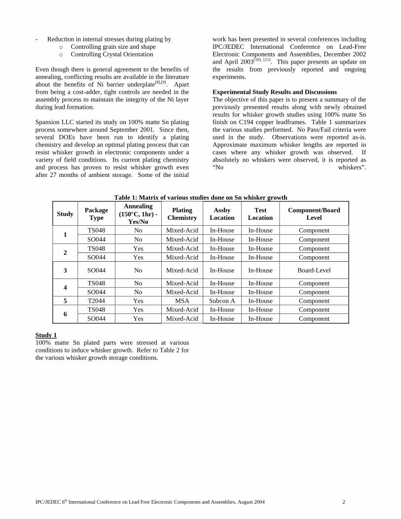
Even though there is general agreement to the benefits of annealing, conflicting results are available in the literature about the benefits of Ni barrier underplate[8],[9]. Apart from being a cost-adder, tight controls are needed in the assembly process to maintain the integrity of the Ni layer during lead formation. Spansion LLC started its study on 100% matte Sn plating process somewhere around September 2001. Since then, several DOEs have been run to identify a plating chemistry and develop an optimal plating process that can resist whisker growth in electronic components under a variety of field conditions. Its current plating chemistry and process has proven to resist whisker growth even after 27 months of ambient storage. Some of the initial
work has been presented in several conferences including IPC/JEDEC International Conference on Lead-Free Electronic Components and Assemblies, December 2002 and April 2003[10], [11]. This paper presents an update on the results from previously reported and ongoing experiments. Experimental Study Results and Discussions The objective of this paper is to present a summary of the previously presented results along with newly obtained results for whisker growth studies using 100% matte Sn finish on C194 copper leadframes. Table 1 summarizes the various studies performed. No Pass/Fail criteria were used in the study. Observations were reported as-is. Approximate maximum whisker lengths are reported in cases where any whisker growth was observed. If absolutely no whiskers were observed, it is reported as “No whiskers”.
Table 1: Matrix of various studies done on Sn whisker growth
Study Package Type
Annealing (150°C, 1hr) -
Yes/No
Plating Chemistry
Assby Location
Test Location
Component/Board Level
TS048 No Mixed-Acid In-House In-House Component 1 SO044 No Mixed-Acid In-House In-House Component TS048 Yes Mixed-Acid In-House In-House Component 2 SO044 Yes Mixed-Acid In-House In-House Component
3 SO044 No Mixed-Acid In-House In-House Board-Level
TS048 No Mixed-Acid In-House In-House Component 4 SO044 No Mixed-Acid In-House In-House Component
5 T2044 Yes MSA Subcon A In-House Component TS048 Yes Mixed-Acid In-House In-House Component
6 SO044 Yes Mixed-Acid In-House In-House Component
Study 1 100% matte Sn plated parts were stressed at various conditions to induce whisker growth. Refer to Table 2 for the various whisker growth storage conditions.

IPC/JEDEC 6th International Conference on Lead Free Electronic Components and Assemblies, August 2004 3
Table 2: Whisker Growth Storage Conditions Condition Storage Condition
1 Temp. cycle (-65 to 150°C) 1000 cycles 2 SPP (121°C, 2 atm, 100%RH) 168 hrs. 3 SPP (121°C, 2 atm, 100%RH) 500 hrs. 4 Storage at 50-55°C, high % RH, 6 months 5 Leave in 20-25°C, 40-65% RH, 2 months 6 Leave in 20-25°C, 40-65% RH, 4 months 7 Leave in 20-25°C, 40-65% RH, 6 months 8 Leave in 20-25°C, 40-65% RH, 8 months 9 Leave in 20-25°C, 40-65% RH, 12 months
10 Leave in 20-25°C, 40-65% RH, 15 months 11 Leave in 20-25°C, 40-65% RH, 24 months 12 Leave in 20-25°C, 40-65% RH, 27 months 13 Store in dry pack, 6 months 14 50°C dry baking, 15 months
Leadframe Material: C194 Grain Size: 3-5 um Thickness: Minimum10 uinches Study Sample size: 30 units of each package type tested
Inspection Method: – 100% units inspected visually at 50X for whisker
growth and grain structure. – Min. 2000X SEM inspection on minimum 3 units, 3
leads per unit. Refer to Figure 1 for SEM images showing the grain structure after various conditions.
Fresh Condition #1
Condition #2 Condition #3

IPC/JEDEC 6th International Conference on Lead Free Electronic Components and Assemblies, August 2004 4
Condition #4 Condition #5
Condition #6 Condition #7
Condition #8 Condition #9
Condition #10 Condition #11

IPC/JEDEC 6th International Conference on Lead Free Electronic Components and Assemblies, August 2004 5
Condition #12 Condition #13
Condition #14 Figure 1: Grain structure after various storage conditions (2000X, Non-annealed parts)
Results: No whiskers or significant grain structure changes were observed on any of the samples stored at all conditions. Study 2 Post Annealing Whisker Growth Study Annealing after plating has become a widely accepted whisker mitigation technique. As a result, annealing at 150°C for 1 hour within 1 hour of plating was introduced in our Pb-free assembly process even though our internal
studies showed no whiskers for samples without annealing (Refer to Study 1). This study was, therefore, done to assess the impact of annealing on whisker growth. Refer to Table 3 for the various whisker growth storage conditions.
Table 3: Whisker Growth Storage Conditions for Annealed parts
Condition Storage Condition 1 Leave in 20-25°C, 40-65% RH, 6 months 2 Leave in 20-25°C, 40-65% RH, 12 months 3 Leave in 20-25°C, 40-65% RH, 24 months 4 Leave in 20-25°C, 40-65% RH, 27 months
Leadframe Material: C194 Grain Size: 3-5 um Thickness: Minimum 10 uinches Study Sample size: 10 units of each package type tested
Inspection Method: – 100% units inspected visually at 50X for whisker
growth and grain structure. – Min. 2000X SEM inspection on minimum 3 units, 3
leads per unit. Refer to Figure 2 for SEM images showing the grain structure after various conditions.

IPC/JEDEC 6th International Conference on Lead Free Electronic Components and Assemblies, August 2004 6
Condition #1 Condition #2
Condition #3 Condition #4
Figure 2: Grain structure after various storage conditions (2000X, Annealed parts) Results: No whiskers or significant grains structure changes were observed on any of the samples stored at all conditions. Monthly Monitor Whisker Growth Study Starting December 2003, annealing step was added to the ongoing monthly monitor program, which is described below: - 1-2K units of each package type are plated every
week. - 100% inspection (using 50X magnification) is done
after plating. - All units are stored at 20-25C/40-65%RH storage
conditions. - 300 units are taken out every month to check for any
whisker growth. Inspection is done on all leads using 40X magnification.
- 5 units, 3 leads per unit are randomly selected and inspected using 2000X SEM.
Results: Till date, data has been collected for annealed samples up to 6 months of storage. No whiskers have been observed so far. Study will continue up to 24 months of storage. Study 3 Daisy chain samples of SO044 package were used to perform Board Level reliability test. 1. 5 mm thick
double-sided boards with OSP finish were used. Automotive under-hood test condition (-40/125°C, 10 sec transition, 30 mins dwell, 24 cycles/day) was used. Refer to Table 4 for the test matrix. After the completion of the temperature cycle test, boards were stored at ambient conditions for whisker monitoring. Leadframe Material: C194 Grain Size: 3-5 um Thickness: Minimum 10 uinches Study Sample Size: 32 units per leg Inspection Method: - 2000X SEM on 3 units per leg, 3 leads per unit Results: - All units passed up to 2000 cycles at which point the
test was stopped. - Whisker inspection was done after completion of
temperature cycle. No whiskers were found on any of the legs.
- Whiskers were monitored again after approx. 22 months of ambient storage. Refer to Table 4 for the results of whisker inspection.

IPC/JEDEC 6th International Conference on Lead Free Electronic Components and Assemblies, August 2004 7
Table 4: Test Matrix and Results for Study 3
Leg Plating Solder Paste Stress Test History Whisker Inspection Result
A Sn Sn 2000 TC + 22 months of ambient storage
Whiskers Found. Figure 3. ~ Max. whisker length of 26 um
B SnPb SnPb 2000 TC + 22 months of ambient storage
Whiskers Found. Figure 4. ~ Max. whisker length of 10 um
C Sn SnPb 2000 TC + 22 months of ambient storage
Whiskers Found. Figure 5. ~ Max. whisker length of 18 um
D SnPb Sn 2000 TC + 22 months of ambient storage
Whiskers Found. Figure 6. ~ Max. whisker length of 20 um
Figure 3 Leg A whisker Inspection Result (~ Max. whisker length seen 26 um)
Figure 4 Leg B whisker Inspection Result (~ Max. whisker length seen 10 um)

IPC/JEDEC 6th International Conference on Lead Free Electronic Components and Assemblies, August 2004 8
Figure 5 Leg C whisker Inspection Result (~ Max. whisker length seen 18 um)
Figure 6 Leg D whisker Inspection Result (~ Max. whisker length seen 20 um)
Both 100% matte Sn and SnPb plated parts with Sn and SnPb solder paste showed the presence of whiskers. As expected, the longest and the maximum number of whiskers were observed in 100% matte Sn plated parts, assembled with Sn solder paste. However, the maximum whisker length found was only approx. 26 um (length/width >2). It has been demonstrated that even 90/10 Sn/Pb deposits will generate growths during thermal cycling. Consumers and industry consortia groups have come to the conclusion that obtaining a "whisker-free" pure tin deposit is simply not feasible particularly given the fact that 90/10 Sn/Pb deposits will form whiskers under certain of the industry-defined whisker test conditions[12]-
[15]. Instead the focus has shifted to defining a maximum acceptable whisker length that does not represent a reliability issue, and the specification being proposed most commonly in this regard is 50 microns. The growths observed in the experiment above are well less than 50 microns and even though the growth is classified
as a “whisker” (per NEMI criteria[16]), it should not a reliability risk in the field. Moreover, 2000 temperature cycles followed by 22 months of ambient storage is far greater than the expected life of the product. Study 4 The objective of this study was multifold – 1. To understand the effect of plating additive
concentration and plating bath temperature on grain structure and size.
2. To identify a process setting combination which can yield SnPb “work-like” grain structure.
3. To study the effect of the plating parameters on whisker growth.
Refer to Table 5 for the details of the various legs for the experiment with corresponding whisker growth results. A current density of 124 Amps/Sq. ft. was used for all legs.

IPC/JEDEC 6th International Conference on Lead Free Electronic Components and Assemblies, August 2004 9
Table 5: Study 4 Experiments: Conditions and Results Leg Package Additive
Conc. Temp. Grain Size Thickness
(uinches)Visual Inspection
after plating Whisker Growth (leave
t 20-25C, 40-65%RH for 12 months)
Whisker Growth (leave at 20-25C, 40-65%RH for 24
months)
SO 44 0. 00% 80 F Large 459
Rough deposit, Nodules No whisker observed
~ Max. whisker length 36um
1
TS 48 0. 00% 80 F Large 477
Rough deposit, Nodules No whisker observed
~ Max. whisker length 20um
SO 44 0. 00% 110 F Large 529
Rough deposit, Nodules No whisker observed
~ Max. whisker length 4 um.
2
TS 48 0. 00% 110 F Large 459
Rough deposit, Nodules No whisker observed
~ Max. whisker length 24um
SO 44 2. 00% 80 F Fine 353
Smooth deposit, Few Nodules No whisker observed
No whisker observed
3
TS 48 2. 00% 80 F Fine 301
Smooth deposit, Few Nodules No whisker observed
~ Max. whisker length 28um
SO 44 2. 00% 110 F Fine 446 Smooth deposit No whisker observed
~ Max. whisker length 13um
4
TS 48 2. 00% 110 F Fine 457 Smooth deposit No whisker observed
~ Max. whisker length 10um
SO 44 4. 00% 80 F Fine 328 Smooth deposit No whisker observed
~ Max. whisker length 16um
5
TS 48 4. 00% 80 F Fine 392 Smooth deposit No whisker observed
~ Max. whisker length 4um
SO 44 4. 00% 110 F Fine 480 Smooth deposit No whisker observed
No whisker observed
6
TS 48 4. 00% 110 F Fine 404 Smooth deposit No whisker observed
No whisker observed
Leadframe Material: C194 Grain Size: 3-5 um Thickness: Minimum 10 uinches Study Sample size: 10 units of each package type tested Inspection Method - 2000X SEM, 10 leads/3 units Results:
1) Grain structure and size becomes fine as the additive concentration increases. Plating
temperature does not seem to have a significant effect on grain structure or size.
2) Deposited plating becomes smoother and with fewer nodules with increasing additive concentration and plating temperature.
3) None of the process settings tried yielded the “worm-like” SnPb grain structure.
4) Resistance to whisker growth appeared to be proportional to additive concentration and plating temperature. Best whisker growth results were observed with 4% additive concentration at 110F. Refer to Figure 7 for pictures after 24 months of ambient storage.

IPC/JEDEC 6th International Conference on Lead Free Electronic Components and Assemblies, August 2004 10
Leg 1: 0%, 80F
SO044 (Hillocks or Lumps) TS048 (Hillocks)
Leg 2: 0%, 110F
SO044 (Striations Whisker) TS048 (Initiating from Hillock)
Leg 3: 2%, 80F
SO044 (No whisker) TS048 (Needle Whisker)

IPC/JEDEC 6th International Conference on Lead Free Electronic Components and Assemblies, August 2004 11
Leg 4: 2%, 110F
SO044 (Striations Whisker) TS048 (Striations Whisker)
Leg 5: 4%, 80F
SO044 (Rings Whisker) TS048 (Hillock)
Leg 6: 4%, 110F
SO044 (No whisker) TS048 (No whisker)
Figure 7: Whisker Growth Inspection Results after 24 months of storage Study 5 To correlate the subcon provided results with our own internal study, subcon A assembled Type 2 TSOP, T2044,
package was stored at 20-25°C, 40-65%RH. 8 months of storage have been completed till now.

IPC/JEDEC 6th International Conference on Lead Free Electronic Components and Assemblies, August 2004 12
Leadframe Material: C7025 Grain Size: 5 to 10 um Thickness: average 400 uinches Sample size: 150 units
Inspection Method: - 3000X SEM for 3 units, 3 leads per unit. Refer to Figure 8 for the typical grain structure observed.
Figure 8: Typical grain structure for Subcon A after 8 months of storage
Result: No whiskers were observed on any of the samples. Further study is ongoing. Study 6 Since most of the above studies started way before any standards/recommendations existed for accelerated whisker test conditions, a new study was initiated to reconcile the results obtained earlier with NEMI recommended test conditions and inspection criteria[16]. Refer to Table 6 for the experiment matrix. Samples were assembled using the existing Pb-free assembly process, which includes annealing after plating.
A control leg with 85Sn15Pb plating was also run in parallel for comparison. Leadframe Material: C194 Grain Size: 3-5 um Thickness: Minimum 10 uinches Sample size: Refer to Table 6 Inspection Method: - 40X visual inspection on 100% units after every
readpoint. - SEM inspection - 300X (all leads for 3 units), 1000X
and 2000X (3 leads per unit for 3 units) at every readpoint.

IPC/JEDEC 6th International Conference on Lead Free Electronic Components and Assemblies, August 2004 13
Table 6: Sample Size and Inspection Results for various readpoints Package TS048 SO044 Plating Sn Sn SnPb Sn Sn SnPb Annealing Yes No No Yes No No
JEDEC Level 3 + Temp Cycle (-40C to 150C, 3 cycles/hour) 1000 cycles 320, No 320, No 160, No 320, No 320, No 160, No JEDEC Level 2A + Temp Cycle (-40C to 150C, 3 cycles/hour) 500 cycles 320, No 320, No 160, No 320, No 320, No 160, No JEDEC Level 3 + HAST (130C/85%RH, Biased) 96 hours 27, No 30, No 15, No High Temperature Storage (150C) 500 hours 100, No 100, No 50, No
High Temperature Operating Life (150C, Biased) 500 hours 60, No 60, No 30, No
NEMI Temp Cycle (-55C to 85C, 3 cycles/hour) 1000 cycles
200, Mounds
(Figure 9. 1)
200, Whiskers
(Figure 10. 1) 100, No
204, Mounds
(Figure 9. 2)
204, Mounds
(Figure 10. 2)
102, No (Figure 11)
NEMI Temp Humidity (60C/93%RH) 1000 hours 200, No 200, No 100, No 200, No
(Figure 12) 200, No
(Figure 13)100, No
(Figure 14)
NEMI Ambient Storage (Air-Conditioned Facility)
3 months (continue upto 24 months) 540, No 542, No 272, No 601, No 597, No 308, No Note: “No” in the table above denotes “No Whiskers”.
300X 2000X
Figure 9. 1: SEM after 1000 TC of NEMI Condition on Pb-free Annealed parts

IPC/JEDEC 6th International Conference on Lead Free Electronic Components and Assemblies, August 2004 14
300X 2000X
Figure 9. 2: SEM after 1000 TC of NEMI Condition on Pb-free Annealed parts
300X 2000X
Figure 10. 1: SEM after 1000 TC of NEMI Condition on Pb-free Non-Annealed parts (Maximum Whisker
Length ~ 20 um)
300X 2000X
Figure 10. 2: SEM after 1000 TC of NEMI Condition on Pb-free Non-Annealed parts

IPC/JEDEC 6th International Conference on Lead Free Electronic Components and Assemblies, August 2004 15
300X 2000X
Figure 11: SEM after 1000 TC of NEMI Condition on SnPb Non-Annealed parts
300X 2000X
Figure 12: SEM after 1000 TH of NEMI Condition on Pb-free Non-Annealed parts
300X 2000X
Figure 13: SEM after 1000 TH of NEMI Condition on Pb-free Non-Annealed parts

IPC/JEDEC 6th International Conference on Lead Free Electronic Components and Assemblies, August 2004 16
300X 2000X
Figure 14: SEM after 1000 TH of NEMI Condition on Pb-free Non-Annealed parts
Results and Discussions: 1. NEMI recommended temperature cycle condition
seems to be more effective at accelerating whisker growth. However, it could also be due to the lack of reflow (during preconditioning) prior to NEMI tests as compared to 3 times reflow for the other temperature cycle condition. Reflow could have acted as an annealing step for the samples and hence increased their resistance for whisker growth. NEMI tests with reflow will be conducted in near future.
2. Whiskers were observed on non-annealed parts under NEMI Temperature Cycling test. Short growths were observed in annealed samples that underwent NEMI recommended accelerated temperature cycle condition. The short growths observed are defined as "mounds". They are not Sn whiskers. Mostly, the growths observed were less than 5 microns in length. The compressive stress effect in the tin deposit, which is generated by temperature cycling, is a result of the CTE mismatch between the copper alloy substrate and the Sn deposit, i. e. , 17 vs. 23 ppm/deg K respectively. As the temperature cycling proceeds, the difference in the rates of expansion (during heating) and contraction (during cooling) of the Sn and copper generates the compressive stress that is the driving force for Sn whisker growth. The normal response for a whisker-resistant matte Sn coating when subjected to these types of compressive stresses is the formation of the small mounds observed in the study.
3. Annealing seems to be effective in retarding whisker growth under NEMI recommended accelerated testing conditions.
Conclusions Most of the subcontractor houses have chosen 100% matte Sn as their Pb-free alternative after their own internal whisker growth studies. In addition, there are numerous references of technical papers and other publications from individual researchers, companies and industry consortiums that show results similar to the ones obtained above with pure Sn on Cu leadframes using different chemistries and plating processes[16]-[20].
From the review of the existing data from other sources and internal results obtained in all the studies so far, it is clear that 100% matte Sn on Cu leadframes can be a whisker resistant Pb-free alternative, if the right plating chemistry and plating process is chosen. 100% matte Sn plated Pb-free parts have proven to be whisker growth resistant under a variety of extensive stress test conditions done up to date and hence can be expected to produce whisker free assemblies in the field. Ongoing and Future Work Currently, various studies are ongoing and under planning. Some of the major ones are listed below. - Perform NEMI recommended accelerated whisker
growth tests on samples after 24 months of ambient storage.
- Perform NEMI recommended accelerate whisker growth tests on samples after Preconditioning (JEDEC Level 3 and JEITA Rank ‘E’).
- Perform NEMI recommended accelerate whisker growth tests on subcon assembled parts.
- Repeat Board Level Reliability studies on Pb-free assemblies.
- Identify an optimal time and temperature for effective annealing post plating.
The results from these studies will be presented as and when available, in future conferences. Acknowledgements We would like to extend a debt of gratitude to our management and peers for their support and encouragement through this work. We would like to extend a special thanks to our Reliability Labs, Device Analysis Labs, Prasit Juntui, Nitis Niyomyatra, Jiraporn Tondtan, Dr. Yong Du, Jeff Pollock, Kevin Depetrillo, Francis Classe and the entire plating process engineering team for their kind and timely support.

IPC/JEDEC 6th International Conference on Lead Free Electronic Components and Assemblies, August 2004 17
References [1] Tu et al, Structure and Kinetics of Sn Whisker Growth on Pb-Free Solder Finish, 52 Electronic Component & Technology Conference Proceedings, CA, 2002. [2] A Egli, et al, Where Crystal Planes Meet: Contribution to the Understanding of the Tin Whisker Growth Process, IPC Annual Meeting, November 2002. [3] W. J. Choi, et al, Structure and Kinetics of Sn Whisker Growth on Pb-free Solder Finish, Proceedings of IEEE Electronic Components and Technology Conference, 2002. [4] C. Xu et al, Understanding Whisker Phenomenon: Driving Force for Whisker Formation, CALCE Lead-Free Forum, University of Maryland, October 10, 2002, College Park, MD. [5] R. Schetty et al, Lead-Free Finishes Whisker Studies and Practical Methods for Minimizing the Risk of Whisker Growth, Shipley report. [6]. R. Schetty, Whisker Growth Studies. Proceedings of IPC Annual Meeting, October 2001. [7] R. Schetty, Tin Whisker Growth & the Metallurgical Properties of Electrodeposited Tin, Proceedings of the IPC/JEDEC Conference, May 2002. [8] J. W. Osenbach et. al. , The Effects of Board Attachment Processing on Sn Whisker Formation on Electroplated Matte-Sn on Cu Alloy Lead Frames, Proceedings of IPC/JEDEC Fifth International Conference on Lead-Free Electronic Components and Assemblies, March 2004. [9] S. Prasad, NEMI Sn Whiskers Standards Committee Status, Apex 2002. http://www. promax. dk/download/data/Leadfree/Seminar%2005-2004/YAGEO%20Leadfree/Information/whisker%20APEX_2002_rev8. pdf [10] A. Sriyarunya, Lead-free plating on Integrated circuit, Proceedings of IPC/JEDEC International Conference on Lead-Free Electronic Components and Assemblies, December 2002.
[11] A. Sriyarunya, R. Schetty, Lead-free plating of Semiconductor Devices-Qualification & Manufacturability study, Proceeding of IPC/JEDEC Third Annual International Conference on Lead-Free Electronic Components and Assemblies, April 2003. [12] J. Brusse, Whiskers of Tin-Lead (Sn-Pb) on REFLOWED Die Attach Solder Used in the Manufacture of a Laser Diode Array, NASA, December 2003. http://nepp. nasa. gov/whisker/reference/tech_papers/Leidecker2003-SnPb-whiskers-on-laser-diode-array. pdf [13] S. Winkler and B. Hom, A Look at the Past Reveals a Leadfree Drop-in Replacement, HDI on-line, March 2001. [14] K. Cunningham and M. Donahue, Thin Whiskers: Mechanisms of Growth and Prevention, Proceedings 4th International SAMPE Electronics Conference, June 1990. [15] R. Schetty, Minimization of Tin Whisker Formation for Lead Free Electronics Finishing, Proceedings IPC Works Conference, 2000. [16] NEMI Tin Whisker research activities http://www. nemi. org/projects/ese/tin_whisker_activities. html [17] P. Oberndoff, et. al. , Whisker Formation on Sn Plating, Proceedings of IPC/JEDEC Fifth International Conference on Lead-Free Electronic Components and Assemblies, March 2004. [18] http://www. statsus. com/stts/pages/page. asp?SID=4&PageID=220 [19] http://www. aitbatam. com/leadfree/leadfree. html [20] A. Elgi, et al, New Approaches to Whisker Free Tin Deposits, Electronics Packaging Technology, 2003 5th Conference (EPTC 2003) , 10-12 Dec. 2003.