Erratum to: Light induced silver and copper plating on silver screen-printed contacts of silicon...
6
Light induced silver and copper plating on silver screen-printed contacts of silicon solar cells S. TUTASHKONKO *1,2 , A. KAMINSKI−CACHOPO 1 , C. BOULORD 1 , R. ARéS 2 , V. AIMEZ 2 , and M. LEMITI 1 1 Institut des Nanotechnologies de Lyon INL−UMR5270, Université de Lyon, CNRS, INSA de Lyon, Villeurbanne, F−69621, France 2 CRN2, Université de Sherbrooke Sherbrooke, Québec, Canada J1K 2R1 In this paper we present the results of solar cell’s screen printed contacts thickening by light induced plating (LIP) of Cu and Ag. Light−induced and light−assisted plating techniques are compared. Plating bath current versus illumination intensity, the potentials of metallic anode, front and back surfaces of the solar cell were measured and analyzed for all possible plating modes. The current−voltage behaviour of cells under illumination in a plating bath for the cases of electrically insulated and non−insulated back−surface of a cell is analyzed and discussed. Finally, the exact values of current/voltage/illumination in− tensity for optimal depositions and a general recipe for their determination for different plating materials are given. The quality of deposited layers, state of contact−line and anti−reflective coating surface were controlled after plating by cross−section and planar−view SEM observations. The electrical properties of plated contacts and their effect on overall effi− ciency of solar cell were investigated by measuring contact−line resistance and dark− and light I–V solar cell measurements. The absence of short−circuits was verified by imaging with an infra−red camera. Keywords: light−induced plating, screen−printing, solar cells. 1. Introduction One of the most promising metallization techniques for replacing the screen−printing method for the purposes of increasing solar cell efficiency is called light induced plat− ing (LIP) [1]. Being a derivative of electroplating, LIP exploits the photovoltaic properties of solar cells to produce a sufficient current to plate its own contact grid with high conductivity metal [2–4]. As the metallic cations in the plat− ing bath have a positive charge, the ability of a p−type illu− minated solar cell to accumulate positive charge on its back surface and negative charge on its front surface makes LIP simple in realization and close to be an industrial produc− tion, contact deposition technique. The manufacturing ready LIP process lines that exist on the market today, can be attractive for solar cells manufacturing company’s capital equipment expenditures. Besides lump sum equipment investments, however, the direct expenses of entire plating processes such as consum− able supplies costs are also important. A quick calculation shows that the mass of pure silver plated onto the front sur− face of a 125×125 mm−sized solar cell is roughly 0.15 g. Moreover, attempts at direct silver to silicon plating meet with low deposited layer adherence, high interface resistivity and metal−to−semiconductor diffusion. Plating over pre−existing seed/barrier layers of Ni, Pt or Ti created by sputtering or electroless plating often followed by ther− mal annealing, aims to solve the indicated problems [5,6] but introduces the necessity of additional processing stages for a solar cells fabrication. The best industrial silicon solar cells produced with the conventional silver screen−printing technique have a fill fac− tor value above 80%. Therefore the possible gain from using electroplating can hardly justify the additional ex− penses of implementation of the plating process into the production cycle. In this paper we propose a functional and cost−effec− tive way for the perceptible improvement in contact grid resis− tivity (and thus overall solar cell efficiency) by light−assisted plating of a thin (compared to the thickness of screen−printed contacts) layer of copper or silver onto the surface of existing screen printed contacts. 2. Experimental For the experiments, industrial 125×125 mm p−type silicon solar cells were used (cells were kindly provided by Pho− towatt International S.A.S. company). To analyze the influ− ence of a shadowing effect from the deposited layer on the cell efficiency, cells with different “finger” spacings were used. The tests using cells with fine−line printing were also done. For the plating tests, the cells were cut into 40×60 mm Opto−Electron. Rev., 19, no. 3, 2011 S. Tutashkonko OPTO−ELECTRONICS REVIEW 19(3), 301–306 DOI: 10.2478/s11772−011−0030−6 * e−mail: sergii.tutashkonko@insa−lyon.fr
-
Upload
usherbrooke -
Category
Documents
-
view
1 -
download
0
Transcript of Erratum to: Light induced silver and copper plating on silver screen-printed contacts of silicon...

Light induced silver and copper plating on silver screen-printed contactsof silicon solar cells
S. TUTASHKONKO*1,2, A. KAMINSKI−CACHOPO1, C. BOULORD1, R. AR�S2, V. AIMEZ2,and M. LEMITI1
1Institut des Nanotechnologies de Lyon INL−UMR5270, Université de Lyon, CNRS, INSA de Lyon,Villeurbanne, F−69621, France
2CRN2, Université de Sherbrooke Sherbrooke, Québec, Canada J1K 2R1
In this paper we present the results of solar cell’s screen printed contacts thickening by light induced plating (LIP) of Cu andAg. Light−induced and light−assisted plating techniques are compared. Plating bath current versus illumination intensity, thepotentials of metallic anode, front and back surfaces of the solar cell were measured and analyzed for all possible platingmodes. The current−voltage behaviour of cells under illumination in a plating bath for the cases of electrically insulated andnon−insulated back−surface of a cell is analyzed and discussed. Finally, the exact values of current/voltage/illumination in−tensity for optimal depositions and a general recipe for their determination for different plating materials are given.
The quality of deposited layers, state of contact−line and anti−reflective coating surface were controlled after plating bycross−section and planar−view SEM observations. The electrical properties of plated contacts and their effect on overall effi−ciency of solar cell were investigated by measuring contact−line resistance and dark− and light I–V solar cell measurements.The absence of short−circuits was verified by imaging with an infra−red camera.
Keywords: light−induced plating, screen−printing, solar cells.
1. Introduction
One of the most promising metallization techniques forreplacing the screen−printing method for the purposes ofincreasing solar cell efficiency is called light induced plat−ing (LIP) [1]. Being a derivative of electroplating, LIPexploits the photovoltaic properties of solar cells to producea sufficient current to plate its own contact grid with highconductivity metal [2–4]. As the metallic cations in the plat−ing bath have a positive charge, the ability of a p−type illu−minated solar cell to accumulate positive charge on its backsurface and negative charge on its front surface makes LIPsimple in realization and close to be an industrial produc−tion, contact deposition technique. The manufacturing readyLIP process lines that exist on the market today, can beattractive for solar cells manufacturing company’s capitalequipment expenditures.
Besides lump sum equipment investments, however, thedirect expenses of entire plating processes such as consum−able supplies costs are also important. A quick calculationshows that the mass of pure silver plated onto the front sur−face of a 125×125 mm−sized solar cell is roughly 0.15 g.
Moreover, attempts at direct silver to silicon platingmeet with low deposited layer adherence, high interfaceresistivity and metal−to−semiconductor diffusion. Plating
over pre−existing seed/barrier layers of Ni, Pt or Ti createdby sputtering or electroless plating often followed by ther−mal annealing, aims to solve the indicated problems [5,6]but introduces the necessity of additional processing stagesfor a solar cells fabrication.
The best industrial silicon solar cells produced with theconventional silver screen−printing technique have a fill fac−tor value above 80%. Therefore the possible gain fromusing electroplating can hardly justify the additional ex−penses of implementation of the plating process into theproduction cycle.
In this paper we propose a functional and cost−effec−tive way for the perceptible improvement in contact grid resis−tivity (and thus overall solar cell efficiency) by light−assistedplating of a thin (compared to the thickness of screen−printedcontacts) layer of copper or silver onto the surface of existingscreen printed contacts.
2. Experimental
For the experiments, industrial 125×125 mm p−type siliconsolar cells were used (cells were kindly provided by Pho−towatt International S.A.S. company). To analyze the influ−ence of a shadowing effect from the deposited layer on thecell efficiency, cells with different “finger” spacings wereused. The tests using cells with fine−line printing were alsodone. For the plating tests, the cells were cut into 40×60 mm
Opto−Electron. Rev., 19, no. 3, 2011 S. Tutashkonko 301
OPTO−ELECTRONICS REVIEW 19(3), 301–306
DOI: 10.2478/s11772−011−0030−6
*e−mail: sergii.tutashkonko@insa−lyon.fr

pieces (with one bus bar), and long stripes with two busbars, so that one can measure the finger line resistivitybefore and after a metal deposition. To avoid the short cir−cuit of the solar cell by the electrolyte, the boards were elec−trically insulated. To measure the potential distribution, thevoltage between the front side, rear side, and anode weremeasured by the multimeters as shown in Fig. 1. The platingcurrent was controlled by the ammeter connected betweenthe anode and the rear side of the cell. For light−assistedplating experiments an external current source was used.
3. Results
3.1. Electrolyte characterizationPlating bath analysis methods were developed for copperand silver electrolytes. For copper plating, copper sulfidebased electrolytes and for silver plating, two different non−−cyanide alkaline commercial plating solutions were used.
As the idea of LIP derives from the electrodepositionmethod, the electrochemical reactions taking place on bothanodic and cathodic sites are similar. But our search for theoptimal plating conditions has highlighted some LIP spe−cific problems.
First, we measured the I–V of the electrolytes in order todetermine the plating bath resistivity, the plating currentvariation range. The results of these measurements areshown in Fig. 2.
The current curve is expected to have saturation whenthe high current in the bath is limited by the electrolyte.However, the I–V curve for the copper bath bends visibly atthe high current region [Fig. 2(a)]. Before current saturation,a parasitic reaction begins in the electrolyte and the currentincreases suddenly. At the same time, both the anode andthe cathode are covered by a black flake−like product of theparasitic reaction. The minimal resistance of 5 �cm2 isfound at the upper half of the current range. It is dangerousto work close to the limit current as a sudden fluctuation can
Light induced silver and copper plating on silver screen−printed contacts of silicon solar cells
302 Opto−Electron. Rev., 19, no. 3, 2011 © 2011 SEP, Warsaw
Fig. 1. Schematics of experimental setup for copper plating method.
Fig. 2. Current−voltage and resistivity−voltage curves measured forthree copper (a) and silver (b,c) electrolytes used.

lead to irreversible electrolyte contamination. So, a prefera−ble current range is between 4 and 8.5 A/dm2.
Resistance of the first silver plating electrolyte has twominima [Fig. 2(b)], a local minimum at V = 0.2 V, I = 0.4A/dm2 and a global minimum near the upper limit current atV = 1 V, I = 0.98 A/dm2. But the distinction of the silverplating bath is that the current is stable at the whole currentrange, the difference between the maximal and minimalresistance is no more than 20%, while for the copper bath, itis up to 100%.
The second silver plating electrolyte was found to beeven more stable. Its resistivity did not change at the wholerange of currents measured [Fig. 2(c)].
3.2. Cell in bath characterization
In the case of p−type solar cells, the electrical contact withthe solar cell is provided by its rear surface. In the simplestcase, the solar cell rear surface is directly connected with themetallic anode to close the plating bath circuit. When thecell is illuminated, the front surface is at a negative potentialdue to the photovoltaic effect. At the same time, the rear sur−face is charged positively. As the anode is connected withthe rear surface, it is at a positive potential. Thus, the anodematerial will be dissolved and consequently deposited to thecell front surface. The first problem of this LIP realizationresults from its definition. As the rear side potential ishigher than the one at the front side and equals to the anodepotential, this results in the dissolution of the rear side mate−rial and its deposition on the front side [7,8].
A possible way−out is electrical insulation of a solarcell’s rear surface. In this case, the only interface betweena cell and the electrolyte is a solar cell’s front face contactgrid. The plating current is controlled by the ammeter anddepends only on illumination intensity.
Another solution is a transfer to light−assisted platingmethod. The plating current is applied by external currentsource. The potential distribution is adjusted by light illumi−nation intensity in order to fix the voltage VAR between theanode and the cell’s front face equal to the voltage VRF
between the cell’s rear and front sides. In this case, a rate ofoxidation and reduction processes at the cell’s rear surfaceis in equilibrium. Thus, the rear surface is untouched duringthe plating process, while the front surface is being plated.
First of all, the I–V measurements of the solar cell in thecopper plating bath for different illumination intensitieswere done (Fig. 3). I–V curves resemble the ones obtainedin the case of a solar cell in air. The working region is still atthe saturation zone of the solar cell I–V curve, described bythe diode equation. The saturation current increases withillumination intensity. However, there are some prominentdistinctions. The “fill factor” increases while illuminationintensity is grown, but the open−circuit voltage falls. At thesaturation zone, the current rises up exponentially, startingfrom a certain voltage V2. This voltage V2 is 0 for the darkI–V curves and moves to positive voltages for more illu−minated cells.
In Fig. 4, the results of V2(V3) measurements are pre−sented. The curves are linear and they change their incline ata certain voltage V2. This voltage depends on the illumina−tion intensity and corresponds to the open−circuit voltagefrom I–V measurements. As the cell illumination is incre−ased, its V2(V3) curve becomes saturated.
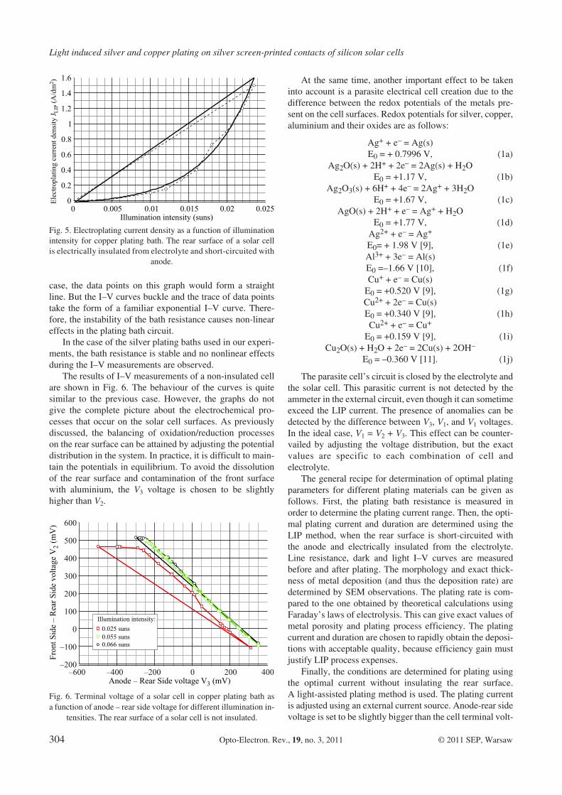
To investigate these phenomena, the plating current asa function of illumination intensity was measured. In thisexperiment, the rear side of the solar cell is still insulatedfrom electrolyte and short−circuited with the anode. Noexternal power supplies are used. The current grows expo−nentially, thus not linearly (Fig. 5). As follows from theequivalent circuit, the current measured by the ammeter isnot Icc but the current of the solar cell, charged by the bathresistance. This resistance is non−linear as shown in Fig. 2.In the absence of the external voltage V3, the terminal vol−tage V2 depends linearly on the illumination intensity(Fig. 4). So, in this case, we are not measuring the platingcurrent, but a terminal voltage proportional to the lightintensity. If the bath resistance was stable, the saturationbranches of the I–V curves (Fig. 3) would be flat. In this
Opto−Electron. Rev., 19, no. 3, 2011 S. Tutashkonko 303
Fig. 3. I–V of a solar cell in a copper plating bath, for different illu−mination intensities. The rear surface of a solar cell is insulated from
electrolyte.
Fig. 4. Terminal voltage of a solar cell in a copper plating bath asa function of anode – rear side voltage for different illumination in−tensities. The rear surface of a solar cell is insulated from electrolyte.
case, the data points on this graph would form a straightline. But the I–V curves buckle and the trace of data pointstake the form of a familiar exponential I–V curve. There−fore, the instability of the bath resistance causes non−lineareffects in the plating bath circuit.
In the case of the silver plating baths used in our experi−ments, the bath resistance is stable and no nonlinear effectsduring the I–V measurements are observed.
The results of I–V measurements of a non−insulated cellare shown in Fig. 6. The behaviour of the curves is quitesimilar to the previous case. However, the graphs do notgive the complete picture about the electrochemical pro−cesses that occur on the solar cell surfaces. As previouslydiscussed, the balancing of oxidation/reduction processeson the rear surface can be attained by adjusting the potentialdistribution in the system. In practice, it is difficult to main−tain the potentials in equilibrium. To avoid the dissolutionof the rear surface and contamination of the front surfacewith aluminium, the V3 voltage is chosen to be slightlyhigher than V2.
At the same time, another important effect to be takeninto account is a parasite electrical cell creation due to thedifference between the redox potentials of the metals pre−sent on the cell surfaces. Redox potentials for silver, copper,aluminium and their oxides are as follows:
Ag+ + e– = Ag(s)E0 = + 0.7996 V, (1a)
Ag2O(s) + 2H+ + 2e– = 2Ag(s) + H2OE0 = +1.17 V, (1b)
Ag2O3(s) + 6H+ + 4e– = 2Ag+ + 3H2OE0 = +1.67 V, (1c)
AgO(s) + 2H+ + e– = Ag+ + H2OE0 = +1.77 V, (1d)
Ag2+ + e– = Ag+
E0= + 1.98 V [9], (1e)Al3+ + 3e– = Al(s)E0 =–1.66 V [10], (1f)Cu+ + e– = Cu(s)
E0 = +0.520 V [9], (1g)Cu2+ + 2e– = Cu(s)E0 = +0.340 V [9], (1h)Cu2+ + e– = Cu+
E0 = +0.159 V [9], (1i)Cu2O(s) + H2O + 2e– = 2Cu(s) + 2OH–
E0 = –0.360 V [11]. (1j)
The parasite cell’s circuit is closed by the electrolyte andthe solar cell. This parasitic current is not detected by theammeter in the external circuit, even though it can sometimeexceed the LIP current. The presence of anomalies can bedetected by the difference between V3, V1, and V1 voltages.In the ideal case, V1 = V2 + V3. This effect can be counter−vailed by adjusting the voltage distribution, but the exactvalues are specific to each combination of cell andelectrolyte.
The general recipe for determination of optimal platingparameters for different plating materials can be given asfollows. First, the plating bath resistance is measured inorder to determine the plating current range. Then, the opti−mal plating current and duration are determined using theLIP method, when the rear surface is short−circuited withthe anode and electrically insulated from the electrolyte.Line resistance, dark and light I–V curves are measuredbefore and after plating. The morphology and exact thick−ness of metal deposition (and thus the deposition rate) aredetermined by SEM observations. The plating rate is com−pared to the one obtained by theoretical calculations usingFaraday’s laws of electrolysis. This can give exact values ofmetal porosity and plating process efficiency. The platingcurrent and duration are chosen to rapidly obtain the deposi−tions with acceptable quality, because efficiency gain mustjustify LIP process expenses.
Finally, the conditions are determined for plating usingthe optimal current without insulating the rear surface.A light−assisted plating method is used. The plating currentis adjusted using an external current source. Anode−rear sidevoltage is set to be slightly bigger than the cell terminal volt−
Light induced silver and copper plating on silver screen−printed contacts of silicon solar cells
304 Opto−Electron. Rev., 19, no. 3, 2011 © 2011 SEP, Warsaw
Fig. 5. Electroplating current density as a function of illuminationintensity for copper plating bath. The rear surface of a solar cellis electrically insulated from electrolyte and short−circuited with
anode.
Fig. 6. Terminal voltage of a solar cell in copper plating bath asa function of anode – rear side voltage for different illumination in−
tensities. The rear surface of a solar cell is not insulated.

age by adjusting the illumination intensity. Voltage balancecan be additionally corrected to compensate the parasiticcell currents, if any. Equilibrium of all three measured volt−ages can be an indicator of the absence or the presence ofparasitic cells.
3.3. Plating results
The most significant impacts on the plating results comefrom the deposition rate and the plating duration. Figure 7represents the analysis of the line (“finger”) resistivity im−provements, as a function of the plating current, for fixeddeposition duration. Reduction of the line resistance leads toan enhancement of the solar cell efficiency, as it depends onthe cell series resistance. The graph has a maximum thatdefines the optimal plating current to be used for the deposi−tions. The first growth part of the plot corresponds to thedeposition thickness increase, the decay part of the plot cor−responds to the losses due to significant layer porosity.Therefore, the optimal plating current is always a compro−mise between the deposition rate and the deposited materialquality. A SEM image of a dense copper layer, depositedunder a current density 2 A/dm2, is shown in Fig. 8. By thesame principle, the optimal currents were measured for allelectrolytes used. The optimal current densities for silverplating electrolytes are 0.28 and 0.6 A/dm2. The platingrates for copper and silver electrolytes under optimalcurrents are 0.5, 0.28, and 0.6 μm/min respectively.
Plating efficiency was found to depend on the printscreen ink composition. For Ag/Al 4% ink, used for the lineresistivity improvements, the best results were obtainedwith a composition between 60% and 75%, for Ag/Al 2%this value varied between 35% and 60%. It should be noted,that the absolute value of line resistivity is smaller for theink with the larger silver content. However, the line resisti−vity of Ag/Al 4% screen−printed contacts with only 2 μm ofdeposited copper is of the same order as the screen−printedline with the 100% silver ink.
The solar cell efficiency gain is found to be a non−monotonic function of deposition duration. The contact lineresistance decreases as the contact thickens but at the certainmoment the entire cell efficiency falls due to the shadoweffect from a thick layer deposited. A deposition thicknessbetween 2 and 5 μm was found to be sufficient to signifi−cantly reduce the line resistance without creating majorshadowing effects. The cells plated using optimal currentsgained up to 1.53% of absolute efficiency.
4. Conclusions
Light−induced and light−assisted plating methods were stu−died and compared. The major LIP problems of cell rearside dissolution can be solved by either of two ways. Ina first case, the front plating depends only on the illumina−tion intensity, and thus can be used to determine optimalcurrent density and plating duration. This current is thenapplied to the light−assisted plating method, which does notrequire rear surface insulation. This method implies the useof rear surface protection by adjusting the cell potentialswith an external current source, and a light illuminationsource at the same time. It was found, that the equilibrium ofterminal and anode – rear side voltage must be modified tocompensate the parasite cells. The plating current was foundto depend non−linearly on illumination intensity, due to thebath resistance−voltage behaviour. This causes the I–Vcurve to bend at the saturation region. This should be takeninto account while adjusting the rear and front side po−tentials to avoid a back surface dissolution.
While developing the copper plating method for re−search applications, we found that it can also be used as aneffective mean to improve the solar cell characteristics in anindustrial production scheme. If the optimal plating condi−tions are chosen appropriately, the plated copper layers aredense enough and do not diffuse deep into the structure. Thelayers can be protected from oxidation by fine electrolessfinishing.
Opto−Electron. Rev., 19, no. 3, 2011 S. Tutashkonko 305
Fig. 7. Increase in the contact line conductivity as a result of the plat−ing of a copper layer on the cell, as a function of the plating current
density, for a fixed deposition time.
Fig. 8. SEM cross−section image of a dense copper layer depositedon a screen−printed line under 2 A/dm2 current density.

Deposition of only 2 μm of copper can perceptiblyimprove the line resistance and the whole cell efficiency.5−μm deposits can enhance the line conductivity almosttwo−fold. However, the benefits of thicker layers are offsetby the creation of important additional optical losses, due toshadowing effect.
Absolute solar cell efficiency was improved by 1.53%.
References1. A. Mette, C. Schetter, D. Wissen, S. Lust, S.W. Glunz, and
G. Willeke, “Increasing the efficiency of screen−printed sili−con solar cells by light−induced silver plating”, Proc. 12thEur. Photovoltaic Solar Energy Conf., 1056–1059 (2006).
2. L.F. Durkee, “Method of plating by means of light”, US Pat−ent No 4144139, Solarex Corporation, USA, 1979.
3. L.A. Grenon, “Electroplating method”, US Patent No4251327, Motorola, USA, 1980.
4. G.R. Allardyce, K. Bass, and J. Rasch, “Light assisted electroplating process”, European Patent Application EP 1865563A2, Rohm and Haas Electronic Materials, USA, 2007.
5. C. Boulord, A. Kaminski, B. Canut, S. Cardinal, and M.Lemiti, “Electrical and structural characterization of electro−less nickel−phosphorus contacts for silicon solar cell meta−llization”, J. Electrochem. Soc. 157, H742–H745 (2010)
6. C. Boulord, A. Kaminski, Y. Veschetti, and M. Lemiti,“Comparison of different electrochemical deposits for con−tact metallization of silicon solar cells”, Mater. Sci. Eng.B165, 53–56 (2009).
7. A. Mette, “New concepts for the front side metallization ofindustrial silicon solar cells”, PhD Dissertation, Albert−Lud−wigs−Universitat, Freiburg, 2007.
8. J. Bartsch, V. Radtke, C. Schetter, and S.W. Glunz, “Electro−chemical methods to analyse the light−induced plating pro−cess”, J. Appl. Electrochem. 40, 757–765 (2010).
9. A.J. Bard, R. Parsons, and R.J. Jordan, Standard Potentialsin Aqueous Solutions, CRC Press, New York, 1985.
10. P. Atkins, Physical Chemistry, 6th ed., W.H. Freeman andCompany, New York, 2007.
11. P. Vanýsek, “Electrochemical series”, in Handbook ofChemistry and Physics, 88th edition, p. 5.72, 2007.
Light induced silver and copper plating on silver screen−printed contacts of silicon solar cells
306 Opto−Electron. Rev., 19, no. 3, 2011 © 2011 SEP, Warsaw