"Solubility of Magnetite in Heat Transfer Agent of Nuclear Power ...
Upload
independentCategory
view
3download
0
(This is a sample cover image for this issue. The actual cover is not yet available at this time.)
This article appeared in a journal published by Elsevier. The attachedcopy is furnished to the author for internal non-commercial researchand education use, including for instruction at the authors institution
and sharing with colleagues.
Other uses, including reproduction and distribution, or selling orlicensing copies, or posting to personal, institutional or third party
websites are prohibited.
In most cases authors are permitted to post their version of thearticle (e.g. in Word or Tex form) to their personal website orinstitutional repository. Authors requiring further information
regarding Elsevier’s archiving and manuscript policies areencouraged to visit:
http://www.elsevier.com/copyright
Author's personal copy
Emergence of half metallicity in Cr-doped GaP dilute magnetic semiconductorcompound within solubility limit
Hardev S. Saini a, Mukhtiyar Singh a, Ali H. Reshak b,c, Manish K. Kashyap a,⇑a Department of Physics, Kurukshetra University, Kurukshetra, 136119 Haryana, Indiab School of Complex Systems, FFWP – South Bohemia University, Nove Hrady 37333, Czech Republicc School of Material Engineering, University Malaysia Perlis, P.O. Box 77, d/a Pejabat Pos Besar, 01007 Kangar, Perlis, Malaysia
a r t i c l e i n f o
Article history:Received 6 March 2012Received in revised form 20 April 2012Accepted 30 April 2012Available online 9 May 2012
Keywords:Half metallicityDFTFPLAPW methodGGASpintronicsDMS
a b s t r a c t
The electronic and magnetic properties of Ga1�xCrxP dilute magnetic semiconductor (DMS) compound fordopant concentration, x = 0.25, 0.125, 0.06 and 0.03 have been investigated using WIEN2k implementa-tion of full potential linearized augmented plane wave (FPLAPW) method in order to seek out the possi-bility of new dilute magnetic semiconductor (DMS) compound within generalized gradientapproximation (GGA) as exchange–correlation (XC) potential. The calculated results show that the Crdoping in GaP induces the ferromagnetism and originates a half metallic (HM) gap at Fermi level (EF)in minority spin channel (MIC) for all concentrations. The half metallicity is originated by the hybridiza-tion of Cr-d states with P-p states. Moreover, the half metallicity remains intact for all Cr-concentration.We also observed that the HM gap increases with the reduction in doping concentration from 0.25 to0.03. The total magnetic moment of this compound is mainly due to Cr-d states present at EF. A smallinduced magnetic moment on other non magnetic atoms (Ga and P) for all doping concentrations is aconsequence of p–d hybridization between Cr-d and P-p states.
� 2012 Elsevier B.V. All rights reserved.
1. Introduction
The DMS compounds are characterized as half metallic ferro-magnets with 100% spin polarization at Fermi level (EF) and showmagnetic characteristics due to presence of dopant introduced.These materials present promising candidature for spintronic de-vices due to their peculiar property of utilizing both, charge andspin of electrons to create new functionalities beyond conventionalsemiconductors. Moreover, these materials are also very importantfor nonlinear optics [1,2]. The concept of half metallicity was firstlyformulated by de Groot et al. [3] in semi Heusler alloy, NiMnSb interms of spin polarization. The research in magnetic semiconduc-tors was started in early 1970s with the discovery of ferromagne-tism in Eu-based chalcogenides possessing Curie temperature (Tc)<50� K [4]. These materials were discarded due to their poor semi-conducting transport properties. Thereafter in 1980s, the major ef-forts have been started to study the electronic and magneticproperties of II–VI, IV–VI and III–V based DMS compounds [5]. Aconsiderable breakthrough came into the picture in 1989, whenMunekata et al. [6] synthesized InAs with an appropriate amountof Mn doping by low temperature-molecular beam epitaxy (LT-MBE). But the active research on DMS was started in 1990s to a
large extent by MBE and laser ablation [7,8]. These methods werecapable to introduce doping concentration beyond thermal equi-librium solubility limit such that the actual dilute limit could beachieved. The most suited candidates for spintronic materials seemto be III–V based DMS compounds because these are the idealmaterials for fabricating all spin based semiconductor devices. Alot of efforts have been made for the synthesis of ferromagneticsemiconductors in the past decades [8–10]. First of all, Ohnoet al. [8,7,11] successfully developed new Mn doped GaAs and InAsferromagnetic semiconductors with doing concentration, x = 1–10% using LT-MBE technique. The discovery of ferromagnetism in(Ga, Mn)As with Tc = 110� K, boosted the attention of the research-ers into III–V based DMSs. Recently, research on III–V based DMSshave been extended towards materials containing magnetic ele-ments other than Mn in order to predict the improved ferromag-netic properties and to explore the mechanism behind the halfmetallic ferromagnetism (HMF) [8,12].
Cr-doped GaZ (Z = P, As and Sb) compounds in Zinc Blende (ZB)structure are the important III–V semiconductor based DMS com-pounds on which considerable efforts have been employed in orderto find out the HMF, spin polarization and high Tc. In this contrast,thin films of Cr-doped GaAs with doping concentration, x = 0.10were grown by Saito et al. [13] using LT-MBE method and studiedthe magnetic and transport properties. Abe et al. [14] prepared theGaSb films with small dopant concentration of Cr by MBE methodand showed that this compound exhibits ferromagnetic behavior
0925-8388/$ - see front matter � 2012 Elsevier B.V. All rights reserved.http://dx.doi.org/10.1016/j.jallcom.2012.04.122
⇑ Corresponding author. Tel.: +91 1744 238410x2482, +91 1744 238410x2130;fax: +91 1744 238277.
E-mail addresses: [email protected], [email protected] (M.K. Kashyap).
Journal of Alloys and Compounds 536 (2012) 214–218
Contents lists available at SciVerse ScienceDirect
Journal of Alloys and Compounds
journal homepage: www.elsevier .com/locate / ja lcom
Author's personal copy
at room temperature. A bulk sample of Cu-doped GaP was success-fully grown by Owens et al. [15] using simple solid state reactionmethod and observed room temperature ferromagnetism up to dop-ing concentration, x = 0.03. They also performed the total energy cal-culations using the Projector Augmented Wave (PAW) method andreproduced the same experimental findings. Gosk et al. [16] culti-vated the bulk GaP and GaAs crystals with high Cr concentrationby the liquid encapsulated Czochralski (LEC) method and foundsuperconducting behavior with critical temperature, 6.2� K for bothcompounds. Recently, a systematic study of magnetic circulardichroism (MCD) has been carried out for a series of (Ga1�x,Crx)Asepilayers with x = 2.38 and 4.59% by Wu et al. [17] using LT-MBEtechnique and established the ferromagnetism by superconductorquantum interference device (SQUID) measurements.
Theoretically, the first principle calculations of electronic struc-ture of some III–V based DMS compounds were investigated bySato et al. [18] using Korringa Kohn Rostoker-Coherent PotentialApproximation (KKR-CPA) method within mean field approxima-tion (MFA). They observed that out of studied compounds, Cr-doped GaN and GaAs exhibit room temperature ferromagnetism.Schulthess et al. [19] pertained the self interaction corrected localspin density (SIC-LSD) method to compute the electronic and mag-netic properties of some Mn-doped III–V based DMS compoundsand predicted the proper electronic ground state configurationfor Mn in GaAs, GaP, and GaN. A systematic investigation of elec-tronic and magnetic properties of 3d transition metal doped GaPand GaAs compounds have been carried out by Zhi et al. [20] usingVienna ab initio simulation package (VASP). They concluded thatV-, Cr- and Mn-doped GaP and GaAs compounds at x = 25% showroom temperature ferromagnetism and are most promisingmaterials for spintronic applications. Recently, Huang et al. [21]analyzed the structural, electronic and magnetic properties ofCr-doped GaP for various Cr concentrations (x = 0.125, 0.25, 0.50and 0.75) using FPLAPW method within GGA as XC potential. Thesecompounds were found to be half metallic and this character ismaintained up to the compression in lattice constant by 7.8, 5.7and 4.2% of its actual value for doping concentration, x = 0.125,0.25 and 0.50, respectively, in this study.
On reviewing the literature, it has been observed that the Cr-doped GaP based DMS compound has been studied theoreticallyfor a dopant concentration up to x = 0.125. But, the actual solubilitylimit of TMs in III–V based DMS compounds is smaller than this con-centration (<8–10%) [22]. This limit is very small as compared to thatin II–VI based DMS (�10–25%) compounds [23,24]. Thus, an expan-sive supercell calculation is needed for calculating ground state ofIII–V based DMS compounds. The stable HMF at lower doping con-centration is great challenge to the theoreticians. Therefore, anemphasis is to be conferred on the study with concentrationx 6 0.125 for exhaustive comparison with experiments in future.Hence, keeping in mind the dilute limit of TMs in this compound,we have calculated the electronic and magnetic properties of Cr-doped GaP at four Cr-concentrations, x = 0.25, 0.125, 0.06 and 0.03.Moreover, the other aim of present study is to check the retainnessof half metallicity on decreasing dopant concentration. The paperis organized as follows: a brief description of computational detailsis outlined in Section 2. The analysis of electronic and magneticproperties of studied compounds is described in Section 3. In the fi-nal section, the results are summarized and conclusion is presented.
2. Theoretical approach
The calculations of Ga1�xCrxP DMS compound were carried outusing the FPLAPW method based on density functional theory(DFT) [25] as implemented in WIEN2k code [26]. The XC potentialhas been constructed using GGA within the parameterization of
Perdew–Burke–Ernzerhof (PBE) [27]. In FPLAPW calculations, thecore states are treated fully relativistically where as for the valencestates, a semirelativistic calculation is performed. The plane wavecut off parameters were decided by RMTkmax = 7 (where kmax isthe largest wave vector of the basis set such that kmax controlsthe accuracy of the calculation) and Gmax = 14 a.u.�1 for Fourierexpansion of potential in the interstitial region. The calculationswere based on the supercell approach where one Ga atom at(0,0,0) in the supercell of GaP is replaced by Cr atom. In order togenerate 25%/3.125% doping, a cubic supercell (1 � 1 � 1)/(2 � 2 � 2) with 8/64 atoms has been constructed. On the otherhand, a tetragonal supercell (2 � 1 � 1)/(2 � 2 � 1) has been usedwith 16/32 atoms for 12.5%/6.25% doping. The radius of MTspheres (RMT) for Ga, Cr and P atom were chosen to be 2.1, 2.0,and 1.6 a.u., respectively, ensuring nearly touching spheres andminimizing the interstitial space. The energy convergence criterionwas set to 10�4 Ry and the charge convergences were also moni-tored along with it. The k-space integration has been carried outusing the modified tetrahedron method [28] with 150, 40, 30 and10 k-points in the irreducible Brillouin zone (IBZ) for doping of25%, 12.5%, 6.25% and 3.125%, respectively.
3. Results and discussion
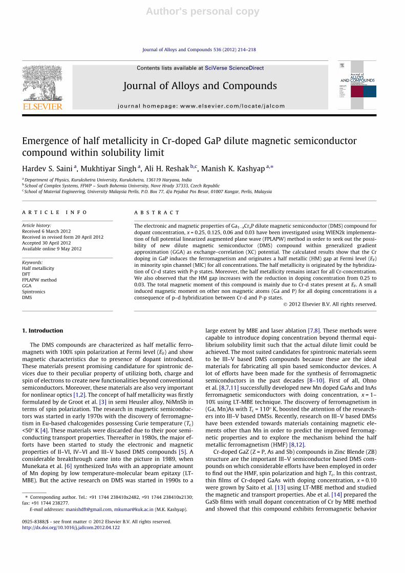
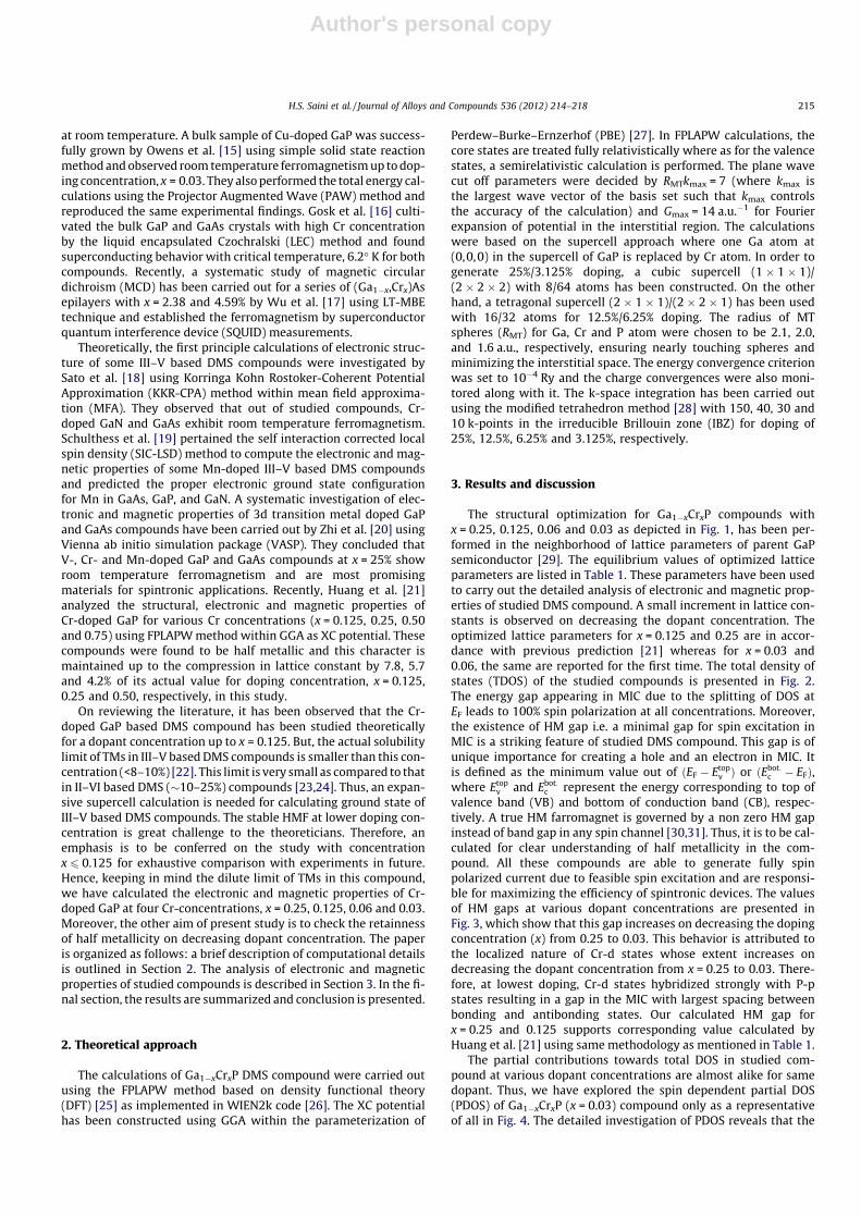
The structural optimization for Ga1�xCrxP compounds withx = 0.25, 0.125, 0.06 and 0.03 as depicted in Fig. 1, has been per-formed in the neighborhood of lattice parameters of parent GaPsemiconductor [29]. The equilibrium values of optimized latticeparameters are listed in Table 1. These parameters have been usedto carry out the detailed analysis of electronic and magnetic prop-erties of studied DMS compound. A small increment in lattice con-stants is observed on decreasing the dopant concentration. Theoptimized lattice parameters for x = 0.125 and 0.25 are in accor-dance with previous prediction [21] whereas for x = 0.03 and0.06, the same are reported for the first time. The total density ofstates (TDOS) of the studied compounds is presented in Fig. 2.The energy gap appearing in MIC due to the splitting of DOS atEF leads to 100% spin polarization at all concentrations. Moreover,the existence of HM gap i.e. a minimal gap for spin excitation inMIC is a striking feature of studied DMS compound. This gap is ofunique importance for creating a hole and an electron in MIC. Itis defined as the minimum value out of ðEF � Etop
v Þ or ðEbot:c � EFÞ,
where Etopv and Ebot:
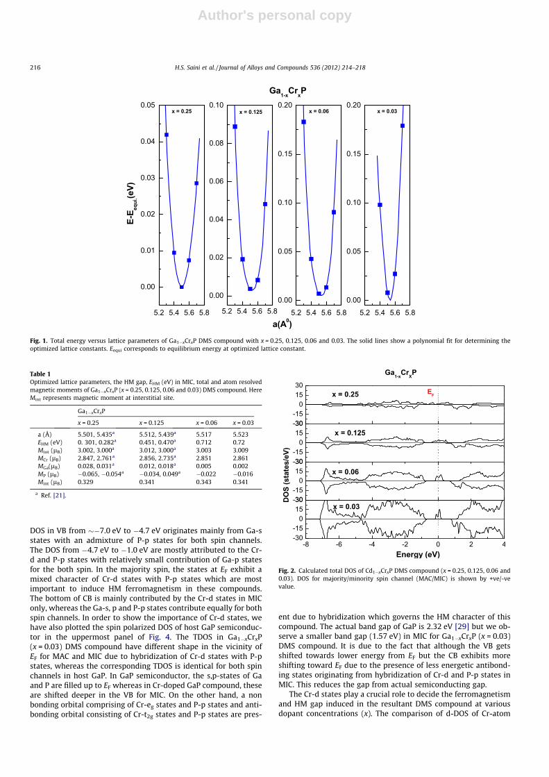
c represent the energy corresponding to top ofvalence band (VB) and bottom of conduction band (CB), respec-tively. A true HM farromagnet is governed by a non zero HM gapinstead of band gap in any spin channel [30,31]. Thus, it is to be cal-culated for clear understanding of half metallicity in the com-pound. All these compounds are able to generate fully spinpolarized current due to feasible spin excitation and are responsi-ble for maximizing the efficiency of spintronic devices. The valuesof HM gaps at various dopant concentrations are presented inFig. 3, which show that this gap increases on decreasing the dopingconcentration (x) from 0.25 to 0.03. This behavior is attributed tothe localized nature of Cr-d states whose extent increases ondecreasing the dopant concentration from x = 0.25 to 0.03. There-fore, at lowest doping, Cr-d states hybridized strongly with P-pstates resulting in a gap in the MIC with largest spacing betweenbonding and antibonding states. Our calculated HM gap forx = 0.25 and 0.125 supports corresponding value calculated byHuang et al. [21] using same methodology as mentioned in Table 1.
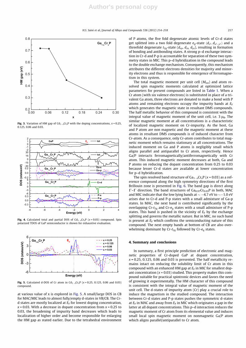
The partial contributions towards total DOS in studied com-pound at various dopant concentrations are almost alike for samedopant. Thus, we have explored the spin dependent partial DOS(PDOS) of Ga1�xCrxP (x = 0.03) compound only as a representativeof all in Fig. 4. The detailed investigation of PDOS reveals that the
H.S. Saini et al. / Journal of Alloys and Compounds 536 (2012) 214–218 215
Author's personal copy
DOS in VB from ��7.0 eV to �4.7 eV originates mainly from Ga-sstates with an admixture of P-p states for both spin channels.The DOS from �4.7 eV to �1.0 eV are mostly attributed to the Cr-d and P-p states with relatively small contribution of Ga-p statesfor the both spin. In the majority spin, the states at EF exhibit amixed character of Cr-d states with P-p states which are mostimportant to induce HM ferromagnetism in these compounds.The bottom of CB is mainly contributed by the Cr-d states in MIConly, whereas the Ga-s, p and P-p states contribute equally for bothspin channels. In order to show the importance of Cr-d states, wehave also plotted the spin polarized DOS of host GaP semiconduc-tor in the uppermost panel of Fig. 4. The TDOS in Ga1�xCrxP(x = 0.03) DMS compound have different shape in the vicinity ofEF for MAC and MIC due to hybridization of Cr-d states with P-pstates, whereas the corresponding TDOS is identical for both spinchannels in host GaP. In GaP semiconductor, the s,p-states of Gaand P are filled up to EF whereas in Cr-doped GaP compound, theseare shifted deeper in the VB for MIC. On the other hand, a nonbonding orbital comprising of Cr-eg states and P-p states and anti-bonding orbital consisting of Cr-t2g states and P-p states are pres-
ent due to hybridization which governs the HM character of thiscompound. The actual band gap of GaP is 2.32 eV [29] but we ob-serve a smaller band gap (1.57 eV) in MIC for Ga1�xCrxP (x = 0.03)DMS compound. It is due to the fact that although the VB getsshifted towards lower energy from EF but the CB exhibits moreshifting toward EF due to the presence of less energetic antibond-ing states originating from hybridization of Cr-d and P-p states inMIC. This reduces the gap from actual semiconducting gap.
The Cr-d states play a crucial role to decide the ferromagnetismand HM gap induced in the resultant DMS compound at variousdopant concentrations (x). The comparison of d-DOS of Cr-atom
Fig. 1. Total energy versus lattice parameters of Ga1�xCrxP DMS compound with x = 0.25, 0.125, 0.06 and 0.03. The solid lines show a polynomial fit for determining theoptimized lattice constants. Eequi corresponds to equilibrium energy at optimized lattice constant.
Table 1Optimized lattice parameters, the HM gap, EHM (eV) in MIC, total and atom resolvedmagnetic moments of Ga1�xCrxP (x = 0.25, 0.125, 0.06 and 0.03) DMS compound. HereMint represents magnetic moment at interstitial site.
Ga1�xCrxP
x = 0.25 x = 0.125 x = 0.06 x = 0.03
a (Å) 5.501, 5.435a 5.512, 5.439a 5.517 5.523EHM (eV) 0. 301, 0.282a 0.451, 0.470a 0.712 0.72Mtot (lB) 3.002, 3.000a 3.012, 3.000a 3.003 3.009MCr (lB) 2.847, 2.761a 2.856, 2.735a 2.851 2.861MGa(lB) 0.028, 0.031a 0.012, 0.018a 0.005 0.002MP (lB) �0.065, �0.054a �0.034, 0.049a �0.022 �0.016Mint (lB) 0.329 0.341 0.343 0.341
a Ref. [21].
Fig. 2. Calculated total DOS of Cd1�xCrxP DMS compound (x = 0.25, 0.125, 0.06 and0.03). DOS for majority/minority spin channel (MAC/MIC) is shown by +ve/-vevalue.
216 H.S. Saini et al. / Journal of Alloys and Compounds 536 (2012) 214–218
Author's personal copy
at various value of x is explored in Fig. 5. A small/large DOS in CBfor MAC/MIC leads to almost fully/empty d-states in VB/CB. The Cr-d states are mostly localized at EF for lowest doping concentration,x = 0.03. With a decrease in dopant concentration from x = 0.25 to0.03, the broadening of impurity band decreases which leads tolocalization of higher order and become responsible for enlargingthe HM gap as stated earlier. Due to the tetrahedral environment
of P atoms, the five fold degenerate atomic levels of Cr-d statesget splitted into a two fold degenerate eg-state ðdz2 ; dx2�y2 Þ and athreefold degenerate t2g-state (dxy, dzx, dyz), resulting in formationof bonding and antibonding states. A strong p–d exchange interac-tion in Cr-d and P-p is accountable for separation of these two sym-metry states in MIC. This p–d hybridization in the compound leadsto the double exchange mechanism. Consequently, this mechanismattributes the different electrons densities for majority and minor-ity electrons and thus is responsible for emergence of ferromagne-tism in this system.
The total magnetic moment per unit cell (Mtot) and atom re-solved spin magnetic moments calculated at optimized latticeparameters for present compounds are listed in Table 1. When aCr atom (with six valence electrons) is substituted in place of a tri-valent Ga atom, three electrons are donated to make a bond with Patoms and remaining electrons occupy the impurity bands at EF
which generates the magnetic state in resultant DMS compounds.The half metallic behavior of this compound is consistent with theintegral value of magnetic moment of the unit cell, i.e. 3 lB. Thesimilar magnetic moment at all concentrations is a characteristicof localized magnetic moment on Cr-impurity. As the host, Gaand P atom are non magnetic and the magnetic moment at theseatoms in resultant DMS compounds is of induced character fromCr-atom. As a consequence, only Cr-atom contributes to total mag-netic moment which remains stationary at all concentrations. Theinduced moment on Ga and P atoms is negligibly small whichaligns parallel and antiparallel to Cr atom, respectively. HenceGa/P interacts ferromagnetically/antiferromagnetically with Cratom. This induced magnetic moment decreases at both, Ga andP atoms on reducing the dopant concentration from 0.25 to 0.03because lesser Cr-d states are available at lower concentrationfor p–d hybridization.
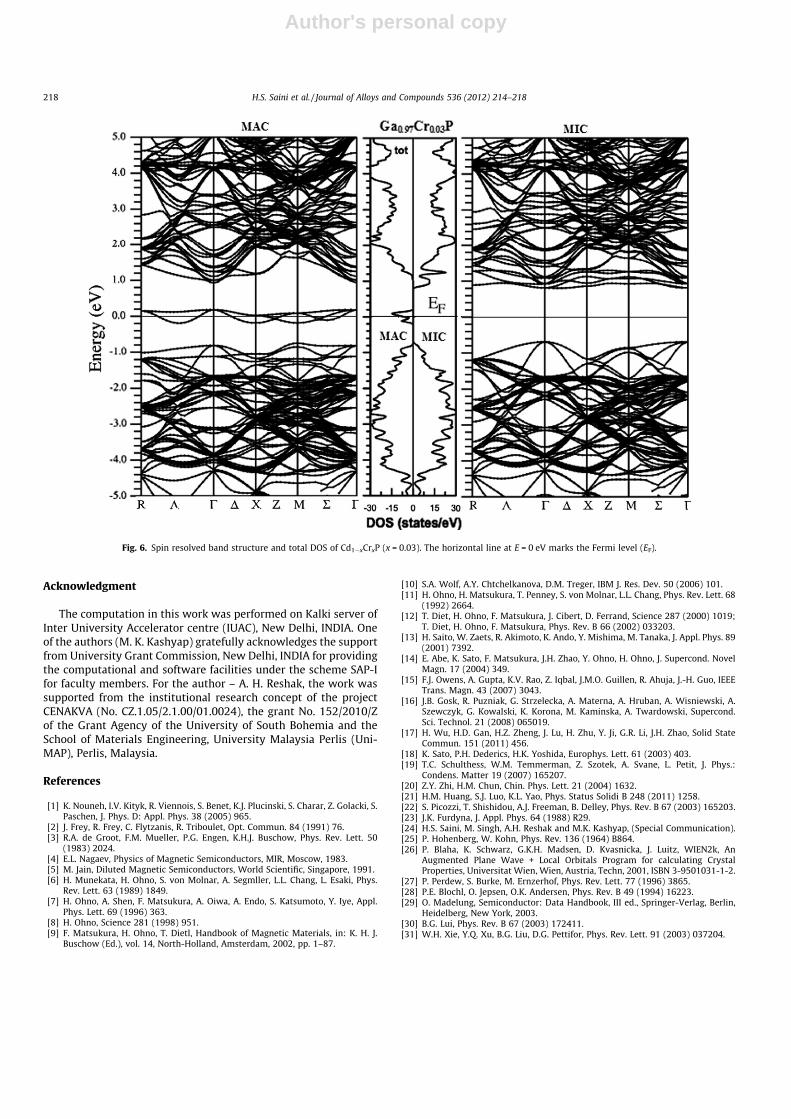
The spin resolved band structure of Ga1�xCrxP (x = 0.03) as a ref-erence compound along the high symmetry directions of the firstBrillouin zone is presented in Fig. 6. The band gap is direct alongC–C direction. The band structures of Ga0.97Cr0.03P in both, MACand MIC indicate that the low lying bands at��4.7 eV to��1.0 eVarises due to Cr-d and P-p states with a small admixture of Ga-pstates. In MAC, the next band is contributed significantly by theoverlapping Cr-t2g and Cr-eg states with a small admixture of P-pstates. This band is pushed in the vicinity of EF by the exchangesplitting and governs the metallic nature. But in MIC, no such bandis present at EF which confirms the semiconducting nature of thiscompound. The next empty bands at bottom of CB are also over-whelming dominant by Cr-t2g followed by Cr-eg states.
4. Summary and conclusions
In summary, a first principle prediction of electronic and mag-netic properties of Cr-doped GaP at dopant concentration,x = 0.25, 0.125, 0.06 and 0.03 is presented. The half metallicity re-mains intact on reducing the solubility limit of Cr atom in thiscompound with an enhanced HM gap at EF in MIC for smallest dop-ant concentration (x = 0.03) studied. This property makes this com-pound suitable for practical spintronic devices and favors the needof growing it experimentally. The HM character of this compoundis consistent with the integral value of magnetic moment of theunit cell. The d-states of impurity atom (Cr) play a crucial role toinduce the magnetism in the studied compound. The interactionbetween Cr-d states and P-p states pushes the symmetric d-statesat EF in MAC and away from EF in MIC which originates a gap in thelatter at all dopant concentrations. This p–d interaction reduces themagnetic moment of Cr atom from its elemental value and inducessmall local spin magnetic moment on nonmagnetic Ga/P atomwhich aligns parallel/antiparallel to Cr atom.
Fig. 3. Variation of HM gap of Cd1�xCrxP with the doping concentrations, x = 0.25,0.125, 0.06 and 0.03.
Fig. 4. Calculated total and partial DOS of Cd1�xCrxP (x = 0.03) compound. Spinpolarized TDOS of GaP semiconductor is shown for exhaustive evaluation.
Fig. 5. Calculated d-DOS of Cr atom in Cd1�xCrxP (x = 0.25, 0.125, 0.06 and 0.03)compound.
H.S. Saini et al. / Journal of Alloys and Compounds 536 (2012) 214–218 217
Author's personal copy
Acknowledgment
The computation in this work was performed on Kalki server ofInter University Accelerator centre (IUAC), New Delhi, INDIA. Oneof the authors (M. K. Kashyap) gratefully acknowledges the supportfrom University Grant Commission, New Delhi, INDIA for providingthe computational and software facilities under the scheme SAP-Ifor faculty members. For the author – A. H. Reshak, the work wassupported from the institutional research concept of the projectCENAKVA (No. CZ.1.05/2.1.00/01.0024), the grant No. 152/2010/Zof the Grant Agency of the University of South Bohemia and theSchool of Materials Engineering, University Malaysia Perlis (Uni-MAP), Perlis, Malaysia.
References
[1] K. Nouneh, I.V. Kityk, R. Viennois, S. Benet, K.J. Plucinski, S. Charar, Z. Golacki, S.Paschen, J. Phys. D: Appl. Phys. 38 (2005) 965.
[2] J. Frey, R. Frey, C. Flytzanis, R. Triboulet, Opt. Commun. 84 (1991) 76.[3] R.A. de Groot, F.M. Mueller, P.G. Engen, K.H.J. Buschow, Phys. Rev. Lett. 50
(1983) 2024.[4] E.L. Nagaev, Physics of Magnetic Semiconductors, MIR, Moscow, 1983.[5] M. Jain, Diluted Magnetic Semiconductors, World Scientific, Singapore, 1991.[6] H. Munekata, H. Ohno, S. von Molnar, A. Segmller, L.L. Chang, L. Esaki, Phys.
Rev. Lett. 63 (1989) 1849.[7] H. Ohno, A. Shen, F. Matsukura, A. Oiwa, A. Endo, S. Katsumoto, Y. Iye, Appl.
Phys. Lett. 69 (1996) 363.[8] H. Ohno, Science 281 (1998) 951.[9] F. Matsukura, H. Ohno, T. Dietl, Handbook of Magnetic Materials, in: K. H. J.
Buschow (Ed.), vol. 14, North-Holland, Amsterdam, 2002, pp. 1–87.
[10] S.A. Wolf, A.Y. Chtchelkanova, D.M. Treger, IBM J. Res. Dev. 50 (2006) 101.[11] H. Ohno, H. Matsukura, T. Penney, S. von Molnar, L.L. Chang, Phys. Rev. Lett. 68
(1992) 2664.[12] T. Diet, H. Ohno, F. Matsukura, J. Cibert, D. Ferrand, Science 287 (2000) 1019;
T. Diet, H. Ohno, F. Matsukura, Phys. Rev. B 66 (2002) 033203.[13] H. Saito, W. Zaets, R. Akimoto, K. Ando, Y. Mishima, M. Tanaka, J. Appl. Phys. 89
(2001) 7392.[14] E. Abe, K. Sato, F. Matsukura, J.H. Zhao, Y. Ohno, H. Ohno, J. Supercond. Novel
Magn. 17 (2004) 349.[15] F.J. Owens, A. Gupta, K.V. Rao, Z. Iqbal, J.M.O. Guillen, R. Ahuja, J.-H. Guo, IEEE
Trans. Magn. 43 (2007) 3043.[16] J.B. Gosk, R. Puzniak, G. Strzelecka, A. Materna, A. Hruban, A. Wisniewski, A.
Szewczyk, G. Kowalski, K. Korona, M. Kaminska, A. Twardowski, Supercond.Sci. Technol. 21 (2008) 065019.
[17] H. Wu, H.D. Gan, H.Z. Zheng, J. Lu, H. Zhu, Y. Ji, G.R. Li, J.H. Zhao, Solid StateCommun. 151 (2011) 456.
[18] K. Sato, P.H. Dederics, H.K. Yoshida, Europhys. Lett. 61 (2003) 403.[19] T.C. Schulthess, W.M. Temmerman, Z. Szotek, A. Svane, L. Petit, J. Phys.:
Condens. Matter 19 (2007) 165207.[20] Z.Y. Zhi, H.M. Chun, Chin. Phys. Lett. 21 (2004) 1632.[21] H.M. Huang, S.J. Luo, K.L. Yao, Phys. Status Solidi B 248 (2011) 1258.[22] S. Picozzi, T. Shishidou, A.J. Freeman, B. Delley, Phys. Rev. B 67 (2003) 165203.[23] J.K. Furdyna, J. Appl. Phys. 64 (1988) R29.[24] H.S. Saini, M. Singh, A.H. Reshak and M.K. Kashyap, (Special Communication).[25] P. Hohenberg, W. Kohn, Phys. Rev. 136 (1964) B864.[26] P. Blaha, K. Schwarz, G.K.H. Madsen, D. Kvasnicka, J. Luitz, WIEN2k, An
Augmented Plane Wave + Local Orbitals Program for calculating CrystalProperties, Universitat Wien, Wien, Austria, Techn, 2001, ISBN 3-9501031-1-2.
[27] P. Perdew, S. Burke, M. Ernzerhof, Phys. Rev. Lett. 77 (1996) 3865.[28] P.E. Blochl, O. Jepsen, O.K. Andersen, Phys. Rev. B 49 (1994) 16223.[29] O. Madelung, Semiconductor: Data Handbook, III ed., Springer-Verlag, Berlin,
Heidelberg, New York, 2003.[30] B.G. Lui, Phys. Rev. B 67 (2003) 172411.[31] W.H. Xie, Y.Q. Xu, B.G. Liu, D.G. Pettifor, Phys. Rev. Lett. 91 (2003) 037204.
Fig. 6. Spin resolved band structure and total DOS of Cd1�xCrxP (x = 0.03). The horizontal line at E = 0 eV marks the Fermi level (EF).
218 H.S. Saini et al. / Journal of Alloys and Compounds 536 (2012) 214–218
Copyright © 2022 FDOKUMEN