OUTLINE • Basic Semiconductor Physics (cont'd)
28
EE105 Spring 2008 Lecture 2, Slide 1 Prof. Wu, UC Berkeley Lecture 2 OUTLINE • Basic Semiconductor Physics (cont’d) – Carrier drift and diffusion • PN Junction Diodes – Electrostatics – Capacitance Reading: Chapter 2.1‐2.2 Lecture 1, Slide 1
-
Upload
khangminh22 -
Category
Documents
-
view
9 -
download
0
Transcript of OUTLINE • Basic Semiconductor Physics (cont'd)

EE105 Spring 2008 Lecture 2, Slide 1 Prof. Wu, UC Berkeley
Lecture 2
OUTLINE
• Basic Semiconductor Physics (cont’d)– Carrier drift and diffusion
• PN Junction Diodes– Electrostatics– Capacitance
Reading: Chapter 2.1‐2.2
Lecture 1, Slide 1
EE105 Spring 2008 Lecture 2, Slide 2 Prof. Wu, UC Berkeley
Dopant Compensation
• An N‐type semiconductor can be converted into P‐type material by counter‐doping it with acceptors such that NA > ND.
• A compensated semiconductor material has both acceptors and donors.
P‐type material(NA > ND)
DA
i
DA
NNnn
NNp
−≈
−≈2
AD
i
AD
NNnp
NNn
−≈
−≈2
N‐type material(ND > NA)

EE105 Spring 2008 Lecture 2, Slide 3 Prof. Wu, UC Berkeley
Types of Charge in a Semiconductor
• Negative charges:– Conduction electrons (density = n)
– Ionized acceptor atoms (density = NA)
• Positive charges:– Holes (density = p)
– Ionized donor atoms (density = ND)
• The net charge density (C/cm3) in a semiconductor is
( ) AD NNnpq −+−=ρ

EE105 Spring 2008 Lecture 2, Slide 4 Prof. Wu, UC Berkeley
Carrier Drift
• The process in which charged particles move because of an electric field is called drift.
• Charged particles within a semiconductor move with an average velocity proportional to the electric field.– The proportionality constant is the carrier mobility.
→→
→→
−=
=
Ev
Ev
ne
ph
μ
μ
Notation:μp ≡ hole mobility (cm2/V∙s)μn ≡ electron mobility (cm2/V∙s)
Hole velocity
Electron velocity
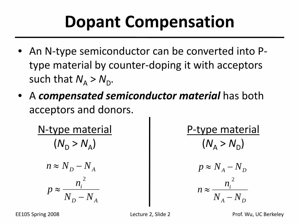
EE105 Spring 2008 Lecture 2, Slide 5 Prof. Wu, UC Berkeley
Velocity Saturation• In reality, carrier velocities saturate at an upper limit, called the saturation velocity (vsat).
E
vEv
bv
bE
sat
sat
0
0
0
0
1
1
μμ
μ
μμ
+=
=
+=
410 V/cmsatE ≈

EE105 Spring 2008 Lecture 2, Slide 6 Prof. Wu, UC Berkeley
Drift Current• Drift current is proportional to the carrier velocity and carrier concentration:
vh t A = volume from which all holes cross plane in time t
p vh t A = # of holes crossing plane in time t
q p vh t A = charge crossing plane in time t
q p vh A = charge crossing plane per unit time = hole current
Hole current per unit area (i.e. current density) Jp,drift = q p vh

EE105 Spring 2008 Lecture 2, Slide 7 Prof. Wu, UC Berkeley
Conductivity and Resistivity
• In a semiconductor, both electrons and holes conduct current:
• Conductivity
• Resistivity
• Typical resistivity range for Si: 10‐3 ~ 103 Ω‐cm
EEnpqJ
EqnEqpJJJ
EqnJEqpJ
npdrifttot
npdriftndriftpdrifttot
ndriftnpdriftp
σμμ
μμ
μμ
≡+=
+=+=
−−==
)(
)(
,
,,,
,,
[unit: mho/cm = S/cm]p nqp qnσ μ μ≡ +
1 [Unit: -cm]ρσ
≡ Ω

EE105 Spring 2008 Lecture 2, Slide 8 Prof. Wu, UC Berkeley
Resistivity Example• Estimate the resistivity of a Si sample doped with phosphorus
to a concentration of 1015 cm‐3 and boron to a concentration of 1017 cm‐3. The electron mobility and hole mobility are 800 cm2/Vs and 300 cm2/Vs, respectively.
EE105 Spring 2008 Lecture 2, Slide 9 Prof. Wu, UC Berkeley
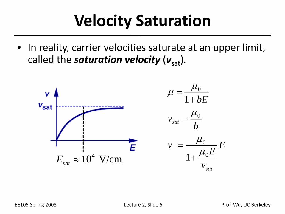
Electrical Resistance
where ρ is the resistivity
ResistanceWtL
IVR ρ=≡ (Unit: ohms)
V+ _
L
tW
I
homogeneously doped sample
EE105 Spring 2008 Lecture 2, Slide 10 Prof. Wu, UC Berkeley
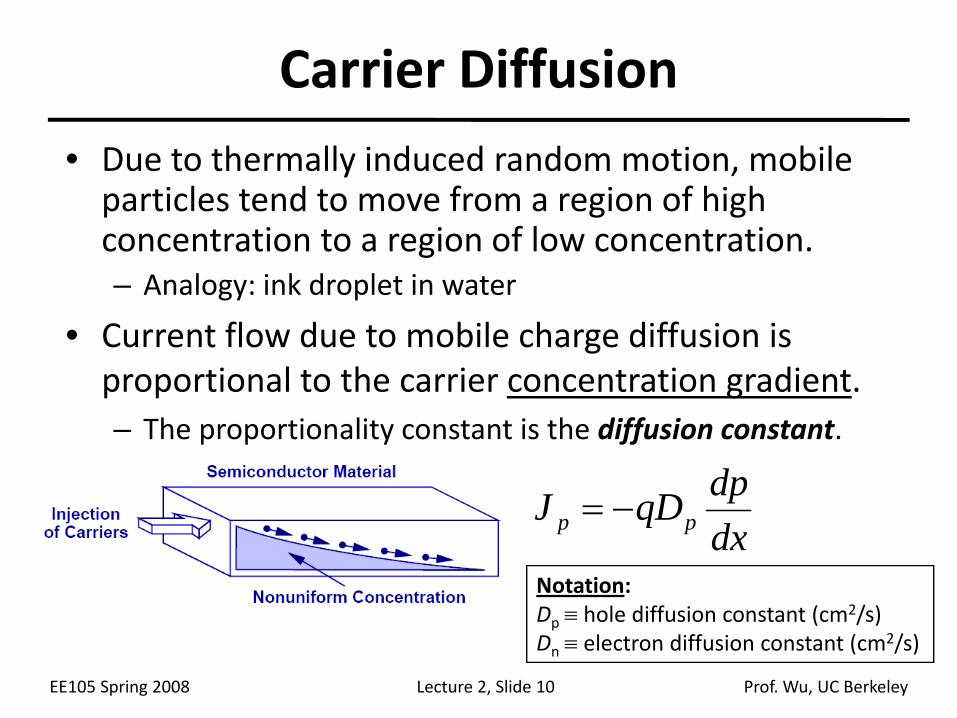
Carrier Diffusion• Due to thermally induced random motion, mobile particles tend to move from a region of high concentration to a region of low concentration. – Analogy: ink droplet in water
• Current flow due to mobile charge diffusion is proportional to the carrier concentration gradient.– The proportionality constant is the diffusion constant.
dxdpqDJ pp −=
Notation:Dp ≡ hole diffusion constant (cm2/s)Dn ≡ electron diffusion constant (cm2/s)

EE105 Spring 2008 Lecture 2, Slide 11 Prof. Wu, UC Berkeley
Diffusion Examples
• Non-linear concentration profile varying diffusion current
LNqD
dxdpqDJ
p
pdiffp
=
−=
,
dd
p
pdiffp
Lx
LNqD
dxdpqDJ
−=
−=
exp
,
• Linear concentration profileconstant diffusion current
dLxNp −
= exp⎟⎠⎞
⎜⎝⎛ −=
LxNp 1

EE105 Spring 2008 Lecture 2, Slide 12 Prof. Wu, UC Berkeley
Diffusion Current
• Diffusion current within a semiconductor consists of hole and electron components:
• The total current flowing in a semiconductor is the sum of drift current and diffusion current:
)(
,
,,
dxdpD
dxdnDqJ
dxdnqDJ
dxdpqDJ
pndifftot
ndiffnpdiffp
−=
=−=
diffndiffpdriftndriftptot JJJJJ ,,,, +++=

EE105 Spring 2008 Lecture 2, Slide 13 Prof. Wu, UC Berkeley
The Einstein Relation
• The characteristic constants for drift and diffusion are related:
• Note that at room temperature (300K)– This is often referred to as the “thermal voltage”.
q
kTD=
μ
mV26≅q
kT

EE105 Spring 2008 Lecture 2, Slide 14 Prof. Wu, UC Berkeley
The PN Junction Diode
• When a P‐type semiconductor region and an N‐type semiconductor region are in contact, a PN junction diode is formed. VD
ID
+–

EE105 Spring 2008 Lecture 2, Slide 15 Prof. Wu, UC Berkeley
Diode Operating Regions
• In order to understand the operation of a diode, it is necessary to study its behavior in three operation regions: equilibrium, reverse bias, and forward bias.
VD = 0 VD > 0VD < 0

EE105 Spring 2008 Lecture 2, Slide 16 Prof. Wu, UC Berkeley
Carrier Diffusion across the Junction• Because of the difference in hole and electron concentrations on each side of the junction, carriers diffuse across the junction:
Notation:nn ≡ electron concentration on N‐type side (cm‐3)pn ≡ hole concentration on N‐type side (cm‐3)pp ≡ hole concentration on P‐type side (cm‐3)np ≡ electron concentration on P‐type side (cm‐3)

EE105 Spring 2008 Lecture 2, Slide 17 Prof. Wu, UC Berkeley
Depletion Region• As conduction electrons and holes diffuse across the junction, they leave behind ionized dopants. Thus, a region that is depleted of mobile carriers is formed.– The charge density in the depletion region is not zero.
– The carriers which diffuse across the junction recombine with majority carriers, i.e. they are annihilated.
width=Wdep
quasi-neutral region
quasi-neutral region

EE105 Spring 2008 Lecture 2, Slide 18 Prof. Wu, UC Berkeley
The Depletion ApproximationIn the depletion region on the N side:
( )bxqNE
qNdxdE
si
D
si
D
si
+=
==
ε
εερ
ρ(x)
x-qNA
qND
In the depletion region on the P side:
( )xaqNE
qNdxdE
si
A
si
A
si
−=
−==
ε
εερ
DA bNaN =
a-b
1210 F/cmsiε =
Gauss’s Law

EE105 Spring 2008 Lecture 2, Slide 19 Prof. Wu, UC Berkeley
Potential Distribution
• In the depletion region, the electric potential is quadratic since the electric field is linear
• The potential difference between the N and the P side is called built‐in potential, V0
V(x)
xa-b
V0
0
dVEdx
V E dx
= −
= − ⋅∫

EE105 Spring 2008 Lecture 2, Slide 20 Prof. Wu, UC Berkeley
PN Junction in Equilibrium
• In equilibrium, the drift and diffusion components of current are balanced; therefore the net current flowing across the junction is zero.
diffndriftn
diffpdriftp
JJ
JJ
,,
,,
−=
−=
0,,,, =+++= diffndiffpdriftndriftptot JJJJJ

EE105 Spring 2008 Lecture 2, Slide 21 Prof. Wu, UC Berkeley
Built‐in Potential, V0
• Because of the electric field in the depletion region, there exists a potential drop across the junction:
( )2
( ) ( ) ln ln/
p
n
p p p p
pa
p pb p
p p A
p n i D
dp dV dpqp E qD p Ddx dx dx
dpdV Dp
D p NkTV b V ap q n N
μ μ
μ
μ
−
⎛ ⎞= ⇒ − =⎜ ⎟⎝ ⎠
⇒ − =
⇒ − − = =
∫ ∫
ln 20i
DA
nNN
qkTV = (Unit: Volts)
b− a

EE105 Spring 2008 Lecture 2, Slide 22 Prof. Wu, UC Berkeley
Built‐In Potential Example
• Estimate the built‐in potential for PN junction below.
N P
ND = 1018 cm-3 NA = 1015 cm-3
( ) ( ) ( )18 15
130 2 20
0
10 10ln 26mV ln 26mV ln 1010
Note: ln(10) 26mV 2.3 60mV
60mV 13 780mV
D A
i
N NkTVq nkTq
V
⎛ ⎞ ⎛ ⎞= = =⎜ ⎟ ⎜ ⎟
⎝ ⎠⎝ ⎠
≅ × ≅
= × =

EE105 Spring 2008 Lecture 2, Slide 23 Prof. Wu, UC Berkeley
PN Junction under Reverse Bias • A reverse bias increases the potential drop across the junction. As a result, the magnitude of the electric field increases and the width of the depletion region widens.
( ) 112 0 RDA
sidep VV
NNqW +⎟⎟
⎠
⎞⎜⎜⎝
⎛+=
ε

EE105 Spring 2008 Lecture 2, Slide 24 Prof. Wu, UC Berkeley
Diode Current under Reverse Bias• In equilibrium, the built‐in potential effectively prevents carriers from diffusing across the junction.
• Under reverse bias, the potential drop across the junction increases; therefore, negligible diffusion current flows. A very small drift current flows, limited by the rate at which minority carriers diffuse from the quasi‐neutral regions into the depletion region.

EE105 Spring 2008 Lecture 2, Slide 25 Prof. Wu, UC Berkeley
PN Junction Capacitance• A reverse‐biased PN junction can be viewed as a capacitor. The depletion width (Wdep) and hence the junction capacitance (Cj) varies with VR.
2
[F/cm ]
sij
dep
CWε
=

EE105 Spring 2008 Lecture 2, Slide 26 Prof. Wu, UC Berkeley
Voltage‐Dependent Capacitance
εsi ≅ 10‐12 F/cm is the permittivity of silicon
00
0
0
12
1
VNNNNqC
VV
CC
DA
DAsij
R
jj
+=
+=
εVD

EE105 Spring 2008 Lecture 2, Slide 27 Prof. Wu, UC Berkeley
Reverse‐Biased Diode Application
• A very important application of a reverse‐biased PN junction is in a voltage controlled oscillator (VCO), which uses an LC tank. By changing VR, we can change C, which changes the oscillation frequency.
LCfres
121π
=

EE105 Spring 2008 Lecture 2, Slide 28 Prof. Wu, UC Berkeley
Summary• Current flowing in a semiconductor is comprised of drift and diffusion components:
• A region depleted of mobile charge exists at the junction between P‐type and N‐type materials.– A built‐in potential drop (V0) across this region is established by the charge density profile; it opposes diffusion of carriers across the junction. A reverse bias voltage serves to enhance the potential drop across the depletion region, resulting in very little (drift) current flowing across the junction.
– The width of the depletion region (Wdep) is a function of the bias voltage (VD).
dxdpqD
dxdnqDEqnEqpJ pnnptot −++= μμ
ln 20i
DA
nNN
qkTV =( ) 112 0 D
DA
sidep VV
NNqW −⎟⎟
⎠
⎞⎜⎜⎝
⎛+=
ε