Japanese semiconductor industry service - Computer History ...
540
News l e t ters 1983-1984 "" zs 'J««5\ Japanese Semiconductor Industry Service 1290 Ki dder Park Dri ve San Jose, Cal i f ornia 95131 (408) 971-9000 Telex: 171973 Sales/ Service offices: UNITED K I NGD O M GERMANY DATAQUEST UK Limited DATAQUEST GmbH 144/146 New Bond Street In der Schneithohl 17 London WIY 9FD D-6242 Kronberg 2 United Kingdom West Germany (01) 409-1427 (06173) 6921 Telex: 266195 Telex: 410939 FRANCE JAPAN ' DATAQUEST SARL DATAQUEST Japan, Ltd. 41, rue Ybry Azabu Heights, Suite 711 92522 Neuilly-sur-Seine Cedex 1-5-10, Roppongi, Minato-ku France Tokyo 106, Japan (01) 758-1240 (03) 582-1441 Telex: 630842 Telex: J32768 The content of this report represents our interpretation and analysis of infor- mation generally available to the public or released by responsible individuals in the subject companies, but is not guaranteed as to accuracy or completeness. It does not contain material provided to us in confidence by our clients. This information is not furnished in connection with a sale or offer to sell securities, or in connection with the solicitation of an offer to buy securities. This firm and its parent and/or their officers, stockholders, or members of their families may, from time to time, have a long or short position in the securities mentioned and may sell or buy such securities. Printed in the United States of America. All rights reserved. No part of this publication may be reproduced, stored in retrieval systems, or transmitted, in any form or by any means—mechanical, electronic, photocopying, duplicating, microfilming, videotape, or otherwise—without the prior written permission of the publisher. © 1984 Dataquest Incorporated Also © 1983 Dataquest Incorporated
-
Upload
khangminh22 -
Category
Documents
-
view
3 -
download
0
Transcript of Japanese semiconductor industry service - Computer History ...

Newsletters 1983-1984
"" zs 'J««5\
Japanese Semiconductor Industry Service
1290 Kidder Park Drive San Jose, California 95131
(408) 971-9000 Telex: 171973
Sales/Service offices:
UNITED K I N G D O M GERMANY DATAQUEST UK Limited DATAQUEST GmbH 144/146 New Bond Street In der Schneithohl 17
London WIY 9FD D-6242 Kronberg 2 United Kingdom West Germany
(01) 409-1427 (06173) 6921 Telex: 266195 Telex: 410939
FRANCE JAPAN ' DATAQUEST SARL DATAQUEST Japan, Ltd.
41, rue Ybry Azabu Heights, Suite 711 92522 Neuilly-sur-Seine Cedex 1-5-10, Roppongi, Minato-ku
France Tokyo 106, Japan (01) 758-1240 (03) 582-1441 Telex: 630842 Telex: J32768
The content of this report represents our interpretation and analysis of information generally available to the public or released by responsible individuals in the subject companies, but is not guaranteed as to accuracy or completeness. It does not contain material provided to us in confidence by our clients.
This information is not furnished in connection with a sale or offer to sell securities, or in connection with the solicitation of an offer to buy securities. This firm and its parent and/or their officers, stockholders, or members of their families may, from time to time, have a long or short position in the securities mentioned and may sell or buy such securities.
Printed in the United States of America. All rights reserved. No part of this publication may be reproduced, stored in retrieval systems, or transmitted, in any form or by any means—mechanical, electronic, photocopying, duplicating, microfilming, videotape, or otherwise—without the prior written permission of the publisher.
© 1984 Dataquest Incorporated Also © 1983 Dataquest Incorporated


Dataqiicst RESEARCH BULLETIN
JSIS Code: Newsletters 1985-1986, EIEJ 1986-7
NEC INSTITUTES TOXIC WASTE SURVEY
SUMMARY
Due to growing concern over toxic wastes, Kyushu NEC recently announced a pollution prevention agreement with Kumamoto City and has implemented a study to investigate measures for preventing toxic waste problems. The basic agreement includes the following provisions:
• Basic understanding regarding pollution prevention
• Prior consultation with Kumamoto City before construction or changes in Kyushu NEC's manufacturing processes
• Urgent countermeasures
• Immediate study to investigate carcinogenic gases and chemicals
Kyushu NEC plans to issue a detailed agreement in June 1986 after investigating the mattei:. The agreement will cover the existing toxic waste situation, standards for individual gases and chemicals, monitoring systems, and closed water-recycling systems.
DATAQUEST ANALYSIS
DATAQUEST believes that Kyushu NEC's announcement is an indication of the serious concern over toxic wastes among Japanese semiconductor companies. Moreover, it is NEC's step to protect its plant on Kyushu island, Japan's "Silicon Island," where the company is producing 256K and 1Mb DRAMS.
During the last year, DATAQUEST has been visited by Japanese prefectural government officials who are clearly worried about toxic wastes and farmland preservation. Unlike Silicon Valley where IC plants are several miles from housing areas, most Japanese IC plants are located within several hundred yards of prime farmlands and housing areas. Given
© 1986 Dataquest Incorporated Jan. 22 ed.-Reproduction Prohibited
The content of this report represents our interpretation and analysis of mtormation generally available to the pubic or released tjy responsible individuals in the subject companies txjt is not guaranteed as to accuracy or completeness It does not contain
material provided to us m confidence by ouf clients Individual companies reported on and analyzed by WTAQUEST may be c'lerts of this and/or other DATAQUEST services This intormalion is not furnished m connection with a sale or offer to sell secuniies
or in connection with the sdtcilation o( an offer to buy securlies This firm and its parent and/or their officer stockholders or members ol thetr families may, from nme to time have a long or short position in the secunties mentioned and may sell or buy such securities
Dataquest Incorporated, 1290 Ridder Park Drive, San Jose, CA 95131-2398, (408) 971-9000, Telex 171973

Japan's frequent earthquakes, typhoons, and other natural disasters, toxic leaks could trigger a public outcry and seriously hamper Japanese semiconductor makers. According to the Japanese press, most prefectural governments lack toxic waste standards for high-tech industries. Japan's existing environmental regulations, a result of industrial poisoning cases in the mid-1970s, are aimed at heavy industries.
In an effort to protect the public and prevent this issue from becoming a political football, DATAQUEST believes that other Japanese semiconductor makers will also announce agreements with local governments in the future. We applaud NEC for taking the initiative in this difficult matter and believe that MITI and other semiconductor makers are closely examining the Semiconductor Industry Association (SIA) model toxic waste ordinance for possible implementation in Japan.
Sheridan Tatsuno
- 2 -

Dataquest JAPANESE RESEARCH NEWSLETTER
JSIS Code: EIEJ Newsletters
THE U.S. ECONOMY: BOOM OR BUST?
In a recent visit to DATAQUEST, Joseph W. Duncan, Corporate Economist and Chief Statistician of the Dun & Bradstreet Corporation, shared some of his views on the future of the U.S. economy. Due to the universal nature of the subject matter and the impressive credentials of Mr. Duncan, we believe that his views would be of interest to our clients. Mr. Duncan worked eight years as the chief statistician for the Office of Information and Regulatory Affairs of the U.S. Office of Management and Budget. Previously, he was a research and management specialist at Battelle Memorial Institute where he spent 13 years. Mr. Duncan's education includes receiving a B.S.M.E. degree from Case Institute of Technology, an M.B.A. degree from Harvard Graduate School of Business Administration, and a Ph.D. degree in Economics from Ohio State University. He also attended the London School of Economics.
KEY ECONOMIC ISSUES
With respect to the health of the U.S. economy, Mr. Duncan identified three key questions:
• Will there be a recession in the near future?
• Will activity continue in capital markets?
• Will Congress act to reduce the budget deficit?
Recession
In order to address the likelihood of a recession, one must address the health of principal components of the economy. These vital components are consumer spending—which makes up approximately two-thirds of the GNP—housing starts, business starts/failures, unemployment, capital spending, and inflation.
Consumer spending is expected to remain strong. Contrary to widely held beliefs, Mr. Duncan believes that consumers are not over-extended because monthly payments remain a small percentage of disposable income. The housing market appears to be garnering pent-up demand, as mortgage rates have remained at the pivotal 12 percent for some time now. Rates are expected to drift down below 12 percent, however, which should trigger a very strong housing market.
1985 Dataquest Incorporated Nov. 22-Reproduction Prohibited
The content of this report represents our interpretaion and anaIysis of information generaIly available to the public or released by responsible individuals in Ihe subject companies, but is not guaranteed as to accuracy or completeness It does not contain material provided to us in confidence by our clients Individual companies reported on and analyzed by DATAQUEST, may be clients of this and/or other DATAQUEST services This information is not furnished in connection with a sale or offer to sell securities or in connection with the solicitation of an offer to buy securities This firm and its parent and/or their officers, stockholders, or members of their families may, from time to time, have a Iong or short position in the securities mentioned and may seII or buy such securities.
Azabu Heights, Suite 711, 1-5-10 Roppongi, i\/linato-ku, Tokyo 106, Japan 1290 Ridder Park Drive / San Jose, CA 95131 / (408) 971-9000 / Telex 171973

1 Business starts are at an all-time high. This bears no correlation to interest
rates; rather, it is attributed to a more entrepreneurial spirit and willingness to take risks. While business starts are up, so too are business failures. There are several reasons for this: small businesses pay very high interest rates and are at high risk for failure. Also, liberalized personal bankruptcy laws have made it more acceptable to file bankruptcy claims.
Employment has grown continuously during the last five years. Import activity, which would seem to adversely affect the health of the economy, does, in fact, add jobs in the United States. Thus, import activity together with strengthened demand from overseas markets for U.S. exports, should be bolstered.
Capital Market Activity
Capital spending has been depressed due to uncertainty of its treatment under proposed tax reforms. Yet, Mr. Duncan believes that tax reform will not occur until 1987. Spending is expected to pick up in 1986, along with corporate profits. Corporate cash flow will be up 5 percent in 1985, while profits will be down 5 percent. Inflation will increase as well, but is not expected to exceed a 5 percent annual rate.
We believe that there are two sides to the U.S. economy: production, expressed as gross national product (GNP) and consumption, which we refer to as gross final domestic demand (GFDD). To get a good view of the economy, one should look at both. GFDD measures the strength of demand in the economy by factoring net exports and inventory change out of GNP: GFDD = GNP - change in inventory + imports - exports. As shown in Figure 1, the GFDD points to a healthy market with 3.3 percent growth between the fourth quarter of 1984 and the third quarter of 1985. Forecasts of real GNP identify growth of 2.7 percent for 1985, 3.5 percent for 1986, and 4.5 percent for 1987. Growth in GFDD is forecast to remain higher than GNP growth through the end of 1985.
Congressional Action
It is highly probable that the U.S. economy will not experience another recession until 1989. If Congress acts to pass a budget balancing bill, the economy should experience moderate growth for several years. However, if the deficit is not reduced, interest rates could start spiraling as early as spring of 1986, and a recession would soon follow. We believe Congress will act to balance the budget.
SUMMARY
Mr. Duncan identifies a healthy U.S. market. DATAQUEST concurs with his assessment and agrees that 1986 will be a healthy year. Our forecast for semiconductor growth assumes light growth in the first quarter of 1986 with more
1985 Dataquest Incorporated Nov. 22 JSIS Newsletter

robust growth in the latter quarters. Our long-range forecast also identifies a recessionary period in 1989. While it is not clear that the semiconductor market clearly follows the GNP, we believe that the overall economy sets the general trend for the health of our industry.
Patricia S. Cox Barbara A. Van
Figure 1
Real U.S. GNP Versus Real Gross Final Domestic Demand (Trillions of 1972 Dollars)
Quar ter /Year D Real GNP + Real GFD
Source: Wharton Econometric Forecasting Associates DATAQUEST
JSIS Newsletter 1985 Dataquest Incorporated Nov. 22

Dataquest RESEARCH BULLETIN
JSIS Code: EIEJ Newsletters
SEVENTH ANNUAL GaAs SYMPOSIUM NOVEMBER 12-14, 1985
Interest in gallium arsenide (GaAs) ICs has grown rapidly in recent years. Attendance at the lEEE-sponsored GaAs IC symposium has grown more than 30 percent annually since 1982, reaching 850 at this year's meeting in Monterey, California. Abstract submittals increased 24 percent over 1984, indicating substantial growth in development activity.
HIGHLIGHTS
General
Forty-nine papers, approximately evenly split among analog ICs, digital ICs, and technology topics
Authors from 26 companies, 5 universities, and 2 other organizations
Three panel discussions covering millimeter-wave ICs, LSI issues, foundry operations, and standardization
Key Papers
\
A GaAs, 12-bit, 1-GHz digital-to-analog converter (DAC)— Hewlett-Packard Labs
A 115-GHz, monolithic, GaAs, PET oscillator—Texas Instruments
r\r\ A 2 . 6 n s , t g g , IK^jj 4 SRAM us ing enhancement /dep le t ion MESPETs (two papers )—Hitacf i i
An ECL-compatible, IK SRAM ^ w i t t i \ s m a l l e s t c e l l r e p o r t e d t o da t e )—Texas In s t rumen t s
© 1985 Dataques t Inco rpora t ed Nov. 19 ed . -Reproduc t ion P r o h i b i t e d
Tne contenI o ' Ifiis reporl regresenl
provided 10 us n confidence b> our c
w , i M n e s „ i , r a a i , o . . o l a n o l i e , l < , O i
.ems
ysec
nierpreiai
Individual
uni ies Th
in and ana
companies
l inn and
,Si5 0l
reporied
soa.nn i
To rn anon
on and ana
and/o, ihei
gennia
, i e 0 0
iKI ice,
, a . a i i a l i n n
DATAQUEKT
s s.ookdoide
n, p,
n-.a,
, 0. n
III! or
e i i i e
nmlie
,eie
I S O
s o l
s e n
• m
, i n
, d ,
po-s.Ole indi. i
older DATAQ
i ra i s i n i nesub ieo
JEST services This
n e i o i i m e ha-e a
conip
inlorir
ng or
m e
alio
h o r
IJO
n i s n
p o s
i s n
01 rr
l ion
1 gua
imshe
n i ne
an ieedas loao
d i n c o n n e c l i o
secor i i iesmen
curacy or compielene,ss
wiih a sale or oiler lo sel
oned and may sell or Cuy
i d o e s n o i c
securiiies o
sucn secur
i m a m
in con
lies
Tialenal
necl ion
Dataquest Incorporated, A Subsidiary of A.C. Nielsen Company / 1290 Ridder Park Drive / San Jose, CA 95131 / (408) 971-9000 / Telex 171973

* A 400-MHz band prescaler (for hand-tield radio)—Toshiba
'—r • An 8 x^^8 multiplier (5.6ns at 1.45V) witti 20-bit accumu
lator—Sony
• A high-temperature (18 0 degrees C) GaAs hall-effect sensor— Siemens "$
OBSERVATIONS AND CONCLUSIONS
GaAs IC technology is extending semiconductors to new frontiers of speed, speed/power efficiency, temperature extremes, and radiation resistance. Analog GaAs ICs are already commercially viable, with free-world market shipments exceeding 350 million annually.
However, present merchant market activities in GaAs digital ICs are severely limited by quality of starting material, ttireshold control, lack of test equipment for use in a production environment, chip interface/ packaging standardization, and other restrictions. DATAQUEST believes that the 1985 GaAs digital IC market will be less than $15 million worldwide.
Explosive merchant market growth rates exceeding 100 percent a year for SRAMs, gate arrays, and other LSI devices are achievable as the restrictions mentioned above are resolved. At such time, demand will rapidly grow to more than $1 billion annually. The wafer-processing capacity required to support such a business level is quickly achievable, and the technical expertise is available, as demonstrated by this year's papers.
Gene Miles
- 2 -

Dataquest RESEARCH BULLETIN
JSIS Code: EIEJ Newsletters
JAPAN PLANS NEW MARKET-OPENING MEASURES
On September 4, Motoo Shiina, Vice Chairman of the Policy Research Commission for Japan's Liberal Democratic Party (LDP), met with members Of Stanford Iftiiversity's U.S.-Japan Porum to discuss trade friction issues. Mr. Shiina is a high-ranking LDP official responsible for drafting trade policies for Prime Minister Yasuhiro Nakasone. He is currently touring the United States to gather information and evaluate prevailing attitudes toward protectionism. Mr. Shiina made the following points during the discussion:
• Japanese export restraint may be necessary to defuse explosive trade friction, but it is only a short-term solution. Japanese market opening is the only long-term solution.
• MITI held a conference in June with 60 Japanese companies to request a $5 billion increase in purchases from the United States. These companies are already planning to purchase $2 billion in fiscal 1985, so an "affirmative action program" would only net about $3 billion. MITI is planning to call in another 73 companies to increase total purchases from the United States to $10 billion.
• Americans have requested that Japan implement policies to expand domestic demand, but Japan has limited policy options.
Lowering interest rates would weaken the yen further and increase Japanese exports to the United States, while raising interest rates would shut off domestic growth and reduce U.S. imports.
Increased public spending runs counter to the government's efforts to reduce its large budget deficits.
© 1985 Dataquest Incorporated Sept. 10 ed.-Reproduction Prohibited • «
Tne
prov
"""
come
, !edi
I h e ,
nl or Ihis repor
OS 10 coodoeo
(icitai ion of an
represent
e b y o u r c
oi ler ,0 00
our
ems
yser-
Ind i .n lua lcom
ml anal
laoies
and il
epor ieoon
niaiio
anoar
general
aiy?eclb
r o l l i c e ,
y ayailaOie ir, !n( p^o
OAIAQUEST may Pe
s siockPoiOers or me
( o r r e i e i . e
c i e n i s o r n
^ O e r s o i n e
l l , r e - p O r
1 . ,nO r o
. l „ n , l „ s
s ,P ie ,na . . ,Ooa is ,n ines „o ,e ,
her DATAQUEST servrces Th
,ay i r o m i r m c l o i . m e haye a
1 on.pa
inlorrn
o n g o . s
o e s
horl
Pu
IS
PO
S n
il ion
1 gr.aran
rnisheO
n i h e s e
e e r l a s m a
nconnec i io
urines men
curacy or compleleness n o
n Arih a sale or oiler lo sell se
i ioneo and may sell or buy s
curme
en sec
conlain
o r i n c o n
ool ies
oaleoai
oecl ion
Dataquest Incorporated, A Subsidiary of A.C. Nielsen Company / 1290 Bidder Park Drive / San Jose, CA 95131 / (408) 971-9000 / Telex 171973

- Private investment in the public sector is being pursued, but it is difficult to implement in practice.
- Re-regulation of Japanese capital outflows would bolster the yen and free up funds for domestic spending. A 2 percent to 3 percent tax on interest income earned abroad .might stem the current outflow.
Mr. Shiina said that Japanese officials are extremely worried about a protectionist backlash in the united States this year, which would seriously weaken the Japanese economy. Thus, MITI is asking Japanese companies to help defuse the trade friction by buying more abroad. Even the Ministry of Posts and Telecommunications, which has been very protectionist to date, is beginning to feel the heat.
DATAQUEST believes that Prime Minister Nakasone will make another market-opening announcement this fall based on Mr. Shiina's policy recommendations. This announcement will probably elaborate on his "affirmative action program" and possibly list the procurement plans announced by major Japanese companies. We note that Hitachi has already announced that it will spend $120 million by December 1986, while NEC will increase its purchases from $160 million to $200 million by 1987. Other major companies are expected to make their announcements this fall.
Sheridan Tatsuno
- 2 -

Dataquest JAPANESE RESEARCH NEWSLETTER
JSIS Code: EIEJ Newsletters
WORLDWIDE TECHNICAL MEETINGS
Because of the need to be aware of important bus iness / technica l meetings throughout the world, DATAQUEST has compiled a calendar covering major meetings of importance to a l l JSIS c l i e n t s .
We have researched and are now making ava i lab le to you a calendar for the period from September 1985 through June 1986. The calendar l i s t s meeting da t e s , t i t l e s , l oca t ions , and addresses for i n q u i r i e s .
Gene Norrett
© 1985 Dataquest Incorporated Sept. 4 ed.-Reproduction Prohibited
The content of this report represents our interpretaion and analysis of information generally available to the public or released by responsible individuals in the subject companies, but is not guaranteed as to accuracy or completeness. It does not contain material provided to us in confidence by our clients. Individual companies reported on and analyzed by DATAQUEST, may be clients of this and/or other DATAQUEST services This information is not furnished in connection with a sale or offer to sell securities or in connection with the solicitation of an offer to buy securities This firm and its parent andlor their officers, stockholders, or members of their families may, from time to time, have a long or short position in the securities mentioned and may sell or buy such securities.
Azabu Heights, Suite 711, 1-5-tO RoppongI, MInato-ku, Tokyo 106, Japan 1290 Bidder Park Drive / San Jose, CA 95131 / (408) 971-9000 / Telex 171973

JSIS ELECTRONICS CALENDAR
#
Date
9 / 3 - 6
9 / 4 - 1 1
9 / 9 - 1 2
9 / 9 - 1 2
9 / 9 - 1 2
9 / 9 - 1 2
9 / 9 - 1 3
9 / 1 0 - 1 3
flctivity
11 th Symposiuni on Microp r o c e s s i n g & Microp rogramming (EUROMICRO 85)
l l t n I n t e r n a t i o n a l T e l e -t r a f f i c Cong ress (ITC 11)
31s t N a t i o n a l Qsnfe rence on I n f o r m a t i o n P r o c e s s i n g
IStti European S o l i d S t a t e Dev ice Resea rch Con fe rence (ESSDERC '85)
IStti European Microwave Confe rence
IEEE I n t e r n a t i o n a l Q3mputer C o n f e r e n c e and E x h i b i t i o n (COMPINT 85)
l o c a t i o n
B r u s s e l s , Belgium
Koku r i t su Kyoto Kokusai Kaikan Taka raga lke , Sakyoku, Kyoto
Gakushuin Un iv . Kinen Kaikan Itostiiniaku, ISokyo ( S e p t . 9 on ly ) & Tokyo Denki Un iv . Kanda, Chiyoda-ku Tokyo
Aachen, F e d e r a l Republ i c o f Germany
P a l a i s d e s Congres P a r i s , F rance
M o n t r e a l , Quebec Canada
8th I n t e r n a t i o n a l Con f e rence Rome, I t a l y on N o i s e i n P h y s i c a l Systems 4th I n t e r n a t i o n a l Con f e ren ce on 1 / f Noise
9th Data Communications Symposium
W h i s t l e r Mountain B r i t i s h Columbia
I n q u i r i e s
Klaus Waldschmidt J.W. Q o e t h e - U n i v e r s i t a t F a c h b e r e i c h 2 0 , P .O. Box 11 19 3 2 , F rankfu r t F e d e r a l Republ i c o f Germany
Kokusai Ka ig i Jimukyoku Kasho B l d g , 2 - 1 4 - 9 Nihonbashi , Chuoku, Tokyo 103 (03) 272-8011
JDhoshor i C^kkai c / o K ikai Shiko Kaikan 3 - 5 - 8 Shibakoen , Minato-ku Tokyo 105 (03) 431-2808
H. Henke, S e c r e t a r y ESSDERC '8 5 , I n s t i t u t e o f
Semiconducto r E l e c t r o n i c s Technica l U n i v e r s i t y Wal te r -Schot tky-Haus S o m m e r f e l d s t r a s s e , D-5100 Aachen F e d e r a l Republ i c of Germany
P r o f . M.Y. Be rna rd 15th European Microwave C o n f e r e n c e , c / o GIEL 11 Rue Hamelin, F-75783 P a r i s , Cedex 1 6 , France
COMPINT 8 5 , P .O. box 577 D e s j a r d i n g s P o s t a l S t a t i o n M o n t r e a l , Quebec , Canada H5B 1B7
P r o f . A . P a o l e t t i , I n s t i t u t e d i E l e t t r o n i c a d e l l o S t a t o S o l i d o d e l C o n s i g l i o N a z i o n a l e d e l l e R i c e r c h e
Via C inetoRomano , 4 2 , 00156-Roma I t a l y
H . P . L i d i n s k y , Room 6B309 AT&T B e l l L a b o r a t o r i e s N a p e r v i l l e Hheaton Rd. N a p e r v i l l e , IL 60566 U.S.A.
- 2 -

9 / 1 3 - 1 5 J o i n t Conference on E l e c t r i c - I n f o r m a t i o n
TohoKu I n s t i t u t e o f t e c h n o l o g y 3 5-1 Kasumicho Senda i
D e n k i t s u s h i n Gakkai c / o Kikai Shinko Kai 3 - 5 - 8 Shibakoen , Minato-ku Tokyo 10 5 (03) 433-6691
9 / 1 6 - 1 8 l l t n European S o l i d S t a t e C i r c u i t s Confe rence (ESSCIHC '85)
U n i v e r s i t e Paul S a b a t i e r I b u l o u s e , France
Or. J . P . B a l l b e , ESSCIRC S e c r e t a r y , L . A . A . S . -
C . N . R . S . , 7 Avenue du Colone l Roche 31077 I b u l o u s e , Gedex, F rance
•85
9 / 2 3 - 2 6 12tn I n t e r n a t i o n a l Symposium o n Gal l ium Arsen ide and R e l a t e d Compounds
Karuizawa P r i n c e Hote l Karuizawa, Nagano
Mr. aicano, Kokusal Kaigi Jimukyoku, Kasho Bldg., 2-14-9 Nihonbashi CnuoKu, Tokyo 103 (03) 272-8011
9 / 2 4 - 1 7 '85 O p t o e l e c t r o n i c s Show Tokyo D i s t r i b u t i o n Cente r
6 - 1 - 1 Heiwajima Ohtaku , Tokyo
O p t i c a l Indust ry Technology A s s o c i a t i o n
Mori B l d g . No. 20 5F . N i s h i Shintjashi , Hinato-ku Tokyo 10 3 (03) 508-2091
9 / 2 6 - 2 7 6TH Top ica l Meet ing on G rad ient - Index O p t i c a l Imaging Systems (GRIN 85)
Hotel La Z a g a r e l l a Pale rmo, I t a l y
Mr. Shunichi Tanaka U n i v e r s i t y o f Tokyo Department o f E n g i n e e r i n g 7 -3 -1 Hongo , Bunkyo-ku Tokyo 113 (03) 8 1 2 - 2 1 1 1 , E x t . 68 51
9 / 3 0 - Nippon Onkyo Gakkai 1 0 / 2 (Japan A c o u s t i c s S o c i e t y )
F a l l '85 Meeting
Hokkaido U n i v e r s i t y Hachljo N i s h i 5-chome , Kitaku Sapporo
Nippon Onkyo Gakkai Ikeda B l d g . 4F . 2 - 7 - 7 Yoyogi, Shibuyaku Tokyo 151 (03) 379-1200
1 0 / 1 - 4 46tn Confe rence o n Applied P h y s i c s
O s l l e g e o f L i b e r a l A r t s U n i v e r s i t y o f Kyoto Yosnida Nihonmatsu Sakyoku , Kyoto
Appl ied P h y s i c s S o c i e t y Kunimatsu B l d g . 1-2-6 Kudan Kita Tokyo 102 (03) 238 -1041
1 0 / 1 - 4 5th I n t e r n a t i o n a l Confe rence o n I n t e g r a t e d O p t i c s and O p t i c a l F i b e r Communication
11th European C o n f e r e n c e on O p t i c a l Oammunication
Fondazione G. G i n i - I s l a n d o f S . G i o r g i o Hagg io re V e n i c e , I t a l y
S e c r e t a r i a t o f lOOC-ECOC '85 I n s t i t u t o D e l l e Comunicazion i Via B e r t i n a c e - V i l l a P i a g g i o , 16125 Genoa, I t a l y
1 0 / 2 - 4 Sof twa re Show '85 World Import Mart Center Hall A Ikebukuro Sunshine C i ty 3 - 1 - 3 Higashi Ikebukuro Toshimaku, Tokyo
Sof twa re Show Jimukyoku Sof twa re D i s t r i b u t i o n Promotion Cente r Yusel Gojokai Kotohl ra Bldg. 1 - 1 4 - 1 Tbranomon Hinato-ku, Tokyo 105 (03) 591-2430
- 3 -

1 0 / 7 - 9 10th C o n f e r e n c e on Local Computer Networks
M i n n e a p o l i s , MN U .S .A .
Dan E . Gah lon I n t e r a c t i v e System/3M 225-4S-06 3M Cente r S t . Paul , MN 55144 , U .S .A.
1 0 / 7 - 1 0 IEEE I n t e r n a t i o n a l C o n f e r e n c e o n Computer Design (ICCD '85)
Rye Ttown H i l t o n P o r t c n e s t e r , NY U .S .A .
Dr . Kennetn R. LaI<er, Chair Department o f E l e c t r i c a l
Q i g i n e e r i n g and Applied S c i e n c e
U n i v e r s i t y o f Penn sy lvan i a P h i l a d e l p h i a , PA 19104 U.S .A.
1 0 / 7 - 1 1 '85 I n t e r n a t i o n a l E x h i b i t i o n on Measur ing E n g i n e e r i n g
Tokyo I n t e r n a t i o n a l E x h i b i t i o n Cente r
Harumi , Chuoku Tokyo
Japan E l e c t r i c Measur ing Equipment I n d u s t r y A s s o c i a t i o n
c / o Kikai Shinko Kai 3 - 5 - 8 Sh ibakoen Minato-ku , Tbkyo 105 (03) 502-0601
1 0 / 8 - 1 1 Data Show '8 5
1 0 / 8 - 1 3 34 th Audio F a i r
Ibkyo I n t e r n a t i o n a l E x h i b i t i o n Cente r
Harumi, Chuoku Tokyo
Ttokyo I n t e r n a t i o n a l E x h i b i t i o n C e n t e r
Harumi, Qiuoku Tokyo
Data Show Jimukyoku Japan E l e c t r o n i c s I n d u s t r y
P romotion A s s o c i a t i o n c / o Kikai Sh inko Kai 3 - 5 - 8 Shibakoen Minato-ku Ibkyo 105 (03) 433-4547
Japan Audio A s s o c i a t i o n Mori B l d g . 1-14 -34 Jingumae , Shibuyaku Tokyo ISO (03) 403-6649
1 0 / 9 - 1 1 9th I n t e r n a t i o n a l Computer Sof twa re and A p p l i c a t i o n s Con ference (COMPSAC 85)
Amer icana Cong ress Hote l
Ch i cago , IL U.S.A.
IEEE Computer S o c i e t y A d m i n i s t r a t i v e O f f i c e
P .O . Box 639 S i l v e r S p r i n g , MO 20901 U.S .A .
1 0 / 1 3 - 1 6 1985 P r e c i s i o n Equipment Confe rence
U n i v e r i s t y o f Kobe Rokkodai
Nadaku, Kobe JAPAN
P r e c i s i o n Ekjuipment S o c i e t y Ce ramics B l d g . 2-22 -17 Hyakun incho Shin juku -ku Tokyo 160 (03) 362-4030
1 0 / 1 3 - 1 8 168th E l e c t r o c h e m i c a l S o c i e t y Meet ing
C e a s a r ' s Palace Las Vegas , NV U .S .A .
Semiconducto r Resea rch P romotion S o c i e t y
Kawaunich, Sendai Hiyagi 980 JAPAN (0222) 23-7287
- 4 -

1 0 / 1 4 - 1 7 I n t e r n a t i o n a l Telecommunica-t i o n s Energy Con ference (INTELEC '85)
H i l t o n Hote l Mij'nche n Federa l Republ ic o f Germany
INTELEC Japan Committee NTT Musashino Telecommuni
c a t i o n Laboratory 3 - 9 - 1 1 Midoricho M u s a s h i n o - c i t y , Tokyo 180 (0422) 59-2271
1 0 / 1 5 - 1 7 1985 I n t e r n a t i o n a l D i sp lay Research Con ference
Hyatt I s l a n d i a San D i e g o , CA U .S .A.
IDRC 201 VaricI< S t r e e t New York, NY 10014 , U .S .A .
1 0 / 1 5 - 1 7 Top ica l Meeting o n O p t i c a l Washington, Data S t o r a g e U . S . A .
DC Mr. Yoshi to Kadota Chuo Kenkyujo Hi tach i S e i s a k u j o 280 Higashi Koigakubo Kokubunji , Ibkyo 185 (0423) 2 3 - 1 1 1 1 , Ex t . 3615
1 0 / 1 5 - 1 7 COMDEX/Europe '8 5 Die RAI Congress and E x h i b i t i o n Center
Amsterdam Vne Nether lands
COMDEX Japan O f f i c e Kashiwara B l d g . 2F 1 -3 -3 Kyobashi , (Siuoku Tokyo 104 (03) 271-0246
1 0 / 1 6 - 1 8 IEEE 1985 U l t r a s o n i c Symposium
Cathedral H i l l Hotel San F r a n c i s c o , CA U.S.A.
Mr. Nobuo Mikoshiba Telecommun icat ion
Research Center Ibhoku U n i v e r s i t y 2 - 1 - 1 Katahira , Sendai Miyagi 980 JAPAN (0222) 27 -6200 , Ext . 2720
1 0 / 1 7 - 2 2 1985 E l e c t r o n i c s Show In tex Osaka 1-chome , Hinami Kohoku, Suminoeku Osaka
Japan E l e c t r o n i c s Show A s s o c i a t i o n
Tosho B ldg . 3 - 2 - 2 Marunoucni Chiyoda-ku, Tokyo 100 (03) 284 -1051
1 0 / 2 0 - 2 2 2nd Japan Sof tware S c i e n c e Con ference
1 0 / 2 1 - 2 5 18th IEEE P h o t o v o l t a i c S p e c i a l i s t s Con f erence
Keio U n i v e r s i t y Hiyoshi Campus 3 - 1 4 - 1 Hiyoshi Kohokuku Yokohama
R i v i e r a H s t e l Las Vegas , NV U.S .A.
Mr. Kakei R ikkyo U n i v e r s i t y Mathematics Department 3 - 3 4 - 1 N i s h i IkebuKuro Toshimaku, Tokyo 171 (03)985 -2462
Dr. A l l e n M. Barne t t E l e c t r i c a l E n g i n e e r i n g Dept . U n i v e r s i t y o f Delaware Newark, DE 19716 , U .S .A .
1 0 / 2 2 - 2 4 P a c i f i c Confuter Communication Symposium
Seoul, Korea Kasit, CS Department P.O. Box 150, Cheongryang Seoul, Republic of Korea
- 5 -

1 0 / 2 4 - 2 5 7th Dry P r o c e s s Symposium Hatsumei Kalkan Hal l 2 - 9 - 1 4 Ibranomon Hinato -ku , Tokyo
c / o Dry P r o c e s s Symposium Denki G^Kkai Ctiosaka Shin Yurakucho B ldg . I IF 1 -12 -1 yurakucho Chiyoda-fcu, tbkyo 100 (03) 201 0983
1 0 / 2 8 - 3 1 13th E l e c t r i c Qsntrol Equ ipment /Prog rammable C o n t r o l l e r E x h i b i t i o n
Ttokyo D i s t r i b u t i o n Cen ter
6 - 1 - 1 Heiwajima Ohtaku , Tokyo
Japan E l e c t r i c Contro l Equipment Industry A s s o c i a t i o n
Dalfflon Hikar i B l d g . 2 - 1 - 1 8 Hamamatsu-cho Minato -ku, Ttokyo 10 5 (03) 437-5727
1 0 / 2 8 - 9th I n t e r n a t i o n a l Computer 1 1 / 1 System and Telecominuni-
c a t i o n System E x h i b i t i o n and Conference
MCinchen, Federal Republ ic o f Germany
Mr. Sh iozak i E x h i b i t i o n Department , German
Chamber o f Q>mmerce i n Japan Akasaka Tokyu B l d g . 2 - 1 4 - 3 Nagata-cho Chiyoda-ku , Tokyo 100 (03) 593-1641
1 1 / 4 - 7 7th Symposium on Mass S torage Systems
Tucson, Az U.S.A.
Bernerd T. G'Lear, NCAR P.O. Box 3000 Boulder , CO 8030 7, U .S .A.
1 1 / 4 - 8 Par i s I n t e r n a t i o n a l E l e c t r o n i c P a r t s E x h i b i t i o n
P a r i s , France France Mihonichi Kyokai Roppongi 5 - 5 - 1 , Minato-ku Tokyo 10 6 (03) 405-0171
1 1 / 1 0 - 1 3 9th Annual Symposium on Computer A p p l i c a t i o n i n Medical Care
Bal t imore Convention Center
B a l t i m o r e , HD U.S .A .
SCAMC P.O. Box 639 Silver Spring, MD 209 01 U.S.A.
11/11-13 Conference on Software Maintenance-1985
Sheraton Inn Washington-N.W. Washington, DC U.S.A.
Roger Martin (CSM-8S) National Bureau of Standards Bldg. 22 5, Room B266 Gaithersburg, MD 20899 U.S.A.
11/11-14 International Symposium on Microelectronics (ISHM '85)
Disneyland Hotel Anaheim, CA U.S.A.
Mr. Hisao Hirabayasni ISHM JAPAN Jimukyoku 5-635 Hanakoganei Kodaira-city, Tokyo 187 (0424) 67-7602
11/11-14 IEEE International ijonference Santa Clara, CA on Computer-Aided Design U.S.A. (ICCAD-85)
IEEE computer Society Administrative Office P.O. Box 639 Silver Spring, MD 20901 U.S.A.
- 6 -

l l / H - 1 5 CAE/CAD/CAM USA ' 8 5 U . S . Trade Center World Import Hart 7F , 3 - 1 - 3 Higashi Ikebukuro Toshimaku, Tokyo
U .S .Trade Cen ter World Import Mart 7F 3 - 1 - 3 Higashi Ikebukuro Tashimaku, Tokyo 170 (03) 987-2445
1 1 / 1 2 - 1 4 IEEE GaAs IC Symposium Monterey, U.S.A.
CA Mr. Masayuki Abe Fujitsu Atsugi Lab. Compound Semiconductor Research Dept. Hakamiya 10-1, H o r i n o s a t o , A t s u g i - c i t y Kanagawa 243-01 (0462) 4 8 - 3 1 1 1 , Ext . 2810
1 1 / 1 2 - 1 5 NICOGRAPH '8 5 Ikebukuro Sunshine C i ty Higashi Ikebukuro Ibshimaku , Tokyo
Nippon Q>mputer Graphics Kyogika i , Miyako B l d g . IF 1 - 5 - 4 Uchikanda , Chiyoda-ku Tbkyo 101 (03) 233-3475
1 1 / 1 2 - 1 6 Productronica 8 5 6 th I n t e r n a t i o n a l E x h i b i t i o n and Ci^nfecence on E l e c t r o n i c P a r t s Product ion Equipment
Hunchen, Federa l Repub l i c o f Germany
German Chamber o f Commerce i n Japan
AkasaKa Tokyu B l d g . lOF Nagata-cho 2 - 1 4 - 3 C iyodaku , Tokyo 100 (03) 593-1641
1 1 / 1 3 - 1 5 20th Memorial E x h i b i t i o n ( E l e c t r i c / E l e c t r o n i c
M a t e r i a l E x h i b i t i o n and Seminar)
Tokyo Sangyo Boeki Center 5F Kaigan 1 - 7 - 8 Minato -ku , Tokyo
E l e c t r i c I n s u l a t o r M a t e r i a l I n d u s t r i a l A s s o c i a t i o n
Iwao B l d g . Toranomon 1 - 1 6 - 2 , Minato-ku Tokyo 10 5 (03) 591-6371
1 1 / 1 8 - 2 1 Compcon P a l l '8 5 A r l i n g t o n , VA U .S .A .
Oompcon F a l l '85 P.O . Box 639 Silver Spring, MD 20901 U.S.A.
1 1 / 1 9 - 2 0 2nd Con ference on Color Engineer ing ( 3 1 s t J o i n t Meeting o f Four O p t i c a l S o c i e t i e s )
Kagaku Gi jut su Kan Kitanomarukoen 2 -1 Chiyoda-ku, Ttokyo
Color Eng leer ing Conference Jimukyoku
c / o Kyor i t su Research C e n t e r , Icn imatsu B ldg .
Shiba Daimon 2 - 3 - 1 4 Minato -ku , Tokyo 105 (03) 433-2541
1 1 / 1 9 - 2 1 Western E l e c t r o n i c Show & Conven t ion (WESCON/85)
San F r a n c i s c o , CA U.S .A.
E l e c t r o n i c Conven t ions Management, I n c .
8110 Airport B l v d . Los Ange l e s , CA 90045 U .S .A .
- 7 -

1 1 / 1 9 - 2 1 lECON '85 Hyatt Regency Mr. Fumio Harajima San F r a n c i s c o , CA #3 Produc t ion Technology U .S .A . Research l a b .
Univ . o f Tokyo 7 - 2 2 - 1 Roppongi Minato-ku, Tbkyo 106 (03) 402-2131
1 1 / 1 9 - 2 1 I n t e r n a t i o n a l Test Conference (Cherry H i l l '85)
The C i ty Line Harr io t Adams Mark Hote l P h i l a d e l p h i a , PA
Mr. Osamu Karatsu ITC As ia Subcommittee Adams Hark Hotel NTT A t sug i Telecommunic a t i o n Lab.
1839 Ono A t s u g i - c i t y 243-01 (0462) 40-6231
1 1 / 2 0 - 2 2 1985 I n t e r n a t i o n a l Broadcast Equipment E x h i b i t i o n
1 1 / 2 0 - 2 4 COMDEX/Fall '85
Ikebukuro Sunshine C i ty Nippon E l e c t r o n i c s Show Convention Cen ter TOKYO A s s o c i a t i o n , Tosho B ldg .
3 - 1 - 3 Higashi 3 - 2 - 2 Marunouchi Ikebukuro Chiyoda -ku , Tokyo 100 Toshima-ku, Tbkyo (03) 284 -10 51
Las Vegas, NV U.S.A.
COMDEX Japan Office Kashlhara Bldg. 2F 1-3-3 Kyobashi, Chuoku Ibkyo 104 (03) 271-0246
11/23-26 1985 Oenki Tsushin Gakkai (Telecommunication Society) National Conference on Information Systems, Semiconductor Materials
Toyohashi Univ. of Technology and Science
Hibarigaoka 1-1 Tenhakucho TOyohashi -c i ty Aichi
Kikaku-ka, Oenki Tsushin Gakkai, Kikai Shinko
Kaikan, Shibakoen 3-5-8 Minato-ku, Tokyo 104
11/27-28 International Conference on Measurement for Telecommunication Transmission Systems (MTTS '85)
London, U.K. Mr. Tetsuya Miki NTT Yokosuka Telecommunic a t i o n Research l a b .
Take 1-2356 Yokosuka, Kanagawa 238-03 (0468) 59-3150
11/28-30 3rd Japan Robotic Society Seminar
Osaka Tech. Univ. Kinen-kan Wakamiya 5-170 Aeahiku, Osaka
Japan Robotic Society Ebara Bldg. 4F Kanda Tsukasa -cho 2 - 2 1 - 4 Chiyoda-ku , Tokyo (03) 233 -3195
12/1-4 1985 IEEE International Electron Devices Meeting (lEDH)
Washington Hilton and Towers
Washington, OC U.S.A.
Seijiro Furukawa Tokyo Institute of Technology Graduate School Sogo Riko-gakka kenkyuka, Nagatsudacho 4259, Hidoriku Yokohama 22 7, (045) 922-1111, Ext. 2550
- 8 -

1 2 / 2 - 4 S o f t f a i r I I San F r a n c i s c o , CA U.S.A.
Marvin Ze lkowitz Department o f Computer S c i e n c e U n i v e r s i t y of Maryland O s U e g e Parle, HD 20742
1 2 / 2 - 5 IEEE Global Telecommunic a t i o n s Conference (GLOBECOH '85)
Hyatt Regency New O r l e a n s , LA U .S .A .
NTT Husashino Laboratory Midoricho 3 - 9 - 1 1 H u s a s h i n o - c i t y Tokyo 180 (0422) 59-4472
1 2 / 2 - 6 18th Annual Microprogramming P a c i f i c Grove , CA Horksnop (MICRO 18) U.S .A .
1 2 / 2 - 7 M a t e r i a l s Research S o c i e t y 1985 F a l l Meeting
Boston Marriot Hote l /Copley P l a c e B o s t o n , MA U .S .A .
Micro 18 P .O . Box 639 S i l v e r Spr ing , U .S .A .
MD 20901
M a t e r i a l s Research S o c i e t y 9800 HcKnight Road, S u i t e 327 P i t t s b u r g h , PA 15237 U .S .A .
1 2 / 3 - 5 Computer Communications '85
1 2 / 5 - 7 SEMICON Japan 8 5
Hyatt Regency Republ i c o f S ingapore
Tokyo I n t e r n a t i o n a l E x h i b i t i o n Center
Harumi Chuoku Ibkyo
On l ine Conferences Ltd . Pinner Green Bouse Ash H i l l D r i v e , Pinner HAS 2A£, Midd le sex , U.K.
Harkham I n t e r n a t i o n a l SEMICON Japan O f f i c e
4 - 8 - 1 9 Akasaka, Minato-ku tokyo 107 (03) 403 -8515
1 2 / 9 - 1 3 10th I n t e r n a t i o n a l Oonference American Dutch o n I n f r a r e d and R e s o r t H o t e l M i l l i m e t r i c Wave P l a z a , FL
U.S.A.
Kenneth J . But ton Box 72 MIT Branch Cambridge, MA 02139-0901 U .S .A .
1 2 / 1 0 - 1 2 16th Con ference o n P i c t u r e E n g i n e e r i n g
Ohtemachi Nokyo-Hall Ohtemachi 1 - 8 - 3 , Chiyoda-ku , Tbkyo
16th Oanference on P i c t u r e E n g i n e e r i n g
c / o Kyor i t su Kenkyu Cen ter 2 - 3 - 1 4 Shiba Daimon Minato -ku , Tokyo 105 (03) 367-0571
1 2 / 1 1 - 1 3 O p t i c a l Memory Symposium 85 Toranomon P a s t o r a l (Tokyo Norin Nenkin Kalkan)
4 - 1 - 1 Toranomon MinatoHcu , Tbkyo
O p t i c a l Memory Symposium Organ i z ing Committee
c / o Hlkari Sangyo Shinko Kyokai , Mori B l d g . No . 20 N i s h i Sh inbash i 2 - 7 - 4 Minato-ku, Tokyo 105 (03) 508-2091
1 2 / 1 1 - 1 3 2nd Con ference o n A r t i f i c i a l I n t e l l i g e n c e i m p l i c a t i o n s : Ttie Engineer ing o f Knowledge-Based Systems
Miami Beach , FL U.S .A .
Program Chairman A r t i f i c i a l I n t e l l i g e n c e P.O. Box 629 Silver Spring, MD 20901 U.S.A.
- 9 -

1 /8-10 Hawaii I n t e r n a t i o n a l Con ference on System S c i e n c e s
Hono lu lu , HI U .S .A .
Kim R. Lucak, HICSS-19 con f erence Coordinator Center f o r E x e c u t i v e
Developmen t , C o l l e g e o f B u s i n e s s A d m i n i s t r a t i o n
U n i v e r s i t y o f Hawaii 2404 Mai le Way, C -202 , Honolu lu Hawaii , U .S .A .
1 / 1 3 - 1 6 5th Symposium on R e l i a b i l i t y Los A n g e l e s , i n D i s t r i b u t e d Software U .S .A . and Data Base Systems
CA IEEE Computer Society P.O. Box 639 S i l v e r S p r i n g , MO 209 01 U .S .A .
1 / 2 1 - 2 4 INTERNEPCON-JAPAN / Semiconductor '86
ibkyo I n t e r n a t i o n a l E x h i b i t i o n Cen ter
Harumi, Chuoku Ttokyo
CEG Japan , Snin juku M i t s u i B l d g . N o . 2 , N i s h i Sn injuku 3 - 2 - 1 1 , Shin jukuku Tokyo 160 (03) 349-8501
1 / 2 1 - 2 4 E l e c t r o - O p t i c s / L a s e r E x h i b i t i o n '86
1 / 2 8 - 3 0 R e l i a b i l i t y & M a i n t a i n a b i l i t y Symposium
Tokyo I n t e r n a t i o n a l E x h i b i t i o n Cen ter
Harumi, Chuoku Tokyo
R i v i e r a Hotel Las Vegas , NV U . S . A .
CEG Japan, Shinjuku Mi t su i B l d g . No .2 N i s h i s h i n j u k u 3 - 2 - 1 1 Shin jukuku , Tokyo 160 (03) 349-8501
V.R.Honshaw, RCA A s t r o -E l e c t r o n i c s D i v i s i o n
P .O . Box 800 , M .S . 55 P r i n c e t o n , NJ 08540 U.S.A.
2 / 1 0 - 1 3 O f f i c e Automation Conference Washington, DC U.S .A.
Harry Hayman, P .O . Box 639 S i l v e r S p r i n g , MO U.S.A.
209 01
2 / 1 8 - 2 1 '86 Mechatronics Japan Tokyo I n t e r n a t i o n a l E x h i b i t i o n Center
Harumi, Chuoku Tokyo
Japan Economic Journal J igyo-kyoku K e i z a i J igyo-bu 1 -9 -5 Ohtemachi Chiyoda-ku Tokyo 10 0 (03) 2 7 0 - 0 2 5 1 , E x t . 3616
2 / 1 9 - 2 1 I n t e r n a t i o n a l S o l i d - s t a t e Anaheim, CA C i r c u i t s Con ference (ISSCC) U .S .A .
Mr. Takeishi Toshiba VLSI Research Lab. Komukai Toshiba-machi 1 Saiwaiku, Kawasaki 210 (044) 511-2111, Ext. 2800
3 / 3 - 5 COMDEX i n Japan '8 5 Tokyo I n t e r n a t i o n a l E x h i b i t i o n Center
Harumi, Chuoku Ttokyo
COHDEX. Japan O f f i c e Kashiwara B l d g . 2F 1 -3 -3 Kyobashi , Chuoku Tokyo 104 (03) 271 -0246
- 10 -

3 / 1 2 - 1 9 1986 E x h i b i t i o n on O f f i c e Automat ion / Informat ion / Communication Technology (New CeBIT '86)
Hannover-messege lande
3000 Hannover 8 2 , Federa l Republ ic of Germany
German I n d u s t r i a l E x h i b i t i o n R e p r e s e n t a t i v e
TAKakura 41 B l d g . 1-12 -1 N i s h i Shin juku Shinjukuku, Tokyo 160 (03) 348-3446
3 / 2 3 - 2 6 1986 N a t i o n a l Oonvent ion o n E l e c t r o n i c Communication
N i l g a t a U n i v e r s i t y I g a r a s h i Ninomacni N i i g a t a - c i t y
Oenshi Tsushin Gakkai Kikai Shinko Kaikan 3 - 5 - 8 Shibakoen Minato -ku, Tokyo 105 (03) 433-6691
4 / 1 - 3 COMDEX/Winter "8 6 Los Ange le s Convention Cen t er l o s A n g e l e s , CA U .S .A .
COMDEX Japan O f f i c e Kashiwara B l d g . 2F 1 -3 -3 Kyobashi , Chuoku Tokyo 104 (03) 271-0246
4/2-4 1986 P i c t u r e Coding Symposium, Tokyo (PCS 86)
Nippon P r e s s Center P r e s s Center Hal l 2 - 2 - 1 O c h i s a i w a i -
c t w , Chiyoda-ku Tbkyo
Nippon c o n v e n t i o n S e r v i c e PCS 86
Nippon P r e s s Center Bldg . 2 - 2 - 1 Uch i sa iwa icho Chiyoda-ku , Tokyo 100 (03) 508-1213
4/2-5 Communication Tokyo '86 Tokyo I n t e r n a t i o n a l E x h i b i t i o n Cen ter
Harumi, Chuoku Tokyo
Osmmunication Equipment I n d u s t r i a l A s s o c .
Sankei B l d g . Annex Ohtemachi 1 - 7 - 2 , Chiyoda-ku Tokyo 10 0 (03) 231-315 6
4 / 8 - 1 1 1986 lEEE-IECEJ-ASJ I n t e r n a t i o n a l Con f erence on A c o u s t i c s , Speech , and S i g n a l P r o c e s s i n g (ICASSP 86)
Keio P laza Hotel N i s h i Shin juku Shin jukuku , Tokyo
Mr. Hiroya F u j i s a k i U n i v e r s i t y of Tokyo Schoo l o f Engineer ing Department of E l e c t r o n i c
Q i g i n e e r i n g , 7 - 3 - 1 Hongo Bunkyoku, Tokyo 113 (03) 812 -2111 , E x t . 6656
4 / 9 - 1 6 Hannovermesse '8 6 Hannove r-me s seg e lA'nde 3000 Hannover 82 Federa l Republ ic o f
Germany
German I n d u s t r i a l E x h i b i t i o n R e p r e s e n t a t i v e
Takakura #1 B ldg . 1 - 1 2 - 1 N i s h i Shinjuku Shin jukuku , Tokyo 160 (03) 348-3446
4 / 1 4 - 1 8 INTERMAG Hyatt Regency Phoen i x , AZ U.S.A.
R . J . Fairholme Motorola I n c . Magnetic Bubbles 7 402 South P r i c e Road Tempe, AZ 85283
- 11 -

4 / 2 1 - 2 4 INTERFACE '86 Jacob K. J a v i t s Convention Center New York, NY U .S .A .
COMDEX Japan O f f i c e Kashiwara B l d g . 2F 1 - 3 - 3 Kyobashi , Chuoku Tokyo 104 (03) 271-0246
5 /12-15 I n t e r n a t i o n a l S c i e n t i f i c Con ference on Work w i t h D i sp lay U n i t s
5 /18-21 4tb Conference on Semi-I n s u l a t i n g I I I - V M a t e r i a l s
S tockholm , Sweden
Bakone P r i n c e Hotel Uakonemachi Ashiga ragun Kanagawaken
I n t e r n a t i o n a l S c i e n t i f i c Con f e rence
c / o Stockholm Conven t ion Bureau
Jakobs Itorg 3 , S-111 52 Stockholm , Sweden
Kokusai Kaigi Jimukyoku Kasho B l d g . 2F 2 - 1 4 - 9 Nihonbashi , Chuoka Tokyo 103 (03) 272-8011
5 / 2 1 - 2 4 62nd B u s i n e s s Show Ttokyo I n t e r n a t i o n a l E x h i b i t i o n C e n t e r
Harumi, Chuoku Tbkyo
B u s i n e s s Shiko Jimukyoku Nippon K e i e i Kyokai S e i k y o Kaikan 4 - 1 - 1 3 Sendagaya Shibuyaku , Tokyo 151 (03) 403 -8910
6 /21 -25 I n t e r n a t i o n a l Con fe rence o n Communications (ICC '86)
S h e r a t o n Hotel T o r o n t o , O n t a r i o Canada
Hugh J . Swain Andrew & An t enna , L td . 606 Beach S t . , West Whitby O n t a r i o , Canada LIN 5S2
6 /22-25 23rd Des ign Automation Con f e rence
Las Vegas , NV U.S .A.
J . O . Nash Raytheon Co . Bedfo rd , MA 01730 , U .S .A.
8 /11-15 5th N a t i o n a l Con fe rence P h i l a d e l p h i a , on A r t i f i c i a l I n t e l l i g e n c e U .S .A. (AAAI-86)
PA L o r r a i n i3Doper Amer ican A s s o c i a t i o n f o r
A r t i f i c i a l I n t e l l i g e n c e 445 Bu rges s Menlo P a r k , CA 9402 5
- 12 -

Dataquest RESEARCH BULLETIN
JSIS Code: EIEJ Newsletters
SEMICONDUCTOR MANUFACTURING EQUIPMENT: CAN THE UNITED STATES RESIAIN OMPETITIVE?
INTRODUCTION
The U.S. Department of Commerce (DOC) published a report in March 1985 entitled "A Competitive Assessment of the U.S. Semiconductor Manufacturing Equipment Industry." The report, issued under the auspices of the DOC's International Trade Administration, was authored by the Science and Electronics Office of Microelectronics and Instrumentation and the Assistant Secretary for Trade Development.
The report is an attempt by the Office of Microelectronics and Instrumentation (OMI) to assess the competitiveness of the U.S. semiconductor manufacturing equipment industry. Sources used for the report include officials from the National Bureau of Standards and the Census Bureau, U.S. and European manufacturers, several agencies and associations, publicly available information, and market research companies (including DATAQUEST).
HIGHLIGHTS OF THE REPORT
The report presents historical and forecast market demand by geographic region for wafer processing, assembly, and test equipment. It examines competitive strengths and weaknesses by manufacturing region (United States, Japan, and Europe). The sales figures shown for the major U.S., Japanese, and European semiconductor equipment firms show Japanese manufacturers gaining worldwide market share.
Also examined are the close relationships that exist between major Japanese semiconductor equipment manufacturers and the major Japanese semiconductor suppliers. These relationships can result in preferential treatment for the equipment manufacturers.
© 1985 Dataquest Incorporated May 8 ed.-Reproduction Prohibited
me con Ien I o( this repori represenls i
prouidcd to US in confidence Py our d ie
• interprelation and analysis ol intormation gener.iily avdiiabie lo Ihe public or i
s Individual companies iRponed on and analyzed by DATAQUEST may be Chen
oonipieicness II i m n ^ m i
r DATAQUEST servit , s Thi i •'
Dataquest Incorporated, A Subsidiary of A.C Nielsen Company / 1290 Bidder Park Drive / San Jose, CA 95131 / (408) 971-9000 / Telex 171973

other topics discussed include R&D and sources of funding, government policies and incentives to industry, government procurement, and tariffs and other trade barriers.
The report concludes by calling for the U.S. government to take the following five measures to aid U.S. competitiveness in the semiconductor manufacturing equipment industry;
Encourage increased investment in R&D
Expand the pool of technical expertise available to the industry
Improve industry/government cooperation
Increase export opportunities for the semiconductor equipment industry
Create an official data base for the semiconductor equipment industry
DATAQUEST CONCLUSIONS
We believe that this report is extremely significant to both the semiconductor equipment industry and the semiconductor component industry. We anticipate that it will spur the government to take steps to increase available information on the industry, specifically, by assigning SIC codes to semiconductor equipment and by developing 5-digit export and import code classifications for this industry.
The report may be ordered from:
Superintendent of Documents U.S. Government Printing Office Washington, D.C. 20402 Phone (202) 275-2051
The cost of the report is $425; it may be ordered by phone and charged on Visa or MasterCard. The report number is 1985-461-105/20066.
Patricia S. Cox
- 2 -

EIEJ Codes Newsletters
HITACHI ANNOUNCES CAD SYSTQl FOR THREE-DIMENSIONAL ANALYSIS
REVOLUTIONARY DEVELOPMENT
The era of three-dimensional computer-aided design (CAD) has arrived. On October 19, Hitachi became the first Japanese semiconductor maker to announce CAD equipment and software for developing next-generation VLSI devices such as 1Mb to 64Mb DRAMs and high-function MPUs. Announced by Hitachi's Central Research Laboratory, the CADDETH software program is capable of displaying 3-dimensional color images of the electrical and physical properties of VLSI circuits. The software can be run on Hitachi's supercomputer, the Hitac S-810/20, which has a peak operating speed of 360 megaflops (million floating-point operations per second). Running the program on existing computers takes at least a day, or one hundred times as long.
Unlike current CAD systems, which are only able to display two-dimensional images of devices with geometries of over 1 micron, the Hitachi system can visually display the following conditions:
Electrical characteristics of CMOS and bipolar circuits
Effects of external heat buildup
CMOS latch-up analysis
PN junction destruction phenomena
High-speed reliability tests
High- and low-temperature conditions
According to Dempa Shimbun, Japan's daily electronics journal, other Japanese semiconductor makers are racing to develop comparable systems, but they are encountering the problems of long processing times and displaying the analysis results in an easy-to-understand format.
© 1984 Dataquest Incorporated Oct. 29 ed.-Reproduction Prohibited
The conleni o ' Ihis reporl repfesents out interpreiaUon and analysis o' intormation generally avaiiatile \o Ihe public or released by
provided 10 us m conddence by out clients Individual companies repotted on and analyzed by DATAQUEST may be cl ienls ot ihis ar-
with Ihe sol ici tai ion ot an oi ler lo buy securit ies This firm and ils patent and/or ttieir oMicets stockholdets ot membets ol i l ie i ' lar
t ip ieteness l l doi
:r DATAQUEST s
ong ot shofi posi lentioned and may
Dataquest Incorporated, A Subsidiary of A.C. Nielsen Company / 1290 Ridder Park Drive / San Jose, CA 95131 / (408) 971-9000 / Telex 171973

VERTICAL INTEGRATION REVISITED
DATAQUEST observes that Hitachi is making a strong push into semiconductor equipment. We have determined that during 1983, Hitachi applied for 58 patents for semiconductor manufacturing equipment, second only to Fujitsu, which had 75. (See the JSIA newsletter "Japanese Semiconductor Technology Review, Second Quarter 1984," dated August 17, 1984, for the complete story on Japanese semiconductor equipment patents.)
Furthermore, on June 1, the company established a new company, Hitachi VLSI Engineering, at its Central Research Laboratory in Kokubunji to develop next-generation semiconductor technology. In June, Hitachi announced a transmission electron microscope capable of ultrahigh resolution photography up to 0.72 angstroms. The microscope will be used for developing superlattice-structure semiconductors, amorphous metal, fine ceramics, and ether new materials.
In June, Hitachi also announced plans to invest ¥110 billion ($460 million) in its semiconductor divisions in fiscal 1984, 75 percent ($83 million) of which will be spent on semiconductor manufacturing equipment, including clean rooms. Hitachi plans to produce 60 percent of all the semiconductor equipment used in-house, or about ¥50 billion ($206 million), up from 40 percent in fiscal 1983. A new building is being constructed at its Naka plant to produce semiconductor manufacturing equipment.
CONCLUSIONS
DATAQUEST believes that Hitachi's recent announcement is significant because of its potential impact on the development of next-generation semiconductor technology. Not only can the new software be used for developing megabit DRAMs and high-function MPUs, but also superlattice devices, three-dimensional ICs, optoelectronic ICs, and possibly GaAs heterojunction devices in the future. Since Hitachi is a participant in MITI's New Semiconductor Functions Project, we believe that it will use three-dimensional display CAD software for developing three-dimensional ICs. Hitachi's CADDETH software also underscores the growing role of supercomputers in next-generation semiconductor research.
Sheridan Tatsuno
- 2 -

!(;:)a Dataquest JAPANESE RESEARCH NEWSLETTER
EIEJ Code: Newsletters
MITI'S TAKE-LEAD STRATEGY SHIFTS INTO HIGH GEAR
SOMMARY
Despite denials to the contrary, Japanese industrial policies are alive and well. In an effort to regain its former influence over the electronics industry, the Ministry of International Trade and Industry (MITI) has issued a series of industrial policies designed to promote public and private research in high-technology industries. As shown in Figure 1, DATAQUEST believes that these policies are part of MITI's overall strategy to give Japanese industry a competitive advantage over the West and rapidly emerging South Korea, while at the same time trying to reduce trade conflicts. This year, MITI has announced policies that we believe will have a major impact on the semiconductor industry. These policies cover the following areas:
• High-Technology Policies
Overall MITI policy direction
MITI fiscal 1985 budget proposal
• Financial Incentives
Tax breaks for high-technology industries
Venture Business Promotion Law
Japan Development Bank loans
Export-Import Bank of Japan loans
New media loan program
Government R&D Activities
Sale of MITI patents
100-Mbyte DRAM project proposed
1984 Dataquest Incorporated Oct. 26 ed.-Reproduction Prohibited
The content of this report represents our interpretaion and analysis of information generally available to the public or released by responsible individuals in the subject companies, but is not guaranteed as to accuracy or completeness It does not contain material provided to us in confidence by our clients Individual companies reported on and analyzed by DATAQUEST, may be clients of this and/or other DATAQUEST services This information is not furnished m connection with a sale or offer to sell securities or in connection with the solicitation of an offer to buy securities This firm and its parent andlor their officers, stockholders, or members of their families may, from time to time, have a long or short position in the securities mentioned and may sell or buy such securities
Azabu Heights, Suite 711, 1-5-10 Roppongi, Minato-ku, Tokyo 106, Japan 1290 Ridder Park Drive / San Jose, CA 95131 / (408) 971-9000 / Telex 171973

Opening of MITI laboratories to private industry
New high-technology university
Next-generation semiconductor equipment project
Plant Siting and Expansion
Technopolis program
Matchmaking service for foreign companies
Figure 1
MITI'S TAKE-LEAD STRATEGY
Tax Incentives
Funding
Foreign Investments
Source: DATAQUEST
- 2 -

HIGH-TECHNOLOGY POLICIES
Overall MITI Policy Direction
"High technology" is the buzzword at MITI this year. Based on private industry surveys, MITI has identified three industries for accelerated development: microelectronics, new materials, and biotechnology. In a recent interview with the Japan Economic Journal, new MITI vice minister Keisuke Konaga emphasized Japan's need for innovative research: "Up to now, Japan's technological development has relied heavily on using foreign technology. Such a pattern will not be allowed to continue. We will have to make original developments on our own. We will push technological advances with creative and problem-solving type people. This will involve a greater risk, a longer development period, and far more financial resources than in the past. While the main propellant of technological development is the private sector, the government needs to cooperate under an appropriate scheme of burden-shar ing."
DATAQUEST observes that Japan's top semiconductor makers are already focusing on the development of original 32-bit MPUs, advanced VLSI, gate arrays, standard cell libraries, CAD software, GaAs digital ICs and microwave devices, optoelectronics, three-dimensional ICs, and bioelectronics. MITI is supporting these private efforts with its R&D projects, 7.1 percent Japan Development Bank loans for high-risk research, and investment tax breaks from the treasury's Fiscal Investment and Loan Program (FILP).
In fiscal 1985, MITI plans to introduce a new law to establish joint R&D projects. Tentatively called the Law for Preparing the Foundation for Technology Development, the law will replace the old "Kijoho" law (Specific Machinery and Information Industries Promotion Law), which was passed in 1978 to allow MITI to set national R&D goals and funding policies. DATAQUEST observes that this new law will surpass the 1978 law by promoting new materials, fine ceramics, and biotechnology.
MITI Fiscal 1985 Budget Proposal
For fiscal 1985 (April 1985 through May 1986), MITI has requested a budget of $3.43 billion (¥824 billion), up 2.8 percent from fiscal 1984. Projected outlays include $250 million (¥60.2 billion), an increase of 0.8 percent over fiscal 1984, for its Agency for Industrial Science and Technology (AIST), which is responsible for R&D at MITI laboratories in the Tsukuba Science City. This is the first AIST increase in three years; the AIST budget declined from $263 million (¥63.5 billion) in fiscal 1982 to $258 million (¥62.1 billion) in fiscal 1983 and
- 3 -

$249 million (¥59.7 billion) in fiscal 1984. In fiscal 1984, MITI's budget accounted for 1.5 percent of Japanese government spending. Major semiconductor and computer projects include:
• $26 million for the Next-Generation Industries project, which is developing three-dimensional ICs, superlattice devices, hardened ICs, and biochips
• $22 million for the Fifth-Generation Computer project
• $10 million for the Optoelectronics project
• $10 million for the Supercomputer project
• $24 million for software development
• $0.1 million for computer security
In addition, MITI plans to spend $125 million (¥60 billion) during the next 6 to 10 years on three large-scale projects that will begin in fiscal 1985. These projects include $125 million (¥30 billion) for a superprecision energy beam processing technology for semiconductor manufacturing (1985 through 1993), $83 million (¥20 billion) for an interoperable software data base system for different computer systems, and $54 million (¥13 billion) for the "Aqua-Renaissance 90" water recycling system.
In August 1984, AIST recommended that Japan increase its R&D budget to develop next-generation technologies. Specifically, an AIST committee proposed the following goals:
• Increasing government R&D funding from 2.44 percent of the GNP in fiscal 1982 to 3 percent in fiscal 1985
• Increasing the government's share of R&D funding from 30 percent to 40 percent
The committee noted that Japan is behind the United States in the energy, space, and medical fields, and that the strategy for the 1990s should be to boost R&D in basic areas such as electronics, new materials, and biotechnology.
^ 4 -

FINANCIAL INCENTIVES
Tax Breaks for High-Technology Industries
On August 10, MITI announced a new tax incentive plan that calls for expanding present tax programs to encourage research in emerging new technologies. If passed, the plan will cost about $125 million (¥30 billion) in tax reductions and will include the following provisions:
• Raising the current 20 percent tax credit for R&D spending to 30 percent
• Raising the R&D tax credit ceiling from 10 percent of corporate taxes paid to 20 percent
• Calculating the change in R&D expenditures on the basis of a three-year moving average (similar to that used in the United States) instead of the "past peak" base currently used
• Applying the new depreciation allowance to 50 percent of new R&D equipment and 30 percent of manufacturing facilities
• Creating a special account to finance up to 30 percent of R&D spending by small and medium-size companies
• Exempting from taxes 20 percent of the capital gains accruing from venture capital investments
• Offering tax credits of up to 7 percent (10 percent for small and medium-size firms) of the cost of R&D equipment and facilities
However, this plan is opposed by the Ministry of Finance (MOP), which has proposed increasing the five-year amortization for semiconductor equipment to seven years and eliminating altogether the special tax status in order to increase revenues. The Japan Electronics Industry Association has lobbied vigorously against MOF's proposal, arguing that the seven-year amortization period is too long in the rapidly moving semiconductor industry. Currently, Japan's deficit runs about 25 percent of its $220 billion annual budget. To overcome MOF's objections, MITI is proposing a three-stage effort to help semiconductor producers:
• Exempting R&D projects from MOF's 6.9 percent spending cap
• Improving tax incentives for new "venture businesses"
• Establishing a "high-technology bank," financed partly by the sale of Nippon Telegraph and Telephone next April
#
- 5 -

DATAQUEST observes that, as in the United States, Japanese semiconductor makers have been calling for an extension of R&D tax credits. The proposed 30 percent R&D tax credit, if approved, would give Japanese companies a 5 percent advantage over U.S. firms, which are pushing for continuation of the present 25 percent R&D tax credit.
Venture Business Proiaotion Law
In an effort to replicate Silicon Valley's start-up activity, MITI's Small and Medium Enterprise has proposed new legislation, the Small Businesses' New Technology Promotion Law, to promote high-technology "venture businesses." Under the proposed bill, MITI would grant a buildup of investment loss reserves and preferential tax treatment to venture businesses designated by prefectural governors as "high-tech oriented ventures." In addition, the Small Business Credit Insurance Law would be revised to allow venture businesses to obtain unsecured loans. Currently, MITI officials are considering four criteria to qualify firms for these tax incentives:
• Research in electronics, electromechanics (mechatronics), new materials, biotechnology, or computer software
•; R&D spending over 3 percent of total sales
• Founded or moved into high-technology field within the last 10 years
• Plan to be listed on over-the-counter (OTC) stock exchange in the future
Presently, MITI estimates that 3,000 to 5,000 companies would qualify under these criteria.
The proposed bill includes two provisions to promote the venture capital market. First, the law would grant venture capital firms a buildup of tax-free investment loss reserves. Second, MITI is urging the Fair Trade Commission to remove its ban on the assignment of venture capital executives to start-up companies for the purpose of strengthening the management of these start-ups.
The details of the Venture Business Promotion Law, as it is properly called, still have to be hammered out. MITI plans to introduce it to the next Diet session for approval.
Japan Development Bank Loans
In July, MITI and the Japan Development Bank (JDB) announced a low-interest financing program for high-technology research projects. Under the program, which will begin in April 1985, the JDB will offer government-funded venture capital at an interest rate of 4.3 percent. The repayment period will be 10 years and the financing will cover
- 6 -

between 50 and 70 percent of total project costs. Unlike the JDB's standard rate of 8.4 percent for less risky, established technologies, the new program is aimed at high-technology projects in the early R&D istages. Based on a preliminary survey, MITI and the JDB found 10 possible projects for funding, including projects for developing gallium phosphorus single crystals ($2 million in funding) and new heat stress-resistant ceramics. For more information on JDB loans, see our EIEJ newsletter "Japan Development Bank Loans Available to Foreign Companies," dated February 1, 1984.
Since fiscal 1984, the Japan Development Bank has also offered loans for Other high-technology areas, including:
Value-added networks (VAN) and cable TV
Flexible manufacturing systems leased by the Nippon Robot Leasing Company
Foreign capital investment in high-technology companies
Plant siting in 14 designated Technopoli
Importation of computers, peripherals, medical equipment, and machine tools
Export-Import Bank of Japan Loans
To help Japanese companies open R&D facilities abroad, MITI has decided to establish a special finance program to be operated by the Export-Import Bank of Japan. The program will finance up to 70 percent of facilities costs at an interest rate of 6 to 6.5 percent, lower than loans for ordinary investments, which have interest rates of between 7.6 and 7.9 percent. MITI hopes this program will accelerate technological development by encouraging companies to employ non-Japanese staff.
Recently, Japanese companies have been opening R&D centers in the United States, as shown in Table 1, to take advantage of local talent. A MITI survey indicates that 20 of the 130 large firms interviewed have similar plans.
- 7 -

Table 1
JAPANESE COMPANIES WITH R&D CENTERS IN THE UNITED STATES
Company
Kyocera
Location
Vancouver, Washington
Activity
New ceramics R&D lab by summer 1986
Sumitomo Electric
TDK Corporation
Honda Motor Company
Toshiba
Research Triangle, North Carolina
Not Decided
Not Decided
Not Decided
Optical fiber and GaAs R&D; 30 to 40 researchers planned
Pilot plant to manufacture parts for telecommunications; 40 researchers planned
Product development lab by 1985
IC research lab planned
Source: Japan Economic Journal
New Media Loan Progreun
"New Media" is one of the hottest high-technology fields in Japan today. Referring to the latest communications services such as videotex, teletext, cable TV, and satellite broadcasting, new media services are attracting large investments by Japan's major electronics companies. To assist this emerging industry, MITI and the Ministry of Posts and Telecommunications (MPT) are developing two separate programs. MITI plans to establish a Japan Development Bank loan program that will offer 3 to 4 percent loans with a repayment period of 10 years to finance 50 percent of basic R&D projects. MITI also plans to designate 32 cities as "New Model Cities" that will be offered special tax incentives and R&D subsidies; nearly 135 cities have applied for the program.
To keep up with MITI, the MPT is designating "Teletopia Model Cities" throughout Japan and plans to establish a "New Media Promotion Fund" to finance private investment in cable TV and value-added networks (VANs). This program will be designed to leverage commercial bank loans.
- 8 -

GOVERNMENT R&D ACTIVITIES
Sale of MITI Patents Proposed
Due to budget limits, MITI announced in July that it plans to sell patent rights to private industry in order to produce new revenues. Since its founding in 1949, MITI has been granted more than 11,000 patents. Profits will be used to fund operating expenses, which are down 10 percent from fiscal 1983, and investment in MITI laboratories, which is down 5 percent. The proposal is being reviewed by the Ministry of Finance, but prospects look good because of growing calls for selling government patents to reduce the budget deficit. In mid-October, the Japan Industrial Technology Promotion Association sent a mission to the United States and Canada to sell 30 MITI-owned patents in new ceramics, electronics, mechatronics, and biotechnology. The mission will visit Montreal, San Antonio, Chicago, and various research institutes. To date, only 590 of the 11,000 patents have been licensed to private firms. MITI has not announced whether it will license its patents for advanced semiconductor technologies, such as GaAs, Josephson junctions, three-dimensional ICs, and optoelectronics.
100-Megabit DRAM Project Proposed
In March 1984, a group of Japanese semiconductor makers and university researchers headed by Professor Shoji Tanaka of Tokyo University proposed a $210 million, five-year project to develop a 100-megabit dynamic RAM using 0.25-micron geometries. Although no decision has been made yet, MITI officials are discussing the proposal. DATAQUEST believes that MITI officials are seeking a program to compete with Nippon Telegraph and Telephone (NTT) , which is developing 4Mb and 16Mb DRAMS for its Information Network System (INS), a nationwide telecommunications network of fiber optics and satellites. Professor Tanaka was coordinator of the well-known VLSI Project (1976-1980), which developed the 64K DRAM as well as process equipment that is beginning to enter the U.S. market.
Opening of MITI Laboratories
In early August, MITI launched a new joint research system designed to promote joint government-industry research. Beginning in fiscal 1985, MITI's nine research facilities at the Tsukuba Science City, which is located 30 miles northeast of Tokyo, will accept researchers from Japanese companies and allow them to bring in private equipment as well as to take advantage of MITI's highly sophisticated equipment. This is a major policy shift, since private researchers were prohibited from entering MITI labs in the past. Immediately scheduled for joint R&D ventures are radiation application technologies using electron accumulation equipment at MITI's Electrotechnical Laboratory and new materials development at the National Chemical Laboratory for Industry. The new R&D system is designed to reduce the financial and technological
- 9 -

risks of basic research for private companies who cannot afford to invest in expensive research equipment. Table 2 lists semiconductor-related research at MITI's nine laboratories. In the near future, we will issue a list of the 150 semiconductor R&D projects currently being conducted at MITI's Electrotechnical Laboratory.
Table 2
SEMICONDUCTOR-RELATED RESEARCH AT MITI LABORATORIES IN THE TSUKUBA SCIENCE CITY
Latwratory Research Staff
FY83 Budget Research Activities
Electrotechnical Laboratory
560 $ 39.6M Supercomputers, optoelectronics, GaAs, Josephson junctions, 3-D ICs, sensors, VLSI pattern processing, lasers, optical fibers, crystal growth, bioelectronics (bionics), amorphous silicon, others
National Metrology Research Lab
131 8.2 Measurement standards, lasers. X-rays
Mechanical Engineering Lab
222 12.8 Bioelectronics, optical measuring, robotics (lasers, sensors), CAD/CAM software
National Chemical Lab for Industry
297 18.0 Superconductive materials
Fermentation Research Institute
64 3.8 Synthetic membranes for bioelectronics
Polymer and Textiles Research Institute
107 5.7 High-quality crystals, IC lithography
Industrial Products Research Institute
107 5.1 Sensors, speech synthesizers, CAD/CAM, bioelectronics
Geological Survey of Japan
254 19.7 None
Pollution and Resources Research Institute
257 17.4 New mining and mineral process technologies (for GaAs and other rare materials)
Total 1,999 $130.3M
Source: MITI, Agency for Industrial Science and Technology DATAQUEST
- 10 -

New High-Technology University
In July 1984, MITI announced that it will support development of a new private university in the Tsukuba Science City to train high-technology engineers and researchers. Keiichi Oshima, professor at Tokyo University, and Jiro Ushio, president of Ushio Inc., presented the plan to MITI vice minister Keiichi Konaga, citing a recent study by the National Institute for Research Advancement showing that Japanese engineering departments are not graduating enough students in semiconductors, biotechnology, and other high-technology fields. Tentatively called the Institute of High Technology, the new university will aim at supplying more trained researchers to private industry. Although the Ministry of Education is encouraging joint research between universities and private industry, Japanese universities are still weak in training competent researchers.
Next-Generation Semiconductor Equigwient Project
In July, MITI announced that it will spend $125 million (¥30 billion) over the next eight years to develop new process technologies for semiconductors, precision machine tools, and new compound materials. This project will focus on semiconductor equipment required for the next-generation semiconductor devices being developed by other MITI projects, such as three-dimensional ICs, gallium arsenide (GaAs) digital ICs, and bioelectronic ICs. DATAQUEST observes that MITI is emphasizing new semiconductor process equipment that is not available in the West. The New Semiconductor Functions Element Project, for example, has brought in Canon, Mitsui, and Seiko Instrument to develop semiconductor test equipment for three-dimensional ICs, superlattice devices, and hardened ICs. This new project is part of Japanese industry's overall thrust into semiconductor equipment. DATAQUEST observes that 714 of the 1,911 semiconductor-related patents granted were for process equipment.
PLANT SITING AND EXPANSION
Technopolis Program
MITI's key strategy for the 1980s and 1990s is its Technopolis Concept, an ambitious plan to create 19 high-technology cities patterned after Silicon Valley. The new cities will have populations of 200,000 and will feature research parks combining universities, corporate laboratories, and venture businesses. In February 1984, MITI formally designated nine cities for R&D funding, 7.3 percent Japan Development Bank loans, and tax subsidies. These cities are Nagaoka, Toyama, Hamamatsu, Hiroshima, Kumamoto, Ube, Oita, Kaghoshima, and Miyazaki, as shown in Figure 2. Recently, MITI also designated Okayama, Utsunomiya, and Kurume-Tosu, and plans to establish "Techno-Marts" on an experimental basis in Hamamatsu and Kumamoto to promote trade in technical information and patents. MITI estimates that each of the Technopoli will spend about
- 11 -

$2 billion to $2.5 billion on new infrastructure (roads, housing, research parks, universities), making the Technopolis Concept a $40 billion to $50 billion investment. The cities have already formed joint R&D programs and technology centers to upgrade their research capabilities. DATAQUEST researchers have visited the top 11 Technopoli, which will be described in a book to be published next spring.
Figure 2
JAPAN'S 19 TECHNOPOLIS SITES
K V
J^f^^t } L'. «N f^.'J ,. • , ^ i . V . y* ! ! ! • ( a „i^..-
' • I I . I i T " ^ - I M ^
rr"S G'"**'"""•"'
.-jji/-/
- X.- ' /H^.O/
' l . - ^
/
Ttchnopolit Terminology
• MotlKt city: niiiint citki or • 200.1X10 or nor* ropubtion 10 provide city mrnnkncn to loduMpoUtaos
• TcchnopoIlsiont: ma ki which a Itchnopolis *iU be built
• Tachnopolii canter: tlic Icehnopolii' main plasa where its haadquarieri. conrarcnce halli. trade fan uadiuint and eU«t cine buiIdiiifs chittet
• Complcsa: apatat* diitrictt in the lechnopolii IQAC to houK limilar type* of buIldiittt (e.t an induBrial complex accommodating factories, warehouses and other tousineu faculties)
Source: Ministry of International Trade and Industry
- 12 -

Matchmaking Service for Foreign Companies
To promote plant siting and investment by foreign companies and to reduce trade friction, MITI established the Foreign Investment Servicing Office in May 1984. Working through the overseas offices of the Japan External Trade Organization (JETRO) and the Japanese Chamber of Coiranerce, MITI will help foreign companies find Japanese partners or subcontractors and will provide consulting services to firms planning to do business in Japan or with Japanese partners.
In response to American demands for access to MITI's Industrial Structure Council policy-making meetings, MITI began advisory meetings with the American Chamber of Commerce in Japan (ACCJ) in September. The talks will focus on MITI trade policies and U.S. complaints and requests, especially in high-technology areas such as semiconductor trade, VANs, and software protection. The ACCJ is led by Robert Sharp, vice president and deputy manager of the Tokyo branch of Manufacturers Hanover Trust Co; has 22 active committees; and consists of 540 American firms and 1,300 individual members.
Sheridan Tatsuno
- 13 -

Dataquest JAPANESE RESEARCH NEWSLETTER
EIEJ Code: Newsletters
PRESTOWITZ OUTLINES U.S.-JAPAN HIGH-TECHNOLOGY ISSUES
#
SUMMARY
Clyde Prestowitz, cochairman of the U.S.-Japan High-Technology Trade Commission and assistant secretary of international economic policy in the Department of Commerce, recently discussed key high-technology issues with industry leaders and scholars at Stanford University's U.S.-Japan Asia Forum. A top negotiator for the Reagan administration, Mr. Prestowitz described his efforts to open the Japanese market to non-Japanese investment, research, and manufacturing companies. His discussion focused on these key issues:
• Unequal access to research facilities
• Patent processing
o NTT procurement
• Software protection
a Telecommunications legislation
ACCESS TO RESEARCH FACILITIES
Unlike the United States, Mr. Prestowitz believes that Japan is relatively closed to non-Japanese researchers and scientists. Currently, there are 200 Japanese researchers at the U.S. National Institute of Health, 10 at the Lawrence Livermore Laboratories, and hundreds of graduate students and professors studying and teaching in U.S. universities. Moreover, Japanese researchers make maximum use of the National Technical Information Service (NTIS), providing it with significant revenues. On the other hand, non-Japanese professors are not given tenure in Japanese universities, and there are few non-Japanese researchers in Japanese government research projects. Equal access is still a long way off, but Mr. Prestowitz noted that it is gradually changing. Recently, Nippon Telegraph and Telephone (NTT) and the National Bureau of Standards (NBS) agreed to exchange researchers.
© 1984 Dataquest Incorporated Aug. 9 ed.-Reproduction Prohibited
The content of this report represents our interprelaion and anaIysis ot information generalIy availabIe to the pubIic or released by res[>onsibIe individuals in the subject companies, but is not guaranteed as to accuracy or completeness. It does not contain material provided to us in confidence by our clients Individual companies reported on and analyzed by DATAQUEST, may be clients of this and/or other DATAQUEST services. This information Is not furnished in connection with a sale or offer to sell securities or in connection with the solicitation of an offer to buy securities This firm and its parent and/or their officers, stockholders, or members of their families may, from time to time, have a long or short position in the securities mentioned and may sell or buy such securities
Azabu Heights, Suite 711, 1-5-1O Roppongi, IVIinato-ku, Tokyo 106, Japan 1290 Bidder Park Drive / San Jose, CA 95131 / (408) 971-9000 / Telex 171973

PATENT PROCESSING
Japan's patent processing system puts U.S. companies at a serious competitive disadvantage. Whereas the U.S. Patent Office usually grants patent rights after 2 to 3 years (a period that will be reduced to 18 months due to the Patent Office's automation program), the Japanese Patent Office takes at least 6 to 7 years. In some cases, it has taken up to 12 to 14 years for important patents. The most controversial case is Corning Glass's fiber optic patent application, which was submitted in 1968. Although the United States granted the patent in 1971 and Europe in 1973, Japan has still not granted patent rights. Corning argues that this delay allowed major Japanese manufacturers to infringe on its patent rights, putting it at a disadvantage in NTT's fiber optic procurement program. Vice Minister Wakasugi is trying to automate the Patent Office and reduce piracy, but this effort will take at least several years.
NTT PROCUREMENT
Whereas Japan exported more than $1 billion in telecommunications equipment to the United States in 1983, U.S. companies exported only $140 million to Japan, despite the competitiveness of their equipment. Mr. Prestowitz believes that the major reasons for this imbalance are the openness of the U.S. market since AT&T divestiture, and NTT's previously "closed" procurement practices. Although NTT now has agreed to open its procurement practices and to establish branch offices in the United States, Mr. Prestowitz observed that NTT occasionally lapses into favoring the "NTT family"; he cited NTT's policy not to buy U.S. communication satellites as a case in point. Only after talks with Mr. Prestowitz did NTT President Shinto reverse that policy.
DATAQUEST believes that NTT procurement is one of the most significant high-technology markets in Japan. In fiscal 1984, NTT plans to procure $1.65 billion of fiber optic cable and digital switching systems during the next 20-years for use in its $120 billion Information Network System (INS).
SOFTWARE PROTECTION
The major controversy in U.S.-Japan high-technology relations is software protection. MITI believes that Japan is behind the United States in software and needs to protect this "infant industry." The Ministry of Education traditionally has held the legal authority to administer copyright law, but MITI argues that software is an "economic good" requiring patent protection, not intellectual property that should be accorded the same copyright protection as books and movies. (For more information on this subject, see our EIEJ Research Newsletter, "MITI Bows to U.S. Demand for Software Copyright Protection," April 12 1984.) Late last year, MITI introduced the Software Patent Bill. After strong protest from the U.S. Embassy and Mr. Prestowitz, and much debate with the Cultural Agency of the Ministry of Education, MITI quietly withdrew the bill.
- 2 -
#

Mr. Prestowitz noted that Japan and the United States are both signatories to the Berne Convention, an international copyright pact, and argued that a copyright protects the expression of an idea, not necessarily the idea itself. The basic concepts between software data bases, for example, are often similar, but copyright law nevertheless protects their unique features.
TELECOMMUNICATIONS BILL
The U.S. Embassy opposed the Telecommunications Bill prepared by the Ministry of Posts and Telecommunications (MPT), which would have restricted non-Japanese ownership to 20 percent in value-added network (VAN) services. Keidanren (Federation of Economic Organizations), a private, nonprofit organization comprising 110 major industry associations and the largest 812 corporations, argued that MPT needs to protect "its little babies," such as NEC, Hitachi, and other telecommunications manufacturers. This bill will be reintroduced later this year, along with the bill to divest NTT.
Sheridan Tatsuno
- 3 -

r Dataquest JAPANESE RESEARCH NEWSLETTER
JSIA Code: Newsletters
NEC STARTS ORIGINAL MPU CAMPAIGN
NEC held its first V Series seminar July 9 in Tokyo. The seminar was held to introduce the first products in NEC's original 8-bit/16-bit MPU V Series known as the V20/V30. More than 100 of NEC's customers participated. A similar seminar will be held soon in Osaka.
NEC announced that it will start V20/V30 sample deliveries in the fall of 1984, slightly behind the original schedule of summer, 1984. NEC also announced its development schedule for additional new products listed in Table 1.
OVERVIEW
NEC's V Series is the first 8-/16-bit MPU originally designed by the company. The V20/V30 are the first in a series planned for development. (See Figure 1.) DATAQUEST believes, however, that delivery of the V20/V30 will be delayed due to several problems facing NEC. Nevertheless, we expect NEC to secure a significant share in the Japanese MPU market with the development of these products.
At the seminar, NEC's customers showed great interest in the performance of the V Series, and were shown its advantages compared with existing models such as 8086, 80186, and 80286.
DATAQUEST believes that technical seminars are the most effective method of promoting the V Series, both in Japan and in overseas markets. NEC's V Series is very similar to Intel's MPU. To avoid copyright problems, NEC has changed the names and structures of the pin, register, and modes.
© 1984 Dataquest Incorporated Aug. 8 ed.-Reproduction Prohibited
The content of this report represents our interpretaion and analysis of information generally available to the public Of released by responsible individuals in the subject companies, but is not guaranteed as to accuracy or completeness It does not contain material provided to us in confidence by our clients Individual companies reported on and analyzed by DATAQUEST. may be clients of this and/or other DATAQUEST services. This information Is not furnished in connection with a sale or offer to sell securities or in connection with the solicitation of an offer to buy securities This firm and Its parent and/or their officers, stockholders, or members of their families may, from time to time, have a long or short position in the securities mentioned and may sell or buy such securities.
Azabu Heights, Suite 711, 1-5-10 RoppongI, Minato-ku, Tokyo 106, Japan 1290 Bidder Park Drive / San Jose, CA 95131 / (408) 971-9000 / Telex 171973

"1 V SERIES DETAILS
Background
On March 26, 1984, NEC Corporation announced its plan to introduce two new models of 8-/16-bit CMOS microprocessors. These new products were the uPD70108c (V20), an 8-bit microprocessor equipped with an 8-bit external data bus and a 16-bit internal data bus; and the uPD70116 (V30), a 16-bit microprocessor with a 16-bit external data bus and a 16-bit internal data bus. Basic features of these products include:
• New architecture
• High performance
• Software compatibility with 8080/8086
Product Characteristics
For memory access, dedicated hardware is built in to achieve effective address generation in any addressing mode with two clocks. An execution program counter is provided for instruction prefetch as well as for instruction execution, thereby permitting high-speed processing on the jump instruction. A microprogram loop counter is also provided, speeding up the repetitive operation.
A total of 101 powerful instruction sets are provided for the uPD70108c, UPD70116, UPD8088, and uPD8086b. Some of the new instruction sets include "Bit Field Operation Instruction," "Packed BCD Instruction," and "Bit Manipulation Instruction." The Bit Field Operation Instruction is especially effective for graphic processing such as video data processing for bit map display. An "Array Boundary Check Instruction" and "Stack Frame Generation/Deletion Instruction" are provided as high-level language support instructions used for microprocessors.
In addition to the operation mode, an emulation mode is provided, which executes the instruction set of uPD8080AF with only a mode switch instruction. This enables users to replace 8-bit microprocessors now in use with these new microprocessors without wasting software resources.
The new MPUs are equipped with a standby function that halts the supply of clock pulses to most of the circuit. This enables power consumption to be reduced to 10 percent of normal during the standby mode.
Use of CMOS technology has greatly reduced power consumption, allowing the new products to be housed in economical plastic packages.
New Peripherals
NEC will develop and manufacture 11 more types of peripheral LSIs during the next two years. These are listed in Table 2.
- 2 -

Support software that has been developed for the V series and the peripherals includes:
Dedicated real-time OS
Relocatable assembler
C-compiler
Pascal compiler
In-circuit emulator
Product Marketing
NEC provided its distributors with technical information on these new products in May. The company expects these new devices to be used in OA systems such as personal computers and word processors, and for also robots and numerical control machines.
DATAQUEST ANALYSIS
The V20/V30 are the third 16-bit microprocessors developed by NEC. The first two models, the uCOMlS and uCOMieOO, did not win big market shares. NEC launched the development of the V Series in April 1981, investing ¥5 billion for R&D. However, we believe that the introduction of UC0M16 was simply too early, since there was very little market at that time. The uCCM1600 was designed for office computer applications, and also did not capture a large share in the general market due to its excessive complexity. DATAQUEST believes that the newly introduced upD70108c/16c microprocessors will be well accepted in the market due to the following reasons:
• Unlike the uCCMie and uCOM1600, the uPD70108c/16c have software compatibility with existing products.
They incorporate performance.
CMOS technology, resulting in higher
To ensure its supply of second sources, NEC has negotiated with both a Japanese manufacturer and a U.S. manufacturer. Zilog will be the U.S. second source; the Japanese second source manufacturer has not been announced as of this newsletter.
Since NEC is the leading personal computer manufacturer in Japan, DATAQUEST believes that these new microprocessors were developed to support internal needs first and the general market second.
- 3 -

• J NEC will still continue to produce its i8080/8086-type micro
processors. DATAQUEST does not expect the company's existing products and the newly-developed V Series products to compete with each other in the market. However, we expect NEC to rapidly increase production of its originally-designed microprocessors over the Intel 8080/8086 types. NEC also plans to introduce a 32-bit microprocessor in the near future, but its features, such as architecture and compatibility, are yet to be seen.
Osamu Ohtake Gene Norrett
Product
V25
V40/50
V6Q/70
Floating Point Co-Processor
Table 1
NEW PRODUCT DEVELOPMENT SCHEDULE
Features
Single-Chip 8-bit MCU 16-bit Internal Bus 256-Kbyte RAM 15-Kbyte ROM 80-Pin Flat Package
4-Channel DMA Controller 3-Channel 16-bit Timer/Counter Serial I/O Clock Generator DRAM Refresh Controller Programmable WAIT Generator 68-Pin Leadless Chip Carrier
V60~l MIPS V70—2 MIPS Vertical Storage Memory V60—RAM Density 16-Mbyte Memory Management Unit in CPU Adaptable For Super PC and Workstation 68-Pin LCC V70—100-Pin Package
Two or Three Times as Sophisticated as 8087 40-Pin DIP
Scheduled Sample Delivery
Autumn 1985
Autumn 1985
N/A
N/A
N/A = Not Available
Source: NEC DATAQUEST
- 4 -

i Figure 1
V SERIES PRODUCT SCHEDULE
§
Super-Micro jiCOM-700K
Standard-Micro A/COM-70K
± 1983 1984 1985
Year
1986
Source: NEC
- 5 -

Table 2
CMOS PERIPHERAL LSIs
Part Number
UPD71051C
UPD71054C
UPD71055C
UPD71059C
UPD71071C
UPD71082C
UPD71083C
UPD71086C
UPD71087C
UPD71088C
UPD71084C
Product
Serial Interface Unit
Programmable Timer Counter
Parallel Interface Unit
Interupter Control Unit
DMH Controller
8-bit Latch Non-Invert
8-bit Latch Invert
8-bit Bus Driver/Receiver Non-Invert
8-bit Bus Driver/Receiver Invert
System Bus and Controller
Clock Generator/Driver
Package
28-Pin Plastic DIP
24-Pin Plastic DIP
40-Pin Plastic DIP
28-Pin Plastic DIP
48-Pin Plastic DIP
20-Pin Plastic Slim DIP
18-Pin Plastic Slim DIP
Source: NEC
- 6 -

Dataquest JAPANESE RESEARCH NEWSLETTER
EIEJ Code: N e w s l e t t e r s
WORLDWIDE TECHNICAL MEETINGS
Because of t h e need t o be aware of i m p o r t a n t b u s i n e s s / t e c h n i c a l m e e t i n g s t h r o u g h o u t t h e w o r l d , DATAQUEST h a s compi l ed a c a l e n d a r c o v e r i n g major m e e t i n g s of i m p o r t a n c e t o a l l J S I S c l i e n t s .
We have r e s e a r c h e d and a r e now making a v a i l a b l e t o you a c a l e n d a r f o r t h e second h a l f of 1 9 8 4 . The c a l e n d a r l i s t s m e e t i n g d a t e s , t i t l e s , l o c a t i o n s , and a d d r e s s e s f o r i n q u i r i e s . We a r e c u r r e n t l y r e s e a r c h i n g t h e major e v e n t s fo r 1985 , and w i l l send t h i s c a l e n d a r o u t l a t e r i n t h e y e a r .
Gene N o r r e t t
f © 1984 Dataquest Incorporated Ju ly 18 ed.-Reproduct ion Proh ib i t ed
Ttie content of this report represents our interpretaion and analysis of information generally available to the public or released by responsible individuals in the subject companies, but is not guaranteed as to accuracy or completeness It does not contain material provided to us in confidence by our clients Individual companies reported on and analyzed by DATAQUEST, may be clients of this and/or other DATAOUEST services This information is not furnished in connection with a sale or offer to sell securities or in connection with the solicitation of an offer to buy securities This firm and its parent and/or their officers, stockholders, or members of their families may, from time to time, have a long or short position in the securities mentioned and may sell or buy such securities
Azabu Heights, Suite 711, 1-5-10 Roppongi, Minato-ku, Tokyo 106, Japan 1290 Ridder Park Drive / San Jose, CA 95131 / (408) 971-9000 / Telex 171973

JSIS ELECTRONICS CALENDAR •
Date Activity Location Inquiries
MID JULY
1984 National Academic Television Conference
Tokyo Office of Academic Television Association Kikai Shinko Kaikan 3-5-8 Shibakoen, Minato-ku, Ttokyo 105 (03) 432-1677
7/23-27 ACM SIGGRAPH '84 (11th Annual Conference on Computer Graphics and Interactive Techniques)
Minneapolis, MN, USA Richard Mueller Control Data Corporation P.O. Box 0, Mail Zone HQCD2D Minneapolis, MN 44330, USA
7/25-27 Semicon Osaka '64 Osaka International Exhibition at Minato Center
Hinato-ku Osaka
Markham International 805 Akasaka-Omotemachi Bldg. 4-8-19 Akasaka, Minatoku, Tokyo 107 (03) 403-8515
7/30-8/2 7th International Conference on Pattern Recognition
Montreal, Quebec, Canada
ICPR Secretariat 3450 University Street Montreal, H3A2A7 Quebec, Canada
8/1-3 3rd International Conference on Molecular Beam Epitaxy
San Francisco Hilton and Tower
San Francisco, CA, USA
Hiroyuki Sakaki Tokyo University Manufacturing Technology Lab #3 7-22-1 Roppongi Minatoku, Tokyo (03) 402-6231, ex. 2343
8/6-10 National Conference on Artificial Intelligence (AAAI '84)
University of Texas Austin, TX, USA
American Association for Artificial Intelligence 445 Burgess Drive Menlo Park, CA 94025, USA
8/20-24 13th Congress of International Commission for Optics (ICO 13)
Sapporo, Kyoiku Bunka Kaikan 13 Kitaichijonishi Chuoku, Sapporo
Simul International ICE 13, Sapporo Office Kowa Building, No. 9, 1-8-10 Akasaka, Minatoku, Tokyo 107 (03) 586-8691
8/20-26 22nd Semiconductor Special Seminar
Hotel Jurin, Zao Onsen, Yamagata
Semiconductor Research Association Kawauchi, Sendai City, Miyagi ken 980 (0222) 23-728
8/30-9/1 16th Solid State Material Element Conference
Kobe International Conference Center 6-9-1 Minato Shimanaka machi Chou-ku, Kobe City
Solid State Devices Q Materials Conference Department Nihon Gakkai Jimu Center 2-4-16 Yayoi Bunkyo-ku Tokyo 113 (03) 815-1903
f - 2 -

9/10-12 Electronics and Aerospace Systems Conference (EASCON '84)
Shoreham Hotel Washington, D.C., USA
William E. Bearry Manager, Government Marketing Satellite Business Systems 8003 Westpark Drive McLean, VA 22102, USA
9/16-20 COMPCON Fall '84 Arlington, VA, USA COMPCON Fall '84 P.O. Box 639 Silver Spring, MO 20901, USA
9/17-19 International Microelectronics Symposium (ISHM '84)
Dallas, TX, USA Hisao Hirabayashi, ISHM Japan, 5-635 Hanakoganei, Kodaira City, Tokyo, 187 (0424) 67-7602
9/17-21 U.S. Laboratory Automation Exhibit at Tokyo
USA Trade Center World Import Mart 7th Floor 3-1-3 Higashl Ikebukuro Toshima-ku, Tokyo
US Trade Center World Import Mart, 7th Floor 3-1-3 Higashi Ikebukuru Toshima-ku Tokyo 170 (03) 987-2441
9/20-22 Nepcon Osaka "84 Osakajo Hall 37 Osakajo, Higashi-ku
Osaka, Japan
CEG Japan Shinjuku Mitsui Building No. 2 3-2-11 Nishi-Shinjuku, 160 (03) 349-8501
9/21-25 10th International Broadcasting Convention (IBC '84)
Brighton Metropole Conference 0 Exhibition Centre Brighton, U.K.
Secretary IBC Technical Programme Committee IBC Secretariat lEE Savoy Place London WC2R OBL U.K.
9/24-25 U.S. Laboratory Automation Exhibit at Osaka
American Merchandise Display Osaka Sankei Kaikan Bldg. 2-4-9 Umeda Kita-ku, Osaka
US Trade Center World Import Mart 7th Floor, 3-1-3 Higashi Ikebukuro, Toshima-ku, Tokyo 170 (03) 987-2441
9/26-28 11th International Symposium on Gallium Arsenide and Related Compounds
Biarritz, France Takashi Atoda Tokyo University Engineering Department Boarder Domain Research
4-6-1 Koraaba, Meguro-Ku Tokyo, 153 (03) 485-3111, ex. 362
9/26-29 Data Show '84 Tokyo International Exhibition Center Haruni, Chuo-ku, Tokyo
Japan Electronics Industry Promotional Association
Data Show '84 Office Kikai Shinko Kaikan 3-5-8 Shiba Koen, Minato-ku, Tokyo 105 (03) 434-8211, ex. 352
- 3 -

10/1-5 International Symposium on Subscriber Lines and Service (ISSLS '84)
Nice, France Masaki Koyama, NTT Yokosuka Telecommunication Lat 1-2356 Take, Yokosuka City Kanagawa-ken, 238, (0468) 59-3180
10/2-4 Software Show '84 Shinjuku NS Building 204 Nishi-shinjuku Shinjuku-ku, Tokyo
Software Distribution Promotion Center
Yusei Gojokai Konpira Bldg. 1-14-1 Toranoraon, Minato-ku, Tokyo 105 (03) 591-2440
10/4-9 1984 Electronics Show Tokyo International Exhibition Center
Harumi, Chuo-ku, Tokyo
Japan Electronics Show Assoc. Tosho Bldg. 3-2-2 Marunouchi Chiyoda-ku, Tokyo 100 (03) 284-1051
10/16-18 Environmental Electromagnetic Engineering (EMC) International Symposium
Hotel Pacific, Tokyo 3-13-3 Takanawa, Minato-ku, Tokyo
Ai Takagi Tohoku University Telecommunications Dept. Aoba Aza, Aramaki, Sendai City,
Miyagi-ken, 980 (0222) 22-1800, ex. 4266
10/16-18 International Test Conference (Cherry Hill '84)
Franklin Plaza Hotel Philadelphia, PA, USA
Harry Hayman P.O. Box 639 Silver Spring, MD 20901, USA
10/16-19 '84 Japan Electronic Test Exhibition
Kagaku Gijutsu Kan 2-1 Kitanomarukoen Chiyoda-ku, Tokyo
Japan Electronic Test industry Association 1-9-10 Toranoraon Minato-ku, Tokyo 105 (03) 502-0601
10/23-25 International Broadcast Equipment Exhibition
Tokyo Distribution Center 6-1-1 Heiwajima Ota-ku, Tokyo
Japan Electronic Show Assoc. Tosho Building 3-2-2 Marunouchi, Chiyoda-ku Tokyo 100 (03) 284-1051
10/30-11/1
Western Electronic Show and Convention (WESCON '84)
Los Angeles, CA, USA Dale Litherland Electronic Convention, Inc. 8110 Airport Boulevard Los Angeles, CA 90045, USA
10/30- 7th International 11/2 Conference on Computer
Communication (ICCC '84)
Sydney Opera House and Centre Point Sydney, Australia
Hiroshi Yoshida, NTT Musashino Telecommunication Lab Bucket Switching Research Lab 3-9-11 Midoricho, Musashino City, Tokyo 180 (0422) 59-4220
- 4 -

10/30-11/2
'84 Optoelectronics Show Tokyo Distribution Center 6-1-1 Heiwajima Ota-ku, Tokyo
Optical Industry Technology Association
Mori Bldg. No. 20, 2-7-4 Nishi-Shinbashi, Minato-ku, Tokyo 105 (03) 508-2091
10/31-11/2
4th International Conference on Ferrites
Sheraton Palace Hotel San Francisco, CA, USA
Mitsuo Sugimoto Saitama University Electronic Engineering Department 255 Shimookubo, Urawa City Saitama-ken, 338 (0488) 52-2111, ex. 2263
11/5-9 COMPSAC '84 Chicago, IL, USA COMPSAC '84 P.O. Box 639 Silver Spring, MD 20901 USA
11/5-9 Microwave System Component Exhibit
US Trade Center World Import Mart 7th Floor 3-1-3 Higashi Ikebukuro
Toshima-ku, Tokyo
US Trade Center World Import Mart, 7th Floor 3-1-3 Higashi Ikebukuro Toshima-ku, Tokyo 170 (03) 987-2441
#
11/6-9 International Conference on 5th Generation Computer Systems (FGCS '84)
11/7-11 Electronica '84
Keio Plaza Hotel Nishi-shinjuku, Shinjuku-ku, Tokyo
Munich, Federal Republic of Germany
New Generation Computer Technology Development Organization (ICOT)
Mita Kokusai Bldg. 1-4-28 Mita Minato-ku, Tokyo 108 (03) 456-2511
Gerald G. iCallman Kallman Associates 5 Maple Court Ridgewood, NJ 07450, USA
11/11-14 International Telecommunications Energy Conference (INTELEC '84)
New Orleans Hilton New Orleans, LA, USA
James M. Fletcher Western Electric Co. Gateway II Newark, NJ 07102, USA
11/13-16 1st Solar Electric Generation International Conference
Kobe International Conference Center 6-9-1 Minatoshimanaka Chuo-ku, Kobe
Taneo Nishino Osaka University Basic Engineering Department 1-1 Machikaneyamacho, Toyonaka City 560 (06) 844-1151, ex. 4586-8
11/20-23 1st Electronic Equipment Exhibition (PRONIC '84)
11/25-29 Global Telecommunications Conference (GLOBECOM '84)
12/3-5 SEMICON Japan '84
Porte de Versailles Exhibition Center
Paris, France
Atlanta Hilton Atlanta, GA, USA
Tokyo International Exhibition Center
Barumi Chuo-ku, Tokyo
France Exhibition Assoc, Japan Office 5-5-1 Roppongi, Minato-ku Tokyo 106 (03) 405-0171
Allan H. Cherin Bell Labs 200 N.E. Expressway Norcross, GA 30071, USA
Markham International SEMICON Japan Office 805 Akasaka-omotemachi Bldg. 4-8-19 Akasaka, Minato-ku, Tokyo 107 (03) 403-8515
- 5 -

Dataquest RESEARCH BULLETIN
EIEJ Code: Newsletters
ANELVA INTRODUCES GALLIUM ARSENIDE WAFER PROCESSING EQUIPMENT
Anelva Corporation, a major semiconductor equipment maker in Japan, announced on July 5 that it has developed molecular beam epitaxy (MBE) equipment capable of processing 3-inch gallium arsenide (GaAs) wafers. The equipment, which will be priced between ¥130 million and ¥140 million ($565,000 and $609,000), includes two machines:
• A substrate conveyor machine capable of handling six wafers at a time (MBE-831)
• Substrate revolving equipment to improve the uniformity of the thick-film deposition (MBE-832)
The equipment can be used to produce III-V and II-VI compound semiconductors, such as GaAs metal-semiconductor field-effect transistors (MESFETs), high-electron mobility transistors (HEMTs), semiconductor lasers, and high-performance bipolar ICs. At present, the equipment is being used for research and trial production, but will soon be introduced for commercial production.
Anelva specializes in three types of semiconductor equipment: analytical equipment, vacuum instruments (sputtering systems, reactive ion-etching systems, plasma CVD systems, and MBE systems), and thin-film deposition equipment. The company was formed in October 1967 as a joint venture between NEC Corporation and Varian U.S.A., but Varian subsequently sold its shares to NEC Corporation. In recent years, Anelva has introduced advanced in-line sputtering (ILC-1012) and dry-etching (ILD-4Q02) equipment. Its development of GaAs wafer processing equipment marks the company's move into next-generation semiconductor equipment.
As shown in Table 1, the company recently completed its new Fuji plant in Yamanashi Prefecture to expand production. In addition to its Japanese facilities, Anelva has a sales office in San Jose, California.
#
© 1984 Dataquest Incorporated July 17 ed.-Reproduction Prohibited
The conlent o ' th is reporl represents our inlerprelal ion and analysis of mtorrnation generally available to Ihe put
nrnvirifid to us in conl idence by Our cl ienls Individual companies reported on and analy?ed by DATAQUEST mayb
with the sol ici tat ion ol an oi ler to buy securit ies This firm and us parent and/or ttieir ol l icers stockholders or m
released by responsible individuals m the subiect companies but is not guaranteed as to accuracy or completeness It does not contain materi,
l is ol this andlor other DATAQUEST services This inlormal ion is not furnished in connection wilh a sale or oMer to sell securities or in connectic
s ol their lamil ies may Irom time to tirne have a long or short posit ion in the securit ies meniionea and rnay sell or buy suCh securities
Dataquest Incorporated, A Subsidiary of A.C. Nielsen Company / 1290 Ridder Park Drive / San Jose, CA 95131 / (408) 971-9000 / Telex 171973

Table 1
ANELVA PRODUCTION FACILITIES
Location
Main Plant (Fuchu) Higashi Plant (Fuchu) Fuji Plant (Yamanashi Prefecture)
Total Production
Date
October 1968 April 1980
April 1983
Floor Area (Scfuare Meters)
9,461 815
7,100
17,376
Number of Employees*
532 13
116
661
•Excludes 39 administrative personnel
Source: Anelva Corporation
DATAQUEST believes that Anelva*s recent announcement reflects the growing commercialization of GaAs devices in Japan. As noted in our 10 February 1984 Research Newsletter entitled "Gallium Arsenide Production Takes Off in Japan," we estimate that total Japanese production of GaAs devices will be ¥30.0 billion ($125 million) in 1984, up 41 percent from 1983. GaAs MESFETs being used in cable TV converters, mobile phones, and broadcast satellite amplifiers will account for 44 percent of total Japanese production, while semiconductor lasers used in digital audio disk (DAD) players, telecommunications, and optical disk files will represent 12 percent of the total. The availability of GaAs wafer processing equipment will be crucial to semiconductor makers for improving wafer yields and quality.
Sheridan Tatsuno
#
- 2 -

EIEJ Code: Newsle t te rs
MANUFACTURING EQUIPMENT INDUSTRY— GRONrra OF JAPAN AND REST OF VORLD
Semicon West held i t s annual t r a d e show May 21 through May 25, 1984. The show included p r e s e n t a t i o n s by members of DATAQUEST's Semiconductor Group. Gene N o r r e t t , Vice P re s iden t and D i r e c t o r , Japanese Semiconductor Indus t ry Se rv i ce , p resen ted an overview of the Manufacturing Equipment Industry—Growth of Japan and Rest of World.
The p r e s e n t a t i o n covered four major t o p i c s I
• Semiconductor and equipment t r ends in Japan
• P lan t s i t i n g of Japanese and Western equipment and m a t e r i a l s manufacturers
• J o i n t venture a c t i v i t i e s between the United S t a t e s and Japan
• Rest of world semiconductor market e s t ima te s with a focus on Korea
Gene N o r r e t t
© 1984 Dataquest Incorpora ted June 8 ed . -Reproduct ion Proh ib i ted
The conteni of ihIs report represents our InterpretalIon and analysis of information generally available to the publIc or released by 'esponsible mdItfiiiuals in Ihe Subrect companies but is not guaranteed as to accuracy or completeness It does not contaIn material
provIded to us In contIdence by our cl ients IndivIdual companies reported on and analyzed by DATAQUEST may be cl ients of thIs and'or other DATAQUEST services This inlormat Ion Is not lurnIshed In connect Ion w I t ha sale or offer to sell secur i t Iesor in connection
with the sol ic I tai ion of an offer to buy securI lIes ThIs l i rm and its parent and/or theIr o'f Icers stockholders or members of iheIr (amIhes may from time to tIme have a long or short posit ion in the securit ies mentioned and may sell or buy such securities
Dataquest Incorporated, A Subsidiary of A.C. Nielsen Company /1290 Bidder Park Drive / San Jose, CA 95131 / (408) 971-9000 / Telex 171973

Dataquest MANUFACTURING EQUIPMENT INDUSTRY— GSOHTH OF JAPAN AND REST OF WORLD
Gene Norrett Vice President and Director
Japanese Semiconductor Industry Service
Good morning, ladies and gentlemen.
Welcome again to DATAQt}EST. As you have already heard, I am the director of the Japanese Semiconductor Industry Service with an American staff in San Jose and an all-Japanese staff in Tokyo. This service was founded to provide research on Japanese semiconductor technology and equipment trends worldwide, with a focus on the explosive market in Japan. Our growing list of approximately 80 clients worldwide have been receiving approximately 60 pages of research material monthly since our inauguration in June 1983. Our conference next month, June 21, at the Tokyo American Club will have as its theme "East meets West in VLSI." I recononend that if any of you are planning on being in Tokyo at this time, you should attend this highly informative gathering. We will have Dr. Tanaka of Tokyo University and former director of the Japanese VLSI project as a guest speaker.
Today I will cover four main areas:
1. Semiconductor and equipment trends in Japan
2. Plant siting of Japanese and Western equipment and materials manufacturers
3. Joint venture activities between the United States and Japan
4. Rest of World semiconductor market estimates with a focus on Korea
Japanese Semiconductor Industry—Production Trends
The year 1984 is going to have the highest growth rate and be the most broadbased semiconductor industry expansion in the last eight years (see Slide 1)*. Fueled by the explosive office automation equipment growth, specifically personal computers, the 1984 production of all Japanese semiconductors will grow 38 percent in yen and 44 percent in dollars.
MOS devices will grow 55 percent and will grab a 48 percent share of all semiconductors produced, up 12 percentage points since 1980. It is these products that are driving the manufacturing equipment industry to produce state-of-the-art products.
So as to be able to provide our JSIS clients with a total industry perspective, we track the Japanese equipment and materials market and report periodically on its trends.
- 1 -C 1984 Dataquest Incorporated June 8 ed.-Reproduction Prohibited
Dataquest Incorporated, A Subsidiary of A.C. Nielsen Company / 1290 Bidder Park Drive / San Jose, CA 95131 / (408) 971-9000 / Telex 171973

Shown in Slide 2 is our production revenue forecast for Japanese wafer processingr assembly, and testing equipment. The continuing battle between the steppers and projection aligners has furnished the semiconductor industry with a continuous flow of miracle-producing machines. In the wafer processing area, we have seen a compound annual growth of over 35 percent since 1980, with 1984 projected to increase 55 percent. Writing speeds, wafer-handling capabilities, and up-time reliability of the Japanese products are setting the standards for the world industry due to the requirements demanded by the dominent 64K and 256K dynamic RAM manufacturers such as Hitachi, NEC, and Fujitsu.
Because of the complexity of the VLSI devices, testing has become as important as wafer processing in the manufacturing process. Our forecast is for 40 percent growth in production revenues. In the past, the semiconductor manufacturer designed the circuit and then the testing manufacturer designed the equipment and programs needed to test it. The level of complexity of VLSI devices has clearly been reached today where designing for testability and, in fact, adding self-testing to the device design is more the rule than the exception.
The equipment manufacturers shown in Slide 3 represent the top 10 in Japan. I call your attention to the last column on this slide, compound growth rate. The average growth rate over the last four years was 32.6 percent compounded, a growth rate that has exceeded the semiconductor production growth rate over the same period by 27 percent. Nikon, Applied Materials-Japan, and Takeda-Riken have achieved the highest growth rates. Applied Materials' success in Japan is due, to a large extent, to its proximity to the customers and its aggressive marketing and service strategies. Currently, Applied Materials-Japan is planning to increase revenues by 60 percent in FY 1984, just slightly behind Nikon's explosive 63 percent.
Due to the decline in Japan's sunset industries such as steel, heavy electrical equipment, and mining, leading manufacturers in these fields have looked enviously at the sunrise semiconductor equipment industry. As part of our service to our clients, we continuously monitor the new players in this industry and I want to call your attention to some here today.
These manufacturers shown in Slides 4 and 5 have set their production and marketing plans on entering this industry for the first time, or are expanding horizontally. The names on this list should not be taken lightly. They have a heritage of success.
Japanese equipment and materials manufacturers (see Slide 6) as a group have been slower to establish manufacturing plants in the United States as compared to the Japanese semiconductor manufacturers. For example, our Japanese Semiconductor Industry Service factory data base contains a total of seven factories with two more in the planning phase. Our research has yielded only six companies shown here with only two of significance: Kyocera and Shinetsu Handotai. The $30 million SEH
- 2 -© 1984 Dataquest Incorporated June 8 ed.-Reproduction Prohibited
Dataquest Incorporated, A Subsidiary of A.C. Nielsen Company / 1290 Bidder Park Drive / San Jose, CA 95131 / (408) 971-9000 / Telex 171973

plant, near Vancouver, Washington, is the most modern, automated, totally integrated high-purity silicon wafer manufacturing facility in the world. This plant produces single crystal semiconductor-grade silicon ingates, and 4-, 5-, and 6-inch polished wafers.
In order to penetrate the rapidly growing Japanese semiconductor market, some forward thinking U.S. and European manufacturers have set up manufacturing facilities in Japan. These are shown in Slide 7. Materials Research Corporation (MRC), with headquarters in Orangeburg, New York, was the first U.S. manufacturer to set up a manufacturing plant in Japan. MRC opened its first plant in Kyushu in March 1984. The first manufactured products will be the waferline 11 cassette-to-cassette spluttering system. The Kyushu plant represented a $4 million investment for MRC. The project was also significant in that majority financing was provided by the Japanese Development Bank in the first-ever agreement with a primarily foreign-owned company.
In addition to MRC, our research shows six other companies that have opened plants, have plants under construction, or will open plants by the end of 1985. Our clients also have directed our attention to joint venture activities because of their strategic importance to the industry.
Just as in the semiconductor components industry, we have seen a rapid increase in joint ventures in the equipment industry over the last three years. Our joint venture data base shows ten joint ventures since January 1984, six in 1983, and ten in 1982. Here, on Slides 8 and 9, you can see who the bed partners are and for what technology.
The last area I want to cover this morning is the area known by many as Rest of the World (ROW).
As can be seen in Slide 10, the ROW semiconductor industry has increased 20 percent compounded over the past four years. The region is highly dependent on the consumer equipment markets that depressed the semiconductor industry in 1981 and 1982. We are seeing a rapid rise in this market currently, with consumption forecast to rise 34 percent. MOS memories and 8-bit MPUs and MCUs will see growth rates in excess of 60 percent for use in VTRs, telephones, and personal computers. Our service also covers this market in depth, with frequent reports on the growing markets in Korea, Hong Kong, Taiwan, and Singapore.
Speaking of Korea, we have seen a step function increase in the capital investment by leading Korean conglomerates such as Hyundai, Samsung, Gold Star, and Dae Wo.
Slide 11 shows the semiconductor sales and investments by the top six Korean manufacturers. Please note the ratio of investment to sales in 1984—approximately 2:1. Taken together, we believe that these companies will invest $1.5 billion over the 1983 through 1988 period. These investments represent significant sales opportunities for equipment and materials manufacturers that support these Korean manufacturers in their quest for shoulder room in the world's semiconductor industry.
- 3 -© 1984 Dataquest Incorporated June 8 ed.-Reproduction Prohibited
Dataquest Incorporated, A Subsidiary of A.C. Nielsen Company /1290 Ridder Park Drive / San Jose, CA 95131 / (408) 971-9000 / Telex 171973

In suiiunacy> I want to call your attention to the major points that I have raised this morning (see Slide 12):
• Japanese semiconductor production up 38 percent
• Semiconductor equipment revenues up 48 percent
• Very high levels of joint venture activity
• Some very large new players in the Japanese equipment and materials markets
• ROW semiconductor and capital investments skyrocketing
Thank you for your attention.
- 4 -© 1984 Dataquest Incorporated June 8 ed.-Reproduction Prohibited
Dataquest Incorporated, A Subsidiary of A.C. Nielsen Company / 1290 Ridder Park Drive / San Jose, CA 95131 / (408) 971-9000 / Telex 171973
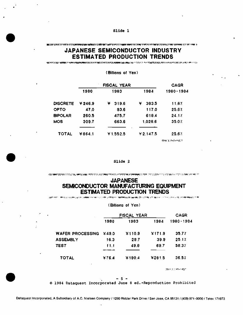
S l ide 1
JAPANESE SEMICONDUCTOR INDUSTRY ESTIMATED PRODUCTION TRENDS
(Billions of Yen)
DISCRETE
OPTO
BIPOLAR
MOS
TOTAL
1980
¥246 .9
47.0
260.5
309.7
¥864.1
FISCAL YEAR
1983
¥ 319.6
93.6
475.7
663.6
¥1.552.5
1984
¥ 383.5
117.0
618.4
1.028.6
¥2.147.5
CAGR
1980-1984
11.6^
25.6?,
24.1^
35.0J!
25.6?
; ™ . I F : : E PuTrf-iUE.-T
Sl ide 2
JAPANESE SEMICONDUCTOR MANUFACTURING EQUIPMENT
ESTIMATED PRODUCTION TRENDS yj^'X^y. tf(^-'.y,:_,'..^x^,^:'.^i^r^~^-:/'JOqi:!6;--'^ ^.iffifjeftaty:^^.:^^'.•^/^;fi^ ' - ^ • ' ' . • • f - ' « t V * "••At"--'^.? ••••' ^•-•-> >^;'..^ ^-';^X ^ »:<-Xi(«-IW^SJ--: "^ '
(Billions of Yen)
FISCAL YEAR
1980 1983
CAGR
1984 1980-1984
WAFER PROCESSING ¥49.0 ¥110.9 ¥171.9 35.7?
ASSEMBLY 16.3 29.7 39.9 25.12!
TEST 11.1 49.8 69.7 58.3?
TOTAL ¥76.4 ¥190.4 ¥281.5 36.52
jriijc :r : » I T M O ; I E ;
- 5 -1984 Dataquest Incorporated June 8 ed.-Reproduction Prohibited
Dataquest Incorporated, A Subsidiary of A.C. Nielsen Company /1290 Ridder Park Drive / San Jose, CA 95131 / (408) 971-9000 / Telex 171973

Sl ide 3
MAJOR JAPANESE EQUIPMENT MANUFACTURERS PRODUCTION TRENDS
(Billions of Yen)
ANDO-ELECTRIC APPLIED MAT.--JAPAN CANON DISCO NIKON SHINKAWA TAKEDA RIKEN TOKYO ELECTRON TOKYO-OHKA ULVAC
TOTAL OF ABOVE COMPANIES
1980
¥ 7.3 3.0
10.0 6.6 3.0 7.4 9.4
19.2 5.7 8.0
V79.6
FISCAL YEAR 1983
¥ 11.5 15.0 15.0 11.4 18.4 14.0 23.0 38.0 11.5 13.0
¥170.8
1984
¥ 16.2 24.0 21.0 15.4 30.0 20.2 32.4 53.0 15.6 18.0
Y245.8
CAGF 1980-1S
2 2 . n 68 .2/ 20.47 23.6 2: 77.8/ 28 .5/ 36 .3/ 28 .9/ 28 .6/ 22 .5/ 32 .6/
OURuE r«-^0'.c;-T
S l ide 4
NEW PLAYERS IN JAPAN
SEMICONOUCTOR EQUIPMENT AND MATERIALS
MINEBEA MINIATURE BALL BEARING MANUFACTURER--TESTING EQUIPMENT
KOKUSAI SPUTTERS AND CVD EQUIPMENT--MOVING INTO ION BEAM EQUIPMENT
KOMATSU TOP CONSTRUCTION MACHWERY MANUFACTURER--EPrrAXIAL GROWING
NPPON MINING CRUDE OIL Ah© COPPER REFINING-ELECTRONIC MATERIALS
KOBE STEEL CO. STEEL COMPANY--SEMICONDUCTOR PLATING--THROUGH JOINT VENTURE WITH KITAMURA MEKKI (50 - 50 / J
- 6 -1984 Dataquest Incorporated June 8 ed.-Reproduction Prohibited
Dataquest Incorporated, A Subsidiary of A.C. Nielsen Company /1290 Ridder Park Drive / San Jose, CA 95131 / (408) 971-9000 / Telex 171973

Slide 5
NEW PLAYERS IN JAPAN (Continued)
SEMICONDUCTOR EQUIPMENT AND MATERIALS
YOKOGA W A - HOKLSHIN
SHOWA OIL CO.
SUMISHO ELECTRIC SYSTEMS
TOYO SODA
KISHIMOTO SANGYO
M A J O R IhOUSTRlAL MEASURING EC3UIPMENT MANUFACTURER--ENTERED LINEAR IC TEST EQUIPMENT MARKET
OIL RERNING COMPANY--SILICON SINGLE-CRYSTAL SOLAR CELLS AND S O L A R BATTERIES
TRADING COMPANY--MANUFACTURES DRY ETCHING MACHINES DEVELOPED BY GCA USA
CHEMICALS--PHOTO MASK MAKING
TRADING COMPANY--MAMJFACTURES WAFER TRANSPORT SYSTEMS
• y-i 'yw;- <Aw-i"j:<^-:
r.,rv^«^.*;Vj<^;.:^^;-^_j-^jyyvr;^..^( ?
S l ide 6
PLANT SITING IN THE U.S.
JAPANESE COMPANIES
INTERNATIONAL LEADFRAME (MITSUI) KOHSAKUSHO- -LEADFRAMES KYOCERA--PACKAGES OSAKA TITANIUM--SILICON WAFERS SHINETSU HANDOTAI--SILICON WAFERS SHINKO ELECTRIC--LEADFRAMES
- 7 -O 1984 Dataquest Incor]?orated June 8 ed.-Reproduction Prohibi ted
Dataquest Incorporated, A Subsidiary of A.C. Nielsen Company / 1290 RIdder Park Drive / San Jose, CA 95131 / (408) 971-9000 / Telex 171973

Slide 7
PLANT SITING IN JAPAN
U.S. AND EUROPEAN COMPANIES
FAIRCHILD TEST HOECHST (HAS R&D LAB)--NEW FACTORY. 1985 LTX--NEW FACTORY. 1985 MATERIALS RESEARCH CORP. (MRC) MONSANTO--NEW FACTORY, 1985 SHPLEY (PHOTO RESIST)--UNDER CONSTRUCTION TELEDYNE
S l ide 8
JOINT VENTURE TRENDS r ; i , r^ ( , 'V , 'A: ? uys^fft^K^v - ^ ' ^ - U ^ * ? ' - - ' ' \ ' ^ ^ ^ -^Wf^ ' l i f 'V^ .-, -».•. ^i.-; - •;„i,|j^i^.Tx'l.--•!->.x "> ^i^.-^, , - ; v v • , ' i - . v - - 'V -^ •'WVy'W'•^•'-VV< '*rf\-•'- ' ; " " *** US?"^ •
1984
U.S. COMPANY
GENUS U.S.A.
INTEGRATED AUTOMATION
MENTOR GRAPHICS
VEECO
GEN RAD
HEWLETT-PACKARD
JAPANESE COMPANY
C. ITOH
KISH»^OTO
MARUBENI HYTEC CO.
KOKUSAI
TOKYO ELECTRON
YOKOGAMA - HOKUSHIN
PRODUCT
CVD
CVD
GRAPHICS
ION BEAM ETCHING EQUIPMENT
TESTING EQUIPMEN'
LINEAR IC TEST EQUIPMENT
- 8 -© 1984 Dataquest Incorporated June 8 ed.-Reproduction Prohibited
Dataquest Incorporated, A Subsidiary of A.C. Nielsen Company /1290 Bidder Park Drive / San Jose, CA 95131 / (408) 971-9000 / Telex 171973

Slide 9
'5^JriJ!!^W^:!*iJili;''i:!*?'^v''^<:v?f*!W^ ;l i;::i:"' !i':* !ri!i ; 'V^
JOINT VENTURE TRENDS (Continued)
1984
U.S. COMPANY
DOW CORNING (HEMLOCK S/C)
ANICON
ULVAC
KAYEX USA (SUBSDIARY OF
GENERAL ELECTRIC)
JAPANESE COMPANY PRODUCT
SHINETSU HANDOTAI MATERIALS
suMrroMo ELECTRONIC CVD EQUIPMENT SYSTEMS
L'AIR LIQUDE
KOYO LINDBERG
PLASMA ETCHING TECHNOLOGY
CRYSTAL GROWING. SUCING. AND POLISHING EQUPMENT
S l ide 10
REST OF WORLD SEMICONDUCTOR INDUSTRY
TOTAL
(Millions of Dollars)
DISCRETE
OPTO
BIPOLAR
MOS
1980
S416
120
307
143
FISCAL YEAR
1983
$ 455
150
464
450
1984
$ 531
175
610
721
CAGR
1980-1984
6.3%
10.0 J!
18.7?
50.0^
$986 S 1.5 19 S2.037 20.0?
^v'JtCt W
- 9 -© 1934 Dataquest Incorporated June 8 ed.-Reproduction Prohibited
Dataquest Incorporated, A Subsidiary of A.C. Nielsen Company /1290 Ridder Park Drive / San Jose, CA 95131 / (408) 971-9000 / Telex 171973

Slide 11
•f!t-j«i':« •:^;^^^3f5*-'r's^^^i;^*.^??;^''^5J''r^'^?^?''^ii<'i^
KOREAN SEMICONDUCTOR SALES AND INVESTMENTS
(Millions of Dollars)
KOREAN ELECTRIC COMPANY
SAMSUNG SEMICONDUCTOR
GOLD STAR SEMICONDUCTOR
KOREAN INSTITUTE OF ELECTRONIC TECHNOLOGY (KIET)
HYUNDAI ELECTRONICS
DAEWOO ELECTRONICS
TOTAL
SALES 1983 1984
$30
25
5
1
0
1
$62
£
Jl
45
45
15
2
1
2
110
INVESTMENTS 1983 1984
$15
20
15
6
25
10
$91
$ 25
60
45
6
45
20
S201 'IW'r i-Tr-.y]^--
Slide 12
SUMMARY
• 1984 JAPANESE SEMICONDUCTOR GROWTH 38.3 PERCENT IN YEN AND 44 PERCENT IN U.S. DOLLARS
• 1984 JAPANESE SEMICONDUCTOR EQUIPMENT GROWTH 48 PERCENT IN YEN AND 55 PERCENT IN U.S. DOLLARS
• TEN JOINT VENTURES BETWEEN JAPAN AND THE WEST AS OF APRIL 1984
• TEN MAJOR NEW PLAYERS IN THIS EXPLOSIVE INDUSTRY
• 1984 ROW SEMICONDUCTOR GROWTH 34 PERCENT
• 1984 KOREAN SEMICONDUCTOR CAPITAL INVESTMENTS TWO TIMES SALES REVENUES
- 10 -1984 Dataquest Incorporated June fi ed.-Reproduction Prohibited
Dataquest Incorporated, A Subsidiary of A.C. Nielsen Company / 1290 Ridder Park Drive / San Jose, CA 95131 / (408) 971-9000 / Telex 171973

EIEJ Code: Newsletters
A SECOND NTT TAKES SHAPE
Five Japanese companies are making a bold move into the telecommunications business in anticipation of the divestiture of Nippon Telegraph and Telephone (NTT) next year. Kyocera, Sony, Ushio Electric, Secom, and Mitsubishi Corporation have announced that they will establish the "Second NTT Planning Company" on May 31. Headed by Shingo Moriyama, Vice President of Kyocera, the new company will be capitalized at ¥1.6 billion ($7.0 million) and will also involve twenty other companies, including telecommunication manufacturers, banks, securities companies, and trading houses. The five founding companies will hold 50 percent ownership; stock participation outside the initial 25 companies will be available in mid-July. As shown in Table 1, the five companies are well-positioned technically and financially.
The Second NTT Planning Company plans to build a $130 million fiber-optic link along expressways between Tokyo and Osaka, to be operational in 1988. This system will offer phone and data services, and parlay the technical expertise of the five founding companies in large-scale construction projects and home electronics. It will compete directly with NTT's Information Network System (INS) which is scheduled for nationwide operation by 1987 (see our discussion of NTT's INS development plans in the DATAQUEST JSIA notebook. Section 1.2-23). However, Kyocera believes that the new service will be immediately profitable since its rates will be based on the initial link in the heavily used Tokyo-Nagoya-Osaka corridor, not on a nationwide network as with NTT's INS program. An independent survey estimates that fees for the second NTT service would be only 20 percent of NTT's current rates.
Although Yoshinori lida, an executive with NTT's New York office, said NTT welcomes the competition because it would justify the deregulation process, DATAQUEST believes that approval of the second NTT system by the Ministry of Posts and Telecommunications (MPT) will not be easy. Traditionally, MPT has been very protective of NTT, as shown in the recent value-added network (VAN) controversy with the United States. The construction of a second NTT network would cause substantial losses in revenue to NTT's $120 billion INS System—something that MPT or NTT is unlikely to welcome. Moreover, approval of the new system is likely to
© 1984 Dataquest Incorporated May 30 ed.-Reproduction Prohibited
1 no i f j l r*nT iTiT f *n» rfltiL>I [ f * t i t* l * f l r i qirf !lM *TP'I?1*1 • i l l *^J in*'V»'M •)! I'I I Lirrn i i niHi j thtir i i i i , diUiiUD'O ULL fhe 4jut)i iQ Lfi rTriojhfli] tl* i H IDUHi ttilUfl ih((<VKm*l3 In Iftf lLi|H*T';t i4xn(Ui'i»a Ui,: i 11( ^ y i j i l ' * ' i I Urtd « n n * n j iaz >. o'c mnui il>P"n.i ii Cli)** hot COniAl^.m«llfrdm
pnrnTtl*^leufeHi{^ri i j l i lrErbt ii^*fJnirAU ii^^UUil'MccipLj'uct r#|iQ<L^LI O'l and iinjiyfJHJ b> CiATAtHlfST rnitt tai c ' l t ^ * d 4 tputVMCTK^^ UJni t InJIt.A'OLlEST • i ir* i f :H ihiu in'oHrn«irf]r.ri <HI i|fiHiiaha(tiii ^^ i in^ lKm 4 i i r i4Ui iq 1^ i F'D' tctttfii u:[;u' im« p ' In Cb"n«c tK^
.fHmitMU>'^i:||Jllldr> fri andltp* 14 hir^ >d ',iHiji ^a TFi'hl Nfmnni] HaDAlPrrl anflicr \tM\' a\'tLE'i I'ilrfNh||L^BIi Hr i»'^JfiD#l« : i* iHIitii Iri'iiI'MIIT mi(p ttt\wK 1iiri|i ri> EhFiH *\n»li It ||)iIt]i>r ihH^i ^nVIATH •'^ l^-il VlK\t*iMr,t -.\r^•^l\itllT'i '^m /r\At ^^" O' Dl/V lUEti lltguiilmq
Dalaquest Incorporated, A Subsidiary of A.C. NiBisen Company 11290 RIdder park Drive/ San Jose, CA 95131 I (JOB) 971-9000 / Telex 171973

be fiercely contested by the major Japanese telecommunications companies who would Oppose the second NTT's effort to take the "cream" of the lucrative Tokyo-Nagoya-Osaka market. They would be effectively locked out of the second NTT since the five founding companies hold majority ownership. Added to this is the fierce competition posed by the entry of the Japan National Railways, Japan Highway Corporation, AT&T, IBM, ITT, Corning Glass Works, and other foreign companies into the Japanese fiber-optics market.
Thus, we believe that the second NTT is not yet an established fact but just the beginning of a long-running controversy, as Japan attempts to deregulate its telecommunications industry. However, NTT divestiture and the formation of a second NTT will create many marketing opportunities for foreign semiconductor companies selling optoelectronic ICs, optocouplers, semiconductor lasers, and other optoelectronic devices.
Sheridan Tatsuno
Table 1
FODtNDZNG C(»1PANIES OF THE SECOND NTT
Company
Kyocera
Major Products
Ceramic IC packaging (70% of world market), OA equipment
FV1983 Revenues ($ Millions)
$ 723.4
Mitsubishi Corporation
Largest trading company in Japan; strong in heavy electrical power equipment
$31,489.4
Secom (Nihon Keibi Hosho)
Electronic security systems (60% of Japanese market
$ 127.7
Sony Consumer electronics, semiconductors, floppy disks, word processors
$ 3,277.0
Ushio Electric Halogen and xenon lamps for semiconductors, OA equipment, automobiles, and Optical equipment
S 33.6
Source: DATAQUEST
- 2 -

EIEJ Code: Newsletters
TRADITION BREAK FOR TEXAS INSTRUMENTS
INTRODtJCTION
In a sharp break with the past, Texas Instruments announced that it will join the World Trade Statistics Program, originally sponsored by the Semiconductor Industry Association. TI has also decided to participate in the Semiconductor Research Cooperative, which was founded to conduct basic research through a pooling of resources.
DATAQUEST believes that TI's willingness to provide confidential sales figures to Price Waterhouse for incorporation with statistics of other O.S, European, and, recently, Japanese manufacturers is part of a strategy to move aggressively in this currently supply-limited market. We see the Dallas-based manufacturer aggressively expanding its gate array, standard cell, and CMOS business in order to keep pace with both the Japanese and with the current U.S. market leaders. Motorola and National. It is our opinion that the CMOS semiconductor market has the highest growth potential of the industry's emerging new product opportunities.
AN AGGRESSIVE NEW STRATEGY
As shown in Table 1, TI is pursuing an aggressive strategy to capture share of the microcontroller and rapidly growing application-specific IC (ASIC) markets. In 1983, TI signed second-sourcing agreements with Seeq and General Instrument for its successful TMS7000 8-bit MCU. In the gate array field, TI has joined with Fujitsu, Japan's strongest semicustom maker, to second-source Fujitsu's bipolar and CMOS arrays. Harris will second-source TI's CMOS gate arrays, which are being designed according to military specifications under the VHSIC program.
© 1984 Dataquest Incorporated May 30 ed.-Reproduction Prohibited
Tne conleni o( ihis repori represenis our interpretation and analysis ot intormai ion generally available lo ihe public or released by 'e&ponsible individuals in the subpecl companies but is not guaranteed as to accuracy or completeness II does not contain material
provided to us m confidence by our clients Individual companies reported on and analyzed by DATAQUEST may be cl ients of ihis andior oiner DATAQUEST services This information is noi (urnished in connection with a sale or offer to sell securi i ies or in connect ion
with the sol ici tat ion o( an olfer to buy securit ies This (irm and its parent and/or i he i ' of l icers s iockholdefs or members o( their (amihes may from time to time have a long or short posit ion In the securItIes menl Ioned and may sell or buy such secIjrItIes
Dataquest Incorporated, A Subsidiary of A.C. Nielsen Company /1290 Ridder Park Drive / San Jose, CA 95131 / (408) 971-9000 / Telex 171973

Although TI's sales of CMOS devices have grown at a compound annual growth rate (CAGR) of 35.7 percent since 1980, TI has lost revenues to companies offering CMOS gate arrays, such as LSI Logic. To strengthen its position in the semicustom market, TI has moved aggressively in several directions:
• Developing a 2.0-2.5 urn CMOS process in Houston
• Merging its gate array product center and design automation into the Custom Components Division in Dallas and introducing a line of CMOS standard cell logic for integrating 54/74 logic functions
• Adapting its in-house Transportable Integrated Design Automation Language (TIDAL) to run on Apollo 32-bit type workstations
• Licensing its CAD system in exchange for second-sourcing Fujitsu's bipolar and CMOS gate arrays
• Adding 4 design centers in Europe (Bedford, England; Paris, France; Frankfurt, Germany; and Milan, Italy) to its 12 centers in the United States
• Offering two levels of design for its standard cell customers
CONCLUSION
We believe that TI's move to join the World Trade Statistics Program and form partnerships in new technologies to fill voids in its product line will prove helpful in TI's quest to regain its leadership position.
Sheridan Tatsuno Gene Norrett
- 2 -

Table 1
TI'S RECENT LICENSING AGREEMENTS AND JOINT VENTURES
Date
Feb. 83
Feb. 83
March 83
Partner
Seeq
Harris
General Instrument
Agreement
Application of Seeq's EEPROM technology to TI's TMS7000 8-bit MCU
Harris to second-source TI's 1000-and 2000-gate mil-spec CMOS gate arrays (VHSIC program)
GI to second-source • 437000 MCU
TI's 8-bit
July 83 VLSI Technology, Inc. (VTI)
VTI to second-source TI's TMS4500A 64K DRAM controller and develop new CMOS circuit for TI's 256K DRAM
July 83
Nov. 83
Jan. 84
May 84
Western Digital
General Instrument
Fujitsu
National
Mutual second-sourcing of Western Digital's communications controllers and TI's universal uP peripherals
GI to second-source TI's TMS320, an NMOS digital signal processor, and develop a CMOS version
TI to provide its CAD design for Fujitsu's bipolar and CMOS gate arrays
Second-source 32-bit MPU
Source; DATAQUEST
- 3 -

EIEJ Code: Newsletters
CAN MCC CATCH UP WITH JAPAN?
Microelectronics and Computer Technology Corporation (MCC), a consortium of 15 major American electronics companies established in 1982 to beat Japan in creating a fifth-generation computer, announced six research directors on April 10, 1984. A research director for the Software Development Program will be announced in mid-May. As shown in Table 1, MCC has selected a team of highly qualified individuals to run its research programs that are formally under way. MCC currently has 110 employees working at its temporary facility, with plans to have the participating companies lend 140 more researchers by 1985. A permanent facility will be built at the University of Texas beginning this year and is scheduled to open in the fall of 1985.
MCC was formed in 1982 by 10 American microelectronics and computer companies. Since then, 5 additional companies have become full participants or shareholders, bringing the total to 15, as shown in Table 2. Each shareholder company must commit funds and staff 'to support MCC's research program for at least three years. The entry fee is $200,000. Shareholder companies will have exclusive access to research findings for three years after the completion of the project. The research or patents may be licensed and revenues then become the property of MCC. MCC has a funding goal of $324 million, of which $30 million was committed by the founding 10 companies in 1983. In addition, the University of Texas announced on April 10 a $32 million funding package for computer science programs, consisting of $8 million from a private donor. University of Texas oil lands revenues, and private matching funds from 5 Texas foundations. Although not directly benefitting MCC, this funding will provide a local source of trained researchers in the future.
MCC has scheduled four long-range advanced technology programs, as shown in Table 3.
DATAQUEST believes MCC has the potential to achieve major breakthroughs in semiconductor and computer technology. However, the project is several years behind Japan's Fifth Generation Computer Project (1979-1991) and four years behind its Supercomputer (1981-1989) and New Semiconductor Functions Project (1981-1990). We have already observed the beginning of a "patent deluge" from these projects. The New Functions
S 1984 Dataquest Incorporated April 30 ed.-Reproduction Prohibited
Tne conieni o( this report represents our inierpretal Ion and analysis ol mlormat ion generally avai lat le lo ifie public or releasea by 'esponsible individuals in the subjecl companies bul is noi guaranteed as lo accuracy or compleleness li does not coniain maienal
provided lo us in confidence by our cl ients Individual companies reported on and analyzed by DATAQUEST may be cl ienis ol thIs a-^c or oiher DATAQUEST services This informal ion is not furnished in connection wifh a sale or of ler lo sell securmes or in connection
w i lh the sol ici fat ion of an oMer lo buy securit ies This (irm and its parent and/or ihetr off icers stockholders or members of iheir famines may from time lo time have a long or short posit ion in the securit ies mentioned and may sell or buy such securit ies
Dataquest Incorporated, A Subsidiary of A.C. Nielsen Company /1290 Ridder Park Drive / San Jose, CA 95131 / (408) 971-9000 / Telex 171973

4 Project, for example, recently submitted 147 patent applications for 3-dimensional ICs. The real question for MCC is not whether it can produce innovative research; we believe it will. But rather, can it catch up with Japan?
For more information on MCC, contact:
Dr. William D. Stotesbery Director, Government and Public Affairs Microelectronics and Computer Technology Corporation 9430 Research Blvd. Echelon Building #1, Suite 200 Austin, Texas 78759-6509 Phone: (512) 343-0860
Sheridan Tatsuno
- 2 -

i Table 1
MCC RESEARCH DIRECTORS
Research Program
Semiconductor Pacltaging and Interconnects
Director
Dr. Barry Whalen
Software Technology
VLSI/CAD
To be announced in May
Dr. John Hanne
Advanced Computer Architecture comprises 4 projects:
• Parallel Processing
Dr. Peter C. Patton
• Data Base Architectures
Dr. Eugene Lowenthal
Previous Positions
Consultant to Semiconductor Research Corp. (SRC); Manager of Software and Data Systems Laboratory, and VHSIC Program at TRW Corp.
Osborne Computer and Texas Instruments; at TI, served as VP of Data Systems Group, Manager of DSG Advanced Technology R&D Division and Design Automation
Director of University Computer Center and Associate Professor of Graduate Faculties of Aerospace Engineering, Mechanics, and Computer Science at the University of Minnesota
Director of Strategic Planning at Intel's System Division; Chief Architect of the System 2000 at MRI Systems Corp.
(Continued)
- 3 -

4 Table 1 (Continued)
MCC RESEARCH DIRECTORS
Research Program
• Human Factors Technology
Director
Raymond Allard
Artificial Intelligence/ Knowledge-Based Systems
Dr. Woodrow Bledsoe
Previous Positions
Vice President at Control Data; oversaw development of Cyber 205; design manager of 3200 and 3300 series computer architectures
Ashbel Smith Professor of Mathematics and Computer Sciences and Chairman of the Mathematics Department at the University of Texas, Austin (on leave); now President of the American Association of AI
Source: Microelectronics and Computer Technology Corporation
- 4 -

Table 2
MCC CORPORATE OFFICERS AND BOARD OF DIRECTORS
Name
Corporate Officers
Admiral B.R. Inman Palle Smidt Dr. John Pinkston R.G. Rutishauser George D. Black
Position
President/CEO/Board Chairman Senior VP/Plans and Programs VP/Chief Scientist VP/Finance and Administration VP/Human Resources
Company
U.S. Navy* Sperry* Nat'l. Security Agency* Control Data* RCA*
MCC Shareholders and Board of Directors
Philip W. Arneson George M. Scalise Ryal R. Poppa Robert M. Price F. Grant Saviers Michael F. Maguire James J. Renier Allan M. Norton Robert E. Caldwell William G. Howard, Jr. Gregory Harrison Thomas T. Tang William C. Hittinger Robert L. Cattoi Don O. Neddenriep
*Previous employer
President Sr. VP/Chief Admin. Officer President/CEO/Chairman President/CEO VP/Storage Systems Develop. Sr. VP/Sector Executive President/Information Systems VP/Technical Operations Sr. VP/Engineering and Tech. VP/Corporate Director VP/Corporate Services VP/Research and Development Executive VP VP/Corporate Engineering Group VP Product Division
Allied Corporation AMD BMC Industries Control Data Digital Equipment Harris Honeywell Martin Marietta Mostek Motorola National Semiconductor NCR RCA Rockwell International Sperry
Source: Microelectronics and Computer Technology Corporation
- 5 -

Table 3
MCC RESEARCH PROGRAMS
Program
Alpha-Omega
CAD/CAM
Software
Chip Packaging
Length
10 Yrs.
Projected Funding
$150 M
8 Yrs.
7 Yrs.
6 Yrs.
$88 M
$56 M
$30 M
Total Project 31 Yrs. $324 M
Research Focus
Artificial intelligence Parallel processing Data base system management Voice and character recognition
VLSI design equipment
Programs for artificial intelligence and knowledge-based systems
Advanced semiconductor Packaging and interconnect technologies compatible with automatic assembly at circuit and system levels
Source: DATAQUEST
- 6 -

Dataquest RESEARCH BULLETIN
EIEJ Code: Newsletters
MITI BOWS TO U.S. DEMAND FOR SOFTWARE COPYRIGHT PROTECTION
U.S. officials were recently informed by the Ministry of International Trade and Industry (MITI) that the agency would not submit its controversial proposal for a software patent law to the Japanese Diet. This action comes after several months of vigorous protest from U.S. negotiators who argued that the MITI proposal violated the Berne Convention, an international copyright pact, and would effectively push U.S. software makers out of the Japanese market.
Interpreted as a victory by U.S. negotiators, this decision is also noteworthy because it reflects the strong dissension among the Japanese ministries over important high-technology issues. As shown in Table 1, Japanese officials are divided into two camps: those supporting MITI's proposal for a 15-year protection and mandatory licensing law, and those supporting the Ministry of Education's Cultural Agency proposal for a 50-year software copyright law. The major point of contention is over definitions.
MITI, a strong proponent of the computer industry, defines software as an industrial product requiring patent protection, while the Cultural Agency defines it as intellectual property that should be accorded the same copyright protection as books and movies. MITI believes that mandatory disclosure and licensing would enable Japanese industry to develop software more rapidly and would make available to the public vital software in such areas as medical treatment. A 15-year protection period would help Japan, a major software importer, to promote software development, distribution, and use. The Cultural Agency disagrees, arguing that mandatory disclosure and shortening the protection from 50 to 15 years would discourage software development. Table 2 summarizes the major differences between the two ministries.
MITI's decision is clearly an effort to avoid worsening trade friction with the West at a time when sensitive issues such as value-added networks (VAN), satellites, the U.S. unitary tax, and domestic content laws are being discussed in both capitals. Nevertheless, DATAQUEST believes that a compromise version of MITI's proposal will be introduced to the Diet in the near future.
Sheridan M. Tatsuno
© 1984 Dataquest Incorporated April 12 ed.-Reproduction Prohibited
The conieni ot this report represenis our inierpretaiion and analysis ot information generally available to Ihe public or released by responsib le individuals tn the sudiecf companies bul is nol guaranteed as to accuracy or completeness It does not contain material
provided io us in contidence by our cltenis Individual companies reported on and analyzed by DATAQUEST may be cl ients ot this and/or other DATAQUEST services This information is not (urmshed In conf iecl ion with a sale or oftef to sell securit ies or m connection
wIth the sol ic I tai ion of an offer to buy securIties This fIrm and its parent and'or their otdcers stockholders or members o ' iheIr families may from time to ti i j ie have a long or short posit ion in ifie securit ies mentioned and may sell or buy such securit ies
Dataquest Incorporated, A Subsidiary of A.C. Nielsen Company /1290 Ridder Park Drive / San Jose, CA 95131 / (408) 971-9000 / Telex 171973

Table 1
JAPANESE LINE-UP IN SOFTWARE CONTROVERSY
15-Year Patent Law
MITI
Japan Electronic Industry Development Association (JEIDA)
Japan Business Machine Makers Association
Japan Communication Industries Association
50-Year Copyright Law
Cultural Agency (Ministry of Education)
Ministry of Posts & Telecommunications
Table 2
MINISTRY POSITIONS ON SOFTWARE PROTECTION
Objective
Right of Use
Developer's Personal Rights
MITI
Program protection and licensing; development of national economy
Control use of illegal software programs
Important not to Impede software development and diffusion
Cultural Agency
Copyright protection and promotion of cultural development
Not regulated
Protection of developer's copyright
User Protection
Registration System
Mandatory release of programs vital to public welfare
Release and promotion of software programs; price stabilization
Not regulated
Record of third-party transactions
Source: DATAQUEST
- 2 -

Dataquest RESEARCH BULLETIN
EIEJ Code: Newsletters
JAPANESE NONTARIFF BARRIERS—AN UPDATE
SUMMARY
Nontariff barriers are implicit or explicit policies that prevent one or more foreign countries from competing in a particular marketplace. The Japanese marketplace has become a difficult one for foreign competitors to penetrate. This research bulletin addresses the following three currently disputed Japanese nontariff barriers: value-added networks (VANs), software, and satellites.
Value-Added Networks
VANs—value-added networks—are the subject of one trade dispute between the United States and Japan. VANs are data transmission services that allow dissimilar computers to communicate with each other. Services such as electronic mail, credit card checks, airline reservations, and hotel reservations are handled through VANs. In all of these areas, the United States is technically far ahead of any other country, including Japan.
VANs are one of the first in a series of Japanese government-driven programs designed to expand data communications in Japem. Such semiconductors as data conversion circuits, codecs, filters, and other telecommunications chips can expect to see an expanding market due to this push.
On January 31, 1984, the Japanese Ministry of Posts and Telecommunications—which regulates the country's telephone monopolies, Nippon Telegraph and Telephone (NTT) and Kokusai Denshin Denwa (KDD)—decided to allow U.S. companies to compete in the large-scale VAN marketplace in Japan. However, on February 9, a government advisory panel urged the exclusion of all companies with more than 20 percent foreign ownership from Japan's VAN market as a protective measure for Japan.
The dispute is currently still raging, with senior Japanese officials stating that the 20 percent proposal is not a final one. If it were to stand, it would eliminate such U.S. giants in the field as IBM and AT&T.
© 1984 Dataquest Incorporated Feb. 27 ed.-Reproduction Prohibited
Tne conlen
proviOed to
with the sol
ot ihis report represents our inierpretation and analysis ol mformal ion generally available to Ihe public or released by responsible mdivIduais m tfie subject companies but is not guaranteed as to accuracy orcornpleten
s m conl idence by our cl ienis Individual companies reported on and analyzed by DATAQUEST may be cl ients o l this and/or other DATAQUEST services This mlormat ion is not furnished in connect ion wi ih a sale or offer
citation o( an olfer to buy securi l ies TIMS firm and iis parent and/or their oHicers stockholders or members ol their (amilies may from i ime to time have a long or short posit ion m the securit ies mentioned and may sell c
o s e
r bu
It does not contain material
1 securit ies or m connect ion
y such securities
Dataquest Incorporated, A Subsidiary of A.C. Nielsen Company / 1290 Ridder Park Drive / San Jose, CA 95131 / (408) 971-9000 / Telex 171973

Software
Another dispute involves software copywriting. MITI-backed legislation would replace current international copyright protection (which lasts until 50 years after the author's death) with a limited 15-year protection for software. Most damaging to foreign firms, however, is the proviso that would require software suppliers to license their software to Japanese firms, allowing the Japanese companies to sell the software without paying royalty fees. This would essentially bar aU U.S. and other foreign firms from the large Japanese software market.
Satellites
Another area in which the U.S. has a strong technological edge is satellites. Japan presently does not produce satellites; yet, under Japginese law, Japanese firms must be the prime contractors for satellite development. While on the face of it this requirement should completely eliminate the United States 6is a supplier of satellites to Japan, Ford and Hughes have both in fact received contracts from major Japanese firms to develop satellites.
Japanese firms are apparently unhappy with current Japanese government policy regarding satellite procurement; therefore, this may prove to be the easiest nontariff barrier to break down.
Patricia S. Cox;
- 2 -

EIEJ Code: Newsletters
THE JAPANESE CHALLENGE-ONE MAN'S OPINION
SUMMARY
Dr. Ezra Vogel, Director of the Program on U.S.-Japan Relations and Professor of Sociology at Harvard University, recently spoke to the Japan Society of Northern Ceilifornia on Japan's continuing challenge to the United States. Dr. Vogel, who recently returned from a year-long sabbatical in Japan, believes that Japan wiU continue to gain strength as an international economic power for the following three reasons:
• Japan is far ahead of any western nation in the "new industrial revolution" of flexible manufacturing systems and robotics.
As a result of increased office automation, Japan's service sector will become a much greater part of its economy, and wiU present the major challenge to the western world.
Japan as a nation demonstrates a real concern for its society as major industrial changes occur.
JAPANESE MANUFACTURING
The Japanese have long been acknowledged as experts and leaders in manufacturing techniques. In addition to the widely publicized use of robotics in factory automation, a new technique, the flexible manufacturing system (FMS), is profoundly affecting today's Japanese manufacturing.
FMS utilizes computerized, numerical control of tooling devices in machining centers. It allows tools to be changed automatically, it links different machines together, and it sets the stage for completely automated assembly lines that require only one operator to monitor the entire operation via a video screen.
Dr. Vogel believes that Japan's software experts have been concentrating their work in the assembly/production field rather than in the packaged software field. Thus the West's perception that the Japginese are not knowledgeable about software or lack the ability to produce it is fallacious.
© 1984 Dataquest Incorporated Feb. 9 ed.-Reproduction Prohibited
completers Tfie conieni of this report reoresents our Inierpretalion anid analysis o( information generally available to ihe pulDhc or released by responsible individuals in ihe subject companies but is not guaranteed as lo accut
provided to us m conl idence by our cl ienis Individual companies reported on and analyzed by DATAQUEST may be clients of this and/or other DATAQUEST services This mlormal ion is not furnished m connection wi ih a sale or offer
with the sol ici tat ion of an offer to buy securit ies This firm and its parent and'or their off icers sfocdholdeis or members of their families may from i ime to time nave a long or shofl posit ion m the securit ies mentioned and may sell
li does not contain material
securit ies or m connect ion
such securit ies
Dataquest Incorporated, A Subsidiary of A.C. Nielsen Company /1290 Ridder Park Drive / San Jose, CA 95131 / (408) 971-9000 / Telex 171973

It is interesting to note that there are approximately three times as many electrical engineers per capita in Japan as there are in the United States. (Another interesting fact is that while Japan has 12,000 practicing attorneys, compared to 600,000 in the United States, Japan's population is only about half that of the United States.) The engineers who work on research and development of a product are the same ones who are involved in production line work on the product, thereby ensuring a very close connection between R&D and actual manufacturing.
SERVICE SECTOR
Office automation activity has increased tremendously in Japan over the last several years. The use of personal computers and other office automation equipment in Japan is a dramatic change because Japanese offices, in contrast to Japanese factories, traditionally have been very inefficient. Until recently no easy-to-use Japanese typewriter existed. With over 2,000 kanji characters, the process of typing in Japanese was very laborious, and in fact, secretaries were often chosen for their legible handwriting.
This situation has changed with advances in microprocessors and large (1Mb) ROMs, which now allow word processors, using a katakana—phonetic—keyboard, to produce kanji characters. (For an explanation of the Japanese language and alphabet, please refer to EIEJ Section 3.6, Japanese Language.) The previous lack of a viable typewriter is the primary reason for the current proliferation of copying machines and facsimile machines in Japan.
AS a result of these changes, Japanese office productivity should experience great improvement. MITI now views the service sector as-a high growth area, and will begin to target this area for expansion. There will be an increased emphasis on software for personal computers and minicomputers.
The promotion of service industries abroad will eliminate the foreign trade barriers present on commodities such as semiconductors and other equipment. As an example, Japanese banks finance Japanese factories built in the United States; they also have bought out some U.S. banks, especially in California. The same sort of thing can happen in other service areas, such as insurance, real estate, and financial services. This represents a definite penetration of the U.S. economy, but not one that is as easily quantifiable as manufactured goods.
CONCERN FOR SOCIETY
Japanese companies are known for loyalty to their employees. This extends beyond lifetime employment to the areas of continuing education and retraining of personnel, concepts that are foreign to most western companies. Large Japanese companies such as NEC maintain complete educational programs for their employees, so that engineers, for example, wiU be kept up-to-date on the latest technologies and information, and their skills wiU not become obsolete. Many companies retrain personnel who are in ot)solete jots, so that they can remain with the company in another position. To the best of our knowledge, Japanese companies' educational and training programs are more comprehensive gind receive greater emphasis than any similar U.S. programs. Overall, Japanese compsinies have a great sense of responsibility toward their employees.
- 2 -

Because of continuing education and retraining, Japanese employees wiU probably not face the problems faced by many U.S. employees who are losing jobs in declining industries such as steel, and find themselves unprepared for any other kind of work.
CONCLUSIONS
Dr. Vogel concluded his remarks by presenting his ideas about what the United States can do to respond to the Japanese challenge:
• Think about competitive problems by developing nongovernmental analytical groups in Washington that would provide Congress with analyses on which to base legislation.
• Train more people in Japanese language, history, and culture, and put their skills to use in business. In this marmer, American business will have employees versed in Japanese language and culture, the only attributes that really allow American businesses to successfully penetrate the Japanese market. There are great forces of conservatism in place in Japan, and the only way to break through these is through true knowledge of Japan and the Japanese.
• Get the American point of view into the Japanese press. As an example of the need to represent the American view, Dr. Vogel reported that, regarding the IBM-Hitachi case, IBM was presented in the Japanese press as a "bad buy" who tricked Hitachi.
• Form more cross-culture organizations, such as joint ventures, especially in scientific and technical areas.
Patricia S. Cox
3 -

EIEJ Code: Newsletters
JAPAN DEVELOPMENT BANK LOANS AVAILABLE TO FOREIGN COMPANIES
SUMMARY
For foreign companies interested in exporting high-technology equipment to Japan or opening research centers and plants there, the Japan Development Bank (JDB) is a potential source of low-cost funds. Since 1968, JDB has issued ¥117 billion in loans to foreign capital-affiliated enterprises (those whose foreign capitalization is 50 percent or more). In fiscal 1983 (April to March 31), 13 companies received a total of ¥17 billion, or about ¥1.3 biUion ($5.4 million) each, as shown in Table 1.
Table 1
JAPAN DEVELOPMENT BANK LOANS TO FOREIGN COMPANIES
Fisca l Year
1979
1980
1981
1982
1983
(¥
Total Funds B i l l i on )
4 . 9
10.4
12.8
11.0
17.0
Exchange Rate
(Yen/$)
220
225
220
250
240
Dollar Value
(^Million)
22.3
46.2
58.2
44.0
70.8
Number of
Companies
9
6
8
5
13
Per Company
(^Mill ion)
2 . 5
7 .7
7 .3
8 .8
5 .4
Source: Japan Development Bank
© 1984 Dataquest Incorporated Feb. 1 ed.-Reproduction Prohibited
Tne content of this report repfesents our mterpretai
provided to us ir> confidence by our clients Individual
w im the solicitat ion of an o l le f lo buy securit ies Thi
on and analysis ol in lormal ion generally available \o
companies reported on and analyzed by DATAQUEST
(irm and ils parent and/or their ot i icers slocKholder
he pub l ic or released by responsible individuals m the subiec
may oe cl ients ot this and/or oiher DATAQUEST services This
s or membefs of iheif families may from time to time have a I
companies, but is not guaranteed as to accuracy or completeness II does not contai
information is not furnished in connection with a sale or offer to sell secuniies or in c
ang or short posit ion in the securities mentioned and may sell or buy such securit ies
n material
• nnection
Dataquest Incorporated, A Subsidiary of A.C. Nielsen Company /1290 Ridder Park Drive / San Jose, CA 95131 / (408) 971-9000 / Telex 171973

NEW LOW-INTEREST LOAN PROGRAM FOR MANUFACTURING PLANTS
In order to lessen trade friction with other countries, JOB has expanded its loan program to promote foreign imports and investments in Japan. Beginning in fiscal 1984, about ¥13 billion ($55 million) in special loans with a 7.8 percent interest rate win be issued to foreign companies for up to 40 percent of their investments under the "International Cooperation Loan System." This compares with the 8.4 percent loans under the existing JDB program. As of October 1983, 20 companies had applied for these low-interest loans, of which 12 projects have been selected to be financed in fiscal 1984. The four IC-related projects selected are shown in Table 2.
Table 2
FOREIGN IC PLANTS TO BE FINANCED IN FISCAL 1984
Foreign Company
Japan Burr Brown
Nippon Motorola .
Intel
Fairchild
Cost ( B)
1.0
2.0
40.0
6.5
Loan (¥B)
0.4
0.8
16.0
2.6
Amoun t* ($M)
1.7
3.4
68.1
11.1
Construction Period
Jan.-Aug. 1984
Dec. 1983-Sept. 1984
Fiscal 1984
Fall 1983-Fall 1984
Project
Hybrid IC plant in Tsukuba Science City
Hybrid IC plant in Aizu Wakamatsu
IC plant
Bipolar logic plant in Isahaya industrial park, Nagasaki Prefecture
*Maximum a v a i l a b l e ; not ac tua l amount Note: I n t e r e s t r a te 7.8 percent , 40 percent r a t i o , 10 years
Source: Japan Development Bank

WHO IS ELIGIBLE
Foreign companies that invest in regional development, new technologies, pollution prevention, energy and resource projects, and urban development are eligible for funding, as shown in Table 3. The Ministry of International Trade and Industry (MITI) and the prefectures place special emphasis on new technologies, such as semiconductors, computers, biotechnology, and new materials, because of their potential for creating new jobs. In June 1983, Materials Research Corporation of New York was the first company to receive a preferential loan for ¥350 million ($1.46 million) to finance its $3.2 million sputtering machine factory in Kyushu's Oita Prefecture. The loan has an 8.4 percent interest rate for a period of 10 years. Since then, JDB has lowered the interest rate to 7.8 percent under the new International Cooperation Loan System.
Table 3
TYPES OF PROJECTS ELIGIBLE FOR JDB LOANS
Loan Area Types of Projects
Regional Development
Plant construction in less-developed regions; warehouses, distribution centers, and hotels in local cities
Technology Development
New technologies such as semiconductors, biotechnology, new materials, and computers
Pollution Prevention and Safety
Antipollution facilities, safety testing labs for pharmaceuticals, agrochemicals, and building construction
Resource and Energy Projects
Facilities for resource and energy conservation, oil-to-coal switching technology, and oil and LPG Storage
Urban Development Construction of large-scale distribution centers, warehouses, and urban redevelopment
Other Ocean shipping, ocean development facilities, large hotels in urban areas
Source: Japan Development Bank

>
JDB LOAN TERMS
Under the JDB loan program, the terms of the loans vary according to the type of project proposed, as shown in Table 4. Loans to high-technology companies are covered by the Law for Temporary Measures for Special Machinery and Information Industries, which aims to raise the level of productivity and technological research throughout Japan.
Table 4
LOAN TERMS UNDER JOB'S REGULAR LOAN PROGRAM
Area
Reg iona l Development
Technology Development
P o l l u t i o n P r e v e n t i o n and Sa fe ty
Resource and Energy P r o j e c t s
Urban Development 8.4% ( s p e c i a l r a t e s 40%-50% 5 t o 15 y e a r s 7.3%-8.3%)
*7.8 percent under new International Cooperation Loan System
Source: Japan Development Bank
Interest Rate
8.4%
8.4% (special rates 7.3%-8.3%)*
7.5% 8.0%
8.4% (special rates 7.3%-8.3%)
Amount Covered
30%-
40%
50% 50%
40%-
-50%
•50%
Loan Period
7 to 10 years
5 to 10 years
First three years thereafter
3 to 15 years
-4

NATIONAL AND LOCAL TAX INCENTIVES
Foreign companies are eligible for special depreciation on production equipment under the Special Taxation Act. In addition, tax incentives under the Industrial Relocation Promotion Law for investments in undeveloped industrial areas and local tax incentives from the prefectures are available to foreign companies. For example, Kumamoto Prefecture in Kyushu (the southern island known as "Silicon Island") offers complete business tax exemptions for three years on plants over ¥15 million ($64,000) in existing industrial areas and reduced real estate taxes (by 1.26/100) for three years on plants over ¥100 million ($425,000) in new industrial areas. Currently, MITI is coordinating foreign plant siting as part of its strategy to create "technopoli," or high-tech industrial areas, throughout Japan. MITI's Industrial Location Guidance Division provides information on industrial parks and tax incentives and offers siting assistance. The prefectures compete with each other to a t t rac t foreign plants by offering a variety of incentives and services that are usually negotiable on a case-by-case basis.
NEW LOW-INTEREST LOAN PROGRAM FOR IMPORTERS
In fiscal 1984 (April 1, 1984 to March 31, 1985), JDB will also offer low-interest loans to Japanese leasing companies that import high-technology equipment from advanced industrial nations. A ¥2.0 billion ($8.5 million) fund has been established to provide 7.8 percent loans to leasing firms importing computers, peripherals, communications equipment, medical equipment, and machine tools. This program is part of MITI's import promotion policy that was recently adopted to reduce trade friction with Japan's trading partners. Although minimal in size, DATAQUEST believes these JDB loans are important because they are a signal to Japanese banks that the import activities are being promoted by MITI.
FOR MORE INFORMATION
For more information about Japan Development Bank loans, contact the following offices.
Head Office
9-1, Otemachi 1-chome Chiyoda-ku, Tokyo 100, Japan Phone: (03) 270-3211 (switchboard)
(03) 245-0439 (nonbusiness hours) Cable: DEVEBANK TOKYO Telex: J24343 DEVEBANK

. _-v
Overseas Offices
Washington, D.C. Representative Office 1019 19th Street, N.W., Suite 600 Washington, DC 20036 U.S.A. Phone: (202) 331-8696 Cable: DEVEBANK WASHINGTONDC Telex: 440084 JDBK UI
New York Representative Office 71 Broadway, Room 306 New York, NY 10006 U.S.A. Phone:(212) 269-0527 Cable: DEVBANKMIN NEW YORK Telex: 421054 KAIGIN
London Representative Office P. <5c O. Building 122-138 Leadenhall Street London EC3V 4PT, United Kingdom Phone:(01) 623-0172, 0173 Cable: JADEBANK LONDON-EC3 Telex: 888907 JDBLDN
Frankfurt Representative Office Rhein Main Center Bockenheimer Landstrasse 51-53 6000 Frankfurt am Main Federal Republic of Germany Phone: (0611) 724341, 724342 Cable: JADEBANK FRANKFURT Telex: 412946 JDBF
Sheridan M. Tatsuno
6 -


1985-1986 JSIS Newsletter Index
The 1985-1986 JSIS Newsletter Index is a quick reference guide to the EIEJ and JSIA newsletters. It is structured as follows:
• Titles are organized by both keyword and company.
Page 2 is a company list, e.g., LSI Logic.
Pages 3 to 5 are a subject list, e.g.. Economy.
• The newsletter type, month, and year follow each title listing in the Index. Refer to the EIEJ or JSIA tab, month, and year to locate a specific newsletter.
This Index will be updated quarterly.
JSIS Newsletters ©1986 Dataquest Incorporated Jan. 24

1985-1986 JSIS Newsletter Index
Compainy Newsletter Date
HEWLETT-PACKARD CO. ToshilJa Builds R&D Bridge JSIA Oct. 85
HITACHI LTD. Hitachi Unveils Plan to Ease Trade Friction JSIA July 85
LSI LOGIC CORP. Venturing into Japan: How LSI Logic Opened its Doors in Tokyo JSIA May 85
MITSUBISH ELECTRIC CORP. The New Mi t sub ish i S a i j o Factory—A Ful ly Automated F a c i l i t y JSIA Oct. 85
TOSHBA ELECTRIC CO. Toshiba Builds R&D Bridge JSIA Oct. 85
1986 Dataquest Incorporated Jan. 24 JSIS Newsletters

1985-1986 JSIS Newsletter Index
Subject Newsletter Date
ASSOCIATIONS Ninth Annual SIA Forecast Dinner: Forecasting the Recovery JSIA Sept . 85
CARTAL EXPBOITURES Japanese Market Update—Current Outlook JSIA June 85
CONFERENCES 1985 Japanese Electronics Show Worldwide Technical Meetings Dataquest's Japanese Conference Debut—Far East Industry
JSIA Dec. 85 EIEJ Sept. 85 JSIA May 85
CONSUMPTION DATA Japanese End Market Analysis Japanese Semiconductor Market Update Japanese Mcurket Update—Current Outlook Semiconductor Consumption in Japan Explodes in 1984 New Trends in Semiconductor Distribution
JSIA Oct. 85 JSIA Sept. 85 JSIA June 85 JSIA Mar. 85 JSIA Mar. 85
DISTRIBUTION New Trends in Semiconductor Distribution JSIA Mar. 85
ECONOMY The U.S. Economy: Boom or Bust? " JSIA Nov. 85 Japan Plans New Market-Opening Measures EIEJ Sept. 85 Semiconductor Gardening: Japan's Response to the Current Downturn JSIA July 85
FACIUTIES 1984 Construction Boom Creates Over-Capacity JSIA Oct. 85
GAAS Seventh Annual GaAs Symposium, November 12-14, 1985 JSIA Nov. 85
GATE ARRAYS Venturing into Japan: How LSI Logic Opened its Doors in Tokyo JSIA May 85
GOVERNBVENT Japan Plans New Market-Opening Measures EIEJ Sept. 85
JSIS Newsletters 1986 Dataquest Incorporated Jan. 24

JSIA
JSIA JSIA JSIA JSIA JSIA JSIA JSIA JSIA
Sept.
Dec. Nov. Sept. Sept. Aug. June May Jan.
85
85 85 85 85 85 85 85 85
1985-1986 JSIS Newsletter Index
Subject Newsletter Date
INDUSTRY Turning the Tide: U.S. Semiconductor Activities in Asia
I^DUSTRY TRENDS 1985 Japanese Electronics Show Japanese Semiconductor Technology Trends—Third Quarter 1985 Ninth Annual SIA Forecast Dinner: Forecasting the Recovery Japanese Semiconductor Market Update Japanese Semiconductor Technology Trends—Second Quarter Japanese Semiconductor Technology Trends First Quarter 1985 Dataquest's Japanese Conference Debut—Far East Industry Japanese Semiconductor Technology Review Fourth Quarter 1984
INFORMATION SOURCES Successful Intelligence Gathering: Dataquest's Recipe JSIA Mar. 85
ISSCC Japan Takes Center Stage at ISSCC 1985 JSIA Mar. 85
MANUFACTURING Semiconductor Mfg. Equipment: Can the U.S. Remain Competitive? EIEJ May 85
MARKET SHARE Preliminary 1985 Japanese Company Market Share Estimates JSIA Dec. 85 The Japanese Market: Sales by All Manufacturers in 1984 JSIA June 85 Japanese Market Update—Current Outlook JSIA June 85 Japanese Semiconductor Activity in the U.S.—1984 Update JSIA Feb. 85 Preliminary 1984 Market Share Estimates JSIA Jan. 85
PRODUCTION DATA Japanese Industrial Elec. Production to Reach Y11.3 T in 1989 JSIA Dec- 85 1984 Construction Boom Creates Over-Capacity JSIA Oct. 85 Japanese Electronic Equip. Production to Reach yi9 T in 1990 JSIA Oct. 85
R&D PROJECTS Japanese Semiconductor Technology Trends—Third Quarter 1985 JSIA Nov. 85 Toshiba Builds R&D Bridge JSIA Oct. 85 Japanese Semiconductor Technology Trends—Second Quarter JSIA Aug. 85
1986 Dataquest Incorporated Jan. 24 JSIS Newsletters

1985-1986 JSIS Newsletter Index
Subject Newsletter Date
R8tD PROJECTS (Contirujied) Japanese Semiconductor Technology Trends Fi rs t Quarter 1985 JSIA June 85 Japan Takes Center Stage a t ISSCC 1985 JSIA Mar. 85 Japanese Semiconductor Technology Eteview Fourth Quarter 1984 JSIA Jan. 85
ROW Dataquest's Japanese Conference Debut—Far East Industry JSIA May 85
SHIPMENT DATA Japanese Semiconductor Activity in the U.S.—1984 Update JSIA Feb. 85
START-UPS The Third Wave: The Surge in Semiconductor Start-Ups Continues JSIA Oct. 85 The Semiconductor Start-Up Boom Continues JSIA May 85
U.S7JAPAN Ninth Annual SIA Forecast Dinner: Forecasting the Recovery Turning the Tide: U.S. Semiconductor Activities in Asia U.S. euid Japanese Semiconductor Industry Interrelationships Hitachi Unveils Plan to Ease Trade Friction U.S.-Japan Semiconductor Trade Update First Quarter 1985 Venturing into Japan: How LSI Logic Opened its Doors in Tokyo U.S.-Japan Trade: East Leads West Semiconductor Consumption in Japan Explodes in 1984 Japanese Semiconductor Activity in the U.S.—1984 Update
JSIA JSIA JSIA JSIA JSIA JSIA JSIA JSIA JSIA
Sept. Sept. July July July May Apr. Mar. Feb.
85 85 85 85 85 85 85 85 85
JSIS Newsletters ©1986 Dataquest Incorporated Jan. 24

1985-1986 JSIS Newsletter Index
(Page intentionally left blank)
1986 Dataquest Incorporated Jan. 24 JSIS Newsletters

1985-1986 JSIS Newsletter Index
The 1985-1986 JSIS Newsletter Index is a quick reference guide to the EIEJ and JSIA newsletters. It is structured as follows:
• Titles are organized by both keyword and company.
Page 2 is a company list, e.g., LSI Logic.
Pages 3 and 4 are a subject list, e.g., Economy.
• The newsletter type, month, and year follow each title listing in the Index. Refer to the EIEJ or JSIA tab, month, and year to locate a specific newsletter.
This Index will be updated quarterly.
JSIS Newsletters ©1985 Dataquest incorporated Sept. 24

1985-1986 JSIS Newsletter Index
Company Newsletter Date
HITACHI LTD. Hitachi Unveils Plan to Ease Trade Friction JSIA July 85
LSI LOGO CORP. Venturing Into Japan: How LSI Logic Opened its Doors in Tokyo JSIA May 85
© 1985 Dataquest Incorporated Sept. 24 JSIS Newsletters

1985-1986 JSIS Newsletter Index
Subject Newsletter Date
CARTAL EXPENDITURES Japanese Market Update—Current Outlook JSIA June 85
CONFERENCES Worldwide Technical Meetings Dataquest's Japanese Conference Debut—Far East Industry
EIEJ Sept. 85 JSIA May 85
CONSUMPTION DATA Japanese Market Update—Current Outlook Semiconductor Consumption in Japan Explodes in 1984 New Trends in Semiconductor Distribution
JSIA June 85 JSIA Mar. 85 JSIA Mar. 85
DISTRIBUTION New Trends in Semiconductor Distribution JSIA Mar. 8E
ECONOMY
Japan Plans New Market-Opening Measures EIEJ Sept. Semiconductor Gardening: Japan's Response to tne Current Downturn JSIA July
85 85
GATE ARRAYS
Venturing Into Japan: How LSI Logic Opened its Doors in Tokyo JSIA May 85
GOVERNMENT Jajsan Plans New Market-Opening Measures EIEJ Sept . 85
INDUSTRY Turning the Tide : U.S. Semiconductor A c t i v i t i e s m Asia JSIA Sept. 85
INDUSTRY TRENDS
Japanese Semiconductor Technology Trends — Second Quarter Japanese Sem.iconductor Technology Trends First Quarter 1985 Dataquest's Japanese Conference Debut—Far East Industry Japanese Semiconductor Technology Review Fourth Quarter 1984
JSIA Aug. 85 JSIA June 85 JSIA May 85 JSIA Jan. 85
INFORMATION SOURCES Successful Intelligence Gathering: Dataquest's Recipe. JSIA Mar. 85
JSIS N e w s l e t t e r s © 1 9 8 5 D a t a q u e s t Incorporated Sept . 24

1985-1986 JSIS Newsletter Index
Subject Newsletter Date
ISSCC Japan Takes Center Stage at ISSCC 1985 JSIA Mar. 85
MANUFACTURING Semiconductor Mfg. Equipment: Can the U.S. Remain Competitive: EIEJ May 85
MARKET SHARE The Japanese Market: Sales by All Manufacturers in 1984 Japanese Market Update—Current Outlook Japanese Semiconductor Activity in the U.S.—1984 Update Preliminary 1984 Market Share Estimates
JSIA June 85 JSIA June 85 JSIA Feb. 85 JSIA Jan. 85
R&D PROJECTS Japanese Semiconductor Technology Trends—Second Quarter Japanese Semiconductor Technology Trends First Quarter 1985 Japan Takes Center Stage at ISSCC 1985 Japanese Semiconductor Technology Review Fourth Quarter 1984
JSIA Aug. 85 JSIA June 85 JSIA Mar. 85 JSIA Jan. 85
ROW Dataquest's Japanese Conference Debut—Far East Industry JSIA May 85
SHIPMENT DATA Japanese Semiconductor Activity in the U.S.—1984 Update JSIA Feb.
START-UPS The Semiconductor Start-Up Boom Continues JSIA May 85
U.S./JAP AN Turning the Tide: l.'.S. Sem.iconductor Activities in Asia U.S. and Japanese Semiconductor Industry Interrelationships Hitachi Unveils F'lar, tc Ease Trade Friction U.S.-Japan Semiconductor Trade Update First Quarter 1985 Venturing Into Japan: How LSI Logic Opened its Doors in Tokyc U.S.-Japan Trade: East Leads West Semiconductor Consumption in Japan Explodes in 1984 Japanese Semiconductor Activity in the U.S.—1984 Update
JSIA JSIA JSIA JSIA JSIA JSIA JSIA JSIA
Sept. July July July May Apr. Mar. Feb.
85 85 85 85 85 85 85 85
© 1985 Dataquest Incorporated Sept. 24 JSIS Newsletters


DataQuest 3 company of The Du 11 lScTir»d!;(rcct corporation
JAPANESE RESEARCH
NEWSLETTER
JSIS Code: Newsletters 1985-1986, JSIA 1986-31
U.S.-JAPAN SEMICONDUCTOR TRADE UPDATE: FIRST QUARTER 1986
TRADE STATISTICS
Bilateral U.S.-Japanese semiconductor trade turned up in the first quarter of 1986. This upturn followed an extremely depressed 1985, during which both sides saw sales fall dramatically.
As measured by Japan's Ministry of Finance (MOP), Japanese semiconductor exports to the United States were up 12.7 percent in dollars in the first quarter of 1986, while Japanese semiconductor imports from the United States were up 3.4 percent in dollars.
It is interesting to note the changing makeup of Japanese exports to the United States. Throughout 1983, an average 62 percent of semiconductor exports to the United States was made up of MOS memory products. This average declined during the third and fourth quarters of 1984, ending that year at 60 percent. In 1985, MOS memory accounted for only 45 percent of all Japanese semiconductor exports to the United States. A good part of this delta was taken up by MOS logic ICs, which grew from 13 percent of exports to the United States in 1984 to 21 percent in 1985. Table 1 shows quarterly exports of Japanese semiconductors to the United States. In the table, total integrated circuit and discrete plus optoelectronic figures are from MOF; the integrated circuit split by product line is estimated from U.S. Department of Commerce (DOC) figures.
As for imports from the United States to Japan, MOS memory actually grew as a percent of total (but not in absolute value), increasing from 18 percent in 1984 to 20 percent in 1985. MOS microdevices grew from 8 percent in 1984 to 14 percent in 1985. Strangely, linear ICs, historically a strong suit of U.S. companies, declined from 33 percent of total U.S. imports in Japan in 1984 to 29 percent of the total in 1985. Table 2 shows quarterly imports of U.S. semiconductors to Japan (same data sources as Table 1).
© 1986 Dataquest Incorporated June—Reproduction Prohibited
The content of this report represents our interpretation and analysis of information generally available to the public or released by responsible indiviIduals in the subject companies, but is not guaranteed as to accuracy or completeness It does not contain material provided lo us in confidence by our clients Individual companies reported on and analysed by DATAQUEST, may be clients of this and/or other DATAQUEST services This information is not furnished in connection with a sale or offer to sell securities or in connection with the solicitation of an offer to buy securities This firm and its parent and/or their officers, stockholders, or members of their families may, from time to time, have a long or short position in the securities mentioned and may sell or buy such securities
Taiyo Ginza Building / 7-14-16 Ginza, Chuo-ku / Tokyo 104, Japan / (03) 546-3191 / Telex J32768 1290 Ridder Park Drive / San Jose, CA 95131-2398 / (408) 971-9000 / Telex 171973

The United States has maintained a positive trade balance in two categories of IC from 1983 through the first quarter of 1986: bipolar digital logic and linear (see Table 3). As reported in our January 31, 1986, newsletter, "Preliminary 1985 U.S.-Japan Semiconductor Trade Estimates: Winners and Losers," the same is true of actual market share numbers (i.e., actual sales by Japanese companies in the United States and by U.S. companies in Japan). This reflects the continuing domination of these areas by U.S. companies. However, the scene is certainly changing in the linear IC arena, as Japanese companies—who have traditionally been purveyors of the consumer linear chips used in large quantities in Japan—begin to develop more industrial linear ICs. The United States continues to maintain a substantial overall semiconductor trade deficit with Japan. Figure 1 illustrates this trade imbalance.
Tables 4 and 5 show quarter-to-quarter and year-to-year growth in semiconductor trade between the United States and Japan from the second quarter of 1983 through the first quarter of 1986.
DATAQUEST ANALYSIS
In the coming quarters, we expect to see significant changes in Japanese export activity. Japanese companies are making plans to avoid high dumping margins on 64K and 256K DRAMs and EPROMs. These plans include shifting assembly to third countries, such as Singapore, Malaysia, and countries in Europe, as well as performing more front-end and assembly production in the United States—the ultimate end market. NEC has made well known its plans to increase production in Roseville; however, Mitsubishi, Fujitsu, and Hitachi have been less forthright about their plans for U.S. expansion. With worldwide overcapacity still a problem and profits of most firms down significantly, now does not seem like the best time to build.
The tentative agreement forged by U.S. trade representative Clayton Yeutter in late May (see our June research bulletin, "New Semiconductor Accord: Yeutter's Present to the U.S. Semiconductor Manufacturers") could bring considerable relief to the U.S. companies, at the expense of Japanese manufacturers. However, it remains to be seen how effectively increased U.S. company market share can be enforced by the Japanese government.
Patricia S. Cox
- 2 -

Table 1
QUARTERLY EXPORTS OF JAPANESE SEMICONDUCTORS TO THE UNITED STATES (NiUions of Dollars)
1 1
(jj
1
Total Senlconductor
Total Integrated Circuit
Bipolar Digital Bipolar Digital Memory Bipolar Digital Logic
MOS HOS Memory MOS Microdevlces HOS Logic
Linear
Total Discrete anJ) Opto
Exchange Rate
1/83
$164
$146
$ 17 $ 6 $ 11
$121 $106 $ 3 $ 12
$ 8
$ 18
236,2
2/83
$184
$165
$ 20 $ 8 $ 12
$138 $114 $ 5 $ 19
$ 7
$ 20
236.0
3/83
$208
$186
$ 20 $ 6 $ 14
$159 $129 $ 8 $ 22
$ 7
$ 22
238.5
4/83
$259
$231
$ 23 $ 10 $ 13
$198 $158 $ 16 $ 24
$ 10
$ 28
229.7
Total 1983
$816
$728
$ 80 $ 30 $ 50
$616 $507 $ 32 $ 77
$ 32
$ 88
235.1
1/84
$315
$284
$ 29 $ 12 $ 17
$242 $199 $ 16 $ 27
$ 13
$ 31
230.5
2/84
$389
$355
$ 33 $ 15 $ 18
$306 $244 $ 24 $ 38
$ 16
$ 34
231.9
3/84
$428
$393
$ 32 $ 17 $ 15
$345 $251 $ 27 $ 67
$ 16
$ 35
246.6
4/84
$457
$424
$ 34 $ 17 $ 17
$369 $273 $ 28 $ 68
$ 21
$ 33
248.1
Total 1984
$1,589
$1,456
$ 128 $ 61 $ 67
$1,262 $ 967 $ 95 $ 200
$ 66
$ 133
240.2
1/85
$311
$286
$ 25 $ 14 $ 11
$244 $180 $ 22 $ 42
$ 17
$ 25
257.3
2/85
$250
$223
$ 23 $ 13 $ 10
$185 $103 $ 19 $ 63
$ 15
$ 27
250.8
3/85
$199
$170
$ 21 $ 11 $ 10
$137 $ 69 $ 12 $ 56
$ 12
$ 29
237.9
4/85
$212
$180
$ 28 $ 16 $ 12
$136 $ 84 $ 12 $ 40
$ 16
$ 32
206.9
Total 1985
$972
$859
$ 97 $ 54 $ 43
$702 $436 $ 65 $201
$ 60
$113
238.8
1/86
$239
$210
$ 33 $ 20 $ 13
$163 $103 $ 18 $ 42
$ 14
$ 29
188.1
Totals may not add due to rounding
Source: Japanese MOP U.S. DOC DATAQUEST June 1986

Table 2
QQARTBRLY IMPORTS OF U.S. SEMICONDUCTORS TO JAPAN (Millions of Dollars)
1
b.
1
nitai Seaiconductoe
Total Integcatea Circuit
Blpolac Digital Bipolar Digital Henoey Bipolar Digital Lo^ic
n06 HOS »teDO[y MOS Hierodevices HOS Logic
Linear
Tt>tal Discrete and Optp
Bxcbang« itate
1/83
$88
*81
$15 $ 6 * 9
$50 $20 $ 9 $21
$16
$ 7
236.2
2/183
$94
$88
$16 $ 7 $ 9
$53 $19 $11 $23
$19
$ 6
236.0
3/83
$109
$102
$ 18 $ 7 $ 11
$ 55 $ 21 $ 13 $ 21
$ 29
$ 7
238.5
4/83
$148
$140
$ 33 $ 6 $ 27
$ 55 $ 21 $ 11 $ 23
$ 52
$ 8
229.7
Total 1983
$439
$411
$ 82 $ 26 $ 56
$213 $ 81 $ 44 $ 88
$116
$ 28
235.1
1/84
$155
$147
$ 27 $ 9 $ 18
$ 56 $ 20 $ 8 $ 28
$ 64
$ 8
230.5
2/84
$173
$163
$ 32 $ 12 $ 20
$ 76 $ 29 $ 12 $ 35
$ 55
$ 10
231.9
3/84
$162
$154
$ 34 $ 13 $ 21
$ 63 $ 28 $ 15 $ 20
$ 57
$ 8
246.6
4/84
$154
$145
$ 34 $ 13 $ 21
$ 72 $ 39 $ 18 $ 15
$ 39
$ 9
248.1
Total 1984
$643
$609
$127 $ 47 $ 80
$267 $116 $ 53 $ 98
$215
$ 34
240.2
1/85
$109
$102
$ 23 $ 9 $ 14
$ 52 $ 21 $ 16 $ 15
$ 27
$ 7
257.3
2/85
$119
$111
$ 19 $ 8 $ 11
$ 58 $ 23 $ 19 $ 16
$ 34
$ 8
250.8
3/85
$114
$108
$ 23 $ 12 $ 11
$ 51 $ 22 $ 14 $ 15
$ 34
$ 6
237.9
4/85
$117
$109
$ 19 $ 8 $ 11
$ 52 $ 24 $ 15 $ 13
$ 38
$ 8
206.9
Total 1985
$460
$430
$ 84 $ 37 $ 47
$213 $ 90 $ 64 $ 59
$133
$ 30
238.8
1/86
$121
$114
$ 34 $ 10 $ 24
$ 48 $ 18 $ 14 $ 16
$ 32
$ 7
188.1
Ct>tals i*ay not add dtie t o rotfnding
Source: Japairose NOP U .S. DOC DATAQOEST June 1986

Table 3
gpASTERLY U.S. SEHICOHDUCTOR TRADE BALANCE WITH JAPAN (Mil l ions of Dollars)
i
ui
I
Total 1/83 2/83 3/83 4/83 1983 1/84 2/84 3/84 4/84
fetal Semiconductor ($76) ($90) ($ 99) ($111) ($377) ($160) ($216) ($266) ($303)
Total Integrated Circuit ($65) ($77) ($ 84) ($ 91) ($317) ($137) ($192) ($239) ($279)
Bipolar Digital ($ 2) ($ 4) ($ 2) $ 10 $ 2 ($ 2) ($ 1) $ 2 $ 0 Bipolar Digital Memory $ 0 ($1) $ 1 ( $ 4 ) ($ 4) ($ 3) ($ 3) ($ 4) ($ 4) Bipolar Digital Logic ($2) ($ 3) ($ 3) $ 14 $ 6 $ 1 $ 2 $ 6 $ 4
HOE ($71) ($85) ($104) ($143) ($403) ($186) ($230) ($282) ($297) MOS Memory ($86) ($95) ($108) ($137) ($426) ($179) ($215) ($223) ($234) MOS Microdewlces $ 6 $ 6 $ 5 ( $ 5 ) $ 12 ($ 8) ($ 12) ($ 12) ($ 10) KOS ijogic $ 9 $ 4 ($ 1) ($ 1) $ 11 $ 1 ($3) ($ 47) ($ 53)
Linear $ 8 $12 $ 22 $ 42 $ 84 $ 51 $ 39 $ 41 $ 18
Total Discrete and Optq, ($11) ($14) ($ 15) ($ 20) ($ 60) ($ 23) ($ 24) ($ 27) ,($ 24)
Total 1984
($946)
($847)
($ 1) ($ 14) $ 13
($995) ($851) ($ 42) ($102)
$149
($ 99)
1/85
($202)
($184)
($ 2) ($ 5) $ 3
($192) ($159) ($ 6) ($ 27)
$ 10
($ 18)
2/85
($131)
($112)
($ 4) ($ 5) $ 1
($127) ($ 80) $ 0 ($ 47)
$ 19
($ 19)
3/85
($85)
($62)
$ 2 $ 1 $ 1
($86) ($47) $ 2 ($41)
$22
($23)
4/85
($95)
($71)
($ 9) ($ 8) ($ 1)
($84) ($60) $ 3 ($27)
$22
($24)
Total 1985
($512)
($429)
($ 13) ($ 17) $ 4
($489) ($346) ($ 1) ($142)
$ 73
($ 83)
1/86
($118)
($ 96)
$ 1 ($ 10) $ 11
($115) ($ 85) ($ 4) ($ 26)
$ 18
($ 22)
&xcI:iange Rate 236.2 236.0 238.5 229.7 235.1 230.5 231.9 246.6 248.1 240.2 257.3 250.8 237.9 206.9 238.8 188.1
Totals may i»t add due to EOanding
Source; Japanese MOF U.S. DOC DATAQUEST June 1986

F i g u r e 1
QUARTERLY U . S . SEHICONDUCTOR TRADE BALANCE WITH JAPAN
5 0 0
I 1
CO c o
400 -
300 -
200
100 -I
O
- l O O -
- 2 0 0 -
- 3 0 0 -
•400
_ \ /N / N
s s
fr\ /\ ^1
N P^ / \
\ \ \
7\ / \ / \ / \
\ \ s
_ \ / \ / \ / \ / \
\ \ \ \
r / \ / ^ / \ / \
\ \ \ \ \ \ \
f^\ / \ / \ / \ / \
\ \ s \ \ \
/N / \ / \ / \
• ^
\ \ \ \
P^ /N
\ \
^ \ / \ / \ ^ ^ s f
I i 1 1 1 r 1 1 1 1 1 1 r
1 / 8 3 2 / 8 3 3 / 8 3 4 / 8 3 1 / 8 4 2 / 8 4 3 / 8 4 4 / 8 4 1 / 8 5 2 / 8 5 3 / 8 5 4 / 8 5 1 / 8 6
1Z71 U.S.-Japan r V s ] Japan -U .S . g ? ^ U.S. Balance
S o u r c e : J a p a n e s e MOP DATAQUEST J u n e 1986
- 6 -

Table 4
PERCENT CHANGE QUARTER-TO-QOARTER AND YEAR-TO-YEAR QUARTERLY EXPORTS OP JAPANESE SEHXCONDUCTORS 10 THE UNITED STATES
J
•J
I
Total Semiconductor
Total Integrated Circuit
Bipolar Digital Bipolar Digital Memory Bipolar Digital logic
MOS HOS Memory MOS Microdevices MOS Logic
Linear
iotal Discrete and Opto
2/83
12.3%
12.7%
17.6% 33.3% 9.1%
14.0% 7.5%
66.7% 58.3%
(17.6%)
9.1%
Total 3/83 4/83 1983
12.9% 24.7% 59.3%
12.9% 24.3% 64.2%
0.0% 15.0% (25.0%) 66.7% 16.7% (7.1%)
15.2% 24.5% 13.2% 22.5% 60.0% 100.0% 15.8% 9.1%
9.6% (6.3%) 22.0%
78.0% 69.0%
220.0% 113.9%
4.3% 46.2% 31.4%
12.5% 28.3% 27.7%
1/84
21.4%
22.9%
26.1% 20.0% 30.8%
22.2% 25.9%
0.0% 12.5%
29.3%
9.3%
2 /84
23.5%
25.0%
13.8% 25.0%
5.9%
26.4% 22.6% 50.0% 40.7%
23.1%
9.7%
3/84
10.0%
10.7%
(3.0%) 13.3% (16.7%)
12.7% 2.9%
12.5% 76.3%
0.0%
2.9%
Total 4/84 1984
6.8% 94.8%
7.9% 100.1%
6.3% 60.0% 0.0% 103.3% 13.3% 34.0%
7.0% 104.9% 8.8% 90.7% 3.7% 196.9% 1.5% 159.7%
31.3% 109.4%
(5.7%) 51.0%
1/85
(31.9%)
(32.5%)
(26.5%) (17.6%) (35.3%)
(33.9%) (34.1%) (21.4%) (38.2%)
(19.0%)
(24.2%)
(19.6%)
(22.0%)
(8.0%) (7.1%) (9.1%)
(24.2%) (42.8%) (13.6%) 50.0%
(11.8%)
8.0%
3/85
(20.4%)
(23.8%)
(8.7%) (15.4%) 0.0%
(25.9%) (33.0%) (36.8%) (11.1%)
4/85 Total 1985
6.5% (38.8%)
5.9% (41.0%)
33.3% (24.2%) 45.5% (11.5%) 20.0% (35.8%)
(0.7%) (44.4%) 21.7% (54.9%) 0.0% (31.6%)
(28.6%) 0.5%
(20.0%) 33.3% (9.1%)
7.4% 10.3% (15.0%)
1/86
12.7%
16.7%
17.9% 25.0% 8.3%
19.9% 22.6% 50.0% 5.0%
(12.5%)
(9.4%)
Totals may not add due to rounding
Source: Japanese MOP U.S. DOC DATAQUEST June 1986

T a b l e 5
PERCENT CHANGE QUAKTBR-TO-QUARTER AHD YEAR-TO-YEAR QUARTERLY IMPORTS OF U . S . SKMIOONDDCTORB TO JAPAN
1 OB
1
fotal SeMieonductor
Total Ints^cated Circuit
aipolar Digital Bipolar Di9ltal Hamory Bipolar Digital Usqic
tKG HOS HBBory H0& HlcrodvvlcsB HOS Lo9le
Linear
Total Diaccete and Opto
im 6.8%
8.6%
6.7% 16,7% 0.0%
6.0% (5.0%)
22.2% 9.5%
18.8%
(14.3%)
3Z23
16.0%
15.9%
12.5% 0.0%
22.2%
3.8% 10.5% 18.2% (8.7%)
52.6%
16.7%
izai 35.8%
37.3%
83.3% (14.3%) 145.5%
0.0% 0.0%
(15.4%) 9.5%
79.3%
14.3%
Total 1983
38.5%
41.2%
28.1% 30.0% 27.3%
16.4% 47.3% 76.0% (14.6%)
163.6%
7.7%
1/84
4.7%
5.0%
(18.2%) 50.0% (33.3%)
1.8% (4.8%)
(27.3%) 21.7%
23.1%
0.0%
MM. 11.4%
10.9%
18.5% 33.3% 11.1%
35.7% 45.0% 50.0% 25.0%
(14.1%)
20.0%
3/84
(6.4%)
(5.5%)
6.3% 8.3%
5.0%
(17.1%) (3.4%) 25.0% (42.9%)
3.6%
(20.9%)
*/M (5.0%)
(5.8%)
0.0% 0.0% 0.0%
14.3% 39.3% 20.0% (25.0%)
(31.6%)
12.9%
Total 1984
46.4%
48.2%
54.9% 80.8% 42.9%
25.4% 43.2%
20.5% 11.4%
85.3%
20.6%
1/85
(28.8%)
(29.7%)
(32.4%) (30.8%)
(33.3%)
(27.8%) (46.2%)
(11.1%) 0.0%
(30.8%)
(13.7%)
2/85
9.0%
8.8%
(17.4%)
(11.1%) (21.4%)
11.5% 9.5%
18.8% 6.7%
25.9%
11.0%
3/85
(4.1%)
(2.7%)
21.1% 50.0% 0.0%
(12.1%) (4.3%)
(26.3%) (6.3%)
0.0%
(22.8%)
4/85
2.3%
0.9%
(17.4%) (33.3%) 0.0%
2.0% 9.1% 7.1%
(13.3%)
11.8%
26.2%
Total 1985
(28.4%)
(29.4%)
(33.9%) (21.3%) (41.3%)
(20.2%) (22.4%) 20.8% (39.8%)
(38.1%)
(11.3%)
1/86
3.4%
4.6%
78.9% 25.0%
118.2%
(7.7%) (25.0%) (6.7%) 23.1%
(15.8%)
(12.5%)
Totals may not add du« to rounding
Source: Japanese MOF U.S. DOC OATAQOEST June 1986

Dataquest a tompanv ot The ntin ti Bi idst [vi'l CorporuIIoii
JAPANESE RESEARCH
NEWSLETTER JSIS Code: Newsletters 1985-1986, JSIA
1986-28 Rev. 6/24/86
JAPANESE CAPTIVE SBHICONOUCTOR SALES: AN OVERVIEW
SroiMARY
DATAQUEST recently completed its £irst survey of captive sales by the major Japanese semiconductor manufacturers. It has long been recognized that semiconductors account for only a small portion of total sales for the largest suppliers, such as NEC, Hitachi, Toshiba, and Fujitsu. Most of these semiconductor operations were begun to supply in-house needs, and evolved into merchant supply over time.
DATAQUEST's market estimates and market share data have always included both merchant and captive sales by companies that sell to the merchant market. Because of the heavy Japanese dependence on captive semiconductor supply, foreign suppliers (U.S., European, and ROW) have a need to know what portion of the Japanese market is actually available for merchant sales. When a Japanese company supplies a closely associated company (for example, the same banking group), it is not considered captive in this data.
It is our intention to update this survey on an annual basis. Currently, research is proceeding on a similar study of U.S. and European semiconductor suppliers; we will publish those results upon completion of data collection and analysis.
CAPTIVE SALES BY MANUFACTURER
Table 1 lists the captive and total semiconductor sales of the top nine Japanese semiconductor manufacturers from 1981 through 1985. Matsushita and Sanyo, two large consumer electronics companies, are the most heavily captive of the top nine. We estimate Matsushita's captive portion at 50 percent in 1985, and Sanyo's at 24 percent. Figure 1 shows captive sales versus total semiconductor sales for each of the top nine companies in 1985.
© 1986 Dataquest Incorporated June—Reproduction Prohibited
The content o( Ihis report represents our interpretation and analysis of information generally available lo the public or released by responsible individuals in the subject companies, but is not guaranteed as lo accuracy or completeness It does not contain material provided lo us in confidence by our clients Individual companies reported on and analyzed by DATAQUEST, may be clients of this and/or other DATAQUEST services This information is not furnished in connection with a sale or offer to sell securities or in connection with the solicitation of an offer to buy securities This firm and its parent and/or their officers, stockholders, or members of their families may, from time to time, have a long or short position in the securities mentioned and may sell or buy such securities
Taiyo Ginza Building / 7-14-16 Ginza, Chuo-ku / Tokyo 104, Japan / (03) 546-3191 / Telex J32768 1290 Ridder Park Drive / San Jose, CA 95131-2398 / (408) 971-9000 / Telex 171973

The average captive percentage for the top nine companies was 22 percent in 1985, down slightly from 23 percent in 1981. In general, captive sales rise as a percentage of total sales during a year of slow growtti or recession, and fall during a year of rapid growth, such as 1984. In 1984, captive sales represented only 19 percent of the top nine companies' total semiconductor sales.
Among ttie companies included in our "Others" category are Fuji, Ricoh, Rohm, Sanken Electric, Seiko-Epson, and Sony. These companies accounted for only 13 percent of all Japanese company revenue, but they accounted for 25 percent of all Japanese captive sales.
As shown in Figure 2, captive sales declined very slightly in absolute value in 1985, but increased as a percentage of total semiconductor sales. In 1982, captive sales were also slightly down, but total semiconductor sales increased 3 percent; thus, the captive percentage decreased three percentage points. Captive sales stood at 30 percent of total sales in 1981. They reached a low point in 1984, at 22 percent, and rose in 1985 to 25 percent.
CAPTIVE PORTION OF THE MARKET
We estimate the captive portion of the Japanese semiconductor market to have been 30 percent in 1985, up from 29 percent in 1984, but down from 33 percent in 1981. We believe that almost all captive semiconductor sales by Japanese companies are in Japan; therefore, these percentages are calculated by dividing total Japanese company captive sales by the size of the Japanese semiconductor market. This is shown graphically in Figure 3.
Patricia S. Cox Nagayoshi Nakano Osamu Ohtake
- 2 -

Table 1
CAPTIVE SEMICONDUCTOR SALES BY SUPPLIER (Millions of Dollars)
1981 1982 1983 1984 1985
Fujitsu
Hitachi
Matsushita
Mitsubishi
NEC
Oki
Sanyo
Sharp
Toshiba
Top Nine Total
Others
Total
Captive Sales Total Sales % Captive Captive Sales Total Sales % Captive Captive Sales Total Sales % Captive Captive Sales Total Sales % Captive Captive Sales Total Sales % Captive Captive Sales Total Sales % Captive Captive Sales Total Sales % Captive Captive Sales Total Sales % Captive Captive Sales Total Sales % Captive
Captive Sales Total Sales % Captive
Captive Sales Total Sales % Captive
Captive Sales Total Sales % Captive
67 375 18% 105 806 13% 282 487 58% 47 321 15% 219 993 22% 11 98 11% 52 227 23% 44 158 28% 132 774 17%
959 4,239
23%
608 1,013
60%
1,567 5,252
30%
98 465 21% 123 879 14% 231 427 54% 46 340 14% 227
1,080 21% 25 129 19% 48 241 20% 42
192 22% 129 715 18%
969 4,468
22%
509 907 56%
1,478 5,375
27%
1
1
1 6
1
1 7
114 672 17% 166 ,277 13% 300 600 50% 66 505 13% 283 ,414 20% 39 229 17% 63 351 18% 64
279 23% 148 983 15%
,243 ,310 20%
663 ,273 52%
,906 ,583 25%
214 1,190
18% 246
2,051 12% 418 928 45% 120 965 12% 450
2,251 20% 59 362 16% 119 455 26% 85 354 24% 234
1,561 15%
1,945 10,117
19%
628 1,365
46%
2,573 11,482
22%
204 1,020
20% 234
1,671 14% 453 907 50% 103 706 15% 437
1,984 22% 53 307 17% 110 457 24% 76 329 23% 248
1,459 17%
1,918 8,840
22%
623 1,270
49%
2,541 10,110
25%
Source: DATAQUEST May 1986
- 3 -

Figure 1
JAPANESE CCmPANIES' CAPTIVE SEMICONDUCTOR SALES COMPARED TO TOTAL SEMICONDUCTOR SALES—1985
Billions of Dollars 3-
1 -
:<^ 'rt. 'f.
k^.1
NEC
^ ^
=? sx
K^ ^ KS
Captive Sales
KS3 Total Sales
x ^
Hitachi Tosliiba Fujitsu Matsushita Mitsubishi Sanyo Sharp Oki
Source: DATAQUEST June 19S6
Figure 2
JAPANESE CAPTIVE SEMICONDUCTOR SALES C(»1PARED TO TOTAL SEMICONDUCTOR SALES
Billions of Dollars 10-
2-
Captive Sales
Total Sales
>8S ^ M ^ ^
l^-fc^KX' N^ 1981 1982 1983 1964 1985
Source: DATAQUEST June i9S$
- 4 -

Figure 3
CAPTIVE PORTION OF THE JAPANESE SEMICONDUCTOR MARKET
Billions of Dollars
Source: DATAQUEST June 198S
- 5 -

DataQuesl n t n .tcompuDyol MimM Thi- t)u n ill Hradst red Cur pon I HIP I
JAPANESE RESEARCH
NEWSLETTER
JSIS Code: Newsletters 1985-1986, JSIA 1986-28
JAPANESE CAPTIVE SEMICONDUCTOR SALES: AN OVERVIEW
SUMMARY
DATAQUEST recently completed its first survey of captive sales by the major Japanese semiconductor manufacturers. It has long been recognized that semiconductors account for only a small portion of total sales for the largest suppliers, such as NEC, Hitachi, Toshiba, and Fujitsu. Most Of these semiconductor operations were begun to supply in-house needs, and evolved into merchant supply over time.
DATAQUEST's market estimates and market share data have always included both merchant arid captive sales by companies that sell to the merchant market. Because of the heavy Japanese dependence on captive semiconductor supply, foreign suppliers (U.S., European, and ROW) have a need to know what portion of the Japanese market is actually available for merchant sales. When a Japanese company supplies a closely associated company (for example, the same banking group), it is not considered captive in this data.
It is our intention to update this survey on an annual basis. Currently, research is proceeding on a similar study of U.S. and European semiconductor suppliers; we will publish those results upon completion of data collection and analysis.
CAPTIVE SALES BY MANUFACTURER
Table 1 lists the captive and total semiconductor sales of the top nine Japanese semiconductor manufacturers from 1981 through 1985. Matsushita and Sanyo, two large consumer electronics companies, are the most heavily captive of the top nine. We estimate Matsushita's captive portion at 50 percent in 1985, and Sanyo's at 24 percent. Figure 1 shows captive sales versus total semiconductor sales for each of the top nine companies in 1985.
© 1986 Dataquest Incorporated June—Reproduction Prohibited
The content of (his report represents our interpretation and analysis of information generally available to the public or released by responsible individuals in the subject companies, but is not guaranteed as to accuracy or completeness It does not contain material provided to us in confidence by our clients Individual companies reported on and analyzed by OATAOUEST, may be clients of this and/or other DATAOUEST services This information is not furnished in connection with a sale or offer to sell securities or in connection with the solicitation of an offer to buy securities This firm and its parent and/or their officers, stockholders, or members of tfieir families may, from time to time, have a long or short position in the securities mentioned and may sell or buy such securities
Taiyo Ginza Building / 7-14-16 Ginza, Chuo-ku / Tokyo 104, Japan / (03) 546-3191 / Telex J32768 1290 Ridder Park Drive / San Jose, CA 95131-2398 / (408) 971-9000 / Telex 171973

The average captive percentage for the top nine companies was 22 percent in 1985, down slightly from 23 percent in 1981. In general, captive sales rise as a percentage of total sales during a year of slow growth or recession, and fall during a year of rapid growth, such as 1984. In 1984, captive sales represented only 19 percent of the top nine companies' total semiconductor sales.
Among the companies included in our "Others" category are Fuji, Ricoh, Rohm, Sanken Electric, Seiko-Epson, and Sony. These companies accounted for only 13 percent of all Japanese company revenue, but they accounted for 25 percent of all Japanese captive sales.
As shown in Figure 2, captive sales declined very slightly in absolute value in 1985, but increased as a percentage of total semiconductor sales. In 1982, captive sales were also slightly down, but total semiconductor sales increased 3 percent; thus, the captive percentage decreased three percentage points. Captive sales stood at 30 percent of total sales in 1981. They reached a low point in 1984, at 22 percent, and rose in 1985 to 25 percent.
CAPTIVE PORTION OF THE MARKET
We estimate the captive portion of the Japanese semiconductor market to have been 30 percent in 1985, up from 29 percent in 1984, but down from 33 percent in 1981. We believe that almost all captive semiconductor sales by Japanese companies are in Japan; therefore, these percentages are calculated by dividing total Japanese company captive sales by the size of the Japanese semiconductor market. This is shown graphically in Figure 3.
Patricia S. Cox Nagayoshi Nakano Osamu Ohtake
- 2 -

Table 1
CAPTIVE SEMICONDUCTOR SALES BY SUPPLIER (Millions of Dollars)
1981 1982 1983 1984 1985
Fujitsu
Hitachi
Matsushita
Mitsubishi
NEC
Oki
Sanyo
Sharp
Toshiba
Top Nine Total
Others
Total
Captive Sales Total Sales % Captive Captive Sales Total Sales % Captive Captive Sales Total Sales % Captive Captive Sales Total Sales % Captive Captive Sales Total Sales % Captive Captive Sales Total Sales % Captive Captive Sales Total Sales % Captive Captive Sales Total Sales % Captive Captive Sales Total Sales % Captive
Captive Sales Total Sales % Captive
Captive Sales Total Sales % Captive
Captive Sales Total Sales % Captive
67 375 18% 105 806 13% 282 487 58% 47 321 15% 219 993 22% 11 98 11% 52 227 23% 44 158 28% 132 774 17%
959 4,239
23%
608 1,013
60%
1,567 5,252
30%
98 465 21% 123 879 14% 231 427 54% 46 340 14% 227
1,080 21% 25 129 19% 48 241 20% 42 192 22% 129 715 18%
969 4,468
22%
509 907 56%
1,478 5,375
27%
1,
1
1 6,
1,
1, 7,
114 672 17% 166 ,277 13% 300 600 50% 66 505 13% 283 ,414 20% 39 229 17% 63 351 18% 64 279 23% 148 983 15%
,243 ,310 20%
663 ,273 52%
,906 ,583 25%
214 1,190
18% 246
2,051 12% 418 928 45% 120 965 12% 450
2,251 20% 59 362 16% 119 455 26% 85 354 24% 234
1,561 15%
1,945 10,117
19%
628 1,365
46%
2,573 11,482
22%
204 1,020
20% 234
1,671 14% 453 907 50% 103 706 15% 437
1,984 22% 53 307 17% 110 457 24% 76 329 23% 248
1,459 17%
1,918 8,840
22%
623 1,270
49%
2,541 10,110
25%
Sou rce: DATAQUEST June 1986
- 3 -

Figure 1
JAPANESE COMPANIES' CAPTIVE SEMICONDUCTOR SALES COMPARED TO TOTAL SEMICONDUCTOR SALES—1985
Billions of Dollars 3^
1-
S ^ fS i«i C'V s;s 1 s>\
X: ^ . ^ ^
"S^i
Captive Sales
Total Sales
NEC Hitachi Toshiba Fujitsu Matsushita Mitsubishi Sanyo Sharp Oki
Figure 2
JAPANESE CAPTIVE SEMICONDUCTOR SALES COMPARED TO TOTAL SEMICONDUCTOR SALES
Source: DATAQUEST June 19S6
Billions of Dollars 10-
6-
4-
0-
Captive Sales
Total Sales
:w\:-'„
NSK^ • X v v Cw> KV. \ >
1981 1982 1S83 19S4 1985
Source; DATAQUEST June 19«(
4 -

f f ( W [Snovos - ^ ^ ^
3 StAjuu^
TK^^ ' / r u;U^ i>^ i)
^1:^

Figure 3
CAPTIVE PORTION OF THE JAPANESE SEMICONDUCTOR MARKET
Billions of Dollars 14-
12
10
a
6^
4-
2
0
Captive Sales
Total Sales
^
:N\\N '$^^X W A
S'W
^r SSXN:
1^1 '** \ . v..
1981 1982 1983 1984 1S85
Source: DATAQUEST June 1986
- 5 -

DataQuesl atompanynl ThcDuttlirtlradMrcclCuIimrIitioii
RESEARCH BULLETIN
JSIS Code: Newsletters 1985-1986, JSIA 1986-26
NEW SEMICONDUCTOR ACCORD: YEDTTER'S PRESENT TO THE U.S. SEMICONDUCTOR MANUFACTURERS
Clearly the most important issue in the recent semiconductor accord hammered out by U.S. negotiator Clayton Yeutter and his team on May 27, is the commitment by 11 Japanese computer manufacturers to increase the U.S. share of their semiconductor procurement to 20 percent. We believe that these 11 manufacturers represent about 50 percent of the Japanese semiconductor marlcet, and we expect other manufacturers to follow their lead in stepping up purchases of U.S.-made semiconductors.
Our figures show that if the U.S. companies obtain 20 percent of the Japanese market in 1991, their sales will be almost $5.4 billion, rising from $784 million in 1985. This is a sevenfold growth in revenues in six years. Figure 1 shows our estimates of the U.S. share of the Japanese market. As shown in Table 1, this plan could result in cumulative additional revenues of $6,232 million for U.S. companies from 1986 through 1991.
The second part of the accord directs the Japanese government to set tight minimum standards for memory prices in export markets, principally in the U.S. market where more than 50 percent of DRAM products are sold. It is too soon to determine the impact on U.S. suppliers, since most of the major manufacturers no longer manufacture DRAM devices. Texas Instruments is the only U.S. supplier among the top ten.
Gene Norrett Patricia S. Cox
© 1986 Dataquest Incorporated June—Reproduction Prohibited
The content o) ihis feDOt represents our inierpreialion and analysis of InlormatIon generally available to the putJic or released by responsible individuals In the sub)ect companIes bul is nol guaranteed as lo accuracy or completeness II does not conlam
malerIal orovIded lo us In conddence by our clIenis Individual companIes reponed on and analyzed by CV TAQUEST may be clients ol Ihis and/or other DATAQUEST services ThIs InlormatIon is not turnIshed m connection wIlh a sale or otter lo sell secuntIes
Of In connecIIon with itie sdIcItaiIon ol an offer to buy secuntIes This tIrm and its parent and/or ther officers stockholders or members ot their families may. from time to time have a long or short position m the secunlIes mentioned and may sell or buy such secunlIes
Dataquest Incorporated, 1290 Ridder Park Drive, San Jose, CA 95131-2398, (408) 971-9000, Telex 171973

Figure 1
ESTIMATED U.S. SALES IN THE JAPANESE SEMICONDUCTOR MARKET
Millions of Dollars 30000
27000
24000^
21000
18000
15000
12000
9000
6000-
3000
0
E S I U.S. Sales
^ ^ Japanese Market
10.4%
1982 1983 1984
Table 1
1985 1991F
Source: DATAQUEST June 1986
ESTIMATED U.S. SHARE OF THE JAPANESE SEMICONDUCTOR MARKET: TWO SCENARIOS
(M i l l ions of Dollars)
1982 1983 1984 1985 1988 19B9 1991
Yeutter'3 Plan Adopted Total Market U .S. Sales U.S. Percent
Yeutter's Plan Not Adopted Total HarIiet U.S. Sales U.S. Percent
Potential Revenue Gain
Cumulative Revenue Gain
4,150 5,752 8,686 431 591 974
10.4% 10.3% 11.2%
4,150 5,752 8,686
431 591 974 10.4% 10.3% 11.2%
8,211 11,034 14,425 17,840 17,825 21,699 26,805 784 1,214 1,803 2,498 2,852 3,906 5,361
9.5% 11.0% 12.5% 14.0% 16.0% 18.0% 20.0%
,211 784
9.5%
-
-
11,034 1,148 10.4%
66
66
14,425 1,500 10.4%
303
369
17,840 1,855 10.4%
643
1,012
17,825 1,854 10.4%
998
2,010
21,699 2,257 10.4%
1,649
3,659
26,805 2,788 10.4%
2,573
6,232
Source: DATAQUEST June 1966
- 2

DataQuest n n atOfnpanyuE W O tllcr)unK,flridstTt:ctC(HpDr3tic
JAPANESE RESEARCH
NEWSLETTER JSIS Code: Newsletters 1985-1986, JSIA
1986-25
JAPANESE SEMICONDUCTOR MARKET QUARTERLY UPDATE: RIGHT ON COURSE
DATAQUEST has made only minor changes to its forecast for the Japanese semiconductor market since our February 11 newsletter. We still foresee moderate growth of 9.4 percent in yen. The wild card in this year's forecast is, of course, the sinking dollar. We have traditionally assumed constant exchange rates for our dollar forecasts; this year, we used t:he 1986 beginning exchange rate—203 yen per U.S. dollar— throughout 1986 and beyond.
However, the dollar has continued to fall, and has reached a low point of 160 yen per dollar. If this continues throughout the year, it will, of course, affect the dollar value of the Japanese semiconductor market. For instance, at 203 yen per dollar, 9.4 percent growth in yen would equal 28.3 percent growth in dollars; at 175 yen per dollar, dollar growth would be a whopping 48.8 percent.
The strength of the yen has already resulted in pricing pressure in Japan from semiconductor purchasers struggling to keep costs down so they can continue to price competitively in the U.S. market. On the other hand, U.S. semiconductor manufacturers are becoming much more competitive in the Japanese market.
We continue to forecast strong growth in 1987, with the Japanese semiconductor market growing 30.7 percent (both yen and dollars).
Tables 1 and 2 show our quarterly forecast and growth rates through 1987, in yen. Tables 3 and 4 show the same forecast calculated in U.S. dollars.
NOTE: Our complete forecast from 1986 through 1991, plus 1996, is in publication, and should arrive on each JSIS notebook holder's desk in early June.
Patricia S. Cox
© 1986 Dataquest Incorporated May—Reproduction Prohibited
The conleni of this report represents our interpretation and analysis of information generally available to the public or released by responsible individuals in the subject companies, but is not guaranteed as to accuracy or completeness It does not contain material provided to us in confidence by our clients Individual companies reported on and analyzed by DATAQUEST, may be clients of this and/or other DATAQUEST services This intormalion is not furnished in connection with a sale or offer to sell secunties or in conneclion with the solicitation of an offer to buy securities This firm and its parent am^or their officers, stockholders, or members of their families may, from time to lime, have a long or short position in the securities mentioned and may sell or buy such securities
Taiyo Ginza Building / 7-14-16 Ginza, Chuo-ku / Tokyo 104, Japan / (03) 546-3191 / Telex J32768 1290 Ridder Park Drive / San Jose, CA 95131-2398 / (408) 971-9000 / Telex 171973

Table 1
FORECAST QUARTERLY JAPANESE SEMICONDUCTOR CONSUMPTION PERCENT GROWTH—1985-1987
1
to
1
Total Sent I conduct or
Total IC
Bipolar O i f l t a l MerTMry Logic
MX Memory Micro r>t>v;J£a Logic
Linear
Discrete
Qpto«lectronlc
Total Semiconductor
Total IC
Bipolar Diqi to l Memory Logic
MDS Memory Micro Device Logic
Linear
Oiacrete
Optoelectronic
Exchange Rate
Q1/85
01/85
529.3
407.2
64.5 8.7
55.8
228.5 99.5 47.8 81.2
114.2
96.7
25.4
257.0
CE/B5
-2.©J
-2.75!
- 1 0 . K - 1 0 . » ! -10.6S!
-3.7S! -12.aS!
10.99: -1.1J5
3.9%
-3.9%
2.0%
03/85
-2,2%
-3.0%
-8.S5 -10.3% -6.0%
-4.4% -17.7%
10.9% -« .1%
2.2%
-2.2%
10.0%
04/85
-0.9%
-2.0%
-0.6% -8.6% 0.7%
-5.2% -5.5%
4.6% -12.2%
3.1%
1.7%
4 . K
1985
-2.3%
-1.5%
-3.8% -4.5% -3.7%
-3.2% -19.5%
2.2% 17.2%
2.9%
-5.7%
-1.3%
( P e r c e n t o f
01/86
2.2%
2.5%
0.0% 1.6%
-0.2%
4.2% 8.3% 0.6% 3.6%
i.e%
1.9%
-1.3%
02/86
6.2%
7.4%
8.9% 6.2% 9.3%
6.6% 9.7% 0.0% 9.2%
8.e%
3.0%
0.7%
T a b l e 2
Yen )
03/86
5.7%
6.8%
5.9% 5.8% 6.0%
7.5% 11.3% 2.0% 7.9%
5.9%
3.0%
0.0%
04/86
7.2%
8.2%
8.2% 2.7% 9.0%
12.0% 18.3% 3.0%
12.BK
2.0%
5.1%
0.0%
1986
9.4%
10.2%
3.8% -5.7%
5.2%
8.8% 7.1%
13.2% 7.5%
15.8%
6.2%
8.0%
FORECAST QUARTERLY JAPANESE SEMICONDUCTOR CONSUMPTION—
02/85
515.4
396.4
57.7 7.8
49.9
220.1 86.8 53.0 80.3
118.6
92.9
26.1
251.0
03/85
504.1
384.5
52.9 7.0
45.9
210.4 71.4 58.8 ee.2
121.2
90.9
28.7
243.0
04/85
499.4 2
377.0 1
52.6 6.4
46.2
199.4 67.5 61.5 70.4
125.0
92.4
30.0
207.0
1985
.048.2
.565.1
227.7 29.9
197.8
858.4 325.2 221.1 312.1
479.0
372.9
110.2
237.0
( B i l l i o n s o f
01/86
510.4
386.6
52.6 6.5
46.1
207.7 73.1 61.5 73.1
126.3
94.2
29.6
203.0
02/86
542.0
415.2
57.3 6.9
50.4
221.5 80.2 61.5 79.8
136.4
97.0
29.8
203.0
Y e n )
03/86
573.0
443.3
60.7 7.3
53.4
238.1 89.3 62.7 86.1
144.5
99.9
29.8
203.0
04/86
614.5 2
479.7 1
65.7 7.5
58.2
266.6 105.6 64.6 96.4
147.4
105.0
29.8
203.0
1966
.239.9
,724.8
236.3 28.2
208.1
933.9 348.2 250.3 335.4
554.6
396.1
119.0
203.0
01/87
7.6%
8.8%
6.5% 2.7% 7.0%
10.8% 7.7%
20.0% 8.1%
6.0%
2.0%
8.4%
02/87
6.8%
9.8%
4.7% 2.6% 5.0%
10.s: 9.2%
15.0% 8.0%
11.0%
-6 .1%
1.2%
1985 -1987
01/87
661.1
521.7
70.0 7.7
62.3
295.4 113.7 77.5
104.2
156.3
107.1
32.3
203.0
02/87
705.9
572.6
73.3 7.9
65.4
325.8 124.2 89.1
112.5
173.5
100.6
32.7
203.0
03/87
7.9%
11.5%
4.1% 5.1% 4.0%
12.9% 14.4% 18.1% 7.0%
12.0%
-9.9%
0.6%
03/87
761.8
638.3
76.3 8.3
68.0
367.7 142.1 105.2 120.4
194.3
90.6
32.9
203.0
04/87
5.0%
6.1%
1.2% 2.4% 1.0%
7.1% 7.2% 7.1% 7.0%
6.0%
-1.0%
0.0%
04/87
799.6
677.0
77.2 8.5
68.7
393.8 152.3 112.7 128.8
206.0
89.7
32.9
203.0
Source: 1 1
1987
30.7%
39.7%
25.6% 14.9% 27.1%
48.1% 52.9% 53.6% 38.9%
31.6%
-2.0%
9.9%
1987
2.928.4
2.409.6
296.8 32.4
264.4
1.382.7 532.3 384.5 465.9
730.1
388.0
130.8
203.0
[JATAQUEST May 1986

•
Table 3
FORECAST QUARTERLY JAPANESE SEMICONDUCTOR CONSUMPTION PERCENT GROWTH—1985-1987
(Percent of Dollars)
1 Ul
1
01/85 02/85
Total S«n>icon(luctor
Total IC
Bipolar D ig i ta l Modiory Logic
MC6 Memory Micro IMyice Logic
Lineor
Oi acr«te
OptoelKtrAffitc
-0.3K
-«.3JJ
-6.4Z -a.m -6.JK
-1.3J! -10.6K
13.455 1.35!
6.47
-1.7SS
5. IX
03/85
^.m e.2%
-5.2Jt -6.55! -5.eK
-1.3SJ -15.eK
14.75! 3.15!
S.CK
1.1%
13.S!
04/85
16.25!
15.en
16.55! 6.95!
18.eC!
11.2% 18.9% 22.75! 3.eR
21.15!
19.3K
22.95!
1985
- 2 . K
-2.15!
-4.65! -5.35! -4.55!
-3.955 -20.65!
2.55! 16.25!
2.85!
-6 . i r .
-1.15!
01/86
4.2%
4.65!
2.eP! 3.2% 1.8%
6.2% 10.4% 2.e% 5.9%
3.e%
4.e%
0.7%
02/86
6.2%
7.4%
8.9% 6.3% 9.3%
6.6% 9.7% 0.0% 9.2%
8.6%
3.0%
0.7%
T a b l e 4
03/86
5.7%
6.8%
6.0% 5.9% 6.0%
7.5% 11.4% 2.er! 7.9%
6.0%
2.9%
0.0%
04/86
7.2%
8.2%
8.3% 2.8% 9.0%
11.9% 18.2% 2.9%
12.0%
2.0%
5.1%
0.0%
1986
28.3%
29.4%
22.1% 11.2% 23.8%
28.0% 26.8% 31.7% 26.5%
35.3%
24.5%
26.0%
01/87
7.6%
88%
6.5% 2.7% 7.0%
10.8% 7.7%
20.1% 8.0%
6.1%
2.0%
8.2%
02/87
6.8%
9.8%
4.7% 2.6% 5.0%
10.3% 9.3%
14.9% 8.0%
11.0%
-€.0%
1.3%
03/87
7.9%
11.5%
4.1% 5.1% 4.0%
12.8% 14.4% 18.0% 7.0%
12.0%
-10.0%
0.6%
04/87
5.0%
6.1%
1.2% 2.4% i.e%
7.1% 7.1% 7.1% 7.0%
6.0%
-1.0%
0.0%
1987
30.7%
39.7%
25.6% 15.1% 27.1%
48.1% 52.9% 53.6% 38.0!
31.7%
-2 .1%
9.7%
Total Semiconductor
Totol IC
Bipolar Digital Memory Logic
MOG lUanory Micro D«vic« Logic
Lineor
Discret«
Optoelectronic:;
Exchange Rata
01/85
2,060
1.584
251 34
217
889 387 186 316
444
376
99
257
F O R E C A S T QUARTERLY
02/85
2.054
1.579
230 31
199
877 346 211 320
472
370
104
251
03/85
2.075
1.583
218 29
189
866 294 242 330
499
374
118
243
04/85
2.412
1,821
254 31
223
963 326 297 340
604
446
145
207
JAPANESE SEMICONDUCTOR CONSUMPTION— (Mil l ions of Do l lars)
1985
8 .600
6.567
953 125 828
3.595 1.353
936 1.306
2.019
1.567
466
237
Q1/86
2.514
1,904
259 32
227
1.023 360 303 360
622
464
146
203
02/86
2.670
2 .045
282 34
248
1.091 395 303 393
672
478
147
203
03/86
2.823
2.184
299 36
263
1.173 440 309 424
712
492
147
203
04/86
3 .027
2.363
324 37
287
1,313 520 318 475
726
517
147
203
1986
11.034
8.496
1.164 139
1 ,025
4.600 1,715 1,233 1.652
2.732
1,951
587
203
-1985-1987
01/87
3,256
2,570
345 38
307
1,455 560 382 513
770
527
159
203
02/87
3,478
2,821
361 39
322
1,605 612 439 554
855
496
161
203
03/87
3,753
3,144
376 41
335
1,811 700 518 593
957
446
162
203
t
04/87
3,938
3,335
380 42
338
1,940 750 555 635
1.015
442
162
203
Source: 1 1
1987
14.425
11.870
1.462 160
1,302
6,811 2,622 1.894 2,295
3.597
1.911
644
203
3ATAa«ST i/by 1986

Dataquest aiornipanyof Tlu' UuiiSiBmu&lIrcL't Curporatton
RESEARCH BULLETIN
JSIS Code: Newsletters 1985-1986, JSIA 1986-24 Rev. 6/10/86
JAPAN'S PUSH INTO OPTOCOMPUTING: SEMICONDUCTOR MAKERS FORM OPTOELECTRONICS CONSORTIUM
SUMMARY
In early May, 13 Japanese semiconductor makers announced the formation of a new joint R&D consortium to develop second-generation optoelectronic ICs (OEICs). Called the Optical Technology R&D Corporation, the new venture plans to invest ylO billion ($62.5 million) in optoelectronics research during the next 10 years and will involve both goverrunent and corporate researchers. The goal of the research consortium is to develop new OEIC process and device technologies for optical communications and future optocomputers.
DATAQUEST believes that this new joint venture highlights the popularity of joint government-industry R&D projects sponsored by private companies. Within the past year, Japanese companies have also formed private R&D consortiums to pursue automotive electronics, diamond substrates, and space-grown materials.
This venture also emphasizes the growing importance of optoelectronic technology. As discussed in our newsletter, "Japanese Technology: The Future Wave" (issued January 7, 1986, see pages 18 and 27), Japanese makers view optoelectronics and optocomputing as the next wave in semiconductor technology during the 1990s. Driven by optical communications, this technology will not only utilize gallium arsenide (GaAs), but also new silicon-GaAs hybrid process technologies.
INCREASING OPTOELECTRONIC IC (OEIC) RESEARCH
Companies involved in the Optical Technology R&D Corporation include Fujikura, Fujitsu, Furukawa Electric, Hitachi, Japan Sheet Glass, Matsushita, Mitsubishi, NEC, Oki Electric, Sanyo, Sharp, Sumitomo Electric, and Toshiba. The venture will initially be capitalized at ¥143 million ($894,000). Of this amount, the participating companies will invest ¥43 million ($269,000), or about 30 percent, with the Japanese government financing the remainder. The company, which begins operations in June, plans to invest about ¥100 million ($625,000) in a Basic Technology Research Promotion Center in the Tokyo area.
© 1986 Dataquest Incorporated May—Reproduction Prohibited
The content ot this report represents our interpretation and analysis ol information generally available to the pubic or released by responsible individuals m the subtecl companies but is not guaranteed as to accuracy or completeness It does not contain
material provided to us in confidence by our clients Individual companies reported on and analyzed by DATAQUEST may be clients ot this and/or other DATAQUEST services This information is not furnished m connection with a sale or offer to sell securities
or in connection with the sdidtation ol an offer to buy securmes This lirm and its parent and/or their officers stockholders or members of their families may, (rom Dme to time, have a long or short [Xisition in the secunlies mentioned and may sell or buy such securities
Dataquest Incorporated, 1290 Ridder Park Drive, San Jose, CA 95131-2398, (408) 971-9000, Telex 171973

As shown in Table 1, many Japanese companies are focusing on OEICs for optical communications. The first-generation OEICs, which consist of LEDs, light-receiving devices, and transistors, have already been introduced. The new research consortium will initially focus on second-generation OEICs capable of handling 1-gigabit-per-second (Gbps) optical transmission, with the ultimate goal of developing OEICs capable of 10-Gbps speeds.
DATAQUEST notes that OEICs will play a key role in Nippon Telegraph and Telephone's (NTT) Information Network System (INS). In 1984, NTT completed installation of a 1,250-mile, 400-Mbps optical-fiber cable from northern Hokkaido to southern Kagoshima. In 1987 or 1988, NTT plans to install a 1.6-Gbps optical-fiber cable between Tokyo and Osaka. A 12-mile experimental cable is now being tested in Kawasaki. With the merger of communications, computer, and optical-storage technology, we believe that OEICs will become a critical semiconductor technology that U.S. and European companies cannot afford to overlook.
Sheridan Tatsuno
Table 1
FIRST-GENEAATIOM JAPANESE OPTOELECTRONIC ICs (OEICs)
Group
F u j i t s u
Hi tachi
Kyoto University
Date Device
Q2/8S An experimental OEIC transmission method using an integrated semiconductor laser and four FETs on a GaAs substrate
Ql/8e An 1.6 X 1.0mm OEIC incorporating laser diodes, lightwave paths, and optical switch for optical exchanges and optical computers
Ql/86 An InP/InGciAsP OEIC that combines phototransistors and LEDs for high-speed signal processing and optical telephone exchanges
Matsushita Q4/84 world's first optical integrated device consisting of a semiconductor laser and transistors for optical memories and inverters
MITI Ql/86 A new optical phenomenon for developing optical isolators and OEICs
H£C
Optical Technology Joint R&D Center
Ql/86 An OEIC integrating three lasers, a photodiode, and three transistors that is capable of sending 1.2 Gbps of data through ultrahigh-speed, long-wavelength band, fiber-optic transmission systems
Q3/85 A new epitaxial crystal growth technique for OEICs that integrates laser diodes with transistors
Tokyo University
Ql/86
Tokyo Ql/86 Institute of Technology
A prototype optical computer system using ten lenses and OEICs
An OEIC consisting of laser diodes and optical switching for use in future optocomputers
Source: DATAQUEST May 1986
- 2 -

Dataquest ;lCOnlpmtVi>l The DLinli'lSrudslrctl torporalion
RESEARCH BULLETIN
JSIS Code: Newsletters 1985-1986, JSIA 1986-24
JAPAN'S PUSH INTO OPTOCOMPUTING: SEMICONDUCTOR MAKERS FORM OPTOELECTRONICS CONSORTIUM
SUMMARY
In early May, 13 Japanese semiconductor makers announced the formation of a new joint R&D consortium to develop second-generation optoelectronic ICs (OEICs). Called the Optical Technology R&D Corporation, the new venture plans to invest ¥10 billion ($62.5 million) in optoelectronics research during the next 10 years and will involve both government and corporate researchers. The goal of the research consortium is to develop new OEIC process and device technologies for optical communications and future optocomputers.
DATAQUEST believes that this new joint venture highlights the popularity of joint government-industry R&D projects sponsored by private companies. Within the past year, Japanese companies have also formed private R&D consortiums to pursue automotive electronics, diamond substrates, and space-grqwn materials.
This venture also emphasizes the growing importance of optoelectronic technology. As discussed in our newsletter, "Japanese Technology: The Future Wave" (issued January 7, 1986, see pages 18 and 27) , Japanese makers view optoelectronics and optocomputing as the next wave in semiconductor technology during the 1990s. Driven by optical communications, this technology will not only utilize gallium arsenide (GaAs), but also new silicon-GaAs hybrid process technologies.
INCREASING OPTOELECTRONIC IC (OEIC) RESEARCH
Companies involved in the Optical Technology R&D Corporation include Pujikura, Fujitsu, Hitachi, Koga Electric, Matsushita, Mitsubishi, NEC, Nihon Hanshoshi, Oki Electric, Sanyo, Sharp, Sumitomo Electric, and Toshiba. The venture will initially be capitalized at ¥143 million ($894,000). Of this amount, the participating companies will invest ¥43 million ($269,000), or about 30 percent, with the Japanese government financing the remainder. The company, which begins operations in June, plans to invest about ¥100 million ($625,000) in a Basic Technology Research Promotion Center in the Tokyo area.
® 1986 Dataquest Incorporated May—Reproduction Prohibited
The conlent o' Ihis teporl represenis ouf inteiprelation and analysis of mlormalion generally available lo Ihe public or released tiy responsible individuals m the subject companies bui is nol guaranieed as lo accuracy or completeness II does not contain
i-naterjal provided lo us m confidence by our clients Individiial companies feporled on and analyzed by DATAQUEST may be clienis of this and/or ottier DATAQUEST services Th.s mformalion is not furnished in connection with a sale or oftet to sell securities
or m connection wilh Ihe sdicilation of an ofler lo tniy securities This firm and As parent and/or their oHicers stockholders or members of their families may, from bme to lime have a long or short posilion in the secunlies mentioned and may sell or buy sucli securities
Dataquest Incorporated, 1290 Ridder Park Drive, San Jose, CA 95131-2398, (408) 971-9000, Telex 171973

As shown in Table 1, many Japanese companies are focusing on OEICs for optical communications. The first-generation OEICs, which consist of LEDs, light-receiving devices, and transistors, have already been introduced. The new research consortium will initially focus on second-generation OEICs capable of handling 1-gigabit-per-second (Gbps) optical transmission, with the ultimate goal of developing OEICs capable of 10-Gbps speeds.
DATAQUEST notes that OEICs will play a key role in Nippon Telegraph and Telephone's (NTT) Information Network System (INS). In 1984, NTT completed installation of a 1,250-mile, 400-Mbps optical-fiber cable from northern Hokkaido to southern Kagoshima. In 1987 or 1988, NTT plans to install a 1.6-Gbps optical-fiber cable between Tokyo and Osaka. A 12-mile experimental cable is now being tested in Kawasaki. With the merger of communications, computer, and optical-storage technology, we believe that OEICs will become a critical semiconductor technology that U.S. and European companies cannot afford to overlook.
Sheridan Tatsuno
Table 1
FIRST-GENERATION JAPANESE OPTOELECTRONIC ICs (OEICs)
Group Date Device
Fujitsu
Hitachi
Kyoto University
Matsushita
Q2/85 An experimental OEIC transmission method using an integrated semiconductor laser and four FETs on a GaAs substrate
Ql/86 An 1.6 X 1.0mm OEIC incorporating laser diodes, lightwave paths, and optical switch for optical exchanges and optical computers
Ql/86 An InP/InGaAsP OEIC that combines phototransistors and LEDs for high-speed signal processing' and optical telephone exchanges
Q4/84 World's first optical integrated device consisting of a semiconductor laser and transistors for optical memories and inverters
MITI Ql/86 A new optical phenomenon for developing optical Isolators and OEICs
NEC
Optical Technology Joint R&O Center
Ql/86 An OEIC integrating three lasers, a photodiode, and three transistors that is capable of sending 1.2 Gbps of data through ultrahigh-speed, long-wavelength-band, fiber-optic transmission systems
Q3/85 A new epitaxial crystal growth technique for OEICs that integrates laser diodes with transistors
Tokyo University
Ql/86 A prototype optical computer system using ten lenses and OEICs
Tokyo Ql/86 An OEIC consisting of laser diodes and optical Institute of switching for use in future optocomputers Technology
Source: DATAQUEST May 1986
- 2 -

Dataqucst Tlir i l i jn gi'firadsUctt tor pom iHm
JAPANESE RESEARCH
NEWSLETTER
JSIS Code: Newsletters 1985-1986, JSIA 1986-23
THE DOUBLE WHAMMY: YEN APPRECIATION AND U.S. DUMPING MARGINS
SUMMARY
Within ttie last few months, Japanese semiconductor makers have been hit hard by U.S. dumping margins and ttie appreciation of the yen. Both factors have pushed up Japanese costs for EPROMs and 64K and 256K DRAMs by 83 to 250 percent since March 1985. To maintain market share, especially in the face of South Korean competition, Japanese companies are adopting several strategies, including:
• Raising component and equipment prices to only what the market will bear
'» Moving manufacturing offshore, especially to southeast Asia and the United States
• Investing in new U.S. wafer fabs
• Diversifying into ASICs, MPUs, linear, and other memory areas
DATAQUEST believes that the current dumping margins only provide a temporary breathing space for U.S. makers. By 1987, we expect top Japanese semiconductor makers to be producing a more diversified product line in the United States. As in the automobile market, the price pressure from Japan and South Korea will be strong. U.S. semiconductor makers must increase their R&D, automate their plants, and build stronger ties with users to maintain market share.
® 1986 Dataquest Incorporated May—Reproduction Prohibited
The conlent of this report represents our interpretation and analysis of information generally available to the public or released by responsible individuals in the subject companies, but is not guaranteed as to accuracy or completeness It does not contain material provided to us in confidence by our clients Individual companies reported on and analyzed by DATAQUEST, may be clients of this and/or other DATAQUEST services This information is not furnished in connection with a sale or offer to sell securities or in connection with the solicitation of an offer to buy secunlies This firm and its parent and/or their officers, stockholders, or members of their families may, from time to time, have a long or short position in the securities mentioned and may sell or buy such securilies
Taiyo Ginza Building / 7-14-16 Ginza. Chuo-ku / Tokyo 104, Japan / (03) 546-3191 / Telex J32768 1290 Bidder Park Drive / San Jose, CA 95131-2398 / (408) 971-9000 / Telex 171973

THE DOUBLE IMPACT
Japanese makers have not only been hit hard by U.S. dumping margins, but also by the strong yen. Since last year, fewer yen are required to buy one dollar. The yen has strengthened from ¥262 to the dollar in March 1985 to 3fl62 in May 1986, or a phenomenal 61.7 percent increase. (By contrast, the dollar has dropped only 38.2 percent in value.) When added to the dumping margins, the strong yen has a devastating impact on Japanese memory makers, as shown in Table 1.
Table 1
COMBINED IMPACT OF THE DUMPING MARGINS AND STRONGER YEN
Company
Hitachi Toshiba Fujitsu NEC Mitsubishi Oki Overall
•Final ••Preliminary
64K Margin
11.87% 20.75% 20.75% 22.76% 13.43% 35.34% 20.75%
DRAM* Plus Yen
73.60% 82.48% 82.48% 84.49% 75.16% 97.07% 82.48%
EPROM** Margin
30.0% 21.7%
145.0% 188.0% 63.1% 63.1% 63.1%
Plus Yen
91.7% 83.4% 206.7% 249.7% 124.8% 124.8% 124.8%
256K Margin
20.0% 50.0% 75.0%
108.0% 40.0% 40.0% 40.0%
DRAM** Plus Yen
81.7% 111.7% 136.7% 169.7% 101.7% 101.7% 101.7%
Source: DATAQUEST May 1986
THE JAPANESE RESPONSE
In the face of dumping margins and the strong yen, how are Japanese semiconductor makers repositioning themselves? DATAQUEST has observed the following responses.
Short-term Price Increases
Japanese vendors are increasing their prices by 10 to 30 percent. Tokyo distributors report that prices for 256K EPROMs have increased from ¥450 ($2.25) in December to y500-¥600 ($3.00-$3.60) in April. Prices for 64K DRAMS have increased from $0.45 last year to more than $1.00 in April. Contract prices for 256K DRAMs, now at $2.50, are expected to increase further. DATAQUEST expects commodity prices to increase temporarily, then decline along the learning curve in mid-1987.
- 2 -

Assembly and Testing in Southeast Asia
To get around the dumping margins, Japanese vendors are shipping DRAMs and EPROMs through Singapore, Hong Kong, and Malaysia, often with the tacit support of major U.S. users. Japanese vendors are also expanding their assembly and testing operations in Southeast Asia to reduce manufacturing costs, since the currencies in these countries are closely tied to the U.S. dollar. Hitachi, for example, recently doubled 256K DRAM production in Malaysia.
More U.S» Production and Investanents
DATAQUEST expects Japanese makers to invest in wafer fabs in the United States during 1986 to counter the dumping margins and strong yen. NEC, which has a state-of-the-art fab in Roseville, California, plans to ramp up production of memories, ASICs, and other products. Hitachi is accelerating construction of its Irving, Texas, fab, while Mitsubishi is planning a fab in the Research Triangle in North Carolina. Other Japanese makers have a strong incentive to follow suit, since the yen buys 61.7 percent more U.S. plant and equipment than last year.
Diversification to Higher Value-added Products
Until these new fabs come on-line, Japanese vendors are diversifying their product portfolios. In particular, gate arrays, telecom ICs, microprocessors, and linear ICs are attracting attention. As a result, DATAQUEST believes Japanese product diversification will intensify price pressures on U.S. makers in high-value-added and niche markets. We expect ASICs to become the next major battleground, especially high-volume CMOS gate arrays.
It is possible that Japanese vendors may end up stronger, not weaker, as a result of the dumping margins and yen appreciation. In particular, Japanese companies have a strong incentive to invest in the United States because of the strong yen, while U.S. companies may cut back their Japanese investment plans. The long-term implications of these short-term responses will be serious for both industries.
Sheridan Tatsuno
- 3 -

OataQuest atonipanyol TIKDun&fltad^TcelCorpuralron
RESEARCH BULLETIN
JSIS Code: Newsletters 1985-1986, JSIA 1986-22
MITI OFFERS PROPOSAL TO AVOID DUMPING PENALTIES
SUMMARY
Japan's Ministry of International Trade and Industry (MITI)' has proposed a semiconductor monitoring system in an effort to avoid the implementation of dumping penalties on Japanese DRAMs and EPROMs. The MITI proposal was published in a prominent Japanese industrial journal, Nihon Keizai, as a "trial balloon" to elicit an official U.S. response. MITI has used this procedure in the past to test public and industry reaction to policies that were later made official. The new proposal includes the following:
• A demand-supply guidepost system to curb overproduction and stabilize prices
• A lowest-export-price system (price floor) to prevent below-cost sales (dumping)
• A uniform minimum price system to prevent circuitous exports to the United States or elsewhere through third countries (Europe and Asia)
Under the new system, similar to MITI's control of Japanese iron and steel production, a select committee will announce a quarterly semiconductor demand-supply outlook. If production plans exceed consumption forecasts, MITI will request Japanese vendors to reduce their production plans. Both the Japanese and U.S. governments will negotiate fully loaded production costs to determine price curves.
DATAQUEST ANALYSIS
The main reason for MITI's proposal can be seen in Table 1. In addition to the dumping penalties, the current dollar/yen exchange rate compounds export difficulties and will continue to be a problem regardless of any decision about dumping penalties. For this reason, MITI believes that dumping penalties are adding insult to injury.
1986 Dataquest Incorporated May—Reproduction Prohibited
The conteni ot this 'epon represents our nterprelalion and analysis oi in'orr-naljon generally avarlable to Itie public or released by responsible individuals in Ihe subjecl companies but is not guaranieed as to accuracy or completeness ll does not contain
material provided to us in conlioence by our clierits Individual companies reporied on and analysed by DATAQUEST, may be clients ol Ihis and/or other DATAOUEST services This lIiforrnalion is not furnistied m connec tion with a sale or ofler to sell secunlies
or in connection with the scilicilalion ol an offer to buy securities This firm and As parent and/Or their officers stockholders or members ol Iheir lamil les may. from time lo time have a long c short position in Ihe .secLinlics menlioried and may sell or buy such securities
Dataquest Incorporated, 1290 Ridder Park Drive, San Jose, CA 95131-2398, (408) 971-9000, Telex 171973

Table 1
COMPOUND EFFECT OF DUMPING PENALTIES AND EXCHANGE RATE
Japanese Device
64K DRAM 256K DRAM All EPROMs
Penalty Status
Final Preliminary Preliminary
Average Penalty %
20.75% 40.00% 63.10%
Current $/Yen Difference
30.80% 30.80% 30.80%
Source:
Total Penalty
51.55% 70.80% 93.90%
DATAQUEST May 1986
MITI's new proposal is a reaction to strong pressure from Japanese semiconductor manufacturers that want to eliminate dumping penalties and improve U.S.-Japanese trade relations. It is also an effort by MITI to reassert its influence over the Japanese semiconductor industry. The key points of this proposal are:
• The end of a free market in commodity semiconductors
A short-term rise semiconductors and a schedule
in prices for Japanese commodity more stable long-term price-reduction
• The elimination of dumping charges and penalties
• Governmental negotiation of fully loaded production costs
It is important to note that South Korean semiconductors and Japanese ASICs are not included in this proposal. The ASIC marketplace is expected to become the next price battlefield soon. In response to that expectation, many ASIC companies are now absorbing their nonrecurring expenses to remain competitive.
The proposal would allow both governments to walk away from the issue without giving up any concessions or losing face. Any effects on prices will be attributed to a nonpolitical area—the dollar/yen exchange rate. Although the proposal is not policy yet, it will be interesting to see whether U.S. or Korean manufacturers will choose to follow the MITI pricing guidelines or to gain market share by setting prices below the agreed-upon rate.
It is the semiconductor user who will likely pay the bill for the market tampering done by the U.S, and Japanese governments. In return for relatively higher prices, they promise stability in the historically volatile commodity semiconductor market.
Sheridan Tatsuno Mark Giudici
- 2 -

DataQUCSt :i L{>nipjn\' ul T he [hj 11 ^'nt 11 list re c'K or poia t ion
JAPANESE RESEARCH
NEWSLETTER
JSIS Code: Newsletters 1985-1986, JSIA 1986-21
DATAQUEST'S SECOND ANNUAL JAPANESE SEMICONDUCTOR INDUSTRY CONFERENCE: FUTURE VLSI AND APPLICATIONS
SUMMARY
DATAQUEST's Second Annual Japanese Semiconductor Industry Conference was held April 13-15, 1986, in Hakone, Japan. With Mount Fuji dominating the spring skyline, 243 attendees from Japan, Taiwan, Korea, Hong Kong, China, the United States, France, Italy, the United Kingdom, and Germany gathered to discuss the status and future of the semiconductor industry.
At this conference it was generally agreed that the future lies from the Pacific Basin westward.
Although the conference was held in the wake of preliminary U.S. dumping rulings against Japanese manufacturers and stalled U.S.-Japan semiconductor negotiations, trade was not a major topic of speeches or conversation.
Highlights of the conference included:
• A speech by Wang Zhenghua, a Chief Engineer of the China National Electronic Devices Corporation (Due to Japan-China friction, Mr. Wang and his colleague. He Mingzhang, received their Japanese visas only one day before their flight to Japan)
• A speech by Dr. Yasusada Kitahara, Senior Executive Vice President of NTT and a highly venerated figure in the Japanese semiconductor industry
Keynote Speakers
The conference featured two keynote speakers: Gary L. Tooker, Executive Vice President and General Manager of Motorola, Incorporated; and Hiroshi Asano, Executive Vice President of Hitachi, Limited.
© 1986 Dataquest Incorporated May—Reproduction Prohibited
The conlent of this report represents our interpretation and analysis of information generally available to the public or released by responsible individuals in the subject companies, but is not guaranteed as to accuracy or completeness It does not contain material provided to us in confidence by our clients Individual companies reported on and analyzed by DATAQUEST, may be clients of this and/or other DATAQUEST services This information is not furnished in connection with a sale or offer to sell securities or in connection with the solfcitalion of an offer to buy securities This firm and its parent and/or frieir officerB. stockholders, or members of their families may, from time to time, have a long or short position in the securities mentioned and may sell or buy such securities
Taiyo Ginza Building / 7-14-16 Ginza, Chuo-ku / Tokyo 104, Japan / (03) 546-3191 / Telex J32768 1290 Ridder Park Drive / San Jose, CA 95131-2398 / (408) 971-9000 / Telex 171973

Mr. Tooker targeted his speecti directly at the U.S.-Japan trade friction, with the theme "Technology and Trade," or "T&T." He called for the forging of a "win-win" strategy in resolving the technology and trade issues between the United States and Japan, pointing out the strategic importance of the U.S. semiconductor industry to the military defense of the United States, Japan, and the rest of the free world. He called for the Japanese to open their semiconductor market to U.S. suppliers, who have proven their ability to deliver high-quality product on time.
Mr. Asano directed his speech at the growth of the Information Age and the tools that support this growth. Comparing the long-term growth rates of the three major segments of Japan's electronics industry, electronic components and industrial (including information processing) production far outpaced consumer electronics production. Mr. Asano believes that software is the wave of the future, and is a challenge for Japanese industry. Contrary to hardware, which requires mass production and mass sales, software requires a broad product lineup, small-quantity production, and value-added resales. He predicts that the largest software market worldwide will be for small computer terminals and office automation, where he believes demand will outstrip supply.
SPEECHES
Conference attendees listened to two jam-packed days of speeches, simultaneously translated from Japanese to English and vice-versa (or from Chinese to Japanese to English, in the case of Mr. Wang), on a variety of topics germane to today's industry.
Major categories of speeches were as follows:
• DATAQUEST's forecasts and analyses
• Specific VLSI applications
• Chips for the future
• Strategic alliances
• Status Of Other Far East semiconductor industries
DATAQUEST's Forecasts and Analyses
Osamu Ohtake, Associate Director of DATAQUEST's Japanese Semiconductor Industry Service, opened the conference with an overview of the increasingly important position of Japan and Japanese companies in the worldwide semiconductor industry. Of particular note are:
• NEC's ascent to the number one position among suppliers worldwide
> The fact that the top ten suppliers in the world all had decreased revenues in 1985, the worst semiconductor recession ever
- 2 -

• The continuing loss of market share by U.S. and European manufacturers to Japanese and Asian manufacturers
• The continuing trend toward U.S./European partnerships with Japanese companies, particularly in CMOS
Nagayoshi Nakano, DATAQUEST Research Analyst, presented an overview of semiconductor application trends in Japan. He expects semiconductor consumption to continue to outpace the end equipment market, due to increasing semiconductor pervasiveness. The industrial segment of the market is growing more rapidly than the consumer segment. The fastest-growing end markets are digital audio disk players, word processors, and facsimiles.
Comparing the semiconductor markets of Japan, the United States, and Europe, Mr. Nakano portrayed the Japanese market as the overall leader, due to the differing market structures:
• The U.S. market is oriented toward data processing and industrial uses, resulting in high growth during prosperity and huge decline during recessions—a highly volatile market.
• The European market is well balanced by end use, resulting in years of low growth and small declines—a highly stable market.
• The Japanese market is oriented toward consumer and data processing usage, resulting in high growth during prosperous years and only small declines in recession years such as 1985.
Lane Mason, DATAQUEST Senior Industry Analyst, spoke on the future outlook for MOB memory. He painted a bleak picture, focusing on the horrendous losses suffered by all MOS memory suppliers in 1985. He presented a number of issues facing MOS memory manufacturers, including:
• What are our motives (i.e., technology development, visibility)?
• How can we form a strategy to counter the seemingly inevitable cyclical nature of this business?
• In 1981, the worldwide MOS memory market fell 17 percent; in 1985, it fell 39 percent. DATAQUEST forecasts that the next downturn will be in 1989, when MOS memory will decline at least 11 percent.
VLSI Design, Fabrication, and Testing
Al Stein, Chairman and CEO of VLSI Technology, Inc., spoke on "Design Solutions with ASICs." Focusing on the user-specific portion of the ASIC market (chips designed as proprietary products for specific users), he spoke on the many benefits of using ASIC technology in systems. ASIC technology has become preeminent because of these benefits—such as higher system performance, improved engineering productivity, and reduced
- 3 -

system size and cost—combined with new tools to make ASIC production more efficient—such as simpler workstation access, integrated design environment, reduced cycle time, and greater use of automation.
Mr. Stein analyzed the differing design needs of various customers, and classified three major needs:
• High performance: full-custom design, fairly low gate count, driven by a need for very high speed
• High integration: very high gate count, standard and compiled cell design, driven by desire to have a system on a chip
• Simple integration: very low gate count, standard cell design, used to replace TTL, driven by cost reduction
"The Impact of VLSI on Automatic Testing" was the topic presented by Alex d'Arbeloff, President and CEO of Teradyne Incorporated. Mr. d'Arbeloff pointed out the mounting costs of testing as circuits become increasingly complex. For transistors, testing represents only 5 percent of total production cost; for LSI the figure is 20 percent; and for VLSI ICs, 40 percent of product cost is testing. Obviously, cost-cutting strategies for VLSI testing are a necessity. Mr. d'Arbeloff's suggestions on ways to cut test costs include:
Designing for testability
Using common simulation software
Using self-test techniques
Using parallel/multiplex testing
Using nonstop testing
James C. Morgan, President and CEO of Applied Materials Incorporated, spoke on "Supporting the Transition to VLSI Fabrication." Mr. Morgan discussed the necessity of orienting semiconductor processing equipment to the needs of sub-1-micron, isolation trenches, and multilevel polysilicon and metal processing. Also, equipment must become more productive in order to reverse the trend toward increasing capital intensity. Mr. Morgan stressed the need for extendable equipment technology, process flexibility, and preventive maintenance as ways of achieving effective, cost-efficient production.
James Springgate, President of Monsanto Electronic Materials Company, addressed the topic, "Silicon and Semiconductors—Partners in the '80s." Mr. Springgate expects significant change in the next five years as silicon suppliers adapt to the needs of VSLI and its manufacturers. Among the significant trends he foresees are 200 and 250imn diameter wafers, wafers tailored to specific IC applications, wafers designed specifically for emerging VLSI applications (this is currently a state-of-the-art research area), and advanced epitaxial wafers.
- 4 -
Specific VLSI Applications
Automotive semiconductor applications were covered in two speeches, one by Dr. Charles Tracy, Chief Engineer at Delco Electronics Corporation; the other by Masao Murayama, Executive Managing Director of Nippondenso Company, Limited.
In both Japan and the United States, nonradio ICs made their first appearance in cars in 1968. In both countries, engine control ICs were introduced around 1980 to comply with U.S. government emission and fuel economy requirements. Functional content has dramatically increased over the intervening years, while die size has seen a comparable decrease.
Both speakers described the "chip of the future" for advanced electronic engine control. This chip would be a single-chip MCU with RAM, ROM, timer, and A-D converter. The chip would also be available in EPROM or E^pROM versions in order to provide more flexibility and meet customers' demands.
Fumio Kohno, Senior General Manager of Sony Corporation's Semiconductor Group, spoke on "Future VLSI and Consumer Electronics." Mr. Kohno spoke of the "Needs and Seeds" relationship between consumer electronics and semiconductor technology. Semiconductor technology has advanced because of the Needs of consumer electronics, while the Seeds (semiconductor technology innovations) have in turn made it possible to make better, more advanced consumer electronic products. He expects increased use of digital ICs in consumer products to significantly enhance performance.
Mr. Kohno cited several examples of the Needs/Seeds relationship:
• 8mm VTRs were made possible by high-density hybrid ICs and PCM audio signal processing LSIs.
• Digital audio tapes were made possible by low-power linear ICs, A-D/D-A converters for digital audio, and digital signal processing LSIs.
In the past, consumer electronics needs pushed IC technology, but in the future (in Mr. Kohno's opinion), IC technology seeds will drive consumer electronics technology.
Noriaki Shimura, Managing Director of Casio Computer Company, Limited, spoke on "Application Strategies for Success." Casio is a )r200 billion ($1.1 billion) company that consumes more than 10 million integrated circuits per month, approximately 90 percent of which are custom LSI ICs. Casio designs one-third of the custom chips it uses; however, all production is done by one or two semiconductor vendors. The relationship between these suppliers and Casio engineers is viewed by Mr. Shimura as being of strategic importance to the successful evolution of Casio products.
- 5 -

Dr. Yasusada Kitahara, Senior Executive Vice President of Nippon Telegraph and Telephone Corporation, is a highly revered figure in the Japanese semiconductor industry. Dr. Kitahara's topic was "VLSI Applications, INS, and the Future." Dr. Kitahara spoke of the Importance of VLSI and VLSI technology in making Japan's INS (Information Network System) a reality.
Chips for the Future
This subject was taken up by four speakers:
• Dr. Tsugio Makimoto, General Manager of Hitachi Limited's Musashi Works
• Donald W. Brooks, President and CEO of Fairchild Semiconductor Corporation
• Minoru Yoshida, President of Tokyo Electron Limited
• Kimio Sato, Senior Managing Director of Mitsubishi Electric Corporation
Dr. Makimoto of Hitachi coined a new term—UFIC—for User-Friendly Integrated Circuit. UFICs are defined as devices that facilitate movement from a user's concept of a system to implementation of the actual system in the shortest time possible. Hitachi's answer to this is its ZTAT (zero turnaround time) microcontroller with built-in EPROM.
Fairchild's Don Brooks focused on the trend toward CMOS, BiMOS, and GaAs ICs in order to achieve the performance standards required for supercomputers, minisupercomputers, and advanced workstations. He also spoke of the overriding importance of the customer-vendor relationship in producing chips to meet the customers' needs.
Minoru Yoshida of Tokyo Electron Limited (TEL) spoke on "Japanese Initiative and Cooperation in High-Tech Industry." His focus was on cooperation, and he outlined TEL's partnerships with the U.S. equipment makers Thermco, Genrad, Varian, and Lam Research. He pointed out the complementary nature of the Japanese strengths of employee loyalty, good production engineers, and lifetime employment, with the U.S. strengths of conceptual ability in system design and the U.S. educational system.
Kimio Sato of Mitsubishi gave a "Perspective for the 1990s." He believes that in 1990 only 60 percent of semiconductor demand will be related to equipment that exists today. He expects discretes to dramatically decrease as a percentage of total semiconductor consumption. MOS logic, micro devices, and memory will supply many of the new markets: electronic files, electronic "secretaries" (i.e., the ability to schedule appointments remotely via a wristwatch computer), telecomputer conferences, video conferences, telecommuting, artificial intelligence, automatic translation, automatic readers, IC cards, and robots.
- 6 -

strategic Alliances
The topic of strategic alliances (joint ventures, partnerships, licensing, technology exchange, mergers and acquisitions, and so forth) was addressed by Keiske Yawata, President and CEO of LSI Logic K.K., and James Riley, Senior Vice President of DATAQUEST.
Mr. Yawata focused on alliances in the ASIC area. Japanese "user friendliness" can be used to the advantage of U.S. companies for high-density packaging using surface-mount technology and leadless chip carriers. An ideal corporate alliance is a perfectly complementary relationship without conflict of interest.
Mr. Riley pointed out the necessity of forming international partnerships in order to maintain or gain market share in an increasingly global market. Strategic alliances in the global marketplace can give a company informed market presence and cultural synergy, as well as complementary assets.
Status of Other Far East Semiconductor Industries
Leaders from the semiconductor industries of Taiwan, Hong Kong, and China gave reports on the status and future outlook of their areas. These three speakers were:
• Dr. Chintay Shih, Vice President and ERSO General Manager, ITRI
• C. D. Tam, Vice President and General Manager (Asia), Motorola, Incorporated
• Wang Zhenghua, Chief Engineer of IC Design Center, China National Electronic Devices Corporation
Dr. Shih of ITRI stated that Taiwan currently has 2 silicon wafer manufacturers, 3 fabrication facilities, 1 maskmaking company, 11 design centers, and 26 assembly plants (many are foreign owned). The Taiwanese government is sponsoring a plan to build a large, VLSI wafer fabrication facility to do foundry work. The plant will have 10,000 6-inch wafer starts per month capacity in 1987, expanding to 40,000 starts per month by 1990. Dr. Shih also discussed Taiwan's "Multi Project Chip," which is a national training effort, at the university level, that allows students to design and process ICs. This results in graduates who are ready to contribute to Taiwan's fast-growing IC industry.
Motorola's C. D. Tam spoke on "The Asia/Pacific Electronics Industry—An Industry in Transition." He focused on the "Four Tigers of the Orient"—Hong Kong, Korea, Singapore, and Taiwan. These countries showed higher growth in electronic production from 1977 to 1983 than Japan, the United States, and Europe. While consumer electronics still represents the largest single end market for semiconductors in the Four Tigers, it has steadily decreased, from 89 percent to 44 percent. Growth of personal computers, PCs, and other computers has been steady and dramatic since 1980.
- 7 -

The Four Tigers are now poised to enter the high-level system market—large PABXs, digital televisions, mini and mainframe computers, robotics, and factory automation systems. Design of these systems will be facilitated by two semiconductor technologies:
• New LSI/VLSI chips, such as DSP and 32-bit microprocessors
• ASICs and user-friendly CAD tools
Wang Zhenghua from China's National Electronic Devices Corporation, gave a comprehensive overview of the People's Republic of China's semiconductor industry. China has 450 semiconductor plants located in 28 provinces, mostly near large cities. Two hundred thousand people work in the semiconductor industry. Ten billion semiconductor devices, including 50 million ICs, were produced in 1985.
IC production in China began in 1966, a major quality Improvement program was instituted in 1970, and by 1978, quality had reached international standards. China has five bipolar IC techologies—TTL, STTL, LSTTL, HTL, and ECL. There is production of PMOS logic, CMOS, and NMOS. Current capabilities are for 5 to 7u processing, and work is progressing on 3u processing. Research has been completed on 16K DRAMs and SRAMs, and 4- and 8-blt microprocessors are being produced. Linear IC production Includes op amps, voltage regulators, and consumer chips for television, audio, and watch applications.
DATAQUEST CONFERENCE NOTEBOOK
All conference attendees received a comprehensive conference notebook with a list of attendees and copies of the conference speeches. This notebook will be mailed this month to all JSIS clients who did not attend the conference. If you wish to read these proceedings, please contact your JSIS notebook holder.
Patricia S. Cox
- 8 -

Dataquest RESEARCH
BULLETIN
JSIS Code: Newsletters 1985-1986, JSIA 1986-18
BPROH DUMPING MARGINS ANNOUNCED
THE UNI1?ED STATES RULES AGAINST JAPANESE EPROM MANUFACTURERS
The U.S. Department of Commerce today announced its preliminary ruling on dumping margins to be imposed on Japanese EPROM suppliers. The ruling is the result of an anti-dumping petition filed last fall by AMD, Intel, and National Semiconductor.
The average weighted dumping margin was determined to be 63.1 percent, with the margin by company as follows:
• Toshiba—21.7 percent
• Hitachi—30 percent
• Fujitsu—145 percent
• NEC—188 percent
These margins represent the percentage by which each company's price undercut its fully loaded cost of manufacturing plus an 8 percent profit margin. The margins will be applied across the board to all densities of EPROM sold in the United States by the assessed companies.
Beginning today, the Japanese manufacturers will be required to post bonds to cover dumping duties on all imported EPROMs; money collected during this period may or may not be refunded, depending on the final ruling by the U.S. International Trade Commission, which could take as long as 120 days from today. Figure 1 describes the procedural timetable for dumping disputes. it must be noted that one year after the final ruling, the Japanese companies may appeal; if they can prove that they have been overcharged on dumping, money could be returned to them at that time.
Still pending at the Commerce Department is the government-initiated 256K DRAM dumping preliminary ruling. That ruling on dumping margins is expected to occur March 14. We will issue a bulletin as soon as the ruling is announced.
DATAQUEST ANALYSIS
DATAQUEST believes that this ruling will result in more EPROM revenue for the major U.S. suppliers—AMD, Intel, National, and TI—because:
• Competition on price alone is softening.
© 1986 Dataquest Incorporated March 11 ed.-Reproduction Prohibited
The conteni of ihis report represents our inlerprelation and analysis o) information generally available lo the putJic or released by responsit)le individuals m the subiecl companies bui is not guaranteed as lo accuracy or completeness II does not contain
material provided to us m conlidence by our clients Individual companies reported on and analyzed by DftTAQUEST may be cherts of ilnis and/or other DATAQUEST services This intormation is not (urmshed m connection with a sale or offer to sell securities
or in connection with rhe solicitation c an otier to buy securities This firrfi and its parent and/or their officers siockholders or members of their families may, from time to time have a long or short position m the secunties mentioned and may sell or txiy such securities
Dataquest Incorporated, 1290 Ridder Park Drive, San Jose, CA 95131-2398, (408) 971-9000, Telex 171973

Prices will go up.
One or more Japanese companies may choose to stop selling EPROMs in the United States, thereby giving U.S. firms a greater share of the market.
Costs for U.S. manufacturers have been decreasing as they have struggled to remain competitive (particularly Intel, which has spent the recession learning how to build EPROMs on high-yielding 6-inch wafers in Albuquerque); so increased revenues will have a very positive effect on profits.
Higher profits will enable the U.S. companies to re-invest more money in efficient manufacturing of higher-density and future-generation EPROMs (i.e., 1Mb and 4Mb).
We believe that it is significant that the U.S. government has supported our domestic semiconductor manufacturers through this preliminary ruling, and we expect future decisions to have equally positive effects on the U.S. semiconductor industry.
Patricia S. Cox Gene Norrett
Figure 1
STATUTORY TIMETABLE FOR ANTIDUMPING INVESTIGATIONS (In Days)
Source: IntmrnmtlonM Trads Comrnis;
- 2 -

Dataquest RESEARCH BULLETIN
JSIS Code: Newsletters 1985-1986, JSIA 1986-18
EPROM DUMPING MARGINS ANNOUNCED
THE UNITED STATES RULES AGAINST JAPANESE EPROM MANUFACTURERS
The U.S. Department of Conunerce today announced its preliminary ruling on dumping margins to be imposed on Japanese EPROM suppliers. The ruling is the result of an anti-dumping petition filed last fall by AMD, Intel and National Semiconductor. '>^U
The average weighted dumping margin was determined to be 63.1 with the margin by company as follows:
rcent.
Toshiba—21.7 percent
Hitachi—30 percent
• Fujitsu—145 percent
• NEC—188 percent
These margins represent the percentage by which each company's price undercut its fully loaded cost of manufacturing plus an 8 percent profit margin. The margins will be applied across the board to all densities of EPROM sold in the United States by the assessed companies.
Beginning today, the Japanese manufacturers will be required to post bonds to cover dumping duties on all imported EPROMs; money collected during this period may or may not be refunded, depending on the final ruling by the U.S. International Trade Commission, which could take as long as 120 days from today. Figure 1 describes the procedural timetable for dumping disputes. It must be noted that one year after the final ruling, the Japanese companies may appeal; if they can prove that they have been overcharged on dumping, money could be returned to them at that time.
Still pending at the Commerce Department is the government-initiated 256K DRAM dumping preliminary ruling. That ruling on dumping margins is expected to occur March 14. We will issue a bulletin as soon as the ruling is announced.
>?'
DATAQUEST ANALYSIS
DATAQUEST believes that this ruling will jre ult in more EPROM revenue for the major U.S. suppliers—AMD, Intel, Nat iona , and TI—because:
• Competition on price alone is softening. ^^^'~~~-^-Ju^Z :^ lMA.t\^^
© 1986 Dataquest Incorporated March 11 ed.-Reproduction Prohibited
pMy2^^^
The content of Ihis report represents our inlerprelation and analysis of information generally available to the public or released by responsible IndivIduals m the subiecl companIes bul is not guaranteed as to accuracy or completeness It does not contain
material provIded lo us In confidence by our clIents Individual companies reported on and analyzed by OVTAOUEST may be clients of this and/or other DATAQUEST services This information is not furnished m connection with a sale or offer to sell securities
or m connection with Ihe sdicitalion of an offer to buy securities This firm and its parent and/or their officers stockholders or members of their families may, from nme to time, have a long or short position in the secunties mentioned and may sell or buy such securities
Dataquest Incorporated, 1290 Ridder Park Drive, San Jose, CA 95131-2398, (408) 971-9000, Telex 171973

• Prices will go up.
• One or more Japanese companies may choose to stop selling EPROMs in the United States, thereby giving U.S. firms a greater share of the market.
Costs for U.S. manufacturers have been decreasing as they have struggled to remain competitive (particularly Intel, which has spent the recession learning how to build EPROMs on high-yielding 6-inch wafers in Albuquerque); so increased revenues will have a very positive effect on profits.
'^'^\B. Higher profits will enable the U.S. companies to re-invest more money fficient manufacturing of higher-density and future-generation EPROMs
1Mb and 4Mb).
We believe that it is significant that the U.S. government has supported our domestic semiconductor manufacturers through this preliminary ruling, and we expect future decisions to have equally positive effects on the U.S. semiconductor industry.
Patricia S. Cox Gene Norrett
Figure 1
STATUTORY TIMETABLE FOR ANTIDUMPING INVESTIGATIONS (In Days)
SflblrOtr //VtrrMfJO N Trwtja CflTfn^UiOfJ
- 2 -

JSIS Code: N e w s l e t t e r s 1 9 8 5 - 1 9 8 6 , JSIA 1986- .15
WORIJ) CONSUMPTION UPOAOS: WORLD SEHICONDOCTOR OONStMPTION REBOUNDS IN 1986
WORLD OVERVIEW
In 1985 , s emiconductor s a l e s were down s h a r p l y i n a l l major r e g i o n s Of tt ie w o r l d . Of tt ie four major r e g i o n s — N o r t h Amer ica, Japan , Eu rope, and R e s t o f World (ROW)—Nort:ti Amer ican s a l e s showed tt ie s t r o n g e s t d e c l i n e a t 2 7 . 0 p e r c e n t . DATAQUEST b e l i e v e s t h a t t t i e w o r s t i s b e h i n d u s , t ioweve r . We e x p e c t g row tn in l:tie f i r s t q u a r t e r olf 1986 in a l l wor ld r e g i o n s , i n c l u d i n g Nortt i Ame r ica . T h i s p r o j e c t e d f i r s t q u a r t e r g row th should p o i n t t:tie i ndus t ry on the way t o recove ry and al low i t t o r e a l i z e wor ld growtn o f 16 .4 p e r c e n t i n 1986. We b e l i e v e t h a t 1987 w i l l be an e x c e p t i o n a l yea r i n a l l r e g i o n a l m a r k e t s , wit:h t h e w o r l d a v e r a g i n g 3 2 . 6 p e r c e n t g r o w t h .
JAPAN BECOMES THE LARGEST MARKET
Our r e g i o n a l f o r e c a s t p o i n t s t o some s t a r t l i n g news in ma rke t s i z e . As stiown in Tab le 1 , t h e Japanese ma rke t i s p r o j e c t e d t o e x c e e d the Nortih Ame r ican ma rke t i n 1986 .
TeUsle 1
REGIONAL GROWTH RATES AND MARKET SHARE (In Percent) c^V^^.
Noctn America
Japan
Europe
ROW
T o t a l
Year ly Growth 1985
(27.0%)
( 2 . 8 )
( 3 . 6 )
( 1 6 . 6 )
(15.0%)
1986
10.8%
2 8 . 4
6 . 3
1 4 . 7
16.4%
198 7
34.9%
3 0 . 6
2 9 . 8
3 7 . 1
32.6%
; Market Share 1985 ^I9€^~
38.8% 36.9%
3 4 . 8 3 8 . 4
18 .7 1 7 . 1
7 . 7 7 . 6
100.0% 100.0%
1
196 7
37.5%
3 7 . 8
1 6 . 7
8 .0
100.0%
Source : DATAQUEST March 1986
© 1986 Dataquest Incorpora ted March 7 ed . -Reproduct ion Proh ib i ted
The content of this report represents our interpretaion and anaIysis of information generalIy available to the public or released by responsible individuals in the subject companies, but is not guaranteed as to accuracy or completeness. It does not contain material provided to us in confidence by our clients Individual companies reported on and analyzed by DATAQUEST, may be clients of this and/or other DATAQUEST services This information is not furnished in connection with a sale or offer to sell securities or in connection with the solicitation of an offer to buy securities This firm and its parent and/or their officers, stockholders, or members of their families may, from time to time, have a long or short position in the securities mentioned and may sell or buy such securities.
Azabu Heights, Suite 711, 1-5-10 Roppongi, Minato-ku, Tokyo 106, Japan 1290 Bidder Park Drive / San Jose, CA 95131 / (408) 971-9000 / Telex 171973

I
I
The U . S . m a r k e t i s e x p e c t e d t o p i c k up some s h a r e a g a i n i n 1 9 8 7 , a l t h o u g h i t i s n o t e x p e c t e d t o r e c o v e r i t s former s t a t u s . Note t h a t much o f t h e g rowth t h a t J a p a n r e a l i z e s in 1986 i s due t o c u r r e n c y e x c h a n g e . J a p a n g a i n s a b o u t 1 9 . 0 p e r c e n t m e r e l y from c u r r e n c y e x c h a n g e b e c a u s e o f a s t r e n g t h e n i n g yen t o d o l l a r . Our f o r e c a s t a l s o i n d i c a t e s t h a t European c o n s u m p t i o n w i l l d e c l i n e a s a p e r c e n t a g e o f t h e t o t a l be tween 1985 and 1 9 8 7 . The European m a r k e t , howeve r , g a i n e d c o n s i d e r a b l e ma rke t s h a r e i n 1985 r e l a t i v e t o i t s 1984 l e v e l . Tha t m a r k e t i s a c t u a l l y l e v e l i n g t o a no rma l growt:h c y c l e . Our d a t a a l s o i n d i c a t e that t h e ROW r e g i o n w i l l grow s l i g h t l y t o 8.0 p e r c e n t i n 1 9 8 7 .
EMD MARKETS KEY TO MARKET SIRaiCTHS AND WEAKNESSES
The s e v e r i t y o f r e g i o n a l m a r k e t d e c l i n e s in 1985 was d e t e r m i n e d l a r g e l y by e a c h r e g i o n ' s e n d - m a r k e t f o c u s . The c o m p u t e r / d a t a p r o c e s s i n g marke t was e x c e p t i o n a l l y weak a n d , c o n s e q u e n t l y , h u r t t h o s e m a r k e t s f o c u s i n g h e a v i l y on this a r e a . More s t a b l e were t h e a p p l i c a t i o n s a r e a s o f consumer e l e c t r o n i c s and t e l e c o m m u n i c a t i o n s .
Nor th A m e r i c a / U . S . Marlcet
With a heavy 40 p e r c e n t e m p h a s i s on c o m p u t e r s , t h e Nor th Amer ican marke t wi ta iessed tJie most s e v e r e d e c l i n e o f a l l r e g i o n a l m a r k e t s . The U . S . m a r k e t n o t e d a s a l e s d e c l i n e of 2 7 . 0 p e r c e n t . Key t o t h e weakness of t h e computer ma rke t was t h e computer OEMs' mi s judgemen t o f a c t u a l c o n s u m p t i o n . A b u y i n g / p r o d u c t i o n c y c l e was c r e a t e d a t t h e computer l e v e l t h a t impac ted component s u p p l i e r s . I n v e n t o r y i n 1984 was a c c u m u l a t e d f a r i n e x c e s s of a c t u a l n e e d s . T h i s i n v e n t o r y i s now p e r c e i v e d t o be l e v e l i n g t o a more n o r m a l vo lume , which w i l l l e a d t o s t e a d y b o o k i n g and s h i p m e n t a c t i v i t y . Booking and s h i p m e n t l e v e l s a p p e a r t o be c o r r e c t i n g in many p r o d u c t a r e a s . I t i s t h i s e x p e c t a t i o n t h a t p o i n t s t o a 3 .9 p e r c e n t Nor th Amer ican marke t g rowth in t h e f i r s t q u a r t e r of 1 9 8 6 . DATAQUEST b e l i e v e s that normal i n v e n t o r y d e p l e t i o n w i l l c o n t i n u e t h e q u a r t e r l y g rowth p a t t e r n t h r o u g h 1986 , f o r a y e a r l y t o t a l of 1 0 . 8 p e r c e n t . In 1 9 8 7 , we e x p e c t q u a r t e r l y g rowth t o c o n t i n u e . We b e l i e v e t h a t 1987 w i l l be a y e a r of s t r o n g growth (34 .9 p e r c e n t ) i n t h e U . S . m a r k e t . In t e r m s o f l e v e l s of c o n s u m p t i o n , h o w e v e r , i t i s n o t u n t i l 1987 t h a t we e x p e c t consumpt ion t o r e t u r n t o the l e v e l o f 1984.
J a p a n e s e Marke t
The J a p a n e s e marke t was among t h e more f a v o r a b l e in t e rms of t h e 1985 market d e c l i n e . A heavy emphas i s on consumer a p p l i c a t i o n s was l a r g e l y r e s p o n s i b l e for t h i s s t a b i l i t y . DATAQUEST i d e n t i f i e s t h e s a l e s d e c l i n e in t h e J a p a n e s e marke t a t a modest 2 .8 p e r c e n t i n 1985 . As s t a t e d e a r l i e r , we e x p e c t t h e J a p a n e s e marke t t o s u r p a s s t h e U .S . m a r k e t i n d o l l a r volume in 1986 . The e x c h a n g e r a t e i s r e s p o n s i b l e fo r a good p o r t i o n of t h i s i n c r e a s e . In y e n , t h e J a p a n e s e marke t i s e x p e c t e d t o grow a b o u t 9 .4 p e r c e n t . C u r r e n t e x c h a n g e n o t e s t h a t t h e U . S . d o l l a r i s wor th a b o u t 203 y e n , down s i g n i f i c a n t l y from 1 9 8 5 ' s a v e r a g e o f a b o u t 237 y e n . Our c u r r e n t f o r e c a s t , i n c o r p o r a t i n g t h e yen v a l u a t i o n , shows
- 2 -

ttie Japanese market growing 28.4 percent in 1986, far beyond tine world average of 16.4 percent. In 1987, we expect Japanese market growth to be on a par witti ttie world, a t 32.6 percent .
Europeeui Market
Mitti end-fliarket focus primarily, in ttie r e l a t i ve ly s tab le and growing area of telecommunications, tine European market was not as ser iously affected as eittier ttie North American market or ROW market. Ttie European market declined by approximately 3.6 percent in 1985. Xtiis modest decl ine allowed Europe to pick up market stieure r e l a t i v e to ttie world in 1985. I t i s expected, tiowever, ttiat ttiis market stiare wi l l revert to i t s normal level of about 16.6 percent (in 1984) of t o t a l s a l e s . Note tnat Table 1 overstates Europe's market share because Europe gained over 2.0 percent:age points in t o t a l market s i ze in 1985. The decline in totial percent:age shown for years 1986 and 1987 brings Europe t}ack to i t s 1984 market share of 16.6 percent.
ROW Market
The ROW region, l ike the Japanese market, focuses primarily on consumer-oriented products, a market that was r e l a t i ve ly s table in 1985. Yet tine ROW region also sees a large amount of a c t i v i t y fron foreign and North American ccMnpcmies building cranputer equipnent abroad. I t is the balance of these factors that caused a market decline of 16.6 percent in 1985. As in other regions, we expect quar ter ly growth to be effect ive throughout 1986 and 1987. DATAQUEST project:s ROW growth at 14.7 percent in 1986 and 37.3 percent in 1987.
WCMtLD PRODPCT TREMDS
In our q u a r t e r l y world product f o r e c a s t shown in Table 2, we p r o j e c t t h a t MOS products w i l l make a ccaneback in 1986. MOS and b ipo la r d i g i t a l were the a r e a s most s t r o n g l y a f f e c t e d in 1985; both were down approximately 21 percent. The product area that noted the s t rongest decl ine, however, was MC memory, which dropped about 36.3 percent worldwide. In this memory area, s teep quar ter ly growth i s required to pul l i t up from i t s 1985 trench. We believe that th is growth is r e a l i s t i c and forecast that MOS memory wi l l be up 12.0 percent in 1986. MOS microprocessor devices and MOS logic are also expected to show good growth that wil l continue to build mcanentum into 1987. Our estimated MOS technology growth in 1987 is a lof ty 49.5 percent, raised through high recovery expectations for MOS memory and MOS micro devices. Bipolar products are also projected for growth, but they are not as dramatic in percentage terms as MOS d i g i t a l products. Ot:her product areas of l i n e a r , d i s c r e t e , and optoelectronics that did not decline severely in 1985 are not expected to ramp up as quickly as harder h i t product areas .
Patr ic ia S. Cox Barbara A. Van Howard Z. Sogert
- 3 -

Table 2
ESTIMATED W0RIJ3WIDE QDARTERLY SatlCONDUCTOR CONSUMPTION (Millions Of Dollars)
'otal Semiconductor
Total IC
Bipolar Digital
Memory Logic
MOS Digital
Memory Micro Devices
Logic
Linear
Di screte
Optoelectronic
1985
24737
18858
3778 595
3183
10313 4008 2751 3554
4767
4691
1189
Ql/86
6354
4751
895 143 752
2551 903 735 913
1305
1258
345
Q2/86
6862
5176
962 154 808
2834 1048 792 994
1380
1323
363
Q3/86
7389
5642
1053 167 886
3147 1186 857 1104
1442
1370
377
Q4/86
8178
6334
1172 178 994
3653 1446 971 1236
1509
1450
394
1986
28783
21903
4082 642
3440
12185 4583 3355 4247
5636
5401
1479
% CHG 1985--86
16.4%
16. 1%
8.0% 7.9% 8. 1%
18.2% 14.3% 22.0% 19.5%
18.2%
15. 1%
24.4%
Total Semiconductor
Total IC
Bipolar Digital Memory Logic
MOS Digital Memory Micro Devices Log 1 c
Linear
Di screte
Optoelectronic
Ql/87
8657
6800
1233 179
1054
3973 1584 1071 1318
1594
1445
412
Q2/87
9240
7339
1275 183
1092
4332 1733 1192 1407
1732
1471
430
Q3/87
9827
7920
1302 188
1114
4746 1928 1325 1493
1872
1468
439
Q4/87
10439
8439
1299 194
1105
5156 2103 1467 1586
1984
1540
460
1987
38163
30498
5109 744
4365
18207 7348 5055 5804
7182
5924
1741
% CHG 1986-87
32 6%
39.2%
25.2% 15.9% 26 .9%
49.4%
60.3% 50. 7% 36 . 7%
27.4%
9.7%
17;; 7%
Source: DATAQUEST March 198 6
- 4 -

DataQucst ;ii(im[\i)ivi>t
RESEARCH BULLETIN
J S I S Code: N e w s l e t t e r s 1985--1986, JSIA 1986-17
MBGACELL FEVER: JAPANESE DEVELOPING AUTOMATED STANDARD CELL SYSTEMS
SUMMARY
Automated m e g a c e l l t e c h n o l o g y — t h e wave of t h e f u t u r e ? J a p a n e s e v e n d o r s have l e a p e d i n t o t h e s t a n d a r d c e l l ma rke t and a r e now i n t r o d u c i n g m e g a c e l l s and d e s i g n a u t o m a t i o n s y s t e m s . I n March, M a t s u s h i t a announced i t s S t a n d a r d Layout Design Automat ion System (STELLA), which r u n s on a VAX and i s c a p a b l e of h a n d l i n g up t o 30 ,000 g a t e s . M a t s u s h i t a , wnich f o l l o w s F u j i t s u and NEC in i n t r o d u c i n g ASIC d e s i g n a u t o m a t i o n t o o l s , o f f e r s 200 c e l l s in i t s s t a n d a r d c e l l l i b r a r y .
As snown in Tab le 1 , DATAQQEST e s t i m a t e s wor ldwide merchan t consumpt ion of s t a n d a r d c e l l s t o grow from $246 .8 m i l l i o n in 1985 t o $ 4 . 0 b i l l i o n in 1990 , r e p r e s e n t i n g 20 p e r c e n t o f t o t a l ASIC consumpt ion and 10 p e r c e n t o f t o t a l s e m i c o n d u c t o r consumpt ion in 1 9 9 0 .
J a p a n e s e companies a r e r u s h i n g t o d e v e l o p s t a n d a r d c e i l l i b r a r i e s i n c o r p o r a t i n g s t a n d a r d RAMs, ROMs, EPROMs, EEPROMs, and MPUs. "Smar t" VTRs, h i g n - r e s o l u t i o n t e l e v i s i o n s e t s , and IC c a r d s a r e c u r r e n t l y h o t end u s e s . T a b l e 2 summarizes J a p a n e s e s t a n d a r d c e l l d e v e l o p n e n t a c t i v i t i e s .
STRATEGIC IMPLICATIONS
DATAQUEST b e l i e v e s t n a t ASIC makers must d e v e l o p s t a n d a r d c e l l and m e g a c e l l t e c h n o l o g y t o remain c o m p e t i t i v e w i t h J a p a n e s e v e n d o r s . .As d i s c u s s e d in our r e c e n t n e w s l e t t e r , "How t o Succeed in ASICs , " d a t e d F e b r u a r y 14 , 1986, ASIC makers must d e v e l o p s u b - 1 . 5 - m i c r o n CMOS t e c h n o l o g y , au toma ted CAD s o f t w a r e , au toma ted m a n u f a c t u r i n g and i n v e n t o r y c o n t r o l , and s t r o n g s e r v i c e s u p p o r t . E x c e l l e n t s e r v i c e , f u n c t i o n a l i t y , u s e r - f r i e n d l y s o f t w a r e , and a u t o m a t i o n w i l l s e p a r a t e t h e w i n n e r s from t t i e l o s e r s in t h i s c o m p e t i t i v e f i e l d .
S n e r i d a n T a t s u n o
iS) 1986 E a t a q u e s t I n c o r p o r a t e d March 6 e d . - R e p r o d u c t i o n P r o n i b i t e d
The content ol this report represents our interpretation and analysis ot information generally available to the pubic or released by responsible individuals m the subject companies but is not guaranteed as to accuracy or completeness It does not contain
material provided to us m conlidence by our clients Individual companies reponed on and analyzed by DATAQUEST may be cherts of this and/or other DAlAQUEST services This information is not furnished m connection wilh a sale or offer to sell securities
or in connection wIih the sdicitation of an offer to buy securities This firm and its parent and/or their officers stockholders, or members of their families may from time to time have a long or short position m the secunties mentioned and may sell or buy such securities
Dataquest Incorporated, 1290 Ridder Park Drive, San Jose, CA 95131-2398, (408) 971-9000, Telex 171973

Table 1
WORLDWIDE ASIC CONSUMPTION FORECAST ( B i l l i o n s o f D o l l a r s )
1985 1986 1987 1988 1989 1990
P e r c e n t CAGR
(1985-1990)
T o t a l ASICs Capt ive ASICs Seinicustom Custom
Standard C e l l R i l ' Custom
$ 7 . 6 $ 9 . 3 $ 1 1 . 3 $13 .5 $ 1 6 . 2 $20 .0 21.5% $ 3 . 0 $ 3 . 5 $ 4 . 1 $ 4 . 9 $ 5 .8 $ 6 .8 18.0% $1 .7 $ 2 . 3 $ 3 .0 $ 4.0 $ 5 .2 $ 5.7 32.3% $ 2 . 9 $ 3 . 5 $ 4 . 1 $ 4 . 6 $ 5 . 3 $ 6 . 5 17 .1% $ 0 . 2 $ 0 . 5 $ 0 .8 $ 1.4 $ 2 . 4 $ 4 .0 74.3% $ 2 . 7 $ 3 . 1 $ 3 . 3 $ 3 . 2 $ 2 . 9 $ 2 . 5 (1.4%)
Table 2
JAPANESE STANDARD CELL ACTIVITIES Company A c t i v i t y
A.sanl Glass S e l l i n g VLSI TecnnoLoqy's inegacell.<; in Japan; LnitlaL year targeted at Vl b i l l i o n ($5 mi l l i on )
Asahi Microsystems Developing 2- and l-micron CMOS process ; 1 - and 2- layer metal
F^ijitsu OiOS standard c e i l l i b r a r y with over 100 c e l l s ; ga te de lays of 2.1ns per gate
Fuj i t su Receiving orders with Fuj i t su ; plans to t r i p l e o v e r a l l technology d i v i s i o n s t a f f to ftusho LOO people in three years
Hitachi Automatic f loor-planning system for block placement phase
Japan Victor Developing 16-bit HCU 'superchips* for VTRs, t e l e v i s i o n s e t s , and other consimer goods
Matfiushita Standard Layout Design Automation System (STBLLA) capable of JO,000 g a t e s ; HN72000 S e r i e s o f f e r i n g 2.0-iRicron OIOS process; 1-layer poly , 2 - layer metal technology; l i b r a r y of 200 c e l l s ; orders from Nay 1986; s a l e s goal of y7 b i l l i o n ($40 m i l l i o n ) In 1996
n i t s u b t s h i m o s 5 0 0 - c e l l l i b r a r y , p lus CAO system; us ing a B1-(3I0S, J-micron bu i ld ing block approach for up t o 24,000 g a t e s
Nihon LSI Adding CAO systems for standard c e l l s and gate arrays
NBC Standard c e l l s e r i e s using l.S-mLcron <M(^ proceaa; 17,000-gate c a p a b i l i t y to be expanded to 25,000 g a t e s in 1986; VIO m i l l i o n ($50,000) development c o s t for 3,000 g a t e s ; a CAD system (LOHBO) that converts c i r c u i t s d i r e c t l y from printed c i r c u i t boards to LSI c i r c u i t s for 200 ,000-gate b locks; accept ing orders up to 17,000 g a t e s in 1985 and 25,000 g a t e s in 1986; 300 c e l l s (140 maccocel i s )
Oki e l e c t r i c (3*OS standard c e l l sec tea (HSfOlOOO) up t o 24,000 g a t e s using a l .SnSr 2-«lcron process ; a standard c e l l 3 2 - b i t HPU (nvH697l) on a 224mi-square c h i p ; 12-montA des ign t i n e ; s i x IBH PC-based CAD software packages
Pioneer CHC^ 3-micron process for in terna l gate arrays and standard c s l l s i enter ing the merchant market; adding f i ve to s i x research s t a f f annually
Ricoh A new method for des ign ing custom s i n g l e - c h i p NCUs around Rockwell 's 8 - b l t OIOS nctj; a ccnnon design method for ga te arrays and standard c e l l s ; added Mestern Design Center ' s 16-bi t CPU core to c e l l l ibrary {65C816); over ISO c e l l s * up to 10,000 g a t e s
Sanyo standard c e l l s incorporating LIC9S00, 'rrL74, and u:9500 s e r i e s ; HRB c o s t o f ¥4 m i l l i o n ($16,000) for 500 to 1,000 g a t e s ; ir6 m i l l i o n ($24,000) for 3,000 to 4,000 gates
A standard c e l l c o r r e c t i o n program that a l l o w s changes In p o s i t i o n of elements a f t e r wir ing has begun; p o t e n t i a l 10 percent reduction in ch ip s i s e
A t r i p l e - l a y e r standard c e l l wiring program that permits a 10 percent reduction in ch ip s i z e ; a CMOS s e r i e s capable of mounting 4K RAM and 16K RDM and compatible with 'Dsshlba'a u l t r a - h i g h speed gate arrays (TC22SC); Z80-based c e l l s
Company goa l of reducing standard c e l l development time from 20 weeks to 6 weeks
OATAQUBST March 198 6
- 2 -

Datacy,iest lliL-MiinK K I H U K I U L M oi|HU . i |hiii
RESEARCH BULLETIN
JSIS Code: Newsle t t e r s 1985-1986, JSIA 1986-16
JAPAN FORMS NEW A07CMOTIVE MAT^IALS RESEARCH PROJECT
SUMMARY
Twenty-five Japanese companies recenlJ.y formed the Next Generation New Alloys Research Associa t ion to develop new automotive m a t e r i a l s . Sponsored by Tohoku U n i v e r s i t y ' s Engineering Department and the Metallurgy Researcti Associat ion in Sendai City (north of Tokyo), the new j o i n t RSD p r o j e c t involves e igh t automobile makers ( including Toyot:a and Nis san ) , s i x semiconductor cc»npanies (NEC, H i t a c h i , and o t h e r s ) , and eleven m a t e r i a l s companies. The resea rch consort ium w i l l develop a l l o y s for the p a r t i c i p a t i n g car makers, focusing on four a r e a s :
• Amorphous a l l o y s
• Shaped memory a l l o y s
• F ine ceramics (car engines and IC packaging)
• Hydrogen s t o r a g e a l loys
The Aoba Engineering Promotion Associa t ion w i l l i n v e s t i g a t e the telecommunications and nuclear power a p p l i c a t i o n s of these new a l l o y s .
DftTAgJEST ANALYSIS
Japanese automotive companies a r e r a p i d l y pushing i n t o e l e c t r o n i c s and new ma te r i a l s to develop l i g h t e r , s t r o n g e r , and IC- in tens ive c a r s . DATAQUEST es t ima te s t h a t Japanese automobile makers consumed 5f72 b i l l i o n ($303 mi l l i on ) worth of semiconductors in 1985, *riiich w i l l grow 16 pe rcen t to if83.5 b i l l i o n ($464 mi l l ion) in 1986. In comparison, es t imated tJ.S. automotive semiconductor consumption was about $800 mi l l i on in 1985, which w i l l grow to $1.2 b i l l i o n by 1989.
As shown in Table 1, Honda, Mazda, Nissan, and Toyota are enlarging t h e i r e l e c t r o n i c resea rch c e n t e r s , expanding IC produc t ion , and purchasing supercomputers for au tonot ive des ign . Nippondenso, a major Ttoyota s u p p l i e r , i s bu i ld ing a new $160 mi l l ion p l a n t ; Nippon Denso (a d i f f e r e n t ccmpany) opened a research o f f i c e in Michigan.
* © 1986 Dataquest Incorporated March 5 ed.-Reproduction P roh ib i t ed
The content of this report represents our interpretation and analysis ol inlormalion generally available to the public or released by responsible individuals in the subiecl companies but is not guaranteed as to accuracy or completeness l| does not contain
material provided to us m conlidence by our clients Individual companies reponed on and analyzed by DftTAQUEST may be cherts of this and/or other DATAQUEST services This information is not turmslned m connection with a sale or offer to sell securities
or in connection with the sdcitation of an offer (o buy securities This tirm and its parent and/or their officers stockholders or members of their tamities may trom time to time have a long or short position m the secunties mentioned and may sell or buy such securities
Dataquest Incorporated, 1290 Ridder Park Drive, San Jose, CA 95131-2398, (408) 971-9000, Telex 171973

DATAQUEST be l i eves t t iat t h i s p r o j e c t w i l l woric c l o s e l y with th ree MITI Next-Generation I n d u s t r i e s p r o j e c t s : the New Mate r i a l s P ro j ec t for new a l l o y s and f ine ceramics (1981-1990), the New Elect ron Devices Pro jec t for t empera tu re - and shocH-hardened ICs (1981-1990), and the New Diamond Subs t ra te Porum (frcan 1987). Moreover, t h i s p r o j e c t r e p r e s e n t s a trend toward more p r i v a t i z a t i o n and r e g i o n a l i z a t i o n of j o i n t r e s e a r c h .
Sheridan Tatsuno
Tat>le 1
RECBHT JAPANESE AtJTOMOTIVB ELECTRONICS ACTIVITIES
Date Company
Nov . 1984 Honda
Aug . 19as Nippondenso
A c t i v i t y
Resaacci i o f f i c e i n C a l i f o r n i a
I n c r e a s e d p r o d u c t i o n o f a u t o m o t i v e ICs; $20 m i l l i o n new wafer l i n e a t Kar lya , A i c n i p r e f e c t u r e , h e a d q u a r t e r s oy Hardi 1 9 8 6 ; Nippondenso s u p p l i e s ICs t o teyota on a c a p t i v e o a s i s
S e p t . 1985 Nippondenso
S e p t . 198S 'Rsyota
Nov . 1985 N i s s a n
1985 N i s s a n
HercAant s a l e s campaign for 1 - b i t HCUs, p r e v i o u s l y procbced f o r c a p t i v e u s e
P r o d u c t i o n o f n y c r i d ICs for e l e c t r o n i c a l l y c o n t r o l l e d s u s p e n s i o n s y s t e m s ; d e d i c a t e d IC p l a n t p lanned in f i s c a l 1986
$8 m i l l i o n e l e c t r o n i c s StO l a o under d e v e l o p i e n t
3 6 . 5 m i l l i o n Cray X-MP supercomputer p u r c b a s e d ; e l e c t r o n i c r e s e a r c n c e n t e r in XoIcosuKa e n l a r g e d from 150 s t a f f t o 220 t o d e v e l o p and t e s t -manufac ture a u t o m o t i v e ICs; S . itomiya, former c A i e f reaearct ier t o HITI ' s Agency o f I n d u s t r i a l S c i « i c e and l i ec t ino logy , t o manage the c e n t e r ' s r e s e a r c n
1985 T o y o t a
1986 Mazda
1986 N i s s a n
1986
1987
Nippon I3enso
MITI
A p r i l 1987 Nippondenso
Aug . 1989 Nippon
F u j i t s u VPIOO supercomputer purchase
e l e c t r o n i c s RfcO Lab i n yokohaoa pljumed
N i s s a n Tfechno e s t a b l i s h e d i n Kanagawa P r e f e c t u r e t o b e g i n IC d e s i g n and s o f t w a r e d e v e l o p m e n t ; p l a n s t o d e v e l o p s e n s o r s and r o b o t s for p r o d u c t i o n l i n e s
Automot ive e l e c t r o n i c s RtO l a e in Mich igan; l-ftt>yte DRAM r e c e n t l y d e v e l o p e d i n Japan f o r c a p t i v e use
Two hundred companies t o E t a r t i c i p a t e in New Diamond S u b s t r a t e Forun t o d e v e l o p s y n t h e t i c diamond s u b s t r a t e s for car e n g i n e s , s p a c e , a v i a t i o n , and n u c l e a r power p l a n t s
Automot ive IC p r o d u c t i o n t o be s h i f t e d t o new $160 m i l l i o n p l a n t In Koda-cho , A i c h i p r e f e c t u r e , i n t h e s p r i n g o f 1987; IC p r o d u c t i o n o f 12 m i l l i o n u n i t s per month t a r g e t e d i n 1987
e l e c t r o n i c s RtO l a b in A i c h i p r e f e c t u r e planned
S o u r c e : DATAQUEST Marcn 198 6
- 2 -

DataQuest :iti)tii[t.nivtil Micl)titittKi;iiKiu-fUiit|'tii;ii(i)ti
RESEARCH BULLETIN
JSIS Code: N e w s l e t t e r s 1985-1986 , JSIA 1986-14
THE ECL-GALLItM ARSENISE RACE IN JAPAN: MITI'S SUPEROOHFOOSR PROJECT SPINS OFF NE(f DEVICES
SPIMMARY
The race be tween g a l l i u m a r s e n i d e (GaAs) and e m i t t e r - c o u p l e d l o g i c (ECL) makers i s h e a t i n g up i n Japan. At t h e r e c e n t I n t e r n a t i o n a l S o l i d S t a t e C i r c u i t s Con ference (ISSCCJ, Japanese p a r t i c i p a n t s in MITI's Supercompu ter P r o j e c t p r e s e n t e d p a p e r s from t h e i r GaAs and ECL r e s e a r c h . GaAs papers i n c l u d e d t h e f o l l c w i n g :
• Fujitsu—^A 1 , 5 0 0 - g a t e h i g h - e l e c t r o n m o b i l i t y t r a n s i s t o r (HEMT) u s i n g an e n h a n c e m e n t / d e p l e t i o n - t y p e DCPL c i r c u i t , an 8 x 8 p a r a l l e l m u l t i p l i e r , and 1 . 2 - m i c r o n g a t e s
• NEC—A 3 , 0 0 0 - g a t e b u f f e r e d FET l o g i c (BFL) GaAs g a t e a r r a y u s i n g 1 . 4 - m i c r o n g a t e s , w i t h 22 ,392 FETs in a 7 . 5 x 7.4mm c h i p
Four compan ies announced e m i t t e r - c o u p l e d l o g i c (ECL) and f a s t bipolar-CMOS (Hi-BiCMOS) RAMs and a r r a y s , a s w e l l as Josephson j u n c t i o n l o g i c . T h e i r pape r s c o v e r e d the f o l l o w i n g :
• Fujitsu—^A 16K ECL SRAM w i th 1 , 2 4 8 l o g i c g a t e s in an a r r a y u s i n g U-g roove i s o l a t i o n and 1 . 0 - m i c r o n d e s i g n r u l e
• Hitachi—^A Hi-BiCMOS c i r c u i t f o r 60-MHz d i g i t a l p r o c e s s i n g ; a 4 x 4 m u l t i p l i e r and 3 - b i t c o u n t e r i n Joseph son t h r e s h o l d l o g i c ; a 64K ECL RAM w i th 13ns a c c e s s and SOOmW o p e r a t i n g power , u s i n g Hi-BiCMOS t e c h n o l o g y ; and a 3 .5ns 16K ECL b i p o l a r RAM
• M i t s u b i s h i — A n 1 8 , 0 0 0 - g a t e ECL v a r i a b l e - s i z e c e l l m a s t e r s l i c e
• NEC—A 16K ECL RAM wi th a 4ns a c c e s s t ime
© 1986 Dataques t I n c o r p o r a t e d Feb . 26 e d . - R e p r o d u c t i o n P r o h i b i t e d
The conteni ot this repon represents our mterpretalIon and analysis of mformalion generally available to the public or released by responsible individuals in the subject companies bul is nol guaranteed as to accuracy or completeness It does nol contain
material provided to us in confidence by our clients Individual companies reported on and analyzed by OVTAOUEST may be clients of this and/or other DATAOUEST services This information is not furnished in connection with a sale or offer lo sell securities
or in connection with the sdotalion ot an oHer to buy securities This tirm and its parent and/or their officers stockholders or members of their families may Irom time to time, have a long or short position m the secunlies mentioned and may sell or buy such securities
Dataquest Incorporated, 1290 Ridder Park Drive, San Jose, CA 95131-2398, (408) 971-9000, Telex 171973

DATAQDEST ANALYSIS
Since i t s es tab l i shment in 1981, MITI's Supercomputer P ro jec t has a c c e l e r a t e d J apan ' s push in to GaAs, h i g h - e l e c t r o n mobi l i ty t r a n s i s t o r s (HEMTs), emi t t e r -coup led l o g i c (ECL), and Josephson j u n c t i o n s , as shown in Table 1 . DATAQUEST observes t h a t NEC, H i t a c h i , and Fu j i t su have a l r eady announced 4K GaAs SRAMs, which we b e l i e v e a r e being designed i n t o t h e i r supercomputers; they are c u r r e n t l y developing 16K GaAs SRAMs. DATAQUEST expects Japanese companies t o announce pro to type 16K GaAs SRAMs by 1987 and 64K GaAs SRAMs by 1988 or 1989. However, in the shor t term, ECL RAMs and a r r ays w i l l predominate. To avoid undercu t t ing t h e i r supercomputer s a l e s , we be l i eve t h a t Japanese makers w i l l r e s t r i c t t h e i r leading-edge GaAs ICs to cap t ive uses for s eve ra l years before s e l l i n g them in to the merchant market.
Table 1
PAST JAPANESE DBVICB ANNOUNCa(£NTS
GaA» GjfM A c r j y
OKI A l,000-q«e* GaAs icray with 390pa co«pucinq 9p««dt 1,000 cransUtMi on • 3.7 it i,9am cnip (Ql/I9flS)
QAAM Stat ic MM9
F u j i t s u I . 7 n a SAWi 27«aO(l t r a n s i s t o r s on 3.5 x ] . 7 I M c h i p ; SOOnW parac c o n t u i ^ t i o n i i ap ian tsd tons ossd (g4 / l9SS)
H i t s c l i i A 4K OsAs SRAM (tfittl 2 .2 to 1.0ns rstponss t i i M i 20,000 • IsAWtts on a 4.7 X 3 . 7 ^ chip (Q2/ I9a5)
M i t s u b i s h i 2.Sns SRMt 3.3 x 3 .2aa chipt 200iiW pow«r consuapeion (Q4/19a5)
G*Aa MPrCTs and H u l t i P l l a r m
NEC A 12 X 1 2 - B i t axtsndttd paca l laL a u i t i p l L a c wi tn l . S i 3 log ic gatss at 3«$46 t r a n s i s t o c s and 1,136 d iod*s (Ql/198%)
<KL A GaAs HSSPET w i t h 14. 7ps pcocasslng 9p*ad (01/1995)
ma i^-El .*ctcoo hKiQUtcy Tcan i ts tQct [ K M t s j
F u j i t s u lUsonanc* t t innal inq not a l a c t r o n t r a n s i s t o r (RfST) w i th Ips t n a o r a t i c a l s p w d ; GaAs/AlGaAs Layses (Q4/1985)
Puj i t a u Hot a i s c t r o n trans i s t o r (MET) potant t a l l y f a s t e r than a Josaphson junc t ion davicat *4BE uaad to dav* iop GaAa/AlGaA« s ^ « n - l a y « c scructura (g3/19aS)
NEC A Sps GalnA* t r a n s i s t o r using a 5 -a toa t h i c k AlGaAs f t l a ovae a GalnAs s u i M t r a t a (03/1985)
OKi 'awtracsa* HSfT w i t h AlGaAa/GaAs layars ov«c A I G A A S subst ra ta} 0 . 7 - « i e t o n «i .a«antsi 1,000 ala«anea (0^/1-989)
Efc i tcac-Coupl t t Lpqle tECLl
F u j i t s u 1 6 - o i t ECI, MMs wi th 4 x 4 -D t t a rcn icac tuea : L S - a i c r o n dasign c u i a i 70.000 a laaants on 6 .4 x 4 .aaa ch ip i ISns aecaas t i a s (04/1985) t two 16lt ec t RAMS wi th 70,000 a laaants on a 6.4 x 4.Qaa ch ip and ISns accvss t i a a (03 /1985)
n i t s u o i s h i IK eCL RAM wi th S and 7ns accass t t a a s ; 4K SO. RAM wi th 10 and 15ns accass t i a a a (03/198S)
''EC Two SCL gata a r r a y a i 4 ,000 /5 .000 ga tes ; 1 . 4 - * i c r o n wtda e a i t t a r ; 0.43ns Input bu££er dalay t i n * (03 /1985)
Joaaphaon Junct ions
H i t a c h i 20ps c o n t r o l t a r a i n a l t r a n a i s t o r
NEC A 4 X 4 a u l t i p l i e r w i th 80pa sp««d and 249 gatas on 2.7 X 2 .7aa chip ( 0 1 / 1 9 8 5 ) ; 2aOpi 4 x 4-OLt n u l t i p i t a r : 350ps 4 X 4 - D i t p a c a l i a l n u i t i p i i a r wi th 249 log ic -^atea
Source: OATAOUBST February 1986
Sheridan Tatsuno
- 2 -

JSIS Code: Newsletters, 1985-1986 1986-12
1985 JAPAN CAD/CAM USER SURVEY
SUMMARY
DATAQUEST recently completed its first annual CAD/CAM end-user survey in Japan. The purpose of the survey was to gain insight from users currently using CAD/CAM systems. The survey questions closely paralleled those asked in DATAQUEST's U.S. survey administered early in 1985 (see DATAQUEST's CCIS newsletter No. 84 entitled, "1985 CAD/CAM User Survey Results") and was designed to detect similarities and differences in the two geographical regions.
DATAQUEST surveyed end users using products from the following CAD/CAM vendors in Japan:
C. Itoh Data Systems (U.S. affiliation: Calma)
Cadam
Fujitsu
Marubeni Biotech (U.S. affiliation: Applicon, Ecad, Zycad)
Mentor Graphics
NEC
Sekio Instruments & Electronics Systems, McAuto, Zuken)
(U.S. affiliation; Daisy
Technodia (U.S. a f f i l i a t i o n : Valid Logic)
Tokyo Elec t ron (U.S. a f f i l i a t i o n : Computervision)
Toshiba
© 1986 Dataquest Incorporated Feb. 14 ed.-Reproduct ion Prohib i ted
The content of this report represents our interpretaion and analysis of information generally available to the public or released by responsible individuals in the subject companies, buMs not guaranteed as to accuracy or completeness It does not contain material provided to us in confidence by our clients Individual companies reported on and analyzed by DATAQUEST, may be clients of this and/or other DATAQUEST services This information is not furnished in connection with a sale or offer to sell securities or in connection with the solicitation of an offer to buy secunties This firm and its parent and/or their officers, stockholders, or members of their families may, from time to time, have a long or short position in the securities mentioned and may sell or buy such securities
Azabu Heights, Suite 711, 1-5-10 Roppongi, l\/linato-ku, Tokyo 106, Japan 1290 Ridder Park Drive / San Jose, CA 95131 / (408) 971-9000 / Telex 171973

In 1984, these ten vendors accounted for $441 million in Japanese CAD/CAM revenue (60 percent of total 1984 Japanese CAD/CAM revenue) and 3,685 installed 1984 total workstations shipped in Japan (48 percent of total installed Japanese workstations).
The 1,200 questionnaires were mailed to the CAD/CAM system managers at these installations (sites), and 397 (33 percent) were returned and used in compiling the results. The sum of the workstations at these sites totalled 4,644 units.
SDRVEY FOCUS
DATAQUEST chose the following five major issues as the focus of this survey:
• Survey demographics—By industry classification, by type of applications, and by system usage
• Penetration—Number of workstations installed, percentage of trained users, trained users per workstation, number of engineers and draftsmen per site, engineers and draftsmen per workstation, the use of standalone workstations, and the use of color workstations
• Personal computer use in CAD/CAM
• Pricing expectations for workstations relative to the following parameters: main memory, disk storage, screen resolution, screen size, and preference for either color or monochrome screen
Solids modeling in CAD/CAM
SURVEY PmOGRAPHICS
Industry Classification
Those surveyed were asked to identify the one industry classification from the following list that best described the type business in which their company was engaged:
• Aerospace
• Architecture/building
• Automotive
• Chemical and a l l i ed products
- 2 -

• Computers and peripherals
• Electrical/electronic machinery, equipment, and supplies
• Fabricated/structural metal parts
• Iron and steel
• Mapping
• Me talwor Icing
• Semiconductor
• Shipbuilding/plant
• Telecommunications
• Transportation (other than aerospace and automotive)
• Other (to be specified)
The distribution of respondents for each industry is shown in Figure 1. Electrical/electronic machinery, equipment, and supplies was the largest response group with nearly one-third of all responses.
Figure 1
INDUSTRY CLASSIFICATION (Percent of Respondents)
Shipbuilding/Plant 6% Computers and Peripherals 4%
Fabricated/StructuraI Metal Parts
4%
Sourca: DATAOUEST February 19BS
- 3 -

The only major difference in the CAD/CAM industrial distribution between Japan and the United States is the aerospace industry. The U.S. aerospace industry has been one of the largest and most aggressive groups to implement CAD/CAM technology. Without any appreciable number of companies in this area, Japan obviously does not have this market opportunity.
j^plications
Those surveyed were asked to check all applications from the following list that were being performed at their site;
Architecture, engineering, and construction/2D (AEC/2D)
Architecture, engineering, and construction/3D (AEC/3D)
Mechanical/2D (MECH/2D)
Mechanical/3D (MECH/3D)
Computer-aided manufacturing (CAM)
Printed circuit board physical layout (PCB)
Integrated circuit physical layout (IC)
Electronic design automation (EDA/CAE)
Technical publications (T-Pubs)
Mapping
The distribution of respondents for each application is shown in Figure 2. Table 1 shows the respondents for each application by industry. As expected, mechanical applications dominate, with more than 60 percent of the respondents indicating that they perform some mechanical CAD/CAM work. The distribution illustrated in Figure 2 closely parallels the U.S. application distribution.
Figures 3 and 4 segment 20 and 3D usage for mechanical and AEC applications, respectively. Surprisingly, the use of 30 in AEC (52.7 percent) and mechanical (55.9 percent) was nearly equal. Nevertheless, DATAQUEST believes that 20 applications such as drafting still dominate when measuring the total elapsed time spent on a CAD/CAM workstation.
- 4 -

Figure 2
APPLICATIONS (Percent of Respondents)
MECH CAM PCS AEG IC EDA/CAE MAPPING T-PUBS
AppIIcatlon Type
Sourcm: DATAOUEST Fabruary 1996
Table 1
APPLICATIONS BY INDUSTRY (Percent o f Itespondents witihin Each Industry)
Industry
Architecture/Building Computers and Periphera ls E l e c t r i c a l / E l e c t r o n i c Machinery
Fabricated/Structura l Metal Parts
t ion-E lectrica l Machinery Semiconductor Shipbui lding/P lant Transportation inc luding Aerospace k Automotive
Other 8
ABC CAM MECH PCS ^C EDA/CAE T-Pubs Mapping
87% 0%
7%
6t 10% 0% 76%
2% 28%
3% 25%
37%
63% 22% 14% 32%
35% 28%
20% 63%
43%
81% 72% 10% 72%
72% 57%
0% 50%
53%
6% 14% 7% 0%
19% 21%
0% 25%
21%
0% 2% 74% 0%
5% 19%
0% 44%
23%
0% 2%
55% 0%
12% 13%
Source:
0% 0%
2%
0% 0% 0% 0%
0% 2%
0% 0%
0%
0% 0% 0% 0%
0% 11%
DATAQUEST February 1986
- 5 -

F i g u r e 3
MECHANICAL APPLICATION USAGE
Score*; OATAOUEST February 1989
Figure 4
ABC APPLICATION USAGE
Sourca: OATAOUEST FabriMTf 1988
- 6 -

System asage
Respondents were asked to indicate system usage percentages among the four following system functions:
• Drafting/layout
• Design/modeling
• Analysis
• Manufacturing
Figure 5 breaks out the system usage categories across all respondents. Across the aggregate of respondents/ drafting/layout represents an average of 53.2 percent of system usage followed by design/modeling (29.5 percent), manufacturing (9.6 percent), and analysis (7.7 percent). This usage mix is nearly identical to what was found among surveyed users in the United States. This is not unusual because a high percentage of Japanese CAD/CAM products are U.S.-sourced, and usage is highly dependent on system capabilities.
Figure 5
SYSTQI USAGE (Averages)
Source: DATAOUEST Fobruary 19B6
- 7 -

PENBTOATION
NUaber of Graphics Workstations Installed
Survey respondents were asked to indicate the number of graphics workstations they had installed at each site. The distribution of respondents by number of workstations installed is illustrated in Figure 6. Greater than half of all CAD/CAM workstations are installed at sites with five workstations or less. The largest single distribution (17.3 percent) is found at sites with between 11 and 20 workstations.
Table 2 lists the average number of graphics workstations installed, by industry. The semiconductor and transportation companies have the largest average number of graphics workstations installed (16) while companies in the fabricated structural/metal parts group had the smallest average number of installed workstations (6).
Figure 6
GRAPHICS WORKSTATIONS IIKTALLED (Distribution of Respondents)
Percent of Respondents 20
3 4 5 8 7-10 11-20 21-99 100+
Number of Graphics Workstations Installed
Source: DATAQUEST February 1986
- 8 -

Table 2
CAD/CAM WORKSTATIONS INSTALLED, BY INDUSTRY
Average Industry Number
Semiconductor 16 Transportation including Aerospace & Automotive 16 Shipbuilding/Plant 13 Electrical/Blectronic Machinery 12 Non-Electrical Machinery 12 Arctiitecture/Building 7 Computers and Peripherals 7 Fabricated/Structural Metal Parts 6 Others 13
Industry Average 12
Source: DATAQUEST February 1986
Trained Users/Workstation
DATAQUEST also asked survey respondents to indicate how many trained engineers and draftsmen share a single CAD/CAM workstation. The average number of users per workstation across the aggregate of respondents was 3.6. The distribution of respondents for the number of users per workstation is shown in Figure 7.
Table 3 lists the average number of trained users per workstation/ by industry. The semiconductor industry has the highest number of users per workstation (4.3) while the fabricated/structural metal parts industry has the fewest number of users per workstation (2.3).
- 9 -

F i g u r e 7
TRAINS) tJSERS PER GRAPHICS WORKSTATION
Percent of Respondents M
••••thanl 1-1.9 2-2.9 3-3.9 4-4.9 5-S.9 6-«.9 7-9.9
Trained Users per Workstation
Table 3
Source: DATAOUEST Fabruary 1986
TRAINED USERS PER INSTALLED WORKSTATION, BY INDISTRY
Industry
Seffiiconductor Arch i tec tuca l/6u ild ing Sh ipbuilding/Plant Electrical/Electronic Machinery Non-Electrical Machinery Coinputers and Peripherals Transportation Including Aerospace & Automotive Fabricated/Structural Metal Parts Others
Industry Average
Average Number
3 ,1 9 .6 5
3.4
3.0 2.3 3.2
3.6
Source: DATAQUEST February 1986
- 10 -

Engineers and Draftsmen/Workstation Penetration
DATAQUEST asked survey respondents to indicate the total number of engineers and draftsmen (trained and untrained) per workstation at their site. The average number of engineers and draftsmen per workstation across the aggregate of respondents was 18. Figure 8 illustrates workstation distribution by the number of engineers and draftsmen.
Table 4 lists the average number of engineers and draftsmen per workstation and the corresponding market penetration by industry. The fabricated/structural metal parts industry has the highest penetration Of workstations (12.5 percent) while the architectural/building industry has the lowest (2.6 percent). DATAQUEST believes that the Japanese architectural/building industry has a much lower level of market penetration (2.6 percent) than the U.S. architectural/building industry (6.0 percent).
Figure 8
TOTAL ENGINEERS AND DRAFTSMEN PER GRAPHICS WORKSTATION (Percent Distribution)
Percent of Respondents 30
1-1.9 2-2 .9 3-3 .9 4-4 .9 5-5.9 6-6 .9 7-9 .9 10-14.9 15-19.9 20-29.9 30+
Source: DATAQUEST February 1986
- 11 -

Table 4
AVERAGE OF ENGINEEKS AND DRAFTSMEN PER WORKSTATION INSTALLED BY INDUSTRY
Industry
Fabricated/Structural Metal Parts Semiconductor Computers and Peripherals Transportation Including Aerospace & Autu motive Non-Electrical Machinery Sh ipbuilding/Plant Electrical/Electronic Machinery Architectural/Building Others
Average
9 10 10
11 15 20 21 38 19
Percent Penetration
12.5% 10.0% 10.0%
9.1% 6.7% 5.0% 4.8% 2.6% 5.3%
Industry Average 6.0%
Source: DATAQqEST February 1986
Use of Stamdalone Workstations
Those surveyed were asked to indicate how many standalone 32-bit engineering workstations versus host-dependent, shared-logic workstations they have installed. Figure 9 illustrates the split between these two system architectures. Figure 9 does not account for the use of personal computers. Standalone workstations account for only 10.6 percent of all installed workstations. However, DATAQUEST believes that this number will rise dramatically in the future since the new 32-bit, workstation-based systems (e.g., Apollo, Sun, MicroVAX) are just now beginning to gain favor in the Japanese market.
Table 5 shows the percentage of standalone workstations out of all workstations installed by industry. The semiconductor and computer industries account for approximately 50 percent of the installed standalone 32-bit workstation population.
- 12 -

Figure 9
HOST-DEPENDENT VERSUS STANDALONE GRAPHICS WORKSTATIONS
Source: DATAQUEST February 1986
Table 5
STANDALONE GRAPHICS WORKSTATIONS INSTALLED, BY INDUSTRY (Percent of Standalone Worlcstations)
Standalone Industry Workstations
Semiconductor 25% Computers and Peripherals 25% Non-Electrical Machinery 15% Shipbuilding/Plant 12% Fabricated/Structural Metal Parts 12% Electrical/Electronic Machinery 7% Transportation Including Aerospace and Automotive 7% Architectural/Building 2% Others 6%
Industry Average 11%
S o u r c e : DATAQUEST February 1986
- 13 -

Use of Color Workstations
Those surveyed were asked to indicate how many color workstations were installed as a percentage of all workstations at each site. The survey revealed that 42 percent of all workstations installed were color units. This compares quite closely to the 40 percent figure in the United States.
Table 6 shows the percentage of color workstations installed by industry. The semiconductor industry has the highest percentage of installed color workstations (64 percent), while the shipbuilding/plant design industry has the lowest (24 percent).
Table 6
COLOR WORKSTATIONS INSTALLED, BY INDUSTRY
Color Industry Workstations
Semiconductor 64% Fabricated/Structural Metal Parts 53% Transportation Including Aerospace & Automotive 51% Architecture/Structural 46% Electrical/Electronic Machinery 44% Computers and Peripherals 41% NOn-Electrical Machinery 27% Shipbuilding/Plant 24% Others 31%
Industry Average 42%
Source: DATAQUEST February 1986
USB OF PERSONAL COMPUTERS IN CAD/CAM
Those surveyed were asked to indicate how many personal computers used for CAD/CAM were installed at each site. Additionally, they were asked who used the personal computers and whether or not they were networked. For those who did not have any personal computer-based CAD/CAM, we asked whether or not they had plans to use personal computers for CAD/CAM in the future.
- 14 -

As Figure 10 illustrates, the findings indicate that 25.0 percent of the respondents are using personal computer-based CAD/CAM systems and an additional 44.7^ percent are planning to use personal computers for CAD/CAM in the future. The 44.7 percent that plan to use personal computers in the future is much higher than the 30 percent who plan to use personal computers in the United States, which we found in our previous U.S. survey.
Figure 11 illustrates the types of professionals using personal computer-based CAD/CAM. Only 30.3 percent of the respondents indicated that engineers are using personal computers compared to more than 50 percent of those surveyed in the United States.
Table 7 lists our respondents' answers to personal computer use, by industry. The semiconductor industry leads all industry groups with a 90 percent approval rating for using personal computers. The fabricated/structural metal parts industry is least favorable toward personal computer-based CAD/CAM, with only a 50 percent approval rating.
Figure 10
PERSONAL CCMFUTER USE IN CAD/CAM
Don't Know 3.8%
Source: DATAOUEST February 1986
- 15 -

F i g u r e 11
ACTUAL PERSONAL COMPUTER USERS
Englnsarg Oraftsp«r$ona Users Covering Drafting, Design, and Analysis
Source: DATAOUEST February 1986
Table 7
PERSONAL CONFUOSR USE, BY INDUSTRY (Percent of Respondents)
Industry
Semiconductor Shipbuilding/Plant Architecture/Building Elec t r ica 1/Elec tr on ic Machinery Computers and Peripherals Non-Electrical Machinery Transportation Including Aerospace & Automotive Fabricated/Structural Metal Parts Others
Planning to Use
43% 56% 55%
48% 41% 41%
37%
44% 34%
Already Using
45% 32% 28%
25% 29% 14%
14%
6% 30%
Total
90% 88%
83%
73% 70% 55%
51%
50% 64%
Source; DATAQUEST February 1986
- 16 -

PRICING EXPECTATIONS FOR WORKSTATIONS
Those surveyed were cisked to indicate the graphics workstation unit price from the following price levels that would enable them to install one workstation on every engineer's desk;
¥1 million ($4,200)
V2 million ($8,400)
V3 million ($12,600)
V4 million ($16,800)
Others (to be specified)
The findings revealed that 64 percent of those who responded wish to pay ¥2 million or less, with 37.6 percent of the respondents indicating V2 million as the ideal price. Figure 12 illustrates workstation price levels across the aggregate of respondents.
Respondents also indicated what an acceptable workstation configuration would be at the price level they indicated. Nearly 70 percent of all respondents indicated that color was necessary.
Figure 12
IDEAL PRICE FOR A WORKSTATION ON EVERY BIGINEER'S DESK
Source; DATAQUEST February 1986
- 1 7 -

Figure 13 reveals the acceptable main memory capacity levels selected from the following memory capacity levels at V2 million:
• 0.5 Mbyte
• 1.0 Mbytes
• 2.0 Mbytes
• Others (to be specified)
Figure 14 reveals acceptable disk storage levels selected from the following disk storage levels at V2 million:
• 10 Mbytes
• 20 Mbytes
• 50 Mbytes
• 100 Mbytes
• Others (to be specified)
Figure 15 reveals acceptable screen resolution selected from the following resolution levels at y2 million:
• 512 X 512
• 640 X 512
• 1,024 X 1,024
• 1,280 X 1,024
• Others (to be specified)
Figure 16 reveals acce^ptable screen size selected from the following size levels at V2 million:
• 14 inch
• 17 inch
• 19 inch
• Others (to be specified)
- 18 -

Figure 13
ACCEPTABLE MAIN MBIORY AT V2 MILLION
0.5 MBytes 0.0%
Source: DATAOUEST februtr/ Ittt
Figure 14
ACCBFTABLE DISK STORAGE AT V2 MILLION
1 0 M S y t M 2 . 1 %
Score*: DATAOUEST Februtry 198S
- 19 -

Figure 15
ACCEPTABLE SCREEN RESOUJTION AT ¥2 MILLION
Others 5 1 2 X 5 1 2 1.4%
Source.- DATAOUEST Fabruaty 1986
Figure 16
ACCBFTABLE SCREEN SIZE AT ¥2 MILLION
Mora Than ,. j„„h«. 19 InchM ' ^ ' " £ ^ "
S .1% * - 8 *
Sotircs: DATAOUEST F*6nary (MS
- 20 -

The most frequent responses given for each of the features yields th& following configuration:
Main Memory 2.0 Mbytes Disk Storage 100 Mbytes Screen Resolution 1,024 x 1,024 Screen Size 19 inch Color or Monochrome Color
SOLIDS MODELING USE
Those surveyed were asked to indicate their solids modeling usage. Only 10.8 percent of the respondents are currently using, and only 42.4 percent are planning to use, solids modeling. This usage is much lower than the 25 percent who are now using, and the 37 percent who plan to use, solids in the United States.
Figure 17 illustrates the overall distribution of respondents for solids modeling use, while Table 8 breaks out the responses for solids modeling use, by industry. Table 8 indicates some significant market opportunities for filling the solids modeling void in the fabricated/structural metal parts, non-electrical machinery, and shipbuilding/plant industries.
Those currently using solids modeling indicated that they were using it on their sites for the following usages:
• CAD
It CAM
As illustrated in Figure 18, more than 70 percent of the respondents indicated that they are using solids modeling for CAD applications only.
- 21 -

j . J '
F i g u r e 17
SOLIDS MCH>ELDIG USE IN CAD/CAM
Don'I Know 2.1%
Source: DATAQUEST February 1986
Table 8
SOLIDS M(»ELING USE, BY INDUSTRY (Percent of Respondents)
Industry Planning to Use Already Using Total
Transportation Including Aerospace & Automotive Architecture/Building Fabr icated/Structural Metal Parts Non-Electrical Machinery Sh ipbuilding/Plant Electrical/Electronic Machinery Computers and Peripherals Semiconduc tor Others
53% 46%
63% 57% 49%
y 41% 35% 17% 35%
21% 21%
0% 4% 4% 7%
12% 21% 9%
Source:
74% 67%
63% 61% 53% 48% 47% 38% 44%
DATAQUEST February 1986
- 22 -

Figure 18
SOLIDS MODELING USAGE
Source: DATAOUEST February 1986
DATAQUEST OOWCLUSIONS
The 33 percent survey return of the questionnaires is a very high return rate. DATAQUEST believes that end users like to participate in sharing their thoughts and expectations to help vendors develop more cost-effective and efficient products.
The application and usage mix of CAD/CAM systems by Japanese and U.S. respondents is nearly identical. Because a good deal of the Japanese systems are U.S.-based products, this is not totally surprising.
The Japanese semiconductor industry appears to be the most progressive industry group in terms of accepting CAD/CAM technology. This group leads in average number of workstations installed (16), average number of trained users per workstation (4.3), standalone workstation installation percentage (25 percent), percentage of color workstation usage (64 percent), and most favorable feelings toward using personal computers (90 percent).
- 23 -

• Standalone workstations and personal computers are beginning to play an important role in Japan. Although respondents indicated that standalone and personal computer usage was quite low, DATAQUEST believes that these two architectures will soon dominate new CAD/CAM systems shipments.
• Overall Japanese market penetration (6 percent) is still very low. DATAQUEST expects that the Japanese market will grow at or above that of the United States over the next five years.
(This newsletter is reprinted with the permission of DATAQUEST's CAD/CAM Industry Service.)
Sheridan Tatsuno Yu Uemura
- 24 -

Dataquest JAPANESE RESEARCH NEWSLETTER
JSIS Code: Newsletters 1985-1986, JSIA 1986-11
JAPANESE SEMICONDUCTOR TBCHIK)LOGY TRENDS FOURTH QDARTER 1985
SUMMARY
"From copycats-in-kimono to innovators-in-bunny suits." If there is one major theme underlying Japanese technology trends, DATAQUEST believes that it is Japan's growing determination to become more innovative in electronics. During the last quarter of 1985, we observed several developments that suggest Japan is rapidly becoming a technological powerhouse. These events include:
• The establishment of electronics (1984-1988)
76 basic research laboratories m
The opening of electronics R&D labs by Japanese automobile makers such as Honda and Nissan
Growing interest in Japanese technology by the United States and Soviet Union
The competitiveness of Japanese supercomputers and their growing use in VLSI design
The commercialization of automated language translators (the goal of MITI's fifth-generation computer project) for information gathering, factory automation, and eventually telephone systems
The establishment of new national R&D projects in laser applications, synchrotron radiation, automated telephone translators, intersatellite laser communications, and explosive pulse electricity
Joint development of VLSI technology by Nippon Telegraph and Telephone (NTT), Motorola, and Texas Instruments
© 1986 Dataquest Incorporated Feb. 14 ed.-Reproduction Prohibited
The content ol this report represents our Interpretaion and analysis of information generally available to the public or released by responsible individuals in the subject companies, but is not guaranteed as to accuracy or completeness It does not contain material provided to us in confidence by our clients Individual companies reported on and analyzed by DATAQUEST, may be clients o( this and/or other DATAQUEST services This inlormation is not furnistied in connection with a sale or offer to sell securities or in connection with the solicitation of an offer to buy securities This firm and its parent and/or their officers, stockholders, or members of their families may, from time to time, have a long or short position in the securities mentioned and may sell or buy such securities
Azabu Heights, Suite 711, 1-5-10 Roppongi, Minato-ku, Tokyo 106, Japan 1290 Ridder Park Drive / San Jose, CA 95131 / (408) 971-9000 / Telex 171973

DATAQUEST believes that Japanese semiconductor makers are accelerating their basic research programs because of the intense competition to commercialize patents resulting from national R&D projects. Japanese researchers tell us that they have achieved technological parity with the West in many areas and must now innovate on their own. Growing interest in Japanese technology by the U.S. Department of Defense and the Soviet Union attest to their claims. We believe that 1986 will be a major turning point in Japanese technology—the year when Japan shifted from copying to creativity.
CORPORATE R&D LABS
As discussed in our recent newsletter, "Japan's Shift to Innovation: a Boom in Basic Research Labs," dated January 29, 1986, Japanese electronics makers will open at least 76 basic research laboratories between 1984 and 1988. These laboratories will pursue a variety of new technologies, as shown in Table 1. DATAQUEST believes that these laboratories will have a major economic impact on the West within several years.
Table 1
NEW JAPANESE ELECTRONICS R&D LABORATORIES (1984-1989)
Company
Asahi Chemical Asahi Optical Canon Data General Japan Dupont Japan Fuji Photo Film Fujitsu Fujitsu Fujitsu Fuj itsu/Tohoku Digital Hitachi Hitachi Chemical Hitachi Works Hokushin Electric Honda IBM Japan Japan Automation
Research Activities (Location)
Gate arrays, std. cells (Atsugi) Optical disks (Englewood, CO) Materials, AI (Atsugi) Minicomputers (Koda) Electronics (Yokohama) CMOS image sensors CAD, supercomputers, ICs (Kawasaki) Mie R&D building postponed Home electronics (main plant)
HEMT, opto, GaAs center (Sendai) 64Mb DRAM, biochips (Tokyo Central) Electronics (Tsukuba) Bioelectronics (Kokubu) Ceramic components (Showaza) Research office (California) Computers, OA, workstations (Daiwa) CAD/CAM (Fuji)
Opened
12/1985 1985
Mi .llions of
Dollars
$ 3
2/1985 $ 12/1985 11/1986 1985
$ $
25.0 0.5 so.o 5.0 75.0 N/A
12/1987 $100.0 1985 N/A 9/1986 $ 17.5
1985 $ 10/1985 1988 2/1985 2/1986 $ 9/1984 7/1985
0.5 N/A N/A N/A 3.5 N/A N/A
3/1985 $ 15.0
N/A = Not Available
(Continued)
- 2 -

Table 1 (Continued)
NEW JAPANESE ELECTRONICS R&D IJ\BORAT0RIES (1984-1989)
Company
Japan Victor (JVC) JIRA Kanto Electronics Kanto Electronics
Kawasaki Steel KDD Kobe Steel Konishiroku Kyocera Kyowa Electric Matsushita Electric Matsushita Electric Matsushita Electric Matsushita Electronics
Matsushita Reiki Mazda Minolta Mitsubishi Electric Mitsubishi Electric Mitsubishi Electric Mitsubishi Electric Mitsubishi Electric/ Mitsubishi Kasei MITIy lPT MITI/STA MITI/Tokyo University Nakamichi NEC NEC NEC/MOE Physics Lab Nippon Denso Nippon Denso Nissan Motors NMB Semiconductor NTT/Hi tach i/TOsh ib a NTT ADD Oki Electric
N/A = Not Available
Research Activities (Location)
3-micron LSIs (Yamato) Laser technology center (Chiba) Joint semiconductor R&D (Nagano) ICs, peripherals (Silicon Valley, CA) New IC materials (Kawasaki) Switching, software (Kamifuku-Oka) Research office (North Carolina) New materials (Silicon Valley lab) Electronic materials (Vancouver, WA) New materials (Chofu) Sub-micron 16Mb DRAMs (Kadoma) Biochips, thin film (Kawasaki) R&D plan (Taiwan and W. Germany)
4Mb, next-generation ICs (Tokyo) Electronics (East Osaka) Electronics (Yokohama) Optoelectronics, thin films (Osaka) Optical components (Obune) Semiconductors (Research Triangle) 4Mb DRAMs, X-ray, E-beam (Itami) Original CMOS MCUs
Joint materials research Basic Technology Research Center New joint R&D system (TSukuba)
Bioholonics Computer (Tsukuba) Consumer electronics (California) VLSI, AI, bioelectronics (Tsukuba) 32-bit MPU, GaAs, Opto (Sagamihara) Synchrotron for lMb+ DRAMs (TSukuba) Electronics (Aichi Prefecture) Auto electronics (Michigan) Electronics CMOS DRAMs, EEPROMS (Tateyama) 64Mb+ DRAM synchrotron (Atsugi) Transmission think-tank 1-micron VLSI R&D center (Hachioji)
Millions Of
Opened Dollars
4/1985 1985 $ 1985
1984 3/1985 2/1988 $ 9/1984 3/1985 $ 1985 $ 9/1985 $
N/A 1.0 N/A
N/A N/A 25.0 N/A 0.3 10.0 5.0
10/1985 $100.0 4/1986 $ 1986
9/1985 $ 7/1985 $ 1986 11/1984 $ 8/1985 $ 1984
3.0 N/A
80.0 10.0 N/A 15.0 15.0 N/A
12/1985 $ 90.0 1985 N/A
11/1985 $ 1986 $ 1 5
1985 9/1984 6/1987 $
1.5 56.0 N/A
N/A N/A 65.0
1985 $100.0 1/1985 8/1989 1986 10/1985 $ 1985 1988 $ 1985 $ 1985 $
N/A N/A N/A 8.0 N/A 30.0 0.8
46.5
(Continued)
- 3 -

Table 1 (Continued)
NBf JAPANESE ElfCTRONICS R60 LABORATORIES (1984-1989)
Company
OIci Electric Ono Measuring Osalca Titanium Ricoh
Sanken Electric Sanyo Sharp Sony Sumitomo Electric Tamura Works Tateishi Electric TDK Tokyo Electron (TEL) Tokyo Sanyo Toshiba Toshiba Toshiba Ceramics Toyo Oxygen Toyo Technica Yaesu Musen Yaskawa Electric Yazaki Industries
N/A = NOt Available
Research Activities (Location)
CAD, OA, LAN, E-mail (Takasaki) Sensors, measuring (Yokohama) VLSI wafers (Saga) Optoelectronics, materials (Yokohama)
Semiconductors (Saitama) Bioelectronics, AI, FA (Tsukuba) 0.8 to 1.2-micron VLSI (Fukuyama) Optical media (Portland, OR) IC materials (Raleigh, NC) Semiconductors (Tokyo) Telecommunications (Machida) Components (Ichikawa) Ultra LSI equipment (Nirasaki) Semiconductor s 4 and 16Mb DRAMs (Kawasaki) ASICs, LANs, CAD (Horikawa) 16Mb ceramic substrates IC gas equipment (Kawasaki) CAD software (Atsugi) Satellites, wireless (California) Robots, Factory automation (Okura) Hybrid ICs (Shizuoka)
Millions Of
Opened Dollars
11/1985 $ 10/1989 $ 9/1985 $
4/1986 $
25.0 25.0 10.0
50.0 1985 $116.0 10/1985 $ 9/1985 1984 1984 2/1985 3/1986 $ N/A
12/1985 $ 2/1986 $
38.5 N/A N/A N/A N/A 15.0 N/A 8.0 15.0
4/1985 $110.0 1/1987 $100.0 1985 $ 1986 $ 12/1984 $ 1985 4/1986 $ 6/1985
11.6 10.0 7.4 N/A 7.5 N/A
Source: DATAQUEST February 1986
Recent Announcements
NEC has doubled its planned semiconductor R&D budget in fiscal 1985 to ¥20 billion ($100 million), which is about 5 percent of its calendar 1985 sales. NEC plans to expand its basic research to shorten development time for devices produced at its Sagamihara and Tamagawa plants. The Tamagawa plant produces GaAs FETs, ICs, and optoelectronic devices. The Sagamihara plant will handle silicon technology development. In fiscal 1986, NEC will focus on its 32-bit V series MPUs, CMOS gate arrays, and 4Mb DRAMs.
Nissan Motors has established an electronics subsidiary, Nissan Techno, capitalized at VlOO million ($500,000), to develop ICs and software. Initially staffed at 50, the subsidiary will design ICs for
- 4 -

car electronics in 1987. Currently, Nissan buys ICs from Hitachi and NEC, but plans to build its own manufacturing plant within a few years. Other major car makers now in electronics include Toyota, which will build an IC plant by 1988, and GM, which recently bought Electronic Data Systems and Hughes Aircraft. DATAQUEST expects other Japanese car makers to follow suit.
Tokyo Electron (TEL) plans to spend V8 billion ($40 million) for plant and equipment in fiscal 1986 (ending September 1986). About $20 million will be spent on semiconductor R&D projects at TEL's new central research institute to be built in Nirasaki, Yamanashi prefecture.
TBCmiOIOGY TRANSFERS
Japanese technologies are being sought increasingly by foreign companies and governments. In December, the Soviet Union's Gosplan (State Planning Committee) presented a list of Japanese technologies that it believes can be obtained under the eased COOOM (Coordinating Committee for Export Control) guidelines. Gosplan's goal is to hold a Japanese industrial fair in Moscow in November 1986. As shown in Table 2, the U.S. Department of Defense submitted a similar list in September 1984. Semiconductors ranked relatively high in both lists. DATAQUEST believes that these lists suggest the relative strength of Japanese technologies.
- 5 -

Table 2
JAPANESE TECHNOLOGIES SOUGHT BY THE UNITED STATES AND SOVIET UNION
United States
GaAs digit:al and analog ICs
Microwave circuits
Fiber optic communications system
Very-high-frequency microwave
Submicron lithography
Image recognition devices
Voice recognition/machine translation systems
Artificial intelligence
Photoelectronic elements
Electronic display devices
Ceramics (engines/electronics)
Compound materials
Heat-resistant materials
RocIcet propulsion technology
Computer-aided design (CAD)
Automated production technology
Soviet Union
Microprocessors
Numerically controlled machine tools
Robots, flexible manufacturing
New materials (ceramics, building)
Latest home electric appliances
Inspection equipment
Automatic design systems (CADs)
Waste utilization systems
B iotechnology
Anti-corrosion materials
Quality control systems
New container transport systems
Energy and resources conservation
Agricultural production ccMnplexes
Source: DATAQUEST February 1986
- 6 -

TECmiOliOGY PROJECTIONS
Recently, the Journal of Electronic Engineering (JEE) asked five leading Japanese researchers about their views of feasible semiconductor technology by the twenty-first century. As shown in Table 3, the researchers are confident in the feasibility of 64Mb to lOQMb DRAMs, 4- to 5-layer three-dimensional ICs, III-V compound superlattices, GaAs/silicon optoelectronic ICs, and multilayer silicon-on-isolation (SOI). However, most believe that III-V and biochips will not replace silicon as the semiconductor "worlchorse." DATAQUEST believes that GaAs will complement silicon, possibly in hybrid devices such as semiconductor lasers, "intelligent" MPUs, and superconducting logic devices.
Table 3
JAPANESE SQIIOONDUCTOR TECHNOLOGY PROJECTIONS BY LEADING JAPANESE RESEARCHERS
Researcher Projection
Dr. Junichi Nishizawa (TohoIto University, Electrical Communication Research Institute)
Silicon leading, followed by III-V group Optical fiber for remote-control home automation Color LGDs for large-screen television screens 100Mb DRAMs 3-D static induction transistors (SITs) Picosecond GaAs and tunnel injection SITs
Professor Yasuo Tarui (Tokyo University of Agriculture and Technology)
• 64Mb DRAMs by X-ray lithography • 3-D VLSIs for multifunctions and memory
gain cells, not higher densities • 2-layer silicon-on-insulation (SOI) • No breakthrough in 3-D VLSIs • Practical SOIs less than five layers • Hetero-epitaxial method for depositing
GaAs on silicon substrate • Monolithic signal I/O optoelectronic ICs
with silicon memory and signal processing and GaAs superbigh-speed processing
Michiyuki Uenohara (NEC, Executive VP and Director)
• 16Mb possible, but practical 64Mb unsure • NEC focused on 3-D ICs, but at most only
four or five layers • Unless 3-D ICs associated with new
architectures, no new developments • Materials breakthrough needed for lasers
(Continued)
- 7 -

Table 3 (Continued)
JAPANESE SEMICX>NDUCTOR TECHNOLOGY PROJECTIONS BY LEADING JAPANESE RESEARCHERS
Researcher
Yoshiyuki Takeishi (Toshiba, Director of VLSI Research Center)
Projection
• lOQMb DRAM with 0.2-micron geometry • 3- to 5-layer 3-D 100Mb DRAM • Silicon not replaced by biochips
Toshio Tsurushima (MITI Electrotechnical Laboratory, Director of Electronic Device Division)
• III-V "Chirp" superlattice devices
Source J Journal of Electronic Engineering DATAQUEST February 1986
GOVERNMENT R&D PROJECTS
The Japanese government has been busy organizing new joint R&D projects and encouraging rapid commercialization from existing projects. The following is a status report on these projects.
MITI SuperccMiputer Project
MITI's Supercomputer Project has greatly accelerated the pace of Japanese supercomputer development. DATAQUEST observed increased activity in GaAs digital ICs and supercomputers in 1985, as shown in Table 4. We believe that Japanese companies are pursuing the following research in 1986:
• Design of 16K GaAs SRAMs and 32-bit MPU parallel processing architectures into supercomputers by Fujitsu, Hitachi, Matsushita, and NEC
• Announcement of supercomputers over 2 GFLOPS that offer parallel or vector processing from Fujitsu, Hitachi, and Matsushita
Introduction of entry-level supercomputers (less 160 MFLOPS) iy/ NEC, Sharp, Sanyo, and other newcomers
than
Development of minisupercomputers (less than 100 MFLOPS), possibly with U.S. minisupercomputer start-up companies, for use as VLSI CAD tools
- 8 -

Table 4
1985 JAPANESE SUPEROGHPUTER ACTIVITIES
Company
Digital Computer Ltd.
Puj itsu
Hitachi
MITI
NEC
Nissan
NTT
Announcement
Jointly developed a 60^4FLOP minisupercomputer with Convex Computer Corp. (see discussion in newsletter text)
Amdahl sold Fujitsu-built 533 MFLOP vector processing supercomputer (Model 1200) to Western Geophysical Company of America; Amdahl offers four Fujitsu supercomputers ranging from 133 MPLOPS to 1.14 GFLOPS under own label (Fujitsu's VP50/100/200/400); Fujitsu has sold 29 VP400 supercomputers (1.14 GFLOPS); prototype Ips resonance— tunneling hot electron transistor and 1.7ns 4K GaAs SRAM; working on 16K GaAs SRAM
Announced 160 MFLOP entry-level supercomputer (S-810 Model 5) in September 1985; 2.2ns 4K GaAs SRAM prototype; working on 16K GaAs SRAM
Prototype GaAs complementary PET (SIS-PET), opening the way for future 4Mb GaAs DRAMs (see memory section of the newsletter)
Sales of 1.3-GPIX)P SX-2 supercomputer to Houston Area Research Corporation in January 1986 (fifth SX-2 sold); SX-2 test demonstration before Tokyo press at Puchu plant in December; new 285-MFLOP SX-IE supercomputer; 2.4ns 4K GaAs SRAM and 30ps 3,000-gate GaAs array prototypes; working on 16K GaAs SRAM; prototype 4 x 4-bit Josephson junction parallel multiplier (280ps and 350ps)
Purchased Cray XMP-2 supercomputer for $6 million and motors supporting software for $6 million
Purchased second Cray supercomputer (XMP-1); first Cray was XMP-2 in August 1984
Source) DATAQUEST February 1986
NEC recently sold its $20 million SX-2 supercomputer, which runs at a maximum operating speed of 1.3 GFLOPS, to the Houston Area Research Center (HARC). HARC is a nonprofit research corporation consisting of industry and universities, including Texas A&M, Rice University, the University of Houston-University Park, and the University of Texas. According to HARC, the SX-2 offered better price/performance than
- 9 -

machines offered by Cray Research and IBM. In December, NEC demonstrated that its SX-2 supercomputer can operate at 1.3 GFLOPS, the world's highest speed, before a skeptical Tokyo press club at the Fuchu plant.
Hitachi has started marketing its S-810 Model 5 supercomputer, which is capable of performing at up to 160 HFWPS for complex scientific and technical calculations. It has a main memory capacity of 32 Megabytes. The machine will be leased at ¥40 million ($160,000) per month; sales prices are not available. The new computer can be upgraded at the user's site by adding vector processing cards and reinforcing the forced-air cooling system. Hitachi expects to install 80 machines over the next five years.
Digital Computer Ltd. (DCL), a Tokyo systems house, recently developed a small scientific supercomputer with Convex Computer Corp. of Richardson, Texas, for use as a host computer for local area network (LAN) systems. The computer (VP-1) has a processing speed of 60 MGFLOPS, which is 25 times faster than Digital's VAX780, and will cost 50 percent more. DCL will package the supercomputer into a LAN system incorporating DCL workstations. The supercomputer will handle scientific computations and the workstations will perform interactive processing. The VP-1 supercomputer will cost ¥190 million ($950,000) ; a LAN system including the VP-1 and 10 workstations will cost ¥240 million ($1.2 million).
MITI Fifth-Generation Coaputer Project
MITI and the French Ministry of Industrial Reorganization agreed in October to establish a joint artificial intelligence (AI) R&D program in 1986. The Institute for New Generation Computer Technology (ICOT) and Prance's National Information Processing and Automation Institute (INRIA) will exchange research data and researchers.
One Of the major criticisms of MITI's Fifth-Generation Project is that small, innovative companies have not been invited to participate. Systran Corporation, a Tokyo software house, is a classic example. In December, Systran won a ¥2 billion ($10 million) order from the U.S. government for its Systran system, which is capable of translating 1.5 million words (6,000 text pages) of Japanese into English in one hour, with 85 percent accuracy. This system approaches MITI's automatic translation goal for 1990. The U.S. government plans to install the system at the departments of Commerce and Defense, and at NASA. Other companies with Japanese-to-English translation machines include Bravis International, Fujitsu, Hitachi, and NEC.
The European Economic Commission (EEC) also plans to utilize Japanese-to-English translation machines to collect and monitor Japanese technology trends. The EEC visited Fujitsu, Hitachi, Systran, and Bravis International and will decide on a system by fall. Within three years, the EEC plans to incorporate translation software into its own large-scale conputers to translate 50,000 to 70,000 theses from public research laboratories and universities.
- 10 -

MITI Sigma Software Project
The Ministry of International Trade and Industry (MITI) approved the basic plans for the Sigma Project, which proposes an industry-wide R&D effort to automate computer software production. About 125 Japanese electronics companies will participate, including Fujitsu, Hitachi, and NEC. For the first time, foreign companies have been invited to join, including AT&T International, Nippon Olivetti, Nippon Univac, Yokogawa Hewlett-Packard, and others. The project will cost ¥25 billion ($125 million) and will be completed by late 1990. DATAQUEST believes that all non-Japanese semiconductor companies should join, since the project will probably develop expert CAD systems for VLSI design.
New MITI Projects
In November, MITI announced six new joint R&D projects that will be run by a new organization. This new MITI-industry joint research system will permit the exchange of researchers, joint use of research laboratories, and equal coimnercial rights to project results. DATAQUEST believes that the gas cell, new laser applications, synchrotron radiation (SOR), and explosive pulse electricity source should be carefully monitored because of their potential impact on the semiconductor industry. The six projects are shown in Table 5.
Table 5
NEW MITI-INDUSTRY JOINT R&D PROJECTS
Major Participants
YoIcogawa-Hokushin
Research Theme
High-performance gas cell for light-wave frequency
Number of Years
Not announced
Nichicon Capacitor
New laser applications
Explosive pulse electricity
Sumitomo Electric Toshiba Mitsubishi Electric Shimadzu Corp.
Small synchrotron radiation device for megabit memories
Nippon Kokan Recycling tar residues from coke ovens
Nippon Carbon Koa Oil Maruzen Oil
Pitch cartx>n fiber-based reinforcing material
Source: DATAQUEST February 1986
- 11 -

IC Card Research Co—Ittee
The IC Card Research Committee, a study group involving MITI, the Ministry of Finance, and companies, reports that it will taIce about 10 years before smart cards become popularly available. Prices for IC cards combining an EPROM or EEPRGM with an 8-bit MCU must decline to at>out VI,000 ($5) , or one-tenth the current prices. DATAQUEST believes that prices will quickly decline, since most Japanese makers are already using standard cell technology to develop IC cards. The major obstacle will be institutional and public acceptance of the cards. We will issue a newsletter on Japanese IC card trends later this month.
MITI Bioelectr<mics Project
MITI announced that it will launch a 10-year national project in fiscal 1986 to develop bioelectronic devices. The project will focus on several themes, including analyzing the biochemical reactions of living organisms and the neural systems of lower animals, building molecular structures and thin-film materials, and performing ultrafine fabrication. The project is tentatively budgeted at $40 million, and will include work on biochips, biosensors, bio-resists, and biocomputers. DATAQUEST expects the major Japanese electronics and biotechnology companies to participate in the project.
NTT Artificial Intelligence and INS Computer
Nippon Telegraph and Telephone Corporation (NTT) is teaming up with foreign companies to develop semiconductors, value-added networks (VANs), and artificial intelligence. As shown in Table 6, NTT has recently signed four major agreements.
Table 6
NTT JOINT DEVELOIMOIT WITH FOREIOI COMPANIES
Development Focus
Joint development and marketing of VAN services
Link-up of IBM's System Network Architecture (SNA) with NTT's Digital Communications Network Architecture (DCNA)
2- to 3-year joint development of LSI substrates for INS Computer, artificial intelligence, and satellites
Company
AT&T
IBM
TI & Motorola
Westinghouse ^ Stanford Gax Lab Xerox Batelle
Artificial intelligence, semiconductors using new materials
Source: DATAQUEST February 1986
- 12 -

MPT Automated Translation Telephone Project
The Ministry of Posts and Telecommunications (MPT) recently prepared a master plan to develop a translation telephone within 15 years and a translation telex system in 10 years at a cost of ¥100 billion ($500 million). The planning council/ headed by Professor Nagano of Kyoto University, will prepare a concrete plan by April 1986. DATAQUEST believes that this project will be related to MITI's Fifth-Generation Computer Project and NTT's INS Computer, which are both focusing on automated translation and natural language entry technology. Semiconductor research will focus on speech recognition and synthesis, AI chips, and memory storage.
NASDA Inter-Satellite Laser CoBaunicationa Project
The National Space Development Agency (NASDA) is investigating the use of lasers for intersatellite communications. For the experiment, NASDA chose two satellites: an observatory satellite orbiting the earth at 900km and a geostationary communications satellite orbiting at 36,000km. The distance between them is 40,000km. NASDA plans to develop GaAs lasers with 200mW output to transmit signals at 1 gigabit per second, or 10 times the existing capacity. Although Japan plans to use this technology for peaceful purposes, DATAQUEST believes that the U.S. Department of Defense will be interested in it for its Strategic Defense Initiative (SDI)—"Star Wars"—program.
NEW PRODPCTS ASP TECHNOLOGY TRENDS
The following sections summarize the major semiconductor products and technology developments announced by Japanese companies during the fourth quarter of 1985.
Memory
Fujitsu—A 4K PROM with an output register and 40 percent lower power dissipation (MB7226RA-20L); 15ns access time; 70 milli-ampere power dissipation; sampling at ¥2,000 ($10); three packages available: 24-pin skinny DIP, 24-pin flat package, and 28-pin leadless chip carrier
A 1Mb CMOS mask ROM (MB831000) ; 150ns access time (earlier device with 350ns); 128K x 8-bit structure; TTL-compatible; 220mW power dissipation at operation and 275 milliwatts at standby; 1.7-micron design rule; priced at ¥5,000 ($25) for 500-unit orders
- 13 -

A 1Mb EPROM module; two leadless chip-carrier CMOS 512K EPROMs with their controller circuits into a SOOmm wide, 30-pin dual in-line package; compatible with Fujitsu's 1Mb mask ROM; allows upgrading from 512K with slight change in PC board; 45mA maximum power consumption in operating mode and 15mA in standby; 250/300ns access times; sampling at ¥25,000 ($125); 30-pin DIP
• Hitachi—A hybrid bubble memory in a disk compatible with 8-inch flexible disk drives; nonvolatile, stable disk; 250K version (yl60,000/$800); 500K version (¥200,000/$l,000); 1.2MB version (¥260,000/$l,300); Hitachi developing 4MB and 16MB versions compatible with 5-inch flexible disk drives in 1986 and with 3.5-inch drives in 1987
Conventional capacitance structure to be used in CM(^ 1Mb DRAMs; preferred over "Trench-type" structure because of its predictability and higher yield factor; NEC to pursue Trench method
A Hi-BiCMOS 16K RAM (HI410480L) compatible with ECL RAMs; 16K x 1-bit structure; 350mW power dissipation during operation (half of ECL RAMs); 25ns maximum address access; 20ns minimum write-in pulse; priced at ¥4,000 ($20) in lots of 10,000
• Matsushita—World's first 4Mb mask ROM (MN234001); capable of storing 3,500 Kanji characters; 4.2 million transistors on a 5.7 X 10.4mm chip; 1.4-micron design rule; double polysilicon wiring; NAN multigate memory cells and ROM code formed on depression mode transistors; 150mW power consumption during operation and 35mW at standby; 250 access time; operational character style and other programs stored in remaining 1Mb storage capacity; 16,000 characters of 16 x 16 dot size stored; 250ns access time; compatible with 512K x 8-bit and 256K x 16-bit type 5V power voltage; ISOmW power consumption in Operation and 35mW in standby; 40-pin plastic DIP; initial monthly production of 50,000 units; sampling at ¥5,000 to ¥10,000 ($25 to $50)
•; Mitsubishi—A 2,048-bit electrically alternative ROM that is compatible with multichannel service; for use in television and VCR tuning systems; gate insulator layer made of oxide and nitride films; 128 words x 16 bits; 14-pin dual in-line package; sampling at ¥600 ($3)
An NMOS 1Mb ORAM using planar 1.2-micron geometry; other sampling being done by Fujitsu, Hitachi, Matsushita, NEC, Oki, and Toshiba
Two CMOS SRAMs; 256K SRAM (M5M5256P) organized at 32K x 8-bits; 100/120/150ns; 1.3^nicron CMOS process; sampling from ¥10,000 to ¥14,000 ($50 to $70) ; 64K SRAM (M5M5518XP) organized at 64K X 1-bit and 16K x 4-bits; 45ns access time; sampling at ¥8,000 ($40)
- 14 -

• NEC—A CMOS 64K SRAM (MuPD4362C) organized at 16K x 4-bits; 45/55/70ns access times; 1.7-micron design rule; double layer aluminum interconnect; 495mW power consumption during operation and llOmW at standby; priced at ¥5,000 ($25) for 45ns parts in orders of 1,000
A 4Mb DRAM using 0.8-micron design rule; to be introduced at ISSCC 1986; first samples from mid-1987
Entry with a 64K EEPRQM during first half of 1986 due to huge growth seen for IC card market; others include Hitachi, Oki, and Mitsubishi
A CMOS 256K EPRQM (27C256AD) with 120ns access time (versus Intel's 200ns and Hitachi's 170ns); 1.2-micron design; 4.73 x 4.45mm chip size; 30mA power consumption during operation and lOOmA at standby; priced at ¥1,500 ($7.50) in orders of 5,000
• Oki—Two single in-line memory modules; one organized in 262,144 nine-bit words and the other 8-bit wide; 120/150ns row address speed; 4 millisecond refresh period (256 cycles); 138mW power dissipation in standby and 2.75W at high speed
• Ricoh^—Two CMOS 256K mask ROMs; 32K word x 8-bit; RP23C256H and RP23C257H pin-compatible with Intel 27256 and TI 2564, respectively; 192.5mW power consumption during operation and llOmW at standby; 5V power supply; sampling at ¥1,000 ($5)
• Sharp—A CMOS 64K EPROM (LH5764J) using an original gate structure that hermetically seals the control gate, reducing data writing time by three-fourths; EPROM technology from Wafer Scale Integration; total bit writing time of 8 seconds; 1 millisecond write-in pulse width; sampling at ¥3,000 ($15) ; initial production of 50,000 monthly
TWO CMOS EPROMs (LH5764J); 128K and 256K versions; 2-micron rule; 8K x 8-bit organization; 3.4 x 2.5mm chip size; 28-pin dual in-line package; 200/250/300/450ns access times
• Sony—A 512K NMOS nonvolatile memory (CXK1005P); P-channel aluminum gate NMOS process and 32-word x 16-bit structure; 20mW power consumption; 5V power supply; 16-pin plastic DIP; for use as electronic selector for televisions, VCRs, and POS terminal memories; data can be rewritten 100,000 times; priced at ¥700 ($3.50)
A CMOS 64K SRAM with high-speed processor for signal processing; 45/55/70ns access times; 64K x 4-bit structure; 2-micron design rule; double poly, double aluminum CMOS technology; 22-pin plastic or DIP; 275mW power dissipation during operation; signal processor with processor and multiplier that can perform arithmetic operation for 28-bit word digital signal with 125ns
- 15 -

conaoand cycle; 36-bit arithmetic possible by combining two processors and one multiplier; multiplier usable as 32 x 16-bit adder/multiplier with 75ns multiplying time
• Suwa Seikosha—Three CMOS 1Mb mask ROMs using l.S-micron geometry asynchronous ROM (SMM63100C) with 250ns access time, 30mA power consumption/ and 28-pin plastic DIP; synchronous ROM (SMM23100C) with l&uA consumption, 450ns access time, and 28-pin plastic DIP; synchronous ROM (SMM733100C) with 450ns and 40-pin plastic DIP; sampling from ¥3,000 ($15)
• Toshiba—Mass production of CMOS 1Mb DRAMs at Oita plant from April 1986 at rate of 1 million units monthly; 1.2-micron design rule; 4.4 x 12.^m chip; 2.2 million transistors; 100/120ns speeds
A 4Ib DRAM using 0.8 micron design rule; to be introduced at ISSCC 1986; DATAQUEST notes that American OEMs have already received samples
Application-Specific Memory (ASM)
• Mitsubishi—A multifunctional CMOS communication control memory for television and VCR remote controls; IK x 8-bit ROM, 32-word X 4-bit RAM, and two stack levels; 2.2 to 5.5 voltage range; 37.9 and 40 kHz; 30-pin shrink DIP package; sampling at ¥350 ($1.75)
IC Cards
NEC—An IC card read-write terminal for banks, financial institutions, distributors, transportation companies, hospitals, and recreational businesses as information and access sources; N5256-40 card reader (¥120,000/$600) and N5256-90 code key pad (¥l00,Q00/$500); card with 8-bit MPU and 64K ROM (¥17,500/$87.50 in units of 10,000); card with 8-bit MPU and 16K ROM (¥5,000/$25 in units of 10,000).
Nippon Shinpan/Visa Japan—Formal tie-up of Visa Japan and Japan's largest credit card company consisting of 21 credit card companies; a new Nippon Shinpan-Visa Card to be issued for shoppers; indirectly linked to Toshiba-Visa joint development of a Super Smart (IC) Card
Toshiba/Visa International—Agreement to jointly develop a multifunctional IC card, the "Super Smart Card," equipped with number keys, liquid crystal display, and battery; for purchasing and banking transactions; no reading terminal to be required; prototype by summer 1987
- 16 -

Microprocessors/Microcontrollers
-0- Fujitsu—A CMOS 4-bit MCU with built-in prescaler, PLL synthesizer, A/D converter, and LCD driver for digital tuning systems; priced at ¥980 ($4.90) for 5,000-unit orders
• Hitachi/Motorola—Jointly developed 68HC000 version of Motorola's 68000; sampling since November 1985; 8/10/12.5-MHz versions; ceramic 64-pin dual in-line or 68-pin grid array; 200mW power consumption at 12.5 MHz; production at Motorola's Austin, Texas, plant and Hitachi's Musashi plant
• Hitachi—A 16-bit director memory access (DMA) controller (HD63450); capable of transferring data at 6.25 Mbytes per second; CMOS peripheral device for 68000; 6/8/10/12.5-MHz versions; SOOmW power consumption; sampling at V12,800 to ¥17,500 ($64 to $87.50)
A CMOS direct memory access controller with 12.5 MHz-operating frequency (HD63450); DIP model sample priced at ¥16,900 ($84.50) or ¥9,900 ($49.50) in lots of 1,000; PGA model sampling at ¥17,500 ($87.50) or ¥12,000 ($60) in lots of 1,000; 6/8/10-MHz versions available; pin-compatible with Hitachi's NMOS version; 2-micron aluminum double-layer technology; 500mW power consumption; 64-pin ceramic dual in-line or 68-pin PGA pacIcages
A CMOS 8-bit MCU (HD63705Z) in the 6305 series; built-in A/D converter of 8-bit x 8 channels and dual port RAM; 1/1.5/2-MHz versions; sampling at ¥3,200 to ¥3,600 ($16 to $18)
• Mitsubishi—A proprietary 32-bit MPU planned for 1987; also plans to second source Intel's 32-bit
A CMOS 16-bit single-chip MCU; 500ns command execution time; memory-mapped I/O system to facilitate future serialization; 64 basic commands and I/O ports; 2-micron CMOS process; 8K ROM and 512K RAM; eleven 16-bit built-in registers; 9.26 x 7.50mm chip; production model with built-in ROM to be 9 x 7mm chip; undergoing evaluation with sampling in fall 1986; shipments and development support system from second quarter 1987
Five control ICs for Winchester-compatible disk drives; two 3^nicron read/write ICs; M51835FP for controlling two magnetic heads; M51838FP for four heads; pulse-peak-detection IC (M51836FP) for converting lead circuit signals into pulses; access servo device (M51829FP); pre-drive for 3-phase AC brush-less motors (M51718FP/GP); sample prices of ¥1,300 ($6.50) for read/write ICs, $5.80 for pulse peak detection IC, and $1.86 for access servo IC and motor pre-driver; 16- to 32-pin packages
• NEC—A multifunction CMOS 4-bit MCU incorporating controller and driver for luminescent display tubes and 6K mask ROM (MuPD75206); 0.95 minimum instruction execution time; piggyback EPROM on MuPD75CG208 model; sampling at ¥15,000 ($75)
- 17 -

A 32-bit MPU (V60/70 Series) with a floating-point processor; 325,000 elements, or 50,000 elements more than Intel's 80386; sub-model 70 with floating-point processor and peak processing capability of 5.3 MIPS; incompatible with Intel's 80286/386
V40 and V50 MPUs designed to compete with Intel's 80186 and 80188; 101 types of instruction sets; CP/M and MS-DOS operations; nine peripheral circuits, including a 4-channel DMA controller and 8-level interrupt controller; serial interface and programmable wait functions; 250mW power dissipation; 24 V30 MPUs reducible to seven V50 MPUs in a personal computer; sampling at ¥8,000 ($40) for V40 and yl0,000 ($48) for V50
A high-speed diagram processing system built around a non-Von Neumann MPU, consisting of a scanner, personal computer, laser printer, and image processor; capable of processing images and diagrams at 10 times most superminicomputers; functions include expansion and contraction of diagrams and characters, automatic conversion of diagram sizes, and unifying character widths; processing speed of 8 seconds per frcune (1,100 x 800 dots)
A CMOS 8-bit single-chip MCU (MuPD78312) with twice the performance of Intel's 8096; for real-time control of high-speed printers and car engines; 16-bit ALU and register that performs 16 X 16-bit operation in 3.2ms and 32/16-bit division in 8.4ms; 0.5ms minimum instruction execution time; 30mW power dissipation; sampling at ¥2,000 ($10) in lots of 10,000
A real-time clock MCU (MuPD4990C) for use in personal computers, facsimiles, word processors, and other office equipment; interrupt function that stops sending data to the MCU during designated time frames; 500-KHz clock input frequency; priced at ¥400 ($2) in lots of 10,000
A CMOS general-purpose MCU for serial data transfer; designed for V Series MPUs; converts parallel data into serial data and vice versa; 1.5-Mbytes transmission modulation speed; 75mW power dissipation during operation; multi-protocol operation (bit- and character-oriented protocols); simplified system configuration that includes baud rate generator and digital phase lock loop circuits; 1.6-Mbytes transfer modulation speed; 75mW power consumption; priced at ¥5,000 ($25)
Okayama Science University/Kobe University—A 256-element parallel processing architecture MPU; processor element (PE) with Z8, 2-Kbyte RAM, 256-Kbyte BOM; 8-bit input bus and 1-bit serial output bus
Oki—A single-chip 8-bit MCU (80C59) featuring 16K ROM, 256-byte RAM, and 16-MHz operating speed; for multitasking control applications in telecommunications, industrial automation, instrumentation, and automotive skid control systems; capable of
- 18 -

addressing 64K bytes of data memory and program memory; priced at ¥3,000 ($15) in lots of 1,000 to 5,000; $3,500 tooling charge per instruction set for minimum 10,000-unit orders
A CMOS 8085A-version 8-bit MPU (MSM80C85A-2) manufactured under Intel license; 5.0-MHz operating frequency with 20mA power dissipation; power down current less than 7mA (compared to 170inA for NMOS version); 40-pin plastic DIP or 44-pin plastic flat package; priced at ¥1,500 ($7.50) in lots of 100
High-speed CMOS MPUs capable of operating at 8 MHz; MSM80C86-2 with 16-bit data bus; MSM80C88-2 with 8-bit bus; Ixath with 20-bit address bus allowing access up to 1-Mbyte RAM; 24 operand addressing modes; fourteen 16-bit registers; both in 40-pin plastic DIP, 40-pin ceramic DIP, and 44-pin LCC packages
Sharp—A voice pitch control IC (IR3R41) developed with VSC Limited of the United States; sampling at ¥700 ($3.50)
NMOS and CMOS 8-bit voice recognition MPUs; 40-pin DIP or 44-pin quad flatpack; CMOS version sampling at ¥3,000 ($15); NMOS version at ¥2,000 ($10)
Sony—Two 4-bit CMOS MCUs (SPC500 series); CP5048 for mechanical and servo control of VCRs and 8mm videos; 8K ROM and 284 x 4-bit RAM; 1.9ms command cycle time; priced at ¥30,000 ($150); CP5040 for piggyback and evaluation modes; 8K external EPROM; ¥900 ($3) ; 5V power source; 64-pin piggyback and shrink DIP piggyback packages
V Series MPU shipnents beginning; V20 featuring external 8-bit bus and 16-bit internal processing (CXQ70108); sampling at ¥3,000 ($15) for 5-MHz model and ¥3,500 ($17.50) for 8-MHz model; V30 series features 16-bit bus and 16-bit chip; sampling at ¥3,200 ($16) for 5-MHz version and ¥3,600 ($18) for 8-MHz model; both available in 400ns (5-MHz clock variation) and 250ns (8-MHz clock version) types
Toshiba—Four CMOS serial input MCUs for use with Z80 MPUs featuring built-in circuitry for checking data accuracy, dual channel I/O terminals, and built-in ordering circuits; an asynchronous MCU (aMPZ84C42P) in 40-pin DIP for low-speed transmission; two asynchronous models (TMPZ84C40P/41P) in 40-pin dual in-line packages for high-speed, large-capacity transmission; a fourth model (TMPZ84C43F) incorporating features of Other three models packaged in 44-pin flat package; 800-Kbs maximum data transmission; 4-MHz operating frequency range; 4niA power consumption; sampling at ¥2,500 ($12.50)
Two CMOS LSIs for Multibus II interface under second-source agreement with Intel; model BAC84110 for bus control and MIC84120 for interruption control; sampling at ¥30,000 ($150) per kit
- 19 -

Digital Signal Processors (DSPs)
• Hitachi—Two graphic signal LSIs; graphic signal-reading LSI (HD63084) capable of reading graphic signals with CCD line sensor or facsimile sensor, correcting distortion, and translating into digital signals; reading speed of 5Mb of image signals per second; 300mW power consumption; sampling at v7,000 ($35) or ¥5,000 ($25) in lots of 1,000; graphics signal-coding LSI (HD63085y) capable of codifying/multicodifying MH, MR, and MMR codes of CCITT G3 and G4 standards; sampling at ¥24,000 ($120) or ¥16,000 ($80) in lots of 1,000
• Matsushita Technical Institute—A CMOS half-tone processor that Offers excellent gradation and resolution while eliminating moire (ripple pattern); called Correction Density Assignment of Adjacent Pixels (CAPIX); 350ns maximum processing speed per picture element; processing of A4-size picture in 1.5 seconds; 65,536 pixels horizontally and unlimited pixel count vertically is possible; 2.5-micron CMOS process; 22,300 elements; sampling at ¥10,000 ($50) from early 1986
• Mitsubishi—Remote control signal processor (M50461-SP) for television, VTR, and other consumer goods; 3mW power consumption; 5V; 12 X 8 key matrix; 37.9-KHz frequency; IK x 8-bit ROM; 32-word X 4-bit RAM; sampling at ¥350 ($1.75)
• NEC/Oki—A jointly developed CMOS signal processor compatible with NEC's NMOS MuPD7720 processors; 16 x 16-bit parallel multiplier, 512-word X 23-bit instruction program ROM, and a 128-word x 16-bit RAM; marketed as NEC MuPD77C20 and Oki MSM77C20; priced at ¥3,000 ($15)
• Sharp—A signal processor for stationary head digital audio tape records; sampling since October
• Sony/TOshiba—Two CMOS image processors for still-image graphic reproduction for compact digital audio disks; color graphic control for processing video signals from disks and reducing adapter size for still graphics by three-quarters; graphic data processing LSI with 13,000 elements in a 100-pin package; video synchronization signal-generating LSI with 2,000 elements in a 44-pin package
• Tokyo Sanyo—A telephone dialer LSI (IiC7360) with both tone and pulse dialing modes; bi-directional switching; automatic and manual mode switching
A digital servo controller for hard disk spindle motors (LC7990); sampling at ¥700 ($3.50)
• Toshiba—Three LSIs for character-multiplex television sets based on recently adopted Japan Broadcasting Corp. method; TA8610N waveform equalizer compensates for waveform distortion in incoming character multiplex signals; bipolar LSI using
- 20 -

advanced nitride self-alignment (ANSA) process; 2,300 linear devices, 1,300 gates, 42-pin shrink DIP package; TC9016N data recognition and calculating that translates signals into video output; TC9017C graphic display control device that eliminates noise in output signal; both data and graphic ICs are CMOS, 2-micron rule; 64-pink shrink DIP; sample kits priced at ¥20,000 ($80)
A single-chip LSI for compressing and extending digital signals (T7615 in Japan and United States, T7625 in Europe); 33,000 elements; 20-micron CMOS process; 40mW power consumption; sampling from January at V30,000 ($150); capable of doubling transmission speed to 32 Kbs
A OlOS voice recognition LSI capable of recognizing 40 words with 80 to 90 percent accuracy; 6mm square chip; conversion from voice data to 4-bit digital data; 4.5mA operating time; 67-pin flat package; sampling at ¥2,000 ($10)
implication-Specific ICa (ASICs)
• Fujitsu—Two CMOS gate arrays series (l.Ons and 1.4ns per gate delay time); l.Ons series available in two models: 20,000-gate UH series using 3-layer metal wiring, and UM series that is available in 10,000-gate, 12K RAM and 15,000-gate, 6K RAM models; 15ns RAM access time; UH unit price of ¥35,000 ($175); 135/179/256-pin pin grid array packages; the 1.4ns series consisting of AVB (2,640 to 8,000 gates), AV (5,022 gates), and AVM; 2,052-gate AVB priced at ¥l,200 ($6) for 10,000-unit orders; 5,022-gate AV priced at ¥3,000 ($12)
• Hitachi Cable—A multiplex transmission LSI developed with bi-CMOS gate arrays (HD27A026); capable of time-division multiplex transmission up to 64 points; 64-pin dual in-line package; 50mA; 5V power supply; optical data multiplex transmission module (OMX-6400) for building two-way transmission unit capable of transducing parallel signals of 64 points to serial signals by time-split multiplexing
• Mitsubishi—A CMOS gate array utilizing variable track master slice (VTM) technology; three times the integration density of conventional gate array products; 11.96 x 7.72mm chip with 215,000 transistors; interconnect channels replaced by channels filled with transistors that can be used for wiring or circuits; 35,900-gate prototype; 1,496 x 72 organization; commercialization by June 1986
• NEC—TVo ECL gate arrays; 5,000-gate version (uPB6350) and 4,000-gate version (uPB6340); 1.4-micron wide emitter; 0.43ns input buffer delay time; 1.32ns output buffer delay time; signal I/O levels correspond to lOOK, lOK, and TTL levels; development cost for 5,000 gates {¥l5,000/$75,000) and unit price of
- 21 -

¥50,000/$25 for lots of 1,000 units; 4,000-gate development cost (¥9 million/$45,000) and unit price of ¥40,000 ($200) for 1,000-unit lots; maximum of 156 and 72 I/O terminals, respectively; 132-pin and 208-pin pin-grid array packages
Two CMOS gate arrays with option to incorporate RAM, ROM, or both; 2,240-gate array with 2K memory (MuPD65023); 4,400-gate array with 4K memory (MuPD64043) ; 64 word x 9-bit RAM and 128 word X 9-bit ROM; 20ns access time for RAM; nonrecurring engineering (NRB) cost of ¥6.8 million ($34,000) for MuPD65023, which is priced at ¥2,900 ($14.50) in 5,000-unit lots; NRE for ¥9.3 million ($46.50), which is priced at ¥7,200 ($36) for 5,000-unit lots
A CMOS gate array series with 10 models, using 72- and 132-pin plastic pin grid array packages (except 2,100-gate array that only comes in 72-pin package); 2,100/3,700/4,700/7,100-gate 1.4ns arrays; 2,100/3,300/4,100/6,500/8,000/11000-gate 2.0ns arrays; 8,600/10,000/15,000/20,000-gate 1.4ns array devices in final development phase
A standard cell series; 1.5-micron CMOS process; 1.4ns internal gate delay time; 130 function blocks already demonstrated with gate arrays, including buffer, stable multivibrator, Schmitt trigger circuit, and pull-up/pull-down resistor; maximum of 17,000 gates to be expanded to 25,000 gates in 1986; 256 maximum signal terminals; 20ns maximum RAM access time; 30ns maximum ROM access time; ¥10 million ($50,000) development cost for 3,000 gates, with minimum lot of 100,000 units priced at ¥800 ($4) each
• Oki—A standard cell library (MSM91000) with 84 logic cells, RAMs, ROMs, and PLAs in variable bit lengths; 2-micron CMOS process; 1.7ns gate delay times; RAM access time of 30ns; available in flat, DIP, PLCC, and pin grid array packages; 12 week development time from logic simulation to evaluation sample shipment for 2,000-gate devices
4» Oki—Standard cell library (MSM91000 series); up to 25,000-gate devices; 208 terminals; 2^nicron CMOS process; 1.5ns access time; 4.5 to 5.5 volts; 2-layer metal
• Sanyo—Standard cells incorporating LC9500, TTL74, and LC9500 series; nonrecurring engineering (NRE) cost of ¥4 million ($16,000) for 500 to 1,000 gates, and ¥6 million ($24,000) for 3,000 to 4,000 gates
- 22 -

CAD Systems
Hitachi—Two-dimensional CAD simulator using semiconductor laser; color graphics display; animation display of current and voltage characteristics and current output; check for defect densities; AlGaAs/InGaAS laser used; several minutes processing time using S-810 supercomputer; circuit evaluation time reduced from several months to two weeks
NEC—A CAD system (LOMEO) that converts circuits directly from printed circuit tx ards to LSI circuits, reducing design time from several months to one week (including check-out time for the design engineer); system consisting of ACOS 1000 host computer and workstations; capable of handling 50,000 functional blocks equal to 200,000 gates, essentially any type of custom IC; no commercialization plans
Optoelec tron ics
• Fujitsu—An avalanche photo diode for optical communications in 1.55 micro band range; compound material of indium, GaAs, and phosphor with buried indium phosphor for signal amplification; capable of 2Gb/sec transmission rate and 300km repeaterless transmission; 20 GHz sensitivity; 70mA leak current
• Hamamatsu Photonics—Silicon photodiode array with 46 elements; 190 to l,100nm wavelength; 4.4 x 0.94 x 0.94 per circuit; 1.0mm pitch; 40/48-pin ceramic DIP; S2311/12/13/17/18/19 series
• Hitachi—A 1.55-micron band laser diode developed using conventional buried heterostructure method {HL-1521A); distributed feedback (DPB) type diodes currently by others still several years away; 100km repeaterless transmission capability, twice that of 1.3-micron diodes; 50mW optical output; 30mA threshold current; sampling at ¥350,000 ($1,750) in lots of 100
A new method for fabricating distributed feedback laser diodes for long-distance, large capacity optical communications; etching performed before crystal layers are formed on the substrate, reducing layer erosion and improving shape precision; 90 percent chip yield achieved
• Matsushita—A coherent light semiconductor laser; 0.9-MHz frequency spread achieved using a resonator
• Mitani Electronics—A static induction photo transistor (SIPT) developed by Tohoko University Professor Junichi Nishizawa, with 1,000 times the sensitivity of bipolar photo transistors; minimum light detection sensitivity of one nano-watt per square centimeter at 655nm; 3- to 5-volt operating range; 400 x 400-micron surface area; capable of detecting 40 to l,100nm light; for use in camera exposure meters
- 23 -

NEC—World's first AlGalnP (aluminum-gallium-indium-phosphor) .6nm-band semiconductor laser capable of continuous
oscillation at room temperature; air contamination reduced due to a refined MOCVD process; double heterostructure formed using a new crystallization process; 35mA oscillating threshold current at room temperature; 4.1kA-per-square-cm oscillating threshold current density; first NEC AlGalnP laser introduced in 1982
NTT—A 10-Gbs distributed feedback laser diode capable of converting 144,000 lines of telephone information into optical signals in 1 second (equivalent to 625 million kanji characters); superlattice structure using 60 alternate layers of InGaAs and InAlAs; parasitic capacitance reduced by eliminating 90 percent of the buried layers sandwiching the active layer, changing the crystal substrate from N-type to P-type, and impregnating the active layer with zinc dopants; lOmW DFB laser with 10-Gbs optical signal conversion capacity
Oki—A laser diode with 2.1-watt output that can theoretically be improved to 20 watts; silicon injected into the laser diode GaAs material to prevent light re-absorption by the diode itself; for use in communications satellites and ships
Sharp—Two semiconductor lasers based on Sharp's VSIS structure; maximum light output of 200mW continuous operation; lOOmW output power achieved by using three channels and 50-micron interval between channels; 830nm oscillation wave length; low cap hermetic package (LT090MD) and low cap hermetic package with fins (LT090MF)
Stanley Electric—Six new high-power infrared LEDs; three narrow-angle models: 80mW/sr. 850nm, 30mW/sr. 880nm, and 25mW/sr. 950run; three wide-angle models (30 to 50 degrees) : 30fflW/sr., 20mW/sr., and 15mW/sr.; 80mW/sr. version sampling at ¥2,000 ($10)
Toshiba—A 670 to 680nm AlGalnP semiconductor laser using MOCVD process; GaAs substrate; 100mA current; lOmW power output
Image Sensors
Japanese companies are rapidly moving into the charge-coupled device (CCD) field t>ecause of its application to 8mm video cameras, optical readers, and inspection and monitoring devices. The major participants in this area include Matsushita, Mitsubishi, NEC, Sanyo, Sharp, Sony, Texas Instruments Japan, and Toshiba. CCDs generally sell for ¥10,000 to ¥20,000 ($50 to $100) and offer high profits.
• Matsushita Electronics/Matsushita Electric—A jointly developed contact bipolar image sensor; 325mm (A3 size) sensor length; 5,120 dots; 0.26ms/line reading speed; 10-chip parallel output
- 24 -

• Mitsubishi—A contact image sensor for office automation equipment; 256mm reading width; 8 lines/mm resolution; 2.5 millisecond reading speed; 43 x 36 x 293mm dimensions; sampling at ¥100,000 ($500); for facsimile machines and electronic blackboards
• NEC—A CCD color image sensor for NTSC (uPD3520D); 1/2-inch 5CD sensor with 220,000 graphic elements and 8-lux maximum sensitivity; sampling at ¥30,000 ($120); initial monthly production of 10,000; 100,000 units monthly in fiscal 1986
• Sanyo—Four CCD black and white solid-state image pickup devices: LC9911 (2/3-inch NTSC), LC9921 (1/2-inch NTSC), LC9923 and LC9925 (PAL); for pricing see I.C« ASIA, November 14, 1985, page 10
•: Sigma Corporation—A wet aluminum etching device for mass producing 10-inch liquid crystal display (LCD) boards and high-resolution image sensors for facsimiles
W Toshiba—A full color copier CCD; 780nm; 617 x 470mm; A4 paper; 500W power consumption for copier; copier priced at ¥2.8 million ($14,000)
Gallium Arsenide
Japanese GaAs makers are beginning mass production of 3-inch wafers in anticipation of full-scale production of GaAs ICs, semiconductor lasers, and GaAs FBTs. Sumitomo Electric, Shin-Etsu Handotai, Mitsubishi Monsanto, Nippon Mining, Showa Denko, and others are ramping up production in 1986.
# Fujitsu—A 4K GaAs SRAM prototype with 1.7ps access time; 27,000 transistors on a 5.5 x 3.7mm chip; new transistor formation process that implants ions into GaAs substrate through a thin aluminum nitride layer; ions impeded by nitride layer, forming shallow channels for electron path
• Matsushita—A GaAs 1-GHz prescaler with 3.2mA current dispersion at 1 GHz; 1.0 x 1.2mm chip integrating 298 FETs, 56 resistors, and 68 diodes; uses 5V power supply, 1-GHz signal switchable at 128/130/256/258; double-phase-drive source-coupled FET logic (SCFL); each FET constructed using ion injection on a GaAs substrate; uses boundary wall smoothing techniques; 27 x 25-inicron cell size; 3.0ns access time; sampling at ¥3,000 ($15); for use in mobile radio equipment
A 300mV GaAs Hall device (IH005) using high-purity GaAs and a newly developed diffusion process that improves electrode materials and stabilizes ion implantation and annealing; 0.35mm square chips; 1.5 x 2.9 x 1.1mm miniflat packages that can be direct soldered or installed by automatic taped or magazine feeding; 750-ohm input resistance; sampling at ¥80 ($0.40)
- 25 -

• Mitsubishi—^A 12-.GHZ amplifier module for improving reception quality and capability of satellite relays; two GaAs FETs, capacitors, and other devices on thick-film ceramic substrate; 27 X 25.4 X 5.8mm package; 18dB gain with 2.2 to 2.4dB noise index; the FA12201 for 11.7 to 12.2-GHz business communications (¥7,500/$37.50); FA12202 for 12.2 to 12.75-GHz DBS relays (V8,000/$40); FA12203 for 11.7 to 12.5-GHz for European satellites (y8,000/$40); 50mA consumption
A 4K GaAs SRAM with 2.5ns access time; IK x 4-bit structure; 3.3 X 3.2mm chip; 200mW power dissipation; developed under MITI's Supercomputer Project; other companies with 4K GaAs SRAMs include NTT, Fujitsu, and Hitachi; Mitsubishi now working on 16K GaAs SRAM
A GaAs prescaler with 1-GHz operating frequency and 2.9mA; 5V power source; the demultiply switchable at 128/129; source-coupled FET logic (SCFL) circuit and recessed FET gate structure; 444 elements on 1.0 x 1.1mm chip; for use in mobile radio equipment; source-coupled FET logic and Mitsubishi's proprietary shallow-recess-structured FET possessing surface n+ layer; 1.2-GHz maximum operating frequency at 4mA, 1.56 GHz at 5.6mA, and 1.9 GHz at 9.2mA
• MITI Electrotechnical Laboratory—^A GaAs complementary FET; heat generation suppressed, allowing development of 4Mb-level GaAs devices; new design (SIS-FET) eliminates need for special insulating film between p-type and n-type transistor on a uniform GaAs substrate
Mitsubishi Monsanto—^Mass production of 3-inch nondislocated GaAs wafers from January 1986; initial monthly production of 500 wafers, expanding to 2,000 wafers monthly by second half of 1986; vertical magnetic (VIA) imprinting system developed by NTT in 1984 used to attain low-temperature gradient and automatic diameter c<»itrol for LEG process
• NEC—An InGaAs/InAlAs HEMT with 440mS/mm conductance; InGaAs channel; InAlAs carrier layer; higher mobility than conventional GaAs/GaAlAs HEMTS
• NTT Atsugi Lab—A GaAs FET; 300nm undoped GeiAs active layer, 30nm AlGaAs layer, 5nm GaAs storage layer; n-type silicide and two-layer GaAs/n+Ge; p-type silicide; source and drain fabricated using n-type silicon and p-type beryllium; 125ps at 300 degrees Kelvin; 330 MHz; 3.5mW/gate
• Sony—A GaAlAs/GaAs high-electron mobility transistor FET (HIFET) fabricated using metal organic CVD; Model 2SK-676 with 200-fflicron wide gate for DBS and Model 2SK-677 with 300-inicron wide gate for television receivers; same structure as Fujitsu's HEUT; 1.2dB noise at 12 GHz and lldB standard gain; sampling with ceramic package at ¥100,000 ($500)
- 26 -

Sumitomo Electric—^Mass production of 3-inch GaAs wafers; 3,000 wafers monthly capacity; computerized liquid encapsulated Czochralski (LEC) pulling method used to produce uniform crystal growth; dislocation defects reduced by lowering temperature gradient during pulling and by controlling vertical and lateral movement
A GaAs substrate with indium additive reduced by two-thirds; for use as material in optical ICs; pilot production of 2-inch ingots beginning; computerized system used to control the temperature for ingot growing, allowing relatively defect-free ingots; plans to develop 3-inch ingot by 1987 and commercial optical ICs within five years
Josephson Junctions
NO major announcements.
New Electron Devices
• Fujitsu—A superlattice transistor with a Ips theoretical switching speed; called resonance tunneling hot electron transistor (RHET); entire NOR circuit on a single RHET, reducing arithmetic logic circuits to one-seventh current levels; combination of a resonance tunnel diode-type element with negative resistance characteristics; quantum well of AlGaAs and GaAs superlattice structure as emitter wall; output twice input frequency; operating from low frequencies to 100 GHz; commercial use 7 to 10 years away; potential for replacing Josephson junction as next-generation chip
• Mitsubishi—A bio-device capable of transmitting electrons in a designated direction, potentially opening the way for bio-computers; a thin protein film (titochrome C molecules from a horse's heart) laid onto an aluminum-deposited glass substrate using the Langmuir-Brochette method; a fluorescent measuring system to confirm the molecular orientation of the protein molecules also developed
Standard Logic
• Nippon Precision Circuits—A research project to develop an ultrahigh-speed molybdenum-gate CMOS device with a maximum clock frequency of over 100 MHz; goal of device three to five times faster than bipolar ECLs using 1.5-micron design rule; ECL speeds already achieved using 2.0- to 2.5-micron design rule; NPC's molybdenum technology jointly developed with Micro Power Systems
- 27 -

Bipolar logic
• Fujitsu—New Facom M-780 mainframe that is 6.7 times faster than M-380 series; a single-board CPU comprising 336 ultrahigh-speed VLSIs, including 3,000- and 10,000-gate ECLs with 180ps delay time; high-speed RAMs and logic for buffer memory, and 256K SRAMs for 256-Mbyte main memory
• Tokyo Institute of Technology—A 3-layer bipolar transistor with performance of GaAs devices; top layer of silicon carbide in an amorphous state over two layers of silicon; potential use in supercomputers and high-frequency communications equiExnent
• Toshiba—A bipolar MOSPET that withstands 1,000 volts (MG25N2CS); switching speed of 1.5 microamperes; used for controlling motors with 400 volts of input power supply; sampling at ¥15,000 ($75)
Linear/Analog
• Hitachi—Image recognition and processing CMOS A/D converter; 3.58M sample/second; two RAM types (frame and index); 6.3 x 6.3mm chip; 80-pin flat package; 5V; 250mW power consumption
• Matsushita—A digital filter LSI (MN6618) for compact disk players; 96-order linear phase CMOS that processes stereo signals and handles two-fold oversampling; compatible with parallel and serial D/A converters; 42-pin chip; 75mW power consumption at 4.5V to 5.5V
• Mitsubishi—A voltage-controlled amplifier IC (M5241L) that controls two channels separately; for volume control in stereo receivers, VCRs, car audio equipment, and other audio-video uses; lO-pin, single in-line package; priced at V140 ($0.70) each
• Tokyo Sanyo—Three small hybrid ICs for car audio use; 50-micron design rule and high-density bent board; multiplex stereo demodulator with FM noise canceler (STK3400A/B) and 5-band graphic equalizer (STK3600); 7.Smm profile
Discretes
• Kyocera—A 4mm surface-mounted variable capacitor with 1.8mm profile; 4.5x3.2mm chip size; rated at 25 VDC with temperature range of -25 C to +85 C degrees
• Matsushita—A MOSFET for use as digital switch in VTRs and other consumer products; 50ns switching speed; vertical diffusion self-aligned MOS structure capable of witihstanding a surge of 1,200V; sampling at V30 ($0.15) each
- 28 -

A 2.45-GHz power MOSFET; V-shaped groove formed in the silicon substrate, allowing direct connection between source and substrate; for use in car telephones, wireless portable systems, and solid-state magnetrons for microwave ovens
• Mitsubishi—A prototype PET built using an organic polythiophene material; n-channel silicon wafer substrate covered with silicon oxide film; all electrodes arranged at 10-micron intervals as source and drain electrodes, then covered with polythiophene; for driving liquid crystal devices
• New Technology Development Corporation—A new electrostatic induction thyristor with 1-microsecond switching speed for use in miniature motors
• Sony—Two hetero-interface (HIPET) models for consumer electronics, using MOCVD method; sampling of 200-micron wide devices (2SK-676) from January and 300-micron wide version (2SK-677) from February; sampling at ¥100,000 ($500)
• Tokyo Institute of Technology—A prototype transistor fabricated by sandwiching four insulators and three metal films, each measuring two millionths of a millimeter in th ic Icness ; high electron mobility through the insulator layers; use of metal films and electron wave properties to increase speeds; potential use in optocomputer with several hundred times the capacity of current computers
New Processeg
• Sharp—A new silicon-on-insulator (SOI) substrate using zirconium oxide single crystal as an insulator film; the zirconium oxide film sputtered onto a sapphire substrate in a vacuum chamber heated at 300 C degrees to obtain low power dissipation and high-speed device; prototype 1,000 Angstrom thick, high-quality insulator film on a 4-inch sapphire wafer; Sharp also working on cheaper silicon substrates
• Toyo Seimitsu—A photoetching method to draw 0.2mm lines on 96 percent alumina ceramic substrates of 0.635mm thickness; two-week turnaround; ¥3,000 to ¥5,000 ($15 to $25) for 80 x 80mm sheets; development on O.lmm ceramic etching under way
Materials
Mitsubishi Electric/Mitsubishi Heavy—Thin-film diamond substrate experiments aboard U.S. space shuttle in 1987 to fabricate semiconductors for use in nuclear plants and satellites
Sumitomo Electric—A diamond semiconductor for possible use in aerospace and other high-temperature, radiation-hazardous environments; plasma CVD used to develop n-type device; methane
- 29 -

and hydrogen heated to 800 degrees C to form plasma gas that is deposited onto a single-crystal synthetic diamond substrate; thin layer formed onto which phosphorous is doped at 1,000-ppm concentration; heat-resistant to over 500 degrees C for satellites, cars, and supercomputers
Toshiba—A new copper paste used in developing multilayer hybrid ICs; substrate cost lowered by 20 percent to 30 percent; printed resistor paste baited at 850 to 900 degrees C in normal atmosphere, then at 600 to 650 degrees C in nitrogen gas; half the material cost of silver palladium pastes
Manufacturing Techniques
• Matsushita—A new film carrier technique, transferred bump tape automated bonding method, for fabricating double-layer LSIs; potential for combining up to three different ICs; prototype display drive LSI combined with high-voltage IC
A laser VLSI fault-diagnostic system for chips up to 0.8-micron rules and 4Mb ORAMs; 0.6328-micron helium neon laser radiated onto chip to compare electric current induced by the light with condition inside the chip; noncontact method that operates in normal atmosphere and avoids charge-up phenomenon produced by electron beam probing method
• Ricoh—A new chip-mounting technology that inserts packageless ICs directly onto printed circuit board (chip-on-t)oard method) ; increases PCB density two to four times and reduces production costs by 30 percent; experiments being conducted for facsimiles and printers at Ricoh's Hatano plant in Kanagawa; employs a special sealing resin with protective qualities of conventional plastic or ceramic packages; mounting method useful for memories, MPUs, peripherals, and gate arrays (of less than 160 pins)
• Toshiba—A new process that directly joins silicon substrates to form transistors and diodes within two hours; capable of fabricating power ICs that can withstand high voltage and operate at high speeds; prototype bipolar MOSPET capable of withstanding 1,200 volts; planned commercialization of a 1,200V, 25-ampere bipolar MOSPET within one year
Maimfacturing Equipaent
• Hitachi—A microwave plasma etching system (M-206A) for 4Mb DRAM mass production; electron cyclotron resonance (ECR) etching system capable of 1.3- to 0.8-micron geometries; future improvements for 0.5-micron 16Mb DRAMs; etching speed of 30 to 50 wafers hourly; priced at ¥140 million ($700,000); deliveries from July; plans to sell 10 systems in first year, 70 to 100 systems in three years, and 200 systems over five years
- 30 -

A wafer stepper with 0.6-micron resolution (RA-IOIVL) for use in 4Mb DRAMs and above; capable of baking 10.4-square mm circuit in one cycle and handling 5-inch wafers; priced at ¥170,000 to ¥180,000 ($850,000 to $900,000)
A molecular beam epitaxial system that automates wafer-handling operations; for future-generation semiconductors such as GaAs chips, high electron mobility transistors (HEMTs), and super-lattice devices; automated wafer-handling and separate heating and crystal growing chambers that permit two different processes simultaneously; capacity of 10 to 12 wafers per day; sales from late 1986 at ¥150 million ($750,000)
• Matsushita/Denko—A vertical CVD device producing uniform thin films on semiconductor wafers; vertical tunnel-shaped furnace used to introduce depositing gas from above; nitride coatings of 1,500 angstroms achieved; for use on 4Mb DRAMs and large wafers
• NEC Anelva—A sputtering system for megabit VLSI production (ILC-1013MKII); priced at ¥180 million to ¥200 million ($900,000 to $1 million); designed for dual sputtering; double-cathode system for bias sputtering
• Nippon Seiko—A multipurpose semiconductor lithography machine (TZ-310) with four functions: pattern generation, stepping, photo repeating, and direct writing; priced at ¥200 million ($1 million)
A molecular beam epitaxy system (MBE-8000) capable of processing seven 2-inch wafers or three 3-inch wafers simultaneously, resulting in throughputs of 70 2-inch wafers or 30 3-inch wafers per day; commercial plans not disclosed
• Shimada Rika—An etching system combining reactive ion and plasma etching functions (EP-200RP); anode coupling for plasma etching cathode coupling for RIE; available from summer 1986 at ¥60 million ($300,000)
Clean Rooms
• Seiwa Sangyo—Three dust-proof clean rooms; CBS-100 for Class 10 IC storage; CBS-200 for carrying ICs into Class 10 environment; CBS-300 for Class 100 rooms
Teat Equipment
• Advantest—An IC tester capable of testing 16Mb DRAMs (T333), 30-MHz speed and 16 megaword pattern generator; 32-megabit memories testable simultaneously using two test stations; priced at $585,000
- 31 -

• Hochiki/MITI Physical and Chemical Research Institute—An exo-electron analyzer capable of measuring dirt accumulations on ICs; 0.2- to 0.35-micron ultraviolet ray used to gauge amount of electrons discharged from surface of semiconductor metal
m Nihon Den-Netsu—An in-circuit IC tester (NCT-1200) with an automatic guarding system; capable of automatically testing for solder bridge/ wrong parts, omitted items, defective elements, disconnected patterns, short circuits, and PCB problems
Packaging
Sumitomo Electric—An aluminum nitride ceramic for IC package board substrate material; 10 times greater heat conductivity and better thermal expansion coefficient; being promoted by electrical and chemical makers as likely successor to alumina
Sheridan Tatsuno
- 32 -

Dataquest JAPANESE RESEARCH NEWSLETTER
JSIS Code: N e w s l e t t e r s 1985-1986 , JSIA 1986-9
HOW TO SUCCEED IN ASICs: INDI]STRY LEADERS SHARE THEIR THOUGHTS
SUmiARY
Recently, several top American application-specific IC (ASIC) vendors gathered in Silicon Valley to discuss the future prospects of the ASIC market. Although their strategies vary considerably, DATAQUEST observed a common theme running through their presentations. Most of the speakers emphasized that success in the ASIC market requires the following attributes:
• Leading-edge process technology (1.5-micron CMOS or below)
• Sophisticated CAD software using a common data base that can be run on a variety of personal computers
• Strong corporate commitment and service responsiveness
• Automated manufacturing and inventory control
The following are brief summaries of the major points made by six: major ASIC vendors: LSI Logic, Monolithic Memories, Motorola, Oki Semiconductor, Texas Instruments, and VLSI Technology.
LSI LOGIC
Wilfred J. Corrigan, Chairman and founder of LSI Logic, observed that the crowded ASIC market leaves newcomers with no room for experimentation. Unlike LSI Logic, which could afford to learn through trial-and-error in 1981 since it was the only player, ASIC vendors must now be well prepared to survive the tough competition. What are the requirements for entering the ASIC market? Mr. Corrigan listed the following:
• Mainstream 1.5-micron CMOS process with high-density designs and high yields
© 1986 Dataquest Incorporated Feb. 14 ed.-Reproduction Prohibited
The content of this report represents our interpretaion and analysis of information generally available to the public or released by responsible individuals in the subject companies, but is not guaranteed as to accuracy or completeness. It does not contain material provided to us in confidence by our clients Individual companies reported on and analyzed by DATAQUEST, may be clients of this and/or other DATAQUEST services This information is not furnished in connection with a sale or offer to sell securities or in connection with the solicitation of an offer to buy securities This firm and its parent and/or their officers, stockholders, or members of their families may. from time to time, have a long or short position in the securities mentioned and may sell or buy such securities
Azabu Heights, Suite 711, 1-5-10 Roppongi, Minato-ku, Tokyo 106, Japan 1290 Bidder Park Drive / San Jose, CA 95131 / (408) 971-9000 / Telex 171973

Continuity of staff and products (no "flash-in-the-pan" efforts)
Defect-free chips within four to five weeks
Software and designs embedded into the CAD system
Strong service orientation
Domestic automated plants
Large investment ($30 million to $50 million required to become major player)
Long-term incentives for salespeople (due to long time from design to production)
Installed customer base
Mr. Corrigan said that LSI Logic competes with only a handful of the 200 ASIC vendors in the marketplace. Most ASIC companies are focusing on niche markets and lack the manufacturing and GAD capabilities to attack larger markets. He expects to see a major shakeout among these vendors soon.
MCMIOLITHIC MEMORIES
Michael J. Callahan, Executive Vice President and Chief Operating Officer of Monolithic Memories, spoke briefly about MMI's approach to ASICs. Generally, MMI seeks high-volume products with unpredictable features that enable the company to capitalize on its progranunable array logic (PAL) technology. Table 1 shows Mr. Callahan's characterization of the ASIC market segments.
Mr. Callahan believes that software must be an integral part of products across the ASIC spectrum. To achieve this goal, vendors must develop a CAD environment with a common data base. Moreover, standard product vendors must establish a separate ASIC manufacturing line (complete with automated inventory control) and a separate organization because of the totally different market demands placed on ASIC managers.
- 2 -

Table 1
ASIC MARKET CHARACTERISTICS
Manufacturing Costs
Nonrecurring Engineering
Developnent Time
Risk
Architecture
FPLAs
Low
Gate Arrays
Moderate
Application-Specific Arrays
Moderate
Standard Cells
High
Normal $20,000 $20,000 $35,000
Real time 4 to 12 weeks 4 to 12 weeks 8 to 20 weeks
Very low Medium Medium High
Structured Flexible logic
Mixed logic Any mixed logic
Source; Monolithic Memories, Inc.
MOTOROLA
Kenneth G. Wolf, Corporate Vice President and General Manager at Motorola, discussed Motorola's shift to the ASIC market. From 1982, Motorola has had a timetable for its CMOS process development: 2-micron (1985), 1.5- to 1.25-micron (1987), 1.0-micron (1988), and 0.7-micron (1991). Motorola's ASIC division has the following capabilities: auto test and vector generation, silicon generation, test and fault generation, behaviorized modeling, systems simulation, and mixed mode development. In 1986, Motorola plans the following ASIC thrust:
• A 250-picosecond bipolar device
A 40,000-gate, 1-micron CMOS array
CMOS macrocells using 1.5- and 1.0-micron geometries and I/O flexibility
A shift from standard cells to core-based macrocells {650C02 core in 1985, 650C05 in 1986) using 3-micron, single-layer and 2-micron, 2-layer HCMOS processes developed with NCR
A 6,000-gate BIMOS array featuring 2.0- to 1.5-micron geometries
A 125-picosecond ECL gate array (MCA 10,000)
- 3 -

• A "one-month chip" goal in manufacturing
• Utilization of direct-write on wafer and dedicated masks
Motorola also plans to develop "silicon generators" to generate subfunctions to meet function specifications and to combine these subfunctions with standard cells. Mr. Wolf believes that silicon compilers will only be used for selected functions (such as ALUs) , not for all chips. Motorola is currently developing a silicon compiler.
OKI SEMICONDUCTOR
Jerry Crowley, President and Chief Executive Officer at Oki Semiconductor in Santa Clara, dispelled myths about the ASIC business by emphasizing the importance of automated manufacturing. He believes that "all creativity degenerates to hard work." Like memory makers, ASIC vendors must totally automate their design, manufacturing, and processes if they want to weather Japanese competition. To achieve this goal, Oki has pursued the following strategy:
f Developed an international CAD network with design centers in Japan, the United States, Europe, Hong Kong, and Singapore
• Developed six CAD software packages that run on IBM PCs (BINALY, ACTAS, FtJNTASY, GALLOP, VILLA, and IDEAS)
• Installed a fully automated LSI packaging machine that features curing ovens, plastic molding, process control computer, die attach and bonding, and automatic inspection station
• Built an automated plant that transports 50 wafer lots daily using ceiling tracks to run deliveries
• Installed bar coding and transport in a peopleless ASIC plant using electron-beam, direct-write, and automatic inventory auditing
• Purchased a molding robot that handles 1 million units per month
Recently, Oki Semiconductor has achieved major ASIC breakthroughs using new automated techniques. These breakthroughs include:
• A standard cell 32-bit MPU (MVM6971) using 1.5-micron CMOS process and 224mm-square chip size; total design time was less than 12 months
• A 10,000-gate array (MSM78H000) using 2.0-micron CMOS process and dimensions of 99mm square and 154,450 square mils
• A digital signal processor (MSM6974) using 1.5-micron CMOS process, with dimensions of 124mm square and 191,981 square mils
- 4 -

I,.
Mr. Crowley concluded that most Japanese ASIC vendors are highly automated and, unless U.S. and European makers automate their ASIC design and manufacturing processes, they will forfeit the ASIC market to large Japanese vendors.
TEXAS IMSTIKBtENTS
William N. Sick, Executive Vice President of Texas Instruments, presented slides of TI's 1Mb DRAM (80,000 mil, 1-micron, 0.46-inch line) using 3-dimensional trench capacitors, and its 4Mb DRAM prototype using proprietary cells and a 0.384-inch length. The 4Mb DRAM was completed on schedule to the day using TI's new design automation system. Currently, TI has about 400 cells in its standard cell libraries and a second-sourcing agreement with Fujitsu to develop bipolar and CMOS gate arrays. TI aims at receiving 50 percent of its sales from four areas; ASICs, application processes, military, and 0408 and bipolar VLSI logic. In 1986, TI will use a 1-micron CMOS process from its DRAM work for ASIC devices, Mr. Sick said.
VLSI TECHMOLOGY
Alfred J. Stein, Chairman and Chief Executive Officer of VLSI Technology (VTI), believes that there are three keys to success in ASICs: a leading-edge process, software, and state-of-the-art manufacturing technology. VTI has established all three elements and is pushing its megacell approach. In the future, VTI will offer "full-chip composition," incorporating data path compilers, megacells, logic compilers, and ROM compilers. Common bus protocols will be used to eliminate interface circuits. These chips will feature fixed-height megacells, gate arrays, and standard cells on one chip. VTI is currently extracting megacells from standard products and inserting them into its megacell library, with the goal of developing cell-based structured arrays. In 1986, VTI will offer a 1.5-micron CMOS process, using double metal and poly. In 1987, it will have a 1.25-micron CMOS process using triple metal.
TO market its ASIC devices, VTI has recently doubled its field sales force, opened new design centers, and signed agreements with Arrow Electronics, five European distributors, and three Japanese distributors. In addition, Mr. Stein said that Hewlett-Packard will market VTI's software.
- 5 -

OmSSTION-AND-ANSWER PERIOD
After these presentations, the audience asked three questions:
• What are the keys to success in ASICs for major semiconductor makers?
Wilf Corrigan (LSI Logic) believes that major companies must cannibalize their standard product markets with ASIC products, but they should also focus on developing MPUs and putting them onto boards. Start-ups have already replaced TTL-compatible peripherals.
— Alfred Stein (VTI Technology) believes that the top software people and systems must be assigned to ASIC development, since software accounts for 10 percent to 15 percent of mask costs.
Jerry Crowley (Oki Electric) believes that even the military market will see heavy ASIC competition. To survive, top makers must offer 10,000-gate arrays using 1.0-micron geometries and 100 MHz tolerances.
• Do ASIC vendors need to hook customers on their software?
— Jerry Crowley believes that ASIC design software must be portable. Vendors should develop kits for various personal computers.
Michael Callahan (MMI) believes that customers can support several major software packages, but not too many.
Alfred Stein observed that ASIC users want a "total solution," not just software. The keys to success are technical support and first-time prototyping.
Wilf Corrigan asserted that if vendors are genuinely serious about the ASIC market, they must appoint a Vice President of Software (like LSI Logic) who reports directly to the President. In addition, ASIC vendors must have a high proportion of software programmers. Of LSI Logic's 1,4 00 employees, 300 are programmers.
• Will major Japanese makers succeed in the U.S. ASIC market?
Jerry Crowley observes that Hitachi, NEC, and other major Japanese companies are aggressively entering the market. He believes that the American perception of ASICs as a "protected market" is a total myth; Japanese companies are capable of penetrating the ASIC market here. Oki Semiconductor, for example, has 300 distributors.
- 6 -

175 representatives, and 20 field engineers with a total of 3,000 years of experience. Its American software director has a Ph.D. from MIT. For years, Japanese software engineers have been "hidden" within systems groups. The real issue is: Can these engineers be easily moved to ASIC groups? The corporate cultural barriers are formidable in Japan, where software development is often considered a proprietary, in-house activity, not a transparent protocol to be released to end users.
Wilf Corrigan worries atx>ut the major Japanese companies because of their consistent focus and determination. American majors ("gorillas") get bored easily and may quiclcly tire of the competitive ASIC market. He believes that Japan will definitely be a major factor in the high-volume sector.
Sheridan Tatsuno
- 7 -

Datacyjest .iiiinlp:if)\ ol Ilu'IiiiiiK i t t . t i k I i i r I t t i i j t o iLt I i i i i i
RESEARCH BULLETIN
JSIS Code: Newsletters 1985-1986, JSIA 1986-13
SOUY JOINS BANDS WITH AMD
SCMMARY
The Sony Corporation, a newcomer to the merchant semiconductor market, is making its move to become a major participant in this area. On February 12, Sony and Advanced Micro Devices (AMD) announced their plans to enter into a joint technology development program. The companies plan to develop and adopt common specifications for VLSI design and manufacturing. The agreement will enable AMD to enter the Japanese consumer market and strengthen Sony's semiconductor capabilities. DATAQUEST believes that this agreement will affect the following relationships:
• Sony's joint development of CMOS memories with Vitelic, and its ties with Kyocera and WB Semiconductor
• Sony's second-sourcing of NEC's V Series
• AMD's second-sourcing of Intel microprocessors
As shown in Table 1, Sony has entered numerous strategic alliances since it entered the merchant semiconductor market in 1983. We estimate that in 1985, Sony ranked number 12 among Japanese vendors and number 29 worldwide in this market, with revenues of $168 million. Its revenues declined only 5 percent in 1985, compared to 12 percent for all Japanese vendors. This new agreement will strengthen Sony's position vis a vis its Japanese competitors in the consumer and semiconductor markets, and will expedite AMD's entry into Japan.
A WIDE-RANGING AGREEMENT
Under the terms of the agreement, Sony and AMD will:
• Develop and adopt common specifications for VLSI design and manufacturing
• Share designs and mask sets with each other (products not specified by the companies)
O 1986 Dataquest Incorporated Feb. 13 ed.-Reproduction Prohibited
The conient o) Ihts report represents our interpretation and analysis of information generally availalDle to tfie pubic or released by responsible individuals in ttie subject companies bul is nol guaranteed as Id accuracy or compteteness It ddes not contain
material provided to us in confidence by our clients Individual companies reported on and analyzed by OMAQUEST may be clierts o( this and/or other DATAQUEST services This information is not lurnished in connection with a sale or offer to sell securities
or in connection with the sdcitation of an offer to buy securities This firm and its parent and/or ther officers 3ockholders or members of ther famities may from time to lime have a long or short position in the secufit^s menlioned and may se<l or buy such securities
Dataquest Incorporated, 1290 Ridder Park Drive, San Jose, CA 95131-2398, (408) 971-9000, Telex 171973

• Develop common process technology that will enable each company to second-source the other
• Purchase ICs made by the other company and market them under their own company name
DAOIAQPEST OBSERVATIONS
DATAQUEST observes that this agreement is much broader than the recent Toshiba-LSI Logic joint technology agreement for the "Sea of Gates." Although no specific products were mentioned, Sony and AMD are planning to develop high-value-added products for the commodity consumer market. We believe that Sony and AMD may focus on video RAMs (line memory and storage), graphics and video image processors, EPRQMs, ISDN (Integrated Services Digital Network) chips, bit-slice processors, and application-specific ICs (ASICs) for television sets, VTRs, and other mass consumer products. Sony and other Japanese video producers are under strong pressure from South Korea to develop "smart" television sets and VTRs with new capabilities.
Moreover, AMD will enable Sony to develop telecom ICs for the "2nd NTT," a joint venture with Kyocera, Mitsubishi, Secom, and Ushio, which will compete against NTT in the VAN market. NTT is allied with IBM, AT&T, Motorola, and Texas Instruments.
Sheridan Tatsuno
Table 1
SONY'S STRATEGIC SEHICONDDCTOR ALLIANCES
Date
Oct . 1985
Company
V i t e l i c
Ju ly 1985 V i t e l i c
Agreement
Sony Invested $2 million of J7 million second-round financing package; Sony seat on vitelic board; potential technical, production, and OEM ties in the future
Joint development of CMOS 256K, 1Mb DRAMs, and 4Hb DRAMs; assembly and testing by Vitelic; Sony planning l.S-miccon 2S6K DRAMs; ICs to become 20 to 30 percent of Sony's revenues in future
J iril 1985 Tonen Electric Sony to act as sales agent for Tomen in Japan
Feb. 198S Tektronix
Jan. 1985 NEC
Dec. 1984 Monsanto
Tektronix announced MPU development support system for NEC V Series, which Sony is second-sourc ing
Sony second-soureing NEC's V20/'V30 .iPUs; Zilog also second-soureing v Series MPUs
Sony licensed its magnetic field Czochralski method to Monsanto
Source: DATAQUEST February 1986
- 2 -

Dataquest JAPANESE RESEARCH NEWSLETTER
JSIS Code* Newsletters 1985-1986, JSIA 1986-10
JAPANESE SEMICDNDUCTOR MARKET UPDATE: ASCENT OF YEN MAKES JAPAN'S MARKET NUMBER ONE
SUMMARY
DATAQUEST is revising its estimates of Japanese semiconductor consumption for the entire year of 1985 due to stronger than anticipated performance in the third quarter. At this time, we expect 1985 Japanese consumption to be ¥2,048.2 billion, down 2.3 percent from 1984. Table 1 shows quarterly and annual percent changes in yen consumption for 1985 through 1987. Table 2 shows 1985 through 1987 quarterly and annual consumption in yen. Tables 3 and 4 show the same information but in U.S. dollars. Japanese consumption in 1986 will for the first time exceed U.S. consumption, and by $418 million.
EFFECTS OF CURRENCY FmCTOATIONS
Exchange rate fluctuations have a profound effect on market growth in dollars as opposed to yen. A dollar bought ¥257, on average, in the first quarter of 1985. By the fourth quarter of 1985, it could buy only ¥207, and the new year began with an exchange rate of ¥203 per dollar. That means the dollar fell 21 percent in the course of one year, and it now takes 21 percent more dollars to purchase a given quantity of semiconductors (in constant yen value) than it took a year ago.
Our forecasts use the exchange rate in effect at the beginning of 1986—¥203 per dollar. It must be noted that in recent weeks the dollar has fallen as low as ¥186 per dollar, and it is impossible to predict what the rate will be even one month from now.
e 1986 Dataquest Incorporated Feb. 11 ed.-Reproduction Prohibited
The content of this report represents our interpretaion and analysis of information generally available to the public or released by responsible individuals in the subject companies, but is not guaranteed as to accuracy or completeness It does not contain material provided lo us in confidence by our clients Individual companies reported on and analyzed by DATAQUEST, may be clients of this and/or other DATAQUEST services This information is not furnished in connection wfith a sale or offer to sell securities or in connection with the solicitation of an otfer to buy securities This firm and its parent and/or their officers, stockholders, or members of their families may, (rom time to time, have a long or short position in the securities mentioned and may sell or buy such securities.
Azabu Heights, Suite 711, 1-5-10 Roppongi, IVIinato-ku, Tokyo 106, Japan 1290 Bidder Park Drive / San Jose, CA 95131 / (408) 971-9000 / Telex 171973

INDOSTRY STATaS
The following trends are evident to DATAQUEST at this time
• The 1986 outlook still is for moderate growth of about 9 percent in yen; this translates into 28 percent growth in dollars.
• Expansion is seen for 1987 by the major manufacturers, and we forecast 31 percent growth in 1987.
• Prices are stabilizing in DRAMs.
• MOS fab utilization rate for l.Su to 2.0u lines is 70 percent.
• Trade friction and a stronger yen will cause creative marketing in Japan's export markets.
• U.S. companies could make large dollar gains in the Japanese market.
After a recent trip to Japan, we have found that most of the major manufacturers are not overly optimistic about a strong first half of 1986. Capital spending is still decelerating and R&D is accelerating. We expect a substantial number of very creative new products in the second half of 1986, boding well for a strong market in 1987.
Even though pricing is still aggressive on most memory products, we see 64K DRAMs up to $0.85 frc«n lows of $0.50 to $0.60. Also, manufacturers are trying to raise prices on 256Ks by 10 to 20 percent, but the customers are still marching to a different drummer. During the slow period in the third and fourth quarters, many of the manufacturers were converting from 4- to 5-inch lines and from 2.5 to 2.0u, which will increase both the capacity and the technology advancements necessary for 1Mb DRAMS and ASICs.
The manufacturers we talked to are confused by different demands coming from the U.S. government and the SIA, as related to the many lawsuits against them. Trade friction is the key rallying issue among the Japanese today. But we are convinced that if the U.S. government tries to limit product imports direct from Japan, it will also have to find ways to keep products from coming in from other regions, such as Hong Kong.
OONCLUSION
For some, 1986 will be almost as memorable a year as 1929, because this is the year that the Japanese market will become the largest market for semiconductors as measured in U.S. dollars. It is our estimate that the total consumption in Japan will be $11.0 billion, surpassing the mighty United States by almost $0.5 billion for the first time in history. Due in part to the rapid ascent of the yen and in part to their rapidly emerging industrial electronic equipment market, semiconductor
- 2 -

manufacturers based in Japan will enjoy a 28 percent market growth versus the U.S. market growth of only 11 percent. Looking a little further into the ramifications of this differing growth trend, one sees the second year in a row in which the large Japanese manufacturers, because of their dominant market share in Japan, will gain significant worldwide market share (in dollars) from their U.S. and European competitors.
NOTE: Look for our complete forecast from 1986 through 1991, plus 1996, to be mailed to all JSIS notebook holders in March.
Gene Norrett Patricia S. Cox
- 3 -

Table 1
I
I
FORECAST QS^TERLY JAPANESE SQtICONDUCTOR CONSUMPTION PERCENT GROWTH—1985-1987
(Percent o f Yen)
Y/Q GRWTH 0 1 / 8 5 0 2 / 8 5
T o l a I S s n i M n d u c t o r
T o t a l tC
Bi po Iar l4«inory Logic
liOS M w o f y M i c r o D w i v * Logic
L i naor
Oi t c r a t a
O p t o e l a c t r b t i H
- 2 . 6 X
- 2 . 7 X
- i e . 5 X - i e . 3 X - ie .6x
- 3 . 7 X - 1 2 . 8 X
i e . 9 X - 1 . 1 %
3 . 9 X
- 3 . 9 X
2.ax
0 3 / 8 5
-2 .235
- 3 . e J !
- 8 . 3 X - 1 8 . 3 %
- 8 . 0 %
- 4 . 4 % - 1 7 . 7 %
i e . 9 % - e . 1 %
2 .2%
- 2 . 2 %
ie.e%
0 4 / 8 5
- 0 . 9 %
- 2 . 8 %
- e . 6 X - 8 . 6 %
e .TX
- 5 . 2 % - 5 . 5 %
4 .6% - 1 2 . 2 %
3 . 1 %
1.7%
4.5%
1985
- 2 . 3 %
- 1 . 5 %
- 3 . 8 % - 4 . 5 % - 3 . 7 %
- 3 . 2 % - 1 9 . 5 %
2 .2% 17.2%
2 .9%
- 5 . 7 %
- 1 . 3 %
0 1 / 8 6
2 .4%
2 .8%
1.9% 1.6% 1.9%
4.2% 8 .3% e.e% 4 .0%
i .m
1.9%
- 1 . 3 %
Tab le
0 2 / 8 6
6 .6%
7 . 1 %
6 .9% 6 .2% 7.e%
6 .5% 9 .7% e.e% 8 .9%
8 .0%
3 .0%
i.ex
2
0 3 / 8 6
5 .8%
6 .8%
5 .9% 5 .8% 6 .0%
7 .5% 11.3%
2 .0% 8 .0%
6 .0%
3 . 1 %
0 .0%
0 4 / 8 6
7 .2%
8 .2%
8 .2% 2 .7% 9 .0%
12.0% 18.3% 3 .0%
1 2 . 1 %
2 .0%
5 .0%
0 .0%
1986
9 . 4%
10.3%
4.2% - 5 7%
5 .7%
8 .8% 7 .0%
13.2% 7 .5%
15.8%
6.2%
8 .3%
0 1 / 8 7
7.5%
8.7%
6.5% 2.7% 7 .0%
10.8% 7 .7%
20 .0% 8 .0%
6 .0%
2.0%
8 .0%
0 2 / 8 7
6.8%
9.8%
4 .7% 2.6% 5.0%
10.3% 9.2%
1 5 0% 8.0%
11 .0%
- 6 . 1 %
0 .9%
0 3 / 8 7
7.9%
11.5%
4 1% 5 1% 4 0%
12 9% 14 4% 18 .1%
7.0%
12 0%
- 9 . 9 %
1.2%
0 4 / 8 7
5.0%
6 . 1 %
1.2% 2.4% 1 0 %
7 . 1 % 7.2% 7 . 1 % 7.0%
6.0%
- 1 0 %
0 .0%
1987
38 7%
39.6%
25 1% 15 2% 26 4%
48 1% 52 9% 53 6% 38.9%
31 .6%
- 2 1%
9.6%
FORECAST QUARTERLY JAPANESE SBflOONDUCTOR CONSUMPTION—1985-1987 (Bi l l ions of Yen)
T o t a l Semiconductor
T o t o l 10
B j p o l o r kilanory Logic
MOS Memory M ic ro Dev ice Logic
L ineor
D i s c r e t e
O p t o e l e c t r o n i c
Exch . R t .
0 1 / 8 5
5 2 9 . 3
4 0 7 . 2
6 4 . 5 8 . 7
5 5 . 8
2 2 8 . 5 9 9 . 5 4 7 . 8 8 1 . 2
114 .2
9 6 . 7
2 5 . 4
2 5 7 . 0
0 2 / 8 5
5 1 5 . 4
3 9 6 . 4
5 7 . 7 7 . 8
4 9 . 9
2 2 0 . 1 8 6 . 8 5 3 . 0 8 0 . 3
1 1 8 . 6
9 2 . 9
2 6 . 1
2 5 1 . 0
0 3 / 8 5
5 0 4 . 1
3 8 4 . 5
5 2 . 9 7 . 0
4 5 . 9
2 1 0 . 4 7 1 . 4 5 8 . 8 8 0 . 2
121 .2
9 8 . 9
2 8 . 7
2 4 3 . 8
0 4 / 8 5
4 9 9 . 4
3 7 7 . 0
5 2 . 6 6 . 4
4 6 . 2
1 9 9 . 4 6 7 . 5 6 1 . 5 7 0 . 4
125 .0
9 2 . 4
3 0 . 0
2 0 7 . 0
1985
2 . 0 4 8 . 2
1 , 5 6 5 . 1
2 2 7 . 7 2 9 . 9
197 .8
8 5 8 . 4 3 2 5 . 2 2 2 1 . 1 3 1 2 . 1
4 7 9 . 0
3 7 2 . 9
110 .2
2 3 7 . 0
0 1 / 8 6
5 1 1 . 5
3 8 7 . 7
5 3 . 6 6 . 5
4 7 . 1
2 0 7 . 8 7 3 . 1 6 1 . 5 7 3 . 2
126 .3
9 4 . 2
2 9 . 6
2 0 3 . 0
0 2 / 8 6
5 4 2 . 0
4 1 5 . 1
5 7 . 3 6 . 9
5 0 . 4
2 2 1 . 4 8 0 . 2 6 1 . 5 7 9 . 7
1 3 6 . 4
9 7 . 0
2 9 . 9
2 8 3 . 8
0 3 / 8 6
5 7 3 . 3
4 4 3 . 4
6 8 . 7 7 . 3
5 3 . 4
2 3 8 . 1 8 9 . 3 6 2 . 7 8 6 . 1
144 .6
188 .8
2 9 . 9
2 8 3 . 8
0 4 / 8 6
6 1 4 . 8
4 7 9 . 9
6 5 . 7 7 . 5
5 6 . 2
2 6 6 . 7 185 .6
6 4 . 6 9 6 . 5
147.5
185.8
2 9 . 9
2 8 3 . 0
1986
2 . 2 4 1 . 5
1 . 7 2 5 . 9
2 3 7 . 3 2 8 . 2
2 8 9 . 1
9 3 3 . 9 3 4 8 . 1 2 5 8 . 3 3 3 5 . 5
5 5 4 . 7
3 9 6 . 2
1 1 9 . 4
2 0 3 . 8
0 1 / 8 7
6 6 1 . 1
5 2 1 . 7
7 8 . 8 7 . 7
6 2 . 3
2 9 5 . 4 113 .7
7 7 . 5 184 .2
156 .3
187 .1
3 2 . 3
2 8 3 . 8
0 2 / 8 7
7 8 5 . 8
5 7 2 . 6
7 3 . 3 7 . 9
6 5 . 4
325 8 124 .2
89 1 112 .5
173.5
188 .6
3 2 . 6
2 8 3 . 8
0 3 / 8 7
761 9
6 3 8 . 3
76 3 8 3
68 0
3 6 7 . 7 142 .1 185 2 120 4
194 .3
90 6
33 0
2 8 3 . 0
Source
0 4 / 8 7
7 9 9 . 7
677 8
77 2 8 . 5
6 8 . 7
3 9 3 . 8 1 5 2 . 3 112 .7 128 .8
2 8 6 . 8
8 9 . 7
3 3 . 8
2 0 3 . 8
1987
2 . 9 2 8 . 6
2 . 4 8 9 8
296 9 3 2 . 5
2 6 4 . 4
1 .382 .7 5 3 2 . 3 384 5 465 9
738 2
3 8 7 . 9
138 .9
203 0
: Dataquest February 1986

Table 3
I
Ln
I
FORECAST QUARTERLY JAPANESE SENIOONDUCTOR OONSUMPTION PERCENT GROWTH—1985-1987
(Percent of Dollars) 01 /85 02 /85
Totol Semiconductor
Total 10
Bipolar Mamory Logic
MOS Mamory Micro Dav ie* Logic
L inaor
D i scra ta
Optoalact ronic
- e . 3 X
- « . K
-8 .4>t -a ex -a.si
- 1 . 3 X - i e . 6 x
13.4X 1 . »
6 . 4X
- 1 . 7 X
5 . IX
03 /85
i.ex
0.2X
- 5 . 2 X - 6 . 5 X -5.etc
- I . 3 X - 1 5 . e x
14.7X 3 . I X
S .6X
1 . 1 X
13.SX
0 4 / 8 5
16.2X
15.ex
16 SX 6 .9X
i B . m
11.2X i e . 9 x 22 .7X 3.ex
2 1 . I X
19.3X
22 .9X
1385
- 2 . 8 X
- 2 . I X
- 4 . 6 X - 5 . 3 X - 4 . S X
- 3 . 9 X - 2 6 . 6 X
2 .5X 16.2X
2.ax
- 6 .IX
- 1 . 1 X
01 /86
4 .5X
4.9X
3.9X 3 2X 4.ax
6 .3X i e . 4 x 2 . e x 6.eK
3 . IX
4 .eK
e . 6 x
T a b l e 4
0 2 / 8 6
6 . e x
7 . I X
6 .9X 6 .3X 7 . e x
6 .6X 9 .7X e . e x 9 . e x
8 . e x
3 . e x
I . e x
0 3 / 8 6
5 .8X
6 . e x
e . e x 5 .9X e . e x
7 .6X 1 1 . 4X 2 . e x 8 . e x
e . e x
3 . a c
e . e x
04 /86
7.2X
8 .2X
8 .3X 2.8X 9 . e x
n . 9 X IB .2X 2 .9X
i 2 . e x
2.ex
5.ex
e.ex
1986
28 .4X
29.SX
22.6X n.2x 24 .4X
2 8 . « ( 26 .ex 31.7X 26 .SX
3S .3X
24.SX
26 .2X
01 /87
T.fX
8 .7X
6.5X 2.7X 7.ex
le.ex 7.7X
2 e . i x e.ex
e.ex
2.ax
e.ex
0 2 / 6 7
6.ex
9.8X
4.77. 2.6X 5.ex
i e . 3 x 9.3X
14.9X e.ex
11.ex
-e.ex
I.ex
0 3 / 8 7
7 9X
11.SC
4 . I X 5 IX 4 ex
12 8X 14.4X 18.ex
7 .ex
12.ex
- l e . e x
I . e x
04 /87
s ex
6. IX
I .2X 2 .4X I . e x
7 , IX 7 . I X 7 . I X 7 .ex
e .ex
- I . e x
e .ex
1987
30.6X
39 6X
25 . IX 15. tX 26.5X
48 ex 52 9X 53 6X 38.9X
31 6X
- 2 IX
9 6X
Total Saniconduct
Total IC
Bipo lar Mamory Logic
MOS Mamory M icro Davica Logic
L inaar
D iacra ta
Optoelact ronTc
Exch. R t .
FORECAST
01 /85
or 2 ,066
1 ,584
251 34
217
889 387 186 3 1 6
444
376
99
257
QOARGWKLY
QZ/85
2.654
1 .579
236 31
199
877 346 211 326
472
37e
ie4
251
03 /65
2 .675
1 .583
2 1 8 29
189
866 294 242 336
499
374
118
243
JAPANESE SBHICOHDUCTOR ( M i l l i o n s
04/B5
2,412
1 .821
254 31
223
963 326 297 346
664
446
MS
267
19B5
8 .660
6.567
953 125 626
3 .595 1 ,353
936 1 ,366
2 . e i 9
1 ,567
466
237
O f
0 1 / 6 6
2 , 5 1 9
1,909
264 32
232
1 ,623 366 363 36e
622
464
146
203
OONSOfPTIGN
D o l l a r s )
02 /86
2 .676
2 ,645
282 34
248
1 ,091 395 303 393
672
478
147
263
03 /86
2 ,824
2.185
299 36
263
1 ,173 440 309 424
712
492
147
203
04 /66
3 ,628
2 .363
324 37
287
1 . 3 1 3 520 318 475
726
517
147
203
1—1985
1986
11 .642
8 .502
1 .169 139
1.030
4 .661 1.715 1.233 1,653
2 ,733
1,952
588
203
- 1 9 8 7
0 1 / 8 7
3,257
2 ,576
345 38
367
1,455 566 382 513
776
527
159
203
02 /87
3 .478
2.821
361 39
322
1.605 612 439 554
855
496
161
203
0 3 / 8 7
3 .753
3 .144
376 41
335
1 .811 700 518 593
957
446
162
203
Source:
04 /87
3 .939
3 .335
380 42
338
1,940 750 555 635
1 .015
442
162
203
Dataqui
1987
14.426
11 .870
1 .462 160
1 .302
6 . 8 1 1 2 .622 1 .894 2 .295
3 .597
1 .911
645
203
est Febr ja ty 1986

Dataqiiest .ti(]ilIp:II)\ 1)1 i l l i 'U l i11Kl t i ; ( i |s I i t ( i ( i
RESEARCH BULLETIN
JSIS Code: News l e t t e r s , 1985-1986, JSIA 1986-8
JAPAN'S SHIFT TO INNOVATION: A BOOM IN BASIC RESEARCH LABS
"Good i m i t a t o r s , but poor i n v e n t o r s . " For y e a r s , Japanese i ndus t ry has been s t rong in manufacturing, but weak in innovat ive r e s e a r c h . However, DATAQUEST b e l i e v e s t h a t t h i s s i t u a t i o n i s r ap id ly changing. As shown in Table 1, Japanese e l e c t r o n i c s makers w i l l open a t l e a s t 76 bas i c research l a b o r a t o r i e s between 1984 and 1988. These l a b o r a t o r i e s w i l l focus on a wide v a r i e t y of leading-edge t e c h n o l o g i e s , such as 4Mb and 16Mb DRAMS, 32-b i t MPUs, Standard c e l l s , 3-dimensional CAD systems, VLSI design exper t sys tems, automotive e l e c t r o n i c s , telecom ICs, o p t o e l e c t r o n i c s , ga l l ium a r s e n i d e , b i o e l e c t r o n i c s , voice r e c o g n i t i o n / s y n t h e s i s , ceramic packaging, diamond s u b s t r a t e s , and new m a t e r i a l s . Given an average investment of $25 mi l l i on to $33 mi l l ion each, we es t ima te t h a t these l a b o r a t o r i e s r ep resen t a t o t a l investment of between $1.9 b i l l i o n and $2.5 b i l l i o n .
What impact w i l l t hese l a b o r a t o r i e s have on the West? • DATAQUEST be l i eves t h a t 1986 w i l l be a major tu rn ing p o i n t for Japanese i n d u s t r y . We expect an inc reas ing flow of innovat ive products from Japan wi th in the next few y e a r s . To remain i n t e r n a t i o n a l l y compe t i t i ve , western companies must cont inue inves t ing heav i ly in R&D and improve t h e i r manufacturing c a p a b i l i t i e s .
Sheridan Tatsuno
Table 1
N^f JAPANESE ELECTRONICS R&D LABORATORIES (1984-1988)
O M P M I V
Asahi O M a t n l
lUahl Optical Canon
Data Ganaral Japan Oupont Japan Fuji Phoeo rila rujltau rujltau Pujltau Fujltau/ TOhoku Digital aitaobl Utaahl Chaalcal aitaehl Nocka BoKuahln Blaetrlc Bonda IBM Japan
Kaa*ar?b AcclTltlai tLDcatlonl
Oata arraya, atandard ealla (Ataugi)
Optical dlaka (Biqlavmad, Oclorado) Mataclala, AI (Ataugl)
Hlnleoaputara IKoda) Uactienlca (yefcafaaaa) OlOS lBa9« aanaora CAD, aupaxcoaputata, ICa (Kawaaakl) Hla M D building poatponad Boaa alaetronlca (aaln plant)
HSHT, opto, GaAa caatar (Sandal) CWb DRAK, bloctalpa (Tokyo Central) Blaetronlca (Taukuba) Bloalactronlca (Rokubu) Caraale coaponanta (Sbowasa) Kaaaach office (California) Co^utara, OA, aerkatationa (Oalwa)
Opanad
12/65
IMS 02/a5
12/(5 11/B« 1985 12/B7 19B5 OVB<
1985 10/85 1988 02/85 02/88 09/84 07/85
MlUlona of
f 25.0
$ 0.5 * 50.0
( 5.0 S 75.0
H/A •100.0
H/A • 17.5
« 0.5 H/A N/A H/A
• 3.5 H/A M/A
(Oontlnuad)
1986 Dataquest Incorporated Jan . 29 ed. -Reproduct ion Prohib i ted
The content of this report represents our interpretation and analysis ot Information generally avaIlable to the publIc or released by responsible individuals in the subiect companies but is nol guaranieed as to accuracy or completeness It does not contain
material provided to us m confidence by our clienis Individual companIes reported on and analyzed by DATAQUEST may be clIens of thIs and/or Iother DATAQUEST servIces ThIs Information is not furnished m connection with a sale or offer to sell securities
or in conneaion wAth ihe sdicilanon of an offer lo buy securities This firm and its parent and/or ther officers stockholders or members of their families may from time to time ha\« a long or shon position m the secunlies mentioned and may sell or iDuy such securities
Dataquest Incorporated, 1290 Ridder Park Drive, San Jose, CA 95131-2398, (408) 971-9000, Telex 171973

Table 1 (Continued)
NEW JAPANESE ELECTRONICS R&D LABORATORIES (1984-1988)
Company
Japan Automation Japan Vic to r (JVC) J IRA Kanto E l e c t r o n i c s Kanto E l e c t r o n i c s RawasaIci S t e e l KOO Kobe S t e e l KonishiroIcu Kyocera Kyowa Electric Matsushita Electric Matsushita Electric Matsushita Electric Matsushita Electronics
Matsushita Reiici Mazda Minolta Mitsubishi Electric Mitsubishi Electric Mitsubishi Electric Mitsubishi Electric Mitsubishi Electric/ Mitsubishi Kasei MITI/MPT MITI/STA MITI/ToItyo University
Nalcamichi NEC NEC NEC/MOE Physics Lab Nippon Denso Nippon Denso Nissan Motors NMB Semiconductors NTT/Hitaohi/Toshiba NTT/KDD OIci Electric OI(i Electric Ono Measuring Osalca Titanium Ricoh
Sanken Electric Sanyo Sharp Sony Sumitomo Electric Tamura Works Tateishi Electric TDK Tokyo Electron (TEL) Tokyo Sanyo Toshiba Toshiba Toshiba Ceramics Toyo Oxygen Toyo Technics Yaesu Husen Yaskawa Electric Yazaki Industries
Research Activities (Location)
CAD/CAM (Fuji) 3-micron LSIs (Xamato) Laser technology center (Chiba) Joint semiconductor R&D (Nagano) ICs, peripherals (Silicon Valley) New IC materials (Kawasaki) Switching, software (Kamifuku-Oka) Research office (North Carolina) New materials (Silicon Valley lab) Electronic materials (Vancouver, WA) New materials (Chofu) Sub-micron 16Mb DRAMs (Kadoma) Biochips, thin film (Kawasaki) R&D plan (Taiwan t West Germany)
4Mb, next-generation ICs (Tokyo) Electronics (East Osaka) Electronics (Yokohama) Optoelectronics, thin films (Osaka) Optical components (Obune) Semiconductors (Research Triangle) 4Mb DRAMS, X-ray, E-beam (Itami) Original (3((3S HCUs
Joint materials research Basic technology research center New joint R&O system (Tsukuba)
Bioholonics (jomputer (Tsukuba) Consumer electronics (California) VLSI, AI, bloelectronics (Tsukuba) 32-bit HFU, GaAs, Opto (Sagamihara) Synchrotron for lMb+ DRAMs (Tsukuba) Electronics (Aichi Prefecture) Auto electronics (Michigan) Electronics CMOS DRAMS, EEPROMs (Tateyama) 64Mb+ DRAM synchrotron (Atsugi) Transmission think-tank 1-micron VLSI R&O center (Hachioji) CAD, OA, LAN, E-mail (Takasaki) Sensors, measuring (Yokohama) VLSI wafers (Saga) Optoelectronics, materials (Yokohama)
Semiconductors (Saitama) Bloelectronics, AI, FA (Tsukuba) 0.8- to 1.2-micron VLSI, (Fukuyama) Optical media (Portland, Oregon) IC materials (Raleigh, N. Carolina) Semiconductors (Tokyo) Telecommunications (Hachida) Components (Ichikawa) Ultra LSI equipment (Nirasaki) Semiconductors 4 and laib DRAMs (Kawasaki) ASICs, LANs, CAD (Horikawa) IBUb ceramic substrates IC gas equipment (Kawasaki) CAD software (Atsugi) Satellites, wireless (California) Rolx>ts, factory automation (Okura) Hybrid ICs (Shizuoka)
Opened
03/85 04/85 1985 1985 1984 03/85 02/88 09/84 03/85 1985 09/85 10/85 04/86 1986
09/85 07/85 1986 11/84 08/85 1984 12/85 1985
11/85 1986 1985
1985 09/84 06/87 1985 01/85 08/89 1986 10/85 1985 1988 1985 1985 11/85 10/89 09/85
04/86 1985 10/85 09/85 1984 1984 02/85 03/86 N/A
12/85 02/86 04/85 01/87 1985 1986 12/84 1985 04/86 06/85
Millions of
Dollars
$
$
$
$ $ t
15.0 N/A 1.0 N/A N/A N/A 25.0 N/A 0.3
10.0 5.0
$100.0
$
$ $
$ $
«
$ 3
$
3.0 N/A
80.0 10.0 N/A 15.0 15.0 N/A 90.0 N/A
1.5 56.0 N/A
N/A N/A 65.0
$100.0
$
$ $ $ $ $ $
$
N/A N/A N/A 8.0 N/A 30.0 0.8 46.5 25.0 25.0 10.0
50.0 $116.0
$
$
$ $
38.5 N/A N/A N/A N/A 15.0 N/A 8.0 15.0
$110.0 $100.0
$ $ $
$
11.6 10.0 7.4 N/A 7.5 N/A
N/A ' Not Available
S o u r c e : DATAQUEST January 1986
- 2 -

DataQuest Mt(tin:ill\ (l1 l i i t ) i i i l t lKt : i (K
RESEARCH BULLETIN
JSIS Code: Newsletters 1985-1986, JSIA 1986-6
GaAs IC AMD FOUNDRY ACTIVITIES SPOR SYSTEMS DEVELOPMENT
SUMMARY
ASIC technology provides an inexpensive means of incorporating GaAs into an existing silicon subsystem or system. A user can upgrade system performance by a factor of two or three by mailing minor changes to existing hardware, such as incorporating GaAs into clock distribution circuits and prescalers. GaAs suppliers that support ASIC and foundry work are offering customers the opportunity to add value to existing designs, thus accelerating the transition from silicon to GaAs in very high-performance systems.
ASIC AND FOUNDRY ACTIVITIES
Application-specific GaAs devices offer a relatively attractive means of evolving system designs from the silicon world to the III-V world. Several companies have mounted substantial R&D and manufacturing programs to support GaAs ASICs, including Vitesse, TriQuint, Plessey, Honeywell, GigaBit, Adams Russell, and captive makers. Table 1 shows the fees of merchant GaAs foundries in the United States and Western Europe that were offering ASIC services in late 1985. There are no announced merchant foundries in Japan.
TriQuint and Honeywell are marketing multiuser prototype programs that allow several customers to design devices to the respective suppliers' ground rules and receive first prototype devices from wafers fabricated during a single run. To accomplish this, the vendor allots standardized reticle areas (e.g., 80 mils x 80 mils) for chip locations, such that several customers" chips can be interspersed on the same wafer. This represents a major breakthrough in economy of scale in developing new GaAs devices. The cost savings to the user can be on the order of 50 percent per wafer run.
Gene Miles Sheridan M. Tatsuno
© 1986 Dataquest Incorporated January 20 ed.-Reproduction Prohibited
The content of this report represents our interpretation and analysis of information generally available to the public or released by responsible individuals in the sob(ect companies but is nol guaranteed as to accuracy or completeness It does not contain
material provided to us in conddence by our clients individual companies reported on and analyzed by CWTAOUEST may be dierts of this and/or other DATAQUEST services This inlormation is not lurnished m connection wtih a sale or offer to sell securities
or in connection vwih the sdcitatton of an offer to buy securities This lirm and its parenl anii/or their officers stockholders or members of their families may, from time to lime have a lor>g or short position in the secunlies mentjoned and may sell or buy such securities
Dataquest Incorporated, 1290 Ridder Park Drive, San Jose, CA 95131-2398, (408) 971-9000, Telex 171973

Table 1
GaAs MERCHANT MARKET FOUNDRIES
Company
Adams-Russell Avantek GigaBit Logic Harris Honeywell M/A-COM Plessey Rockwell TriQuint Vitesse
Adams-Russell
Avantek
GigaBit Logic
Harris
Honeywell
M/A-COM
Plessey
Rockwell TriQuint
Vitesse
Location
Burlington, MA Santa Clara, CA Newbury Park, CA Milpitas, CA Richardson, TX Lowell, MA Towcester, U.K. Anaheim, CA Beaverton, OR Camarillo, CA
Contact
Frank Weber, Marketing Director Len Lea, Marketing Manager Michael M. Pawlik, Manager Bruce Hoffman, Marketing Manager W. N. Schaunfield, Foundry Manager Ron Cavalieri. Marketing Manager Ray Evans, Foundry Marketing Phil Dee, Marketing Manager Dr. Ajit Rode, Foundry Manager Jim Brye, V.P., Marketing
EXAMPLES OF FOUNDRY CHARGES (Oatia representative of late-1985 activities)
Approximately $40,000 to $45,000 per four-wafer prototype lot; customer owns mask set and tooling. Multiproject design is $10,000 per group (up to four people per group). Two-inch wafers, 0.5 M process. $40,000 for first wafer includes design rule package and engineering services. Additional wafers $10,000 each (minimum lot size is five wafers). $50,000 for two prototype runs. $35,000 per production run. Eight wafers per run. Two-inch wafers, 0.5 foundry. Standard flow $65,000 plus design support and test costs per 25-piece direct current probed, packaged lot for cell arrays. Standard flow $75,000 per two-wafer run for MMICs. Software tool kit, $25,000. Budgetary prototyping cost $50,000, dependent upon test and package costs. 0.8 ,u fab-only cost $25,000. 0.5 fj. fab-only $30,000. Masks—9 to 14 levels at $1.2K/level. Special testing and other services negotiable. Two-inch wafers with capability of 3-inch wafers, £25,000 user guide, plus £10,000 per wafer run; two to five run commitment within first year. Foundry charges are negotiable. $55,000 for first five to ten Q-chip samples, including design manual, standard cells on Daisy equipment, and evaluation board. Multiproject wafer cost of $9,900 for MSI-density design samples. Full-custom charges to be announced soon. E/D foundry. Design manual plus up to 40 hours engineering consultation $25,000, one-time setup charge $9,000 per design, V-Spice software $15,000, rule-check software $7,000, first five wafers $13,000/wafer. Charges for more than five wafers are negotiable.
Source: DATAQUEST January 1986
- 2 -

Dataquest JAPANESE RESEARCH NEWSLETTER
JSIS Code: JSIA Newsletters 1986-5 Rev. 2 / 2 1 / 8 6
PRELIMINARY 1985 U.S.-JAPAN SEMIOONDUCTOR TRADE ESTIMATES:
WINNERS AND LOSERS
StMMARY
DATAQUEST recently completed its annual comprehensive survey of the semiconductor sales of the top 100 semiconductor companies worldwide, by region and by product. This newsletter looks at how U.S. and Japanese companies fared in each other's markets in 1985. The results: both U.S. and Japanese suppliers lost share of each other's markets, even as trade friction escalated to warlike dimensions.
U.S. companies' share of the Japanese semiconductor market declined from 11.2 percent in 1984 to 9.5 percent in 1985. Sales were off by 20 percent. Japanese companies' sales in the U.S. semiconductor market were down 3 7 percent; their market share fell from 15.5 percent in 1984 to 13.4 percent in 1985. In both cases, sales to the market fell substantially more than the total market fell. We will examine some reasons for this in this newsletter.
MARKET SHARE ESTIMATES
Table 1 shows estimated semiconductor sales in Japan by U.S. companies. (Note: Signetics is excluded from U.S. company sales; we now include Signetics' revenues as part of Philips-Signetics, a European-based company.) Sales peaked in 1984 at $977 million, a strong increase of 65 percent from 1983. In 1985, however, sales of MOS ICs plunged 25 percent. Also hard hit were discrete and optoelectronic devices, which fell below 1983 levels. Compound annual growth rates (CAGRs) for the four-year period shown in this table and the two following tables are skewed due to the dramatically large sales decline in 1985.
© 1986 Dataquest Incorporated Jan. 31 ed.-Reproduction Prohibited
The content of this report represents our interpretalon and analysis of information generally available to the public or released by responsible individuals in the subject companies, but is not guaranteed as to accuracy or compIeteness. It does not contain material provided to us In confidence by our clients Individual companies reported on and analyzed by DATAQUEST, may be clients of this and/or other DATAQUEST services This inlormation is not furnished in connection with a sale or offer to sell securities or in connection with the soIicitation of an offer to buy securities. This firm and its parent and/or their oHicers, stockholders, or members of their families may, from time to time, have a Iong or short posilion in the securities mentioned and may sell or buy such securities
Azabu Heights, Suite 711, 1-5-10 Roppongi, Minato-ku, Tokyo 106, Japan 1290 Bidder Park Drive / San Jose, CA 95131 / (408) 971-9000 / Telex 171973

f
\
Semiconductor sales in the United States by Japanese companies are shown in Table 2. The Japanese companies had enjoyed incredible growth of 80 percent from 1983 to 1984, mainly in MOS ICs, and fueled largely by explosive growth in the U.S. personal computer market. In 1985, sales fell 37 percent, from $2,067 million to $1,295 million. MOS memory sales plunged 44 percent, to $747 million, which was lower than 1983's sales.
SBIICONDUCTOR ACCODNT BALANCE
The U.S. semiconductor account balance with Japan (i.e., U.S. sales in Japan less Japanese sales in the United States) was negative $511 million in 1985, only about half of the U.S. deficit in 1984. U.S. companies have maintained a surplus for the last four years in bipolar digital logic and linear ICs, due to a dearth of Japanese competition in those areas, particularly in industrial linear, a real U.S. strength. Table 3 shows the U.S. semiconductor account balance with Japan. Figure 1 shows U.S. sales in Japan, Japanese sales in the United States, and the U.S. account balance from 1980 through 1985.
MANUFACTURERS' SALES
Japanese semiconductor sales in the United States are dominated by the top four Japanese manufacturers, Hitachi, Fujitsu, Toshiba, and NEC. All experienced severe revenue declines in 1985, especially Hitachi and NEC, which relied heavily on DRAM sales in the United States. Hitachi, number one among Japanese manufacturers in the United States for the past four years, saw its revenues sink 41 percent in 1985, from $627 million to $367 million. Table 4 shows Japanese manufacturers' semiconductor sales in the United States from 1982 through 1985.
Texas Instruments, Intel, and Motorola, the top three U.S. semiconductor manufacturers in Japan, maintained their rankings in 1985, although all three experienced slumping revenues. AMD, which had achieved 157 percent growth in Japan in 1984, declined 56 percent in 1985, from $54 million to $24 million. National Semiconductor came in fourth in Japan, with revenues of $39 million. Table 5 shows U.S. manufacturers' semiconductor sales in Japan from 1982 through 1985.
TRADE FRICTION
At DATAQUEST's April 1985 Japanese Semiconductor Industry Conference in Hakone, Japan, U.S.-Japan trade friction was a major topic among speakers and in conversation. U.S. and Japanese government speakers at the conference called for increased communication and understanding between the two countries.
- 2 -

* .
/ M '
Since the conference, trade friction has escalated alarmingly. The following events have occurred;
• The Semiconductor Industry Association (SIA) filed a petition with the U.S. Trade Representative under Section 301 of the Trade Act of 1974, seeking access to the Japanese market and the prevention of dumping into the U.S. market.
• Undersecretary of Commerce Lionel Olmer revealed the existence of Hitachi's "10% Memo," in which Hitachi guaranteed a profit to its U.S. EPRCM distributors, no matter how low their sale prices were.
• AMD, Intel, and National Semiconductor filed a joint petition with the Commerce Department and the International Trade Commission charging Japanese firms with dumping EPROMs on the U.S. market.
• Micron Technology filed a suit accusing Japanese firms of dumping 64K DRAMs on the U.S. market.
• The Reagan administration initiated a suit charging Japanese companies with dumping 256K DRAMs on the U.S. market.
The Japanese have responded with the following moves:
• Several companies, including Hitachi and Toshiba, unveiled plans to increase procurement of U.S.-manufactured systems and components. Hitachi will establish the Hitachi Foundation in the United States to sponsor educational and research work.
• Japanese companies attempted to strike a deal with U.S. manufacturers under which price floors would be set for certain products and increased access to the Japanese market would be guaranteed. In return, U.S. companies would have to drop all action against Japanese companies. This offer was refused.
• Several Japanese companies, including NEC and Toshiba, announced plans late last year to raise prices on certain products—most notably MOS memory ICs—by 20 percent in January 1986. The stated reason was to offset the swift ascent of the yen, which increased in value approximately 20 percent in 1985. Some U.S. suppliers viewed the move as a ploy to boost profits in markets that the Japanese companies now own as a result of previous low pricing.
GOVERKMENT TRADE STATISTICS
DATAQUEST market numbers presented in this newsletter thus far have been our estimates of total finished goods sales by U.S.-based companies to Japan and by Japanese-based companies to the United States, regardless of where manufacturing occurs.
- 3 -

Tables 6 and 7 contain government statistics on imports and exports between the United States and Japan. Top-line IC and discrete/opto numbers in the tables are from the Japanese Ministry of Finance (MOF). Individual IC product line numbers are based on ratios from the U.S. Department of Commerce. The tables present quarterly data from the first quarter of 1983 through the third quarter of 1985; final 1985 data are not yet available.
These government data include only shipments of goods finished in the country of origin (i.e., the United States or Japan) and shipped directly to the country of destination (i.e., Japan or the United States). They do not take into account offshore or local manufacturing, nor do they include any markup value when the goods are sold. DATAQUEST's numbers vary from government data, in that we include sales from all manufacturing locations and final market value of all parts sold. We use government statistics only as a general guide; we rely on individual company and market data that we collect for our sales numbers (shown in Tables 1 through 5).
DATAQPEST CONCLUSIONS
We believe that Japanese companies lost U.S. market share mainly because of their dominance in the MOS memory market, which took a nosedive in 1985. Because of caving semiconductor export sales, Japanese semiconductor procurers found it easier to purchase the parts they needed from domestic suppliers rather than from U.S. companies. We believe that in spite of the efforts of the Japanese government and some companies to encourage foreign procurement, the "buy-Japanese" mentality still exists to a large degree. We think that view will change slowly.
There are signs of an increasing "buy-American" view in the United States, but when faced with procurement decisions, U.S. buyers will buy the best part for the least money, wherever they can get it.
Protectionist forces are gaining momentum in the United States, and we believe that a trade bill will be passed this year to alleviate tension. Disparity in market share between U.S. companies in Japan and Japanese companies in the United States is still very great, and U.S. companies believe they are fighting for their very existence. The U.S. government and the larger OEMs cannot afford to lose the technological base for national security that the U.S. semiconductor industry represents.
We believe that each side will regain some lost share of the other's market in 1986, partially due to higher MOS memory prices, but we do not foresee dramatic increases in market share.
Patricia S. Cox
- 4 -

Table 1
PRELIMINARY ESTIMATED U.S. SALES OF SEMICONDUCTORS IN JAPAN (Millions o£ Dollars)
i
Total Semiconductor
Total Integrated Circuit
Bipolar Digital Bipolar Digital Memory Bipolar Digital Uogic
HOS W3S Memory MOS Micro Devices MOS Logic
Linear
Discrete
Optoelectronics
1982
$431
$374
$135 $ 28 $107
$125 $ 47 $ 32 $ 46
$114
$ 44
$ 13
1983
$591
$527
$170 $ 20 $150
$204 $ 62 $ 48 $ 48
$153
$ 47
$ 17
1984
$977
$901
$278 $ 32 $246
$378 $115 $145 $118
$245
$ 61
$ 15
1985
$784
$731
$224 $ 22 $202
$285 $ 72 $121 $ 92
$222
$ 45
$ 8
Percent Change 1984-85
(20%)
(19»)
(19%) (31%) (18%)
(25%) (37%) (17%) (22%)
(9%)
(26%)
(47%)
CAGR 1982-85
22%
25%
18% (8%) 24%
32% 15% 56% 26%
25%
1%
(15%)
Source I OATAQtJEST January 1986
Table 2
PRELIMINARY ESTIMATED JAPANESE SALES OF SEMICONDUCTORS IN THE UNITED STATES
(Millions of Dollars)
Total Semiconductor
Total Integrated Circuit
Bipolar Digital Bipolar Digital Memory Bipolar Digital Logic
HOS MOS Memory MOS Micro Devices MOS Logic
Linear
Discrete
Optoelectronics
1982
$787
$711
$ 90 $ 39 $ 51
$592 $535 $ 12 $ 45
$ 29
$ 53
$ 23
1983
$1,
$1,
$ $ $
$ $ $ $
$
$
$
,149
,071
93 34 59
943 818 37 88
35
53
25
1984
$2
$1
$ $ $
$1, $ 1 $ $
$
$
$
,067
,899
161 68 93
,683 ,340 198 145
55
105
63
1985
$1
$1
$ $ $
$ $ $ $
$
$
$
,295
,162
115 52 63
998 747 122 129
49
88
45
Percent Change 1984-85
(37%)
(39%)
(29%) (24%) (32%)
(41%) (44%) (38%) (11%)
(11%)
(16%)
(29%)
CAGR 1982-85
18%
18%
9% 10% 7%
19% 12%
117% 42%
19%
18%
25%
Source: DATAQUEST January 1986
- 5 -

Table 3
ESTIMATED U.S. SEMICONDUCTOR ACCOUNT BALANCE WITH JAPAN*
(Millions of Dollars)
CAGR 1982 1983 1984 1985 1982-85
Total Semiconductor ($356) ($558) ($1,090) ($511) 13%
Total Integrated Circuit ($337) ($544) ($ 998) ($431) 9%
Bipolar Digital $ 45 $ 77 $ 117 $109 34% Bipolar Digital Memory ($ 11) ($14) ($ 36) ($ 30) 40% Bipolar Digital Logic $ 56 $91 $ 153 $139 35%
MOS ($467) ($739) ($1,305) ($713) 15% MOS Memory ($488) ($756) ($1,225) ($675) 11% MOS Micro Devices $ 20 $ 11 ($ 53) ($ 1) MOS Logic $ 1 ($ 40) ($ 27) ($ 37)
Linear $ 85 $118 $ 190 $173 27%
Discrete ($ 9) ($ 6) ($ 44) ($ 43) 68%
Optoelectronics ($ 10) ($ 8) ($ 48) ($ 37) 55%
*Estimated sales by U.S. and Japanese companies
Source: DATAQUEST January 1986
- 6 -

Figure 1
PRELIMINARY ESTIMATED U.S.-JAPAN TRADE IN SaflCONDUCTORS
Millions of Dollars
2400
2000
1600
1200
800
400
-400
-800
-1200
Em U.S. sales in Japan ^ ^ Japanese sales in U.S. H i U.S. account balance
i I P3 ^S^ i ^
T
N
I ^>i
I I ".V I i
tS •^s
« S> w <N S
%
s
1380 1981 1982 1983 1984 1985
Source: DATAOUEST January 1986
- 7 -

Table 4
U.S. SQIICONDUCTOR MARKET TOTAL SEMIOONDUCTOR MARKET SHARE ESTIMATES
SALES BY JAPANESE MANUFACTURERS (Million Of Dollars)
1982 1983 1984 1985
Total Marlcet 6,738 8,779 13,333 9,651
Japanese Companies Fujitsu Fuji Electric Hitachi Matsushita Mitsubishi NEC OKI Rohm Sanyo Seiko Epson Sharp Sony Toshiba Others
787 108
224 28 35 170 42
10
6
124 40
1,149 145
315 40 76 250 84
14
10
173 42.
2,067 333 2
627 63 150 390 94 2 24 33 23 15 300 14
1,295 230 1
367 43 75 214 58 1 25 23 15 12 221 10
Table 5
JAPANESE SEMICONDUCTOR MARKET TOTAL SBIIOONDUCTOR MARKET SHARE ESTIMATES
SALES BY U.S. MANUFACTURERS (Millions Of Dollars)
1982 1983 1984 1985
Total MarIcet
U.S. Companies Acrian Advanced Micro Devices American Microsystems Analog Devices
, Burr-Brown Exar Exel Fairchild General Electric
4,150
431
13 2 9
20
5,742
591
21 3 15
26
8,686
977
54 3 26 10 2 1 45 2
8,211
784 1 24 3 25 14 2 1 29 2
(Continued)
- 8 -

Table 5 (Continued)
JAPANESE SEMICONDUCTOR MARKET TOTAL SEMICONDUCTOR MARKET SHARE ESTIMATES
SALES BY U.S. MANUFACTURERS (Millions Of Dollars)
1982 1983 1984 1985
U.S. Companies (Continued) General Instrument Harris Hewlett-Packard ITT Integrated Device Technology Intel Interdesign International Rectifier Intersil Linear Technology LSI Logic Monolithic Memories Micro Power Systems Micron Technology Mitel Mostek Motorola NCR National Semiconductor Precision Monolithics RCA Raytheon Rockwell SEEQ Siliconix Silicon Systems Sprague Standard Microsystems Supertex Texas Instruments TRW VLSI Technology Varo Xicor Zilog Others
28 8
8
35
A--
6 38
24
6
3
164
63
33 10
12
66
4
9 53
34
6
6
4
204
83
Source:
24 18 8 17
2 107 1 3 12 1
12 1 5 8 14 98 4 52 8 8 5 2 3 7 3 6 3 3
344 4 7 1 2 2 37
16 15 5 13
2 91
4 9 1 6 15 2 2 8 8 74 2 39 9 7 6
2 7 7 6 1 3
279 3 9
2 2 27
DATAQUEST January 1986
- 9 -

Table 6
IMPORTS OF U . S . SBMICXnnXICipRlEli IN JAPAN ( M i l l i o n s o f D o l l a r s )
o I
TbCal s c * l o a i H l u c t o r
^ t « l [ n t . g t a t v ( t c i r c u i t
( I p a U r D W I t a l B l p n l h c D l i g t t . l > L p a l . [ D l ^ t t l i Lo^lll.
nos HOS H .»cr MtB H[<;ra p.vlc«fl HUB Ui^ic
[ . i f ieir
T D t l l D l B c e i C . + Opta
U C * II/USII
9V" $ •«
• •:
$ li « « * «
$ so
1 20 « * $ 21
« 17
« I
23S
Q2/»l
* « t *
* * «
« «
•
94
•a
16 7
t
5J
!• 11 2J
19
< I3S
03/«3
$111
«103
t 10 $ 7 « 11
t S<
* 21
* 1) * 22
* 29
* 7
23S
0«/»3
«14>
• 137
( 32 « < » 2<
« 54
« 21 « 11 « 22
« 51
( • 235
1bt<l
1983
»439
«410
* 01 « 26 « 55
*213 ( 01 * 44 ( at
*11«
* 2a
235
Table 7
Ql/»4
«151
ai43
« 2« t 9 « 17
t 55
« 20 « a • 27
• <2
* a
237
02/a4
$170
• ISO
• 31
$ 11 $ 20
$ 74 $ 29 $ 12 • 33
$ 55
$ 10
237
01/04
$1<9
$160
$36 $ 14 $ 22
$ <5
$ 29 $ It $ 20
$ 59
$ 9
237
Q4/»4
$162
$152
$ 35 $ 14 $ 21
$ 75 $ 40 $ 19 $ It
$ 42
$ 10
237
Total
1904
$651
$615
$12$ $ 4a
$ to
$269 $11$ $ 55 $ 9t
$211
$ It
237
01/05
$117
$110
$ $ $ $ $ $ $
t
$
25 9 It
s« 21 17 16
29
7
13a
22/05
$126
$117
$ 20 $ 8 $ 12
$ 61 $ 25 $ 20 $ It
$ 3t
$ 9
230
01/05
$111
$107
$ 21 $ 12 $ 11
$ 51 $ 22 $ 14 $ 15
$ 13
$ 6
230
YTI)
Total
1905
$357
$314
$ 60 $ 29 $ 39
$16a $ 70 $ 51 $ 47
$ 90
$ 21
210
gOARTBKLY IMPORTS OF JAPANESE SEMICONDUCTORS IN THE UNITED STATES ( M i l l i o n s Of D o l l a r s )
Tai.Mi teaie
rtttmX [nt6«ff«t*4 c i r c u i t
• I p a U r D l ^ L t l l e i ( A ] a r a lqLt«L namotf B l p o U r D i g i t a l Ld^lc
n 0 8 Mirrq I IfCK Loqlc
b in««r
T o t a l 9 i * c c * t e * q p t a
axm $164
$146
$ 17 $ t
$ 11
$121
$ioe
$ 1 $ 12
$ a
$ 18
mm $185
$165
$ 20 $ 8
$ 12
$130
$114
$ 5
$ 19
$ 7
$ 20
03/03
$211
$109
$ 21
$ t
$ 15
$ltl $131 $ 9 $ 21
$ 7
$ 22
Q4/t3
$254
$226
$ 23 $ 10 $ 13
$194 $154 $ It $ 24
$ 9
$ 20
Ibtal
1983
$014
$726
$ 01 $ 30 $ 51
$614 $505 $ 13 $ 76
$ 31
$ 00
01/84
$106
$276
$ 20
$ 11 $ 17
$215 $193 $ If $ 26
$ 13
$ 30
02/04
$301
$348
$ 32 $ 14 $ 10
$100 $239 $ 23 $ 30
$ 16
$ 33
03/04
$446
$409
$ 33 $ 17
$ 16
$359 $261 $ 29 $ t9
$ 17
$ 37
04/04
$470
$444
$ 35 $ 10 $ 17
$306 $206 $ 29
$ 71
$ 23
$ 34
Itotal 1904
$1
$1,
$ $ $ $1<
$ $ $ $ $
,611
,477
120 60 60
,200
979 97
204
69
134
01/05
$337
$310
$ 27
$ 15
$ 12
$265
$196 $ 24 $ 45
$ 10
$ 27
02/05
$263
$235
$ 25 $ 14 $ 11
$195 $109 $ 20 $ 66
$ 15
$ 20
03/85
$199
$169
$ 21 $ 11 $ 10
$136 $ 69
$ 12 $ 55
$ 12
$ 30
rro
Total 1905
$799
$714
$ 73 $ 40 $ 33
$596 $374 $ 56 $166
$ 45
$ 05
S*c^an^« b t * 1T/U8i>
S o u r c e i J a p a n e s * M i n i s t r y of PlnancA U . S . D«partBent of C o — e r c e DATAQUEST January 1986

Dataquest JAPANESE RESEARCH NEWSLETTER
JSIS Code: Newsletters 1985-1986 1986-2
MATCHMAKING JAPANESE STYLE: THE SURGE IN JAPANESE STRATEGIC ALLIANCES CONTINUES
SUMMARY
Marry and conquer I For years, Japanese executives have cemented their business and political ties in Japan through strategically arranged marriages. The nakodo, or professional matchmaker, was the key to this family-style approach to business. Today, Japanese companies are using a similar approach—strategic alliances—to build long-term ties with foreign companies. They are exchanging researchers, sharing technology and plant capacity, and developing new markets with their partners overseas. The emphasis is on building close, family-like relationships. Toshiba's assignment of Dr. Yoshio Nishi to Hewlett-Packard's VLSI Research Lab, Oki Electric's joint venture with Voest Alpine, and the participation of Kyocera's president, Kazuo Inamori, on Vitelic's board are examples of these growing ties.
As shown in Table 1, Japanese companies entered into a record 71 joint ventures and licensing agreements in 1985. Of these, 50 were with U.S. companies, 10 with European companies, 2 with Korean companies, and 9 with other Japanese companies. Significantly, there were 27 joint ventures between Japanese semiconductor makers, more than twice the number in 1984. We believe that stagnant markets, increasing competition, worldwide overcapacity, and growing protectionism are fueling the Japanese push toward joint ventures.
Table 1
JAPANESE SQIICONDUCTOR STRATEGIC ALLIANCES
1980 1981 1982 1983 1984 1985
Semiconductor Makers Joint Ventures Licensing Agreements
Equipment Manufacturers
"-
1 2
CI
3
1 5
_5
11
S 5
12
22
3 11
_8
22
Source:
11 32 19 22
IS 12
56 71
DATAQUEST January 198<
© 1986 Dataquest Incorporated Jan. 24 ed.-Reproduction Prohibited
The content of this report represents our interpretaion and analysis of information generaIIy available to the public or released by responsible individuals in the subject companies, but is not guaranteed as to accuracy or completeness It does not contain material provided to us in confidence by our clients Individual companies reported on and analyzed by DATAQUEST, may be clients of this and/or other DATAQUEST services This information is not furnished in connection with a sale or offer to sell securities or in connection with the solicitation of an offer to buy securities This firm and its parent and/or their officers, stockholders, or members ol their families may, from time to time, have a long or short |30sltion in the securities mentioned and may sell or buy such securities.
Azabu Heights, Suite 711, 1-5-10 Roppongi, Minato-ku, Tokyo 106, Japan 1290 Ridder Park Drive / San Jose, CA 95131 / (408) 971-9000 / Telex 171973

THE SEARCH FOR IDEAL PARTNERS
In the past, Japanese strategic alliances were primarily limited to technology transfers and marketing agreements. In 1985, however, we observed a pronounced shift toward more complex and varied agreements. Japanese companies are systematically entering alliances to diversify their product portfolios, exchange technologies, penetrate markets, and utilize excess plant capacity. They are parlaying their strengths— memory technologies and CMOS wafer processing—in exchange for MPU support systems, CAD systems, and advanced IC designs. Companies like Fuji Electric, NMB Semiconductor, Oki, Ricoh, Seiko, and Sony are using their CMOS processing capabilities as a springboard into technology sharing and joint product development agreements. For many Japanese companies, the ideal partner is a company with leading-edge designs that is seeking low-cost wafer fab capacity.
Japanese semiconductor makers are also mixing their strategies. For example, Hitachi, NEC, and Toshiba are second-sourcing MPUs while jointly designing CAD systems for their proprietary MPUs with other companies. Exar, Seiko, and Sony are investing in or acquiring U.S. start-ups and offering wafer fab capacity. Some companies are simultaneously moving into several new areas. As shown in Table 2, Toshiba was the most active in 1985, signing 12 agreements covering a broad range of products.
The ground swell of strategic alliances has only begun. Because of the growing Japanese interest in Europe, and the coming shakeout in ASIC, CAD, and IC start-up companies, we believe that we will see more strategic alliances between Japanese companies in 1986. As shown in Table 3, there were 10 alliances with European companies in 1985, up from 2 in 1984.
Table 2
1985 JAPANESE STRATEGIC ALLIANCES BY COMPANY
Company
Toshiba Hitachi NEC Oki Electric Sony Mitsubishi
Number
12 7 5 6 4 3
Company
Ricoh NTT Seiko Group Matsushita Fujitsu Rohm
Number
3 3 3 2 2 2
Source: DATAQUEST January 1986
- 2 -

\
Table 3
1985 JAPANESE STRATEGIC ALLIANCES BY COtlNTRY AND PRODUCT AREA
Memory Process Microprocessors ASICs Other Devices Equipment
United States
7 3 10 8 9
il
Europe
4 -2 -3
_1
South Korea
----1 1
Japan
--4 1 2 2
Total
11 3 16 9 15 12
Total 50 10 71
Source: DATAQUEST January 1986
THE RUSH TOWARD PRODaCT GROUPINGS
We have observed that Japanese companies are forming major product groupings, or "camps," with U.S. and European makers to establish themselves worldwide. The race to find partners before being locked out of these camps is especially fierce. In 1985, we noted the following trends:
• Japanese newcomers are offering CMOS wafer fab capacity in exchange for design technology (NMB Semiconductor/Vitelic, Fuji Electric/Mosel, Seiko Epson/Xilinx/Siliconix, Rohm/Zilog, Kawasaki Steel/Nihon LSI).
• New groupings are being formed around shared product families (Sony/NMB/Vitelic, Oki/Voest/Thomson CSF/Siemens, Fuji/Mosel, Sharp/Wafer Scale Integration, Hitachi/Motorola, NEC/Sharp/ Sony/Zilog, Fujitsu/Intel).
• Japanese companies are signing up with Japanese partners, an indication of their growing confidence in domestic technology and willingness to cooperate (Kanebo/Mitsubishi, Matsushita/Hayashibara, NEC with Sharp/Oki/Sony, Casio with NEC/Oki/Hitachi, Mitsubishi/Tokyo Electron).
• Japanese-European alliances are on the rise because of Japanese interest in European markets and creative research (Oki/Thomson CSF, Toshiba/Siemens, Oki/Voest, Hitachi/Thomson CSF, Kobe Steel/Trefimetaux, Toshiba/SGS-Ates, Matsushita/Philips, Canon Sales/CIT-Alcatel).
- 3 -

• Japanese-U.S. alliances are heavily focused on microprocessor second-sourcing (10 alliances), joint ASIC development (8) , and equipment joint ventures (13).
• Despite strong rivalry, Japanese-Korean ties are emerging because of cost pressures and the growing U.S.-Korean alliance (Ricoh/Hyundai, Toshiba/Pohang Jonghup Steel, Sharp/Samsung).
Overall, it appears that Japanese companies are using strategic alliances to blunt the wave of protectionism that threatens their overseas markets, an approach pioneered by Japanese automobile makers. We believe that this is the wave of the future in semiconductors. In February, we will issue a service section covering trends in Japanese strategic alliances from 1980 through 1985.
MERGERS AND ACQaiSITIONS—THE OPENING GAMBIT?
Although Japanese companies are not noted for actively acquiring new companies, we believe that they will look at struggling U.S. start-ups as possible sources of leading-edge technology. Oki's licensing of Exel's BEPROMs and Exar's subsequent acquisition of Exel are cases in point (see Table 4) . On the other hand, U.S. equipment makers are buying out their partners to establish majority-owned Japanese subsidiaries.
Table 4
1985 JAPANESE SmiCONDUCTOR MERGERS MSD ACQUISITIONS
Date Japanese
12/85 Exar (Rohm)
12/85 Midoriya
Foreign Activity
Exel Exar offer to acquire Exel; Exar to exchange $5.7 million in newly issued stock for common and preferred stock held by Exel shareholders; Exel has 5.7 million shares of stock outstanding; agreement awaiting approval of Exel shareholders
Materials MItC to buy four-fifths of Midoriya's Research 20 percent stock in 1986, bringing MRC
ownership to 98 percent
10/85 Anelva Corp. Varian Varian sold remaining 19 percent share of Anelva to NEC, which now owns Anelva completely, ending 18-year joint venture
05/85 Toshiba Olivetti Toshiba bought 20 percent of Olivetti Japan to become stragegic supplier to Olivetti
Source: DATAQUEST January 1986
- 4 -

\
MBtORY ALLIANCES; TRADING CMOS DRAMS FOR NEW DESIGNS
There were 11 alliances in memory technology (15 percent of all alliances) in 1985. Japanese companies were primarily interested in start-up companies like Exel, Mosel, Vitelic, and Wafer Scale Integration and in large European makers like Siemens, Thomson C5F, and Voest. The hottest technologies were CMOS 256K and 1Mb DRAMs, EEPRQMs, and 64K SRAMs. As shown in Table 5, Oki, Toshiba, and Vitelic were the most active companies. An interesting team is being formed by Vitelic (design), WIB Semiconductor (automated CMOS wafer fab), Sony (investor in Vitelic and potential OEM), and Taiwan's Electronic Research and Service Organization (Vitelic's other wafer supplier).
Table 5
1985 JAPANESE MEMORY STRATEGIC ALLIANCES
Date Japanese Foreign Agreement
11/85 1MB Semi- Vitelic conductor
Vitelic to license CMOS 1Mb DRAM technology for one-third NMB plant capacity; t&IB licensing 64K SRAM from another U.S. firm; NMB Class 1 fab to ramp up to 4 million chips monthly by late 1986
10/85 Sony Vitelic Sony invested $2 million of $7 million second-round financing package; Sony seat on board; potential technical, production, and OEM ties in future
10/85 Fuji Electric
Mosel Fuji to produce CMOS 64K SRAMs for Mosel under OEM contract using Mosel's 1.5- to 2.0-micron CMOS process; Fuji to also develop custom CMOS LSIs; $74 million Fuji semiconductor investment in 1985 for plant and technology
10/85 Sharp Wafer Scale Integration
Expansion of 1984 agreement; WSI's 1.6-micron CMOS technology offered for royalties and plant capacity
09/85 Oki Thomson CSF Oki to supply 64K and 256K DRAM technology to Thomson's Marseille plant
(Continued)
- 5 -

Table 5 (Continued)
1985 JAPANESE MEMORY STRATEGIC ALLIANCES
Date
09/85
Japanese
Toshiba
Foreign
Siemens
09/85 Toshiba
07/85 Sony
Hewlett-Packard
Vitelic
06/85 Oki Voest Alpine (Austria)
0 5/85 Oki Thomson CSF
03/85 Oki Exel
Agreement
Siemens to second-source Toshiba's CMOS 1Mb DRAM; broad-ranging 7-year agreement to include technology sharing and joint development of new devices; production at Siemens' Furth plant from late 1986; strong impact on Siemens/ Philip 4Mb Mega Project
Dr. Yoshio Nishi, manager of Toshiba's 1Mb DRAM team, assigned to head HP's VLSI Research Center for 3 years
Joint development of CMOS 256K, 1Mb DRAMs, and 4Mb DRAMs; assembly and testing by Vitelic; Vitelic to buy 5,000 wafers monthly from Taiwan's Electronics Research Service Organization (ERSO); Sony planning 1.5-micron 256K DRAMs; ICs to become 20 to 30 percent of Sony's revenues in future
Joint venture to produce 256K DRAMs, Voest MPUs, and gate arrays; overall deal worth $285 million; venture capitalized at $2 million; 51 percent Oki, 49 percent Voest Alpine; Voest has similar venture with Gould AMI (Austrian Microsystems International)
Oki to supply VLSI assembly line to new Thomson plant in Maxeville, France, and a wafer fab to line at the Eurotech-nique plant in Rousset, France
Oki to produce and market Exel's 16K EEPRCMs worldwide
Source: DATAQUEST January 1986
- 6 -

CMOS PROCESSES; THE KEY TO THE INS COMPOTER
One of the major announcements in 1985 was NTT's decision to work with Motorola and Texas Instruments. As shown in Table 6, both companies will work on CMOS processes and VLSI substrates for the INS computer, artificial intelligence, and satellites. We believe that NTT will sign more agreements in 1986 under its Track III procurement procedures (joint R&D) , and possibly open R&D centers in Silicon Valley and Europe. As a result of NTT's privatization and of deregulation of the value-added network (VAN) market, NTT is under pressure to keep ahead of its new rivals in the NTT family—Fujitsu, NEC, Oki, Toshiba, and others. To avoid being sold old technology by the NTT family, NTT is now working with foreign companies and licensing its technology through NTech, its subsidiary. Recently, NTT teamed up with IBM and AT&T to develop joint VANS, a move that upset Japanese computer and telecommunications makers. For U.S. and European companies, the new NTT is one of the best potential partners because of its strong R&D labs and $3.2 billion procurement budget.
Table 6
1985 JAPANESE PROCESS TECHNOLOGY TRANSFERS
Date Japanese Foreign Technology Transferred
11/85 NTT Motorola, Texas Instruments
2- to 3-year joint development of LSI substrates for INS computer, artificial intelligence, and satellites
10/85 NTT Texas Instruments
Joint development of buried oxide technique for 1.25-micron CMOS devices with 2-layer metal interconnect; potential TI qualification for DOD's VHSIC Phase I program
02/85 Mitsubishi Standard Global nonexclusive cross-licensing of Micro- each other's semiconductor patents and systems patent applications; Mitsubishi is
sixth Japanese vendor to license SMC coplamos process
Source I DATAQUEST January 1986
- 7 -

MICROPROCESSORS; LAYING THE GROUNDWORK
Japanese companies were busy laying the groundwork in 1985 for their assault on microprocessor markets, especially the 32-bit market, in 1987. As shown in Table 7, NEC was the most active, licensing its V Series to Oki, Sharp, Sony, and Zilog. In 1984, NEC teamed up with Digital Research, Hewlett-Packard, Sophia Systems, Tektronix, and Yokogawa to design MPU development support systems. The Sony/Tektronix system, which handles Intel, Motorola, and NEC MPUs, was recently introduced in Japan.
Hitachi is not sitting on its heels. In 1985, it exchanged MPUs with Motorola, Signetics, and Thomson CSF and is developing an MPU development support system with Sophia Systems.
Toshiba is hedging its bets. It signed agreements in 1985 to second-source Intel interface controllers and to develop an operating system with Zilog. In 1984, Toshiba signed agreements with Zilog and Motorola.
Surprisingly, Fujitsu and Mitsubishi have been very quiet. In 1984, Fujitsu negotiated with Intel to take partial charge of 16/32-bit MPU development, but no announcement has yet been made. Mitsubishi may work with Hitachi and NEC on Tokyo University's TRON Project for 32-bit MPUs.
Table 7
1985 JAPANESE MICROPROCESSOR STRATEGIC ALLIANCES
Date Japanese Foreign
12/85 NEC, Sharp
12/85 NEC, Oki
12/85 Matsushita Philips
11/85 Toshiba Intel
11/85 Rohm
10/85 Hitachi
Zilog
Motorola
Agreement
Sharp to 2nd-source NEC V Series (V20/V30); Sony also NEC 2nd-source
Announced jointly developed CMOS signal processor (NEC uPd77C20, Oki MSM77C20) for shipment to U.S. in 1986
Matsushita to 2nd-source Philips' 68070
2nd-sourcing of Intel MOS interface LSIs (bus and interruption controllers)
Long-term joint manufacturing and marketing agreement; Zilog MPUs (Z8/Z80) for Rohm's assembly and use (ROHMZ80)
Both firms announced 2-micron HCMOS version of 68000; Hitachi mask sets for Motorola 2nd-sourcing
(Continued)
- 8 -

Table 7 (Continued)
1985 JAPANESE MICROPROCESSOR STRATEGIC ALLIANCES
Date
10/85
10/85
Japanese
NEC
Hitachi
Foreign
Zilog
Thomson CSF
09/85 Toshiba
09/85
09/85
Hitachi
Fujitsu
08/85 Hitachi
Zilog
Signetics
Intel
Microtec Research
03/85 Rohm
02/85 Sony
Fairchild
Tektronix
01/85
01/85
NECr Sony
Hitachi, Sophia Systems
Agreement
NEC negotiating OQf agreement to supply V20/V30
2nd-sourcing of Hitachi's CMOS 8-bit MCU (6300 Series) in exchange for Thomson's telecommunication LSIs
Sales contract for CP/M 8000 operating system for Z80 MPU; Toshiba to market OS with C compiler
Hitachi's CRT controller (63484) for Signetics' data exchange IC (68562)
Extension of 2nd-sourcing of 80286 MPU to include 80186/80188 and 82288 bus controller and 82284 clock generator
Microtec to develop macroassembler, utilities, Pascal and C compilers to run on Hitachi's first standalone in-circuit emulator (H180AS01 Adaptive System Emulator) for the HD64180 8-bit CMOS MPU; HD64180 MPU compatible with Z80/8080 family
Fairchild licensed manufacturing and sales rights of its 8-bit one-chip MCU {F3870 series)
Tektronix designed MPU development support system for NEC V Series
2nd-sourcing of NEC's V20/V30 MPUs
Joint manufacturing of MPU development support system for Hitachi proprietary MPUs; joint commercialization of software development tool and program development emulator in late 1985
Source: DATAQUEST January 1986
- 9 -

ASICS; THE BATTLELINES ARE FORMING
Japanese companies signed nine agreements for application-specific ICs (ASICs) in 1985, as shown in Table 8. Kawasaki Steel, LSI Logic, and Toshiba were clearly the most aggressive. LSI Logic and Toshiba renewed their ties to develop 50,000- to 60,000-gate "Sea of Gates" technology; Kawasaki Steel and Nihon LSI Logic are building a new CMOS plant. In 1984, Kawasaki Steel acquired silicon producer NEK Corporation, of Santa Clara, to obtain wafer processing know-how. The big question is whether LSI Logic will build its ties with Hewlett-Packard through Toshiba's Dr. Nishi.
The Seiko Group and Casio are quietly building ties of their own. Seiko Epson signed agreements with Xilinx and Siliconix, and Suwa Seikosha has ties with start-ups Applied Micro Circuits (AMCC) and SMOS System. Casio, which uses ASICs for its own products, will have Hitachi, NEC, and Oki produce its custom LSIs.
As a result of numerous joint ventures and licensing agreements, six major ASIC camps are forming. As shown in Table 9, these camps include LSI Logic, TI/Fujitsu, Fairchild/VLSI Technology, Gould/AMI, Motorola/ National, and Seiko/Honeywell. Not all companies in each camp are related, but they often share mutual ties with other companies in the group.
- 10 -

Table 8
1985 JAPANESE ASIC STRATEGIC ALLIANCES
Date Japanese Foreign
12/85 Toshiba LSI Logic
12/85 Ricoh Western Design Center
12/85 Seiko Epson Xilinx
11/85 Seiko Epson Siliconix
11/85 Fujitsu, Toshiba
10/85 Toshiba
Agreement
Expansion of agreement for wide-ranging cooperation; Toshiba 2nd-sourcing, joint PR and technical seminars; LSI's CAO system for Toshiba ASIC users
WDI's 16-bit CPU core to be input into Ricoh's standard cell library; Ricoh to supply devices through OEM deal
Seiko to produce Xilinx logic cell arrays; sample shipments in spring 1986
Siliconix to license Seiko's 2.0- and 1.5-micron gate array production and CAD technology
Chips & C&T subcontracting with Fujitsu and Technologies Toshiba for CMOS and bipolar arrays
LSI Logic Joint development of 50,000-gate "Sea of Gates" for sale in 1986; Toshiba's CMOS process and LSI Logic's logic, simulation, and CAD software
09/85 Kawasaki Steel
LSI Logic Joint venture company (Nihon LSI) to produce gate arrays and standard cells; 55 percent LSI Logic, 45 percent Kawasaki Steel
05/85 Suwa Seikosha
Applied Micro Circuits
AMCC offering CMOS chips under license from Suwa Seikosha
01/85 Casio, Hitachi, NEC, Oki
Casio to design custom LSIs that will be produced by Hitachi, NEC, and Oki
Source: DATAQUEST January 1986
- 11 -

Table 9
MAJOR ASIC CAMPS
LSI Logic Camp
AMD GE/Intersil LSI Logic SGS-Ates RCA Toshiba Mitsubishi Sharp Chips & Technologies California Devices Olympus Kawasaki Steel
Gould/AMI Camp
Gould/AMI Mostek Asahi Chemical Western Micro Technology Intergraph Design System
TI/Fujitsu Camp
Fujitsu MMI Signetics Texas Instruments Harris International Computer Ltd.
Motorola/National Camp
International Microelectronic Products
Motorola National Semiconductor GTE Microcircuits Plessey
Fairchild/VTI Camp
Fairchild VLSI Technology Ricoh Lattice Rockwell Custom MOS Arrays Western Digital Altera Philips Silicon Compilers Sierra Western Design Center
Seiko/Honeywell Camp
SMOS Systems (Seiko) Applied Micro Circuits Corp. (AMCC) Xilinx Honeywell International Microcircuits (IMI) Siliconix Nippon Precision Circuits
Other Camps
Intel/Zymos Oki/Thomson CSF NEC Hitachi
Source; DATAQUEST January 1986
- 12 -

OTHER SailCONDUCTOR DEVICES; A POTPOORRI OF ALLIANCES
As shown in Table 10, there were 15 alliances covering a wide variety of other semiconductor devices. Probably the major announcements were Mitsubishi's joint venture with GE and Westinghouse to produce discrete devices, Hitachi's tie-up with Sperry, and Toshiba's joint development of IC cards with VISA International. Toshiba also teamed up with Brooktree, Pohang Jonghup Steel, SGS-Ates, and Sun Microsystems. What distinguishes these alliances are the large number of joint manufacturing and development ventures (9 of the 15 agreements).
Table 10
OTHER JAPANESE SEMICONDUCTOR DEVICE STRATEGIC ALLIANCES IN 1985
Date Japanese
12/85 Toshiba
Foreign
Pohang Jonghup Steel
Agreement
First major technology transfer with South Korean company (undisclosed)
11/85 Hitachi Sperry Technology exchange; joint development effort to study feasibility of using Hitachi's high-speed ICs in Sperry's 1100 system architecture; Hitachi already manufactures Sperry's personal computers
11/85 Kodenshi Corp.
ABM ABM (San Jose start-up) to sell 200 Semicon- Kodenshi optoelectronic ICs in exchange ductor for partial Kodenshi funding
11/85 Toshiba SGS-Ates Toshiba 2nd-sourcing of 3 SGS telecom ICs, including CMOS single-chip PCM combo, NMOS modem, and NMOS PCM switching matrix (1st phase); joint development of new telecom ICs (2nd phase); also expansion of 1982 CMOS process contract
11/85 Toshiba VISA Int'l Joint development of multipurpose IC card (Super Smart Card) for sale in 1987
10/85 Toshiba Sun Micro- Sun to supply $35 million in CAD work-systems stations to Toshiba; Sun's Network File
System software to be added to Toshiba's computers to allow communications with Sun workstations; also technology exchange (undisclosed)
(Continued)
- 13 -

Table 10 (Continued)
OTHER JAPANESE SEMICONDUCTOR DEVICE STRATEGIC ALLIANCES IN 1985
Date Japanese
09/85 Toshiba
09/85 Toko
Foreign Agreement
Brooktree Licensing of Brooktree's digital/analog converters; Toshiba to use Brooktree chip architecture to design high-resolution D/A converters for consumer digital audio uses
Motorola Toko to 2nd-source Motorola ICs (MC13020P) for AM stereo receiver signal
decoders
09/85 Mitsubishi Westing- Joint venture to produce diodes, power house, GE transistors, and thyristors in the U.S.;
45 percent Westinghouse, 45 percent GE, 10 percent Mitsubishi America; $21 million book value; production at 3 plants (Youngwood, PA; Burabo, Puerto Rico; Le Mans, France)
05/85 Kobe Steel Trefimetaux Transfer of Kobe's IC leadframe (France) production technology
05/85 Nippon Precision Circuits (Seiko)
05/85 Kanebo, Mitsubishi
Micro Power Seiko to produce and sell molybdenum ICs and peripheral ICs for Micro Power's modems
Joint venture (Kanet>o Electronics) to run IC test and assembly plant in Hyogo area; Mitsubishi to supply TTL chips to plant; production from December 1985; YIS billion ($75 million), 5-year investment
04/85 Fuji Thomson Electric
03/85 Matsushita Hayashi-bara
01/85 Ricoh Ixys
Thomson to second-source Fuji's power modules; Fuji to receive royalties
Announced water-soluble photopolymer resist for IC processing by applying bioelectronics technology
Ricoh to license and jointly develop Ixys' MOSFETs and thyristor MOSFETs incorporated in power conversion and motion control applications for home, factory, and office automation products
Source: DATAQUEST January 1986
- 14 -

EQDIPMEMT AND MATERIALS; MARRIAGES STILL BLOCKING
Perhaps the least-noticed trend in semiconductors is the proliferation of U.S.-Japanese alliances among equipment and materials manufacturers. Since 1980, we have recorded 68 alliances; almost all are joint ventures. Why the popularity of these alliances? We believe that the entry of strong Japanese ccmipetitors and the service-intensive nature of the business demands a Japanese partner for research, low-cost manufacturing, and after-sales servicing. In 1985, we recorded 17 new alliances and one separation, as shown in Table 11. Most of the ventures are developing equipment for 6-inch wafer lines, including etchers, diffusion furnaces, chemical vapor deposition (CVD) equipment, and spin coaters. One interesting agreement is Hyundai's plan to produce 6-inch wafers for Ricoh as a result of the downturn.
Table 11
1985 SEMICONDUCTOR EQUIPMENT AND MATERIALS STRATEGIC ALLIANCES
Date
10/85
Japanese Foreign
10/85
Samco March International Instruments
Shinetsu Handotai, Mitsui & Co.
SM Yttrium Canada, Union Oil, Denison Mines
10/85 Nippon Kokan GE
09/85 Matsushita Denko Co.
08/85 Tokuda Works Tylan Corp.
07/85 Ricoh Hyundai
06/85 Hugle Zeus Corp. Electronics
Agreement
Samco to produce plasma CVD, MOCVD, and dry stripper equipment in United States at March's Concord, California, plant
$9 million investment in plant to produce yttrium for use in microwave communications equipment; Denison to run plant; 100-150 metric ton annual plant capacity
Joint purchase of Great Western silicon factory for $16 million; new GWS Corp.
Developed vertical CVD equipment for thin-film ULSIs
Production of etchers in United States from 1986
Hyundai to produce 6-inch wafers for Ricoh
50/50 joint venture to produce Hugle's CVD equipment, cassette cleaners, and probe cards
(Continued)
- 15 -

Table 11 (Continued)
1985 SEMICONDUCTOR EQOIPMENT AND MATERIALS STRATEGIC ALLIANCES
Date Japanese Foreign
06/85 Nippon Kolcan G£
04/85 Kanematsu Semiconductor
Veeco
Agreement
Licensing of GE's polycrystal manufacturing technology for Nippon Koltan's Toyama Works
Kanematsu technical center near Tokyo to develop Veeco ion implanters
04/85 Canon Sales Co.
03/85 Mitsubishi, Tokyo
CIT-Alcatel
03/85
02/85
Itoman Kiki Hanbai, Toyomitsu
Hugle
Plasma Thermo
Atcor
02/85 Koyo General Lindberg Signal
02/85 Toray Dexter Industries
Joint venture (Alcantech) capitalized at »100 million ($500,000); 50/50 share ownership; assembly and sales of etchers in Japan from 1986
Codevelopment of electron cyclotron resonance (ECR) plasma etching equipment for 4Mb DRAMs; existing joint venture
Joint venture. Plasma Hitech, to sell Plasma's equipment in Japan to top 30 component makers
Japanese joint venture to produce 70 to 80 wafer cassette cleaners annually at new plant
Joint venture to develop automated vertical diffusion furnaces for 6-inch wafers, based on General Signal's manual model; production from fall 1985 at Koyo's Nara plant; Koyo Lindberg owned equally by General Signal and Koyo Seiko
50/50 joint venture (Toray Hysol Co.) to produce epoxy-resin package materials for ICs and optoelectronics at Toray's Nagoya Works in 1986; capitalized at ¥1.8 billion ($9 million); plant capacity of 6,000 tons annually
(Continued)
- 16 -

Table 11 (Continued)
1985 SEMICONDUCTOR EQUIPMENT AND MATERIALS STRATEGIC ALLIANCES
Date Japanese
02/85 Kanematsu Semiconductor
02/85 Kanematsu Gosho
Foreign
Semiconductor Systems
Perkin Elmer
01/85 Sumitomo Heavy
Eaton
Agreement
Semiconductor Systems (San Jose, California) to license its spin coater production technology for 6-inch wafer photoresist coating
Cancellation of agency agreement in Japan to allow opening of Perkin Elmer Semiconductor Japan to handle sales in Japan; initial staff of 70 to be expanded to 125 by late 1985
Expansion of 1983 ion implant agreement to include Optimetrix steppers
Source: DATAQUEST January 1986
DATAQUEST CONCLUSIONS
In an era of worldwide overcapacity and growing protectionism, DATAQUEST believes that the winners in the semiconductor industry will be those companies that judiciously develop strategic alliances to leverage their technologies and conserve their cash. Like all marriages, these alliances will encounter rocky periods once the honeymoon is over, and we expect many alliances to fall apart. But companies that are able to look beyond short-term difficulties and work hard at developing strong relationships have an opportunity to expand their market shares. Those who choose to go it alone run the risk of forfeiting markets and technologies by default. Some companies may choose not to pursue an aggressive strategy, but we believe that they cannot afford to ignore the many options available to them. In the long run, marketing strategy by omission is just as important as strategy by commission.
Sheridan Tatsuno
- 17 -

Dataquest JAPANESE RESEARCH NEWSLETTER
JSIS Code: Newsletters 1985-1986, JSIA 1986-4
JAPANESE AND EUROPEAN SQdCONDUCIOR AGREEMENTS
Both Japan and the European conununity recognize the importance of promoting industrial cooperation and averting trade wars. However, over the years, friction between .the European Economic Community (EEC) and Japan has increased. The main reason for this friction is the widespread view in Europe that the Japanese are penetrating European markets while restricting the flow of European goods to Japan. Japan's investment in the EEC has been high, particularly in the high-technology area. EEC investment in Japan has been much smaller, and it has been mostly limited to traditional areas such as chemicals.
One of the ways for Japanese companies to broaden their markets in other countries is through agreements with local companies. Especially in the case of Europe, it is important for a Japanese company to be viewed as willing to cooperate locally, for political and economic reasons. For example, for a European state-controlled telecommunications authority (PTT), a Japanese product produced or developed through an agreement with an indigenous company would be viewed far more favorably for procurement than a product having no local link at all.
Thus, through alliances in Europe, the Japanese get increased market penetration. In addition, their major customers get a local supplier and the Japanese company gets access to local technology and/or products for less cost and in a shorter space of time than if a go-it-alone policy was adopted.
The benefits are not one-sided, though. The European partner gets the same advantages: an increased market penetration outside Europe, a quick and low-cost way of acquiring advanced technology and/or products, and a broader customer base.
© 1986 Dataquest Incorporated Jan. 20 ed.-Reproduction Prohibited
The content of this report represents our interpretaion and analysis of information generally available to the public or released by responsible individuals in the subject companies, but is not guaranteed as to accuracy or completeness li does not contain material provided to us in confidence by our clients. Individual companies reported on and analyzed by DATAQUEST, may be clients of this and/or other DATAQUEST services This information is not furnished in connection with a sale or offer to sell securities or in connection with the solicitation of an offer to buy securities. This firm and its parent and/or their officers, stockholders, or members of their families may, from time to time, have a long or short position in the securities mentioned and may s^l or buy such securities
Azabu Heights, Suite 711, 1-5-10 Roppongi, Minato-ku, Tokyo 106, Japan 1290 Bidder Park Drive / San Jose, CA 95131 / (408) 971-9000 / Telex 171973

Table 1 lists all semiconductor agreements signed between Japanese and European companies in 1985, as well as some agreements from previous years. It is interesting to note that, apart from ICL, there is an absence of U.K. companies in the list of alliances. There seems to be a reticence on their part to get involved with Japanese companies. Two reasons could account for this situation—a general unwillingness to share their unique technologies and an unwillingness or inability to raise the necessary money to finance such alliances.
(This newsletter is reprinted with the permission of DATAQUEST's European Semiconductor Industry Service.)
Sheridan Tatsuno Iza Hallberg
Table 1
JAPANESE-EUROPEAN SEMICONDUCTOR AGREQtENTS
Date Companies Agreement
1985 (NOV.)
Matsushita, Philips
Matsushita will second-source Philips' 68070 MPU. This device contains a CPU, a memory management unit, direct memory access control, an I2C bus, an RS-232-C interface, and three counters/timers—all on the same chip.
1985 Hitachi, Under this cross-licensing agreement, Thomson (Oct.) Thomson will second-source Hitachi's 6800 CMOS 8-bit
microcontrollers. In return, Thomson will provide Hitachi with telecommunications LSI technology.
1985 (July)
1985 (May)
1985 (May)
Toshiba, This is a joint venture in DRAMs. Siemens Siemens agreed to pay Toshiba for design, testing, and
production data on Toshiba's 1-Mbit DRAM. Siemens will thus speed up production of its megabit products. Both companies agreed on a cross-license agreement for the entire field of semiconductor component patents with mutual worldwide rights. Toshiba will gain access to Siemens' telecom technology.
Oki, These companies plan a joint plant to be Voest Alpine built in Austria to manufacture DRAMs,
MPUs • anrf aaiif^ arravs. MPUs, and gate arrays.
Oki, Thomson
Oki will supply a VLSI assembly line to the new Thomson plant in Maxeville, France, and a wafer fab line at the Eurotechnique plant in Rousset, France.
(Continued)
- 2 -

Table 1 (Continued)
JAPANESE-EUROPEAN SEMICONDUCTOR AGRE£M£afTS
Date
1985 (May)
1985 (April)
1985 (Mar.)
1984
1984 (Feb.)
1984 (June)
1984 (Oct.)
Companies Agreement
Toshiba, They are taking steps toward an alliance. Olivetti Toshiba is buying 20 percent of Olivetti
Japan to become a strategic supplier to Olivetti and, therefore, to Europe.
Fuji, Thomson will second-source Fuji's power Thomson modules. Fuji gets money; Thomson gets
technology of high-power modules.
Kyocera, Philips will develop, produce, and sell Philips electronic data networks in Japan.
NMB (Minebea), WAB acquired a license to manufacture Inmos' Inmos 256K CMOS DRAM, and Inmos will buy half of
NMB's production. The two companies will also work toward a 1-Mbit chip.
Oki, Thomson
Fujitsu, ICL
Hitachi, AMI
1982 Toshiba, (Ongoing) SGS
Under an alternate source agreement, Thomson will manufacture Oki's 2- and 3-micron families of CMOS gate arrays and Oki will manufacture Thomson's 2- and 3-micron families. These products will be simultaneously marketed by laoth companies on a worldwide basis.
The companies extended their 1981 cooperation agreement until 1991. Fujitsu will supply gate arrays to ICL; both companies will develop new products and become conunitted to OSI (the computer standard).
Gould AMI and Hitachi signed an alternate-source agreement for Hitachi's family of codecs (S44230 series), with AMI (Austria Microsystems International) marketing the products in Europe.
In a continuing joint-venture agreement to develop CMOS process technology, both companies are jointly expanding CMOS logic. Manufacture will be in Italy and Japan jointly. SGS gets a modern, high-yield 3-micron CMOS process; Toshiba gets increased market penetration. The relationship will be extended to other technologies. The latest agreement is for telecom ICs.
Source; DATAQUEST January 1986
- 3 -

Dataquest JAPANESE RESEARCH NEWSLETTER
JSIS Code: Newsletters 1985-1986, JSIA 1986-1
JAPANESE TECHNOLOGY: THE FUTURE WAVE
At DATAIaUEST's recent CAD/CAM Focus Conference in Palo Alto, JSIS Industry Analyst Sheridan Tatsuno gave a presenta t ion on Japanese semiconductor technology trends and nat ional R&D p ro jec ts to provide an understanding of the CAD systems required for Japan 's next-generation ICs. A copy of h i s speech, e n t i t l e d Japanese Technology; The Future Wave, i s presented on the pages tha t follow.
1986 Dataquest Incorporated Jan. 7 ed.-Reproduction Prohibited
The content of this report represents our interpretaion and analysis of information generally available to the public or released by responsible individuals in the subject companies, but is not guaranteed as to accuracy or completeness It does not contain material provided to us in confidence by our clients Individual companies reported on and analyzed by DATAQUEST, may be clients of this and/or other DATAQUEST services This information is not furnished in connection with a sale or offer to sell securities or in connection with the solicitation of an offer to buy securities This firm and its parent and/or their officers, stockholders, or members of their families may, from time to time, have a long or short position in the securities mentioned and may sell or buy such securities
Azabu Heights, Suite 711, 1-5-10 Roppongi, Minato-ku, Tokyo 106, Japan 1290 Ridder Park Drive / San Jose, CA 95131 / (408) 971-9000 / Telex 171973

OVERVIEW
Leading-edge ICs
Joint R&D projects
Next-generation ICs
Next-generation computers
Market opportunities
LEADING-EDGE ICs
• Memory
• ASICs
• Microprocessors
- 2 -

JAPANESE SEMICONDUCTOR TECHNOLOGY 1984
Percent of Announcements
30
25
20
16
10
5
ii
ill
11
21 21 21
J ii
I ilP
EZI Technology Developments Q New Products
18
i
8
^ 1
Memory MPU/ ASICs Opto- GaAs Linear/ New MCU electronics Analog Functions
Source: OATAQUEST
Key points to note:
e Memory, MPU/MCU, and ASIC products predominated in 1984, but GaAs and optoelectronics appear to be the next wave in Japanese semiconductor technology.
e Little advanced work is being conducted in linear technology.
e New semiconductor functions research (3-D ICs, superlattices, biochips, and Josephson junctions) is the major focus of MITI and NTT projects.
- 3 -

FORECAST OF NTT RESEARCH PAPERS
DYNAMIC RAMs
ROMs
GATE ARRAYS/ STANDARD CELLS
GaAs SRAMs
JOSEPHSON JUNCTIONS
1985
AUTOMATIC PLACEMENT & ROUTING
1986 1987
4 Mb
4 Mb
16 Mb
16 Mb
CAD SOFTWARE
1988
16 Kb 64 Kb 256 Kb
4 Kb 16 Kb 64 Kb
Source; DATAQUEST
Key points to note;
• NTT's Atsugi lab is a bellwether for the industry. As a result of privatization, NTT is aggressively developing and licensing its research.
• Toshiba has a 4Mb DRAM prototype; NEC just announced a 4Mb DRAM new cell structure.
• Matsushita announced a 4Mb mask ROM in November (1.4-micron NMOS) for Chinese characters.
• NTT announced a 16K GaAs SRAM prototype in August 1984, six months earlier than our forecast.
- 4 -

MEGABIT DYNAMIC RAM TRENDS
Year Device
1983 1Mb 1985 4Mb 1990 16Mb 1995 64Mb
1998 256Mb 2000+ 1Gb
DESIGN RULE
Start
1.25 0.80 0.50 0.25
0.10 0.05
End
0.80 0.50 0.30 0.08
0.05 0.01
Technology
Steppers (5x. 1x) Steppers (5x. 1x) Synchrotron X-ray Synchrotron radiation E-beam overexposure Bias exposure photolitho Synchrotron radiation Bioeiectronics
Sourco: DATAOUEST
Key points to note:
• 4Mb DRAMS are currently the major research focus.
• Toshiba has developed a 73-stage ring oscillator using a 50kV electron beam generator to utilize the proximity effect.
• Hitachi, NTT, Toshiba, and other companies will invest $4.3 million in a small synchrotron for soft x-rays to jointly develop 64Mb DRAMs beginning in March 1988.
• NEC and NTT are using a lOm-diameter synchrotron at the High-Energy Physics Lab in the Tsukuba Science City.
- 5 -

DRAM MARKET FORECAST Billions of Dollars
1986 1987 1988 1989 1990 1991 1992 1993 1994
Source: OATAOUEST
Key points to note:
• Japanese companies are positioning ttiemselves to ride the next-generation DRAM waves.
• DATAQUEST believes that the DRAM market will be $7.7 billion in 1990 or 29.5 percent of total semiconductor consumption worldwide.
• U.S. and European companies cannot afford to unilaterally vacate such a large market. Ttiey must produce in Japan and automate their plants.
- 6 -

WORLDWIDE EPROM MARKET SHARE
Rank
1 2 3 4 5
Japanese Share«
1984 Avg.
1985 Market Size:
64K
Hitachi Mitsubishi Fujitsu Intel Tl
682
68%
$286M
128K
Hitachi Intel Mitsubishi AMD Fujitsu
79X
56%
$249M
256K
Intel AMD Hitachi Toshiba Fuptsu
41%
18%
$189M
-
512K
Intel AMD Hitachi Fujitsu
2%
0
$23M
Source: OATAOUEST
Key points to note:
• Japanese companies dominate the lower end, while U.S. companies dominate the upper end.
• However, Japan produced 63 percent of all EPROMs in the four categories in 1984.
• Rapid price declines are due to excess capacity and fierce competition.
- 7 -

SMART CARDS--
start
Dec. 1984
March 1985 May 1985 July 1985
Aug. 1985 Oct. 1985 Oct. 1985
Oct. 1985 Oct. 1985
Group Leader
Mitsui Bank
Seibu Bank Sumitomo Bank Toyo Trust Bank
DaiHchi Kangyo Sanwa Bank Fuji Bank
Daiwa Bank Toshiba
THE NEXT PC MARKET?
Application
Banking and Shopping
Medical Shopping Financial
Management Banking Shopping Corporate
Banking Shopping Point-of-Sale
IC Device
64K EPROM with 8-bit MPU
16K EEPROM with CPU 64K EEPROM with CPU 64K EPROM with CPU
64K EPROM with CPU 64K EEPROM with CPU 16K EEPROM with CPU
16K EEPROM with CPU 64K EEPROM with CPU
Source: OATAQUEST
Key points to note:
• Since early 1985, Japanese financial institutions have begun beta test sites for IC cards.
• MITI recently establistied an IC card committee to discuss ISO standards to "lay the ground rules."
• DATAQUEST believes that IC cards could be the next PC market or next "calculator war." Ttie Japanese press views ttie United States as an "IC credit card haven." Companies are positioning themselves, and competition to develop commercial parts is fierce.
• The Ministry of Social Welfare is exploring the possibility of using IC cards to reduce national health insurance fraud (120 million card tiolders) .
- 8 -

JAPANESE EPROMs/EEPROMs
Company
Fujitsu KfitacN Mitsubishi NEC Oki Ricoh Suwa Seikosha Toshiba
EPROM
256K CMOS 256K/1Mb CMOS 1Mb NMOS 256K/1Mb CMOS 64K NMOS 256K CMOS 64K/128K CMOS 256K CMOS
EEPROM
64K CMOS 64K CMOS 256K CMOS —
16K CMOS (Exel) —
—
64K 'Flash- CMOS
Source: OATAQUEST
Key points to note:
• Japanese companies are rapidly introducing new EPROM and EEPROM products to position themselves for the coming IC card market.
• Mitsubishi and NEC are the technical leaders, but Toshiba is jointly developing its EPROM/EEPROMs with VISA International for its credit cards.
• OATAQUEST expects rapid pricp declines in these two markets.
- 9 -

THE SHIFT TO STANDARD CELLS
16-BIT MCU "SUPERCHIP"
1Mb TO 2Mb ROM OR
DRAM
I/O AND PERIPHERALS
Sourct: DATAQUEST
Key points to note;
• Standard cells are not only being used for IC cards, but also for VCRs and high-resolution TVs.
• Hitachi, Japan Victor (JVC), Matsushita, NEC, and others are developing the 16-bit MCU "superchip" for VCRs.
• Zilog's 28000 is a hot product because of its graphics capabilities for VCRs and graphics terminals.
• 1Mb to 2Mb DRAMs will be used for VCR freeze frame and instant replay. Low-cost Korean VCRs are forcing Japanese companies to develop more "bells and whistles."
- 10 -

DESIGN BOUTIQUE" STRATEGY
ASIAN COMPANY
f,
E • oizin aocDcucDczi
WAFER FAB ASSEMBLY AND TEST
U.S. COMPANY
DESIGN SALES AND MARKETING
Source: DATAQUEST
Key points to note:
• To overcome distance from the customer and reduce operating costs, Japanese ASIC vendors use satellites to send gate array designs for auto placement and routing in Japan.
• U.S. and European companies also use this strategy to penetrate overseas markets.
• However, DATAQUEST observes that this data transfer may violate U.S. export laws if not cleared with the Department of Commerce in advance.
- 11 -

JAPANESE 32-BIT MICROPROCESSORS
Year Company Product Line Ties
1986 NEC 1987 1986 Hitachi
1986 Fujitsu 1986 Oki
1987 Mitsubishi
1987 Toshiba
V60 (first generation) V70 (second generation) 68000—Conipatibie CMOS
IRON Project
80286 (16- /32-b i t MPU) Proprietary MPU
IRON Project
Proprietary MPU
Sony and Zilog (V20/V30)
Motorola Tokyo University Intel
Tokyo University Zilog (Z8000)
Source: OATAOUEST
Key points to note:
Major Japanese companies plan to introduce commercial 32-bit MPUs by 1987 when the market matures more.
NEC is jointly developing MPU development support systems with Digital Research, Sophia Systems, and Tektronix for its V-Series.
Hitachi and Mitsubishi are working with Tokyo University in the TRON project.
Oki is using proprietary 32-bit MPUs in its system.
- 12 -

Key points to note:
• DATAQUEST observes that Japanese companies are emphasizing creativity—ttie industrial slogan for the 1980s—to develop new IC technology that can be used as "bargaining chips" with foreign companies.
• MITI, Nippon Telegraph & Telephone (NTT), and the Science and Technology Agency (STA) are spinning off new patents and technical papers from their joint R&D projects.
• DATAQUEST believes that this technology wave from Japan will accelerate as these projects end around 1990.
- 13 -

JAPANESE IC DEVELOPMENT CYCLE
1975 1980 1985
VLSI PROJECT
DEVICES
CAD TOOLS AND PROCESS EQUIPMENT
Technical Papsrs
Samp es
Technica
& Patents
Mass Production
Papers & Patents
Mass Production
Source: OATAOUEST
Key points to note:
• MITI is using the VLSI Project (1976-1980) as a prototype for its next-generation IC projects.
• Japanese companies are statistically monitoring their progress vis-a-vis the West through patent applications and technical papers.
e Generally, DATAQUEST observes a one-year lag between technical papers and samples, plus another year or more for mass production, depending upon market conditions.
e MITI projects trigger two technology waves: one for IC devices and one for CAD tools and process equipment. We are beginning to see a wave of process equipment products from the VLSI prbject.
- 14 -

MITI JOINT R&D PROJECTS 1980 1985
Optoelectronics (1979-1988)
Supercompute (1981-1990)
Fifth-generallon Comiuter (1979-1991)
1990
Futwe Electron Devices (1981-1990)
Bioctilps (1986-1990)
Fine Ceramics (1981-1990)
Speech Synttwsis/Recognition (1983-1988)
SIGMA Software (1985-1992)
New Diamond (1987-?)
Biocomputer (1985-1995)
Source: DATAOUEST
Key points to note:
MITI has organized more than 20 joint R&D projects during the 1980s to pursue creative technologies.
Ten projects are focusing on new semiconductor technologies.
In fiscal 1985, MITI organized the biocomputer, biochip, and SIGMA software projects.
The Diamond Substrate Project will develop temperature-hardened substrates for ultrafast circuits beginning in fiscal 1987.
DATAQUEST believes more Japanese companies and U.S. startup companies will begin developing ICs for speech recognition/synthesis, expert systems, graphics, video processing, and optical transmission and storage.
- 15 -

OTHER GOVERNMENT-SPONSORED R&D PROJECTS
Agency Project Time Frame
NTT STA
STA
STA
STA
INS computer
Perfect GaAs crystals Amorphous compounds
Nanomechanisms Solid-state surfaces
1984-1990 1981-1986 1981-1986
1986-1990 1985-1990
Source: O/nAQUEST
Key points to note:
•: NTT is developing the INS computer, a combination of the fifth-generation computer and supercomputer, for its Information Network System. The project is tentatively budgeted at around $730 million (versus $450 million for MITI's Fifth-Generation Computer Project).
• In addition, NTT has a $3.2 billion annual procurement budget at its disposal.
The Science and Technology Agency joint R&D projects under way.
(STA) has four semiconductor
The Perfect GaAs Crystal Project is headed by Professor Junichi Nishizawa (consultant to Stanley Electric) of Tohoku University. The project is developing computerized pulling methods using Liquid Encapsulated Czochralski (LEG) technology.
- 16 -

Key points to note:
• Japanese companies are investing in next-generation IC research in collaboration with MITI and NTT joint R&D projects. Within the last year, 20 semiconductor companies have established basic research laboratories.
• Many Japanese researchers believe that they have "hit the bottom of the barrel" in western tectinology and must develop their own technologies in the future.
• Moreover, Japanese companies worry about an informal "technology boycott" by foreign companies concerned about Japanese export drives. Many western companies have been "burned" by Japanese competition and are reluctant to license their leading technologies to Japan.
• The U.S. Department of Defense is also concerned about leakages of advanced American technology to the Soviet bloc via Japan. Recently, many advanced IC programs have been restricted to U.S. citizens to limit technology transfers. Japanese companies are responding to this closure by developing their own technologies.
- 17 -

OPTOELECTRONICS: THE NEXT GENERATION
1st Vacuum Tubes (Bionics)
1940 1950 1960 1970 1980 -T 1 1 1
1990 2000 2010 2020 2030
Source: OATAOUEST
Key points to note:
Japanese companies view optoelectronics, which will be central to telecommunications, as the next-generation ICs. These devices will be used for fiber-optic cables, optical file memories, compact disk players, robots, flexible manufacturing systems, and sensors.
GaAs will not replace silicon, but will complement it during the next wave. MITI's Future Electron Devices Project is experimenting witti GaAs-on-silicon to take advantage of GaAs' high-speed and laser properties and silicon's low cost and availability.
Bioelectronics research is beginning, but will not be a major force until after 2010.
- 18 -

GaAs RESEARCH (1985)
Device
4K SRAM
S.OOO-gate logic MESFET Gate arrays
Company Speed
HEMT
Fujitsu Hitachi NEC NEC Oki Toshiba
(2.000 gates) Oki
(1.000 gates) Fujitsu
1.7 ns 2.2 ns 2.4 ns
30.0 ps 14.7 ps 42.0 ps
390.0 ps
0.9 ns
Source: OAITVOUEST
Key points to note:
• 4K SRAMs are being designed into Fujitsu, Hitachi, and NEC supercomputers. Advanced work is proceeding on 16K SRAMs.
DATAQUEST believes that Japanese makers are using arrays as stepping stones into GaAs digital ICs.
GaAs gate
Mitsubishi Monsanto announced ttiat it will market low-defect 3-incti GaAs wafers, using a vertical magnetic imprinting system developed by NTT.
- 19 -

JOSEPHSON JUNCTIONS
Company Device Speed
Hitachi Control terminal transistor 20 ps
NEC 4 X 4-bit parallel multiplier with 249 logic gates
350 ps
NEC 4 X 4-bit multiplier 280 ps
Source: OATAQUEST
Key points to note:
• Despite IBM's pullout from the field, Japanese companies are still pursuing Josephson junctions as a "backup" technology. They are hedging their bets in the event that there is a major breakthrough.
• DATAQUEST tias recorded few announcements in this field.
ii- 2 0 -

FUTURE ELECTRON DEVICES PROJECT
Themes 81 82 83 84 85 86 87 88 89 90
PHASE 1 Si4}erlattices
(SL) Basic SL Structure
New Material System
PHASE 2 ][ PHASE 3
Basic Devices Integration
Three-Dimensionai ICs
(3 -D tCs)
PHASE 1 ][ PHASE 2 ][ PHASE 3
VMtiiayer Structure Test Element Qroi^ Functional 3->D ICs Basic Tectwioiogy
Process Teclmology Device Desi)^ System Design
Hardened ICs
PHASE 1 PHASE 2 PHASE 3
Testing Tectmique Test Device
Device, Process Modification
Integration
Source: DAfAQUEST
Key points to note;
e MITI's Future Electron Devices Project is halfway toward completion. During Phase 1, the project generated more than 373 technical papers (230 for 3-D ICs, 176 for superlattices, and 67 for hardened ICs) and 282 patent applications (33 superlattices, 219 3-D ICs, and 30 hardened ICs).
e During Phase 2, participating companies will develop basic devices, probably beginning with memories (256K and 1Mb DRAMs).
e Toshiba announced 3-D IC technology for 4Mb and 16Mb DRAMs.
e Matsushita announced 3-layer 3-D technology using a laser-irradiated crystal process (eight optosensors and eight SRAMs).
• Mitsubishi announced a 3-D LSI prototype usinq laser-activated polysilicon with NMOS/CMOS/NMOS layers.
- 21 -

FIVE-LEVEL 3-D IC
ADVANTAGES:
HIGHER DENSITIES HIGHER SPEEDS PARALLEL PROCESSING
MULTIPLE FUNCTIONS
• -
. ^ ^ ^
•v-^^^^^^^^-^v
OPTICAL SENSOR
A /D CONVERTER
MEMORY
CPU
D/A CONVERTER
Source: DATAQUEST
Key points to note:
• Mitsubistii recently described the following theoretical structure for 3-D ICs, which combines GaAs-based optical functions with silicon-based memory and logic functions.
• 3-D ICs would tiave a mucti smaller die area and offer much higher speeds and multiple functions not possible with current standard cells.
• Electron beam and metal-organic chemical vapor deposition (MOCVD) are being researched for layering GaAs and GaAlAs onto GaAs and silicon substrates.
• CMOS technology will be used to reduce power consumption and heat buildup.
• The major technical problems are through-wall holes for interconnecting layers and alignment of circuits.
• D/A and A/D converters will be required for developing optoelectronic ICs for optical communications and "smart" rotxjts.
- 22 -

MEGABIT MEMORIES--THE SHIFT TO 3-D ICs
4Mb X 1
3-D
16Mb
16Mb X 1 72-D
Source: OATAOUEST
Key points to note:
Althougti MITI's researcti goal is to develop 3-D ICs with 8 to 10 layers, DATAQUEST believes that the immediate goal is to develop 4-layer meiiKsries that would utilize existing design rules to design larger circuits.
A 4x structure would allow Japanese memory makers to develop 4Mb DRAMs using 1Mb DRAM design rules. This approach would offer much faster speeds and provide a "fallback" position if researchers encounter problems at the 64Mb+ level.
3-D memories will provide more flexibility and organizational variety than current 2-D. Generally, they will be priced higher until mass production techniques are refined.
Major research efforts are focused on silicon-on-isolation (SOI) as the isolation layer between levels.
- 23 -

SUPERLATTICES
Source: 0ATM3UEST
Key points to note:
• MITI's Future Electron Devices Project (1982-1990) is investigating superlattices, both III-V and silicon, for next-generation ICs. As of fiscal 1984, ttie project has generated 176 technical papers and 33 patents.
Fujitsu, Hitachi, Sony, and 100 researchers to this project.
Sumitomo have assigned
In 1984, MITI's Electrotectinical Laboratory developed a computer-controlled crystal growtti technique that lays one atomic layer of crystal at a time; this ultraprecision crystal growth method is the initial step toward developing a supercomputer 100 times faster than current models.
In 1984, NEC announced a superlattice "superdoped structure" of 10 layers of GaAs and AlGaAs stacked on a GaAs structure using molecular beam epitaxy. Potential applications include supercomputers, blue LEDs, tieterobipolar transistors, and higti-output semiconductor lasers.
- 24 -

BIOCHIP RESEARCH
COMPANY RESEARCH FOCUS
ASAHI CHEMICAL DOJIN CHEMICAL FUJITSU HITACHI KURARAY MITI MATSUSHITA MITSUBISHI NEC SHARP TOSHIBA
LIGHT-SENSITIVE ORGANIC SEMICONDUCTOR THIN-FILM BIOCHIP SUBSTRATE BIOSENSORS. THIN-FILMS. BIOCHIPS BIOCHIPS. ARTFICIAL INTELLIGENCE IMPLANTABLE BIOSENSORS ORGANIC SUPERCONDUCTORS WATER-SOLUBLE PHOTORESIST ENZYME BIOSENSORS MEDICAL BIOSENSORS BIOCHIPS. BIOCOMPUTERS MULTI-ION BIOSENSORS
Source: DATAQUEST
Key points to note:
• DATAQUEST observes a convergence of biotechnology and electronics companies in Japan. Biotechnology firms tend to come from the soy sauce, tofu, petrochemical, pharmaceutical, food processing, and medical fields.
• Japanese companies such as Kuraray, Mitsubishi, NEC, and Toshiba are already introducing biosensors for medical and factory automation.
• Matsustiita Electronics and Hayashibara, Japan's most creative biotechnology company, are developing water-soluble photoresists using organic materials, capable of 1-micron geometries. DATAQUEST believes that bioresists could replace chemicals, especially in light of Japan's concern over toxic wastes and its limited storage sites.
• DATAQUEST believes that we will see three generations of bioelectronics: biosensors, bioresist, and biochips.
- 25 -

Key points to note:
• MITI's Fifth-Generation Computer Project has been heavily covered in the western press, but DATAQUEST observes that it is only the "tip of the iceberg." The Japanese government is pursuing other next-generation computers, including optocomputers and biocomputers.
• These joint R&D projects will heavily influence the direction of Japanese semiconductor research in the future.
- 26 -

JAPAN'S NEXT-GENERATION COMPUTERS
AI/EXPERT SYSTEMS TELECOM FBER OPTICS
1 Fifth-
Generation Computer
PARALLEL PROCESSINQ
<
k C&C
MS Computer Opto—Computer -^ Bio—Computer —*•
Si4>ereonq)uter / LASERS
/ BIOELECTRONICS
/ ^ \ ELECTRONICS BIOTECHNOLOGY
Source: DATAQUEST
Key points to note;
The Japanese government is currently exploring future generation computers, sucti as ttie optocomputer, biocomputer, and bioholonic computer. DATAQUEST believes that computer research will follow the above path of development.
The Supercomputer and Fifth-Generation Computer projects are collaborating in parallel processing and envision a merging of the two systems toward the end of the 1980s.
NTf is developing the INS Computer for its Information Network System, a $150 billion fiber optics-satellite telecommunications network. The INS Computer will combine supercomputer and fifth-generation technologies. NTT is working with Motorola and Texas Instruments to develop VLSI substrate production techniques.
GaAs research for the Supercomputer Project will be used in future Optocomputer research.
MITI has established a Biocomputer Project at the Tsukuba Science City, which will involve electronics and biotechnology companies.
- 27 -

MITI SUPERCOMPUTER PROJECT (1981-1989)
Fujitsu Hitachi Mitsubishi NEC Oki Toshiba Semiconductors
Josephson Junction GaAs Digital ICs HEMT ECL Logic
Systems Architecture Large-Capacity Storage Paraliei Processors Software
X
X
X
X
X
X
X
X
X
X X
X
Source: OATAQUEST
Key points to note:
• MITI's Supercomputer Project has assigned research responsibilities as shown in the table above.
• ECL logic is being investigated despite the emphasis on GaAs and Josephson junctions.
• MITI's goal is to develop a supercomputer that can perform 10 billion floating-point operations per second (gigaflops) by
. 1989. The project is budgeted at $200 million, with half of the funds provided by MITI.
• Japanese companies have developed 4K GaAs SRAM prototypes, which OATAQUEST believes are being designed into their systems now. NEC announced a 2.4ps device, Fujitsu 1.7ps, and Hitachi 2.2ps.
• NTT announced a 16K GaAs SRAM prototype in September 1984, which is also being designed into systems. MITI's Supercomputer Project manager expects Japanese companies to introduce GaAs-based supercomputers in the near future.
- 28 -

FUTURE SUPERCOMPUTER CAD TOOLS
Supercomputer
3-D CAD Software
FUTURE ICs
Megabit DRAMs Intelligent MRUs
3-D ICs Superiattices
Biochips
Mini-Supercomputer
Source: OATAQUEST
Key points to note:
• Minisupercomputers will be tiie "workhorses" of IC design in the 1990s. Hitachi recently announced a 3-D CAD software system that runs on its supercomputer to develop 3-D ICs, superiattices, intelligent MPUs, and megabit DRAMs.
• MITI's Future Electron Devices project manager says that foreign CAD systems can handle leading-edge ICs, but are incapable of designing next-generation ICs such as 3-D ICs and superiattices. Japanese companies are now developing their own CAD tools.
• Mitsubishi, Sanyo, Sharp, and other companies are trying to develop 3-D CAD systems, but they lack supercomputer capabilities. Thus, DATAQUEST believes that Fujitsu, Hitachi, and NEC will be the major next-generation CAD makers.
• American companies are functionally separated into supercomputers, ICs, or CAD systems, which makes them vulnerable to vertically integrated Japanese companies for future CAD systems. Cray Research and Gigabit Logic are working together to develop GaAs-based supercomputers, but they are not working on next-generation ICs. Is IBM the dark horse?
- 29 -

Mill FIFTH-GENERATION COMPUTER CHIPS (1979-1991)
FUNCTION
Natural language proeessing
Image processing
Parallel processors
inference machuies and data flow
VLSI architecture
DEVICE REQUIRED
Voice recognition and synthesis chips Megabit DRAMs and ROIMs 0 / A and A/D converters
Qraphics chips Optoelectronie ICs (OEICs) Semiconductor lasers c e o Image sensors
32-^1! microprocessors (MPUs) Intelligent* MPUs with lasers (Si/GaAs)
GaAs and other IH-V devices Josephson Junctions Higiv-eiectron mobility transistors (HEMT)
VLSI CAD tools VLSI testing equipment
Source: DATAQUEST
Key points to note:
Based on MITI's description of the Fifth-Generation Computer, DATAQUEST believes ttiat the ICs shown above will be required for the system. Most of these chips are being developed under the Optoelectronic Project, Supercomputer Project, and Future Electron Devices Project.
Japan's current weakness is in CAD tools, but DATAQtJEST researcliers observe that Fujitsu, Hitachi, NEC, and other major semiconductor companies are using proprietary CAD tools in-house already. The most advanced CAD system is Hitachi's 3-D CAD that runs on its supercomputer and offers real-time simulation and color displays of heat buildup and electrical properties.
- 30 -

CONCEPT OF INS COMPUTER Marmation proc«s«lng nod**/
c«flt«r lacWty
^CPV .Pr«s«it •ytlMR
configuration
Communieation procosting oquipfflmt
Switching processing •quipmont
Switdiing proeossing Corresponding equipment In present system
Source: OATAOUEST
Key points to note:
Although MITI's Fifth-Generation Computer has received heavy media coverage, OATAQUBST Japan's major project.
believes that NTT's INS Computer is
NTT plans to spend $730 million to develop the INS computer by 1990 and can procure systems from its $3.2 billion annual procurement budget. Unlike MITI's Fifth-Generation Computer, NTT's INS computer will actually be used.
The INS computer will combine supercomputer and Fifth-Generation Computer technologies and will be linked to NTT's fiber optics digital network.
The INS network will cost about $150 billion over the next 15 to 20 years. Distributed INS computers will be eventually placed throughout the system.
- 31 -

IC RESEARCH FOR INS COMPUTER
MEGABIT MEMORY PROCESSING (4/16/64Mb)—E-BEAM FOR SUBMICRON, SYNCHROTRON OPTICAL RADIATION FOR SUB-HALI^-MICRON
HIGH SPEED LOGIC—GaAs ICs. JOSEPHSON JUNCTIONS. BALLISTIC TRANSISTORS OPTICAL TRANSMISSION—SEMICONDUCTOR LASERS AND OPTOELECTRONIC ICs (OEICs)
Key points to note:
• NTT Atsugi Lab researchers are developing next-generation ICs for the INS Computer, as shown above.
• Megabit memories will be used to develop 10-Gbyte memory storage and video processing.
• The INS Computer will utilize high-speed logic developed internally and at MlTI's Supercomputer Project.
• Research is tieavily focused on 1.3-micron wavelength semiconductor lasers for 400 Mb/sec and 1.6 Gb/sec fiber-optic cables.
- 32 -

IC RESEARCH FOR INS COMPUTER ^^^^H^HIV^^BM^W^^^^^^^I^^^^^^^^^^^^^^^^^^^^^^^^^^^^^^^^^^^^^^^^^H^^^^B^M^^H^^^^V
• MOBILE AND SATELLITE TRANSMISSION— GaAs MICROWAVE
• ELECTRONIC SWITCHING AND DIPS COMPUTER—16-BIT AND 32-BIT MPUs
• VIDEO PROCESSING~CCD SENSORS. WAFER SCALE VIDEO CHIPS
• DIGITAL SUBSCRIBER LOOPS—AUDIO AND VIDEO CODES
• TELEPHONE CIRCUITS—SUBSCRIBER LINE INTERFACE CIRCUITS (SLICs) AND ONE-CHIP TELEPHONE LSIs
Key points to note:
• NTT plans to launcti several communications satellites (CS) and direct broadcast satellites (DBS) that utilize GaAs microwave devices. Ground receivers and dish antennas will use low-noise GaAs microwave devices.
• Intensive research on CCD sensors is being conducted for 8mm video cameras ttiat will eventually be utilized in the INS program for video response systems and video conferencing.
• Wafer scale integration is largely experimental and focused on video chips.
- 33 -

THE SIXTH-GENERATION COMPUTER MITI'S BIO-COMPUTER PROJECT
• $40 MtLLION FUNDING (1985-1995)
• MIMICS HUMAN BRAIN FUNCTIONS (PATTERN RECOGNITION. REASONING. AND LEARNING)
• FOUR RESEARCH AREAS. - NEW COMPUTER ARCHITECTURE - BIOCHIP DEVELOPMENT - NEURAL SYSTEMS OF LOWER ANIMALS - NONDESTRUCTIVE. NONCONTACT METHODS
FOR MEASURING HUMAN BRAIN ACTIVITY
Key points to note:
• MITI recently established the long-range biocomputer project to develop next-generation ICs and computer a rch i tec tu re s .
• Japanese companies are focusing on organic mater ials layered on s i l i con subs t ra tes to develop biosensors and, eventually, biochips.
• DARPA i s a l so exploring biocomputers in the United S ta te s , but ttiey wi l l be l imited to mi l i ta ry appl ica t ions . Most U.S. bioe lectronics research i s being conducted by un ive r s i t ie s and ttie Defense Department. In Japan, bioe lectronics i s a merger of biotectinology and e lect ronics companies.
• Ttie Science and Technology Agency (STA) has a five-year project (1982-1987) to develop a bioholonics computer ttiat wi l l employ organic mater ials to create holographic-like computer a rch i tec tu re .
- 34 -

Key points to note:
• Despite fierce price competition from Japan, there are numerous market opportunities for foreign companies. Wtiat are these?
Joint R&D with NTT and subsequent sales of systems
Strategic alliances in specific markets (e.g., ASICs)
Development and sales of advanced CAD tools for next-generation ICs
- Semiconductor equifanent for next-generation ICs
- Design-in of semiconductors in U.S. telecommunications equipment tailored to the Japanese market
Development of next-generation ICs (speech synthesis and recognition, video processing, expert systems, etc.)
• DATAQUEST believes that U.S. and Buropean makers must establish a major presence in Japan to remain competitive internationally.
- 35 -

WORLDWIDE SEMICONDUCTOR REVENUES
(Millions of Dollars)
PERCENT PERCENT 1984 1985 CHANGE 1986 CHANGE
U.S.A.
JAPAN
EUROPE
ROW
13.333
8.687
4.805
2.073
9.729
8.186
4.700
1.433
(27.0)
( 5.8)
( 2.2)
(30.9)
10.513
9.172
5.454
1.612
8.1
12.0
16.0
12.5
TOTAL 28.898 24.048 (16.8) 26.751 11.2
Source: DATAQUEST
Key points to note:
• DATAQUEST believes that the Japanese and European markets will grow faster in 1986 than the U.S. market.
• However, semiconductor equipment sales will remain sluggish through 1986 due to excess worldwide capacity.
- 36 -

REGIONAL MARKET SHIFTS TOTAL SEMICONDUCTORS
PERCENT
70
0 1980
UNITED STATES
ROW
1981 1982 1983 1984 1985 1986
Source: DATAQUEST
Key points to note:
Since 1980, Japan has increased its worldwide market share by an average of 2 to 3 percent per year.
Japanese industry leaders are seriously discussing ttie possibility of overtaking the U.S. industry by 1990. Due to massive layoffs in the U.S. industry, some observers in Japan have pushed the "crossover" point up to 1987 or 1988.
DATAQUEST believes that the "jury is still out" on worldwide market share. The U.S. industry can maintain its international competitiveness, but this will require a greater presence in Japan, automated plants, accelerated R&D in leading-edge ICs, and more aggressive marketing.
The question remains: Are U.S. and European managers and financiers willing to invest "patient money" to maintain their long-term competitiveness?
- 37 -

REGIONAL MARKET SHIFT
REGIONAL MANUFACTURERS' SHARE OF TOTAL SEMICONDUCTORS
(Percent)
1980 1981 1982 1983 1984 1985 1986
WORLD 100 100 100 100 100 100 100
UNITED STATES 61 55 54 53 51 48 47
JAPAN 26 34 34 37 39 42 43
EUROPE 13 11 11 9 9 9 9
ROW 0 0 1 1 1 1 1
Source: 0ATA0UE5T
Key points to note:
In 1986, DATAQUEST believes ttiat Japanese manufacturers could capture as much as 43 percent of the worldwide semiconductor market, given current conditions in the industry. A weak market could lessen the Japanese stiare because of its strength in memories.
Major "dark horses" are entering the market, including AT&T and more than 100 semiconductor start-up companies.
- 38 -

CAPITAL SPENDING BY JAPANESE SEMICONDUCTOR COMPANIES
(Miiiions of Dollars) PERCENT OF
CAPITAL EXPENDITURES SEMICONDUCTOR SALES
NEC HITACHI TOSHIBA FUJITSU MATSUSHITA MITSUBISHI SHARP SANYO OKI
TOTAL
1994 591 548 624 627 401 295 118 148 118
3.370
1985 (Est.) 420 297 480 280 340 224 160 184 100
2.485
PERCENT pHANQ?
(28.9) (45.8) (23.1) (46.9) (15.2) (24.1) 35.6 24.3
(15.3) (26.3)
1985 (Est.) 23 20 35 38 39 28 47 37 34
301
Source: DATAQUEST
Key points to note:
• DATAQUEST believes ttiat Japanese capital spending will be down 26.3 percent in 1985. However, R&D spending is increasing due to U.S. pressure and efforts to develop new products.
• Japanese companies spend 35 to 45 percent of their total semiconductor sales on R&D and capital equipment. This combined investment figure is a better indicator of Japanese spending patterns.
• Japanese companies are also using "creative accounting" by buying CAD tools and equipment for use in R&D. However, these tools can easily be shifted to mass production during the next recovery, especially since much R&D is located in the plants.
• Current capital spending is focused more on upgrading existing facilities and replacing old lines rather than investing in expensive new plant facilities.
- 39 -

STRATEGIC ALLIANCES (1985)
U.S. FIRM JAPANESE FIRM RESEARCH FOCUS
Hewlett-Packard LSI Logic Westtnghouse. General Electric
Tektronix
Veeco
Vitelic Tektronix. Digital Research. HP (Yokogawa)
Toshiba Toshiba Mitsubishi
Sony
Kanematsu Semiconductor
NMB Semiconductor NEC
VLSI technology exchange 'Sea of Gates' development Diodes, power transistors
MPU development support system for NEC series
Ion implanters
CMOS 1Mb DRAM MPU development support system for NEC V series
Soun»: OATAOUEST
Key points to note:
• One way to penetrate ttie Japanese market is to develop strategic alliances with Japanese companies. Ttie LSI Logic/Kawasaki Steel and RCA/Stiarp joint ventures are examples of ttiis new approacti.
0. DATAQtJEST anticipates more strategic alliances of a long-term nature. In 1985, we tiave already recorded 25 licensing agreements and 22 joint ventures among U.S.-Japanese device makers and 11 joint ventures among equipment makers.
- 40 -

NTT RESEARCH AND DEVELOPMENT
SYSTEM TECHNICAL LIMITED GENERAL START R&D ANALYSIS DOCUMENT SPECS SPECS
ECL
BASIC RESEARCH DEVEL DPMENT
TRACK III
ENGINEERING TRIAL BUR EAU MANUFACTURING
FELD TEST
TRACK II
COMMERCIAL TEST
TRACK HIA
TRACK HA
TRACK I
Source: [MJAQUEST
Key points to note:
• Since April 1985, NTT has been a private company, although DATAQUEST believes that NTT is really a "quasi-public" company because the Japanese government still retains 33 percent ownership.
• Due to strong competition in the telecommunications market, NTT is actively seeking new technologies from foreign companies. Ttiere is some concern in NTT that its rivals (including Fujitsu, Hitachi, NEC, Oki, and others) in the VAN market may not sell NTT the latest equipment. Therefore, foreign companies are viewed as a safe hedge against a potential Japanese "technology boycott" against NTT, especially in light of strong U.S. pressure to open NTT procurement.
- 41 -

JOINT R&D WITH NTT
U.S. COMPANY RESEARCH FOCUS
IBM
AT&T
EATON
MOTOROLA
TEXAS INSTRUMENTS ENERGY CONVERSION DEVICES (ECD)
LINK-UP OF ©MS SYSTEM NETWORK ARCHITECTURE WITH NTT NETWORK
JOINT VAN DEVELOPMENT AND MARKETING JOINT DEVELOPMENT OF OXYGEN ION IMPLANTERS
JOINT IC RESEARCH FOR INS COMPUTER JOINT IC RESEARCH FOR INS COMPUTER JOINT DEVELOPMENT OF AMORPHOUS MEMORES
Scum: DAIAOUESr
Key points to note:
• Within the last year, NTT tias aggressively teamed up with U.S. companies to develop telecommunications and semiconductor technologies for its INS program.
• Major Japanese companies protested ttie NTT/IBM alliance because of fears that it would dominate the Japanese telecommunications market. Currently, the Japanese Federal Trade Commission is investigating potential violation of Japan's antitrust laws. The Ministry of Posts and Telecommunications (MPT) is unlikely to prevent ttie alliance because it would elicit strong protest from the U.S. government and upset current trade talks on market opening.
• In November, Texas Instruments and Motorola agreed to work with NTT researchers to develop bipolar ICs, hardened ICs for satellites, and other devices for NTT's INS computer. DATAQUEST anticipates more NTT alliances next year.
• NTT is exploring the possibility of opening R&D labs in Silicon Valley and other foreign high-tech centers. Special attention is focused on software development for INS.
- 42 -

StmMARY
• Japanese companies are emphasizing creative research; creativity is Japan's industrial slogan for the 1980s.
• Research is rapidly proceeding on next-generation IC technologies, including 3-D ICs, superlattices, GaAs, and bioelectronics.
• MITI officials emphasize the lack of sophisticated CAD tools to develop these next-generation ICs. As a result, Japanese companies are developing them in-house. DATAQUEST believes that next-generation CAD tools will be "Personal Grays" (PCs) or desktop supercomputers.
• Although media attention is focused on MITI's Fifth-Generation Computer, the real research in future computing is being conducted by NTT and the corporate labs.
• The INS Computer will combine supercomputer and Fifth-Generation Computer technology.
• Initial work is beginning on optocomputers and biocomputers.
• American companies, especially start-ups, are developing the semiconductors needed for Japan's next-generation computers. Now is the time to capitalize on these technologies by strategically entering joint ventures without "giving away the store."
• NTT is aggressively pursuing foreign R&D partners under its Track III procurement guidelines. AT&T, IBM, Motorola, and Texas Instruments are already signed up. DATAQUEST anticipates more joint ventures and licensing by NTT in the future.
• Given the growing strength of the Japanese semiconductor industry, foreign companies have two choices: "ride the wave" or be demolished by the coming Japanese wave. The survivors will be those companies that have strategically positioned themselves to take advantage of Japan's mass production capabilities and next-generation IC research. A good example is IBM's agreement to license patents from MITI's next-generation projects.
Sheridan Tatsuno
- 43 -

Dataquest JAPANESE RESEARCH NEWSLETTER
JSIS Code: JSIA Newsletters
PRELIMINARY 1985 JAPANESE COMPANY MARKET SHARE ESTIMATES
SUMMARY
In the worldwide semiconductor industry's most dismal year on record, Japanese-based semiconductor companies performed significantly better than the world market. While the top 50 companies worldwide experienced a revenue decrease of 16 percent, the Japanese companies' semiconductor revenues declined only 12 percent. In the extremely depressed MOS integrated circuit market, Japanese companies' revenues were down 19 percent. This year, the linear IC market was the place to be, and Japanese companies' linear sales were up 5 percent, the only major product category where there were gains.
TOTAL SEMICONDUCTOR
Table 1 shows worldwide total semiconductor sales and worldwide rankings of the top 14 Japanese semiconductor manufacturers. NEC this year became the first Japanese company to be ranked number one worldwide in total semiconductor revenues, with sales of $1,984 million; the company was ranked third in 1984.
Five Japanese companies are in the top ten worldwide, and nine are in the top twenty. The company suffering the greatest decline was Mitsubishi, which paid this year for the tremendous gains it had made in MOS memory in 1983 and 1984.
Overall, Japanese companies gained 2 percentage points of market share worldwide, increasing from 40 percent of the total market in 1984 to 42 percent in 1985. Figure 1 shows the estimated geographic split of Japanese-based companies' total semiconductor sales in 1985. The largest portion of sales, 72.9 percent, were in Japan, 12.9 percent were in the United States, 5.3 percent were in Europe, and 8.9 percent were in Rest of World countries.
© 1985 Dataquest Incorporated Dec. 31 ed.-Reproduction Prohibited
The content of this report represents our interpretaion and analysis of information generally available to the public or released by responsible inrjividuals in the subject companies, but is not guaranteed as to accuracy or completeness It does not contain material provided to us in confidence by our clients. Individual companies reported on and analyzed by DATAQUEST, may be clients of this and/or other DATAQUEST services This information is not furnished in connection with a sale or offer to sell securities or in connection with the solicitation of an offer to buy secunties This firm and its parent and/or their officers, stocltholders, or members of their families may, from time to time, have a long or short position in the securities mentioned and may sell or buy such securities
Azabu Heights, Suite 711, 1-5-10 Roppongi, Minato-ku, Tokyo 106, Japan 1290 Ridder Park Drive / San Jose, CA 95131 / (408) 971-9000 / Telex 171973

Table 1
PRELIMINARY 1985 WORLDWIDE TOTAL SEMICONDUCTOR REVENUES OF MAJOR JAPANESE COMPANIES
(Millions of Dollars)
f
Rank World 1985
1 4 5 7
10 11 14 16 19 24 27 29 31 43
ing wide 1984
3 4 5 9 12 10 15 20 19 24 30 29 32 39
Company
NEC Hitachi Toshiba Fujitsu Matsushita Mitsubishi Sanyo Sharp Oki Rohm Fuji Electric Sony Sanken Electric Seiko Epson Other
1985
$1,984 1,671 1,459 1,020 906 706 457 329 307 250 173 168 149 93 388
1984
$2 2 1 1
,251 ,052 ,561 ,190 928 964 455 354 362 252 176 177 162 115 430
Percent Change
1984-1985
(12%) (19%) (7%)
(14%) (2%) (27%) 0% (7%)
(15%) (1%) (2%) (5%) (8%)
(19%) (10%)
Total Japanese Companies $10,060 $11,429 (12%)
Japanese Companies as a Percent of World Market
42% 40%
Figure 1
ESTIMATED 1985 JAPANESE COMPANY SALES BY GEOGRAPHIC AREA
Source: DATAQUEST December 1985
•- 2

Total Integrated Circuit
As shown in Table 2, Japanese companies' IC sales were down an estimated 13 percent in 1985, to $7,292 million. Those companies with heavy portfolios of MOS memory ICs, such as Hitachi and Mitsubishi, experienced the most severe declines (down 21 percent and 33 percent respectively), while strong linear companies, such as Matsushita and Sanyo, maintained stronger sales (up 1 percent and 3 percent, respectively).
Table 2
PRELIMINARY 1985 WORLDWIDE TOTAL INTEGRATED CIRCUIT REVENUES OF MAJOR JAPANESE COMPANIES
(Millions of Dollars)
Rank ing Worldwide 1985
2 4 6 7 11 12 14 15 21 27 30 31 52 64
1984
2 4 9 7
13 11 16 15 20 28 32 31 53 64
Company
NEC Hitachi Toshiba Fujitsu Matsushita Mitsubishi Sanyo Oki Sharp Sony Rohm Seiko Epson Sanken Electric Fuji Electric Other
1985 1984
$1,603 1,236 995 940 595 510 314 289 201 130 105 93 46 31
204
$1 1 1 1
,838 ,570 ,035 ,098 592 766 305 343 238 132 111 115 47 32
205
Percent Change
1984-1985
(13%) (21%) (4%)
(14%) 1%
(33%) 3%
(16%) (16%) (2%) (5%)
(19%) (2%)
(3%) 0%
Total Japanese Companies $7,292 $8,427
Japanese Companies as 40% 37% a Percent of World Market
(13%)
Source: DATAQUEST December 1985
- 3 -

Because of their dominant position in the relatively strong Japanese market, Japanese-based companies gained an estimated 3 points of worldwide IC market share in 1985, growing from 37 percent of the market in 1984 to 40 percent in 1985. Figure 2 shows the 1985 geographic split of Japanese companies' IC sales. While only 15.9 percent of total sales were in the United States this year, in 1984 the figure was 22.5 percent. The severely depressed U.S. IC market is responsible for the decline.
Figure 2
ESTIMATED 1985 JAPANESE INTEGRATED CIRCUIT SALES BY GEOGRAPHIC AREA
ROW 4.6%
Source: DATAQUEST December 1985
Bipolar Digital ICs
Japanese semiconductor manufacturers in total are not major suppliers of bipolar digital ICs; however, three Japanese companies—Fujitsu, Hitachi, and NEC—rank in the top ten worldwide, as shown in Table 3. Although Japanese companies' bipolar digital revenues declined an average of 15 percent in 1985, they still managed to pick up one percentage point of world market share, due to their dominance in their home market and a fair portion of the ROW market.
The estimated 1985 geographic sales split is shown in Figure 3.
4 -

\
Table 3
PRELIMINARY 1985 WORLDWIDE BIPOLAR DIGITAL IC REVENUES OF MAJOR JAPANESE COMPANIES
(Millions of Dollars)
Rank ing Worldwide
1985
6 9
10 11 16 22 .• 24 25 26 29 33
1984
6 8 10 11 16 20 21 25 26 28 32
Company
Fujitsu Hitachi
NEC Mitsubishi Toshiba Oki Matsushita Sanyo Rohm Sony
Fuji Electric Other
Total Japanese Companies
Japanese Companies as a Percent of World Market
1985
$267 194 129 79 33 22 21 18 15 5 1 21
$805
21%
1984
$305 224 134 123 37 25 22 18 15 8 2 32
$945
20%
Percent Change
1984-1985
(12%)
(13%) (4%)
(36%)
(11%) (12%) (5%)
o% o%
(38%) (50%) (34%)
(15%)
Figure 3
ESTIMATED 1985 JAPANESE COMPANY BIPOLAR DIGITAL IC SALES BY GEOGRAPHIC AREA
Europe 3.4%
Source: DATAQUEST December 1985

MOS ICs
Because of their dominance in the MOS IC market, Japanese companies were very vulnerable when the market turned south in 1985. Total Japanese companies' MOS revenues fell 19 percent, from $5,752 million in 1984 to $4,675 million in 1985, as shown in Table 4. However, because of the relatively good performance of their home market, they fared better than the average of the top 50 companies, whose MOS revenues fell 23 percent. Five Japanese companies are among the top ten MOS suppliers worldwide, including NEC, which was ranked number one in both 1984 and 1985.
Table 4
PRELIMINARY 1985 WORLDWIDE MOS IC REVENUES OF MAJOR JAPANESE COMPANIES
(Millions of Dollars)
Ran king Worldwide 1985
1 3 4 6 8 11 12 14 22 29 34 66 69
1984
1 2 6 7 8 13 12 15 22 33 36 63 64
Company
NEC Hitachi Toshiba Fujitsu Mitsubishi Matsushita Oki Sharp Seiko Epson Sanyo Sony Fuji Electric Rohm Other
1985 1984
$1,174 $1,414 853 1,167 727 631 320 269 264 173 93 68 49 6 5 43
770 753 541 283 315 214 115 67 51 6 5 51
Percent Change
1984-1985
(17%) (27%) (6%)
(16%) (41%) (5%)
(16%) (19%) (19%) 1% (4%) 0% 0%
(16%)
Total Japanese Companies $4,675 $5,752 (19%)
Japanese Companies as a Percent of World Market
46% 43%
Source: DATAQUEST December 1985
- 6 -

Japanese MOS suppliers gained 3 percentage points of market share in 1985, accounting for 46 percent of a badly shrinking world market. Figure 4 shows the estimated 1985 geographic split of Japanese companies' MOS IC sales. In 1985, we estimate that 21.3 percent of their MOS sales were in the United States, while in 1984 that figure was 29.3 percent.
Figure 4
ESTIMATED 1985 JAPANESE COMPANY MOS IC SALES BY GEOGRAPHIC AREA
ROW 3.9%
Source: DATAQUEST December 1985
Linear ICs
Japanese semiconductor manufacturers" strongest product area in 1985 was linear ICs. Because of a strong consumer electronics market in Japan, most Japanese companies' linear revenues increased or stayed flat. As shown in Table 5, their overall linear sales grew 5 percent, to $1,812 million. Five Japanese companies are in the top ten worldwide; of those, two—Matsushita and Sanyo—are heavily captive, major manufacturers of consumer electronics.
As shown in Figure 5, by far the largest portion of Japanese manufacturers' linear IC sales—92.4 percent—were in Japan.
- 7 -

Table 5
PRELIMINARY 1985 WORLDWIDE LINEAR IC REVENUES OF MAJOR JAPANESE COMPANIES
(Millions of Dollars)
Ran king Worldwide 1985
3 4 5 7
10 12 15 16 29 30 35 36 52
1984
4 3 7 8
10 13 16 17 29 31 38 37 52
Company
Matsushita NEC Toshiba Sanyo Hitachi Mitsubishi Rohm Sony Sanken Electric Fujitsu Sharp Fuji Electric Oki Other
1985
$305 300 235 228 189 111 85 76 46 42 28 24 3
140
1984
$287 290 228 220 179 102 91 73 47 40 24 24 3
122
Percent Change
1984--1985
6% 3% 3% 4% 6% 9% (7%) 4% (2%) 5%
17%
o% o%
15%
Total Japanese Companies $1,812 $1,730 5%
Japanese Companies as a Percent of World Market
42% 38%
Figure 5
ESTIMATED 1985 JAPANESE COMPANY LINEAR IC SALES BY GEOGRAPHIC AREA
Source: DATAQUEST December 1985
8 -

Discrete and Optoelectronic
Six of the top ten discrete manufacturers worldwide are Japanese companies. As shown in Table 6, total Japanese company discrete sales decreased 9 percent in 1985.
Table 6
PRELIMINARY 1985 WORLDWIDE DISCRETE SEMICONDUCTOR REVENUES OF MAJOR JAPANESE COMPANIES*
(Millions of Dollars)
Rank ing Worldwide 1985
2 3 4 6 7 9 13 14 17 28 34 45
1984
2 3 4 5 7 9 14 16 15 28 30 46
Company
Hitachi Toshiba NEC Matsushita Mitsubishi Fuji Electric Rohm Sanyo Sanken Electric Fujitsu Sony Oki Other
1985
$392 368 351 227 178 130 111 103 97 37 28 4
102
1984
$430 418 379 247 185 132 112 105 109 40 34 4
135
Percent Change
1984-1985
(9%) (12%) (7%) (8%) (4%) (2%) (1%) (2%)
(11%) (8%)
(18%) 0%
(24%)
Total Japanese Companies $2,128 $2,330
Japanese Companies as 45% 46% a Percent of World Market
(9%)
•Excludes optoelectronics
Source: DATAQUEST December 1985
- 9 -

Table 7 shows Japanese companies' optoelectronic sales and worldwide rankings in 1984 and 1985. We believe that Sharp has regained its position as the number one manufacturer of optoelectronic devices in the world, although much of its production is captive.
Table 7
PRELIMINARY 1985 WORLDWIDE OPTOELECTRONIC REVENUES OF MAJOR JAPANESE COMPANIES
(Millions of Dollars)
1
Rank ing Worldwide 1985 ,
1 3 4 7 8 11 13 14 19 20 21 23 26
1984
2 3 4 7 8
11 14 13 21 19 22 24 26
Company
Sharp Toshiba Matsushita Fujitsu Hitachi Sanyo Rohm NEC Mitsubishi Oki Fuji Electric Sony Sanken Electric Other
Total Japanese Companies
Japanese Companies as a Percent of World Market
1985
$128 96 84 43 43 40 34 30 18 14 12 10 6 82
$640
59%
1984
$116 108 89 52 52 45 29 34 13 15 12 11 6
90
$672
56%
Percent Change
1984-1985
10%
(11%) (6%)
(17%) (17%) (11%) 17% (12%) 38% (7%)
o% (9%)
o% (9%)
(5%)
Source: DATAQUEST December 1985
NOTE
A complete set of market share tables by product ("Appendix B") for Japanese companies will be published in both yen and dollars in January 1986. These tables will be mailed to all JSIS binderholders. Please contact your binderholder for more information.
Patricia S. Cox
10

Dataquest JAPANESE RESEARCH NEWSLETTER
JSIS Code: JSIA Newsletters
1985 JAPANESE ELECTRONICS SHOW
SUMMARY
The 1985 Japanese Electronics Show was held in Osaka, Japan, October 17 through 22. The show has been held every year since 1962, alternating between Tokyo and Osaka, the two largest cities in Japan. The show, which is sponsored and organized by the Electronics Industry Association of Japan (EIAJ), is the biggest electronics show in Japan and had its customary large attendance. EIAJ estimated that 341,900 visitors attended, including about 2,924 from foreign nations. A total of 4 78 companies participated and there were 1,084 booths. This newsletter describes major electronics industry trends observed by DATAQUEST at the show.
A PROLOGUE TO 1Mb DRAM ERA
DATAQtJEST believes that the 1985 Japanese Electronics Show indicated the following trends in the Japanese semiconductor industry:
• Major Japanese semiconductor makers have already developed the 1Mb DRAM and are supplying samples (see Table 1).
• Several Japanese semiconductor makers introduced their original MPUs following NEC's V series (see Table 2).
• There were devices displayed dedicated for specific purposes such as high-speed graphic processing.
• Development of smart cards was very much in evidence; major Japanese semiconductor makers displayed smart cards as samples and proposed combinations of CPU and memory for them (see Table 3).
• Major semiconductor makers are beginning to put more emphasis on ASICs and demonstrated significant design capability (see Table 2).
1985 Dataquest Incorporated Dec. 27 ed.-Reproduction Prohibited
The content ot this report represents our interpretaion and analysis of information generally available to the public or released by responsible individuals in the subject companies, but is not guaranteed as to accuracy or completeness It does not contain material provided to us in confidence by our clients Individual companies reported on and analyzed by DATAQUEST, may be clients ol this and/or other DATAQUEST services This information is not furnished in connection vifith a sale or offer to sell securities or in connection with the solicitation of an offer to buy securities. This firm and its parent and/or their officers, stockholders, or members of their families may, from time to time, have a long or short position in the securities mentioned and may sell or buy such securities
Azabu Heights, Suite 711, 1-5-1O Roppongi, Minato-ku, Tokyo 106, Japan 1290 Ridder Park Drive / San Jose, CA 95131 / (408) 971-9000 / Telex 171973

Table 1
IHb DRAMS SHOWN AT JAPANESE ELECTRONICS SHOW 1985
Access Time Power Consumption
Company
Bitachl
Toshiba
Fujitsu
Old
Matsushita
Mitsubishi
Model
HM511000-: HM511001-:
TCSllOOOC-TCSIIOOIC-
Haasiiooo
MSH411000
HN4110aO
N/A
10/12/15 LO/12/15
-10/12 -10/12
Mode
Page Nibble
Page S.C.*
Page
N/A
Page
N/A
Process
CMOS CMOS
CMOS CMOS
N/A
NHOS
N/A
N/A
(ns)
100/120/150
100/120/150
100/120 100/120
120/150
90
100/120
100/120
Active
300 (mH)
300
330/275 330/275
N/A
350
440/385
N/A
Standby
10.0 10.0
5.5 N/A
N/A
N/A
N/A
N/A
10-pln 10-pin
10-pin 18-pin
18-pin
18-pin
18-pin
18-pin
Packaqe
DIP DIP
ceramic ceramic
DPI, 26-pin SOJ
DIP
DIP plastic
DIP plastic
*S.C. > static column
N/A ' Not Available
Note: Above devices Include ones introduced as "under development**
Source: DATAQUEST
- 2 -

*r •,,
Table 2
NEW SEMICONDUCTOR PRODUCTS SHOWN AT JAPANESE ELECTRONICS SHOW 1985
Company
Fujitsu
Hitachi
Natsusnita
Mitsubishi
NEC
Oki
Sharp
Sony
ToKyo Sanyo
Memory. MCU, and MPU Devices
IH ORAM (HfiSliOOO/SllOOl) 4-bit MCU (HB88S61) IM Mask RCM (Mfi831000/831124) 2S6K dual-port ORAM (MB9461A) S12K EPROH (HOH27CS12)
2S6K-Oit OBAH (flHS12S8P) i6-bit MPU (BD6SHC000) 2S6K-bit Pseudo SRAM (HH6S2SGAP) 2S6K SRAM (aM622S6P) «4K ai-Bi CMOS High-Speed SRAM (HM6768) IM ORAM (aHSllOaO)
IM ORAM (HN41la00/4110ai 4-bit MPO (HNISSO/ 1480/1520/1700) 2S6K SRAM (MN442S6/234001) 8-bit dual MPO (HN18S0/HN1890); 16-bit MPU (HN1613/1613A/ 1617)
Other Devices
Linear IC (MB3771) LEO (FGD086KlWB/L3Pa/L4PB etc.)
Power MOSFET (28Ke46/BS8719) AD Converter (HO19209/HA19210) LCO driver <HO61104/HO61iaS) Hard disk controller (H063463)
CMOS standard cell (MN71000/72000) Logical inage controller (MN8617) CRT controller (HN83SS) GaAs HHIC amplifier (MEL7441) 10-bit A/D converter (AN68S9)
IH DRAM 8-bit MCU (H50747-XXXfiP/HS0734BP/HSa7) CMOS gate array (M60000)
l,a24-bit PROM (UPB423G) 2S6K-bit dual port RAM (UP041264C)
IM ORAM (MSaillOOO) 16K BEPRQH (MfiH2816A AS/RB)
64K EPROH (U15764J) 4-bit MCU (BM-SF3) 128K EPROH (LaS7128J) 256K EPRON (LBS7256J)
1 6 - b i t MPU V20/V30 (CXG70108/a(G70116)
IM ORAM (TCllOOOC-10/12, TCSllOOlC-10/12)
Signal compensation controller (uPD9311B) image sensor (uPD3S2aO)
Clock signal generator IC (uPO9310B) CCO horizontal driver interface (UP06146C/B) Fast sample and hold hybrid IC (HC-S973)
Semiconductor laser (OLI30S/120S) Solid-state recording LSI (HBH62S8) Voice synthesized 1,81 with ROM (MSM6243)
CMOS logic (LR74HC)
Semiconductor laser (BLDIOIU)
Audio power amp (BTK4044 II/V/XI series) Switching regulator IC (BTK7340/73S0 series) Conmiunicatlon controller LBI (LCB910 series)
CMOS gate array (TC180/19a series) 3,200-10,000
Source: DATAQUEST
- 3 -

Table 3
SMART CARDS DISPLAYED AT JAPANESE ELECTRONICS SHOW 1985
Company
Fujitsu
Hitaubisni
Oki
Sharp
Name
IC Card 1 IC Card II
Helcard
OKI IC Card
Hicon Card
Model
HS98000 HaiSOOO
HFIOOO HF2000 HF5000
N/A
N/A
Size
iasi 54.0 X SS .6 S4.a X 8S.e
94 .0 X 85.6 54.0 X 85.6 54.0 X 85.6
!•
N/A
Th ickness
0.76 0.76
ab.3.0 aD.3.1 0.68 to 0.
0.8 * 0.1
N/A
.80
Standard Terminal
ISO ISO
ISO lao ISO
ISO
ISO
HCU
8-bit 8-bit
8-bit 8-bit 8-bit
N/A
8-bit
Memory
CMOS EPROM EEPROM
CMOS SRAM +BATT ePROH/BEPKOM EEPROH
EEPROH
EPROM/EEPROM
Capacity
e4K/256K bit 64K bit
2 to 8 Kbyte 8 to 16 Kbyte 2 to 8 Kbyte
N/A
16K/64K bit
•1 > 53.92 to 54.03 x 85.47 to 85.72 (ma) N/A • Not Available
Source: DATAQUEST
- 4 -

Important product introductions of major companies are described below.
Fujitsu
Fujitsu exhibited its 1Mb DRAM, the MB811000/MB811001. The device features IM-word by 1-bit architecture and 120/150 access times.
Fujitsu emphasized semicustom LSI products with a wide variety of product lines (5 TTL types and 29 CMOS types) at the show. The company also introduced EBB (extended building block) technology as a full-custom oriented method of realizing reduction in design time and high performance.
One of the topics at the Fujitsu booth was a smart card. Fujitsu's smart card, designated the MB98000 series, features an 8-bit microcontroller as the CPU and CMOS EPROM/EEPROM with 64K/256K memory capacity. The card tUiickness is reported as 0.76mm.
Hitachi
Hitachi showed its 1Mb DRAM, the HM511000. This device uses 1.3-micron rule/CMOS technology, has an architecture of IM-word by 1-bit, and is housed in an 18-pin, 300-mil, dual-in-line package.
The CMOS EPROM HN27C101 and CMOS EEPROM HN58C65 were introduced as devices under development, with sample shipment scheduled for the first quarter 1986. The HN27C101 has 128K-word by 8-bit architecture and 200, 250, and 300ns access times. The HN58C65, with address data latch, features 8K-word by 8-bit architecture and is available in 200ns and 250ns access times. This device has an on-chip timer.
Hitachi also showed its 256K high-speed CMOS SRAM, the HM62256P-8/ -10/-12/-15. This 5V, single power supply device realizes low power consumption of 200 uW at standby and 40 mW (typical) at 1 MHz operation.
In the MPU field, the company displayed its 16-bit CMOS MPU HD68HC000 LSI family with 32-bit data register/address register. This family has devices that operate at 6.0, 8.0, 10.0, and 12.5 MHz and achieves low power dispersion from 0.125 to 1.75 W.
Gate array devices shown included the HG61H series with 448 to 2560 gates and the HG28A through E series. The HG28 series is low power dispersion/high-speed LS-TTL gate array implemented by Hi-BiCMOS technology. Hitachi said the device design is completely automated by a design automation (OA) system, making it possible to reduce the time and cost required for developing custom LSI.
- 5 -

Matsusliita
Matsushita Electronics introduced a 1Mb DRAM with IM-word by 1-bit architecture. The device is tagged MN411000 for the page mode version and MN411001 for the nibble mode version. It features 100 to 120ns access times and 440/385mW power consumption (typical), packaged in 18-pin DIP (plastic).
The company also showed its original 16-bit MPtJ series, including the MN 1613, MN1613A, and MN1617. This device uses NMOS technology and features 20ns operation speed and low power dispersion. (The power dispersion figure is not available.)
In addition, Matsushita exhibited its gate array series, the MN71000 and MN72000. Both are implemented by silicon gate CMOS technology and use 2.5 uM and 2.0 uM rule. There are 10,000 gates available in each model. The company said that in the future, 30,000 gates would be available.
The Kyoto-based company also showed a broad line of devices for consumer electronics units. Those include ICs for VHD video disk players, for CD players, and for CCD video cameras.
Mitsubishi
Mitsubishi displayed a 1Mb DRAM model that it recently developed. The device is TTL compatible and features 100 and 120ns access times, low power consumption (the consumption figure is not available), and a 5V single power supply. The 18-pin, 300 mil plastic DIP-housed memory is scheduled to start sample shipment in fourth quarter 1985 or first quarter 1986.
In the MCU field, the company showed its 8-bit MELPS740 series, including the M50747-XXXSP, M50734SP, M50753-XXXSP, and M50754-XXXSP. The series integrates 3K to 8K-word by 8-bit ROM and 96K to 256K-word by 8-bit RAM on chip (except the M5073SP) , and features 2 usee (minimum) execution time at 4 MHz and 15mW power consumption at 4 MHz.
Mitsubishi also exhibited smart cards under the designation Melcard. The 54 X 85.6mm card uses an 8-blt microcontroller as a CPU and has 2K to 16K memory (CMOS SRAM, EPROM, and EEPROM) with battery.
NEC
NEC showed its broad product line, which ranges from personal computers to passive devices. In the memory area, the 1,024-bit bipolar PROM UPB423G was one of NEC's new products. The 256-word x 4-bit architecture device has program time of 22 microseconds/bit (typical) and read access time of 60ns (maximum). The device, housed in a 16-pin miniature flat package, features double "CS" terminals, which make it easy to expand memory capacity.
- 6 -

NEC also displayed several specialty devices designed for graptiic processes, including an image-pipelined processor, the UPD7281D, and a 256K dual-port RAM, the UPD41264C. The UPD41264C has a dual-port architecture consisting of a 64K-word by 4-bit RAM port with 120ns and 150ns access times and a 256K-word by 4-bit serial access port with 40ns and 60ns serial read cycle times.
In the gate array area, the company demonstrated its CMOS-4/4A and TTL-2A/3 gate array families with design processes based on the PC-9801 series and ACOS engineering workstations.
OIci Electric
OKi Electric showed a 1Mb DRAM tagged MSM41000. The device is implemented by N-channel silicon gate technology and features 1,048,576-word by 1-bit architecture. It uses a 5V single power supply and the inputs are TTL compatible. Access time is 90ns.
Other devices displayed were: a 2K x 8-bit EEPROM, the MSM2816A AS/RS; voice-synttjesized LSI with ROM, the MSM6243; solid-state recording LSI, the MSM6258; and a semiconductor laser, the OL1305/1205, which has 65mW maximum output and 1.2 to 1.3 uM oscillation wavelength.
Oki also demonstrated a smart card plus a system to read and write into the card. The Oki IC card reader and writer system has 1,200 to 9,600 Bits/sec transfer speed through a RS-232-C start/stop synchronous interface.
Toshiba
Toshiba introduced its 1Mb CMOS DRAMs, the TC511000C-10 and 12 and TCllOOlC-10 and 12. The ccmipany has already announced plans to start 1-million-per-month production of the 1Mb ORAMs in April 1986 at its Oita plant. Toshiba's 1Mb DRAMs have 1,048,576 x 1 architecture and access times Of 100 and 120ns.
A new CMOS gate array series, the TC18G/19G, was also exhibited. The TC196 series has 3,200 to 10,000 gates and applies 1.5 uM design rule with features of 1.0 ns/gate. The company will start taking orders in the first quarter of 1986. A new series with up to 47,000 gates is under development and will be introduced as the TCllSG series in 1986.
Toshiba displayed a variety of microwave semiconductors such as semiconductor diodes, low-noise GaAs FETs, power GaAs FETs, and bipolar power transistors. Among them, a high electron mobility transistor, the S8900, was introduced as being under development. The device achieves ultra-low noise figures of 1.3dB at F = 18 GHz and 2.4dB at P = 30 GHz.
- 7 -

DATAQUEST COMCLUSIONS
We believe that 1Mb DRAM development in Japan is clearly under way and that the marketplace will see volume shipments by 1987.
Further, there is a strong feeling in Japan that the IC card and its reader/writer system will be anotJier huge consumer market opportunity.
Nagayoshi Nakano Gene Norrett
- 8 -

JSIS Code: JSIA Newsletters
JAPANESE INDUSTRIAL ELECTRONICS PRODUCTION TO REACH 3fll.3 TRILLION IN 1989
INTRODUCTION
Ttie Electronics Industry Association of Japan (EIAJ) predicts in its recent report that Japanese industrial electronics production will be Jfll.S trillion (US$54.2 billion at ¥240 per US$1) in fiscal 1989 and will achieve an overall 12.4 percent compound annual growth rate (CAGR) from 1984 to 1989. See Table 1.
Ttie computer and computer-related products category will record the highest growth, with a 14.9 percent CAGR. The EIAJ medium-range forecast points out as the reason for this that there will be raised demands for very large scale oriented computer systems and that the number of workstations connected to these systems will increase because of network expansion. The EIAJ expects production in this category to reach 5f6.0 trillion (US$25.0 billion) in fiscal 1989, which will not only represent half of the total industrial electronics production value at that time but will also be equivalent to the whole industrial electronics production value of fiscal 1984.
By product category, word processors will grow at the highest rate, with a 22.6 percent CAGR. Compared with production size in fiscal 1985, word processor production value in 1989 will be almost three times (2.8 times) larger, or ¥250 billion (US$1,042 million).
OBSERVATIONS
DATAQUEST believes that Japanese electronics production will follow the pattern of U.S. electronics production more and more and will become more oriented toward industrial products, resulting in a 10 percent annual growth rate by 1989. At the same time, consumer electronics is projected to have less than a 10 percent growtti rate according to the Japan Electronics Industry Development Association.
Nagayoshi Nakano
© 1985 Dataquest Incorporated Dec. 13 ed.-Reproduction Prohibited
The conlenl o( Ihis report represenls our inierpreiat^on and analysis Ol inlormal ion generally available lo Ihe public or relf^ased by rftspf^nsiDifi in(l,.iUu^lS m in(; -.-..A
l>»t*-flPO lifr U'urt c*lH itfktm* OV !WJP Ci' inft individual companies report ed on and analyzed Dy DATAQUEST may be cl ienis ol Ihis and. or other DATAQUEST serui .' .
AilMTv UtiG^lAliafY^il WTbI tF ' t^ tHiV t ' { iui i i iDi ThhtTictn4rtd i l l p«.[*ii1jndicr inm^i^incfrb l i ioCNhdHrti-n*mMt iOtiri n 1 \rj*it'\wfW\t\'T\M}/ '^ttm^^•rlt In t int t *
F-i 1 T
i H' U
i n i .
riiii
nol 'urn,MKv1 :- C(K'ne< tion * , t h a sale or otier lo sell se-cunlies or in connecl ion
t i l iir<ri r i FP^F fti v»KF4l^(nATi1iiTiAAtjftdnui^'^pfrorbNV tbcb^B<4ifV. '^
Dataquest Incorporated, A Subsidiary of A.C. Nielsen Company /1290 Ridder Park Drive / San Jose, CA 95131 / (408) 971-9000 / Telex 171973

Table 1
ELECTRONICS PRODUCTION FORECAST IN JAPAN ( B i l l i o n s o f Yen)
Industrial Electronics
Result 1984
Forecast 1985 1989
6,317.9 7,067.2 11,341.3
CAGR Compos i t i on 1989/1984 1984 1985 1989
12.4% 100.0% 100.0% 100.0%
Telecommunications Systems
Radio Communications Systems Broadcasting Equipment Radio Communications Equipment Radio Application Equipment
Electronics Application Equipment Computer and Related Equipment Others
1 , 1 9 7 . 3
6 1 2 . 1 5 9 . 6
3 7 0 . 2 1 8 2 . 3
3 , 5 7 2 . 8 2 , 9 9 3 . 6
5 7 9 . 2
1 , 3 3 3 . 4
6 3 9 . 3 6 6 . 0
3 7 6 . 9 1 9 6 . 4
4 , 0 2 2 . 4 3 , 3 6 0 . 0 3 , 3 6 0 . 0
1 , 7 9 8 . 9
9 1 2 . 7 8 9 . 5
5 4 2 . 7 2 8 0 . 5
6 , 9 7 5 . 3 6 , 0 0 0 . 0
9 7 5 . 3
8.5%
8 .3% 8.5% 8.0% 9.0%
14.3% 14.9% 11 .0%
19.0% 18.9% 15.9%
9.7% 9.0% 8.0% 0.9% 0.9% 0.8% 5.9% 5.3% 4.8% 2.9% 2.8% 2.5%
56.6% 56.9% 61.5% 47.4% 47.5% 52.9% 9.2% 9.4% 8.6%
Electric Heasucing Instrumentation 549.4 6 1 9 , 2 9 7 5 . 7 12 .2% 8.7% 8.8% 8 . 6 %
Electronic Business Machines Word Processors
3 8 6 . 3 9 1 . 0
4 5 2 . 9 1 3 5 . 0
6 7 8 . 7 2 5 2 . 0
11 .9% 22 .6%
6 .1% 1.4%
6.4% 1.9%
6.0% 2 .2%
Source: Electronics Industry Association of Japan DATAQOEST
- 2 -

Dataquest JAPANESE RESEARCH NEWSLETTER
JSIS Code: JSIA Newsletters
JAPANESE END MARKET ANALYSIS
SUMMARY
DATAQUEST's Japanese Semiconductor Industry Service (JSIS) has just updated its analysis of semiconductor sales by end use. We have concluded that if prices were held constant from 1984 to 1985, Japanese semiconductor consumption would increase in value by 20.8 percent. However, this is not a realistic viewpoint, due to the overcapacity problem. The actual consumption in yen value will decline by 5.2 percent. This represents a price decline of 26 percent overall (20.8 percent + 5.2 percent). For details of this actual price decline see our JSIS newsletter dated September 23, 1985, entitled "Japanese Semiconductor Market Update."
The largest Japanese semiconductor end use in 1985 is video and audio products combined, at 36.4 percent, followed by computers. The next product is digital audio disk players. These products are growing faster than VCRs and each one consumes $50 worth of semiconductors. Geographically, we have observed that Kanto is the region and Kanagawa is the specific prefecture that consumes the largest amounts of semiconductors in Japan.
JAPANESE SEMICONDUCTOR CONSUMPTION
While semiconductor consumption will be increased in 1985 by 20.8 percent at constant prices and decrease at 5.2 percent at real prices, the semiconductor industry is facing the most difficult time in its history. There are both excess capacity and significantly lower demand.
In 1984, Japanese manufacturers raised production capacity significantly, trying to meet end-user demands. However, in June 1984, semiconductor prices began to decline sharply, due to oversupply. We believe that this is still the case today.
1985 Dataquest Incorporated Oct. 25 ed.-Reproduction Prohibited
The content of this report represents our interpretaion and analysis of information generally available to the public or released by responsible individuals in the subject companies, but is not guaranteed as to accuracy or completeness It does not contain material provided to us in confidence by our clients Individual companies reported on and analyzed by DATAQUEST, may be clients of tfiis and/or otfier DATAQUEST services This information is not furnished in connection with a sale or offer to sell securities or in connection with the solicitation o( an offer to buy securities This firm and its parent and/or their officers, stockholders, or members ot their families may, from time to time, have a long or short position in the securities mentioned and may sell or buy such securities
Azabu Heights, Suite 711, 1-5-10 Roppongi, Minato-ku, Tokyo 106, Japan 1290 Ridder Park Drive / San Jose, CA 95131 / (408) 971-9000 / Telex 171973

Consumer Electronics
Table 1 shows monthly Japanese semiconductor consumption classified by industry categories. video and audio products combined have the lion's share of semiconductor consuraption, controlling 38.0 percent in 1984. However, this share has decreased moderately from 41.5 percent in 1982 to 36.4 percent (forecast) in 1985 (constant price).
Japanese semiconductor consumption forms a striking contrast to U.S. semiconductor consumption, as shown in Table 2. In the United States, the data processing and,communications categories have shares of 44.1 percent and 14.6 percent, respectively, while consumer electronics has only 8.0 percent. On the other hand, in Japan, the data processing and communications categories have 36.4 percent and 9.8 percent, respectively, and the consumer category has 46.5 percent. in other words, in Japan, consumer electronics ranks in the same position as industrial electronics in the United States.
Digital Audio Disk Players
In 1984, digital audio disk players had a 0.4 percent share of total semiconductor consumption. In terms of semiconductor consumption, this figure is still low compared with VCR semiconductor consumption. We believe that the range of total semiconductors used in the disk players is $40 to $50 per unit.
DATAQUEST further estimates that monthly production of digital audio disk players will show a fivefold increase over 1984 to ¥3.3 billion in 1985.
OtJier Consumer Products '
In Table 3, we have shown the fastest-growing end markets for semiconductors. in Table 4, we show the rankings of the major consumer products.
In Table 5, we have listed the three consumer products that are climbing the ladder of semiconductor consumption the fastest.
End Equipment Trends
Some conclusions on end equipment trends:
• We believe that the combination of the telecom market opening in Japan and the new office automation boom focused on communications will provide significant opportunity for telecom semiconductors.
- 2 -

The word processing equipment market share has increased because many Japanese makers are now supplying low-end portable versions of Japanese word processors due to a heavy demand to automate previously inefficient offices. In Japan, manufacturers of Japanese word processors that are also capable of handling Chinese characters are now estimated to control more than 80 percept of the demand in the domestic market.
Consumption by Regions
Table 6 shows estimated regional semiconductor consumption. The Kanto region has more than 50 percent share in total semiconductor consumption in Japan. The Itokai region increased its share from 10.5 percent in 1982 to 11.8 percent in 1985. DATAQUEST expects the ratio of semiconductors consumed in the lokai region to continue to grow.
The average montihly semiconductor consumption in Kanagawa prefecture was 5f34.3 billion in 1984, equivalent to 20 percent of the total Japanese monthly consumption, as stiown in Table 7. One interesting observation of Table 7 is that Shizuoka prefecture's rank in semiconductor consumption grew from number 10 in 1982 to number 8 in 1984. We expect Shizuoka to move' up to number 5 in 1985 as a result of the increasing importance of ttie manufacturing of Ando (optical coiranunications) , Brother, Nippon Automation (robots), Roland (musical instruments), Suzuki (motorcycles), Toshiba, and Yamaha.
Nagayoshi Nakano Osamu Ohtake Gene Norrett
- 3 -

T a b l e 1
ESTIMATED MONTHLY SEMICONDUCTOR CONSUMPTION IN JAPAN BY APPLICATION
(Bil l ions of Yen)
Video Audio Home Appliance Other Consumer
Elec t ron ics Business Machine Computer Per iphe ra ls Communications Other s
1982
22.3 12.6 1.4
9.2 6.1
12.7 3.1 8.7 7.9
Percent of Total
26.5% 15.0
1.7
11.0 7 .2
15.2 3.7
10.3 9.4
1983
28.0 13.7
1.7
9.9 8 .3
22.7 4 .7
11.4 8.8
Percent of Total
25.6% 12.5 1.6
9.1 7.6
20.8 4.3
10.4 8.1
Percent 1984 of
43.35 19.27
2.59
11.37 11.82 40.91
7.24 16.21 12.10
Total
26.3% 11.7
1.6
6.9 7.2
24.8 4 .4 9.8 7 .3
1985*
44.9 27.8
2.9
11.3 15.1 55.3 10.3 19.1 12.7
Percent of Total
22.5% 13.9 1.4
5.7 7 .6
27.7 5.2 9 .6 6.4
Total 84.0 100.0% 109.2 100.0% 164.86 100.0% 199.4 100.0%
•Constant p r i ce s for 1984 to 1985
Table 2
SEMICONDUCTOR CONSUMPTION COMPARISON BETWEEN UNITED STATES AND JAPAN IN 1984
(Percent of Total)
Data P r o c e s s i n g Commun ica t i ons Consumer O t h e r s
U n i t e d S t a t e s
4 4 . 1 % 1 4 . 6
8 .0 3 3 . 3
Japan
36.4% 9.8
46.5 7.3
Total 100.0% 100.0%
Note: Others in United States include consumption for military applications (12.4 percent).
Source: DATAQUEST
- 4 -

Table 3
ESTIMATED MONTHLY SEMICONDUCTOR CONSUMPTION BY MAJOR END PRODUCT (Billions of Yen)
Percent percent Percent Percent 1982 of Total 1983 of Total 1984 of Total 1985* of Total
VCRS
Color T e l e v i s i o n
Audio D i g i t a l Audio
Disk P layers
Computer Persona l
Computers
Au tomobi les
Others
To ta l
13.7
11 . 2
10.8
0 . 1
12 .7
2 .9
3 . 1
32.6
84.0
16.3%
13 .3
12 .9
0 . 1
1 5 . 1
3 .5
3 .6
38 .8
100.0%
18 .2
11 .8
11 .7
0 .5
22 . 7
8.8
3 .6
41 .2
109.2
16.7%
10 .8
10 .7
0 .5
20 .8
8 . 1
3 .3
37 .7
100.0%
29 .7
11 .2
16 .2
0 .7
4 0 . 9
17 .9
5 .2
61 .7
164.9
18.0%
6.8
9.8
0 .4
24 .8
10 .9
3 .2
3 7 . 4
100.0%
29 .7
11 .8
24 .4
3 .3
55 .2
16 .5
6.0
72 .3
199.4
14.9%
5 . 9
12 .2
1.6
27 .7
8 . 3
3.0
36 . 3
100.0%
•Constant prices for 1984 to 1985
Table 4
RANKING OF MAJOR END PRODUCT BY SEMICONDUCTOR CONSUMPTION IN DOLLARS
VCRS G e n e r a l - P u r p o s e C o m p u t e r s O f f i c e Compu ters P e r s o n a l C o m p u t e r s Tape R e c o r d e r s C o l o r TVs C o p y i n g M a c h i n e s P e r i p h e r a l s A u t o m o b i l e s PBXs
1 9 8 2
1 2
15 8 4 3 9 -6 7
P e r c e n t o f T o t a l
16 .3% 9 . 3% 2.0% 3 .5% 7.5% 8 .9% 3 .4% 3.1% 3 .5% 3.5%
1 9 8 4
1 3 8 2 5 4 6 9 7
10
P e r c e n t o f T o t a l
18.0% 10 .1%
3.0% 1 0 . 9 %
5.6% 6.8% 4 . 1 % 2 .8% 3.2% 2 .7%
1 9 8 5
1 2 3 4 5 6 7 8 9
10
P e r c e n t o f T o t a l
14 .9% 9 .5% 9 . 1 % 8 .3% 7 .0% 5.9% 4 .9% 3 . 1 % 3.0% 2 . 3%
Source: DATAQUEST
- 5 -

T a b l e 5
HOTTEST END MARKETS FOR SEMICONDUCTORS RANKINGS IN TOP 100
1982 1984 1985
D i g i t a l A u d i o D i s k P l a y e r s
Word P r o c e s s o r s
F a c s i m i l e
4 7
31
2 1
33
1 7
14
1 8
1 2
1 3
T a b l e 6
ESTIMATED MONTHLY SEMICONDUCTOR CONSUMPTION BY REGION ( B i l l i o n s o f Yen)
Kan to Kinki Tolcai Shin-Etsu Others
Total
1982
4 4 . 8 1 4 . 1
8.8 6 .9 9 . 4
84.0
Percen t o f T o t a l
53.3% 16 .8 1 0 . 5
8 .2 1 1 . 2
100.0%
1983
58 .8 14 .9 11 .6 1 1 . 3 12 .6
109 .2
Percen t o f T o t a l
53.8% 13.6 10 .6 10 .4 11 .4
100.0%
1984
94 .3 2 4 . 1 16 .3 1 3 . 2 17 .0
164 .9
P e r c e n t of T o t a l
57.2% 14 .6
9 . 9 8.0
1 0 . 3
100.0%
1985*
111 .7 2 8 . 2 23 . 7 1 4 . 9 2 0 . 9
199 .4
Percen t o f To ta l
56.1% 1 4 . 1 11 .8
7 .5 1 0 . 5
100.0%
•Constant p r i ces for 1984 to 1985
Source: DATAQUEST
- 6 -

T a b l e 7
ESTIMATED MONTHLY SEMICONDUCTOR CONSUMPTION BY PREFECTURE ( B i l l i o n s o f Yen )
Kanagawa Tokyo Osaka Tochigi Nagano Ibaragi Saitama Stiizuoka Gumma A i ch i Others
1982
16.8 11.3 10.4 5.3 5.0 3.7 3.9 2.9 3.0 3.6 18.1
Percent of Total
20.0% 13.4 12.4 6.3 5.9 4.4 4.6 3.4 3.6 4.3 21.7
1983
20.3 15.8 10.2 7.3 8.2 5.7 4.5 4.7 4.4 4.5
23.6
Percent of Total
18.6% 14.5 9.4 6.7 7.5 . 5.2 4.1 4.3 4.0 4.1 21.6
1984
34.3 22.4 13.8 10.2 9.7 9.7 8.9 8.1 7.4 5.9
34.5
Percent of Total
20.8% 13.6 8.4 6.2 5.9 5.9 5.4 4.9 4.5 3.6 20.8
1985*
22.5 13.0 8.7 6.0 6.0 6.1 8.3 7.5 4.7 3.8 22.8
Percent of Total
20.6% 11.9 8.0 5.5 5.5 5.6 7.6 6.8 4.1 3.5
20.9
T o t a l 84.0 100.0% 109.2 100.0% 164.9 100.0% 199.4 100.0%
•Cons tan t p r i c e s for 1984 t o 1985
S o u r c e : DATAQUEST
- 7 -

Dataquest JAPANESE RESEARCH NEWSLETTER
JSIS Code: JSIA Newsletters
JAPANESE SEMICONDUCTOR TECHNOLOGY TRENDS THIRD QUARTER 1985
SUMMARY
If 1984 was the Year of the Ox (plant investment boom), 1985 is turning out to be ttie Year of the Dog (R&D spending- boom) in Japan. Because of the severe industry downturn, DATAQUEST observes that Japanese semiconductor makers are shifting much of their capital spending to R&D spending (see Corporate R&D section of this newsletter). This R&D strategy is similar to AMD's "Liberty Chips" campaign, which is focused at developing new products. We believe that in 1985, the top Japanese semiconductor makers will spend more than 15 percent of their revenues on new research centers and new technologies. There are many reasons for this rapid shift:
• Poor sales of existing products and excess plant capacity
• U.S. government demands for cutbacks in Japanese capital spending
• The need to move up the technology ladder in light of the Semiconductor Industry Association's 301 petition to open the Japanese market and the challenge from South Korea
• The need to diversify out of the depressed memory market and prepare for the industry recovery
• The need to develop original technology due to a growing western "boycott" on technology flows to Japan
• The desire to catch up and surpass the West in microprocessors, ASICs, and gallium arsenide (GaAs) ICs
DATAQUEST Observes that the race to develop next-generation ICs is strongly influencing device testing manufacturers. In a recent survey conducted by tihe Journal of Electronic Engineering, 36 percent of Japanese measuring instrument makers said they are emphasizing basic research to support new device development, including GaAs ICs, megabit 3-D memories, Josephson devices, ballistic transistors, high-speed D/A
© 1985 Dataquest Incorporated Nov. 1 ed.-Reproduction Prohibited
The content of this report represents our interpretaion and analysis of information generally available to the public or released by responsible individuals in the subject companies, but is not guaranteed as to accuracy or completeness It does not contain material provided to us in confidence by our clients Individual companies reported on and analyzed by DATAQUEST. may be clients of this and/or other DATAOUEST services This information is not furnished in connection with a sale or offer to sell securities or in connection with the solicitation of an offer to buy securities This firm and its parent and/or their officers, stockholders, or members of their families may, from time to time, have a long or short position in the securities mentioned and may sell or buy such securities
Azabu Heights, Suite 711, 1-5-10 Roppongi, Minato-ku, Tokyo 106, Japan 1290 Bidder Park Drive / San Jose, CA 95131 / (408) 971-9000 / Telex 171973

themselves to prepare for the impact of expert systems, voice recognition and synthesis, new materials, large-capacity storage using vertical magnetization, pattern recognition, and video imaging.
DATAQUEST notes that these findings are consistent with current trends in MITI and NTT-sponsored R&D projects, which are halfway toward completion. Already we see a proliferation of semiconductor lasers and optoelectronic ICs from the Optoelectronic Project (1979-1988) ; prototype 3-D ICs, GaAs, and GaAs/silicon super lattices from the New E\anction Elements Project (1981-1990); and prototype GaAs digital ICs, HEMT, ballistic transistors, and ECL devices from the Supercomputer Project (1981-1989). We believe that these announcements will accelerate as Japanese makers race to commercialize these experimental devices.
CORPORATE R&D LABS
As stiown in Table 1, Japanese semiconductor companies are racing to open new semiconductor R&D centers. EOr instance, within the last year, plans for at least 20 new research centers have been announced:
NEC announced that it will double its semiconductor R&D investment for fiscal 1985. The investment will be made in Sagamihara Works and Tamagawa works, which are NEC's centers for developing new semiconductor products. NEC researchers will focus on 32-bit MPUs for its V series, high-speed gate arrays over 20,000 gates, 1Mb and 4Mb DRAMs, large-capacity memories, and GaAs logic and memory.
Oki Electric announced t:hat it will invest sflO billion ($46.5 million) in a new LSI research laboratory in Hachioji, a Tokyo suburb. At the same time, Oki has revised downward its capital spending plans for fiscal 1985 from 3f32 billion ($148.8 million) to 5f25 billion ($116.3 million), or $32.5 million less. Thus, Oki's overall capital and R&D spending will increase $14 million over fiscal 1984.
The Japan Industry Research Association announced in October that it has opened a Laser Technology Center in Chiba Prefecture. Initially financed at $1 million, the 10 researchers will conduct research in excimer lasers and other next-generation lasers for VLSI fine-line geometries (4Mb to 64Mb DRAMs). Starting in April 1986, 20 researchers will work with a 400 to 500 watt excimer laser at the center.
- 2 -

Table 1
JAPANESE PLANS FOR NEN SEMICONDUCTOR R&D LABORATORIES
Company/agency
Fuji Ptioto Film Fuj i tsu FU j i t su / Tonolt u
D i g i t a l Tectinology Hitachi JIRA KDb Kbnistiiroku Kyowa E l e c t r i c
Matsustiita Mitsubis t i i MITI/MPT NEC
NMB Semiconductor NTT/KDD Oki Electric Sanken Electric Sanyo Electric Sharp Tokyo Sanyo Tostiiba Tostiiba Ceramics
Millions Plans of Dollars
CMOS image sensor research N/A Mie R&D building postponed N/A
HEMT/Opto/GaAs development center (Sendai) $0.5 A new research center N/A Laser Tectinology Center (Chiba) $1.0 Software R&D center 324.0 New materials R&D center (Silicon Valley) $2.5 Satellite sensor technology center and plant . $5.0 Researcti laboratory in Kyoto (built) $186 Original CMOS MCU Center (Nagoya) N/A Basic Technology Research Promotion Center, $56.0 32-bit MPU research (Sagamihara and Tamagawa) N/A.
NMB Research Institute in Tateyaraa, Chiba N/A Information transmission think-tank $0.7 New LSI R&D center (Hachioji) $46.5 Sanken Technology Center (Saitama) $116.0 Sanyo Research Center N/A IC Researcti Center (Fukuyama, Hiroshima) N/A Semiconductor R&D Center by February 1986 $10-$20 Ibstiiba Technology Center (Kawasaki) $93.0 Center Research Lab for 16Mb substrates $11.6
N/A = Not available
Source: DATAQUEST
PATENTS
DATAQUEST Observes that Japanese companies have been aggressively filing patents for metallization technology. From 1979 to 1983, 96 semiconductor companies worldwide applied for 2,551 patents in Japan, Of which 32 companies are shown in Table 2. Of these, non-Japanese manufacturers applied for 74 patents. A significant trend is that within four years, the number of patent applications almost quadrupled.
- 3 -

Table 2
METALLIZATION PATENT APPLICATIONS PILED IN JAPAN
Rank Company
1 NEC 2 Toshiba 3 Fujitsu 4 Hitachi 5 Mitsubishi 6 Suwa Seicosha 7 Matsustiita 8 VLSI Project 9 NTT 1 0 Oki E l e c t r i c 1 1 M a t s u s t i i t a E l e c t r o n i c s 1 2 IBM 13 Sony 1 4 Sanyo 15 Kyustiu NEC 1 6 H i t a c t i i M i cro 17 RCA 1 8 NEC Home E l e c t r o n i c s 19 C i t i z e n 20 Sharp 21 S i emens 22 Tokyo Sanyo 23- P i o n e e r 24 F a i r c h i l d 25 R icoh 26 MITI 2 7 P h i l l i p s 28 Nippon Denso 29 NTT/NEC 30 ITT 3 1 Thomson 32 Hitachi/NTT
Other companies Other individuals Other non-Japanese
1979 1980 1981 1982 1983 Total
49 19 19 46 18 8 22 12 3 10 -2 3 1 4 -3 4 --1 ----2 1 --1 2 -10 2 4
61 53 51 34 34 15 16 31 7 3 4 5 5 -3 -4 2 -2 --1 1 -1 1 2 4 2 1 -6 -14
87 66 60 38 46 28 9 32 9 3 8 6 9. 2 6 -1 1 -5 2 3 2 ---1 -1 1 --8 -6
12 3 114 138 62 44 76 23 -28 18 5
11 4 12 2-8 3 2 1 --3 4 5 3 1 2 2 ----11 -10
183 148 111 72 53 29 30 -25 27 15 8 3 6 4 7 -1 7 1 4 1 -1 4 2 1 2 -1 2 5 22 -11
503 400 379 252 195 156 100 75 72 61 32 32 24 21 19 15 11 10 8 8 8 7 7 7 7 6 6 6 5 5 5 5 57 2 45
Total patents applications 246 363 440 716 786 2,551
Source: VLSI Magazine, June 1985 DATAQUEST
- 4 -

GOVERNMENT R&D PROJECTS
NTT's 64-.Megabit DRAM Joint R&D Project
Nippon Telegraph and Telephone's (NTT) Atsugi ECL is working with Hitachi and Toshiba to build a small synchrotron to generate soft X-rays to design sutj-micron VLSIs. Located at the Atsugi ECL in Kanagawa Prefecture, the ¥20 billion ($4.3 million) 5-meter-diameter particle accelerator will be ready in March 1988. Currently, NTT and NEC are developing submicron VLSIs using soft x-rays produced by the 10-meter-diameter synclirotron run by the High Energy Physics National Laboratory of ttie Ministry of Education at the Tsukuba Science City. The goal is to develop 64Mb DRAMs witti 0.1- to 0.2-micron lines using soft X-rays with 5- to 10-angstrom wavelengths.
NTT's Information Network System (INS)
On September 25, Shuji Katayama, senior manager of NTT's Engineering Department, gave a presentation at Santa Clara's Marriott Hotel on VLSI requirements for ttie Information Network System, NTT's $125 billion fiber optics and satellite network. Mr. Katayama said that two key INS features will be network digitization and intelligent processing, requiring ttie use of new VLSI devices. In particular, the following devices will be essential to the system:
• INS 5tti-Generation Computer—Intelligent, parallel processors
• High-speed VLSI—4Mb DRAM and up with 100,000 transistors
• Higti-speed logic—GaAs ICs, Josephson junctions, and ballistic transistors
• Optical transmission—Semiconductor lasers and optoelectronic iCs
• Mobile and satellite communications—GaAs microwave circuits
• Video processing—Wafer-scale integration (one screen of 64-color graphic data on a 4-inch, 1.5Mb wafer, and natural color display on four wafers recently announced at prototype level)
• Electronic switching and DIPS computer—16-bit and 32-bit MPUs
• Megabit memory . processing (4/16/64Mb DRAMs)—Electron-beam etching for submicron and synchrotron optical radiation for sub-half-micron, plus plasma deposition equipment
• Digital subscriber loop—Audio and video codecs
• Telephone circuits—Subscriber line interface circuits (SLIC) and one-ctiip telephone LSIs
- 5 -

Of particular interest is NTT's INS Computer, a combination of supercomputer and 5th-generation technology, which DATAQUEST believes is more ambitious than MITI's 5th-generation computer because of its planned link-up with communications processing equipment. Currently, the INS Computer is being developed by the Base Intelligence Research Group at NTT's Yoltosuka Electrical Communications Laboratory. According to Mr. i^tayama, the INS Computer's major technologies include:
• Intelligent processing technology (knowledge base, learning, knowledge acquisition, and inference machine)
• Intelligent man-mactiine interface (natural language processing, speecti recognition and synthesis, image processing, and automatic language translation)
• Software technology (automatic software production and testing)
• Superfast circuits
MITI's 5th-Generation Computer Project
Ttie Science and Technology Agency (STA) and MITI's Agency of Industrial Science and Tectinology (AIST) announced successful development Of a Japanese-to-Englisti automatic translation system with 70 percent translation accuracy. Ttie system runs on a Fujitsu FACOM M380 mainframe computer. I e translation rate is 5,000 words per hour, with 3,000 programmed grammar rules and RC»l-based Japanese and English 60r000-word dictionaries. The dictionaries will be expanded to 100,000 words. The LISP system is being used by the Japanese Information Center of Science and Technology to translate scientific and technical papers from t:he West. An Ehglish-to-Japanese translation system will be released next spring. DATAQUEST notes that Japanese companies, such as firavice International and NEC, have already announced similar systems.
MITI Supercomputer Project (1981-1989)
Hitachi has announced a low-end supercomputer capable of 160 million floating point operations per second (MFLOPS), parallel pipe-line processing, and 32-kilobyte vector register. The S-810 Model 5 also offers 31-bit extended addressing capacity, a maximum 32-channel I/O capacity, 96-megabytes/second throughput, and a 128-megabyte maximum memory capacity. Priced at 20 percent less than the Model 10 (315 MFIOPS), the machine has a monthly rental fee of ^40 million ($186,000) and. will be shipped starting in January 1986. DATAQUEST believes that this machine signals a trend by Hitachi and other participants in MITI's Supercomputer Project to develop low-end machines and, eventually, mini-supercomputers.
- 6 -

MITI Optical Reactive Materials Project (1985-1992)
On September 17, MITI disclosed its outline for an Optical Reactive Materials R&D Project that will receive 'i6 to ¥7 billion ($28 million to $33 million) during the next eight years. MITI aims at establishing multilayer technology for ptiotochromic material and photochemical hall burning (PHB) material that can be used for storing 100 million to 100 billion bits per square centimeter. Prospective participants include Hitachif Mitsubistii, and Tostiiba.
NEW PRODUCTS AND TECHNOIOGY TRENDS
Memory
Fuj i t su—A CMOS 72K SRAM with 8K x 9 - b i t o r g a n i z a t i o n (MB81C79) ; e r r o r ctiecic p a r i t y in t h e 9 - b i t p a r t ; 1.5-micron des ign r u l e ; p o l y c i d e g a t e tec t inology; NMOS memory c e l l ; 660mW power consumption du r ing o p e r a t i o n and 83mW a t s t andby ; 28-p in DIP; 5 .8 X 7.24mm ct i ip s i z e ; 45ns p a r t p r i c e d a t ¥15,000 (362.50) and 55ns p a r t a t ¥12,000 (350)
A 1.7ns GaAs 4K SRiM wit:ti 600mW power consumption; f a s t e r than NTT 2ns p r o t o t y p e wi th 900mN power consumption announced l a s t y e a r ; fo r use in supercomputers
K OVo 16-bit ECL RAMS witti 4Kx4-bit architecture; 1.5-micron design rule; 70,000 elements on 6.4x4.0mm chip; 15ns access time and 8ns device selection access; 1.25 and 1.08 watts power consumption during operation; 18-pin flat or DIP packages; priced at ¥15,000 (370)
Ttie first 512K CMOS EPROM (MBM27C512) ; 200/250/300ns versions; double polysilicon N-channel floating avalanche-injection MOS (FAMO6) construction; 64Kx8-bit organization; 165mW power consumption at 4 MHz and below 42mW at 1 MHz; 28-pin ceramic DIP and 32-point LCC packages; sample price of ¥12,000 (355.80) for 250ns version
Two combo SRAM-EEPROM chips with 256x4-bit structure; operates like an SRAM wtien power is on, with EEPROM as backup memory when electricity shuts off; for use as control storage device; MBM-2212-20 witti 200ns access time; MBM-2212-25 with 250ns access time; 18-pin DIP package; sample price of ¥3,200 ($13.30); production since October
A 1Mb CMOS mask ROM (MB83100); 150ns access speed; 128x8-bit structure; 1.7^nicron design rule; 220mM power consumption during operation; 275mW in standby; 12 2mW power dissipation during operation; sample price ¥5,000 (323.25); 350ns version already available
- 7 -

A CMOS 256K DRAM (MB51256) in zig-zag inline package (ZIP) and plastic lead chip carrier (PLCC) package; for lOO-mil grid PC boards for DIP-chip mounting at densities 50 to 80 percent greater than DIP packages; ZIP sample devices y2,700 ($12.55) and PLCC version ¥3,500 ($16.30)
A 4-Mbyte bubble memory being sampled with customers; marketing during second half of 1985
• Hitactii—A prototype 16Mb compound magnetic bubble memory using ion implantation to lay a garnet thin-film surface coating on a gadolinium-gallium-garnet substrate; 3.0 x 3.5mm memory cells; reverse movement prevented by permalloy elements; commercialization planned for 1986; prototype 64Mb bubble memory planned for 1988
A bubble disk file memory compatible with conventional 8-inch flexible disk systems; three configurations available (0.25MB, 0.5MB, and 1.2MB)~sample prices ¥160,000 (3667), ¥200,000 ($930), ¥260,000 ($1,210), respectively; sales since September
TWO CMOS 256K SRAM samples (HM62256) , one with battery backup; 80/100/120ns access times; 28-pin plastic DIP package; pin-compatible with Hitachi's 64K SRAM
• NEC—A 2Mb CMOS mask ROM using 1.2-micron design rule; 2.4 million elements on a 6.63 x 8.42mm substrate; 250ns access time; 40mA power consumption during operation and 100 mmA at standby; 181,072xl6-bit organization in word mode and 262,144x8-bit in byte mode; 40-pin plastic or ceramic DIP packages; pin-compatible with 1Mb EPRQM under development; priced at ¥8,000 (333) for lots of 1,000
• Nippon Denso—A 1Mb DRAM by Japan's top automotive electronics maker to enhance its electronics expertise in automotive components; no plans for commercialization
<* NMB Semiconductor—CMOS 25 6K DRAM sampling; 150/200ns access time; N-channel process; technology from Inmos; production at Tateyama plant in Chiba
• NTT—Joint development of 64Mb DRAM using synchrotron equipment with Hitachi, Toshiba, and other makers; goal of lOOMb DRAM by the year 2000
• Oki Electric—A 1Mb CMOS ROM with a 15mA active operating current and lOOuA standby current (MSM531000); 131,071x8-bit organization; easy interface with 80C86/88 CMOS MPU that Oki manufactures under license from Intel: 250ns access time; TTL-compatible; 28-pin plastic DIP; priced at $23 in lots of 5,000
- 8 -

A 120ns CMOS DRAM (MSM41256-12); fully decoded, page-mode type with 262,144xl-bit organization; 16-pin dual in-line package; 385mW power consumption during operation and 28mW at standby; priced at $5.80 in lots of 100
Sony—A 512K EEPROM; 5-volt power supply; 32xl6-bit structure; 20mW power dissipation; Jf700 ($3.25)
Ttiree series of Ctiinese character generator NMOS ROMs; 682/3755/ 3800 ctiaracter capacity; low-scan CRT method; 24x24-bit, sample price Of ¥50,000 ($230); low-scan method 16xl6-bit; ¥20,000 ($93); column scan method 24x24-bit, ¥30,000 ($140), low-scan CRT display with 350ns access time; 1Mb mask ROM;^ceramic 28-pin DIP; column scan with 250ns access time; 1.2Mb mask ROM; ceramic 40-pin DIP
Suwa Seikosha—3 CMOS 1Mb mask ROMs; a 450ns asynchronous static device (SMM23100C) in 280-pin plastic DIP; a 250ns device (SMM63100C) in 28-pin plastic DIP; and a 450ns synchronous device in 40-pin package
TWO CMOS 64K EPROMs; 100/150ns access time; 28-pin glass window ceramic package
Toshiba/Siemens—Technical agreement to jointly develop and manufacture Toshiba's 1Mb CMOS DRAM; Siemens to build a new plant in fall of 1985 and sample 1Mb DRAMs by the summer of 1986
Application-Specific Memory (ASM)
• Dai Nippon—A 2Mb ROM optical card on a standard plastic card with dimensions of 85.5 x 54 x 0.75mm; first layer printed on a photosensitive surface from a master mask; light-reflective area for the second layer; CCD image sensor reader; 422K memory cards priced at ¥200 to ¥400 ($80 to $1.25)
• Hitachi-Maxell—IC cards with EPROMs and EEPROMS for banking and financial institutions, distributors, medical warehouses, and government agencies; EE-64 IC card with 64K EEPROM priced at ¥15,000 ($62.50); EP-1 64K ROM IC card priced at ¥12,000 ($50); EP-2 256K EPROM priced at ¥15,000 ($62.50); MR-01 card reader-writer priced at ¥50,000 ($208); MR-121 card reader-writer with 10-key entry priced at ¥90,000 ($375)
• Toshiba—A VHS VTR with a built-in digital memory circuit; four 256K DRAMs and two 64K DRAMs; VTR priced at ¥169,800 ($790)
- 9 -

Microprocessors/Microcontroller
• Hitactii/Mitsubistii—32-bit MPU joint development through Tokyo University's TRON Project headed by Professor Ken Sakamura; goal of commercializing devices by 1987
• Hitachi—IWo flexible disk drive controllers; HA16656M with a read data reproduction IC and gate signal-generation circuits; HA16652P/MP with a read-write amplification IC; sample prices of ¥2,000 ($8.37) and ¥1,500 ($6.30)
Joint development of CMOS 16/32-bit MPU with Motorola {68HC000) sampling from November; 8/10/12.5MHz versions; ceramic 64-pin DIP; 68-pin PGA; lOOmW power dissipation; SOOmw for 12.5 MHz version; 68-pin PLCC; 64-pin DIP plastic from 1986
A CMOS 16/32-bit 68000 MPU jointly developed with Motorola (68HC000); 8/10/12.5 MHz speeds; 2-micron geometry; lOOmW standard and 200mW maximum at 12.5MHz operating speed; 64-pin DIP and 68-pin pin grid array; 68-pin PLCC and 64-pin plastic DIP available from first quarter 1986
TVo fluorescent display controllers using a semi-isolation pattern process tihat puts a high-resistance transistor on epitaxial layer and a high-speed, bipolar transistor on thin epitaxial layer; anode and grid driver each priced at ¥5,000 ($23); 5-MHz logic circuit with 150V voltage
• Matsushita—A high-performance, bit^nap CRT controller (MN8356) that has 64K CMOS RAM for high-speed transfer of picture data at 20ns per dot (monochrome) and 500ns (16-bit color gradation); 2-layer, 2^nicron CMOS silicon-on-aluminum; 85,000 transistors; 98min square device; 84-pin flat package; sample price of ¥20,000 ($93)
• Mitsubishi—A multifunction CMOS controller for video and television remote controls (M50461-SP); lKx8-bit ROM, 32x4-bit RAM; 3 nanowatt power consumption; 2.2 to 5.5V operating voltage at 37.9 kHz to 40 kHz; 30-pin shrink-DIP package; sample price Of ¥350 ($1.65)
• A one-Chip read-write logic controller for flexible disk drives (M52810EP) using a bi-CMOS process; bipolar read-write analog circuits and CMOS digital logic control circuits; 5V or 5V/12V power supply; standard I/O for 3.5-inch drives
An MCU for VTR and television remote control signals (M50460-P); 500x8-bit ROM, 16x4-bit RAM; sampling at ¥350 ($1.60)
• NEC—A high-speed CMOS interface IC (uPD4701C) for optical mouse data entry and control devices; three switch inputs; data exchange between central processor and peripheral terminal on a CPU-compatible, 8-bit data bus; lOmW power consumption during operation and 250mW at standby
- 10 -

V Series MPUs being sold in Akihabara area in Ttokyo at 30 to 40 percent lower prices than Intel products; 16-bit uPD70116-8 (V30) priced at ¥3,400 to ¥4,000 (315.80 to $18.60); 8-bit UPD70108-8 (V20) priced at 3f3,000 to ¥3,600 ($13.95 to $16.75)
• Stiarp—Two CMOS 8-bit single-chip MCUs (SM803 and LU800V1.) that are compatible witti Zilog's Z8; 7.14 x 5.74min ctiip size; 1.5 microsecond minimum command execution time; 4K mask ROM, 60K external memory address space, 144 bits of register file and 32 I/O ports on SM803 model; 64K memory space, 14 4 bits, and 24 I/O ports on LU800V1; sample price of ¥3,000 ($12.50) and ¥2,600 ($10.80), respectively, 2.0-micron rule using CMOS silicon gate process
:i Sony—TWO tiigh-speed 4-bit CMOS single-chip MCUs; built-in LCD controller/driver and eiglit LCD segment outputs in CXP5024 4,096x8-bit ROM; 224x4-bit RAM; priced at ¥800 ($3.30) general-purpose model CXP5000; 224x4-bit internal RAM. 8,192x 8-bit ROM; 64-pin stirink piggy-back package; for VCRs and CD players
• Suwa Seikostia—Ttiree CMOS 8-bit single-chip MCUs with built-in gate arrays equal to 200 three-input NAND gates; 512 bytes ROM and 16x4-bit RAM in SMC4040C; 1,024 bytes ROM, 32x4-bit RAM in SMC4050C; 24- and 28-pin DIPs; 24-pin mini-flat package
4 Two 4-bit MPUs in 9 versions (SMC6000 Series); lKxl2-bit ROM and 489x4-bit RAM (SMC6110F); 2Kx9-bit ROM and 966x4-bit RAM (SMC6120P); 122ns and 244ns; 60-pin and 80-pin flat packages; priced at ¥360
• Tokyo Sanyo—A higti-speed one-chip MCU (IiC7980) for dot matrix displays; 640x256-bit LCD panel; lOMb/sec. data transmission
• Tostiiba—Four CMOS serial I/O controllers that function as periptieral LSIs for Z80 MPU; I/O terminals with two channels ttiat permit simultaneous transmission and reception; synchronous data link control that prevents interference of control and data signals and allows standard interface control; two devices in 44-pin flat package for synchronous, high-speed communication; two devices in 40-pin DIP packages for lower-speed communications; sample price of ¥2,500 ($10.40)
A CMOS voice recognition LSI using switched capacitor filter tectinology; sample price of ¥2,000 ($9.30)
• TOstiiba—A one-ctiip voice recognition LSI with 4K or 16K RAM (T6658A) using switched capacitor filter technology; combines pre-processing, recognition circuits, and voice registration memory on 6mm square chip in a 67-pin package
- 11 -

Digital Signal Processor (DSP)
• Fujitsu—An ultra-high-speed image processing system capable of processing 30 frames per second (multistage switching network) ; capable of various image-processing applications; 32-bit 68000-based minicomputer with 16 processor modules that perform histogram computation, light-shade conversion, and image calculations
• Stiarp—A DSP LSI for use in stationary-head digital audio tape recorders; sampling in October
• Sony/Toshiba—Two DSP LSIs to provide image playback graphics for compact disk audio systems; one image processor and one for generating tiorizontal and vertical image synchronous signals; designed under Sony/Ptiilips specifications; comparable to 70 conventional ICs; synchronous signal IC capable of generating signals for television broadcasting in the United States and Japan (NTSC) , and in Europe (PAL)
Standard Logic
• Hitachi—Two driver LSIs for fluorescent display tubes; built-in tiigt) logic circuits; 150V resistance pressure; sample price of ¥5,000 ($23.25)
• Mitsubishi—A one-chip, read-write, logic control LSI for flexible disk drives {M52810EP) using a Bi-CMOS process; bipolar, read-write analog circuits, and CMOS digital logic-control circuits integrated on the same chip; 5V or 12V power supply
Application-Specific IC (ASIC)
# Hitachi—Bi-CMOS gate array series; 0.8ns delay time; 603 to 2,500-gate products; orders taken starting in September
• NEC—A low-price gate array product line housed in plastic PGA packages ttiat cost 25 percent to 40 percent less than ceramic PGA packages; 2ns 2,100 to 11,000 gate arrays and 1.4ns 2,100 and 20,000 gate arrays in 72-pin packages; 2ns 3,300 to 11,000 gate arrays and 1.4ns 3,700 to 20,000 gate arrays in 132-pin packages; 208-pin packages available by late 1985
Standard cell orders taken starting in September; 1.5-micron CMOS process; 1.4ns delay time per gate; 120 cells; 12mA buffer; RAM, ROM, bit-slice CPU, and peripheral ICs
- 12 -

Eight CMOS gate arrays with 1.4ns gate delay and 4.5ns output buffer delay time at 5 picoF load; 2,100/3,700/4,700/6,700/ 8,000/10,500/14,000/20,000 gate devices; development cost of ¥4.4 million ($18,300) for 2,100 gate products priced at ¥1,700 ($7.10) in lots of 10,000
Four CMOS gate arrays featuring 1.5-micron geometry and 1.4ns delay time 320/500/1000/1500 gates; 54-pin package for 320-gate device; 100-pin for 1,500 gate device; $1.00 per unit for 320-gate arrays in 10,000-piece lots; $6,250 development cost
• NTT Atsugi Latj—An experimental 5,000-gate array with 165ps access time; faster than previous record of 265ps; 80ps per gate
« Oki—Four 1.5ns CMOS gate arrays; 310 0/4400/6000/8000-gate arrays in 86/102/126/148-pin packages, respectively; ¥6 million ($27,900) development cost and $9.60 unit price for 2,000 units of 3,100-gate device; ¥8.6 million ($40,000) and $9.60 unit price for 8,000-gate device in lots of 1,000
A CMOS standard cell series (MSM91000) to enter ttie LSI market in October; 1.5ns, 2-micron process; 30ns standard RAM access time; up to 25,000 gates and 208 pins
9 Ricoti—Pour CMOS electrically programmable logic arrays (EPLs) for programming logic circuits onto an array of EPROM memory cells; 35ns delay time; logic circuit with AND(fixed)-OR/XOR construction and three witti AND-OR/XOR register construction; available in 20-pin plastic DIP and 20-pin ceramic DIP; sample prices of ¥3,000 ($14.00)
* Tostiiba—An agreement to jointly develop next-generation gate arrays ("Sea of Gates") witti more than 20,000 gates using 1.5-micron process; cooperative R&D agreement to be expanded eventually to 50,000 and 60,000 gate arrays
Two gate arrays using CMOS silicon-on-sapptiire (SOS) technology; 8,370 gate array (T7027) with 35,000 elements on a 9.84 x 9.92mm ctiip using 1.8-micron CMOS process; 0.75ns gate delay time; 16-word X 16-bit multiplier with 11,500 elements on a 435mm square chip using 1.8-micron CMOS pattern (T9503); 250mw power consumption; T7017 priced at ¥50,000 ($208)
CAD Systems
• Seiko Electronics—A VLSI CAD workstation (SX-8000) that runs on a VAX-II; for single users
- 13 -

Optoelectron ics
• Matsustiita—Eleven LEDs for glass fiber optic coiranunication links; seven GaAs LEDs in LN180 series for 0.8-micron band at 30- to 70-MHz frequency ranges; four InGaAs LEDs in LN190 series in 80- to 100-MHz frequencies for 1.3-micron, long-distance cable links
A new thin-film tectinology to develop 1.3-micron multiquantum well laser diode; 100-angstrom ultra-thin films raised using an improved liquid phase epitaxial growtti method at 589 degrees centigrade; prototype 5-layer InGaAsP laser diode operating at a 15-milliampere ttireshold current
A In/InAs semiconductor laser for cotierent optical communication systems; new device capable of lOOfOOO times ttie information of existing lasers; 0.9-MHz wavelength
• Mitsubishi—An AlGaAs/GaAs distributed feedback single-mode laser diode witti continuous beam generation; 42^nilliampere ttireshold current; coherence measurement and high-quality pickup for digital audio and video disks; MBE growth method under ultra-high vacuum used; developed for government program
Two photocouplers; 50mA corrector; 35V corrector/emitter; 5KV I/O voltage; 6-pin DIP; sampling at 5f85 ($0.40) starting in September
• NEC—World's first AlGalnP 689.7nra visible light laser diode t:tiat continuously generates light at normal room temperature; developed using special air lock system for metal organic ctiemical vapor deposition (MOCVD) system; potential for developing 580nm visible yellow-light laser diode; plans for commercial 630nm visible ligtit laser diode in five years
T»o 1.5-micron photodiodes for optical fiber telecommunications; commercialization by 1990; one diode capable of transmitting 2Gb/sec for 161km; second capable of transmitting 565Mb/sec. for 204km; sample photocouplers for general use and tiigh-speed optoelectronic communications; a GaAlAs infrared LED and silicon phototransistor on a 4.0x4.4x2.0mm package (PS2101) in a 4-pin, mini-flat package; 10-microsecond response time; sample price of 5f60 ($0.28) ; GaAlAs LEDs with photodiode transistors on the same 7.08x7.60x3.50 substrate (PS2041/PS2042); 0.3 microsecond response time; compatible with Matsushita products
• Optical Technology Joint Research Center—A new epitaxial crystal growtti technique for optoelectronic ICs (OEICs) integrating laser diodes with transistors; MBE method combined with maskless focused ion beam implant method to form GaAs/ AlGaAs crystals by selectively injecting ions to form p/n layers; for use in heterostructure bipolar transistors
- 14

• Sanyo—A new method for developing higti-purity, large-diameter single crystals of silundum carbon silicon for blue LEDs (the sublimation method); silundum vaporized through high-temperature (2,300 degrees centigrade), low-pressure treatment to grow 33mm diameter single crystal ingots that could yield 10,000 LED ctiips; commercialization planned for full-color blue LED displays; blue LEDs witili 7 to 8 candela brightness at 3.5 \ olts possible
it: Stiarp—A photocouplec series that complies with West German VDU 0730 specifications for internal insulation; 5,000V rms insulation resistance, 2.54mm pin pitch, and 8-pin DIP package priced at ¥250 ($1.16) for PC904; PCIOO and PClOl priced at ^200 ($0.93)
• Sony—Four high-output GaAlAs semiconductor lasers produced using MOCVD; multiinode type witti gain-guide taper stripes (SLD201/SLD202) witti maximum light output of 20/25mW and operating wavelength of 780/820nm respectively; self-aligning, narrow-stripes (SLD203/SLD204) with maximum light output of 30/40mW and output wavelength of 780/820mn, respectively
Two CMOS ctiarge-coupled device (CCD) time-base correctors for video equipment (CXL1003P) ; 680-element CCD, clock driver, auto bias circuit, and clock frequency adjustable between 6 and 14 MHz; 8-pin, dual in-line package; priced at 5fl,000 (34.65)
« Stanley Electric—An infrared LED with 15mW output; 70 to 100 times faster response time; low-cost lighting source for optical coimnunications; sample price of ¥2,000 (39.30)
• Tokyo university—A semiconductor laser for environmental sensing using a CCD line sensor
Image Sensors
• Sony—Two CMOS CCD time-base correctors for video equipment; time base corrector for audio signals (CXKL1003P) with a clock driver, auto bias circuit, and 680 elements in an 8-pin dual-in-line (DIL) package; priced at 5fl,000 (34.20); time-base corrector for video signals (CSL10 04P) with 15.2 to 27.2 MHz frequency range and 680 element in 24-pin DIL; priced at ¥2,400 ($10)
Gallium Arsenide
Fujitsu—A high-electron mobility transistor (HEMT) low-noise amplifier for 20 to 30 GHz satellite communication ground relay stiations; GaAs and AlGaAs heterojunction placed between a Josephson junction and GaAs device; cooled by Peltier effect to -50 degrees centigrade; 1.71dB noise index and 14 0 degree Kelvin noise temperature; 38dB gain- witti received power amplified 6,000 times at 200W power consumption
- 15 -

A tunneling hot electron transistor ("chirp" RHET) consisting of multi-layers of AlGaAs and GaAs; potential for Ips switching speed using tunneling effect
A 4K GaAs SRAM with 600mW power consumption; 1.7ns access time; faster than NTT 2ns prototype with 900mW power . consumption announced last year; 27,000 transistors on a 5.5x3'.7mm chip
A high-output GaAs PET for the transmission amplifier of a 12-GHz (Ku-band) satellite transmitter; 3-watt output and 6dB power gain, witti 40 percent operating efficiency; 0.5-micron gate; gold-plated heat sink through-hole construction with airbridge electrode wiring in a nonresonant package; priced at ¥1 million ($4,650)
Institute of Industrial Technology—CMOS-type ultra-high density GaAs LSI transistor described as silicon-insulator-silicon (SIS) PET structure; 3-layer structure consisting of N layers over a layer of insulation deposited on GaAS substrate; MB£ method used; theoretically possible to develop 1Mb SIS PET device with 0.6-watt power dissipation and 4Mb with 1 watt
Japan Aerospace Industry Association—GaAs semiconductor compounds to be raised on U.S. space shuttle in May 1986; space lab experiments to include raising GaAs crystals, examining ttie effect of bismuth dopants, forming a thin single crystal film of gallium antimony over an insulator substrate, conducting vapor gcowtti experiments with in, Ga, and Al, raising crystals by diffusion method for optoelectronics, and melting and solidifying lead silicon; expected cost of experiments about $1.2 million
Matsushita—A GaAs Hall element witti a 300-millivolt output voltage; for use as rotation controller and position sensor for VTRs and compact disk players; replacement for indium-antimony; sample price of if80 ($30)
Mitsubishi—A high-integration GaAs PET with 0.2-micron gate width; l.GSdB noise index at 12 GHz; mutual conductance of 170 to 180 milliseconds per millimeter; 6- to 12-dB gain; E-beam focusing improved by using 100-KeV double-charged silicon device witli ion irradiation through an 0.5-micron thick mask
Three GaAs PET amplifier modules with 1.8dB gain and 2.2 to 2.4dB noise; FA12201 for business telecommunication systems and DBS in Japan; 11.7 to 12.2 GHz; priced at ¥7,500 ($34.90); FA12202 for DBS in the Uhited States and Australia (12.2 to 12.75 GHz), ¥8,000 (337.20); PA12203 for DBS in Europe; 11.7 to 12.5 GHz, ¥8,000 (NDJ/300)
NEC—New technology to fabricate GaAs logic circuits with 3,000 gates and a 30ps delay time; commercial-quality GaAs logic at 16K reached; result of MITI's Supercomputer Project
- 16

A prototype nigh-speed GaAs FET capable of 602 millisiements per square millimeter at room temperature, or three times conventional FETS; reduced resistance in central electrode made with self-aligned gate structure; silicon oxide insulator applied to walls of tungsten silicide gate
A 5ps GalnAs transistor employing a 5-atom thick AlAlAs film over a GalnAs substrate; twice ttie speed of conventional GaAs; mutual conductance value 1.5 times greater t:han HEMT; 5ps switctiing speed actiieved at normal room temperature (equal to Jose^^son device at -270 degrees centigrade); for use in developing high-speed ICs and ultra-high-speed transistors for communications systems
• Nippon Metals—Sampling 2-inch GaAs wafers starting in October; plans for 3-inch wafers in the future
• Oki Electric—A "reverse HEMT" with AlGaAs and GaAs layers over AlGaAs substrate; 0.7 micron elements; 30 millivolts for 1,coo-element prototype
High-purity GaAs crystal grown on silicon substrate; experimental material being developed under MITI New Functions Element Project's superlattice project
• Physical and Chemical Research Institute—A laser beam irradiation MOCVD process for increasing GaAs crystal epitaxial growth by 100 times; crystal growth pattern isolated and epitaxial layer thickness controlled; semiconductor masks fabricated without mask reticles; precise control of GaAlAs doping; argon laser used to irradiate substrate in a chamber filled with gas compound of trimethyl gallium, hydrogenated arsenide, and hydrogen; further work to reduce crystal width from 350 microns to several microns
Josephaon Junctions
No major announcements.
Stondard Logic
Mitsubishi—A prototype prescaler IC using silicide-self-aligned silicide base, contact technology (SCOT); 2.1-GHz operation frequency and 56mW power consumption; 27 patents filed two years ago
- 17 -

Bipolar Digital
• Fujitsu—Two 16K ECL RAMs witti 4Kx4-bit structure; U-shaped • isolation and 1.5-micron pattern; 70/000 elements on 6.4x4.0mm ctiip; 15ns access time; 8ns device selection access; 1.25 watt (MBM10484-15) and 1.08 watt (MBM100484-15) power consumption during operation; 18-pin flat or DIP packages; priced at 5fl5,000 (370)
• Matsushita—Sampling advanced low-power Schottky (ALS) TTL; 4ns access time; ImW power dissipation
• Mitsubistii—A pre-scaler IC ttiat can handle 2.1-GHz frequencies at 56mW with a power dissipation of 63mW; frequencies of 1.4 GHz at 30mW and 850 MHz at 19mW also handled; for use in mobile wireless systems and satellite broadcasting receivers; silicide-self-aligned silicide base, contact technology (SCOT); 27 patents filed 2 years ago; SOOT bipolar transistor with 11.5-micron wide emitter capable of reaching 9.6-GHz cutoff frequency
• TDK Corporation—Eigtit tiigh-output, TTL delay lines; 8-pin DIP packages with Schottky TTL in a transfer-molded, resin unit; 60na input/output times; low-profile (5.08mm) for automatic insertion mounting
Linear/Analog
• NEC—Two tiybrid ICs for satellite microwave amplifiers; 15,000 times amplification of weak signals; ultrasmall earth stations with power supply equipment possible; sample price of ¥132,000 («614)
• Rohm—A linear IC (BA1610) for frequency-shift keying for local area networks and data coimnunications links; a transmission IC and receiving IC integrated on one chip; tialf-duplex send-receive capability and a phase-locked loop method to prevent operation errors; 26.3x6.5x3.4mm 20-pin DIP package
A single-chip digital servo LSI using linear CMOS process for controlling rotation and ptiase for VCR drums (BU2710S) ; 40mW power consumption; 4.5V to 6V operating voltage range
Discretes
No major announcements.
- 18 -

New Semiconductor Functions
• Ajinoraoto/Tokyo Institute of Technology—A prototype bioelectronic switching device (biochip) that combines protein from fish eyes witti an ion-sensitive FET; silicon nitride insulating membrance coated with porous acetyl cellulose membrane film; pores filled with a deep red, photosensitive pigment found in fisti retinas (rhodopsin), combined with ptiosphatidyl choline by ultrasonic wave irradiation, and immobilized; lOOmW time electrical potential generated
• Fujitsu—A hot electron transistor (HET) potentially faster than a Josephson junctiori device; MBE mettiod used to develop multilayer structure of GaAs/AlGaAs laid over a GaAs substrate; total of seven layers; tunneling effect employed to achieve 1.3 amplification of electrical currents
• Hitactii—A semiconductor laser 2-dimensional device simulator called Hitachi Laser Diode Engineering (HILADIE) software; capable of analyzing electron movement and laser oscillation using Hitachi's S-810 supercomputer
• MITI—High-sensitivity biosensor developed at Electrotectinical Laboratory in Tsukuba
• Tokyo university—A 3-dimensional IC using amorphous oxidized silicon; group headed by Professors Takagi and Ishikawa; 0.35-micron thin-film layer; ion beam and plasma CVD methods used
W Tostiiba—A new 3-dimensional IC technology for 4Mb and 16Mb DRAMs; 4mm square single crystal silicon film grown on an IC substrate covered witti an insulating film; goal of practical use wittiin five years
New Processes
• Tostiiba—A prototype 73-stage ring oscillator with a 49ps delay time using a 50KV electron beam generator to achieve a 0.25-micron pattern; use of proximity effect ttiat spreads light and creates an uneven exposure over the pattern; for use in 4Mb, 16Mb, and 64Hb DRAMs
• New Metals National Research Institute—A method to produce large single-crystal tungsten from tungsten polycrystals by injecting calcium and magnesium to polycrystal tungsten powder; pressure molding and sintering at 1,850 degrees centigrade to develop compound, whicti is then hot-rolled into sheets and annealed at 2,500 degrees
• Toshiba Ceramics—Plans to build central research laboratory to develop silicon substrates for 16Mb DRAMs
- 19 -

Manufacturing Processes
• Toshiba—A bias exposure photolithography method to develop 0.25- nicron geometries for 54Mb DRAMs
• Tostiiba/TOshiba Ceramics—A high-precision, long-lasting lapidary disk to polish silicon wafers; 105cm diameter for 4-inch wafers; 120cm diameter for 5-inch wafers; priced at ¥950,000 (34,420) per disk
• Ultrasonic Engineeering—A fully automatic gold wire bonder for tiybrid ICs (UBB-7-1A); moving sphere of manipulator plus/minus 35mm in X and Y directions; 64-chip maximum pattern recognition capability; priced at 3fl5 million (369,800)
Manufacturing Equipment
• Fuji Electric—A dust counter capable of measuring 0.11-micron dust particles for 1Mb DRAM class VLSis
• Institute of Industrial Technology—An X/Y table to detect the accuracy (within 0.01 micron) of placing a wafer mask over the wafer, using synctirotron orbital radiation (SOR) lithography; potential use for developing 0.1-micron geometries for 256Mb DRAMs and up; greater accuracy than steppers, B-beam, and x-ray litUiography that are only sufficient for up to 0.3-micron geometries
• Seiwa Sangyo—Three dust-proof clean chambers for producing and storing ICs; Class 10 level for CBS-100 and CBS-200; Class 100 for CBS-300
• Shimizu Construction—A filter system that removes 99.9 percent of the fine salt particles from air, enabling companies to build plants near the ocean; a 3-stage filtering system priced at ¥20 million ($83,000)
• Tamura—A compact automated solderer for soldering lead frames of DIP devices (EC15-42S); capable of soldering 5,200 chips per hour on a 16-pin IC
Test Equipment
• Ando Electric—A VLSI memory tester for 1.6Mb DRAMs and SRAMs (DIC8042); 40-MHz test rate with plus/minus 1.1ns timing accuracy, lOOps resolution, and lOOps strobe resolution; autohandler (AH-633) capable of measuring 16 devices at the same time
- 20 -

Anritsu Electric/Mitsui—A helium-neon laser probe (Data Probe 2010) to locate defects in logic ICs; 1.8-micron laser operating under 20 MHz without vacuum equipment to inspect chips at 18 to 25 degrees centigrade
Nihon Den-Netsu—In-circuit IC tester (NCT-1200) with an automatic guarding system; capable of automatically inspecting for solder bridge, poor insertion of mounted parts; disconnected patterns, and short circuits; 2-second testing of short and open circuits on 320 pins
Takeda Riken—DC analyzer (T661A) to measure DC parameters of MOS devices for up to six channels ranging from 0.01 picoA to 500mA and 10 microV to 1,500V, priced at ¥7.1 million ($29,600); companion system (T661A) for other devices priced at n o .79 million ($45,000)
Packaging
Mitsubistii Metals—A low-void solder suitable for die bonding with a ceramic-sealed package; dissolved gases and oxides reduced to 2 to 5 parts per million
NEC—A transfer-mold package for Compact Series hybrid ICs; CK24/C42/C64 devices in flat and mini-flat packages with 2.54mm and 1.778mm lead pitches
Sheridan Tatsuno
- 21 -

Dataquest JAPANESE RESEARCH NEWSLETTER
JSIA Code: Newsletters
JAPANESE CAPACITY DATA BASE SECOND UPDATE: 1984 CONS-HiUCTION BOOM CREATES OVER-CAPACITY
SUMMARY
DATAQUEST's Japanese Semiconductor Industry Service staff in Tokyo recently updated the Japanese semiconductor capacity data base on new factory lines and production capacity in 1984. It appears from company announcements ttiat Japanese and U.S. companies will bring 57 new fabs on-line in Japan from 1983 to 1987, as shown in Table 1. These figures exceed the 32 new fabs recorded in our last newsletter ("Japanese Capacity Data Base First Update," September 12, 1984). These announced factories may be stretctied out due to ttie collapse of the demand for semiconductors. We believe that in fiscal 1985, Japanese capital spending will decline by 23 percent in yen due to the current industry downturn and over-capacity situation. Neverttieless, several companies are still planning plant expansions, especially consumer electronics manufacturers and newcomers to the industry.
RAPID PRODUCTION GAINS IN 1984
In 1984, total average monttily wafer starts increased 44.1 percent, wtiile average monthly unit production was up 47.6 percent, as shown in Table 2. NEC remained the largest producer, but Toshiba added the most wafer capacity and Mitsubishi recorded the fastest production growth.
Our analysis shows the following trends in 1984:
• Average monthly wafer starts grew more slowly than average monthly unit production because of the trend toward usage of larger wafers and higher productivity.
• Overall average "yield" (average monthly production divided by monthly wafer starts) varied widely, but increased for all manufacturers.
The introduction of 5-inch and 6-inch wafer lines and improved wafer processing technology accounts for the jump in monthly unit production per wafer start, especially for Hitachi and NEC. R>r example, NEC
© 1985 Dataquest Incorporated Oct. 25 ed.-Reproduction Prohibited
The content of this report represents our interpretaion and analysis of information generally available to the public or released by responsible individuals in the subject companies, but is not guaranteed as to accuracy or completeness ll does not contain materieil provided to us in confidence by our clients Individual companies reported on and analyzed by DATAQUEST, may t>e clients of this and/or other DATAQUEST services This information is not furnished in connection with a sale or offer to sell securities or in connection with the solicitation of an offer to buy securities. This firm and its parent and/or their officers, stockholders, or members of their families may, from time to time, have a long or short position in the securities mentioned and may sell or buy such securities
Azabu Heights, Suite 711, 1-5-10 Roppongi, I^inato-ku, Tokyo 106, Japan 1290 Ridder Park Drive / San Jose, CA 95131 / (408) 971-9000 / Telex 171973

produced an average of 1,800 units per wafer start in 1984, up 3 percent from 1,750 units in 1983. Although these ratios mask differences in product mix, wafer size, and wafer yields by production line, they provide an overall comparison of productivity trends among the top nine manufacturers.
REDUCED CAPITAL SPENDING IN FISCAL 1985
Japanese and U.S. manufacturers significantly increased their capital spending in fiscal 1984 by 101 percent I As shown in Table 3, Japanese capital spending doubled from !f410 billion ($1.80 billion) in fiscal 1983 to ¥820 billion (33.45 billion) in 1984. DATAQUEST believes that this growth would have been greater if bottlenecks had not occurred in semiconductor equipment production.
However, we believe that Japanese capital spending will decline 23 percent in fiscal 1985 because of excess capacity, weak demand, and growing trade friction with the United States. In March, DATAQUEST estimated that Japanese semiconductor inventory had reached 9 percent of total domestic production. By June, we estimate that Japanese manufacturers were holding 97 million memory devices in inventory, or over 1.5 months' backlog. Further, we believe that the Japanese market will decline by 5.2 percent in yen and approximately 7 percent in dollars. (See JSIA newsletter, "Japanese Semiconductor Market Update," dated September 23, 1985.)
We also believe that U.S. consumption will be down more than 30 percent in 1985, due to a very reduced demand for PCs and small office systems for the office. We believe that underutilization of existing plants and the 24 new Japanese fabs coming on-line in 1985, 1986, and 1987 will be more than enough to handle expected demand. Furthermore, additional capacity from South Korea and Taiwan will put strong price pressure on both U.S. and Japanese manufacturers of RAMs and ASICs.
A FLURRY OF 6-INCH WAFER LINES
From our analysis, we estimate that 47 new Fab lines will have been built by U.S. and Japanese companies in Japan from 1983 to 1985, as shown in Table 1. In our data base we have captured many data points on these factories. In Table 4, we present the production operation, product manufacturer, and estimated investment amount for many of these factories. As shown in Table 5, 45 of these new lines and factories will have an investment of over 5flO billion ($40 million). This very high level of investment is representative of the Japanese commitment to this industry and the very high cost of new facilities.
We believe that the shift to 6-inch wafer MOS factories is accelerating. As shown in Table 6, 10 new factories will offer 6-inch wafer processing. We believe that several more 6-inch wafer lines will be announced later this year.
-2-

DATAQUEST CONCLUSIONS
Due to the tremendous increase in new lines, DATAQUEST believes that Japanese fab capacity clearly exceeds semiconductor consumption needs. We believe that the Japanese industry will continue to revise its capital spending downward to bring it closer to semiconductor consumption forecasts, especially in the MOS memory area. Many of the planned factory expansions for 1985 and 1986 will get stretched out and equipment purchases delayed. Furthermore, the major strategic emphasis of the two Japanese manufacturers is on increased automation and larger wafers. Long term, this bodes well for the equipment industry that is planning to support this industry.
O, Ohtake Gene Norrett
Table 1
ESTIMATED NEW MANUFACTURING FACILITIES IN JAPAN
1983 1984 1985 1986 1987 Total
Fabrication Assembly Test
6 5 7
18 14 21
23 23 31
7 6 7
3 o 2
57 48 68
Source: DATAQUEST October 1985
-3-

Table 2
JAPANESE PRODUCTION ANALYSIS
Average Monthly Production (Millions of Units)
Average Monthly Wafer Starts (Thousands of Units)
Fujitsu Hitachi Matsushita Mitsubishi NEC Oki Sanyo Sharp Toshiba other
Total
1983
33.0 587.9 452.0 96.9
752.8 20.7
114.0 42.0 438.7
1,060.6
3,598.6
1984
44.0 827.3 652.4 154.3
1,099.5 26.8 160.0 57.7 655.8
1,632.4
5,310.2
Percent Growth
33.3% 40.7% 44.3% 59.2% 46.1% 29.5% 40.4% 37.4% 49.5% 53.9%
47.6%
1983
65.3 356.2 418.9 87.0
429.7 26.9 146.0 39.6 507.7 543.1
2,620.4
1984
86.7 493.4 596.0 135.2 610.2 34.5 203.7 53.6 742.2 821.8
3,777.3
Percent Growth
32.8% 38.5% 42.3% 55.4% 42.0% 28.3% 39.5% 35.4% 46.2% 51.3%
44.1%
Source: DATAQUEST October 1985
Table 3
JAPANESE CAPITAL EXPENDITURES (Billions of Yen)
Company
Toshiba Fujitsu Hitachi Matsushita Mitsubishi NEC Oki Sanyo Sharp other
Total
1982
¥239
1983
¥406
1984 1985
¥820 ¥631
Percent Growth in 198 5
¥ 32 40 41 10 23 48 12 11 9 13
¥ 97 60 70 24 35 65 12 14 14-15
¥148 125 130 95 70 140 28 35 28 21
¥100 70 90 85 50 120 25 46 30 15
(32.4%) (44.0%) (30.8%) (10.5%) (28.6%) (14.3%) (10.7%) 31.4% 7.1%
(28.6%)
(23.0%)
Source; DATAQUEST October 1985
-4-

Table 4
NEN JAPANESE FACTORIES
I Ln I
Frcduetlon
Coapany
1983
n j l t a u r u j l t a u VLSI Oaaign
Hl tacnl Ltd . Hitachi Factory Hi tachi UoRkal Saalconductot
Chltoac Plant Ibfu k a n c h factory Hi Plant
IBH Japan Yaau Factory
Nonttl of Operatton
Octooar
Septeaber
Oac*Aer
U t a i.993
Lint Miaear
-
1
1 1
1
Hataughlta £l«ctronlca Aral and 9 (CI Una
lose cotpocatlon Atlca Hlppon Ditnlil
CKl Klaccclc tnduitry Oo., Ltd. VLSI Pi lot Proouctlon Plant
Sanitan U a c t r l c Co . , Ltd. Yaaasata Sankan
KWyo Sanyo Elactronlc Oo. Ibkyo IC Haw factory
Altai (19831
Ltd.
Octobar
BaptaalMr
Juna
January
January
Blp (tiacar ttb Aaaaacly f a t Me»
• Ip NOB HOB HOB log We« HPU tog Llnaar tranalator Dloda Optoalectrlc
Eatlnated •InvcBtment
Amount Bl l l lona ot Yen
N/A
N/A
r s.o IS .O
H/A
1«.0
4.0
10.0
N/A
2._0
r S2 .0
1984
PaUchlld Japan Naqaaalil Factory
fuj l Xarox Suiuka FUJI Xaroa
July
Juna
FUjltau Ltd. Iwata l b . 3 Factory u t a 1984 1 1 nla Factory M»eabar 1 1 FU]itau Yanaahal Elactronlca Gepteaoer 1 1 Nakaaatau Factory Decenber 1 1
N/A
I 6 .9
IS.O 20.0 12.0 20.0
(Continued)

Table 4 (Continued)
NEN JAPANESE FACTORIES
canpany
1984 (Continued)
Production Honth of Line ot f tat lon HJBfcer fab
Bip a a e ^ l y T»at Mem
Bip HOB Log We«
HOB HOB
MPU Uiq Linear Tranaiator Diode Optoelectric
Eatlmated Investment
Amount Bi l l ions of yen
I 0^ I
Hitachi Ltd. Device E>evelO[«snt Centec Hitacnl VIAl ^gineer lng Co., Ltd.
WT Factory
HatBUAtiita Riectcoflica Corporation
Urai n c t o c y Ha. 4 Plant
Ape 11
June
June
October
Hltauolahl Electric Corp. f KuoJta Ccnlconductor Factory Nsvenber Denanl It3vetf>ei U t a - I t a a l Morlia Saljo Plant June
NEC corporation FuKuania NEC October Kita NIhon Denahl Nav factory October ftyuahu Nippon Itenkl No. 7 Autumn
Nev Japan Radio Co. Ltd. KawB oe Horl(a Scmioonductor October Saga Electronlca June
Nippon Preclalon Clrcuita HO Factory New Line Autumn
Ckl Bleccrlc Induatry Ltd. HlyaiaKi Oil Dantl M2 July Otl Hlcio Oeaiqn Hlyaiaiti April uon:lyo Factory TDlcIi Film June
BDhm Bohm Anagl October
Sanyo Electric Co. Ltd. IbItyo Sanyo Denkl New 1.1 ne Autumn
II Japan Mlho Factory Autumn
Design
N/A H/A
N/A
y 7.0
1.0
6 .0
7 .0 M/A
30.5
N/A N/A
30.0
0 .8 N/A
N/A
20 .0 N/A 2.0
2.S
10.0
(Continued)

Table 4 (Continued)
NEH JAPANESE FACTORIES
I •«j I
Company
1984 (Continued)
Itosnlba Corporation Buzen Toshiba Electronics
tkiv pactory buien ^nyyo New DQ ractdry lwat« Toshiba Electronics KltautL loaniha Electronics HLhara KlnioKu Joq^a Nsugaca TOsnlaa Elseironlos fukuoka ^ c t o r v
^ahiha Conponeht New factory
VI^I tdboiatocy
MM'thHoC 'djMcd^t^
July June Septenber Daceabec June
Moveaber
Decesiber April
Production Line
a i l e t
1 1 1 1 1
1
1 _Z
isk
- ' -1
--
-1
_i
Mwi(iil»ly
---1 -1
1
*
^
1
-1
-1
-1
_L
Blp Mea
1
----
-
-^
Blp
isa.
--1
--
-
-z.
HOB Mea
--1 1
-
-
-_1
MOS HPU
--1
--
-
-k
M06 J£SI
--1
--
-
-_l.
Linear
-----1
-Z,
Transistor
-----
-
-Z.
Diode
-----
-1
.
Optoelectrlc
1
----
-
-Z
Estloated Investnent
AiDount B i l l i ons of Yen
N/A ¥ 0 .1
35.0 1 .0 N/A
4.0
0.9 22 .0
Total (19»4)
Wi
Analog Cievicea (tow Line
Fu^Uau United KyuHtiu rujl tsu HlyataIil
31 18 14 21 10
factory f u ] t t s u VLSI « i t u (sctocy
Ultaqhl U d . nsEaca tto, 3 factory Hitachi HoxKal Sealconductor Hitacnl. HoKkal teaem, b i p . NaKa New factory HtCAchl I i l a a Denshi
Go^ycgahara )tew Factory Hi tachi Hlcrocoaputer Sn^. Hitachi uiae Dgnahl
l iAtauvhita e lec t ron ics Corporation
tDiu t l IA) Line Kyoto U b o i a t o r y
Suaaer Septeaber
June July A p r i l August
Suaaer October October
ftebruary Septenber
1 1
1 1 1 1
1 1 1
1 1
-1
1 1
-1
. 1
-
1 1
-
--
-1
1 1 1 1
. 1
-
I 1
1
1 1
Y292.3
f 2 .0
10.0 2.5
20. 35,
2. 22.
3. 4. 3,
40.0 20 .0
(Continued)

Table 4 (Continued)
NEW JAPANESE FACTORIES
I 00 I
Coapany
1965 (Continued)
Hatsusnlta Electric Industry Co. I..td.
Semiconductor fteeearcn Laboratory
Mitsubishi Electric Co . , Ltd. Saijo Plant No. 2 I^I laboratory V1£I Build . FuttuoIca Factory Kanebo Oenshi
NBC Corporation fUliui Hip^n Danki iunsai Klppon Penki
HontI) o{ Operation
June Deceaber Spt ing Hay
October
Production
M£ Senloonductor lateyaiia Factory
CRi Electric Voahlkava Seaiccinductor
(dcon Coapany. Ltd. No. 2 Fao Line
April
Line NuBOer t»t> JUagatilv TKet
ontsu Plant Kitaninon Densni Naw factory Chi ta )«lppon Denki yaaaquctil Klppon Denki yoneiawa NBC Ho. 2
New N c t o c y Sagaalnara K c t o r y G Line
Autuan October A p r i l A p r i l
Mjveaber Septeaber
1 1 1 1
1 1
Bip Bip H06 Mea log Mea
Hoe MPU
HOS
isa. Linear Transistor Diode Optoelectric
Estimated Investment
Amount Billions
of Yen
2S.0 18.0 9.0
4.S
N/A
30.0 0 .7 6.0
62.0
1.3
30.0
2.S
Banana Electric Okayaaa Factory
Sanyo Kiscrdc GKu T 't2-
Siarp Corpoiatlon nikuyaaa Factory
£ony Corporation Sony Cliita
October
January
April
May
1.8
12.0
(Continued)

Table 4 (Continued)
MEN JAPANESE FACTORIES
CtnpAny
1985 (Qonclnucdl
Suwa Sell(Cflt)a Co . LIE^* n i j i s l Factoiy MM LUw £Dt«cii uino CHoe
HonU) o t Opetation
N/A October Oecenbec
Production Line
Hinber
1 1 I
n b Juaftdblv
1
--
t e e t
1 1 1
m te
---
Blp
isa.
---
• ium ;{gSi toB: Llneet Tr«n»l«tor Diode Optoe lec t r lc
E s t l H t e d Inveatment
Amount Billions of Yen
r 25 .0 N/A N/A
I I
vaxae Inal^ruBente Jupen H i ] l N>H n i l
TOKyo Sanyo Electconlc Co. Ltd.
October
Hiw TrAnslBCor Fmb. Kii^si ; ! Sanyo E l e c t r o n i c
11 Line Hanyu Sanyo M o ISl A c . l o n y o IC MiA^l p l a n t
I t iehlba c o r p o r a t i o n u l i i e ] ! Hew f a c t o r y tbu^ata Toanlba ^ e . N l y e t a
f a c t o r y Q i i t « f a c t o r y Kltal^yuayu n c t o r y Tt>Bhlba Hlcon ^ g l n e e r
Daaicjn C e n .
Itebruary
June A p r i l February
A p r i l
February June A p r i l
Summer
1
1 1 1
1
1 1 1
Deslq
1
1
--
1
-1
-
la
-
-1 1
-1
-1
„ _ _
-I 1 1
1
-1 1
1 1 1
IDUl I13SS) 23 31 4 20 » 12
10.0
6 .0
35 .0 4 .0 e.o
25 .0
4.0 25.0 10.0
N/A
¥608.3
1986
Fftlrcnlld SaBiconauctor Ha^asahl fab Line
Fujitsu Sfilmam Rtctary
Matauanlti elactronlca Corp. Uoiu 112) Une UDiu (131 Une
Hltaubisnl Electric RDuctiL Factory Baijyo 13 nc tory
Spring
September
N/A N/A
July
1
1
1 1
1
-
1
-
1 1
1
-
1 1 1
y 22 .0
H/A
H/A N/A
15 .0 N/A
(Continued)

Table 4 (Continued)
T»m JAPANESE FACTORIES
o I
E s t l u t e d Investment
•'coduct4oi> j ^ u n t Honui ot hla* e ip Blp HOe MOB Hoe Bi l l ions
Contmnv opecstlon Wjiibst tab Asisiitily :^<t MB> um He* IIPU Jga Llnesr Transistor Diode Optoelectrlc ot yen
Hat (Continued)
Hotocola Iwsto Spring 1 1 - - _ _ i . . . , _ _ _ _ ^ jp ^
NEC Coc pane Ian CnugoKu Nippon DenKl b r i y 19BS 1 1 1 t - - l l l - . . _ f,//^ OitsuIil FBCtory SuBBsr 1 1 1 i - - - - - - i i ^ ^j U
Oil Electric HiyaiiKl CKl Bleocrlo H3 Autunn 1 1 - 1 - - 1 1 - - - - . 20.O
SRdrp Corporation niJtuyau IJ Une Septeatwc 1 1 - J l ~ - l l l - - - - 20.0
ItAyo Sanyo £lectElc Oo., Ltd. Nllgata Sanyo Electronics t2 Autuan 1 1 - - - - 1 1 - - - - . ^$,0 HO NEW Building febiuaiy . _ . . • - - - _ _ . _ _ _ ^.^
toshiba Kiiga TBHhtba Elacttcnlc j v r l l ^ _ l _ i -Z Z Z -Z ::. -Z Z k 1 - 10.0
total I lMtl 10 7 6 7 0 0 S J 2 2 2 1 tlK.O
13B7
New JHC CO., U d . Eaga Electron ics New A b Line October 1 1 - l - - - - . - ! * ., - T O . 8
Nihofl Sejslconductor i n c . tto. 1 fcundry Spring 1 1 - - - - - - 1 - - - - 20.O
Ckl Glectronlc Ind. Co., Ltd. Ntyegl Oti S l e c t t l o «prU . i _ l _ i . A. Z Z A k A Z Z Z Z 30 .0
I t i t s l (19B7I 3 3 0 2 0 0 1 0 1 1 0 0 0 VSO .S
N/A - Hot A v a i l a b l e
Source i DATAQUBST October 198S

Table 5
NUMBER OF FACTORIES OR LINES OVER ¥10 BILLION INVESTMENT
1983 1984 1985 1986 1987
Number 14 16
Source: DATAQUEST October 1985
Table 6
JAPANESE 6-INCH WAFER LINES
Production
1984
1985
1986
Company
NEC
Hitachi Toshiba Matsushita Mitsubishi Ricoh NEC NEC
Mitsubishi Oki Sharp
Factory Name
Kyushu No. 7
Mobara No. 3 Ohita UOzu No. 3 Saijo No. 2 Osaka No. 2 Yamaguchi Kansai
Kouch i NO. 1 Miyazaki No. 3 Fukuyama
Source: DATAQUEST October 1985
-11-

JSIS Code: JSIA Bulletin
THE THIRD WAVE: THE SURGE IN SEMICONDUCTOR START-UPS CONTINUES
Semiconductor entrepreneurialism is still alive. Despite one of the worst downturns in the industry's history, DATAQUEST observes that semiconductor start-ups are still appearing at a record number. Since 1977, we have recorded 125 start-ups worldwide, an average of one new company every three weeks. Of these 125 companies, 74 start-ups are located in California's Silicon Valley (59 percent), 7 in Southern California, 15 in the Midwest, 9 on the East Coast, 8 in Europe, 8 in Asia, and 4 in Canada. In 1985, there have been 10 new companies, but we expect twice that many by the end of the year. These start-ups have extraordinary staying power. Of the 125 start-ups, only a half dozen have closed their doors.
DATAQUEST believes the industry is witnessing its third wave of technological innovation, as shown in Figure 1. During the 1950s, we witnessed the rise of transistor start-ups. In the late 1960s, PMOS and NMOS device makers appeared. Now, a wave of CMOS, gallium arsenide, ASICs, digital signal processing, and specialized linear, power transistor, and graphics start-ups are opening their doors. These start-ups are securing seed capital from foreign venture capitalists, corporate investors, and OEMs, and pursuing strategic alliances. DATAQUEST believes that 1984 will surpass 1983 as the peak year, since most start-ups maintain a low profile for several years (see Table 1).
Sheridan Tatsuno Figure 1
SEMICONDUCTOR START-UPS (1955-1984)
Source: DATAQUEST
1985 Dataquest Incorporated Oct. 11 ed.-Reproduction Prohibited
The content of this tepon repres
provided to us m confidence by o
wtih the solicitat ion ot an oi ler to
Ent
r e
b e
s out
lenis
yseo
nterprela
ndivioua
rii ies Th
ion and analysis o i l
companies lepotteO
s t i r t n a n d i t s p a i e n ,
lo tmat iocge
on and anaiy;
andtor then o
Ota)
e d b
i c e
y a . a i l a b i o t o i h e p u b i
DATAQUEST may be c
s stochnolde.s or mem
0 ,
lien
b e t
elea
IS ot
s ot t
sedby
in .sa
hen la
•espor
i lto, 0
mines
s i b i e i nd i . i dua i s i n thesnb iec
her DATAQUEST seivices This
nay t iom time to time have a i
m to rma t ion i sno t
i ng or short positic
not guarani
lurnished n
n in the sec
eedas
conn
unties
t o a
Clio
m e n
curacy or CO
i . i t h a s a i e
loned and m
nptete
orot ip
a , ,e
ness l t d
to sense
or buy s,
oesnot
lurit ies
< h sec
contain m
or in con
rilies
a ^
action
_j Dataquest Incorporated, A Subsidiary of A.C. Nielsen Company / 1290 Bidder Park Drive / San Jose, CA 95131 / (408) 971-9000 / Telex 171973

Table 1
SEMICONDUCTOR START-UPS (1983-1985)
Company
Al t e r a S«miconductoc B i p o l a r I n t e g r a t e d Tech . CaXogic Corp. CustooI S i l i c o n E l a n t e c £ l c c t r o n i c ftcnnology Exei H i c r o a l c c t r o n i c s Hypres Inova Nicroalectronics I n t ' l . OlOS Tectinology I n t ' l . L o g i c Syatemc I n c . (ZLSI)
I r i d i a n Microwav* Xxys C o r p o r a t i o n L a t t i c e Samiconductor Laser Patn Logic D e v i c e s naxlm i n t e g r a t e d P r o d u c t s M e t a l o g i c Oorp. Micro Linear Corp . Microwave 1 « c n n o i o g y I n c . Modern Elcc troays te f f l s
(Hyundai E l e c t r o n i c s ) Hose l Itovix Opto ittc t i . S e a t t l e S i l i c o n S i e r r a Semiconductor S i l i c o n Des ign Labs S MOS Systems (Suva S e i k o s h a ) l^ixet Corp. T r l s t a r Semiconductor (Samsung)
V a t i c S y s t w w (T&onsen S . A . ) v i s i c Vi t e l l e Hafer S c a l e i n t e g r a t i o n Xtar E l e c t r o n i c s Zoran
I f l c a t i o n
Santa C l a r a , C a l i f o r n i a B e a v e c t o n , Ctegon P r c n o n t , C a l i f o r n i a L o w e l l , H a s s a c n u s e t t s H i l p i t a s , C a l i f o r n i a Cedar R a p i d s , Iowa San J o s e , C a l i f o r n i a filmsford, NBW xozic C a m p b e l l , C a l i f o r n i a C u p e r t i n o , C a l i f o r n i a C o l o r a d o S p r i n g s , Oolorado Santa C l a r a , C a l i f o r n i a C b a t s w o r U i , C a l i f o r n i a Santa C l a r a , C a l i f o r n i a P o r t l a n d , Oregon San J o a e , C a l i f o r n i a S u n n y v a l e , C a l i f o r n i a A i n n y v a l e , C a l i f o r n i a Cambridge , Massac t iuse t ta San J o s e , C a l i f o r n i a Fremont , C a l i f o r n i a
S u n n y v a l e , C a l i f o r n i a S u n n y v a l e , C a l i f o r n i a C u p e r t i n o , C a l i f o r n i a B a i n c n u , n i w a n B e l i e v u e , Naan ington San J o s e , C a l i f o r n i a L i o e r t y Corner , New J e r s e y San J o s e , C a l i f o r n i a R i c b a r d s o n , Texas Santa C l a r a , C a l i f o r n i a
Mesa, A r i z o n a San J o s e , C a l i f o r n i a San J o s e , C a l i f o r n i a Fremont , C a l i f o r n i a Elk Grove , I l l i n o i s S u n n y v a l e , C a l i f o r n i a
19S4
P r o d u c t s
Erasab le PLDs B i p o l a r ICs CMOS PET arrays ASICs (std. cells) Hign-perfor inance a n a l o g OlOS ASICs EEPftCHs J o s e p h s o n j u n c t i o n SRAM n o d u l e s , WSI t b n v o l a t i l e memory CH06 and b i p o l a r l o g i c
GaAs PETS Power monoliUiics MlOS/CMOS memory/logic O O S logic CMOS DSP cnOS linear ICs Silicon compiler IC filters, D/A, A/D GaAs PETa, amplifiers
N/CnOS memory, logic MOS memory RISC MPUs Discretes Silicon compiler 0)06 ASICs Silicon compiler OIOS memory and logic power ICS, nOS PEn NHOS/OIOS memory and
logic ASICs aaos memory aOtOS memory ASICS
Graphics ICs DSP
Anadlgics Array logic Atmel Corp. Calmos Systems Cbina Ling I^ng Hicroelectr. Chips t Technologies Inc. Crystal Semiconductor Dallas Semiconductor EKBOS Semiconductor IkOS Systems Inova M i c r o e l e c t r c M i i c s I n t e g r a t e d L o g i c Sys tems I n t e g r a t e d potfer Semiconduc .
u a T e c h n o l o g i e s OHVPE Micro MOS Micron Semiconductor, Ltd. Nodular Semiconductor NHfi Semiconductor Pacific Monolithlcs Performance Semiconductor Quasel S i l i c o n Macrosystems STC C o ^ o n e n t s Ltd . T a i s e l Ttledyne Monolithic Microw. lopaz Semiconouctor (Hytek) TriQuint Semiconductor Vlteese Electronics VTC Inc. Yageo Xilinx
Moiristown, Haw Jersey Cambridge, United KingdcMt Hilpitas, California Kmnata, Ontario, Canada Mainland China Hilpitas, California Austin, TVxas Omilas, Texas Calgary, Alberta, Canada Sunnyvale, California Campbell, California Colorado Springs, oolorado Livingston, Scotland Santa Clara, California St. laurent, Quebec, Canada Santa Clara, California Knsing, Sussex fiuita Clara, California Tokyo, Japan Sunnyvale, California Cupertino, California Santa Clara, California San Jose, California Paignton, Bigluid Tlipai, TBiwan Mountain view, California San Joae, California Beaverton, CKegon Camarillo, California Minneapolis, Minnesota Tmipai, Taiwan San Jose, California
GaAa A/0 converters OlOS, bipolar ASICs EBMlOMs ASICs ASICs ASICS Tttlecom ICs
CMOS memory Telecom ICs ASICs HMlCs, megabit memory ASICs, PLAs
Linear
GaAs buffers OlOS memory Silicon detectors CHOS memory k MPR OIOS mmmory GaAs MHICs CMOS HPU/^am/logic OIOS ASMS CMOS memory GaAs, ASICs, foundry Hybrid ics GaAS a n a l o g ICs QHOS ICs GaAs ICa GaAB ICS H i g h - p a r f . b i p o l a r Hybrid i c s OIOS logic array
ABM Semiconductor Acumos (old Semi Processes) Advanced CMOS Devices Celeritek Clarity Systems (Israel) European Silicon Structures Cain Electronics guodos Ltd. Tacnonlcs (Grumman) Unicorn Microelectronics Holfson Microelectronics
I M S
San J o s e , C a l i f o r n i a San J o s e , C a l i f o r n i a C u p e r t i n o . C a l i f o r n i a San J o s e , C a l i f o r n i a S u n n y v a l e , C a l i f o r n i a Munich, West Germany P r i n c e t o n , NKW J e r s e y Cambridge , Otgland B e t h p a g e , New Kork San J o s e , C a l i f o r n i a fidinburgn, S c o t l a n d
AlGaAs o p t o d e v i c e s CMOS g a t e a r r a y s O O S memories (SaAs PET amps ASICs ASICs GaAs ICs ASICS GaAB ICs ASICs ASICs, DSP
S o u r c e : DATAQUEST
- 2 -

Dataquest JAPANESE RESEARCH NEWSLETTER
JSIS Codes JSIA Newsletters
THE NEW MITSUBISHI SAIJO FACTORY— A FULLY AUTOMATED FACILITY
INTRODUCTION
^
DATAQUEST recently had the exceptional opportunity to visit Mitsubishi Electric Corporation's impressive new semiconductor factory located in Saijo on the island of Shikoku, Japan. DATAQUEST was escorted on the factory visit by Dr. Hiroyoshi Romiya, Deputy Manager of the Saijo factory, and Mr. Shigeru Funakawa, Semiconductor Overseas Marketing Manager for Mitsubishi. This factory, the first semiconductor facility on the island of Shikoku, was completed in early 1984 and is a fully automated front- and back-end facility dedicated to the production of DRAMS. The entire production process from bare silicon wafer start to final packaged and tested part is completely automated.
Dr. Komiya has been invited to give a talk on the Saijo facility at DATAQUEST's annual Semiconductor Equipment and Materials Conference held October 14 through 17 in Tucson, Arizona. The theme of the conference will be "An Industry in Transition." Dr. Komiya's talk on the Saijo facility at the conference should, indeed, be a very interesting topic, as attested to by the following brief overview of our visit to the facility.
THE SAIJO FACTORY
Presently, the Saijo factory consists of production buildings B and C, each of which has three floors covering 22,000 square meters of floor space. Building B is dedicated solely to the production of 64K DRAMs and has a capacity of 10 million parts per month. It was constructed at a cost of $127 million, including all capital equipment and automation hardware and software. Volume production of 64K DRAMs on 5-inch wafers began in March of 1984. Building C is dedicated to 256K DRAM production and was constructed at a cost of $190 million. It has a capacity of 7 million parts per month and volume production was scheduled to begin in July 1985. Next to Building C is an empty lot—yes, you guessed it—for a 1-Mbit DRAM facility, which is scheduled to be in production in the near future.
© 1985 Dataquest Incorporated Oct. 11 ed.-Reproduction Prohibited
The content of this report represents our interprefaion and analysis of information generally available to the public or released by responsible individuals in the subject companies, but is not guaranteed as to accuracy or completeness. It does not contain material provided to us in confidence by our clients Individual companies reported on and analyzed by DATAQUEST, may be clients of this and/or other DATAQUEST services This information is not furnished in connection with a sale or offer to sell securities or in connection with the solicitation of an offer to buy securities This firm and its parent and/or their officers, stockholders, or members of their families may, (rom time to time, have a long or short position in the securities mentioned and may sell or buy such securities
Azabu Heights, Suite 711, 1-5-10 Roppongi, Minato-ku, Tokyo 106, Japan 1290 Ridder Park Drive / San Jose, CA 95131 / (408) 971-9000 / Telex 171973

I. I
i DATAQUEST visited the Building B 64K DRAM facility and the following
discussion pertains to that facility. It is our understanding that the 256K DRAM facility is constructed along similar lines.
Device production occurs on two floors. The wafer fabrication area is located on the first floor and is a Class 10/Class 100 facility designed with a "main street" and "side street" concept. Up and down the wide main street move trackless but optically guided, automatically guided vehicles (AGVs) carrying cassettes of wafers. Branching off from main street at right angles are narrower side streets dedicated to the various wafer fabrication processes. fbr instance, there is a photolithography side street along which are clustered steppers and photoresist processing equipment. Dry etchers are clustered along another side street.
The AGVs in main street transfer their cassettes of wafers to I/O stations located at the junctions of the main and side streets. Robots moving in the side streets transfer the cassettes from the I/O stations to the various pieces of processing equipment located up and down the side street. The entire wafer fabrication production sequence is entirely automated; at no point in the production sequence do operators handle the wafers. Inspection at various points in the production process is done via CCTV by operators outside the clean room.
The first floor also includes the wafer test area laid out in the same main and side street approach. This area was designed to be Class 1000, but because of the reduction of people present (there appeared to be two) Class 100 levels were actually being reached. DATAQUEST noticed that in the wafer test area there were additional stationary robots transferring cassettes among several pieces of equipment clustered about them.
At the completion of wafer fabrication and probing, the wafers are automatically moved in an elevator up to the second floor where assembly and test occurs. On the second floor, overhead robots running on ceiling tracks transfer the devices among the various types of test equipment. All phases of assembly and test are fully automated including encapsulation and burn-in. Optical pattern recognition systems are used for automatic inspection of the marking step.
Communications and Control
The following is a brief overview of the factory automation system. A central factory computer interfaces with two control computers, one for each floor. For the first floor wafer fabrication and test area, the control computer interfaces to several process control CPUs, each of which interfaces with several individual pieces of process equipment. The first floor control computer also interfaces to another CPU for traffic control of the AGVs in main street. The AGVs communicate to the traffic control CPU through the I/O stations. The AGV receives its instructions from the I/O station. This is in contrast to the U.S.-manufactured Veeco and Flexible Manufacturing Systems AGVs, both of which communicate directly to their control computer via an infrared
- 2

link. The control computer on the second floor has a similar architecture.
In the factory computer control center, operators sit at a long console and monitor factory status via CRT monitors in the console. In front of the console is a large illuminated electronic board that schematically depicts the entire two-floor production process and the various pieces of equipment. Every bare wafer is marked and, although lots are usually tracked, individual wafers can be called up and located in the factory by the monitoring and tracking system.
Process data are collected by the system and analyzed. Dr. Komiya noted that as the human element has been removed, the process data have tended to exhibit a very tight distribution about the mean. The factory central computer also communicates with Mitsubishi's Kita-Itami Works. POr instance, quality control data are sent to Kita-Itami for further analysis, the results of which are fed back to the Saijo factory computer.
Mitsubishi built all robots and AGVs in the factory as well as writing the factory automation software. It took Mitsubishi three years to complete the system.
Results of Autiomation
DATAQUEST was told that the 64K DRAM facility was obtaining a defect density of 0.1 defects/mask level/cm^. This should be compared to a world class Class 100 facility that can obtain 0.5 defects/level/cm^. Mitsubishi has paid much attention to the reduction of particulate levels in the fab. All robotic equipment and AGVs were designed to contribute minimum levels of particulates. Mitsubishi worked closely with the equipment vendors to minimize the equipment particulates and, further, the process equipment was cleaned before it was installed in the clean room.
Cycle time for the wafers for the first floor (wafer fabrication and probing) is about three weeks. This should be compared to the 6 to 10 weeks required for an average U.S. fab cycle, with 6 weeks being a very good cycle time. Cycle time for the second floor (assembly and test) is about one week.
Although Mitsubishi would not disclose its device yields, it indicated that automation resulted in about a 20 percent relative increase in yields. Mitsubishi also believes that the Saijo facility can produce the lowest-cost 64K DRAM in the world. Taking all factors into consideration, DATAQUEST estimates that this facility is obtaining yields of between 85 percent and 90 percent for 64K DRAMs. DATAQUEST also estimates that the factory capacity of 10 million parts per month corresponds to 20,000 wafer starts per month at these yields.
(Ihis newsletter is reprinted with the permission of DATAQUEST's Semiconductor Equipment and Materials Service.)
Sheridan Tatsuno Joseph Grenier
- 3 -

JSIS Code: JSIA Newsletter
TOSHIBA BUIIJ3S R&D BRIDGE
Toshiba Corporation recently announced that Dr. Yoshio Nishi, who led the company's 1Mb DRAM development team, has been assigned to direct Hewlett-Packard's VLSI Research Laboratory for the next three years. HP's Palo Alto VLSI lab houses about 100 engineers. This assignment caps the mutual exchange of a half-dozen researchers over the last five years. DATAQUEST believes that this assignment will not only help Hewlett-Packard to design 1Mb DRAMs into its new computer products, but also give Toshiba valuable computer technology and contacts with IC researchers at Stanford University and Hewlett-Packard.
At our 1985 JSIS conference, Toshiba Semiconductor Group Executive Tsuyoshi Kawanishi emphasized the need for a well-balanced strategy. .As shown in Table 1, Toshiba has pursued strategic alliances to implement this strategy. Moreover, we note that Dr. Nishi's assignment is part of a larger trend. Because of the growing "technology boycott" against Japan, Japanese makers such as Mitsubishi, Kyocera, and Sony are setting up R&D centers in the ISiited States to tap American know-how. As shown in Table 2, Toshiba is quietly, but aggressively, building its bridges with the West.
Table 1
STRATEGIC ALLIANCES SUPPORTING TOSHIBA'S BALANCED PRODUCT STRATEGY
Memory
MPU
logic
Process
Other
1980
RCA
AMD
1981
LSI Logic
1982
Zilog
SGS
1983
Atar i
Zilog
SMC
Univ . of Arizona
1984
P l e s s e y
Zi log Motorola
SGS
Tokuda
ICEC
1985
Siemens
LSI Logic
I n t e l Brook t r e e
Source: DATAQUEST
Sheridan Tatsuno
1985 Dataquest Incorporated Oct. 9 ed.-Reproduction Prohibited
III Iiiii: .iMM-^ rf^ii."< imV in^rtli Hul ||1 tt"IK411 il 1
.•tf .bflDj lk| N p.. 1H < iJ'1 HT^n^*/Jf'J J'C I m 1" ri tncHi'iTili
* i i n ( * • nprn;JlBl mrr jii 4n rffl*i TPh .ty ^ *pr. jfi11 It* rpi
—
»r i I 4 l A\Ti'lii%<z' I'lurr^iilsn Blll n^ llB j * ^ i i^IltIf Ti i Ifi" ; Jtn-i •-^ imrLTt^fl t i ^I>riiii-ril * • !" "Tt * "T*«i(ni'T* 1 ^
• Jirni^n ipru ' rri^jrifil* t n unfl 11BH ^JfM tit D A t l O l i C ^ I i Ji t-» • ' !• Il^ i l M f l ^ *i-il r - ,tl»-t' ^4tAiJfr t f ^»HT
I f 1 iTTi JTTfl |J4 pHr* f iUmr*" trI*-.' l i ' ^ ^ • ^ * l'X»"Po lHf^l - r T^T~1JlP^H'' ( t» --llt-iL ^ ^ |*.T, "-jHi H - . f JLIH.- ,J
J 1 ' ^ 1
' - - ' • - • ! . • "
1 , • . • - | | - ,
- . ' , ^ H . ^ r . '
" • ' ' • ^ • ^ •
I «i • .
1 d f i i i *
•Ai r. •-b-v^Hf^^*<i *
* - . . H j ^ - r ^ i L . ^ i
* [} l*4 4^1 ' , n J irt — ^r*-.ri
• ^ u r U . + l t - ".i^^r^ ••u»
m l ' ' fci>tijh.i*»
Dataquest Incorporated, A Subsidiary of A.C. Nielsen Company / 1290 Ridder Park Drive / San Jose, CA 95131 / (408) 971-9000 / Telex 171973

Table 2
TOSHIBA'S LICENSING AND SECOND-SOURCING AGREEMENTS
Date company
1985 BrooKtree Corp. (start-up)
1985 Siemens
1985 LSI Logic
1985 Intel
1984 Tokuda Viorks
1984 SGS-Ates
1984 P l e s s e y
1984 Korean Electronics Company
1984 Motorola
1984 Zilog
1983 Zilog
1983 Standard Microsystems
1983 Uiiversity of Arizona
1983 Atari
1982 Zilog
1982 SGS-Ates
1981 I£I Logic
1980 AMD
1980 RCA
Agreement
Licensing agreement for Brooktree to give Toshiba the right to design and manufacture high-resolution DACs for consumer digital audio applications
Licensing IHb DRAM technology to Siemens for 7 years; alternate source for Siemen's new 1 Mb DRAM plant in 1986
Four-year agreement to jointly develop *Sea of Gates* gate arrays over 20,000 gates using 1.5-micron design rule; plans to develop 50,000 to 60,000 gate arrays; LSI Logic CAD and Tashiba OlOS work; extension of 1981 agreement
Licensing multibus II Interface ICs
Joint development of single-wafer reactive ion etching for 4Mb memories on 6-inch wafers
Joint development of super-high-speed CMOS logic; previously Toshiba supplied SGS-Ates with leK CMOS SRAM technology for SGS' European sales network
Supplying Plessey with 16K SRAHs
Five-year agreement in which Toshiba will supply KEC with linear IC design and production technical documents and train KEC engineers
Second-sourcing HC68000 MPU; joint work on stereo receiver chips
Zilog to provide CMOS 8-bit MPU (Z8000) on OEM basis; second sourcing of OlOS Z80
Zilog lifted licensing restriction on Sharp and Toshiba production of Z8000
Worldwide exclusive cross-licensing agreement
Medical imaging examination system
Mask ROM for television games
Ten-year cross-licensing of Ibshiba CMOS technology and 16K CMOS SRAM for Zilog Z80/Z800/Z8000; Zilog marketing Toshiba products worldwide
Toshiba supplied OlOS technology
Joint development of 1,000- to 10,000-gate CMOS arrays; Toshiba supplied CMOS wafers; produced 6,000-gate array with SRAM on-chip in December
AMD provided AMZ8000 16-bit MPUs and peripherals Provided IK and 4K DRAMs to RCA using CMI3S SOS technology
Source: DATAQUEST
- 2 -

Dataquest RESEARCH BULLETIN
JSIS Code: JSIA Newsletters
JAPANESE ELECTRONIC EQUIPMENT PRODUCTION TO REACH ¥18 TRILLION IN 1990
A recent report from the Japanese Electronics Industry Development Association (JEIDA) predicts Japanese electronic equipment production of almost ¥18 trillion (US$75 billion, at ¥240 per U.S. dollar).
The Japanese electronic equipment industry will achieve an overall compound annual growth rate (CAGR) of 9.2 percent from 1984 through 1990. The fastest growing product areas will be computers, electronic measuring instruments, and telecommunications equipment. Table 1 gives 1983 and 1984 historical production, plus JEIDA's forecast for 1985 and 1990.
JEIDA also predicts that total production of new media, home automation, office automation, and factory automation will be ¥7.0 trillion (US$29.2 billion) in 1990, more than doubling to ¥15.0 trillion (US$62.5 billion) by 1995. In 1995, new media and home automation are each expected to account for ¥1.2 trillion (US$5.0 billion), office automation for ¥9.6 trillion (US$40.0 billion), and factory automation for ¥3.0 trillion (US$12.5 billion).
DATAQUEST believes that Japanese telecommunications equipment production will experience faster growth than JEIDA forecasts, largely due to increased competition and easier access to the market brought about by the privatization of Nippon Telegraph and Telephone Public Corporation and the huge growth necessary to support totally integrated office automation (i.e., a network that can connect all kinds of computers among various companies and industries), which will exist in 1990.
Nagayoshi Nakano Patricia S. Cox
© 1985 Dataquest Incorporated Oct. 8 ed.-Reproduction Prohibited
'H per ted en and snalvved Dv D A I A O U C ^ . - T • r DATAQUSST ser'.;( pji fhis !.-(oImal o-> is n
Dataquest Incorporated, A Subsidiary of A.C. Nielsen Company / 1290 Ridder Park Drive / San Jose, CA 95131 / (408) 971-9000 / Telex 171973

Table 1
ESTIMATED JAPANESE ELECTiW)NIC EQUIPMENT PRODUCTION (Billions of Yen)
:al Electronic Equipment
Consumer TV VTR Other
Industrial Telecommunications Equipment Wired Equipment Br oadcasting/W ireless Equipment
Computer
Electronic Measuring Instruments
History 1983
»8,371.1
(3,742.6 706.1
1,516.4 1,520.1
1(4,628.5
1,475.9 938.8
537.1
1,955.3
462.2
1984
ylO,626.5
Y 4,592.2 776.5
2,090.1 1,725.6
y 6,034.3
1,756.3 1,157.4
598.9
2,810.7
550.0
forecast 1985
¥12,248.0
1 4,930.0 820.0
2,220.0 1,890.0
y 7,318.0
1,988.8 1,317.6
671.2
3,786.4
626.0
1990
1(17,990.5
IT 5,430.0 850.0
2,350.0 2,230.0
(12,560.5
3,016.4 1,999.5
1,016.9
7,036.6
1,147.0
Percent 1983-1984
26.9%
22.7% 10.0% 37.8% 13.5%
30.4%
19.0% 23.3%
11.5%
43.7%
19.0%
Growth 1984-1985
15.3%
7 . 4 %
5.6% 6.2% 9.5%
21 .3%
13.2% 13.8%
12.1%
34.7%
13.8%
CAGR 1984-1990
9 . 2 %
2 . 8 %
1.5% 2 . 0 %
4.4%
1 3 . 0 %
9 . 4 %
9.5%
9 . 2 %
16.5%
13.0%
OUier Electronic Instiuntenta and Medical Electronics
Business Machines
434.2
300.9
553.0
364.3
521.8
395.0
798.0
562.5
27.4%
21.1%
(5.6%)
8.4%
6.3%
7.5%
Sourcei Japanese Electronics Industry Development Association Electronics Industry Association of Japan Ministry of International Trade and Industry
- 2 -

JSIS Code: JSIA Newsletters
NINTH ANNUAL SIA FORECAST DINNER; FORECASTING THE RECOVERY
StamARY
The Semiconductor Industry Association's ninth annual forecast dinner was held amid a mood of optimism combined with deep concern for the future viability of the U.S. semiconductor industry.
The evening began with a roast of retiring SIA president Tom Hinkelman and was emceed by Charlie Sporck, president of National Semiconductor Corporation. The featured speakers were Dr. Gil Amelio, president of Rockwell International's semiconductor products division, and Dr. Bob Noyce, vice chairman of Intel Corporation.
Mr. Sporck compared the U.S. semiconductor industry to a football player who is bleeding from an injury in a game where the competition is not penalized for breaking the rules. Although the U.S. industry has managed to survive under these conditions, the bleeding has not stopped. He called for forced change through "forms of leverage that some may call protectionist."
FORECAST
Dr. Amelio presented the consensus forecast for 1985 through 1986, which was prepared by the World Semiconductor Trade Statistics (WSTS) forecast committee, comprising representatives from 30 semiconductor manufacturers worldwide.
The WSTS forecast calls for a worldwide consumption decline of 17 percent in 1985/ followed by three years of growth: 18 percent in 1986, 23 percent in 1987, and 23 percent in 1988. Over the long term, Japan will be the fastest-growing market, gaining several points in world market share in 1985 and maintaining them through 1988. Dr. Amelio pointed out that NMOS and PMOS memory are still showing no sign of recovery, while analog iCs are doing well, particularly in Japan, where the consumer electronics market is still fairly strong. Bipolar digital ICs are also doing well, having maintained a book-to-bill ratio of l.O since May.
#
1985 Dataquest Incorporated Sept. 30 ed.-Reproduction Prohibited
The conienI ot Ihis 'P,POI\ reprK^enis Our inteiprelal ion and analysis of mtormdt.on generdlly jvai ldbie lo !He public or 'fi ledsed by restjonb tile mOix iJu j l i n
ptoviOea lo us in r.nrl idence by ou ' c i i en l ' , lndivni,jai ( onipjn.es ruporled o'^ .I IH) dnaly;ed by DATAQUtST may be clierits ol Ihis a'lO.'or otne^ DATAQUFSI" s
tvjin lri<«14iii4:'lAT rIl AIn^illpr In [hur-^n(:uiiiii;4 rt\r% \\\**\ \i\\,i<^n.^M\^f\^ MM'I^I i^^i" A'lIcttin ^Kip^fv\<int\ at mtmis^r t r M n 4 ' Dimhi-** fn^k Uprn |I>T« I.I n
ibiec! companies bu( .s noi gi
rhis rnfofTiaiion is nol lurnis
«« 4 -iPHjJir ^n(ir1oOt.|i<iiril1 H ttAra l-ntV l * l l W UuH lUt.fl lltL'Ulllitfl
Dataquest Incorporated, A Subsidiary of A C Nielsen Company / 1290 Ridder Park Drive / San Jose, CA 95131 / (408) 971-9000 / Telex 171973

Dr. Amelio pointed to several causes of 1985's disastrous market decline:
• A slowdown in the OEM market, particularly computers, which account for 40 percent of the U.S. semiconductor market
• A huge semiconductor inventory at OEMs (estimated to have been between $2 billion and $2.5 billion)
He believes that end users (i.e., consumers and businesses) have slowed consumption because they want more innovative products. OEMs will continue to slim down their semiconductor inventories as part of better asset management, but eventually demand will firm, as will prices. Finally, new, innovative products will spur end-user demand.
U.S.-JAPAN TRADE
Dr. Noyce's topic was U.S.-Japan trade friction. While admitting that many unfair trade practices do exist on the part of the Japanese, he believes that unfair practices are not the sole cause of the U.S. industry's current dilemma. Prior to 1980, the United States enjoyed years of trade surplus. Since 1980, however, the U.S. trade deficit has escalated dramatically. U.S. manufacturers are no longer competitive in the world market, Americans are substituting foreign sources of goods and services for domestic sources, and thousands of formerly U.S. manufacturing jobs are being moved offshore.
Dr. Noyce stated that the high value of the U.S. dollar bears a direct relationship to the current U.S. savings and trade deficits. The implication of this is that if the U.S. savings rate increases to the point of becoming a savings surplus, the U.S. dollar will fall in value and the trade deficit will become a trade surplus. ^^proximately 65 percent of U.S. corporate profits go into savings, while only 4.5 percent of personal income is saved. If President Reagan's tax proposal is passed, shifting more of the tax burden onto corporations and off of individuals, the resulting decrease in corporate profits would lower the corporate savings rate, decrease net savings in the country, and increase import penetration by $22 billion.
Dr. NOyce concluded that the solution to the problem is in the hands of the United States, which must produce a surplus of goods to send overseas, rather than bringing in goods from other countries. This can be done by increasing personal and government savings.
DATAQUEST ANALYSIS
A dichotomy of opinion on the trade issue was clearly in evidence at the dinner. Although most attendees agreed that free trade is best in the long run, many called for short-term protectionist measures. Even those against any form of protectionism would probably agree with Mr. Sporck's often-repeated rallying cry: "Protectionism beats extinction any day."
Patricia S. Cox
- 2 -
#

JSIS Code: JSIA Newsletters
JAPANESE SEHICONDUCTOR MARKET UPDATE
DATAQUEST has revised its forecast for Japanese semiconductor consumption in 1985 and 1986 based on recent events that suggest a more prolonged downturn tjian originally foreseen. Table 1 shows a comparison of this forecast and our previous forecast of June 18, 1985.
One of 1985's major growth markets for both Japanese-made semiconductors and Japanese-made end equipment, such as televisions and refrigerators, has been the People's Republic of China. However, recent government restrictions and a lack of foreign currency have caused cancellation of orders in the second half of 1985. Many Japanese electronics firms were hard hit by the change in policy, which has certainly contributed to the current depressed state of the Japanese market.
Because of Japan's preeminence in consumer electronics, the Japanese semiconductor market is not as dependent on the ups and downs of the computer marketplace as the U.S. semiconductor market is. Thus, while the U.S. market is expected to decline 31.4 percent in 1985 and to grow 9.8 percent in 1986, the Japanese market will decline only 5.2 percent in 1985 and grow 12.0 percent in 1986 (yen basis). This huge delta in growth rates between the two countries means that by the end of 1986, the Japanese market will have grown to 33.9 percent of the world market, up from 30.1 percent in 1984.
Figure 1 shows our estimates of the quarter-to-quarter percentage changes in Japanese semiconductor consumption from 1984 through 1986. Although the second quarter of this year was up a scant 0.6 percent, we believe that the third and fourth quarters will show negative growth. We do not expect shipments to pick up until the first quarter of 1986.
Table 2 shows our quarterly growth forecast for the Japanese market through 1986. MOS memory is clearly the hardest hit product line this year, but it will show good recovery in 1986. Linear ICs and MOS logic devices will show positive growth this year, continuing into 1986.
Table 3 shows actual market values in yen for the same period as Table 1.
1985 Dataquest Incorporated Sept. 23 ed.-Reproduction Prohibited
The content of this report represents our interpretaion and analysis of information generaity available to the public or released by responsible individuals in the subject companies, but is not guaranteed as to accuracy or completeness It does not contain matenal provided to us in confidence by our clients Individual companies reported on and analyzed by DATAQUEST, may be clients of this and/or other DATAQUEST services This information is not furnished in connection with a sale or offer to sell securities or in connection with the solicitation of an offer to buy securities This firm and its parent and/or their officers, stockholders, or members of their families may, from time to time, have a long or short position in the secunties mentioned and may sell or buy such securities
Azabu Heights, Suite 711, 1-5-10 Roppongi, IVIinato-ku, Tokyo 106, Japan 1290 Ridder Park Drive / San Jose, CA 95131 / (408) 971-9000 / Telex 171973

Figures 2 and 3 are 12/12 rate-of-change graphs. They are graphs of the percentage change of a moving 12-month total from the total for the same 12 months one year earlier. The resulting graphs show a smooth picture of the rate of change for a given product line.
Figure 2 shows historical and forecast rates of change for total semiconductor consumption. The point at which the line crosses the Y axis in December of each year is the yearly growth rate for that year. We estimate that this point will be -5.2 percent in December 1985. By December 1986, however, the rate of change is expected to reach 12.0 percent.
Figure 3 shows historical and forecast rates of change for MOS memory, MOS micro devices, and MOS logic. As shown, the growth rate for MOS memory is falling precipitously from 91.1 percent in December 1984 to an anticipated -25.5 percent in December 1985. We believe that the turn in rate of'change will occur in the second quarter of 1986.
Patricia S. Cox Gene Norrett
- 2 -

Table 1
FORECAST JAPANESE SEMICONDUCTOR CONStBlPTION GROWTH—1985-1986
(Percen t o f Yen)
Total Semiconductor To ta l I n t e g r a t e d C i r c u i t Total Di sc re te Total Optoe lec t ron ic
June 18, 1985 Annual Percent Change 1985
(3.2%) (4.9%) 0.5% 5.5%
1986
17.3% 21.8% 4.2% 8.3%
September 23, 1985 i^nual Percent Change
1985
(5.2%) (4.0%) (9.4%) (7.3%)
1986
12.0% 12.9% 9.1% 9.3%
o
0) Q-
k. 0)
t: u D
o 1 O o t: o o
Figure 1
ESTIMATED JAPANESE SEMICONDUCTOR CONSUMPTION—1984-1986 (Quarter-to-Quarter Percent Change)
14-%
12%
10%
B%
6%
4%
2%
0%
-251 '
- 4 % :
- 5 %
- 8 %
-IDS:
-12%
-14%
-16%
A iA ^ ^
m /,
'A \A
r 1 1 1 1 1 1 1 [ 1 : —
1/84 2/84 3/84 4/84 1/85 2/85 3/85 4/85 1/86 2/86 3/86 4/86
Quarter/Year
Source: DATAQUEST September 1985
- 3 -
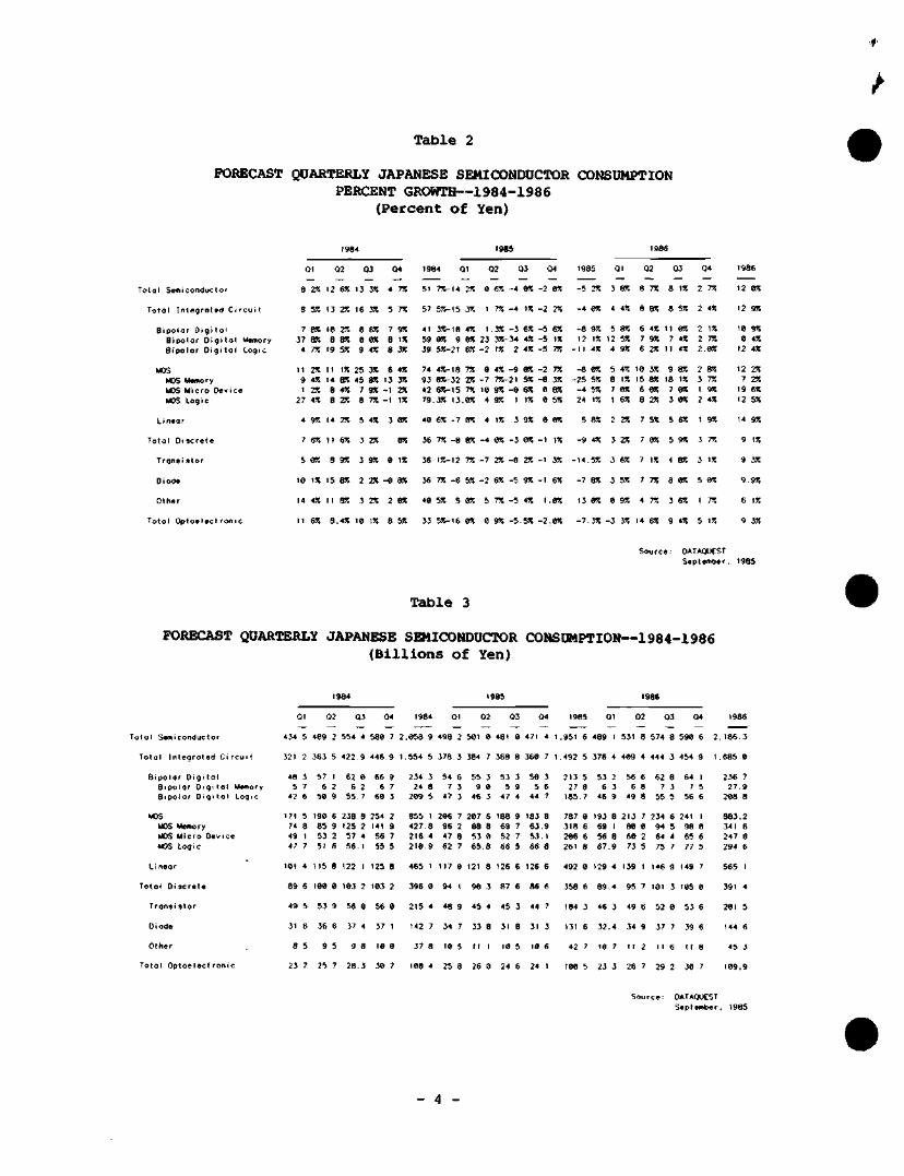
Table 2
FORECAST QUARTERLY JAPANESE SEMICONDUCTOR CONSUMPTION PERCENT GROWTH—1984-1986
(Percen t o f Yen)
Total Semiconductor
Total Integrated Circuit
Bipolar Digital
Bipolar Digital Memory
Bipolar Digital Logic
MOS MOS Memory
MOS Micro Device
MOS Logic
Linear
Totol Discrete
Transi 9tor
Diode
Other
Totol Optoelectronic
01
a
8
7 37 4
11 9 1
27
4
7
5
10
14
II
25!
57.
BX 87! 7%
27. *7.
7% 4%
917.
65!
8!!
IX
*7.
67.
02
12
13
18 8 19
11 14 8 8
14
11
8
15
11
8
65!
2r.
7% 8X 5!!
1!! 85! 45! 25!
25!
6%
9X
85!
85!
,4!!
03
13
16
8 8 9
25 45 7 8
5
3
3
2
3
10
35!
35!
65! 05! *7.
17. 85! 95E 75!
45!
25!
95!
25!
25!
15!
04
4
5
7 8 8
6 13 -1 -1
3
0
-8
2
8
7!!
75!
95! IX ST.
*7. 3X TT. 15!
85!
0X
IX
8X
8X
5X
1984 Ql
51
57
41 59 39
74 93 42 79.
48
36
36
36
48
33
75!-14 25!
5X-15 3X
35!-l8 4X
0X 9 8X
5X-21 6X
4X-18 7X 855-32 25!
6X-15 7X
3X 13.ax
6X -7 8X
7X -8 8X
IX-12 7X
7X -6 5X
5X 5 8X
5 V 1 6 8X
02
0
1
1 23 -2
8 -7 18 4
4
-4
-7
-2
5
0
6X
75!
.3X 3X-IX
4X 7X-9X 9X
IX
0X
2X
6X
75!
9X
03
-4
-4
-3 34 2
-9 21 -8 1
3
-3
-0
-5
-5
-5
8X
IX
ex 4X 4X
ax 5X
ex IX
9X
0X
2X
9X
4X
5X
04
-2
-2
-5 -5 -5
-2 -8 0 0
8
-1
-1
-1
1
-2
0X
2X
6X IX 7X
75! 3X SX 5X
0X
IX
3X
6X
,0X
,0X
1985
-5
-4
-8 12
-11
-8 -25 -4 24
5
-9
-14
-7
13
-7
2X
0X
9X IX 4X
BX 5X 5X IX
8X
4X
5X
8X
8X
3X
01
3
4
5 12 4
5 8 7 1
2
3
3
3
B
-3
8X
4X
8X SX 9X
4X IX 0X
ex 2X
2X
6X
5X
9X
3X
02
8
8
6 7 6
10 15 6 8
7
7
7
7
4
14
7X
8X
4X 9X 2X
3X 8X
ex 2X
5X
0X
IX
7X
7X
65!
03
8
8
11 7 11
9 18 7 3
5
5
4
8
3
9
IX
5X
0X 4X 4X
8X IX
ex ex 6X
9X
SX
ex
ex
4X
04
2
2
2 2 2
2 3 1 2
1
3
3
5
1
5
7X
4X
IX 7X
ex 8X 7X 9X 4X
9X
7X
IX
0X
7X
IX
1986
12 8X
12 9X
10 9X
0 4X
12 4X
12 2X
7 25!
19 ex 12 5X
14 9X
9 IX
9 3X
9.9X
6 IX
9 3X
Source: DATAQUtST
September. 1985
Table 3
FORECAST QUARTERLY JAPANESE SEMICONDUCTOR CONSUMPTION—1984-1986 ( B i l l i o n s o f Yen)
1984 1985 1996
Total Semiconductor
Total Integrated Circuit
Bipolor Digitol
Bipolar Oigitol Memory
Bipolor Digital Logic
MOS MOS Memory
MOS Micro Dev ice
MOS Logic
Linear
Total Discrete
Transi stor
Diode
Other
Total Optoelectronic
01 02 QJ 04 1984 01 02 03 04 1985 01 02 03
434 5 489 2 554 4 580 7 2.058 9 498 2 501 B 481 a 471 4 1,951 6 489 1 531 8 574 8
321 2 363 5 422.9 446 9 1,554 5 378 3 384 7 368 8 368 7 1,492 5 376 4 489 4 444 3
48 3 57 1 62 0 66 9 5 7 6 2 6 2 6 7
42 6 58 9 55 .7 60 3
171 5 198 6 238 8 254 2
74 8 85 9 125 2 141 9
49 1 53 2 57 4 56 7
4 7 7 5 1 6 56.1 55 5
lei 4 115 8 122 I 125 8
89 6 100 0 183 2 103 2
49 5 53 9 56 0 56 8
31 6 36 6 57 4 37 1
8 5 9 5 9 8 18 a
23 7 25 7 28.3 30 7
234 3 54 6 55 3 53 3 SB 3 24 8 7 3 9 8 5 9 5 6 209 5 47 3 46 3 47 4 44 7
855 1 206 7 287 6 188 9 183 8 427 8 96 2 88 8 69 7 63 9 216 4 47 8 53 8 52 7 53 1 218 9 62 7 65.8 66 5 66 8
465 1 117 0 121 8 126 6 126 6
396 0 94 I 98 3 87 6 86 6
215 4 48 9 45 4 45 3 44 7
142 7 34 7 33 8 31 8 31 3
37 8 18 5 111 10 5 18 6
108 4 25 8 26 8 24 6 24 1
213 5 53 2 56 e 62 8 27 8 6 3 6 8 7 3 185 7 46 9 49 8 55 5
787 0 193 8 213 7 234 6 318 6 69 1 88 8 94 5 286 6 56 8 68 2 64 4 261 8 67 9 73 5 75 7
492 0 129 4 139 1 146 9
358 6 89 4 95 7 181 3
184 3 46 3 49 6 52 0
131 6 32,4 34 9 37 7
42 7 10 7 112 116
108 5 23 3 26 7 29 2
04
598 6
454 9
64 1 7 5
56 6
241 1 98 0 65 6 77 5
149 7
105 0
53 6
39 6
1 1 8
30 7
1986
2.186.3
1.685 0
236 7 27 9 208 8
883.2 341 6 247 0 294 6
565 1
391 4
281 5
144 6
45 3
109.9
Source: DATAQUEST September. 1985
- 4 -
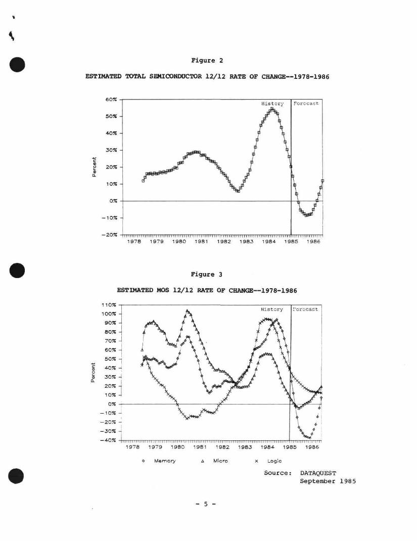
Figure 2
ESTIMATED TOTAL SEMICONDUCTOR 12/12 RATE OF CHANGE—1978-1986
c 0) o u 9>
Q.
6 0 %
50% -
4-0% -
3 0 % -
2 0 %
10% -
•10% -
-20% -|TrrnirnTrmTTTTT[TniTTT|[iniiiiT
Dataquest JAPANESE RESEARCH NEWSLETTER
JSIS Code: JSIA Newsletters
JAPANESE SEMICONDUCTOR MARKET UPDATE
DATAQUEST has revised its forecast for Japanese semiconductor consumption in 1985 and 1986 based on recent events that suggest a more prolonged downturn than originally foreseen. Table 1 shows a comparison of this forecast and our previous forecast of June 18, 1985.
One of 1985's major growth markets for both Japanese-made semiconductors and Japanese-made end equipment, such as televisions and refrigerators, has been the People's Republic of China. However, recent government restrictions and a lack of foreign currency have caused cancellation of orders in the second half of 1985. Many Japanese electronics firms were hard hit by the change in policy, which has certainly contributed to the current depressed state of the Japanese market.
Because of Japan's preeminence in consumer electronics, the Japanese semiconductor market is not as dependent on the ups and downs of the computer marketplace as the U.S. semiconductor market is. Thus, while the U.S. market is expected to decline 31.4 percent in 1985 and to grow 9.8 percent in 1986, the Japanese market will decline only 5.2 percent in 1985 and grow 12.0 percent in 1986 (yen basis). This huge delta in growth rates between the two countries means that by the end of 1986, the Japanese market will have grown to 33.9 percent of the world market, up from 30.1 percent in 1984.
Figure 1 shows our estimates of the quarter-to-quarter percentage changes in Japanese semiconductor consumption from 1984 through 1986. Although the second quarter of this year was up a scant 0.6 percent, we believe that the third and fourth quarters will show negative growth. We do not expect shipments to pick up until the first quarter of 1986.
Table 2 shows our quarterly growth forecast for the Japanese market through 1986. MOS memory is clearly the hardest hit product line this year, but it will show good recovery in 1986. Linear ICs and MOS logic devices will show positive growth this year, continuing into 1986.
Table 3 shows actual market values in yen for the same period as Table 1.
1985 Dataquest Incorporated Sept. 23 ed.-Reproduction Prohibited
The content of this report represents our interpretaion and anaIysis of information generally availabIe to the pubIic or reIeased by responsibIe individuals in the subject companies, but is not guaranteed as to accuracy or compIeteness It does not contain material provided to us in confidence by our clients Individual companies reported on and analyzed by DATAQUEST, may be clients of this and/or other DATAQUEST services This information is not furnished in connection with a sale or offer to sell securities or in connection with the solicitation of an offer to buy securities This firm and its parent and/or their officers, stockholders, or members of their families may, from time to time, have a long or short position in the securities mentioned and may sell or buy such securities
Azabu Heights, Suite 711, 1-5-10 Roppongi, Minato-ku, Tokyo 106, Japan 1290 Ridder Park Drive / San Jose, CA 95131 / (408) 971-9000 / Telex 171973

J
Figures 2 and 3 are 12/12 rate-of-change graphs. They are graphs of the percentage change of a moving 12-month total from the total for the same 12 months one year earlier. The resulting graphs show a smooth picture of the rate of change for a given product line.
Figure 2 shows historical and forecast rates of change for total semiconductor consumption. The point at which the line crosses the X axis in December of each year is the yearly growth rate for that year. We estimate that this point will be -5.2 percent in December 1985. By December 1986, however, the rate of change is expected to reach 12.0 percent.
Figure 3 shows historical and forecast rates of change for MOS memory, MOS micro devices, and MOS logic. As shown, the growth rate for MOS memory is falling precipitously from 91.1 percent in December 1984 to an anticipated -25.5 percent in December 1985. We believe that the turn in rate of change will occur in the second quarter of 1986.
Patricia S. Cox Gene Norrett
- 2 -
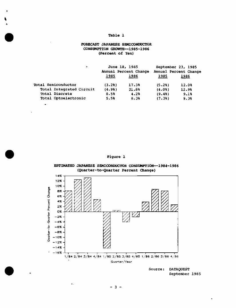
Table 1
FORECAST JAPANESE SEMICONDUCTOR CONSUMPTION GROWTH—1985-1986
(Percent of Yen)
Total Semiconductor Total Integrated Circuit Total Discrete Total Optoelectronic
June 18, 1985 Annual Percent Change 1985 1986
September 23, 1985 Annual Percent Change 1985 1986
(3.2%) (4.9%) 0.5% 5.5%
17.3% 21.8%
4.2% 8.3%
(5.2%) (4.0%) (9.4%) (7.3%)
12.0% 12.9%
9.1% 9.3%
F igure 1
ESTIMATED JAPANESE SEMICONDUCTOR CONSUMPTION—1984-1986 (Quarter - to -Quarter P e r c e n t Ctiange)
14%
Ol c o
X
o .._, c (U o 5) n
o t a D
a 0
L.
t : o or
125S
10%
8%
6%
4%
2%
0%
- 2 %
- 4 %
- 6 %
- 8 %
- 1 0 %
- 1 2 %
- 1 4 %
- 1 6 %
/ /
^
CA
m
/y
^ // / . 2
T \ 1 T 1 r 1 1 1 1 r 1 —
1/84 2 / 8 4 3 / 8 4 4 /84 1/85 2 / 8 5 3 / 8 5 4 / 8 5 1/86 2 /86 3 /86 4 / 8 6
Quarter/Year
Source: DATAQUEST September 1985
- 3 -

Table 2
FORECAST QUARTERLY JAPANESE SEMICONDUCTOR CONSUMPTION PERCENT GROWTH—1984-1986
(Percen t o f Yen)
,
Total Semiconductor
Total Integrated Circuit
Bipolar Digital Bipolar Digital Memory Bipolar Digital Logic
MOS MOS Memory MOS Micro Device MOS Logic
Linear
Total Discrete
Tronsi stor
Diode
Other
Total Optoelectronic
01
8
8
7 37 4
11 9 1
27
4
7
5
18
14
It
17.
ST.
ST. BK 77,
25! 4J! 2J! tr.
9)5
6%
m
15!
4r.
BX
02
12
13
18 6 19
11 14 8 8
14
11
8
15
11
S
6!I
2!!
25! 85! 57.
\Z 87. tx 27.
27.
6X
9%
ar.
85!
45!
03
13
16
8 8 9
25 45 7 8
5
3
3
2
3
18
i7.
i7.
65!
m 45!
35! 85! 95! 7X
45!
25!
95!
27.
27.
\7,
04
4
5
7 8 8
6 13 -1 -1
3
8
-e
2
8
75!
75!
9X 15! 35!
45! 37. 25! IX
85!
85!
\7.
35!
W.
5S
1984 01
51
57
41 59 39
74 93 42 79
48
36
36
36
48
33
7S-14
5r.-15
3^18 85! 9 5!!-21
4SH8 851-32
65H5 35! 13
65! -7
77. -8
155-12
75! -6
5r. 5
551-16
25!
3!!
45! 85! 65!
7X 25! 7X 85!
01?
85!
75!
5X
85!
017.
02
8
1
1 23 -2
8 -7 18 4
4
-4
-7
-2
5
e
ST.
75!
3!! 3V 1!!
45! 75!-
95! 95!
115
85!
251
651
75!
95!
03
-4
-4
-3 34 2
-9 21 -0 1
3
-3
-9
-5
-5
-5
85!
15!
ST. 45! V7.
97. 57.
en }7.
95!
m
77.
95!
4X
.55!
04
-2
-2
-5 -5 -5
-2 -8 8 8
8
-1
-1
-1
1
-2
85!
25!
65! IX 75!
75! 35! 8K 55!
ex
IX
3X
6X
ex
ex
1985
-5
-4
-8 12
-It
-8 -25 -4 24
5
-9
-14
-7
13
-7
2X
ex
9X IX 4X
8X 5X 5X IX
BX
4X
5X
8X
ex
3X
01
3
4
5 12 4
5 8 7 1
2
3
3
3
8
-3
8X
4X
8X 5X 9X
4X IX
ex 6X
2X
2X
6X
5X
9X
3X
02
8
8
6 7 6
18 15 6 8
7
7
7
7
4
14
7X
8X
4X 9X 2X
3X 8X
ex .25!
5X
ex
IX
7X
7X
6X
03
8
8
1 1
7 11
9 18 7 3
5
5
4
8
3
9
IX
5X
ex 4X 4X
8X tx
ex ex 6X
9X
8X
ex
6X
4X
04
2
2
Z •!.
2
2 i 1 1
1
3
3
5
1
5
7X
. 4X
IX 7X
ex 8X 7X 9X 4X
9X
7X
IX
ex
7X
IX
1986
12 ex
12 9X
18 9X 8 4X 12 4X
12 2X 7 2X 19 6X 12 5X
14 9X
9 IX
9.3X
9.9X
6 IX
9 3X
Source: DATAQUEST September. 1985
Table 3
FORECAST QUARTERLY JAPANESE SEMICONDUCTOR CONSUMPTION—1984-1986 ( B i l l i o n s o f Yen)
I 984 1985 1986
Total Semiconductor
Total Integroted Circuit
Bipolar Digital Bipolor Digitol Memory Bipolar Digital Logic
MOS MOS Memory MOS Micro Devi ce MOS Logic
Lineor
Total Discrete
Transistor
Diode
Other
Total Optoelectronic
01 02 03 04 1984 01 02 03 04 1985 01 02 03
434 5 489 2 554 4 588 7 2,858 9 498 2 581 8 481 8 471 4 1.951 6 489 1 531 8 574 8
321 2 363 5 422 9 446 9 1,554.5 378 3 384 7 368 8 368 7 1,492 5 376 4 499.4 444 3
48 3 57 1 62 8 66 9 5 7 6 2 6 2 6 7 42 6 58 9 55 7 68 3
234 3 54 6 55 3 53 3 58 3 24 8 7 3 9 8 5 9 5 6 289 5 47 3 46 3 47 4 44 7
213 5 53 2 56 6 62 8 27 B 6.3 6 8 7 3 185 7 46 9 49 8 55 5
171 5 19e 6 238 8 254 2 855 1 286 7 207 6 188 9 183 8 787 8 193 8 213 7 234 6 74 8 85 9 125 2 141 9 427 8 96 2 88 8 69 7 63,9 318 6 69 1 88 8 94 5 49 1 53 2 57 4 56 7 216 4 47 8 53 8 52 7 53 1 286 6 56 8 68 2 64 4 47 7 51 6 56 1 55 5 218 9 62 7 65.8 66 5 66 8 261 8 67 9 73 5 75 7
191 4 1 15 8 122 I 125 8
89 6 lee 8 183 2 183 2
49 5 53 9 56 8 56 8
31 6 36 6 37 4 37 1
8 5 9 5 9 8 18 8
23 7 25 7 28 3 38 7
465 1 117 8 121 8 126 6 126 6 492 8 129 4 139 1 146 9
396 e 94 1 98 3 87 6 86 6 358 6 89 4 95 7 181 3
215 4 48 9 45 4 45 3 44 7 184 3 46 3 49 6 52 8
142 7 34 7 33 8 31 8 31.3 131 6 32 4 34 9 37 7
37 8 18 5 111 le 5 10 6 42 7 18 7 112 116
188 4 25 8 26 9 24 6 24 1 188 5 23 3 26 7 29 2
04
590 6
464 9
64 1 7 5
56 6
241 1 98 8 65 6 77 5
149 7
185 8
53 6
39 6
1 1 8
38 7
1986
2,186 3
1.685 e
236 7 27 9 288 8
883 2 341 6 247 8 294 6
565 1
391 4
201.5
144 6
45 3
109 9
Source: DATAQUEST September, t9fl5
- 4 -

Figure 2
ESTIMATED TOTAL SEMICONDUCTOR 12/12 RATE OF CHANGE—1978-1986
6 0 %
5 0 % -
40%
3 0 %
P 2 0 % -v Q.
10%
•10% -
-20% i i i t i i i r i i i i i i I i i i I in i i Im INi Im I iHi i i in I i i i I i I i i i i i i in i i i i i i i i I i i r i i i i ' r i i i i rn i i I Ihi I r iTr i i I i i in i 1 9 7 8 1 9 7 9 1 9 8 0 1981 1 9 8 2 1 9 8 3 1 9 8 4 1 9 8 5 1 9 8 6
Figure 3
ESTIMATED MOS 12/12 BATE OF CHANGE~1978-1986
1 10%
1 0 0 % -
9 0 % -
8 0 % -
70% -
60% -
50% -
I 40% -i a '•
o 30% 4 1
20%
• 10% -i
0% ? J - 1 0 %
- 2 0 % -^
- 3 0 % -
- 4 0 %
H i s t o r y ror : ;caEt
i H i n n r i i i M H i v i T m i i I I I n i r n I i i i I i i i i i i i i f I i i I I i i i I i I i I i n i i i n i i i i in iM jn i r iT tnn 1978 1979 1980 1981 1982 1983 1984 1985 1986
<> M e m o r y A Micro x Logic
Source: DATAQUEST September 1985
- 5 -

Dataquest RESEARCH BULLETIN
JSIS Code: JSIA Newsletters
TURNING THE TIDE: U.S. SEMICONDUCTOR ACTIVITIES IN ASIA
The media has bombarded us in recent months with news about the demise of the U.S. semiconductor industry in the face of the Japanese and Korean challenges. How valid is this view? Are American makers destined to gradually decline? DATAQUEST believes that much of this reporting is sensationalism based on old ,news—the excellent sales achieved by Japanese companies in 1984. However, with the collapse of the computer market, we note that Japanese semiconductor makers are losing share in the ttiited States (see our trade update newsletter of July 10). Sales of MOB memory products, which accounted for 62 percent of total Japanese semiconductor exports to the United States in 1984, dropped 22 percent in the first half of 1985.
Moreover, we see signs of a serious effort by American makers to increase their presence in the Japanese market, as shown in Table 1. We believe that the following recent activities are significant:
•: IBM's staffing up of its Tokyo office, its entry into the value-added network (VAN) market with Mitsubishi, and its patent licensing agreement with MITI
• Nihon LSI Logic's tie-up with Kawasaki Steel to enter the gate array and standard cell market
• New Japanese plants announced by Analog Devices, Fairchild, Monsanto, Motorola, and National Semiconductor
# Opening of new design centers in Tokyo by AMI, GE Semiconductor, ITT Semiconductor, National Semiconductor, Nissec Fairchild, and Syntek
* New investments in Taiwan by Mosel, Motorola, Syntek, Unicorn Microelectronics, and Vitelic
© 1985 Dataquest Incorporated Sept. 5 ed.-Reproduction Prohibited
Tne
C'ov
* i l N
c o n l e n i o l ihis -eoorl .ep-e.sems our ,
. l e i l l o u s . n c o n l . d e n c e D y o u r r l . e m s
1 tm *_-• ^11 ^.w ill tf2 u LP«I I-.' t i 1^ 1 nf ,
lefpr
ndiv.r
•'•'*
tal ion an-l jna lys is of
ual compdi ies reporle
1ll|^ '.!!»• J/1L' I t l tJhT*^
n iofn ia l 'on qeneraliy available -f I K I . pu
JO'i and aiiaIy.-ed by DATAQUEST may ti
#nJ.L. r i t d i r ^V l i i ; * ' ! i iU ( l * f i rM j i t i i ' l ^ i'
)!:( O-
e U i c n
lllnih.l
(.,p ise
s o l ! • ,.. 0 0
or.siblp mdividuais .
•jli^er DATAQUEST s
• ' • ' " •
ihe sub
e'vices
iriir hti-'t
h.^ in lormabo
i iLirniui shtLi
bu, IS n,
n i s n o M L
jjULil'iLn
' Cjl
n i s
J-dOl
f d in
t i « i ;
ea as to accuracy o ' compleieness It does not conlain
connection « i lh a sale or otter lo sell securit ies or in con
HiJi*^rimMii(irLfU H^U mftj IffU nr Ciu» ^ U t n t r i t i j i i l i f l n
naierial
neclion
Dataquest Incorporated, A Subsidiary of A.C. Nielsen Company / 1290 Bidder Park Drive / San Jose, CA 95131 / (408) 971-9000 / Telex 171973

DATAQUEST believes that these aggressive marketing and investment plans are crucial for American companies expanding their businesses or getting started in Asia. The irony is that recent announcements by Japanese companies to buy more U.S. products may benefit old-timers in Japan--ttiose with established long-term ties with Japanese customers— more than newcomers just setting up shop.
Sheridan Tatsuno
Table 1
U.S . SEMICONDUCTOR ACTIVITIES IN ASIA
Company Loca t ion A c t i v i t y
AMI Analog Devices AT&T General Electric
fiarris Semiconductor Hewlett-Packard High Technology Systems Corp. Hugle Electronics
IBM
Intel
Tokyo, Japan Kanagawa, Japan Tokyo, Japan Tokyo, Japan
Tokyo, Japan Tokyo, Japan
Tokyo, Japan Tokyo, Japan Korea Tokyo, Japan
Korea
ITT Semiconductors KLA Instruments
LSI Logic LTX Micron Technology Monsanto
Mosel Motorola
National Semiconductor NCR Nissec Fairchild
Perkin-Elmer Syntek Texas Instruments Unicorn Microelectronics Vitelic
Tokyo, Japan Tokyo, Japan
Tokyo, Japan Tokyo, Japan Tokyo, Japan Utsunomiya, Japan
Taiwan Taiwan
Aizu, Japan
Taiwan Tokyo, Japan Nagasaki, Japan Tokyo, Japan
Tokyo, Japan Taiwan Tsukuba, Japan
Taiwan Taiwan
Wafer Scale Integration Tokyo, Japan
Design center with Asahi Chemical New building and IC plant in 1987 VAN consortium with 18 companies New company (GE Semiconductor) and gate array design center Sales agreement with Internix Subsidiary (Harris Corp.) Procurement office Joint sputtering equipment production with Anelva Corp. Wafer cassette plant with Atcor Joint venture with Zeus Corp. Japanese government patent license
Samsung manufacturing agreement and new branches in Korea and Taiwan LSI design center New company (LA Technology Center) Nihon LSI/Kawasaki Steel tie-up Plant acquisition for IC testers Direct sales office Silicon wafer plant and R&D center 1.5-micron VLSI plant $100 million electronic components plant New VLSI plant
VLSI logic array design center Pull-scale sales program 1- to 2-micron CMOS pilot line CMOS and ECL gate array design center Sales and service group Design center in Hsinchu Park ULSI plant at Expo 85 site
United Microelectronics funds Wafer fab contract with ERSO; ties with Sony and Kyocera
Joint development of 1Mb CMOS DRAM with Taiwan government
Wafers from Sharp
Source: DATAQUEST
- 2 -

Dataquest JAPANESE RESEARCH NEWSLETTER
JSIA Code: Newsletters
JAPANESE SEMICONDDCTOR TECHiaOLOGY TRENDS Second Quarter 1985
SUMMARY
Despite ttie severe industry downturn, the outpouring of new Japanese technologies and products is accelerating. During the second quarter, DATAQUEST observed a rapid shift from commodity items to application-specific memories (ASMs), original MPUs/MCUs, gate arrays, standard cells, and optically based sensors and ICs. New applications are also being pursued, such as IC memory cards, 8mm video cameras, high-definition and sound multiplex televisions, facsimiles, medical diagnostic tools^ optical communications, voice synthesis/recognition, graphics and television displays, and laser printers. We also note that MITI's 10-year joint R&D projects are half way through completion and spinning off new technologies.
DATAQUEST believes that the following semiconductor technology are significant.
developments in Japanese
Basic Research
• Opening of new corporate R&D centers (NEC, Tokyo Sanyo, TDK)
• MITI's planned new synthetic diamond substrate joint R&D project
• Expansion of the installed base of supercomputers
• Progress in 3-dimensional ICs and superlattices at MITI's Itew Function Elements Project (1981-1990)
New Products and Device Technologies
• Sampling of 1Mb DRAMs (Fujitsu, Hitachi, Oki, and Toshiba)
• Introduction of high-speed bipolar CMOS (Hi-Bi-CMOS) 64K SRAMs (Hitachi) and gate arrays (Toshiba)
for
© 1985 Dataquest Incorporated Aug. 16 ed.-Reproduction Prohibited
The content of this report represents our interpretaion and analysis of information generally available to the public or released by responsible individuals in the subject companies, but is not guaranteed as to accuracy or completeness It does not contain material provided to us in confidence by our clients Individual companies reported on and analyzed by DATAQUEST, may be clients of this and/or other DATAOUEST services This information is not furnished in connection with a sale or offer to sell securities or in connection with the solicitation of an offer to buy securities This firm and its parent and/or their officers, stockholders, or members of their families may, from time to time, have a long or short position in the securities mentioned and may sell or buy such securities
Azabu Heights, Suite 711, 1-5-10 Roppongi, MInato-ku, Tokyo 106, Japan 1290 Ridder Park Drive / San Jose, CA 95131 / (408) 971-9000 / Telex 171973

• Rapid growth in IC cards with MPUs, EPROMs, and EEPROMs for banking/ credit, and medical identificationr and for data processing (Kycjdo Printing, Mitsubishi, and Dai Nippon)
• Development of a three-level polysilicon structure for CMOS EEPROMs (Toshiba)
• Proliferation of original 8-bit and 16-bit CMOS MPUs and intense research on application-specific 16-bit MCU "superchips" (Hitachi, Japan Victor, Mitsubishi, and NEC)
• Introduction of a 3-D CMOS 16-bit MPU (Matsushita)
• Development work on 32-bit MPUs (Hitachi, NEC, and Oki)
• Marketing of a V20/V30 MPU development support system (Sony/ Tektronix)
• Development of digital signal processors (DSP) for television and graphics displays and speech recognition (Fujitsu, Hitachi, Mitsubishi, and NEC)
• Introduction of CMOS standard cell libraries (Asahi Microsystems, Fujitsu, Japan Victor, Matsushita, Mitsubishi, NEC, Ricoh, Sharp, Toshiba, and Yamaha)
•' Use of semiconductor lasers in car systems (Nissan); optical disks, television animation, audio, and video disks (NEC); copiers, printers, PCS, and OA equipment (Sharp)
• Use of CCD image sensors for video cameras, sound multiplex and high-definition televisions, facsimiles, copiers, and computer input (Fuji Photo Film, Matsushita, Mitsubishi, NEC, Olympus, TI Japan, and Toshiba)
• Development of GaAs logic ICs for high-speed multiplexed communication signals (Matsushita)
• Use of biosensors in medical diagnostic tools and artificial human organs (Matsushita); and bioelectronic research (NEC/MITI)
Equitwient, Materials, and Packaging
• An excimer laser photolithographic unit for 16Mb DRAMs and electron-beam littiography, and fog exposure technology for 64Mb-level DRAMs (Toshiba)
• New equipment for photomask correction (NEC); wafer particle detection (Hitachi); and fully automatic defect detection (NJS)
• Ultra high-speed electron beam testing (Hitachi)
#
- 2 -

• Zig-zag in-line packaging (ZIP) for 256K DRAMs (Fujitsu and Mitsubishi)
• Replacement of gold wire bonding with copper wire bonding (Mitsubishi) ,*
CORPORATE R&D LABS
NEC has establish a ¥10 billion ($40 million) R&D center within its Sagamihara Works near Tokyo to develop silicon wafers for next-generation ICs, such as 4Mb DRAMs and 32-bit MPUs. The center comprises 3/000 square meters of space and has highly sophisticated equipment.
Tokyo Sanyo Electric has announced plans to build a new R&D center and laboratory by next spring either in its main plant or in the VLSI plant in Niigata Sanyo Electric. The center will focus on 4Mb and higher VLSIs.
TDK Corporation/ the world's largest maker of ferrites and magnetic tapes with ¥178.8 billion (3715 million) in sales in 1984r announced that it will enter ttie semiconductor market. The company plans to build a Semiconductor Technology Technical Center in Saku/ Nagano Prefecture, by the end of this year. The two-storied ¥4.5 billion plant ($18 million) will produce thin-film magnetic heads for its hard disk drives. Its 200 to 300 researchers will focus on GaAs sensors, high-power transistors, and thermal printer drive ICs.
The Japanese government plays a major role in promoting joint research in next-generation semiconductors. EHiring the second quarter, the Ministry of International Trade and Industry (MITI) and Nippon Telegraph and Telephone (NTT) made the following announcements that we believe will greatly affect the semiconductor industry:
GOVERNMEMT R&D PROJECTS
Nippon Telegraph and Telephone's (NTT) Information Network System (INS)
NTT announced on May 21 that it will invest ¥1.66 trillion ($6.64 billion) in plant and equipment in fiscal 1985, including ¥480 billion (31.92 billion) in its nationwide Information Network System. DATAQUEST believes that in 1985, the semiconductor content of the telecommunications equipment procured by NTT will be approximately 12 percent, or $800 million. Of this amount, INS procurement will
- 3 -

account for $230 million. In fiscal 1984, NTT invested about ¥380 billion ($1.52 billion) in INS, of which we believe semiconductors accounted for about 11.5 percent, or $175 million. NTT is also increasing its R&D budget. In fiscal 1985, NTT plans to spend yl70 billion ($680 million) for basic research, which is about,six times the amount spent by the Ministry of International Trade and Industry (MITI) .
MITI New Diamond gorum
MITI recently held an inaugural meeting of the New Diamond Forum to discuss the possibility of using synthetic diamonds as substrates for future semiconductors. About 200 companies from the electronic, automotive, steel, and other industries are being sought to form a joint govertunent-industry R&D project and to secure budget support starting in fiscal 1987. MITI is attempting to catch up with the United States, which is currently using synthetic diamonds in space electronic equipnent. Materials with better heat resistance and thermal conductance are required for faster data processing speeds and extreme conditions, sucti as space, aviation, nuclear power plants, and automobile engines.
MITI Supercomputer Project (1981-1990)
Fujitsu.has added two supercomputers to its VP series. The high-end machine (VP400) executes 1.14 GFLOPS (billion floating-point operations per second) and has a maximum memory of 256 megabytes, 128 kilobytes of vector register, and 2,048-byte mask register. The entry-level machine (VP50) handles 140 MFLOPS (million floating-point operations per second) and offers a 128-megabyte maximum memory, a 32-kilobyte vector register, and a 512-byte mask register. Both machines have 64 kilobytes of buffer storage, a maximum of 32 channels, and a maximum transfer speed of 96 megabytes per second. They are compatible with IBM's M series mainframes and can perform vector processing. The VP400 will be delivered starting in December and leased at V79 million ($322,450) per month. The VP50 will be shipped in September and leased at ¥46,000 ($184,000) per month. DATAQUEST observes that the VP400 is competitive with NEC's SX2 (1.3 GFLOPS), the Cray 2 (2.0 GFLOPS), and Hitachi's S810 (630 MFLOPS).
Supercomputer makers are gradually increasing their installed base in Japan. DATAQUEST notes that several companies and research centers have purchased or are planning to purchase a supercomputer, as shown in Table 1.
- 4 -

Table 1
RECENT SUPERCOMPUTER PURCHASES IN JAPAN
Computer Malcer
Cray Research
Fujitsu
Model
Cray 1
Cray X-MP
VPIOO
Hitachi S810 SX-2
Purchaser
Mitsubishi Central Research Lab Toshiba Research Lab Nippon Telegraph and Telephone
Nissan Motor Company (36.5 million; planned)
Nagoya University Plasma Research Lab Kyoto University Data Processing Center Japan Nuclear Research Lab Power Generation & Nuclear Fuel Development Agency Toyota Motors (planned)
Tokyo University Data Processing Center Osaka University
Source: DATAQUEST
MITI New Semiconductor Function Elements Project (1981-1990)
On June 28, Shigeru Fukuda, a Fujitsu employee and current manager of MITI's superlattice research, gave a presentation at DATAQUEST on the status of the New Function Elements Project. DATAQUEST believes this is MITI's VLSI Project for the 1980s, which will introduce next-generation technologies, including 3-dimensional ICs, superlattice devices (silicon and GaAs), and hardened ICs. Due to national budget deficits, the project is only budgeted for Vl.2 billion ($4.5 million) in fiscal 1985, half the originally scheduled amount. Nevertheless, the member companies are increasing their R&D spending in these areas. We will issue a special newsletter examining the progress of this important project.
To date, the project has generated 373 papers and 282 patents (pending), as shown in Tables 2 and 3, respectively.
Almost two-thirds of the papers and pending patents in Tables 2 and 3 are for 3-dimensional ICs. When asked about this trend, the previous research manager, Mr. Kawashima, explained that MITI has decided to focus its efforts on 3-D ICs, where it believes Japan has a two-year lead over the West. In contrast, he noted that Japan is about six to seven years behind in hardened iCs, and is about equal in superlattices. In addition to developing new "bargaining chips" to trade with the West, DATAQUEST
- 5 -

believes that MITI has chosen the 3-D IC' because of its immediate applications to 4Mb and 16Mb DRAM research. New 3-D technology will enable Japanese companies to develop faster memory and logic chips using the new configurations.
Table 2
MITI NEN FUNCTION ELEMENTS PROJECT (Technical Papers)
Fiscal Year
1981 1982 1983 1984
Superlattice Devices
1 11 31 33
3-Dimensional ICs
6 53 86 85
Hardened ICs
• 0
18 30 19
Total
7 82 147 137
Total 176 230 67 373
Table 3
NEN SEMICONDUCTOR FtmCTION ELEMENTS PROJECT (Patents Pending Under Contract)
Fiscal Year
1981 1982 1983 1984
Superlattice Devices
1 6 16
• 10
3-Dimensional ICs
6 64 75 74
Hardened ICs
1 10 12 7
Total
8 80 103 91
Total 33 219 30 282
Source: DATAQUEST
- 6 -

MiTI's Institute of Industrial Technology
The Institute of Industrial Technology recently unveiled a prototype reading machine that automatically turns pages, reads books in Japanese, and vocalizes the words synthetically. The system consists of a robot manipulator page turner linked to an optical character reader. MITI plans to develop a commercially viable machine by 1988 for use by the blind and handicapped. The price will be about ¥30 million ($120,000). DATAQUEST believes that a limited market for optical sensors and voice synthesis chips will develop around this product.
NEW PR0DIX:TS AND TECHNOIOGY TRENDS
In past newsletters, DATAQUEST reported technology trends (advanced research and prototype development) and new products announcements in separate sections. Beginning with this newsletter, we will combine the two sections Into a single New Products and Technology Trends section. To monitor Japanese trends, we use the following rule of thumb: Japanese technical papers generally precede prototype devices by 12 to 18 months, product samples by 24 months, and mass production by 30 to 36 months, depending upon the market demand.
Memory
Although production of 256K DRAMs has just begun, Japanese makers have announced that they will begin sampling 1Mb DRAMs. By the end of 1985, DATAQUEST believes that Fujitsu, Hitachi, Oki, and Toshiba will begin sampling, while NEC will take a more prudent stance by not preceding these makers. Matsushita and Mitsubishi will start sample shi Hnents in early 1986.
• Fujitsu—256K DRAMs in zig-zag in-line package (ZIP) and PLCC packages; access times of 100/120/150ns; sample prices of ¥3,700 ($14.80) for ZIP devices and ¥3,500 ($14) for PLCC devices
• Gold Star—Plans to sample 64K CMOS SRAMs starting in August
• Hitachi—A high-speed bipolar-CMOS (HiBiCMOS) 64K SRAM (IM6787) with ECL speeds and CMOS low-power consumption; 25ns access time; 220mW power consumption during operation and 16mA driving output power; TTL-compatible; 8.5x3.4mm; 22-pin CERDIP package 22-pin 300-mil ceramic DIP; sampling price of ¥15,000 ($60), or ¥8,000 ($32) for lots of 1,000; monthly production of 300,000 to 500,000 units
Six CMOS 256K SRAM models; general types and battery backup type; 85/100/120ns access times; 1.3-micron rule; 1.6 million transistors on a 4.98x9.4mm chip; shipments in June; sample prices between ¥15,000 ($60) and ¥22,000 ($88); monthly production of 200,000 by late 1985
- 7 -

A CMOS 256K EPROM with low program voltage of 12.5 volts (HN27C256) ; access times of 200/250/300ns; 200ns device sampling at ¥5,000 ($20) for orders of 10/000; developed using polysilicon EMOS technology
Two CMOS 256K SRAM versions, one with battery backup, and three access times (85/100/120ns); 28-pin plastic DIP packages
Sampling of 1Mb DRAMs; static column CMOS type; 4.66xl0.1mm
A 64K SRAM in a 300-mil slim-line package (HM6264ASP); access times Of 120/150ns; power dissipation of 15mW during operation and lOmW at standby; 8,192x8-bit parts sampling at ¥4,000 ($16)
A prototype 16Mb magnetic bubble memory developed using ion implant technology; conventional Permalloy transfer circuit and ion implanter circuit combined on the chip; commercialization planned for mid-1986, witti 64Mb model by 1989
Matsushita—An 8-bit content-addressable memory (CAM) for use in non-Neumann logic computers; 30x36-inicron device with 3-layer blocks for checking data block by block; 236x32-bit memory structure; 99,000 transistor equivalent
TWO NMOS 128K DRAMs using 2-micron silicon gate process; 128Kxl-bit structure; chip size of 3.8 x 5.16mm; 16-pin DIL package; access time of 120ns (MN41128-12) and 150ns (MN41128-15); priced at ¥550 ($2.20); monthly production of 50,000 units to be increased to 500,000 units by late 1985; Zig zag in-line package (ZIP) and PLCC
Mitsubishi—256K DRAMs in two package types; three access speeds and page or nibble mode available for each type; device in PLCC package one-third tiie size of DIP-mounted devices (M5M4256J) ; device in zig-zag in-line package (ZIP) using through-hole mounting (M5M4256L); PLCC versions priced at ¥5000 ($20) for 120ns, ¥4500 ($18) for 150ns, and ¥4000 ($16) for 200ns; ZIP devices priced at ¥3800 ($15.20) for 120ns, ¥3400 (13.60) for 150ns, and ¥3000 ($12) for 200ns
A NMOS 256K EPROM using 2-micron rule N-channel silicon gate process; 200/250/300ns access times; sample shipments in June; initial monthly production of 50,000 units; priced at ¥4,000 ($16)
A line Of 16K SRAMs (M5M21C67P) ; 16Kxl-bit and 4Kx4-bit types; 35/45/55ns access times; sample price of ¥2,000 ($8) for 35ns types
An NMOS silicon gate 1Mb ROM (M5M231000P) available in 250 and -300ns access times; 28-pin DIL plastic package; sample price of ¥6,000 ($24)
- 8 -

NEC—A pseudostatic 256K RAM combining NMOS and CMOS DRAM functions (uPD42832C); available in 100/120/150ns; 32Kx8-bit structure pin-compatible with similarly structured CMOS SRAMs; 4.6 X S.Omm; 28-pin DIP package; ¥6,000 ($24) sample price for 150ns type
Ricoti—A 256K CMOS EPROM with 12.5V write voltage and 150ns access time; 2-layer silicon with 1.5-micron pattern, with a sense circuit to accept wide voltage fluctuation; sample prices Of ¥4,000 ($16)
Toshiba—8 percent to 9 percent yields with free 1Mb DRAMs being given to a limited number of users; sampling expected when yields exceed 10 percent
A 64K CMOS EEPROM with 50ns access time; 1 transistor, 3-level polysilicon structure; 2-micron n-channel CMOS; 5.95x4.88mm chip; power consumption of 25mW during operation
Application-Specific ttemory (ASM)
• Dai Nippon Printing—An optical memory card with 422 kilobytes of storage capacity (160 pages of A4 size text); production cost about $1.20; priced at $20 to 40; enhancement of storage capacity to 2 megabytes possible with fine pattern drawing technology; data read-out only using CCD line sensors
• Fujitsu—^A hybirid device combining a 2,375-gate array and 1,024-bit SRAM on a 6.7x7.limn chip; 2.2ns delay time; four types (256x4/128x8/ 64x16/32x32)
• Kyodo Printing—16K, 64K, and 128K IC cards with EPROMs and EEPROMs in 16K and 64K capacities; two types of 8C card read-write machines for processing data
• Mitsubishi—Five types of IC memory smart cards; sample 1.8mm mask ROM card priced at ¥4,500 ($18); EPROM card with 8-bit MPU at ¥10,000 ($40); card with 8-bit MPU and 64K SRAM for computer data files at ¥15,000 ($60); an ISO-standard 0.75mm thick IC card with MPU and EPROM being developed for banking and credit uses
• NEC—A CMOS 2Mb mask ROM (uPD23C2000C) integrating 2.4 million elements and capable of storing 8,000 kanji characters; 6.63 X 8.42mm chip; 1.2-micron geometry; 250ns access time; power dissipation of 40 milliamperes during operation and 100 microamps at standby; 131,072 x 16-bit for word mode designation and 262,144 x 8-bit for byte mode; plastic or ceramic 40-pin 400 mil DIP; for use in portable Japanese language word processors, hand-held computers, and typewriters; priced at ¥8,000 ($32) each in lots of 1,000
- 9 -

Sharp—Four 1.2Mb CMOS kanji character generators (LH53012 series); suitable for CRT displays; I/O TTL-compatible; single +5V power supply; 3-state output; 40-pin plastic DIP; priced at ¥13,500 ($54)
Suwa Seikosha—A CMOS tone-pulse telephone dialing circuit; 10-extension, 18-digit repeat memory devices for telephone number storage and 24-digit redial memory capability; 20,000 devices per month piroduction
Microprocessors/Microcontrollers
• Fujitsu—Three NMOS and one CMOS one-chip MPUs with 256-word RAM capacity and power-on reset circuit; optional selection of 4-bit units; 4,096x8-bit ROM capacity
Sample shipments of 8-bit and 16-bit MPUs (80186/80188/ 80286) licensed from Intel
Two CMOS 4-bit MCUs added to a total of 14 series and 40 models; MB88201H with 0.5 Kbyte ROM and 16x4-bit RAM and MB88202H with 1 Kbyte ROM and 32x4-bit RAM; sample shipments at ¥230 ($0.92) and ¥280 ($1.12), respectively; also a low-price, general-purpose MCU with built-in A/D converter (MB88211) priced at ¥360 ($1.44) for 1,000-unit orders; initial monthly production of 200,000
• Hitachi—Two proprietary CMOS 8-bit MPUs with 4K EPROM and memory peripherals for the 6305 series; HD6505V mask ROM and HD6375V with 256K EPROM; 31 I/O ports, serial interface, and two timers; software-compatible and 192-byte RAM; minimum execution times of 0.5, 0.67, and Ins; 40-pin package
A CMOS 8-bit single-chip MPU with 4 Kbytes of mask ROM and EPROM (HD6305V) ; 54-pin flat package; 1.0/1.5/2.OMHz speed; wait mode lOmW; operating imsde 35mW; sample price of ¥1,500 ($6); also an 8-bit MCU with an EPROM (HD63705V); sample price of ¥8,000 ($32)
Two original 8-bit CMOS single-chip MCUs using a 40-pin package; one device with mask ROM (HD6305V) and another with an EPROM; 40-pin package
Three CMOS 8-bit MCUs (Zero Turnaround Time); plastic package; shipments from May at ¥2,000-¥3,800 ($8-15.20)
A real-time operating system for measurement and control systems using 16-bit MCUs; parallel program development possible by mounting CP/M-68K as a second operating system; 27 to 28 modules
- 10 -

Matsushita—An original 3-dimensional CMOS 16-bit MPU (MN1617) developed using silicon-gate/ 2-micron gate patterns, and 2-layer, 3-D aluminum wiring patterns; 200ns execution time with 200mW power consumption at 20 MHz; SOmW at standby; 64-pin flat package; priced at ¥10/000 (340); sales since June
An original NMOS silicon-gate, 8-bit MPU (MN18900) using 2.5-micron rule; parallel processing with two 8-bit microprocessors and timing based on paired,.16-bit timer counters; 51 I/O parts, 4K ROM, and 256-byte RAM; expandable to 64K; 500ns execution time; 64-pin, shrink DIP package
A series of OlOS 4-bit MCUs (MN1700 series); 2-micron silicon gate process; multiplication direction function with 1 microsecond direction cycle; MN1758 with 8K ROM and 512-word RAM sampling at ¥2,000 ($8); EP17516 piggyback type at ¥20,000 ($80); MN1799 evaluator with 16K ROM and 512-word RAM at ¥6,000 ($30)
A CRT controller (MN8355) with a built-in erasable RAM; transfer speed of 30ns/dot in monochrome and 500ns/pixel (16-bit gradation) in color; shipments starting in September; sample price of ¥20,000 ($80)
Mitsubishi—An 8-bit CMOS MPU incorporating an A/D converter, timer/event counter, and universal asynchronous receiver/ transmitter (M50734-SP); for use in electronic typewriters, hand-held computers, copiers, and electronic musical instruments; priced at ¥1,450 ($5.80); monthly production of 100,000
A flexible disk drive single-chip MCU (M52810FP) designed for portable computers; fabricated using Bi-CMOS wafer processing; SOmW power dissipation; sample price of ¥2,000 ($8) ; monthly production of 200,000 units
Plans for sample shipment of 16-bit MCU prototypes within one year; 32-bit MPU also being developed
NEC—A CMOS 16-bit direct-memory access (DMA) controller (UPD71071C); transmits data at 5.3Mb/sec at 8 MHz without an MPU; four separate DMA channels consisting of 5,000 elements; 2-micron; 16Mb of address space; capable of interfacing with 8-or 16-bit MPUs; four independent built-in DMA channels; monthly production of 50,000 doubling by late 1985
Sampling of CMOS 8-bit V40 (uPD70208) and CMOS 16-bit V50 (UPD70216) MPUs starting this summer; 68-pin leadless chip carrier; 4-channel CMA controller; DRAM refresh controller; 8-level controller; 16-bit timer/counter; programmable wait function; serial interface; 64 Kbyte I/O space
- 11 -

A CMOS flexible disk format controller (MB89311), which is compatible with NEC's NMOS flexible disk controller (MB8877A); sample shipnents in August; priced at ¥2,500 (310)
Two 4-bit CMOS MPUs with peripherals having the performance of 8-bit MPUs; 0.95-microsecond command execution time for the central processor; first of NEC's uCOMOS-75X series, including the UPDD75106CW with a 6K mask ROM and the uPD75Pl08DW with an 8K EPROM
• Oki Electric—An advanced 8-bit MCU (80C51) with 4Kx8-bit ROM and 128x8-bit RAM; 12-MHz operating frequency; capable of executing the same instruction set used with Intel's HMOS 8051; 111 instructions, including hardware multiply and divide; 32 I/O lines organized into four 8-bit ports; priced at ¥3,500 ($14); monthly production of 5OK to 10OK
Development of proprietary 32-bit MPU for introduction by late 1985; plans for captive use in minicomputers; second-sourcing agreements also being sought
• Sanyo—An NMOS 8-bit, single-chip MPU with built-in 8-bit bus interface for apparatus control (LM8854); 16K ROM; 2K RAM; 5V power supply; 64-pin shrink DIP; priced at ¥700 ($2.80)
• Sony—Three CMOS 4-bit MCU devices; a 64-pin, piggyback MCU (CXP5020) for debugging and evaluating; a general-purpose MCU (CXP5034) with 4K ROM and RAM structure; one MCU with an 8K external EPROM extension
Sony/Tektronix—NEC V20/V30 MPU development support system that can also handle Motorola 68010 and Intel 80186
Original 8-bit CMOS single-chip MCU planned for commercialization within one year; 4-bit MCU (SPC-5000 series) available since late 1984; second sourcing of NEC's 16-bit V20 and V30 MPUs
• Suwa Seikosha—4-bit and 8-bit CMOS, one-chip MCUs; 8-bit SMC8340F series with 4K ROM and 128 bytes of RAM; 4-bit SMC4040C MPUs with 512-byte ROM and 16x4-bit RAM
• Toshiba—A CMOS 4-bit MPU for handling truncated dialing and automatic redialing, vith a dual-time, multifrequency tone dialer; 38.2x14.2mm; 2K ROM and 256x4-bit ROM configuration for repeat dialing; 31 I/O ports; 42-pin shrink package
A real-time clock LSI (TC8250P) for constant time control; display timer and refresh for repeated image display at 1mA power consumption; 16-pin DIP package; ¥500 sample price (32); also a CRT controller LSI (TC8505P) with display timing and memory refresh for repeated image display
- 12 -

Digital Signal Processors (DSP)
t Fujitsu—Two CMOS high-efficiency television display controllers capable of controlling the display of 180 characters and symbols on CRTs; sample prices of ¥1,000 ($4.00) for 1,000-unit orders Of the MB88323 and ¥1,300 ($5.20) for the MB88324; shipments from late 1985
, • Hitachi—A bipolar CMOS digital signal processing R M with a LED and 280-bit SRAM; 400-MHz bipolar transistor; 80mA, 9-segment LED; 12.7V power voltage; 1,500 gates; 5-micron silicon gate CMOS; 5.0x5.5mm chip size
4 Matsushita—Two speech signal processors connected to a minicomputer; LPC analysis and 2-channel filter analysis performed by DSP-1; input parameter compared to phoneme standard pattern by DSP-2; calculations executed in real time
A graphics display control processor (MN8350) for CRTs and LCD displays; CMOS silicon gate; 2.0-micron process; shrink DIP and flat package; 10-MHz operating frequency; 300 mraW power consumption; sample price of ¥10,000 ($40); shipments from fall 1985
TWO high-function DSP LSis with twice the processing capacity as conventional models; MN1909 priced at ¥100,000 ($50); MN1901 with 8K built-in ROM priced at ¥5,000 ($20)
• NEC—^A high-performance LSI (uPD7764) for DP matching processes; NMOS chip with 40,000 devices for speech recognition template matching; 40-pin standard package; capable of matching about 300 discrete words and recognizing 30 connected words by two-level DP matching
/^plication-Specific ICs (ASICs)
• Fujitsu—A hybrid device combining a 2,375-gate array and 1,024-bit SRAM on a 6.7 x 7.1mm chip; 2.2ns delay; four arctiitectures (256x4/128x8/64x16/32x32) ; 13 package types up to 135-pin grid array; 2.3-micron rule for the SRAM portion
A standard cell library with 100 cells; CMOS parts with 2.1ns per gate delay time; orders accepted in Tokyo, Osaka, and Santa Clara; new design centers planned for Boston, Dallas, and Manchester, U.K.; recent standard cell entrants include Nippon Gakki (Yamaha), Asahi Microsystems, 'Doshiba, Sharp, NEC, Japan Victor (JVC), and Mitsubishi
• Hitachi—Six CMOS gate array products with from 448 to 2,560 gates; (HG61H Series); 2ns delay time; capable of mounting SRAMs; can be designed with Daisy and Mentor CAD workstations; $2.00 to $9.40 for 40-pin package devices in lots of 10,000
- 13 -
• Matsushita—An original standard cell CAD system capable of developing full-custom LSIs; cell library of 200 cells/ including various functional blocks of RAMs, ROMs, comparators, A/D and D/A converters
A new CAD program (SMILE) for automatic layout of 10,000-gate class LSIs within 6 minutes; layout time 1/5 to 1/20 of conventional methods due to new method of wiring and block arrangement; developed experimental DSP LSI for portable CD
• Mitsubishi—A 1,100-gate CMOS array using silicon-on-insulator (SOI) and laser recrystallization; 5.37 x 4.9mm prototype chip with 3,432 cells, 66 I/O buffers, and 7,524 transistors; 120ns operations on an 8 x 8 parallel multiplier section; 1.3ns delay per inverter stage with a no-load 19-stage. ring oscillator; 0.25mN power consumption; 0.8ns delay possible with 1.5-micron design rule
• NEC—A new CMOS gate array series of 8 models up to 20,000 gates; prices for arrays: development cost of ¥15.5 million ($62,000) for 20,000-.gate model priced at ¥36,000 ($144), ¥4.4 million ($17,600) for 2,100-gate model priced at Yl,700 ($6.80) for 10,000-unit orders, ¥9.4 million ($37,600) for 6,700-gate model priced at ¥5,400 ($21.60)
• Nippon Gakki (Yamaha)--Company goal of reducing standard cell development time to six weeks; turnaround time for 500-gate arrays about two weeks
• Sharp—Orders accepted for CMOS standard cell LSIs; four types (CMOS 1 to CMOS 4) ; plans to produce 500,000 units monttily
A standard cell correction program that allows changes in the position of elements even after wiring has begun; potential 10 percent reduction in chip size possible
• Toshiba—CMOS/SOS (silicon on sapphire) gate arrays for captive use; 8,370 gates and 35,000 devices on a 9.84x9.92mm chip; 0.75ns gate delay time; 300 imnW power consumption; also a 16xl6-bit multiplier with 11,500 devices on a 4.35x4.35mm chip; 30ns multiplication time; 250 mmW power consumption; multiplier priced at ¥50,000 ($200)
A triple-layer wiring program for standard cells that permits a 10 percent reduction in ctiip size
CAD Systems
• Fujitsu—A CAD system that completely automates logic circuit design using artificial intelligence (Al) technology; 200 complex design rules gathered from experts and input into computer's knowledge base
- 14 -

standard Logic
Fujitsu—High-speed CMOS standard logic ICs (MB74HC series); TTL-compatible; operating voltage range of 2V to 6V; plastic DIP and mini-flat packages; 75 high-speed CMOS models by end of 1985
Bipolar Digital
Mitsubishi—Two high-speed ECL RAMs; IK device (M10422S-5-7) with 256x4-bit structure and 5 to 7ns access time; ¥5,000 ($20) for 5ns version and v2,500 (510) for 7ns version; 4K device M1G474S-10-15 with 241,024x4-bit structure; ¥7,000 ($28 4) for 10ns version and ¥3,000 (S12) for 15ns version; interchangeable with lOK ECL series
Tokyo Sanyo—Two motor driver ICs for 2-phase, bipolar, brushless DC motors; LB1664 in dual in-line, 16-pin package; LB1660 in 8-pin DIL package; priced at ¥240 ($0.96)
Linear/Analog
• Fujitsu—A teleptione LSI combining primary audio circuits, filters, and tone ringer (MB4513) ; can be used with a piezo-ceramic phone transmitter-receiver and DIMF tone generator; sample price ¥1,200 ($4.80)
• New Japan Radio—Two B/C dolby ICs developed with Dolby Research Institute; 1.8 to 6.0V operating voltage; device for high-performance headphone stereos (NJM2065) ; device for radio cassettes (NJM2075); 20-pin DIP and 20-pin flat packages
• Mitsubishi—Two graphic equalizer ICs for high-fidelity audio equipment (M5227P); 9.5V RMS maximum input voltage; an op-amp in the resonator circuit to expand dynamic range and improve the low-range distortion factor; 0.002 percent total harmonic distortion factor; 16-pin DIP package; ¥280 ($1.12)
• Rohm—A single-chip half duplex-type IC for frequency shift keying linear modems (BA1610) ; maximum frequency range of 200 KHz; directly connectable to TTLs, DTLs, and ECLs; 26.3x5.0x3.4mm 20-pin package with 2.54mm pin pitch; designed for personal computer communications, LANs, POS, and home automation
Discretes
Hitachi—World's largest gate turn-off (GTO) thyristor capable of on/off control of 2000A and allowing lOOOA to flow in reverse direction
- 15 -

• Mitsumi Electric—A low-priced single 15V switching regulator (LAG626) with power amplifier for multipurpose telephones; 5V output voltage; SOmV maximum ripple current; 40dB power amplifier gain
• NEC—A silicon monolithic microwave amplifier IC (uPC1659) for 0.6 to 2.3 GHz; very high-frequency range with broad bandwidth and high gain; direct-nitride/ passivated base surface process; priced at ¥3,000 ($12) for lots of 30,000
A wide-band, high-output linear power transistor capable of 860 MHz UHF bandwidth
• Ricoh—?Two MOS FET series jointly developed with Ixys Corp. of San Jose, California; thyristor MOS FET with lOOV to 1,000V rated voltage and. 8A to 60A drain current; standard MOS FET with rated voltage of 60V to 1,000V and drain current of 2.5A to 40A
• Tokyo Sanyo—General-purpose operation amplifier ICs; dual low-noise LA6462 sampling at ¥100 ($0.40); dual J-FET LA6082 and LA6083 at ¥150 ($0.60) ; shipments starting in May
Optoelectronics
• Fujitsu—An experimental optoelectronic IC (OEIC) transmission method using an integrated semiconductor laser and four FETs on a GaAs substrate; 22x38x9mm module used in 4km optical fiber cable connection combining a light sensor, six EETs, two rectifiers and resistors; eliminates need for amplification circuit; developed as part of MiTI's Optoelectronics Project for fiber optic control and oil refining management
An infrared semiconductor laser capable of operating at -70 degrees centigrade; quantum well structure composed of thin layers of lead, tin, and tellurium; for use in detecting methane or sulfurous acid vapors; 6-micron wavelength beam; developed using a hot well epitaxial procedure
First successful experiment of full-scale optoelectronic transmission using optoelectronic ICs (OEICs) that are considered the most likely next-generation transmission system
• Kodenshi—^A 40mW GaAlAs infrared LED for optical remote control; double the light-emitting power of conventional infrared LEDs; epitaxial growth layering in a resist-molded package; priced at ¥100 ($0.40)
• Kokusai Denshin Denwa (KDD)—A quarter-wave shift, window-structure, distribution-feedback 1.3-micron semiconductor laser
• Matsushita Electronics—A high-speed optical communications semiconductor GaAs laser drive IC being developed for introduction next year; 2Gb/sec return-to-zero (R2) signal; for use in 400Mb/sec optical fibers; sampling price of ¥5,000 ($20)
- 16 -

• NEC—A semiconductor laser with 671-nanometer visible-light oscillation wavelength for use in optical disk filesr audio and video disks; 2 to 3mW output and more than lOmW pulsed output; based on crystal with double heterostructure of InGaAsP and InGaP; high crystal defect rate avoided by using a two-chamber, hydride gas, phase-epitaxial growth; plans for a 630-nanometer laser within two years; research into III/V compounds including InGaAsP,' AlGaAsP, GaAnAsP
A bi-stable laser diode for controlling on-off switching functions in optical switching systems; semiconductor laser and photo diode combined on the diode; light generation and amplification when a light signal is applied; SOOps switching speed capable of sending 100 newspaper pages per second; NEC experiments in time division light switching using four parallel laser diodes for optical switching
A bi-stable laser diode for switching color animated pictures with time division optical switcliing system; single channel capable of transmitting 64Mb per second
• Nissan Motor/Meisei Electric—A laser radar that allows an automobile to see vehicles 120 meters away; two infrared light beams emitted by laser diodes and detected by a photo diode; use in automatic speed control systems; price about ¥50,000 $200
• Gmron-Tateishi—Two photo microsensors with self-contained amplifiers; SX330 switches off with activation by light source; EE-SX430 switches on with light; priced at ¥985 each ($3.94)
• Sharp—^A 750-nanometer GaAlAs semiconductor laser for copiers, laser beam printers, point-of-sale terminals, bar code readers, and OA equipment; made with V-channel substrate inner stripe (VSIS structure) with cap layer of 40 to 50 microns; 8 times the brightness of conventional diodes; 50,000-hour life span
• Sumitomo Electric—A high-performance PIN-photo diode capable of receiving signals at 200 million bits/sec; 1.3-micron wave length reception; one watt of light converted to 0.8 amperes of electrical current; initial production of 100 units/month for in-house use in 7km optical communication systems and high-speed optical data links for computers
• Tohoku University—A 2-dimensional coaxial transverse junction LED for ultra high-speed printers and optical computers; 40,000 cylindrical spikes integrated onto a 1 square cm GaAs substrate; each spike 21 microns in diameter and 19 microns high; developed by vapor deposition of an argon-arsenide layer over the substrate and etching with a silicon oxide mask containing minute spikes arranged in 50-micron intervals; potential for improving speed and clarity by 10 to 100 times over current printers
- 17 -

Tokyo Institute of Technology—A 1.55-micron semiconductor laser with nearly 100 percent transmission efficiency; a unique Bundle Integrated Guide (BIG) arrangement used within the wave guide; 20mW power output and 1 to 2mW continuous emission
Toshiba—Four types of PIN photo diodes, ¥55,000 ($220) and ¥40,000 ($160); two types of avalanche photo diodes for plastic •fibers, ¥70,000 ($280) and ¥50,000 ($200); and LED ¥480 ($1.92)
Image Sensors
Fuji Photo Film—Development of image sensor with 1.5 million picture elements for practical use in video cameras within five years; a CMOS image sensor with 400,000 elements already available; for captive use only
Hamamatsu Photonics—Three PCD (plasma-coupled device) linear image sensors; TTL-compatible logic inputs; lOV supply voltage; 30mW power consumption and 2-MHz operation frequency
Matsushita—A single-element, CdSSe, thin-film sensor for facsimiles, copiers, and computer input devices; photocurrent of 30-microamperes created at 100 lux and lOV; expected to replace optical CCD sensors; 20-second reading rate based on A4 scanning at 10 milliseconds per line
A color CCD linear image sensor (MN8061C) capable of reading size A4 color documents at a resolution of 8 dots per mm; shipments by late 1985
Mitsubishi—A 2-layer linear image sensor with 2,500 PN diodes; MOS phototransistor sensors connected in parallel on the outer layer; 404 square micron light-sensitive area; visual sensitivity of 0.45 microamperes per square millimeter at 550 nanometers; signal processing circuits on lower layer
NEC—Five types of CCD delay line ICs; television noise reduction decoder ICs for sound multiplex televisions in the United States and sound multiplex signal demodulating ICs; sample prices of ¥650-1,100 ($2.60-$4.40) for CCD ICs, ¥500 ($2.00) for decoder ICs, and ¥1,000 ($4.00) for signal demodulator ICs
Olympus C^tical—A static inductance transistor (SIT) image sensor with 10 times the sensitivity of CCD sensors; sensitivity of 0.045 lux (saturated exposure volume) and 100 microampere output; 21,000 picture elements; plans for 400,000 picture elements in two years by reducing size of picture element from 30 to 15 microns; commercialization in two years for astronomical cameras and high-definition television
- 18 -

• Texas Instruments—Four types of image sensors (VID Series), including CCD types capable of 380,000 picture elements; samples of VID 267 color sensor available since May
• Tostiiba—A color CCD image sensor that ' reads A4-size color documents in 2 seconds; 15x90x6mm sensor strip made up of four sensors arranged in a zig-zag pattern; 3,456 picture elements; speed of 0.4 millisecond per line and resolution of 16 lines per millimeter; 16 lines per millimeter reading resolution at 0.4 milliseconds per line; for use in facsimiles and copiers; color samples priced at ¥60,000 ($240) and monochrome at ¥50,000 ($200)
Gallium Arsenide
• Furukawa Electric—A GaAs varied heterostructure semiconductor laser using MOCVD technology; device to be marketed within one year
• Hitachi—A prototype 4K GaAs SRfiM with 2.2 to 3.0ns response time; 28,000 elements on a 4.7 x 3.7mm chip; 1 watt power dissipation; compatible with Hitachi's bipolar memories; packaging still to be developed; plans to develop 16K GaAs SRAM within a year
• Matsushita—A tiigh-speed semiconductor laser driver IC for optical communication at 1 to 2 gigabit/sec at the ECL signal level; eight Schottky junction FETs, six diodes, an amplification circuit, and digital signal processor; source-coupled FET logic (SCFL) and multiple-layer processing and wiring; samples in plastic packages for IGb/sec speeds priced at ¥1,000 ($4) ; 2Gb/sec samples in ceramic packages at ¥5,000 (320); shipments since June
GaAs logic ICs for high-speed multiplexed communication signals; 4:1 multiplexer with four signal inputs, dual-D flip-flop, half divider binary counter, quad logic with two inputs and NOR gate, and 5-transistor logic array; 0.12 to 0.22ns delay time per gate; available in 16 packages, including ceramic; priced at less than ¥10,000 ($40); shipments starting in September; current work on GaAs 4K SRAMs and 1,000-gate GaAs arrays
An ultra-low noise GaAs FET using focused ion beam lithography; 1.08dB noise factor in the 12 GHz band; 0.2-micron line width; 1.2dB with 0.3- nicron gate widths previously achieved with electron beam lithography; mass production of new GaAs FETs in two years
• Mitsubishi—A GaAs FET with 0.2-micron gate width; l.OSdB noise index at 12GHz; 170 to 180 millisecond mutual conductance; focusing process improved by using a 200 KeV double-charged silicon device with ion irradiation; commercial version within two years
- 19 -

• NEC—Improved GaAs crystal growing method that reduces dislocations and striations by two to three times; modified version of LEG method using indium dopants to reduce dislocations; growth striations reduced by lowering temperature gradient around the crystal by one-third to one-fourth previous levels (30 to 15C/cm), using a crystal forming method that lowers thermal distortions, and optimizing the cooling conditions; dislocations reduced to 10 to 20 per square centimeter; virtually dislocation-free 2-inch wafer produced; prototype FET device with 8 millivolt threshold voltage
• New Japan Radio—GaAs FETs for satellite broadcast television receive-only, low-noise amplifiers; III/V compound semiconductor line completed in 1984 at the Kawagoe works in Saitama Prefecture
• ^shiba—^A higti-output, GaAs FET for microwave communications for 20W output; ion-implantation process for planar device, structure; 4.9 to 5.1 GHz range; 8.8dB gain
Josephson Junction
No major announcements
New Semiconductor Functions
• Matsushita Electric—A 2-layer, 3-dimensional CMOS device and a 3-layer, 3-dimensional device produced using a laser-irradiated, single crystal process and a flat heat sink structure; 12x200-micron poly- crystal silicon islands converted by two laser beams into one 5cm-square silicon monocrystal; average electron migration of 540 square cm per V/sec; method used to make 10-bit dynamic shift registers with 3-layer, multiple-function, 3-D device with 8 optical sensors and 8 static memories
A water-soluble polymer material for sub-micron VLSI using ultraviolet light; polymer from chemical synthesis of a saccharide derived from a starch using an enzyme culture technology and an optical bleaching reagent; developed with Hayashibara Biochemical Research Institute of Okayama City; satisfactory results with O.S^nicron lines; for 4Mb and larger VLSIs
The world's first biosensor comprising an enzyme for detecting sugar; designed as a diagnostic aid for diabetics and potential use as a sensor for an automatic control for an artificial pancreas; enzymes indirectly attached to metal electrode via a layer of high polymer film such as cellulose acetate; glucose sensor of tiny strips of white gold electrodes measuring 1mm by 5 to 10mm
- 20 -

• Mitsubishi—A 3-dimensional LSI built with laser-activated polysilicon to form a single silicon substrate; layer mobility Of 753, 528, and 549 square cm per volt-second for top, middle, and base layers .respectively; NMOS 2-micron base layer, 3-micron CMOS middle layer, and 3-micron NMOS top layer; independent operation with signal reception by through-hole connection; developed with MITI's New Function Elements Program (1981-1990) ; goal of commercializing 5-dimensional device by 1990
• NEC/MITI Electrotechnical Laboratory—Joint research into bioelectronics, focusing on the reaction mechanism of eelworms; application of external irritation mechanism to new types of semiconductor sought
• Nissan Motors—A semiconductor vibration sensor incorporating a sensor and IC for analyzing signals on a single chip; ultra-thin vibrational plates used to detect external vibration for use in engine knocking prevention and chassis vibration detection; 10 polycrystalline silicon sheets 1-micron thick and 100 microns wide, varying from 60 to 600 microns in length; capable of detecting 5 KHz to 300 KHz
• Sharp—A 3-dimensional IC capable of video signal processing; 5-level polysilicon prototype structure developed by planarizing a low-viscosity coating material (polymide-like resin); results from MITI's New Semiconductor Functions Element Project (July 3-4 symposium in Tokyo)
• Tokyo Institute of Technology—Basic technology for mass producing single-unit IC enzyme biosensors; use of spin-out photolithography IC method to drip a photosensitive plastic liquid onto a rotating silicon wafer base upon which an ion-sensitive FET is etched; an ultra-thin 0.5- nicron enzyme coating obtained using centrifugal action; microsensors possible by coupling enzyme to semiconductor base for monitoring artificial human organs and analyzing blood
ttew Processes
• Toshiba—Development of self-alignment construction of gate electrodes using metals with high melting points; applicable for aligning circuit patterns on small GaAs FETs and ICs; prevents destructive effects of heat on gate electrode materials and substrates; currently used for GaAs FETs for DBS equipnent
A new electron-beam lithography technology for 64Mb-level DRAMs with 0.25-micron design rules ("over-exposure method") ; wafers subjected to two exposure stages, with first E-beam exposure applied lightly as a preparatory step to catalyze chemical reactions for the second exposure; proximity effect lessened; prototype CMOS ring oscillator with 49ps operating speed developed; 50Kv £-beam pattern drawer used; new technology being used to develop masks for 4Mb and 16Mb ORAMs; plans to introduce 16Mb DRAM prototype by 1988
- 21 -

Materials
• MITI Electrotechnical Lab—Silicon single crystal grown by controll.ing the formation of each successive atomic layer; atomic layers stacked using MBE to produce a maximum 2,200-layer structure; speeds 10 to 100 times possible with 3-D ICs; potential application to superlattice semiconductors, optoelectronic ICs, and high-performance lasers for fiber optic communications; GaAs crystal created last year using this process
• Nippon Mining—An indium-phosphide (InP) 3-inch single crystal with a very low dislocation rate for photosensors and other optoelectronic devices; temperature-controlled, liquid epitaxial coating of a 3-inch sulfur crystal doped with indium
• Sumitomo Denko—A diamond crystal (HS Series) for semiconductor lasers and high-frequency diodes; 3-layer diamond surface (Ti/Pt/Au) ; largest size of 4x4xlmm; priced at ¥3,000-¥8,000 ($12-32)
• Ricoh—An organic semiconductor material with twice the sensitivity of conventional selenium-type photosensitive drums; a stilbene-based organic compound combined with selenium and amorphous silicon with sensitivity of 1,400 volts square cm/micro-joule; for use in image processing systems, personal computers, color facsimile, laser LEDs, printers, and copiers; cost reduction to 1/30 of current price
• Toshiba—CMOS/SOS (silicon on sapphire) material for gate arrays (See ASIC section)
Manufacturing Processes
• NEC—A Chemical deposition vapor phase growth method for photomask correction, using a 266-nanometer neodymium-YAG (yttrium-aluminum-garnet) laser; pine holes and disconnections from 2 to 10 microns detected and repaired in 10 seconds
• Toshiba—Development of a 0.25-micron VLSI pattern using fog exposure technology; chromium film formed over white-spot defects; experimental CMOS ring oscillator with 49ps gate delay time; use planned for NEC lines within two years; potential for developing 64Mb DRAMs
An excimer laser photolithographic unit that projects an image of the IC mask onto photoresist-covered silicon wafers; use of high-output ultraviolet rays to write fine circuit patterns and a two-way mirror arrangement for focusing; laser generated by exciting xenon and chlorine gas through electron beam bombardment; potential use for designing 0.3 to 0.5-micron geometries for 16Mb DRAMs
- 22 -

Manufacturing Ecruipment
• Anelva (NEC subsidiary)—Plans to produce sputterers for 5-inch and 6-inch metal thin-film silicon wafers for 256K DRAM production; joint development with Technology Systems of San Jose/ California
• Hitachi Engineering—A monitor that detects 0.5-micron particles on polished, unpatterned wafers and 3.0-micron particles on etched wafers; 3-minute inspection for a 6-inch wafer; priced at ¥48.5 million ($194,000); 40 units produced monthly
• • Nikon—Full-scale orders of X-ray steppers for next-generation VI£Is; stepper developed jointly with NTT's Atsugi Electrical Communications Laboratory
A new stepper (NSR-HT3025G) wit:h the processing capacity of a mirror projection aligner; throughput of 85 five-inch wafers per hour; sales of 50 units targeted for 1986
• NJS Corporation—A fully-automatic defect detector (7MD62) for LSI photomask manufacturing, including 1Mb DRAMs; shipnents from June; price of ¥98 million (3392,000)
• Sony—A leadless chip-mounting machine (DSH-222A) capable of mounting resistor and capacitor chips on PCB at 0.4 seconds per chip; designed for cylindrical chips; dual mounting heads spaced 90 degrees apart; 50 cassettes holding up to 8,000 (1.25mm diameter X 2mm) chips carried on each feeder; 100 types of chips handled; compact machine measures 1.5 (height) x 2.5 (width) X 1.3 (depth) meters; lower chip mounting cost of $0.0004 to 30.0008 per chip; priced at ¥30 million ($120,000)
• Tokyo Electron—Vertical-type diffusion furnaces being jointly developed with four semiconductor makers to produce commercial model
A VLSI tester (GR14) with the efficiency of Genrad's GR-16; 30MHz and 144 pins; suitable for gate arrays and standard cells up to 144 pins and MPUs over 16-bit; will be priced at ¥80-200 ($320,000 to $820,000)
• Toshiba/Tokuda Works—Chemical dry etching equiianent for LSI production; capable of processing 8-inch wafers at a processing speed 1.5 to 2 times faster than conventional models; shipments since June; priced at ¥35 million ($140,000)
- 23 -

Test Equipment
• Hitachi—An ultra high-speed electron beam tester that produces test data in lOps increments; electron beam used for probing
• 0.5-micron pattern lines and measuring the propagation wave shape of high-speed signals; combines newly developed electron beam deflection phase adjustment method with Hitachi's electro-radiation gun; suitable for 1Mb DRAMs and GaAs chips
• Tokyo Seimitsu—An ,yttrium-aluminum-granat (YAG) laser and probes to isolate and repair memory devices at 145mm/sec; bad elements marked and redundant circuits rerouted around damaged areas; 532-nanometer wavelength beam with 0.1-micron precision; delivery in September; priced at ¥140 million ($560,000)
Packaging
• Hitachi—A 200-mil wide skinny package for 64K SRAMs
• Mitsubishi—A copper wire bonding method that works as well as gold wire bonding; copper ball formed within crude argon medium and bonded with a heater to a capillar chip; precisely controlled aluminum foil electrodes used to reduce bonding stress
• NEC—An aluminum nitride ceramic with a thermal conductivity 10 times higher than conventional alumina ceramics for semiconductor packaging; commercialization by March 1986; new substrates to be used for semiconductor lasers, LED packages, and VLSis
Sheridan Tatsuno
- 24 -

Dataquest RESEARCH BULLETIN
JSIS Code: JSIA Newsletters
HITACHI UNVEILS PLAN TO EASE TRADE FRICTION
Hitachi, Ltd., today announced a three-pronged plan aimed at increasing Hitachi's presence in the United States and easing U.S.-Japanese trade friction.
At a Washington, D.C., press conference teleconferenced live to New York, Boston, and Palo Alto, Itoshi Kitamura, Hitachi's executive managing director and group executive of the international operations group, outlined the following plans:
• In August, an import promotion team headed by Shiro Kawada, executive vice president of Hitachi, Ltd., will begin identifying suppliers and negotiating contracts for exporting U.S. products and services to Japan. The team will spend $120 million between August 1985 and December 1986 in this effort. Hitachi plans to procure $400 million in U.S. goods during 1986 as a result of the program.
• Hitachi plans to further expand its extensive manufacturing investment in the United States. Currently, Hitachi operates ten manufacturing plants in five states, including Hitachi Semiconductor (America), Inc., which assembles MOS memory devices. Hitachi directly employs 3,655 people in the United States, of whom 93 percent are U.S. citizens. Three new U.S. plants are planned, to be located in Harrodsburg, Kentucky, Irving, Texas, and at an undisclosed third site.
• Hitachi plans to establish the Hitachi Foundation in the United States with an endowment of $20 million. A prime mission of the Hitachi Foundation will be to promote cultural exchange between Japan and the United States. The foundation will also fund scientific and educational research in the United States.
Mr. Kitamura also announced the appointment of Hiroshi Miyamoto, vice president and corporate secretary of Hitachi America, Ltd., as the first senior representative at Hitachi's soon-to-be-established Washington office for government and corporate affairs.
Mr. Kitamura affirmed Hitachi's belief that free international trade must be maintained and stated that Hitachi has no plans to restrain semiconductor exports to the United States. When questioned about
© 1985 Dataquest Incorporated July 31 ed.-Reproduction Prohibited
^i ii'ih^Lh'iffdiitD Di \n\t I !it<' i
i..,.Ijr.j^- Ir«.inlfr p-jr^:. IH , ••iri'^iH'irii[|i.^|n?I^^«Mrr IPl'*T^LT^pC4T^al,lf.51 '"H^ l\* i i.m n [II I'r
i*niTi f|ir| 111 r u P i ' •"rlp" *'i t'l.r-^ 'TnnniirT ~ ''v^afr'-* i i t l ' r -
Dataquest Incorporated, A Subsidiary of A 0 Nielsen Company / 1290 Ridder Park Drive / San Jose, CA 95131 / (408) 971-9000 / Telex 171973

charges of predatory pricing and other criticisms of Hitachi's activities in the United States, he said that the infamous "10 percent memo" was not a memo, but rather, sales promotional material written by an "excessively enthusiastic" young American salesman.
The plan outlined by Hitachi today was independently conceived by Hitachi; however, Hitachi was asked by the Japanese government to contribute in some way to Prime Minister Nakasone's market-opening measures.
Mr. Kitamura believes that other Japanese high-technology companies will follow the lead being set by Hitachi, Japan's largest electrical and electronic equipment company.
Mr. Kitamura also stated that Hitachi is making a profit on its 64K and 256K DRAM sales in the United States. His only explanation for U.S. companies' unprofitable DRAM operations was, "We are working hard."
DATAQUEST believes that Hitachi is by far the leading Japanese semiconductor supplier in the U.S. market, with sales of $627 million in 1984, representing 29.9 percent of all Japanese companies' U.S. semiconductor sales and 30.6 percent of Hitachi's worldwide sales. Hitachi's growth in export markets was 86 percent in 1984, far exceeding its domestic sales growth of 43.2 percent. Hitachi has always publicly stated its desire to be a leading exporter. Table 1 presents Hitachi's worldwide semiconductor sales figures by region.
DATAQUEST applauds Hitachi's positive efforts to ease U.S.-Japanese trade friction. We hope that other manufacturers, both U.S. and Japanese, will take positive steps to improve the current, tense situation.
Patricia S. Cox
Table 1
HITACHI'S WORLDWIDE SEMICONDUCTOR SALES BY REGION
(Millions of Dollars)
Japan United States Europe ROW
Total
Share of World Market
1983
$ 757 315 114 91
$1,277
6.7%
1984
$1,084 627 210 130
$2,051
7.2%
Source:
% Growth 1983-1984
43.2% 98.4% 84.2% 45.1% 60.6%
DATAQUEST July 1985
- 2 -

JSIS Code: JSIA Newsletters
U.S. AND JAPANESE SEMICONDUCTOR INDUSTRY INTERRELATIONSHIPS
DATAQUEST has observed that the U.S. and Japanese semiconductor markets are both closely linked to the ups and downs of the U.S. economy. The Japanese economy, which has historically been very stable, seems to have little influence on the course of the Japanese semiconductor market.
We believe that this relationship exists because of the high level of end-equipment exports from Japan to the United States, particularly in the consumer electronics, telecommunications, and automotive areas. These products are large consumers of semiconductors; therefore, during periods of U.S. economic strength, the U.S. end-equipment market can absorb large amounts of Japanese imports, thus strengthening the semiconductor consumption market in Japan.
DATAQUEST believes that the U.S. and Japanese semiconductor markets will be down 20.4 percent and 3.2 percent, respectively, in 1985. During this year, both economies are expected to remain relatively stable, although both are experiencing lower than expected growth so far. The Japanese GNP grew only 0.1 percent in the first quarter of 1985, the most recent data available.
Table 1 shows year-to-date growth rates for the U.S. and Japanese semiconductor markets from 1980 through the projected decreases in 1985. Japanese market growth is shown in both yen and dollars. Because of constantly fluctuating exchange rates, we believe that true growth is shown by looking at growth in yen. For example. Table 1 shows that in 1982 the Japanese market grew 6.6 percent in yen, but declined 5 percent in dollars.
Figure 1 shows this market growth, as well as U.S. and Japanese real GNP growth.
© 1985 Dataquest Incorporated July 31 ed.-Reproduction Prohibited
The content of this report represents our interpretaion and analysis of information generally available to the public or released by responsible individuals in the subject companies, but is not guaranteed as to accuracy or completeness It does not contain material provided to us in confidence by our clients Individual companies reported on and analyzed by DATAOUEST, may be clients of this and/or other DATAQUEST services This information is not furnished in connection with a sate or offer to sell securities or in connection with the solicitation of an offer to buy securities This firm and its parent and/or their officers, stocl<holders, or memljers of their families may, from time to time, have a long or short position in the securities mentioned and may sell or buy such securities
Azabu Heights, Suite 711, 1-5-10 Roppongi, IVIInato-ku, Tokyo 106, Japan 1290 Ridder Park Drive / San Jose, CA 95131 / (408) 971-9000 / Telex 171973

Figure 2 shows the relationship among Japanese IC consumption, U.S. industrial production, and U.S. IC consumption. This figure is a graph of a rolling 12-month rate of change in each of these three areas. As can be seen, the rate of change in Japanese and U.S. IC consumption is dropping rapidly in 1985, while the rate of change in U.S. industrial production is falling at a slower pace. This graph also shows the greater volatility of the U.S. IC market compared with the Japanese market, and the fact that Japanese IC market downturns have historically lagged downturns in the U.S. market.
Patricia S. Cox
Table 1
YEAR-TO-YEAR GROWTH RATES OF U.S. AND JAPANESE SEMICONDUCTOR MARKETS
(Growth in Dollars, Yen)
1980 1981 1982 1983 1984 1985
U.S. Market (Growth in Dollars) 32.7% 6.8% 7.5% 30.3% 53.0% (20.4%)
Japanese Market (Growth in Yen) 26.7% 23.6% 6.6% 29.2% 51.4% ( 3.2%)
Japanese Market (Growth in Itollars) 22.2% 27.0% (5.0%) 36.4% 50.1% ( 8.2%)
Exchange Rate (Yen per US$) 227 221 248 235 237 250^
•Estimate
Source: DATAQUEST
- 2 -

Figure 1
U.S. AND JAPANESE SEMICONDUCTOR MARKET GROWTH VERSUS U.S. AND JAPANESE GNP GROWTH
BOX
1980
D us Ml<t.
1981 1982 1903
* US GNP « apn. MM.
1984 1985
A JPN GNP
Figure 2
12-MONTH RATE OF CHANGE JAPANESE IC CONSUMPTION, U.S. INDUSTRIAL PRODUCTION,
AND U.S. IC CONSISIPTION
o a.
7oat
- 2 0 X IIIIIIIiiriiimmIIIIIIIiiiinIiiiIrIIIIIiiIL IniIIIIDrIIiiiiiniiIIIiiIIIIIiIiiii 1978 1979 1980 1981 1982 1983 1984 1985
• Jpn. IC U.S. Ind. U.S. IC
Source: DATAQUEST
- 3 -

Dataquest JAPANESE RESEARCH NEWSLETTER
JSIA Code: Newsletters
SEMICONDUCTOR GARDENING: JAPAN'S RESPONSE TO THE CURRENT DOWNTURN
How are Japanese semiconductor companies responding to the current downturn? Are they laying off people? During the last few months, DATAQUEST has frequently been asked these questions, so we have spoken with Japanese managers to identify major industry trends. Generally, we find that the no-layoff policy applies to only full-time employees in larger companies. Although not reported by the Japanese press, it is common practice to eliminate shifts, shorten the workweek, and reduce part-time and temporary workers and subcontractors. In addition, permanent employees are assigned to paint and repair plant facilities and clean up the grounds, a practice known as "gardening." The Japanese also have a system called ichiji kikyu (translated short-term layoff). This system allows the employees to receive pay while staying at home. It was used in 1975 during the last severe recession in the industry. DATAQUEST believes that Japanese industry is thus able to reduce labor costs by up to 20 to 25 percent. In comparison, American industry has cut 30 percent of its work force, primarily in manufacturing. As shown in Table 1, Japanese semiconductor production dropped 12.8 percent during the first quarter of 1985, so cost-cutting is already taking effect.
Table 1
JAPANESE SEMICONDUCTOR INDUSTRY STATISTICS
Millions of Units Production Inventory
Millions of Yen Shipments Imports Exports Consumption
Q4/1984
14,048 3,244
X 13,226 S 62,745 S232,902 ¥553,984
Ql/1985
12,246 3,869
¥ 11,621 ¥ 46,926 ¥183,538 ¥478,997
Source:
Percent Change
(12.8%) 19.3%
(12.1%) (25.2%) (21.2%) (13.5%)
DATAQUEST
© 1985 Dataquest Incorporated July 17 ed.-Reproduction Prohibited
The content of this report represents our interpretaion and analysis of information generally available to the public or released by responsible individuals in the subject companies, but is not guaranteed as to accuracy or completeness It does not contain material provided to us in confidence by our clients Individual companies reported on and analyzed by DATAQUEST, may be clients of this and/or other DATAQUEST services This information is not furnished in connection with a sale or offer to sell securities or in connection with the solicitation of an offer to buy securities This firm and its parent and/or their officers, stockholders, or members of their families may, from time to time, have a long or short position in the securities mentioned and may sell or buy such securities
Azabu Heights, Suite 711, 1-5-10 Roppongi, Minato-ku, Tokyo 106, Japan 1290 Ridder Park Drive / San Jose, CA 95131 / (408) 971-9000 / Telex 171973

JAPANESE RECESSIONARY MEASURES
In addition to selective layoffs and redeployment of the labor force, Japanese manufacturers are pursuing the following recessionary measures:
• Reduce costs:
Reduced factory overtime (36 to 38 hours/four-day workweek)
Layoffs at U.S. and European plants
Salary cuts for top executives
Middle managers assigned to new subsidiaries, which receive low-interest government loans
Reduced travel and entertainment budgets
Accelerated attrition and reduced new hires
Reduced bonuses
• Increase marketing efforts:
Key factory application engineers assigned to marketing
Gate arrays, standard cells, and PLAs emphasized (due to 65 percent decline in the MOS memory market)
OEM strategies pursued in China and Taiwan
Increased sales to the United States through Hong Kong
European marketing activities expanded
• Allow inventory bu i ldup :
Inventory allowed to build up for next recovery
Preparation for Korean challenge in 1985 and 1986
• Reduce trade conflict:
Reduced exports td the United States (see Table 2)
Reduced capital spending (DATAQUEST estimates that spending is off 25 percent)
Government "affirmative action" program (Nakasone)
Increased procurement of imported ICs (Hitachi)
-2-

Improve long-term competitiveness:
Highly automated plants (Mitsubishi's Saijo plant)
Increased R&D investments for basic research centers
- Longer-term financing for new investments sought
Table 2
JAPANESE REGIONAL EXPORTS (Millions of Dollars)
United States Europe Asia ROW
Total
Q4/1984
$482 149 222 119
Ql/1985
$341 149 185 99
Percent Change
(29.3%) 0.0%
(16.7%) (16.8%)
$972 $774 (20.4%)
Source: DATAQUEST
DATAQUEST OBSERVATIONS
DATAQUEST believes ttiat Japanese manufacturers are biding their time until the next recovery. Until then, they are repositioning their product lines and squeezing out excess production costs to become price-competitive with South Korea. The recession has hit Japanese vendors as hard as American companies, but the Japanese have attempted to protect their manufacturing base. We believe that this approach may enable them to capture market share during the next upturn.
Gene Norrett Osamu Ghtake Sheridan Tatsuno Patricia S. Cox
-3-

JSIA Code: Newsletters
U.S.-JAPAN SEMICONDUCTOR TRADE UPDATE FIRST QUARTER 1985
The global semiconductor slump is severely cutting into sales by U.S. and Japanese semiconductor suppliers in each other's markets. DATAQUEST believes that U.S. companies ace losing market share in Japan and that Japanese manufacturers are faring even worse in the U.S. market. We see the following situations:
• U.S. sales in Japan were down 16.5 percent in the first quarter of 1985 from the fourth quarter of 1984, while the Japanese market fell 14.3 percent. At the same time, Japanese sales in the United States fell 29.1 percent in the first quarter of 1985, while the U.S. market dropped 19.5 percent.
Japanese companies, which gained more than three percentage points of market share in the United States in 1984 due to their dominance in the MOS memory market, are paying for that now as the market drops precipitously. We believe that the Japanese share of the U.S. semiconductor market was only 12.5 percent in the first quarter of 1985.
• Inventories of imported finished goods are high, expecially in the United States. We believe that many parts are being sold at very low margins in order to deplete inventory.
• Because of the reduced semiconductor trade between the United States and Japan, the U.S. deficit has also been reduced, to $155 million in the first quarter of 1985, from $261 million in the fourth quarter of 1984.
Table 1 shows semiconductor sales in Japan by U.S. companies and semiconductor sales in the United States by Japanese companies. Figure 1 shows quarterly Semiconductor trade between the United States and Japan from first quarter 1983 to the first quarter of 1985. All numbers used in this newsletter are DATAQUEST's estimates of actual sales of finished goods by U.S.-based companies and Japanese-based companies in each Other's markets.
Patricia S. Cox
© 1985 Dataquest Incorporated July 10 ed.-Reproduction Prohibited
The conient ol Ihis report repre^enls our in ierpieiat ion and analysis ol in io 'mai ion gRnerally a^-ailatile lo ihe pufil i i oi relea.sed t
provided to us in conhdence t)y our clients Individual companies reporled on and analyzed by DATAQUEST mjy be cl icnis of Ihis
*ll^^l^PlolJfl^J1l[p^o^*^'J^1l*rtfl tnnt qrf itT *iFTL t^n1 ITTTI ftr^flnH n#T01 (tufl^f I h fl • 'on ir i t i ^ tnc ' f t fmV* ••^ m»*nrtiTrP i J T i f i^ h •
'or 01 her GATAOUfST se'viccs fh i l in tqnr j r inn ih^tir Tuiiii^itg • i mn^fiinnii-mrft i k i ihm n'^r t ibia l i^Kc^Dtr^^r ir'r-n
l i f t ~ i * » T 7» ffl»F'.T l i i»^ h*P^ff innrf T- jm i r rp i^ i t iun i"INftHhTuTiiifln mflifion»iJflnJ mav fc»H n r t u v mf.+i »f.uiiri4^A
Dataquest Incorporated, A Subsidiary of A.C Nielsen Company / 1290 Bidder Park Drive / San Jose, CA 95131 / (408) 971-9000 / Telex 171973

Table 1
ESTIMATED U.S.-JAPAN SEMICONDUCTOR TRADE (Millions of Dollars)
U.S. Sales In Japan Japanese Soles in U.S.
Total Semiconductor
Total IC
X Chng. X Chng. 1rom f rom
01/85
$198
$188
X Chng. X Chng. U.S.-Japan
from from Trade Balance 04/84 01/84 01/85 04/84 01/84
-16.555 -19.5^
-14.2J5 -17.5J!
$353
$325
-29.155
-31.0R
-27.155
-28.755
01/85
($155)
($137)
Bipolar Digital $65
MOS Memory $20
MOS Logic $55
Linear $48
-16.7JS - 1 8 . B R $23
-44.455 -48.7J5 $205 1 .955 0.055 $79
-5.955 -11.155 $18
-20.755 -39 .55! $42 -33 .0% -40.455 ($185) -32 .55! 38.655 ($24 )
-5.355 5.95! $30
Total Discrete $10 -44.455 - 4 4 . 455 $28 3.75! 0.05! ($18)
Figure 1
ESTIMATED U.S.-JAPAN SEMICONDUCTOR TRADE
I o Q
(0 c o
600
5OO -
400 -
3OO -
200 -
100 -
O
-1OO
-200 -
- 3 0 0 -
-4OO
J i. I I I i.
g I /N / \
kh..
i i. J
^z
-/N /N LL,
^^ I J2tM I
-1 1 1 1 1 1 1 1 r Q 1 / 8 3 Q 2 / 8 3 Q 3 / S 3 Q 4 / S 3 Q 1 / 8 4 Q 2 / 8 4 Q 3 / 8 4 Q 4 / S 4 0 1 / 8 5
\7~7\ US to Japan Q u a r t e r / Y e a r
I^Tsl J a p a n to US p ? ^ US Balance
Source: DATAOUEST
- 2 -

Dataquest JAPANESE RESEARCH NEWSLETTER
JSIS Code: JSIA Newsletters
THE JAPANESE MARKET: SALES BY ALL MANUFACTURERS IN 1984
SUMMARY
The year 1984 was one of record growth in the Japanese semiconductor industry, record sales by companies worldwide, and large opportunities for foreign suppliers—especially U.S. companies—to capitalize on a booming Japanese market.
Our data show that overall, Japanese companies sacrificed high growth in their home market—which grew 50.1 percent in 1984—in order to achieve phenomenally high growth in overseas markets. Sales by Japanese suppliers grew only 49.0 percent in their home market, while their worldwide sales increased 60.8 percent. At the same time, U.S. companies' sales in Japan grew 65.2 percent, higher than their worldwide growth of 44.9 percent. Sales in Japan by European and Rest of World companies grew 25.5 percent versus 36.8 percent worldwide and 23.0 percent versus 23.6 percent worldwide, respectively. All data in this newsletter are stated in terms of U.S. dollars.
TOTAL SEMICONDDCTOR
Table 1 lists 1984 sales in Japan of integrated circuits, discretes, and optoelectronics, by the leading suppliers to the Japanese market. Leading the list as the top five suppliers are NEC, Toshiba, Hitachi, Matsushita, and Mitsubishi. Texas Instruments, Number 7, is the only non-Japanese company in the top ten, with total 1984 sales of $344 million. It is also interesting to note that TI is one of the top ten producers of semiconductors in Japan, with 1984 production of approximately $400 million.
® 1985 Dataquest Incorporated June 28 ed.-Reproduction Prohibited
The content o( this report represents our interpretaion and analysis of intormation generally available to the public or released by responsible individuals in the subject companies, but is not guaranteed as to accuracy or completeness It does not contain material provided to us in confidence by our clients, individual companies reported on and analyzed by DATAQUEST, may be clients of this and/or other DATAQUEST services. This information is not furnished in connection with a sale or offer to sell securities or in connection with the solicitation of an offer to buy securities. This firm and its parent and/or their officers, stoclfholders, or memt^ers of their families may, from time to time, have a long or short position in the securities mentioned and may sell or buy such securities.
Azabu Heights, Suite 711, 1-5-10 Roppongi, Minato-ku, Tokyo 106, Japan 1290 Ridder Park Drive / San Jose, CA 95131 / (408) 971-9000 / Telex 171973

Japanese companies held 87.6 percent of their home market in 1984, a drop of 0.8 percentage points from 1983, while U.S. companies gained 1 percentage point, to hold 11.4 percent of the Japanese market (see Figure 1). Table 2 lists 1982 through 1984 Japanese total semiconductor sales for the leading suppliers, plus yearly growth rates. Companies exhibiting phenomenal growth include AMD, growing 176.2 percent to overtake National Semiconductor, General Instrument, Fairchild, and Signetics; Harris, growing SO.O percent; and MMI, growing 200.0 percent.
Total Integrated Circuit
Figure 2 shows the geographic split by company base for sales of ICs in Japan. In this arena, U.S. companies enjoy their highest market share, 14.0 percent. Because of their relatively high concentration of discrete sales in Japan, Japanese suppliers hold only 85.4 percent of the Japanese IC market.
Table 3 lists sales in Japan by the leading IC suppliers to that market.
Total Bipolar Digital
Figure 3 shows the geographic split by company home base for bipolar digital IC sales in Japan. U.S. companies hold 33 percent of this market, which is the largest U.S. market share in the Japanese semiconductor market. U.S. companies' bipolar digital sales in Japan grew 71.2 percent versus worldwide growth of 60.4 percent. Japanese companies' bipolar digital IC sales in Japan grew 28.4 percent, while the Japanese market grew 39.9 percent. Thus, U.S. companies gained significant market share in this field, picking up 6 percentage points in one year.
Table 4 lists the leading bipolar digital suppliers to the Japanese market. The Number 2 supplier is TI, with 1984 sales of $180 million.
Total MPS
As shown in Figure 4, U.S. companies held 10.5 percent of the Japanese MOS market in 1984, while Japanese companies held 89.3 percent, and European companies had only 0.2 percent. Amazingly, U.S. companies' growth in Japan was 86.3 percent, considerably larger than their worldwide growth of 52.6 percent. Growth by Japanese companies in Japan was 71.7 percent, less than their 76.4 percent growth worldwide; this is because Japanese companies concentrated their MOS sales heavily in export markets—44 percent of all Japanese MOS production was exported in 1984.
Table 5 lists MOS revenues of the leading suppliers to the Japanese market. Intel and TI are the only foreign companies among the top ten, with MOS sales of $103 million and $100 million, respectively.
2 -

Linear
U.S. companies' sales of linear ICs in Japan grew 46.0 percent in 1984, higher than their worldwide growth of 34.1 percent. Japanese companies, on the other hand, experienced growth in Japan of only 39.0 percent, lower than their worldwide growth of 45.3 percent. We attribute these facts to the increasing Japanese demand for high-end, industrial linear ICs, in which U.S. linear suppliers excel, coupled with high Japanese exports of consumer linear ICs to Asia.
Figure 5 shows that U.S. companies held 10.8 percent of the 1984 Japanese linear market, Japanese companies held 88.2 percent, and all others held 1.0 percent. Table 6 lists Japanese linear revenues by the leading suppliers to the Japanese market. Three U.S. companies—TI, National Semiconductor, and Analog Devices—number among the top ten. We believe that about 30 percent of the Japanese linear market is supplied by a very large number of relatively small Japanese companies.
Discretes and Optoelectronics
Figure 6 shows that U.S., European, and.Rest of World suppliers hold only 5.7 percent of the Japanese discrete market, while Japanese suppliers have a 94.3 percent market share. Table 7 lists the leading suppliers to the market.
Similarly, U.S., European, and Rest of World companies have only 5.7 percent of the Japanese optoelectronics market, as shown in Figure 7, while Japanese companies hold 94.3 percent of the market. Table 8 lists the top suppliers to the Japanese optoelectronics market, which is heavily dominated by the three leaders—Sharp, Matsushita, and Toshiba.
CONCLUSION
The Japanese semiconductor market remained the province of Japanese manufacturers, dominated by the big nine, in 1984. The European and Rest of World presence was hardly felt, accounting for less than 1 percent of the total market. U.S. companies picked up a small amount of market share, as a result of massive Japanese exports diverting potential domestic sales to overseas markets (i.e., the exports left a partial void, which the U.S. companies filled).
As Japan/world trade tension heats up, we believe that Japanese industry as a whole, and electronics in particular, will be forced to open its domestic markets to more foreign goods. One portent of this is Hitachi's recent announcement that it plans to increase its procurement of foreign-produced semiconductors from 1 percent of total procurement to 5 percent during the current fiscal year. We believe that policies like this could lift the "12 percent barrier" that many U.S. suppliers believe exists (so that the future U.S. share of the Japanese semiconductor
- 3 -

market may grow to be more than 12 percent) companies—including the Europeans and suppliers—gain a larger foothold in Japan.
It may also help other the emerging Korean
Patricia S. Cox
Note: Complete tables listing sales in Japan for all companies, by product, in both dollars and yen, have been published in Appendix B of the JSIA volume. If you wish to see these tables, please contact your JSIS notebook holder.
Table 1
ESTIMATED 1984 JAPANESE SEMICONDUCTOR REVENUES OF LEADING SUPPLIERS (Millions of Dollars)
NEC ToshIba Hitachi Matsush i to Mi tsubi shi Fuj i tsu Texas Instruments Tokyo Sony© Oki Sharp Intel Motorolo AMD National Semiconductor General Instrument Foi rchiId Signet i cs Analog Devices Harr i s ITT Mostek Ferront i MMI
IC
$1,238 731 711 524 584 686 340 192 203 115 107 97 58 49 15 41 30 26 18 16 14 11 12
Di screte
$308 309 351 195 165 30 2
113 13 0 0 6 0 0 25 4 0 0 0 1 0 1 0
Opto
$25 63 22 68 8 32 2 16 11 100 0 0 0 0 7 0 0
.•0 0 0 0 0 0
T
$1 1 1
otal
.571
.103
.084 787 757 748 344 322 224 215 107 103 58 49 47 45 30 26 18 17 14 12 12
Source: DATAOUEST
- 4 -

Figure 1
ESTIMATED 1984 SHARE OF JAPANESE TOTAL SEMICONDUCTOR MARKET FOR JAPANESE, U.S., EUROPEAN, AND ROW SUPPLIERS
(Percent of Dollars)
U.S. (1 1.4%)
Europe (0.5%)
ROW (0.4%)
Japan (87.6%)
Table 2
ESTIMATED JAPANESE TOTAL SEMICONDUCTOR REVENUES OF LEADING SUPPLIERS (Millions of Dollars)
NEC Tosh!bo Hitachi Matsushi to Mi tsubishi Fuj i t3u Texas Instruments Tokyo Sanyo Oki Sharp In te I IriotoroIo AMD NotionoI Semiconductor GeneraI Instrument Fai rchi Id Signet ics AnaIog Devices Ho r r i s iTT Mostek Ferrant i Mull
1982
$737 517 576 333 294 330 165 163 93 ie2 35 38 13 24 28 20 23 9 8 8 6 9 4
Percent Growth
38.9S5 32.9J! 31 .AT. 42.3% 45. 2J! 52.155 23.65! 44.2X 72.051 52.05! 88. 6X 39.55! 61.5% 41 .7% 14.35! 30.05! 21.7% 66.7% 25.0% 50.0% 50.0% 11.1% 0.0%
1983
$1.024 687 757 474 427 502 204 235 160 155 66 53 21 34 32 26 28 15 10" 12 9 10 4
Percent Growth
53.4% 60.6% 43.2% 66.0% 77.3% 49.0% 68.6% 37.0% 40.0% 38.7% 62 .1% 94.3%
176.25! 44 .1% 46.9% 73 .1% . 7 .1% 7 3 . 3 % 80.0% 41.7% 55.6% 20.0%
200.0%
1984
$1,571 1.103 1 ,084 787 757 748 344 322 224 215 107 103 58 49 47 45 30 26 18 17 14 12 12
Source: DATAOUEST
- 5 -

Figure 2
ESTIMATED 1984 SHARE OF JAPANESE TOTAL INTEGRATED CIRCUIT MARKET FOR JAPANESE, U.S., EUROPEAN, AND ROW SUPPLIERS
(Percent of Dollars)
U.S. (14.0%) ROW (0.1%)
Europe (0.5%)
Japan (85.4%)
Table 3
ESTIMATED JAPANESE INTEGRATED CIRCUIT REVENUES OF LEADING SUPPLIERS (Millions of Dollars)
NEC Tosh!bo Hitachi Fuj i tsu Mi tsubi Shi Matsushi ta Texas Instruments Oki Toltyo Sanyo Shorp Intel Motorola AMD National Semiconductor Foi rchi Id Signet ics Analog Devices Harr i s ITT Generol Instrument Mostek MMI Ferrant i
1982
$516 29S 396 3ei 201 193 156 81 93 52 35 34 13 24 18 23 9 8 7 9 6 4 8
Percent Growth
41.755 37.25! 35.4S! 51.55: 55.7J! 42.0% 25. er. 79. or. 50.5% 57.77! 88.65! 44.15; 61 .55! 41 .77. 33.35! 21.75! 66.75! 25.05! 57.15! 22.25! 50.05! 0.05! 12.55!
1983
$731 409 536 456 313 274 196 145 140 82 66 49 21 34 24 28 15 10 11 11 9 4 9
Percent Growth
69. 4X 78.75! 32.65! 58.45! 86.65! 91.25! 73.55! 40.05! 37.15! 40.25! 62.15! 98.05! 176.2X 44. IX 70.85! 7.15!
7?. 35! 80.05! 45.55! 36.45! 55.65!
200.05! 22.25!
1984
$1,238 731 711 686 584 524 340 203 192 115 107 97 58 49 41 30 26 18 16 15 14 12 11
Source: DATAQUEST
- 6 -

Figure 3
ESTIMATED 1984 SHARE OF JAPANESE TOTAL BIPOLAR DIGITAL MARKET FOR JAPANESE, U.S., EUROPEAN, AND ROW SUPPLIERS
(Percent of Dollars)
U.S. (33.0%)
Europe (1.1%) Japan (65.9%)
Table 4
ESTIMATED JAPANESE BIPOLAR DIGITAL REVENUES OF LEADING SUPPLIERS (Millions of Dollars)
Fuj1tsu Texas Instruments Hitachi -Mi tsubi Shi NEC AMD Toshiba Fai rchi Id Matsushi ta OI<i Motorola Tokyo Sanyo WMI Ferront i Na t iono I Semiconductor Signet ics Harris In te I
1982
$118 96 75 42 85 9 2e 12 7 14 6 ie 4 8 4 9 2 2
Percent Growth
40.75! 20.8% 37.3JJ 54.85t 29.4X 66.75!
5.0% 33.35! 85.75! 21. 4X 33.3J5 30.05!
0.0% 12.55! 50.05! 0.0n 0.m 0.0K
1983
$166 116 103 65 lie 15 21 16 13 17 8 13 , 4 ' 9 6 9 7. 2
Percent Growth
24.75! 55.25! 12.65! 78.5X 3.6%
173.35! 76.25! 68.8% 69.255 23.55! 150.05! 30.85!
200.05! 22.25! 66.75! 11.15!
100.0% 100.0%
1984
$207 180 116 116 114 41 37 27 22 21 20 17 12 11 10 10 4 4
Source: DATAOUEST
- 7 -

Figure 4
ESTIMATED 1984 SHARE OF JAPANESE TOTAL MOS MARKET FOR JAPANESE, U.S., EUROPEAN, AND ROW SUPPLIERS
(Percent of Dollars)
•
U.S. (10.5%)
Europe (0.2%)
Japan (89.3%)
Table 5
ESTIMATED JAPANESE MOS REVENUES OF LEADING SUPPLIERS (Millions of Dollars)
NEC Toshi bo Hitochi Fuj i tsu Mi tsubi 9hi Motsushi to Oki Intel Texas Instruments Sharp Tokyo Sonyo Motorola AMD General Instrument Mostek National Semiconductor ITT Rockwel1 Harri s RCA AMI Inmos
1982
$285 188 227 165 lee 65 63 33 21 38 20
2e 4 9 6 5 3 6 3 -2 1
Percent Growth
57.5J! 39.455 44.1J5 60. en 83. en 84. en 95.2n 93.9?! 66.7X 65.85! 95. en 45.055 5e.0?5 22.2J5 50. en 6e.en lee.en e.en 33.3n
-5e.0n e.0n
1983
$449 262 327 265 183 120 123 64 35 63 39 29 6 11 9 8 6 6 4 4 3 1
Percent Growth
88 .en 83.2n 35.5n 66. 4n 102.73! 107.5n 37. 4n 60.9n 185.7n 49. 2n 48.7n 86. 2n 183.3n 36.4n 55. en 25. en 5e.en 56. en
' 75.0n 25. en e.en
200.en
1984
$847 480 443 441 371 249 169 103 100 94 58 54 17 15 14 ie 9 9 7 5 3 3
Source: DATAOUEST
- 8 -

Figure 5
ESTIMATED 1984 SHARE OF JAPANESE TOTAL LINEAR MARKET FOR JAPANESE, U.S., EUROPEAN, AND ROW SUPPLIERS
(Percent of Dollars)
U.S. (10.8%)
Europe (0.6%)
ROW (0,4%)
Japan (88.2%)
Table 6
ESTIMATED JAPANESE LINEAR REVENUES OF LEADING SUPPLIERS (Millions of Dollars)
NEC Motsushi ta Toshiba H i tachi Tokyo Sanyo Mi tsubi Shi Texas Instruments Fuj i tsu Notiona l Semiconductor Analog Devices Motoro la Shorp Signet ics Fai r c h i I d Oki Ho r r i s ITT Si 1iconi X Phi 1ips RCA SGS-Ates
1982
$146 121 90 94 63 59 38 18 15 9 8
15 . 15
6 4 3 4 2 2 e 1
Percent Growth
17.1% 17.4J5 46.051 12.8X 39.75! 11.9X 18.4X 44. 4J! 33.3J5 66.7X 50.0% 20.0% 26.755 33.355
0.055 33.35! 25.0% 50.0% 50.0%
200.0%
1983
$171 142 126 106 88 66 45 26 20 15 12 18 19 8 4 4 5 3 3 2 3
Percen t Growth
62.0% 78.2% 70.6% 43.4% 33.0% 47.0% 33.3% 46.2% 45.0% 73.3% 91 .7% 16.7% 5.3%
75.0% 225.0%
75.0% • 40.0% 33.3%
0.0% 50.0%
-33 .3%
1984
$277 253 215 152 117 97 60 38 29 26 23 21 20 14 13 7 7 4 3 3 2
Source: DATAOUEST
- 9 -

Figure 6
ESTIMATED 1984 SHARE OF JAPANESE TOTAL DISCRETE MARKET FOR JAPANESE, U.S., EUROPEAN, AND ROW SUPPLIERS
(Percent of Dollars)
Europe Sc ROW (2.0%) U.S. (3.7%)
Japan (94.3%)
Table 7
ESTIMATED JAPANESE DISCRETE REVENUES OF LEADING SUPPLIERS (Millions of Dollars)
H i tachi Toshiba NEC Matsushi ta Mi tsubishi Tol<yo Sanyo Fuj i tsu GeneroI Instrument Oki MotoroIo Foi rchi Id Thomson Semi Itron Si I iconix Texas Instruments
1982
$159 177 208 117 91 58 15 16 4 4 2 2 2 1 4
Percent Growth
24.5J5 26. er. 31 .35! 37.65! 23.1J5 39.755 66.7J!
6.3X 56 . m e.Wi 8.055
ia.w. 0.05! 0.05:
-25.055
1983
$196 223 273 161 112 81 25 17 6 4 2 3 ? 1 3
Percent Growth
77.35! 38.65! 12.855 21.1J5 47.35! 39.55! 20.05! 47.155 83.3X ba.w.
100.05! 33.355 50.055
200.055 -33.355
1984
$351 309 308 195 165 113 30 25 11 6 4 4 3 3 2
Source: DATAOUEST
- 10 -

Figure 7
ESTIMATED 1984 SHARE OF JAPANESE TOTAL OPTOELECTRONIC MARKET FOR JAPANESE, U.S., EUROPEAN, AND ROW SUPPLIERS
(Percent of Dollars)
Europe & ROW (2.6%) U.S. (3.1%)
Japan (94.3%)
Table 8
ESTIMATED JAPANESE OPTOELECTRONIC REVENUES OF LEADING SUPPLIERS (Millions of Dollars)
Shorp Matsushi to Toshiba Fuj i tsu NEC Hitachi ToI<yo Sony© OI<i Mi tsubi Shi GeneroI Instrument Siemens Texas Instruments
1982
$5e 24 42 13 14 21 13 8 1 3 1 5
Percent Growth
46.«! 58.3% 31.8% 69.2% 42.9% 9.5% 7.7% 12.5% iee.e% 66.7%
e.e% e.e%
1983
$73 38 55 22 20 23 14 9 2 5 1 5
Percent Growth
37. a% 78.9% 14.5% 45.5% 25.6% -4.3% 14.3% 22.2%
3ee.e% 40.0% 100<.0% -60.0%
1984
$100 68 63 32 25 22 16 11 8 7 2 2
Source: DATAQUEST
- 11 -

Dataquest JAPANESE RESEARCH NEWSLETTER
JSIA Code: Newsletters
J7VPANESE SEMICONDUCTOR TECHNOLOGY TRENDS First Quarter 1985
SUMMARY
The outpouring of Japanese papers at the 1985 International Solid State Circuits Conference (ISSCC) was the highlight for the first quarter Of 1985. As discussed in our newsletter dated March 18, 1985, "Japan Takes Center Stage at ISSCC 1985," Japanese research teams presented 44 percent of all papers presented at the conference. However, the announcement of 1Mb DRAMs and 256K SRAMs only signals the beginning of the race for the next-generation devices. DATAQUEST notes the following developments in Japanese semiconductor technology:
• Opening and expansion of corporate basic research centers (Konishiroku Photo, Matsushita, Mitsubishi, Oki, Sanyo, Sharp, Tokyo Electron, Toshiba)
• Shift to submicron processes and 3-dimensional structures (multilevel memory cells and stacked capacitor cells) for 4Mb and 16Mb DRAMs)
Triple-layer polysilicon and hot electron technology (Toshiba's "flash" EEPROl)
Joint development of original MPU software development tools (Hitachi/Sophia and NEC/Sophia)
Emergence of GaAs gate arrays as a stepping-stone to GaAs digital ICs (Oki, Toshiba)
Introduction of standard cell methods and libraries (Mitsubishi, NEC, Ricoh)
Heated competition to open ASIC design centers and develop PC-based workstations
Accelerating research in semiconductor lasers for NTT's optically based Information Network System (INS) and private value-added networks (VAN)
1985 Dataquest Incorporated June 21 ed.-Reproduction Prohibited
The content of this report represents our interpretaion and analysis of information generally available to the public or released by responsible individuals in the subject companies, but is not guaranteed as to accuracy or completeness It does not contain material provided to us in confidence by our clients Individual companies reported on and analyzed by DATAQUEST, may be clients of this and/or other DATAQUEST services This information is not (urnished in connection with a sale or offer to sell securities or in connection with the solicitation of an offer to buy securities This firm and its parent and/or their officers, stockholders, or members of their families may, from time to time, have a long or short position in the securities mentioned and may sell or buy such securities
Azabu Heights, Suite 711, 1-5-10 Roppongi, Minato-ku, Tokyo 106, Japan 1290 Ridder Park Drive / San Jose, CA 95131 / (408) 971-9000 / Telex 171973

• Reductions in GaAs wafer defect densities (Hitachi, MITI Optoelectronics Project, NTT, Show Denko, Sumitomo Metal Mining, Tohoku University)
• Development of laser CVD or defect corrections (NEC) and laser recrystallization for 3-dimensional silicon-on-insulator (Mitsubishi)
• Introduction of water-soluble photopolymer resists (Matsushita/ Hayashibara) and molybdenum silicide photomask materials for 4Mb and over
GOVERIMENT R&D PROJECTS
DATAQUEST staff visited MITI's New Semiconductor Functions Elements Project (1981-1990), their Supercomputer Project (1981-1990) , their Light Reactive Project, and finally, NTT's Atsugi Laboratory. The following are highlights of our discussions with their project managers.
MITI's New Semiconductor Functions Elements Project
Shigeru Fukuda, project manager, pointed out that the project is organized as shown in Figure 1. A committee of university professors is advising MITI's Agency for Industrial Science and Technology (AIST) on basic research. There are approximately 300 corporate researchers assigned to the project, equally divided among the three areas. Major results of the project to date include:
• MBE for AlGaAs/GaAs—Fujitsu has increased crystal perfection, and decreased alloy clusters (117,000 square cm/v sec at 77 degrees Kelvin)
• MBE for InGaAs/GaSb—Sumitomo has achieved 7,200 square cm/v sec at room temperature
• MBE for silicon—Hitachi has developed a formation of p-n doping superlattice structures and silicon-nickel electrodes.
• MOCVD for AlGaAs/GaAs—Sony has investigated heterostructure abruptness (32-46 angstroms) and developed an impurity high doping technique that permits high-speed growth.
DATAQUEST believes that the New Functions Project is MITI's VLSI Project for the 1980s. The next major breakthroughs in semiconductor technology will come in the areas of 3-dimensional ICs (e.g., Mitsubishi's 1Mb DRAM with 3-dimensional stacked capacitor cells and Hitachi's 4-bit, 16-level cell storage for the file memory) and III-V compound superlattice devices. We will update you on the latest developments after the project's annual symposium in July.
- 2 -

Figure 1
MITI'S NEW FUNCTIONS ELEMENT PROJECT
IVItTI
t AIST
t Advisory
Committee Tokyo U. Osaha U. Nagoya U. Tokyo Institute of Technology
Steering Committee
Universities
M
R&D Association of Future Electron Devices
Tl Electrotechnical
Lab (ETL)
Superlattice (100)
Fujitsu Sony Hitachi Sumitomo
3-D ICs
100
Hardened ' ICs (100)'
Source:
Toshiba NSC Oki Mitsubishi Matsushita Sharp Sanyo
Toshiba Hitachi Mitsubishi
DATAQUEST MITI New Functions Element Project
MITI Supercomputer Project
Kazuo Miyazawa, managing director, was unable to provide much information because of the project's confidentiality. He believes that Fujitsu, Hitachi, and NEC will introduce GaAs-based supercomputers in the near future. Participating companies were given the following assignments for fiscal 1984:
• System architecture—Fujitsu
• Large capacity high-speed storage unit—NEC
• Parallel processor for distributed processing—Oki, Mitsubishi, Toshiba
• Software—Hitachi
- 3 -

• Josephson junction—Fujitsu, Hitachi, NEC
• High electron mobility transistors (HEMT)—Fujitsu, Oki
• GaAs—Mitsubishi, NEC, Toshiba
For results of these projects, see the Technology Development and New Product Announcements sections of this and previous JSIS Technology Trends newsletters (April 5, 1984; August 17, 1984; October 26, 1984; January 23, 1985). .
MITI Light Reactive Material Project
In January, MITI organized a $40 million project to develop high-performance photochromic materials and other materials that alter magnetic or light refraction when exposed to light. The goal is to develop materials for voice, image, and computer storage systems. Hitachi, Mitsubishi Electric, and Toshiba are likely candidates among the 5 to 10 firms that will be selected. Other candidates include.Mitsubishi Chemical Research Centers.
NTT Atsugi Lab
Dr. Sudoh, semiconductor research manager, explained that the Atsugi Lab has the latest experimental semiconductor equipment from Japanese equipment makers. NTT is pursuing four processes: plasma x-ray using the synchrotron at the Tsukuba High Physics Lab; 0.1-micron level electron beam; submicron stepping; and plans for excimer lasers. NTT is interested in long-term joint research with foreign companies (e.g., Eaton for ion implant equipment and Energy Conversion Devices for memory). Companies interested in joint research should contact NTT New York City or Los Altos, California (Silicon Valley). NTT is also pursuing wafer scale integration at the Musashino Lab for memory-level application, but not at the logic level.
CORPORATE R&D
In January, Japanese companies highlighted their research achievements in 1984 and goals for 1985. As shown in Table 1, the major companies are pursuing basic research in 1985.
- 4 -

Table 1
JAPANESE SEMICONDUCTOR ACHIEVEMENTS AND GOALS
Company 1984 Achievements
Hitachi Handwriting and voice recognition (commercialization in five years)
CMOS and bipolar gate arrays
NEC Silicon-doped GaAs and non-doped AlAs structure Bioserlsocs Multilayer LSI process VLSI wiring design system High-rel semiconductor lasers
Toshiba 1Mb DRAM Folded capacitor cell (4Mb) Mask pattern use CAD 1,000-gate GaAs gate array Excimer laser
Fujitsu 0.9ns, lliKGaAs SRAM (HEMT) 400 Mb/sec. optical transmission
Mitsubishi 1Mb DRAM basic development Inference machine (ICOT)
Matsushita 16-bit CMOS MPU (MN1617) 40-GHz semiconductor laser
1985 Goals
SiC ceramic substrates 1.3-micron gate arrays
0.1-micron VLSI technology MPU development support tools
4Mb to 16Mb DRAM process 4,000-gate, 4K-16K GaAs gate array 1.3- to 1.5-micron lasers Read-write optical disk
GaAs and H£34T 1.5 Gb/sec. transmission
4Mb DRAM process 30-GHz GaAs IC
Read-write optical disk Optoelectronic ICs
Source: DATAQUEST Nikkei Electronics
Corporate R&D Centers
Toshiba will build a new $77 million electronics technology center in Kawasaki, Kanagawa Prefecture, to develop custom LSIs. The center will be completed by December 1986 and linked to Toshiba's plants and gate array design centers throughout the world through leased lines and communications satellites. It will have a staff of 2,300 employees (This development was announced in February.)
- 5 -

NEW INDUSTRY ASSOCIATIONS
In March, 350 Japanese companies formed the Japanese Semiconductor Equipment and Materials Association. The association has as its director Mr. Yoshida, director of Nilcon and a speaker at our April 14-15 conference in Hakone.
TECHNOLOGY DEVELOPMENTS
With the rapid decline in 256K DRAM prices, the megabit DRAM era is in full swing. Five Japanese companies introduced 1Mb DRAM papers at ISSCC 1985 (Fujitsu, Hitachi, Mitsubishi, NEC, and Toshiba), in addition to AT&T, IBM, and Mostek. (See our JSIS newsletter, "Japan Takes Center Stage at ISSCC 1985," dated March 18, 1985.) Fujitsu, Hitachi, and Toshiba announced that they will begin sampling 1Mb DRAMs from roid-1985.
Memory
Hitachi—A multilevel memory cell that quadruples the storage capacity of memory cells in DRAMs; input signals split into 16 sections and stored with information; access time slowed to 70 microseconds due to additional amplifier circuit (preamp) required to restore voltage; future use as file memory for portable computers and image data files (announced in February)
Matsushita Electric—An 8K-bit content addressable memory for data-flow and next-generation computers; 2-micron design rule; 30 X 36 micron cell size; 4.8 x 7.1mm' chip size; instantaneous data retrieval system ten times faster than conventional systems; 100ns execution cycle time; 12 functions for managing internal data, including re-entrant operation mode that automatically enters fresh data into an address after eliminating old data (announced in February); plans to mass produce 4Mb DRAMs and sample 16Mb DRAMs, and to sample 1Mb SRAMs by 1987 and 4Mb SRAMs by 1990 (announced March 12)
Toshiba—A "flash" EEPROM prototype developed using triple-layer polysilicon and hot electron method for writing in data; one transistor and erasing, controlling, and floating gates; number of transistors reduced by one-third; 12.5 volt required; plastic packaging feasible; plans for coimnercial introduction of 64K flash EEPROM in 1986 (announced in January)
Seiko Denshi—A 256-bit nonvolatile RAM with a simplified design and 5V for writing in data, developed using perpendicular accelerated-channel injection MOS; seven transistors per bit; memory retention capacity of 10 years and 10,000 data-write cycles; sample 256-bit parts by spring 1986 and 16K NVRAMs by late 1986 (announced in January)
- 6 -

Microprocessors/Microcontrollers
• Hitachi—Basic agreement with Sophia Systems to jointly develop software and support system for Hitachi original MPUs, commercialize software development tool (in-III) and program emulator (HSP/HD61810) by second half of 1985, and develop software to support Hitachi 40/8-bit MPUs (H685DS) and 16-bit (H6805D200); 1,000 units of software systems and 3,000 units of SA-Series emulator to be developed (announced January 18)
• Mitsubishi—A proprietary 16-bit MPU under development; to be compatible with Mitsubishi Electric's Processor Series (MELPS) 740 series original 8-bit MPU parts (announced in January)
• NEC—Five-year second-source agreement with Sony for 16-bit V-20 and 32-bit V-30 series; similar agreement with Zilog in April 1984; NEC to sample 32-bit MPUs by late 1985; CMOS parts with 600,000 to 700,000 elements (announced in January)
implication-Specific Integrated Circuits (ASICs)
Japanese semiconductor makers are rapidly moving into ASICs because Of the soft memory and MPU marlcets. Dempa Shimbun estimates total Japanese gate array sales were $320 million in 1984 (compared to DATAQUEST's forecast of $295 million), with Fujitsu ($200 million), NEC ($40 million), and Toshiba ($40 million) leading the pack. Hitachi, NEC, and Toshiba plan to double their sales to atx ut $80 million each. Mitsubishi Electric began taking orders in April. Matsushita Electronics and Sharp plan to double production by 1986. Other active gate array makers include Asahi Microsystems, Fairchild Japan, Motorola Japan, Nihon LSI Logic, Oki, Ricoh, Rohm, Suwa Seikosha, and TI Japan.
• Oki Electric—A GaAs gate array with 390ps computing speed; 3.7 X 3.9mm GaAs substrate integrating 1,000 transistors; 8 X 8-bit multiplier fabricated using Super Buffer PET Logic (SBFL); twice the speed of conventional Direct Coupled FET Logic (DCFL) (announced in March)
• Ricoh—A new standard cell method for designing custom single-chip MCUs around Rockwell's 8-bit CMOS MCU; design-to-delivery time one-third that of conventional custom chips and production costs one-half that of cell library of standard logic, ROMs, RAMs, I/O ports, timers/counters, DMA controllers and real-time clocks (announced in January)
• Sharp—Opening a custom LSI design center in Chiba to strengthen sales of CMOS gate arrays and standard cells in the Tokyo region (announced March 28)
- 7 -

Matsushita Electronics—Fiber optic network to link its Nagaoka plant with Kyoto University R&D center, Matsushita Semiconductor Research Center, and design center in Tokyo; users to increase gate array backlogs; current monthly production of 1 million units; marketing of standard cells since March; production goal of ¥10 million ($40 million) in 1985 (announced March 26)
Standard Logic
Kumamoto University—A semicustom, inference logic that calculates expressions in marginal differences and arithmetic sums, not linear digital computations; called "fuzzy logic ICs" due to result-by-hunch approach; 12 patent applications filed to create master-slice, p-channel, metal-oxide semiconductor; standard CMOS processes used (announced in January)
NTT Atsugi Lab—A high-speed floating-point arithmetic LSI with 0.18 microsecond multiplication speed; addition speed of 0.36 microsecpnds and subtraction speed of 0.6 microseconds; 50,000 logic gates, 15K ROM, multiplier, and register fabricated on 10 square mm chip using 1.2-micron design rule and CMOS process; IEEE standard 80-bit input signals; 1 watt power dissipation (announced in March)
A prototype macro cell array with computing speed of 78ps; 756 macro cells, each with 8 transistors and 8 resistors; equivalent of 2,500 gate arrays; fabricated using Super Self-Aligned Technology, which requires fewer photomasks; 16 X 16-bit multiplier achieved 7.5ns speed (announced in March)
Bipolar Digital
Hitachi—A 500-MHz D/A conversion LSI; for future high-performance displays with up to 2,000 scanning lines; data multiplex method that divides image data into two input channels, halving the data transfer speed to 250 MHz per channel; 1.2 x 1.2mm chip size (announced in February)
NTT Atsugi Lab—A macro cell array with 78ps computing speed; 756 macro cells, each with 8 bipolar transistors and 8 resistors; prototype equivalent to 2,500 gate array; fabricated using super self-aligned (SST) technology requiring fewer photomasks; 7.5ns operating speed for 16 x 16-bit multiplier using this technology (announced in March)
Toshiba—A hybrid MOSFET module; sample shipments of 500V 25A, pressure-tight model since March; 1.0 to 1.2-microsecond switching speed; four-layer thyristor structure with P-layer substrate (announced in January)
- 8 -

Linear/Analog
No major announcements.
Discretes
Hitachi—An ion beam MOSFET featuring an arsenic-doped layer impregnated with boron ions; between the source and drain; 30 percent • faster than conventional EMOS transistors; produced using a micro beam system for injecting ions directly into wafers; patterns 0.1- to 1.0-microns wide possible without a mask; potential use for 4Mb and 16Mb DRAMs (announced in January)
Optoelectronics
NTT Atsugi—An optical semiconductor capable of receiving optical signals, converting them to electrical signals, then amplifying them fourfold from the input level; indium- phosphate substrate on which indium gallium arsenide grown by liquid phase growth method; 130 4mm square columns around 80 micrometer light-receiving PIN; light electricity conversion efficiency of 0.7; for use in optical communication receivers (announced in January)
KDD—A 1.55-micron laser diode capable of doubling communication distance due to low transmission loss through single mode fibers; new structure using a defraction grid that creates windows with low reflection ratios at both ends of the diode; 100km w'ithout repeater stations in underwater cables; to use in No. 3 Pan-Pacific Underwater Cable System by 1988 (announced in January)
NEC—A 671-nanometer laser diode using vapor-phase epitaxy and a mesa stripe structure to develop a double heterojunction indium-gallium phosphide; sensitivity about 2,000 times that of 780nm lasers; to be used for laser printers, optical disk memory, and other optical information processing (announced in March)
Sharp—An interference visible semiconductor (VSIS) laser with a 780-nanometer wavelength that provides stable oscillation axis over a broad temperature range at low noise; an internal reflection region formed by a double resonance structure (IRI-VSIS); stable, single-axis mode oscillation possible at 10ns (announced in January)
A GaAlAs semiconductor laser with a short wavelength; sample price of ¥20,000 ($80); 10,000 units monthly production from April (announced on March 27)
- 9 -

• Sumitomo Electric—A high-performance PIN-photo diode capable of receiving signals at 200 million bits per second (MBS); designed to receive light signals at 1.3-micron wavelength; capacity to transmit and receive image and other large volume data at real time; converts 1-watt light into 0.8 amperes of electrical current; monthly production of 100 units for in-house long distance (7-km) optical communication system and high-speed optical data links for computers (announced in March)
• Tohoku University—A 2-dimensional coaxial transverse junction LED for future ultra-high-speed printers and optocomputers; 40,000 cylindrical spikes (each 21 microns wide and 19 microns high) integrated onto 1 square cm GaAs substrate; fabricated by vapor deposition of argon-arsenide compound over GaAs substrate and etching with silicon oxide mask that has spike pattern; 10 to 100 times faster and clearer than conventional printers; plans to develop optical parallel digital logic arithmetic device for optocomputer (announced in March)
Image Sensors
• Fuji Photo Film—A high-definition MOS-type image sensor that can be used as 8mm video camera "eyes"; 10.1 x 8.7mm chip integrating 380,640 photo diodes in 488 vertical and 780 horizontal arrangement; commercialization within two years (announced in March)
• Hitachi—An optoelectronic IC (OEIC) for complex information processing tasks; 40 milliampere threshold current; 0.19 milliwatt per ma slope efficiency; integration of a laser diode, 12 FETs, and 3 resistors on a single chip; 120 to 130ps response from a 200ps signal input; process input signals as low as 0.8 to 1.0 volts; next-generation IC for optical computer system (announced in January)
Gallium Arsenide
• NEC—A 12 X 12-bit extended parallel multiplier with 1,813 logic gates of 3,646 transistors, 1,136 diodes, and 45 resistors; 2.5 watt power consumption (1.7mW per gate); 4ns maximum operation time and 170ps delay per gate; depression field-effect transistor and buffer FET logic gate circuit that increases driving capacity of the load and the source-coupled FET logic (SCFL); uses sidewall-assist, self-align technology; developed as part of MITI's Supercomputer Project (announced in January)
• Matsushita Electronics—A microwave monolithic integrated circuit (MMIC) for ultra-high frequency signal conversion for direct broadcast (DBS-TV); noise ratio of 1.6dB in 12 GHz, with 8dB high gain and 6V breakdown voltage; plans for 1- to 12-GHz devices and 3-stage amplifier ICs integrating 10 FETs in a DBS-TV satellite head amplifier (announced in January)
- 10 -

• Mitsubishi—A 28-GHz GaAs FET amplifier with 1-watt output and 7.5dB gain; potential to halve the cost of 28-GHz transmitters for satellite communication earth stations; unique technology that synthesizes electric power within the chip; two chips to produce 1 watt; measures 3 x 4.2 x 7cm in size; commercialization by 1986 (announced in January)
• Oki Electric—A GaAs gate array with 390ps computing speed at load conditions, twice that of direct coupled FET logic (DCFL) multiplier; 1,000 transistors integrated on a 3.7 x 3.9mm GaAs substrate,; 8 x 8 multiplier fabricated using Super Buffered FET Logic (SBFL) (announced in March)
A GaAs metal semiconductor FET (MESFET) with processing speed of 14.7ps; gate electrode length of 0.5 microns and 22.4mW power dissipation; speed increased inversely with length of electrode; shallow channel used to overcome current leakage caused by short gate length (announced in March)
• Furukawa Electric—Production of epitaxial GaAs wafers for high-value uses such as supercomputers; shipments by mid-1985 (announced March 25)
• Showa Denko—GaAs wafer with dislocation density of 200 to 300 per square centimeter, using an indium annexing method with crystal GaAs; sample shipments in April; mass production at Chichibu plant since September (announced March 27)
Josephson Junction
• NEC—A Josephson junction circuit with 80ps speed in 4 x 4 multiplication; 249 gates integrated on 2.7 x 2.7mm chip; 862 Josephson junctions; fabricated using NEC's resistor-coupled JJ logic and dual-rail logic that sends multiplication instructions without requiring a separate "not" step; use of single, two-thirds majority decision gate instead of three AND gates and an OR gate; step toward development of an ultra-highspeed Josephson computer (announced in March)
New Semiconductor Functions
• Mitsubishi Electric—Prototype of world's first 3-layer, 3-dimensional circuit produced using a selective laser recrystallizing method to form a single crystal silicon layer over an insulation film; temperature distribution of laser controlled to form optimum single crystal; a 256-bit SRAM developed integrating a photo sensor, signal processing, 10-bit linear image sensor, and peripheral circuits; CAD technology proposed to commercialize 3-dimensional LSIs (announced March 14)
- 11 -

• NEC—A single-chip biosensor capable of measuring urea, glucose, and potassium in blood samples; one-month life span three times existing devices; sensor designed on 2 x 6mm sapphire substrate incorporating four ion sensitive FETs and four MOS FETs arranged in pairs; urease, glucose oxidase, and barinomycin built into the IC device; commercial device capable of detecting 20 substances expected within one year; to be used as medical diagnostic tool for new-born infants and seriously ill patients (announced in March)
Manufacturing Processes
• NEC—A laminate process that bonds to conventional chips face-to-face under 300 to 400 degree centigrade heat to form a double-layered, 3-dimensional device; combinations of 50,000 chips of 5 square mm joined at each connection in 10-micron area; commercialization of multifunction compound ICs, optoelectronic ICs, and high-speed hybrid ICs combining ICs and wafer-scale MPUs possible within two years (announced in January)
A laser CVD method that corrects tiny white defects much as pinholes and poor connections on photomasks within 10 seconds; production use within one to two years (announced March 17)
• Rohm—Practical use of molecular beam epitaxy (MBE) for crystal growth to produce semiconductor lasers for compact digital audio disk players; capable of producing wafers up to 75mm in diameter, yielding 88,000 chips each (announced in January)
• Mitsubishi—Trial production of 1,100-gate CMOS array using laser recrystallization technology to develop silicon on insulator (SOI) construction; 3-micron design rule; 2.5ns delay time; operating speed 20 percent greater than general CMOS LSIs; SOI substrate ideal for CMOS LSIs due to its high density and high speed, absence of latch-up effect, and negligible parasitic capacitance; only six masks due to elimination of well processing step; commercialization within three years (announced March 30)
Manufacturing Equipment
No major announcements.
Test Equipment
• Matsushita Electric—A water-soluble photopolymer resist for producing very, very large scale ICs (WLSIs) ; jointly developed with Hayashibara Biochemical Laboratories, Inc. of Okayama; new photoresist for making submicron circuit patterns (0.5 micron) using ultraviolet rays and other beams; compound of
- 12 -

polysaccharide compound and photo-bleaching reagents; light-scattering problem reduced; highly heat resistant and easily washed away during production (announced in March)
Mitsubishi—A molybdenum silicide photomask material for fabrication of 4Mb DRAMs; greater compatibility with quartz substrates required for 1Mb to 4Mb DRAMs; excellent adhesive qualities and faster etching; low electrical resistance of 100 ohms; prototype circuit patterns of 0.5 microns wide (announced in February)
Packaging
No major announcements,
CAD Systems
• Fujitsu—Artificial intelligence CAD systems ("automatic logic circuit composition system") capable of designing logic circuits and complex wiring design; high-level knowledge of specialists input into system; practical use in near future (announced March 30)
• NEC—A standard cell library and CAD software; introduced at Custom Circuits Conference in Portland, Oregon (announced in May).
MAJOR PRODUCT ANNOUNCEMENTS
Meaory
• Fujitsu—A 16-bit MOS one-time, sequentially programmable ROM with an address counter (MB8541); clock input and 1-bit serial output; one-transistor stack gate cell with CMOS peripheral circuits; 32 bits of test cell space for user write verification: 5.21V to write and 3V to read (announced in February)
• Hitachi—Six 256K DRAM types; page mode (HM50256CP) at sampling price Of ¥3,000 ($12); nibble mode (HM50257CP) at ¥4,000 ($16); 256K X 1 organization; 120/150/200ns; PLCC packaging with 30 percent smaller package size and 40 percent height reduction; 350mW operating power and 20mW standby; 80-pin with 1.27mm lead pitch; 13.51 x 8.31mm chip size; 3.56mm height (announced January 22)
- 13 -

A 256K static column CMOS DRAM (HM51258P); 2-micron design rule; 100/120/150ns in normal mode; 45/55/70ns in static column mode; 256K X 2-bit organization; 16-pin 300 mil plastic DIP; power dissipation of 250mW during operation and 20mW at standby; sample prices ¥4,900 to ¥6,700 ($19.60 to $26.80); monthly production of 100,000 since July (announced in January)
A 1Mb CMOS mask ROM with 250ns access time (HN62301AP) ; power dissipation of 75mW during operation and 2.5mW at standby; 128K X 8-bit organization; 6 bits of check bits for 32 bits of data for error correction circuit (announced in January)
Fujitsu—A one-time programmable 256K CMOS RCM with address counter (MB8541); power dissipation of 10 milliamperes during operation and 20 microamps at standby; 5 and 21 volts for writing; 3 to 8V for readout; maximum 5ns access time; priced at ¥280 ($1.12) in lots of 10,000 (announced in January)
A 224K memory designed for video digital signal processing (UPD41221C); large-capacity high-speed serial access monolithic memory; 500,000 elements on a single chip; 320 x 700 memory cell; used for NTSC and PAL TV receiver broadcasting systems (announced in January)
Two CMOS 256K SRAMs; RAM controlled by chip selection signal and output control signal (MuPD43256C); RAM controlled with two chip select signals (MuPD43257C); both 32K x 8-bit organization; titanium silicide gates featuring gate interconnect resistance of one-tenth that of conventional polysilicon gate interconnections; 5.09 X 8.0mm chip sizes; 100/120/150ns access times; 385mW power dissipation at 100ns operation and 550mW at standby (announced in February)
Two 256K video RAMs for high-performance graphic displays (UPD41264C); 120ns and 150ns parts; 64K x 4-bit NMOS organization and 256 x 4-bit serial data register; 1.3-micron design rule; 4.9 x 11mm chip; dual port design for simultaneous random memory access and serial readout (announced in March)
Oki—A 128K stacked DRAM using two 64K DRAM chips (model MSM37S64A); 131K x 1-bit organization; 120/150/lOOns access times; 128 refresh cycles at 2 milliseconds, noncritical clock timing requirements; TTL-compatible I/Os, standard 16-pin DIL plastic package; single +5V power supply; ¥1,750 ($7.00) for 200ns chip and ¥1,940 ($7.75) for 150ns chip in orders of 100,000 (announced in March)
Sony—16K and 64K SRAMs using NMOS for memory cells and CMOS for peripheral circuits; 8K x 8-bit types (CXK5864P) with 100/120/ 150ns access times and 50 microamperes power dissipation; 2K X 8-bit types (CXK5816P series) with 100/120/150ns access times; 50-microampere and 1 milliampere power dissipation (announced in February)
- 14 -

• Toshiba—A 64K CMOS SRAM (TC5561P) with NMOS memory cell structure and CMOS peripherals; 3.86 x 6.99mm chip; 22-pin, plastic DIL package; 55ns access time; 64K x 1-bit architecture; 550mW power consumption in operation and 5.5mW at standby to be used in supercomputer main memories and microcomputer cache; monthly production of 50,000 units (announced in January)
• Suwa Seikosha—Entering EPR(^ market with sample shipments of 64K and 128K EPROMs; production of 64K SRAMs begun and 256K SRAMs under development (announced March 26)
Microprocessors/Microcontrollers
• Fujitsu—Four single-chip 4-bit NMOS and CMOS MCUs; available in piggyback configuration; quantity prices of MB88401H/411H/421H/ 501H will be $2.65/$2.95/$3.85/$3.25 for orders of 500; 42-pin MDIP and 84-pin MFPT packages (announced March 14)
• Tokyo Sanyo—A single-chip NMOS 8-bit MPU with Sanyo bus interface (LM8854); 4K ROti and 256-bit RAM; can be directly hooked to bus of an 8088, 8085 or Z-80 host CPU; housed in 64-pin DIP; ¥700 ($2.80) in lots of 50,000 (announced in February)
Application-Specific ICs (ASICs)
• Suwa Seikosha—A new CMOS gate array series (SLAeoOO) offering 800/1400/1700/2700/3300/4300/6200 gates; STTL-compatible; 2.0-micron design rules; 2-layer metal, 2ns gate delay speed, plastic DIP; up to 150 I/O; 8 to 12 week turnaround (announced January 18)
• Fujitsu—A 2,300-gate array incorporating IK SRAM (model MB60VM000 Series) with 2.2ns delay per gate; organized at 256K X 4-bit, 128K x 8-bit, 64K x 16-bit, or 32K x 32-bit; 33ns standard access for 32K x 32-bit SRAM; samples from June at ¥3,000 ($11.50) (announced in March)
• Ricoh—A library of 130 new cells used for designing gate arrays and standard cells; 2.0- and 2.5-micron layer thicknesses using silicon gate CMOS processing; to be used for 512K and 1Mb NMOS devices and 64K, 128K, and 256K mask ROMs; orders for 5,500 to 8,000 gate devices starting in March (announced in January)
- 15 -

• Oki—A 10,000-gate CMOS array (MSM78H000) designed for use in 32-bit systems where large amount of random logic circuitry and controllers for memory, 1 logic, bus, and system bus required; fabricated using 2-micron dual-layer silicon gate CMOS process; programmed as a system-on-a-chip unit cell consisting of two pairs of transistors (PMOS and NMOS transistors per pair); 2.3ns propagation delay; 68 to 176-pin packages; CMOS- and TTL-compatible I/Os, 3 to 6 voltage range; 40-MHz operating frequency and operating temperature range of -40 degrees C to +85C; unit price of ¥25,000 ($100) in 84-pin plastic LCC; 16 to 18 week delivery time (announced in March)
Application-Specific Standard Circuits (ASSCs)
• Fujitsu—Two semiconductor disk subsystems using 256K DRAMs (FACOM 6630A/B); 0.3-millisecond access time, or one-eightieth that of conventional disk systems (announced in February)
• Oki—A 10,000 gate CMOS array (MSM78H000) designed for 32-bit systems with large random logic circuitry and controllers for memory, logic, bus, and system bus; 2-micron dual-layer silicon gate CMOS, unit cells consisting of two pairs of PMOS and NMOS transistors; 68- to 176-pin package; 2.3ns propagation delay; CMOS- and TTL-compatible I/Os, 3- to 6-voltage supply; 40-MHz operating frequency; priced at ¥25,000 ($100) in 84-pin PLCC; 16- to 18-week delivery time from data input (announced in March)
• Toshiba—Two driver ICs and three display control ICs for liquid crystal displays up to 200 x 640 dots; 26-volt capability; driver for 64 channel rows priced at ¥1,100 ($4.40); driver for 80 channel columns ¥1,150 ($4.60); LSIs for character, graphics, and character/graphics display control (announced in February)
A realtime clock LSI (TC8250P) incorporating a circuit that distinguishes between 3V and 5V power supply; memory protection circuit and recharge control circuit; 50 percent space reduction; ¥500 ($2.00) sample price; a CRT control LSI (TC8505P) for programming characters, scanning lines, and display positions; paging and scrolling with light pen; sample price of ¥1,150 ($4.60) for 40-pin DIP unit (announced in March)
Standard Logic
Fujitsu—Full-scale production of three CMOS logic series (MB74HC) : HC series with CMOS input and I/O buffer, HCT devices with TTL input and I/O buffer, and unbuffered HCU series (announced in February)
- 16 -

Nippon Precision—A 16 x 16-bit high-speed multiplier-accumulatpr integrated on a single-chip CMOS molybdenum gate LSI (SM5810); pin-compatible with the TD CIOIO industry standard; 80ns speed; 30 miliampere power dissipation at 12.5 MHz, 5 volts; 2-micron rule; 0.55ns per gate propagation delay time; sample price ¥45,000 ($180) (announced in January)
Bipolar Digital
Hitachi—Four models of high-frequency, low-noise, bipolar transistors; 6 GHz cut-off frequency, lldB power gain, and l.SdB noise factor (2SC3511) ; and 7.5 GHz cut-off frequency, 12.5dB power gain and 1.2dB noise factor (announced in January)
Matsushita Electronics—A hybrid IC 16-bit A/D and D/A converter having full-scale output temperature range and conversion rate; sample shipments from May; initial production of 10,000 units monthly (announced March 29)
Linear Analog
Sony—Two automatic audio processors with universal demodulation IC that will be compatible with AM broadcasting systems in the United States and Canada; PLL and malfunction-preventing circuits for stereo reception that introduce no co-channel interference (CX20177); universal demodulation IC with an envelope detector, PLL synchronous AM detector, PLL orthosynchronous detector, dividing inverse modulator, mute circuit, and FM detector (announced in January)
Mitsubishi—Three models of Bi-FET operational amplifiers; 73dB at 13V/microsecond, 8-pin SIL (M523BL) priced at ¥200 ($0.80); 73db device in DIL pacltage priced at ¥200 ($0.80); 82dB at 40V/micro- second, 16-pin DIL, (M5240P) priced at ¥400 ($1.60); initial shipment of 1.3 million units per month since April, rising to 20 million units (announced February 7)
Full-scale sales of video amplifiers for high-resolution display terminals; incorporates bipolar processed IC; priced at ¥900 ($3.60) (announced March 21)
Toshiba—Five types of EM car radio ICs having functions of FM medium frequency amplification detection and noiseless stereo demodulation; sample price of ¥1,200 ($4.80) for kit; monthly production of 300,000 units since March (announced March 27)
- 17 -

Matsushita Electronics—Six ICs for long distance telephone transmission: one for communication; three ringer ICs to detect calling signals from telephone offices (multifunctional AN6171 priced at ¥300 ($1.20), standard AN6170 and AN6172 at ¥160 ($0.64), and two ringer ICs to convert telephone numbers into pulse or DTMF for transmission to telephone office (MN6114 priced at ¥1,000 ($4) and MN6112 at ¥500 ($2) (announced March 28)
, Optoelectronics
• Sharp—A laser beam printer semiconductor laser (LT026MD) using a VSIS structure; 5mW maximum output and 780 nanometer visible light wavelength; 10-micron point separation; totally automated epitaxial process; 5nW optical output; sample price ¥7,000 ($28); initial monthly production of 10,000 (announced January 25)
Three series of nine large-diameter LEDs; LT9507D series of 7.5mm diameter red and green LEDs at 150 mCda output, and yellow at 80 mCda output; LT9512D series at 10mm (using a parabolic lens) of 70 mCda red, 100 mCda green, and 30 mCda yellow LEDs; LT9526D series of red LEDs at 200 mCda output, green at 250 mCda, and yellow at 80 mCda (announced in February)
A 750-nanometer laser diode with eight times the brightness of 780nm laser diodes; 50,000 hour life at 25 degrees centigrade and 3mW; proprietary VSIS structure and 50-micron thick cap layer used to reduce aluminum content without creating internal distortions; sampling at ¥20,000 ($80); monthly production of 10,000 units (announced in March)
• Sony—Two aluminum gallium arsenide (AlGaAs) high-output laser diodes fabricated using metal organic chemical vapor deposition (MOCVD); suitable for optical disk systems and high-speed laser printers; sampling price for 30mW model ¥200,000 ($800) and 40mW ¥300,250 ($1,200) (announced in April)
• Matsushita Electronics—A series of small, high-output LEDs and reflection sensors; IiNO-1201C red LED with 1.5 mCda output at 15niA; LNO-1301C green LED with 10 mCda output at 20mA; LNO-1401C yellow LED with 5 mCda output at 20mA; LNO-2102C68 red LED at 3 mCda and green LED at 1.5 mCda at 10mA; single-LED packages measure 3.0 x 2.2 x 1.5mm, two-color devices 3.4 x 2.7 x l.Smm (announced in February)
• Toshiba—A high-output semiconductor laser for optical disk filing equipment (TOLD500); 30mW output at peak 810-nanometer wavelength; beam concentration of 1 micron; very thin film developed with MOCVD; sample price of ¥150,000 ($600) (announced in February)
- 18 -

Image Sensors
No major announcements.
Gallium Arsenide
Mitsubishi Electric—A field-effect transistor for microwave receivers (MGF1405); noise level of O.SdB at 4 GHz and 1.4dB at 12 GHz; drain current of 70mA with allowable loss of 200mW; minimum power gain noise of ISdB at 4 GHz and lO.SdB at 12 GHz; packaged in a 1.8 x 1.8 x 1.1mm microceramic package with a soldered metal cap; priced at ¥68,200 ($272); four GaAs FETs also offered for satellite broadcast applications and microwave communications (announced in January)
Toshiba—Three types of GaAs Hall sensors; designed to convert magnetic force into electrical force; 30 percent more sensitive than existing products; SIP type (TH106A) priced at ¥45 ($0.18); supermini (THS107A) with 1.7 x 1.5 x 0.6mro size and THS108A both priced at ¥60 ($0.24); monthly production of 70,000 planned (announced January 29)
Josephson Junction
NO major announcements.
New Semiconductor Functions
No major announcements.
Manufacturing Processes
No major announcements.
Manufacturing Equipment
No major announcements.
Test Equipment
NJS Corporation—A fully automatic defect detection for photomasks (7MD62) capable of handling 1Mb DRAMs; priced at ¥98 million ($392,000); shipments since June; sales goal of 20 units in first year (announced April 4)
- 19 -

Chemicals emd Materials
No major announcements.
Packaging
• Fujitsu—Plastic lead chip carriers (PLCCs) for LSI being shipped; leads bent inward to absorb the application heat to reduce spreading during automatic mounting on PC boards; DIP standard 0.50mm lead pitch; 24.2 x 24.2 x 4.3mm carriers for 68-pin packages for gate arrays with 1,275/2,000/2,640/3,900 gates; material cost one-tenth that of conventional PLCCs (announced in January)
Sheridan Tatsuno
- 20 -

Dataquest JAPANESE RESEARCH NEWSLETTER
JSIA Code: JSIA Newsletters
JAPANESE MARKET UPDATE—CURRENT OUTLOOK
SUMMARY
While the U.S. semiconductor market is currently in a depression marked by three consecutive quarters of declining consumption, the Japanese semiconductor market is in a recession, marked by only two consecutive quarters of declining consumption. The Japanese market will not decline as much as the rest of the world because of two major large markets: the INS (Information Network System) of telecommunications, and the large and expanding market in China (PRC) for made-in-Japan televisions.
DATAQUEST ANALYSIS AND FORECAST
Japan in a Global Perspective
We expect the Japanese semiconductor market to grow faster than the worldwide market over the long term from 1985 to 1995. Table 1 shows year-to-year growth rates of the four major geographic regions from 1984 to 1990, and the compound annual growth rates (CAGRs) from 1990 to 1995.
We also believe that Japan will grow as a percent of the worldwide market, gaining 4 percentage points from 1984 to 1995—more than any Other region—to stand at 33 percent of the world market. By comparison, we predict that the U.S. market will lose 6 percentage points, dropping from 47 percent of the market in 1984 to 41 percent of the worldwide market in 1995 (see Table 2).
1985 Dataquest Incorporated June 18 ed.-Reproduction Prohibited
The content of this report represents our interpretaion and analysis of information generally available to the public or released by responsible individuals in the subject companies, but is not guaranteed as to accuracy or completeness It does not contain material provided to us in confidence by our clients Individual companies reported on and analyzed by DATAQUEST, may be clients ot this and/or other DATAQUEST services This inlormation is not furnished in connection with a sale or offer to sell securities or in connection with the solicitation of an offer to buy securities This firm and its parent and/or their officers, stockholders, or members of their families may, from time to time, have a long or short position in the securities mentioned and may sell or buy such securities
Azabu Heights, Suite 711, 1-5-10 Roppongi, Minato-ku, Tokyo 106, Japan 1290 Bidder Park Drive / San Jose, CA 95131 / (408) 971-9000 / Telex 171973

Table 1
ESTIMATED WORLDWIDE SEMICONDUCTOR REGIONAL CONSUMPTION GROWTH, YEAR-TO-YEAR
(Percent of Dollars)
1984 1985 CAGR
1986 1987 1988 1989 1990 1990-1995
Total World Japan United States Europe ROW
50% 50% 53% 43% 42%
(11%) ( 3%) (20%) 2%
(12%)
18% 17% 20% 16% 19%
31% 29% 34% 26% 34%
25% 26% 25% 24% 26%
2% 3% 1% 3% 4%
20% 21% 19% 19% 18%
21% 22% 20% 21% 22%
Table 2
ESTIMATED WORLDWIDE SEMICONDUCTOR MARKET— GEOGRAPHIC REGIONS AS A PERCENT OF THE TOTAL MARKET
(Percent of Dollars)
1984 1985 1986 1987 1988 1989 1990 1995
Total World Japan United States Europe ROW
100% 29% 47% 17% 7%
100% 32% 42% 19% 7%
100% 31% 43% 19% 7%
100% 31% 44% 18% 7%
100% 31% 44% 18% 7%
100% 31% 43% 18% 8%
100% 32% 43% 18% 7%
100% 33% 41% 18% 8%
Source: DATAQUES T
- 2 -

Capital Spending
Most of the major Japanese semiconductor manufacturers have recently announced plans either to cut capital spending in 1985 or to hold it at 1984 levelsi Only two companies, Sharp and Tokyo Sanyo, plan to increase capital spending; however, the increases will be substantially lower than in 1984. Table 3 compares 1984 and planned 1985 capital spending by the top nine Japanese suppliers. These planned expenditures are subject to revision as market conditions change, as are U.S. capital spending plans. For example, in January, many of these same companies announced that they would increase capital spending in 1985.
Table 3
TOP NINE JAPANESE SEMICONDUCTOR MANUFACTURERS 1985 CAPITAL SPENDING PLANS
(Billions of Yen)
NEC
Hitachi
Toshiba
Fujitsu
Matsushita
Mitsubishi
Sharp
Tokyo Sanyo
Oki
Total
Fiscal 1985 Plan
140.0
130.0
120.0
100.0
100.0
70.0
40.0
46.0
32.0
778.0
Percent Change 1985/1984
0%
0%
(18.9%)
(20.0%)
(9.1%)
0%
14.3%
46.0%
(12.1%)
(5.8%)
Fiscal 1984 Actual
140.0
130.0
148.0
125.0
110.0
70.0
35.0
31.5
36.4
825.9
Percent Change 1984/1983
109.0%
85.7%
52.6%
111.9%
378.3%
97.2%
75.0%
162.5%
152.8%
107.6%
Source: DATAQUEST
- 3 -

Quarterly Forecast
We believe that the Japanese semiconductor market will show two quarters of decline in the first and second quarters of 1985, piclcing up very slightly in the third quarter and finally pulling out of the slump in the fourth quarter of 1985. Growth is expected to resume a more normal course in 1986. The quarterly growth pattern is shown in Figure 1. We have lowered our forecast since the March 29, 1985, newsletter because of continued price softness and the continued slump in the systems market. (See the JSIA newsletter for that date entitled, "Semiconductor Consumption in Japan Explodes in 1984.")
Figure 1
ESTIMATED JAPANESE SEMICONDUCTOR CONSUMPTION, 1984 TO 1986 (Quarter-to-Quarter Percent Change)
c <0 o (D
Q.
"I 1 1 1 1 1 1 1 ! 1 1 r
1 /84 2 / 8 4 3 / 8 4 4 / 8 4 1 /85 2 / 8 5 3 / 8 5 4 / 8 5 1 /86 2 / 8 6 3 / 8 6 4 / 8 6
Quarter /Year
S o u r c e : DATAQUEST
- 4 -
Table 4 shows our growth forecast for the Japanese market quarterly through 1986. We believe that ICs, particularly MOS memory and bipolar digital logic, will take the hardest blows in 1985. We believe that discretes and optoelectronics will actually show some growth in 1985. In 1986, we expect strong recovery in all MOS products, especially in the memory area.
Table 5 shows actual market values in yen for the same period as the previous table.
Rates of Change
One of the forecasting tools we use is the 12/12 rate of change graph. This is a graph of the percentage change of a moving 12-month total from the total for the same 12 months one year earlier. The resulting graph shows a smooth picture of the rate of change for a given product line.
Figure 2 shows historical and forecast rates of change for total semiconductor consumption. This point at which the line crosses the Y axis in December of each year is the yearly growth rate for that year. In December 1985 we estimate that this point will be -3.2 percent. By December of 1986, however, the rate of change is expected to reach 17.3 percent.
Figure 3 shows historical and forecast rates of change for MOS memory, MOS micro devices, and MOS logic. As shown, the growth rate for MOS memory is falling precipitously from 91.1 percent in December 1984 to an anticipated -10.7 percent in December 1985. We believe that the turn in rate of change will occur in the second quarter of 1986.
Ten-Year Forecast
Table 6 gives DATAQUEST's forecast for the Japanese semiconductor market for 1985 to 1990, plus 1995. For the ten years from 1985 to 1995, we forecast a CAGR of 20.3 percent. The 6-year CAGR from 1984 to 1990 is forecast at only 14.8 percent due to the unprecedented market decline in 1985.
- 5 -

Table 4
JAPANESE SEMICONDUCTOR CONSUMPTION FORECAST PERCENT GROWTH ( Y e a r - t o - Y e a r and Q u a r t e r - t o - Q u a r t e r )
( P e r c e n t o f Yen)
19B4 1985 1966
1964 01 02 03 04 1965 01 02 03 04 1966 01 02 03 04
Total Stmlconductor 51 4X 6 7: 12 5S 12 81! 5 7X -3.2S-14 Si -2 H » m t t% 17 3X 3.SX 6 2X 3. IX 6.5X
Total Int.grona Circuit 57 3X 8.5S 13 3S 15 9X i n -4.9S-14 BR -6. IX 8.3X 6.2S 21.BX 7.2X 8.2X 3.BX 7. 3X
Bipolor Digitol 51 4X 7 Si! 18 IX 6 5X 6 BS -12 8X-13 1X-15 2X-3 6 X 7 B S 18 3 1 I 5 8 X 1 1 3 X 4 8 X 6 6X Bipclor Dig-'ol tfnary 78 8X 37 BX 9 3X 8 85 7 ZX -3 IX 5 9S-14 9X-12 3X 8 8X 3 9X 1 9X 5 5X 3 4X 6 7X Bipolor Oigitol Logic 49 4X 4 7X 19 3X 9.5X 8 IX -13 1X-15 2X-15 3X -2 4X 7 7X 28 2X 6 3X 12 8X 4 IX 6 6X
MOS 71 4X 11 2X 11 2X 25 2X 6 5X -5 6S-21 8X -2 SX 2 3X 5 4X 31 IX 11 3X 18 2X 4 IX 9 9X MOS Mmory 91 IX 9 4X 14 9X 45 BX 13 3X -18 7X-26 3X -9 BX 1 2X 8 BX 36 3X 13 4X 18 9X 6 4X 11 4X UOS Micro Devico 39.SX 1 2X 8 4X 7 9X -1 3X 3 9S-14 2X 14 2X 4 85 8 BX 28 6X 9 7X 2 IX 1 7X 9 6X UOS Logic 75.4X 27 4X B IX 8 6X -1 BX -4 BX -9 2X -5 3X 2 3X 18 8X 23 9X 9 5X 3 BX 1 BX 7 IX
Lin«ar 48 6X 4 9X 14 2X 5 4X 3 8X -9 4X -3 6X -7 3X -1 2X 6 BX 8 7X 1 2X 3 3X 3 2X 2 5S
Total Oiscrctt 36 7X 7 6X 11 3X 2 9X I SX 8 5X-11 4X 8 9X -1 8X 6 2X 4,2X -2 6X 8 5X 8.5X 8 2X
T'oniittor 36 IX 5 ex 8 9X 3 9X 8 IX 4 6X-12 4X 16 IX 2.1X 5 BX -3 BX -S . IX -5.2X -3 BX -4 BX
Oiod« 36 7X 18 IX 15 BX 2 2X -« BX -4 BX -B IX -8 3X -3 2X 5 BX 14 4X 8 SX 7 4X 7.7X 4 4X
Othor 48 5X 14 4X 11 3X 2 9X 1.5X -2 6X -8 5X 4 4X-11.6X 16 7X 1S.2X 2.8X 9 BX -3.7X 4 BX
Total OptocKctronic 36. IX 11 6X 8 SX 18 IX 6 6X 5.5X-21 7X 14 SX 6 6X 9 4X 8.3X-18 7X 8 6X 2.7X IS 9X
Table 5
JAPANESE SEMICONDUCTOR CONSUMPTION FORECAST QUARTERLY, 1984 TO 1986
( B i l l i o n s o f Yen)
1964 IMS 1986
1984 01 02 03 04 1985 01 02 03 0* 1986 01 02 03 04
Tote S«niiconductor 1.988.1 418.6 471 1 531 3 559 1 1.917 2 477 6 468 8 478 7 588 9 2.248 8 528 8 552 2 569 4 686 4
Total int.groUd Circuit 1.468 3 382 8 342 1 396 4 419 8 1.366 6 357 8 336 8 337 8 357 8 1.691 6 363 6 415 1 438 9 462 2
Bipolor Digital 222 8 45 6 54 1 58 7 63 4 195 3 55 1 46 7 45 8 46 5 231 l St 3 57 1 59 4 63 3 Bipolor Digital Memory 23 5 5 4 5 9 5 9 6.3 22 8 6 7 5 7 5 8 5 4 23 7 5 5 5 8 6 6 6 4 Bipolar Dlgitol Logic 198 5 46 4 46 2 52 8 57 1 172 5 46 4 41 8 48 8 43 1 287 4 45 6 51 3 53 4 56 9
MOS 773 2 155 1 172 4 215 9 229 8 736.2 181 5 177 8 181 8 198 7 957 5 212 3 234 8 243 5 267 7 MOS M«mory 388 4 67 9 76 8 113 7 128 8 347 8 92 3 84 8 85 8 85 7 472 8 97 2 115 6 123 8 137 8 MOS Micro Oevic* 194 8 44 2 47 9 51 7 51 8 262 4 43 8 58 8 52 6 56 6 268 7 62 1 63 4 64 5 76 7 MOS Logic 198 8 43.8 46 5 58 5 58 8 168.8 45 4 43 8 44 6 48.4 224 8 S3 6 55 8 56 8 66 8
Linoar 465 1 161 4 115 8 122 1 125.8 463 1 121 2 112 3 111 8 118 6 583 2 126 8 124 6 128 8 131 2
Total Discrot* 396 6 69.6 99.7 182.6 184.2 398 8 92 3 186 S 99 5 185 7 414 7 183 8 183 5 184 6 164 2
Tron.ittor 215 4 49 S 53 9 56 8 S6.8 225 4 49.1 57 8 58 2 61 1 216 9 SB 6 55 8 53 8 56 9
Diode 142 7 31 6 36 6 37.4 37.1 135 8 34 1 34 8 32 9 34 8 ISS 4 35 6 37 6 46 5 42 3
Other 37 6 6.5 9 5 9 8 9 9 36 8 9 1 9 S 8 4 9 6 42 4 16 6 16 9 16 5 116
Total Optoelectronic 123 6 27 8 29 3 32 3 35 1 138 6 27 5 31 S 34 2 37 4 141 S 33 4 33 6 34 5 48 8
t«chonge Rote (ren/USt) 237 237 237
Source DATAOUEST
- 6 -

Figure 2
ESTIMATED 12/12 RATE OF CHANGE—TOTAL SEMICONDUCTOR—1978 TO 1986
60%
'^OTi tIIiIiIiIIiIiiniiniiiiiiiniiiiMiiiniiiiiniiiiiniTT7iiiiiniiiinM'riirriiiiiiiiiiniiiiiiniTiTTTTTTt 1978 1979 1980 1981 1982 1983 19S4 1985 1986
Figure 3
ESTIMATED 12/12 RATE OF CHANGE~MOS—1978 TO 1986
1 10%
100%
90%
80% -
70% -
60% -
£ 50% ^ o fc 4 0 % a. 30%
20%
10% -
0% --
- 1 0 % -
•20% - i i [ i r nn i r i i i iM [ i i n r i r I i i [ r i n ! [ [ i [TTT i i i iM i i i i [ ' ' [ ! i ! i i i r ) i i i i i i i iN i i i I i i i i i I i ! i i i i ' I i I ! : i i i i i ! : | i ! ' i ! 1978 1979 1980 1981 1982 1983 1984 19S5 1986
« Memory ^ Micro X Logic
S o u r c e : DATAQUEST
- 7 -

Tab le 6
JAPANESE SEMICONDUCTOR CONSUMPTION FORECAST YEARLY, 1983 TO 1 9 9 0 , PLUS X995
(Bi l l ions of Yen)
1983 19B4 1985 1986 1987 1988 1989 CAGR
1990 (1984-90) CAGR
1995 (199e-95)
I
00
I
Total Semiconductor
Total In tegrated C i r c u i t
B ipolar D i g i t a l (Technology) TTL OTL ECL Other Bipolar D i g i t a l
B ipo la r D i g i t a l (Funct ion) B ipolar D i g i t a l Memory B ipo la r D i g i t a l Logic
MOS (Technology) NMOS PMOS CMOS
MOS (Funct ion) MOS Memory MOS Mic ro Device MOS Logic
Lineor
Total Discrete
Transistor Smoll Signal Transistor Power Transistor
Diode Small Signal Diode Power Diode Zener Diode
Thyristor
Other Discrete
Total Optoelectronic LCD Lamps LED Displays Opt iCO I Couplers Other Optoelectronics
Exchange Rote (Yen/US$)
1 .3e7 .9 1.980 .1 1 .917 .2 2 . 2 4 8 . 0 2 . 8 9 1 . 8 3 . 6 3 1 . 6 3 . 7 5 1 . 5 4 . 5 3 7 . 5
928 .6 1 . 460 .3 1 .388 .6 1 .691 .8 2 . 3 0 4 . 5 2 . 9 7 9 . 1 3 . 0 9 3 . 2 3 . 8 0 9 . 2
146 .6 65 .6 18 .0 50 .9 12 .1
146 .6 13 .8
132 .8
451 .2 303 .4
13 .5 134 .3
451 .2 203 .2 ,139.7 108 .3
330 .8
289 .6
158 .3 78 .4 79 .9
104.4 42.4 53 .2
8 . 8
11 .7
15 .2
89 . 7 25 .2 3 4 . 5
7 .9 22.1
235
222 0 104.4
24 2 77 .9 15 .5
222 .0 23 .5
198 .5
773. 498
14 260.
773. 388 . 194. 190 .0
465 .1
396 .0
215 .4 96 .0
119 .4
142.7 5 7 . 2 73 .7 11 .7
16 .4
21 . 4
123 .8 26.9 45 .4 11 .5 40 .0
237
195 .3 8 9 . 8 18.5 73 .2 13 .8
195 .3 22 .8
172 .5
730 .2 460 .0
12 .3 257 .9
730 .2 347 .0 202 .4 180 .8
463 .1
398 .0
225 .4 99.8
125 .6
135 .8 47 .6 76 .3 11.9
15 .2
21 .6
130 .6 27 .3 46 .2 11.1 46 .0
237
231 .1 104.0
19 .4 91 .5 16 .2
231 .1 23 .7
207 .4
957 .5 543 .9
11.4 402 .2
957.5 472 .8 260 .7 224.0
503 .2
414.7
216 .9 9 9 . 8
117 .1
155 .4 5 4 . 0 8 7 . 7 13 .7
17 .3
25 .1
141 . 5 28 . 4 46 .6 12.8 51 .7
237
301 .2 130 .1 2 4 . 2
125 .8 21 .1
301 .2 31 .3
269 .9
1 .384 .3 707 .4
12 .6 664.3
1 . 3 8 4 . 3 706 .5 384 .4 293 .4
619 .0
428 .1
228 .9 101 .9 127 .0
155 .2 53 .1 8 8 . 4 13 .7
17 .5
26 .5
159 .2 30 .3 58 .5 15.9 54 .5
3 7 4 . 9 157 .8 27 .0
163 .8 26 .3
374.9 37.4
337.5
3 8 4 . 6 156 .9 2 5 . 8
174.9 2 7 . 0
384 .6 36 .0
348 .6
1 .876 .8 816 .5
11 .4 1 .048 .9
1 .876 .8 994 .9 518 .1 363 .8
727.4
- 467.4
253 .6 107 .6 146.0
164.5 56.9 91.7 15.9
19.2
30.1
1.968.7 706.7 7.8
1.254.2
185.1 33.7 66.6 18.7 66.1
237 237
. 9 6 8 . 7 939 .7 614.5 414 .5
739 .9
465 .6
260.9 110.9 150.0
156.8 52.1 89.1 15.6
17.1
30.8
192.7 33.9 66.4 20.6 71.8
237
443.6 169.9 23.5 219.2 31.0
443.6 41.2 402.4
2.544.2 722.6 7.6
1.814.0
2.544.2 1.183.1 834.2 526.9
821.4
511.4
287. 123 164.
170.9 58.3 97.4 15.2
16.8
36.0
216.9 40.1 73.9 23.7 79.2
237
14.8% 12.173.8
17.3% 10.803.0
12.2% 8.5%
-0 .5% 18.8% 12.2%
12.2% 9.8%
12.5%
22.0% 6.4%
- 1 0 . 1 % 38.2%
22 .0% 20.4% 27.4% 18.5%
9.9%
4.4%
4.9% 4.3% 5.5%
3.0% 0.3% 4.8% 4.4%
0.4%
9.1%
9.8% 6.9% 8.4% 12.9% 12.0%
1.231.0 369 12
763.1 86.4
1.231 74
1.156.6
7.997.6 1.311.6
8.1 6.677.9
7.997.6 3.985.2 2,330.4 1.682.0
1.574.4
834.2
530.6 260.9 269.7
225.6 73.7 129.9 22.0
17.3
60.7
536.6 105 .9 183 .0 70 .2
177.5
237
21.8%
23.2%
22 .6% 16.8%
- 1 2 . 1 % 28.3% 22.8%
22.6% 12.5% 23.5%
25.7% 12.7%
1.3% 29.8%
25.7% 27.5% 22.8% 26 .1%
13.9%
10.3%
13.0% 16.1% 10.4%
5.7% 4,8% 5.9% 7.7%
0.6%
11.0%
19.9% 21.4% 19.9% 24.3% 17.5%
Source: OATAQUEST

CONCLUSION
We' believe that the Japanese semiconductor market will continue, over the long term, .to grow faster than the worldwide average. Furthermore, we expect the Japanese market to continue to grow larger as a percent of the worldwide market, fueled by:
• Large government-sponsored and government-encouraged programs, such as the INS and the Super Computer Project, which require large amounts of semiconductors
• Continuing demand at home and abroad for Japanese-made consumer products, especially audio and visual goods
• Increased automotive production spurred by the lifting of voluntary restraints on cars imported into the United States
Note; Appendix A—^Market Estimates, found in the JSIA volume of the Japanese Semiconductor Industry Service, contains a series of tables on Japanese shipments, imports, exports, and consumption. All values are given in both yen and dollars. Please contact your company's JSIS notebook holder if you wish to see these tables.
Patricia S. Cox
- 9 -

JSIA Code: Newsletters
THE SEMICONDUCTOR START-UP BOOM CONTINUES
Despite the industry downturn, semiconductor start-ups are alive and well. As shown in Table 1, DATAQUEST's Japanese Semiconductor Industry Service has recorded 47 semiconductor start-ups since late 1983—a record for the industry. This figure tops the 29 start-up companies recorded for the same period covered by our last newsletter on this subject, "Asian Ties with U.S. Semiconductor Start-Ups," January 18, 1984. Twenty-eight of the start-ups are located in Silicon Valley. DATAQUEST believes that there are at least 10 more start-up companies that have not yet been publicly announced. We believe that the continuing boom in semiconductor start-ups reflects the emergence of new market niches in application-specific ICs (ASICs), CMOS memory and logic, gallium arsenide (GaAs), linear, digital signal processing (DSP), and silicon compilers.
A major development is the growing number of ties between Asian electronics companies and U.S. semiconductor start-ups. Some of the more notable alliances are as follows:
• Barvon Research—Licensing agreement with Ricoh
• China Micro—British-Chinese joint venture
• Ixys Corporation—Ricoh wafers
« Modular Semiconductor—Licensing of CMOS 256K DRAM and 16K SRAM to Ricoh
• Mosel—First round Taiwan investors
• NMB Semiconductor—Subsidiary of Minebea Co. (Tokyo ball bearing maker)
• Panatech Semiconductor—Sales and Marketing agreement with Ricoh
• Quasel—Joint venture with Taiwanese investors
• SID Microelectronica S.A.—Sales of Sharp products
O 1985 Dataquest Incorporated May 16 ed.-Reproduction Prohibited
The conleni ot tnis report repre
provided 10 us in confidence b-/ • lanies reported on ana analyzed by DATAQUEST may be c
i iponsiblR mdiv id ja ls in Ih
/or ot.her DATAQUtST sc^v
Dataquest Incorporated, A Subsidiary of A.C. Nielsen Company / 1290 Ridder Park Drive / San Jose, CA 95131 / (408)971-9000 /Telex 171973

• Unicorn Microelectronics—Funding from United Microelectronics of Taiwan
• Vitelic—^Wafer fab contract with Taiwan's ERSO and ties with Sony and Kyocera
Sheridan Tatsuno
Table 1
SQIICONDUCTOR START-OPS ( 1 9 8 3 - 1 9 8 5 )
Company
Anadiglcs Array Logic Barvon Research Calmos Calogic Celeritek China Micro Chips and Technologies Cirrus Logic Crystal Semiconductor Custom Silicon Dallas Semiconductor Electronic Technology Inova Microelectronics Integrated Logic Systems Integrated Power Semiconductor
Isocom Ixys Corporation Logic Devices Micro HOS Microwave Technology Modular Semiconductor Mosel NHB Semiconductor Pacific Honolithics Panatech Semiconductor Performance Semiconductor Pivot III-V Corp. Quasel Seattle Silicon Sensyn SID Microelectronica S.A. Sierra Semiconductor Silicon Design Labs Silicon Hacrosystems Teledyne Microwave Topaz Semiconductor Triquint Semiconductor Unicorn Microelectronics Vatic Systems VTC, Inc. VISIC Vitelic Vitesse Electronics Xilinx Xtar Electronics Zoran
Location
Morristown, NJ Melbourne, England Milpitas, CA Kanata, Ontario Fremont, CA San Jose, CA China Milpitas, CA Milpitas, CA Austin, TX Lowell, HA Dallas, TX Cedar Rapids, lA Campbell, CA Colorado Springs, CO Santa Clara, CA; Livingston, Scotland Campbell, CA Santa Clara, CA Sunnyvale, CA Santa Clara, CA Fremont, CA Santa Clara, CA Sunnyvale, CA Tokyo, Japan Sunnyvale, CA Santa Clara, CA Sunnyvale, CA Unknown Santa Clara, CA Bellevue, HA Sunnyvale, CA Sao Paulo, Brazil Sunnyvale, CA Liberty Corner, NJ Santa Clara, CA Mountain View, CA Santa Clara, CA Beaverton, OR San Jose, CA Mesa, AZ Eagan, MN San Jose, CA San Jose, CA Camarlllo, CA San Jose, CA Elk Grove, XL Sunnyvale, CA
Product
GaAs A/D converters CMOS and bipolar ASICs ASICs ASICs ASICs GaAs FETs MOS ICs ASICs Silicon compiler Telecom ICs ASICs CMOS iDemories ASICs SRAHs ASICs Linear
GaAs coupler Power IDonolithlcs CMOS multipliers EEPROMs GaAs amplifiers CMOS memories EPRGMs, SRAMs CMOS memories GaAs Monolithic ICs CMOS memories CMOS SRAMs, MPUs GaAs digital ICs CMOS memories Silicon compiler Pressure sensors HOS ICs Reconfigurable MPDs Silicon compiler Static ROMs OHOS discretes DMOS discretes GaAs analog and digital ASICs ASICs OlOS logic CMOS RAMS OtOS memories GaAs digital ICs CMOS logic arrays Graphics chips OSP
Sou rce! DATAQire:ST
- 2 -
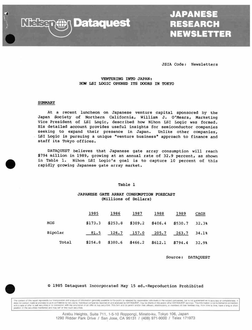
Dataquest JAPANESE RESEARCH NEWSLETTER
JSIA Code: Newsletters
VENTURING INTO JAPAN: HOW LSI LOGIC OPENED ITS DOORS IN TOKYO
SUMMARY
At a recent luncheon on Japanese venture capital sponsored by the Japan Society of Northern California, William J. O'Meara, Marketing Vice President of LSI Logic, described how Nihon LSI Logic was formed. His detailed account provides useful insights for semiconductor companies seeking to expand their presence in Japan. Unlike other companies, LSI Logic is pursuing a unique "venture business" approach to finance and staff its Tokyo offices.
DATAQUEST believes that Japanese gate array consumption will reach $794 million in 1989, growing at an annual rate of 32.9 percent, as shown in Table 1. Nihon LSI Logic's goal is to capture 10 percent of this rapidly growing Japanese gate array market.
Table 1
JAPANESE GATE ARRAY CONSUMPTION FORECAST (Millions of Dollars)
1985 1986 1987 1988 1989 CAGR
MOS
Bipolar
Total
$173.3
81.5
$254.8
$253.8
126.7
$380.6
$309.2
157.0
$466.2
$406.4
205.7
$612.1
$530.7
263.7
$794.4
32.3%
34.1%
32.9%
Source: DATAQUEST
1985 Dataquest Incorporated May 15 ed.-Reproduction Prohibited
The content of this report represents our interpretaion and analysis of information generalIy avaiIable to the public or reIeased by responsible individuals in the subject companies, but is not guaranteed as to accuracy or completeness. It does not contain materiaI provided to us in confidence by our clients Individual companies reported on and anaIyzed by DATAQUEST, may be cIients of ttiis and/or other DATAOUEST services This information is not furnished in connection with a sale or offer to seII securities or in connection with the solicitation of an offer to buy securities This firm and its parent and/or their officers, stockholders, or members of their families may, from time to time, have a long or short position in the securities mentioned and may sell or buy such securities
Azabu Heights, Suite 711, 1-5-10 Roppongi, IVIInato-ku, Tokyo 106, Japan 1290 RIdder Park Drive / San Jose, CA 95131 / (408) 971-9000 / Telex 171973

TAPPING INTO JAPAN'S VENTURE CAPITAL MARKET
Several years ago, Wilfred J. Corrigan, Chairman and Founder of LSI Logic/ concluded that to dominate the worldwide ASIC market, a successful venture in Japan was imperative in order to tap into lower lending rates and to be accepted by Japanese customers. But he wanted to avoid the traditional methods used by U.S. companies—joint ventures, wholly owned subsidiaries, and Japanese trading companies—which are often plagued with communications problems and culturally based management differences. Instead, LSI Logic decided to form a totally Japanese-run and Japanese-financed company to establish its credibility in Japan. Mr. Corrigan observed that the Japanese save a large percentage of their income, which is held by large pension, insurance, and banks that have few investment avenues except the stock market or treasury notes. (See our newsletter of May 29, 1984, "Japan's Second Venture Capital Boom".) Moreover, given Japan's immature venture capital market and few start-up companies, he reasoned that a large pool of funds could be tapped with the right management approach. Thus, he decided to form a new company—Nihon LSI Logic—which would have the following features:
U.S. ownership (70 percent) and minority stock share (30 percent)
All-Japanese management
Self financing
Design centers and a manufacturing plant in Japan
Stock sales within two to three years of founding
Licensing of LSI Logic technology
LSI Logic would act as an investor in the Japanese company, not as a multinational conglomerate issuing orders to a subsidiary. All operating decisions would be made in Japan. The new company would license LSI Logic's technology, and both companies would eventually exchange technology.
In late 1983, Mick Bohn, co-founder and Vice President of Finance at LSI Logic, visited Japan four times to present the plan to Japanese pension funds, banks, and insurance companies. Initially, the Japanese were wary, but gradually warmed to the idea due to growing interest in the ASIC market and venture businesses. However, to succeed in Japan, LSI Logic learned that it had to reverse its start-up formula. In Silicon Valley, entrepreneurs put together a strong management team, then seek venture capital financing. In Japan, top executives cannot be lured from lifetime jobs unless financing is solid. Thus, LSI Logic pursued financing first. It made a 35mm slide presentation of its plan to investors in Japanese, using simultaneous translators to permit free discussion. Meanwhile, it hired a large law firm, Nagashima & Ohno, to make Japanese investment advisors and government officials comfortable with LSI Logic's concept, and to ensure that LSI Logic met all of the Ministry of Finance's requirements.
- 2

The plan worked. In late 1983, Nomura Securities agreed to act as agent to sell minority shares in Nihon LSI Logic. In April 1984, 30 percent of the stock was sold to 28 private and large institutional investors, raising ¥4.5 billion ($20 million). Nihon LSI Logic was valued at $60 million—six times the original valuation of LSI Logic. (When LSI Logic was formed in 1981, venture capitalists paid $6 million for 60 percent ownership.) Eventually, Nihon LSI Logic plans to sell up to 50 percent of its stock to investors.
AMAKDDARI AMERICAN-STYLE
With its financing secured, Wilf Corrigan pulled off a major coup by hiring Keisuke Yawata of NEC America to head up Nihon LSI Logic. A spokesman for Japanese industry during his years in Silicon Valley, Mr. Yawata was slotted for a top management position in NEC upon his return to Japan. Over a period of a year, Mr. Corrigan met with Mr. Yawata regularly to discuss the new company. Both men even approached NEC's top management, but were initially refused. Thus, Mr. Yawata's move is an American version of what Japanese call "amakudari" ("descent from heaven", usually from a top ministry post to a private company), since the ability to attract top level managers reflects favorably on the recipient company.
NIHON LSI LOGIC'S PLANS
Under Mr. Yawata's leadership, Nihon LSI Logic has hired 20 Japanese in Tokyo, and plans to have 200 employees by 1986. All employees will be promoted on the basis of merit, not seniority, and will receive stock options. The company is opening its second design center in Japan and reviewing final sites for a $100 million manufacturing plant to be totally Japanese-financed. Initially, the plant will offer 1.5-micron CMOS technology, then sub-micron designs. Nihon LSI Logic's goal is to reach $100 million in sales by 1992, or 10 percent of the Japanese ASIC market.
LSI Logic is following the advice of Kenichi Ohmae, president of McKinsey & Company, who advocates in his book. Triad Power, that to compete internationally companies must establish a presence in Japan, Europe, and the United States. In October 1984, LSI Logic opened a $40 million plant in Fremont, California. In early 1985, it raised £20 million in London to build a plant in West Germany by selling 20 percent stock share. Nihon LSI Logic is part of this global strategy.
- 3 -

ENTERING THE JAPANESE MARKET
DATAQUEST believes that the only way to compete internationally with Japanese semiconductor companies is to establish a major presence in Japan. Companies such as Fairchild, Motorola, and Texas Instruments have successfully penetrated the bipolar market because of their local manufacturing capabilities. Recently, AMI, Nihon LSI Logic, and Thomson CSF have opened local design centers in Japan to enter the highly competitive ASIC market.
To finance and staff these operations, we believe that several routes are available to non-Japanese companies:
• Local financing:
— Japan Development Bank (JDB) loans—7.3 percent for research centers and plant facilities in any of the 15 Technopolis zones (such as Materials Research Corporation's Gita plant)
— Regional bank financing—Secured with the assistance of local prefecture industry and government leaders
Venture capital financing (Nihon LSI Logic)
— Local government tax incentives and special land writeoffs (Fairchild's Nagasaki plant, Monsanto's Utsunomiya plant)
-- Joint ventures with cash-rich conglomerates seeking new markets (AMI and Asahi Chemical)
• Staffing:
— Hire internationally minded Japanese executives with overseas experience (Nihon LSI Logic's Mr. Yawata, Motorola's Dr. Iriye, DATAQUEST's Mr. Morishita)
" Hire mid-level managers and professionals (IBM, DATAQUEST)
^ Establish joint technology development with a Japanese company (Thomson CSF and Oki)
Sheridan Tatsuno
- 4

Dataquest JAPANESE RESEARCH NEWSLETTER
JSIA Code: Newsletters
DATAQUEST'S JAPANESE CONFERENCE DEBUT— FAR EAST INDUSTRY: ACHIEVEMENTS AND CHALLENGES
SUMMARY
DATAQUEST's Japanese Semiconductor Industry Service (JSIS) held its first annual conference April 14-16 at the Hakone Prince Hotel, Hakone, Japan (south of Tokyo) . The conference was completely sold out. The 210 attendees heard 21 industry leaders, government officials, and DATAQUEST analysts speak at this first-ever, full-length DATAQUEST Japanese conference. Speakers and attendees represented U.S., European, Japanese, Korean, and Taiwanese companies and government agencies. It is particularly noteworthy that more than half of the attendees were Japanese, and about the same percentage were top-level executives. Keynote speakers were Dr. Atsuyoshi Ouchi, Vice Chairman of NEC Corporation, and Mr. W. J. Sanders III, Chairman, President, and CEO of Advanced Micro Devices, Inc.
The conference theme, "Far East Industry: Achievements and Challenges," was particularly timely because of the great achievements made by the Japanese semiconductor industry in the last five years, the emergence of Taiwan and Korea as fast-growing participants in the semiconductor industry, and the highly publicized challenge being posed to U.S. and European suppliers in their attempts to penetrate Japanese industry.
This newsletter will cover the major topics addressed at the conference in the areas of market trends and strategies, trade and technology issues, equipment and materials, and product trends. Conference notebooks were distributed to all conference attendees and will be mailed to subscribers who did not attend the conference. Readers who wish to read specific speeches should contact their companies' JSIS notebook holder or conference attendee.
1985 Dataquest Incorporated May 8 ed.-Reproduction Prohibited
The content of this report represents our interpretaion and analysis of information generally available to the public or released by responsible individuals in the subject companies, but is not guaranteed as to accuracy or compIeteness. It does not contain material provided to us in confiIJence by our clients Individual companies reported on and analyzed by DATAQUEST, may be clients of this and/or other DATAQUEST services This information is not furnished in connection with a sale or offer to sell securities or in connection with the solicitation of an offer to buy securities. This firm and its parent and/or their officers, stocltholders, or members of their families may, from time to time, have a long or short position in the securities mentioned and may seII or buy such securities
Azabu Heights, Suite 711, 1-5-10 Roppongi, Iy/llnato-ku, Tokyo 106, Japan 1290 Ridder Park Drive / San Jose, CA 95131 / (408) 971-9000 / Telex 171973

MARKET TRENDS AND STRATEGIES
Overview
DATAQUEST's Fred Zieber, Senior Vice President and Semiconductor Division Manager, kicked off the conference with an updated world semiconductor outlook. Predicting that the worldwide semiconductor market will grow only 2 percent in 1985, he blamed the disastrous first quarter of 1985 on a confluence of tremendous change in expectations, overbookings, a weak PC market, and very high prices in early- and mid-1984, which fell like a rock. He cited a growing U.S. economy and growth in real semiconductor usage as reasons for continued long-term growth of the industry. Mr. Zieber also pointed out the increasing ratio of materials cost to manufacturing, and projected a steadily decreasing trend for return on capital invested.
Sheridan Tatsuno, JSIS Research Analyst and author of an upcoming book entitled "Technology: Japan's HiTech Strategy for the 21st Century," noted a high correlation between the growth of Japanese-based companies' share of the world IC market, the Japanese share of the U.S. IC market, and the steadily increasing Japanese companies' share of papers presented at the International Solid State Circuits Conference. This correlation suggests that Japan is moving ahead quickly in both sales and technological expertise. He pointed to the dramatic increase in joint ventures and licensing between Japanese and Other firms as signaling a change from the "we vs. them" philosophy to a new philosophy of sharing and working together. Mr. Tatsuno presented DATAQUEST's forecast of 7 percent growth for the Japanese market in 1985, with a caution that this figure is at the upper end of our current range of 0 to 7 percent.
Japanese Viewpoint
Tomihiro Matsumura, Senior Vice President of NEC, spoke on "Japanese Semiconductor Industry—The Coming New Age." (Mr. Matsumura received a special award from Japan's Ministry of Science and Technology on the day he spoke at the DATAQUEST Conference, for his work in developing NEC's V-Series of originally developed microprocessors.
He noted that only two Japanese semiconductor companies were in the top ten worldwide in 1975, while in 1984, five were in the top ten. He believes that this is due to:
• Creating new markets (i.e., not just waiting for the economy to turn up)
• Emphasizing mass production rather than R&D
• Having available a much larger pool of engineering graduates to draw from than either the United States or Europe
- 2 -

Regarding export sales, Mr. Matsumura suggested that to ease trade friction, 50 percent of overseas sales should be produced in the country in which they will be sold.
Tsuyoshi Kawanishi, Director and Group Executive of Toshiba, spoke on the topic "Concentrated or Well-Balanced Products Strategy?" He believes that in general, U.S. semiconductor companies tend to concentrate on specific products, while Japanese companies tend to have more balanced product lines including heavy emphasis on discrete devices. While the concentrated strategy offers capital investment concentration, clear strategy, a strong corporate image in the areas of concentration, and phases of extremely high growth, it also leads to decreased stability during downturns and an inability to provide customers with a full line of products. On the other hand, the well-balanced strategy offers technology growth due to interrelationships of products, stability, and ability to service all the customers' needs. Drawbacks include a weak corporate image, unclear strategy, and inability to concentrate capital investment.
Korea and Taiwan
Irving T. Ho, President of Taiwan's Institute of Information Industry and the holder of 36 patents in computer hardware and subsystems, spoke on "The Recent Development of the Information Industry in Taiwan." In 1979, Taiwan instituted a strategic policy of developing a domestic information industry. The results of this policy are dramatic. In 1983, for the first time, Taiwan's electrical and electronic exports exceeded textile exports. Information product exports, especially computers, have experienced the highest growth of any electronics products. Dr. Ho provided information on the major electronics producers and exporters in Taiwan, and discussed major products and companies. He revealed the heavy investment plans of IC producers in Taiwan over the next three to five years. All IC manufacturers in Taiwan cooperate extensively with ERSO, the semi-governmental IC technology company. ERSO now has 2-micron Si-gate CMOS technology with single poly and double metal.
P. June Min, Senior Managing Director of Goldstar Semiconductor, Ltd., spoke on "The Emerging Korean Semiconductor Industry." Dr. Min presented many tables detailing semiconductor production and consumption in Korea, for which he sees very high growth in the next several years. The Korean electronics industry began with Korean companies manufacturing for Others on an OEM basis. Today, Korean name brand goods are sold worldwide. As in Japan, Korean semiconductor companies are parts of large, vertically integrated organizations. Also similarly to the Japanese, Korean companies are obtaining much of their design technology through licensing agreements with U.S. and European firms, although their processing technology is domestically developed. Dr. Min expects Korean semiconductor sales to triple by 1988.
- 3 -

A U.S. Look at Japan
Eugene J. Flath, Vice President and Assistant General Manager of Intel International, spoke on "A Fresh Look at Japan and Asia," a topic for which he is well qualified, having recently moved to Japan and become responsible for expanding Intel's presence in Japan and the Pacific Basin. Mr. Flath outlined the history of the U.S. semiconductor industry, which began with vertically integrated companies and now consists of many small- to mid-size companies specializing in semiconductors. This current state contrasts with the Japanese industry, which is dominated by vertically integrated manufacturers. He believes that due to the continually escalating cost of materials, most new capacity expansion will be in the Pacific Basin. He also believes that in order to support the Japanese market in a major way, foreign companies must build manufacturing facilities in Japan. This represents a radical change of view on Intel's part.
TRADE AND TECHNOLOGY
The areas of international trade and cooperation and government policy were very timely, since the conference was held during the height of tension in the trade negotiations between the United States and Japan.
Keynote Speakers
The conference keynote speakers, Atsuyoshi Ouchi of NEC and W. J. Sanders III of AMD, both spoke on these issues at dinner.
Dr. Ouchi struck a conciliatory tone regarding international trade relations. He believes that if the captive portion of the U.S. semiconductor market is accounted for, then Japanese companies actually have a smaller portion of the U.S. semiconductor market than the U.S. companies have of the Japanese semiconductor market. He also reminded Mr. Sanders that NEC is a major purchaser of AMD's ICs. Dr. Ouchi compared the completely open semiconductor market, which he thinks should exist, with contract bridge. He said that in a properly operating market, as in contract bridge, partners give each other signals that can be seen and understood by all partners, and all players follow the same rules. The perception now is that too much of the game is being played behind closed doors.
Mr. Sanders spoke pointedly on the U.S.-Japan trade imbalance and the difficult barriers U.S. companies face in the Japanese marketplace. While supporting the need for free international trade as vital to the free world's economic security, he termed the current imbalance "intolerable," and called for the United States to act unilaterally to provide incentive—in the form of U.S. trade barriers—to promote more openness in Japanese markets. Mr. Sanders supported his statement that barriers do exist in the Japanese semiconductor market by demonstrating that U.S. firms outperform their Japanese counterparts in the neutral markets of Europe and Rest of World. He called for "affirmative action" on the part of Japanese companies and consumers to buy more U.S. goods.
- 4 -

Government View
Clyde Prestowitz, Counselor on Japan to the U.S. Secretary of Commerce, spoke on "Government Involvement: Help or Hindrance." He noted that the U.S. government has both helped and hindered the U.S. semiconductor industry. While aiding the industry through military procurement, the Department of Defense (DoD) also hinders its ability to exploit overseas markets because the DoD makes it difficult to obtain the necessary export licenses. On the other hand, the Japanese government's efforts have been more focused and more continuous in aiding the Japanese semiconductor industry. He believes that in the matter of trade, there has been a lot of talk but little communication. He also cited several examples of instances in which, because of the bureaucratic Japanese system, U.S. companies were discriminated against, even though discrimination may not have been intended. Mr. Prestowitz noted that the Japanese still view themselves as a very small, developing country. He has been told, during the course of his trade negotiations, that "little baby companies" such as NEC and Hitachi cannot compete with "great sumo wrestler companies" like IBM and AT&T on a global basis.
Presenting the Japanese government's perspective was Shoichi Ito, a technical official from the Ministry of International Trade and Industry (MITI) . Mr. Ito stood in for Hiroshi Shima, who was called at the last minute to testify in the Diet on the proposed Japanese chip protection act. Mr. Ito's topic was, "Status Quo and Tomorrow, Japanese Semiconductor Industry." He stated MITI's position that Japan and the United States "should strive for even freer semiconductor trade, and work to avoid regulative actions while eliminating any existing trade barriers." He believes that much progress has been made in Japan with U.S. electronics trade talks, and that they have resulted in concrete benefits. According to MITI's statistics, U.S. companies' individual growth rates in Japan in the last two years have been between 40 and 100 percent. Mr. Ito concluded by calling for further deepening of mutual understanding between Japan and the United States through such organizations as the U.S.-Japan Work Group on High-Technology Industries.
Industry View
William G. Howard, Jr., Corporate Director of R&D for Motorola, Inc., spoke on "Technology Futures." Dr. Howard described a report on international competitiveness published by the British government about the United States in 1855. The report described the mass production technology developed in the United States, and cited application of the principles of diligent management, creative ideas, and hard work as the factors that made U.S. industry far more efficient and internationally competitive than British industry. He believes that there are parallels between this British history and the United States today. To support his belief that the focus of the electronics industry is shifting from the Atlantic to the Pacific Basin, he cited three facts:
• Since 1979, international market share has fallen for all but one U.S. electronics company.
- 5 -

• The United States had an overall electronics trade deficit of $6.8 billion in 1984.
• The number of U.S.-origin patents has been decreasing since its 1971 peak, while the number of Japanese-origin patents has steadily climbed.
EQUIPMENT AND MATERIALS
Three industry leaders who are directors of their respective companies, Jon D. Tompkins of Varian Associates, Kihachi Tamura of Shin-Etsu Handotai Co., Ltd. (SEH), and Shoichiro Yoshida of Nippon Kogaku K.K. (Nikon), spoke on equipment and materials issues.
Mr. Tompkins spoke on "Challenges and Opportunities Facing U.S. Equipment Suppliers in Japan." He believes that the Japanese market can be very good for U.S. suppliers because it is the largest world market for capital equipment and offers a ready market for leading-edge manufacturing tools. He perceives that Japanese companies are becoming more willing to share technology with U.S. equipment companies in order to ensure the availability of manufacturing equipment for DRAMs of 1Mb and beyond. He stressed the importance of maintaining U.S. manufacturing and service organizations in Japan for customer support. He expressed his belief that Japanese companies will not adopt the SECS II communications protocol standard adopted by SEMI, and warned that if this happens, U.S. companies will find it much more difficult to compete in the Japanese marketplace for automated manufacturing.
Mr. Tamura focused his presentation on his estimates of the world's silicon markets. He believes that Japanese silicon consumption has been somewhat overestimated in the past while U.S. silicon consumption has been understated, primarily due to captive U.S. consumption, which has not been included. He believes that total U.S. silicon consumption is higher than Japanese silicon consumption, and that Japanese 6-inch wafer consumption is higher proportionally than U.S. 6-inch wafer consumption. He expects the percentage to be twice as high as the U.S. percentage in 1985, as more 6-inch lines come onstream in Japan. He noted that high oxygen content in wafers is very popular in the United States. SEH will begin experimental production of 8-inch wafers this year, but he would not reveal plans for 10- and 12-inch wafers.
Mr. Yoshida spoke on "Lithography Technology; Today and Tomorrow." His speech focused on lithography trends for increasing semiconductor device integration. Citing the fact that chip density tends to increase by four times every three years, he stated his belief that stepper technology can be used through the 4Mb DRAM. For 16Mb DRAMs and beyond, he believes that the lithographic method must be x-ray or e-beam. Mr. Yoshida has been named Secretary-General of the newly formed Semiconductor Equipment Association of Japan. He expects 1985 capital expenditures to be down from 1984.
- 6 -

PRODUCT TRENDS
Sutezo Hata, Executive Managing Director of Hitachi, and Lane Mason, Senior Industry Analyst in DATAQUEST's Semiconductor Industry Service, both spoke on MOS memory.
Mr. Hata believes that MOS memory is "the propulsion power of the IC industry." He cited the high volume of the market, high historical growth, and the fact that MOS memory technology is a catalyst for the development of other IC technologies. Hitachi is intensively promoting CMOS technology, due to its low power consumption. Mr. Hata outlined the history of MOS memory development and the diverse types of MOS memory that are now available, such as OTP PRCMs and pseudo SRAMs. He pointed to the pervasiveness of MOS memory in the form of built-in memories in a system and dedicated memory chips. He also described how increasing integration has led to decreasing line widths, and predicted that 16Mb DRAMS will require line widths of 0.5 micron.
Mr. Mason spoke on "MOS Memory Strategies: Face to Face With the New Market Realities." He discussed the rapidly changing complexion of the market, with prices and profits rising in 1983 and 1984, only to come crashing down in the second half of 1984. He believes that 1985 and 1986 will be awash in red ink for MOS memory suppliers that have ill-defined strategic plans or poor manufacturing efficiency. He stated that in the MOS memory market, a cost-driven strategy will beat out a technology-driven strategy. He recommended that to succeed in the market, companies should commit themselves to the long haul and possibly find emerging niche markets in order to differentiate their products, although the mainstream market of standard, commodity products will continue to be the primary revenue growth vehicle for the foreseeable future.
Richard L. Sanquini, Vice President and General Manager, Microprocessor Group, of National Semiconductor Corporation, spoke on "Fundamental Forces Driving the 32-Bit MPU Market." Mr. Sanquini believes that the 32-bit market will be much larger than many believe. The 32-bit MPUs offer more performance per price per unit area than 8- or 16-bit machines. They allow more tasks to be performed in parallel, thus reducing nonproductive periods. Today's applications for 32-bit MPUs include desktop and engineering workstations, robotics, file servers, satellite processors, communication networks, and data links. In the future, he sees artificial intelligence becoming an important 32-bit application. He believes that by 1990, 32-bit "computing clusters"—each consisting of 32-bit CPU, MMU, FPU, and ICU—will account for a $900 million market, and that 32-bit MPUs will be an integral part of most systems, with 8- and 16-bit MPUs taking secondary roles.
D. A. DiLeo, I.C. Product Marketing Manager for AT&T Technology Systems, focused on custom MOS ICs in his presentation. He noted the increasing pervasiveness of semiconductors in AT&T's telecommunications equipment, which is forecast to grow by a factor of three from 1979 to 1989. He gave an example of a system in which cost was reduced by four times and parts were reduced by ten times, by replacing eight boards with one board containing ten custom chips. The average AT&T custom IC design
- 7 -

rule is now 1.5 microns, and by 1987 this will have decreased to 1.0 micron. As design rule has decreased, so has gate delay time. Average gate delay time is now 0.7 ns. AT&T's goal is to integrate CODECS, protocol controllers, signal processing, and ISDN basic access into one custom integrated system on a chip.
PANEL DISCUSSION
The conference ended with a stimulating panel discussion. Questions solicited from the attendees during the course of the conference were presented to a panel consisting of David Laws of AMD, Mr. Flath, Rick Younts of Motorola, Dr. Min, Mr. Hata, and Mr. Kawanishi. Hard-hitting questions were handled very well by the panel members.
1986 JSIS CONFERENCE
The 1986 JSIS conference will be held April 13-15 at a location in Japan to be announced soon. We believe that the focus of this conference will be on the emerging applications for VLSI, such as telecommunications, artificial intelligence computers, new consumer media, and manufacturing automation.
Patricia S. Cox
- 8 -

Dataquest JAPANESE RESEARCH NEWSLETTER
JSIA Code: Newsletters
U.S.-JAPAN TRADE: EAST LEADS WEST
INTRODUCTION
U.S.-Japan trade is an issue of great concern in both industrial and government circles. Over the last ten years, the total U.S. trade deficit with Japan has increased twentyfold. Particularly hard-hit have been the high-tech industries. We sense a severe agitation on the part of both U.S. industry and government officials.
U.S. trade with Japan hit record levels in 1984, with total trade increasing 28 percent to $80,710 million. The overall U.S. trade deficit with Japan grew 74 percent, from negative $19,289 million to negative $33,560 million. Table 1 shows U.S.-Japan trade statistics for all merchandise, beginning in 1975. As this table shows, while U.S. exports of all merchandise to Japan grew at a compound annual growth rate (CAGR) Of 11 percent from 1975 to 1984, U.S. imports from Japan grew at a CAGR of 20 percent during the same period.
Trade in electronic equipment and semiconductors also showed dramatic growth in 1984. In 1984, electronic equipment imports from Japan represented 32 percent of all U.S. imports from Japan; in 1975, it had been only 17 percent.
U.S.-JAPAN TRADE IN ELECTRONIC EQUIPMENT
As shown in Table 2, U.S. imports of electronic equipment from Japan experienced a CAGR of 35 percent from 1981 to 1984. Growth has been particularly dramatic in computers, which increased in sales by an order of magnitude over the four-year period. Consumer electronic product imports grew 52 percent in 1984 alone.
© 1985 Dataquest Incorporated April 4 ed.-Reproduction Prohibited
The content of this report represents our interpretaion and analysis of information generally avaiIable to the public or reIeased by responsible individuals in the subject companies, but is not guaranteed as to accuracy or compIeteness It does not contain material provided to us in confidence by our clients Individual companies reported on and analyzed by DATAQUEST, may be clients of this andlor other DATAQUEST services This information is not furnished in connection with a sale or offer to sell securities or in connection with the solicitation of an offer to buy securities This firm and its parent and/or their officers, stockholders, or members of their families may, from time to time, have a long or short position in the securities mentioned and may sell or buy such securities.
Azabu Heights, Suite 711, 1-5-10 Roppongi, Minato-ku, Tokyo 106, Japan 1290 Ridder Park Drive / San Jose, CA 95131 / (408) 971-9000 / Telex 171973

Table 3 shows the U.S. trade deficit with Japan in electronic equipment. From 1975 to 1984, U.S. imports from Japan increased at a CAGR of 28 percent, 4 percent higher than U.S. exports to Japan. The huge amount of electronic equipment imported from Japan to the United States in 1984—$18,122 million—resulted in a U.S. deficit of $15,448 million, 72 percent higher than in 1983. This large deficit in electronic equipment is almost half of the entire U.S. trade deficit with Japan.
Figure 1 graphically depicts U.S.-Japan trade in electronic equipment from 1975 to 1984.
U.S.-JAPAN TRADE IN SEMICONDUCTORS
U.S.-Japan semiconductor trade, as measured by the U.S. Department of Commerce, grew to a total of $1,876 million in 1984. Tables 4 and 5 show U.S. semiconductor exports to Japan, U.S. semiconductor imports from Japan, and the U.S. semiconductor trade balance with Japan. These numbers are stated at import and export valuation.
DATAQUEST's estimates of total semiconductor sales (stated at actual market value and inclusive of locally manufactured product) are shown in Tables 6 and 7. Table 6 presents DATAQUEST's estimates of U.S. sales of semiconductors in Japan and Japanese sales of semiconductors in the United States. Table 7 presents DATAQUEST's estimate of the U.S.-Japan account balance in semiconductors. Figure 2 shows the U.S.-Japan semiconductor balance graphically.
From 1982 to 1984, U.S. semiconductor sales in Japan grew at a CAGR of 49 percent, from $446 million to $992 million. Strong areas for the United States include bipolar digital ICs and industrial linear ICs. Over the same period, Japanese semiconductor sales in the United States grew at a CAGR of 63 percent, from $787 million in 1982 to $2,100 million in 1984. By far the strongest products for the Japanese are MOS memory and logic devices. Sales of MOS memory by Japanese companies in the United States reached an estimated $1,409 million in 1984. DATAQUEST estimates the U.S. deficit with Japan in this area to be negative $1,252 million, resulting in a U.S. total semiconductor deficit of $1,108 with Japan in 1984. This U.S. deficit grew at a CAGR of 80 percent from 1982 to 1984.
The U.S. MOS market is clearly of paramount importance to Japanese suppliers. In 1984, 32 percent of all Japanese MOS sales were in the United States, as shown in Figure 3. In contrast, only 6 percent of U.S. MOS sales were in Japan, as shown in Figure 4.
The Japanese share of the U.S. semiconductor market, which stood at 12.0 percent in 1982, reached 17.4 percent in 1984, as shown in Table 8. Of this, Japanese companies held 44.0 percent of the U.S. MOS memory market, and 10.7 percent of the U.S. MOS logic market. From 1982 to
- 2 -

1984, U.S. companies gained only nine-tenths of a percentage point in their share of the Japanese semiconductor market, which was 11.9 percent in 1984. The largest U.S. share is in bipolar digital ICs, of which U.S. companies hold 34.2 percent of the market.
CONCLUSION
DATAQUEST believes that the U.S. semiconductor market is clearly the most strategically important marketplace for the Japanese semiconductor industry, accounting for 19 percent of all Japanese company worldwide sales. We expect Japanese companies to maintain U.S. market share during 1985 in a falling U.S. market, and poise themselves to increase market share in 1986 when the U.S. market picks up again.
At the same time, we believe that U.S. companies will continue to establish more sales, design, and perhaps manufacturing facilities in Japan, in order to form the local relationships necessary to successfully sell intu} the Japanese market.
The U.S. government is taking an increasingly aggressive stance toward perceived trade barriers in the Japanese market. We believe that in 1985, considerably more pressure than heretofore will be put on the Japanese government to reduce trade barriers and redress the U.S.-Japan trade imbalance, particularly in automobiles and electronics.
Patricia S. Cox
- 3 -

Table 1
ESTIMATED TRADE BALANCE FOR ALL MERCHANDISE
UNITED STATES VS. JAPAN
(Millions of Dollars)
Veor
1975
1980
1981
1982
1983
1984*
U.S.
Exports
to Japan
$9,567
$20,806
$21,796
$20,966
$21,894
$23,575
U.S.
Imports
f rom Jopan
$11,257
$31,217
$37,598 $37,744
$41,183
$57,135
U.S.
Trade Balance
($1,690)
($10,411)
($15,802)
($16,778)
($19,289)
($33,560)
CAGR 1975-1984 >1% 207: 39%
•Preliminary
Table 2
ESTIMATED U.S. IMPORTS OF ELECTRONIC EQUIPMENT FROM JAPAN
(Millions of Dollars)
1981 1982 1983 1984*
Communications $961 $1,109 $1,391 $2,077 Components
(including semiconductors) $962 $1,233 $1,741 $3,450
Computers $387 $822 $1,762 $3,200
Consumer electronics $3,646 $3,410 $3,985 $6,040
Instrumentation $592 $566 $701 $985
Office Products $1,338 $1,379 $1,602 $2,370
Total $7,886 $8,519 $11,182 $18,122
CAGR
1981-84
29%
53%
102%
18%
18%
21%
32%
•Preliminary
Source: U.S. Oept. of Commerce DATAOUEST
- 4 -

Table 3
0) I.
"5 o
n c ,o
IB
ESTIMATED ELECTRONIC EQUIPMENT TRADE BALANCE
UNITED STATES AND JAPAN
(Millions of Dollars)
Yeor
1975
1980
1981
1982
1983
1984*
CA6R
•Pre!
1975-1984
iminory
U.S. Exports
to Jopan
$397
$1,058
$1,857
$1,941 $2,187
$2,674
24S5
FigurI
U.S. Imports
from Jopan
$1,903
$5,012
$7,886
$8,519
$11,182
$18,122
28%
Source: U S.
U.S.
Trade Balance
($1,506)
($3,954)
($6,029)
($6,578)
($8,995)
($15,448)
30%
Dept. of Commerce
DATAQUEST
B 1
U.S.-JAPAN TRADE IN ELECTRONICS
1975
UTT] U.S.-Japan
1981 1982 1983 1984*
r 3 3 Japan-U .S . ZPZ^ U.S. Balance
S o u r c e : DATAQUEST
- 5 -

Table 4
U . S . SEMICONDUCTOR TRADE WITH JAPAN*
( M i l l i o n s o f D o l l a r s )
Exports to Japan Imports from Japan Export Import
CAGR CAGR
1982 1983 1984 1982 1983 1984 19S2-84 1962-84
Tota l Semiconductor $132 $183 $250 $495 $729 $1 ,626 38% 81%
Tota l IC $120 $170 $234 $435 $666 $1 ,521 40% 87%
Bipo lo r D i g i t a l $26 $34 $48 $72 $74 $133 36% 36%
MOS liIlemory $36 $34 $43 $295 $464 $1 , 009 9% 85%
lyOS Logic $40 $53 $58 $45 $100 $309 20% 162%
L inear $ 1 8 $49 $85 $23 $28 $69 117% 74%
Tota l D i s c r e t e $12 $13 $ 1 6 $60 $63 $105 15% 32%
• S t a t e d at import and export va lues
Table 5
U . S . SEMICONDUCTOR TRADE BALANCE WITH JAPAN*
( M i l l i o n s o f D o l l a r s )
CAGR
1982 1983 1984 1982-84
Tota l Semiconductor ($363 ) ( $546) ( $ 1 , 3 7 6 ) 95%
Tota l IC ($315 ) ($496 ) ( $ 1 , 2 8 7 ) 102%
Bipolar Digital ($46) ($40) ($85) 36%
MOS Memory ($259) ($430) ($966) 93%
MOS Logic ($5) ($47) ($251) 609%
Linear ($5) $21 $16
Total Discrete ($48) ($50) ($89) 36%
•Stated at import and export values
Source: U.S. Dept. of Commerce
DATAQUEST
- 6 -

Table 6
ESTIMATED U.S. SALES OF SEMICONDUCTORS IN JAPAN VS. ESTIMATED JAPANESE SALES OF SEMICONDUCTORS IN THE UNITED STATES*
(Millions of Dollars)
U.S. Sales in Japan
Japanese Sales
in U.S. U.S.—Japan Japan-.U.S.
1982 1983 1984 1982 1983 1984
Total Semiconductor $446 $600 $992 $787 $1,149 $2,100
Total IC $389 $539 $917 $711 $1,071 $1,987
Bipolar Digital $154 $190 $326 $90 $93 $144
MOS Memory $47 $62 $157 $535 $818 $1,409
MOS Logic $75 $135 $212 $57 $125 $359
Linear $113 $152 $222 $29 $35 $75
CAGR
1982-84
49%
54%
45% 83X 68% 40%
CAGR
1982-84
6;ss
67%
26% 62% 151%
61%
Total Discrete $57 $61 $75 $76 $78 $113 15% 22%
•Estimated sales by U.S. and Japanese companies
Table 7
ESTIMATED U.S. SEMICONDUCTOR ACCOUNT BALANCE WITH JAPAN*
(Millions of Dollars)
1982 1983
Totol Semiconductor ($341) ($549) ($1,108)
CAGR
1984 1982-84
Total IC
Bipolar Digi tal
MOS Memory
MOS Logic
Linear
Total Discrete
($322) ($532) ($1,070)
$64 $97 $182
($488) ($756) ($1,252)
$18 $10 ($147)
$84 $117 $147
($19) ($17) ($38)
80%
82%
69%
60%
32%
41%
•Estimated sales by U.S. and Japanese companies
Source: DATAQUEST
- 7 -

Figure 2
U.S.-JAPAN TRADE IN SEMICONDUCTORS
e JO
1
2.2 2.0 1.8 1.6 1.4. ^Jt 1.0 0.8 0.6 0.4-0.2 0.0
-0.2 -0.4--0.6--0.8 -1.0 H -1.2
: ^
1980
17^ U.S.—Japan
i l '^^^ ^^
^
^ ^ P7^ J
1
19B1 1982
J^S Jopon-U.S.
i i I
1983 1984
^ ^ U.S. Balanca
Figure 3
JAPANESE MOS SALES IN THE UNITED STATES AND WORLDWIDE 1984
Japan-WW (68.2%)
Japan-U.S. (31.8%)
Source: DATAQUEST
- 8 -

Figure 4
U.S. MOS SALES IN JAPAN AND WORLDWIDE 1984
U.S.-Japan (5.9%)
U.S.-WW (94 .1%) Source: DATAQUEST
Table 8
ESTIMATED U.S. SHARE OF THE JAPANESE MARKET AND ESTIMATED JAPANESE SHARE OF THE U.S. MARKET
(Percent)
U.S. Shore of the Japanese Market
1982 1983 1984
Total Semiconductor 11.0% 10.8% 11.9%
Japanese Share of the U.S. Market
1982 1983 1984
12.0% 13.7% 17.4%
Total IC 13.6% 13.6% 14.9% 13.5% 15.3% 19.3%
Bipolar Digital 29.5% 28.9% 34.2% 6.7% 5.4% 6.0% MOS Memory 8.0% 6.4% 7.6% 35.7% 40.3% 44.0% MOS Logic 11.5% 13.9% 15.8% 3.6% 5.8% 10.7% Linear 10.3% 11.2% 12.2% 3.4% 3.2% 5.5%
Total Discrete 4.7% 3.8% 3.4% 5.9% 5.7% 6.5%
Source: DATAQUEST
- 9 -

JSIA Code: Newsletters
SEMICONDUCTOR CONSUMPTION IN JAPAN EXPLODES IN 1984
SUMMARY
If you weren't in Japan in 1984, you missed a great opportunity. Not since 1976, the year of the CB radio boom, has the Japanese semiconductor industry grown at such a pace. Fueled by the boom in personal computers, telecommunications, office automation, and factory automation products, the industry grew an estimated 51.8 percent, reaching $8.3 billion. This figure compares with a U.S. market of $12.1 billion.
JAPANESE SEMICONDUCTOR CONSUMPTION
Although it still ranks number two after the United States, the Japanese market has grown from 54.5 percent of the U.S. market in 1980 to 69.4 percent in 1984, as shown in Figure 1. In the hotly contested integrated circuit market it is even more dramatic. In 1980 it was 45 percent of the U.S. market; in 1984 it was 61 percent.
One should also note that in 1983, Japanese consumption of discretes surpassed that of the United States. We believe that this is due to the voracious appetite of VTRs for these devices. Table 1 shows our analysis of the semiconductor composition of a typical medium-range VTR. If one multiplies these devices by the total 1984 Japanese VTR production of 28 million units, it is easy to see why the Japanese discrete market has grown to surpass that of the United States.
Table 2 shows DATAQUEST's semiconductor consumption analysis. It shows that consumption of ICs grew 57.5 percent in 1984. Price firmness, which can be attributed to a shortage of supply of the dominant products such as 64K DRAMs, 8-bit MCUs, and TTL Schottky MSI devices, caused some of the high growth, but we believe that strong demand for office automation products was the principal culprit.
© 1985 Dataquest Incorporated March 29 ed.-Reproduction Prohibited
The content of this report represents our interpretaion and analysis of information generally avaiIable to the public or released by responsible individuals in the subject companies, but is not guaranteed as to accuracy or completeness It does not contain material provided to us in confidence by our clients Individual companies reported on and analyzed by DATAQUEST, may be clients of this and/or other DATAQUEST services This information is not furnished in connection with a sale or offer to sell securities or in connection with the solicitation of an offer to buy securities This firm and its parent and/or their officers, stockholders, or members of their families may, from time to time, have a long or short position in the securities mentioned and may sell or buy such securities
Azabu Heights, Suite 711, 1-5-10 Roppongi, Minato-ku, Tokyo 106, Japan 1290 Bidder Park Drive / San Jose, CA 95131 / (408) 971-9000 / Telex 171973

Audio equipment and the rapid growth of compact disk (CD) players caused additional pressure on the semiconductor suppliers. However, as the U.S. market began slowing at the end of 1984, so did the Japanese market. The U.S. book-to-bill ratio, as measured by the World Semiconductor Trade Statistics Program, plummeted from 1.53 in January to 0.58 in December. We believe that as the United States began an inventory correction that will last through first quarter 1985, there has been a concurrent softness in Japan's personal computer market, causing semiconductor consumption to flatten out. As a result, we believe that fourth quarter 1984 domestic shipments grew only 5.0 percent over the third quarter, as shown in Table 2. This flattening can also be attributed to an inventory of VTRs both in the United States and Japan.
MARKET SHARE EXPLOSION IN THE UNITED STATES
Japanese manufacturers have quietly been gaining market share in the United States over the last several years. In 1984 they made the largest gain of the last five years, with the Japanese share of the U.S. market growing 3.5 percentage points to reach 17.4 percent (see Figure 2). In integrated circuits, we believe that the Japanese share of the U.S. market in 1984 was 19.4 percent, an increase of 4 percentage points over 1983. Even though the Japanese domestic market was experiencing a semiconductor shortage similar to that in the United States, we believe that for six to eight months, the Japanese continued to support large U.S. users of 64K DRAMs, and in many cases enjoyed a $1.00 premium per device over the same product sold in Japan. Furthermore, we believe that Japan's 1984 share of the U.S. MOS memory market grew 3.7 percentage points, and that the Japanese can now claim 44 percent of the U.S. MOS memory market.
REVISED OUTLOOK FOR 1985
We now believe that 1985 will be somewhat slower than it appeared in our September outlook. We have adjusted our predictions due to the following factors:
f Economic activity is moderating and we believe that 1984's real GNP growth rate of 5.3 percent will slow to a projected growth of 4.5 percent (based on the Japanese government's recently released economic forecast of December 1984).
• The inventory of VTRs has risen for two quarters.
• There is a glut of PCs in both the United States and Asia.
• Capital expenditures of the Japanese and U.S. semiconductor manufacturers rose to $6.2 billion during 1984, which has precipitated an overcapacity for the current level of demand, especially for MOS memories.
- 2 -

We expect this overcapacity to result in pricing below the learning curve through 1985. Incidentally, MOS memory represented about 30 percent of the total U.S. market for semiconductors and 20 percent of the Japanese semiconductor marlcet.
Our forecasted growth rate for 1985 for total consumption is 7.0 percent, with discretes decreasing 2.6 percent and ICs growing 10.4 percent. The sectors of the Japanese electronics industry that we expect to be the most healthy will be telecommunications, new consumer media such as Videotex, high-resolution TV monitors, CAD/CAM, minifax for home use, and compact disc players. DATAQUEST believes that CDs will be the next high-volume consumer product. We estimate that 1.2 million units will be produced in 1985, up from 740,000 in 1984. From a quarterly pattern perspective, we believe that first quarter 1985 semiconductor consumption will be down relative to fourth quarter 1984 by 11 percent. Quarterly consumption changes are shown in Figure 3. Severe pricing pressures in memories and a general inventory adjustment are causing consumption to drop in value. New orders are not anticipated to increase until mid-second quarter. Because of the March fiscal year end date used by most Japanese companies, end users are currently adjusting their inventories as they prepare for the start of the new fiscal year.
Gene Norrett Patricia S. Cox
- 3 -

Figure 1
JAPANESE SEHICONDtTCTOR CONSUMPTION COMPARED TO U . S . SEMIC(»tDUCTOR CONSUMPTION
12-
11-
10-
9-
»-
7-
6-
5-
4-
3-
2-
1-
Q Japan % of U.S. Market
EH "c PVH Disc
^
' ii r 1 i 1 I j I
1980 Japan U.S.
1982 Japan U.S.
1984 Japan U.S.
Source: OATAOUEST
Table 1
ESTIMATED SEMICONDUCTOR CONSUMPTION OF JAPANESE VTRs
20 Optoelectronic devices
170 Diodes
120 Transistors
30 MSI ICs (linear and digital)
3 Microcontrollers
Source: DATAQUEST
- 4 -

Table 2
ESTIMATED JAPANESE SEMICONDUCTOR CONSUMPTION (Billions of Yen)
1983
Discrete IC*
Total
Percent Change from Previous Quarter
Ql
74.1 188.8
262.9
2.5%
Q2
91 .1 218.5
309.6
17.8%
Q3
103.7 248.6
352.5
13.9%
Q4
105.8 272.5
378.3
7.3%
Total Year
374.7 928.6
1.303.3
Percent Change from Previous Year
5.9% 29.4% 33.1% 47.5% 29.2%
1984
Discrete IC*
Total
Percent Change from Previous Quarter
116.6 302.0
418.6
10.7%
129 342
471.
12.
.0
. 1
1
5%
134.9 396.4
531.3
12.8%
135.3 515.8 422.3 1,462.8
557.6 1,978.6
5.0%
Percent Change from Previous Year
59.2% 52.2% 50.7% 47.4% 51.8%
1985
Discrete IC»
Total
Percent Change from Previous Quarter
117.6 377.6
495 2
-11.2%
119.8 384.7
504.5
1 .9%
127 408
535.
6.
. 1 0
1
1%
138.1 502.6 444.3 1,614.6
582.4 2.117.2
8.8%
Percent Change from Previous Year
18,3% 7. 1% 0.7% 4.4% 7.0%
•Includes hybrids
Source: DATAQUEST
- 5 -

Figure 2
JAPANESE MANUFACTURERS' SHARE OF U . S . MARKET (Percent)
IB;C
1975 1976 1977 1978 1979 1980 1981 1982 1983 1984
Figure 3
c V c
V o> c o £ o 4 - <
c V o u V Q. >» L.
t : n 3 o
18%
16JJ
14%
12JJ
1OJS
8%
6%
4%
2%
OS
- 2 %
- 4 %
- 6 %
-a% - 1 0 %
- 1 2 %
ESTIMATED JAPANESE SQIICONDUCTOR CONSUMPTION, PERCENT CHANGE FROM PREVIOUS QUARTER
— I 1 r 1 1 1 1 r T r — ' — ^ T 1 —
01 Q2 03 04 Q1 Q2 03 04 01 Q2 03 Q4 1982 1983 1984
Source: DATAQUEST
- 6 -

Dataquest JAPANESE RESEARCH NEWSLETTER
JSIA Code: N e w s l e t t e r s
SUCCESSFUL INTELLIGENCE GATHERING: DATAQUEST'S RECIPE
Gene N o r r e t t , V i c e P r e s i d e n t and D i r e c t o r o f D a t a q u e s t ' s J a p a n e s e S e m i c o n d u c t o r I n d u s t r y S e r v i c e , a d d r e s s e d S o u t h c o n ' 8 5 on m a r k e t r e s e a r c h and i n t e l l i g e n c e g a t h e r i n g t e c h n i q u e s . The t e x t of t h e s p e e c h i s r e p r i n t e d h e r e .
Gene N o r r e t t
1985 D a t a q u e s t I n c o r p o r a t e d March 28 e d . - R e p r o d u c t i o n P r o h i b i t e d
The content ot this report represents our interpretaion and analysis of information generally available to the public or released by responsible individuals in the subject companies, but is not guaranteed as to accuracy or completeness. It does not contain material provided to us in confidence by our clients Individual companies reported on and analyzed by DATAQUEST, may be clients ot this and/or other DATAQUEST services This information is not furnished in connection with a sale or offer to sell securities or in connection with the solicitation of an offer to buy securities This firm and its parent and/or their officers, stockhoIders, or memt>ers of their families may, from time to time, have a long or short position in the securities mentioned and may setI or buy such securities
Azabu Heights, Suite 711, 1-5-10 Roppongi, Minato-ku, Tokyo 106, Japan 1290 Bidder Park Drive / San Jose, CA 95131 / (408) 971-9000 / Telex 171973

Good afternoon, ladies and gentlemen.
First, I want to thank the leader of this session and a good friend, Betty Prince from Motorola, for giving me this opportunity to address you today. I also want to thank the directors of Southcon 1985 for providing the forum to make this presentation.
I want to address the topic of Successful Intelligence Gathering from a high-technology market research perspective. This viewpoint is a natural one for both you and me because of our common interest in the world electronics market. Further, I will address this topic in the context of providing you, the worldwide marketing managers, with an insight into marketing your electronic products abroad, in accordance with the theme of this session. (Slide 1).
My analysis will cover four major points: the What, Why, Where, and finally, the How to, of intelligence acquisition.
In preparing this speech, I was reminded of some statements made by the great Silicon Valley prophet, James R. Riley. In case some of you don't know Jim, he started the Dataquest Semiconductor Industry Service in 1974 and directed its growtn for many years. Before that, Jim was president of Signetics and then Intersil. Jim has many one-liners that very often help to crystallize ethereal concepts. For example.
What's a good tax shelter? Jim's answer: "Make a lot of money."
What is the best overall metho" of making a decision? Jim quickly responds "Listen to what your gut is telling you."
"Why use Dataquest or other market research companies for decision support? Jim's answer is, "Are you good at explaining an Edsel to your stockholders?"
I believe that what Jim is saying here is that information or intelligence is critical for success. The most important thing for business and professional people to have, and the most difficult thing to find, is intelligence.
Now let's look at each of the major points in detail: (Slide 2).
The first point is "What Is Intelligence?". Webster defines intelligence as
First; The ability to learn or understand or deal with new or trying situations
Second: The ability to apply knowledge in order to manipulate one's environment
- 2 -

Therefore, to paraphrase Webster, I would say that intelligence is both the acquisition of hard facts on a given topic and the cogent use of these facts for successful decision making.
The fundamental knowledge that is needed to market your products abroad, especially in Japan, is:
1. What is the market potential for your product (i.e., total available market, past and future)?
2. Who are your potential customers?
3. Who are your competitors, what are their relative sizes, and what are their strengths and weaknesses?
4. What are the price trends of competing products?
5. What is the best method of distribution: (a) direct sales, (b) agents or reps, (c) trading or distributing company?
6. What are the major trade journals for promotion?
7. What cultural differences are important and are there any language barriers?
There are, of course, many more considerations, but once the answers to these questions are answered, then you, as world marketing managers, can make decisions that will lead to successful penetration of international markets. (Slide 3)
"Why Use Intelligence?" is the second major question. Obviously, one answer would be to minimize failures and maximize success. Jim Riley's answer would be "How good are you at explaining the Edsel to your stockholders?" Unfortunately, I believe that today there are only a very limited number of decision makers who have come to the conclusion that "In the Valley of the Blind, the one-eyed man is King." To support this opinion, I cite a study published in the prestigious Harvard Business Review. It revealed that only about 8 percent of the businesses represented by 1,200 survey participants had a department with employees trained to gather and analyze information about competitors.
In explaining the purpose of intelligence to my clients, I tell them that information should be considered as valuable a resource as capital and labor. Information has been historically underpriced, underutilized, and its contribution underrated. The question of why we use intelligence seems basic to me, but again, this is my business. But for many American executives, "seat of the pants" decision making is a way of life. The Japanese executives are much different. Furthermore I believe that there is a strong relationship between the amount of information that the Japanese gather on western technology and the trade balance between Japan and the West. (Slide 4)
- 3 -

When I was starting the Japanese Semiconductor Industry Service, I came across two very interesting statistics relating to the unbalanced level of information trade. The first one is that from a translation perspective,- for every page of Japanese translated into English, there are 100 pages of English translated into Japanese. I don't know the breakdown of the text contents, but I would guess that for electronics the ratio is significantly larger. The second statistic relating to information trade is that the largest users of the National Technical Information Service (NTIS) are the Japanese. In fact, one official of the NTIS told me that the Japanese keep it solvent. The NTIS contains more than 500,000 publicly available reports on research projects sponsored by federal agencies and some state and local governments.
I can further cite another very specific example of how the Japanese value information. When I was working for Motorola as Manager of Market Research and Business Analysis, I served as Motorola's rep to the SIA. As chairman of the Statistics Coiranittee, which met twice per year to prepare a consensus three-year forecast of the industry, I visited the Electronic Industry Association of Japan. In my discussions with this group, they told me that they had a similar committee to the committee that I was chairman of. They advised me that their committee meets monthly to discuss the status of the Japanese industry, and in some cases might meet more frequently than monthly. Certainly you can see that this level of information on the status of their industry is significantly higher than that of the SIA.
At Dataquest, as reporters and analyzers of market competition, we frequently compare this competition to a game of cards. Due to the extensive information advantage of the Japanese, they generally know 50 of the 52 playing cards whereas western competitors know only 2 of the 52, a significant disadvantage, I believe.
Anyone who has done research projects knows that libraries are a fundamental source of information. They contain journals, surveys, and annual reports. Other sources are colleagues and, of course, research companies. Dataquest is relatively new at decision support but its parent companies, A.C. Nielsen Company and Dun and Bradstreet, have been educating leaders of industry on the importance of sound information and have been delivering this information to an ever-increasing population for many years. This delivery is supplemented with application related material because we know that today's executives need interpretation of information even more than the data itself.
Today, A.C. Nielsen, Dataquest's direct parent, is operating in 28 countries, employs more than 22,000 people worldwide, and serves 17,000 clients. Its 1983 sales were more than $680 million and its revenues have grown over the last ten years at a rate of 17.8 percent. Moreover, Dun and Bradstreet, which purchased A.C. Nielsen in September 1984, is a $1.5 billion information company. D&B has 28,000 employees and is the largest provider of business services and information in the private sector. (Slides 5 and 6)
4 -

As this slide shows. Dun and Bradstreet's business spans business information services, publishing, and marketing services. These businesses are designed to support many of the fastest growing sectors of the world's economies. The specific areas of marketing, market research, and product development are the most significantly supported by Dun and Bradstreet. (Slide 7>
Furthermore, Dataquest, like A.C. Nielsen and Dun and Bradstreet, is also an information company. Dataquest was started in 1972 and has grown into a company with 300 employees and more than 2,000 clients. We specialize in the high-technology industries of semiconductors, computers and computer peripherals, telecommunications, and design and manufacturing automation. Based in Silicon Valley we are dedicated to providing a unique consulting service to our clients, founded upon intelligence gathering and analysis. (Slide 8)
I believe the answer to the question, "where to find information" is on the surface an obvious one. We, at Dataquest, use the information sources mentioned in slide 9 as our principal sources of published information. However, to be able to get specific detail on the industries, products, companies, technologies, etc. we, at Dataquest, have developed a collection of the most important information sources and in soihe cases sources of sources on the industries that we follow. (Slide 9)
From companies' annual reports and Securities and Exchange Commission Files we are able sometimes to gather not only fundamental information on companies but also very valuable intelligence on the market in which these companies participate. I want to call your attention to Electronic Association reports. In many cases the associations in the United States, Europe, Japan, and Asia have statistical committees that are chartered to provide their members with very high quality data and analyses. We thoroughly know and utilize these data bases. (Slide 10)
We also find that utilizing other research companies' published reports is a valuable help in our analyses. These companies include, of course, those on Wall Street.
Further we are making increasing use of on-line data bases and I recommend you become familiar with the data bases that pertain to your industry. One major data bank vendor is CompuServe. The second is Dialog.
Finally, in our library we have the proceedings from the major trade shows and also our analysts' trip reports, which summarize the major happenings at these shows.
The last question, namely how to gather information is the most difficult one. (Slide 11)
In order to develop this point, I'll share with you the recipe of the Japanese Semiconductor Industry Service (JSIS), which I direct.
- 5 -

In setting up the service, we were faced with the challenge of providing a comprehensive data base on the Japanese market, technologies, and companies, including their strategies, capacities, patent applications, equipment/materials that they use, and finally their products. (Slide 12)
To do this, I set up two offices to gather information, conduct analyses, and interact with the clients.
I believe that in order to be in the international intelligence business, one must gather information locally by locals. As such, JSIS has staff in both Tokyo and in San Jose, the two centers of the competing semiconductor industries. We also maintain very good relationships with companies on the "Silicon Plain" in Texas and in the "Silicon Desert" in Phoenix. (Slide 13)
Our analysts gather both published and unpublished data and incorporate them into a total data base.
I have already shown you the published data sources. The unpublished information comes from our network of industry and government contacts that have been established over the years. When a contact is made by an analyst, manager, V.P., or President at Dataquest, a contact report is generated and sent to our central library for processing. (Slide 14)
The library receives the contact report and it is computerized and filed by subject, key word, and company. Through electronic mail, members of the Dataquest staff can see this information immediately for action and follow-up.
Direct interaction with our computerized data base is available to clients of our service. The clients can also interact with analysts through the inquiry privilege that is included in the services. These inquiry privileges allow clients to interrogate the analysts on subjects pertinent to the data base; response time is generally within one day. The need for immediate response to these unique questions drives us to do a great deal of in-depth analysis. (Slide 15)
The Japanese Semiconductor Industry Service data base is tied into Other regional semiconductor data bases, and Dataquest is in the process of linking all its services into a macro data base. This linking will enable the analysts to do significantly more research and provide much better service to the clients. Our world semiconductor data base is supported by 50 people around the world, which constitutes the world's largest group of experts that continuously monitor this very rapidly changing industry. (Slide 16)
- 6 -

Dataquest's Japanese Semiconductor Industry Service monitors technology trends in materials, components, and semiconductor manufacturing equipment. We have the most extensive data base on Japanese factories so that statements can be made on capacity levels and changes in capacity. We also report on patent trends through this data base. Patent information is available by company, by technology, and by product. We do market share and product portfolio analyses from our company profile data, and finally, the data base contains the Japanese market dissected by end-user market by product by company. A very ambitious project.
To suimnarize, I have addressed the what, where, why, and the how to Of successful intelligence gathering for the purpose of marketing products abroad. The most critical thought to remember is that the progress of information gathering should not be passive, but interactive with experts. We at Dataquest believe that it is not only data that is needed, but a unique perspective that will enable you, as decision makers, to test the validity of your assumptions. We want you to succeed and we believe that our research and analysis will help to provide this success.
Thank you.
- 7 -

S l i d e 1
INTELLIGENCE GATHERING
• WHAT
• WHY
• WHERE
• HOW
S l i d e 2
nmmmsmmimmmmmmmmmmmmmKmmmmmmimimmmmmiHm
WHAT IS INTELLIGENCE? wmmmjmmammmmmmmmmmimmmmmmmiamammmmmKMUSitmmwKmwmKmitMamaramgmc^^
• LEARNING OR UNDERSTANDING THE SITUATION
• APPLICATION OF THE KNOWLEDGE LEARNED IN THE MOST BENEFICIAL MANNER
- 8 -

S l i d e 3
WHY USE INTELLIGENCE?
• MINIMIZE FAILURES
• MAXIMIZE SUCCESSES
S l i d e 4
INFORMATION TRADE BALANCE
JAPAN U.S. JAPAN U.S.
- 9 -

S l i d e 5
A.C. NIELSEN COMPANY REVENUES (Fiscal Years Ended August 31st}
17.6"/J
AUERf^E
SALES
INCREASE
l&.i::
AUERAGE
PROFIT
IHCRE^E
mmmftrnwrnm^^^^
$680,262,000
17.6J:
AUERAGE
DIUIDEND
INCREASE
1934
S l i d e 6
1983
mmm
DUN & BRADSTREET
REVENUES
INCOME
NET INCOME
PER SHARE
1982
1.361
147
2.53
1983
1.510
167
2.97
1984 (Forecast)
1.700
185
3.20
- 10

Slide 7
Products and Services
JT~^ •wr
• ) •
FVr Business Information Services Dun & Bradstreet Credit Services D u n & B radstreet Inte rnational {CndU Samices and Commtrrial Colleaionsl
D&B Computing Services Dun & Bradstreet Plan Services Dun & Bradstreet Commercial Collections DunsPlus McCormack & Dodge TSI International Zytron Pulilishing Reuben H. Donnelley Moody's Investors Service Official Airline Guides Technical Publishing Dun & Bradstreet Business Education Services Technical Data Resources Mariieting Services Donnelley Marketing Dun's Marketing Services Dun & Bradstreet International (Marktungt Donnelley Marketing Information Services Financial Services Industry Group Szdesnet
Some of tiM many fields of ecoiMHiiic activity served l>y The Duo & Bradstreet Corporatioo:
• Advertising, Direct Mail and Telemarketing • Airline and Travel Information and I'lanning Banking and Insurance
• Commercial Credit Information and Collection Services • Computer Services, Software Programs and Applications
• Economic and Financial Analysis and Investment Planning # Human Resources Management Imeluding personnel education and iraininfft
* Manufacturing. Distribution and Purchasing . • Marketing. Market Research and Product Development
• Reierence Material for Schools and Libraries • Sales and Sales Management Strategic Planning
- 11 -

S l i d e 8
DATAQUEST 'fflftriwr'ffITmTta frffrrmffiwiTinira
• STARTED IN 1971
• 2000 CLIENTS
• REVENUE GROWTH OF 20% PER YEAR
• SPECIALIZING IN HIGH TECHNOLOGY MARKET RESEARCH
S l i d e 9
iBmmmmmmmmmmmmimBmtmsmmmtmBsmmmmmmBiirmmmmmmmmmmmimimmmimmiiiaaim
SOURCES OF ELECTRONICS INFORMATION
• ANNUAL REPORTS AND SEC FILINGS BY COMPANIES
• WORLD GOVERNMENT REPORTS AND STATISTICS
• DATAQUEST NOTEBOOKS AND NEWSLETTERS • TRADE MAGAZINES
• WORLDWIDE PATENT RECORDS
• ELECTRONIC ASSOCIATION'S DATA AND REPORTS
- 12 -

S l i d e 10
mtmmmmHmKmmmmmmmmmmmmiimmmm
SOURCES OF ELECTRONICS INFORMATION (Continued)
• INFORMATION COMPANIES
• SECURITY ANALYST
• MAJOR DATA BANK VENDORS
• SOURCE OF SOURCES
• INTERNATIONAL INFORMATION SOURCES
• MAJOR TRADE SHOWS
S l i d e 11
iiMMMWWWgMBWiggaawwawBiMiwaMaii mMBaBfflaiyfrrn'firwBi ^
HOW TO GATHER INFORMATION
DATAQUEST'S JAPANESE SEMICONDUCTOR
INDUSTRY SERVICE
RECIPE
.. .tmmrrmmmiM»aKttm,,,M»iM^,Mm-mw,^«,-m,m^m-,m,,,m, , Mil liilMIl WIllll'llffilirilMlMWltllTl MI[irMMIgW-|W[lli: i l l l l i« t f l l l W W l l I
- 13 -

S l i d e 12
JSIS INFORMATION LINK
o^ a. / \ ^ / \ ^^i-f
f^^^^-d.. 1 „ ^ % i V / 5 ^
DQ^APAN DQ H E A S ^ D I A ^ E R S
' "v V S l i d e 13
PUBLISHED
THE JSIS RECIPE
DATAQUEST ANALYST
UNPUBLISHED
- 14 -

S l i d e 14
THE JSIS RECIPE PUBLISHED UNPUBLISHED
DATAQUEST ANALYST
TO CLIENTS VIA ON-LINE^
DATALINK
COMPILE THE INTELLIGENCE & COMPUTERIZE INTO DATABASE
LIBRARY AND S E R V I C E GROUP
S l i d e 15
PUBLISHED
TO CLIENTS VIA ON-LINE
DATALINK
THE JSIS RECIPE UNPUBLISHED
DATAQUEST ANALYST
COMPILE THE INTELLIGENCE & COMPUTERIZE INTO DATABASE
LIBRARY AND S E R V I C E GROUP
DATAQUEST ANALYST
INQUIRY PUBLISHED REPORT
CLIENT
- 15 -

Sl ide 16
*« THE SOLUTION f «
SEntCONDUCTOH
MftRI^TS
COMPftKV
PROFILES
DI3TR1BUTI0H
ECONOniC
rifWKET SHrtfiE
ftNALVSI5
k ^ >
^
f^
PATENT
Df^T^ASE
JAPANESE
SEMICONDUCTOR
INDUSTRV
SERUICE
COUERNTIENT^
TRADE ISSUES
^
\ ^
^ V
EQUIPnENT
fcrlATERIi^S
TECHHOLOGV
TREN[>S
riEr-lDRIES «•
MICRO-
PROCESSOfiS
CftPACITV
DATABASE
ENt>-USER
rWRKETS
- 16 -

M\ Dataquest JAPANESE RESEARCH NEWSLETTER
JSIA Code: Newsletters
NEW TRENDS IN JAPANESE SEMICONDUCTOR DISTRIBUTION
INTRODUCTION
The Japanese semiconductor distribution market, thought to be the most complex of all the major world markets, has undergone significant change over the last five years. DATAQUEST believes that many of the leading semiconductor manufacturers are increasing their use of distribution as a major means of market penetration. For example, semiconductor resales by Hitachi's top five distributors have grown at a compound annual growth rate (CAGR) of 68.6 percent over the last five years.
DATAQUEST's Japanese Semiconductor Industry Service (JSIS) has developed a comprehensive data base on semiconductor distribution and consumption in Japan. We have analyzed the market by major semiconductor distributors' total resales and by the major distributors' sales for the top six semiconductor manufacturers in Japan. We have also compared Japanese methods of distribution with those of the United States.
DISTRIBtJTOR RESALES
Table 1 lists resales for the top 50 semiconductor distributors in Japan, from 1979 through 1984.
The following points can be observed from this table:
!• The number one distributor, Ryosan, lost market share from 1982 to 1984, with 10.6 percent of total distributor resales in 1982 decreasing to 8.9 percent in 1984; however, Ryosan experienced an overall CAGR of 21.9 percent.
• The market share of the top ten distributors decreased from 49.4 percent of total resales in 1982 to 47.9 percent in 1984.
© 1985 Dataquest Incorporated March 26 ed.-Reproduction Prohibited
The content of this report represents our interpretaion and analysis of information generally available to the public or released by responsible individuals in the subject companies, but is not guaranteed as to accuracy or completeness It does not contain materia) provided to us in confidence by our clients Individual companies reported on and analyzed by DATAQUEST, may be clients of this and/or other DATAOUEST services This information is not furnished in connection with a sale or offer to sell securities or in connection with the solicitation of an offer to buy securities This firm and its parent and/or their officers, stockholders, or members of their families may, from time to time, have a long or short position m the securities mentioned and may sell or buy such securities
Azabu Heights, Suite 711, 1-5-10 Roppongi, Minato-ku, Tokyo 106, Japan 1290 Bidder Park Drive / San Jose, CA 95131 / (408) 971-9000 / Telex 171973

• The smaller distributors are growing significantly faster than the large distributors. While most of the top ten grew at CAGRs less than the average 29.4 percent, many of the smaller distributors grew much faster. Prime examples of this are O.S. Seiki, number 11, at 45.9 percent, and Koshida Shokoh, number 38, at 43.1 percent.
• Four of the top five distributors handle NEC parts.
• Only two of the top ten distributors, Marubun and Tokyo Electron, handle U.S. semiconductor manufacturers' lines
An interesting observation of Table 2 is that from 1979 to 1984, distribution resales as a percentage of total Japanese semiconductor consumption averaged about 43 percent. DATAQUEST believes that in the United States, distribution resales average about 30 percent of total semiconduc tor consumpt ion.
A second major point that can be seen from this table is that distribution is increasing in importance as a method of going to market. Hitachi is a case in point. Hitachi's major distribution resales grew a whopping 68.6 percent CAGR from 1979 to 1984. This overall trend is a reflection of the increasing pervasiveness of semiconductors in Japan as well as the world. It is also due to the fact that Japanese distributors have recently become more aggressive in exporting VLSIs to the United States and Europe.
Table 3 lists resales by the top five distributors for each of the six major suppliers in the Japanese market.
This table illustrates the following:
• Total distributor sales for these six companies grew close to overall distributor resales growth, at a CAGR of 28.6 percent from 1979 to 1984.
• Hitachi experienced skyrocketing growth, with its distributor sales increasing at a CAGR of 68.6 percent. We believe that Hitachi has made a major strategic change in its path to market, with a heavy emphasis on distribution.
• The top six suppliers' percentage of total distribution resales declined from 1979 to 1984. We believe that smaller suppliers are increasing their use of distribution as a means of getting to market and therefore their distribution sales are growing faster than those of the top six suppliers.
Distribution Methods
Table 4 compares distribution in the United States and Japan. (Europe is intentionally excluded from this comparison because of the lack of homogeneity in the European marketplace. We believe that Europe
- 2 -

must be examined on a country-by-country basis.) Table 4 makes many comparisons between the two competing marketplaces; however, the most important difference is the fact that in Japan, an exclusive distributor handles only one major semiconductor manufacturer because these distributors have very close financial relationships with the semiconductor manufacturers. There are independent distributors in Japan that represent competing manufacturers, but their intent is to represent manufacturers whose products are more complementary than competitive.
We believe that in Japan, a distributor's average order size per device type is almost twice that in the United States. In the United States, a distributor with 150,000 end customers and an average order size of $500 is not uncommon. In Japan there are less than 60,000 end customers and the average order size is $1,200 ([280,000).
In the United States, the major U.S. semiconductor manufacturers sell an average 25 to 35 percent of their domestic business through distributors, and some large manufacturers such as National Semiconductor and AMD use distribution as their primary sales channel. We believe that these companies sell more than twice the average through distribution. In Japan, on the other hand, the top two manufacturers, NEC and Hitachi, sell 95 percent and 60 percent, respectively, of their noncaptive domestic business through distribution.
There are other striking differences in the general methods of doing business through distribution. Japanese equipment manufacturers tend to use the semiconductor distributors as inventory staging locations in order to carry significantly lower inventories. The Japanese semiconductor manufacturers also use the distributors in the same way in order to provide a very high level of service and very quick turnaround on delivery. And in many cases, a Japanese end user will negotiate with a distributor for a fixed price for a given quantity regardless of the unit quantity on an order. This is much different from the United States where prices are most always quoted strictly on a given unit quantity per device or a total unit quantity per order.
Although there are comparatively fewer end customers in Japan, there is a significantly larger (ten times) number of second- and third-tier distributors. This is due to the difference in the makeup of the two electronics industries. In the United States, semiconductor manufacturers tend to grant distributor franchises on a regional or a national basis. However, they do not always give their distributors franchises for all locations, because they want to limit the number of distributors in each territory. In Japan, the granting of franchises is very complex. They may be granted on an area basis or on a given customer basis. There could be a situation where a specific distributor has one major customer with many ship-to locations in a region and only a very limited geographic region to cover because of the importance of this one major customer to the semiconductor manufacturer. In the United States, the largest distribution markets are in the west (principally California) and the mid-Atlantic regions. In Japan, the largest regions are Kanto (Tokyo and Yokohama) and Kinki (Osaka, Kyoto, and Nara).
- 3 -

The average annual sales budget for a typical outside salesperson in a U.S. distributorship is estimated to be $2.5 million. This includes all products that the distributor sells; i.e., semiconductors, passive components, and systems. His counterpart in Japan is responsible for an estimated $4.8 million, almost twice as much. However, the Japanese distributor generally has more factory support for this higher sales burden. On average, there is one applications engineer per five or six salespersons in Japan, compared to one for every ten in the United States, Today, because of excess inventory and overcapacity, many Japanese semiconductor manufacturers are sending applications and marketing personnel from the factory to work with the distributors temporarily to support an intensive sales campaign. Once supply/demand balance is achieved, the factory employees will return to their former positions.
Sales margins are generally lower for Japanese distributors than for U.S. distributors. Japanese distributors typically have margins of 5 to 25 percent, while their U.S. counterparts have margins of 25 to 30 percent. However, representatives have lower margins (5 to 7 percent) in the United States. Japanese distributors of imported devices, however, typically have rather high margins of 15 to 30 percent.
Billings and payments are handled differently in Japan and the United States. In Japan, distributor invoices are generated on the customer's paperwork, while in the United States, distributors generate their own invoices. Payment both by the distributors to suppliers and by customers to distributors, can be as long as 120 days in Japan, while U.S. payment terms are generally 30 days.
REGIONAL SEMICONDUCTOR CONSUMPTION
DATAQUEST maintains a data base on regional semiconductor consumption within Japan, by prefecture and by end use. We believe that it is important to provide this information to both distributors and manufacturers.
Tables 5 and 6 list average monthly semiconductor consumption and total available market (TAM) by region and by prefecture. Table 7 lists monthly semiconductor consumption and TAM by prefecture for VCRs. Table 8 lists the same information for computers and terminals. TAM represents the total market available to merchant suppliers and distributors exclusive of captive consumption.
Osamu Ohtake Nagayoshi Nakano Gene Norrett Patricia S. Cox
- 4 -

Table 1
ESTIMATED SEMICONDUCTOR RESALES OF TOP 50 JAPANESE SEMICONDUCTOR DISTRIBUTORS*
( B i l l i o n s of Yen)
1. 2. 3. 4. 5. 6 . 7. 8. 9 .
10.
Distributor
Ryosan Sanshin Electric Ryoyo Electric Shinltoh Satori Electric Nlssei Denshl Nlssel Sangyo Harubun Easton Electronics Tokyo Electron
Top 10 Subtotal
11. Toshiba Electron Device 12. O .S . Selkl 1 3 . Mikasa 1 4 . Ryoden Shoji 15. Kyoei Industry 1 6 . Hldoriya Electric 17. Tokyo Denshl Kagaku Kizai 18. Nichlwa Shoko 1 9 . Chenlcon Semi. (CSS) 20. Omron Tateishi Electric
1979
II 2 7 . 2 25.7 16 .0 14 .2 12 .1
6 . 2 8.9 8 . 9 4.7 6.6
11130.5
K 3.4 2.3 5.2 4 . 5 3 . 1 6.0 3.0 N/A N/A N/A
1980
V 39.5 28.6 17.0 20.0 14.6 6.7
1 1 . 7 10.7 5.9 7.4
V162.1
V 3.9 4.3 6.0 5 . 8 4.5 6.2 4.5 N/A 1.5 3.8
1981
V 46.8 31.9 21.0 20.9 17.7 12.1 15.4 11.6 11.2 10.1
V198.7
¥ 7.1 5.5 7.5 7.6 7.0 8 . 5 5.6 2.8 3.0 5.6
1982
II 49.5 32.6 28.8 23.6 19.7 17.3 17.6 13.4 14.4 13.2
¥230.1
¥ 10.7 12.0 9.7 10.2 8.8 9.4 9.0 5.9 6 . 0 7.2
1983
¥ 54.9 41.5 37.5 30.5 28.3 23.4 22.2 17.9 17.3 16.6
¥290.1
¥ 14.6 14.2 12.4 12.3 1 1 . 8 1 1 . 7 11.3 11.0 10.0 9.2
1984
¥ 73.3 55.2 46.7 39.8 41.6 32.7 33.5 24.7 23.9 22.8
¥394.2
¥ 19.7 21.8 16.9 16.8 15 .9 15.0 15.1 15.3 13.5 13.1
1979-84 CAGR%
21.93% 16.52* 23.89% 22.89% 28.02% 39.45% 30.36% 22.65% 38.44% 28 .14%
«*
42 .10% 45 .88% 26 .58% 30 .14% 38.68% 20.11% 38.16% N/A N/A N/A
Semiconductor Firm Represented
NEC NEC Mitsubishi NEC NEC Hitachi Hitachi TI, Motorola Hitachi Intel, AMD
Toshiba Tokyo Sanyo NEC Mitsubishi Mitsubishi Toshiba Motorola Hitachi Hitachi Motorola
2nd 10 Subtotal ¥ 28.5 ¥ 40.5 ¥ 60.2 ¥ 88.9 ¥118.5 ¥163.1
21. Kanematsu Electric Com. 22. Fujitsu Electronics 23. Asahi Glass 24. Sumitomo Elec. & Mac. 25. Kaga ElectronicB 2 6 . Hoel Electric 2 7 . Ohkura Shoko 2 B . Nihon Itenso K09yo
2 9 . Yashima Electric 30. Dalnlchl Denshl
N/A 3.3 2.9 4.3 3.3 2.3 N/A 2.1 N/A 1.8
N/A ¥ 3.5 ¥ 5.6 ¥ 9 .0 4 . 0 3 . 8 4 . 6 3 . 9 3 . 0 N/A 2 . 5 N/A 2 . 0
4 . 8 4 . 5 5 . 6 5 . 1 4 . 0 N/A 3.4 1.9 3.0
5.3 5.7 6.7 5.6 5 . 1 3.3 4.3 3.2 3.2
8.6 8.5 8.4 7.0 6.8 6.7 6.7 6.7 6.2
¥ 10.2 12 .0 12.0 10.2 9.4 8.0 9.4 9.1 9.3 8.4
N/A 29.46% 32.85% 18 .86% 23 .29% 2 8 . 3 1 % N/A
3 4 . 0 8 % N/A
36.08%
AMD, Oki Motorola, TI NS, Oki TI Mitsubishi, Oki Fujitsu Hitachi Oki Hitachi NJRC, FCI, AMD
3rd 10 Subtotal ¥ 20.0 ¥ 23.8 ¥ 35 .8 ¥ 48.0 ¥ 74.6 ¥ 98.0
Note: TI'Texas Instruments, AMD°Advanced Micro Devices, GJ'General Instrunent, FCI'Fairchild 'Revenue includes export, captive, or other internal t rade . **CAGR is omitted for subtotals because of unavailable da ta . N/A ' Not Available
(Continued)
- 5 -

Table 1 (Continued)
ESTIMATED SEMICONDUCTOR RESALES OF TOP 50 JAPANESE SEMICONDUCTOR DISTRIBUTORS*
(Billions of Yen)
3 1 . 32. 3 3 . 3 4 . 3 5 . 36. 37. 38. 39. 40.
Distributor
Fujitsu Buhin Shoji Kantoh Denshi Tohman Electronics T.V. Sholiai
Asliitate Electric Hitachi Electric Components Kanematsu Semiconductor Koshida Sholtoh Japan Macnics
Dainichi Seigyo
Sales
1979
V 1.5
1.6 2.2 1.5 3.1 N/A 1.8 1.0 1.1 i.e
1980
V 1.9
1.8 2.6 2.3 3.7 N/A 2.3 1.2 1.4 2.2
1981
V 2.4 2.9 3.5 3.6 4.7 1.4 2.9 1.9 1.9 2.6
1982
V 2.9 4.0 4.2 5.0 5.0 3.0 3.6 3.0 2.3 3.0
1963
V 5.9 5.8 5.6 5.5 5 . 2 5.0 4.7 4.3 4.2 4.2
19B4
V 7.4 8.4 8.9 5.0 7.2
11.0 6.1 6.0 4.7 5.6
1979-84 CAGRt
37.60%
39.33% 32.25%
27.23% 18.36% N/A
27.65% 43.10% 33.70%
25.48%
Semiconductor Firm Represented
Fujitsu
Fujitsu, Matsushita Mostelt
Hitachi O I ( i , TI, Gl Hitachi FCl, GI Mitsubishi
Oki, Harris AMD
4th 10 Subtotal K 15.6 V 19.4 K 27.8 V 36.0 ¥ 50.4 ¥ 70.3
41. 42. 43. 44. 45. 46. 47. 48. 49. 50.
Internix
Toltyo Shuna Kenden Kogyo Mitsui Co, Ltd.
Nideco O.K. I3enl(i Tacnibana Sholcai (Osaka) Chiyoda Denshi Kiki Sankoh Electric Numata Donyokusha Shoji
¥ 2.6 ¥ 2.9 ¥ 3.1 ¥ 3.8 ¥ 4.2 ¥ 7.1 2.1 1.8 3.4 1.6 I.e 1.7 1.5 0.8 1.3
2.6 2.2 3.8 2 . 2 2.2 2.3 1.9 1.2 1.7
3.2 2.8 6.5 2.7 2.7 3.0 2.4 1.5 2.1
3.5 3.1 4.8 3.1 3.3 3.4 2.7 2.0 2.4
4.1 4.1 4.0 3.7 3.7 3.6 3.4 3.1 3 . 0
5.5 5.4 4.3 4.0 5.0 5.0 4.5 4.4 4.0
22.25%
21.24%
24.57% 4.81%
20.11% 22.67% 24.08% 24.57% 40.63% 25.21%
Intersil
Toshiba
Toshiba TI Sharp Sharp
Mitsubishi Matsushita
Toshiba, Signetics NEC
Sth 10 Subtotal
Top 50 Subtotal
Total Distributor Sales
¥ 18.6 ¥ 23.0 ¥ 30.0 ¥ 32.1 ¥ 36.9 ¥ 49.2 ••
¥213.2 ¥268.8 ¥352.5 ¥435.1 ¥570.5 ¥774.8
¥ 13.7 ¥ 18.4 ¥ 25.9 ¥ 31.3 ¥ 44.0 ¥ 48.3
¥226.9 ¥287.2 ¥378.4 ¥466.4 ¥614.5 ¥823.1 29.40%
Note: TI=Texas Instruments, AMD=Advanced Micro Devices, G I . G e n e r a l Instrument, FCI'Fairchild
•Revenue includes export, captive, or other internal trade. **CAGR is omitted for subtotals because oC unavailable data. N/A . Not Available
Source: DATAQUEST
6 -

Table 2
ESTIMATED JAPANESE SEMICONDUCTOR SHIPMENTS, CONSUMPTION, AND SALES
THROUGH DISTRIBUTION (Billions of Yen)
Consumption
Distributor Sales
OEM Sales
OEM %
1979 1960 1981 1982 1983 1984 CAGR% 1979-84
¥582.8 ¥750.7 ¥938.1 ¥1,009.9 ¥1,308.4 ¥1,979.8 27.71%
¥226.9 ¥285.4 ¥378.4 ¥ 466.4 ¥ 614.5 ¥ 823.1 29.40%
¥355.9 ¥465.3 ¥559.7 ¥ 543.5 ¥ 693.9 ¥1,156.7 26.58%
61% 62% 60% 54% 53% 58%
Table 3
MAJOR SEMICONDUCTOR MANUFACTURERS' RESALES BY TOP FIVE DISTRIBUTORS (Billions of Yen)
Fujitsu Hitachi Mitsubishi NEC TI Toshiba
Subtotal
Percent of
Total Distt
Total
ibutor Sales
1979
¥ 4.6 6.1 24.6 76.8 16.9 10.8
¥139.6
62%
¥226.9
1980
¥ 5.9 9.9 29.6
100.7 19.8
, 11.9
¥177.8
62%
¥285.4
1981
¥ 5.3 24.0 42.7
117.5 13.4 16.0
¥216.9
58%
¥376.4
1982
¥ 7.2 35.9 61.0
136.3 28.7 17.9
¥287.0
62%
¥466.4
1963
¥ 13.8 55.2 73.6
170.2 36.8 23.0
¥372.6
61%
¥614.5
1984
¥ 16.9 83.0 94.4
226.6 44.1 25.2
¥492.2
60%
¥823.1
CAGR 1979-84
32.7% 66.6% 30.9% 24.2% 21.2% 16.5%
26.6%
29.4%
Source: DATAQUEST
- 7 -

Table 4
COMPARISON OF SEMICONDUCTOR DISTRIBUTORS IN JAPAN AND IN THE UNITED STATES
NumDer of semiconductor manufacturers represented by a given distributor
Typical distribution order
Percent of sales made through distributors
Inventory—staging and planned
Japan
Exclusive distributors of major manufacturers: 1 Independent distributors: 5-10 Distributors of imported devices: 2-10
5,000 to 10,000 units
Varies; e.g., NEC 65%; Hitachi 60%; Matsushita 5%
Exclusive distributors of major manufacturers: 1/2 to 1 month Independent distributors: 0.6-2 months Distributors of imported devices: 0.6-2 months
united States
Independent distributors: 5-10* Representatives: Complementary semiconductor product lines
2,000 to 4,000 units
25 to 35% (average) for top five manufacturers
Independent distributors: 2-3 months Most reps carry very low Inventory.
Number of second-tier/third-tier distributors
Exports/imports by major distributors
Territories
Annual budget per outside salesman
2,000 to 4,000
Significant—20% of total sales
Complex, sometimes divided by area or ma^or customer
VI,2 billion ($4.8 million)
Less than 200**
Import insignificant; export 10 to 15%
Nationwide and regional
$2.5 million
Technical staff
Technical support from factory
III. Management
Sales margin
Invoicing
Payment terms for customers
Payment terms to suppliers (semiconductor manufacturers)
Typical distributor structure
1 technical staff member per 5 or 6 salesmen
Frequent
Exclusive distributors: 5-15% Independent distributors: 5-25% Distributors of imported devices: 15-30%
Invoices generated on customers' paperwork
30-120 days with promissory note
Cash payment by the end of the month following delivery; generally 30-120 days with promissory note
Salesmen sell both passive and active components; components is one division of the company.
1 technical staff member per 10 salesmen
Frequent
Independent distributors: Representatives: 5 to 7%
Invoices generated by distributors using their own paperwork
Cash payment within 30 days following delivery
Cash payment within 30 days following delivery. 2% discount within 10 days
Salesmen may sell both passive and active components. Board level products are generally handled by a separate sales organization.
*Can be as many as 20. •*Excludes repair shops selling to hobbyists.
Source: DATAQUEST
- 8 -

Table 5
ESTIMATED AVERAGE MONTHLY SEMICONDUCTOR CONSUMPTION BY REGION 1983 AMD 1984
(Billions of Yen)
1983 1984 Rank
1 2 3 4 5 6 7
Region
Kan to Kinki Tokai Shinetsu Shikoku Tohoku Chugoku
others
Consumption
¥ 58.6 15.8 14.6 7.9 3.8 3.4 2.7
2.2
TAM*
¥41.3 11.4 11.1 4.5 3.1 2.5 1.9
1.0
Consumption
H 85.3 24.7 19.9 13.6 4.5 8.1 4.6
4.3
TAM*
¥ 66.9 21.0 16.8 9.6 3.7 6.6 3.4
2.3
Total ¥109.0 ¥76.8 ¥165.0 ¥130.3
Note: others include Hokkaido, Hokuriku, and Kyushu. *Total Available Market excluding captive consumption
Source: DATAQUEST
- 9 -

Table 6
ESTIMATED AVERAGE MONTHLY SEMICONDUCTOR CONSUMPTION BY PREFECTURE 1983 AND 1984
(Billions of Yen)
1983 1984 Rank
1 2 3 4 5 6 7 8 9 10
Region
Kanagawa Tokyo Osaka Tochigi Aichi Nagano Ibaraki Shizuoka Saitama Ehime
Top 10 Others
Total
Con;
¥
sumption
23.2 13.6 7.0 6.5 6.0 5.7 5.4 5.3 4.7 3.4
80.8 28.2
¥109.0
TAM*
¥17.7 8.9 5.0 3.8 4.6 3.4 4.5 4.0 3.7 2.9
58.5 18.3
¥76.8
Consumption
¥ 34.6 21.9 10.3 11.0 9.1 10.6 7.4 8.7 8.3 4.0
125.9 39.1
¥165.0
TAM*
¥ 25.9 14.4 8.0 6.7 6.5 7.1 6.3 6.9 6.7 3.3
91.8 38.5
¥130.3
*Total Available Market excluding captive consumption
Source: DATAQUEST
- 10 -

Table 7
ESTIMATED AVERAGE MONTHLY SEMICONDUCTOR CONSUMPTION AND TAM FOR VCRS
1983 AND 1984 (Billions of Yen)
1983 1984 Rank
1 2 3 4 5 6 7 8 9 10
Region
Kanagawa Ibaragi Ehime Osaka Tochigi Aichi Okayama Gumma Chiba Kyoto
Top 10 Others
Consumption
» 3.1 1.8 1.8 1.8 1.6 1.5 0.9 0.8 0.4 0.3
14.0 1.2
TAM*
y 3.0 1.5 1.6 1.7 1.0 1.3 0.8 0.6 0.3 0.3
12.1 0.7
Consumption
¥ 3.9 1.9 1.8 2.0 2.3 1.8 1.3 1.5 0.4 0.8
17.7 3.6
TAM*
¥ 3.8 1.5 1.5 1.8 0.9 1.6 1.1 1.2 0.4 0.7
14.6 3.6
Total ¥15.2 ¥12.8 ¥21.3
*Total Available Market excluding captive consumption
¥18.2
Source: DATAQUEST
- 11 -

Table 8
ESTIMATED AVERAGE MONTHLY SEMICONDUCTOR CONSUMPTION FOR COMPUTERS AND TERMINALS
1983 AND 1984 (Billions of Yen)
1983 1984 Rank
1 2 3 4 5
Region
Tokyo Kanagawa Nagano Nara Yamanashi
Top 5 Others
Consumption
¥ 4.6 2.6 2.1 1.6 1.2
12.1 6.3
TAM*
¥ 2.7 2.0 1.0 1.4 1.1
8.2 3.7
Consumption
¥ 7.3 5.1 3.7 2.0 1.3
19.4 11.8
TAM*
¥ 4.5 3.2 2.1 1.7 1.2
12.7 7.7
Total ¥18.4 ¥11.9 ¥31.2 ¥20.4
*Total Available Market excluding captive consumption
Source: DATAQUEST
- 12 -

Dataquest JAPANESE RESEARCH NEWSLETTER
JSIA Code: Newsletters
JAPAN TAKES CENTER STAGE AT ISSCC 1985
SUMMARY
Japan's "take-lead" strategy in semiconductor research is beginning to pay off. Of the 108 technical papers introduced at the 1985 International Solid State Circuits Conference (ISSCC), Japanese research teams presented 49 papers, or 44 percent, in contrast with 41 papers for the United States, 13 for Europe, and 5 for Canada. As shown in Figure 1, the number of Japanese papers presented at the conference has doubled since 1980, reflecting the heavy R&D investment made by Japanese companies. Hitachi was the leader, with 14 papers, followed by Toshiba and NEC, as shown in Table 1. Japanese research closely mirrors the commercial market: 40 percent of all the Japanese papers concentrated on memory technology, 26 percent on video consumer applications, and 16 percent on gate arrays. Clearly, the highlight of the 1985 ISSCC was the profusion of 1Mb DRAMs, 256K CMOS SRAMs, and nonvolatile memories. But DATAQUEST observes that Japanese makers are also dominant players in CMOS and GaAs gate arrays and image-sensing technology.
HIGHLIGHTS OF THE ISSCC
1Mb DRAMS
East-West competition is heating up in 1Mb DRAMs, an area dominated by the Japanese in 1984. AT&T and Mostek presented CMOS devices using 1.2- to 1.3-micron geometries, while IBM offered a fast-page-operation NMOS device with 1.5-micron line widths. As shown in Table 2, Japanese 1Mb DRAMs generally use finer geometries (1.0 to 1.2 microns), smaller cell sizes (20 to 35 ^ ) , and smaller die sizes (43 to 65 mm^) . Three Japanese companies offer NMOS designs (Mitsubishi, NEC, and Toshiba); two companies offer CMOS prototypes (Hitachi and Toshiba). Many of the devices use planar, double-poly, one-transistor cells.
1985 Dataquest Incorporated March 18 ed.-Reproduction Prohibited
The content of this report represents our interpretaion and analysis of information generally available to tfie public or released by responsible individuals in tfie subject companies, but is not guaranteed as to accuracy or completeness It does not contain material provided to us in confidence by our clients individual companies reported on and analyzed by DATAQUEST, may be clients ot tftis and/or otfier DATAQUEST services Tfils intormation is not furnisfied in connection witti a sale or otter to sell securities or in connection with tfie solicitation of an offer to buy securities. This firm and its parent and/or their officers, stoclrholders, or members of their families may, from time to time, have a long or short position in the securities mentioned and may sell or buy such securities
Azabu Heights, Suite 711, 1-5-10 Roppongi, Minato-ku, Tokyo 106, Japan 1290 Ridder Park Drive / San Jose, CA 95131 / (408) 971-9000 / Telex 171973

The 1Mb DRAMs offer a variety of new features. NEC's quasi 4-bit-wide test circuit and Mitsubishi's multibit test mode reduce testing time. Toshiba's device features a folded capacitor cell structure using its buried oxide (BOX) isolation technology. Toshiba and IBM both offer fast-page-operation modes. Hitachi's CMOS device has an address transition detection feature to reduce power dissipation at long cycle times and a back bias generator to reduce standby power dissipation.
New memory cell structures that may be used in 4Mb DRAMs also made their appearance. Hitachi introduced a 4b (16-level) cell storage for use in a semiconductor file memory. The 4Kb test circuit can read and write a multilevel signal in a cell without using complicated precision circuits. Fujitsu introduced a 1Mb DRAM with three-dimensional stacked capacitor cells (word line, storage node, and cell plate). These technologies are the early results of MITI's New Semiconductor Function Elements Project, which is investigating three-dimensional ICs.
Nonvolatile Memories
Japanese companies are focusing heavily on EPROM technology because of its ease of programming and low process costs. Hitachi's 1Mb CMOS EPROM offers fast-page-mode programming comparable to the time required to program a 256K EPROM. Toshiba's asynchronous 1Mb CMOS EPROM offers an address transistor detector, a mid-word-line buffer, and sensing to achieve an SOns access time. Hitachi also presented a 256K CMOS EPROM that avoids latch-up problems by using polysilicon PMOS FETs in the programming control circuit. Toshiba's 256K flash EEPROM overcomes the problems of conventional UV-EPROMs and EEPROMs by rejecting failed devices with a burn-in test after plastic packaging. DATAQUEST notes that in 1986 Toshiba plans to commercialize 64K flash EEPROMS for which it has developed low-cost production techniques.
SRAMs
Japanese makers dominated this session with their 256K CMOS SRAMs. Hitachi's 32Kx8b device features variable impedance loads and a pulsed word-line technique to attain fast access times and low power dissipation during the write cycle (see Table 3). NEC uses a buried isolation structure and three-layer configuration to achieve a small die size. Its 256K CMOS SRAM consumes only lOmW standby power because doping of the polysilicon layer has been optimized. Mitsubishi's device offers a tri-level word line to minimize the peak current and a data equalizing technique to achieve high-speed operation.
Other papers introduced included Toshiba's paper on a 64K CMOS SRAM with a Schmitt trigger sense amplifier, Motorola's paper on a 16K SRAM, and NEC's paper on a CML-compatible GaAs 4K SRAM (see Table 4).
- 2 -

• Flexible Gate Arrays
Despite predictions of their imminent decline, gate arrays are still popular among Japanese manufacturers because of their shorter fab cycle, fewer masks, and improved CAD systems. In addition, new array architectures offer more flexibility. Toshiba's 24,000-gate CMOS array offers triple-level wiring and a hierarchical layout that allows tighter designs. Fujitsu's 240,000-transistor CMOS- masterslice features a flexible allocation of memory and channels to increase the memory area. Mitsubishi Electric presented a CMOS gate array with configurable l,024b ROM and 256b RAM using a 1.5-micron design rule. Hitachi's 4,000-gate CMOS array has automatically generated test circuits to reduce testing time, a process that is becoming increasingly time consuming with larger arrays.
High-Speed Gate Arrays
Besides flexible gate arrays, Japanese makers are focusing on high-speed gate arrays using bipolar, GaAs, and CMOS technologies. Nippon Telegraph and Telephone (NTT) presented an BOps 2,500-gate bipolar macrocell array with ECL compatibility, using a 1.0-micron rule super self-aligned process technology (SST), to make a 26b parallel multiplier. Oki's 390ps 1,000-gate array uses GaAs MESFET superbuffer PET logic and offers high load drivability and low power dissipation. Toshiba's 42ps 2,000-gate GaAs gate array offers a small gate delay and low power consumption, making it an attractive alternative to ECL gate arrays. DATAQUEST observes that Japanese manufacturers are seeking faster development times because of shortening product life cycles in Japan's competitive market.
Image Sensors
Japan's video camera market is also pushing development of charge-coupled device (CCD) image sensors. Matsushita introduced two papers, one covering a 490 x 490-element super-8- format CCD color imager using a vertical overflow drain for blooming supression and wider dynamic range, and one about a collinear contact-type three-chip CCD image sensor containing a plane structure of photosites. Sharp presented a 580 X 500-element interline-transfer CCD imager for the 2/3-inch format that offers a high-aperture ratio and a low smear level. Mitsubishi's 480 X 400-element CCD imager features a charge sweep device that allows narrower vertical channel widths without a decline of the charge-handling capacity.
Sheridan Tatsuno
- 3 -

f
F igure 1
NtJMBER OF JAPANESE PAPERS PRESENTED AT THE ISSCC—1976-1985
-a <u c OJ (n (U
V Q.
a a.
-Q
E 3
Source; DATAQUEST
- 4 -

Table 1
NUMBER OF JAPANESE PAPERS PRESENTED AT THE ISSCC BY ORGANIZATION—1976-1985
P r i v a t e Firms
NEC H i t a c h i Toshiba F u j i t s u Sharp Ma t sush i t a M i t s u b i s h i Sanyo Oki Sony TI Japan
1976 1977 1978 1979 1980 1981 1982 1983 1984 1985 Total
1 1 4 1 -2
----
9
3 1 3 2 --1
---
10
4 3 1 1 1
-1 1 -1
13
4 5 1
--2 1
-1 -
14
5 6 3 4 -3 1
--1
23
4 6 2 2 1 -1
-1 4
21
6 4 5 3 1 1 2
--1
23
7 3 4 11 1 2 3
--2
33
6 8
11 4 -4 1
-2 3 1
40
8 14 9 4 1 3 4
-1 2
46
48 51 43 32 5 17 15 1 5
14 1
232
Government Agencies
Nippon Telegraph & Telephone (NTT) 34
VLSI Development Laboratory
MITI Electronic Technology Lalx>ratory
Control Research Laboratory
Tohuku University
Total
-0
9
1 8
18
-3
16
-7
21
1 6
29
-2
23
-7
30
-3
36
-4
44 49
3 43
275
Source: DATAQ[}EST
- 5 -

Table 2
SPECIFICATIONS OF 1Mb DRAMS
Company
NEC
Mitsubishi
Toshiba
Fujitsu
Toshiba
Hitachi
ATtT
Mostek
IBM
Die Size (mm^)
4.6 X 9.4 (43.24)
S.I3 X 13.0 (65.00)
4.78 X 13.23 (63.24)
4.45 X 12.3 (54.74)
5.0 X 12.5 (62.50)
4.68 X 10.1 (47.27)
4.8 X 14.5 (69.60)
6.0 X 11.4 (68.4)
5.5 X 10.5 (57.75)
Cell Size ( Mm2)
3.4 X 6.0 (20.40)
3.8 X 9.4 <35.72)
5.0 X 6.4 (32.00)
3.15 X 8.4 (26.46)
3.8 X 9.0 (34.20)
3.35 X 7.2 (24.12)
3.5 X 10.5 (36.75)
4.0 X 9.0 (36.00)
4.1 X 8.8 (36.08)
Design ( ra)
1.5
1.2
1.2
1.4
1.2
1.5
1.3
1.2
1.5
Process
twos
NMOS
NMOS
NMOS
CMOS
CMOS
CMOS
CMOS
NMOS
Access Time (ns)
85
90
70
90
56
74
80
N/A
80
Functions Available
Quasi 4-bit-wlde testing
Multibit test mode Shared sensing
Folded capacitor cell structure Burled oxide (BOX) isolation
Three-dimensional stacked capacitor cells
Fast page and static column modes Substrate bias generator Laser redundancy
Address transition detection Back bias generator
On-chip substrate bias generator
Divided bit-line matrix architecture
Fast page operation
N/A > Not Available
Table 3
SPECIFICATIONS OF JAPANESE 256K CMOS SRAMs
Company
Hitachi
Die Size (mm^)
4.98 X 9.16 (45.62)
Cell Size lumh
N/A (94.72)
Design ( Mm)
1.2
Process
Hi-CMOS
Accesf Time (ns)
45
NEC S.09 X 8.00 7.4 X 12.1 1.2 (40.72) (89.54)
Matsushita 5.41 x 9.18 8.0 x 14.5 (49.66) (116.0)
1.3
CMOS
CMOS
55
45
Functions Available
Variable impedance loads pulsed word-line Address transition detection
lOuW standby power Burled Isolation Ti polyclde gate
Trilevel word line Address transition activated circuit
N/A « Not Available
Source: ISSCC Proceedings DATAQUEST
- 6 -

Table 4
TOPICS OF JAPANESE PAPERS PRESENTED AT THE 1985 ISSCC
Company
1Mb DRAMS
NEC
Mitsubishi
Toshiba
Hitachi
Fujitsu
Toshiba
Hitachi
Title of Paper
85ns 1Mb DRAM in a 300-mil Plastic DIP with Quasi 4-bit-Wide Testing and Double Level Polycide
90ns NMOS 1Mb DRAM with Multi-bit Test Mode and Shared Sensing Scheme
1Mb NMOS DRAM with a Folded Capacitor Cell Structure, Using Buried Oxide (BOX) Isolation and Two-Level Aluminum Metal
16-Levels/Cell Storage, Single Transistor DRAM for Use in Semiconductor File Memory
1Mb DRAM with 3-Dimensional Stacked Capacitor Cells and 55fG Capacitance
1Mb CMOS DRAM with 24ns Column and 56ns Row Access Times, Using Bit-Line Precharge with Complementary Capacitor Coupled Dummy Cell and Bit-Line Level Generator
20ns Static Column 1Mb CMOS DRAM, Using Back Bias Generator and Corrugated Capacitor Cell (CCC)
Nonvolatile Memory
Hitachi
Toshiba
Hitachi
Toshiba
95ns 256K CMOS EPROM, Using Polysilicon PMOS FETs in the Programming Control Circuit
256K Flash EEPROM Using Triple Polysilicon and 2.0 Micron Design Rule
1Mb CMOS EPROM with Fast Page Mode Programming, Using High-Voltage MOS Structure with Lightly Doped Drain, Double Poly N-Well CMOS, and l.O Micron Minimum Gate Length
Programmable 80ns 1Mb CMOS EPROM with Address Transition Detector and Mid-Word-Line Buffer, Using Selective Diffused Self-Alignment (DSA)
(Continued)
- 7 -

Table 4 (Continued)
TOPICS OF JAPANESE PAPERS PRESENTED AT THE 1985 ISSCC
Company
SRAMs
Hitachi
NEC
Mitsubishi
Toshiba
NEC
Title of Paper
256K CMOS SRAM with Variable Impedance Loads and Pulsed Word-Line Technique
lOmW Standby Power 55ns 256K CMOS SRAM Using 1.2 Micron P-Well CMOS, Ti Polycide Gate and Buried Isolation
45ns 256K CMOS SRAM with Tri-Level Word Line Using Double Poly Single Aluminum CMOS
17ns 64K CMOS SRAM with a Schmitt Trigger Sense Amplifier, Using Two-Level Aluminum Metal and Twin-Well CMOS Process
CML GaAs 4K SRAM with Source Coupled FET Logic for Peripheral Circuits and Conventional E/D-DCFL Circuitry for the Memory Cell
Special-Application Memories
NEC 256K Dual Port Memory
Matsushita
Fujitsu
8K Content-Addressable and Reentrant Memory, Using a Small Associative Memory Cell and PLA
64K ECL RAM with Two-Array Redundancy, Using 1.2-Micron Lithography and Isolation by Oxide and Polysilicon
Gate Arrays
Toshiba
Fujitsu
Mitsubishi
Hitachi
24,000 Gate CMOS Array Using Triple-Level Wiring and Hierarchical Layout
240K Transistor CMOS Array with Flexible Allocation of Memory Channels
1.5-Micron CMOS Gate Array (16-bit MPU) with 1,024b ROM and 256b RAM
4K CMOS Gate Array with Automatically Generated Test Circuits
(Continued)
- 8 -

Table 4 (Continued)
TOPICS OF JAPANESE PAPERS PRESENTED AT THE 1985 ISSCC
Company
High-Speed Arrays
Fujitsu
Title of Paper
Ins 20K CMOS Gate Array Series with Configurable 15ns I2K Memory
NTT BOps 2,500-Gate Bipolar Macrocell Array
Oki 390ps 1,000-Gate Array Using GaAs Super-Buffer FET Logic
Toshiba 42ps 2,000-Gate GaAs Gate Array
Microprocessors
Hitachi
NTT
CMOS MPU with Instruction-Controlled Register File and ROM
Single-Chip 80b Floating Point Processor
Signal Processors
Hitachi CMOS Facsimile Video Signal Processor
NEC
Tohoku U.
Single Chip Signal Processor for CCITT Standard ADPCM Codec
NMOS Pipelined Image Processor Using Quaternary Logic
Image Sensors
Matsushita
Sharp
Mitsubishi
Matsushita
Toshiba
490 X 404 Element Imager for Single-Chip Color Camera
580 X 500 Element CCD Imager with Shallow Flat P Well
480 X 400 Element Image Sensor with Charge Sweep Device
Collinear 3-Chip Image Sensor
1/2-inch Format Two-Level CCD Imager with 492 x 800 Pixels
(Continued)
9 -
Table 4 (Continued)
TOPICS OF JAPANESE PAPERS PRESENTED AT THE 1985 ISSCC
Company Title of Paper
High-Speed Technology
Hitachi Low Temperature CMOS 8 x 8b Multipliers with Sub 10ns Speeds
Hitachi 6GHz ECL Frequency Divider Using Sidewall Base Contact Structure
NEC Silicon Bipolar 6.2GHz 300 mW Frequency Dividers
NEC 280ps Josephson 4b x 4b Parallel Multiplier Consisting of 249 Gates with 862 Josephson Junctions
Modeling and Technology
Toshiba Hot-Carrier Supressed VLSI with Submicron Geometry
Consumer ICs
NEC 700MHz Monolithic Phased-Locked Demodulator
Sony 1.2GHz Single-Chip NMOS PLL
Sony 470MHz 5V CATV Tuner
Hitachi VCR Servo IC with Self-Calibrating Adaptive Speed Control
Hitachi CMOS 8b 25MHz Flash ADC
Data Converters
Hitachi 500MHz 8b DAC
Monolithic Analog Filters
Hitachi CMOS Video Filters Using Switched Capacitor 14MHz Circuits
Source: ISSCC Proceedings DATAQUEST
- 10

Dataquest JAPANESE RESEARCH NEWSLETTER
JSIA Code: N e w s l e t t e r s
JAPANESE SOdCONDUCTOR ACTIVITY IN THE UNITED STATES—1984 tJPDATE
StJMMARY
Japanese semiconductors are becoming an increasingly pervasive part of the U.S. semiconductor market. The 1984 events contributing to this include the following:
• Imports of Japanese semiconductors into the United States continued at record high levels. Finished goods imports were up 123 percent in 1984 over 1983.
• Total 1984 Japanese company semiconductor sales grew much faster than those of U.S. companies.
• A seventh Japanese firm established manufacturing facilities in the United States.
• U.S. semiconductor sales by Japanese companies grew 83 percent from 1983 to 1984.
• The Japanese share of the U.S. semiconductor market jumped from 13.9 percent to 17.4 percent in 1984.
U.S.-JAPAN SEMICONDUCTOR TRADE
Table 1 shows U.S.-Japan semiconductor trade from January through September of 1984 compared with the same period in 1983. The numbers in this table represent DATAQlrtlST estimates of the total market value of imports plus locally manufactured product (e.g., devices assembled by Fujitsu in the United States for sale in the United States). While sales by Japanese companies increased more than 120 percent January through September year-to-date, growth was most dramatic in MOS logic. This is due in part to a huge influx of microprocessor products imported from Japan to the United States.
© 1985 Dataquest Incorporated Feb. 26 ed.-Reproduction Prohibited
The content of this report represents our interpretaion and anaIysis of information generally available to the public or released by responsible individuals in the subject companies, but is not guaranteed as to accuracy or completeness It does not contain material provided to us in confidence by our clients Individual companies reported on and analyzed by DATAQUEST, may be clients of this and/or other DATAQUEST services This information is not furnished in connection with a sale or offer to sell securities or in connection with the solicitation of an offer to buy securities This firm and its parent and/or their officers, stockholders, or members of their families may, from time to time, have a long or short position in the securities mentioned and may sell or buy such securities
Azabu Heights, Suite 711, 1-5-10 Roppongi, Minato-ku, Tokyo 106, Japan 1290 Ridder Park Drive / San Jose, CA 95131 / (408) 971-9000 / Telex 171973

PRELIMINARY 1984 MARKET SHARE DATA
Preliminary 1984 market share data show that on the average, total semiconductor sales of major U.S. companies grew approximately 46 percent over 1983, exhibiting an average compound annual growth rate (CAGR) of 15 percent from 1980 to 1984. Total semiconductor sales of major Japanese companies grew an average of 58 percent in 1984, with an average CAGR of 34 percent from 1980 to 1984. This is shown in Table 2. For the purposes of this analysis, we define "major company" as any company for which DATAQUEST has published market share estimates for a given year. According to this definition, in 1980 there were 45 major tJ.S. companies and 7 major Japanese companies. In 1984, there were 55 major U.S. companies and 9 major Japanese companies.
Clearly, overall Japanese growth has been much higher than overall U.S. growth. The Japanese companies have fueled their growth with sustained capacity expansion, high levels of automation, a highly captive market for consumer and industrial electronic products, and a much-publicized export boom. The Japanese government-sponsored VLSI program, which ended in 1979 and led to Japanese development of the 64K DRAM, can be thought of as the catalyst for the dramatic growth in Japanese sales that has since occurred.
JAPANESE PRODUCTION FACILITIES IN THE ONITED STATES
With the addition of two more Japanese companies to the U.S. manufacturing base in 1984, the number of Japanese companies that manufacture semiconductors in the United States now stands at seven.
Oki Semiconductor opened its Sunnyvale, California, test facility in December 1984; assembly capability will be added in the summer of 1985. Mitsubishi Semiconductor America's Research Triangle Park, North Carolina, assembly and test plant is scheduled to open early in 1985. Hitachi is currently building a second assembly facility in Irving, Texas, which will also perform final metallization of gate arrays.
Toshiba Semiconductor USA (TSUSA) recently announced a plan to shut down its Sunnyvale plants due to the outmoded lines in place there; the company plans to build a new factory in the United States in 1987.
Fujitsu has announced plans to build a wafer fab in Oregon, to be completed in 1986. The major product will be 256K DRAMs.
Sharp and RCA recently announced a joint venture for designing, developing, and manufacturing CMOS VLSIs. Expectations are that this 49 percent Sharp-owned venture will build a factory in the United States in 1986.
NEC no longer fabricates wafers at the former Electronic Arrays plant in Mountain View, California. This facility is now used for assembly only.
- 2 -

It should be noted that the presence of manufacturing facilities in the United States is a very effective way for Japanese companies to penetrate the U.S. market while at the same time soothing trade friction. U.S. plants are overseen, in general, by Japanese personnel, but most management personnel and staff are Americans. Products that are completely manufactured and sold in the United States are not included in import/export figures.
Most of the Japanese production in the United States is in MOS memories and logic; however, Matsushita assembles hybrid ICs. DATAQUEST estimates that the sales value of Japanese products fabricated and/or assembled in the United States was $350 million in 1984.
Table 3 shows Japanese manufacturing capability in the United States.
JAPANESE SALES IN THE UNITED STATES
Table 4 gives DATAQtreST estimates of 1982, 1983, and 1984 total semiconductor sales in the United States by the nine major Japanese companies. We believe that sales by Japanese companies in the United States grew 83 percent to $2.1 billion in 1984. This represents 17.4 percent of the total 1984 U.S. semiconductor market. Hitachi is by far the leader with U.S. sales of $595 million, or 28.3 percent of total Japanese sales in the United States.
DATAQUEST believes that sales of Japanese company-manufactured semiconductors in the United States were up only 83 percent, while imports of finished goods increased 123 percent due to the following reasons:
• Imports of raw wafers to be assembled and sold in the United States increased only 74 percent.
• Between 10 percent and 15 percent of imported goods were not sold in 1984, and are currently in inventory.
Table 5 shows DATAQUEST estimates of the Japanese share of the U.S. semiconductor market from 1980 to 1984. Over that period, Japanese share gained 10.4 percentage points, to stand at 17.4 percent of the U.S. market in 1984. The largest part of this is in MOS ICs; the Japanese share of that market is now 27.2 percent. Figure 1 graphically illustrates the sharp rise in Japanese share of the U.S. market.
Patricia S. Cox
- 3 -

Table 1
JAPANESE SEMICONDUCTOR SALES IN THE UNITED STATES VS. U.S. SEMICONDUCTOR SALES IN JAPAN—
JANUARY-SEPTEMBER 1983 VS. JANUARY-SEPTEMBER 1984 (Millions of Dollars)
•
Jonuary-Saptaabar 1903 Jonuery-Sapt r 1904 X Chongt 1963-1964
Total Saiieonduetor
Total Intogrotod Circuit
Bipolar Digital kC6 Mnory HOS Logic Linaar
Total Oiaerata
Jopon
to U.S.
«ei
$744
$67 $572 $80 $2S
$57
U.S. to Japan
$3K
$342
$127
$99 $84 $B2
$se
U.S. Troda
Belanea
($<•)
($«K)
$ae ($533) $4 $S7
(r)
Jopon
to U.S.
$1,757
$1,661
$125
$1,266 $271
$61
$166
U.S. U.S. Trada to Japan
$646
$572
$368 $84 $147
$141
$68
Sourea:
Bolanea
($1,127)
($1,689)
$75 ($1,121) ($124)
$86
($38)
Jopon
to U.S.
126.OC
123.at
86.ex 116.7X
236.2X 143.St
85. IX
Japonoaa Miniatry <
U.S. Dapartnant of SIA
nkTAOCST
U.S. to Japan
63.2C
67.3)t
57.S5
115.9K 74.85
53.2«
35.S(
3f Finonet
Cenmerce
Table 2
ESTIMATED WORLQWIDE SALES OF MAJOR U.S. SEMICONDUCTOR MANUFACTURERS VS.' ESTIMATED WORLDWIDE SALES OF MAJOR JAPANESE SEMICONDUCTOR
MANUFACTURERS—TOTAL SEMICONDUCTOR (Millions o£ Dollars)
Country
Japan
United States
1980 1981 1982 1983
$3,078 $4,239 $4,475 $6,249 $ 9,886 58%
$8,090 $7,597 $7,821 $9,723 $14,239 46%
Percent Growth CAGR
1984 1983-1984 1980-1984
34%
15%
Source: DATAQUEST
- 4 -

Table 3
JAPANESE-OWNED SEMICONDnCTOR MANUFACTtmiNG CAPABILITY IN THE UNITED STATES
Company
Fujitsu
Hitachi
Hitachi
Matsushita
Mitsubishi
NEC
NEC
U.S. Canpany/Location Function
Oki
Toshiba
Toshiba
Fujitsu, Ltd. Assembly San Diego, CA
Hitachi Semiconductor America Assembly Irving, TX
Hitachi Semiconductor America Assembly Irving, TX and test
Matsushita Electronic Assembly Components Comp2my*
Santa Clara, CA
Mitsubishi Semiconductor Assembly America** and test
Research Triangle Park, NC
NEC Electronics USA# Assembly Mountain View, CA
NEC Electronics USA Fab and Roseville, CA assembly
Oki Semiconductor Group Ass^bly Sunnyvale, CA and test
Toshiba Semiconductor USA^' Assembly Sunnyvale, CA
Toshiba Semiconductor USA^^ Fab Sunnyvale, CA
Products
16K, 64K DRAM 16K SRAM 32K, 64R EPROM
16K, 64K DRAM 16K SRAM 32K, 64K EPROM
MOS memory and logic
Cust(»n hybrid ICs
64K DRAM
128K, 256K ROM 64K DRAM 32K, 64K EPROM
ROM, custom, gate arrays
MOS memory and logic
16K SRAM, ROM
4K SRAM, ROM 16K DRAM
*Formerly Microelectronics Technology Corporation; now a division of Matsushita Electric Corporation of America.
**Phase I of Mitsubishi's plant will include assembly and test only. Completion is due early in 1985. Later plans call for fully integrated production of 64K and 256K DRAMs.
^Formerly Electronic Arrays, these operations were purchased by NEC in 1978 for an estimated $8.9 million.
^^Toshiba purchased Maruman in 1980 for em estimated $2.7 million and subsequently renamed it Toshitia Semiconductor USA (TSUSA) . These facilities are currently being phased out.
- 5 -Source: DATAQUEST

Table 4
ESTIMATED U.S. SALES OF MAJOR JAPANESE SEMICONDUCTOR MANUFACTURERS TOTAL SEMICONDUCTOR (Millions of Dollars)
Company
Fujitsu Hitachi Matsushita Mitsubishi NEC Oki Sanyo Sharp Toshiba Others
1982
$108 224 28 35 170 42 10 6
124 40
Percent Growth 1982-1983
34% 41% 43%
117% 47%
100% 40% 67% 40% 5%
1983
$ 145 315 40 76 250 84 14 10 173 42
Percent Growth 1983-1984
106% 89% 88% 97% 72% 73% 43% 130% 73% 52%
1984
$ 298 595 75 150 430 145 20 23 300 64
Total $787 46% $1,149 83% $2,100
Table 5
JAPANESE SHARE OF THE U.S. SEMICONDUCTOR MARKET (Percent)
1980 1981 1982 1983 1984
Total Semiconductor 7.0% 7.9% 12.0% 13.9% 17.4%
Total Integrated Circuit Bipolar Digital MOS Linear
7.9% 3.7%
11.5% 3.2%
8.8% 6.2%
12.1% 2.7%
13.5% 6.7%
19.2% 3.4%
15.5% 5.4%
23.1% 3.2%
19.4% 6.3%
27.2% 5.2%
Total Discrete 3.9% 5.1% 5.9% 5.7% 6 .6%
S o u r c e : DATAQtJEST
- 6 -

Figure 1
JAPANESE SHARE OF THE U . S . SEMICONDUCTOR MARKET
1 O / * -
1755-
16% -
15JB -
14JC -
^3% -
MX -
1 1 % -
10% -
9% -
8% -
7% -
6% -
5% -
4% -
3% -
2% n
^^fHf^"^
V r 1 1 1
/
.
1 1 1 1 1 1975 1976 1977 1978 1979 1980 1981 1982 1983 1984
S o u r c e : DATAQUEST
- 7 -

Dataquest JAPANESE RESEARCH NEWSLETTER
JSIA Code: Newsletters
PRELIMINARY 1984 MARKET SHARE ESTIMATES
SDMMARY
DATAQUEST's preliminary market share estimates show that the semiconductior revenues of the top nine Japanese semiconductor manufacturers grew 59 percent in dollars in 1984. Several major ranking changes also occurred. Most notably, NEC now ranks as the second largest merchant semiconductor manufacturer in the world, with 1984 revenues of $2,270 million, usurping Motorola's long hold on the number two spot.
JAPANESE COMPANY REVENDES
Table 1 lists 1983 and 1984 total semiconductor revenues for the top nine Japanese semiconductor manufacturers. No changes in ranking occurred. While overall growth for these companies was 59 percent, several grew at significantly higher rates, including Fujitsu at 73 percent and Mitsubishi at 67 percent. The three revenue leaders, NEC, Hitachi, and Toshiba, grew 61 percent, 55 percent, and 59 percent, respectively. Sanyo and Sharp, ranked seventh and eighth, grew the slowest at 47 percent.
Table 2 analyzes the relative changes in market share experienced by the top nine Japanese manufacturers in 1984. This analysis measures the change in each company's percentage of total top nine revenues for each product line. NEC lost 4.5 percent of its market share in bipolar digital ICs, while Fujitsu gained 3.9 percent. In MOS, NEC, Fujitsu, and Mitsubishi gained the market share that the other six companies lost. Toshiba picked up 2.4 percentage points in linear ICs and lost 4.8 percentage points in optoelectronics. Sharp was the big winner in optoelectronics, maintaining its position as world leader and gaining 3 percent in market share from its Japanese competitors.
© 1985 Dataquest Incorporated Jan. 2 ed.-Reproduction Prohibited
The content of this report represents our interpretaion and analysis of information generally available to the public or released by responsible individuals in the subject companies, but is not guaranteed as to accuracy or completeness. It does not contain material provided to us in confidence by our clients Individual companies reported on and analyzed by DATAQUEST, may be clients of this and/or other DATAQUEST services. This information is not furnished in connection with a sale or offer to sell securities or in connection with the solicitation of an offer to buy securities This firm and its parent and/or their officers, stockholders, or members of their families may, from time to time, have a long or short position in the securities mentioned and may sell or buy such securities
Azabu Heights, Suite 711, 1-5-10 Roppongi, Minato-ku, Tokyo 106, Japan 1290 Bidder Park Drive / San Jose, CA 95131 / (408) 971-9000 / Telex 171973

Table 1
ESTIMATED WORLDWIDE REVENUES OF TOP NINE JAPANESE COMPANIES—1983-1984
TOTAL SEMICONDUCTOR (Millions o£ Dollars)
Company
NEC Hitachi Toshiba Fujitsu Matsushita Mitsubishi Sanyo Sharp Oki
1 1
1983
,413 ,277 983 673 600 443 352 279 229
1984
2,270 1,977 1,561 1,16 5
944 742 516 410 361
Percent Gro' wth
61% 55% 59% 73% 57% 67% 47% 47% 58%
Exchange Rate (Yen per 03$)
2 3 5 237
Table 2
ESTIMATED CHANGES IN MABKET SHARES OF TOP NINE JAPANESE CtMPANIES—1983-1984
(Percent)
company
NEC Hitachi Toshiba Fujitsu Matsushita Mitsubishi Sanyo Sharp Oki
Total
0.2% -0.6%
.0% 0.9%
-0.1% 0.4%
-0.4% -0.3%
.0%
Bipolar Digital
-4.5% 0.2% 0.6% 3.9% 0.2%
-0.2% -0.1% 0.0%
-0.1%
HOS
1.0% -0.4% -0.5% 0.5%
-0.2% 1.0%
-0.1% . -0.7% -0.6%
Linear
-0.2% -0.7% 2.4% .0%
0.7% -1.8%
.0% -0.4%
.0%
Discrete
-1.3% -2.3% 1.7%
-0.3% 1.5% 0.1% 0.4% 0.0% .0%
Opto
-0.4% 0.9%
-4.8% 0.6% 1.2% 0.5%
-1.1% 3.0% 0.2%
S o u r c e : OATAQUEST
- 2 -

\
WORLDWIDE COMPAMY REVENPES
Table 3 shows the rankings and revenues of the top ten worldwide semiconductor suppliers in 1983 and 1984. Texas Instruments retained its position as the number one merchant semiconductor manufacturer in 1984 with estimated revenues of $2,408 million and growth of 47 percent. NEC surpassed Motorola for the first time to take the number two slot with revenues of $2,270 million and high growth of 61 percent.
Table 3
ESTIMATED RANKING AND REVENUES OP TOP TEN WORLDWIDE SEMICONDUCTOR SUPPLIERS—1983 and 1984
TOTAL SEMICONDUCTOR (Millions of Dollars)
Company
Texas Instruments NEC Motorola Hitachi Toshiba National Semiconductor Intel Fujitsu AMD Matsushita
Ranking
1983
1 3 2 4 5 6 7 8
10 9
1984
1 2 3 4 5 6 7 8 9
10
Revenue
1983
1,638 1,413 1,547 1,277
983 914 775 673 505 600
1984
2,408 2,270 2,097 1,977 1,561 1,263 1,253 1,165
950 944
Percent Growth 1983 -84
47% 61% 36% 55% 59% 38% 62% 73% 88% 57%
Source: DATAQU^ST
- 3 -

Five of the top ten manufacturers are Japanese—NEC, Hitachi, Toshiba, Fujitsu, and Matsushita. One other change in ranking occurred. AMD surged forward, growing at 88 percent—the fastest growth of any top ten company—to displace Matsushita as the ninth largest manufacturer. Matsushita is now number ten.
MOS memory was the fastest-growing product family among the top nine Japanese manufacturers in 1984, increasing 88 percent in dollars. DATAQUEST believes that this was due primarily to the strong push by the Japanese in 64K DRAMs, of which 860 million units were shipped during the year.
A ranking change occurred among the top ten worldwide MOS suppliers. National Semiconductor, number nine in 1983, slipped out of the top ten to eleventh place. Mitsubishi, formerly number twelve, became the tenth largest MOS supplier worldwide in 1984, with revenue growth of 100 percent. Table 4 shows 1983 to 1984 growth rates of the top ten worldwide MOS suppliers. Table 5 shows 1984 MOS revenues by family for these companies.
NEC's MOS memory sales grew 118 percent to $749 million. Hitachi, number one worldwide in MOS memory with sales of $897 million, grew more slowly, at 79 percent, while Mitsubishi, with MOS memory sales of $127 million, grew 119 percent. AMD showed dramatic growth in sales of MOS microprocessors, at 245 percent. In MOS logic, Fujitsu and AMD were the growth leaders at 144 percent and 300 percent, respectively.
• - . •»
Table 4
HE
ESTIMATED GROWTH OF TOP TEN WORLDWIDE MOS SUPPLIERS—1983-1984
(Percent)
:.''2J
Conpany
NEC Intel Hitachi Texas Instruments Motorola Toshiba Fujitsu AMD Mostek Mitsubishi
MOS Memory
118% 26% 79% 76% 31% 79% 84% 61% 63% 119%
MOS MPU
64% 104% 41%
-19% 34% 56% 39%
245% 31% 64%
MOS Logic
41% 0%
43% 53% 33% 58%
144% 300%
7% 89%
Total MOS
81% 60% 71% 51% 32% 68% 81%
114% 48%
100%
Source: DATAQOEST
- 4 -

Table 5
ESTIMATED BEVEMDES OF TOP TEH WORLDWIDE MOS SUPPLIERS—1984 --(Millions Of Dollars)
•
company
NEC Intel Hitachi Texas Instruments Motorola Toshiba Fujitsu AND Mostek Mitsubishi
MOS Memory
749 390 897 654 305 396 512 260 350 278
MOS MPD
388 688 120 110 254 70
118 200 55 97'
MOS Logic
290 75 76
101 244 304 105 20 62 68
Total
1 1 1
MOS
.427
.153 ,093 865 803 770 735 480 467 443
Source: DATAQUEST
DATAQUEST OBSERVATIONS • -
The very high 1984 growth rates of the Japanese manufacturers can be attributed, in part, to their very high levels of capital investment in 1983 and 1984 and to their dominant market share in the fastest-growing and largest single market, MOS memories.
On the American side, AMD can be congratulated for its outstanding growth rate of 88 percent. Available capacity and a portfolio dominated by proprietary products has enabled AMD to move into the number nine position in the world.
Patricia S. Cox Gene Norrett Osamu Ohtake
- 5 -