Defect states and disorder in charge transport in semiconductor nanowires
23
! Defect states and disorder in charge transport in semiconductor nanowires Dongkyun Ko 1 , X. W. Zhao 1 , Kongara M. Reddy 2 , O. D. Restrepo 2 , R. Mishra 2 , I. S. Beloborodov 3 , Nandini Trivedi 1 , Nitin P. Padture 2 , W. Windl 2 , F. Y. Yang 1† and E. Johnston-Halperin 1† 1 Department of Physics, The Ohio State University, Columbus, Ohio 43210, USA 2 Department of Materials Science and Engineering, The Ohio State University, Columbus, Ohio 43210, USA 3 Department of Physics and Astronomy, California State University at Northridge, Northridge, California 91330, USA Abstract We present a comprehensive investigation into disorder-mediated charge transport in InP nanowires in the statistical doping regime. At zero gate voltage transport is well described by the space charge limited current model and Efros-Shklovskii variable range hopping, but positive gate voltage (electron accumulation) reveals a previously unexplored regime of nanowire charge transport that is not well described by existing theory. The ability to continuously tune between these regimes provides guidance for the extension of existing models and directly informs the design of next-generation nanoscale electronic devices. PACS numbers: 72.20.-i, 73.20.At, 73.63.Bd, 71.23.-k
-
Upload
independent -
Category
Documents
-
view
0 -
download
0
Transcript of Defect states and disorder in charge transport in semiconductor nanowires

!""
Defect states and disorder in charge transport in semiconductor nanowires
Dongkyun Ko1, X. W. Zhao1, Kongara M. Reddy2, O. D. Restrepo2, R. Mishra2,
I. S. Beloborodov3, Nandini Trivedi1, Nitin P. Padture2, W. Windl2, F. Y. Yang1†
and E. Johnston-Halperin1†
1Department of Physics, The Ohio State University, Columbus, Ohio 43210, USA
2Department of Materials Science and Engineering, The Ohio State University, Columbus, Ohio
43210, USA
3Department of Physics and Astronomy, California State University at Northridge, Northridge,
California 91330, USA
Abstract
We present a comprehensive investigation into disorder-mediated charge transport in InP
nanowires in the statistical doping regime. At zero gate voltage transport is well described by the
space charge limited current model and Efros-Shklovskii variable range hopping, but positive
gate voltage (electron accumulation) reveals a previously unexplored regime of nanowire charge
transport that is not well described by existing theory. The ability to continuously tune between
these regimes provides guidance for the extension of existing models and directly informs the
design of next-generation nanoscale electronic devices.
PACS numbers: 72.20.-i, 73.20.At, 73.63.Bd, 71.23.-k
#""
Semiconducting nanostructures and nanowires are the focus of extensive efforts to develop
next-generation electronic devices, ranging from single-nanowire field-effect transistors (FETs)
[1-3] to multi-spectral and multi-platform optoelectronic devices [4]. However, along with the
technological promise afforded by their novel properties (for example: high strain tolerance [5],
enhanced gate sensitivity [6] and vertical geometry [7]) comes the scientific challenge of
extending our knowledge of bulk and thin-film properties to the extreme surface to volume ratios,
statistical regime for defects and dopants [8, 9] and enhanced sensitivity to disorder [10] inherent
in these quasi-1D structures. Previous work has begun to address this challenge in various
regimes of space-charge limited current (SCLC) [11,12] and hopping transport [13,14]; however,
a detailed exploration of the validity of existing models, and the experimental foundation for
extending that scope, is lacking. Here we present a comprehensive experimental investigation of
nanowire transport in the presence of disorder as a function of source-drain bias, gate potential
and temperature. Gate-control of the carrier density allows access to regimes that are well
described by existing theory (such as the SCLC model [15] and Efros-Shklovskii variable range
hopping [16]) and those that are not within the same structure. The ability to tune continuously
between these regimes identifies promising directions for the extension of existing models and
future experiments, as well as directly informing the design of next-generation nanoscale
electronic devices.
Se-doped InP nanowires are grown in a pulsed laser deposition (PLD) system based on
previously developed recipes for GaAs nanowire growth (supplemental material 1(a) [34], [17,
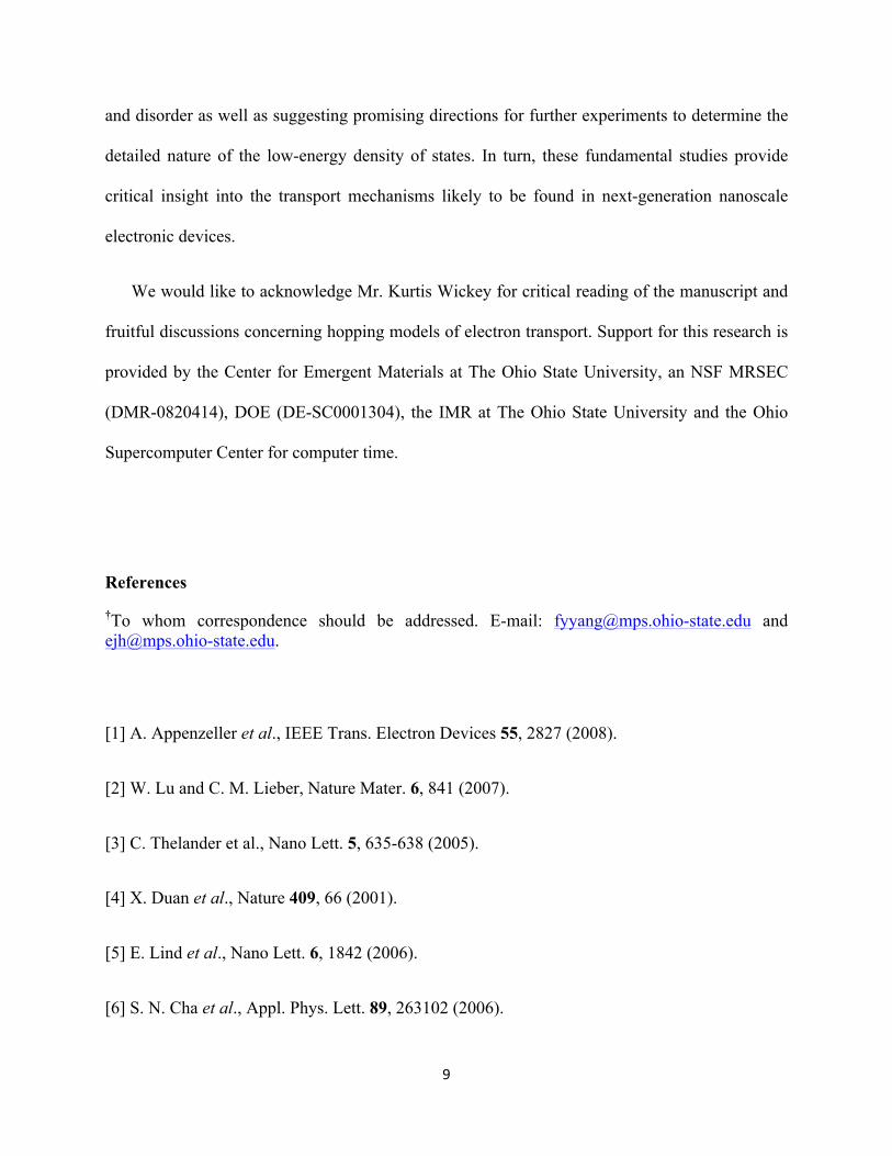
18]). Typical nanowire diameter is 50 ~ 60 nm and typical length is >10 !m. Figure 1 shows
high resolution transmission electron microscopy (HRTEM) images of a representative InP

$""
nanowire. The core is found to have zinc-blende structure with growth along the <111> axis and
an outer oxide shell 2 - 5 nm in thickness.
For electrical measurements, the nanowires are removed from the growth substrate by
sonication in methanol and are dispersed onto a SiO2/Si wafer (300nm/450!m). Isolated high-
quality nanowires are identified using scanning electron microscopy (SEM) and single-wire field
effect transistors are fabricated using standard fabrication techniques (supplemental material 1(b)
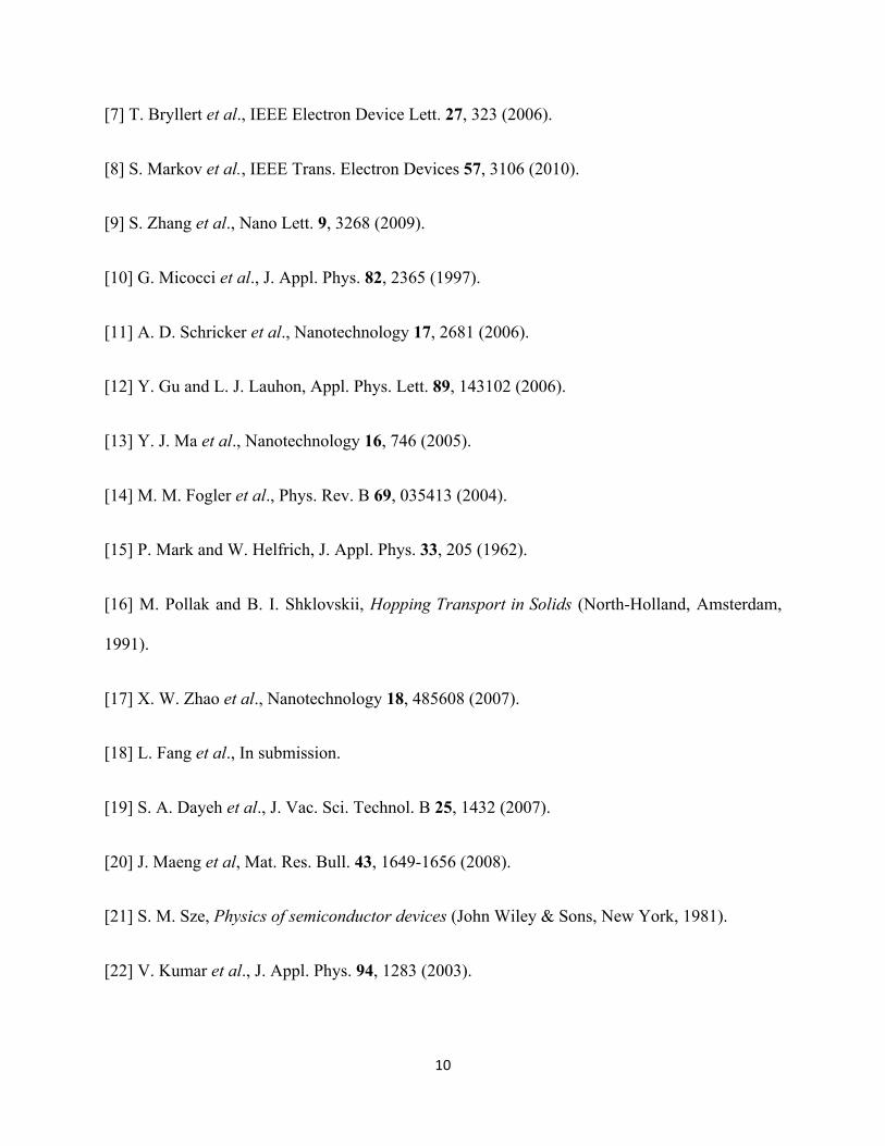
[34]). In Fig. 2, 2-probe and 4-probe current-voltage (I-V) measurements show that the contact
resistance is small compared to the nanowire channel resistance (all subsequent data is collected
in the 4-probe geometry). Despite apparently Ohmic response, the current as a function of gate
voltage, Vg, shows saturation at negative gate voltage and n-type behavior turning on at a
positive gate voltage of approximately +9 V (Fig. 2, bottom right inset). This gate response
stands in contrast to optimized nanowire FET structures that exhibit similar linear I-V curves but
show pinch-off at negative gate voltage with on/off ratios of 104 - 105 [4], but is consistent with
studies of nanowire systems with high trap density [19, 20].
Further evidence for defect-mediated transport can be found in the temperature dependence
of the I-V characteristic at zero gate voltage, Fig. 3(a). The nonlinearity is exacerbated at low
temperature, and quantitative comparison to a Schottky model [21] and plotting on a semi-log
scale (Fig. 3(a), inset) indicate that this nonlinearity is not Schottky in origin. Indeed, the
linearity at high bias seen in log-log plots (Fig. 3(b)) suggests that a power law, rather than the
exponential dependence predicted by the Schottky model, more appropriately describes
electronic transport in these systems.
%""
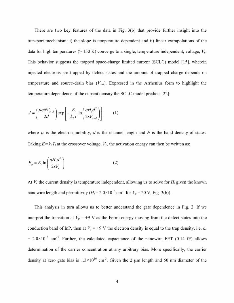
There are two key features of the data in Fig. 3(b) that provide further insight into the
transport mechanism: i) the slope is temperature dependent and ii) linear extrapolations of the
data for high temperatures (> 150 K) converge to a single, temperature independent, voltage, Vc.
This behavior suggests the trapped space-charge limited current (SCLC) model [15], wherein
injected electrons are trapped by defect states and the amount of trapped charge depends on
temperature and source-drain bias (Vs-d). Expressed in the Arrhenius form to highlight the
temperature dependence of the current density the SCLC model predicts [22]:
2
exp ln2 2
s d t t
B s d
qNV E qH dJd k T V
µ!
"
"
# $% &% &= "' () *) *+ , + ,- .
(1)
where µ is the electron mobility, d is the channel length and N is the band density of states.
Taking Et=kBTt at the crossover voltage, Vc, the activation energy can then be written as:
2
ln2
ta t
c
qH dE EV!
" #= $ %
& ' (2)
At Vc the current density is temperature independent, allowing us to solve for Ht given the known
nanowire length and permittivity (Ht = 2.0"1016 cm-3 for Vc = 20 V, Fig. 3(b)).
This analysis in turn allows us to better understand the gate dependence in Fig. 2. If we
interpret the transition at Vg = +9 V as the Fermi energy moving from the defect states into the
conduction band of InP, then at Vg = +9 V the electron density is equal to the trap density, i.e. ne
= 2.0"1016 cm-3. Further, the calculated capacitance of the nanowire FET (0.14 fF) allows
determination of the carrier concentration at any arbitrary bias. More specifically, the carrier
density at zero gate bias is 1.3"1016 cm-3. Given the 2 µm length and 50 nm diameter of the

&""
channel this corresponds to Ne ~ 50 and eN ~ 7 (where Ne is the total number of electrons),
placing these nanowires solidly within the statistical doping regime [8]. This hypothesis is
further supported by the dependence of the SCLC regime on gate voltage. The SCLC model is
valid where band carriers and trap states coexist, and this regime of validity extends to lower Vs-d
and lower temperature as the gate voltage, and consequently ne, increases above Vg = +9 V (the
opposite trend is seen for gate bias decreasing below Vg = +9 V; see Fig. S1 in supplemental
material 2 [34]).
This model implicitly assumes the presence of relatively shallow trap states, i.e. states within
a few times kBT of the conduction band with coupling to the band states. In order to further
assess the plausibility of this assumption, we determine the formation energy of competitive
defects in “bulk” InP from density-functional theory (DFT; calculation of the interface/surface
states would require detailed atomic-scale structural characterization for a realistic picture and is
not considered here). The calculations are performed for supercells with 108 formula units using
the VASP package and potentials [23]; the Generalized-Gradient Approximation (GGA) [24],
cross-checked by the HSE06 hybrid-functional [25]; and a 2!2!2 k-points mesh for the Brillouin
zone integration. Charge states are treated in analogy to Ref. [26]. XPS measurements suggest
that the native oxide on InP is P rich at the interface, and that the oxidation reaction happens at
the surface [27]. Thus, we assume In-rich conditions in the nanowire for determining the
chemical potentials for defect calculations. Using the method of constitutional defects [28], we
find InP-1 and OP
0 to be the most stable defects that also create a trap state near the conduction
band edge. Assuming that the oxidation reaction indeed happens at the surface [27], it is however
less likely that OP0 defects will form (and if they do, are found to form an atomic-like deep level),

'""
leaving InP-1 with a shallow level ~60 meV below the conduction-band edge (see Fig. 3(b), inset)
as a plausible candidate for the trap states identified above [29].
Next, we consider the regime where the SCLC model is not valid, i.e. low Vs-d and low
temperature where the Fermi energy lies in the defect states and hopping transport is expected.
Generally accepted models of hopping transport follow the form [16]:
( )0 0exp mR R T T= (3)
where R0 indicates the overall resistance of the channel, T0 relates to the energy scale of the
hopping transport and m is a constant less than or equal to 1 that indicates the mechanism of the
hopping transport. In order to extract the values of these constants for the InP nanowires studied
here we plot the zero-bias resistance on a log(ln(R)) vs. log(1/T) scale for various gate voltages
(Fig. 4(a)). At zero gate voltage (red-squares) the data reveal two slopes, mhigh = 1.03 ± 0.02 at T
> 158 K and mlow = 0.49 ± 0.02 at T < 158 K. The crossover temperature (158 K at Vg = 0 V)
depends on gate voltage and shifts to lower temperature with increasing positive gate voltage.
For negative gate voltage, the shape of the curve becomes more complex and does not exhibit a
well-defined crossover.
The slopes at Vg = 0 V indicate nearest-neighbor hopping (NNH) and Efros-Shklovskii
variable range hopping (ES-VRH), respectively [30, 31]. The inset in Fig. 4(a) schematically
depicts the crossover between these regimes. At high temperature (kBT greater than the average
variation in trap energy) phonon-assisted hopping allows access to NN hopping sites, as the
temperature decreases the range of energetically accessible hopping sites decreases and VRH
dominates. The energy scale, TNNH, at high temperature is found to be 58 meV (in good
agreement with our DFT calculations of the InP-1 defect), while the energy scale at low
(""
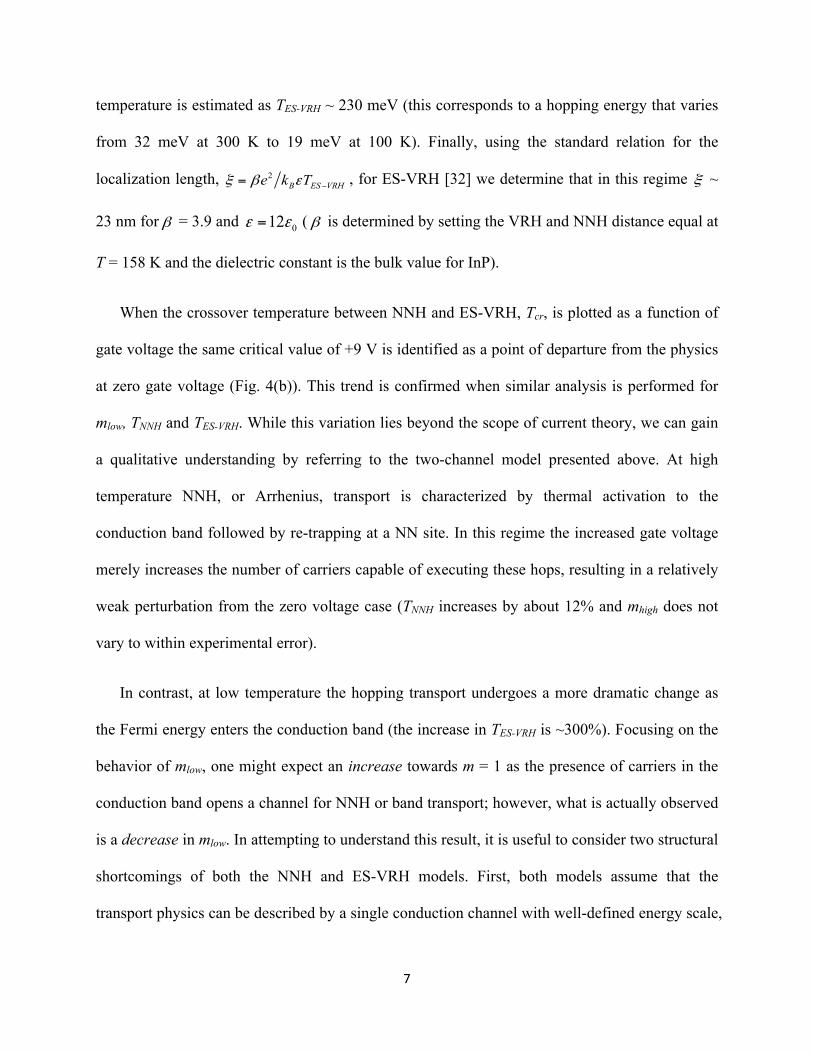
temperature is estimated as TES-VRH ~ 230 meV (this corresponds to a hopping energy that varies
from 32 meV at 300 K to 19 meV at 100 K). Finally, using the standard relation for the
localization length, , for ES-VRH [32] we determine that in this regime ! ~
23 nm for ! = 3.9 and 012! != ( ! is determined by setting the VRH and NNH distance equal at
T = 158 K and the dielectric constant is the bulk value for InP).
When the crossover temperature between NNH and ES-VRH, Tcr, is plotted as a function of
gate voltage the same critical value of +9 V is identified as a point of departure from the physics
at zero gate voltage (Fig. 4(b)). This trend is confirmed when similar analysis is performed for
mlow, TNNH and TES-VRH. While this variation lies beyond the scope of current theory, we can gain
a qualitative understanding by referring to the two-channel model presented above. At high
temperature NNH, or Arrhenius, transport is characterized by thermal activation to the
conduction band followed by re-trapping at a NN site. In this regime the increased gate voltage
merely increases the number of carriers capable of executing these hops, resulting in a relatively
weak perturbation from the zero voltage case (TNNH increases by about 12% and mhigh does not
vary to within experimental error).
In contrast, at low temperature the hopping transport undergoes a more dramatic change as
the Fermi energy enters the conduction band (the increase in TES-VRH is ~300%). Focusing on the
behavior of mlow, one might expect an increase towards m = 1 as the presence of carriers in the
conduction band opens a channel for NNH or band transport; however, what is actually observed
is a decrease in mlow. In attempting to understand this result, it is useful to consider two structural
shortcomings of both the NNH and ES-VRH models. First, both models assume that the
transport physics can be described by a single conduction channel with well-defined energy scale,
2B ES VRHe k T! " # $=

)""
localization length, etc. However, our analysis of the SCLC regime indicates that for Vg > +9 V
both the trap states and the conduction band are occupied. Moreover, while transport through the
defect states proceeds through ES-VRH (as demonstrated by the Vg = 0 V data in Fig. 4(a)),
transport within the conduction band occurs in the presence of a disorder potential defined by the
spatial distribution and occupancy of the trap states. This disorder potential can lead to the
breakup of the conduction band into grains (supplemental material 3 [34], [33]) and at low
temperature and bias likely leads to hopping transport in the conduction band as well. As a result,
a full theoretical description of the transport in this regime needs to account for two parallel
conduction channels that are correlated by the interplay between the trap states and the disorder
potential in the conduction band.
Second, and more generally, the low-temperature low-Vs-d regime is characterized by a
competition between correlation effects and disorder. The average separation between carriers, r0,
is comparable to the thermal deBroglie wavelength for all temperatures considered here (roughly
25 nm and 16 – 27 nm, respectively; supplemental material 4 [34]). As a result, this system is
well into the quantum regime while both NNH and ES-VRH treat electron-electron interactions
classically. The primary effect of these quantum correlations will be to modify the low-energy
density of states, suggesting future studies exploiting tunneling physics to directly probe this
variation.
In conclusion, our comprehensive exploration of defect- and disorder-mediated transport in
semiconducting nanowires reveals a rich interplay between localized trap states, conduction band
transport, quantum effects and electron-electron correlations in the statistical doping regime.
These experimental results provide a foundation for extending current models of hopping
transport to account for multiple conduction channels and the competition between correlation
*""
and disorder as well as suggesting promising directions for further experiments to determine the
detailed nature of the low-energy density of states. In turn, these fundamental studies provide
critical insight into the transport mechanisms likely to be found in next-generation nanoscale
electronic devices.
We would like to acknowledge Mr. Kurtis Wickey for critical reading of the manuscript and
fruitful discussions concerning hopping models of electron transport. Support for this research is
provided by the Center for Emergent Materials at The Ohio State University, an NSF MRSEC
(DMR-0820414), DOE (DE-SC0001304), the IMR at The Ohio State University and the Ohio
Supercomputer Center for computer time.
References
†To whom correspondence should be addressed. E-mail: [email protected] and [email protected].
[1] A. Appenzeller et al., IEEE Trans. Electron Devices 55, 2827 (2008).
[2] W. Lu and C. M. Lieber, Nature Mater. 6, 841 (2007).
[3] C. Thelander et al., Nano Lett. 5, 635-638 (2005).
[4] X. Duan et al., Nature 409, 66 (2001).
[5] E. Lind et al., Nano Lett. 6, 1842 (2006).
[6] S. N. Cha et al., Appl. Phys. Lett. 89, 263102 (2006).
!+""
[7] T. Bryllert et al., IEEE Electron Device Lett. 27, 323 (2006).
[8] S. Markov et al., IEEE Trans. Electron Devices 57, 3106 (2010).
[9] S. Zhang et al., Nano Lett. 9, 3268 (2009).
[10] G. Micocci et al., J. Appl. Phys. 82, 2365 (1997).
[11] A. D. Schricker et al., Nanotechnology 17, 2681 (2006).
[12] Y. Gu and L. J. Lauhon, Appl. Phys. Lett. 89, 143102 (2006).
[13] Y. J. Ma et al., Nanotechnology 16, 746 (2005).
[14] M. M. Fogler et al., Phys. Rev. B 69, 035413 (2004).
[15] P. Mark and W. Helfrich, J. Appl. Phys. 33, 205 (1962).
[16] M. Pollak and B. I. Shklovskii, Hopping Transport in Solids (North-Holland, Amsterdam,
1991).
[17] X. W. Zhao et al., Nanotechnology 18, 485608 (2007).
[18] L. Fang et al., In submission.
[19] S. A. Dayeh et al., J. Vac. Sci. Technol. B 25, 1432 (2007).
[20] J. Maeng et al, Mat. Res. Bull. 43, 1649-1656 (2008).
[21] S. M. Sze, Physics of semiconductor devices (John Wiley & Sons, New York, 1981).
[22] V. Kumar et al., J. Appl. Phys. 94, 1283 (2003).

!!""
[23] G. Kresse and J. Furthmüller, Phys. Rev. B 54, 11169 (1996); P.E. Blöchl, Phys. Rev. B 50,
17953 (1994); G. Kresse, and D. Joubert, Phys. Rev. B 59, 1758 (1999).
[24] J. P. Perdew and Y. Wang, Phys. Rev. B 45, 13244 (1992).
[25] J. Heyd et al., J. Chem. Phys. 118, 8207 (2003); 124, 219906 (2006); J. Paier et al. 124,
154709 (2006).
[26] W. Windl et al., Phys. Rev. Lett. 83, 4345 (1999).
[27] G. Hollinger et al., J. Vac. Sci. Technol. B 5, 1108 (1987).
[28] R. Mishra et al. Chem. Mater. 22, 6092 (2010).
[29] O. D. Restrepo et al., to be published.
[30] A. Yildiz et al., Jpn. J. Appl. Phys. 48, 111203 (2009).
[31] A. L. Efros and B. I. Shklovskii, J. Phys. C 8, L49 (1975).
[32] R. Rosenbaum, Phys. Rev. B 44. 3599 (1991).
[33] I. S. Beloborodov et al., Rev. Mod. Phys. 79, 469 (2007).
[34] See supplemental material at --------- for further experimental conditions and quantitative
analysis.

!#""
FIG. 1. (a) and (b) are high resolution TEM images revealing single crystal structure and a thin
oxide layer (2~5nm) on the surface of the nanowire. (c) Diffraction pattern verifying the zinc-
blende structure of InP nanowire.
FIG. 2. (color online). 2-probe and 4-probe I-V measurements show that contact resistances are
less than 0.05 M#. Left-top inset: SEM image of single nanowire field effect transistor (FET)
device with 4 electrodes. Right bottom inset: I vs. Vg showing saturation current at negative gate
voltage.
FIG. 3. (color online). (a) Temperature dependent I-V plots and fitting to Schottky model
(ideality factor ranges from 97 to 73). Inset is the semi-log plot of showing non-exponential
function dependence on Vs-d. (b) A log-log plot of the same data shows linear behavior, I~VS,
with slope increasing as temperature decreases. The extrapolations of the linear fits converge to a
crossover point (Vc, see text). Inset is a band-structure plot of the InP-1 defect using GGA.
FIG. 4. (color online). (a) Log-log plot of ln(R) vs. 1/T. The graph shows that there is a
crossover in slope: from mhigh = 1.03 at high temperature to mlow = 0.49 at low temperature (Vg =
0 V). Inset is a cartoon showing nearest-neighbor hopping (NNH) at high temperature and ES
variable range hopping (ES-VRH) at low temperature (see text). (b) Red dot is the low
temperature slope deviating from m = 0.5 at Vg > +9 V. Similar gate voltage dependent trends

!$""
can be seen in the crossover temperature (Tcr), NNH temperature (TNNH) and ES-VRH
temperature (TES-VRH) vs. Vg plots.
!%""
FIG.1.
FIG. 2.
!&""
FIG. 3.

!'""
FIG. 4.
!(""
Supplemental material for
Defect states and disorder in charge transport in
semiconductor nanowires
Dongkyun Ko1, X. W. Zhao1, Kongara M. Reddy2, Oscar D. Restrepo2, Rohan Mishra2,
I. S. Beloborodov3, Nandini Trivedi1, Nitin P. Padture2, W. Windl2, F. Y. Yang1
and E. Johnston-Halperin1
1Department of Physics, The Ohio State University, Columbus, Ohio 43210, USA
2Department of Materials Science and Engineering, The Ohio State University, Columbus, Ohio
43210, USA
3Department of Physics and Astronomy, California State University at Northridge, Northridge,
California 91330, USA
Supplemental material 1: Nanowire growth and sample fabrication
a. Nanowire growth
50 nm gold colloid is dispersed onto a silicon substrate as a catalyst for vapor-liquid-solid (VLS)
growth. A 1% Se/InP target is prepared by mixing and pressing InP and In2Se3 polycrystalline
powder. The growth temperature of the substrate is 480ºC and the pressure is controlled at
50~100 Torr with a flow rate of 50 sccm with argon as the carrier gas. A 2 Hz pulsed excimer

!)""
laser with a wavelength of 248 nm and duration of 10 ns is focused on the target to trigger
ablation upstream of the substrate and produces In, P and Se atomic vapors that are subsequently
swept across the growth region. Typical nanowire diameter is 50 ~ 60 nm and length is > 10 !m.
b. Sample fabrication
For electrical measurements, the nanowires are removed from the growth substrate by sonication
in methanol and are dispersed onto a SiO2/Si wafer (300nm/450!m). Isolated high-quality
nanowires are identified using scanning electron microscopy (SEM) and marked using platinum
alignment markers deposited using in situ focused ion beam (FIB) decomposition of an
organometallic precursor (C9H16Pt). Electrical contacts are defined by briefly removing the
sample from the SEM, spin coating poly-methyl methacrylate (PMMA; 4% in anisol), and
reloading into the SEM for electron-beam lithography indexed to the platinum alignment
markers. Metalization consists of an Ohmic stack, Ge/Au/Ni/Au (2nm/20nm/50nm/50nm),
directly after an HCl dip to etch the native oxide shell. Finally, rapid thermal annealing (RTA) in
a forming gas environment is done to reduce contact resistance between the metal stack and the
nanowire.

!*""
Supplemental material 2: Gate dependence of SCLC behaviors
Figs. S1a – S1c show the I-V characteristics of a nanowire FET on a log-log scale for positive
gate voltages. The region of linearity extends to increasingly lower bias and lower temperature as
gate voltage increases and the region of validity for the SCLC model increases (coexistence of
band carriers and traps, see main text). Figs. S1e – S1f show similar plots for negative gate
voltages (all plots have the same current and voltage scale). The region of linearity for these gate
voltage shows opposite behavior trend (shrinking as gate voltage increases in the negative
direction) and pure hopping transport dominates SCLC.

#+""
Fig. S1: (a) – (f) I-V characteristics on log-log scale for different gate voltages. At the largest
negative gate voltage (-30 V, panel (f)) the Fermi energy lies deep in the trap states, far from the
conduction band, and hopping transport dominates at all but the highest temperatures and highest
source-drain bias. As the gate voltage increases towards positive values mixed band- and trap-
mediated transport (the SCLC regime) dominates to increasingly lower temperatures and lower
source-drain bias. At a gate voltage of +30 V (panel (a)) the SCLC regime dominates almost the
entire measurement window. (Panel (d) is the same data as shown in the main text, Fig. 3b)
Supplemental material 3: Absence of Mott-VRH and disorder potential at
conduction band
We expect in highly disordered nanowires Coulomb interactions should dominate at low
temperatures. Mott variable range hopping arises from non-interacting electrons in a random
potential gives an exponent ( )1 1m d= + and equals $ in d=1, whereas ES-VRH that arises in
the classical limit from the combined role of disorder and Coulomb interactions also gives an
exponent of $ independent of dimensionality. However we believe that the physics of these low
dimensional wires is determined by the combined effects of correlations and disorder (see
Supplemental Material 4) and therefore expect that ES-VRH, rather than Mott VRH, dominates
in our samples.
In addition, it is possible that the random distribution of charged traps give rise to a granular
morphology in the conduction band (see main text). Indeed, in granular samples the role of the
Coulomb interaction is strongly enhanced and thus Mott VRH is difficult to observe. This can be

#!""
understood as follows: in semiconductors, the Efros-Shklovskii law may turn to the Mott
behavior with the increase of temperature. This happens when the typical electron energy !
involved in a hopping process becomes larger than the width of the Coulomb gap c! , i.e., when
it falls into the flat region of the density of states where Mott behavior is expected. To estimate
the width of the Coulomb gap c! , one compares the ES expression for the density of states
12 )/()( !"#"
dc
dc e$% , (1)
with the bare density of states 0! i.e., the DOS in the absences of the long-range part of the
Coulomb interactions. Using the condition 0)( !! "#c we obtain
)1/(120
!
""#
$%%&
'=(
d
d
d
ce)* . (2)
Inserting the value for the bare DOS, dcE !" /10 = ( cE is the charging energy for a single grain),
into Eq. (2) we finally obtain
cc E!" . (3)
Equation (3) means that there is no flat region in the density of ground states and, thus, the Mott
regime is difficult to observe in granular wires. To conclude this section we present some
estimates for the Coulomb gap c! and the charging energy cE . The typical grain sizes in our
nanowires are in the range 5 nm < a < 20 nm. These grain sizes are justified by the facts that 1)
our samples are stable meaning that each nanowire has more than one grain in diameter, and 2)
our data clearly show the variable range hopping behavior; this behavior may not hold for a
nanowire with a single grain in diameter. Using these numbers for the charging energies of a

##""
single grain 2cE e a!= we obtain KEK c !!
32 1010<< . The typical dielectric constant ! for
our samples is 3-4 reflecting the fact that our samples are pure conductors. We would like to
point out that the charging energy cE is larger than the characteristic energy hopre !/2 scale
related to the typical electron hop hopr . This is a consequence of the fact that the typical hoping
distance hopr is several times larger than the characteristic size of a single grain arhop > .
Physically this inequality means that an electron propagates through several grains in one hop.
Supplemental material 4: Calculation of r0 and !t
The average separation between carriers (r0) at zero gate voltage can be calculated with the
simple relation:
( )304 13 e
rn
! =
For a typical sample at Vg = 0 V we have ne = 1.3"1016 cm-3 (see main text), giving r0 ~ 25 nm.
At the same time, the thermal deBroglie wave length is given by:
2te B
hm k T
!"
=,
where h is Plank constant, me is the effective mass of electron in InP (me = 0.08"m0) and kB is
Boltzmann’s constant.
In our samples !t varies from 27 nm at T = 100 K to 16 nm at T = 300 K, revealing that these two length scales are comparable even at zero gate potential and the system becomes more quantum
#$""
mechanical with increasing gate voltage (r0 ~ 22 nm at Vg = 9 V). By this simple estimate, our samples exist in the quantum regime for the entire phase spa