Lifetime and leakage current considerations in metal-doped germanium

Germanium Nanowire Synthesis: An Example of Solid-PhaseSeeded Growth with Nickel Nanocrystals
Hsing-Yu Tuan, Doh C. Lee, Tobias Hanrath, and Brian A. Korgel*
Department of Chemical Engineering, Texas Materials Institute,Center for Nano- and Molecular Scienceand Technology, The UniVersity of Texas at Austin, Austin, Texas 78712-1062
ReceiVed June 16, 2005
Germanium nanowires were synthesized by thermal decomposition of diphenyl germane in the presenceof nickel (Ni) nanocrystals in supercritical toluene at 27.8 MPa and temperatures ranging from 410 to460 °C. The growth temperature is well below the lowest Ni-Ge eutectic temperature (762°C), andnanowire crystallization appears to occur by solid-phase alloying of the seed particle. We call this nanowiregrowth mechanism supercritical fluid-solid-solid (SFSS) synthesis.
Introduction
Colloidal routes to nanomaterials synthesis can providehigh-quality nanocrystals and nanowires of metals andsemiconductors that can be dispersed in solvents anddeposited onto substrates or incorporated into polymercomposites for electronic and optical applications.1 However,group IV semiconductors silicon (Si) and germanium (Ge)have been extremely challenging to synthesize in solution,with only marginal success for Si and Ge nanocrystals dueto the difficulties associated with the precursor chemistryand the significant energy barrier to crystallization.2-10 In2000,11 we demonstrated a high-yield crystalline Si nanowiresynthesis in a high-pressure high-temperature organic solventusing diphenylsilane as a Si precursor with Au nanocrystalsto seed and promote Si crystallization and later extended thisapproach to Ge,12 GaAs,13 and GaP14 nanowires. Extensionof the vapor-liquid-solid (VLS) mechanism from the gasphase to organic solvents requires synthetic temperatures
exceeding the Au-Si and Au-Ge eutectic temperature (bothat ∼360°C), which can be achieved in solvents pressurizedabove their critical pointsswe have called this syntheticapproach “supercritical fluid-liquid-solid” (SFLS) growth.15,16
Since Au forms deep electronic traps in Si and Ge, Au-seeded nanowires are relatively undesirable for electronicapplications combining with Si CMOS (complementary-metal-oxide-semiconductor) technology, and other metalswould be preferable as seeds. The challenge facing SFLSGe nanowire growth using alternative metals as seeds is thatthe liquid metal-semiconductor eutectic temperatures ofmost of the more compatible metals with Si CMOS, such asFe, Ni, Ti, and Co, form very high-temperature eutectics withSi and Ge17swell above the decomposition temperatures ofmost organic solvents (for example, 650°C for toluene).18
However, Si and Ge have very highsolid solubility in thesemetals, and metal silicides commonly form by solid-soliddiffusion at relatively low annealing temperatures rangingfrom 400 to 650°C, depending on the material19,20sin therange accessible for supercritical organic solvents.
In a recent Letter, we reported that Ni nanocrystalspromote Si nanowire synthesis in supercritical toluene attemperatures as low as 450°C, which is more than 350°Cbelow the lowest temperature Ni-Si eutectic, and concludedthat Ni nanocrystal-seeded Si nanowire growth can occurby a solid-phaseseeding mechanism from the metal par-ticle.21 Here we provide further evidence supporting theoccurrence of a solid-phase seeding mechanism, showing thatNi nanocrystals promote the formation of high-quality
* Corresponding author. Phone: (512) 471-5633. Fax: (512) 471-7060.E-mail: [email protected].(1) For a recent review, see: Law, M.; Goldberger, J.; Yang, P.Annu.
ReV. Mater. Res.2004, 34, 83-122.(2) Heath, J. R.; LeGoues, F. K.Chem. Phys. Lett.1993, 208, 263-268.(3) Zou, J.; Baldwin, R. K.; Pettigrew, K. A.; Kauzlarich, S. M.Nano
Lett. 2004, 4, 1181-1186.(4) Taylor, B. R.; Fox, G. A.; Hope-Weeks, L. J.; Maxwell, R. S.;
Kauzlarich, S. M.; Lee, H. W. H.Mater. Sci. Eng., B2002, 96, 90-93.
(5) Wilcoxon, J. P.; Samara, G. A.; Provencio, P. N.Phys. ReV. B:Condens. Matter1999, 60, 2704-2714.
(6) Wilcoxon, J. P.; Provencio, P. P.; Samara, G. A.Phys. ReV. B:Condens. Matter2001, 64, 035417.
(7) Holmes, J. D.; Ziegler, K. J.; Doty, R. C.; Pell, L. E.; Johnston, K. P.;Korgel, B. A. J. Am. Chem. Soc.2001, 123, 3743-3748.
(8) Lu, X.; Ziegler, K. J.; Ghezelbash, A.; Johnston, K. P.; Korgel, B. A.Nano Lett.2004, 4, 969-974.
(9) Gerion, D.; Zaitseva, N.; Saw, C.; Casula, M. F.; Fakra, S.; VanBuuren, T.; Galli, G.Nano Lett.2004, 4, 597-602.
(10) Wang, W.; Huang, J.; Ren, Z.Langmuir2005, 21, 751-754.(11) Holmes, J. D.; Johnston, K. P.; Doty, R. C.; Korgel, B. A.Science
2000, 287, 1471-1473.(12) Hanrath, T.; Korgel, B. A.J. Am. Chem. Soc.2002, 124, 1424-1429.(13) Davidson, F. M., III; Schricker, A. D.; Wiacek, R. J.; Korgel, B. A.
AdV. Mater. 2004, 16, 646-649.(14) Davidson, F. M., III; Wiacek, R.; Korgel, B. A.Chem. Mater.2005,
17, 230-233.
(15) Hanrath, T.; Korgel, B. A.AdV. Mater. 2003, 15, 437-440.(16) Shah, P. S.; Hanrath, T.; Johnston, K. P.; Korgel, B. A.J. Phys. Chem.
B 2004, 108, 9574-9587.(17) Thaddeus, B. M.; Hiroaki, O. S. P. R.; Linda, K.Binary Alloy Phase
Diagram, 2nd ed.; ASM Internation: Materials Park, OH, 1990; Vol.1.
(18) Lee, D. C.; Mikulec, F. V.; Korgel, B. A.J. Am. Chem. Soc.2004,126, 4951-4957.
(19) Hsieh, Y. F.; Chen, L. J.; Marshall, E. D.; Lau, S. S.Thin Solid Films1988, 162, 287-294.
(20) Karen, M. M. V. R.Properties of Metal Silicides; Inspec: London,1995.
(21) Tuan, H.-Y.; Lee, D. C.; Hanrath, T.; Korgel, B. A.Nano Lett.2005,5, 681-684.
5705Chem. Mater.2005,17, 5705-5711
10.1021/cm0513031 CCC: $30.25 © 2005 American Chemical SocietyPublished on Web 10/12/2005
crystalline Ge nanowires in organic solvents at growthtemperatures approximately 350°C below the lowest Ni-Ge eutectic temperature. These results are consistent withother recent VLS nanowire growth studies in the gasphase;22,23 for example, Kamins et al., demonstrated Sinanowire synthesis from TiSi2 seeds,22 and Samuelson andco-workers23 have proposed solid-phase seeding of GaAsnanowires from Au nanocrystals under certain conditions.
Here, we present (1) calculations of the expected diameter-dependent melting point depression showing that the Ninanocrystals in the size range used for the Ge nanowiresynthesis should be in the solid phase; (2) evidence that thequality of the nanowires depends sensitively on the NiGex
seed particle diameter with increased extended defectconcentration with increasing diameter, which contrasts withthe case for Au-seeded Ge nanowire synthesis; (3) measure-ments of the nanowire diameter distribution, revealing thatit is shifted to smaller diameters relative to that of the Au-seeded synthesis due to much slower growth of largerdiameter nanowires; (4) measurements of the nanowiregrowth rate, which relates inversely to the nanowire diameter;and (5) estimates of the solid-state diffusion rate that showthat nanowire growth could proceed by either core or surface-enhanced diffusion.
Experimental Details
Ge Nanowire Synthesis.Anhydrous toluene, hexane, andchloroform were purchased from Sigma-Aldrich. Diphenylgermane(DPG) was purchased from Gelest. All chemicals were used asreceived. Organic monolayer-coated Ni nanocrystals 5.6( 0.6 nmin diameter were prepared using established methods.24
Ge nanowires were synthesized in a semibatch 1 mL titaniumgrade-2 high-pressure reactor, heated in a brass block as describedin detail by Hanrath and Korgel.12 An cleaned Si wafer (4× 30mm2) was placed in the reactor to help collect the nanowires. Thereactor was filled with toluene and sealed, then attached to a high-pressure liquid chromatography (HPLC) pump to increase thepressure and control the precursor injection rate. The reactor wasflushed with anhydrous toluene for 3 min at a flow rate of 1.5 mL/min. Prior to precursor injection, the reactor was pressurized withmore anhydrous oxygen-free toluene to a pressure of 3.4 MPa. Then350µL of toluene was injected from a 6-way valve injection loopcontaining 80 mM DPG and Ni nanocrystals at a Ge/Ni mole ratioof 100:1, at a flow rate 0.25 mL/min into the toluene-filled reactorat reaction temperatures ranging from 410 to 460°C. The reactor
was pressurized further with toluene to a final reaction pressure of27.8 MPa. The reaction was kept at temperature for 10 min. Thereactor was then removed from the heating block and allowed tocool to room temperature. The reaction product appears as a darkorange-brown product, which is stored under nitrogen until use.
Characterization Methods. Ge nanowires were characterizedusing high-resolution transmission electron microscopy (HRTEM),high-resolution scanning electron microscopy (HRSEM), andenergy-dispersive X-ray spectroscopy (EDS). HRSEM images wereacquired on a LEO 1530 SEM equipped with a field emission gunoperating between 1 and 5 kV accelerating voltage with workingdistances ranging between 2 and 7 mm. The nanowires were dropcast on silicon substrates for SEM imaging. HRTEM imaging wasperformed on a JEOL 2010F TEM at 200 kV accelerating voltage.The JEOL 2010F is equipped with an Oxford INCA ED spectrom-eter, which was used to acquire EDS data from nanometer-scaleregions in the sample. TEM samples were prepared by drop castingnanowires from chloroform dispersion onto lacey carbon-coatedTEM grids (Electron Microscopy Sciences).
Results
Ge Nanowire Characterization.Figure 1a shows an SEMimage of Ge nanowires obtained by decomposing DPG inthe presence of Ni nanocrystals in toluene at 460°C and23.4 MPa. The nanowires are crystalline Ge with diamondcubic structure with few extended defects, as revealed byextensive TEM images such as those in Figure 2. The averagenanowire length in a preparation is greater than 10µm withdiameters ranging from 5 to 30 nm, with most nanowires inthe 5-15 nm diameter range.
Nanowires could be produced at reaction temperatures aslow as 410°C (Figure 1b), although the product yields dropoff rapidly as the reaction temperature decreases. Thesereaction temperatures are several hundreds of degrees belowthe lowest Ni-Ge eutectic temperature, as seen from thephase diagram in Figure 1c.17 The Ni/Ge mole ratio requiredfor the highest quality Ge nanowires (1:100) is about an orderof magnitude higher than what is needed for Au-seeded SFLSgrowth of Ge nanowires (1:1000) at the same DPG reactionconcentration, and the optimum reaction temperature is∼80°C higher for Ni seeding compared to that for Au seeding.12
The need for these reaction conditions seems to indicateslower nanowire growth kinetics by Ni seeding comparedto that of Au seeding; however, the difference in optimumsynthesis temperature could simply relate to differences inNi/Ge and Au/Ge phase compositions and temperatures, andthe increased DPG decomposition rate at higher temperaturemay simply require a higher metal nanocrystal concentrationto prevent homogeneous Ge particle formation.
The nanowire growth direction was found to be either⟨110⟩ or ⟨111⟩ in approximately equal proportions, with about
(22) Kamins, T. I.; Williams, R. S.; Basile, D. P.; Hesjedal, T.; Harris, J.S. J. Appl. Phys.2001, 89, 1008-1016.
(23) Persson, A. I.; Larsson, M. W.; Stenstroem, S.; Ohlsson, B. J.;Samuelson, L.; Wallenberg, L. R.Nat. Mater.2004, 3, 677-681.
(24) Murray, C. B.; Sun, S.; Doyle, H.; Betley, T.MRS Bull.2001, 26,985-991.
Figure 1. SEM images of Ni nanocrystal-seeded Ge nanowires obtained from 80 mM DPG in toluene at 27.8 MPa and (a) 460°C and (b) 410°C. (c) Thepseudo Ni/Ge phase diagram shows the Ge nanowire synthesis temperature (“Ge nws”; dashed line) 352°C below the lowest eutectic temperature.
5706 Chem. Mater., Vol. 17, No. 23, 2005 Tuan et al.

a 5% occurrence of⟨112⟩ oriented wires (3 of 83 imaged).The TEM images in Figure 2a-c show⟨110⟩ oriented Genanowires with 15.8, 10, and 13.7 nm diameters, and partsd and f in Figure 2 show Ge⟨111⟩ oriented nanowires with12.6, 6.5, and 5.9 nm diameters. The observed 0.325 nm(Figure 2a) and 0.328 nm (Figure 2d) lattice spacings in theTEM images agree with the (111)d-spacing for bulk Ge(0.327 nm). Figure 3 shows a histogram of nanowire growthdirection as a function of diameter obtained from HRTEMimages of 80 nanowires. There is a slightly higher occurrenceof ⟨111⟩ oriented nanowires in the small size range andslightly more ⟨110⟩ oriented wires with diameters greaterthan 15 nm; however, the difference in occurrence ismarginal and does not appear to be statistically significantfor the larger wires. These results sharply contrast SFLS-grown Ge nanowires from Au nanocrystal seeds, which
exhibit ⟨110⟩ growth directions with>90% occurrence,regardless of diameter.25
NiGex Seed Particle Composition.Ni/Ge alloy nano-crystals are found at the tip of most nanowires, as shown inthe example in Figure 4. Nanobeam EDS (Figure 4, parts band c) from the nanowire core shows only Ge, whereas EDSfrom the particle at the tip of the wire shows a mixture ofNi and Ge. EDS measurements of more than 30 NiGex
(25) Hanrath, T.; Korgel, B. A.Small2005, 1, 717-721.
Figure 2. TEM images of Ni nanocrystal-seeded Ge nanowires revealing both (a-c) ⟨110⟩ and (d-f) ⟨111⟩ growth directions that are independent ofdiameter.
Figure 3. Histogram showing the relative occurrence of⟨110⟩ and ⟨111⟩oriented Ge nanowires as a function of diameter.
Figure 4. (a) TEM image of a Ni-Ge alloy seed particle at the end of a14.5 nm Ge nanowire. Nanometer-scale EDS reveals (b) only Ge in thecore of the wire and (c) Ge and Ni in the particle at the nanowire tip. TheCu signal is from background scattering off the copper grid.
Germanium Nanowire Synthesis Chem. Mater., Vol. 17, No. 23, 20055707
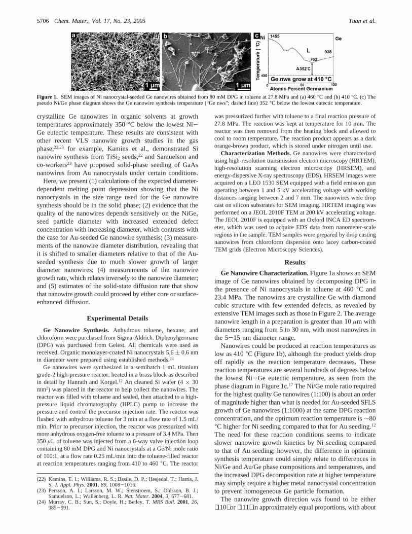
particles found at the tips of nanowires gave NiGex alloycompositions ranging between 1.5< x < 2.8. Metal seedalloying definitely occurs during nanowire synthesis. In allcases where lattice structure could be observed in thenanocrystal at the nanowire tip (the tip needs to be orientedwith the proper zone axis), as in Figure 5, parts a and b, forexample, showing crystalline NiGe2 particles at the tips oftwo Ge nanowires with different growth direction, the crystalstructure (FFT pattern) and lattice spacings matched thoseof orthorhombic NiGe2.26 It is worth noting that there wasno apparent correlation between growth direction and Ni/Ge composition in the seed particle.
Discussion
Melting Point Depression of Ni Nanocrystals.Nano-meter diameter particles (smaller than∼20 nm in diameter)
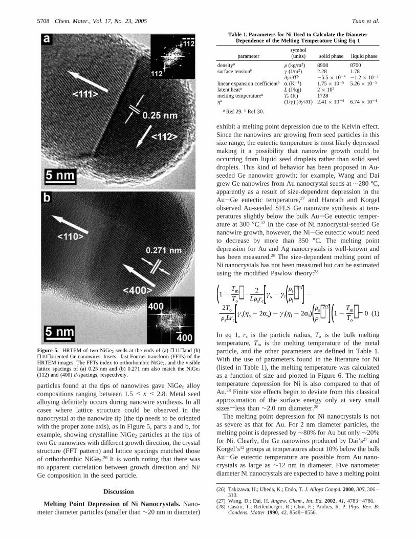
exhibit a melting point depression due to the Kelvin effect.Since the nanowires are growing from seed particles in thissize range, the eutectic temperature is most likely depressedmaking it a possibility that nanowire growth could beoccurring from liquid seed droplets rather than solid seeddroplets. This kind of behavior has been proposed in Au-seeded Ge nanowire growth; for example, Wang and Daigrew Ge nanowires from Au nanocrystal seeds at∼280°C,apparently as a result of size-dependent depression in theAu-Ge eutectic temperature,27 and Hanrath and Korgelobserved Au-seeded SFLS Ge nanowire synthesis at tem-peratures slightly below the bulk Au-Ge eutectic temper-ature at 300°C.12 In the case of Ni nanocrystal-seeded Genanowire growth, however, the Ni-Ge eutectic would needto decrease by more than 350°C. The melting pointdepression for Au and Ag nanocrystals is well-known andhas been measured.28 The size-dependent melting point ofNi nanocrystals has not been measured but can be estimatedusing the modified Pawlow theory:28
In eq 1, rc is the particle radius,To is the bulk meltingtemperature,Tm is the melting temperature of the metalparticle, and the other parameters are defined in Table 1.With the use of parameters found in the literature for Ni(listed in Table 1), the melting temperature was calculatedas a function of size and plotted in Figure 6. The meltingtemperature depression for Ni is also compared to that ofAu.28 Finite size effects begin to deviate from this classicalapproximation of the surface energy only at very smallsizessless than∼2.0 nm diameter.28
The melting point depression for Ni nanocrystals is notas severe as that for Au. For 2 nm diameter particles, themelting point is depressed by∼80% for Au but only∼20%for Ni. Clearly, the Ge nanowires produced by Dai’s27 andKorgel’s12 groups at temperatures about 10% below the bulkAu-Ge eutectic temperature are possible from Au nano-crystals as large as∼12 nm in diameter. Five nanometerdiameter Ni nanocrystals are expected to have a melting point
(26) Takizawa, H.; Uheda, K.; Endo, T.J. Alloys Compd.2000, 305, 306-310.
(27) Wang, D.; Dai, H.Angew. Chem., Int. Ed.2002, 41, 4783-4786.(28) Castro, T.; Reifenberger, R.; Choi, E.; Andres, R. P.Phys. ReV. B:
Condens. Matter1990, 42, 8548-8556.
Figure 5. HRTEM of two NiGe2 seeds at the ends of (a)⟨111⟩ and (b)⟨110⟩ oriented Ge nanowires. Insets: fast Fourier transform (FFTs) of theHRTEM images. The FFTs index to orthorhombic NiGe2, and the visiblelattice spacings of (a) 0.25 nm and (b) 0.271 nm also match the NiGe2
(112) and (400)d-spacings, respectively.
Table 1. Parameters for Ni Used to Calculate the DiameterDependence of the Melting Temperature Using Eq 1
parametersymbol(units) solid phase liquid phase
densitya F (kg/m3) 8908 8700surface tensionb γ (J/m2) 2.28 1.78
∂γ/∂Tb -5.5× 10⁻⁴ -1.2× 10⁻³
linear expansion coefficientb R (K-1) 1.75× 10⁻⁵ 5.26× 10⁻⁵
latent heata L (J/kg) 2× 10⁵
melting temperaturea To (K) 1728ηa (1/γ) (∂γ/∂T) 2.41× 10⁻⁴ 6.74× 10⁻⁴
a Ref 29.b Ref 30.
(1 -Tm
To) - 2
LFsrc[γs - γl(Fs
Fl)2/3] -
2To
FsLrc[γs(ηs - 2Rs) - γl(ηl - 2Rl)(Fs
Fl)2/3](1 -
Tm
To) ) 0 (1)
5708 Chem. Mater., Vol. 17, No. 23, 2005 Tuan et al.
depression of∼10%, which would drop the Ni-Ge eutectictemperature by∼100 °C, which is still over 200°C higherthan the nanowire growth temperature. Furthermore, manyof the nanowires are larger than 10 nm in diameter, whichhave to be growing from seeds with even less of a meltingpoint depression. It is highly unlikely that Ni-seeded Genanowires grow from a liquid alloyed seed droplet at 410 to∼460 °C.
NiGex Seed Particle Shape.The shape of the NiGex
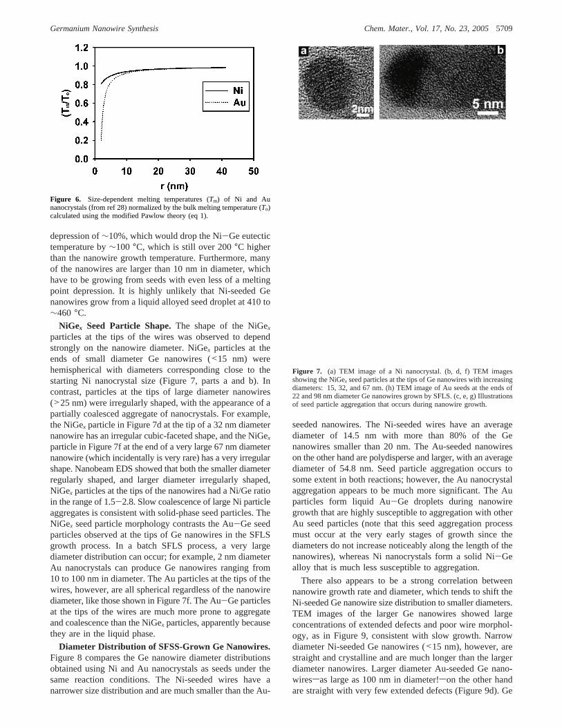
particles at the tips of the wires was observed to dependstrongly on the nanowire diameter. NiGex particles at theends of small diameter Ge nanowires (<15 nm) werehemispherical with diameters corresponding close to thestarting Ni nanocrystal size (Figure 7, parts a and b). Incontrast, particles at the tips of large diameter nanowires(>25 nm) were irregularly shaped, with the appearance of apartially coalesced aggregate of nanocrystals. For example,the NiGex particle in Figure 7d at the tip of a 32 nm diameternanowire has an irregular cubic-faceted shape, and the NiGex
particle in Figure 7f at the end of a very large 67 nm diameternanowire (which incidentally is very rare) has a very irregularshape. Nanobeam EDS showed that both the smaller diameterregularly shaped, and larger diameter irregularly shaped,NiGex particles at the tips of the nanowires had a Ni/Ge ratioin the range of 1.5-2.8. Slow coalescence of large Ni particleaggregates is consistent with solid-phase seed particles. TheNiGex seed particle morphology contrasts the Au-Ge seedparticles observed at the tips of Ge nanowires in the SFLSgrowth process. In a batch SFLS process, a very largediameter distribution can occur; for example, 2 nm diameterAu nanocrystals can produce Ge nanowires ranging from10 to 100 nm in diameter. The Au particles at the tips of thewires, however, are all spherical regardless of the nanowirediameter, like those shown in Figure 7f. The Au-Ge particlesat the tips of the wires are much more prone to aggregateand coalescence than the NiGex particles, apparently becausethey are in the liquid phase.
Diameter Distribution of SFSS-Grown Ge Nanowires.Figure 8 compares the Ge nanowire diameter distributionsobtained using Ni and Au nanocrystals as seeds under thesame reaction conditions. The Ni-seeded wires have anarrower size distribution and are much smaller than the Au-
seeded nanowires. The Ni-seeded wires have an averagediameter of 14.5 nm with more than 80% of the Genanowires smaller than 20 nm. The Au-seeded nanowireson the other hand are polydisperse and larger, with an averagediameter of 54.8 nm. Seed particle aggregation occurs tosome extent in both reactions; however, the Au nanocrystalaggregation appears to be much more significant. The Auparticles form liquid Au-Ge droplets during nanowiregrowth that are highly susceptible to aggregation with otherAu seed particles (note that this seed aggregation processmust occur at the very early stages of growth since thediameters do not increase noticeably along the length of thenanowires), whereas Ni nanocrystals form a solid Ni-Gealloy that is much less susceptible to aggregation.
There also appears to be a strong correlation betweennanowire growth rate and diameter, which tends to shift theNi-seeded Ge nanowire size distribution to smaller diameters.TEM images of the larger Ge nanowires showed largeconcentrations of extended defects and poor wire morphol-ogy, as in Figure 9, consistent with slow growth. Narrowdiameter Ni-seeded Ge nanowires (<15 nm), however, arestraight and crystalline and are much longer than the largerdiameter nanowires. Larger diameter Au-seeded Ge nano-wiressas large as 100 nm in diameter!son the other handare straight with very few extended defects (Figure 9d). Ge
Figure 6. Size-dependent melting temperatures (Tm) of Ni and Aunanocrystals (from ref 28) normalized by the bulk melting temperature (To)calculated using the modified Pawlow theory (eq 1).
Figure 7. (a) TEM image of a Ni nanocrystal. (b, d, f) TEM imagesshowing the NiGex seed particles at the tips of Ge nanowires with increasingdiameters: 15, 32, and 67 nm. (h) TEM image of Au seeds at the ends of22 and 98 nm diameter Ge nanowires grown by SFLS. (c, e, g) Illustrationsof seed particle aggregation that occurs during nanowire growth.
Germanium Nanowire Synthesis Chem. Mater., Vol. 17, No. 23, 20055709

diffusion through a liquid Au-Ge seed is fast, whereas solid-state diffusion limits the nanowire growth rate from NiGe2
seeds when the diameter∼15 nm.
Diffusion-Limited Growth. Several investigators havepredicted for VLS nanowire growth that the growth rateshould decrease as the diameter decreases as a result of theKelvin effect, which lowers the supersaturation in smallerdiameter nanocrystals.31,32Ni-seeded Ge nanowires, however,exhibit slower growth for larger diameter nanowires, indicat-ing that semiconductor diffusion through the metal seedparticle is limiting crystallization. From the observednanowire growth rates, one can estimate a lower limit forthe solid-phase diffusion coefficient of Ge in Ni needed forsolid-phase seeding of the wires. On the basis of the observedlengthsL, obtained from the reactor (consider 10µm with10 min reaction time), the linear growth rate (dL/dt) mustbe at least 1µm/min (0.017µm/s). The Ge flux supplied tothe tip of the solid nanowire surface, Flux|surface, by diffusionthrough the seed metal tip to maintain this growth rate is
whereFGe is the density of Ge. The mass transfer rate at thesolid nanowire surface interfaced with the metal particle can
be estimated as33
wherekm is the mass transfer coefficient (cm/s) and∆CGe,alloy
is the concentration gradient of Ge in the alloyed metal tipfrom the solvent/metal interface to the metal/semiconductorinterface. If nanowire crystallization kinetics are assumedto be much faster than the rate of Ge diffusion through themetal seed particle, then the “free” Ge concentration at themetal/semiconductor interface will be zero. If we assume
(29) CRC Handbook of Chemistry and Physics, 85th ed.; Lide, D. R., Ed.;CRC Press: Boca Raton, FL, 2005.
(30) Murr, E. L. Interfacial Phenomena in Metals and Alloys; Addison-Wesley: Reading, MA, 1975.
(31) Wu, Y.; Fan, R.; Yang, P.Nano Lett.2002, 2, 83-86.(32) Givargizov, E. I.J. Cryst. Growth1975, 31, 20-30.
(33) Bird, R. B.; Stewart, W. E.; Lightfoot., E. N.,Transport Phenomena,2nd ed.; Wiley: New York, 2002.
Figure 8. Diameter distributions of Ge nanowires synthesized in tolueneat 460°C, 23.4 MPa, and a Ge/metal mole ratio of 100:1 using (a) 5.6 nmdiameter Ni nanocrystals and (b) 2 nm diameter Au nanocrystals as seeds.
Figure 9. TEM images of Ge nanowires seeded by (a-c) Ni and (d) Aunanocrystals.
Flux|surface) km∆CGe,alloy
Flux|surface) FGedLdt
5710 Chem. Mater., Vol. 17, No. 23, 2005 Tuan et al.

the highest possible concentration gradient and take the Geconcentration at the metal/solvent interface as the concentra-tion of pure Ge so that∆CGe,alloy ≈ CGe,pure) FGe, then wesee thatkm g(dL/dt) in order to sustain nanowire growth.For simplicity, we can estimatekm for transport to the centerof a sphere of radiusRsphere, which giveskm ) D/Rsphere, whereD is the diffusion coefficient.33 Although the metal seedparticle is not exactly spherical and Ge is diffusing from theseed particle/solvent interface to a flat crystal surface thatcross-sections the sphere, this assumption provides a goodorder of magnitude estimate for mass transfer of Ge fromthe metal/solvent interface to the metal/nanowire interface.Taking the smallest diameter nanowires observed withRsphere
) 2.5 nm, a Ge in Ni diffusivity ofDGefNi g4.25× 10-13
cm2/s is needed to maintain wire growth. This is about 6orders of magnitudefasterthan the measured bulk diffusivityof Ge in Ni at 460°C (DGefNi )1.79 × 10⁻¹⁹ cm2/s).34
HoweVer, the bulk diffusivity ofNi in Ge is extremely fast,with DNifGe ) 1.79× 10⁻⁷ cm2/s.35 As DPG decomposes,Ge adsorbs to the surface of the Ni seed particles, and thenNi can counterdiffuseinto the Ge to promote nanowiregrowth as illustrated in Scheme 1e-h. Another possibilityis a surface-enhanced diffusion process, as shown in Scheme1b-d, in which adsorbed Ge diffuses around the surface ofthe solid Ni nanocrystal to incorporate in the nanowire. Thistype of surface diffusion growth mechanism appears to occurfor Fe nanocrystal-seeded multiwall carbon nanotube growthfrom supercritical toluene18,36 and is a possibility; however,
Ge clearly saturates the Ni seed particle as evidenced by theNiGe2 particles at the tips of the nanowires.
Conclusions
Ni nanocrystals are effective seeds for growing Genanowires at temperatures well below the lowest eutectictemperature on the Ni/Ge phase diagram. Evidence indicatingthat the nanowires grow via a solid-phase seeding processincludes model calculations, which showed that a size-dependent melting temperature depression would not besufficient to induce melting of the NiGex seed particles; asignificant decrease in growth rate with increasing nanowirediameter; and diffusion rates of Ni into Ge that are ordersof magnitude faster than those required for nanowire growth.In contrast to VLS nanowire growth, the slower growth ratesfor larger diameter wires focuses the diameter distributionto smaller sizes. In VLS growth, careful control of theprocessing parameters is needed to maintain a narrowdiameter distribution,16 and this represents one potentialadvantage of SFSS over SFLS. The wide range of alternativemetals with high Si and Ge solubility makes SFSS apromising route for greatly increasing the number of metalsavailable for seeded semiconductor nanowire growth at lowerthan expected processing temperatures, which is an importantfactor in the future integration of nanowires in devices.
Acknowledgment. We thank the National Science Founda-tion, the Welch Foundation, and the Advanced MaterialsResearch Center in collaboration with International SEMAT-ECH for financial support of this research. We also thank J. P.Zhou for TEM assistance.
CM0513031
(34) Mantl, S.; Rothman, S. J.; Nowicki, L. J.; Lerner, J. L.J. Phys. F:Met. Phys.1983, 13, 1441-14488.
(35) Goldsmid, H. J.Diffusion in Semiconductors; Inspec: London, 1963.(36) Lee, D. C.; Korgel, B. A.Mol. Simul., 2005, 31, 637-642.
Scheme 1. Schematic of Two Possible Mechanisms for SFSS Growtha
a Steps b-d: surface-enhanced solid-state diffusion process. Steps e-h: solid-state volume counterdiffusion process.
Germanium Nanowire Synthesis Chem. Mater., Vol. 17, No. 23, 20055711
Copyright © 2022 FDOKUMEN