
Preparation of the Ge(001) surface towards fabrication of atomic-scale germanium devices
8
Preparation of the Ge(001) surface towards fabrication of atomic-scale germanium devices This article has been downloaded from IOPscience. Please scroll down to see the full text article. 2011 Nanotechnology 22 145604 (http://iopscience.iop.org/0957-4484/22/14/145604) Download details: IP Address: 129.94.141.125 The article was downloaded on 29/03/2011 at 08:48 Please note that terms and conditions apply. View the table of contents for this issue, or go to the journal homepage for more Home Search Collections Journals About Contact us My IOPscience
Transcript of Preparation of the Ge(001) surface towards fabrication of atomic-scale germanium devices

Preparation of the Ge(001) surface towards fabrication of atomic-scale germanium devices
This article has been downloaded from IOPscience. Please scroll down to see the full text article.
2011 Nanotechnology 22 145604
(http://iopscience.iop.org/0957-4484/22/14/145604)
Download details:
IP Address: 129.94.141.125
The article was downloaded on 29/03/2011 at 08:48
Please note that terms and conditions apply.
View the table of contents for this issue, or go to the journal homepage for more
Home Search Collections Journals About Contact us My IOPscience
IOP PUBLISHING NANOTECHNOLOGY
Nanotechnology 22 (2011) 145604 (7pp) doi:10.1088/0957-4484/22/14/145604
Preparation of the Ge(001) surfacetowards fabrication of atomic-scalegermanium devicesW M Klesse1, G Scappucci1,2, G Capellini3 and M Y Simmons1,2
1 School of Physics, University of New South Wales, Sydney, NSW 2052, Australia2 Australian Research Council Centre of Excellence for Quantum Computing andCommunication Technology, University of New South Wales, Sydney, NSW 2052, Australia3 Dipartimento di Fisica, Universita di Roma Tre, Via della Vasca Navale 84, 00146 Roma,Italy
E-mail: [email protected] and [email protected]
Received 30 November 2010Published 3 March 2011Online at stacks.iop.org/Nano/22/145604
AbstractWe demonstrate the preparation of a clean Ge(001) surface with minimal roughness(RMS ∼ 0.6 A), low defect densities (∼0.2% ML) and wide mono-atomic terraces(∼80–100 nm). We use an ex situ wet chemical process combined with an in situ annealtreatment followed by a homoepitaxial buffer layer grown by molecular beam epitaxy and asubsequent final thermal anneal. Using scanning tunneling microscopy, we investigate the effecton the surface morphology of using different chemical reagents, concentrations as well assubstrate temperature during growth. Such a high quality Ge(001) surface enables the formationof defect-free H-terminated Ge surfaces for subsequent patterning of atomic-scale devices byscanning tunneling lithography. We have achieved atomic-scale dangling bond wire structures1.6 nm wide and 40 nm long as well as large, micron-size patterns with clear contrast oflithography in STM images.
(Some figures in this article are in colour only in the electronic version)
1. Introduction
As electronic device miniaturization to and beyond the 16 nmnode foresees the replacement of the Si channel in transistorswith higher mobility materials [1, 2], there is growing interestin the realization of Ge-based devices and devices developedat the atomic scale [3]. This renewed interest stems from thedevelopment of high-κ dielectrics compatible with Ge [2], andthe integration of Ge onto silicon substrates [4] which helpto circumvent the issues of a lack of high quality native gatedielectric and the costs of high purity Ge substrates. There hasalso been a growing interest in the development of atomic-scaledevices, such as nanowires [5], single electron transistors [6]and few electron quantum dots [7], using scanning tunnelingmicroscopy (STM) lithography and molecular beam epitaxy(MBE) to induce deterministic placement of dopants insemiconductor crystals [8–10]. Typically, an STM tip isused to locally remove H atoms from a hydrogen-terminated
semiconductor surface, to create an atomic template foradsorption and incorporation of dopants within the patternedareas. We have recently adapted this approach for thefabrication of atomic-scale devices in Ge, demonstrating twokey milestones of the process: (i) the fabrication of P δ-layers in Ge with minimal dopant redistribution and highelectrical activation [11, 12], and (ii) atomic-scale lithographyon Ge(001) surfaces by UHV-STM [13].
The first step of all atomic-scale fabrication processesis the preparation of a defect free, atomically flat Ge(001)surface. Minimization of the defect density is criticalto obtain a uniform H-termination of the surface and—consequently—successful doping within the H-depassivatedareas. In addition, the starting surface should compriselarge terraces with minimal roughness to clearly identifylithographic patterns during STM imaging and accuratelyevaluate their quality. Since the contrast of the H-lithographyin STM images is given by the height of Ge dangling bonds
0957-4484/11/145604+07$33.00 © 2011 IOP Publishing Ltd Printed in the UK & the USA1
Nanotechnology 22 (2011) 145604 W M Klesse et al
on the H-terminated Ge(001) surface (0.8 A), the roughness ofthe starting Ge surface should be at most of the same order ofmagnitude measured over the length scale of the lithographicpatterns, which typically ranges from the nano- to the micro-scale. So far, two different approaches have been investigatedfor UHV-based cleaning of Ge(001): the first relies on anex situ wet etching/oxidation process followed by an in situthermal anneal [14–19]; the second is based on in situ ionsputtering/annealing cycles [19–22] eventually followed byGe epitaxy to cure the surface from the ion bombardmentdamage [19, 23]. The achievement of clean, defect-freeGe(001) surfaces has proved difficult with the first approachowing to the poor quality of the substoichiometric GeOx oxidewhich does not protect the Ge from contamination. The secondmethod, instead, relies on aggressive sputtering of the surfaceuntil any contaminant is removed, and has produced so far thebest results. Indeed, the majority of atomic-scale STM studieson the Ge(001) surface have been on surfaces prepared by theion-sputtering-based process [22].
In this paper we demonstrate that it is also possibleto prepare a clean, atomically flat, and defect-free Ge(001)surface starting with an ex situ wet etching/oxidation process—thereby avoiding any ion sputtering procedure—provided thata Ge buffer layer is grown followed by an in situ thermalanneal.
Our surface preparation process comprises four steps:(i) repeated ex situ wet chemical etching/oxidation is meantto strip/reform a GeOx passivation layer which will then be(ii) thermally desorbed in situ. We compared two differentetching agents (HF and HCl) and varied the concentration ofthe oxidation agent (H2O2), to minimize surface defect densityand roughness. After this cleaning procedure, in order tofurther improve the surface quality, (iii) we deposited bufferlayers of intrinsic Ge followed by (iv) a second thermal anneal.We found that the buffer layer/thermal anneal is the key step inthe process to achieve a defect-free surface with large terracessuitable for future atomic-scale Ge device fabrication. On theprepared defect-free surface with large terraces we demonstrateclear contrast of the H-lithography in STM images on boththe atomic and large micron scales, a key milestone towardsatomic-scale fabrication in Ge by STM.
2. Experimental details
All experiments were carried out in a UHV combinedSTM/MBE system with a base pressure below 5×10⁻¹¹ mbar.The Ge(001) substrates were cleaved from Sb-doped Ge(001)4 inch wafers (resistivity of 1–10 � cm). Ex situ cleaningwas performed in a clean-room ambient using electronic gradeisopropanol, hydrofluoric acid, hydrochloric acid, hydrogenperoxide and deionized water (resistivity of 20 M� cm).
To optimize the ex situ wet chemical treatment, weperformed a series of experiments on different samples (C1–C4) in which we investigated the use of two etching agents(HF and HCl) and varied the concentration of the oxidizingagent (H2O2). Table 1 gives an overview of the experimentalparameters we varied for each sample. The samples weredegreased by isopropanol in ultrasound for 5 min and then
Table 1. Ex situ and in situ preparation procedures for the sevenGe(001) samples studied. In samples C1–C4 we optimized the ex situwet chemical treatment by investigating the use of two etching agents(HF and HCl) and varying the concentration of the oxidizing agent(H2O2). In samples B1–B3 we investigated the effect of depositingin situ a Ge buffer layer at increasing substrate temperatures followedby a thermal anneal.
Etch Oxidation Buffer layer Anneal
Sample HF (%) HCl (%) H2O2 (%) Tg (◦C) (◦C)
C1 10 — 30 — —C2 — 36 30 — —C3 — 36 10 — —C4 — 36 7 — —B1 — 36 7 450 760B2 — 36 7 500 760B3 — 36 7 600 760
stripped of their native oxide by dipping for 60 s in etchingsolutions of HF:H2O 10:100 (sample C1) or HCl:H2O 36:100(samples C2–C4). A passivation oxide was then chemicallygrown by dipping for 30 s in a H2O2:H2O bath. Theconcentration of the H2O2 in the oxidizing solution wasreduced in the different experiments from 30% (samples C1and C2) to 10% (sample C3) and 7% (sample C4). For eachsample the process of stripping/reforming a passivation oxidewas repeated four times. The length of each additional etchingstep was reduced to 45 s and that of the final oxidation stepextended to 60 s. Immediately after the ex situ treatment,the samples were loaded into the UHV system through a fastentry lock for the in situ cleaning process. The substrateJoule heating in the UHV system was achieved by flowinga DC current directly through the substrate. The in situcleaning process was the same for all samples and consistedof outgassing at 250 ◦C for ∼1 h followed by a flash annealat 760 ± 10 ◦C for 60 s to remove the GeOx passivation layer,fast cooling to 600 ◦C and a slow cooling from 600 ◦C to roomtemperature at ∼2 ◦C s−1 to obtain an ordered reconstructedsurface, as observed by STM. The maximum pressure duringthe flash annealing was below 8 × 10⁻⁹ mbar.
Having optimized the ex situ wet chemical treatment, weinvestigated the effect of depositing in situ a Ge buffer layerat increasing substrate temperatures from 450 (sample B1) to500 ◦C (sample B2) and 600 ◦C (sample B3). This is the criticalgrowth temperature range expected to have a major impact onsurface roughness, since Ge homoepitaxy changes from island-like to step-flow growth mode, as we previously observed [12].Finally, we investigated for all three samples B1–B3 the effectof a post-growth flash anneal to 760 ◦C. For Ge buffer layerdeposition, the samples were transferred in UHV into an MBEchamber where epitaxial layers of intrinsic Ge were grown at arate of 0.13 A s−1. The substrate temperatures during epitaxywere measured by means of a thermocouple mounted near thesample holder. The surface morphology was characterized ateach step of the process by STM imaging at room temperaturewith a sample bias between −1.0 and −1.6 V and a tunnelingcurrent in the 0.4–1.0 nA range. A detailed description of thein situ H-termination process of the Ge(001) surface and STMH-lithography is provided in [13].
2
Nanotechnology 22 (2011) 145604 W M Klesse et al
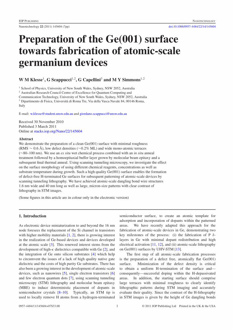
Figure 1. (a) Optimization of the ex situ cleaning procedure for minimizing the surface roughness. See text for details. ((b), (c)) Filled-stateSTM images at different length scales (400 × 400 nm2 (b), 20 × 20 nm2 (c)) of the prepared Ge(001) surface of sample C4.
3. Results and discussion
3.1. Optimization of ex situ chemical passivation/in situthermal anneal
In figure 1(a) we plot the root mean square (RMS) roughnessaveraged on several 400×400 nm2 areas of the surface for eachof the C1–C4 samples by STM image analysis. A comparisonbetween samples C1 and C2 indicates that a fluorine-based wetetch (sample C1) produces a rougher surface with an averageRMS roughness of ∼10 A. This roughness is reduced by afactor ∼5 to 1.95 A by using a chlorine-based wet etch (sampleC2), in agreement with AFM analysis [24] where a HF-treatedGe(001) surface showed a higher roughness (∼6 A) comparedto a HCl-treated Ge(001) surface (∼2.9 A). This dependencein surface roughness was attributed to the etching mechanismin the case of HF which leads to Ge back-bond breaking.Decreasing the H2O2 concentration in the oxidizing solution(samples C3 and C4) however was also observed to bringabout a monotonic decrease of the RMS surface roughnessto a value of 1.1 A, saturating for sample C4 with the lowestconcentration of H2O2.
In figures 1(b) and (c) we show large, atomic-scale STMimages of the optimized surface for sample C4 after the in situflash anneal. As expected for the Ge(001) surface [22], weobserve mono-atomic terraces with a broad width distributionand irregular oriented step-edges (figure 1(b)), with (2 × 1)
dimer rows, as well as regions of higher order c(4 × 2)
and p(2 × 2) reconstruction due to in-phase and out-of-phase buckling of surface dimers on adjacent dimer rows(figure 1(c)). The defects on the surface reconstruction aremainly made of missing dimer rows with a density of ∼2% ofa monolayer (1 ML = 6.25 × 10¹⁴ atoms cm−2). Moreoverwe observe the presence of randomly distributed relativelylarge features with a typical area of 3 × 3 nm2 and anapparent height of up to ∼5 A (figures 1(b) and (c)). Thesestructures are usually surrounded by pits on the surface, asshown in the close-up, figure 1(c). Similar features havebeen previously observed on Ge(001) and related to carboncontamination [14, 17, 21, 25]. We argue that the featuresare more likely Ge ‘flakes’ (clusters of Ge atoms) formedduring the in situ high-temperature flash anneal: the thermaldesorption of the GeOx layer rips off small clusters of Geatoms from the surface that can locally redeposit to form aGe cluster with a nearby pit. To support this interpretationwe point out three interesting observations: (i) these featuresare not associated with any pinning of surface steps, ascommonly observed with carbon contamination; (ii) they donot act as heterogeneous nucleation sites for structural defectsduring subsequent Ge MBE growth [11]; in particular, as alsoobserved by other groups [17, 21], they are not associatedto any pit formation during Ge encapsulation. Moreover,(iii) we found that the density of these clusters on the surfaceis decreased by imaging with the STM under high sample
3

Nanotechnology 22 (2011) 145604 W M Klesse et al
Figure 2. Filled-state STM images (250 × 250 nm2) of the surface morphology directly after 25 nm buffer layer growth at (a) 450 ◦C,(b) 500 ◦C, and (c) 600 ◦C, with the insets showing atomic resolution close-ups (20 × 20 nm2). (d)–(f) Each of these surfaces after the thermalanneal to 760 ◦C. (g) RMS roughness versus buffer layer growth temperature measured on several 400 × 400 nm2 STM images of samplesB1–B3 before (circle) and after (open square) the final anneal step. The dotted line is a reference for the roughness before buffer layer growth.
4
Nanotechnology 22 (2011) 145604 W M Klesse et al
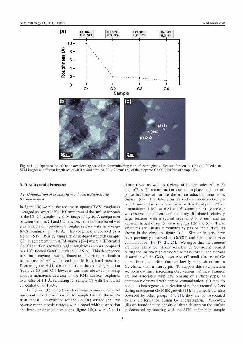
Figure 3. Filled-state, atomic resolution STM images (25 × 25 nm2) of samples B1 (a), B2 (b) and B3 (c) after the final anneal. (d) Missingdimer defect density for samples B1–B3 before (circle) and after (open square) the final anneal step. The dotted line is a reference for thedefect density before buffer layer growth.
bias/tunneling current conditions. The annihilation of small Geclusters has also been observed previously [26] and attributedto the interaction between the STM tip and the Ge(001) surface,thereby supporting our interpretation.
3.2. Growth and thermal anneal of a Ge buffer layer
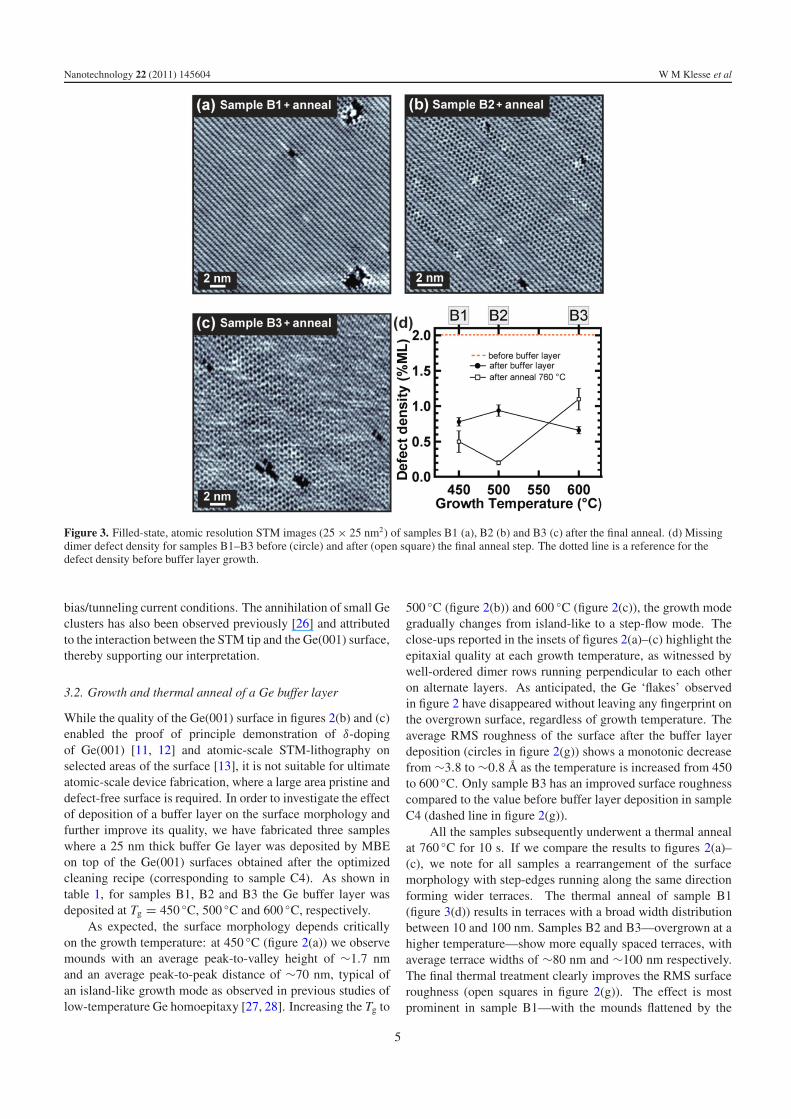
While the quality of the Ge(001) surface in figures 2(b) and (c)enabled the proof of principle demonstration of δ-dopingof Ge(001) [11, 12] and atomic-scale STM-lithography onselected areas of the surface [13], it is not suitable for ultimateatomic-scale device fabrication, where a large area pristine anddefect-free surface is required. In order to investigate the effectof deposition of a buffer layer on the surface morphology andfurther improve its quality, we have fabricated three sampleswhere a 25 nm thick buffer Ge layer was deposited by MBEon top of the Ge(001) surfaces obtained after the optimizedcleaning recipe (corresponding to sample C4). As shown intable 1, for samples B1, B2 and B3 the Ge buffer layer wasdeposited at Tg = 450 ◦C, 500 ◦C and 600 ◦C, respectively.
As expected, the surface morphology depends criticallyon the growth temperature: at 450 ◦C (figure 2(a)) we observemounds with an average peak-to-valley height of ∼1.7 nmand an average peak-to-peak distance of ∼70 nm, typical ofan island-like growth mode as observed in previous studies oflow-temperature Ge homoepitaxy [27, 28]. Increasing the Tg to
500 ◦C (figure 2(b)) and 600 ◦C (figure 2(c)), the growth modegradually changes from island-like to a step-flow mode. Theclose-ups reported in the insets of figures 2(a)–(c) highlight theepitaxial quality at each growth temperature, as witnessed bywell-ordered dimer rows running perpendicular to each otheron alternate layers. As anticipated, the Ge ‘flakes’ observedin figure 2 have disappeared without leaving any fingerprint onthe overgrown surface, regardless of growth temperature. Theaverage RMS roughness of the surface after the buffer layerdeposition (circles in figure 2(g)) shows a monotonic decreasefrom ∼3.8 to ∼0.8 A as the temperature is increased from 450to 600 ◦C. Only sample B3 has an improved surface roughnesscompared to the value before buffer layer deposition in sampleC4 (dashed line in figure 2(g)).
All the samples subsequently underwent a thermal annealat 760 ◦C for 10 s. If we compare the results to figures 2(a)–(c), we note for all samples a rearrangement of the surfacemorphology with step-edges running along the same directionforming wider terraces. The thermal anneal of sample B1(figure 3(d)) results in terraces with a broad width distributionbetween 10 and 100 nm. Samples B2 and B3—overgrown at ahigher temperature—show more equally spaced terraces, withaverage terrace widths of ∼80 nm and ∼100 nm respectively.The final thermal treatment clearly improves the RMS surfaceroughness (open squares in figure 2(g)). The effect is mostprominent in sample B1—with the mounds flattened by the
5
Nanotechnology 22 (2011) 145604 W M Klesse et al
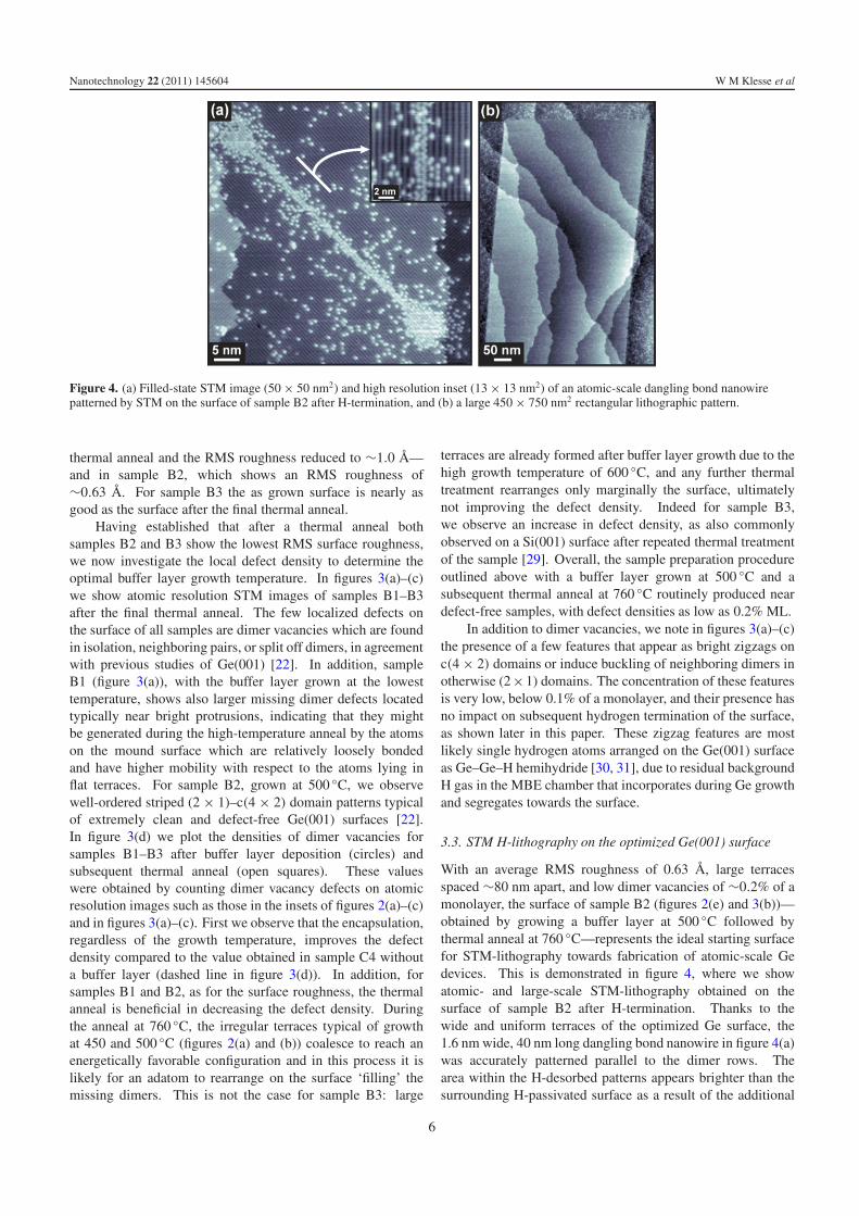
Figure 4. (a) Filled-state STM image (50 × 50 nm2) and high resolution inset (13 × 13 nm2) of an atomic-scale dangling bond nanowirepatterned by STM on the surface of sample B2 after H-termination, and (b) a large 450 × 750 nm2 rectangular lithographic pattern.
thermal anneal and the RMS roughness reduced to ∼1.0 A—and in sample B2, which shows an RMS roughness of∼0.63 A. For sample B3 the as grown surface is nearly asgood as the surface after the final thermal anneal.
Having established that after a thermal anneal bothsamples B2 and B3 show the lowest RMS surface roughness,we now investigate the local defect density to determine theoptimal buffer layer growth temperature. In figures 3(a)–(c)we show atomic resolution STM images of samples B1–B3after the final thermal anneal. The few localized defects onthe surface of all samples are dimer vacancies which are foundin isolation, neighboring pairs, or split off dimers, in agreementwith previous studies of Ge(001) [22]. In addition, sampleB1 (figure 3(a)), with the buffer layer grown at the lowesttemperature, shows also larger missing dimer defects locatedtypically near bright protrusions, indicating that they mightbe generated during the high-temperature anneal by the atomson the mound surface which are relatively loosely bondedand have higher mobility with respect to the atoms lying inflat terraces. For sample B2, grown at 500 ◦C, we observewell-ordered striped (2 × 1)–c(4 × 2) domain patterns typicalof extremely clean and defect-free Ge(001) surfaces [22].In figure 3(d) we plot the densities of dimer vacancies forsamples B1–B3 after buffer layer deposition (circles) andsubsequent thermal anneal (open squares). These valueswere obtained by counting dimer vacancy defects on atomicresolution images such as those in the insets of figures 2(a)–(c)and in figures 3(a)–(c). First we observe that the encapsulation,regardless of the growth temperature, improves the defectdensity compared to the value obtained in sample C4 withouta buffer layer (dashed line in figure 3(d)). In addition, forsamples B1 and B2, as for the surface roughness, the thermalanneal is beneficial in decreasing the defect density. Duringthe anneal at 760 ◦C, the irregular terraces typical of growthat 450 and 500 ◦C (figures 2(a) and (b)) coalesce to reach anenergetically favorable configuration and in this process it islikely for an adatom to rearrange on the surface ‘filling’ themissing dimers. This is not the case for sample B3: large
terraces are already formed after buffer layer growth due to thehigh growth temperature of 600 ◦C, and any further thermaltreatment rearranges only marginally the surface, ultimatelynot improving the defect density. Indeed for sample B3,we observe an increase in defect density, as also commonlyobserved on a Si(001) surface after repeated thermal treatmentof the sample [29]. Overall, the sample preparation procedureoutlined above with a buffer layer grown at 500 ◦C and asubsequent thermal anneal at 760 ◦C routinely produced neardefect-free samples, with defect densities as low as 0.2% ML.
In addition to dimer vacancies, we note in figures 3(a)–(c)the presence of a few features that appear as bright zigzags onc(4 × 2) domains or induce buckling of neighboring dimers inotherwise (2×1) domains. The concentration of these featuresis very low, below 0.1% of a monolayer, and their presence hasno impact on subsequent hydrogen termination of the surface,as shown later in this paper. These zigzag features are mostlikely single hydrogen atoms arranged on the Ge(001) surfaceas Ge–Ge–H hemihydride [30, 31], due to residual backgroundH gas in the MBE chamber that incorporates during Ge growthand segregates towards the surface.
3.3. STM H-lithography on the optimized Ge(001) surface
With an average RMS roughness of 0.63 A, large terracesspaced ∼80 nm apart, and low dimer vacancies of ∼0.2% of amonolayer, the surface of sample B2 (figures 2(e) and 3(b))—obtained by growing a buffer layer at 500 ◦C followed bythermal anneal at 760 ◦C—represents the ideal starting surfacefor STM-lithography towards fabrication of atomic-scale Gedevices. This is demonstrated in figure 4, where we showatomic- and large-scale STM-lithography obtained on thesurface of sample B2 after H-termination. Thanks to thewide and uniform terraces of the optimized Ge surface, the1.6 nm wide, 40 nm long dangling bond nanowire in figure 4(a)was accurately patterned parallel to the dimer rows. Thearea within the H-desorbed patterns appears brighter than thesurrounding H-passivated surface as a result of the additional
6
Nanotechnology 22 (2011) 145604 W M Klesse et al
tunnel current of the Ge surface states. A close-up of a segmentof the two dimer row wide nanowire is shown as an insetin figure 4(a). Within the desorbed surface we observe thetypical buckling as a fingerprint of the clean Ge(001) surfacein contrast with the (2×1) reconstructed monohydride surface.The bright protrusions which are randomly distributed overthe STM image are single dangling bonds due to imperfectH-passivation of the Ge(001) surface. Note that not onesingle defect is present along the dangling bond nanowire, aclear improvement compared to previously published imagesof STM-lithography on Ge(001) [13]. The advantage ofhaving large terraces with low surface roughness is highlightedin figure 4(b), which shows an STM image of a large450 × 750 nm2 rectangular lithographic pattern. Comparedto previously published large-scale lithographic patterns [13],there is a clear contrast in the image with a sharp edge betweenthe patterned and H-terminated Ge(001) surface regions and,most of all, there are no Ge clusters on the surface.
4. Conclusions
In summary, we have developed and optimized a processfor the preparation of atomically flat, clean and defect-freeGe(001) surfaces suitable for future atomic-scale Ge devicefabrication. This process combines an ex situ wet chemicalcleaning treatment using HCl:H2O (36:100) and H2O2:H2O(7:100) to alternately strip and reform a GeOx passivationlayer, with an in situ cleaning treatment which involvesa controlled in situ thermal desorption of the oxide layerfollowed by a Ge buffer layer growth and a subsequent finalthermal anneal. By growing a 25 nm thick buffer layer at500 ◦C by MBE and subsequent thermal anneal at 760 ◦Cwe obtain clean Ge(001) surfaces with single layer step-edges forming wide terraces and surface defect densities below0.2% ML. The high quality of the optimized surface allowsatomically precise STM-lithography, a key fabrication steptowards future atomic-scale germanium devices.
Acknowledgments
WMK acknowledges support from Zyvex Labs. GS ac-knowledges support from UNSW under the 2010 ScienceFaculty Research Grant scheme. GC is thankful to UNSWfor a Visiting Professor Fellowship. MYS acknowledges anAustralian Government Federation Fellowship.
References
[1] Shang H, Frank M M, Gusev E P, Chu J O, Bedell S W,Guarini K W and Ieong M 2006 IBM J. Res. Dev. 50 377–86
[2] Kamata Y 2008 Mater. Today 11 30–8[3] Zhirnov V V, Cavin R K, Herr D J C and Wooldridge T A 2002
IEEE Trans. Semicond. Manuf. 15 157–68[4] Masini G, Sahni S, Capellini G, Witzens J and Gunn C 2008
Adv. Opt. Technol. 2008 196572[5] Rueß F J, Goh K E J, Butcher M J, Reusch T C G, Oberbeck L,
Weber B, Hamilton A R and Simmons M Y 2007Nanotechnology 18 044023
[6] Fuhrer A, Fuechsle M, Reusch T C G, Weber B andSimmons M Y 2009 Nano Lett. 9 707–10
[7] Fuechsle M, Mahapatra S, Zwanenburg F A, Friesen M,Eriksson M A and Simmons M Y 2010 Nat. Nanotechnol.5 502–5
[8] Lyding J W, Shen T C, Hubacek J S, Tucker J R and Abeln G C1994 Appl. Phys. Lett. 64 2010–2
[9] Tucker J R and Shen T C 1998 Solid-State Electron. 42 1061–7[10] Ruess F J, Oberbeck L, Simmons M Y, Goh K E J,
Hamilton A R, Hallam T, Schofield S R, Curson N J andClark R G 2004 Nano Lett. 4 1969–73
[11] Scappucci G, Capellini G, Lee W C T and Simmons M Y 2009Appl. Phys. Lett. 94 162106
[12] Scappucci G, Capellini G and Simmons M Y 2009 Phys. Rev. B80 233202
[13] Scappucci G, Capellini G, Lee W C T and Simmons M Y 2009Nanotechnology 20 495302
[14] Prabhakarana K, Ogino T, Hull R, Bean J C and Peticolas L J1994 Surf. Sci. 316 L1031–3
[15] Akane T, Tanaka J, Okumura H and Matasumoto S 1997 Appl.Surf. Sci. 108 303–5
[16] Gan S, Li L, Nguyen T, Qi H, Hicks R F and Yang M 1998Surf. Sci. 395 69–74
[17] Okumura H, Akane T and Matsumoto S 1998 Appl. Surf. Sci.125 125–8
[18] Hovis J S, Hamers R J and Greenlief C M 1999 Surf. Sci.440 L815–9
[19] Chan L H, Altman E I and Liang Y 2001 J. Vac. Sci. Technol.19 976–81
[20] Schulze G and Henzler M 1978 Surf. Sci. 73 553–9[21] Yang W S, Wang X D, Cho K, Kishimoto J, Fukatsu S,
Hashizume T and Sakurai T 1994 Phys. Rev. B 50 2406–9[22] Zandvliet H J W 2003 Phys. Rep. 338 1–40[23] Qin Z, Shi D, Ji W, Pan S and Gao H J 2006 Nanotechnology
17 2396–8[24] Sun S, Sun Y, Liu Z, Lee D-I, Paterson S and Pianetta P 2006
Appl. Phys. Lett. 88 021903[25] Zang X-J, Xue G, Agarwal A, Tsu R, Hasan M-A, Greene J E
and Rockett A 1993 J. Vac. Sci. Technol. A 11 2553–61[26] Zandvliet H J W, Wulfhekel W, Hendriksen B L M,
Hattink B J and Poelsema B 1998 Phys. Rev. B 57 1356–8[27] Van Nostrand J A, Chey S J, Hasan M-A, Cahill D G and
Green J E 1995 Phys. Rev. Lett. 74 1127–32[28] Bratland K A, Foo Y L, Soares J A N T, Spila T,
Desjardins P and Greene J E 2003 Phys. Rev. B 67 125322[29] Hata K, Kimura T, Ozawa S and Shigekawa H 2000 J. Vac. Sci.
Technol. A 18 1933–6[30] Radny M W, Shah G A, Smith P V, Schofield S R and
Curson N J 2008 J. Chem. Phys. 128 244707[31] Saedi A, Poelsema B and Zandvliet H J W 2009 Phys. Rev. B
79 153402
7