OPUCEM: A library with error checking mechanism for computing oblique parameters
Upload
khangminh22Category
view
0download
0
Procedia Technology 14 ( 2014 ) 219 – 227
2212-0173 © 2014 The Authors. Published by Elsevier Ltd. This is an open access article under the CC BY-NC-ND license (http://creativecommons.org/licenses/by-nc-nd/3.0/).Peer-review under responsibility of the Organizing Committee of ICIAME 2014.doi: 10.1016/j.protcy.2014.08.029
Available online at www.sciencedirect.com
ScienceDirect
2nd International Conference on Innovations in Automation and Mechatronics Engineering, ICIAME 2014
Oblique Angle Sputtering of Chalcogenide Thin Absorbing FilmPradeep Kumar Mishraa*, Vikramaditya Daveb, Jagat Nandan Prasada,
Ashwini Kumar Choudharyb and Ramesh ChandrabaUniversity department of Physics, Ranchi University, Ranchi-834008, India
bInstitute instrumentation centre, Indian Institute of Technology, Roorkee-247667, India
Abstract
CuIn0.8Ga0.2Se2 (CIGS) is a chalcogenide semiconducting material used as absorbing layer in photovoltaic cell. In the present study, CIGS thin films were deposited on bare soda lime glass substrate by RF magnetron sputtering at various obliqueangles. The structural, surface morphological, film surface roughness, optical, and electrical properties of CIGS thin films were studied at various oblique angles. Films were characterised by X-ray diffraction (XRD), Field emission scanning electron microscopy (FE-SEM), Atomic force microscopy (AFM), UV-Vis-NIR spectrophotometer and four probe method. XRD revealed that all the deposited thin films were polycrystalline with preferred peak intensity along (112) plane. The film deposited at 0° (target- substrate parallel) exhibited larger crystallite size (28 nm) with low dislocation density (1.2×10¹⁵ lines m-2). The film surface at this angle was more compact and uniform in comparison to the films deposited at other deposition angles. The optical data revealed that the film exhibits more transparency (23%) at higher oblique angle (60°). The optical band gap of developed film was found to be 1.33 eV at 60° while 1.14 eV at 0°. Slanting morphology was observed at higher oblique angle.The electrical resistivity was following an increasing trend with rise in oblique angle.
© 2014 The Authors. Published by Elsevier Ltd.Selection and/or peer-review under responsibility of the Organizing Committee of ICIAME 2014
Keywords: CIGS; Oblique angle; XRD; surface morphology.
1. IntroductionCuIn1-xGaxSe2 (CIGS) is one of the most important polycrystalline semiconducting materials used as an absorber
in solar cell application. It belongs to I-III-VI2 group semiconducting material having chalcopyrite structure with high absorption coefficient (>105 cm-1) for high energy photons, tuneable band gap (1.04- 1.67 eV) and stability against photo-degradation [1]. It is a direct band gap semiconducting material. It requires less material to act as an effective absorbing layer [2]. The efficiency of solar cell based on CIGS have reached up to the world record
* Corresponding author. Tel.: +918171070991, +918102389917E-mail address: [email protected], [email protected]
© 2014 The Authors. Published by Elsevier Ltd. This is an open access article under the CC BY-NC-ND license (http://creativecommons.org/licenses/by-nc-nd/3.0/).Peer-review under responsibility of the Organizing Committee of ICIAME 2014.
brought to you by COREView metadata, citation and similar papers at core.ac.uk
provided by Elsevier - Publisher Connector
220 Pradeep Kumar Mishra et al. / Procedia Technology 14 ( 2014 ) 219 – 227
efficiency (>20%) [3]. Various groups have used different techniques for development of high quality of CIGS thin film like co-evaporation [4], electron beam evaporation [5], inkjet printing [6], chemical bath deposition [7] and electrochemical deposition [8]. Co-evaporation is the leading technique for deposition of CIGS thin films. In co-evaporation process Cu poor stage and Cu rich conditions are involved during the growth of CIGS thin films. The control of elemental flux during the thin film deposition is very difficult task for this technique. The maintaince of stoichiometry of developed film over a large area module is also very difficult by co-evaporation technique. Another leading method for synthesis of CIGS based solar cell is selenization of metallic precursors developed by sputtering. However this technique shows a good efficiency on lab scale as well as on module scale but there are some drawbacks of this technique. Since this process involves selenization process in the presence of H2Se gas and H2Se is a toxic material hence it is avoidable. Since CIGS is a quaternary alloy, so maintaince of stoichiometry in the deposited film by these techniques is very difficult. The efficiency of CIGS thin film as an absorbing layer can be enhanced by adjusting the value of Ga. It has been reported that the efficiency of solar cell drops if x (Ga/In+Ga) is greater than 0.3[9]. Hence, CIGS thin film works effectively as absorbing layer for specified range of x. Various workers also reported that the surface morphology, structural and optical properties of thin film can be tailored by oblique angle deposition [10-16]. In this work, CIGS thin film with x= 0.2 was deposited by RF magnetron sputtering at oblique angle and the desired properties of absorbing thin films were studied.
2. Experimental details
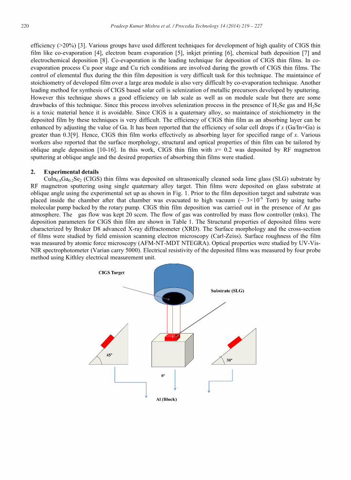
CuIn0.8Ga0.2Se2 (CIGS) thin films was deposited on ultrasonically cleaned soda lime glass (SLG) substrate by RF magnetron sputtering using single quaternary alloy target. Thin films were deposited on glass substrate at oblique angle using the experimental set up as shown in Fig. 1. Prior to the film deposition target and substrate was placed inside the chamber after that chamber was evacuated to high vacuum (~ 3×10⁻⁶ Torr) by using turbo molecular pump backed by the rotary pump. CIGS thin film deposition was carried out in the presence of Ar gas atmosphere. The gas flow was kept 20 sccm. The flow of gas was controlled by mass flow controller (mks). The deposition parameters for CIGS thin film are shown in Table 1. The Structural properties of deposited films were characterized by Bruker D8 advanced X-ray diffractometer (XRD). The Surface morphology and the cross-section of films were studied by field emission scanning electron microscopy (Carl-Zeiss). Surface roughness of the film was measured by atomic force microscopy (AFM-NT-MDT NTEGRA). Optical properties were studied by UV-Vis-NIR spectrophotometer (Varian carry 5000). Electrical resistivity of the deposited films was measured by four probe method using Kithley electrical measurement unit.

221 Pradeep Kumar Mishra et al. / Procedia Technology 14 ( 2014 ) 219 – 227
Fig. 1. Experimental set up for oblique angle deposition of CIGS thin filmsTable 1. Deposition parameters for CIGS thin films
3. Results and discussion
3.1 Structural analysisFig. 2 shows the XRD spectra of CIGS thin films deposited at different oblique angle of deposition. All deposited films possessed (112) preferred orientation at about 26.7° [17]. Other phases along (220/204) and (312) planes were also observed. It was observed that film possesses highest peak intensity along (112) plane for films deposited at 0° (target and substrate parallel to each other). It was also observed that the phases along (220/204) and (312) plane disappeared as oblique angle was increased. The peak intensity along (112) plane was also found to be diminishing with the increase in the oblique angle deposition. The crystallite size of deposited films was calculated using the scherrer’s formula [18]
COS
9.0D (1)
w width at half maxima in radiadegree). It was observed that the film deposited at 0° position possesses larger crystallite size (28 nm) comparison to the films deposited at 60° (16 nm). The reduction in particle size with increase in oblique angle is due to the shadowing effect which occurred during the oblique angle deposition [10, 15].
Fig. 2. XRD spectra of CIGS thin films at different oblique angle configuration
lines/m2 (2)
Target substrate Depositiontime(min)
Working pressure(mTorr)
Target substrate distance(cm)
Substrate temperature(°C)
RF Power (w)
Oblique Angle of deposition
CuIn0.8Ga0.2Se2 SLG 30 5 mTorr 6 500 100 0°, 30°, 45°, 60°

222 Pradeep Kumar Mishra et al. / Procedia Technology 14 ( 2014 ) 219 – 227
It is clear from the Table 2 that less crystal defects were obtained at 0° oblique angle and these defects shows an arising trend with enhancement of oblique angle. It may be due to the decrement in the crystallite size with the increase in oblique angle which in turn reduces the movement of interstitial atoms from grain boundary tocrystallites. As a result, lattice defect in developed films increases [18]. The value of crystallite size and dislocation density of the deposited films is shown in Table 2.
Table 2. Variation of crystallite size and dislocation density of CIGS thin films with oblique angle
Oblique angle(°) Crystallite size (nm) Dislocation density (×1015 lines m-2)
0 28 1.230 22 2.145 18 3.160 16 3.9
3.2 FE-SEM analysis
Fig. 3.FE-SEM images of CIGS thin films deposited at various deposition angle
Fig. 3 highlights the surface morphology of the deposited films at different oblique angle configuration. It was observed that the film deposited at 0° position (target and substrate parallel) exhibits compact and uniform morphology. Compactness in the films surface was found to be slightly reduced at 30° position. However, at higher

223 Pradeep Kumar Mishra et al. / Procedia Technology 14 ( 2014 ) 219 – 227
Fig. 4. FE-SEM cross-section image of CIGS thin films deposited at various oblique angleoblique angle of deposition (i.e. 45° and 60°) slanting morphology was observed. Thickness of the deposited CIGS thin film was calculated using the FE-SEM cross-section image. Fig. 4 shows typical cross-sectional images of CIGS thin film deposited at the different oblique angle. It is clear from the figure that the film deposited at 0° configuration (target substrate parallel to each other) possesses higher thickness (750 nm) compared to the film deposited at higher oblique angle (60°) of deposition (417 nm). The reduction in thickness with oblique angle deposition is probably due to the decrease in area of cross-section of sputtered atom flux and self shielding effect [16]. Also, it was observed that at 60° deposition angle film exhibits somewhat columnar structure.
3.3 AFM analysis
2 dimensional and 3 dimensional AFM images of CIGS thin films are shown in Fig. 5. It was observed from 2D AFM images of CIGS thin films that the film deposited at 0° configuration have large size particles with high compactness in comparison to the films developed at higher oblique angle. The rms value of surface roughness wasdecreasing from 6 nm to 3 nm with increase in oblique angle of sputtering from 0° to 60°. Probably, particle size may be playing role in determining the surface roughness of the films since smaller particle size is associated withsmaller surface roughness of film and vice versa [19]. Hence, films deposited at 60° configuration are smoother than the films deposited at 0°.
Fig. 5. 2D and 3D AFM images of CIGS thin films deposited at different oblique angle
3.4 Optical analysis
Fig. 6 (a) and (b) shows the transmittance and absorbance spectra of CIGS thin films deposited on SLG substrate at different oblique angle of sputtering. It was observed that transparency in the film increases with increase in oblique angle of deposition [15]. The transmittance of film deposited at 0° position was found to be 2.8% while 23% for the films deposited at 60°. The increment in transmittance of CIGS thin films with oblique angle deposition may be due to the reduction in particle size of deposited films. It was also observed from AFM data that film deposited at parallel position i.e. at 0° are somewhat rougher than the films developed at higher oblique angle of sputtering. Since higher surface roughness is always associated with more scattering loss which in turn reduces the transmittance of the films [18]. The reduction in the thickness of the film is also responsible for the

224 Pradeep Kumar Mishra et al. / Procedia Technology 14 ( 2014 ) 219 – 227
increment in transmittance of film with oblique angle deposition [20]. The band gap of deposited film at 0° (target and substrate parallel to each other) and other oblique angle deposition configuration was evaluated using theTauc relation [21]
21
gEhvAhv (3)
tT1log303.2
(4)
Where t = thickness of film and T is the transmittance in %. The band gap of CIGS thin film was estimated from 2 in
oblique angle of sputtering. Variation of surface roughness and band gap of thin film with oblique angle deposition is shown in Table 3.
Table 3. Variation of surface roughness and band gap of thin film with oblique angle deposition
Oblique angle(°)
Surface roughness(nm)
Band gap(eV)
0 6.0 1.1430 5.5 1.1545 4.0 1.1960 3.0 1.33

225 Pradeep Kumar Mishra et al. / Procedia Technology 14 ( 2014 ) 219 – 227
Fig. 6. (a) Transmittance (b) absorbance and (c) band gap of CIGS thin films deposited at different oblique angle3.5 Electrical measurement
Electrical resistivity of deposited film was measured by four probe method and data are listed in Table 4. It was observed that when target and substrate are parallel to each other, the deposited film has low resistivity in comparison to the films deposited at higher oblique angle of sputtering. It may be due to the fact that by increasing the oblique angle of deposition grain growth along a preferred orientation is decreased. Due to this, potential barrier as well as potential barrier height for the charge carriers is increased. As a result, charge carriers have to cross maximum number of grain boundaries during the electrical transport [22-24].
Table 4. Variation of electrical resistivity of CIGS thin films with oblique angle deposition
Oblique angle(°) -cm)
0 0.1330 0.1445 0.1660 0.20

226 Pradeep Kumar Mishra et al. / Procedia Technology 14 ( 2014 ) 219 – 227
Conclusion CIGS thin films were deposited successfully on SLG substrate at different oblique angle of sputtering. It was observed that thin film deposited at 0° position (target substrate parallel to each other) is larger in crystallite size, with low dislocation density. Film was found to be high absorber in visible region. Film also possessed high compactness without any microcracks and pits. Compactness was showing declining trend at higher oblique angle configuration. However, columnar grain structure was observed at 45° and 60° position. Transmittance of deposited film at higher oblique angle deposition was increased due to reduction in thickness as well as roughness of the film. The electrical resistivity of the deposited CIGS thin film was increasing with the increase in the oblique angle deposition due to reduction in crystallite size of CIGS thin films.
Acknowledgment One of the authors Pradeep K. Mishra is thankful to DST, New Delhi for financial support towards this research work.
References[1] C. Xu, H. Zhang, J. Parry, S. Perera, G. Long, H. Zhang. A single source three stage evaporation approach to CIGS absorber layer for
thin film solar cells. Sol. Energy Mater. Sol. Cells 2013;117:357-362.[2] Y.H. Jo, B.C. Mohanty, Y.S. Cho. Enhanced electrical properties of pulsed laser deposited CuIn0.7Ga0.3Se2 thin films via processing
control. Sol. Energy 2010;84:2213-2218.[3] M. Nerat. Copper indium gallium selenide (CIGS) solar cells with localized back contact for achieving high performance. Sol. Energy
Mater. Sol. Cells 2012;104:152-158.[4] L. Zhang, F.F. Liu, F.Y. Li, Q. He, B.Z. Li, C.J. Li. Structural, optical and electrical properties of low temperature deposition Cu(InxGa1-
x)Se2. Sol. Energy Mater. Sol. Cells 2012;99:356-361.[5] Z.H. Li, E.S. Cho, S.J. Kown. Properties of the Cu(In,Ga)Se2 absorbers deposited by electron beam evaporation method for solar cells.
Curr. Appl Phys. 2011;11:28-33.[6] W. Wang, Y.W. Su, C.H. Chang. Inkjet printed chalcopyrite CuIn(1-x)GaxSe2 thin film solar cells. Sol. Energy Mater. Sol. Cells
2011;95:2616-2620.[7] M. Chandramohan, S. Velumani, T. Venkatachalam. Experimental and theoretical investigations of structural and optical properties of
CIGS thin films. Mater. Sci. Eng., B 2010;174:205-208.[8] V.S. Saji, I.C. Choi, C.W. Lee. Progress in electrodeposited absorber layer for CuIn(1-x)GaxSe2 (CIGS) solar cells. Sol. Energy 2011;
85:2666-2678.[9] S.H. Wei, S.B. Zhang, A. Zunger. Effect of Ga addition to CuInSe2 on its electronic, structural and defect properties. Appl. Phys. Lett.
1998;72:3199-3201.[10] X. Xiao, G. Dong, J. Shao, H. He, Z. Fan. Optical and electrical properties of SnO2: Sb thin films deposited by oblique angle deposition.
Appl. Surf. Sci. 2010;256:1636-1640.[11] D. Vick, L.J. Friedrich, S.K. Dew, M.J. Brett, K. Robbie, M. Seto, T. Smy. Self-shadowing and surface diffusion effects in obliquely
deposited thin films. Thin Solid Films 1999;339:88-94.[12] D. J. Poxson, F. W. Mont, M. F. Schubert, J. K. Kim, E. F. Schubert. Quantification of porosity and deposition rate of nanoporous films
grown by oblique-angle deposition. Appl. Phys. Lett. 2008;93:101914(1-3).[13] I. Cerven, T. Lacko, 1. Novotny, V. Tvarozek, M. Harvanka. Texture of obliquely sputtered ZnO thin films. J. Cryst. Growth
1993;131:546-550.[14] M. Singh, K.C. Bhahada, Y.K. Vijay. Variation of optical band gap in obliquely deposited Selenium thin films. Indian J. Pure Appl.
Phys. 2005;43:129-13.[15] L. Abelmann, C. Lodder. Oblique evaporation and surface diffusion. Thin Solid Films 1997;305:1-21.[16] R.K. Jain, Y.K. Gautam, V. Dave, A.K. Chawla, R. Chandra. A study on structural, optical and hydrophobic properties of oblique angle
sputter deposited HfO2 films. Appl. Surf. Sci. 2013;283:332-338.[17] M. Venkatachalam, M.D. Kannan, S. Jayakumar, R. Balasundaraprabhu, A.K. Nandakumar, N. Muthukumarasamy. CuInxGa1-xSe2 thin
films prepared by electron beam evaporation. Sol. Energy Mater. Sol. Cells 2008;92:571-575.[18] P. Matheswaran, B. Gokul, K.M. Abhirami, R. Sathyamoorhy. Thickness dependent structural, optical properties of In/Te bilayer thin
films. Mater. Sci. Semicond. Process. 2012;15:486-491.[19] V. Chawla, R. Jayaganthan, A.K. Chawla, R. Chandra. Microstructural characterization of magnetron sputtered Ti films on glass
substrate. J. Mater. Process. Technol. 2009;209:3444-3451.[20] Y. Sato, K. Yanagisawa, N. Oka, S. Nakamura, Y. Shigesato. Sputter deposition of Al doped ZnO films with various incident angles. J.
Vac. Sci. Technol. 2009;27(5):1166-1171.[21] Z. Yu, Y. Yan, Y. Zhang, C. Yan, L. Liu, Y. Zhang, Y. Zhao. Significant effect of substrate temperature on the phase structure, optical
and electrical properties of RF sputtered CIGS films. Appl. Surf. Sci. 2013;264:197-201.[22] G. Gordillo, F. Mesa, C. Calderon. Electrical and morphological properties of low resistivity Mo thin films prepared by magnetron
sputtering. Braz. J. Phys. 2006;36:982-985.

227 Pradeep Kumar Mishra et al. / Procedia Technology 14 ( 2014 ) 219 – 227
[23] N. M. Shah, J. R. Ray, V. A. Kheraj, M. S. Desai, C. J. Panchal, B. Rehani. Structural, optical and electrical properties of flash-evaporated copper indium diselenide thin films. J Mater Sci 2009;44:316–322.
[24] A. Han, Y. Zhang, W. Song, B. Li, W. Liu, Y. Sun. Structure, morphology and properties of thinned Cu(In, Ga)Se2 films and solar cells.Semicond. Sci. Technol. 2012; 27:035022 (8pp).
Copyright © 2022 FDOKUMEN