Fabrication and characterization of low loss rib chalcogenide waveguides made by dry etching
Upload
khangminh22Category
view
2download
0
ACTAUNIVERSITATIS
UPSALIENSISUPPSALA
2017
Digital Comprehensive Summaries of Uppsala Dissertationsfrom the Faculty of Science and Technology 1564
Sputtering-based processes for thinfilm chalcogenide solar cells onsteel substrates
PATRICE BRAS
ISSN 1651-6214ISBN 978-91-513-0078-8urn:nbn:se:uu:diva-329778

Dissertation presented at Uppsala University to be publicly examined in Polhemssalen,Ångström laboratory, Lägerhyddsvägen 1, Uppsala, Thursday, 9 November 2017 at 09:15 forthe degree of Doctor of Philosophy. The examination will be conducted in English. Facultyexaminer: PhD Veronica Bernudez (Solar Frontier K.K.).
AbstractBras, P. 2017. Sputtering-based processes for thin film chalcogenide solar cells on steelsubstrates. Digital Comprehensive Summaries of Uppsala Dissertations from the Facultyof Science and Technology 1564. 107 pp. Uppsala: Acta Universitatis Upsaliensis.ISBN 978-91-513-0078-8.
Thin film chalcogenide solar cells are promising photovoltaic technologies. Cu(In,Ga)Se2
(CIGS)-based devices are already produced at industrial scale and record laboratory efficiencysurpasses 22 %. Cu2ZnSn(S,Se)4 (CZTS) is an alternative material that is based on earth-abundant elements. CZTS device efficiency above 12 % has been obtained, indicating a highpotential for improvement.
In this thesis, in-line vacuum, sputtering-based processes for the fabrication of completethin film chalcogenide solar cells on stainless steel substrates are studied. CIGS absorbers aredeposited in a one-step high-temperature process using compound targets. CZTS precursorsare first deposited by room temperature sputtering and absorbers are then formed by hightemperature crystallization in a controlled atmosphere. In both cases, strategies for absorberlayer improvement are identified and implemented.
The impact of CZTS annealing temperature is studied and it is observed that the absorbergrain size increases with annealing temperature up to 550 °C. While performance also improvesfrom 420 to 510 °C, a drop in all solar cell parameters is observed for higher temperature. Thisloss is caused by blisters forming in the absorber during annealing. Blister formation is foundto originate from gas entrapment during precursor sputtering. Increase in substrate temperatureor sputtering pressure leads to drastic reduction of gas entrapment and hence alleviate blisterformation resulting in improved solar cell parameters, including efficiency.
An investigation of bandgap grading in industrial CIGS devices is conducted through one-dimensional simulations and experimental verification. It is found that a single gradient in theconduction band edge extending throughout the absorber combined with a steeper back-gradingleads to improved solar cell performance, mainly due to charge carrier collection enhancement.
The uniformity of both CIGS and CZTS 6-inch solar cells is assessed. For CZTS, the deviceuniformity is mainly limited by the in-line annealing process. Uneven heat and gas distributionresulting from natural convection phenomenon leads to significant lateral variation in materialproperties and device performance. CIGS solar cell uniformity is studied through laterally-resolved material and device characterization combined with SPICE network modeling. Theabsorber material is found to be laterally homogeneous. Moderate variations observed at thedevice level are discussed in the context of large area sample characterization.
Power conversion efficiency values above 15 % for 225 cm2 CIGS cells and up to 5.1 % for1 cm2 CZTS solar cells are obtained.
Keywords: CIGS, CZTS, solar cell, photovoltaics, thin film, sputtering, annealing, galliumgrading, blister, uniformity, stainless steel
Patrice Bras, Department of Engineering Sciences, Solid State Electronics, Box 534, UppsalaUniversity, SE-75121 Uppsala, Sweden.
© Patrice Bras 2017
ISSN 1651-6214ISBN 978-91-513-0078-8urn:nbn:se:uu:diva-329778 (http://urn.kb.se/resolve?urn=urn:nbn:se:uu:diva-329778)

Dedicated to my family


List of papers
This thesis is based on the following papers, which are referred to in the textby their Roman numerals.
I P. Bras, J. Sterner, C. Platzer-Björkman, “Influence of hydrogen sulfideannealing on copper–zinc–tin–sulfide solar cells sputtered from aquaternary compound target”, Thin Solid Films, 582, 2015, pp.233-238. DOI:http://dx.doi.org/10.1016/j.tsf.2014.11.004
II P. Bras, J. Sterner, C. Platzer-Björkman, “Investigation of blisterformation in sputtered Cu2ZnSnS4 absorbers for thin film solar cells”,Journal of Vacuum Science & Technology A, 33, 2015, 061201. DOI:http://dx.doi.org/10.1116/1.4926754
III P. Bras, C. Frisk, A. Tempez, E. Niemi, C. Platzer-Björkman,“Ga-grading and Solar Cell Capacitance Simulation of an industrialCu(In,Ga)Se2 solar cell produced by an in-line vacuum, all-sputteringprocess”, Thin Solid Films, 582, 2017, pp. 367-374. DOI:http://dx.doi.org/10.1016/j.tsf.2017.06.031
IV P. Bras, L. Mauvy, J. Sterner, C. Platzer-Björkman, ”Uniformityassessment of a 6-inch copper-zinc-tin-sulfide solar cell sputtered froma quaternary compound target”, Proceedings of the 42nd PhotovoltaicSpecialist Conference (PVSC), New Orleans, LA, USA, 2015, pp. 1-4.DOI: http://dx.doi.org/10.1109/PVSC.2015.7356103
V P. Bras, A. Davydova, C. Platzer-Björkman, ”SPICE network modelingof a 6-inch Cu(In,Ga)Se2 solar cell”, in manuscript.
Reprints were made with permission from the publishers.


Personal contribution to the papers
I Contribution to the definition of the research project, sample fabrication,sample characterization, data analysis and paper writing with input fromco-authors.
II Contribution to the definition of the research project, design of experi-ments, sample processing, major part of the characterization, data anal-ysis and paper writing with input from co-authors.
III Definition of the research project and scope of the investigation, sam-ple fabrication, major part of the characterization, data analysis, SCAPSmodel build-up, simulations and paperwriting with input from co-authors.
IV Definition of the research project and scope of the investigation, part ofthe sample fabrication, part of the characterization, data analysis, simu-lations and paper writing with input from co-authors.
V Definition of the research project and scope of the investigation, samplefabrication, major part of the characterization, data analysis, SPICE sim-ulations and paper writing with input from co-authors.

Abbreviations and acronyms
CIGS Cu(In,Ga)Se2CZTS Cu2ZnSn(S,Se)4PV PhotovoltaicsBIPV Building-integrated photovoltaicsPIPV Product-integrated photovoltaicsSCAPS Solar cell capacitance simulatorSPICE Simulation program with integrated circuit emphasisSRH Shockley-Read-HallCBD Chemical bath depositionTCO Transparent conductive oxideITO In2O3:SnO2CIS CuInSe2CGS CuGaSe2NREL National renewable energy laboratoryPVD Physical vapor depositionGGI Ga/(Ga+In)DC Direct currentRF Radio-frequencyQR Quick responseOBO One-by-oneSEM Scanning electron microscopeEDX or EDS Energy-dispersive x-ray spectroscopyXRF X-ray fluorescenceXRD X-ray diffractionGIXRD Grazing incidence x-ray diffractionCTS Cu2SnS3PP-TOFMSTM Plasma profiling time of flight mass spectrometryIV Current-voltageJV Current density-voltageQE Quantum efficiencyEQE External quantum efficiencyIQE Internal quantum efficiencyAC Alternating currentMoNa Mo:Na2MoO4CV Capacitance-voltage
Contents
Part I: Introduction . . . . . . . . . . . . . . . . . . . . . . . . . . . . . . . . . . . . . . . . . . . . . . . . . . . . . . . . . . . . . . . . . . . . . . . . . . . . . . . . . . . . . . . . . . . 11
1 Renewables in a shifting global energy system . . . . . . . . . . . . . . . . . . . . . . . . . . . . . . . . . . . . . . . 13
2 Solar energy and photovoltaics . . . . . . . . . . . . . . . . . . . . . . . . . . . . . . . . . . . . . . . . . . . . . . . . . . . . . . . . . . . . . . . . . 14
3 Thin film photovoltaics . . . . . . . . . . . . . . . . . . . . . . . . . . . . . . . . . . . . . . . . . . . . . . . . . . . . . . . . . . . . . . . . . . . . . . . . . . . . . 15
Motivation and aim . . . . . . . . . . . . . . . . . . . . . . . . . . . . . . . . . . . . . . . . . . . . . . . . . . . . . . . . . . . . . . . . . . . . . . . . . . . . . . . . . . . 16
Part II: Theory . . . . . . . . . . . . . . . . . . . . . . . . . . . . . . . . . . . . . . . . . . . . . . . . . . . . . . . . . . . . . . . . . . . . . . . . . . . . . . . . . . . . . . . . . . . . . . . . . . 19
4 Thin film chalcogenide solar cells . . . . . . . . . . . . . . . . . . . . . . . . . . . . . . . . . . . . . . . . . . . . . . . . . . . . . . . . . . . . 214.1 Solar cell operating principle . . . . . . . . . . . . . . . . . . . . . . . . . . . . . . . . . . . . . . . . . . . . . . . . . . . . . . . . 21
4.1.1 Semiconductor properties . . . . . . . . . . . . . . . . . . . . . . . . . . . . . . . . . . . . . . . . . . . . . . . 214.1.2 Requirements for a solar cell device . . . . . . . . . . . . . . . . . . . . . . . . . . . . . . 264.1.3 PN junction . . . . . . . . . . . . . . . . . . . . . . . . . . . . . . . . . . . . . . . . . . . . . . . . . . . . . . . . . . . . . . . . . . . . . . 284.1.4 Real solar cells . . . . . . . . . . . . . . . . . . . . . . . . . . . . . . . . . . . . . . . . . . . . . . . . . . . . . . . . . . . . . . . . . 31
4.2 Thin-film heterojunction solar cells . . . . . . . . . . . . . . . . . . . . . . . . . . . . . . . . . . . . . . . . . . . . . . 334.3 Cu(In,Ga)Se2 solar cells . . . . . . . . . . . . . . . . . . . . . . . . . . . . . . . . . . . . . . . . . . . . . . . . . . . . . . . . . . . . . . . . 34
4.3.1 Material properties . . . . . . . . . . . . . . . . . . . . . . . . . . . . . . . . . . . . . . . . . . . . . . . . . . . . . . . . . . 344.3.2 Bandgap grading . . . . . . . . . . . . . . . . . . . . . . . . . . . . . . . . . . . . . . . . . . . . . . . . . . . . . . . . . . . . . . 36
4.4 Cu2ZnSn(S,Se)4 solar cells . . . . . . . . . . . . . . . . . . . . . . . . . . . . . . . . . . . . . . . . . . . . . . . . . . . . . . . . . . . . 384.4.1 Material properties . . . . . . . . . . . . . . . . . . . . . . . . . . . . . . . . . . . . . . . . . . . . . . . . . . . . . . . . . . 384.4.2 Thermodynamic stability and consequences . . . . . . . . . . . . . . . . . 39
5 Thin film deposition by sputtering . . . . . . . . . . . . . . . . . . . . . . . . . . . . . . . . . . . . . . . . . . . . . . . . . . . . . . . . . . . 415.1 Principles and parameters . . . . . . . . . . . . . . . . . . . . . . . . . . . . . . . . . . . . . . . . . . . . . . . . . . . . . . . . . . . . . . 41
5.1.1 Principles of sputtering . . . . . . . . . . . . . . . . . . . . . . . . . . . . . . . . . . . . . . . . . . . . . . . . . . . 415.1.2 Pulsed DC magnetron sputtering . . . . . . . . . . . . . . . . . . . . . . . . . . . . . . . . . . . . 43
5.2 Sputtering from a compound target . . . . . . . . . . . . . . . . . . . . . . . . . . . . . . . . . . . . . . . . . . . . . . 445.2.1 Compound target and implications during sputtering
process . . . . . . . . . . . . . . . . . . . . . . . . . . . . . . . . . . . . . . . . . . . . . . . . . . . . . . . . . . . . . . . . . . . . . . . . . . . . . . 455.2.2 CIGS and CZTS sputtered from a compound target . . . . . 45
5.3 Gas entrapment . . . . . . . . . . . . . . . . . . . . . . . . . . . . . . . . . . . . . . . . . . . . . . . . . . . . . . . . . . . . . . . . . . . . . . . . . . . . . . . 47
Part III: Process and characterization . . . . . . . . . . . . . . . . . . . . . . . . . . . . . . . . . . . . . . . . . . . . . . . . . . . . . . . . . . . . . 49
6 Process description . . . . . . . . . . . . . . . . . . . . . . . . . . . . . . . . . . . . . . . . . . . . . . . . . . . . . . . . . . . . . . . . . . . . . . . . . . . . . . . . . . . . 51

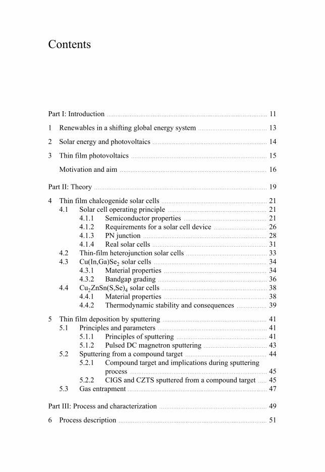
6.1 General process flow: From stainless steel substrates tofinalized devices . . . . . . . . . . . . . . . . . . . . . . . . . . . . . . . . . . . . . . . . . . . . . . . . . . . . . . . . . . . . . . . . . . . . . . . . . . . . . 51
6.2 CIGS: the DUO process . . . . . . . . . . . . . . . . . . . . . . . . . . . . . . . . . . . . . . . . . . . . . . . . . . . . . . . . . . . . . . . . 526.3 CZTS sputtering and annealing . . . . . . . . . . . . . . . . . . . . . . . . . . . . . . . . . . . . . . . . . . . . . . . . . . . . . 55
7 Characterization methods and simulations . . . . . . . . . . . . . . . . . . . . . . . . . . . . . . . . . . . . . . . . . . . . . . 567.1 Material and device characterization . . . . . . . . . . . . . . . . . . . . . . . . . . . . . . . . . . . . . . . . . . . . 56
7.1.1 Scanning electron microscopy (SEM) and energydispersive x-ray spectroscopy (EDX) . . . . . . . . . . . . . . . . . . . . . . . . . . . . 56
7.1.2 X-ray fluorescence (XRF) . . . . . . . . . . . . . . . . . . . . . . . . . . . . . . . . . . . . . . . . . . . . . . . 577.1.3 X-ray diffraction (XRD) . . . . . . . . . . . . . . . . . . . . . . . . . . . . . . . . . . . . . . . . . . . . . . . . . 587.1.4 Raman spectroscopy . . . . . . . . . . . . . . . . . . . . . . . . . . . . . . . . . . . . . . . . . . . . . . . . . . . . . . . . 597.1.5 Plasma profiling time of flight mass spectrometry
(PP-TOFMSTM) . . . . . . . . . . . . . . . . . . . . . . . . . . . . . . . . . . . . . . . . . . . . . . . . . . . . . . . . . . . . . . . 597.1.6 Current-voltage measurements . . . . . . . . . . . . . . . . . . . . . . . . . . . . . . . . . . . . . . . 607.1.7 Quantum efficiency . . . . . . . . . . . . . . . . . . . . . . . . . . . . . . . . . . . . . . . . . . . . . . . . . . . . . . . . . 60
7.2 Simulations . . . . . . . . . . . . . . . . . . . . . . . . . . . . . . . . . . . . . . . . . . . . . . . . . . . . . . . . . . . . . . . . . . . . . . . . . . . . . . . . . . . . . 627.2.1 SCAPS . . . . . . . . . . . . . . . . . . . . . . . . . . . . . . . . . . . . . . . . . . . . . . . . . . . . . . . . . . . . . . . . . . . . . . . . . . . . . . 637.2.2 SPICE . . . . . . . . . . . . . . . . . . . . . . . . . . . . . . . . . . . . . . . . . . . . . . . . . . . . . . . . . . . . . . . . . . . . . . . . . . . . . . . 63
Part IV: Results and discussion . . . . . . . . . . . . . . . . . . . . . . . . . . . . . . . . . . . . . . . . . . . . . . . . . . . . . . . . . . . . . . . . . . . . . . . 67
8 Improvement of thin film solar cell absorber layers and uniformity of6-inch devices . . . . . . . . . . . . . . . . . . . . . . . . . . . . . . . . . . . . . . . . . . . . . . . . . . . . . . . . . . . . . . . . . . . . . . . . . . . . . . . . . . . . . . . . . . . . 698.1 Annealing CZTS absorbers (Paper I and II) . . . . . . . . . . . . . . . . . . . . . . . . . . . . . . . . . 698.2 Bandgap grading for industrial CIGS solar cells (Paper III) . . . . . . . 748.3 Uniformity of 6-inch chalcogenide solar cells (Paper IV and V) 77
8.3.1 Laterally-resolved characterization and simulation ofCIGS absorbers and full solar cells . . . . . . . . . . . . . . . . . . . . . . . . . . . . . . . . 77
8.3.2 Sputtering and annealing process uniformity for 6-inchCZTS device fabrication . . . . . . . . . . . . . . . . . . . . . . . . . . . . . . . . . . . . . . . . . . . . . . . . . 79
9 Concluding remarks . . . . . . . . . . . . . . . . . . . . . . . . . . . . . . . . . . . . . . . . . . . . . . . . . . . . . . . . . . . . . . . . . . . . . . . . . . . . . . . . . . 81
10 Future work . . . . . . . . . . . . . . . . . . . . . . . . . . . . . . . . . . . . . . . . . . . . . . . . . . . . . . . . . . . . . . . . . . . . . . . . . . . . . . . . . . . . . . . . . . . . . . . . 83
Sammanfattning på svenska . . . . . . . . . . . . . . . . . . . . . . . . . . . . . . . . . . . . . . . . . . . . . . . . . . . . . . . . . . . . . . . . . . . . . . 85
Résumé en français . . . . . . . . . . . . . . . . . . . . . . . . . . . . . . . . . . . . . . . . . . . . . . . . . . . . . . . . . . . . . . . . . . . . . . . . . . . . . . . . . . . . 88
Acknowledgements . . . . . . . . . . . . . . . . . . . . . . . . . . . . . . . . . . . . . . . . . . . . . . . . . . . . . . . . . . . . . . . . . . . . . . . . . . . . . . . . . . . 92
References . . . . . . . . . . . . . . . . . . . . . . . . . . . . . . . . . . . . . . . . . . . . . . . . . . . . . . . . . . . . . . . . . . . . . . . . . . . . . . . . . . . . . . . . . . . . . . . . . . . . . . . . 94

Part I:IntroductionGlobal energy landscape and solar energy


1. Renewables in a shifting global energysystem
The industrial revolution and all the related technological progress broughttremendous improvement in quality of life to humankind. One significant andadverse consequence, however, is the ever increasing energy consumption thatcharacterizes modern world. Up to the end of the 20th century, mostly fossilresources such as coal, oil or gas have been used to satisfy the needs. Fossil fu-els are finite by definition and their utilization ineluctably leads to greenhousegas emissions which have terrible consequences on the environment and publichealth [1].
The need for a paradigm shift in our energy supply has been frequentlypointed out (see for instance [2]) and evidence of a growing awareness frompeople, the private and the public sector, is observed everyday despite themagnitude of the challenge ahead. Politically, the Paris climate agreement of2015 [3] sets the basis for a global transition towards a more environmentally-friendly energy model. On the industrial side, multiple large scale power plants(with capacities of several hundred MWp and up to the GWp level), basedon renewable sources and exhibiting competitive energy prices, have recentlybeen inaugurated and numerous other projects are soon to be realized [4].Technologically speaking, scientists and engineers have found effective waysto harness energy from a variety of renewable sources available in Nature.The gravitational potential energy of water is exploited in various types ofhydropower plants. The kinetic energy carried by winds is transformed intoelectricity by wind turbines. The electromagnetic energy radiated by the suncan be harnessed to produce heat, electricity or even synthetic fuels. Numer-ous exploitation strategies of other renewable energy sources are also beingdeveloped. Combining them all, a share of 18% of the total primary energysupply has been reached in 2014 [5]. Focusing on electricity, this proportionincreases above 23% [5]. Although these numbers may appear low, the factthat the share of renewable power generation has grown at an average annualrate of 6% since 2009 combined with a recent drop in the cost of wind turbinesand solar panels (30% and 80% respectively compared to 2009) is source ofoptimism for the coming decades [5]. Nevertheless, a lot remains to be doneif we are to achieve the ambitious but necessary goals of the Paris agreement.
13

2. Solar energy and photovoltaics
The average incident solar irradiance on the surface of the earth is close to 160W.m-2 [6]. The world total primary energy supply in 2014 was estimated to bearound 160 000 TWh (13699 Mtoe) [7]. Considering the surface area of ourplanet, it is relatively easy to conclude that it receives from the sun, in just acouple of hours, the equivalent of the energy consumed by all human activityduring a year. Of course, it is not practically possible to harness all this energybut it gives a representative idea of the potential of solar power. Solar energycan be converted into heat using solar thermal technologies or directly intoelectricity via the photovoltaic (PV) effect.
The photovoltaic effect was discovered by the French physicist EdmondBecquerel in 1839 [8]. After more than a century spent on improving the un-derstanding of the underlying physics and developing experimental proofs, thefirst silicon solar cell appeared in Bell Labs in 1954 with a power conversionefficiency of 6% [9]. During the second half of the 20th century, intense re-search activities on PV cells have led to technology upscaling accompaniedby constant improvement of solar cell performance. Mainly used in spatialapplications at first, solar cells and solar panels gradually expanded towardsother types of applications. Different solar programs funded by public subsi-dies in Europe, Japan and the USA during the 1990s and 2000s associated withindustrial development have led to the generalization of PV adoption and thecreation of numerous power plants based on solar panels all over the world.The achievement of levelized cost of electricity equivalent to or lower thanconventional power plants in several recent PV projects constitutes an impor-tant milestone towards a much wider penetration of solar energy in today’senergy landscape [10].
14

3. Thin film photovoltaics
The dominant PV technologies on the market nowadays are based on silicon.Building on decades of research in microelectronics which have led to the syn-thesis of extremely pure and high quality material at a relatively low cost, sili-con is a natural candidate for efficient solar cell manufacturing. Power conver-sion efficiency for record Si solar cells is above 26 %[11] while it ranges from15 to more than 20 % for commercial modules, depending on the technology.However, silicon is not the perfect candidate for all PV applications. First ofall, standard crystalline Si cells need to be rather thick (several tens of micronsat least) in order to absorb a significant part of sunlight and the correspondingcells are fragile leading to bulky and heavy, glass-encapsulated solar panels.Thin-film technologies are based on different types of semiconductor materialused as light absorbers. They typically exhibit a higher absorption coefficientthan crystalline silicon which means that a few micron-thick layer is sufficientto absorb sunlight effectively. Historically, amorphous silicon has played animportant role in the field of thin film solar cells although it is heavily declin-ing nowadays due to relatively low efficiency and light-induced degradation.Copper indium gallium selenide (Cu(In,Ga)Se2, CIGS) and cadmium telluride(CdTe)-based solar cells are the most promising thin film technologies thathave already reached the commercial stage. At the research and developmentscale, solar submodules above 18% for these two technologies have been re-ported [12] while commercially available modules exhibit total area efficien-cies in the range 14-16% depending on the manufacturer and the technology[13, 14].
Concerns about the toxicity of Cd as well as the potential scarcity of Teand In have triggered intense research effort to find more earth-abundant andnon-toxic thin film absorber materials for solar cells. Cu2ZnSn(S,Se)4 (CZTS)has been identified as a potential alternative that matches well the previouslymentioned criteria. Record solar cell efficiency for this material is 12.6% atthe research scale denoting a high improvement potential [15].
15

Motivation and aim
Our current electricity supply is mainly based on centralized generation in largepower plants and wide-scale distribution through the power grid. As previ-ously mentioned, photovoltaics is compatible with this approach and largescale PV plants allow to reach the lowest electricity price due to scale ef-fects. However, one important characteristic of sunlight is its distributed naturemeaning that it is available almost anywhere on Earth as long as sun is shin-ing. As a consequence, electricity generation can also take place much closer towhere it is consumed, limiting transportation-related losses, additional costs,guaranteeing partial or complete energy autonomy to buildings and devices,and increasing resilience in case of power grid failure. In this context, theconcept of building integrated photovoltaics (BIPV) is now considered as animportant component of the photovoltaic energy production of the future.
BIPV is the combination of a photovoltaic cell or module and a construc-tion material to obtain a product that exhibits electricity generation capabilitytogether with some building-related function. One of the most common exam-ples are photovoltaic panels integrated in rooftops or facades. In this case, theelectricity generation function is coupled to the protection and waterproofnessexpected from the building component.
Product integrated photovoltaics or PIPV is the extension of this conceptto any kind of products with an emphasis on new digital technologies rangingfrom portable consumer electronics (tablets, portable chargers) to network ofautonomous sensors (internet of things).
Thin film PV technologies are particularly adapted to applications in thefields of BIPV and PIPV. CIGS, for instance, can be deposited on flexibleand light-weight substrates using mature thin-film deposition techniques suchas sputtering or evaporation. The integration of such cell into, for instance,building material, is facilitated compared to crystalline silicon due to enhancedmodularity in terms of shape, size, mechanical properties and device parame-ters.
Midsummer AB has developed a process exclusively based on sputtering forthe fabrication of CIGS solar cells on thin stainless steel substrates. Optimiza-tion of the process for CIGS solar cell fabrication to reach higher performancelevel is critical in an industrial context to guarantee further penetration of thetechnology into the market. On the other hand, exploring related promisingalternative technologies based on more earth-abundant materials appears to bealso necessary for wider spread of thin film PV technologies in a longer termfuture.
16

This thesis, conducted in collaboration between Midsummer AB and Up-psala University, focuses on the optimization of absorber layer synthesis forapplication in thin film solar cells. The main efficiency bottlenecks relatedto CIGS and CZTS absorber formation within the framework of an industrialprocess are identified and studied.
For CIGS solar cells, the one step sputtering of the absorber layer leads tolower minority carrier lifetime compared to samples typically obtained in re-search context. Additionally, the accessible thickness range is limited to aboutone micrometer to guarantee low cycle time and high throughput in produc-tion. The implications of these constraints on optimal bandgap grading areinvestigated both experimentally, through the use of CIGS compound targetswith different In/Ga content, and by device simulations using SCAPS.
Due to thermodynamic instability of CZTS above 500 °C in vacuum, onestep deposition of absorbers at high temperature is particularly challenging. Aprocess for CZTS solar cells on steel substrates based on room temperaturesputtering followed by annealing in a controlled atmosphere and compatiblewith Midsummer’s technology is also proposed and studied. Fine tuning oftemperature and sulfur partial pressure during the annealing sequence are pre-ponderant parameters for obtaining CZTS absorbers with appropriate optoelec-tronic properties. A particular attention is given to the effect of temperatureduring 15 minute-long, in-line vacuum annealing process. While performanceincreases for intermediate temperatures, a drop in all solar cell parameters isobserved for higher temperature. The reason for this performance loss is stud-ied in detail and routes for avoiding the problem are suggested.
Uniformity of all layers in thin film solar cells is one of the most importantcharacteristics sought after when working on large area industrial devices. Thegeometry of solar cells produced at Midsummer resembles silicon cells butpotentially exhibit non-homogeneity inherent to large area thin film deposition.For CIGS, experimental assessment of lateral non-uniformity is compared to a2D network model based on SPICE, developed to relate local device propertiesto the performance of the full size solar cell. 6-inch CZTS device uniformityis found to be mainly dictated by the annealing process, performed verticallydue to equipment design. The effect of the annealing chamber configurationon lateral non-uniformity of CZTS is studied.
17


Part II:TheoryThin film solar cells based on Cu(In,Ga)Se2 and Cu2ZnSn(S,Se)4


4. Thin film chalcogenide solar cells
CuInSe2 (CIS) and later Cu(In,Ga)Se2 (CIGS) solar cells have been investi-gated for more than 40 years [16]. Both incremental and more disruptive re-search at the material, process and device structure levels have allowed effi-ciency improvements over the years to reach a laboratory scale record value of22.6% in 2016 [17]. CZTS development is more recent [18] and greatly ben-efited from research findings related to CIGS technology. However, intrinsicthermodynamic instability of CZTS at high temperature and more complex de-fect chemistry compared to CIGS are two important differences that contributeto the performance gap between these two technologies. The purpose of thischapter is, first, to describe the general operating principle of a solar cell andto briefly introduce its main parameters. The material properties of both CIGSand CZTS are then explored. In each case, a specific topic related to solar cellabsorber optoelectronic properties optimization is examined, namely bandgapgrading for CIGS and high temperature annealing for CZTS.
4.1 Solar cell operating principleThis section starts with a short review of important semiconductor properties.Then, the requirements for designing an efficient solar cell are discussed. Sub-sequently, a summary of the physics of the main component of solid state solarcells, the PN junction, is given. Finally, the solar cell performance parametersare described.
4.1.1 Semiconductor propertiesCharge carrier concentration in a semiconductorSemiconductors and insulators are materials exhibiting a special energy bandstructure where a valence and a conduction band are separated by a so-calledenergy gap, 𝐸𝑔, where no allowed energy states are present. They differ by themagnitude of the bandgap where the distinction is mainly a matter of conven-tion. 𝐸𝑔 values for semiconductors are generally below 5 eV. Larger bandgapmaterials are most of the time considered as insulators.
Due to thermal or external excitation such as light shining on the material,some electrons from the valence band can be transferred to the conduction bandleaving behind a positive quasi-particle called hole. The carrier concentration
21

in the valence and the conduction band of a semiconductor can be obtainedby first multiplying the density of available states in each of the bands by thecorresponding occupation function given by the Fermi-Dirac distribution andby integrating the result over all accessible energy levels. The so-called Fermilevel of the semiconductor is then defined as the energy level that has a 50%probability of being occupied. Using the Boltzmann approximation, the den-sity of electrons in the conduction band 𝑛 and holes in the valence band 𝑝 canbe calculated with equations (4.1) and (4.2).
𝑛 = 𝑁𝐶𝑒𝑥𝑝 (𝐸𝐹 − 𝐸𝐶𝑘𝐵𝑇 ) (4.1)
𝑝 = 𝑁𝑉 𝑒𝑥𝑝 (𝐸𝑉 − 𝐸𝐹𝑘𝐵𝑇 ) (4.2)
𝑁𝑉 and 𝑁𝐶 are the effective density of states in the valence and conductionband which depend on the effective mass of holes and electrons respectively.Further discussion on these parameters is available in, for instance, [19]. 𝐸𝑉is the energy level corresponding to the to top of the valence band and 𝐸𝐶corresponds to the bottom of the conduction band. 𝐸𝐹 represents the Fermilevel, 𝑘𝐵 is Boltzmann constant and T is the temperature.
In thermal equilibrium condition, and for a non-doped or intrinsic semicon-ductor, some free electrons and holes are thermally generated. Their concen-tration corresponds to the intrinsic concentration 𝑛𝑖 which depends on tem-perature. Generalizing to all semiconductors (undoped and doped) at thermalequilibrium, the square of the intrinsic carrier concentration is equal to the con-centration of electrons in the conduction band multiplied by the concentrationof holes in the valence band as shown in eq. (4.3).
𝑛𝑝 = 𝑛2𝑖 = 𝑁𝐶𝑁𝑉 𝑒𝑥𝑝 (𝐸𝑉 − 𝐸𝐶
𝑘𝐵𝑇 ) = 𝑁𝐶𝑁𝑉 𝑒𝑥𝑝 (− 𝐸𝑔𝑘𝐵𝑇 ) (4.3)
Doping in a semiconductorOne important characteristic of a semiconductor is that its free charge carrierdensity can be modified by doping. Doping can be intentional, as for instancein silicon solar cells. In this case, so-called donor or acceptor atoms are delib-erately introduced into the Si lattice. Donor atoms such as phosphorus exhibitan additional valence electron compared to silicon. This electron will not takepart in the formation of a covalent bond and it will act as a free electron whenthe dopant atom is ionized. In terms of energy band diagram, the inclusionof such impurities in the lattice creates additional energy levels, called donorlevels, in the bandgap of Si which can emit an electron to the conduction bandupon ionization. This process is called n-type doping.
Silicon can also be doped with acceptors, for instance boron atoms whichhave only three valence electrons. This leads to the formation of a free hole.
22

Acceptor levels are created in the bandgap and the material is said to be dopedp-type.
Acceptor and/or donor levels can also form spontaneously, without inten-tional doping, as a result of defects in the crystal structure of a material. Thisphenomenon is exploited in CIGS and CZTS where acceptor levels naturallyform, resulting in p-type doping.
In a doped semiconductor in equilibrium, one type of free charge carrier willdominate. In a p-type material, holes are orders of magnitude more abundantthan electrons. In this case, holes are called majority carriers and electronsare minority carriers. The situation is reversed in an n-type semiconductor.Assuming complete ionization of donors (acceptors), which is generally validat room temperature, the free charge carrier density in a doped semiconductorcan be approximated by the donor (acceptor) density 𝑁𝐷 (𝑁𝐴). The resultingelectron and hole concentrations in n and p-type semiconductors, calculatedwith eq. (4.3), are given in Table 4.1.
n p
n-type 𝑁𝐷𝑛2
𝑖𝑁𝐷
p-type 𝑛2𝑖
𝑁𝐴𝑁𝐴
Table 4.1. Carrier concentrations in doped semiconductors.
From eqs. (4.1) and (4.2) it follows that the Fermi level of a p-type semi-conductor is closer to the valence band edge compared to the same intrinsicmaterial. For an n-type material, the Fermi level is brought closer to the con-duction band minimum. The position of the Fermi level is given by eqs. (4.4)and (4.5).
𝐸𝐶 − 𝐸𝐹 = 𝑘𝑇 𝑙𝑛 (𝑁𝐶𝑁𝐷
) (4.4)
𝐸𝐹 − 𝐸𝑉 = 𝑘𝑇 𝑙𝑛 (𝑁𝑉𝑁𝐴
) (4.5)
Conduction in a semiconductorDelocalized or free carriers are responsible for electrical conduction in semi-conductors. Due to their charge, they can be drifted by electrostatic forcesresulting from an electric field. They will also tend to diffuse to guaranteean even concentration throughout the material. The resulting current density,defined as current per unit area, that can flow in a semiconductor is then com-
23

posed of a drift and a diffusion component. For each of them, the contributionof holes and electrons must be considered.
Jdrift = 𝑞𝜺(𝜇𝑛𝑛 + 𝜇𝑝𝑝) (4.6)
Jdiff = 𝑞 (𝐷𝑛dn
dx− 𝐷𝑝
dp
dx) (4.7)
Jtot = Jdrift + Jdiff (4.8)The drift currentJdrift is proportional to the elementary charge 𝑞, the charge
carrier concentrations 𝑛 and 𝑝, the respective mobilities 𝜇𝑛 and 𝜇𝑝 and theelectric field 𝜺. Simply speaking, the mobility is a measure of the impact of anelectric field on the movement of carriers.
The diffusion current Jdiff depends on the elementary charge 𝑞, the gradientof charge carrier concentrations dn
dx , dpdx , in one dimension, and the diffusion
coefficients for electrons and holes 𝐷𝑛 and 𝐷𝑝. The minus sign in eq. (4.7)arises from the different polarity of charge carriers.
Equation (4.9), called Nernst-Einstein equation, relates mobility 𝜇 and dif-fusion coefficient 𝐷.
𝐷 = 𝜇𝑘𝐵𝑇𝑞 (4.9)
Generation, recombination and ambipolar transport equationIn a semiconductor, free charge carriers are generated thermally or as a re-sult of external excitation. Conversely, an electron and a hole can annihilateeach other in a process called recombination. In the following, the behavior ofminority carriers in a p-type semiconductor (electrons) is studied to illustraterecombination. This example is representative of what happens in CIGS andCZTS solar cells where the absorber is p-type.
When additional energy is supplied to a p-type semiconductor, for instancewhen light is shone on it, the concentration of both types of free charge carri-ers is increased by the same amount until a new equilibrium is reached. Lowlevel injection is assumed which means that the increase in charge carrier con-centration is smaller than the majority carrier (holes) concentration at thermalequilibrium.
When the external energy source shuts down, the minority charge carrierconcentration will decay exponentially until it reaches its initial equilibriumvalue. The characteristic decay time in this process is called minority carrierlifetime 𝜏 and it is representative of the recombination processes occurringin the material. The recombination rate 𝑅 is equal to the excess carrier con-centration divided by the corresponding lifetime as shown in eq. (4.10). Aconvenient and related parameter to characterize material quality in solar cellsis the minority carrier diffusion length 𝐿. The relationship between 𝐿 and 𝜏 isshown in eq. (4.11).
24

𝑅𝑛 = Δ𝑛𝜏𝑛
(4.10)
𝐿𝑛 = √𝐷𝑛𝜏𝑛 (4.11)
𝑅𝑛 is the recombination rate for electrons. Δ𝑛 is the excess electron concen-tration. 𝜏𝑛 is the electron lifetime. 𝐿𝑛 is the electron diffusion length and 𝐷𝑛is the diffusion coefficient for electrons. These relationships are also valid forn-type semiconductors except that holes are considered instead of electrons.
Minority carrier lifetime is a very important material property in solar cellsbecause it determines the amount of time available for minority carrier collec-tion before recombination occurs. As a result, large values of 𝜏 are desirablein order to minimize losses due to recombination.
Recombination in semiconductor materials follows three different mecha-nisms. The most fundamental process is band-to-band radiative recombina-tion. Radiative recombination cannot be avoided and originates from the fun-damental energy transfer balance that must exist between a material and itssurroundings. This process is characterized by the emission of a photon withan energy close to the semiconductor bandgap upon recombination.
Auger recombination is a three particle mechanism where the energy re-leased by an electron-hole recombination is transferred to a third particle whichthen loses the surplus of energy via thermalization.
The third process, called Shockley-Read-Hall (SRH) recombination, origi-nates from trap states in the semiconductor bandgap due to defects in its lattice.Formalized by Shockley, Read and Hall, SRH recombination is a complex mul-tistep process that is of particular interest in thin film solar cells where it is oneof the dominant recombination processes. In this case, the recombination rateis given by eq. (4.12).
𝑅𝑆𝑅𝐻 = 𝜈2𝑡ℎ𝜎𝑝𝜎𝑛𝑁𝑇
𝑛𝑝 − 𝑛2𝑖
𝜈𝑡ℎ𝜎𝑛𝑛 + 𝜈𝑡ℎ𝜎𝑝𝑝 + 𝑒𝑛 + 𝑒𝑝(4.12)
𝜈𝑡ℎ is the thermal velocity, 𝜎𝑛 and 𝜎𝑝 are the trap capture cross-sectionsfor electrons and holes respectively and 𝑁𝑇 is the trap density. 𝑒𝑛 and 𝑒𝑝characterize electron and hole emission from the trap. Simply speaking, 𝜈𝑡ℎand 𝜎 represent the reach of the trap.
The three recombination mechanisms are depicted schematically in Figure(4.1). Finally, surface defects caused by, for instance, dangling bonds, play animportant role in solar cells, especially in modern silicon photovoltaics.
If we consider a particular volume element in a slab of semiconductor mate-rial, generation and recombination take place simultaneously. Charge carrierscan also flow in and out. To express the variation of carrier concentration
25

EC
EV
ET
hv
Radiative band-to-band recombination
Auger recombination
SRH recombination
Figure 4.1. Three types of recombination. ET is the energy level of a trap state. ℎ𝜈 isthe energy of a photon emitted during radiative recombination process.
with time in this volume element, the continuity equation (4.13), or ambipolartransport equation, obtained by combining eqs. (4.6) and (4.7) with genera-tion/recombination processes is used [20]. The 1D form of the equation forelectrons is shown in eq. (4.13) for simplicity. A similar expression exists forholes.
𝜕𝑛𝜕𝑡 = 𝐷𝑛
𝜕2𝑛𝜕𝑥2 + 𝜇𝑛
𝜕(𝜀𝑥𝑛)𝜕𝑥 + 𝐺𝑛 − 𝑅𝑛 (4.13)
𝑛 is the electron concentration which depends on position 𝑥 and time 𝑡, 𝐷𝑛is the electron diffusion coefficient, 𝜇𝑛 is the electron mobility and 𝜀𝑥 is theelectric field in the direction x. 𝑅𝑛 is the net thermal electron generation-recombination rate. 𝐺𝑛 is the generation rate of electrons due to other pro-cesses, for instance photo-generation.
4.1.2 Requirements for a solar cell deviceIn order to generate electrical power from the electromagnetic energy flux ra-diated by the sun, an efficient solar cell combines several features. First ofall, sunlight is absorbed in the device. Light absorption leads to the generationof charge carriers. The corresponding electrons and holes are then separatedbefore they recombine. The last step is charge carrier collection by electricalcontacts.
Most of today’s solar cells are based on a semiconductor light absorber.Semiconductors can have a direct or an indirect bandgap. In the former case,the minimum of the conduction band coincides with the maximum of the va-lence band in momentum-energy space. Such semiconductors are potentially
26

interesting light absorbers since the energy supplied by incoming light is enoughto excite an electron to the conduction band. For an indirect semiconductor,such process also requires simultaneous momentum transfer. An indirect semi-conductor can also be used in solar cells, silicon being the most obvious ex-ample, but its absorption coefficient is typically lower leading to an increasedthickness of the absorber layer.
In an ideal semiconductor absorber, if the energy of an incoming photon islarger than its bandgap, an electron-hole pair is created, provided the photon isabsorbed. Higher energy photons will also be absorbed and will excite chargecarriers to a deeper level in the valence and conduction band. However, thesecarriers will rapidly relax to the band edges in a process called thermaliza-tion before being collected. Photons with energies smaller than the bandgapwill simply not contribute to free charge carriers generation. As a result, inso-called single junction solar cells, a trade-off exists between maximizing ab-sorption and minimizing thermalization losses. As shown in Figure 4.2, thelargest part of the energy radiated by the sun is in the spectral range between300 and 1200 nm. As a result, semiconductor materials with bandgaps rang-ing from 1 to 1.5 eV are suitable for single junction solar cell applications [19].For an ideal single junction solar cell exhibiting radiative recombination only,a maximum power conversion efficiency a little above 30% for an absorberbandgap of 1.1 eV has been predicted by Shockley and Queisser [21].
500 1000 1500 2000 2500Wavelength [nm]
0.00
0.25
0.50
0.75
1.00
1.25
1.50
Solar irra
dian
ce [W
.m−2.nm
−1]
Solar irradiance at the surface of the earth, AM 1.5
Figure 4.2. Reference solar irradiance spectrum for air mass 1.5. Data taken from[22].
Charge carrier separation and selective extraction in solid state solar cells isperformed by a PN junction and metallic contacts, respectively.
27

4.1.3 PN junctionPN junction in thermal equilibriumIn a PN junction, also called PN diode, a p-type semiconductor is brought incontact with an n-type semiconductor. In the following, the PN junction understudy is a so-called homojunction where the p-type and the n-type semicon-ductors are from the same material but doped differently. The most importantconsequence is that the bandgap is the same on both sides of the junction.Heterojunctions or junctions between two different semiconductor materialsfollow the same principle although the formula derivation is somewhat moredifficult because of the presence of two different bandgaps.
At the metallurgical junction, excess electrons from the n-side diffuse to thep-side leaving positive fixed charges behind. The reciprocal process also takesplace for holes moving from the p-side to the n-side. Positive fixed chargein the n-type material and negative fixed charge in the p-type material resultin an electric field that tends to drift electrons to the n-region and holes inthe opposite direction, counteracting diffusion. When equilibrium is reached,a so called space charge region depleted of free charge carriers forms at thejunction. The space charge region is hence also called depletion region. Inequilibrium, the Fermi level is constant throughout the PN junction leading toband bending at the junction. The electrostatic potential difference between thep and the n-side is represented as 𝑞𝑉𝑏𝑖 in the energy band diagram of Figure 4.3.From the charge density in the space charge region, and integrating the Poissonequation assuming an abrupt PN junction, one can calculate the electric fielddistribution in the depletion region. By a second integration, the electrostaticpotential is obtained and the built-in potential can be evaluated as shown ineq. (4.14). The energy band diagram for the junction can then be drawn. Agraphical representation of this procedure as well as the corresponding energyband diagram are shown in Figure 4.3.
𝑉𝑏𝑖 = 𝑞2𝜖𝑟𝜖0
(𝑁𝐷𝑥2𝑛 + 𝑁𝐴𝑥2
𝑝) (4.14)
𝜖0 is the vacuum permittivity and 𝜖𝑟 is the considered material relative per-mittivity. 𝑥𝑛 and 𝑥𝑝 represent the extent of the space charge region in the nand p-side of the junction respectively. They are defined in Figure 4.3.
Using eqs. (4.3), (4.4) and (4.5), and based on the band diagram of Figure4.3, a second expression of the junction built-in potential is obtained (eq. 4.15).
𝑞𝑉𝑏𝑖 = 𝐸𝐺 − 𝐸𝐹𝑛 − 𝐸𝐹𝑝 = 𝑘𝐵𝑇 𝑙𝑛 (𝑁𝐴𝑁𝐷𝑛2
𝑖) (4.15)
𝐸𝐹𝑛 corresponds to the energy difference between the conduction bandminimum and the Fermi level on the n-type side of the PN junction. 𝐸𝐹𝑝 isthe energy difference between the Fermi level and the top of the valence bandin the p-type side of the junction.
28

-- - - -
-- - - -
+ + +
+ + +
+ + +
+ + +
-
-
�
p-type
x
x
�
xn-xp
a)
b)
c) E
qVbi
EF
EV
Jdiff
Jdrift
Wd
EFn
EFp
EC
EG
Figure 4.3. A schematic representation of electrical parameters in an abrupt PN junc-tion including the charge density 𝜌 (a), the internal electric field 𝜺 (b) and the corre-sponding band diagram (c). 𝑊𝑑 is the width of the space charge region, 𝑱𝒅𝒊𝒇𝒇 and𝑱𝒅𝒓𝒊𝒇𝒕 represent the diffusion and drift current density, respectively.
29

Combining eq. (4.14) and (4.15), the width of the space charge region 𝑊𝐷can be calculated. The expression is given in eq. (4.16).
𝑊𝐷 = 𝑥𝑛 + 𝑥𝑝 = √2𝜖0𝜖𝑟𝑉𝑏𝑖𝑞 ( 1
𝑁𝐴+ 1
𝑁𝐷) (4.16)
It is obvious from 4.16 that the doping level of the semiconductors will havea strong impact on the width of the depletion region.
Voltage biasing and illumination of an ideal PN junctionForward biasing a PN diode is achieved by applying a positive potential dif-ference between the p-type and the n-type side of the junction. The appliedvoltage has an opposite polarity compared to the junction built-in voltage. Theelectrostatic potential barrier between the two sides of the junction is then low-ered meaning that some electrons start diffusing from the n-side to the p-sidewhere they recombine with majority holes. Holes undergo the opposite pro-cess. This diffusion process is enhanced with increasing voltage bias. Themajority carrier concentration reduces as a result of recombination with dif-fusing carriers. This is compensated by electron injection from the voltagesource and a net current flows from the p-side to the n-side and in the externalcircuit.
In reverse bias conditions, the potential barrier at the junction is increased.The electric field in the space charge area is enhanced and some minority car-riers are drifted across the junction. A very small current flows from the n-sideto the p-side. Contrary to the diffusion current in forward bias, this small driftcurrent involves minority carriers resulting in a low intensity, so-called, darksaturation current density, 𝐽 ′
0.For an ideal diode, deriving a relationship between current density 𝐽 and
applied voltage 𝑉 involves several steps. At each step, the contribution fromholes in the n-side and electrons in the p-side must be considered. By applyingthe ambipolar transport equation (4.13) in the quasi neutral regions of the PNjunction, the minority carrier distribution is obtained. Using Fick’s diffusionlaw, the corresponding current at the edge of the space charge region is calcu-lated. Finally, assuming that the diffusion current is constant throughout thespace charge region, the famous current-voltage relationship of an ideal PNjunction, or Shockley equation, is derived.
𝐽 = 𝐽 ′0 (𝑒𝑥𝑝 ( 𝑞𝑉
𝑘𝐵𝑇 ) − 1) (4.17)
𝐽 ′0 = 𝑞𝑛2
𝑖 ( 𝐷𝑛𝐿𝑛𝑁𝐴
+ 𝐷𝑝𝐿𝑝𝑁𝐷
) (4.18)
The dark saturation current density is greatly influenced by recombinationin the device. An expression for 𝐽 ′
0 is presented in eq. (4.18). A value as low
30

as possible for this parameter is desirable as it would imply that recombinationlosses are limited.
Under illumination, free charge carriers are generated. The derivation of thecurrent-voltage equation is similar to the previous procedure. One importantdifference is that the contribution from light-induced generation must be con-sidered in eq. (4.13). The resulting equation (4.19) exhibits an additional term𝐽𝑝ℎ corresponding to the photogenerated current density.
𝐽 = 𝐽 ′0 (𝑒𝑥𝑝 ( 𝑞𝑉
𝑘𝐵𝑇 ) − 1) − 𝐽𝑝ℎ (4.19)
The negative sign in the equation arises from the fact that, under forwardbias, current is extracted from the device. The diode or solar cell under illumi-nation can then be used as a power source.
4.1.4 Real solar cellsCurrent density/voltage relationship of a real solar cellThe derivation of the Shockley equation assumes an ideal solar cell. In prac-tice, and especially in thin film solar cells where the absorber material is poly-crystalline and far from ideal, additional contributions to the current density-voltage relationship must be considered. Taking into account generation andrecombination through trap states in the space charge region, a so called ide-ality factor 𝐴 is introduced in eq. (4.19) and the saturation current density 𝐽0is modified to include trap-related leakage current in reverse bias.
Additionally, real solar cell devices have an intrinsic series resistance 𝑅𝑆that limits the current flow at high voltages. It originates from the device struc-ture itself as well as resistive losses in the contacts. If the series resistance isnon-negligible, it has a strong negative impact on the fill factor of the deviceand hence reduces solar cell performance.
Finally, due to, for instance, imperfections of the different layers in a solarcell, an alternative current path through the device can form locally resultingin electrical losses. These losses are taken into account trough the inclusionof a so-called shunt resistance 𝑅𝑆𝐻 term. For optimal performance, the shuntresistance of solar cells needs to be as large as possible. The resulting JVrelationship shown in eq. (4.20) accurately describes the behavior of the solarcells studied in the present work.
𝐽 = 𝐽0 [𝑒𝑥𝑝 (𝑞(𝑉 − 𝑅𝑆𝐽)𝐴𝑘𝐵𝑇 ) − 1] + 𝑉 − 𝑅𝑆𝐽
𝑅𝑆𝐻− 𝐽𝑝ℎ (4.20)
31

Solar cell parametersA typical current density-voltage or JV curve for a solar cell is representedin Figure 4.4. Some of the most important corresponding parameters are alsoshown.
Figure 4.4. An example of current density-voltage or JV curve of a solar cell includingimportant parameters. The power-voltage curve is also shown.
The open circuit voltage or 𝑉𝑂𝐶 is defined as the voltage where no currentflows through the device. The short circuit current density, 𝐽𝑆𝐶 represents thecurrent flowing through the circuit when the bias voltage is zero, in other wordswhen the solar cell is short-circuited. The maximum power point, denoted by𝑀𝑃 indices, corresponds to the situation where maximum power 𝑃𝑀𝐴𝑋 isextracted from the solar cells. The corresponding voltage and current densityare 𝑉𝑀𝑃 and 𝐽𝑀𝑃 respectively. From these parameters, the fill factor 𝐹𝐹 canbe defined. Finally, the power conversion efficiency 𝜂 is calculated as the ratiobetween incoming irradiance 𝑃𝐼𝑁 and the extracted electrical power followingeq. (4.23).
𝐹𝐹 = 𝑉𝑀𝑃 𝐽𝑀𝑃𝑉𝑂𝐶𝐽𝑆𝐶
(4.21)
𝑃𝑀𝐴𝑋 = 𝑉𝑂𝐶𝐽𝑆𝐶𝐹𝐹 (4.22)
𝜂 = 𝑃𝑀𝐴𝑋𝑃𝐼𝑁
(4.23)
32

4.2 Thin-film heterojunction solar cellsAt the core of a heterojunction solar cell lies a PN junction involving two dif-ferent semiconductors. The general operating principle is similar to what waspresented for homojunctions. There are, however, a few important differenceswhich impact the solar cell performance. The dark saturation current density𝐽 ′
0,𝐻 of an ideal heterojunction is given by eq. (4.24).
𝐽 ′0,𝐻 = 𝑞 (𝐷𝑛𝑛2
𝑖,𝑝𝐿𝑛𝑁𝐴
+ 𝐷𝑝𝑛2𝑖,𝑛
𝐿𝑝𝑁𝐷) (4.24)
The difference compared to the saturation current density of a homojunctionshown in eq. (4.18) lies in the consideration of the intrinsic carrier concentra-tion of both the n-type (𝑛𝑖,𝑛) and p-type (𝑛𝑖,𝑝) materials. As shown in eq.(4.3), the intrinsic carrier concentration decays exponentially with increasingbandgap energy meaning that the saturation current density can theoretically bereduced if one of the materials in the heterojunction exhibits a larger bandgap.The reverse saturation has a direct impact on the open circuit voltage of thesolar cell as can be seen in eq. (4.25). This equation is obtained by rewritingeq. (4.19) at open-circuit conditions.
𝑉𝑂𝐶 ≈ 𝑘𝐵𝑇𝑞 𝑙𝑛𝐽𝑝ℎ
𝐽 ′0
(4.25)
The reduction of the saturation current allowed by heterojunctions henceoffers the perspective to reach higher open-circuit voltage compared to homo-junctions.
Using a larger bandgap heterojunction partner also allows to decouple elec-trical and optical properties of the materials involved in the junction by usingan optically transparent semiconductor together with an optoelectrically opti-mized absorber.
In practice, several other effects linked to heterojunction formation have tobe considered. Interface defects can be created as a result of, for instance,lattice mismatch or deposition process chosen to form the junction, leadingto enhanced recombination. Additionally, band alignment between the twosemiconductors must be engineered carefully to avoid interface recombina-tion [23, 24].
Thin film heterojunctions solar cells are usually produced using mature de-position techniques such as sputtering or coevaporation. They can be fabri-cated on a variety of substrates including glass, polymers and metal foils.
The commonly used substrate structure involves a metallic back-contact,an absorber layer based on a direct bandgap semiconductor, an optically trans-parent buffer/window layer to complete the PN junction and a front electrodebased on transparent conducting oxide (TCO) materials.
33

The band diagram of thin film solar cells is more complex than for homo-junction cells as it involves several materials. The back contact material usedin chalcogenide solar cells is molybdenum as it is reported to form an ohmiccontact with CIGS. Mo is also used in CZTS devices despite not being an idealcandidate as further explained in section 4.4.2. The absorber material is thendeposited. Properties of CIGS and CZTS are further discussed in the followingsections.
As previously discussed, the interface between the p and n-type layer iscritical for solar cell performance as recombination easily occurs at the metal-lurgical junction and high quality junction formation is a crucial step for wellbehaved devices [23, 25]. A cadmium sulfide thin film obtained by chemicalbath deposition (CBD) is used in most cases as a heterojunction partner dueto high quality of the resulting junction [26, 27]. However, concerns aboutthe toxicity of Cd have driven research efforts towards identifying an efficientalternative n-type layer. Several candidates including Zn(O,S), ZnMgO, Zn-SnO or In2S3 show encouraging results [28, 29]. The process studied here isfocused on sputtered In2S3 buffer layer. Sputtering is generally avoided forbuffer deposition as it can lead to interface damage (see, for instance, [30]),however, process parameter tuning allows to obtain high quality cells [31, 32].Sputtering has the additional advantage of being more easily incorporated inphysical vapor deposition (PVD)-based solar cell production line which is es-pecially relevant in the process under study.
The n-type buffer layer is generally covered with a highly resistive ZnO-based window layer. Although this layer is not needed in theory, its presencehas been shown to dramatically reduce the negative impact of local defects inthe devices such as pinholes and local shunts [33]. The device is finalized bythe deposition of a TCO layer such as ZnO:Al or ITO. A simplified and genericschematic of a thin film solar cell band diagram is shown in Figure 4.5.
4.3 Cu(In,Ga)Se2 solar cellsAfter going through the main material properties of CIGS, this section focuseson a specific aspect that has contributed to high efficiency levels reached byCIGS solar cells: bandgap grading.
4.3.1 Material propertiesCuInSe2 (CIS) and CuGaSe2 (CGS) are ternary 𝐼 −𝐼𝐼𝐼 −𝑉 𝐼2 semiconductorsthat crystallize in the chalcopyrite structure. More than 40 years ago, CISwas used to produce the first chalcopyrite based solar cells [16]. Apart frombandgap related effects that will be discussed later, replacing part of the Inby Ga in CIS to form Cu(In1-x,Gax)Se2 was found to have beneficial impacton the defect density of the material [34] which allowed superior solar cell
34

EC
EV
Absorber (p-type)
TCO
Window
Buffer (n-type)Energ
y
Depth
Figure 4.5. Schematic representation of the band diagram of a thin film chalcogenidesolar cell.
performance compared to CIS. CIGS exhibits a high absorption coefficientwhich makes it a very attractive material for absorber layers in thin film solarcells [35]. Ga-containing chalcopyrite formation was revealed to be relativelytolerant to compositional variation as single phase material is obtained in arelatively large compositional window around stoichiometry [36].
CIGS is naturally doped p-type owing to the large number of Cu vacanciesforming which create a shallow acceptor level in the bandgap [37, 38]. Deeperdefects, potentially harmful for solar cell performance have been heavily inves-tigated [39, 40, 41]. So called N1 and N2 defect states are frequently reportedalthough their contribution to performance loss in recent high quality devicesseems relatively minor [42].
Historically, two main processes have been developed for the fabrication ofhigh efficiency CIGS solar cells [16]. The three-stage coevaporation processfirst demonstrated by the US National Renewable Energy Laboratory (NREL)[43] and later widely adopted by the CIGS community constitutes the basisfor modern high efficiency devices including the present world record of 22.6% [17]. In this process, Cu, In, Ga are thermally evaporated in a Se-saturatedatmosphere and condense as chalcopyrite on a heated substrate.
35

A two step process involving metal stack sputtering followed by high tem-perature annealing in chalcogen-containing atmosphere is another successfulroute for high quality chalcopyrite solar cells. Efficiency values above 22%have also been reached following this approach [44].
Besides, intense research efforts have been dedicated to the developmentof non-PVD based approaches for CIGS deposition [45, 46]. Coating of nanoparticle-containing or molecular precursor solutions [47, 48, 49] as well aselectrodeposition [50] followed by selenization or sulfurization has been ex-plored. Impressive efficiency values up to 17 % have been obtained by ahydrazine-based process [51, 52].
Although CIGS has already reached the commercial stage, research on thematerial is still ongoing to understand the present device limitations and findways to push solar cell efficiency closer to the theoretical maximum [42]. Inparallel, additional efforts in industrial research focus towards successful up-scaling of technologies to reduce the efficiency gap between laboratory cellsand commercial-size devices [53]. An overview of currently most researchedtopics including alkali post deposition treatments (PDT), alternative buffer lay-ers, optimized grading, among other advanced concepts, is given in [54].
4.3.2 Bandgap gradingAs described in section 4.1.3, currents in solar cells are mainly driven by thebuilt-in electric field in the space charge region (drift) and by the gradient ofcharge carriers in the quasi-neutral regions (diffusion). However, additionalcontributions to the current also exist. Gradients in energy band edges forinstance, have a strong impact on the motion of charge carriers [55]. Suchgrading can arise as a result of a spatial variation of the electron affinity andbandgap of the material which vary with its composition. This phenomenonis utilized in CIGS solar cells where the concept of bandgap grading is one ofthe main technological breakthrough of the last decades [56, 57, 58, 59]. Gaincorporation in chalcopyrite mainly raises the conduction band minimum ofthe material [60], increasing the bandgap from 1 eV for CIS to 1.7 eV for CGS,as shown in Figure 4.6, giving the possibility to improve solar cell performancethrough bandgap engineering. Equation (4.26) relates the Ga/(In + Ga) ratioor GGI to the material bandgap 𝐸𝑔 [61].
𝐸𝑔 = 1.02 + 0.67𝑥 + 𝑏𝑥(𝑥 − 1) (4.26)
𝑥 is the GGI ratio and b is a bowing coefficient where 0.11 < 𝑏 < 0.24[60].
Generally speaking, an increase in bandgap curtails the recombination prob-ability and potentially leads to increased VOC. At the same time, it also reduceslight absorption. An optimized bandgap profile is then a carefully engineered
36

Figure 4.6. Dependence of the valence and conduction band edge position on theGa/(Ga+In) ratio. Reprinted from [60], with the permission of AIP Publishing.
balance between these two parameters to give the highest performance.
The simplest type of bandgap grading is back grading where the absorberGa content is increased towards the back contact. In this case, a slope in theconduction band minimum prevents electrons from reaching the back electrodewhere they would easily recombine and drives them towards the space chargeregion, increasing the collection probability. Such a grading is believed to bebeneficial for solar cell performance in general and particularly effective indevices with thin absorbers where recombination at the back interface is moreprominent [58, 62].
Combining back and front grading in a so called ”notch” profile by increas-ing Ga content towards the front of the absorber as well is also possible andcan have beneficial effects on the device performance [57, 63, 64]. The mainargument in favor of this approach is that an increased surface bandgap canlead to higher VOC values while a high photocurrent can be maintained dueto enhanced absorption in the low bandgap region. However, front gradingmust be designed with great care as it can also lead to a barrier formation forelectrons and negatively affect device performance [65].
37

Bandgap grading can also be realized through the addition of S to partly re-place Se in the chalcopyrite lattice. Sulfur incorporation mainly influences thematerial bandgap by lowering the valence band maximum [60]. Shallow frontsulfurization is hence a potential way to reduce recombination at the buffer in-terface through bandgap widening [66] and hole repulsion [67]. Such gradinghas also been successfully implemented [68, 53].
On the process side, bandgap grading is accomplished following differentstrategies. In three-stage coevaporation processes, varying power to the differ-ent crucibles in the evaporation chamber leads to in-depth compostional varia-tion of the absorber thin film and hence bandgap grading can be achieved [43] .In two-step processes based on metal sputtering, bandgap grading is achievedthrough precise thickness control of the layers in the metal stack as well as op-timized temperature profiles and chalcogen incorporation from the gas phaseduring annealing [69]. In both cases, understanding and controlling diffusionmechanisms [70] is of utmost importance .
4.4 Cu2ZnSn(S,Se)4 solar cellsIn this section, CZTS material properties are highlighted with a particular em-phasis on the thermodynamic stability of the material which sets specific re-quirements for the solar cell fabrication process.
4.4.1 Material propertiesInterest in CZTS arises from concern about the potential future scarcity of ele-ments present in already commercial technologies (In in CIGS and Te in CdTe).It is based on earth-abundant and non-toxic materials and shares favorableoptical properties for solar cell applications with the related CIGS material,mainly an absorption coefficient above 104 cm-1 in a wide wavelength range[71]. However, Cu2ZnSn(S,Se)4 is in fact a quaternary 𝐼2 − 𝐼𝐼 − 𝐼𝑉 − 𝑉 𝐼4semiconductor which complexifies the corresponding phase diagram and mul-tiplies the number of possible secondary phases compared to CIGS [72, 73].Moreover, the composition stability window of single phase Cu2ZnSn(S,Se)4is reported to be relatively narrow [74]. Synthesizing an effective absorberlayer while avoiding the formation of detrimental secondary phases, such asCu2S is hence one of the challenges of CZTS solar cell fabrication. As a result,CZTS absorbers are generally synthesized under Cu-poor and Zn-rich condi-tion for higher performance [75, 76].
CZTS mainly crystallizes in kesterite phase with some degree of Cu-Zn dis-order in the lattice [72, 77, 78, 79].
38

Defect chemistry is very complex in kesterite and the material appears tobe strongly compensated [80]. Inherent p-type conductivity follows from highdensity of Cu vacancies and CuZn defects that lead to shallow acceptor levels.
The bandgap of Cu2ZnSn(S,Se)4 can be varied from 1 eV to 1.5 eV depend-ing on the S/Se ratio in the material [81].
CZTS devices have reached efficiency levels close to 13%, however mostdevices suffer from a relatively large VOC deficit defined as the difference be-tween the voltage corresponding to the material bandgap and the open-circuitvoltage.VOC deficit is believed to be caused by recombination in the bulk of thematerial due to high defect density, losses at the buffer interface, as well as po-tential fluctuations resulting from lateral bandgap variation and/or electrostaticpotential fluctuation [82, 83]. Understanding and overcoming the underlyingmechanisms is the main objective of current research on kesterite to enableperformance level comparable to CIGS.
4.4.2 Thermodynamic stability and consequencesOne of the major challenges when trying to fabricate high quality CZTS ab-sorbers is the poor thermal stability of the material when exposed to high tem-perature. Weber et al. showed that annealing CZTS absorbers in vacuum at500°C leads to decomposition of the material [84]. The corresponding reaction{1} was further investigated by Redinger et al. [85] and Scragg et al. [86].
Cu2ZnSnS4 Cu2S(s) + ZnS(s) + SnS(s) + ½S2(g) {1}
SnS has a high vapor pressure so solid SnS created from reaction {1} tendsto evaporate hence being lost from the absorber. It was discovered that thereaction is reversible and that providing a sufficient S2 and SnS pressure dur-ing annealing can prevent decomposition. At a normal annealing temperatureof 550°C, 2.3×10⁻⁴ mbar of sulfur partial pressure and a very low SnS partialpressure are needed to ensure the stability of the absorber surface [86]. As aconsequence of this instability, a two-step process involving room tempera-ture deposition of precursors followed by crystallization at high temperaturein a controlled atmosphere is usually implemented although one step methodsalso exist [87, 88].
In two step processes, CZTS precursors can be deposited by physical meth-ods such as sputtering [89, 75] and pulse laser deposition [90, 91] or wetprocesses such as, among others, electrodeposition [92, 93], spray pyrolysis[94, 95], or hydrazine based approach [96], the latter having led to the recorddevice so far [15].
In addition, a detrimental reaction occurs at the back-contact of the solarcell device where molybdenum is directly in contact with CZTS [97].
39

2Cu2ZnSnS4 + Mo 2Cu2S + 2ZnS + 2SnS + MoS2 {2}
Reaction {2} was found to be thermodynamically favorable while the cor-responding one for CIGS is not. These results suggest that even though molyb-denum is an adapted back contact for CIGS solar cells, it is not optimized forCZTS devices. Some more work has to be done in order to identify a moresuitable back contact candidate.
40

5. Thin film deposition by sputtering
Sputtering was first observed by Grove in 1852. In a discharge tube, atomsfrom the cathode were ejected from the material surface by energetic gas ionsand deposited on the tube walls. What was originally considered as an un-desirable side effect in experimental set-ups turned out to be one of the mostconvenient and controllable ways to deposit high quality thin films. In thissection, the sputtering phenomenon is introduced followed by its applicationto the deposition of thin film solar chalcogenide absorbers. Among problemsarising from sputtering thin films, working gas entrapment was revealed to becritical in the context of CZTS solar cell fabrication. A detailed description ofthe underlying phenomenon is proposed at the end of this section.
5.1 Principles and parametersSputtering belongs to the so-called physical vapor deposition (PVD) processes.From an industrial process point of view, sputtering exhibits several interestingfeatures such as high deposition rate and tunability that arise from the physicalprocess itself but also from technological development.
5.1.1 Principles of sputteringWhen a material is bombarded by energetic entities such as accelerated ions,atoms are ejected from its surface. This phenomenon, depicted in Figure 5.1is called back sputtering or sputtering.
The simplest kind of a practical sputtering reactor is the so-called diodesputtering system. It is composed of an anode and a cathode facing each otherin a vacuum chamber. The sputtering chamber is filled with a gas, most com-monly argon. The target material is usually part of the cathode while a sub-strate is placed at the anode. Applying a potential difference higher than thethreshold breakdown voltage between the cathode and the anode results in par-tial ionization of the gas molecules and the formation of a plasma discharge.The breakdown voltage depends on the gas used, the pressure and the cathodematerial. The potential of the cathode is kept more negative than the anode,consequently, positively charged gas ions are accelerated towards the target(cathode). If their kinetic energy is higher than the surface binding energy of
41

Figure 5.1. The sputtering phenomenon.
the target material, usually assumed to be close to the sublimation energy 𝑈 ,atoms will be sputtered away. A large part of them travel towards the substratefacing the target. The accumulation of these particles on the substrate progres-sively builds up the thin film. The impact of highly energetic ions on the targetsurface also induces ejection of secondary electrons. They are accelerated to-wards the anode, ionizing more gas atoms on their path, sustaining the plasmaand hence ensuring a continuous sputtering process [98].
Non-inert gases can also be used during sputtering. This deposition processis called reactive sputtering. Atoms sputtered from the target are combinedwith gas molecules to form a compound thin film. Sputtering a metallic targetin nitrogen or oxygen containing atmosphere is commonly used in industrialor research context to form nitride or oxide thin films [99, 100].
The number of atoms back-scattered after collision of one incident ion withthe surface defines the sputtering yield 𝑆.
𝑆 = 𝑎𝑡𝑜𝑚𝑠 𝑟𝑒𝑚𝑜𝑣𝑒𝑑𝑖𝑛𝑐𝑖𝑑𝑒𝑛𝑡 𝑖𝑜𝑛𝑠 (5.1)
The energy of incident ions has a strong influence on sputtering yield. If in-coming ions have less energy than the target surface threshold energy (severaltens of eV), the sputtering yield is obviously very low, in the order of 10-5. Inthe energy regime where ions have a kinetic energy between 10 eV and 1 keV,it is energetically possible to displace atoms at the target surface. Sputteringthrough collision-cascade phenomenon can take place. This energy range isparticularly useful for thin film deposition as the sputtering yield is in the orderof unity. In practical applications, the regime above 1 keV is rarely used dueto low energy efficiency, and potential damages caused by ion implantation in
42

the target material. The sputtering yield tends to saturate and even decrease asions penetrate deeper into the material and more energy is dissipated as heat inthe core of the target [98].
5.1.2 Pulsed DC magnetron sputteringUnderstanding DC diode sputtering is of primary interest to realize the tremen-dous potential of sputtering processes for thin film deposition. However, inpractice, several issues limit the potential of simple diode sputtering. One ofthe main difficulties is that the ionization cross section resulting from collisionbetween secondary electrons and gas molecules reaches a maximum for elec-tron energy in the order of 100 eV [101]. In that case, increasing power willnot allow process scale up and other strategies must be implemented.
The development of magnetron source in the 1970s was a major improve-ment for sputtering systems. In a magnetron sputtering configuration, strongmagnetic fields are generated close to the cathode. The system architectureis engineered to create magnetic field lines mostly parallel to the target. Themagnetic field superimposed to the electric field between anode and cathodeconstrains the electron motion close to the cathode, enhancing the number ofcollisions and hence increasing the ionization probability.
CATHODE
N
S
N
SN
S
N
S
Figure 5.2. Schematic repesentation of a magnetron sputtering cathode. Magnets withnorth ’N’ and south ’S’ poles create a magnetic field close to the cathode surface.Electrons are confined and spiral along the magnetic field lines in the vicinity of thetarget.
DC magnetron sputtering is a successful and a high deposition rate pro-cess for metal thin film deposition. However, in the case of semiconductortargets and furthermore when working with dielectric materials, several prob-lems severely affect the sputtering phenomenon. Indeed, adding a non-metalmaterial at the cathode will induce local surface charges due to the positiveion bombardment. The risk of breakdown is then increased and arcing phe-nomenon can disrupt the sputtering process significantly. Arcs at the surfacecan result in ejection of material droplets from the target leading to poor filmquality and target surface deterioration. The damaged areas further enhancearcing which eventually destroys the target [102]. Arcing phenomenon is es-
43

pecially critical in an industrial process where the sputtering power is highand particular care must be taken to prevent crack formation and local targetmelting.
Avoiding arcing is also critical in reactive sputtering processes. In the caseof a metal sputtered in an oxygen containing atmosphere for instance, areas ofthe target are likely to be covered by a thin dielectric oxide layer resulting fromsurface reaction between the metal and oxygen. This process, known as targetpoisoning, promotes surface charge build-up and arcing phenomenon.
Several technical improvements allow a drastic reduction of arcing. Onecommonly used strategy involves applying an oscillating radiofrequency (RF)potential difference between anode and cathode. The alternating polarity in thesputtering system prevents charge accumulation at the target surface and henceformation of electric arcs. RF sputtering is useful for sputtering of dielectricmaterial or to avoid target charging however the practical implementation iscumbersome due to the need for impedance matching and the deposition rate istypically half of the DC sputtering rate. Moreover upscaling of RF sputteringprocesses is difficult and costly [103]. To circumvent this problem, a hybrid so-lution was suggested in the 1990s and successfully applied to the deposition ofa variety of thin films. The pulsed DC magnetron sputtering principle is similarto the regular DC process. The main difference is that the sputtering voltageis maintained at its regular level (in the order of 500V) for a fixed “pulse-on”time and then briefly reversed to dissipate potential surface charges. By usingsuch a technique, the deposition rate can be kept relatively high (around 10µm/h) and the arcing phenomenon is drastically reduced ensuring a stable andindustrially-viable process.
Technology development in the last 30 years has enabled dramatic improve-ment of sputtering processes. Combination of magnetron sputtering configu-ration and pulsed DC power allows a high deposition rate while limiting thearcing phenomenon. Modern sputtering equipment also exhibits easy scale up,excellent uniformity and a high degree of tunability [104].
5.2 Sputtering from a compound targetSputtering from binary or even ternary targets is commonly used in industrialand research-related processes (See for instance [105, 106]). It is a fast, rela-tively easy to implement and scalable process. This sections briefly describesthe process of sputtering from a compound target and its consequence on theresulting thin film properties. A short literature survey of CIGS and CZTSabsorbers deposited by this method as well as main related results are thengiven.
44

5.2.1 Compound target and implications during sputteringprocess
One of the great advantages of sputtering is that it allows the deposition of alloythin films that maintain the composition of the target due to the fact that thematerial is ejected layer by layer [107], provided optimized deposition con-ditions and system design. However, process parameters such as pressure,atomic weight and angular distribution of ejected species, temperature as wellas target surface morphology and target-substrate distance can lead to discrep-ancies between the target and the film composition and different film properties[108, 109, 110, 111]. Monte Carlo-based simulation is a powerful tool to studythe distribution of sputtered particle in the chamber and at the substrate surface[112, 113, 114].
The relationship between sputtering parameters, target composition and filmcomposition was investigated for binary targets [115]. A similar, analyticalstudy in the context of quaternary alloys sputtering is however challengingalthough the theory has been explored in details [116, 117]. In a simplifiedpicture, compound sputtering can be explained as follows. Elements compos-ing the target material typically have different sputtering yields called partialsputtering yields. The surface composition then differs from the bulk as atomswith higher yield are ejected at an increased rate. This is called preferentialsputtering. When steady state sputtering conditions are reached and if diffu-sion within the target is neglected, the partial sputtering yields evolve towardsan equilibrium where constituents are ejected with proportions correspondingto the target bulk composition [118].
It is also important to point out that the ejected flux angular distributionwill depend on the nature of sputtered species which can lead to lateral non-homogeneity. Such an effect is minimized if the target has dimensions similarto the substrate and if the substrate-target distance is kept small.
When it comes to complex compounds, co-sputtering of elemental and/orbinary targets is usually preferred because it allows to control the compositionof the sputtered film by varying the power supplied to the different targets.Sputtering from a quaternary target has other advantages such as rapidity, sim-plicity (one cathode needed) and repeatability.
5.2.2 CIGS and CZTS sputtered from a compound targetThis sections summarizes recently reported results corresponding to the pro-cesses studied in the present thesis, namely one-step sputtering of CIGS froma compound target at high temperature and two-step process for CZTS ab-sorbers including room temperature sputtering from a compound target andhigh temperature annealing in a controlled atmosphere. For other similar CIGSprocesses, the reader is referred to the very detailed review by the US NavalResearch Laboratory published in 2016 [118]. For pure sulfide CZTS, a recent
45

comprehensive review of sputtering-based processes including single quater-nary target is available [89].
One-step CIGS deposition by sputtering from a single targetDuring one-step, high temperature sputtering of CIGS, the control of the result-ing thin film composition is further complexified by selenium loss [119, 120].When the substrate temperature is increased, sticking coefficients are typicallyreduced and re-evaporation of Se can take place. The resulting Se-poor filmsexhibit a high density of Se vacancies, and metal antisite defects, detrimentalfor device performance [121]. It is worth noting, however, that device effi-ciencies up to 11% have been reached without additional Se in the gas phaseduring sputtering[122, 123, 124, 125]. A cell exhibiting over 14% efficiencyhas recently been achieved by combining a similar process with alkali-postdeposition treatments (PDT) [126]. Potassium PDT was found to reduce Sevacancies concentration. Combination with sodium PDT to curtail 𝐼𝑛𝐶𝑢 for-mation led to performance increase.
On a side note, two step processes involving post selenization of precursorssputtered from a compound target has led to an aperture area device efficiencyof 16.7% [127].
The CIGS process studied in this thesis is considered as one-step since de-position and crystallization at high temperature are simultaneous. Se lossesare compensated by the presence of H2Se in the gas phase during deposition.Power conversion efficiency values in the order of 15 % are reported.
In an industrial context, one step, high temperature processes including si-multaneous deposition and crystallization guarantees rapidity and potentiallyhigh throughput. Technologically speaking, one advantage is that such processdoes not rely on diffusion to form bandgap grading as bandgap profiling canbe achieved by successively using a set of targets with varying compositions.Some interdiffusion occurs but it is limited due to the short processing time.
CZTS absorber by one and two-step processes based on sputtering froma quaternary targetThermodynamic instability of CZTS makes one step absorber deposition chal-lenging. However, such process has been implemented and efficiency valuesbetween 3 and 6 % have been achieved with this approach [128, 129]. We notethat the 6 % cell is obtained through co-sputtering of a CZTS and a ZnS targetand exhibits an antireflective coating.
Generally, sputtering from a CZTS target is performed without intentionalheating and followed by annealing in a controlled atmosphere. Early work onoptical properties of kesterite absorber sputtered from a CZTS target was doneby Seol et al. in the beginning of the 2000s [130]. At the time, no deviceswere made, but it was found that sputtering combined with high temperatureannealing leads to kesterite formation. An absorption coefficient of 1.104 cm-1
and a bandgap of 1,51 eV was measured, which were interesting values for
46

potential application in solar cells. Over the last ten years, CZTS gained inpopularity and more results from quaternary target sputtering were reported.Xie et al. [131] noticed that Zn is usually lost during sputtering leading to azinc poor film even though the target has a zinc rich composition.
He et al [132] investigated the influence of post annealing on CZTS precur-sors sputtered from a compound target. A one-hour annealing in Ar/5%H2Sled to drastic crystallinity improvement in the film and release of compressivestress induced by the deposition. The effect of annealing was further studiedby Inamdar et al. [133]. A post annealing in N2 atmosphere at temperaturesabove 450°C induced compositional shift that was compensated by adding aCu capping layer prior to thermal treatment. In 2014, He et al. [134] gave moreinsight into the effect of annealing temperature on the micro structure and thecorresponding performance of complete devices. XRD analysis showed thata sulfurization temperature higher than 500°C promotes interdiffusion of ele-ments and reduces the preferential orientation observed at lower temperaturewhile inducing large kesterite grains. The absorber annealed at 550°C wasused in a solar cell device exhibiting an efficiency of 2.85%.
Recent efficiency results on two step processes for sulfide CZTS based onsputtering from a quaternary target are around 4 to 5% [135, 136, 137]. TheCZTS process developed in this thesis led to similar performance with a max-imum efficiency of 5.1%.
5.3 Gas entrapmentAs discussed before, in the sputtering process, accelerated gas ions hit the tar-get surface ejecting atoms towards the substrate to grow the thin film. In thevicinity of the target a part of the incident ions tend to be neutralized [138].Being neutral, they are not affected by the potential difference between anodeand cathode and some of them can then be reflected towards the growing film.If these gas atoms have sufficient energy, recoil implantation can occur leadingto working gas entrapment in the film as shown in Figure 5.3.
Working gas entrapment can have several detrimental effects on the thin filmsuch as stress and/or modification of the film surface properties [139]. Whenthe processes involved associate sputtering or ion bombardment and thermaltreatment, further damages to the film can appear. Blister formation after hightemperature annealing has been reported for a variety of thin film materials[140, 141, 142] and was primarily attributed to working gas entrapment anddiffusion. During high temperature treatment, diffusion occurs and recrystal-lization can take place (depending on temperature). Gas atoms trapped in thefilm travel along the forming grain boundaries and are stopped at local defectsin the material, namely dislocations or stacking faults. The local accumula-tion of gas in the film creates bubble nuclei that grow either by coalescence orOstwald ripening depending on experimental conditions [142]. The amount of
47

Figure 5.3. A working gas ion is neutralized and reflected at the cathode to yield anenergetic atom which passes to the substrate, subject to gas scattering. Impact at thesubstrate can cause recoil implantation of a surface atom of the metal coating ”M” andimplantation of the working gas atom, typically Ar. Reprinted with permission from[139]. Copyright 1985, American Vacuum Society.
.
working gas trapped in the film depending on sputtering parameters was inves-tigated in TaSi2 by Levy and Gallagher [143] using a model developed in [144]which gives the fraction of trapped gas in the sputtered film. This fraction 𝑓 isgiven in eq. (5.2).
𝑓 = 𝛼𝑁𝛼𝑁 + 𝑅 (5.2)
𝑁 is the number of Ar atoms bombarding a unit area of the film per unit oftime, 𝛼 is the sticking coefficient of Ar during deposition and 𝑅 is the deposi-tion rate. This model is used further in the present work to explain blisteringeffect in CZTS thin films sputtered from a quaternary compound target andsubsequently annealed at high temperature.
48

Part III:Process and characterizationIn-line vacuum, sputtering-based processes for thin film solar cells, character-ization equipment and modeling.


6. Process description
This section presents one step sputtering of CIGS from compound targets athigh temperature as well as a two-step approach for CZTS absorber based oncompound sputtering followed by high temperature annealing.
6.1 General process flow: From stainless steelsubstrates to finalized devices
The process flow at Midsummer starts with 16 cm wide ASTM 430 stainlesssteel coils. The standard steel thickness is 0.15 mm. An in-house designedstamping line is used to punch 6-inch semi-square substrates that are automat-ically stacked in polypropylene cassettes. Each substrate is laser marked witha QR (Quick Response) code to track its path through the factory.
Mo-based back-contact
Diffusion barrier
CIGS or CZTS
In2S
3 buffer
ZnO-based window
ITO-based TCO
Figure 6.1. Different layers in thin film solar cells produced at Midsummer.
Thorough cleaning is performed through a series of detergent-based wash-ing and rinsing steps. The substrates are then dried and stored at 70°C in acontrolled atmosphere.
51

For solar cell processing, a robotic arm is used to bring substrates to thesputtering equipment and to unload finished devices once their path throughthe tool is completed. Only one or two sputtering systems are needed, depend-ing on the process considered. Details of the CIGS and CZTS processes arediscussed in the following sections. The generic structure of a thin film solarcell produced at Midsummer is shown in Figure 6.1.
6''
Figure 6.2. Two types of front grid. Left: Standard used in production. Right: Gridpattern used in research which defines 184, 1 cm2 solar cells.
The last step consists of a low temperature silver grid screen printing andcuring using standard equipment from the silicon industry. Depending on thefinal application, different silver grid patterns are deposited as shown in Figure6.2. If the cell is to be further used in solar module production or to assess theperformance of the complete device, a silver grid pattern exhibiting currentcarrying busbars and collecting fingers is used. If the purpose is to study solarcell parameters locally, a special pattern for 1 cm2 cells is screen printed andsmall cells are subsequently manually scribed.
CIGS cells produced for commercialization are interconnected through rib-bon soldering and encapsulated between polymer-based back and front sheetsto form flexible solar modules as shown in Figure 6.3.
6.2 CIGS: the DUO processCIGS solar cell processing is exclusively performed in the DUO tool designedby Midsummer. The DUO is a sputtering system based on two main vac-uum chambers surrounded by 25 sputtering stations as depicted in Figure 6.4.Stainless steel plates are loaded into the machine via a load-lock mechanism
52

Figure 6.3. An example of a flexible solar module.
and transported by 28 + 4 mechanical arms. The substrates are successivelybrought to every deposition chamber by incremental rotations of the arm shaft.Depending on the conductivity of the target material, either DC or pulsed-DCmagnetron sputtering is used. Important features of the tool for CIGS solarcell production are resistive heating in close proximity to the substrates, rapidHe-based cooling in the intermediate chamber and a variety of process gasesavailable. In full production mode, one CIGS solar cell is unloaded from theDUO every 20 second.
Figure 6.4. The DUO sputtering system.
The process sequence, depicted in Figure 6.5 starts with the deposition ofa conductive diffusion barrier to prevent atoms in the steel (mainly Fe) from
53
reaching the absorber layer where they would have a strong detrimental im-pact [145, 146]. Alkali doped molybdenum layers covered by a thin undopedMo layer are then sputtered and form the device back contact. Alkali dop-ing of CIGS through Na and K incorporation has been shown to dramaticallyenhance CIGS growth and optoelectronic properties resulting in device perfor-mance improvement [147, 148, 149, 150]. In the present process such a dopingis realized by diffusion of the alkali elements from the back contact into theabsorber during high temperature processing.
The substrate temperature is then increased and the sample is brought tochamber B where the absorber is sputtered. CIGS absorbers are synthesizedusing compound targets. The deposition sequence starts with CGS sputtering.The bulk of the absorber is sputtered from CIGS targets with varying GGI ratio,depending on the desired bandgap profile. The absorber deposition ends withsputtering of a Cu and Ga-poor compound.
After a fast cool-down process, the sample is transferred to the second half ofchamber A where an In2S3 buffer layer is deposited. To complete the solar cell,a resistive window layer is sputtered followed by an ITO-based transparentconductive oxide layer.
Figure 6.5. The DUO process for CIGS cells.
TheDUO is normally run in production mode where 30 substrates are presentsimultaneously in the system, maximizing throughput. A so-called one-by-one(OBO) mode where only one solar cell is processed at a time is also used forresearch and development purposes where a greater versatility is a strong ad-vantage and a high throughput is not required.
54

6.3 CZTS sputtering and annealingThe CZTS process starts with diffusion barrier and back contact pre-sputteringof stainless steel substrates in the DUO following a process similar to theone used for CIGS. The substrates are then transferred to a second sputter-ing tool, a re-built SMO unit from Ulvac, for the rest of the process sequence.A schematic top view of the tool is shown in Figure 6.6. The SMO unit wasinitially designed for the optical disc industry and its architecture is based ona main vacuum chamber and 7 sputtering stations. To meet the requirementsof solar cell processing, the tool was modified to include a variety of processgases, fast heating capability, and a sputtering station was converted into an-nealing chamber.
Figure 6.6. Left: A schematic top view of the SMO unit with a main vacuum chamber,8 mechanical arms and 7 sputtering chambers. Right: Pyrometer reading the sampletemperature through the annealing chamber quartz window.
CZTS absorber deposition is performed using a compound target. The freshlysputtered CZTS precursors are then brought into the annealing station, withoutvacuum breaking. A mix of Ar-10% H2S is let into the chamber through a nee-dle valve until the pressure reaches 500 mbar. A controlled current is suppliedto resistive elements located at the back of the substrate raising its temperatureup to 550 °C. A pyrometer pointing towards the absorber material through aquartz window monitors temperature as also depicted in Figure 6.6. After 15minutes, the heaters are switched off and the temperature of the sample gradu-ally decreases. When it reaches 200°C, the chamber is pumped down again tohigh vacuum and the sample is brought to the following sputtering chamber forIn2S3 buffer layer deposition. Similar to the CIGS process, the cell is finalizedby the addition of a ZnO resistive window layer and an ITO front electrode.
55

7. Characterization methods and simulations
This chapter presents the different characterization methods that were utilizedduring this thesis as well as programs and software used for simulation.
7.1 Material and device characterizationCharacterization is an important part of the present work. While CZTS-relatedstudies are more focused on the analysis of the absorber material properties,mainly crystal structure and composition, the CIGS investigations also involveseveral device characterization techniques.
7.1.1 Scanning electron microscopy (SEM) and energydispersive x-ray spectroscopy (EDX)
Scanning electron microscopy is based on the detection of electrons escapingfrom a material as a result of an incident electron beam excitation. The incidentelectrons can be back-scattered and collected to produce an image of the sam-ple. Energetic incident electrons can also excite core electrons from the studiedmaterial and transfer enough energy for them to be ejected from the surface.These secondary electrons can then also be collected and detected. By com-bining local excitation and two dimensional scan of the sample, a rectangularimage of the material surface can be obtained.
Penetration of high energy electrons in a material also induces excitation ofsome core electrons without enough energy to eject them. When those elec-trons relax to lower energy states, x-ray radiation is emitted. The radiationenergy is normally characteristic of the atom that emitted it. An appropriatex-ray detector coupled to data treatment can theoretically allow to evaluatethe composition of the sample probed. This is the measurement principle ofEnergy-Dispersive X-ray Spectroscopy (EDX or EDS). However, in practice,electron slowing effects as well as other penetration depth-related effects limitthe ability of EDX systems to give accurate absolute compositional data. Rel-ative results can still be obtained and give interesting information about thesample composition.
In this project, two SEMs are used. A Hitachi S4800 SEM equipped with aBruker AXS X flash 4030 EDX detector is available at Midsummer. A MerlinSEM from Zeiss and a 80X Max silicon drift detector from Oxford instruments
56

from Uppsala university are also used for sample characterization. SEM im-ages of sample cross sections are of first interest to assess the crystallinity ofCZTS and CIGS absorbers and possibly identify secondary phase segregation.Absorber thickness can also be extracted from those images. Example of CIGSabsorber SEM images are given in Figure 7.1.
Figure 7.1. Left: SEM top view of a CIGS absorber. Right: SEM cross-section imageof a CIGS solar cell. The back contact is not present in the picture.
EDX is a quick and convenient way of measuring an approximate absorbercomposition. However, one has to keep in mind a few important considera-tions about EDX measurement for CZTS and CIGS. The principal drawbackof that characterization technique is that the characteristic EDX pattern formolybdenum and sulfur overlap. A quantification of sulfur on a molybdenumcontaining sample can then turn out to be inaccurate. One possibility is todeposit the same material on a test molybdenum-free substrate.
7.1.2 X-ray fluorescence (XRF)Another convenient composition analysis method used to study the composi-tion of chalcogenide absorbers is X-Ray Fluorescence (XRF). The measure-ment relies on the excitation of the sample by an x-ray beam. Similarly toEDX, electrons from the sample that were excited by the incoming radiationeventually relax. Part of this relaxation is a radiative process. The resultingcharacteristic x-rays are detected and composition information of the samplecan be extracted. The x-ray radiation emitted by the sample is maximized whenthe excitation wavelength is close to the characteristic absorption of the ana-lyzed material. As a result, XRF tools usually combine an x-ray source and asecondary target to create the appropriate radiation, depending on the elementof interest. XRF measurement requires calibration for absolute compositionassessment.
In the present thesis, XRF is mainly used for CZTS analysis. The compo-sition in Cu, Zn and Sn is determined using a calibration sample for which an
57

absolute composition was measured with Rutherford Back-Scattering (RBS)technique [151]. The tool used is a PANalytical Epsilon 5 x-ray fluorescencesystem. Cu and Zn analyses are run using a Ge secondary target and Sn anal-ysis using a BaF2 secondary target.
7.1.3 X-ray diffraction (XRD)X-ray diffraction is probably one of the most commonly used characterizationtechniques for thin film analysis. The material of interest often exhibits a cer-tain degree of crystallinity. For thin film solar cells, the absorber is usuallypolycrystalline i.e. it is composed of crystallites separated by grain bound-aries. Inside one grain, the atoms are ordered in a lattice. Interaction of x-raysand a material lattice alter the incoming radiation through diffraction. By an-alyzing the dependence of the diffracted x-ray intensity and the relative anglebetween x-ray source, sample and detector, information about the crystallinityof a sample can be derived. Additionally, XRD allows to discriminate otherphases in the material studied.
A typical configuration for an XRD system is the Bragg-Brentano setupwhere the angle between the incident beam and the surface normal is the sameas the angle between this normal and the detector line of sight. This configu-ration leads to 𝜃-2𝜃 scan. A potential issue when thin films are studied in 𝜃-2𝜃XRD is the relative weakness of the signal coming from the film itself com-pared to the large contribution from the substrate. An effective work-aroundis to use the so-called grazing incidence XRD or GIXRD configuration wherethe angle between the surface and the incoming x-ray beam is kept at a fixed,low value, maximizing the interaction volume in the thin film and the corre-sponding signal.
As discussed before, in the Cu-Zn-Sn-S system, several secondary phasescan form and some of them are particularly detrimental for the final solar cell.Detecting them and understanding their formation is one of the keys towardshigh quality material formation. XRD analysis is then a helpful tool, bothto identify potential secondary phases and evaluate the degree of crystallinityof the sample (grain size, preferential orientation). XRD also has limitationswhen it comes to CZTS material analysis. Secondary phases such as ZnS andCu2SnS3 (CTS) exhibit crystal structures similar to kesterite making them in-distinguishable from XRD results. However, kesterite has a more complexpattern showing more peaks than the other compounds mentioned. It is thenpossible to verify the presence of kesterite phase in a sample but it is difficultto rule out ZnS or CTS formation by simply looking at the results of XRDanalysis.
CZTS XRD patterns are acquired with a Siemens D500 diffractometer inBragg-Brentano focusing geometry.
58

For GGI investigations in CIGS absorbers, GIXRD configuration with anincidence angle of 0.5 ° in a Siemens D5000 diffractometer was used. Theinclusion of Ga in CIS leads to a reduction in lattice parameter inducing peakshift in XRD pattern. A comparison of the chalopyrite-related reflexes andreference CIS and CGS patterns can then be used to approximate the materialcomposition.
7.1.4 Raman spectroscopyIn Raman spectroscopy, a monochromatic light source (a laser) is aimed at thematerial. The beam is scattered by the sample and most of the scattered lightconserves its original frequency. This phenomenon is called Rayleigh or elasticscattering. The remaining very small part of it experiences a shift in energy(called Raman shift) due to the interaction of the electromagnetic radiation withthe vibrational states of the chemical bonds present in the sample. Plottingthe intensity of the scattered light versus Raman shift gives a characteristicspectrum for a specific material.
For CZTS analysis, regular green light Raman is used to assess the crys-tallinity of a sample and allows to detect secondary phases. Distinction be-tween kesterite and ZnS is, however, still difficult. Using a UV laser excita-tion allows to overcome this difficulty. XRD and Raman analysis is a powerfulcombination to characterize the microstructure and detect secondary phases.
7.1.5 Plasma profiling time of flight mass spectrometry(PP-TOFMSTM)
Composition depth-profile measurement is of paramount importance whenstudying bandgap gradients in CIGS solar cells. As discussed in section 4.3.2,an in-depth variation of the relative In/Ga content of the absorber is used asa technological tool to induce in-depth bandgap variation in CIGS absorbers,potentially leading to charge carrier collection improvement.
Plasma profiling time of flight mass spectrometry (PP-TOFMSTM, HoribaScientific) is an emerging depth profiling technique [152, 153, 154, 155]. Dur-ing a PP-TOFMSTM measurement, an argon plasma is created in the vicinityof the sample and ions are accelerated towards the film by a potential differ-ence. Sputtering phenomenon occurs and the ejected particles are in turn ion-ized. A time of flight mass spectrometer is then used to identify the ejectedspecies and build a composition depth-profile. The high plasma density cre-ated in a PP-TOFMSTM system allows to maximize the sputtering rate leadingto measurement times of a few minutes for a film thickness in the order of amicrometer.
59

7.1.6 Current-voltage measurementsCurrent-voltage (IV or JV as commonly used in photovoltaics) measurementis probably the most common solar cell analysis method. It is generally per-formed using a solar simulator, providing an irradiance close to the AM1.5spectrum presented in Figure 4.2. By sweeping the voltage applied to thedevice and measuring the current supplied to or generated by the solar cell,a current-voltage curve can be obtained. Performance parameters includingopen-circuit voltage, short-circuit current, fill factor and power conversion ef-ficiency are obtained from such a measurement. From a fitting procedure tothe diode equation (4.20), more advanced parameters such as the ideality fac-tor and the reverse saturation current density, introduced in section 4.1.4, canbe extracted as well. Fitting procedures of the illuminated diode equation canbe rather complex and other approaches based on graphical methods and lin-ear fits have also been developed to determine the main parameters of interest[156].
In solar cell production lines, IV measurements are typically used to sort de-vices depending on their performance. In this thesis, IV curves are measuredon 6-inch full size devices and on 1 cm2 cells. In both cases, a calibrated,ABB class, Newport 91193-1000 solar simulator is used. For full size devices,a set of current and voltage probes uniformly arranged along 𝑛 probe holders,𝑛 being the number of busbars on the cell, contact the front of the device. Thecorresponding set-up is shown in Figure 7.2. The cell substrate being conduc-tive, the back electrode is directly contacted through the stainless steel by awater-cooled brass plate. In accordance with standards for IV measurements,the brass plate is normally maintained at a temperature of 25°C. For 1 cm2 de-vice measurements, Kelvin probes are used to contact the front of the device.The voltage sweep and current measurement/supply are carried out either byan Agilent 2722A or an Advantest R6244 source-meter depending on the sizeof the device and the resulting current level.
7.1.7 Quantum efficiencyQuantum efficiency is a powerful technique to characterize both electrical andoptical current losses in a solar cell. During quantum efficiency measurements,a monochromatic light beam is shone onto the sample and the generated pho-tocurrent is measured. The quantum efficiency is then defined as the ratiobetween the number of incident photons of a particular energy or wavelengthand the number of generated electron-hole pairs collected at the contacts asexpressed in Eq. (7.1).
𝑄𝐸(𝜆) = 𝑁𝑒𝑁𝑝
= 𝐽(𝜆)𝑞𝜙𝑖(𝜆) (7.1)
60

Figure 7.2. JV curve measurement set-up for 6-inch solar cells.
𝑁𝑒 is the number of collected electrons in a given time t which is equal tothe output current 𝐽(𝜆) multiplied by 𝑡 and divided by the elementary charge 𝑞.𝑁𝑝 is the number of incident photons during the same time 𝑡 which correspondsto the photon flux 𝜙𝑖(𝜆) multiplied by 𝑡. By varying the incoming light beamwavelength in the spectral range where the device is active (typically 300 -1200 nm for CIGS devices), one can determine the wavelength dependence ofthe photo-generation and collection processes.
Integrating the product of quantum efficiency and light source spectral ir-radiance over all relevant wavelengths gives the short-circuit current of thedevice which can then be used to calibrate a solar simulator for JV measure-ments.
𝐽𝑆𝐶 = 𝑞 ∫ 𝑄𝐸(𝜆)𝜙𝐴𝑀1.5(𝜆)𝑑𝜆 (7.2)
Two types of quantum efficiency measurements can be distinguished. If theincident photon flux on the sample surface is considered in the calculations, themeasured value corresponds to the device external quantum efficiency (EQE).Some photons are typically lost by reflection at the sample surface or transmit-ted through the solar cell. If these losses are taken into account by subtractingthe reflectance and transmittance spectra to the quantum efficiency spectrum,the internal quantum efficiency (IQE) of the device is obtained. The IQE isthen defined as the ratio between the number of photo-generated charge car-riers collected at the device contacts and the number of photons absorbed bythe device.
61

Figure 7.3. Left: Different current losses identified in EQE. The explanation is givenin the text. Reprinted from [156], with the permission of John Wiley and Sons. Right:Impact of absorber thickness on the EQE of a CIGS solar cell. Reflectance spectra arealso shown.
Different types of current loss can be identified in a QE measurement asschematically depicted in Figure 7.3. However, the origin for such lossesis sometimes difficult to determine. One way to distinguish between opticallosses, for instance in solar cell top layers, and electrical losses related to poorcollection of charge carriers, is to apply a reverse bias to the device. The re-sulting increase in space charge region width enhances the junction collectionproperties. Major losses observed in QE measurements are listed below [156].The numbers correspond to Figure 7.3:(1) Shading from the grid.(2) Front surface reflection (in the case of an EQE spectrum).(3) Absorption in the window/TCO layer(4) Absorption in the buffer layer which is is less critical when larger bandgap
materials such as In2S3 or Zn(O,S) are used compared to CdS.(5) Incomplete absorption in the absorber layer. Such effect is particularly
critical for thin absorbers as illustrated on the right-hand side of Figure7.3.
(6) Non-optimized collection of charge carriers that can originate from recom-bination in the bulk or at the back contact interface.
7.2 SimulationsTwo types of simulations have been conducted in this thesis. 1D solar celldevice simulation starting from physical properties of the different layers isconducted using SCAPS. To relate local solar cell parameters to the perfor-mance of a full size 6-inch device, a 2D network model based on the solar cellequivalent circuit is built in a SPICE environment.
62
7.2.1 SCAPSSolar Cell Capacitance Simulation or SCAPS is a free software dedicated to 1Dsimulation of thin film solar cells developed at the Department of Electronicsand Information System of the University of Gent in Belgium [157, 158, 159].SCAPS operating principle is based on solving the fundamental semiconductorequations discussed in section 4.1 namely the Poisson equation, shown in onedimension in eq. (7.3), to relate the charge 𝜌 and the electrostatic potential 𝑉 ,and the continuity or ambipolar transport equation discussed in section 4.1.1.
𝜕𝜕𝑥 (𝜖𝑟
𝜕𝑉𝜕𝑥 ) = − 𝜌
𝜖0(7.3)
Where 𝜖0 is the vacuum permittivity and 𝜖𝑟 is the considered material rela-tive permittivity.
A SCAPS model includes up to seven layers for which the main physicalparameters are user-defined with a possibility of grading in most cases. Thisfeature is particularly adapted to the study of bandgap grading in CIGS so-lar cells. Recombination through trap states in a semiconductor layer bulk istaken into consideration and described by the SRH formalism. Interface re-combination due to discontinuities in band edges is also taken into account inSCAPS.
Different types of simulations can be conducted including JV curves, capacitance-voltage and capacitance-frequency responses as well as quantum effi-ciency spectra.
Finally, the optical behavior of a device, is accounted for by the inclusion ofan optical filter at the front surface of the simulated stack. One example is thereflectance spectrum of a complete CIGS solar cell presented in Figure (7.4)
In this thesis, a SCAPS model for CIGS solar cells produced at Midsum-mer is set-up. The main differences in this model compared to most devicessimulated in research context is a relatively low minority carrier lifetime inthe absorber and a thin CIGS layer resulting from process requirements. Asimulation study on different bandgap grading accompanied by experimentalverification is conducted.
7.2.2 SPICESPICE (for Simulation Program with Integrated Circuit Emphasis) is a cir-cuit simulation program used for a large variety of circuit analysis includingDC, AC, steady state and transient behaviors. SPICE allows to simulate theresponse of circuits involving all basic passive components such as resistors,capacitors, inductors as well as different types of power sources among manyother devices. Simply speaking, SPICE treats each component with its char-acteristic equation and applies a modified nodal analysis based on Kirchhoff’s
63

300 400 500 600 700 800 900 1000 1100 1200
Wavelength [nm]
0
5
10
15
20
25
30
35
40
Reflecta
nce [
%]
Figure 7.4. Reflectance spectrum measured at the surface of a CIGS solar cell andused as an optical filter in SCAPS simulations.
circuit law to formulate global circuit equations and calculate local potentialsat nodes and currents in branches. It was originally developed at the ElectricalEngineering and Computer Sciences department of the University of Califor-nia at Berkeley [160]. SPICE is a public-domain software for which numerousfree and commercial distributions are available.
Graphical user interfaces typically used for simple SPICE circuits are con-venient but they are limited to a small amount of components. For more com-plex circuits, a netlist is written which contains a list of all components in thecircuit, their characteristics as well as the nodes between which they are con-nected. Such approach makes the visualization of the circuit more challenging.It is, however, more powerful in the sense that a circuit netlist can be writtenautomatically via another program.
A typical equivalent circuit representing the electrical behavior of a solarcell according to the one-diode model is shown on the left-hand side of Figure7.5. It is composed of a diode representing the PN junction in the dark, a currentsource to simulate the photocurrent and a series and shunt resistances whichorigins are described in section 4.1.4. A large solar cell can then be treated asa parallel connection of numerous small devices, each of them exhibiting itsproper solar cell parameters. In the framework of a uniformity study conductedon 6-inch solar cells, the performance of 184, 1 cm2 solar cells uniformly dis-tributed over the sample surface as depicted in Figure 6.2 is assessed and thecorresponding solar cell and diode parameters are determined. The sheet re-sistance of the TCO layer is also measured. These parameters are then used asinput in a SPICE network model shown in Figure 7.5 to relate local solar cellproperties to the performance of the full size device.
64

p
nRS
RSH JSCD
-
Back-contact
TCO
Figure 7.5. A large solar cell simulated as a combination of small devices connectedin parallel. The sheet resistance of the TCO layer is taken into account while the backcontact is considered as a perfect conductor.
Interfacing SPICE and Python allows to combine simulation and post treat-ment of the results such as advanced parameters extraction and data visualiza-tion.
65


Part IV:Results and discussion


8. Improvement of thin film solar cell absorberlayers and uniformity of 6-inch devices
This chapter summarizes the main results included in the scientific publicationsattached to this thesis. CZTS absorbers are first explored and the impact ofhigh temperature annealing in sulfur-containing atmosphere on the materialcrystal structure, morphology and device performance is investigated. Blisterformation during annealing is identified as the main limitation for reachinghigher performance. This phenomenon is studied in details and solutions areprovided.
Improvement of absorber layer in industrial CIGS solar cells is the focus ofthe second part of this chapter. Based on SCAPS simulations, an optimizedGGI profile for the absorber is determined and experimentally implemented.Performance improvement and successful transfer to production process areshown.
Finally, the uniformity of both CIGS and CZTS 6-inch devices is examined.
8.1 Annealing CZTS absorbers (Paper I and II)The annealing step is crucial for the formation of large kesterite grains andwell-behaved solar cells. Another parameter that influences the growth of thematerial as well as its optoelectronic properties is sodium incorporation [161].The influence of sodium from the MoNa layer on the performance of the corre-sponding CZTS solar cell is briefly investigated in Paper I entitled ”Influenceof hydrogen sulfide annealing on copper-zinc-tin-sulfide solar cells sputteredfrom a quaternary compound target”. It is shown that the presence of sodiumdrastically improves the device photocurrent but no clear correlation betweenthe thickness of the MoNa layer and the performance of the solar cell could beestablished.
The core investigation of Paper I is to assess the influence of annealing tem-perature on the crystallinity and the composition of CZTS absorber layers andon the performance of the corresponding complete devices. It is shown thatincreasing the annealing temperature from 420°C to 550°C enhances the grainsize from a hundred nanometers up to more than a micrometer as shown inFigure 8.1.
The composition also comes closer to stoichiometry with increasing tem-perature. However, performance of the complete device reaches a maximum
69

Figure 8.1. SEM cross-section images of CZTS thin films after room temperaturedeposition (a), and annealed at 420°C (b), 450°C (c), 475°C (d), 490°C (e), 510°C (f),525°C (g), 550°C (h).
for an annealing temperature of 510°C. The solar cell parameters as a functionof annealing temperature are displayed in Figure 8.2.
70

Figure 8.2. Solar cell parameters of devices annealed at temperatures between 420°Cand 550°C. The temperature steps are the same as in Figure 8.1
It is observed that annealed absorbers exhibit blisters and annealing tem-peratures above 510°C lead to the formation of a high density of blisters thatdegrades the corresponding device performance. The best solar cell in thatstudy exhibits 4.2% efficiency.
Figure 8.3. SEM top view of a CZTS absorber after annealing at 550°C
Understanding blister formation is of first importance in order to preventthis phenomenon and improve the absorber quality and uniformity. A detailedinvestigation of the CZTS thin film structure and composition as well as pro-cess parameters is conducted in “Investigation of blister formation in sputteredCZTS absorbers for thin film solar cells” (Paper II).
71

While blister formation does not depend on substrate type, a strong cor-relation with sputtering parameters is observed. Precursors deposited at lowsputtering pressure, typically below 10-3 mbar develop blisters during anneal-ing while increasing sputtering pressure to 10-2 mbar almost prevents blisteringeffect. It is initially believed that segregation and evaporation of a high vaporpressure secondary phase at the bottom of the absorber during annealing re-sults in local over-pressure below the film causing blisters. XRD and Ramananalysis reveal neither any specific difference in the microstructure nor in con-densation of secondary phases when comparing results from samples with andwithout blisters. The Raman patterns measured on three different strategic lo-cations on a sample after peeling off the absorber layer are shown in Figure8.4.
Figure 8.4. Raman patterns measured at a blister location. At the top left corner, anSEM top view of the sample after absorber lift-off is shown. Some material remainson the surface of the back contact layer. At the top right corner, the back of the lifted-off absorber is depicted. Raman measurements are performed on the exposed backcontact (1), on the back of the absorber after lift-off (2) and on the material remainingon the back contact at a blister location (3).
Raman patterns only exhibit characteristic kesterite and MoS2 peaks rulingout secondary phase segregation. Composition measurement leads to the sameobservation. It is then concluded that blister formation is not due to the filmmaterial itself.
A careful analysis of EDX spectra from the CZTS precursors shows that ar-gon, used as sputtering gas, is trapped in the film during deposition. Sputtering
72

gas entrapment in the growing film has been reported for a variety of materials[139, 162, 163, 164]. Blistering effect as a result of sputtering gas entrapment isalready discussed and explained in section 5.3. Briefly speaking, gas atoms ormolecules trapped in the film during sputtering can migrate during subsequenthigh temperature treatment and accumulate at local structural defects to formblisters. Increasing pressure or substrate temperature during sputtering reducesthe probability of gas entrapment and hence alleviate blister formation[143].Using larger working gas atoms (Kr for instance) is another way to reduce gasentrapment as it is more difficult for larger atoms to find an accommodationsite [165]. Indeed and as illustrated in Figure 8.5, the blister density greatlyreduces when the size of working gas atoms is increased.
Figure 8.5. Optical microscope images of absorbers after annealing where differentsputtering gases, namely Ne (a), Ar (b) and Kr (c), are used. Bright spots in (a) areburst blisters (material peeled-off) while dark dots are not-burst blisters. The blisterdensity is reduced with increasing atomic radius of sputtering atoms.
It has recently been pointed out that stress in the film is an important factorcontributing to blister formation in CZTS absorbers [166]. Substrate temper-ature and sputtering pressure affect the stress in the film which in turn may
73

influence blister formation. The difference in blister density observed withdifferent sputtering gas in Paper II is however challenging to explain withstress-related considerations. Generally speaking, blister formation is a com-plex phenomenon and the main root cause certainly varies from one process toanother.
8.2 Bandgap grading for industrial CIGS solar cells(Paper III)
As discussed in section 4.3.2, appropriate bandgap grading is of great impor-tance for CIGS device performance. The approach to bandgap grading opti-mization followed in Paper III, ”Ga-grading and Solar Cell Capacitance Simu-lation of an industrial Cu(In,Ga)Se2 solar cell produced by an in-line vacuum,all-sputtering process”, consists of two phases. First, the impact of differentbandgap profiles on device characteristics is tested numerically using SCAPSsimulations [157]. Once an optimal configuration is identified, it is experi-mentally implemented to verify the corresponding gain. The industrial pro-cess used to fabricate CIGS solar cells sets additional constraints on materialproperties, such as limited minority carrier diffusion length, and physical pa-rameters, such as restrictions in terms of absorber thickness.
Setting up a correct model for the device under study is necessary beforeexploring the impact of bandgap grading. For this purpose, characterization ofstandard research 6-inch cells produced at Midsummer is first conducted. x-ray diffraction combined with PP-TOFMSTM is used to determine the in-depthcompositional profile of the standard absorber, as shown in Figure 8.6. It isfound that the profile corresponds well to the different sputtering targets usedduring the deposition process although Ga-In interdiffusion occurs due to hightemperature processing.
The absorber doping level is extracted from CV (capacitance-voltage) mea-surement while optoelectronic properties of CIGS and top layers are obtainedfrom literature and optical measurements.
To verify the model, solar cells with different absorber thicknesses are sim-ulated and fabricated. Simulations and measurements of JV curves and EQEagree relatively well, especially for an absorber thickness of 950 nm, the stan-dard thickness used in production. A comparison of simulated and measuredEQE curves is also shown in Figure 8.6. Significant differences are observedfor thinner absorber solar cells. Modeling of thin absorbers is challenging dueto potentially different properties resulting from shorter exposure to high tem-perature during processing, among other causes, as further discussed in thepaper.
Selection of an optimal bandgap grading compatible with process require-ments and leading to improved device performance is the main objective of
74

Figure 8.6. Left: PP-TOFMSTM composition depth profile of a standard CIGS celland corresponding GGI. The GGI used for SCAPS simulation is also shown. Right:Comparison of simulated and measured EQE curves for the standard GGI profile withdifferent absorber thicknesses, namely 720 nm (C720), 950 nm (C950) and 1200 nm(C1200).
this investigation. The standard profile already exhibits a sharp back grad-ing. Such feature is conserved in the new profile and a constant GGI reductionthroughout the absorber depth is added as depicted in Figure 8.7 to improvecharge carrier collection.
Figure 8.7. Left: GGI profile with additional bulk grading as simulated in SCAPS andmeasured in PPTOFMS. Right: Comparison of EQE curves from cells with standardand additionally graded absorbers.
Enhanced collection is indeed observed in simulated and measured EQEcurves in Figure 8.7 and while corresponding cells show a slightly reducedopen-circuit voltage probably due to a smaller bandgap, a large increase incurrent leads to power conversion efficiency improvement in the order of 1%absolute for full size 6-inch solar cells. Figure 8.8 shows a comparison of thetwo gradients in terms of corresponding solar cell parameters.
75

Successful transfer to production process, where thorough process parame-ters optimization is performed at all steps, is demonstrated and leads to 6-inchdevices with average total area efficiency above 15%.
Figure 8.8. Solar cell parameters of 6-inch devices with standard and additionallygraded absorber layers.
It is generally accepted that a steep back Ga-grading is beneficial for deviceperformance as it alleviates recombination at the back contact interface lead-ing to an increase in VOC and device performance [167, 62]. This mechanismis particularly beneficial in thin devices [168, 58]. An extension of the backgrading with a reduced slope into the absorber layer has also been shown to im-prove current collection and device performance [57]. The resulting gradientin the conduction band edge throughout the absorber bulk drives the electronsgenerated deep into the absorber towards the space charge region where theycan be collected. This improvement is more prominent in absorbers where theminority carrier diffusion length Ln is relatively short. When Ln is in the orderof or larger than the absorber thickness, the charge carriers can diffuse to thejunction anyway and the carrier collection improvement due to bulk grading isnegligible [61, 169]. For the industrial devices studied in this thesis where Lnis in the order of 600 nm, additional bulk grading is revealed to be beneficialfor device performance in agreement with previous considerations.
76

8.3 Uniformity of 6-inch chalcogenide solar cells (PaperIV and V)
Uniformity of large area devices is the focus of the last part of this work. Whilerelatively minor non-uniformity is observed in CIGS solar cells, large lateralperformance discrepancies due to annealing are observed for CZTS devices.
8.3.1 Laterally-resolved characterization and simulation of CIGSabsorbers and full solar cells
The record performance of CIGS and thin film solar cells in general is most ofthe time reported on 0.5 or 1 cm2. While these record devices are important toshow the potential of the technology, it also appears necessary to demonstratehigh performance level on larger prototypes, closer to commercial products.
The uniformity of 6-inch CIGS solar cells is first studied at the material levelwhere mapping of the absorber composition is performed in order to identifypotential lateral discrepancies in group III and chalcogen element distribution.The absorber composition is found to be generally uniform within the accuracyof EDX measurements as depicted in Figure 8.9 .
Figure 8.9. Left: Location of the small cells chosen for EDX mapping presented on aVOC map. Right: Chalcogen and GGI ratios measured in EDX on the correspondinglocations.
At the complete solar cell level, the 6-inch device is divided into 184, 1cm2 cells that are individually characterized with dark and illuminated JV andEQE measurements. The bandgap values extracted from EQE show minorvariations over the 6-inch device, in agreement with a uniform absorber com-position. Lateral variations in solar cell parameters are observed. Short circuitcurrent values calculated from EQE show a decrease in photocurrent in thecentral part of the device. A decay of the EQE signal in the long wavelengthrange is observed in this area, consistent with increased recombination in the
77

bulk of the device or at the back-contact interface. Variations in the measuredopen-circuit voltage of the devices are also observed however, no direct linkwith material properties can be established. Potential origin for the observeddiscrepancies are discussed in Paper V and could be related to temperaturevariation induced by the extended measurement time and light-soaking effectscombined with irradiance non-uniformity inherent to large area, ABB classsolar simulators such as the one used in this study.
Figure 8.10. Comparison between IV curve simulated using the network model andthe average of IV curves measured on 16 full size cells.
A SPICE network model is built in order to relate the performance of in-dividual small cells to the performance of the 6-inch device. The simulatedIV curves are compared with experimental IV measurements and relativelygood agreement is observed as shown in Figure 8.10. This network modelcan be used as a basis for different types of studies including investigation ofthe impact of lateral variation in local solar cell parameters on full size deviceperformance or front contact optimization.
78

8.3.2 Sputtering and annealing process uniformity for 6-inchCZTS device fabrication
Contrary to CIGS, the fabrication process of CZTS solar cells relies on a two-step approach based on room temperature sputtering followed by high temper-ature annealing. Microstructure and composition mapping of CZTS absorberover the 6-inch substrate is performed in “Uniformity assessment of a 6-inchcopper-zinc-tin-sulfide solar cell sputtered from a quaternary target” (PaperIV).
Figure 8.11. EDX composition measurement of CZTS precursors (left) and annealedabsorber (right). The dot color in the ternary phase diagram corresponds to the locationwhere the measurement was performed (see substrate schematic in the top left corner).
Figure 8.12. Left: Distribution of solar cell efficiency over the 6-inch substrate. Right:COMSOL simulation of the temperature distribution in the annealing chamber viewedin cross-section.
79

Figure 8.11 shows the composition of CZTS precursors along the diagonalof the substrate measured with EDX. It can be observed that the film com-position is close to the composition of the target after sputtering. Moreover,the spread is limited. During annealing, however, the composition drifts sub-stantially and a large scatter of relative Cu-Zn-Sn content along the substratediagonal is revealed. The largest differences are seen for the Zn content. Apotential explanation for such phenomenon is local ZnS segregation due to theZn-rich composition of the precursors.
After complete cell processing, the special grid pattern including 184 smallcells is screen printed and 1 cm2 devices are manually scribed. JV curves aremeasured for each small cell and a performance map as shown in Figure 8.12 isdrawn. Large differences in the distribution of solar cell parameters across the6-inch device are identified. The root cause for non-uniformity is found to beinhomogeneous heat distribution in the annealing chamber, for which simula-tion results are shown in Figure 8.12, potentially coupled to lateral discrepan-cies in local sulfur partial pressure. The main consequences are uneven recrys-tallization of the absorber and lateral compositional variation which leads toareas exhibiting poor optoelectronic properties. Strong variations of solar cellparameters over the 6-inch device are hence observed which could be temperedby an improved design of the annealing chamber.
The best 1 cm2 CZTS solar cell in this study shows an efficiency value of5.1%.
80

9. Concluding remarks
CIGS and CZTS thin film solar cells are fabricated using an in-line vacuum,sputtering-based process. In both cases, the core investigation is focused onimproving the absorber layer optoelectronic properties.
Kesterite layers are formed in a two-step process where CZTS precursors arefirst sputtered from a quaternary compound target and subsequently annealedin sulfur-containing atmosphere. It is found that increasing the annealing tem-perature from 420 °C to 550°C has a positive effect on the material grain size.A beneficial impact on the corresponding device performance is also noticedwith increasing annealing temperature up to 510 °C, consistent with the forma-tion of larger kesterite grains. However, a dramatic drop in solar cell perfor-mance for annealing performed at 525 °C and 550 °C is also observed despitefurther crystallinity improvement.
An optical microscope inspection of the absorbers sulfurized at high temper-ature reveals a large number of blisters forming in the material during anneal-ing. For samples crystallized at 520°C and 550 °C, the highest temperature inthis study, the majority of blisters rupture, locally exposing the Mo layer duringfurther processing steps. Blister formation is found to originate from sputteringgas entrapment during precursor deposition. Limiting the amount of trappedgas during sputtering results in blister formation alleviation and correspond-ing solar cell performance improvement, up to power conversion efficiency of5.1%.
Industrial CIGS solar cell absorbers are also studied through an analysis ofthe effect of bandgap grading on the resulting device performance. Simulationsof devices exhibiting a thin absorber together with a relatively modest minor-ity carrier diffusion length as a result of fast industrial processing show that acombination of steep back grading and gradual bandgap reduction extendingthroughout the bulk of the material is beneficial for solar cell performance.These results are consistent with experimental results where total area deviceefficiency values above 15 % for 6-inch solar cells are reported.
The uniformity of 6-inch CIGS and CZTS solar cells is also assessed. ForCZTS devices, the uniformity is limited by the annealing process where anuneven temperature and gas distribution leads to variation in crystallizationand composition over the device area. Technological solutions to uniformityissues are presented.
81

The CIGS solar cells are characterized by a much more homogeneous ab-sorber layer. Some lateral variation mainly in in short circuit current are ob-served and EQE measurements reveal slightly enhanced bulk or back interfacerecombination in the central part of the device. A SPICE network model isbuilt to relate local solar cell performance to the properties of the full size 6-inch device. This model can be used as a basis for further uniformity-relatedstudies.
82

10. Future work
Based on the results obtained in this thesis, several aspects of CIGS and CZTSsolar cell processing are identified as topics of interest that require further in-vestigations.
Deeper analysis of bandgap grading in absorbers sputtered from a set ofcompound targets with different GGI ratios is the natural continuation of theCIGS-related work in this thesis. S-grading combined with Ga-grading alsoseems to be an interesting route to follow.
CIGS layer thickness plays an important part in a cost-related perspective.Thinning down the absorber layer while maintaining high performance is oneof the major stakes in the CIGS field. Achieving this goal is challenging as itinvolves specific strategies for improved light absorption as well as optimizedbandgap grading and device architecture.
As pointed out in Paper III, the SCAPS model developed in this thesis doesnot completely grasp the behavior of thin absorbers. A deeper analysis of thedifferences in physical properties between thin and standard absorbers consti-tutes a basis towards understanding the discrepancies at the device level.
Paper V emphasizes the requirements on solar simulator irradiance lateraluniformity when relatively large and uniform devices are characterized locally.In this case, great care is required in order to guarantee long lasting, standardtest conditions over extended areas in order to discriminate between trends re-sulting from material and device properties and those potentially coming fromdrifts in the setup.
CIGS sputtering from compound targets followed by annealing has been ex-plored to some extent in literature mainly in terms of resulting absorber prop-erties. One step sputtering at high temperature has not been studied much onthe other hand and the mechanisms governing grain growth in such process aremainly unexplored. A detailed understanding of grain growth process as wellas a study of the impact of sputtering parameters on the absorber microstruc-ture and morphology appears to be necessary in order to optimize the CIGSdeposition process.
Related to the CZTS process, a clear pathway towards improved uniformityof the device involves a re-design of the annealing chamber. One of the mainissues in the current configuration of the annealing chamber is that the substrateis standing vertical leading to convection-related temperature differences over
83

the substrate. A possible work-around is to implement substrate rotation dur-ing annealing. A more long-term solution is to tilt the sample to horizontalposition.
Several potential improvement paths for the deposition process are alsoidentified. In quaternary compound sputtering, the composition of the de-posited film is somewhat bound to the target composition. Optimization of theCZTS target composition and varying deposition parameters (substrate tem-perature for instance) could be an interesting lead to follow. An analysis ofthe stress in the precursors as a function of deposition parameters could alsobe insightful.
Regarding the annealing sequence, investigations of more advanced temper-ature profiles to limit secondary phase formation, obtain an ordered kesteritephase and finely tune the absorber optoelectronic properties would also be ben-eficial.
84

Sammanfattning på svenska
Den industriella revolutionen och de tekniska framsteg som följt har gett denmoderna människan möjlighet till en hög levnadsstandard som vi utnyttjardagligen. En viktig konsekvens av denna generella höjning av livskvalité ären ökad konsumtion av energi. Dagens samhällen i utvecklade och utveck-lingsländer karakteriseras av en energimix till stor del baserad på fossila bränslensom kol, olja och naturgas. Dessa ämnen har väldigt hög energidensitet efter-som de är resultatet av långsamma kemiska reaktioner under extrema temperatur–och tryckförhållanden, flera hundra meter under jordytan. Denna enorma ochrelativt tillgängliga energikälla har exploaterats kraftigt av människan utan atttidigare på allvar bekymra sig om effekter på klimatet och hälsan hos jordensinnevånare. Fossila bränslen används till största del genom förbränning, vilketmedför betydande mängder koldioxid, med visad negativ effekt på klimatet,samt små partiklar av olika sammansättning med negativ inverkan på hälsan.Dessutom är de fossila bränslena begränsade i mängd och människan kan intevara beroende av icke förnybara källor för all framtid.
Sedan några decennier finns flera innovativa lösningar för att på ett hållbartsätt extrahera energi från förnybara källor som finns i vår naturliga miljö. Män-niskan kan idag utnyttja den potentiella energin i vattendammar, den kinetiskaenergin i vinden genom vindkraftverk och omvandla den elektromagnetiskaenergin från solen till värme eller elektricitet genom att använda till exem-pel termiska solfångare eller solcellsmoduler. Dessa tekniker är nu under fullutveckling och överenskommelserna om klimatet i Parisavtalet 2015 ger enstrimma hopp genom att världen massivt engagerar sig för en total omställ-ning av energisystemet.
Den strålande energi som når jorden från solen under ett enda dygn räckerför att täcka mänsklighetens behov under ett år. Att effektivt kunna omvandladenna solenergi är förstås en viktig del av energiomställningen. Den foto-voltaiska effekten, upptäckt av Edmond Becquerel 1839, är den direkta gen-erationen av elektrisk energi från ljus. Dagens fotovoltaiska tekniker baseraspå material som kallas halvledare som har speciella optoelektriska egenskapersom möjliggör generation av elekron-hålpar genom excitation av ljus. Detvanligaste halvledarmaterialet i solcellsindustrin är kisel. Det är en mogenoch välutvecklad teknologi som dragit nytta av 50 års forskning och utveckliginom mikroelektroniken.
Verkningsgraden hos en solcell är per definition den andel av den instråladeenergin som omvandlas till elektrisk energi. För kiselsolceller ligger rekordet
85

i verkningsgrad över 25 % och för moduler på marknaden ligger verknings-graden mellan 15 och 20 %. Celler och moduler baserade på tunnfilmsmate-rial är i dagsläget mindre använda eftersom verkningsgraden generellt är lägre.Dock har flera forskargrupper och företag nyligen visat att verkningsgraderöver 20 % är möjligt baserat på materialen koppar-indium-selen (CIGS) ochkadmiumtellurid (CdTe). Dessa höga värden är visade på cellnivå medan mod-ulverkningsgrader ligger mellan 13-16 %.
Tunnfilmsteknikerna, och särskilt CIGS, tillåter också olika applikationervilket tillåter en diversifiering av användningsområdena för solceller. Materi-alet CZTS (koppar, zink, tenn, svavel) har liknande möjligheter med den yt-terligare fördelen att det baseras helt på grundämnen som är väldigt vanligtförekommande i jordskorpan. CZTS skulle kunna spela en framträdande rolli framtidens solcellsindustri då de optoelektriska egenskaperna liknar CIGS.Dock är verkningsgraden för solceller baserade på CZTS mycket lägre än förCIGS; 12.6 % vilket ger stor potential för förbättring. Den här avhandlingenhar realiserats i ett samarbete mellan Uppsala universitet och Midsummer AB,med syftet att studera och förbättra optoelektroniska egenskaper hos solcellerbaserade på CIGS och CZTS, deponerade på rostfritt stål.
Till att börja med har materialet CZTS analyserats i detalj i en studie ominverkan från temperatur i värmebehandlingssteget. Kornstorleken hos CZTSökade med temperaturen, men över 510 °C sjönk istället verkningsgraden. Or-saken till detta visade sig vara formation av mikrokaviteter vid bakkontaktenunder värmebehandlingen. Bildandet av mikrokaviteter visade sig vara kop-plad till ackumulering av argon vid sputtring. Byte av sputtergas till tyngreatomer som Krypton, eller höjd temperatur eller tryck vid sputtring gav reduc-erad densitet av mikrokaviteter. Den högsta verkningsgrad som uppnåtts ärrunt 5 %.
Konceptet med bandgapsgradering studerades för materialet CIGS. Den in-dustriella process som använts, magnetronsputtring från sammansatt target vidhög temperatur, sätter begränsningar på kvalitén och tjockleken hos det ak-tiva lagret. Diffusionslängden hos minoritetsladdningsbärarna är relativt kortoch tjockleken hos CIGS-skiktet under en mikrometer En studie baserad påsimuleringar av solceller i mjukvaran SCAPS genomfördes med uppmätt sam-mansättningsprofil som bas. Simuleringarna validerades mot verkliga solcelleroch en optimal sammansättningsprofil simulerades. Resultatet visade en ökadverkningsgrad för en optimal profil, vilket också kunde visas experimentelltmed verkningsgrader nära 15 % för en 6-tumssolcell.
Slutligen har uniformiteten hos 6-tumssolceller analyserats och simulerats.För CZTS är det begränsande steget högtemperaturbehandlingen och en mod-ifiering av kammaren nödvändig för att få homogena solceller. Uniformitetenför CIGS är mycket bättre även om förbättringar kan göras i deponeringen av
86

det aktiva lagret för att höja öppenkretsspänningen och minska förluster kop-plade till filmernas ytterkanter.
87

Résumé en français
La révolution industrielle et les progrès technologiques qui en ont découléont permis à l’homme moderne d’accéder à un haut niveau de confort dontnous profitons au quotidien. Une conséquence importante de cette amélio-ration générale de la qualité de vie est une consommation accrue d’énergie.Les sociétés contemporaines des pays développés ou en voie de développe-ment sont caractérisées par un mix énergétique largement basé sur l’utilisationde carburants fossiles tels que le charbon, le pétrole ou le gaz naturel. Cessubstances ont la particularité d’être extraordinairement denses en énergie carelles résultent de réactions chimiques lentes ayant eu lieu dans des conditionsde pression et température extrêmes, à plusieurs centaines de mètres sous terre.Cette énorme et relativement accessible source d’énergie a été profondémentexploitée par l’Homme sans vraiment se soucier des répercussions sur le cli-mat global et la santé de tous les habitants de la Terre. En effet, l’énergie descarburants fossiles est le plus souvent extraite par combustion, qui dégage desquantités importantes de dioxyde de carbone, dont l’impact négatif sur le climatest largement prouvé, de particules fines et de multiples composés potentielle-ment nocifs pour les êtres vivants. De plus, et comme leur nom l’indique, lescarburants fossiles sont limités en quantité et l’Homme ne peut dépendre deressources non-renouvelables s’il veut assurer la pérennité de sa descendance.
Depuis maintenant plusieurs dizaines d’années, de multiples solutions inno-vantes ont été mises au point pour extraire de manière durable l’énergie issue desources renouvelables, disponible dans notre milieu naturel. Ainsi l’Hommeest de nos jours capable de récupérer l’énergie potentielle de l’eau en altitudegrâce aux barrages hydroélectriques, de capter l’énergie cinétique du vent enutilisant des champs d’éoliennes et de transformer l’énergie électromagnétiqueémise par le soleil en chaleur ou électricité en utilisant des panneaux solairesthermiques ou photovoltaïques, parmi bien d’autres exemples. Ces technolo-gies sont actuellement en plein essor et les accords de Paris sur le climat de2015 constituent un élément d’espoir majeur de voir le monde s’engager mas-sivement et durablement dans une transition profonde du modèle énergétique.
L’énergie lumineuse reçue par la Terre en provenance du soleil durant uneseule journée est suffisante pour couvrir les besoins de l’Humanité pendant uneannée. Il va donc sans dire que récupérer l’énergie du soleil de manière efficaceest un enjeu majeur de la transition énergétique. L’effet photovoltaïque, dé-couvert par Edmond Becquerel en 1839, est la génération directe d’électricité
88

à partir de lumière. Les technologies photovoltaïques actuelles sont baséessur des matériaux dits semi-conducteurs qui présentent des proriétés opto-électroniques particulières leur permettant la génération de paires électrons-trous lorsqu’ils sont sujets à une excitation externe telle que la lumière. Lematériau semi-conducteur le plus utilisé dans l’industrie photovoltaïque est lesilicium. Il s’agit d’une technologie mature et efficace qui bénéficie de mul-tiples améliorations apportées durant plus de cinquante ans de recherche enmicro-électronique.
L’efficacité d’une cellule solaire est définie par son rendement ou la propor-tion de l’énergie solaire incidente qui est convertie en électricité. Les recordsde rendement pour les cellules silicium utilisant des technologies et procédésavancés sont au-delà de 25%. Le rendement des panneaux en silicium mod-ernes se situe entre 15 et plus de 20% suivant le type de silicium (multi oumonocristallin) et la technologie employée.
Les cellules et panneaux photovoltaïques basés sur des couches minces sontmoins répandus à l’heure actuelle car leur rendement solaire est généralementplus faible. Toutefois, plusieurs groupes de recherche et entreprises ont récem-ment démontré qu’il était possible d’atteindre des valeurs bien supérieures à 20% en utilisant les technologies séléniure de cuivre-indium-gallium (CIGS) ouencore tellurure de cadmium (CdTe). Il est néanmoins nécessaire de préciserque ces valeurs sont obtenues en laboratoires pour des cellules solaires de pe-tite taille (1 cm2 ou moins). Pour des panneaux solaires de taille commercialeles rendements sont de l’ordre de 13 à 16%.
Les technologies en couches minces présentent certains avantages qui lesrendent particulièrement pertinentes pour plusieurs types d’applications. Toutd’abord, le coefficient d’absorption des semi-conducteurs utilisés est plus élevéque pour le silicium. Une très fine couche de matériau actif, de l’ordre dequelques micromètres d’épaisseur (comparé à plusieurs dizaines voire cen-taines de micromètres pour les technologies silicium) est donc suffisante pourabsorber la quasi-intégralité du rayonnement solaire. La fabrication d’une cel-lule requiert donc une très faible quantité de matériau. Des techniques de dépôten couches minces matures telles que l’évaporation ou la pulvérisation mag-nétron sont le plus souvent utilisées lors de la fabrication.
Le substrat le plus commun est une plaque de verre sodocalcique mais lastructure en couches minces permet une grande flexibilité et les cellules peu-vent être fabriquées sur polymère ou encore sur feuille d’acier. Les panneauxsolaires sont alors beaucoup plus légers que les panneaux conventionnels, etpotentiellement flexibles, ce qui permet de les installer sur tous types de toi-tures, qu’elles soient industrielles ou résidentielles, plates ou incurvées.
Par ailleurs, l’utilisation de substrat léger et flexible facilite la combinai-son de plusieurs fonctions différentes au sein d’un même produit. Cette idéeest au coeur des concepts de BIPV, ”building-integrated photovoltaics”, etPIPV, ”product-integrated photovotlaics”, en anglais. Dans le cas du BIPV, un
89

matériau de construction, typiquement un élément de couverture, intègre descellules solaires pour produire de l’électricité en plus de sa fonction premièreliée à la protection et à l’étanchéité du bâtiment. Le PIPV élargit ce conceptaux véhicules, membranes diverses ainsi qu’à différents objets du quotidien.La production d’électricité intervient alors au plus près de son lieu de consom-mation, en complète adéquation avec la nature éparse du rayonnement solaire.
Les technologies en couches minces et principalement le CIGS offrent doncune palette d’applications variées, permettant de diversifier les domaines d’application du photovoltaïque. Le matériau CZTS (sulfure/séléniure de cuivre-zinc-étain) offre des perspectives similaires avec l’avantage supplémentaired’être basé exclusivement sur des éléments parmi les plus abondants dans lacroûte terrestre. Proche du CIGS en terme de propriétés physiques et opto-électroniques, le CZTS pourrait jouer un rôle de premier ordre dans le photo-voltaïque du futur . Les records de rendement solaire pour les cellules baséessur le CZTS sont inférieurs à ceux des cellules en CIGS, de l’ordre de 12%, cequi témoigne d’un large potentiel d’amélioration.
Cette thèse, réalisée dans le cadre d’un partenariat industriel entre l’universitéd’Uppsala et MidsummerAB, vise à améliorer les propriétés opto-électroniquesde couches actives pour cellules solaires CIGS et CZTS, déposées sur substratsen acier inoxydable. Le procédé de fabrication, réalisé en ligne, sous vide, estexclusivement basé sur la pulvérisation magnetron.
Dans un premier temps, le matériau CZTS est analysé en détail à travers uneétude de l’impact de la température lors de l’étape de recuit. Le diamètre desgrains de CZTS augmente avec la température de recuit, cependant, au-delà de510°C, les performances des cellules solaires correspondantes déclinent forte-ment. L’origine de ce phénomène est la formation de micro-cavités en facearrière de la couche active durant le recuit. La formation de ces micro-cavitésest elle-même liée à la capture d’ions argon, utilisés durant la pulvérisation, ausein de la couche en croissance. Une légère élévation de la température du sub-strat ou de la pression de dépôt permet de réduire drastiquement la quantité degaz piégé dans le film et d’éviter la formation de micro-cavités. Le rendementsolaire maximum obtenu est de l’ordre de 5%.
Le concept de gradient de bande interdite est ensuite exploré pour lematériauCIGS. Le procédé industriel utilisé, basé sur la pulvérisation magnétron decibles quaternaires à haute température, induit certaines limitations en termesde propriétés physiques et opto-électroniques des couches minces de CIGScomparé aux échantillons normalement étudiés en recherche. En effet, la longueur de diffusion des porteurs de charge minoritaires est limitée et l’épaisseurde la couche active ne dépasse pas un micromètre. Une étude basée sur dessimulations SCAPS des cellules solaires est réalisée dans un premier tempspour identifier le profil de bande interdite le plus prometteur. Des échantillonscorrespondants sont ensuite fabriqués et caractérisés. Les résultats d’analyse
90

sont alors comparés avec les simulations et un gain de performance est observédans les deux cas. Le procédé développé est ensuite transféré en productionoù le rendement solaire de cellules de six pouces avoisine 15 %.
Finalement, l’uniformité de cellules solaires de six pouces de côté est analysée.Pour la technologie CZTS, l’étape à haute température est l’élément limitantet une modification de la chambre de recuit est nécessaire pour l’obtentionde cellules homogènes. L’uniformité du procédé CIGS est généralement bienmeilleure même si certaines améliorations peuvent être apportées au procédéde dépôt de la couche active pour maximiser le courant de court-circuit et lerendement solaire des cellules.
91
Acknowledgements
This work was supported by the Swedish Energy Agency, the Swedish Foun-dation for Strategic Research as well as Midsummer AB. These organizationsare presently acknowledged.
Lotten, I would like to first thank you for believing in me and giving methis wonderful opportunity. I will always be grateful to you for all you havetaught me and for being such a knowledgeable, conscientious and consideratesupervisor.
Jan, you have been a great supervisor at Midsummer for two years. I wantto thank you for supporting me everyday during the first two years of my PhD,for your open-mindness, your kindness and numerous insightful discussionson solar cells, green technologies and a lot of other things. I think I will al-ways remember the Swedish word ” raggmunk” that made so many people turnaround in the commuter train in Paris.
Eric, I would also like to thank you for supervising me at Midsummer andfor being such a competent manager. The stakes at the university and in acompany are not always the same but I am thankful to you for giving me thepossibility to work on all aspects related to the PhD. I will probably never runas fast as you do but I will try to continue being as driven as you are.
Sven, I cannot thank you enough for your help with accommodation duringthe first months of my PhD (many thanks to Lisa too), among many otherthings. Midsummer is great company and I really hope that it will continue tothrive.
Christopher and Ray, I have not been in Uppsala very consistently but youdid not hesitate to help me with accommodation and I am very grateful for that.You are two very talented young researchers as well as great individuals and Iwish you the best.
Tove and Liv, I would like to thank you for starting the work on CZTS atMidsummer and provide me with a basis to build my work upon.
Leo, you have spent a lot of your time at Midsummer on EDX measurementsand I know that it has sometimes been tedious. Thank you for your help andfor the nice results on CZTS uniformity.
Ingrid, I am sorry that we could not continue your project a bit further, butI want you to know that the results you obtained are relevant and that theywill be used for further improvement of Midsummer’s CIGS solar cells. Manythanks for your hard work and your contagious ”joie de vivre”.
Jonathan, I would like to thank you for your help with Raman measurementsand for being such a nice teacher on CZTS solar cells.
92

Bart, I have not directly worked with you in the framework on this PhD butI am sure it would have been great. Thank you for bringing new interestingconcepts to the field of CIGS.
Alexandra, you have helped me a lot with compositional measurements andI am really grateful to you. Thank you for your flexibility, reactivity, and sym-pathy.
I would like to warmly acknowledge the process and R&D team at Midsum-mer for help with sample preparation, very professional work and entertainingdiscussions. Esko, Johan, Klara, Peter, Rodrigo, Adam, Torbjörn, Mattias,Olle, Patrik, Cecilia, MERCI BEAUCOUP!
Cecilia, I would like to thank you for your communicative happiness andfor always taking time to help me fix the SMO and keep the ”old beast” up andrunning.
Alf, I am still trying to find a broken device that you cannot fix... but Ithink I will be looking for a long time. Thanks for your help with a lot ofhardware-related issues.
I am grateful to Volodymyr and Adam for interesting discussions on elec-trical measurements and perovskite solar cells.
I want to acknowledge everybody from the CZTS and CIGS group in Upp-sala as well as Pr. Zhang for allowing this project to be conducted.
Olivier, Lucie, thanks a lot for the very nice time we have spent together,great week-end lunch invitations, gardening-related discussions and many otherthings!
Flore, Vincent, Victor, Goedele, Kaspar, Fransisco, Per and others, you havebeen great friends during this PhD and I know it will continue. Thank you foryour support and very nice times both in Sweden and in France!
I would like to thank my friends from France for visiting me (Maxime, Nico-las, Sébastien, Stéphanie, Loïc, Florent, Julien, Pauline) or just supporting metelepathically.
Finally, I would like to express my deepest gratitude to my family, Mom,Dad, Christelle, Florent, for unconditionally supporting my choice to go toSweden, and I know it has not always been easy, and for visiting me as oftenas possible. The last words go to my sweetheart, Pauline, thank you for joiningme in Sweden and for making my life beautiful everyday.
93

References
[1] Core writing team, R. K. Pachauri, and L. Meyer, “Climate change 2014:Synthesis report. contribution of working groups I, II and III to the fifthassessment report of the intergovernmental panel on climate change,” tech.rep., IPCC, 2014. http://www.ipcc.ch/pdf/assessment-report/ar5/syr/SYR_AR5_FINAL_full_wcover.pdf.
[2] E. G. Hertwich, J. A. de Larderel, A. Arvesen, P. Bayer, J. Bergeson,E. Bouman, T. Gibon, G. Heath, C. Peña, P. Purohit, A. Ramirez, and S. Suh,“Green energy choices: The benefits, risks ande trade-offs of low-carbontechnologies for electricity production,” tech. rep., UNEP. Internationalresource panel, 2016. Available for download at:http://www.resourcepanel.org/reports/green-energy-choices-benefits-risks-and-trade-offs-low-carbon-technologies-electricity.
[3] UNFCCC, “Paris agreement,” 2015. http://unfccc.int/files/essenial_background/convention/application/pdf/english_paris_agreement.pdf.
[4] D. Gielen, R. Kempener, M. Taylor, F. Boshell, and A. Seleem, “Letting in thelight: How solar photovolatics will revolutionalise the electricty system,” tech.rep., IRENA, 2016. http://www.irena.org/DocumentDownloads/Publications/IRENA_Letting_in_the_Light_2016.pdf.
[5] R. Ferroukhi, J. Sawin, F. Sverisson, H. Wuester, G. Kieffer, D. Nagpal,D. Hawila, A. Khalid, D. Saygin, and S. Vinci, “Rethinking energy 2017:Accelerating the global energy transformation,” tech. rep., IRENA, 2017.http://www.irena.org/DocumentDownloads/Publications/IRENA_REthinking_Energy_2017.pdf.
[6] M. Wild, D. Folini, C. Schär, N. Loeb, E. G. Dutton, and G. König-Langlo,“The global energy balance from a surface perspective,” Climate Dynamics,vol. 40, no. 11, pp. 3107–3134, 2013.
[7] “©OECD/IEA 2016 Key world energy statistics.” IEA publishing, 2016.Licence: www.iea.org/t&c.
[8] E. Becquerel, “Mémoire sur les effets électriques produits sous l’influence desrayons solaires,” Comptes rendus hebdomadaires des séances de l’Académiedes Sciences, vol. 9, pp. 561–567, 1839.
[9] D. M. Chapin, C. S. Fuller, and G. L. Pearson, “A new silicon p-n junctionphotocell for converting solar radiation into electrical power,” Journal ofApplied Physics, vol. 25, no. 5, pp. 676–677, 1954.
[10] M. Taylor, P. Ralon, and A. Ilasi, “The power to change: Solar and wind costreduction potential to 2025,” tech. rep., IRENA, 2016.http://www.irena.org/DocumentDownloads/Publications/IRENA_Power_to_Change_2016.pdf.
94

[11] K. Yoshikawa, H. Kawasaki, W. Yoshida, T. Irie, K. Konishi, K. Nakano,T. Uto, D. Adachi, M. Kanematsu, H. Uzu, and K. Yamamoto, “Siliconheterojunction solar cell with interdigitated back contacts for aphotoconversion efficiency over 26%,” Nature Energy, vol. 2, p. 17032, mar2017.
[12] M. A. Green, Y. Hishikawa, W. Warta, E. D. Dunlop, D. H. Levi,J. Hohl-Ebinger, and A. W. Ho-Baillie, “Solar cell efficiency tables (version50),” Progress in Photovoltaics: Research and Applications, vol. 25, no. 7,pp. 668–676, 2017. PIP-17-089.
[13] “CIGS White Paper Initiative.”http://cigs-pv.net/cigs-white-paper-initiative/.Accessed: 2017-07-06.
[14] “First Solar website.” http://www.firstsolar.com/. Accessed:2017-07-06.
[15] W. Wang, M. T. Winkler, O. Gunawan, T. Gokmen, T. K. Todorov, Y. Zhu, andD. B. Mitzi, “Device characteristics of CZTSSe thin-film solar cells with12.6% efficiency,” Advanced Energy Materials, vol. 4, no. 7, p. 1301465,2014.
[16] D. Abou-Ras, S. Wagner, B. J. Stanbery, H.-W. Schock, R. Scheer, L. Stolt,S. Siebentritt, D. Lincot, C. Eberspacher, K. Kushiya, and A. N. Tiwari,“Innovation highway: Breakthrough milestones and key developments inchalcopyrite photovoltaics from a retrospective viewpoint,” Thin Solid Films,vol. 633, pp. 2 – 12, 2017. E-MRS 2016 Spring Meeting, Symposium V,Thin-Film Chalcogenide Photovoltaic Materials.
[17] P. Jackson, R. Wuerz, D. Hariskos, E. Lotter, W. Witte, and M. Powalla,“Effects of heavy alkali elements in Cu(In,Ga)Se2 solar cells with efficienciesup to 22.6%,” physica status solidi (RRL) – Rapid Research Letters, vol. 10,no. 8, pp. 583–586, 2016.
[18] T. J. Huang, X. Yin, G. Qi, and H. Gong, “CZTS-based materials and interfacesand their effects on the performance of thin film solar cells,” physica statussolidi (RRL) – Rapid Research Letters, vol. 08, no. 09, pp. 735–762, 2014.
[19] W. Peter, W. Uli, et al., Physics of solar cells: from basic principles toadvanced concepts. John Wiley & Sons, 2016.
[20] A. H. Smets, K. Jäger, O. Isabella, R. A. van Swaaij, and M. Zeman, SolarEnergy: The physics and engineering of photovoltaic conversion, technologiesand systems. UIT Cambridge Limited, 2016.
[21] W. Shockley and H. J. Queisser, “Detailed balance limit of efficiency of pnjunction solar cells,” Journal of Applied Physics, vol. 32, no. 3, pp. 510–519,1961.
[22] “ASTM G173-03,Reference solar spectral irrandiance AM1.5.” downloadedfrom http://rredc.nrel.gov/solar/spectra/am1.5/.Accessed: 2017-08-19.
[23] U. Rau and M. Schmidt, “Electronic properties of ZnO/CdS/Cu(In,Ga)Se2solar cells — aspects of heterojunction formation,” Thin Solid Films, vol. 387,no. 1, pp. 141 – 146, 2001. Proceeedings of Symposium N on Thin FilmPhotovoltaicmaterials of the E-MRS Spring Conference.
[24] N. Naghavi, S. Spiering, M. Powalla, B. Cavana, and D. Lincot,
95

“High-efficiency copper indium gallium diselenide (CIGS) solar cells withindium sulfide buffer layers deposited by atomic layer chemical vapordeposition (ALCVD),” Progress in Photovoltaics: Research and Applications,vol. 11, no. 7, pp. 437–443, 2003.
[25] M. Bär, B.-A. Schubert, B. Marsen, R. G. Wilks, S. Pookpanratana, M. Blum,S. Krause, T. Unold, W. Yang, L. Weinhardt, C. Heske, and H.-W. Schock,“Cliff-like conduction band offset and KCN-induced recombination barrierenhancement at the CdS/Cu2ZnSnS4 thin-film solar cell heterojunction,”Applied Physics Letters, vol. 99, no. 22, p. 222105, 2011.
[26] M. A. Contreras, M. J. Romero, B. To, F. Hasoon, R. Noufi, S. Ward, andK. Ramanathan, “Optimization of CBD CdS process in high-efficiencyCu(In,Ga)Se2-based solar cells,” Thin Solid Films, vol. 403, pp. 204 – 211,2002. Proceedings of Symposium P on Thin Film Materials for Photovoltaics.
[27] T. Minemoto, T. Matsui, H. Takakura, Y. Hamakawa, T. Negami,Y. Hashimoto, T. Uenoyama, and M. Kitagawa, “Theoretical analysis of theeffect of conduction band offset of window/CIS layers on performance of CISsolar cells using device simulation,” Solar Energy Materials and Solar Cells,vol. 67, no. 1, pp. 83 – 88, 2001. PVSEC 11 - PART III.
[28] D. A. R. Barkhouse, R. Haight, N. Sakai, H. Hiroi, H. Sugimoto, and D. B.Mitzi, “Cd-free buffer layer materials on Cu2ZnSn(SxSe1−x)4: Bandalignments with ZnO, ZnS, and In2S3,” Applied Physics Letters, vol. 100,no. 19, p. 193904, 2012.
[29] N. Naghavi, D. Abou-Ras, N. Allsop, N. Barreau, S. Bücheler, A. Ennaoui,C.-H. Fischer, C. Guillen, D. Hariskos, J. Herrero, R. Klenk, K. Kushiya,D. Lincot, R. Menner, T. Nakada, C. Platzer-Björkman, S. Spiering, A. Tiwari,and T. Törndahl, “Buffer layers and transparent conducting oxides forchalcopyrite Cu(In,Ga)(S,Se)2 based thin film photovoltaics: present statusand current developments,” Progress in Photovoltaics: Research andApplications, vol. 18, no. 6, pp. 411–433, 2010.
[30] S. ichi Shimakawa, Y. Hashimoto, S. Hayashi, T. Satoh, and T. Negami,“Annealing effects on Zn1−xMgxO/CIGS interfaces characterized by ultravioletlight excited time-resolved photoluminescence,” Solar Energy Materials andSolar Cells, vol. 92, no. 9, pp. 1086 – 1090, 2008.
[31] R. Klenk, A. Steigert, T. Rissom, D. Greiner, C. A. Kaufmann, T. Unold, andM. C. Lux-Steiner, “Junction formation by Zn(O,S) sputtering yieldsCIGSe-based cells with efficiencies exceeding 18%,” Progress inPhotovoltaics: Research and Applications, vol. 22, no. 2, pp. 161–165, 2014.PIP-13-088.R2.
[32] D. Hariskos, S. Spiering, and M. Powalla, “Buffer layers in Cu(In,Ga)Se2 solarcells and modules,” Thin Solid Films, vol. 480, pp. 99 – 109, 2005. EMRS2004.
[33] R. Scheer, L. Messmann-Vera, R. Klenk, and H.-W. Schock, “On the role ofnon-doped Zn O in CIGSe solar cells,” Progress in Photovoltaics: Researchand Applications, vol. 20, no. 6, pp. 619–624, 2012.
[34] G. Hanna, A. Jasenek, U. Rau, and H. Schock, “Influence of the Ga-content onthe bulk defect densities of Cu(In,Ga)Se2,” Thin Solid Films, vol. 387, no. 1,pp. 71 – 73, 2001. Proceeedings of Symposium N on Thin Film
96

Photovoltaicmaterials of the E-MRS Spring Conference.[35] K. Orgassa, Coherent Optical Analysis of the ZnO/CdS/Cu(In,Ga)Se2 Thin
Film Solar Cell. Berichte aus der Halbleitertechnik, Shaker, 2004.[36] R. Herberholz, U. Rau, H. W. Schock, T. Haalboom, T. Gödecke, F. Ernst,
C. Beilharz, K. W. Benz, and D. Cahen, “Phase segregation, Cu migration andjunction formation in Cu(In, Ga)Se2,” The European Physical Journal -Applied Physics, vol. 6, no. 2, p. 131–139, 1999.
[37] S. B. Zhang, S.-H. Wei, A. Zunger, and H. Katayama-Yoshida, “Defect physicsof the CuInSe2 chalcopyrite semiconductor,” Phys. Rev. B, vol. 57,pp. 9642–9656, Apr 1998.
[38] J. Pohl and K. Albe, “Intrinsic point defects in CuInSe2 and CuGaSe2 as seenvia screened-exchange hybrid density functional theory,” Phys. Rev. B, vol. 87,p. 245203, Jun 2013.
[39] C. Persson, Y.-J. Zhao, S. Lany, and A. Zunger, “n-type doping of CuInSe2 andCuGaSe2,” Phys. Rev. B, vol. 72, p. 035211, Jul 2005.
[40] M. Igalson, P. Zabierowski, D. Prządo, A. Urbaniak, M. Edoff, and W. N.Shafarman, “Understanding defect-related issues limiting efficiency of CIGSsolar cells,” Solar Energy Materials and Solar Cells, vol. 93, no. 8, pp. 1290 –1295, 2009.
[41] T. Walter, R. Herberholz, C. Müller, and H. W. Schock, “Determination ofdefect distributions from admittance measurements and application toCu(In,Ga)Se2 based heterojunctions,” Journal of Applied Physics, vol. 80,no. 8, pp. 4411–4420, 1996.
[42] S. Siebentritt, “What limits the efficiency of chalcopyrite solar cells?,” SolarEnergy Materials and Solar Cells, vol. 95, no. 6, pp. 1471 – 1476, 2011.Special Issue : Thin film and nanostructured solar cells.
[43] M. A. Contreras, J. Tuttle, A. Gabor, A. Tennant, K. Ramanathan, S. Asher,A. Franz, J. Keane, L. Wang, J. Scofield, et al., “High efficiencyCu(In,Ga)Se2-based solar cells: processing of novel absorber structures,” inPhotovoltaic Energy Conversion, 1994., Conference Record of the TwentyFourth. IEEE Photovoltaic Specialists Conference-1994, 1994 IEEE FirstWorld Conference on, vol. 1, pp. 68–75, IEEE, 1994.
[44] R. Kamada, T. Yagioka, S. Adachi, A. Handa, K. F. Tai, T. Kato, andH. Sugimoto, “New world record Cu(In,Ga)(Se, S)2 thin film solar cellefficiency beyond 22%,” in 2016 IEEE 43rd Photovoltaic SpecialistsConference (PVSC), pp. 1287–1291, June 2016.
[45] C. J. Hibberd, E. Chassaing, W. Liu, D. B. Mitzi, D. Lincot, and A. N. Tiwari,“Non-vacuum methods for formation of Cu(In, Ga)(Se, S)2 thin filmphotovoltaic absorbers,” Progress in Photovoltaics: Research andApplications, vol. 18, no. 6, pp. 434–452, 2010.
[46] D. Lee and K. Yong, “Non-vacuum deposition of CIGS absorber films forlow-cost thin film solar cells,” Korean Journal of Chemical Engineering,vol. 30, pp. 1347–1358, Jul 2013.
[47] S. M. McLeod, C. J. Hages, N. J. Carter, and R. Agrawal, “Synthesis andcharacterization of 15% efficient CIGSSe solar cells from nanoparticle inks,”Progress in Photovoltaics: Research and Applications, vol. 23, no. 11,pp. 1550–1556, 2015. PIP-14-060.R1.
97

[48] C. Kind, C. Feldmann, A. Quintilla, and E. Ahlswede, “Citrate-capped Cu11In9nanoparticles and its use for thin-film manufacturing of CIS solar cells,”Chemistry of Materials, vol. 23, no. 23, pp. 5269–5274, 2011.
[49] D.-Y. Lee, S. Park, and J. Kim, “Structural analysis of CIGS film prepared bychemical spray deposition,” Current Applied Physics, vol. 11, no. 1, pp. S88 –S92, 2011. International Conference on Electronic Materials.
[50] D. Lincot, J. Guillemoles, S. Taunier, D. Guimard, J. Sicx-Kurdi,A. Chaumont, O. Roussel, O. Ramdani, C. Hubert, J. Fauvarque, N. Bodereau,L. Parissi, P. Panheleux, P. Fanouillere, N. Naghavi, P. Grand, M. Benfarah,P. Mogensen, and O. Kerrec, “Chalcopyrite thin film solar cells byelectrodeposition,” Solar Energy, vol. 77, no. 6, pp. 725 – 737, 2004. ThinFilm PV.
[51] T. K. Todorov, O. Gunawan, T. Gokmen, and D. B. Mitzi, “Solution-processedCu(In,Ga)(S,Se)2 absorber yielding a 15.2% efficient solar cell,” Progress inPhotovoltaics: Research and Applications, vol. 21, no. 1, pp. 82–87, 2013.
[52] T. Zhang, Y. Yang, D. Liu, S. C. Tse, W. Cao, Z. Feng, S. Chen, and L. Qian,“High efficiency solution-processed thin-film Cu(In,Ga)(Se,S)2 solar cells,”Energy Environ. Sci., vol. 9, pp. 3674–3681, 2016.
[53] T. Kato, “Cu(In,Ga)(Se,S)2 solar cell research in Solar FRONTIER: Progressand current status,” Japanese Journal of Applied Physics, vol. 56, no. 4S,p. 04CA02, 2017.
[54] T. Feurer, P. Reinhard, E. Avancini, B. Bissig, J. Löckinger, P. Fuchs,R. Carron, T. P. Weiss, J. Perrenoud, S. Stutterheim, S. Buecheler, and A. N.Tiwari, “Progress in thin film CIGS photovoltaics – Research anddevelopment, manufacturing, and applications,” Progress in Photovoltaics:Research and Applications, vol. 25, no. 7, pp. 645–667, 2017. PIP-16-131.R1.
[55] R. Scheer and H.-W. Schock, Chalcogenide photovoltaics: physics,technologies, and thin film devices. John Wiley & Sons, 2011.
[56] K. Ramanathan, M. A. Contreras, C. L. Perkins, S. Asher, F. S. Hasoon,J. Keane, D. Young, M. Romero, W. Metzger, R. Noufi, J. Ward, and A. Duda,“Properties of 19.2% efficiency ZnO/CdS/Cu(In,Ga)Se2 thin-film solar cells,”Progress in Photovoltaics: Research and Applications, vol. 11, no. 4,pp. 225–230, 2003.
[57] T. Dullweber, G. Hanna, W. Shams-Kolahi, A. Schwartzlander, M. Contreras,R. Noufi, and H. Schock, “Study of the effect of gallium grading inCu(In,Ga)Se2,” Thin Solid Films, vol. 361, pp. 478 – 481, 2000.
[58] O. Lundberg, M. Bodegård, J. Malmström, and L. Stolt, “Influence of theCu(In,Ga)Se2 thickness and ga grading on solar cell performance,” Progress inPhotovoltaics: Research and Applications, vol. 11, no. 2, pp. 77–88, 2003.
[59] W. Witte, D. Abou-Ras, K. Albe, G. H. Bauer, F. Bertram, C. Boit,R. Brüggemann, J. Christen, J. Dietrich, A. Eicke, D. Hariskos, M. Maiberg,R. Mainz, M. Meessen, M. Müller, O. Neumann, T. Orgis, S. Paetel, J. Pohl,H. Rodriguez-Alvarez, R. Scheer, H.-W. Schock, T. Unold, A. Weber, andM. Powalla, “Gallium gradients in Cu(In,Ga)Se2 thin-film solar cells,”Progress in Photovoltaics: Research and Applications, vol. 23, no. 6,pp. 717–733, 2015. PIP-13-225.R2.
[60] M. Turcu, I. M. Kötschau, and U. Rau, “Composition dependence of defect
98

energies and band alignments in the Cu(In1−xGax)(Se1−ySy)2 alloy system,”Journal of Applied Physics, vol. 91, no. 3, pp. 1391–1399, 2002.
[61] O. Lundberg, M. Edoff, and L. Stolt, “The effect of Ga-grading in CIGS thinfilm solar cells,” Thin Solid Films, vol. 480, pp. 520 – 525, 2005. EMRS 2004.
[62] T. Dullweber, O. Lundberg, J. Malmström, M. Bodegård, L. Stolt, U. Rau,H. Schock, and J. Werner, “Back surface band gap gradings in Cu(In,Ga)Se2solar cells,” Thin Solid Films, vol. 387, no. 1, pp. 11 – 13, 2001. Proceeedingsof Symposium N on Thin Film Photovoltaicmaterials of the E-MRS SpringConference.
[63] J. Song, S. S. Li, C. Huang, O. Crisalle, and T. Anderson, “Device modelingand simulation of the performance of Cu(In1−x,Gax)Se2 solar cells,”Solid-State Electronics, vol. 48, no. 1, pp. 73 – 79, 2004.
[64] C. Frisk, C. Platzer-Björkman, J. Olsson, P. Szaniawski, J. T. Wätjen,V. Fjällström, P. Salomé, and M. Edoff, “Optimizing Ga-profiles for highlyefficient Cu(In,Ga)Se2 thin film solar cells in simple and complex defectmodels,” Journal of Physics D: Applied Physics, vol. 47, no. 48, p. 485104,2014.
[65] M. Topič, F. Smole, and J. Furlan, “Band�gap engineering inCdS/Cu(In,Ga)Se2 solar cells,” Journal of Applied Physics, vol. 79, no. 11,pp. 8537–8540, 1996.
[66] M. Bär, W. Bohne, J. Röhrich, E. Strub, S. Lindner, M. C. Lux-Steiner, C.-H.Fischer, T. P. Niesen, and F. Karg, “Determination of the band gap depthprofile of the penternary Cu(In(1−X)GaX)(SYSe(1−Y))2 chalcopyrite from itscomposition gradient,” Journal of Applied Physics, vol. 96, no. 7,pp. 3857–3860, 2004.
[67] R. Scheer and H.-W. Schock, Chalcogenide photovoltaics: physics,technologies, and thin film devices. John Wiley & Sons, 2011.
[68] T. Lavrenko, T. Ott, and T. Walter, “Impact of sulfur and gallium gradients onthe performance of thin film Cu(In,Ga)(Se,S)2 solar cells,” Thin Solid Films,vol. 582, pp. 51 – 55, 2015. E-MRS 2014 Spring Meeting, Symposium A,Thin-Film Chalcogenide Photovoltaic Materials.
[69] Y. Goushi, H. Hakuma, K. Tabuchi, S. Kijima, and K. Kushiya, “Fabrication ofpentanary Cu(InGa)(SeS)2 absorbers by selenization and sulfurization,” SolarEnergy Materials and Solar Cells, vol. 93, no. 8, pp. 1318 – 1320, 2009.
[70] O. Lundberg, J. Lu, A. Rockett, M. Edoff, and L. Stolt, “Diffusion of indiumand gallium in Cu(In,Ga)Se2 thin film solar cells,” Journal of Physics andChemistry of Solids, vol. 64, no. 9, pp. 1499 – 1504, 2003. 13th InternationalConference on Ternary and Multinary Compounds.
[71] C. Persson, “Electronic and optical properties of Cu2ZnSnS4 andCu2ZnSnSe4,” Journal of Applied Physics, vol. 107, no. 5, p. 053710, 2010.
[72] S. Siebentritt and S. Schorr, “Kesterites - a challenging material for solarcells,” Progress in Photovoltaics: Research and Applications, vol. 20, no. 5,pp. 512–519, 2012.
[73] I. Olekseyuk, I. Dudchak, and L. Piskach, “Phase equilibria in theCu2S–ZnS–SnS2 system,” Journal of Alloys and Compounds, vol. 368, no. 1,pp. 135 – 143, 2004.
[74] A. Nagoya, R. Asahi, R. Wahl, and G. Kresse, “Defect formation and phase
99

stability of Cu2ZnSnS4 photovoltaic material,” Phys. Rev. B, vol. 81,p. 113202, Mar 2010.
[75] C. Platzer-Björkman, J. Scragg, H. Flammersberger, T. Kubart, and M. Edoff,“Influence of precursor sulfur content on film formation and compositionalchanges in Cu2ZnSnS4 films and solar cells,” Solar Energy Materials andSolar Cells, vol. 98, pp. 110 – 117, 2012.
[76] Q. Guo, G. M. Ford, W.-C. Yang, B. C. Walker, E. A. Stach, H. W. Hillhouse,and R. Agrawal, “Fabrication of 7.2% efficient CZTSSe solar cells usingCZTS nanocrystals,” Journal of the American Chemical Society, vol. 132,no. 49, pp. 17384–17386, 2010. PMID: 21090644.
[77] S. Schorr, “The crystal structure of kesterite type compounds: A neutron andX-ray diffraction study,” Solar Energy Materials and Solar Cells, vol. 95,no. 6, pp. 1482 – 1488, 2011. Special Issue : Thin film and nanostructuredsolar cells.
[78] J. J. S. Scragg, L. Choubrac, A. Lafond, T. Ericson, and C. Platzer-Björkman,“A low-temperature order-disorder transition in Cu2ZnSnS4 thin films,”Applied Physics Letters, vol. 104, no. 4, p. 041911, 2014.
[79] J. J. S. Scragg, J. K. Larsen, M. Kumar, C. Persson, J. Sendler, S. Siebentritt,and C. Platzer Björkman, “Cu–Zn disorder and band gap fluctuations inCu2ZnSn(S,Se)4: Theoretical and experimental investigations,” physica statussolidi (b), vol. 253, no. 2, pp. 247–254, 2016.
[80] S. Chen, A. Walsh, X.-G. Gong, and S.-H. Wei, “Classification of latticedefects in the kesterite Cu2ZnSnS4 and Cu2ZnSnSe4 earth-abundant solar cellabsorbers,” Advanced Materials, vol. 25, no. 11, pp. 1522–1539, 2013.
[81] S. Chen, A. Walsh, J.-H. Yang, X. G. Gong, L. Sun, P.-X. Yang, J.-H. Chu, andS.-H. Wei, “Compositional dependence of structural and electronic propertiesof Cu2ZnSn(S,Se)4 alloys for thin film solar cells,” Phys. Rev. B, vol. 83,p. 125201, Mar 2011.
[82] S. Siebentritt, “Why are kesterite solar cells not 20% efficient?,” Thin SolidFilms, vol. 535, pp. 1 – 4, 2013.
[83] S. Bourdais, C. Choné, B. Delatouche, A. Jacob, G. Larramona, C. Moisan,A. Lafond, F. Donatini, G. Rey, S. Siebentritt, A. Walsh, and G. Dennler, “Isthe Cu/Zn disorder the main culprit for the voltage deficit in kesterite solarcells?,” Advanced Energy Materials, vol. 6, no. 12, pp. 1502276–n/a, 2016.1502276.
[84] A. Weber, R. Mainz, and H. W. Schock, “On the Sn loss from thin films of thematerial system Cu–Zn–Sn–S in high vacuum,” Journal of Applied Physics,vol. 107, no. 1, p. 013516, 2010.
[85] A. Redinger, D. M. Berg, P. J. Dale, and S. Siebentritt, “The consequences ofkesterite equilibria for efficient solar cells,” Journal of the American ChemicalSociety, vol. 133, no. 10, pp. 3320–3323, 2011. PMID: 21329385.
[86] J. J. Scragg, T. Ericson, T. Kubart, M. Edoff, and C. Platzer-Björkman,“Chemical insights into the instability of Cu2ZnSnS4 films during annealing,”Chemistry of Materials, vol. 23, no. 20, pp. 4625–4633, 2011.
[87] B.-A. Schubert, B. Marsen, S. Cinque, T. Unold, R. Klenk, S. Schorr, andH.-W. Schock, “Cu2ZnSnS4 thin film solar cells by fast coevaporation,”Progress in Photovoltaics: Research and Applications, vol. 19, no. 1,
100

pp. 93–96, 2011.[88] T. Tanaka, D. Kawasaki, M. Nishio, Q. Guo, and H. Ogawa, “Fabrication of
Cu2ZnSnS4 thin films by co-evaporation,” physica status solidi (c), vol. 3,no. 8, pp. 2844–2847, 2006.
[89] S. Zhuk, A. Kushwaha, T. K. Wong, S. Masudy-Panah, A. Smirnov, and G. K.Dalapati, “Critical review on sputter-deposited Cu2ZnSnS4 (CZTS) based thinfilm photovoltaic technology focusing on device architecture and absorberquality on the solar cells performance,” Solar Energy Materials and SolarCells, vol. 171, pp. 239 – 252, 2017.
[90] A. Moholkar, S. Shinde, G. Agawane, S. Jo, K. Rajpure, P. Patil, C. Bhosale,and J. Kim, “Studies of compositional dependent CZTS thin film solar cells bypulsed laser deposition technique: An attempt to improve the efficiency,”Journal of Alloys and Compounds, vol. 544, pp. 145 – 151, 2012.
[91] S. Pawar, A. Moholkar, I. Kim, S. Shin, J. Moon, J. Rhee, and J. Kim, “Effectof laser incident energy on the structural, morphological and optical propertiesof Cu2ZnSnS4 (CZTS) thin films,” Current Applied Physics, vol. 10, no. 2,pp. 565 – 569, 2010.
[92] J. J. Scragg, P. J. Dale, and L. M. Peter, “Towards sustainable materials forsolar energy conversion: Preparation and photoelectrochemicalcharacterization of Cu2ZnSnS4,” Electrochemistry Communications, vol. 10,no. 4, pp. 639 – 642, 2008.
[93] R. Schurr, A. Hölzing, S. Jost, R. Hock, T. Voβ, J. Schulze, A. Kirbs,A. Ennaoui, M. Lux-Steiner, A. Weber, I. Kötschau, and H.-W. Schock, “Thecrystallisation of Cu2ZnSnS4 thin film solar cell absorbers fromco-electroplated Cu–Zn–Sn precursors,” Thin Solid Films, vol. 517, no. 7,pp. 2465 – 2468, 2009. Thin Film Chalogenide Photovoltaic Materials(EMRS, Symposium L).
[94] N. Kamoun, H. Bouzouita, and B. Rezig, “Fabrication and characterization ofCu2ZnSnS4 thin films deposited by spray pyrolysis technique,” Thin SolidFilms, vol. 515, no. 15, pp. 5949 – 5952, 2007. Proceedings of Sympodium Oon Thin Film Chalcogenide Photovoltaic Materials, EMRS 2006 Conference.
[95] Y. K. Kumar, G. S. Babu, P. U. Bhaskar, and V. S. Raja, “Preparation andcharacterization of spray-deposited Cu2ZnSnS4 thin films,” Solar EnergyMaterials and Solar Cells, vol. 93, no. 8, pp. 1230 – 1237, 2009.
[96] T. K. Todorov, K. B. Reuter, and D. B. Mitzi, “High-efficiency solar cell withearth-abundant liquid-processed absorber,” Advanced Materials, vol. 22,no. 20, pp. E156–E159, 2010.
[97] J. J. Scragg, J. T. Wätjen, M. Edoff, T. Ericson, T. Kubart, andC. Platzer-Björkman, “A detrimental reaction at the molybdenum back contactin Cu2ZnSn(S,Se)4 thin-film solar cells,” Journal of the American ChemicalSociety, vol. 134, no. 47, pp. 19330–19333, 2012. PMID: 23146047.
[98] K. Seshan, Handbook of thin film deposition. William Andrew, 2012.[99] W. Sproul, “High-rate reactive DC magnetron sputtering of oxide and nitride
superlattice coatings,” Vacuum, vol. 51, no. 4, pp. 641 – 646, 1998.[100] J. Musil, P. Baroch, J. Vlček, K. Nam, and J. Han, “Reactive magnetron
sputtering of thin films: present status and trends,” Thin Solid Films, vol. 475,no. 1, pp. 208 – 218, 2005. Asian-European International Conference on
101

Plasma Surface Engineering 2003 Proceedings of the 4th Asian-EuropeanInternational Conference on Plasma Surface Engineering.
[101] B. Chapman, Glow Discharge Processes: Sputtering and Plasma Etching.Wiley, 1980.
[102] A. Anders, “Physics of arcing, and implications to sputter deposition,” ThinSolid Films, vol. 502, no. 1, pp. 22 – 28, 2006. Selected Papers from the 5thInternational Conference on Coatings on Glass (ICCG5)- Advanced Coatingson Glass and Plastics for Large-Area or High-Volume Products.
[103] P. Kelly and R. Arnell, “Magnetron sputtering: a review of recentdevelopments and applications,” Vacuum, vol. 56, no. 3, pp. 159 – 172, 2000.
[104] G. Bräuer, B. Szyszka, M. Vergöhl, and R. Bandorf, “Magnetron sputtering –milestones of 30 years,” Vacuum, vol. 84, no. 12, pp. 1354 – 1359, 2010.Selected Papers from the Proceedings of The Tenth International Symposiumon Sputtering and Plasma Processes (ISSP 2009), 8th–10th July 2009,Kanazawa, Japan.
[105] O. Knotek, M. Böhmer, and T. Leyendecker, “On structure and properties ofsputtered Ti and Al based hard compound films,” Journal of Vacuum Science& Technology A: Vacuum, Surfaces, and Films, vol. 4, no. 6, pp. 2695–2700,1986.
[106] J. B. Malherbe, “Sputtering of compound semiconductor surfaces. ii.compositional changes and radiation-induced topography and damage,”Critical Reviews in Solid State and Materials Sciences, vol. 19, no. 3,pp. 129–195, 1994.
[107] D. M. Mattox, “Chapter 7 - physical sputtering and sputter deposition(sputtering),” in Handbook of Physical Vapor Deposition (PVD) Processing(Second Edition) (D. M. Mattox, ed.), pp. 237 – 286, Boston: William AndrewPublishing, second edition ed., 2010.
[108] F. Boydens, W. Leroy, R. Persoons, and D. Depla, “The influence of targetsurface morphology on the deposition flux during direct-current magnetronsputtering,” Thin Solid Films, vol. 531, pp. 32 – 41, 2013.
[109] F. Boydens, W. Leroy, R. Persoons, and D. Depla, “The influence of targetsurface morphology on the deposition flux during direct-current magnetronsputtering,” Thin Solid Films, vol. 531, pp. 32 – 41, 2013.
[110] K. Wasa, M. Kitabatake, and H. Adachi, “3 - sputtering phenomena,” in ThinFilm Materials Technology (K. Wasa, M. Kitabatake, and H. Adachi, eds.),pp. 71 – 114, Norwich, NY: William Andrew Publishing, 2004.
[111] H. A. Jehn, S. Hofmann, V. Rückborn, and W. Münz, “Morphology andproperties of sputtered (Ti,Al)N layers on high speed steel substrates as afunction of deposition temperature and sputtering atmosphere,” Journal ofVacuum Science & Technology A: Vacuum, Surfaces, and Films, vol. 4, no. 6,pp. 2701–2705, 1986.
[112] T. Motohiro and Y. Taga, “Monte Carlo simulation of the particle transportprocess in sputter deposition,” Thin Solid Films, vol. 112, no. 2, pp. 161 – 173,1984.
[113] E. Särhammar, E. Strandberg, N. Martin, and T. Nyberg, “Sputter ratedistribution and compositional variations in films sputtered from elemental andmulti-element targets at different pressures,” International Journal of
102

Materials Science and Applications, vol. 3, no. 2, pp. 29–36, 2014.[114] K. Macàk, P. Macàk, and U. Helmersson, “Monte Carlo simulations of the
transport of sputtered particles,” Computer Physics Communications, vol. 120,no. 2, pp. 238 – 254, 1999.
[115] W. L. Patterson and G. A. Shirn, “The sputtering of nickel–chromium alloys,”Journal of Vacuum Science and Technology, vol. 4, no. 6, pp. 343–346, 1967.
[116] G. Betz and G. K. Wehner, Sputtering of multicomponent materials, pp. 11–90.Berlin, Heidelberg: Springer Berlin Heidelberg, 1983.
[117] P. Sigmund, A. Oliva, and G. Falcone, “Sputtering of multicomponentmaterials: Elements of a theory,” Nuclear Instruments and Methods in PhysicsResearch, vol. 194, no. 1, pp. 541 – 548, 1982.
[118] J. A. Frantz, J. D. Myers, R. Y. Bekele, V. Q. Nguyen, B. M. Sadowski, S. I.Maximenko, M. P. Lumb, R. J. Walters, and J. S. Sanghera, “Quaternarysputtered Cu(In,Ga)Se2 absorbers for photovoltaics: A review,” IEEE Journalof Photovoltaics, vol. 6, pp. 1036–1050, July 2016.
[119] S. M. Kong, R. Fan, S. H. Jung, and C. W. Chung, “Characterization ofCu(In,Ga)Se2 thin films prepared by rf magnetron sputtering using a singletarget without selenization,” Journal of Industrial and Engineering Chemistry,vol. 19, no. 4, pp. 1320 – 1324, 2013.
[120] T.-Y. Lin, C.-H. Chen, W.-C. Huang, W.-H. Ho, Y.-H. Wu, and C.-H. Lai,“Direct probing Se spatial distribution in Cu(InxGa1−x)Se2 solar cells: A keyfactor to achieve high efficiency performance,” Nano Energy, vol. 19, pp. 269– 278, 2016.
[121] Q. Cao, O. Gunawan, M. Copel, K. B. Reuter, S. J. Chey, V. R. Deline, andD. B. Mitzi, “Defects in Cu(In,Ga)Se2 chalcopyrite semiconductors: Acomparative study of material properties, defect states, and photovoltaicperformance,” Advanced Energy Materials, vol. 1, no. 5, pp. 845–853, 2011.
[122] C.-H. Chen, W.-C. Shih, C.-Y. Chien, C.-H. Hsu, Y.-H. Wu, and C.-H. Lai, “Apromising sputtering route for one-step fabrication of chalcopyrite phaseCu(In,Ga)Se2 absorbers without extra se supply,” Solar Energy Materials andSolar Cells, vol. 103, pp. 25 – 29, 2012.
[123] C.-H. Chen, T.-Y. Lin, C.-H. Hsu, S.-Y. Wei, and C.-H. Lai, “Comprehensivecharacterization of Cu-rich Cu(In,Ga)Se2 absorbers prepared by one-stepsputtering process,” Thin Solid Films, vol. 535, pp. 122 – 126, 2013.
[124] J. A. Frantz, R. Y. Bekele, J. D. Myers, V. Q. Nguyen, J. S. Sanghera, S. I.Maximenko, M. Gonzalez, J. G. Tischler, R. J. Walters, M. S. Leite, A. Bruce,S. V. Frolov, and M. Cyrus, “Structural and electronic characteristics ofCu(In,Ga)Se2 thin films sputtered from quaternary targets,” in 2012 38th IEEEPhotovoltaic Specialists Conference, pp. 003098–003101, June 2012.
[125] C.-H. Hsu, Y.-S. Su, S.-Y. Wei, C.-H. Chen, W.-H. Ho, C. Chang, Y.-H. Wu,C.-J. Lin, and C.-H. Lai, “Na-induced efficiency boost for Se-deficientCu(In,Ga)Se2 solar cells,” Progress in Photovoltaics: Research andApplications, vol. 23, no. 11, pp. 1621–1629, 2015. PIP-14-286.R1.
[126] C.-H. Hsu, W.-H. Ho, S.-Y. Wei, and C.-H. Lai, “Over 14% efficiency ofdirectly sputtered Cu(In,Ga)Se2 absorbers without postselenization bypost-treatment of alkali metals,” Advanced Energy Materials, vol. 7, no. 13,pp. 1602571–n/a, 2017. 1602571.
103

[127] L. Ouyang, D. Zhuang, M. Zhao, N. Zhang, X. Li, L. Guo, R. Sun, andM. Cao, “Cu(In,Ga)Se2 solar cell with 16.7% active-area efficiency achievedby sputtering from a quaternary target,” physica status solidi (a), vol. 212,no. 8, pp. 1774–1778, 2015.
[128] C. Yan, J. Chen, F. Liu, N. Song, H. Cui, B. K. Ng, J. A. Stride, and X. Hao,“Kesterite Cu2ZnSnS4 solar cell from sputtered Zn/(Cu & Sn) metal stackprecursors,” Journal of Alloys and Compounds, vol. 610, pp. 486 – 491, 2014.
[129] B.-T. Jheng, P.-T. Liu, and M.-C. Wu, “A promising sputtering route for denseCu2ZnSnS4 absorber films and their photovoltaic performance,” Solar EnergyMaterials and Solar Cells, vol. 128, pp. 275 – 282, 2014.
[130] J.-S. Seol, S.-Y. Lee, J.-C. Lee, H.-D. Nam, and K.-H. Kim, “Electrical andoptical properties of Cu2ZnSnS4 thin films prepared by rf magnetronsputtering process,” Solar Energy Materials and Solar Cells, vol. 75, no. 1,pp. 155 – 162, 2003. PVSEC 12 Part II.
[131] M. Xie, D. Zhuang, M. Zhao, B. Li, M. Cao, and J. Song, “Fabrication ofCu2ZnSnS4 thin films using a ceramic quaternary target,” Vacuum, vol. 101,pp. 146 – 150, 2014. Including rapid communications, original articles and aspecial section: Measurement Characteristics and Use of Quadrupole MassSpectrometers for Vacuum Applications.
[132] J. He, L. Sun, K. Zhang, W. Wang, J. Jiang, Y. Chen, P. Yang, and J. Chu,“Effect of post-sulfurization on the composition, structure and opticalproperties of Cu2ZnSnS4 thin films deposited by sputtering from a singlequaternary target,” Applied Surface Science, vol. 264, pp. 133 – 138, 2013.
[133] A. Inamdar, S. Lee, K.-Y. Jeon, C. H. Lee, S. Pawar, R. Kalubarme, C. J. Park,H. Im, W. Jung, and H. Kim, “Optimized fabrication of sputter depositedCu2ZnSnS4 (CZTS) thin films,” Solar Energy, vol. 91, pp. 196 – 203, 2013.
[134] J. He, L. Sun, Y. Chen, J. Jiang, P. Yang, and J. Chu, “Cu2ZnSnS4 thin filmsolar cell utilizing rapid thermal process of precursors sputtered from aquaternary target: a promising application in industrial processes,” RSC Adv.,vol. 4, pp. 43080–43086, 2014.
[135] R. Nakamura, K. Tanaka, H. Uchiki, K. Jimbo, T. Washio, and H. Katagiri,“Cu2ZSnS4 thin film deposited by sputtering with Cu2ZnSnS4 compoundtarget,” Japanese Journal of Applied Physics, vol. 53, no. 2S, p. 02BC10, 2014.
[136] J. Feng, X. Huang, W. Chen, J. Wu, H. Lin, Q. Cheng, D. Yun, and F. Zhang,“Fabrication and characterization of Cu2ZnSnS4 thin films for photovoltaicapplication by low-cost single target sputtering process,” Vacuum, vol. 126,pp. 84 – 90, 2016.
[137] Y.-P. Lin, Y.-F. Chi, T.-E. Hsieh, Y.-C. Chen, and K.-P. Huang, “Preparation ofCu2ZnSnS4 (CZTS) sputtering target and its application to the fabrication ofCZTS thin-film solar cells,” Journal of Alloys and Compounds, vol. 654,pp. 498 – 508, 2016.
[138] H. D. Hagstrum, “Low energy de-excitation and neutralization processes nearsurfaces,” in Inelastic Ion–Surface Collisions (N.H.TOLK, J. TULLY,W. HEILAND, and C. W. WHITE, eds.), pp. 1 – 25, Academic Press, 1977.
[139] J. A. Thornton and D. W. Hoffman, “The influence of discharge current on theintrinsic stress in Mo films deposited using cylindrical and planar magnetronsputtering sources,” Journal of Vacuum Science & Technology A: Vacuum,
104

Surfaces, and Films, vol. 3, no. 3, pp. 576–579, 1985.[140] W. Wang, J. Roth, S. Lindig, and C. Wu, “Blister formation of tungsten due to
ion bombardment,” Journal of Nuclear Materials, vol. 299, no. 2, pp. 124 –131, 2001.
[141] M. Fukumoto, Y. Ohtsuka, Y. Ueda, M. Taniguchi, M. Kashiwagi, T. Inoue,and K. Sakamoto, “Blister formation on tungsten damaged by high energyparticle irradiation,” Journal of Nuclear Materials, vol. 375, no. 2, pp. 224 –228, 2008.
[142] B. Singh and H. Trinkaus, “An analysis of the bubble formation behaviourunder different experimental conditions,” Journal of Nuclear Materials,vol. 186, no. 2, pp. 153 – 165, 1992.
[143] R. A. Levy and P. K. Gallagher, “Argon entrapment and evolution in sputteredTaSi2 films,” Journal of The Electrochemical Society, vol. 132, no. 8,pp. 1986–1995, 1985.
[144] L. Maissel and R. Glang, Handbook of thin film technology. McGraw-Hillhandbooks, McGraw-Hill, 1970.
[145] F. Pianezzi, A. Chirilă, P. Blösch, S. Seyrling, S. Buecheler, L. Kranz, C. Fella,and A. N. Tiwari, “Electronic properties of Cu(In,Ga)Se2 solar cells onstainless steel foils without diffusion barrier,” Progress in Photovoltaics:Research and Applications, vol. 20, no. 3, pp. 253–259, 2012.
[146] F. Pianezzi, S. Nishiwaki, L. Kranz, C. M. Sutter-Fella, P. Reinhard, B. Bissig,H. Hagendorfer, S. Buecheler, and A. N. Tiwari, “Influence of ni and crimpurities on the electronic properties of Cu(In,Ga)Se2 thin film solar cells,”Progress in Photovoltaics: Research and Applications, vol. 23, no. 7,pp. 892–900, 2015. PIP-13-179.R2.
[147] T. Nakada, D. Iga, H. Ohbo, and A. Kunioka, “Effects of sodium onCu(In,Ga)Se2 -based thin films and solar cells,” Japanese Journal of AppliedPhysics, vol. 36, no. 2R, p. 732, 1997.
[148] A. Chirila, P. Reinhard, F. Pianezzi, P. Bloesch, A. R. Uhl, C. Fella, L. Kranz,D. Keller, C. Gretener, H. Hagendorfer, et al., “Potassium-induced surfacemodification of Cu(In,Ga)Se2 thin films for high-efficiency solar cells,”Nature materials, vol. 12, no. 12, p. 1107, 2013.
[149] P. Salomé, H. Rodriguez-Alvarez, and S. Sadewasser, “Incorporation of alkalimetals in chalcogenide solar cells,” Solar Energy Materials and Solar Cells,vol. 143, pp. 9 – 20, 2015.
[150] Z.-K. Yuan, S. Chen, Y. Xie, J.-S. Park, H. Xiang, X.-G. Gong, and S.-H. Wei,“Na-diffusion enhanced p-type conductivity in Cu(In,Ga)Se2: A newmechanism for efficient doping in semiconductors,” Advanced EnergyMaterials, vol. 6, no. 24, pp. 1601191–n/a, 2016. 1601191.
[151] T. Ericson, T. Kubart, J. J. Scragg, and C. Platzer-Björkman, “Reactivesputtering of precursors for Cu2ZnSnS4 thin film solar cells,” Thin Solid Films,vol. 520, no. 24, pp. 7093 – 7099, 2012.
[152] A. Tempez, S. Legendre, J.-P. Barnes, and E. Nolot, “Combining plasmaprofiling tofms with tof-sims depth profiling for microelectronic applications,”Journal of Vacuum Science & Technology B, Nanotechnology andMicroelectronics: Materials, Processing, Measurement, and Phenomena,vol. 34, no. 3, p. 03H120, 2016.
105

[153] S. Mondal and C. S. Solanki, “Deep diffusion of phosphorus in silicon usingmicrosecond-pulsed laser doping,” Materials Science in SemiconductorProcessing, vol. 59, pp. 10 – 17, 2017.
[154] J. Chandrappan, M. Murray, P. Petrik, E. Agocs, Z. Zolnai, A. Tempez,S. Legendre, D. Steenson, A. Jha, and G. Jose, “Doping silica beyond limitswith laser plasma for active photonic materials,” Optical Materials Express,vol. 5, November 2015. (c) 2015, Optical Society of America. This is anauthor produced version of a paper published in Optical Materials Express.Uploaded in accordance with the publisher’s self-archiving policy.
[155] L. V. Puyvelde, J. Lauwaert, A. Tempez, W. Devulder, S. Nishiwaki,F. Pianezzi, C. Detavernier, A. N. Tiwari, and H. Vrielinck, “Electronic defectstudy on low temperature processed cu(in,ga)se 2 thin-film solar cells and theinfluence of an sb layer,” Journal of Physics D: Applied Physics, vol. 48,no. 17, p. 175104, 2015.
[156] S. S. Hegedus and W. N. Shafarman, “Thin-film solar cells: devicemeasurements and analysis,” Progress in Photovoltaics: Research andApplications, vol. 12, no. 2-3, pp. 155–176, 2004.
[157] M. Burgelman, K. Decock, S. Khelifi, and A. Abass, “Advanced electricalsimulation of thin film solar cells,” Thin Solid Films, vol. 535, pp. 296 – 301,2013.
[158] M. Burgelman, P. Nollet, and S. Degrave, “Modelling polycrystallinesemiconductor solar cells,” Thin Solid Films, vol. 361, pp. 527 – 532, 2000.
[159] M. Burgelman and J. Marlein, “Analysis of graded band gap solar cells withscaps,” in Proceedings of the 23rd European Photovoltaic Solar EnergyConference, pp. 2151–2155, WIP, 2008.
[160] “SPICE home page.” https://bwrcs.eecs.berkeley.edu/Classes/IcBook/SPICE/.Accessed: 2017-08-21.
[161] T. Prabhakar and N. Jampana, “Effect of sodium diffusion on the structural andelectrical properties of Cu2ZnSnS4 thin films,” Solar Energy Materials andSolar Cells, vol. 95, no. 3, pp. 1001 – 1004, 2011.
[162] J. A. Thornton, “The microstructure of sputter�deposited coatings,” Journalof Vacuum Science & Technology A: Vacuum, Surfaces, and Films, vol. 4,no. 6, pp. 3059–3065, 1986.
[163] D. Hoffman, “Stress and property control in sputtered metal films withoutsubstrate bias,” Thin Solid Films, vol. 107, no. 4, pp. 353 – 358, 1983.
[164] W. W. Lee and D. Oblas, “Argon concentration in tungsten films deposited byDC sputtering,” Journal of Vacuum Science and Technology, vol. 7, no. 1,pp. 129–133, 1970.
[165] J. J. Cuomo and R. J. Gambino, “Incorporation of rare gases in sputteredamorphous metal films,” Journal of Vacuum Science and Technology, vol. 14,no. 1, pp. 152–157, 1977.
[166] C. Malerba, M. Valentini, C. A. Ricardo, A. Rinaldi, E. Cappelletto, P. Scardi,and A. Mittiga, “Blistering in Cu2ZnSnS4 thin films: correlation with residualstresses,” Materials & Design, vol. 108, pp. 725 – 735, 2016.
[167] S. Schleussner, U. Zimmermann, T. Wätjen, K. Leifer, and M. Edoff, “Effectof gallium grading in Cu(In,Ga)Se2 solar-cell absorbers produced by
106

multi-stage coevaporation,” Solar Energy Materials and Solar Cells, vol. 95,no. 2, pp. 721 – 726, 2011.
[168] M. Gloeckler and J. Sites, “Band-gap grading in Cu(In,Ga)Se2 solar cells,”Journal of Physics and Chemistry of Solids, vol. 66, no. 11, pp. 1891 – 1894,2005. The 14th International Conference on Ternary and MultinaryCompounds.
[169] I. Repins, L. Mansfield, A. Kanevce, S. A. Jensen, D. Kuciauskas, S. Glynn,T. Barnes, W. Metzger, J. Burst, C. S. Jiang, P. Dippo, S. Harvey, G. Teeter,C. Perkins, B. Egaas, A. Zakutayev, J. H. Alsmeier, T. Lußky, L. Korte, R. G.Wilks, M. Bär, Y. Yan, S. Lany, P. Zawadzki, J. S. Park, and S. Wei, “Wildband edges: The role of bandgap grading and band-edge fluctuations inhigh-efficiency chalcogenide devices,” in 2016 IEEE 43rd PhotovoltaicSpecialists Conference (PVSC), pp. 0309–0314, June 2016.
107

Acta Universitatis UpsaliensisDigital Comprehensive Summaries of Uppsala Dissertationsfrom the Faculty of Science and Technology 1564
Editor: The Dean of the Faculty of Science and Technology
A doctoral dissertation from the Faculty of Science andTechnology, Uppsala University, is usually a summary of anumber of papers. A few copies of the complete dissertationare kept at major Swedish research libraries, while thesummary alone is distributed internationally throughthe series Digital Comprehensive Summaries of UppsalaDissertations from the Faculty of Science and Technology.(Prior to January, 2005, the series was published under thetitle “Comprehensive Summaries of Uppsala Dissertationsfrom the Faculty of Science and Technology”.)
Distribution: publications.uu.seurn:nbn:se:uu:diva-329778
ACTAUNIVERSITATIS
UPSALIENSISUPPSALA
2017
Copyright © 2022 FDOKUMEN