The Effects of Biased Technological Change on Total Factor ...
Thin Solid Films 570 (2014) 1–6
Contents lists available at ScienceDirect
Thin Solid Films
j ourna l homepage: www.e lsev ie r .com/ locate / ts f
NiTi thin films prepared by biased target ion beam depositionco-sputtering from elemental Ni and Ti targets
Huilong Hou, Reginald F. Hamilton ⁎, Mark W. Horn, Yao JinDepartment of Engineering Science and Mechanics, The Pennsylvania State University, University Park, PA 16802, United States
⁎ Corresponding author.
http://dx.doi.org/10.1016/j.tsf.2014.09.0040040-6090/© 2014 Elsevier B.V. All rights reserved.
a b s t r a c t
a r t i c l e i n f oArticle history:Received 21 March 2014Received in revised form 29 August 2014Accepted 3 September 2014Available online 16 September 2014
Keywords:Biased target ion beam depositionNiTi ultrathin filmsFilm qualityCrystallizationB2 and B19′ crystal structures
NiTi thin films are fabricated using biased target ion beam deposition technique. By design, the techniqueoperates over a broad range of processing pressures; enables control of adatom energies; facilitates low energybombardment; and promotes uniformity and repeatability. Thus, the technique is advantageous for preparingsmooth and dense ultrathin films. Typically NiTi shape memory alloy thin films are deposited using themagnetron-sputtering technique and alloy targets. In this work films are co-sputtered from pure Ti and pureNi targets and the technique is contrast with magnetron co-sputtering. Approximately 100 nm thick NiTi thinfilms are preparedwithNi-rich (N50.5 at.%Ni), near equiatomic, and Ti-rich (b49.5 at.% Ni) compositions. Atomicforcemicroscopy reveals that films are consistently ultra-smooth over the broad range of compositions. The cur-rent findings confirm that biased target ion beam deposition can facilitate the preparation of high qualityultrathin NiTifilms. After heat-treatment, thefilms deposited exhibit B2 and B19′ crystal structures and thus pos-sess potential for martensitic phase transformation, which is the prerequisite for functional shape memorybehavior.
© 2014 Elsevier B.V. All rights reserved.
1. Introduction
NiTi based thin films have been primarily fabricated by vacuummagnetron sputtering as the common formof physical vapor deposition[1]. The films that exhibit shape memory behavior have found applica-tions as micro-grippers, micropumps, stents, and endoscopes, amongother micro-scale applications [2–4]. Reports on conventional NiTithin films—used in practical application—recommend fabrication usingvacuummagnetron sputtering utilizing aNiTi alloy targets. There are in-herent drawbacks: Ni sputters at a rate nearly three times than Ti; Ti canbe lost to residual oxygen; the target compositionmay not be absolutelyuniform [1]. Essential to fabrication of NiTi thin films with the shapememory effect are controlling chemical composition, having uniformityof composition over a large area and run to run, and ensuring quality [1,2]. To date, NiTi films exhibit shape memory behavior when thicknessranges from 0.5 to 2 μm [1]. Technological advancement for smallerscale applications requires the exploration of thinner films.
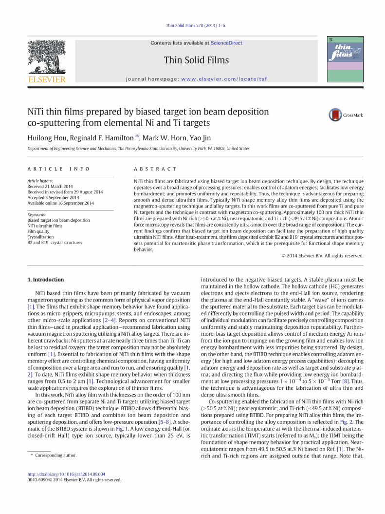
In this work, NiTi alloy filmwith thicknesses on the order of 100 nmare co-sputtered from separate Ni and Ti targets utilizing biased targetion beam deposition (BTIBD) technique. BTIBD allows differential bias-ing of each target BTIBD and combines ion beam deposition andsputtering deposition, and offers low-pressure operation [5–8]. A sche-matic of the BTIBD system is shown in Fig. 1. A low energy end-Hall (orclosed-drift Hall) type ion source, typically lower than 25 eV, is
introduced to the negative biased targets. A stable plasma must bemaintained in the hollow cathode. The hollow cathode (HC) generateselectrons and ejects electrons to the end-Hall ion source, renderingthe plasma at the end-Hall constantly stable. A “wave” of ions carriesthe sputteredmaterial to the substrate. Each target bias can bemodulat-ed differently by controlling the pulsedwidth and period. The capabilityof individualmodulation can facilitate precisely controlling compositionuniformity and stably maintaining deposition repeatability. Further-more, bias target deposition allows control of medium energy Ar ionsfrom the ion gun to impinge on the growing film and enables low ionenergy bombardment with less impurities being sputtered. By design,on the other hand, the BTIBD technique enables controlling adatom en-ergy (for high and low adatom energy process capabilities); decouplingadatom energy and deposition rate as well as target and substrate plas-ma; and directing the flux while providing low energy ion bombard-ment at low processing pressures 1 × 10⁻⁴ to 5 × 10⁻³ Torr [8]. Thus,the technique is advantageous for the fabrication of ultra thin anddense ultra smooth films.
Co-sputtering enabled the fabrication of NiTi thin films with Ni-rich(N50.5 at.% Ni); near equiatomic; and Ti-rich (b49.5 at.% Ni) composi-tions prepared using BTIBD. For preparing NiTi alloy thin films, the im-portance of controlling the alloy composition is reflected in Fig. 2. Theordinate axis is the temperature at with the thermal-induced martens-itic transformation (TIMT) starts (referred to asMs); the TIMT being thefoundation of shape memory behavior for practical application. Near-equiatomic ranges from 49.5 to 50.5 at.% Ni based on Ref. [1]. The Ni-rich and Ti-rich regions are assigned outside that range. Note that,
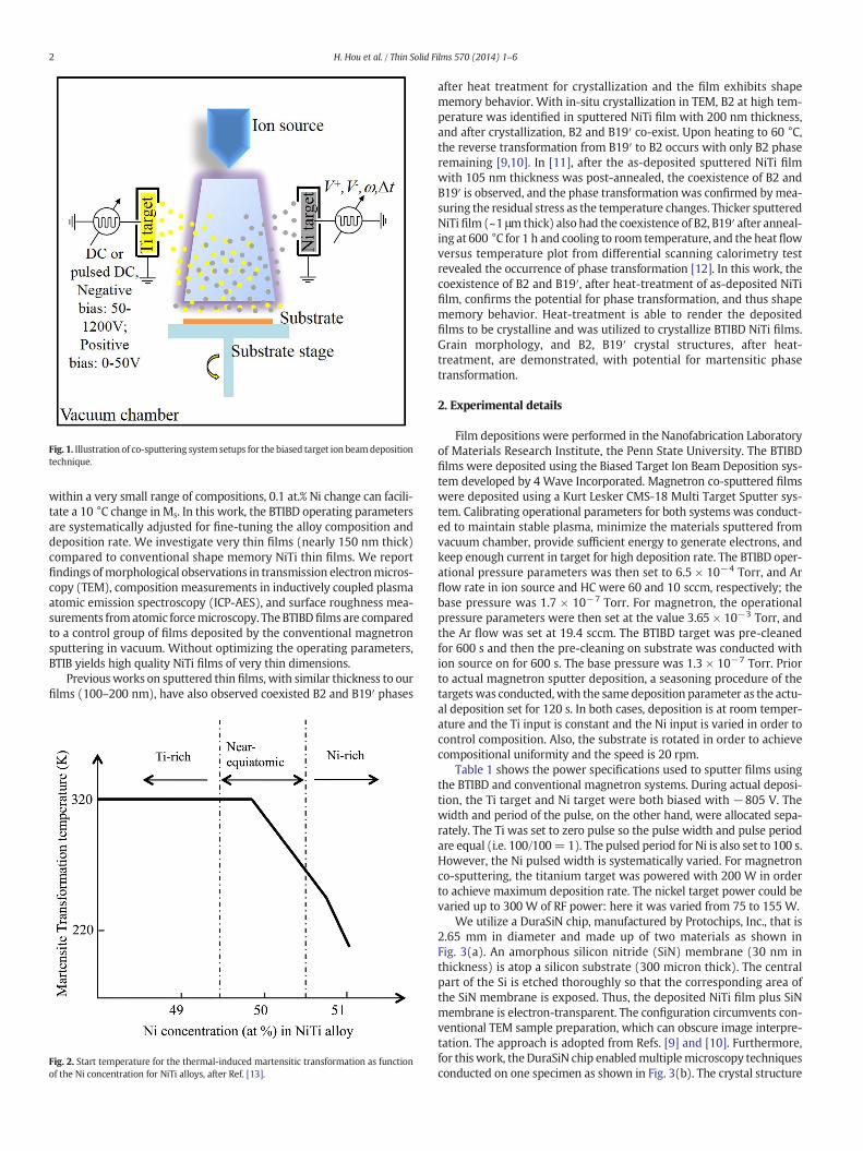
Fig. 1. Illustration of co-sputtering system setups for the biased target ion beamdepositiontechnique.
2 H. Hou et al. / Thin Solid Films 570 (2014) 1–6
within a very small range of compositions, 0.1 at.% Ni change can facili-tate a 10 °C change in Ms. In this work, the BTIBD operating parametersare systematically adjusted for fine-tuning the alloy composition anddeposition rate. We investigate very thin films (nearly 150 nm thick)compared to conventional shape memory NiTi thin films. We reportfindings ofmorphological observations in transmission electronmicros-copy (TEM), composition measurements in inductively coupled plasmaatomic emission spectroscopy (ICP-AES), and surface roughness mea-surements fromatomic forcemicroscopy. TheBTIBDfilms are comparedto a control group of films deposited by the conventional magnetronsputtering in vacuum. Without optimizing the operating parameters,BTIB yields high quality NiTi films of very thin dimensions.
Previous works on sputtered thin films, with similar thickness to ourfilms (100–200 nm), have also observed coexisted B2 and B19′ phases
Fig. 2. Start temperature for the thermal-induced martensitic transformation as functionof the Ni concentration for NiTi alloys, after Ref. [13].
after heat treatment for crystallization and the film exhibits shapememory behavior. With in-situ crystallization in TEM, B2 at high tem-perature was identified in sputtered NiTi film with 200 nm thickness,and after crystallization, B2 and B19′ co-exist. Upon heating to 60 °C,the reverse transformation from B19′ to B2 occurs with only B2 phaseremaining [9,10]. In [11], after the as-deposited sputtered NiTi filmwith 105 nm thickness was post-annealed, the coexistence of B2 andB19′ is observed, and the phase transformation was confirmed bymea-suring the residual stress as the temperature changes. Thicker sputteredNiTifilm (~1 μmthick) also had the coexistence of B2, B19′ after anneal-ing at 600 °C for 1 h and cooling to room temperature, and the heatflowversus temperature plot from differential scanning calorimetry testrevealed the occurrence of phase transformation [12]. In this work, thecoexistence of B2 and B19′, after heat-treatment of as-deposited NiTifilm, confirms the potential for phase transformation, and thus shapememory behavior. Heat-treatment is able to render the depositedfilms to be crystalline and was utilized to crystallize BTIBD NiTi films.Grain morphology, and B2, B19′ crystal structures, after heat-treatment, are demonstrated, with potential for martensitic phasetransformation.
2. Experimental details
Film depositions were performed in the Nanofabrication Laboratoryof Materials Research Institute, the Penn State University. The BTIBDfilms were deposited using the Biased Target Ion Beam Deposition sys-tem developed by 4 Wave Incorporated. Magnetron co-sputtered filmswere deposited using a Kurt Lesker CMS-18 Multi Target Sputter sys-tem. Calibrating operational parameters for both systems was conduct-ed to maintain stable plasma, minimize the materials sputtered fromvacuum chamber, provide sufficient energy to generate electrons, andkeep enough current in target for high deposition rate. The BTIBD oper-ational pressure parameters was then set to 6.5 × 10⁻⁴ Torr, and Arflow rate in ion source and HC were 60 and 10 sccm, respectively; thebase pressure was 1.7 × 10⁻⁷ Torr. For magnetron, the operationalpressure parameters were then set at the value 3.65 × 10⁻³ Torr, andthe Ar flow was set at 19.4 sccm. The BTIBD target was pre-cleanedfor 600 s and then the pre-cleaning on substrate was conducted withion source on for 600 s. The base pressure was 1.3 × 10⁻⁷ Torr. Priorto actual magnetron sputter deposition, a seasoning procedure of thetargetswas conducted, with the same deposition parameter as the actu-al deposition set for 120 s. In both cases, deposition is at room temper-ature and the Ti input is constant and the Ni input is varied in order tocontrol composition. Also, the substrate is rotated in order to achievecompositional uniformity and the speed is 20 rpm.
Table 1 shows the power specifications used to sputter films usingthe BTIBD and conventional magnetron systems. During actual deposi-tion, the Ti target and Ni target were both biased with −805 V. Thewidth and period of the pulse, on the other hand, were allocated sepa-rately. The Ti was set to zero pulse so the pulse width and pulse periodare equal (i.e. 100/100=1). The pulsed period for Ni is also set to 100 s.However, the Ni pulsed width is systematically varied. For magnetronco-sputtering, the titanium target was powered with 200 W in orderto achieve maximum deposition rate. The nickel target power could bevaried up to 300 W of RF power: here it was varied from 75 to 155 W.
We utilize a DuraSiN chip, manufactured by Protochips, Inc., that is2.65 mm in diameter and made up of two materials as shown inFig. 3(a). An amorphous silicon nitride (SiN) membrane (30 nm inthickness) is atop a silicon substrate (300 micron thick). The centralpart of the Si is etched thoroughly so that the corresponding area ofthe SiN membrane is exposed. Thus, the deposited NiTi film plus SiNmembrane is electron-transparent. The configuration circumvents con-ventional TEM sample preparation, which can obscure image interpre-tation. The approach is adopted from Refs. [9] and [10]. Furthermore,for thiswork, theDuraSiN chip enabledmultiplemicroscopy techniquesconducted on one specimen as shown in Fig. 3(b). The crystal structure
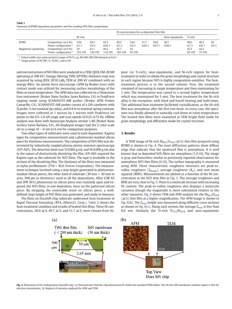
Table 1Summary of BTIBD deposition parameters and the resulting NiTi film compositions.
Ni concentration for as-deposited thin film
Ni-rich Near-equiatomic Ti-rich
BTIBD Composition (at.% Ni) 74.6 64.3 62.5 60.2 54.6 51.7 50.8 49.7 48.6 40.3 28Power configuration a 0.1:1 0.4:1 0.45:1 0.5:1 0.6:1 0.65:1 0.67:1 0.69:1 0.7:1 0.8:1 0.9:1
Magnetron sputtering Composition (at.% Ni) 70 61.1 60.2 55.7 52 47.2 42.2Power configuration b 155:195 120:195 110:195 105:195 95:195 85:195 75:195
a Pulsed width over pulse period in target of Ni:Ti, e.g. 40/100:100/100 denoted as 0.4:1.b Target power of Ni (RF) vs. Ti(DC), unit in W.
3H. Hou et al. / Thin Solid Films 570 (2014) 1–6
andmicrostructure of NiTifilmwere analyzed in a TEM (JEOL EM-2010Foperating at 200 kV). Energy-filtering TEM (EFTEM) thickness mapwasacquired by using JEOL 2010 LaB6 TEM at 200 kV combined with anenergy-filter. An atomic force microscope (AFM by Bruker Icon) withcontact mode was utilized for measuring surface morphology of thefilms at room temperature. The AFM data was collected on a DimensionIcon instrument (Bruker Nano Surface Santa Barbara, CA) in PeakForcetapping mode using SCANASYST-AIR probes (Bruker AFM ProbesCamarillo, CA). SCANASYST-AIR probes consist of a SiN cantilever withSi probe, 5 nmnominal tip radius, and 0.4 N/m nominal spring constant.Images were collected at 1 micron by 1 micron with PeakForce setpoints in the 0.5–1.0 nN range and scan speeds of 0.25–0.75 Hz. Offlineanalysis was done with Nanoscope Analysis version 1.40 (Bruker NanoSurface Santa Barbara, CA). All displayed images had the Z color scaleset to a range of −6 nm to 6 nm for comparison purposes.
Two other types of substrates were used in each deposition: Kaptontapes for composition measurements and a photoresist-masked siliconpiece for thicknessmeasurements. The composition of NiTi filmwas de-termined by inductively coupled plasma atomic emission spectroscopy(ICP-AES). The detection limit was Ti 0.002 g/mL and Ni 0.006 g/mL dueto the nature of destructively dissolving the film; ICP-AES required theKapton tape as the substrate for NiTi films. The tape is insoluble to theetchant of the dissolving film. The thickness of the films was measuredin stylus profilometer (P16+ KLA-Tencor Corporation). The measure-ment technique involved using a step height generated in photoresist-masked silicon pieces, the other kind of substrate (30 mm × 30 mm inarea, 500 μm in thickness) used in all the depositions. After LOR A5and SPR 3012 photoresist on silicon piece was routinely spun and ex-posed, the NiTi films, in one deposition, were on the patterned siliconpiece. By stripping the removable resist on silicon piece, a well-defined steps height of NiTi films was generated, and ready to measure.
The films on DuraSiN chip substrate underwent heat-treatment inRapid Thermal Annealing (RTA, Allwin21, Corp.). Table 2 shows theheat-treatment condition and results of heated thin films. Three Ni con-centrations, 28.0 at.%, 49.7 at.%, and 51.7 at.%, were chosen from Ni-
Fig. 3. Illustration of themultipurpose DuraSiN chip. (a) Demonstrates that the chip dimensionelectron transmission. (b) Regions of interests analyzed for AFM and TEM.
poor (or Ti-rich), near-equiatomic, and Ni-rich regions for heat-treatment in order to obtain the grainmorphology and crystal structurein each region because NiTi is highly composition-sensitive. The heat-treatment process is in the second column. First, the treatmentconsisted of increasing to target temperature and then maintaining for1 min. The temperature was raised to a second higher temperaturewhich was maintained for 5 min. The heat treatment for the Ni-richalloy is the exception; with third and fourth heating and hold times.This additional heat treatment facilitated crystallization, as the Ni-richfilm was amorphous after the first two heats. In every case, the speci-men was finally allowed to naturally cool down to room temperature.The heated thin films were examined in TEM bright field mode forgrain morphology and diffraction mode for crystal structure.
3. Results
A TEM image of Ni-rich Ni60.2Ti39.8 (at.%) thin film prepared usingBTIBD is shown in Fig. 4. The inset diffraction patterns show diffuserings that indicate that the sputtered film is amorphous. It is wellknown that as deposited NiTi films are amorphous [1,9,10]. The imageis gray and featureless similar to previously reported observations foramorphous NiTi thin films [9,10]. The surface topography is measuredusing AFM. Three characteristic roughness measures are peak-to-valley roughness (ZRange), average roughness (Ra), and root meansquared (RMS). Measurements are plotted as a function of the Ni con-centration in the NiTi thin film in Fig. 5. The average roughness andRMS are very close in Fig. 5. There is aminiscule increasewith increasingNi content. The peak-to-valley roughness also displays a minisculevariation though the magnitude is more substantial relative to theother measures. Fig. 6 shows TEM and AFM analysis for the Ni60.2Ti39.8(at.%) thin film at a higher magnification. The AFM image is shown inFig. 6(b). The Zmax height was measured along different cross-sectionsas shown in Fig. 6(c). Along each section, the average Zmax is less than0.6 nm. Similarly the Ti-rich Ti79.2Ni20.8 and near-equiatomic
s fit within the standard TEM holder. The 50mm SiNmembrane window region is thin for
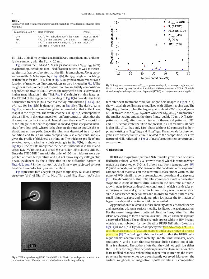
Table 2Summary of heat-treatment parameters and the resulting crystallographic phase in threeNiTi films.
Composition (at.% Ni) Heat-treatment Phases
28.0 450 °C for 1 min, then 500 °C for 5 min B2, B19′, Ti2Ni49.7 450 °C 1 min, then 500 °C for 5 min B19′, Ti2Ni51.7 450 °C 1 min, 500 °C 5 min, 500 °C 3 min,
and then 515 °C for 3 minB2, B19′
Fig. 5. Roughness measurements (Zrange = peak-to-valley; Ra = average roughness; andRMS= root mean squared) as a function of the at.% Ni concentration in NiTi for films fab-ricated using biased target ion beam deposited (BTIBD) and magnetron sputtering (MS).
4 H. Hou et al. / Thin Solid Films 570 (2014) 1–6
Ti51.4Ni48.6 thin films synthesized in BTIBD are amorphous and uniform-ly ultra-smooth, with the Zmax b 0.6 nm.
Fig. 7 shows the TEM and AFM analysis for a Ni-rich Ni55.7Ti44.3 (at.%)magnetron sputtered thin film. The diffraction pattern, aswell as the fea-tureless surface, corroborates that the film is amorphous. Along cross-sections of the AFM topography in Fig. 7(b), the Zmax height ismuch larg-er than those for the BTIBD film in Fig. 6. Roughness measurements as afunction of magnetron film composition are also included in Fig. 5. Theroughness measurements of magnetron film are highly composition-dependent relative to BTIBD. When the magnetron film is viewed at ahigher magnification in the TEM, Fig. 8(a) exhibits striking features.The EFTEM of the region corresponding to Fig. 8(b) provides the localnormalized thickness (t/λ) map via the log-ratio method [14,15]. Thet/λ map for Fig. 8(b) is demonstrated in Fig. 8(c). The dark area inFig. 8(a) allows less beam through to be recorded so that in thicknessmap it is the brightest. The white channels in Fig. 8(a) correspond tothe dark lines in thickness map. Non-uniform contrasts reflect that thethickness in the dark area and channel is not the same. The logarithmof the integral of the entire spectrum is divided by the integrated inten-sity of zero-loss peak,where t is the absolute thicknesses and λ is the in-elastic mean free path. Since the film was deposited in a rotatedcondition and thus a uniform composition, λ is a constant, and t/λgives the profile of thickness distribution. The thickness profile of oneselected area, marked as a dash rectangle in Fig. 8(b), is shown inFig. 8(c). The results imply that the densest material is in the islandareas. Relative to the island areas, we consider the channels unfilled.Since the BTIBD NiTi films with the order of 100 nm thickness were de-posited at room temperature and did not show any crystallographicphase, evidenced by the diffuse ring in the diffraction pattern ofFigs. 4, 6, and 7 in the manuscript, the films were subjected to heattreatments in order to crystallize the films.
Fig. 9 presents TEM analysis on grain morphology (a–c) and crystalstructure (d–f) of Ni28.0Ti72.0, Ni49.7Ti50.3 and Ni51.7Ti48.3 (at.%) thin
Fig. 4. TEM image showing BTIBD Ni-rich NiTi thin film in the as-deposited state at roomtemperature. Inset diffraction pattern which does not reflect crystallinity.
film after heat-treatment condition. Bright-field images in Fig. 9 (a–c)show that all three films are crystallized with different grain sizes. TheNi49.7Ti50.3 film in (b) has the largest grains, about ~200 nm, and grainsof 120 nm are in the Ni28.0Ti72.0 filmwhile the Ni51.7Ti48.3 film producedthe smallest grains among the three films, roughly 70 nm. Diffractionpatterns in (d–f), after overlapping with theoretical patterns of B2,and B19′, demonstrate that B19′ are present in all three films. Of noteis that Ni49.7Ti50.3 has only B19′ phase without B2 compared to bothphases existing in Ni28.0Ti72.0 and Ni51.7Ti48.3. The rationale for observedgrains size and crystal structure is related to the composition-sensitivenature of NiTi, reflected in Fig. 2 of transformation temperature andcomposition.
4. Discussion
BTIBD and magnetron sputtered NiTi thin film growth can be classi-fied in the Volmer–Weber (VW)growthmodel,which is commonwhenmetals are deposited on SiO2 and grown near room temperature [16].Physical vapor deposition (PVD) involves the condensation of vaporizedcomponent of materials on the substrate surface under vacuum. Thestages of PVD thin film growth are nucleation, growth, and coalescence[16]. The deposition of thin solid film commences with a nucleationstage and clusters of atoms form islands on the substrate surface. Agrowth stage follows as deposition continues, in which islands take onimpinging atoms and grow as nuclei until they reach a sub-criticalsize. A coalescence stage follows and in order to reduce surface area,small islands coalesce and agglomeration facilitates the formation ofbigger islands until a continuous film is deposited.
Agglomeration is related to surface mobility of the adsorbed speciesand increasing adatom's surface mobility facilitates the agglomeration.For the current magnetron sputtered ultrathin films, rather than theislands coalescing to form a continuous film, unfilled channels separatea network of islands. The unfilled channels appear white in TEM images,which are not obvious for the ultrathin BTIBD NiTi films (compareFigs. 3(d) and 4(d)). Hylton et al. specify that two advantages of BTIBDtechnique are control of adatom energies and a large range of processpressures [8]. The findings in this work confirm that the BTIBD tech-nique enables adatom surface mobility (and thus mass transfer) of co-sputtered Ni and Ti such that coalescence during deposition of NiTifilms is enhanced. The authors note that they did not optimize eithertheBTIBDor themagnetron deposition parameters tominimize or elim-inate unfilled channels. When using magnetron sputtering, the micro-structural heterogeneities were consistently observed. Moreover, thesurface roughness of magnetron sputtered films is composition
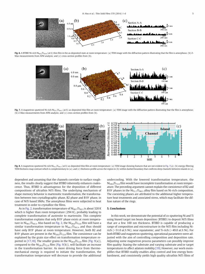
Fig. 6. A BTIBD Ni-rich Ni60.2Ti39.8 (at.%) thin film in the as-deposited state at room temperature: (a) TEM imagewith the diffraction pattern illustrating that the film is amorphous; (b) Z-Max measurements from AFM analysis; and (c) cross-section profiles from (b).
Fig. 7. A magnetron sputtered Ni-rich Ni55.7Ti44.3 (at.%) as-deposited thin film at room temperature: (a) TEM image with the diffraction pattern illustrating that the film is amorphous;(b) Z-Max measurements from AFM analysis; and (c) cross-section profiles from (b).
Fig. 8. Amagnetron sputtered Ni-rich Ni55.7Ti44.3 (at.%) as-deposited thin film at room temperature: (a) TEM image showing features that are not evident in Fig. 7(a); (b) energy-filteringTEM thicknessmap contrastwhich is complementary to (a); and (c) thickness profile across the region in (b)within dashed boundary that confirms deep channels between islands in (a).
5H. Hou et al. / Thin Solid Films 570 (2014) 1–6
dependent and assuming that the channels correlate to surface rough-ness, the results clearly suggest that BTIBD inherently enhances coales-cence. Thus, BTIBD is advantageous for the deposition of differentcompositions of ultrathin NiTi films. The underlying mechanism ofshape memory behavior is martensitic transformation, the transforma-tion between two crystallographic phase, B2 phase and B19′ phase, incase of NiTi based SMAs. The amorphous films were subjected to heattreatment in order to crystallize the films.
As in Fig. 2, transformation temperature of Ni49.7Ti50.3 is about 320 Kwhich is higher than room temperature (294 K), probably leading tocomplete transformation of austenite to martensite. This completetransformation explains that only B19′ phase exists at room tempera-ture in Ni49.7Ti50.3. Also based on Fig. 2, the Ni28.0Ti72.0 film will have asimilar transformation temperature to Ni49.7Ti50.3, and thus shouldhave only B19′ phase at room temperature. However, both B2 andB19′ phases are present in the Ni28.0Ti72.0 film. The coexistence can beexplained by the grain size effect on transformation temperature re-ported in [17,18]. The smaller grains in the Ni28.0Ti72.0 film (Fig. 9(a)),compared to the Ni28.0Ti72.0 film (Fig. 9(b)), will facilitate an increasein the transformation barrier. As more driving force from thermo-mechanical energy is required to initiate the transformation, thetransformation temperature will decrease to provide the additional
undercooling. With the lowered transformation temperature, theNi28.0Ti72.0filmwould have incomplete transformation at room temper-ature. The preceding argument cannot explain the coexistence of B2 andB19′ phases in the Ni51.7Ti48.3 alloy film based on Ni-rich composition.The coexisting phases are attributed to the additional higher tempera-ture heat treatments and associated stress, whichmay facilitate the dif-fuse nature of the rings.
5. Conclusions
In thiswork, we demonstrate the potential of co-sputteringNi and Tiusing biased target ion beam deposition (BTIBD) to deposit NiTi filmsthat are a few 100 nm thickness. BTIBD is capable of producing arange of composition and microstructure in the NiTi film including Ni-rich (N51.0 at.% Ni); near equiatomic; and Ti-rich (b49.0 at.% Ni). Forboth BTIBD andmagnetron sputtering, operational parameterswere ad-justed with the aim of controlling composition and deposition rate.Adjusting some magnetron process parameters can possibly improvefilm quality: biasing the substrate and varying substrate and/or targettemperatures to affect adatommobility [19]. However, our work exem-plifies that BTIBD readily enables alloy control and low energy bom-bardment, and consistently yields high quality ultrathin NiTi films of
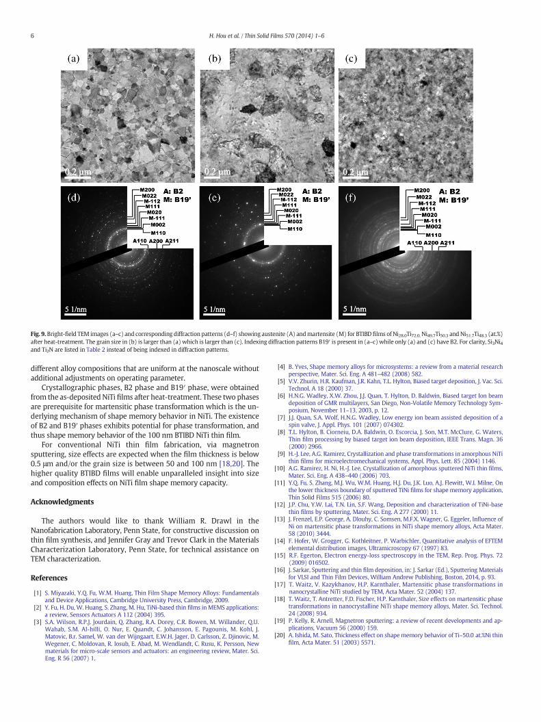
Fig. 9.Bright-field TEM images (a–c) and corresponding diffraction patterns (d–f) showing austenite (A) andmartensite (M) for BTIBD films of Ni28.0Ti72.0, Ni49.7Ti50.3 andNi51.7Ti48.3 (at.%)after heat-treatment. The grain size in (b) is larger than (a) which is larger than (c). Indexing diffraction patterns B19′ is present in (a–c) while only (a) and (c) have B2. For clarity, Si3Ni4and Ti2N are listed in Table 2 instead of being indexed in diffraction patterns.
6 H. Hou et al. / Thin Solid Films 570 (2014) 1–6
different alloy compositions that are uniform at the nanoscale withoutadditional adjustments on operating parameter.
Crystallographic phases, B2 phase and B19′ phase, were obtainedfrom the as-deposited NiTi films after heat-treatment. These two phasesare prerequisite for martensitic phase transformation which is the un-derlying mechanism of shape memory behavior in NiTi. The existenceof B2 and B19′ phases exhibits potential for phase transformation, andthus shape memory behavior of the 100 nm BTIBD NiTi thin film.
For conventional NiTi thin film fabrication, via magnetronsputtering, size effects are expected when the film thickness is below0.5 μm and/or the grain size is between 50 and 100 nm [18,20]. Thehigher quality BTIBD films will enable unparalleled insight into sizeand composition effects on NiTi film shape memory capacity.
Acknowledgments
The authors would like to thank William R. Drawl in theNanofabrication Laboratory, Penn State, for constructive discussion onthin film synthesis, and Jennifer Gray and Trevor Clark in the MaterialsCharacterization Laboratory, Penn State, for technical assistance onTEM characterization.
References
[1] S. Miyazaki, Y.Q. Fu, W.M. Huang, Thin Film Shape Memory Alloys: Fundamentalsand Device Applications, Cambridge University Press, Cambridge, 2009.
[2] Y. Fu, H. Du, W. Huang, S. Zhang, M. Hu, TiNi-based thin films inMEMS applications:a review, Sensors Actuators A 112 (2004) 395.
[3] S.A. Wilson, R.P.J. Jourdain, Q. Zhang, R.A. Dorey, C.R. Bowen, M. Willander, Q.U.Wahab, S.M. Al-hilli, O. Nur, E. Quandt, C. Johansson, E. Pagounis, M. Kohl, J.Matovic, B.r. Samel, W. van der Wijngaart, E.W.H. Jager, D. Carlsson, Z. Djinovic, M.Wegener, C. Moldovan, R. Iosub, E. Abad, M. Wendlandt, C. Rusu, K. Persson, Newmaterials for micro-scale sensors and actuators: an engineering review, Mater. Sci.Eng. R 56 (2007) 1.
[4] B. Yves, Shape memory alloys for microsystems: a review from a material researchperspective, Mater. Sci. Eng. A 481–482 (2008) 582.
[5] V.V. Zhurin, H.R. Kaufman, J.R. Kahn, T.L. Hylton, Biased target deposition, J. Vac. Sci.Technol. A 18 (2000) 37.
[6] H.N.G. Wadley, X.W. Zhou, J.J. Quan, T. Hylton, D. Baldwin, Biased target Ion beamdeposition of GMR multilayers, San Diego, Non-Volatile Memory Technology Sym-posium, November 11–13, 2003, p. 12.
[7] J.J. Quan, S.A. Wolf, H.N.G. Wadley, Low energy ion beam assisted deposition of aspin valve, J. Appl. Phys. 101 (2007) 074302.
[8] T.L. Hylton, B. Ciorneiu, D.A. Baldwin, O. Escorcia, J. Son, M.T. McClure, G. Waters,Thin film processing by biased target ion beam deposition, IEEE Trans. Magn. 36(2000) 2966.
[9] H.-J. Lee, A.G. Ramirez, Crystallization and phase transformations in amorphous NiTithin films for microelectromechanical systems, Appl. Phys. Lett. 85 (2004) 1146.
[10] A.G. Ramirez, H. Ni, H.-J. Lee, Crystallization of amorphous sputtered NiTi thin films,Mater. Sci. Eng. A 438–440 (2006) 703.
[11] Y.Q. Fu, S. Zhang, M.J. Wu, W.M. Huang, H.J. Du, J.K. Luo, A.J. Flewitt, W.I. Milne, Onthe lower thickness boundary of sputtered TiNi films for shape memory application,Thin Solid Films 515 (2006) 80.
[12] J.P. Chu, Y.W. Lai, T.N. Lin, S.F. Wang, Deposition and characterization of TiNi-basethin films by sputtering, Mater. Sci. Eng. A 277 (2000) 11.
[13] J. Frenzel, E.P. George, A. Dlouhy, C. Somsen, M.F.X. Wagner, G. Eggeler, Influence ofNi on martensitic phase transformations in NiTi shape memory alloys, Acta Mater.58 (2010) 3444.
[14] F. Hofer, W. Grogger, G. Kothleitner, P. Warbichler, Quantitative analysis of EFTEMelemental distribution images, Ultramicroscopy 67 (1997) 83.
[15] R.F. Egerton, Electron energy-loss spectroscopy in the TEM, Rep. Prog. Phys. 72(2009) 016502.
[16] J. Sarkar, Sputtering and thin film deposition, in: J. Sarkar (Ed.), Sputtering Materialsfor VLSI and Thin Film Devices, William Andrew Publishing, Boston, 2014, p. 93.
[17] T. Waitz, V. Kazykhanov, H.P. Karnthaler, Martensitic phase transformations innanocrystalline NiTi studied by TEM, Acta Mater. 52 (2004) 137.
[18] T. Waitz, T. Antretter, F.D. Fischer, H.P. Karnthaler, Size effects on martensitic phasetransformations in nanocrystalline NiTi shape memory alloys, Mater. Sci. Technol.24 (2008) 934.
[19] P. Kelly, R. Arnell, Magnetron sputtering: a review of recent developments and ap-plications, Vacuum 56 (2000) 159.
[20] A. Ishida, M. Sato, Thickness effect on shape memory behavior of Ti–50.0 at.%Ni thinfilm, Acta Mater. 51 (2003) 5571.
Copyright © 2022 FDOKUMEN