International Technology Roadmap for Semiconductors 2002 ...
194
International Technology Roadmap for Semiconductors 2002 Update Jointly Sponsored by European Semiconductor Industry Association Japan Electronics and Information Technology Industries Association Korea Semiconductor Industry Association Taiwan Semiconductor Industry Association Semiconductor Industry Association
-
Upload
khangminh22 -
Category
Documents
-
view
2 -
download
0
Transcript of International Technology Roadmap for Semiconductors 2002 ...

International Technology Roadmap for Semiconductors
2002 Update
Jointly Sponsored
by
European Semiconductor Industry Association
Japan Electronics and Information Technology Industries Association
Korea Semiconductor Industry Association
Taiwan Semiconductor Industry Association
Semiconductor Industry Association

THE INTERNATIONAL TECHNOLOGY ROADMAP FOR SEMICONDUCTORS: 2002 UPDATE
INTERNATIONAL TECHNOLOGY ROADMAP
FOR SEMICONDUCTORS
2002 UPDATE


i
THE INTERNATIONAL T ECHNOLOGY ROADMAP FOR SEMICONDUCTORS: 2002 U PDATE
T ABLE OF CONTENTS
Foreword ................................................................................................................................ i
Introduction [from the 2001 ITRS] .................................................................................. 1
Overview ............................................................................................................................... 1 Meaning of ITRS Technology Requirements ....................................................................... 1 Position on Potential Solutions ............................................................................................. 2 Overall Roadmap Process and Structure............................................................................. 2
Technology Characteristics / Requirements Ta bles .................................................................4 Technology Nodes ................................................................................................................6 Drivers for ITWG Technology Requirements...........................................................................7
Grand Challenges ............................................................................................................... 9
Overview ............................................................................................................................... 9 In the Near Term (through 2007) .......................................................................................... 9
Enhancing Performance........................................................................................................9 Cost-effective Manufacturing ............................................................................................... 11
In The Long Term (2008 through 2016) ............................................................................. 14 Enhancing Performance...................................................................................................... 14 Cost-effective Manufacturing ............................................................................................... 14
2002 Update Tables .......................................................................................................... 16
Design ................................................................................................................................. 16 Test ..................................................................................................................................... 19 Process Integration, Devices, and Structures .................................................................... 29 Front End Processes .......................................................................................................... 45 Lithography ......................................................................................................................... 63 Interconnect ........................................................................................................................ 74 Factory Integration .............................................................................................................. 79 Assembly and Packaging ................................................................................................. 100 Environment, Safety, and Health ...................................................................................... 112 Yield Enhancement........................................................................................................... 117 Metrology .......................................................................................................................... 134 Modeling and Simulation .................................................................................................. 143
Overall Roadmap Technology Characteristics .......................................................150
Background ....................................................................................................................... 150 Overview of 2001 Revisions ............................................................................................. 150
Definitions ........................................................................................................................ 150 Roadmap Timeline ........................................................................................................... 150 Product Generations and Chip -Size Model ......................................................................... 154 Chip -Size, Lithographic- Field, and Wafer -Size Trends ........................................................ 161 Performance of Packaged Chips ....................................................................................... 164 Electrical Defect Density ................................................................................................... 169 Power Supply and Power Dissipation................................................................................. 170 Cost................................................................................................................................. 171

ii
THE INTERNATIONAL TECHNOLOGY ROADMAP FOR SEMICONDUCTORS: 2002 UPDATE
Glossary ............................................................................................................................174 Characteristics of Major Markets........................................................................................ 174 Chip and Package—Physical and Electrical Attributes ........................................................ 176 Fabrication Attributes And Methods ................................................................................... 177 Maximum Substrate Diameter (mm) ................................................................................... 177 Electrical Design And Test Metrics..................................................................................... 177 Design and Test ............................................................................................................... 177 Add ................................................................................................................................. 177 Tec hnology Requirements Solutions .................................................................................. 177
LIST OF FIGURES
Figure 1 Composition of the Technology Working Group (TWG)....................................... 3 Figure 2 A Typical Production “Ramp” Curve ..................................................................... 5 Figure 3 Technology Node Compared to Actual Production Capacity Technology Distribution ............................................ 6 Figure 4 Definition of the Half Pitch and Gate Length ........................................................ 7 Figure 5 MOS Transistor Scaling—1974 to present ....................................................... 152 Figure 6 Scaling Calculator ............................................................................................. 152 Figure 7 ITRS Roadmap Acceleration Continues —Half Pitch Trends ........................... 153 Figure 8 ITRS Roadmap Acceleration Continues —Gate Length Trends ....................... 153
LIST OF INTRODUCTION TABLES
Table A Improvement Trends for ICs Enabled by Feature Scaling .................................... 1 Table B ITRS Table Structure—Key Lithography-Related Characteristics by Product Type .................................................................................................... 4 Table C Rounded versus Actual Trend Numbers ........................................................... 151

iii
THE INTERNATIONAL TECHNOLOGY ROADMAP FOR SEMICONDUCTORS: 2002 UPDATE
LIST OF OVERALL ROADMAP TECHNOLOGY CHARACTERISTICS TABLES
Table 1a Product Generations and Chip Size Model Technology Nodes — Near-term Years ............................................................................................... 155 Table 1b Product Generations and Chip Size Model Technology Nodes — Long-term years ............................................................................................... 155 Table 1c DRAM Production Product Generations and Chip Size Model— Near-term Years ............................................................................................... 156 Table 1d DRAM Production Product Generations and Chip Size Model— Long-term Years ............................................................................................... 156 Table 1e DRAM Introduction Product Generations and Chip Size Model— Near-term Years ............................................................................................... 157 Table 1f DRAM Introduction Product Generations and Chip Size Model— Long-term Years ................................................................................................ 157 Table 1g MPU (High-volume Microprocessor) Cost-Performance Product Generations and Chip Size Model— Near-term Years ...................... 158 Table 1h MPU (High-volume Microprocessor) Cost-Performance Product Generations and Chip Size Model—Long-term Years....................... 159 Table 1i High-Performance MPU and ASIC Product Generations and Chip Size Model—Near-term Years ........................ 160 Table 1j High-Performance MPU and ASIC Product Generations and Chip Size Model—Long-term Years........................ 160 Table 2a Lithographic -Field and Wafer-Size Trends —Near-term Years ....................... 163 Table 2b Lithographic -Field and Wafer Size Trends —Long-term Years ....................... 163 Table 3a Performance of Packaged Chips: Number of Pads and Pins —Near-term Years ................................................. 164 Table 3b Performance of Packaged Chips: Number of Pads and Pins —Long-term Years ................................................. 165 Table 4a Performance and Package Chips: Pads, Cost— Near-term Years [Update] ............................................................................... 166 Table 4b Performance and Package Chips: Pads, Cost— Long-term Years [Update] ............................................................................... 167 Table 4c Performance and Package Chips: Frequency On-Chip Wiring Levels — Near-term Years [Update] ............................................................................... 167 Table 4d Performance and Package Chips: Frequency, On-Chip Wiring Levels — Long-term Years [Update] ............................................................................... 168 Table 5a Electrical Defects —Near-term Years ............................................................... 169 Table 5b Electrical Defects —Long-term Years............................................................... 169 Table 6a Power Supply and Power Dissipation—Near-term Years ............................... 170 Table 6b Power Supply and Power Dissipation—Long-term Years ............................... 170 Table 7a Cost—Near-term Years .................................................................................... 172 Table 7b Cost—Long-term Years.................................................................................... 173

iv
THE INTERNATIONAL TECHNOLOGY ROADMAP FOR SEMICONDUCTORS: 2002 UPDATE
LIST OF DIFFICULT CHALLENGES TABLES
Table 13 Design Difficult Challenges ................................................................................ 16 Table 19 Test Difficult Challenges ..................................................................................... 19 Table 34 Process Integration Difficult Challenges [Update]............................................. 29 Table 48 Front End Processes Difficult Challenges ......................................................... 45 Table 56 Lithography Difficult Challenges ........................................................................ 63 Table 61 Interconnect Difficult Challenges [Update] ........................................................ 74 Table 65 Factory Integration Difficult Challenges [Update].............................................. 79 Table 74 Assembly and Packaging Difficult Challenges [Update] ................................. 100 Table 82 Environment, Safety, and Health Difficult Challenges ..................................... 112 Table 88 Yield Enhancement Difficult Challenges .......................................................... 117 Table 96 Metrology Difficult Challenges .......................................................................... 134 Table 102 Modeling and Simulation Difficult Challenges [Update] ................................ 143
LIST OF 2002 ITRS UPDATED TECHNOLOGY REQUIREMENTS TABLES
SYSTEM DRIVERS Tables 8–12 are unchanged for the 2002 Update [Refer to the 2001 ITRS System Drivers chapter]
Figure 10 First Integration of Technologies on SOC with Standard CMOS Process....... 17
DESIGN Tables 13–18 are unchanged for the 2002 Update. [Refer to the 2001 ITRS Design chapter]
TEST
Tables 19–22, 24–27, 29, 31, and 33 are unchanged for the 2002 Update [Refer to the 2001 ITRS Test chapter]
Table 23a High Frequency Serial Communications Test Requirements —Near-term....................................................................... 21 Table 28 DFT-BIST Device Test Requirements —Near-term** ........................................ 22 Table 30a Commodity Flash Memory Test Requirements —Near-term ........................... 25 Table 30b Commodity Flash Memory Test Requirements —Long-term........................... 26 Table 32a Burn- in Requirements —Near-term .................................................................. 27 Table 32b Burn- in Requirements —Long-term .................................................................. 28

v
THE INTERNATIONAL TECHNOLOGY ROADMAP FOR SEMICONDUCTORS: 2002 UPDATE
PROCESS INTEGRATION
Table 34 is the update of Process Integration Difficult Challenges Tables 39-48 are unchanged for the 2002 Update [Refer to the 2001 ITRS Process Integration chapter]
Table 35a High-performance Logic Technology Requirements —Near-term ................... 31 Table 35b High-performance Logic Technology Requirements —Long-term................... 32 Table 36a Low Operating Power (LOP) Logic Technology Requirements —Near-term ........................................................... 35 Table 36b Low Operating Power (LOP) Logic Technology Requirements —Long-term........................................................... 36 Table 36c Low Standby Power (LSTP) Technology Requirements —Near-term ........................................................... 37 Table 36d Low Standby Power (LSTP) Technology Requirements —Long-term........................................................... 38 Table 37a DRAM Technology Requirements —Near-term ............................................... 41 Table 37b DRAM Technology Requirements —Long-term ............................................... 41 Table 38a Non- Volatile Memory Technology Requirements —Near-term........................ 43 Table 38b Non- Volatile Memory Technology Requirements —Long-term........................ 44
FRONT END PROCESSES Tables 48, 52, 55, and 56 are unchanged for the 2002 Update [Refer to the 2001 ITRS Front End Processes chapter]
Table 49a Starting Materials Technology Requirements —Near-term ............................. 48 Table 49b Starting Materials Technology Requirements —Long-term ............................. 50 Table 50a Surface Preparation Technology Requirements*—Near-term ........................ 52 Table 50b Surface Preparation Technology Requirements*—Long-term........................ 53 Table 51a Thermal & Thin Film, Doping and Etching Technology Requirements —Near-term ........................................................... 56 Table 51b Thermal & Thin Film, Doping and Etching Technology Requirements —Long-term........................................................... 58 Table 53a DRAM Trench Capacitor Technology Requirements —Near-term ........................................................... 60 Table 54a FLASH Non-volatile Memory Technology Requirements —Near-term ........................................................... 61 Table 54b FLASH Non-volatile Memory Technology Requirements —Long-term........................................................... 62

vi
THE INTERNATIONAL TECHNOLOGY ROADMAP FOR SEMICONDUCTORS: 2002 UPDATE
LITHOGRAPHY
Tables 58 and 60 are unchanged for the 2002 Update [Refer to the 2001 ITRS Lithography chapter]
Table 57a Lithography Technology Requirements —Near-term....................................... 64 Table 57b Lithography Technology Requirements —Long-term....................................... 65 Table 59a Optical Mask Requirements ............................................................................. 66 Table 59b EUVL Mask Requirements ............................................................................... 69 Table 59c EPL Mask Requirements .................................................................................. 71
INTERCONNECT
Table 61 is the update of Interconnect Difficult Challenges Table 64 is unchanged for the 2002 Update [Refer to the 2001 ITRS Interconnect chapter]
Table 62a MPU Interconnect Technology Requirements —Near-term............................. 75 Table 62b MPU Interconnect Technology Requirements —Long-term ............................ 76 Table 63a DRAM Interconnect Technology Requirements —Near-term .......................... 77 Table 63b DRAM Interconnect Technology Requirements —Long-term.......................... 78
FACTORY INTEGRATION Table 65 is the update of Factory Integration Difficult Challenges Tables 72–73 are unchanged for the 2002 Update [Refer to the 2001 ITRS Factory Integration chapter]
Table 66a Factory Operations Technology Requirements —Near-term........................... 81 Table 66b Factory Operations Technology Requirements —Long-term........................... 82 Table 67a Production Equipment Technology Requirements —Near-term ...................... 84 Table 67b Production Equipment Technology Requirements —Long-term...................... 85 Table 68a Material Handling Systems Technology Requirements —Near-term (40K WSPM) [7]................................ 88 Table 68b Material Handling Systems Technology Requirements —Long-term (40K WSPM) [7] ............................... 89 Table 69a Factory Information and Control Systems Technology Requirements —Near-term[1] ....................................................... 92 Table 69b Factory Information and Control Systems Technology Requirements —Long-term[1]....................................................... 93 Table 70a Facilities Technology Requirements —Near-term............................................ 95 Table 70b Facilities Technology Requirements —Long-term............................................ 96 Table 71a Probe/Test Manufacturing Technology Requirements —Near-term................ 98 Table 71b Probe/Test Manufacturing Technology Requirements —Long-term................ 98

vii
THE INTERNATIONAL TECHNOLOGY ROADMAP FOR SEMICONDUCTORS: 2002 UPDATE
ASSEMBLY AND PACKAGING
Table 74 is the update of Assembly and Packaging Difficult Challenges Table 81 is unchanged for the 2002 Update [Refer to the 2001 ITRS Assembly and Packaging chapter]
Table 75a Single-chip Packaging Technology Requirements —Near-term.................... 102 Table 75b Single-chip Packaging Technology Requirements —Long-term ................... 105 Table 76 Comparison between Bare Chip Mounting and WLP Technology .................. 108 Table 77 Chip to Next Level Potential Solutions ............................................................. 109 Table 78 Ball Grid Array Packages Potential Solutions .................................................. 110 Table 79 Single Chip Packages Potential Solutions ....................................................... 111 Table 80 BGA and FBGA/CSP Package Substrate Potential Solutions ........................ 111
ENVIRONMENT, SAFETY, AND HEALTH Tables 82 and 85–87 are unchanged for the 2002 Update [Refer to the 2001 ITRS ESH chapter]
Table 83a ESH Intrinsic Requirements —Near-term....................................................... 113 Table 84a Chemicals, Materials and Equipment Management Technology Requirements —Near-term ......................................................... 115
YIELD ENHANCEMENT
Tables 88 and 92 are unchanged for the 2002 Update [Refer to the 2001 ITRS Yield Enhancement chapter]
Table 89 Defect Budget Technology Requirement Assumptions ................................... 118 Table 90 Yield Model and Defect Budget MPU Technology Requirements .................. 119 Table 91 Yield Model and Defect Budget DRAM Technology Requirements ................ 121 Table 93a Defect Detection Technology Requirements —Near-term ............................. 123 Table 93b Defect Detection Technology Requirements —Long-term............................. 124 Table 94a Yield Learning Technology Requirements —Near-term................................. 126 Table 94b Yield Learning Technology Requirements —Long-term ................................ 127 Table 95a Wafer Environmental Contamination Control Technology Requirements —Near-term ......................................................... 129 Table 95b Wafer Environmental Contamination Control Technology Requirements —Long-term........................................................ 131

viii
THE INTERNATIONAL TECHNOLOGY ROADMAP FOR SEMICONDUCTORS: 2002 UPDATE
METROLOGY Tables 96 and 99 are unchanged for the 2002 Update [Refer to the 2001 ITRS Metrology chapter]
Table 97a Metrology Technology Requirements —Near-term ........................................ 135 Table 97b Metrology Technology Requirements —Long-term........................................ 136 Table 98a Lithography Wafer Metrology Technology Requirements —Near-term ......................................................... 137 Table 98b Lithography Metrology Technology Requirements —Long-term ................... 138 Table 100a Front End Processes Metrology Technology Requirements —Near-term ....................................................... 139 Table 100b Front End Processes Metrology Technology Requirements —Long-term....................................................... 140 Table 101a Interconnect Metrology Technology Requirements —Near Term................ 141 Table 101b Interconnect Metrology Technology Requirements —Long-term ................ 142
MODELING AND SIMULATION
Table 102 is the update of Modeling and Simulation Difficult Challenges [Refer to the 2001 ITRS Modeling and Simulation chapter].
Table 103a Modeling and Simulation Technology Requirements: Capabilities —Near-term ............................................................................... 145 Table 103b Modeling and Simulation Technology Requirements: Accuracy and Speed—Near-term ................................................................ 147 Table 103c Modeling and Simulation Technology Requirements: Capabilities —Long-term............................................................................... 149 Contact Information for the IT RS.................................................................................. 178

Foreword i
THE INTERNATIONAL TECHNOLOGY ROADMAP FOR SEMICONDUCTORS: 2002 UPDATE
FOREWORD The International Technology Roadmap for Semiconductors (ITRS) is the result of a worldwide consensus building process. This document predicts the main trends in the semiconductor industry spanning across 15 years into the future. The participation of experts from Europe, Japan, Korea, and Taiwan as well as the U.S.A. ensures that the ITRS is a valid source of guidance for the semiconductor industry as we strive to extend the historical advancement of semiconductor technology and the worldwide integrated circuit (IC) market. These five regions jointly sponsor the ITRS.
The Semiconductor Industry Association (SIA) coordinated the first efforts of producing what was originally The National Technology Roadmap for Semiconductors (NTRS). The NTRS provided a 15-year outlook on the major trends of the semiconductor industry. As such, it was a good reference document for all semiconductor manufacturers. Most of all, the NTRS documents provided useful guidance for suppliers of equipment, materials, and software and clear targets for researchers in the outer years.
The semiconductor industry became a global industry in the 1990s, as many semiconductor chip manufacturers established manufacturing or assembly facilities in multiple regions of the world. Similarly, the suppliers to the semiconductor industry have established worldwide operations. Furthermore, alliances, joint ventures, and many forms of cooperation have been established among semiconductor manufacturers as well as among equipment, materials, and software suppliers.
The above considerations led to the realization that a Roadmap that provides guidance for the whole industry would benefit from inputs from all regions of the world that have leadership activities in the field of semiconductors. This realization has led to the creation of the International Technology Roadmap for Semiconductors (ITRS). The invitation to cooperate on the ITRS was extended by the SIA at the World Semiconductor Council in April of 1998 to Europe, Japan, Korea, and Taiwan. The initial collaboration of these five regions produced the ITRS 1998 Update, which consisted of a comprehensive revision of the 1997 NTRS technology requirements tables. Subsequently, the five regions jointly produced The International Technology Roadmap for Semiconductors, 1999 Edition and jointly sponsored The International Technology Roadmap for Semiconductor, 2000 Update.
The most recent full revision occurred in 2001. The 2001 ITRS presented the latest prediction of the industry needs and potential solutions through 2016. Additionally, it also began to address the limits of traditional scaling, the opportunity for “equivalent scaling” [the extension of the device scaling approach by improving electrical performance with new or improved materials], the challenges of the industry to maintain historical trends in productivity, and the introduction of the investigation and feasibility of new device candidates within the timeframe of the Roadmap (2013-2016).
In 2002, the ITRS international technology working groups (TWGs) reviewed the tables of the 2001 ITRS edition. The resulting update and clarification produced the 2002 ITRS Update. Over 100 tables are revised. Table line items are corrected to correlate with other TWG chapters. Several tables now contain new line items or indicate a change in the difficulty of achieving a particular requirement by indicating a color change in the cell.
For the first time, the ITRS does not predict a further acceleration in the timing of introduction of new technologies as the industry struggles through the worst recession of its history. The 2002 ITRS Update table headers and Overall Roadmap Technology Characteristics (ORTC) tables 1a–1j remain unchanged with the original timing as announced in the 2001 ITRS. However, once recovery is fully underway, the progress made by companies during these trying times will be realized. The 2003 ITRS effort, which will be a complete review and rewrite, will indicate whether this pace is a new trend or just a moment of reflection within the industry during the phase of early recovery.
It is the purpose of the ITRS documents to provide a reference of requirements, potential solutions, and their timing for the semiconductor industry. This objective has been accomplished by providing a forum for international discussion, cooperation, and agreement among the leading semiconductor manufacturers and the leading suppliers of equipment, materials, and software, as well as researchers from university, consortia, and government labs.
In the last few years, the ITRS documents have become a truly common reference for the entire semiconductor industry. Indeed, the cooperative efforts of the ITRS participants have fostered cooperation among international consortia, universities, and research institutions around the world. It is hoped that the 2002 ITRS Update will further contribute to stimulate cooperative R&D investments so that the financial burden can be more uniformly shared by the whole industry. It is also hoped that the 2002 ITRS Update will continue to stimulate the fundamental elements that encourage innovation in individual companies.


Introduction [from the 2001 ITRS] 1
THE INTERNATIONAL TECHNOLOGY ROADMAP FOR SEMICONDUCTORS: 2002 UPDATE
INTRODUCTION [FROM THE 2001 ITRS]
OVERVIEW For four decades, the semiconductor industry has distinguished its elf by the rapid pace of improvement in its products. The principal categories of improvement trends are shown in Table A with examples of each. Most of these trends have resulted principally from the industry’s ability to exponentially decrease the minimu m feature sizes used to fabricate integrated circuits. Of course, the most frequently cited trend is in integration level, which is usually expressed as Moore’s Law (the number of components per chip doubles every 18 months). The most significant trend for society is the decreasing cost-per-function, which has led to significant improvements of productivity and quality of life through proliferation of computers, electronic communication, and consumer electronics.
Table A Improvement Trends for ICs Enabled by Feature Scaling
TREND EXAMPLE
Integration Level Components/chip, Moore’s Law
Cost Cost per function
Speed Microprocessor clock rate, GHz
Power Laptop or cell phone battery life
Compactness Small and light-weight products
Functionality Nonvolatile memory, imager
All of these improvement trends, sometimes called “scaling” trends, have been enabled by large R&D investments. In the last two decades, the growing size of the required investments has motivated industry collaboration and spawned many R&D partnerships, consortia, and other cooperative ventures. The International Technology Roadmap for Semiconductors (ITRS) has been an especially successful worldwide cooperation. It presents an industry-wide consensus on the “best current estimate” of the industry’s research and development needs out to a 15-year horizon. As such, it provides a guide to the efforts of companies, research organizations, and governments. The ITRS has improved the quality of R&D investment decisions made at all levels and has helped channel research efforts to areas that truly need research breakthroughs.
The 2001 edition of the ITRS is the result of the continued worldwide consensus building process. The participation of semiconductor experts from Europe, Japan, Korea, Taiwan, and U.S.A. ensures that the 2001 ITRS continues to be the definitive source of guidance for semiconductor research as we strive to extend the historical advancement of semiconductor technology and the integrated circuit market. This is the second edition of ITRS that has had worldwide participation throughout its two-year cycle of creation. The diverse expertise and dedicated efforts that this international effort mobilized have brought the Roadmap to a new level of world wide consensus about future semiconductor technology requirements.
The complete 2001 ITRS and past editions of the 2000 Update and the 1999 ITRS editions are available for viewing and printing as an electronic document at the internet web site http://public.itrs.net.
MEANING OF ITRS TECHNOLOGY REQUIREMENTS
Since its inception in 1992, a basic premise of the Roadmap has been that continued scaling of microelectronics would further reduce the cost per function (averaging ~25% per year) and promote market growth for integrated circuits (averaging ~17% per year). Thus, the Roadmap has been put together in the spirit of a challenge—essentially, “What technical capabilities need to be developed for the industry to continue to stay on Moore’s Law and the other trends?” More and more of the semiconductor industry’s research effort, including consortia and collaboration with suppliers, has been shared in a precompetitive environment. The ITRS identifies the principal technology needs to guide the shared research. It does this in the two following ways: (1) showing the “targets ” that need to be met by “technology solutions” currently under development, and (2) indicating where there are no “known manufacturable solutions” (of reasonable
2 Introduction [from the 2001 ITRS]
THE INTERNATIONAL TECHNOLOGY ROADMAP FOR SEMICONDUCTORS: 2002 UPDATE
confidence) to continued scaling in some aspect of the semiconductor technology. This latter situation is highlighted as red cells in the Roadmap technology requirements tables, and is also referred to as the “Red Brick Wall.” The red is officially on the Roadmap to clearly warn where historical trends of progress might end if some real breakthroughs are not achieved in the future. For some Roadmap readers, the red designation may not have adequately served its purpose of highlighting serious and exciting challenges. There can be a tendency to view any number on the Roadmap as “on the road to sure implementation” regardless of its color. To do so would be a serious mistake.
An analysis of “red” usage might classify the red parameters into the following two categories:
1. where the consensus is that the particular value will ultimately be achieved (perhaps late), but for which the industry does not have much confidence in any currently proposed solution(s), or
2. where the consensus is that the value will never be achieved (for example, some “work-around” will render it irrelevant or progress will indeed end).
To achieve the red parameters of the first category, breakthroughs in research are needed. It is hoped that such breakthroughs would result in the “red” turning to “yellow” (defined as “manufacturable solutions are known”) and, ultimately, “white” (defined as manufacturable solutions are known and are being optimized”) in future editions of ITRS. A conservative interpretation might view the red parameters of the second category as effectively “beyond” or “off” the Roadmap.
The ITRS time horizon (15 years) provides a limit to what may be considered “on/off the Roadmap.” To date, each edition of the ITRS has been built around a view toward continued scaling of CMOS (Complementary Metal-Oxide-Silicon) technology. However, with the 2001 edition, we are reaching the point where the horizon of the Roadmap challenges the most optimistic projections for continued scaling of CMOS (for example, MOSFET channel lengths of roughly 9 nm). It is also difficult for most people in the semiconductor industry to imagine how we could continue to afford the historic trends of increase in process equipment and factory costs for another 15 years! Thus, the 2001 ITRS begins to address post-CMOS devices.
Another constraint by which some items may be on/off the Roadmap is the breadth of technology addressed. The scope of the 2001 ITRS specifically addresses detailed technology requirements for all CMOS integrated circuits, including mixed-signal products. This group constitutes over 75% of the world’s semiconductor consumption. Of course, many of the same technologies used to manufacture CMOS ICs are also used for other products such as compound-semiconductor, discrete, optical, and micro-electromechanical systems (MEMS) devices. Thus, to a large extent, the Roadmap covers many common technology requirements for most IC-technology-based micro/nanotechnologies even though that is not the explicit purpose of the Roadmap.
POSITION ON POTENTIAL SOLUTIONS The ITRS strives to avoid prematurely identifying definite solutions to the future technology challenges. This is difficult, since guidance on the research needs is intended. Despite this need to provide guidance, the Roadmap participants are continually pursuing new ways to prevent the Roadmap from being interpreted as limiting the range of creative approaches to further advance microelectronics technology. One of the resulting compromises has been to only present illustrative examples of potential solutions to selected challenges in the ITRS. These are not to be construed even as complete lists of all solutions suggested to date, much less exhaustive lists of what should be explored. A few of the potential technical solutions are listed, where known, only to inform the readers of current thinking and efforts. Furthermore, the listing of a particular potential solution does not constitute an endorsement by the Roadmap process.
It is the intent of this document to identify the technological barriers and when the industry will likely run into them. It is not the intent of this document to identify the most likely solutions to be adopted, nor to focus attention on those potential solutions currently known at the expense of other new concepts. In fact, it is eagerly hoped that this Roadmap will inspire additional innovative solutions. The semiconductor industry’s future success continues to depend on new ideas.
OVERALL ROADMAP PROCESS AND STRUCTURE
Each technology-area chapter of the ITRS is written by a corresponding International Technology Working Group (ITWG). The ITWGs are of two types: Focus ITWGs and Crosscut ITWGs. The Focus ITWGs correspond to typical sub-activities that sequentially span the Design/Process/Test/Package product flow for integrated circuits. The Crosscut

Introduction [from the 2001 ITRS] 3
THE INTERNATIONAL TECHNOLOGY ROADMAP FOR SEMICONDUCTORS: 2002 UPDATE
ITWGs represent important supporting activities that tend to individually overlap with the “product flow” at multiple critical points.
For the 2001 ITRS, the Focus ITWGs are the following: • Design
• Test
• Process Integration, Devices, and Structures
• Front End Processes
• Lithography
• Interconnect
• Factory Integration
• Assembly and Packaging
Crosscut ITWGs are the following: • Environment, Safety, and Health
• Yield Enhancement
• Metrology
• Modeling and Simulation
Each ITWG receive inputs from the regional Technology Working Groups (TWGs) of the five geographical regions (Europe, Japan, Korea, Taiwan, and the U.S.A.) One-to-two representatives from each regional TWG represent the regional TWG on the corresponding ITWG. The regional TWGs are composed of experts from industry (chip-makers as well as their equipment and materials suppliers), government research organizations, and universities. In 2001, a total of 839 experts volunteered their services in the twelve TWGs in five regions. The composition of the total TWG membership is analyzed in Figure 1. For this edition, three 2-day ITRS meetings in Grenoble, France (April, 2001), San Francisco, U.S.A. (July, 2001), and Santa Clara, U.S.A. (November, 2001) provided the main forums for face-to-face discussions among the members of each ITWG and coordination among the different ITWGs. In addition, each of the TWG incorporates feedback gathered from an even larger community through “sub-TWG meetings” and public “Roadmap Workshops.” The Roadmap resulting from this broad input is, hopefully, a “best-attempt” at building the widest possible consensus on the future technology needs of the semiconductor industry.
Figure 1 Composition of the Technology Working Group (TWG).
Europe 68
Taiwan 161
TWG Members by Regions
39%
8% 19%
26%
8%
Korea 64
Japan 222
USA 324
TWG Members by Affiliations
54%
22%
23%
1% Consortia /
Research Inst. / University
193
Equipment / Materials Suppliers
185
Chip Makers 445
Other 10

4 Introduction [from the 2001 ITRS]
THE INTERNATIONAL TECHNOLOGY ROADMAP FOR SEMICONDUCTORS: 2002 UPDATE
Overall coordination of the ITRS process is the responsibility of the International Roadmap Committee (IRC), which has two-to-four members from each region (representing a regional coordinating committee such as the SIA Roadmap Coordinating Group for the U.S.A.). The principal IRC functions include
• Providing guidance/coordination for the ITWGs,
• Hosting the ITRS Workshops, and
• Editing the ITRS.
TECHNOLOGY CHARACTERISTICS / REQUIREMENTS TABLES A central part of the IRC guidance/coordination is provided through the initial creation (as well as continued updating) of a set of Overall Roadmap Technology Characteristics (ORTC) tables. These tables summarize key high-level technology requirements, which define the future “technology nodes ” and generally establish some common reference points to maintain consistency among the chapters written by individual ITWGs. The high-level targets expressed in the ORTC Tables are based, in part, on the compelling economic strategy of maintaining the historical high rate of advancement in integrated circuit technologies. Thus, the ORTC provide a “top-down business incentive” to balance the tendency for the ITWGs to become conservative in expressing their individual, detailed future requirements.
Each ITWG chapter contains several principal tables. They are individual ITWGs ’ technology requirements tables patterned after the ORTC tables. For the 2001 ITRS, the ORTC and technology requirements tables are separated into “Near-term Years” (2001, 2002… through 2007) and “Long-term Years” (2010, 2013, and 2016). This format is illustrated in Tables B, which contains a few key rows from lithography-related ORTC tables.
Table B ITRS Table Structure—Key Lithography-Related Characteristics by Product Type
Near-term Years
YEAR OF PRODUCTION 2001 2002 2003 2004 2005 2006 2007
DRAM ½ Pitch (nm) 130 115 100 90 80 70 65
MPU ½ Pitch (nm) 150 130 107 90 80 70 65
MPU Printed Gate Length (nm) 90 75 65 53 45 40 35
MPU Physical Gate Length (nm) 65 53 45 37 32 28 25
Long-term Years
YEAR OF PRODUCTION 2010 2013 2016
DRAM ½ Pitch (nm) 45 32 22
MPU ½ Pitch (nm) 45 32 22
MPU Printed Gate Length (nm) 25 18 13
MPU Physical Gate Length (nm) 18 13 9
The ORTC and technology requirements tables are intended to indicate current best estimates of introduction timing for specific technology requirements. “Production” is defined as when any two companies have reached the production volume of 10k parts per month. Please refer to the Glossary for detailed definitions for Year of Introduction and Year of Production.

Introduction [from the 2001 ITRS] 5
THE INTERNATIONAL TECHNOLOGY ROADMAP FOR SEMICONDUCTORS: 2002 UPDATE
Figure 2 A Typical Production “Ramp” Curve
The ORTC and technology requirements tables are intended to indicate current best estimates of introduction time points for specific technology requirements. Ideally, the Roadmap might show multiple time points along the “research-development-prototyping-manufacturing” cycle for each requirement. However, in the interests of simplicity, usually only one point in time is estimated. The default “time of Introduction” in the ITRS is the “Year of Production,” which is defined in Figure 2.
The “Production” time in ITRS refers to the time when the first company brings a technology to production and a second company follows within three months. It is noted that the ITRS Roadmap, by its definition, focuses on forecasting the earliest introduction of the leading-edge technologies in respective fields for producing semiconductors.
Therefore it is obvious that many companies, for a variety of reasons, may choose to introduce a technology node later than the earliest introductions, hence that there is a wide variation of the technologies in actual production status from leading-edge to trailing-edge. Figure 3 shows, in horizontal bar-graph, the actual, annual worldwide wafer production capacity distributions over different process feature sizes. The distributions are quite wide-spread while the ITRS Technology Nodes, shown in small blue marks, are located exactly on the leading-edges of each of them.
Production Ramp-up Model and Technology Node
Vo
lum
e (P
arts
/Mo
nth
)
1K
10K
100K
Months0-24
1M
10M
100M
AlphaTool
12 24-12
Development Production
BetaTool
ProductionTool
First Conf.
Papers
First TwoCompaniesReaching
Production Vo
lum
e (W
afer
s/M
on
th)
2
20
200
2K
20K
200K

6 Introduction [from the 2001 ITRS]
THE INTERNATIONAL TECHNOLOGY ROADMAP FOR SEMICONDUCTORS: 2002 UPDATE
Figure 3 Technology Node Compared to Actual Production Capacity Technology Distribution
Note that some rows in the ORTC and technology requirements tables refer to other timing points, which are defined for each case (e.g., “at sample”). Of course, for the “Long-term Years,” for which the table intervals are three years, it is possible for the “best-estimate year of production” to fall in between the selected three-year intervals for some technology requirements. Also note that the “production” ramp in Figure 2 can be viewed as the time to ramp to full production wafer starts. For a fab designed for 20K wafer-starts-per-month (wspm) capacity, the time to ramp from 20 wspm to full capacity can take 9–12 months. This time would correspond to the same time for ramping device unit volume capacity from 6K units to 6M units per month if the chip size were 140 mm2 (430 gross die per 300 mm wafer × 20K wspm × 70% total yield from wafer starts to finished product = 6M units/month).
TECHNOLOGY NODES The concept of “technology nodes” used to be quite straightforward to understand as it has historically been linked to the introduction of new Dynamic Random Access Memory (DRAM) generations with a 4× increase in bits/chip between generations. For as long as this cycle strictly followed Moore’s Law (three-year cycle for 4×), the technology nodes and DRAM generations were essentially synonymous. However, in recent years, a greater diversity of products serving as technology drivers, faster introduction/optimization of product-specific technology, and the general increase in business and technology complexity are all tending to de-couple the many technology parameters that have traditionally characterized “advance to the next technology node.” For example, microprocessor unit (MPU) products have recently driven the reduction of gate length at a faster pace than lithography half-pitch. While DRAM continues to drive the lithography half-pitch, MPU drives the gate length. Even the choice of basic lithography technology has tended to become more product specific (such as “pushing the wavelength as fast as possible” versus “using phase-shift masks”). Following the practice of the 1999 ITRS, the 2001 ITRS ORTC tables list the DRAM half-pitch, the MPU half-pitch, and MPU gate length, as shown in Table B. These technology parameters are defined in Figure 4. Any of the four parameters (rows) in Table B may be chosen as the driver for a given technology requirements table of a given ITWG. Nevertheless, for a point of reference, the DRAM half-pitch is still used in the 2001 ITRS as the designation of the technology node (DRAM still requires the smallest half pitch among all products.). For example, according to Table B, 2003 will be the year of production of the 100 nm node. Again, the “node designation” is defined by DRAM half pitch, not by the transistor gate length or minimum feature size characteristic of that node. Additional (and, in some cases, more precise) definitions related to the ITRS tables may be found in the Glossary.
0.01
0.1
1
10
1995 2000 2005Year
1996 1997 1998 20011999 200420032002
W.P.C. W.P.C.W.P.C. W.P.C. W.P.C.W.P.C.
Fea
ture
Siz
e (H
alf
Pit
ch)
(µm
)
0.01
0.1
1
10
1995 2000 2005Year
1996 1997 1998 20011999 200420032002
W.P.C. W.P.C.W.P.C. W.P.C. W.P.C.W.P.C.
ITRS Technology Node
W.P.C.= Total Worldwide WaferProduction Capacity
(Relative Value)
Sources:1995 to 1999: SICAS2000: Yano Research Institute& SIRIJ
Fea
ture
Siz
e o
f Tec
hn
olo
gy
>0.7 µm
0.4-0.7 µm
<0.4µm
>0.8 µm
0.5-0.8 µm
0.35-0.5 µm
0.25- 0.35 µm
0.2 - 0.25 µm
0.18 - 0.2 µm
<0.18 µm
For 1995-1999
For 2000

Introduction [from the 2001 ITRS] 7
THE INTERNATIONAL TECHNOLOGY ROADMAP FOR SEMICONDUCTORS: 2002 UPDATE
* DRAM pitch determines the technology “node” designation
Figure 4 Definition of the Half Pitch and Gate Length
In recent years the “technology-development cycle” has been closer to two years than three years. On the other hand, the scaling ratio of the minimum feature size of one technology generation to the previous generation may no longer adhere to the historical value of 0.7. For example, 100 n m is not 0.7× of 130 n m. In addition, some companies may choose to introduce a “half node” (for example 150 nm may be considered a half node between the 180 nm node and the 130 nm node) with the intention of introducing the next “full” node at a later time. The 2001 ITRS acknowledges the validity of these practices and follows the 1999 ITRS in listing the near-term (2001–2007) technology requirements on yearly intervals and the long-term (2008–2016) requirements on three-year intervals as shown in Table B. Thus, we can say that 2003 is the year of production of the 100 nm node and 2004 is the year of production of the 90 nm node. One may also interpret the long-term three-year interval table as a “challenge” to extend the trend of one major new technology node every three years with scaling ratio of 0.7 between nodes through the “22 nm node” (which include 9 nm transistor gate lengths) in 2016.
DRIVERS FOR ITWG TECHNOLOGY REQUIREMENTS The particular lithography-related rows selected for Table B from the ORTC tables are special in that any one of them may be designated by an ITWG as a “driver” for any specific row in one of their technology requirements tables. For example, the physical gate length may be the appropriate driver for the gate CD control and the source/drain junction depth. The designation of drivers for technology requirements provides some traceable and supportable assumptions for constructing the ITWG tables. It also provides useful links between the ORTC tables and the ITWG tables. Thus, as the Roadmap is updated in subsequent editions, these links will be used for creating a first-pass version of the new tables. For example, if the requirements in one of these driver rows of the ORTC tables were subsequently pulled-in by one year, it would be assumed that rows in the ITWG technology requirements tables would shift by default along with their designated ORTC driver row.
Half Pitch (=Pitch/2) Definition
TypicalMPU/ASIC
TypicalDRAM
Poly Pitch
Metal Pitch

8 Introduction [from the 2001 ITRS]
THE INTERNATIONAL TECHNOLOGY ROADMAP FOR SEMICONDUCTORS: 2002 UPDATE

Grand Challenges 9
THE INTERNATIONAL TECHNOLOGY ROADMAP FOR SEMICONDUCTORS: 2002 UPDATE
GRAND CHALLENGES IN THE NEAR- (THROUGH 2007) AND LONG-TERM (2008 AND BEYOND)
OVERVIEW This 2001 edition of The International Technology Roadmap for Semiconductors identifies the principal technologies expected to be required within the Roadmap timeframe. It should be noted however, that the ITRS outlines the efforts of research organizations and research sponsors within industry, government, and universities, and does not limit its scope to new or innovative concepts . ITRS is rather intended to encourage creative approaches to advanced microelectronics technologies.
In the working groups chapters’ Difficult Challenges sections , the top difficult challenges for continuously improving performance and increasing integration, and/or decreasing manufacturing cost in both the near-term (2001 through 2007) and long-term (2008 through 2016) are described by each of International Technology Working Groups.
The 1999 ITRS warned that there was a wide range of solutions needed but unavailable to meet the technology requirements corresponding to 100 nm technology node. The 1999 ITRS edition also reported the presence of a potential “Red Brick Wall” or “100 nm Wall” (as indicated by the red cells in the technology requirements) that, by 2005, could block further scaling as predicted by Moore’s Law. However, technological progress continues to accelerate. In the process of compiling information for 2001 ITRS, it was clarified that this “Red Brick Wall” could be reached as early as 2003.
Three difficult challenges corresponding to each of the ITWGs were selected as “Grand Challenges” in order to emphasize their importance. These Grand Challenges were further classified into the two following categories: Enhancing Performance or Cost-effective Manufacturing. In this chapter, these Grand Challenges are summarized according to the “Near Term” and the “Long Term” timeframes of the Roadmap.
IN THE NEAR TERM (THROUGH 2007)
ENHANCING PERFORMANCE
MOS PERFORMANCE AND LEAKAGE [PROCESS INTEGRATION, DEVICES, AND STRUCTURES]
For low power logic (mainly for portable applications), the main issue is low leakage current, which is absolutely necessary in order to extend battery life. Device performance is then maximized according to the low leakage current requirements. Gate leakage current must be controlled, as well as sub-threshold leakage and junction leakage, including band-to-band tunneling. Preliminary analysis indicates that, balancing the gate leakage control requirements against performance requirements, high κ may be required for the gate dielectric by around the year 2005. In any case, one key point is that the requirement for high κ gate dielectric will probably be driven by the needs of low power logic, not by the needs of high performance logic.
PRODUCTION OF NON-CLASSICAL CMOS [PROCESS INTEGRATION, DEVICES, AND STRUCTURES AND FRONT END PROCESSES]
With the rapid scaling of gate length and the relatively slow scaling of the gate equivalent oxide thickness, transistor performance defined by CV/Id will become increasingly difficult to realize with conventional CMOS scaling in subsequent CMOS technology generations. Development of non-conventional CMOS architecture (one that employs double-gate MOS, FinFET, etc.) is required. This architecture may be incorporated into the manufacturing process by about 2007. Timely development, process integration, and qualification are required.
NEW GATE STACK AND MATERIALS [FRONT END PROCESSES]
Continuous reduction of the gate length requires a concomitant reduction in source and drain junction depths and gate dielectric thickness to ensure that scaling benefits are fully realized. One result has been a reduction of gate oxide thickness to less than 2 nm. However, the resulting gate leakage currents make the use of such thin oxides impractical in

10 Grand Challenges
THE INTERNATIONAL TECHNOLOGY ROADMAP FOR SEMICONDUCTORS: 2002 UPDATE
many device applications where low standby power consumption is required. For this reason, the present gate oxide dielectric material will eventually be replaced by an alternative material that has a higher dielectric constant (high κ). Furthermore, the gate electrode material will also have to be replaced, since limitations of the traditional doped polysilicon electrode, associated with carrier depletion and boron out-diffusion, would negate the improved device performance that would have resulted from the use of the high κ gate dielectric constant.
CMOS INTEGRATION OF NEW MEMORY MATERIALS AND PROCESSES [FRONT END PROCESSES]
DRAM scaling results in less allowable chip area for DRAM storage capacitors, whereas maintaining reliable electrical performance requires that capacitance not be reduced to less than 25–35 fF. Consequently, process changes that produce thinner capacitor dielectric layers and/or produce a greater plate micro-area per unit allowable chip area have been introduced. These changes require the introduction of dielectric materials that have a higher dielectric constant. Additionally, the capacitor structures are anticipated to migrate from Silicon-Insulator-Silicon (SIS) to Metal-Insulator-Metal (MIM).
In the case of Flash memory devices, the continuous reduction in write voltage requires the use of a thinner tunnel oxide, which degrades data retention. Similarly, the maintenance of an almost constant coupling factor requires scaling of the inter-poly oxide thickness that again results in degraded data retention. This suggests that new tunnel and inter-poly dielectric materials will be introduced into Flash memory process flows.
STARTING MATERIALS ALTERNATE BEYOND 300 MM [FRONT END PROCESSES]
New demand for continued productivity enhancements would dictate the need for a new, large area starting substrate material. Historical trends suggest that the new starting material will have approximately 2.25× the area (1.5× diameter) of current-generation 300 mm substrates. However, it is far from clear whether traditional Czochralski pulling techniques can be scaled to produce cost-effective 450 mm diameter wafers. There is a pressing need for research and engineering to address and come to understand this obstacle.
CD AND LEFF CONTROL [FRONT END PROCESSES AND LITHOGRAPHY]
The control of Critical Dimension (CD) etching especially at gate level has traditionally been one of the more difficult challenges. In recent years it has become common practice to use etch processes that result in a gate dimension (effective gate length: Leff) that is smaller than that printed in the resist. More complex etch processing must be executed while still maintaining the overall gate 3-sigma dimensional tolerance. In addition, the shape of the sidewall profile must be maintained in order to achieve acceptable sidewall oxide coverage and reliability. Another challenge is stopping the etch process at a very thin gate dielectric without cutting a trench into the underlying silicon.
MASK-MAKING [LITHOGRAPHY]
Mask-making capability and cost escalation will continue to be critical to future progress in lithography and will require continued attention. As a consequence of aggressive roadmap acceleration particularly in terms of MPU gate linewidth (post etch) and increased mask error factors (MEFs) associated with low κ1 lithography, mask linewidth controllability fails to meet the requirements of the chipmakers. For example, in the 1997 Roadmap, the 70 n m node device required 4× masks to achieve 9 nm of CD control for isolated lines and 14 nm for contacts. The current CD control requirements are 3.4 nm for isolated lines and 4.3 nm for contact when MEF is assumed to be 1.4 and 3.0, respectively.
Mask equipment and process capabilities for complex optical proximity correction (OPC) and phase shift masks (PSM) are currently available, while mask processes for post-193 nm technologies are still at a research and development stage. Mask damage caused by electrostatic discharge (ESD), which has long been a concern, is likely to be even more problematic as mask feature sizes will shrink further and masks for 157 nm lithography will be kept in atmospheres nearly free of water.
PROCESS CONTROL [LITHOGRAPHY]
Process control, particularly for overlay and linewidths, also represents a major challenge. It is unclear whether metrology, which is fundamental for process control, will be upgraded adequately to meet future requirements. Resist line edge roughness (LER) becomes increasingly significant as gate linewidth control needs to become as precise as size of a polymer unit. Next -generation lithography will require exposure tool of totally new concept. The new tool must be developed and proven to meet reliability and utilization requirements to realize cost-effective production

Grand Challenges 11
THE INTERNATIONAL TECHNOLOGY ROADMAP FOR SEMICONDUCTORS: 2002 UPDATE
INTEGRATION OF NEW PROCESSES AND STRUCTURES [INTERCONNECT]
Combinations of new materials, structures, and processes increase integration complexity. In the process of forming contact holes, a barrier metal that prevents interaction between wiring and insulation film, and a related new process technology need to be developed. Also, a technology that fills contact holes with metal so they have a high aspect ratio (A/R) is also required. As the feature size continues to shrink, it becomes more challenging to develop new insulating materials that prevent metal diffusing and a new process technology as well.
COST-EFFECTIVE MANUFACTURING
SCALING OF MAXIMUM QUALITY DESIGN IMPLEMENTATION PRODUCTIVITY [DESIGN]
The number of available transistors scales by a factor of 2 every two years (DRAM) or a factor of 2 at each technology node (MPU), increasing design complexity as well. In order to maintain design quality even after process technologies advance, design implementation productivity must be scaled the same degree that design complexity is scaled.
Improving design productivity and reusing the design are the key considerations for this issue. Namely, overall design productivity of quality- (difficulty-) normalized functions on-chip must scale at the rate of 2× per node.
However, analog and mixed-signal design traditionally suffers from a difficulty in improving design productivity and reusing the design along with process migration. Therefore, there is a strong need to develop a new design methodology to improve those issues by implementing analog and mixed-signal synthesis , verification, and testing.
Embedded software productivity also needs to improve on a similar scale since the on-chip memory size is also growing and some functions are built into such embedded software rather than the hardware.
POWER MANAGEMENT [DESIGN]
Even off-currents in low-power devices increase by a factor of 10 per node, so design technology must maintain constant static power. On the other hand, while power dissipation for high-performance MPU will exceed package limits by 25× in 15 years, design technology must achieve power limits.
As a result, efficient power management requires highly complex controllability across the entire Large-scale Integrated (LSI) circuit. Additionally, any power optimization must simultaneously and fully exploit varying degrees of freedom, for example switching the operating power state of circuits using multi-Vt, multi-Tox, multi-Vdd in the LSI core block while guiding the architecture, OS and software.
HIGH-SPEED DEVICE INTERFACES [TEST AND TEST EQUIPMENT]
One major roadblock will be the increasing need for high-frequency, high pincount probes and drastically increased test sockets. In order to overcome this obstacle and find cost effective solutions, urgent research and development is required. The trend towards faster high-speed serial interfaces and an increased port count will continuously drive the need for high-speed analog source/capture and jitter analysis instrument capability during characterization.
Design-For-Test (DFT) / Design-For-Manufacture (DFM) techniques will be a must for manufacturing.
Device interface circuitry must not degrade equipment bandwidth and accuracy, especially in the case of high-frequency differential I/O and analog circuits. Otherwise, it would introduce noise.
HIGHLY INTEGRATED DESIGN AND SOCS [TEST AND TEST EQUIPMENT]
Highly structured DFT approaches are required to enable test access to embedded cores since individual cores require special attention when using DFT and the Built-in Self Test (BIST) to enable testing.
To simplify both test interface requirements and the slow but ever increasing instrument capability trends, analog DFT and BIST techniques must be more fully developed. Also, testing chips containing RF and audio circuits will be a major challenge if they also contain large numbers of noisy digital circuits.
DFT must enable test reuse for reusable design cores. Doing so would totally reduce test development time for highly complex designs.

12 Grand Challenges
THE INTERNATIONAL TECHNOLOGY ROADMAP FOR SEMICONDUCTORS: 2002 UPDATE
NEW RELIABILITY SCREENS [TEST AND TEST EQUIPMENT]
In a sense existing methodologies are reaching their limits due to declining capability of IDDQ (Quiescent Idd) testing for devices with a high background current and thermal runaways during burn-in tests. As a result, fundamental research is needed to identify novel infant mortality defects under accelerated stress conditions.
TOOL COST AND R&D COST [LITHOGRAPHY]
While lithography has long accounted for a significant portion of over-all semiconductor manufacturing costs, it is likely to impose even greater concern in aspect of cost control and return on investment (ROI). As throughput of lithography tool drops along with introduction of larger wafers, lithography is likely to become a more dominant factor in total manufacturing costs along with the transition to 300 mm wafers. These issues relating to masks and lithography costs are relevant to optical as well as next -generation lithography. For optical lithography, new resists featuring good pattern fidelity when exposed with short wavelengths (193 nm and 157 nm) must be developed, and new optical materials for lenses, such as CaF2 will also be needed, after 193 nm (ArF) lithography technology. Inadequacies in performance and supply of resist and CaF2 have already slowed down advances of lithography technology.
COMPLEXITY IN INTEGRATING FACTORIES [FACTORY INTEGRATION ]
Rapid changes in semiconductor technologies, business requirements, and market conditions are making effective and timely factory integration to meet accelerated ramp and yield targets more difficult over time. The factory now must integrate an even larger number of new and different equipment types and software applications in a much shorter time to meet multiple business objectives and customer requirements. To meet this need, equipment and process control systems with standard interfaces that are simple to integrate are critically required. In addition, improvements in factory forecasting and flexible factory information/control systems that can change with business conditions must be developed and implemented.
The number of equipment types and factory software systems used for managing factories is steadily increasing over time. Furthermore, increased integration complexity only serves to accelerate this trend. Therefore, it is necessary to decrease the cycle time to build/ramp new factories, or to convert/ramp existing factories to meet new technology expectations. This is where more complex embedded controller software is needed to enable connections between equipment.
Process technology advances are occurring at ever faster rates especially in the following technology areas: 157 nm lithography, high κ gate stack, low κ dielectrics, silicon-on-insulator (SOI), copper, and others . Nevertheless, factories are expected to ramp up and meet yield targets quicker by using new equipment over the next 2–5 years. This requires integration of yield systems with Work-In - Process (WIP) management.
PRODUCTION EQUIPMENT OEE PERFORMANCE AND EXTENDIBILITY (REUSE) [FACTORY INTEGRATION ]
Production equipment is not keeping up with Overall Equipment Efficiency (OEE) and Availability targets, which has an enormous impact on capital and operating costs. The industry is unable to effectively reuse equipment or skills due to the rapid introduction of new equipment (157 nm lithography) and materials (such as copper, high κ gate stack, low κ dielectrics, SOI). Agile manufacturing, advance process control, scheduling and dispatching, e-Diagnostics, and other enablers must be developed to improve equipment OEE and extendibility.
REALIZING EFFICIENT 300 MM CONVERSION [FACTORY INTEGRATION]
The industry must quickly ramp 300 mm factory production to high volumes while achieving the efficiency targets that it had set. Some of these efficiencies include >2.25 more die per wafer than 200 mm, >30% die -cost reduction, 100% AMHS interbay and intrabay systems ergonomics, operational flexibility and cost improvements, and the ability to track and run different recipes for each wafer within a carrier for operational flexibility. Open-standards based production equipment and software must also be implemented per industry priorities for efficient conversion to 300 mm production.
COORDINATED DESIGN TOOLS AND SIMULATORS TO ADDRESS CHIP, PACKAGE, AND SUBSTRATE CO-DESIGN [ASSEMBLY AND PACKAGING]
The continuous migration of semiconductors to smaller features, higher frequency, higher power density, lower voltages, integration of mixed signals, etc., demands a very aggressive packaging technology. Otherwise, packaging will become a limiting factor in the continued evolution of overall semiconductor technology.

Grand Challenges 13
THE INTERNATIONAL TECHNOLOGY ROADMAP FOR SEMICONDUCTORS: 2002 UPDATE
To satisfy the performance demands at the system level and to shorten the development cycle, it is necessary to develop integrated design tools and a simulation technology that will simultaneously consider items such as the following: electrical characteristics, thermal dissipation, thermo -mechanical stress, physical requirements and environmental impact. Those tools and technology are used through the design process to mount a chip in a package/module or chip/package on a board. Support from commercial electronic design automation (EDA) suppliers is indispensable. The acceleration of the development of coordinated design tools and simulators is a challenge.
CHEMICAL AND MATERIAL ASSESSMENTS [ESH]
The rapid introduction of new chemicals/materials/processes requires new rapid assessment methodologies to ensure that new chemicals/materials can be utilized in manufacturing without inducing a new hazardous impact on human health, safety, and the environment. Although the methodologies are needed to meet the evaluation and quantification demands on ESH impact, they are currently required to expedite process implementation.
RESOURCE CONSERVATION [ESH]
As the industry grows in size and its technology advances toward finer patterning and larger wafer sizes, the natural tendency is towards increased use of water, energy, chemicals, and materials . Resource conservation especially becomes a major concern with respect to availability, cost reduction, manufacturing location, sustainability, and waste disposal. Thus development of a wide variety of resource effective process equipment becomes necessary.
HIGH ASPECT RATIO INSPECTION [YIELD ENHANCEMENT]
Detecting defects associated with high aspect ratio contacts and combinations of trenches and vias in dual-Damascene structures will continue to be difficult defect detection challenges. More specifically, the detection of via defects near/at the bottom of a Damascene trench will continue to be a Grand Challenge. However, the challenge is complicated by the simultaneous need for high sensitivity and high throughput. High-speed, cost-effective detection tools that satisfy both demands are therefore needed.
NON-VISUAL DEFECT SOURCING AND MANUFACTURE AND TEST ORIENTED DESIGN [YIELD ENHANCEMENT]
Fault isolation complexity is expected to grow exponentially, combining the difficult tasks of defining fault dimensions in the horizontal plane and vertical layers. It is especially difficult to analyze circuit failures that leave no detectable physical remnant. Accordingly, new analysis tools and techniques that can isolate those non-visual failures are needed. Although IC design must be optimized for a given process capability and must be testable/diagnosable, on the other hand many defects that cause electrical faults are not detectable inline. Furthermore, IC design must be optimized for a given process capability and must be testable/diagnosable. Tools are also needed that enable design and process matching so that optimum yields can be achieved.
PROMPT DEVELOPMENT OF METROLOGY TOOLS [METROLOGY]
The continued acceleration of feature size reduction drives metrology solutions for new materials, process, and structures. However, new process control needs are not completely established. As is well known, metrology accelerates yield improvement at every stage of manufacturing and reduces the cost of manufacturing and the time -to-market for new products through better characterization of process tools and processes. Therefore, leading edge developments in measurement tools and technology must be commercialized in a more timely manner.
HIGH ASPECT RATIO INSPECTION [METROLOGY]
Control of high-aspect ratio technologies such as Damascene challenges all metrology methods. Key requirements are void detection in copper lines and pore size dis tribution in patterned low κ. The need is to have a rapid, in-line observation of a very small number of voids/larger pores. Critical dimension measurements are also required for very high aspect ratio structures that are made from porous dielectric materials and require 3D information for trench and via/contact sidewalls. These measurements will be further complicated by the underlying multi film complexity.
MEASUREMENT OF COMPLEX STRUCTURES [METROLOGY]
Reference materials and a standard measurement methodology are required for new, high κ gate and capacitor dielectrics with interface layers, thin films such as interconnect barriers and low κ dielectric layers, and other processes. Optical measurement of gate and capacitor dielectrics averages over too large an area and needs to characterize interfacial layers.

14 Grand Challenges
THE INTERNATIONAL TECHNOLOGY ROADMAP FOR SEMICONDUCTORS: 2002 UPDATE
The same is true for measurement of barrier layers. A measurement methodology is therefore needed for complex material stacks and interfacial properties including physical and electrical properties. Further high frequency dielectric constant measurement advances are required.
IN THE LONG TERM (2008 THROUGH 2016)
ENHANCING PERFORMANCE
NON-CMOS DEVICE AND ARCHITECTURE INCLUDING INTERCONNECT AND MEMORY [PROCESS INTEGRATION, DEVICES, AND STRUCTURES]
It is recognized that research and development on emerging non-CMOS devices is proceeding rapidly toward the end of the Roadmap. Owing to the difficulty of successfully scaling conventional bulk planar CMOS technology to meet the increased performance, density, and reduced power dissipation required for future technology generations, such novel devices will likely be needed eventually. Implementation of non-CMOS device structures and architectures , including interconnect and memory, will drive major changes in process, materials, physics, and design. The emerging non-CMOS devices may coexist with conventional-CMOS integration.
NEXT-GENERATION LITHOGRAPHY [LITHOGRAPHY]
Optical lithography falls short of meeting tough requirements of the 45 nm node and beyond. The long-term Roadmap indicates a need to develop next -generation lithography (NGL) technologies such as extreme ultraviolet lithography (EUV) and electron projection lithography (EPL). As next -generation lithography will require development of a totally new infrastructure, the R & D costs will boost the overall manufacturing costs.
IDENTIFY SOLUTIONS THAT ADDRESS GLOBAL WIRING ISSUES [INTERCONNECT]
Conventional interconnect scaling will no longer satisfy performance requirements. Defining and finding solutions beyond copper and low κ will require material innovation combined with accelerated design, packaging, and unconventional interconnect. New consistent models for transistors, wiring structures, delay calculation, signal length, and target performance are needed.
COST-EFFECTIVE MANUFACTURING
NOISE MANAGEMENT [DESIGN]
Since the operating voltage decreases 20% per technology node, increasing noise sensitivity is becoming a big issue in the design of functional devices (e.g., bits, transistors, gates) and products (such as DRAMs or MPUs). This is becoming more evident due to lower noise headroom especially in low-power devices, coupled interconnects, IR drop and ground bounce in the supply voltage, thermal impact on device off-currents and interconnect resistivities, mutual inductance, substrate coupling, single-event upset (alpha particle), and increased use of dynamic logic families. Consequently, modeling, analysis , and estimation must be performed at all design levels.
ERROR-TOLERANT DESIGN [DESIGN]
The scaling of the design complexity and the increasing transistor count will greatly reduce the potential for failures to occur. In this case, relaxing the requirement for 100% correctness in both transient and permanent failures of signals, logic values, devices, or interconnects may reduce the cost of manufacturing, verification and testing.
Potential solutions are adaptive and self-correcting/self-repairing circuits, and the use of on-chip re-configurability
STARTING MATERIALS ALTERNATE BEYOND 300 MM [FRONT END PROCESSES]
New requirements for continued productivity enhancements will dictate the need for a new, large area starting substrate material. Historical trends suggest that the new starting material will likely have double the area of current-generation 300 mm substrates. However, it is far from clear whether conventional Czochralski pulling techniques can be scaled to produce cost-effective 450 mm diameter wafers. There is an urgent, pressing need for research and engineering to understand and address this obstacle.

Grand Challenges 15
THE INTERNATIONAL TECHNOLOGY ROADMAP FOR SEMICONDUCTORS: 2002 UPDATE
POST BULK CMOS AND 450 MM WAFER MANUFACTURING PARADIGMS [FACTORY INTEGRATION ]
The conversion to novel devices and 450 mm wafers represent key inflection points for semiconductor manufacturing. The transition from bulk CMOS is expected to occur at the 45 nm technology node (around 2010). Specifics around the types of novel devices and their potential impacts to equipment and the manufacturing facility are not well defined, but are expected to be significant. Further new materials and perhaps even production approaches drastically different than our circular wafer substrate concept may arise.
The conversion to 450 mm wafers is projected to occur in high volume around 2013. This is timing is 12 years beyond the 300 mm conversion and allows three years of lessons learned to occur after the transition from bulk CMOS which should reduce overall industry risk. It also affords time to understand whether 450 mm can be a simple scale up of 300 mm or if more fundamental changes to manufacturing must occur. Cost-effective manufacturability of both novel devices and 450 mm wafers will be important long-term factors to the industry’s ability to continue realizing Moore’s law.
CHEMICAL AND MATERIAL MANAGEMENT BY ESH DESIGN AND MEASUREMENT METHODS [ESH]
Equipment design engineers and equipment users require timely ESH information regarding ESH characteristics of potential new process chemicals and materials. This information is essential to the proper selection of optimal chemicals and materials for function and ESH impact with respect to reaction product emissions, health and safety properties, materials compatibility with both equipment and other chemical components, flammability, and reactivity. It must be possible to do so while minimizing unnecessary business impact after processes are developed and are in production.
For integrated ESH design and measurement methods, a methodology for determining the lowest ESH impact of materials and processes needs to be developed.
YIELD MODEL DEVELOPMENT FOR NEW MATERIALS AND INTEGRATION [YIELD ENHANCEMENT]
Defect budgets will require frequent revalidation and updates as information about future processing technologies becomes available. Yield models need to consider complex integration issues with respect to random defect-limited yield as well as systematic limited yield (such as parametric yield loss, or circuit yield loss) for future technology nodes. As a result, the models must take into account greater parametric sensitivities, complex integration issues, ultra-thin film integrity, impact of circuit design, and greater transistor packing density.
NON-DESTRUCTIVE PRODUCTION MEASUREMENTS [METROLOGY]
As is well known, surface charging and contamination interfere with electron beam imaging. CD measurements must account for the side wall shape. In addition, CD for the Damascene process may require measurement of trench structures. On the other hand, process control such as focus exposure and etch bias will require greater precision and 3D capability.
As a result, non-destructive (without charging or contaminating the surface) wafer/mask level microscopy for measuring the critical dimensions of 3D structures, overlay, and defect detection are required. Furthermore, analysis of 3D structures such as tapered- or undercut-gate electrodes, trenches, high aspect ratio capacitors, and contacts is needed.
ULTIMATE CMOS SIMULATION CAPABILITY [MODELING AND SIMULATION]
As devices shrink and more materials are introduced into the technology, new analytical techniques that provide the necessary information for the validation of models (i.e., getting the physics and chemistry correct) is critical. In the ultimate CMOS technology, modeling tools for atomistic modeling, nano-scale device modeling, mechanical modeling and integration of simulation modules are needed. Simulation tools that predict the physical limits of the gate materials, the lithography, and the device characteristics especially are required. Furthermore, in the areas where parasitics, reliability effects, and/or statistical variations dominate, full or hybrid quantum descriptions in 2D/3D will be needed.

16 2002 Update Tables
THE INTERNATIONAL TECHNOLOGY ROADMAP FOR SEMICONDUCTORS: 2002 UPDATE
2002 UPDATE TABLES
DESIGN Table 13 Design Difficult Challenges
Difficult Challenges Summary of Issues Productivity To avoid exponentially increasing design cost, overall productivity of designed functions on
chip must scale at > 2× per node. Reuse productivity (including migration) of design, verification and test must also scale at > 2× per node.
Power Non-ideal scaling of planar CMOS devices, together with the roadmap for interconnect materials and package technologies, presents a variety of challenges related to power management and current delivery.
Manufacturing Integration “Red bricks”—technology requirements for which no known solutions exist —are increasingly common throughout the ITRS. On t he other hand, challenges that are impossible to solve within a single technology area of the ITRS may be solvable (more cost -effectively) with appropriate intervention from, or partnership with, DT. Feasibility of future technology nodes will come to depend on such “sharing of red bricks.”
Interference Resource-efficient communication and synchronization, already challenged by global interconnect scaling trends, are increasingly hampered by noise and interference. Prevailing signal integrity methodologies in logical, circuit and physical design, while apparently scalable through the 100 nm node, are reaching their limits of practicality.
Error Tolerance Relaxing the requirement of 100% correctness for devices and interconnects may dramatically reduce cost s of manufacturing, verification, and test. Such a paradigm shift is likely forced in any case by technology scaling, which leads to more transient and permanent failures of signals, logic values, devices, and interconnects.
OVERVIEW The Design ITWG has not changed any tables in either the Design or Systems Drivers chapters for the 2002 update. One figure has been updated in the System Drivers chapter, as described below. The remainder of this update describes planned changes (New Material, and Improvements and Corrections to Existing Material) for the 2003 renewal. For the 2003 renewal, the Design ITWG anticipates continued emphasis on core messages: (1) the increasing level of risk that design cost and design quality present to continuation of the semiconductor industry roadmap; (2) the role of Design Technology in reducing overall cost and risk of future ITRS nodes by “sharing red bricks” with other technologies; (3) the role of Design Technology as the semiconductor industry’s interface to systems and applications markets; and (4) the need for continued identification of interdependencies between ITRS technologies, so as to create a more well-linked, “living roadmap.” Improvements to the System Drivers chapter, in collaboration with other ITWGs, are also anticipated. SYSTEM DRIVERS CHAPTER New Material The following new material is being developed toward the 2003 renewal. § Models, figures of merit, and discussion of embedded and standalone memories. § Models, figures of merit, and discussion of a DSP subcategory for processors.

2002 Update Tables 17
THE INTERNATIONAL TECHNOLOGY ROADMAP FOR SEMICONDUCTORS: 2002 UPDATE
Improvements and Corrections to Existing Material The SOC-MT integration roadmap (Figure 10) has been reviewed for accuracy of its timeline, as well as economic constraints and multi-die system-in-package integration alternatives. Three changes have been made to Figure 10 from the 2001 ITRS.
(1) Since FRAM was integrated from 2001, the FRAM starting point has been shifted earlier by one year. (2) MEMS have not yet been integrated with CMOS in 2002. While there are products in which MEMS and CMOS
are integrated, the quantity of CMOS logic is not large enough to call these products systems. Therefore, the starting point for MEMS integration has been delayed by one year.
(3) Chemical sensors have not yet been integrated with SOC in 2002. Therefore, the starting point for integration has been delayed by one year.
Was Figure 10 First Integration of Technologies on SOC with Standard CMOS Process
Is Figure 10 First Integration of Technologies on SOC with Standard CMOS Process
§ Table 11 and the corresponding PIDS table will be reconciled, and subthreshold current projections reassessed, in collaboration with the PIDS ITWG.
LogicSRAMFlash
E-DRAMCMOS RF
FPGAFRAMMEMS
Chemical sensorsElectro-optical
Electro-biological98 00 02 04 06 08 10 120199 03
LogicSRAMFlash
E-DRAMCMOS RF
FPGAFRAMMEMS
Chemical sensorsElectro-optical
Electro-biological98 00 02 04 06 08 10 120199 03
LogicSRAMFlash
E-DRAMCMOS RF
FPGAFRAMMEMS
Chemical sensorsElectro-optical
Electro-biological98 00 02 04 06 08 10 120199 03
LogicSRAMFlash
E-DRAMCMOS RF
FPGAFRAMMEMS
Chemical sensorsElectro-optical
Electro-biological98 00 02 04 06 08 10 120199 03

18 2002 Update Tables
THE INTERNATIONAL TECHNOLOGY ROADMAP FOR SEMICONDUCTORS: 2002 UPDATE
§ The SOC-LP low-power PDA model will be reviewed for potential clarification of several attributes: (1) mixed-signal content, (2) performance demand in out years, (3) device (HP, LOP, LSTP) and memory (SRAM, eDRAM) composition, (4) technology baseline (2001 ITRS), (5) die size, and (6) assumed battery technology.
§ Whether to define a distinct technology that explicitly supports low-cost, low-metal layer count blocks (driven by cost and integrability) will be discussed with other ITWGs.
§ Off-chip signaling bandwidths and package pin counts will be reviewed in collaboration with the Test ITWG and the Assembly and Packaging ITWG.
§ The MPU model will be reviewed for clarification of low-power requirements. § Overall, the System Drivers chapter will undergo an SOC-centered reorganization, which will provide a unifying
context for various types of blocks and fabrics: processor, memory, and mixed-signal. DESIGN CHAPTER New Material The following new material is being developed toward the 2003 renewal.
§ Standalone analog and circuits content. § Metrics for design technology: cost/value = ROI, quality (e.g., ASIC vs. full-custom), and design productivity. § Additional discussion of silicon-on-insulator technology. § Additional discussion of single-event upset (soft error rate) and other reliability challenges.
Improvements and Corrections to Existing Material The following improvements are under way toward the 2003 renewal. § The SOC design cost model presentation will be reviewed for improved clarity, and all regions will collaborate
on calibration versus recent design projects. § Increased discussion of roadmaps for “design system architecture” will be considered. § The Design chapter sections and organization will be reviewed for opportunities to increase and highlight
standalone analog / mixed-signal content, to complement the addition of new analog material. § Other improvements to existing material extend beyond the scope of the Design chapter. For example, (1) an
updated definition of logic node (as opposed to DRAM node) arrival may be needed in the 2003 renewal, given the rapid divergence of half-pitch and minimum feature size; (2) future back end of line (BEOL) interconnect architecture and technology requirements may require joint specification by the Design and Interconnect ITWGs; and (3) application domain, cost, manufacturability and testability may together require joint specification of off-chip signaling speeds, system power limits, and other requirements by the Design, Assembly and Packaging, PIDS and Test ITWGs.
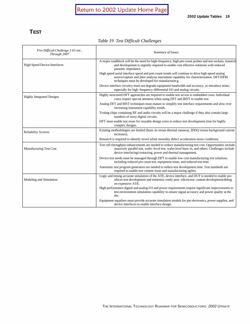
2002 Update Tables 19
THE INTERNATIONAL TECHNOLOGY ROADMAP FOR SEMICONDUCTORS: 2002 UPDATE
TEST Table 19 Test Difficult Challenges
Five Difficult Challenge ≥ 65 nm , Through 2007 Summary of Issues
High Speed Device Interfaces A major roadblock will be the need for high-frequency, high pin-count probes and test sockets; research
and development is urgently required to enable cost effective solutions with reduced parasitic impedance.
High speed serial interface speed and port count trends will continue to drive high speed analog
source/capture and jitter analysis instrument capability for characterization. DFT/DFM techniques must be developed for manufacturin g.
Device interface circuitry must not degrade equipment bandwidth and accuracy, or introduce noise; especially for high -frequency differential I/O and analog circuits.
Highly Integrated Designs Highly structured DFT approaches are required to enable test access to embedded cores. Individual cores require special attention when using DFT and BIST to enable test.
Analog DFT and BIST techniques must mature to simplify test interface requirements and slow ever increasing instrument capability trends.
Testing chips containing RF and audio circuits will be a major challenge if they also contain large numbers of noisy digital circuits.
DFT must enable test reuse for reusable design cores to reduce test development time for highly complex designs.
Reliability Screens Existing methodologies are limited (burn-in versus thermal runaway, IDDQ versus background current increases).
Research is required to identify novel infant mortality defect acceleration stress conditions
Manufacturing Test Cost Test cell throughput enhancements are needed to reduce manufacturing test cost. Opportunities include
massively parallel test, wafer-level test, wafer-level burn-in, and others. Challenges include device interfacing/contacting, power and thermal management.
Device test needs must be managed through DFT to enable low cost manufacturing test solutions; including reduced pin count test, equipment reuse, and reduced test time.
Automatic test program generators are needed to reduce test development time. Test standards are required to enable test content reuse and manufacturing agility.
Modeling and Simulation Logic and timing accurate simulation of the ATE, device interface, and DUT is needed to enable pre-
silicon test development and minimize costly post -silicon test content development/debug on expensive ATE.
High performance digital and analog I/O and power requirements require significant improvements to
test environment simulation capability to ensure signal accuracy and power quality at the die.
Equipment suppliers must provide accurate simulation models for pin electronics, power supplies, and device interfaces to enable interface design.

20 2002 Update Tables
THE INTERNATIONAL TECHNOLOGY ROADMAP FOR SEMICONDUCTORS: 2002 UPDATE
Table 19 Test Difficult Challenges (continued)
Five Difficult Challenges <65 nm, Beyond 2007 DUT to ATE interface Probing capability for optical and other disruptive technologies.
Support for massively parallel test - including full wafer contacting.
Decreasing die size and increasing circuit density are driving dramatic increases in die thermal density. This problem is further
magnified by the desire to enable parallel test to maximize manufacturing throughput. New thermal control techniques will be needed for wafer probe and component test.
DFT to enable test of device pins not contacted by the interface and test equipment.
Test Methodologies New DFT techniques (SCAN and BIST have been the mainstay for over 20 years). New test methods for control and observation are needed. Tests will need to be developed utilizing the design hierarchy.
Analog DFT and BIST techniques must mature to simplify test interface requirements and slow ever increasing instrument capability trends.
Logic BIST techniques must evolve to support new fault models, failure analysis, and deterministic test.
EDA tools for DFT insertion must support DFT selection with considerations for functionality, coverage, cost, circuit performance and ATPG performance.
Defect Analysis Defect types and behavior will continue to evolve with advances in fabrication process technology. Fundamental research in existing and novel fault models to address emerging defects will be required.
Significant advances in EDA tools for ATPG capacity and performance for advanced fault models and DFT insertion are required to improve efficiency and reduce design complexit ies associated with test.
Failure analysis. Realtime analysis of defects in multi-layer metal processes are needed.
Failure analysis methods analog devices must be developed and automated.
Transition from a destructive physical inspection process to a primarily non-destructive diagnostic capability. Characterization capabilities must identify, locate, and distinguish individual defect types.
Disruptive device technologies Develop new test methods for MEMS and sensors.
Develop new fault models for advanced/disruptive transistor structures.

2002 Update Tables 21
THE INTERNATIONAL TECHNOLOGY ROADMAP FOR SEMICONDUCTORS: 2002 UPDATE
Table 23a High Frequency Serial Communications Test Requirements—Near-term Year of Production 2001 2002 2003 2004 2005 2006 2007 DRAM ½ Pitch (nm) 130 115 100 90 80 70 65 MPU / ASIC ½ Pitch (nm) 150 130 107 90 80 70 65 MPU Printed Gate Length (nm) 90 75 65 53 45 40 35 MPU Physical Gate Length (nm) 65 53 45 37 32 28 25
High–performance-level serial transceivers
Serial data rate (Gbits/s) 10 10 40 40 40 40 40
Maximum reference clock speed (MHz) 667 667 2500 2500 2500 2500 2500
High-integration-level backplane and computer I/O
Serial data rate (Gbits/s) Production 2.5 3.125 3.125 10 10 40 40
Was Introduction 3.125 — 10 — 40 — —
Is Introduction 3.125 — 10 — 40 — —
Maximum port count at Production frequencies 20 100 200 100 200 100 200
at Introduction frequencies — — 20 — 20 — —
Maximum reference clock speed (MHz) Production 166 166 166 667 667 2500 2500
Introduction — — 667 — 2500 — —
White–Manufacturable Solutions Exist, and Are Being Optimized
Yellow–Manufacturable Solutions are Known
Red–Manufacturable Solutions are NOT Known

22 2002 Update Tables
THE INTERNATIONAL TECHNOLOGY ROADMAP FOR SEMICONDUCTORS: 2002 UPDATE
Table 28 DFT-BIST Device Test Requirements—Near-term** Year of Production 2001 2002 2003 2004 2005 2006 2007 Driver DRAM ½ Pitch (nm) 130 115 100 90 80 70 65 MPU / ASIC ½ Pitch (nm) 150 130 107 90 80 70 65 MPU Printed Gate Length (nm) 90 75 65 53 45 40 35 MPU Physical Gate Length (nm) 65 53 45 37 32 28 25
Number of parallel sites 32 32 64 64 128 128 128 Cost
Was Scan data volume(Giga-pin -vectors available per site) 6 6 12 12 16 16 16 Logic Density
Is Scan data volume(Giga-pin -vectors available per site) 6 6 12 12 16 16 32
Was Scan pin (available per site / system) 256/1K 256/1K 256/2K 256/2K 256/4K 256/4K 256/4K Logic Density
Is Scan pin (available per site / system) 256/1K 256/1K 384/2K 384/2K 512/4K 512/4K 512/4K
Scan vector rate (MT or MHz) 50 100 100 200 200 200 200 Test Time
“Full function” pin (available per site / system) 128/256128/256128/512 128/512 128/512 128/512 128/512 Test Time
Functional vector depth (M-Vectors) 16 16 16 16 16 16 16 Logic Density
Functional data rate (MHz) 100 100 100 200 200 200 200 Test Time
“Reduced function” pin (available per site / system)(DC only) 3K/4K 3K/4K 3K/4K 4K/5K 4K/5K 5K/6K 5K/6K I/O Density
Clock pins (available per site / system) 4/32 4/32 4/64 4/64 4/128 4/128 4/128 Clock Domains
Clock frequency (MHz) 200 200 400 400 400 800 800 On-chip Clock Rate
Power supplies (available per site / system) 8/32 8/32 8/64 8/64 8/128 8/128 8/128 Logic Density Support for options SoC
High-speed clock (differential pairs) yes yes yes yes yes yes yes
Signature compression yes yes yes yes yes yes yes
Algorithmic pattern generation yes yes yes yes yes yes yes
Low-frequency source and digitizer yes yes yes yes yes yes yes
High-frequency source and digitizer yes yes yes yes yes yes yes
Time measurement unit yes yes yes yes yes yes yes
ADC/DAC yes yes yes yes yes yes yes
RF source no no yes yes yes yes yes
High power yes yes yes yes yes yes yes
IDDQ yes yes yes yes yes yes yes
White–Manufacturable Solutions Exist, and Are Being Optimized
Yellow–Manufacturable Solutions are Known
Red–Manufacturable Solutions are NOT Known

2002 Update Tables 23
THE INTERNATIONAL TECHNOLOGY ROADMAP FOR SEMICONDUCTORS: 2002 UPDATE
Definitions for Table 28:
Parallel Sites—Parallel testing of devices is a common technique for reducing the effective cost of test per device by testing multiple devices with a single tester. The number of devices that can be tested in parallel will be necessarily limited by the tester’s available physical resources, however there should be no “logical” limit imposed by the hardware or software architecture. A common concern with these tables in the past has been the total number of pins that seem to be indicated by multiplying all of the numbers together, however this is not the intent. The total number of pins available on a given tester should be consistent with the current state-of-the-art for pin densities.
Scan Data Volume—The total number of bits shifted into the scan input pins plus the total number of bits shifted out of scan output pins. It is the total number of scan-able elements in a device multiplied by the total number of scan-loads plus the scan-unloads. A single bit shifted into a single device pin or shifted out of a single device pin can be defined as pin -vector (a tester architecture neutral unit).
Was Scan Pin —The maximum number of scan input pins and scan output pins. This number does not necessarily include the pins required for scan control.
Is Scan Pin —The maximum number of scan input pins plus scan output pins. This number does not necessarily include the pins required for scan control.
Scan Vector Rate—The maximum shift rate for scan data input pins and scan data output pins (expressed in MegaTransfers per second (MT)).
“Full Function” Pin —Full Function pins are backed by drive and receive resources containing the full functionality of a traditional ATE system pin. These resources may include, but are not necessarily limited to, precision timing accuracy, flexible waveform capability, high vector rates, programmable drive/receive thresholds, parametric measurement capability, etc. These “Full Function” pins are used to test the DUT via a traditional ATE approach utilizing device primary I/O pins which may include, but are not limited to the following functions: clock, input, output, bi-directional, and reference level bias (fixed state controlled by ATE pin electronics). In addition, the full function pins should be capable of scan (either within the limits of “Full Function” pin memory depth or with access to the scan memory).
Functional Vector Depth—The total number of vectors required to test a particular device. In this context, it refers to the total number of individual states (e.g., “0,” “1,” “H,” “L,” “X,” “Z,” etc.) applied to or received from a single device pin.
Functional Data Rate – The maximum rate of application of vectors to the data pins of the device.
“Reduced Function” Pin —Reduced Function pins are backed by low-cost resources containing limited digital drive/receive capability (e.g. static vectors are vectors that remain static for the duration of a particular test or subtest), no waveform capability, very little vector depth, etc. These pins will typically have programmable drive/receive thresholds, and parametric measurement capability.
Clock Pin —These single-ended clock pins function at higher frequencies and higher accuracies than the scan and functional data pins. These clocks are used for functional testing at the functional data rate, as well as, AC scan (shift slow – sample fast) and BIST, to facilitate high performance testing on DFT testers.
Clock Frequency—The maximum frequency attainable from the standard clock source. The accuracy and skew for the clock pins should be maintained to less than or equal to 8% of the minimum clock period and the jitter should be less than or equal to 1.5% of the minimum clock period.
Power Supplies—ATE device power supplies provide programmable voltage (or current) levels during testing. The most typical application is to apply voltage and current to a device’s primary power connections such as Vcc or Vdd. Other uses include reference voltage sources for device pins, termination voltages for external loads, and current sourcing during test. Device power supplies may be used in forcing either current or voltage while measuring the resulting voltage or current. Common feature include programmable clamps, measurement trigger/capture controlled by the tester’s pattern generator, and switch-able output voltage ranges controlled by the pattern generator. Supplies should be gang-able for flexibility.
Support for Options—There will always be a need to support options. This is driven by the need to support legacy devices in the Functional-to-Structural transition phase, as well as, for devices with mature DFT and some mixed-signal or extended performance requirements. The remaining line items in this table try to predict the need and performance requirements of some of the more typical of these options in the future. There are a number of analog options – these have been specifically identified, though this may not be a comprehensive list.
High-Speed Clock Pin —The high-speed clock pins function at higher frequencies and higher accuracies than the “standard” clock source. The high-speed clocks should support both single-ended operation and differential clock pairs. The maximum frequency required for this clock option is 800MHz through 2003, rising to 1.4GHz in 2004. The accuracy and skew for the high frequency clock pins should be maintained to less than or equal to 8% of the minimum clock period and the jitter should be less than or equal to 1.5% of the minimum clock period.

24 2002 Update Tables
THE INTERNATIONAL TECHNOLOGY ROADMAP FOR SEMICONDUCTORS: 2002 UPDATE
Definitions for Table 28 (continued):
Was
Signature Compression—Integrating Linear Feedback Shift Registers (LFSRs) with the scan channels on the DFT tester can dramatically reduce scan data volume and test time. Pseudo Random Pattern Generators (PRPGs) can be used to minimize the amount of scan-in stimuli that need to be stored in the scan buffer. Single Input Signature Registers (SISRs) can be used to compress scan-out measures. The PRPGs and SISRs should be integrated with the scan channels such that an individual scan cycle can interact with either its LFSR / SISR or scan channel. The LFSRs / SISRs should have programmable polynomials. The LFSRs/ SISRs should be capable of having their states seeded, reset, and observed under pattern op-code control and from states stored in pattern memory.
Is
Stimulus/Response Compression—Integrating Linear Feedback Shift Registers (LFSRs) as Pseudo Random Pattern Generators (PRPGs) or as Single Input Signature Registers (SISRs), on-chip, or with the scan channels on the DFT tester can dramatically reduce scan data volume and test time by minimizing the amount of test data that needs to be stored in the scan buffer. Single Input Signature Registers (SISRs) can be used to compress scan-out measures. The PRPGs and SISRs should be integrated with the scan channels such that an individual scan cycle can interact with either its LFSR / SISR or scan channel. The LFSRs / SISRs should have programmable polynomials. The LFSRs/ SISRs should be capable of having their states seeded, reset, and observed under pattern op-code control and from states stored in pattern memory.
Algorithmic Pattern Generation—Memory pattern sequences are generally repetitive and can, therefore, be generated algorithmically. Algorithmic Pattern Generator functionality should be integrated with other tester pattern sources to allow operation concurrently with stored stimulus/response test patterns.
Was Low Frequency Source/Digitizer—The ability to generate and digitize a differential analog waveform, such as a ramp or sine wave. Generally, 18-bit resolution up to 100KHz.
Is Low Frequency Source/Digitizer—The ability to generate and digitize a differential analog waveforms, such as a ramp or sine wave. Generally, 18-bit resolution up to 350K samples/second.
Was High Frequency Source/Digitizer—The ability to generate and digitize a differential analog waveform, such as a ramp or sine wave. Generally, 12-bit resolution up to 10MHz.
Is High Frequency Source/Digitizer—The ability to generate and digitize a differential analog waveform, such as a ramp or sine wave. Generally, 12-bit resolution up to 30M samples/second.
Was Time Measurement—Ability to measure a time interval or frequency.
Is Time Measurement—Ability to measure a time interval or frequency. The instrument should allow taking the measurement at the occurrence of an enabling event.
RF Source—As Radio Frequency functions find their way onto more and more SoCs and appropriate DFT sampling methodologies are developed for RF, there will be a need for external resources to generate clean, high frequency sine waves. The frequency requirements of these resource will be in the 100MHz to 6GHz range.
High Power—Some devices consume very high power (>75W), during tests. High-current device power supplies must deliv er accurate voltage and respond quickly to load changes (on the order of 1–2µs). In addition, significant current is applied through the tooling fixture and contactors or probe needles. There may be 1000s of device power pins in extremely tight physical density. The power supply must be capable of performing integrity tests that detect discontinuities such as power shorts to prevent damage to expensive test fixtures. In general, flexible user control of fast -acting safety/error, clamping, and shutdown hardware features becomes more important in high power delivery.
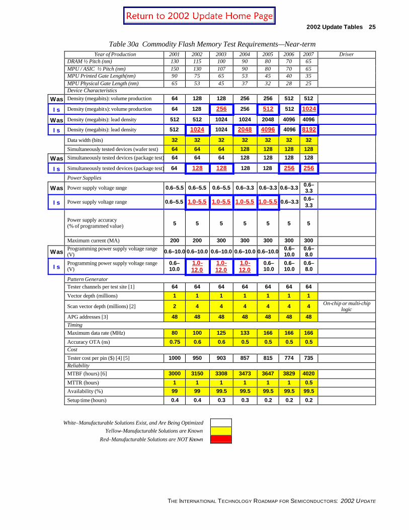
2002 Update Tables 25
THE INTERNATIONAL TECHNOLOGY ROADMAP FOR SEMICONDUCTORS: 2002 UPDATE
Table 30a Commodity Flash Memory Test Requirements—Near-term Year of Production 2001 2002 2003 2004 2005 2006 2007 Driver DRAM ½ Pitch (nm) 130 115 100 90 80 70 65 MPU / ASIC ½ Pitch (nm) 150 130 107 90 80 70 65 MPU Printed Gate Length(nm) 90 75 65 53 45 40 35 MPU Physical Gate Length (nm) 65 53 45 37 32 28 25 Device Characteristics
Was Density (megabits): volume production 64 128 128 256 256 512 512
Is Density (megabits): volume production 64 128 256 256 512 512 1024
Was Density (megabits): lead density 512 512 1024 1024 2048 4096 4096
Is Density (megabits): lead density 512 1024 1024 2048 4096 4096 8192
Data width (bits) 32 32 32 32 32 32 32 Simultaneously tested devices (wafer test) 64 64 64 128 128 128 128
Was Simultaneously tested devices (package test) 64 64 64 128 128 128 128
Is Simultaneously tested devices (package test) 64 128 128 128 128 256 256 Power Supplies
Was Power supply voltage range 0.6–5.5 0.6–5.5 0.6–5.5 0.6–3.3 0.6–3.3 0.6–3.3 0.6–3.3
Is Power supply voltage range 0.6–5.5 1.0-5.5 1.0-5.5 1.0-5.5 1.0-5.5 0.6–3.3 0.6–3.3
Power supply accuracy (% of programmed value) 5 5 5 5 5 5 5
Maximum current (MA) 200 200 300 300 300 300 300
Was Programming power supply voltage range (V) 0.6–10.0 0.6–10.0 0.6–10.0 0.6–10.0 0.6–10.0 0.6–
10.0 0.6–8.0
Is Programming power supply voltage range (V)
0.6–10.0
1.0-12.0
1.0-12.0
1.0-12.0
0.6–10.0
0.6–10.0
0.6–8.0
Pattern Generator
Tester channels per test site [1] 64 64 64 64 64 64 64 Vector depth (millions) 1 1 1 1 1 1 1
Scan vector depth (millions) [2] 2 4 4 4 4 4 4 On-chip or multi-chip logic
APG addresses [3] 48 48 48 48 48 48 48 Timing
Maximum data rate (MHz) 80 100 125 133 166 166 166 Accuracy OTA (ns) 0.75 0.6 0.6 0.5 0.5 0.5 0.5 Cost
Tester cost per pin ($) [4] [5] 1000 950 903 857 815 774 735 Reliability
MTBF (hours) [6] 3000 3150 3308 3473 3647 3829 4020 MTTR (hours) 1 1 1 1 1 1 0.5 Availability (%) 99 99 99.5 99.5 99.5 99.5 99.5 Setup time (hours) 0.4 0.4 0.3 0.3 0.2 0.2 0.2
White–Manufacturable Solutions Exist, and Are Being Optimized Yellow–Manufacturable Solutions are Known
Red–Manufacturable Solutions are NOT Known

26 2002 Update Tables
THE INTERNATIONAL TECHNOLOGY ROADMAP FOR SEMICONDUCTORS: 2002 UPDATE
Table 30b Commodity Flash Memory Test Requirements—Long-term Year of Production 2010 2013 2016 Driver DRAM ½ Pitch (nm) 45 32 22 MPU / ASIC ½ Pitch (nm) 45 32 22 MPU Printed Gate Length (nm) 25 18 13 MPU Physical Gate Length (nm) 18 13 9 Device Characteristics
Density (megabits): volume production 2048 4096 8192
Density (megabits): lead density 16384 65536 131072
Data width (bits) 32 32 32
Was Simultaneously tested devices (wafer test) 256 256 256
Is Simultaneously tested devices (wafer test) 256 512 512
Simultaneously tested devices (package test) 256 256 256 Power Supplies
Power supply voltage range 0.6–3.30.6–3.3 0.6–3.3
Power supply accuracy (% of programmed value) 5 5 5
Maximum current (MA) 300 300 300
Programming power supply voltage range (V) 0.6–8.00.6–8.0 0.6–8.0
Pattern Generator
Tester channels per test site [1] 72 72 72
Vector depth (millions) 2 2 2
Scan vector depth (millions) [2] 8 8 8 On-chip or multi-chip logic
APG addresses [3] 48 48 48
Timing
Maximum data rate (MHz) 200 250 300
Accuracy OTA (ns) 0.3 0.2 0.1
Cost
Tester cost per pin ($) [4] [5] 630 540 463
Reliability
MTBF (hours) [6] 4654 5388 6237
MTTR (hours) 0.5 0.5 0.5
Availability (%) 99.5 99.5 99.5
Setup time (hours) 0.2 0.2 0.2
White–Manufacturable Solutions Exist, and Are Being Optimized Yellow–Manufacturable Solutions are Known
Red–Manufacturable Solutions are NOT Known

2002 Update Tables 27
THE INTERNATIONAL TECHNOLOGY ROADMAP FOR SEMICONDUCTORS: 2002 UPDATE
Table 32a Burn-in Requirements—Near-term Year of Production 2001 2002 2003 2004 2005 2006 2007 DRAM ½ Pitch (nm) 130 115 100 90 80 70 65 MPU / ASIC ½ Pitch (nm) 150 130 107 90 80 70 65 MPU Printed Gate Length (nm) 90 75 65 53 45 40 35 MPU Physical Gate Length (nm) 65 53 45 37 32 28 25 High Performance ASIC
Clock input frequency (MHz) 400 400 400 400 400 400 400 Off-chip data frequency (MHz) 25 50 50 75 75 75 75 Power supply voltage range (V) 0.7–4.0 0.7–4.0 0.7–3.3 0.7–2.5 0.5–2.5 0.5–2.5 0.5–2.5
Was Power dissipation (W per DUT) 130 140 150 150 200 200 200
Is Power dissipation (W per DUT) 30 40 50 75 100 150 200
Maximum number of signal I/O 384 384 384 384 384 384 384 High Performance Microprocessor
Was Clock input frequency (MHz) 150 200 200 250 250 250 250
Is Clock input frequency (MHz) 150 200 200 250 400 400 400
Off-chip data frequency (MHz) 33 75 75 75 75 75 75 Was Power supply voltage range (V) 0.7–4.0 0.7–3.5 0.7–3.5 0.5–3.5 0.5–3.5 0.5–3.5 0.5–3.5
Is Power supply voltage range (V) 0.7–4.0 0.7–3.5 0.7–3.5 0.5–3.5 0.5–2.5 0.5–2.5 0.5–2.5Was Power dissipation (W per DUT) 150 200 200 250 300 300 300
Is Power dissipation (W per DUT) 150 200 200 250 600 600 600
Was Maximum current (A) 75 150 150 300 300 300 300
Is Maximum current (A) 75 150 150 300 400 450 450
Maximum number of signal I/O 128 128 128 128 128 128 128 Low-End Microcontroller Clock frequency (MHz) 25 100 200 300 400 400 400 Off-chip data frequency (MHz) 25 40 50 60 75 75 75 Power supply voltage range (V) 0.7–12.00.7–12.00.7–12.00.7–10.00.7–10.0 0.7–10.0 0.7–10.0 Power dissipation (W per DUT) 3 5 5 10 10 10 10 Maximum number of signal I/O 32 32 32 32 32 32 32 Mixed-Signal Clock input frequency (MHz) 150 200 200 250 250 250 250 Off-chip data frequency (MHz) 33 75 75 75 75 75 75 Power supply voltage range (V) 0.7–65.00.7–65.00.7–100 0.7–100 0.5–500 0.5–500 0.5–500 Power dissipation (W per DUT) 50 50 75 75 150 150 150 Maximum current (A) 20 20 20 20 20 20 20 Maximum number of signal I/O 128 128 128 128 128 128 128 Analog signal peak-to-peak voltage range (V) ±10V ±10V ±10V ±10V ±10V ±10V ±10V Commodity Memory
Clock input frequency (MHz) 400 400 400 400 400 400 400 Off-chip data frequency (MHz) 30 30 30 50 50 50 50 Power supply voltage range (V) 0.6–6.0 0.6–6.0 0.6–6.0 0.6–4.0 0.6–4.0 0.6–4.0 0.6–4.0 Programming power supply voltage range (V) 0.6–10 0.6–10 0.6–10 0.6–10 0.6–10 0.6–10 0.6–8 Power dissipation (W per DUT) 2 5 10 15 20 20 20 Maximum number of signal I/O 18 36 36 72 72 72 72 DFT / BIST Requirements Scan pin count (per DUT) 128 128 128 128 128 128 128 Scan vector memory depth (megavectors) 64 128 256 256 256 256 256 Scan vector frequency (MHz) 33 75 75 75 75 75 75
White–Manufacturable Solutions Exist, and Are Being Optimized
Yellow–Manufacturable Solutions are Known
Red–Manufacturable Solutions are NOT Known

28 2002 Update Tables
THE INTERNATIONAL TECHNOLOGY ROADMAP FOR SEMICONDUCTORS: 2002 UPDATE
Table 32b Burn-in Requirements—Long-term Year of Production 2010 2013 2016 DRAM ½ Pitch (nm) 45 32 22 MPU / ASIC ½ Pitch (nm) 45 32 22 MPU Printed Gate Length (nm) 25 18 13 MPU Physical Gate Length (nm) 18 13 9 High Performance ASIC Clock input frequency (MHz) 400 400 400 Off-chip data frequency (MHz) 75 75 75 Power supply voltage range (V) 0.5–2.5 0.5–2.5 0.4–2.5 Power dissipation (W per DUT) 200 225 250 Maximum number of signal I/O 384 384 384 High Performance Microprocessor
Was Clock input frequency (MHz) 250 250 250
Is Clock input frequency (MHz) 400 400 400
Off-chip data frequency (MHz) 75 75 75 Was Power supply voltage range (V) 0.5–3.0 0.5–2.5 0.5–2.5
Is Power supply voltage range (V) 0.5–2.5 0.5–2.5 0.5–2.5
Was Power dissipation (W per DUT) 300 300 300
Is Power dissipation (W per DUT) 600 600 600
Was Maximum current (A) 300 300 300
Is Maximum current (A) 450 450 450
Maximum number of signal I/O 128 128 128 Low-End Microcontroller Clock frequency (MHz) 400 400 400 Off-chip data frequency (MHz) 75 75 75 Power supply voltage range (V) 0.5–10 0.5–10 0.5–10 Power dissipation (W per DUT) 20 20 20 Maximum number of signal I/O 32 32 32 Mixed-Signal Clock input frequency (MHz) 250 250 250 Off-chip data frequency (MHz) 75 75 75 Power supply voltage range (V) 0.5–500 0.5–1000 0.5–1000 Power dissipation (W per DUT) 150 150 150 Maximum current (A) 30 30 30 Maximum number of signal I/O 128 128 128 Analog signal peak-to-peak voltage range (V) ±10V ±10V ±10V Commodity Memory Clock input frequency (MHz) 400 400 400 Off-chip data frequency (MHz) 50 50 50 Power supply voltage range (V) 0.5–4.0 0.5–4.0 0.5–4.0 Programming power supply voltage range (V) 0.5–8.0 0.5–8.0 0.5–8.0 Power dissipation (W per DUT) 20 20 20 Maximum number of signal I/O 72 72 72 DFT / BIST Requirements Scan pin count (per DUT) 128 128 128 Scan vector memory depth (megavectors) 256 256 256 Scan vector frequency (MHz) 75 75 75
White–Manufacturable Solutions Exist, and Are Being Optimized
Yellow–Manufacturable Solutions are Known
Red–Manufacturable Solutions are NOT Known

2002 Update Tables 29
THE INTERNATIONAL TECHNOLOGY ROADMAP FOR SEMICONDUCTORS: 2002 UPDATE
PROCESS INTEGRATION, DEVICES, AND STRUCTURES Table 34 Process Integration Difficult Challenges [Update]
Difficult Challenges ≥ 65nm / Through 2007 Summary of Issues
Was 1. High-performance applications: meeting performance and power dissipation requirements for highly scaled MOSFETs.
– Cost effectiveness, process control, and reliability of very thin oxy-nitride gate dielectrics, especially considering the high gate leakage. – Implementation of metal gate electrode by about 2007. – Need to reduce series S/D parasitic resistance. – Controlling static power dissipation in the face of rapidly increasing leakage. – Architecture and circuit design improvement and innovation will be needed
Is 1. High-performance applications: meeting performance and power dissipation requirements for highly scaled MOSFETs.
– Cost effectiveness, process control, and reliability of very thin oxy-nitride gate dielectrics, especially considering the high gate leakage. – Implementation of metal gate electrode and high κ gate dielectric by about 2007. – Need to reduce series S/D parasitic resistance. – Controlling st atic power dissipation in the face of rapidly increasing leakage. – Architecture and circuit design improvement and innovation will be needed
2. Low-power applications: meeting performance and leakage requirements for highly scaled MOSFETs.
– Early availability of manufacturing-worthy high κ gate dielectrics is necessary to meet stringent gate leakage and performance requirements. – Very slow scaling of Vdd will make overall device scaling difficult.
3. Implementation into manufacturing of non-classical MOSFET devices (for example, double-gate SOI).
– It is likely that these transistors will be necessary eventually to control short -channel and other effects in highly scaled devices. See Emerging Research Devices section, Non-classical CMOS, for more detail.
4. Ensuring reliability of new materials and structures in a timely manner.
– Accelerated reliability ensurance of high κ material for gate stack will be needed for early insertion into manufacturing. – Ensuring reliability of new gate electrode materials will be a challenge. – Ensuring reliability of new, non-classical CMOS structures will be a challenge. – Ensuring reliability of very thin oxy-nitrides with very high leakage current will be critical for high -performance applications. – Difficulty of screening with high leakage currents
5. Constructing DRAM, SRAM, and high density nonvolatile memory (NVM) for scaled technologies
– DRAM main issues: adequate storage capacitance for devices with reduced feature size; access device design; holding the overall leakage to acceptably low levels; and deploying low sheet resistance materials for bit and word lines to ensure desired speed for scaled DRAMs. Also, the availability of manufacturing worthy 193 nm lithography and integrated DRAM etch capability for 100 nm half pitches in 2003. – SRAM: difficult lithography and etch as well as process integration issues. – NVM: very difficult scaling issues with tunnel and interpoly dielectrics.
6. High-performance mixed-signal solutions for scaled technologies.
– Passive element scaling: embedded inductor densities and Q factor values. – Signal isolation. – Optimizing RF CMOS devices with scaled technologies: gate leakage is a particularly sensitive issue. – Transition to reduced analog supply voltages. – Difficulty and cost of integrating analog/RF and high -performance digital functions on a chip.

30 2002 Update Tables
THE INTERNATIONAL TECHNOLOGY ROADMAP FOR SEMICONDUCTORS: 2002 UPDATE
Table 34 Process Integration Difficult Challenges [Update](continued)
Difficult Challenges < 65 nm, Beyond 2007 Summary of Issues
7. Fundamental improvements in MOSFET device effective transconductance needed to maintain device performance scaling trend.
– With sharp reductions in Vdd and 17% annual increase in intrinsic transistor speed, basic MOSFET device performance will be inadequate to meet circuit speed requirements.
8. Dealing with atomic-level fluctuations and statistical process variations in sub-30 nm MOSFETs.
– Fundamental problems of atomic-level statistical fluctuations are not completely understood.
9. New interconnect schemes – Eventually, copper/low κ performances will be inadequate. – Solutions (optical, microwave/RF, etc,) are currently unclear.
10 Toward the end of the Roadmap or beyond, implementation of advanced non-CMOS devices and architectures, including memory.
– Will drive major changes in process, materials, physics, design, etc. – Non-CMOS devices may coexist with CMOS: integration of the two will be difficult, especially for mixed signal. – See Emerging Research Devices sections for more discussion and detail.
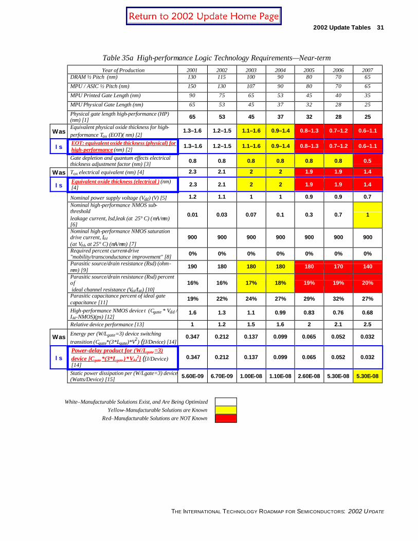
2002 Update Tables 31
THE INTERNATIONAL TECHNOLOGY ROADMAP FOR SEMICONDUCTORS: 2002 UPDATE
Table 35a High-performance Logic Technology Requirements—Near-term Year of Production 2001 2002 2003 2004 2005 2006 2007 DRAM ½ Pitch (nm) 130 115 100 90 80 70 65
MPU / ASIC ½ Pitch (nm) 150 130 107 90 80 70 65
MPU Printed Gate Length (nm) 90 75 65 53 45 40 35
MPU Physical Gate Length (nm) 65 53 45 37 32 28 25
Physical gate length high-performance (HP) (nm) [1] 65 53 45 37 32 28 25
Was Equivalent physical oxide thickness for high-performance Tox (EOT)( nm) [2]
1.3–1.6 1.2–1.5 1.1–1.6 0.9–1.4 0.8–1.3 0.7–1.2 0.6–1.1
Is EOT: equivalent oxide thickness (physical) for high-performance (nm) [2]
1.3–1.6 1.2–1.5 1.1–1.6 0.9–1.4 0.8–1.3 0.7–1.2 0.6–1.1
Gate depletion and quantum effects electrical thickness adjustment factor (nm) [3] 0.8 0.8 0.8 0.8 0.8 0.8 0.5
Was Tox electrical equivalent (nm) [4] 2.3 2.1 2 2 1.9 1.9 1.4
Is Equivalent oxide thickness (electrical ) (nm) [4] 2.3 2.1 2 2 1.9 1.9 1.4
Nominal power supply voltage (Vdd) (V) [5] 1.2 1.1 1 1 0.9 0.9 0.7
Nominal high-performance NMOS sub-threshold leakage current, Isd,leak (at 25° C) (µA/µm) [6]
0.01 0.03 0.07 0.1 0.3 0.7 1
Nominal high-performance NMOS saturation drive current, Idd
(at Vdd, at 25° C) (µA/µm) [7] 900 900 900 900 900 900 900
Required percent current-drive "mobility/transconductance improvement" [8] 0% 0% 0% 0% 0% 0% 0%
Parasitic source/drain resistance (Rsd) (ohm-µm) [9]
190 180 180 180 180 170 140
Parasitic source/drain resistance (Rsd) percent of ideal channel resistance (Vdd/Idd) [10]
16% 16% 17% 18% 19% 19% 20%
Parasitic capacitance percent of ideal gate capacitance [11]
19% 22% 24% 27% 29% 32% 27%
High-performance NMOS device τ (Cgate * Vdd / Idd-NMOS)(ps) [12]
1.6 1.3 1.1 0.99 0.83 0.76 0.68
Relative device performance [13] 1 1.2 1.5 1.6 2 2.1 2.5
Was Energy per (W/Lgate=3) device switching transition (Cgate*(3*Lgate)*V2) (fJ/Device) [14]
0.347 0.212 0.137 0.099 0.065 0.052 0.032
Is Power-delay product for (W/L gate=3) device [C gate*(3*L gate)*V dd
2] (fJ/Device) [14]
0.347 0.212 0.137 0.099 0.065 0.052 0.032
Static power dissipation per (W/Lgate=3) device (Watts/Device) [15] 5.60E-09 6.70E-09 1.00E-08 1.10E-08 2.60E-08 5.30E-08 5.30E-08
White–Manufacturable Solutions Exist, and Are Being Optimized Yellow–Manufacturable Solutions are Known
Red–Manufacturable Solutions are NOT Known

32 2002 Update Tables
THE INTERNATIONAL TECHNOLOGY ROADMAP FOR SEMICONDUCTORS: 2002 UPDATE
Table 35b High-performance Logic Technology Requirements—Long-term
Year of Production 2010 2013 2016
DRAM ½ Pitch (nm) 45 32 22
MPU / ASIC ½ Pitch (nm) 50 35 25
MPU Printed Gate Length (nm) 25 18 13
MPU Physical Gate Length (nm) 18 13 9
Physical gate length high-performance (HP) (nm) [1] 18 13 9
Was Equivalent physical oxide thickness for high-performance Tox (EOT) ( nm) [2] 0.5-0.8 0.4-0.6 0.4-0.5
Is EOT: equivalent oxide thickness (physical) for high-performance (nm) [2] 0.5-0.8 0.4-0.6 0.4-0.5
Gate depletion and quantum effects electrical thickness adjustment factor (nm) [3] 0.5 0.5 0.5
Was Tox electrical equivalent (nm) [4] 1.2 1 0.9
Is Equivalent oxide thickness (electrical ) (nm) [4] 1.2 1 0.9
Nominal power supply voltage (Vdd) (V) [5] 0.6 0.5 0.4
Nominal high-performance NMOS sub threshold leakage current, Isd,leak (at 25° C) (µA/µm) [6] 3 7 10
Nominal high-performance NMOS saturation drive current , Idd (at Vdd, at 25° C) (µA/µm) [7]
1200 1500 1500
Required percent current-drive "mobility/transconductance improvement" [8] 30% 70% 100%
Parasitic source/drain resista nce (Rsd) (ohm-µm) [9] 110 90 80
Parasitic source/drain resistance (Rsd) percent of ideal channel resistance (Vdd/Idd) [10] 25% 30% 35%
Parasitic capacitance percent of ideal gate capacitance [11] 31% 36% 42%
High-performance NMOS device τ (Cgate * Vdd / Idd-NMOS)(ps) [12] 0.39 0.22 0.15
Relative device performance [13] 4.3 7.2 10.7
Was Energy per (W/Lgate=3) device switching transition (Cgate*(3*Lgate)*V2) (fJ/Device) [14] 0.015 0.007 0.002
Is Power-delay product for (W/L gate=3) device [C gate*(3*L gate)*V dd2] (fJ/Device) [14] 0.015 0.007 0.002
Static power dissipation per (W/Lgate=3) device (Watts/Device) [15] 9.70E-08 1.40E-07 1.10E-07
White–Manufacturable Solutions Exist, and Are Being Optimized Yellow–Manufacturable Solutions are Known
Red–Manufacturable Solutions are NOT Known

2002 Update Tables 33
THE INTERNATIONAL TECHNOLOGY ROADMAP FOR SEMICONDUCTORS: 2002 UPDATE
Notes for Table 35a and b:
[1] Values set by ORTC. Gate dimensional control is set by the Lithography and FEP Etch ITWGs, and is assumed to have a three sigma value of ± 10%. Gate dimension variation is assumed to be the primary factor responsible for driving device parameter variation.
Was [2] EOT range set by FEP TWG. Yellow/red feasibility coloring set by FEP TWG projections on thickness control and reliability capability. Calculations in rest of PIDS table (and the underlying PIDS workbook) based on approximate midpoint EOT values.
Is
[2] EOT range set by FEP TWG. Yellow/red feasibility coloring set by FEP TWG projections on thickness control and reliability capability. Calculations in rest of PIDS table (and the underlying PIDS workbook) based on approximate midpoint EOT values. For a gate dielectric of thickness T d and relative dielectric constant k, EOT is defined by: EOT = Td / (k/3.9), where 3.9 is the relative dielectric constant of thermal silicon dioxide. The ideal gate capacitance per unit area of the gate dielectric of thickness Td is the same as that of a gate dielectric made up of thermal silicon dioxide with a thickness of EOT.
[3] Accounts for gate electrode depletion and inversion-layer quantum effects. Yellow feasibility coloring reflects FEP assessment of polysilicon doping capability; red feasibility coloring reflects the introduction of metal-gate electrodes by 2007 (which reduces the gate depletion value).
[4] Sum of midpoint EOT and Electrical Thickness Adjustment Factor. Used in CV/I performance metric and CV2 dynamic power metric calculations. Red/yellow feasibility coloring determined by worst-case EOT and Electrical Thickness Adjustment Factor red/yellow feasibility coloring.
Was [5] Nominal power supply voltage has been set to maintain sufficient voltage over-drive to continue historical approximate 17% per year device performance scaling while still enabling approximate 30% per year switching energy reduction and still maintaining reasonable vertical gate dielectric electric field strengths. Actual power supply voltage values may vary +/- 10%, depending on the particular circuit design application or technology optimization.
Is
[5] Nominal power supply voltage has been set to maintain sufficient voltage over-drive to continue historical approximate 17% per year device performance scaling while still enabling approximate 30% per year switching energy reduction and still maintaining reasonable vertical gate dielectric electric field strengths. Actual target power supply voltage values may vary +/- 10%, depending on the particular circuit design application or technology optimization.
[6] Nominal sub-threshold leakage current is defined as the NMOSFET source current at room temperature with the drain bias set equal to the nominal power-supply voltage and with the gate, source and substrate biases set to zero volts; all MOSFET device dimensions are assumed to be at their nominal/target values. Total NMOS off-state current is the NMOSFET drain current at room temperature, and is the sum of the NMOS sub-threshold, gate, and junction leakage current components. The sub-threshold leakage current is assumed to be larger than either the gate or junction leakage current components at either room or high-temperature conditions. The threshold voltage value (and the corresponding sub-threshold current) has been set to maintain sufficient voltage over-drive to continue historical approximate 17% per year device performance scaling. Yellow feasibility coloring by 2007 reflects the potential need for non-classical CMOS or ultra -shallow junction technology in order to control short-channel and/or high-field effects (See Emerging Research Devices section). The above sub-threshold, gate, and junction current scaling scenario also applies to PMOS devices. Note, sub-threshold current value applies to fastest MOS devices only; slower/lower-leakage MOS devices will also be available. Future systems will consist of a mix of both high and lower-leakage devices.
[7] Nominal saturation current drive is defined as the MOSFET drain current at room temperature with the gate bias and the drain bias set equal to the nominal power-supply voltage; all MOSFET device dimensions are assumed to be at their nominal/target values. Nominal PMOS saturation current-drive value is assumed to be 40-50% of the nominal NMOS saturation current-drive value. Yellow/red feasibility coloring indicates the projected need for fundamental device current-drive (or transconductance/mobility) improvement by 2010 in order to continue historical approximate 17% per year device performance scaling. NMOS/PMOS current-drive targets are approximate with only 1.5 significant digits of accuracy.
[8] Fundamental device mobility/transconductance improvement needed by 2010 in order to continue historical approximate 17% per year device performance scaling. Yellow/red feasibility coloring indicates the difficulty in implementing fundamental device current-drive (transconductance/mobility) improvement required in 2010 and later to continue historical approximate 17% per year device performance scaling.
Was [9] Total parasitic device source/drain resistance Rsd (sum of the source and drain parasitic resistances). Rsd targets are consistent with FEP TWG projections. Yellow/red feasibility coloring reflects FEP TWG projections on contact resistance, salicide sheet resistance, and drain extension scaling. Similar Rsd values are assumed for the LOP and LSTP devices.
Is [9] Maximum allowable parasitic device source/drain resistance Rsd (sum of the source and drain parasitic resistances). Rsd targets are consistent with FEP TWG projections. Yellow/red feasibility coloring reflects FEP TWG projections on contact resistance, salicide sheet resistance, and drain extension scaling. Similar Rsd values are assumed for the LOP and LSTP devices.
Was [10] Maximum ratio of the parasitic device source/drain resistance (Rsd) to the ideal channel resistance (Vdd/Idd). Rsd targets are consistent with FEP TWG projections. Yellow/red feasibility coloring reflects FEP TWG projections on contact resistance, salicide sheet resistance, and drain extension scaling.
Is 10] Maximum Ratio of the parasitic device source/drain resistance (Rsd) to the ideal channel resistance (Vdd/Idd). Rsd targets are consistent with FEP TWG projections. Yellow/red feasibility coloring reflects FEP TWG projections on contact resistance, salicide sheet resistance, and drain extension scaling.

34 2002 Update Tables
THE INTERNATIONAL TECHNOLOGY ROADMAP FOR SEMICONDUCTORS: 2002 UPDATE
Notes for Table 35a and b(continued)
Was
[11] Maximum ratio of the parasitic gate overlap/fringing capacitance to the ideal gate capacitance. Assume constant C-parasitic value of 2.4E-16F/um. [3 × the fringing capacitance value per side, including the Miller effect]; this value is assumed to be independent of bias conditions and/or technology. Parasitic capacitance factor is included in CV/I and CV2 performance and power metric calculations. Similar parasitic capacitance values are assumed for the LOP and LSTP devices.
Is 11] Maximum ratio of the parasitic gate overlap/fringing capacitance to the ideal gate capacitance. Assume constant C-parasitic value of 2.4E-16F/um. [3 × the fringing capacitance value per side, including the Miller effect]; this value is assumed to be independent of bias conditions and/or technology. Parasitic capacitance factor is included in CV/I and CV2 performance and power metric calculations. Similar parasitic capacitance values are assumed for the LOP and LSTP devices.
[12] τ = CV/I intrinsic delay metric for NMOS device; PMOS CV/I metric assumed to scale proportionally. The CV/I metric provides an indication of the intrinsic switching delay of the device, while 1/τ, the reciprocal of CV/I, is a good metric for the intrinsic switching speed of the device. Red/yellow feasibility coloring determined by worst-case saturation current-drive feasibility coloring.
[13] Improvement in 1/τ NMOS performance metric normalized to the year 2001. Maintains historical approximate 17% per year device performance improvement scaling trend. Red/yellow feasibility coloring determined by worst-case, saturation current-drive feasibility coloring.
Was [14] CV2switching energy metric for an NMOS device with dimensions W/Lgate=3. The switching energy metric indicates the amount of dynamic power required to switch the device. Maintains approximate 30% per year device switching energy reduction scaling trend. Red/yellow feasibility coloring determined by worst-case saturation current-drive feasibility and mobility/transconductance improvement feasibility coloring.
Is 14] CV2switching energy metric for an NMOS device with dimensions W/Lgate=3 . The power-delay product indicates the amount of dynamic energy required to switch the device through a full (up and down) transition. Maintains approximate 30% per year device switching energy reduction scaling trend. Red/yellow feasibility coloring determined by worst-case saturation current-drive feasibility and mobility/transconductance improvement feasibility coloring.
[15] Static power dissipation for an NMOS device with dimensions W/Lgate=3. Assume that the device static power is primarily determined by the sub-threshold current (since the other junction and leakage current components are assumed to be lower). Yellow feasibility coloring by 2007 reflects the potential need for non-classical CMOS or ultra -shallow junction technology in order to control short-channel and/or high-field effects (See Emerging Research Devices section, Non-classical CMOS).

2002 Update Tables 35
THE INTERNATIONAL TECHNOLOGY ROADMAP FOR SEMICONDUCTORS: 2002 UPDATE
Table 36a Low Operating Power (LOP) Logic Technology Requirements—Near-term Year of Production 2001 2002 2003 2004 2005 2006 2007
DRAM ½ Pitch (nm) 130 115 100 90 80 70 65
MPU / ASIC ½ Pitch (nm) 150 130 107 90 80 70 65
MPU Printed Gate Length (nm) 90 75 65 53 45 40 35
MPU Physical Gate Length (nm) 65 53 45 37 32 28 25
Physical gate length low-operating power (LOP) (nm) [1] 90 75 65 53 45 37 32
Was Equivalent physical oxide thickness for LOP Tox (EOT) (nm) [2] 2.0-2.4 1.8-2.2 1.6-2.0 1.4-1.8 1.2-1.6 1.1-1.5 1.0-1.4
Is EOT: equivalent oxide thickness (physical) for LOP (nm) [2] 2.0-2.4 1.8-2.2 1.6-2.0 1.4-1.8 1.2-1.6 1.1-1.5 1.0-1.4
Electrical thickness adjustment factor (gate depletion and quantum effects) (nm) [3] 0.8 0.8 0.8 0.8 0.8 0.8 0.5
Was Tox electrical equivalent (nm) [4] 3 2.8 2.6 2.4 2.2 2.1 1.7
Is Equivalent oxide thickness (electrical ) (nm) [4] 3 2.8 2.6 2.4 2.2 2.1 1.7
Nominal LOP power supply voltage (Vdd) (V) [5] 1.2 1.2 1.1 1.1 1 1 0.9
Nominal LOP NMOS sub-threshold leakage current, Isd,leak (@25C) (pA/µm) [6]
100 100 100 300 300 300 700
Nominal LOP NMOS Saturation drive current, Idd (@Vdd, @25C) (µA/µm) [7]
600 600 600 600 600 600 700
Required percent current-drive "mobility/transconductance improvement" [8] 0% 0% 0% 0% 0% 0% 0%
LOP NMOS Device τ (Cgate * Vdd / Id-NMOS) (ps) [9] 2.55 2.45 2.02 1.84 1.58 1.41 1.14
LOP relative device performance [10] 1 1.04 1.3 1.4 1.6 1.8 2.2
Was Energy per (W/Lgate=3) device switching transition (Cgate*(3*Lgate)*V2) (fJ/Device) [11]
0.496 0.424 0.26 0.193 0.128 0.094 0.069
Is Power-delay product for (W/L gate=3) device [C gate*(3*L gate)*V dd
2] (fJ/Device) [14] 0.496 0.424 0.26 0.193 0.128 0.094 0.069
Static power dissipation per (W/Lgate=3) device (Watts/device) [12] 3.20E-11 2.90E-11 2.10E-11 5.20E-11 4.10E-11 3.30E-11 6.00E-11
White–Manufacturable Solutions Exist, and Are Being Optimized Yellow–Manufacturable Solutions are Known
Red–Manufacturable Solutions are NOT Known

36 2002 Update Tables
THE INTERNATIONAL TECHNOLOGY ROADMAP FOR SEMICONDUCTORS: 2002 UPDATE
Table 36b Low Operating Power (LOP) Logic Technology Requirements—Long-term
Year of Production 2010 2013 2016
DRAM ½ Pitch (nm) 45 32 22
MPU / ASIC ½ Pitch (nm) 50 35 25
MPU Printed Gate Length (nm) 25 18 13
MPU Physical Gate Length (nm) 18 13 9
Physical gate length low-operating power (LOP) (nm) [1] 22 16 11
Was Equivalent physical oxide thickness for LOP Tox (EOT) (nm) [2] 0.8-1.2 0.7-1.1 0.6-1.0
Is EOT: equivalent oxide thickness (physical) for high-performance (nm) [2] 0.8-1.2 0.7-1.1 0.6-1.0
Electrical thickness adjustment factor (gate depletion and quantum effects) (nm) [3] 0.5 0.5 0.5
Was Tox electrical equivalent (nm) [4] 1.5 1.4 1.3
Is Equivalent oxide thickness (electrical ) (nm) [4] 1.5 1.4 1.3
Nominal LOP power supply voltage (Vdd) (V) [5] 0.8 0.7 0.6
Nominal LOP NMOS sub-threshold leakage current, Isd,leak (@25C) (pA/µm) [6] 1000 3000 10000
Nominal LOP NMOS saturation drive current, Idd (@Vdd, @25C) (µA/µm) [7] 700 800 900
Required percent current-drive "mobility/transconductance improvement" [8] 10% 30% 70%
LOP NMOS device τ (Cgate * Vdd / Idd-NMOS) (ps) [9] 0.85 0.56 0.35
LOP relative device Performance [10] 3 4.6 7.2
Was Energy per (W/Lgate=3) device switching transition (Cgate*(3*Lgate)*V2) (fJ/Device) [11] 0.032 0.015 0.006
Is Power-delay product for (W/L gate=3) device [C gate*(3*L gate)*V dd2] (fJ/Device)
[14] 0.032 0.015 0.006
Static power dissipation per (W/Lgate=3) device (Watts/Device) [12] 5.30E-11 1.00E-10 2.00E-10
White–Manufacturable Solutions Exist, and Are Being Optimized Yellow–Manufacturable Solutions are Known
Red–Manufacturable Solutions are NOT Known

2002 Update Tables 37
THE INTERNATIONAL TECHNOLOGY ROADMAP FOR SEMICONDUCTORS: 2002 UPDATE
Table 36c Low Standby Power (LSTP) Technology Requirements—Near-term Year of Production 2001 2002 2003 2004 2005 2006 2007
DRAM ½ Pitch (nm) 130 115 100 90 80 70 65
MPU / ASIC ½ Pitch (nm) 150 130 107 90 80 70 65
MPU Printed Gate Length (nm) 90 75 65 53 45 40 35
MPU Physical Gate Length (nm) 65 53 45 37 32 28 25
Was Physical gate length low-standby power (LSTP) (nm) [1] 90 75 65 53 45 37 32
Is Physical gate length low-standby power (LSTP) (nm) [1] 100 90 75 65 53 45 37
Was Equivalent physical oxide thickness for LSTP Tox (EOT) (nm) [2]
2.4–2.8 2.2–2.6 2.0–2.4 1.8–2.2 1.6–2.0 1.4–1.8 1.2–1.6
Is EOT: equivalent oxide thickness (physical) for LOP (nm) [2]
2.4–2.8 2.2–2.6 2.0–2.4 1.8–2.2 1.6–2.0 1.4–1.8 1.2–1.6
Electrical thickness adjustment factor (gate depletion and quantum effects) (nm) [3] 0.8 0.8 0.8 0.8 0.8 0.8 0.5
Was Tox electrical equivalent (nm) [4] 3.4 3.2 3 2.8 2.6 2.4 1.9
Is Equivalent oxide thickness (electrical ) (nm) [4] 3.4 3.2 3 2.8 2.6 2.4 1.9
Nominal LSTP power supply voltage (Vdd) (V) [5] 1.2 1.2 1.2 1.2 1.2 1.2 1.1
Nominal LSTP NMOS sub-threshold current (at 25° C) (pA/µm) [6]
1 1 1 1 1 1 1
Nominal LSTP NMOS saturation current drive (Idd) (at Vdd, at 25° C) (mA/µm) [7]
300 300 400 400 400 400 500
Required percent current-drive "mobility/transconductance improvement" [8]
0% 0% 0% 0% 0% 0% 0%
Was LSTP NMOS device τ (Cgate * Vdd / Id-NMOS) (ps) [9] 4.61 4.41 2.96 2.68 2.51 2.32 1.81
Is LSTP NMOS device τ (Cgate * Vdd / Id-NMOS) (ps) [9] 5.02 4.84 3.31 3.12 2.83 2.66 2.01
Was LSTP relative device performance [10] 1 1.05 1.6 1.7 1.8 2 2.6
Is LSTP relative device performance [10] 1 1.04 1.52 1.61 1.77 1.89 2.50
Was Energy per (W/Lgate=3) device switching transition (Cgate*(3*Lgate)*V2) (fJ/device) [11]
0.448 0.381 0.277 0.204 0.163 0.123 0.095
Is Power-delay product for (W/L gate=3) device [C gate*(3*L gate)*V dd
2] (fJ/Device) [14] 0.542 0.471 0.357 0.292 0.216 0.172 0.122
Was Static power dissipation per (W/Lgate=3) device (Watts/device) [12]
3.20E-13 2.90E-13 2.30E-13 1.90E-13 1.60E-13 1.30E-13 1.10E-13
Is Static power dissipation per (W/Lgate=3) device (Watts/device) [12]
3.60E-13 3.24E-13 2.70E-13 2.34E-13 1.91E-13 1.62E-13 1.22E-13
White–Manufacturable Solutions Exist, and Are Being Optimized Yellow–Manufacturable Solutions are Known
Red–Manufacturable Solutions are NOT Known
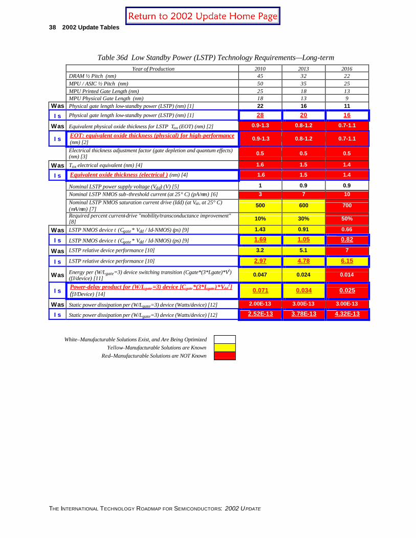
38 2002 Update Tables
THE INTERNATIONAL TECHNOLOGY ROADMAP FOR SEMICONDUCTORS: 2002 UPDATE
Table 36d Low Standby Power (LSTP) Technology Requirements—Long-term Year of Production 2010 2013 2016 DRAM ½ Pitch (nm) 45 32 22 MPU / ASIC ½ Pitch (nm) 50 35 25 MPU Printed Gate Length (nm) 25 18 13 MPU Physical Gate Length (nm) 18 13 9
Was Physical gate length low-standby power (LSTP) (nm) [1] 22 16 11
Is Physical gate length low-standby power (LSTP) (nm) [1] 28 20 16
Was Equivalent physical oxide thickness for LSTP Tox (EOT) (nm) [2] 0.9-1.3 0.8-1.2 0.7-1.1
Is EOT: equivalent oxide thickness (physical) for high-performance (nm) [2]
0.9-1.3 0.8-1.2 0.7-1.1
Electrical thickness adjustment factor (gate depletion and quantum effects) (nm) [3] 0.5 0.5 0.5
Was Tox electrical equivalent (nm) [4] 1.6 1.5 1.4
Is Equivalent oxide thickness (electrical ) (nm) [4] 1.6 1.5 1.4
Nominal LSTP power supply voltage (Vdd) (V) [5] 1 0.9 0.9
Nominal LSTP NMOS sub-threshold current (at 25° C) (pA/µm) [6] 3 7 10
Nominal LSTP NMOS saturation current drive (Idd) (at Vdd, at 25° C) (µA/µm) [7]
500 600 700
Required percent current-drive "mobility/transconductance improvement" [8] 10% 30% 50%
Was LSTP NMOS device τ (Cgate * Vdd / Id-NMOS) (ps) [9] 1.43 0.91 0.66
Is LSTP NMOS device τ (Cgate * Vdd / Id-NMOS) (ps) [9] 1.69 1.05 0.82
Was LSTP relative device performance [10] 3.2 5.1 7
Is LSTP relative device performance [10] 2.97 4.78 6.15
Was Energy per (W/Lgate=3) device switching transition (Cgate*(3*Lgate)*V2) (fJ/device) [11]
0.047 0.024 0.014
Is Power-delay product for (W/L gate=3) device [C gate*(3*L gate)*V dd2]
(fJ/Device) [14] 0.071 0.034 0.025
Was Static power dissipation per (W/Lgate=3) device (Watts/device) [12] 2.00E-13 3.00E-13 3.00E-13
Is Static power dissipation per (W/Lgate=3) device (Watts/device) [12] 2.52E-13 3.78E-13 4.32E-13
White–Manufacturable Solutions Exist, and Are Being Optimized Yellow–Manufacturable Solutions are Known
Red–Manufacturable Solutions are NOT Known

2002 Update Tables 39
THE INTERNATIONAL TECHNOLOGY ROADMAP FOR SEMICONDUCTORS: 2002 UPDATE
Notes for Table 36a through d:
[1] Values set by ORTC.
[1] Values set by ORTC. Assumed to lag high-performance scaling by 2 years. Gate dimensional control is set by the Lithography and FEP (Etch) ITWGs and is assumed to have a three sigma value of ±10%. Gate dimension variation is assumed to be the primary factor responsible for driving device parameter variation. Gate length for the LOP and LSTP devices are assumed to be identical.
Was
[2] EOT value set by FEP ITWG in the Front End Processes chapter, Thermal and Thin Film, Doping, and Etching Technology Requirements tables Yellow/red feasibility coloring set by FEP ITWG projections on gate leakage, thickness control and reliability capability (high κ gate dielectrics will be required around 2005 in order to suppress gate leakage for LSTP). Due to different system applications, the EOT values for the LOP and LSTP devices have been optimized and set independently of each other. Calculations in rest of PIDS table (and the underlying PIDS workbook) based on approximate midpoint EOT values
Is
[2] ] EOT value set by FEP ITWG in the Front End Processes chapter, Thermal and Thin Film, Doping, and Etching Technology Requirements tables Yellow/red feasibility coloring set by FEP ITWG projections on gate leakage, thickness control and reliability capability (high κ gate dielectrics will be required around 2005 in order to suppress gate leakage for LSTP). Due to different system applications, the EOT values for the LOP and LSTP devices have been optimized and set independently of each other. Calculations in rest of PIDS table (and the underlying PIDS workbook) based on approximate midpoint EOT values. For a gate dielectric of thickness T d and relative dielectric constant k, EOT is defined by: EOT = Td / (k/3.9), where 3.9 is the relative dielectric constant of thermal silicon dioxide. The ideal gate capacitance per unit area of the gate dielectric of thickness Td is the same as that of a gate dielectric made up of thermal silicon dioxide with a thickness of EOT.
[3] Accounts for gate electrode depletion and inversion-layer quantum effects. Yellow feasibility coloring reflects FEP assessment of polysilicon doping capability; red feasibility coloring reflects the introduction of metal-gate electrodes by 2007 (which reduces the gate depletion value).
[4] Sum of midpoint EOT and Electrical Thickness Adjustment Factor. Used in CV/I performance metric and CV2 dynamic power metric calculations. Red/yellow feasibility coloring determined by worst-case EOT and Electrical Thickness Adjustment Factor red/yellow feasibility coloring.
Was
[5] Nominal power supply voltage which has been set to smallest value to still maintain sufficient voltage over-drive to allow sufficient circuit switching noise margin (approximately 2.3 times the threshold voltage). Actual power supply voltage values may vary ± 10%, depending on the particular circuit design application or technology optimization. Due to different system applications, the power-supply voltages for the LOP and LSTP devices have been optimized and set independently of each other. Note, meeting overall system power dissipation requirements will require the use of circuit/system techniques to "turn -off" or "power-down" various circuit blocks.
Is
[5] Nominal power supply voltage which has been set to smallest value to still maintain sufficient voltage over-drive to allow sufficient circuit switching noise margin (approximately 2.3 times the threshold voltage). Actual power supply voltage target values may vary ± 10%, depending on the particular circuit design application or technology optimization. Due to different system applications, the power-supply voltages for the LOP and LSTP devices have been optimized and set independently of each other. Note, meeting overall system power dissipation requirements will require the use of circuit/system techniques to "turn -off" or "power-down" various circuit blocks.
Was
[6] Nominal sub-threshold leakage current is defined as the NMOSFET source current at room temperature with the drain bias set equal to the nominal power-supply voltage and with the gate, source, and substrate biases set to zero volts; all MOSFET device dimensions are assumed to be at their nominal/target values. Total NMOS off-state current is the NMOSFET drain current at room temperature, and is the sum of the NMOS sub-threshold, gate, and junction leakage current components. The sub-threshold leakage current is assumed to be larger than either the gate or junction current components at either room or high-temperature conditions. The increase in sub-threshold current (and the corresponding threshold -voltage value reduction) has been set at a pace that lags the rate of increase of the high-performance device, but that still increases sufficiently to enable continued device performance scaling; power dissipation due to off-state leakage is assumed to not exceed 10% of the total chip power, which is assumed to be 100mW in 2001 and 200mW in 2010 for LOP. For LOP, the yellow feasibility coloring reflects the difficulty of meeting the gate leakage requirements with thin oxy-nitride films and the potential need for non-classical CMOS or ultra-shallow junction technology by 2007 to control short-channel effects and to limit lateral high-field effects. For LSTP, the yellow feasibility coloring in 2003 and 2004 reflects the difficulty of meeting the gate leakage requirements with thin oxy-nitride gate dielectric films, while the red feasibility color from 2005 on reflects the difficulty of implementing a high κ gate dielectric to meet the gate leakage requirements. The above sub-threshold, gate, and junction current scaling scenario also applies to PMOS devices.
Is
[6] ] Nominal sub-threshold leakage current is defined as the NMOSFET source current at room temperature with the drain bias set equal to the nominal power-supply voltage and with the gate, source, and substrate biases set to zero volts; all MOSFET device dimensions are assumed to be at their nominal/target values. Total NMOS off-state current is the NMOSFET drain current at room temperature, and is the sum of the NMOS sub-threshold, gate, and junction leakage current components. The sub-threshold leakage current is assumed to be larger than either the gate or junction current components at eith er room or high-temperature conditions. The increase in sub-threshold current (and the corresponding threshold -voltage value reduction) has been set at a pace that lags the rate of increase of the high-performance device, but that still increases sufficiently to enable continued device performance scaling; power dissipation due to off-state leakage is assumed to not exceed 10% of the total chip power, which is assumed to be 100mW in 2001 and 200mW in 2010 for LOP. For LOP, the yellow feasibility coloring reflects the difficulty of meeting the gate leakage requirements with thin oxy-nitride films and the potential need for non-classical CMOS or ultra-shallow junction technology by 2007 to control short-channel effects and to limit lateral high-field effects. For LSTP, the yellow feasibility coloring in 2003 and 2004 reflects the difficulty of meeting the gate leakage requirements with thin oxy-nitride gate dielectric films, while the red feasibility color from 2005 on reflects the difficulty of implementing a high κ gate dielectric to meet the gate leakage requirements. The above sub-threshold, gate, and junction current scaling scenario also applies to PMOS devices.

40 2002 Update Tables
THE INTERNATIONAL TECHNOLOGY ROADMAP FOR SEMICONDUCTORS: 2002 UPDATE
Notes for Table 36a through d (continued):
[7] Nominal saturation current drive is defined as the MOSFET drain current at room temperature with the gate bias and the drain bias set equal to the nominal power-supply voltage; all MOSFET device dimensions are assumed to be at their nominal/target values. Nominal PMOS saturation current-drive value is assumed to be 40–50% of the nominal NMOS saturation current-drive value. Yellow/red feasibility coloring indicates the projected need for fundamental device current-drive (transconductance/mobility) improvement by 2010 in order to continue approximate 14% per year device performance scaling. NMOS/PMOS current-drive targets are approximate with only 1.5 significant digits of accuracy. The sub-threshold slope, parasitic source/drain resistance, and parasitic gate capacitance scaling have been assumed to be similar to that for the high-performance device. (See the enclosed Excel workbook for the detailed calculations).
[8] Fundamental device mobility/transconductance improvement needed by 2010 in order to continue historical approximate 14% per year device performance scaling. Yellow/red feasibility coloring indicates the difficulty of implementing the fundamental device current-drive (transconductance/mobility) improvement required in 2010 and beyond to continue historical approximate 14% per year device performance scaling. The LOP and LSTP required improvement is projected as lagging that required for the high-performance device.
Was [9] τ = CV/I intrinsic delay metric for NMOS device; PMOS CV/I metric assumed to scale proportionally. The CV/I metric provides an indication of the intrinsic switching delay of the device, while 1/τ, the reciprocal of CV/I, is a good metric for the intrinsic switching speed of the device. Red/yellow feasibility coloring determined by saturation current-drive feasibility coloring. The C term includes the effect of parasitic gate capacitance, which has been assumed to be equivalent to that for the high-performance device.
Is
[9] ] τ = CV/I intrinsic delay metric for NMOS device; PMOS CV/I metric assumed to scale proportionally. The CV/I metric provides an indication of the intrinsic switching delay of the device, while 1/τ, the reciprocal of CV/I, is a good metric for the intrinsic switching speed of the device. Red/yellow feasibility coloring determined by saturation current-drive feasibility coloring. The C (gate capacitance) includes the effect of parasitic gate capacitance, which has been assumed to be equivalent to that for the high-performance device. For LSTP, τ has been adjusted to reflect the change in scaling of the physical gate length compared to the 2001 ITRS.
Was [10] Improvement in 1/τ NMOS performance metric normalized to the year 2001. Maintains approximate 14% per year device performance improvement scaling trend for both LOP and LSTP. Red/yellow feasibility coloring determined by saturation current-drive feasibility coloring.
Is
10] [10] Improvement in 1/τ NMOS performance metric normalized to the year 2001. Maintains approximate 14% per year device performance improvement scaling trend for both LOP and LSTP. Red/yellow feasibility coloring determined by saturation current-drive feasibility coloring. For LSTP, 1/τ has been adjusted to reflect the change in scaling of the physical gate length compared to the 2001 ITRS.
Was [11] CV2switching energy metric for an NMOS device with dimensions W/Lgate=3. The switching energy metric indicates the amount of dynamic power required to switch the device. Red/yellow feasibility coloring determined by sa turation current-drive feasibility coloring.
Is
[11] ] CV2switching energy metric for an NMOS device with dimensions W/Lgate=3. The power-delay product indicates the amount of dynamic energy required to switch the device through a full (up and down) transition. Red/yellow feasibility coloring determined by saturation current-drive feasibility coloring. For LSTP, the power-delay product has been adjusted to reflect the change in scaling of the physical gate length compared to the 2001 ITRS.
Was [12] Static power dissipation for an NMOS device with dimensions W/Lgate=3. Assume that the device static power is primarily determined by the sub-threshold current (since the other junction and leakage current components are assumed to be lower). Yellow/red feasibility coloring is determined by the sub-threshold leakage current feasibility coloring.
Is
[12] Static power dissipation for an NMOS device with dimensions W/Lgate=3. Assume that the device static power is primarily determined by the sub-threshold current (since the other junction and leakage current components are assumed to be lower). Yellow/red feasibility coloring is determined by the sub-threshold leakage current feasibility coloring. For LSTP, the static power dissipation per device has been adjusted to reflect the change in scaling of the physical gate length compared to the 2001 ITRS.

2002 Update Tables 41
THE INTERNATIONAL TECHNOLOGY ROADMAP FOR SEMICONDUCTORS: 2002 UPDATE
Table 37a DRAM Technology Requirements—Near-term
Year of Production 2001 2002 2003 2004 2005 2006 2007
DRAM ½ Pitch (nm)[1] 130 115 100 90 80 70 65
MPU / ASIC ½ Pitch (nm) 150 130 107 90 80 70 65
MPU Printed Gate Length (nm) 90 75 65 53 45 40 35
MPU Physical Gate Length (nm) 65 53 45 37 32 28 25
DRAM cell size (µm2) [2] 0.135 0.106 0.06 0.049 0.038 0.029 0.025
DRAM storage cell dielectric: equivalent physical oxide thickness, EOT (nm) [3] 2.04 1.8 1.2 1 0.45 0.32 0.22
Was DRAM retention time (ms) [4] 64 64 64 64 64 64 64
Is Minimum DRAM retention time (ms) [4] 64 64 64 64 64 64 64
DRAM soft error rate (fits) [5] 1000 1000 1000 1000 1000 1000 1000
Table 37b DRAM Technology Requirements—Long-term
Year of Production 2010 2013 2016
DRAM ½ Pitch (nm) [1] 45 32 22
MPU / ASIC ½ Pitch (nm) 50 35 25
MPU Printed Gate Length (nm) 25 18 13
MPU Physical Gate Length (nm) 18 13 9
DRAM cell size (µm2) [2] 0.0122 0.0041 0.0019
DRAM storage cell dielectric: equivalent physical oxide thickness, EOT (nm) [3] 0.084 0.028 0.01
Was DRAM retention time (ms) [4] 64 64 64
Is Minimum DRAM retention time (ms) [4] 64 64 64
DRAM soft error rate (fits) [5] 1000 1000 1000
White–Manufacturable Solutions Exist, and Are Being Optimized Yellow–Manufacturable Solutions are Known
Red–Manufacturable Solutions are NOT Known
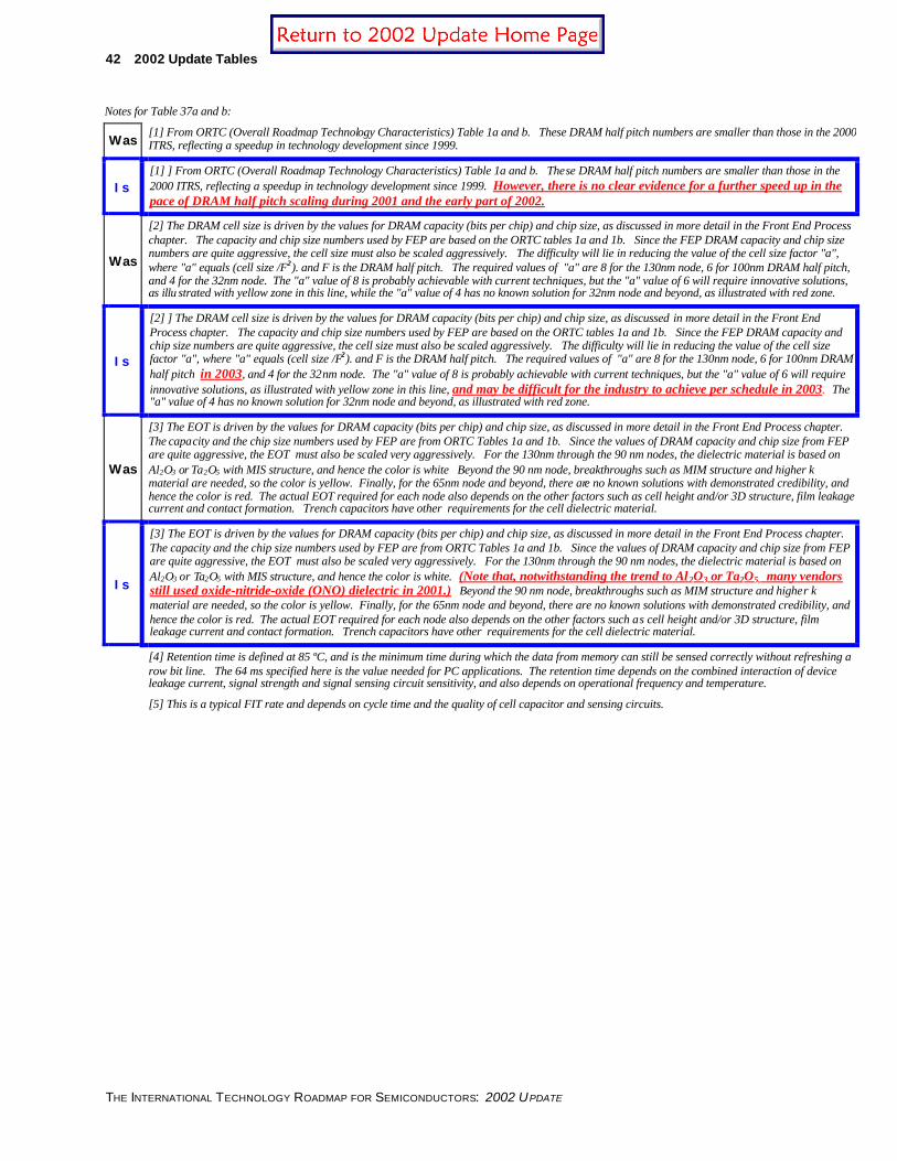
42 2002 Update Tables
THE INTERNATIONAL TECHNOLOGY ROADMAP FOR SEMICONDUCTORS: 2002 UPDATE
Notes for Table 37a and b:
Was [1] From ORTC (Overall Roadmap Technology Characteristics) Table 1a and b. These DRAM half pitch numbers are smaller than those in the 2000 ITRS, reflecting a speedup in technology development since 1999.
Is [1] ] From ORTC (Overall Roadmap Technology Characteristics) Table 1a and b. These DRAM half pitch numbers are smaller than those in the 2000 ITRS, reflecting a speedup in technology development since 1999. However, there is no clear evidence for a further speed up in the pace of DRAM half pitch scaling during 2001 and the early part of 2002.
Was
[2] The DRAM cell size is driven by the values for DRAM capacity (bits per chip) and chip size, as discussed in more detail in the Front End Process chapter. The capacity and chip size numbers used by FEP are based on the ORTC tables 1a and 1b. Since the FEP DRAM capacity and chip size numbers are quite aggressive, the cell size must also be scaled aggressively. The difficulty will lie in reducing the value of the cell size factor "a", where "a" equals (cell size /F2). and F is the DRAM half pitch. The required values of "a" are 8 for the 130nm node, 6 for 100nm DRAM half pitch, and 4 for the 32nm node. The "a" value of 8 is probably achievable with current techniques, but the "a" value of 6 will require innovative solutions, as illu strated with yellow zone in this line, while the "a" value of 4 has no known solution for 32nm node and beyond, as illustrated with red zone.
Is
[2] ] The DRAM cell size is driven by the values for DRAM capacity (bits per chip) and chip size, as discussed in more detail in the Front End Process chapter. The capacity and chip size numbers used by FEP are based on the ORTC tables 1a and 1b. Since the FEP DRAM capacity and chip size numbers are quite aggressive, the cell size must also be scaled aggressively. The difficulty will lie in reducing the value of the cell size factor "a", where "a" equals (cell size /F2). and F is the DRAM half pitch. The required values of "a" are 8 for the 130nm node, 6 for 100nm DRAM half pitch in 2003, and 4 for the 32nm node. The "a" value of 8 is probably achievable with current techniques, but the "a" value of 6 will require innovative solutions, as illustrated with yellow zone in this line, and may be difficult for the industry to achieve per schedule in 2003. The "a" value of 4 has no known solution for 32nm node and beyond, as illustrated with red zone.
Was
[3] The EOT is driven by the values for DRAM capacity (bits per chip) and chip size, as discussed in more detail in the Front End Process chapter. The capacity and the chip size numbers used by FEP are from ORTC Tables 1a and 1b. Since the values of DRAM capacity and chip size from FEP are quite aggressive, the EOT must also be scaled very aggressively. For the 130nm through the 90 nm nodes, the dielectric material is based on Al2O3 or Ta2O5 with MIS structure, and hence the color is white Beyond the 90 nm node, breakthroughs such as MIM structure and higher κ material are needed, so the color is yellow. Finally, for the 65nm node and beyond, there are no known solutions with demonstrated credibility, and hence the color is red. The actual EOT required for each node also depends on the other factors such as cell height and/or 3D structure, film leakage current and contact formation. Trench capacitors have other requirements for the cell dielectric material.
Is
[3] The EOT is driven by the values for DRAM capacity (bits per chip) and chip size, as discussed in more detail in the Front End Process chapter. The capacity and the chip size numbers used by FEP are from ORTC Tables 1a and 1b. Since the values of DRAM capacity and chip size from FEP are quite aggressive, the EOT must also be scaled very aggressively. For the 130nm through the 90 nm nodes, the dielectric material is based on Al2O3 or Ta2O5 with MIS structure, and hence the color is white. (Note that, notwithstanding the trend to Al 2O 3 or Ta 2O 5, many vendors still used oxide-nitride-oxide (ONO) dielectric in 2001.) Beyond the 90 nm node, breakthroughs such as MIM structure and higher κ material are needed, so the color is yellow. Finally, for the 65nm node and beyond, there are no known solutions with demonstrated credibility, and hence the color is red. The actual EOT required for each node also depends on the other factors such as cell height and/or 3D structure, film leakage current and contact formation. Trench capacitors have other requirements for the cell dielectric material.
[4] Retention time is defined at 85 ºC, and is the minimum time during which the data from memory can still be sensed correctly without refreshing a row bit line. The 64 ms specified here is the value needed for PC applications. The retention time depends on the combined interaction of device leakage current, signal strength and signal sensing circuit sensitivity, and also depends on operational frequency and temperature.
[5] This is a typical FIT rate and depends on cycle time and the quality of cell capacitor and sensing circuits.

2002 Update Tables 43
THE INTERNATIONAL TECHNOLOGY ROADMAP FOR SEMICONDUCTORS: 2002 UPDATE
Table 38a Non-Volatile Memory Technology Requirements—Near-term Year of Production 2001 2002 2003 2004 2005 2006 2007 DRAM ½ Pitch (nm) 130 115 100 90 80 70 65 MPU / ASIC ½ Pitch (nm) 150 130 107 90 80 70 65 MPU Printed Gate Length (nm) 90 75 65 53 45 40 35 MPU Physical Gate Length (nm) 65 53 45 37 32 28 25
Was Flash technology node - F (nm) [1] 150 130 115 100 90 80 70
Is Flash technology node - F (nm) [1] 150 130 107 90 80 70 65
Flash NOR cell size –area factor a in multiples of F2[2] 10–12 10–12 10–12 11–14 11–14 11–14 11–14 Was Flash NAND cell size ––area factor a in multiples of F2 SLC/MLC [3] 5.5 5.5 4.5 4.5 4.5 4.5/2.3 4.5/2.3
Is Flash NAND cell size ––area factor a in multiples of F2 SLC/MLC [3] 5.5 5.5 5.5 5.5 5.5 5.5 4.5
Was Flash NOR typical cell size (µm2) [4] 0.248 0.186 0.145 0.125 0.101 0.08 0.061
Is Flash NOR typical cell size (µm2) [4] 0.248 0.186 0.135 0.101 0.08 0.061 0.061
Was Flash NOR Lg -stack (physical- µm) [5] 0.29–0.310.25–0.270.22–0.24 0.21–0.23 0.2–0.22 0.2–0.22 0.19–0.21
Is Flash NOR Lg-stack (physical- µm) [5] 0.29–0.310.25–0.270.22–0.24 0.2–0.22 0.2–0.22 0.19–0.21 0.19–0.21
Was Flash NOR highest W/E voltage (V) [6] 8–10 8–10 8–10 8–10 7–9 7–9 7–9
Is Flash NOR highest W/E voltage (V) [6] 8–10 8–10 8–10 7–9 7–9 7–9 7–9
Was Flash NAND highest W/E voltage (V) [7] 19–21 18–20 18–20 18–20 18–20 17–19 17–19
Is Flash NAND highest W/E voltage (V) [7] 19–21 18–20 18–20 17-19 17-19 17-19 15-17
Was Flash NOR Iread (µA) [8] 36–44 35–43 34–42 33–41 31–39 28–36 29–37
Is Flash NOR Iread (µA) [8] 36–44 35–43 34–42 31–39 29-37 28-36 27-35 Was Flash Coupling Ratio [9] 0.65–0.750.65–0.750.65–0.75 0.65–0.75 0.65–0.75 0.65–0.75 0.6–0.7
Is Flash Coupling Ratio [9] 0.65–0.750.65–0.750.65–0.75 0.65–0.750.65–0.75 0.6–0.7 0.6–0.7
Was Flash NOR tunnel oxide thickness (nm) [10] 9.5–10.5 9.5–10 9–10 9–10 8.5–9.5 8.5–9.5 8.5–9.5
Is Flash NOR tunnel oxide thickness (nm) [10] 9.5-10.5 9-10 9-10 8.5-9.5 8.5-9.5 8.5-9.5 8-9
Was Flash NAND tunnel oxide thickness (nm) [11] 8.5–9.5 8.5–9 8–9 8–9 8–9 7.5–8 7.5–8
Is Flash NAND tunnel oxide thickness (nm) [11] 8.5-9.5 7-8 7-8 7-8 7-8 7-8 6-7 Was Flash NOR interpoly dielectric thickness (nm) [12] 13–15 12–14 11–13 11–13 10–12 9–11 9–11
Is Flash NOR interpoly dielectric thickness (nm) [12] 13-15 12-14 11-13 10-12 9-11 9-11 8.5-10.5
Was Flash NAND interpoly dielectric thickness (nm) [13] 14–16 13–15 12–14 12–14 12–14 11–13 10–12
Is Flash NAND interpoly dielectric thickness (nm) [13] 14-16 13-15 13-15 13-15 13-15 13-15 10-13
Flash endurance (erase/write cycles) [14] 1.00E+05 1.00E+05 1.00E+05 1.00E+05 1.00E+05 1.00E+05 1.00E+05 Flash nonvolatile data retention (years) [15] 10 10–20 10–20 10–20 10–20 10–20 10–20 Flash maximum number of bits per cell (MLC) [16] 2 2 4 4 4 4 4 FeRAM technology node - F (nm) [17] 500 350 250 220 180 150 130 FeRAM cell size —area factor a in multiples of F2 [18] 60 40 24 16 10 10 10 FeRAM cell size (µm2) [19] 15 4.9 1.5 0.518 0.324 0.225 0.169 FeRAM cell structure [20] 2T2C 1T1C 1T1C 1T1C 1T1C 1T1C 1T1C FeRAM capacitor structure [21] planar planar stack stack stack stack 3D Ferro capacitor voltage (V) [22] 3 3 2.5 1.8 1.5 1.3 1.2 FeRAM endurance (read/write cycles) [23] 1.00E+12 1.00E+13 1.00E+14 1.00E+15 >1E16 >1E16 >1E16 FeRAM nonvolatile data retention (years) [24] 10 10 10 10 10 10 10
White–Manufacturable Solutions Exist, and Are Being Optimized
Yellow–Manufacturable Solutions are Known
Red–Manufacturable Solutions are NOT Known

44 2002 Update Tables
THE INTERNATIONAL TECHNOLOGY ROADMAP FOR SEMICONDUCTORS: 2002 UPDATE
Table 38b Non-Volatile Memory Technology Requirements—Long-term Year of Production 2010 2013 2016
DRAM ½ Pitch (nm) 45 32 22
MPU / ASIC ½ Pitch (nm) 50 35 25
MPU Printed Gate Length (nm) 25 18 13
MPU Physical Gate Length (nm) 18 13 9
Flash technology node - F (nm) [1] 50 35 25
Flash NOR cell size -–area factor a in multiples of F2[2] 12–15 13–16 14–17
Flash NAND cell size -–area factor a in multiples of F2 SLC/MLC [3] 4.5/2.3 4.5/2.3 4.5/2.3
Flash NOR typical cell size (µm2) [4] 0.034 0.018 0.01
Flash NOR Lg -stack (physical- µm) [5] 0.17–0.190.14–0.160.12–0.14
Flash NOR highest W/E voltage (V) [6] 7–9 7–9 7–9
Was Flash NAND highest W/E voltage (V) [7] 17–19 16–18 16–18
Is Flash NAND highest W/E voltage (V) [7] 15-17 15-17 15-17
Flash NOR I_read (µA) [8] 27–33 25–31 22–28
Flash Coupling Ratio [9] 0.6–0.7 0.6–0.7 0.6–0.7
Flash NOR tunnel oxide thickness (nm) [10] 8–9 8 8
Flash NAND tunnel oxide thickness (nm) [11] 6–7 6–7 6–7
Flash NOR interpoly dielectric thickness (nm) [12] 8–10 6–8 4–6
Was Flash NAND interpoly dielectric thickness (nm) [13] 10–12 9–11 9–11
Is Flash NAND interpoly dielectric thickness (nm) [13] 10-13 9-10 9-10
Flash endurance (erase/write cycles) [14] 1.00E+06 1.00E+06 1.00E+07
Flash nonvolatile data retention (years) [15] 10–20 20 20
Flash maximum number of bits per cell (MLC) [16] 8 8 8
FeRAM technology node - F (nm) [17] 100 70 50
FeRAM cell size -–area factor a in multiples of F 2 [18] 8 8 8
FeRAM cell size (µm2) [19] 0.08 0.039 0.02
FeRAM cell structure [20] 1T1C 1T1C 1T1C
FeRAM capacitor structure [21] 3D 3D 3D
Ferro capacitor voltage (V) [22] 1 0.7 0.7
FeRAM endurance (read/write cycles) [23] >1E16 >1E16 >1E16
FeRAM nonvolatile data retention (years) [24] 10 10 10
White–Manufacturable Solutions Exist, and Are Being Optimized Yellow–Manufacturable Solutions are Known
Red–Manufacturable Solutions are NOT Known

2002 Update Tables 45
THE INTERNATIONAL TECHNOLOGY ROADMAP FOR SEMICONDUCTORS: 2002 UPDATE
FRONT END PROCESSES Table 48 Front End Processes Difficult Challenges
MPU/ASIC Physical Gate Length ≥ 25 nm,
Through 2007 Summary of Issues
New gate stack processes and materials
Extension of oxy-nitride gate dielectric materials to < 1.0nm E.O.T for high performance MOSFETs, consistent with device reliability requirements
Introduction and process integration of high κ gate stack materials and processes for low operating and low standby power MOSFETs
Control of boron penetration from doped polysilicon gate electrode
Minimized depletion of dual-doped polysilicon electrodes
Possible introduction of dual-metal gate electrodes with appropriate work function (toward end of period)
Metrology issues associated with gate dielectric film thickness and stack electrical and materials characterization
WasCritical dimension and effective
channel length (Leff) control
Control of gate etch process that yield a physical gate length that is smaller than the feature size printed in the resist, while maintaining <10% overall 3-sigma control of the combined lithography and etch processes
Control of profile shape, edge roughness, line and space width for isolated as well as closely -spaced fine line patterns
Control of self-aligned doping processes and thermal activation budgets to achieve ~15% 3σ Leff control
Maintenance of CD and profile Control throughout the transition to new gate stack materials and processes
CD and etch metrology
Is Critical dimension and effective channel length (Leff) control
Control of gate etch process that yield a physical gate length that is smaller than the feat ure size printed in the resist, while maintaining <10% overall 3-sigma control of the combined lithography and etch processes
Control of profile shape, edge roughness, line and space width for isolated as well as closely -spaced fine line patterns
Control of self-aligned doping processes and thermal activation budgets to achieve ~15% 3σ Leff control
Maintenance of CD and profile Control throughout the transition to new gate stack materials and processes
CD and etch metrology
CMOS integration of new memory materials and processes
Development and introduction of very high κ DRAM capacitor dielectric layers
Migration of DRAM capacitor structures from silicon-insulator-metal to metal-insulator-metal
Integration and scaling of FeRAM ferroelectric materials
Scaling of Flash inter-poly and tunnel dielectric layers may require high κ
Limited temperature stability of high κ and ferroelectric materials challenges CMOS integration
Surfaces and interfaces: structure, composition and contamination control
Contamination, composition, and structure control of channel/gate dielectric interface as well as gate dielectric/gate electrode interface
Interface control for DRAM capacitor structures
Maintenance of surface and interface integrity through full-flow CMOS processing
Statistically significant characterization of surfaces having extremely low defect concentrations for starting materials and pre-gate clean surfaces
Scaled MOSFET dopant introduction and control
Doping and activation processes to achieve shallow source/drain regions having parasitic resistance that is less than ~16–20% of ideal channel resistance (=Vdd/Ion)
Control of parasitic capacitance to achieve less than ~19–27% of gate capacitance, consistent with acceptable Ion and minimum short channel effect
Achievement of activated dopant concentration greater than solid solubility in dual-doped polysilicon gate electrodes
Formation of continuous self-aligned silicide contacts over shallow source and drain regions
Metrology issues associated with 2D dopant profiling

46 2002 Update Tables
THE INTERNATIONAL TECHNOLOGY ROADMAP FOR SEMICONDUCTORS: 2002 UPDATE
Table 48 Front End Processes Difficult Challenges(continued)
MPU/ASIC physical Gate Length <25 nm, Beyond 2007 Issues Continued scaling of planar CMOS devices Higher κ gate dielectric materials including temperature constraints
Metal gate electrodes with appropriate work function
Sheet resistance of clad junctions
Enhanced channel mobility, e.g., strained layers
CD and Leff control
Chemical, electrical and structural characterization
Introduction and CMOS integration of non-standard, double gate MOSFET devices
Devices may be needed as early as 2007
Selection and characterization of optimum device types
CMOS integration with other devices, including planar MOSFETs
Introduction, characterization and production hardening of new FEP unit processes
Device and FEP process metrology
Increased funding of long term research
Starting silicon material alternatives beyond 300 mm Need for future productivity enhancement dictates the requirement for a next generation, large silicon substrate material
Historical trends suggest that the new starting material have nominally twice the area of present generation substrates, e.g., 450 mm
Economies of the incumbent Czochralski crystal pulling, wafer slicing and polishing processes are questionable beyond 300 mm; research is required for a cost-effective substrate alternative to bulk silicon
New memory storage cells, storage devices, and memory architectures
Scaling of DRAM storage capacitor beyond 6F2 and ultimately beyond 4F2
Further scaling of Flash memory interpoly and tunnel oxide thickness
FeRAM storage cell scaling
Introduction of new memory types and storage concepts
Surface and interface structural, contamination, and compositional control
Achievement and maintenance of structural, chemical and contamination control of surfaces and interfaces, that may be horizontally or vertically oriented relative to the chip surface
Metrology and characterization of surfaces that may be horizontally or vertically oriented relative to the chip surface
Achievement of statistically significant characterization of surfaces and interfaces that may be horizontally or vertically oriented relative to the chip surface

2002 Update Tables 47
THE INTERNATIONAL TECHNOLOGY ROADMAP FOR SEMICONDUCTORS: 2002 UPDATE
Corrected Starting Materials Requirements Cell Key for Table 49a and b
Strained Si:Ge on SOI
Recommend addition of comment below to 2002 ITRS update as follows:
Strained silicon films to enhance carrier mobility typically are formed on relaxed SixGe1-x for NMOSFETS. However, for PMOSFET applications, strained Si may be fabricated on strained SixGe1-x or strained SixGe1-x may be utilized in place of the strained Si on strained SixGe1-x for the channel region. Both SOI-like structures and bulk silicon may be utilized, although the former appears to be preferred for enhanced device performance.
Starting Materia ls sub TWG will address strained Si:Ge in further detail in the 2003 ITRS revision.
Starting Materials Requirements Cell Key
White-Maintenance Item
Yellow-Process Margin Iimprovement
Technology requirements value and supplier manufacturing capability
Criticality of requirement to IC wafer user
Metrology readiness capability
Red-"Showstopper"
Color-Code Key
White-Manufacturable Solutions Exist and Are Being Optimized
Yellow-Manufacturable Solutions are Known
Red-Manufacturable Solutions are NOT Known
Technology requirements value and supplier manufacturing capability cells and metrology
readiness capability cells
Criticality of requirement to IC wafer user cells

48 2002 Update Tables
THE INTERNATIONAL TECHNOLOGY ROADMAP FOR SEMICONDUCTORS: 2002 UPDATE
Table 49a Starting Materials Technology Requirements—Near-term Year of Production 2001 2002 2003 2004 2005 2006 2007 DRIVER
DRAM ½ Pitch (nm) 130 115 100 90 80 70 65 D ½ MPU / ASIC ½ Pitch (nm) 150 130 107 90 80 70 65 M MPU Printed Gate Length (nm) 90 75 65 53 45 40 35 M MPU Physical Gate Length (nm) 65 53 45 37 32 28 25 M
DRAM Total Chip Area (mm2) 127 100 118 93 147 116 183 D ½
DRAM Active Transistor Area (mm2) 55.3 36.9 59.0 42.3 73.1 53.2 89.9 D ½
MPU High-Performance Total Chip Area (mm2)
310 310 310 310 310 310 310 M
MPU High-Performance Active Transistor Area (mm2)
28.7 28.2 27.7 27.2 26.8 26.8 26.8 M
General Characteristics * (99% Chip Yield) [A,B,C] Wafer diameter (mm) ** 300*** 300*** 300*** 300 300 300 300 D ½, M
3 3 2 2 2 2 2 D ½, M Edge exclusion (mm) ****
≥ 90 ≥ 90 ≥ 90 ≥45 ≥40 ≥35 ≥33 D ½, M Front surface particle size (nm), latex sphere equivalent [D] € € € €
≤ 0.18 ≤ 0.27 ≤ 0.17 ≤ 0.24 ≤ 0.14 ≤ 0.19 ≤ 0.11 D ½ Particles (cm–2) [E]
≤ 123 ≤ 185 ≤ 117 ≤ 164 ≤ 95 ≤ 130 ≤ 77 D ½ Particles (#/wf)
≤ 1 E10 ≤ 1 E10 ≤ 1 E10 ≤ 1 E10 ≤ 1 E10 ≤ 1 E10 ≤ 1 E10 D ½, M
Critical surface metals (at/cm2) [F] ≤ 130 ≤ 115 ≤ 100 ≤ 90 ≤ 80 ≤ 70 ≤ 65 D ½, M
Site flatness (nm) [G]
Polished Wafer * (99% Chip Yield) The LLS requirement is specified for particles only; discrimination between particles and COPs is required (see General Characteristics) [D,E]
≤ 1 E10 ≤ 1 E10 ≤ 1 E10 ≤ 1 E10 ≤ 1 E10 ≤ 1 E10 ≤ 1 E10 D ½, M Total bulk Fe (at/cm3) [H]
€ ≤ 2.8 ≤ 2.3 ≤ 1.9 ≤ 1.6 ≤ 1.4 ≤?1.1 ≤ 1.0 D ½ Oxidation stacking faults (OSF)
(DRAM) (cm–2) [I] ≤ 1.0 ≤ 0.8 ≤ 0.6 ≤ 0.5 ≤ 0.4 ≤ 0.3 ≤ 0.3 M Oxidation stacking faults (OSF)
(MPU) (cm–2) [I] Epitaxial Wafer * (99% Chip Yield) Total Allowable Front Surface Defect Density is The Sum of Epitaxial Large Structural Defects, Small Structural Defects and Particles (see General Characteristics) [J,K]
≤ 0.008 ≤ 0.010 ≤ 0.009 ≤ 0.011 ≤ 0.007 ≤ 0.009 ≤ 0.005 D ½ Large structural epi defects (DRAM) (cm–2) [L]
≤ 0.003 ≤ 0.003 ≤ 0.003 ≤ 0.003 ≤ 0.003 ≤ 0.003 ≤ 0.003 M Large structural epi defects (MPU) (cm–2) [L]
≤ 0.016 ≤ 0.020 ≤ 0.017 ≤ 0.022 ≤ 0.014 ≤ 0.017 ≤ 0.011 D ½ Small structural epi defects (DRAM) (cm–2) [M]
≤ 0.006 ≤ 0.006 ≤ 0.006 ≤ 0.006 ≤ 0.006 ≤ 0.006 ≤ 0.006 M Small structural epi defects (MPU) (cm–2) [M]
Table Cell Key Legend
Color-Code Key
Criticality of requirement to IC wafer user
Metrology readiness capability
White-Maintenance Item
Yellow-Process Margin Iimprovement
Criticality of requirement to IC wafer user cells
Technology requirements value and supplier manufacturing capability
Red-"Showstopper"
White-Manufacturable Solutions Exist and Are Being Optimized
Yellow-Manufacturable Solutions are KnownRed-Manufacturable Solutions are NOT Known
Technology requirements value and supplier manufacturing capability cells and metrology readiness capability cells

2002 Update Tables 49
THE INTERNATIONAL TECHNOLOGY ROADMAP FOR SEMICONDUCTORS: 2002 UPDATE
Table 49a Starting Materials Technology Requirement—-Near-term (continued) Year of Production 2001 2002 2003 2004 2005 2006 2007 DRIVER
DRAM ½ Pitch (nm) 130 115 100 90 80 70 65 D ½ MPU / ASIC ½ Pitch (nm) 150 130 107 90 80 70 65 M MPU Printed Gate Length (nm) 90 75 65 53 45 40 35 M MPU Physical Gate Length (nm) 65 53 45 37 32 28 25 M
DRAM Total Chip Area (mm2) 127 100 118 93 147 116 183 D ½
DRAM Active Transistor Area (mm2) 55.3 36.9 59.0 42.3 73.1 53.2 89.9 D ½
MPU High-Performance Total Chip Area (mm2)
310 310 310 310 310 310 310 M
MPU High-Performance Active Transisto r Area (mm2)
28.7 28.2 27.7 27.2 26.8 26.8 26.8 M
Silicon-On-Insulator Wafer* (95% Chip Yield) Wafer diameter (mm) ** 200 300*** 300*** 300 300 300 300 D ½, M
98–163 80–133 68–113 56–93 48–80 42–70 38–63 M Silicon final device layer thickness (Partially Depleted) (tolerance ± 5%) (nm) [N]
20–33 16–27 14–23 11–19 10–16 8–14 8–13 M Silicon final device layer thickness (Fully Depleted) (tolerance ± 5%) (nm) [O]
49–81 40–66 34–56 28–46 24–40 21–35 19–31 M Buried oxide (BOX) thickness (Fully Depleted) (tolerance ± 5%) (nm) [P]
≤ 0.040 ≤ 0.051 ≤ 0.043 ≤ 0.055 ≤? 0.035 ≤ 0.044 ≤ 0.028 D ½ DLASOI, Large area SOI wafer defects (DRAM) (cm–2) [Q]
≤ 0.017 ≤ 0.017 ≤ 0.017 ≤ 0.017 ≤ 0.017 ≤ 0.017 ≤ 0.017 M DLASOI, Large area SOI wafer defects (MPU) (cm–2) [Q]
≤ 0.464 ≤ 0.695 ≤ 0.434 ≤ 0.607 ≤ 0.351 ≤ 0.482 ≤ 0.285 D ½ DSASOI, Small area SOI wafer defects (DRAM) (cm–2) [R]
≤ 0.894 ≤ 0.910 ≤? 0.926 ≤ 0.942 ≤ 0.956 ≤ 0.956 ≤ 0.956 M DSASOI, Small area SOI wafer defects (MPU) (cm–2) [R]
1.8 E5 1.8 E5 1.9 E5 1.9 E5 1.9 E5 1.9 E5 1.9 E5 M DEC, Extended Crystal Defects (MPU) (cm–2) [S]
Table Cell Key Legend
Color-Code Key
Criticality of requirement to IC wafer user
Metrology readiness capability
White-Maintenance Item
Yellow-Process Margin Iimprovement
Criticality of requirement to IC wafer user cells
Technology requirements value and supplier manufacturing capability
Red-"Showstopper"
White-Manufacturable Solutions Exist and Are Being Optimized
Yellow-Manufacturable Solutions are Known
Red-Manufacturable Solutions are NOT Known
Technology requirements value and supplier manufacturing capability cells and metrology readiness capability cells

50 2002 Update Tables
THE INTERNATIONAL TECHNOLOGY ROADMAP FOR SEMICONDUCTORS: 2002 UPDATE
Table 49b Starting Materials Technology Requirements—Long-term Year of Production 2010 2013 2016 DRIVER
DRAM ½ Pitch (nm) 45 32 22 D ½ MPU / ASIC ½ Pitch (nm) 50 35 25 M MPU Printed Gate Length (nm) 25 18 13 M MPU Physical Gate Length (nm) 18 13 9 M
DRAM Total Chip Area (mm2) 181 239 238 D ½
DRAM Active Transistor Area (mm2) 89.5 146.9 166.1 D ½
MPU High-Performance Total Chip Area (mm2) 310 310 310 M
MPU High-Performance Active Transistor Area (mm2) 26.8 26.8 26.8 M General Characteristics * (99% Chip Yield) [A,B,C] Wafer diameter (mm) ** 300 300***** 450 D ½,M
2 2 2 Edge exclusion (mm) ****
D ½,M
≥ 23 ≥ 16 ≥ 11 Front surface particle size (nm), latex sphere equivalent [D]
D ½
≤ 0.11 ≤ 0.07 ≤? 0.06 Particles (cm–2)[E]
D ½
≤ 77 ≤ 47 ≤ 95 Particles (#/wf)
D ½
≤ 1 E10 ≤ 1 E10 ≤ 1 E10 Critical surface metals (at/cm2) [F]
D ½,M
≤ 45 ≤ 32 ≤ 22 Site flatness (nm) [G]
D ½,M
Polished Wafer * (99% Chip Yield) The LLS requirement is specified for particles only; discrimination between particles and COPs is required (see General Characteristics) [D,E]
≤ 1 E10 ≤ 1 E10 ≤ 1 E10 Total bulk Fe (at/cm3) [H]
D ½,M
≤?0.6 ≤ 0.4 ≤ 0.2 Oxidation stacking faults (OSF) (DRAM) (cm–2) [I]
D ½
≤ 0.2 ≤ 0.1 ≤ 0.1 Oxidation stacking faults (OSF) (MPU) (cm–2) [I]
M
Epitaxial Wafer * (99% Chip Yield) Total Allowable Front Surface Defect Density is The Sum of Epitaxial Large Structural Defects, Small Structural Defects and Particles (see General Characteristics) [J,K]
≤ 0.006 ≤ ?0.004 ≤ 0.004 Large structural epi defects (DRAM) (cm–2) [L]
D ½
≤ 0.003 ≤ 0.003 ≤ ?0.003 Large structural epi defects (MPU) (cm–2) [L]
M
≤ 0.011 ≤ 0.008 ≤ 0.008 Small structural epi defects (DRAM) (cm–2) [M]
D ½
≤ 0.006 ≤ 0.006 ≤ ?0.006 Small structural epi defects (MPU) (cm–2) [M]
Μ
Table Cell Key Legend
Color-Code Key
Criticality of requirement to IC wafer user
Metrology readiness capability
White-Maintenance Item
Yellow-Process Margin Iimprovement
Criticality of requirement to IC wafer user cells
Technology requirements value and supplier manufacturing capability
Red-"Showstopper"
White-Manufacturable Solutions Exist and Are Being Optimized
Yellow-Manufacturable Solutions are Known
Red-Manufacturable Solutions are NOT Known
Technology requirements value and supplier manufacturing capability cells and metrology readiness capability cells

2002 Update Tables 51
THE INTERNATIONAL TECHNOLOGY ROADMAP FOR SEMICONDUCTORS: 2002 UPDATE
Table 49b Starting Materials Technology Requirements—Long-term (continued) Year of Production 2010 2013 2016 DRIVER
DRAM ½ Pitch (nm) 45 32 22 D ½ MPU / ASIC ½ Pitch (nm) 50 35 25 M MPU Printed Gate Length (nm) 25 18 13 M MPU Physical Gate Length (nm) 18 13 9 M
DRAM Total Chip Area (mm2) 181 239 238 D ½
DRAM Active Transistor Area (mm2) 89.5 146.9 166.1 D ½
MPU High-Performance Total Chip Area (mm2) 310 310 310 M
MPU High-Performance Active Transistor Area (mm2) 26.8 26.8 26.8 M Silicon-On-Insulator Wa fer* (95% Chip Yield) Wafer diameter (mm) 300 300***** 450 D ½, M
27–45 20–33 14–23 Silicon final device layer thickness (Partially Depleted) (tolerance ± 5%) (nm) [N]
M
5–9 4–7 3–5 Silicon final device layer thickness (Fully Depleted) (tolerance ± 5%) (nm) [O]
M
14–23 10–16 7–11 Buried oxide (BOX) thickness (Fully Depleted) (tolerance ± 5%) (nm) [P]
M
DLASOI, Large area SOI wafer defects (DRAM) (cm–2) [Q] ≤ 0.028 ≤ 0.021 ≤ 0.022
D ½
DLASOI, Large area SOI wafer defects (MPU) (cm–2) [Q] ≤ 0.017 ≤ 0.017 ≤ 0.017
M
DSASOI, Small area SOI wafer defects (DRAM) (cm–2) [R] ≤ 0.287 ≤ 0.175 ≤ 0.154
D ½
DSASOI, Small area SOI wafer defects (MPU) (cm–2) [R] ≤ 0.956 ≤ 0.956 ≤ 0.956
M
DEC, Extended Crystal Defects (MPU) (cm–2) [S] 1.9 E5 1.9 E5 1.9 E5
M
Table Cell Key Legend
Color-Code Key
Criticality of requirement to IC wafer user
Metrology readiness capability
White-Maintenance Item
Yellow-Process Margin Iimprovement
Criticality of requirement to IC wafer user cells
Technology requirements value and supplier manufacturing capability
Red-"Showstopper"
White-Manufacturable Solutions Exist and Are Being Optimized
Yellow-Manufacturable Solutions are Known
Red-Manufacturable Solutions are NOT Known
Technology requirements value and supplier manufacturing capability cells and metrology readiness capability cells

52 2002 Update Tables
THE INTERNATIONAL TECHNOLOGY ROADMAP FOR SEMICONDUCTORS: 2002 UPDATE
Table 50a Surface Preparation Technology Requirements*—Near-term Year of Production 2001 2002 2003 2004 2005 2006 2007 Driver DRAM ½ Pitch (nm) 130 115 100 90 80 70 65 D ½ MPU / ASIC ½ Pitch (nm) 150 130 107 90 80 70 65 M MPU Printed Gate Length (nm) 90 75 65 53 45 40 35 M MPU Physical Gate Length (nm) 65 53 45 37 32 28 25 M Wafer diameter (mm) 300 300 300 300 300 300 300 D ½, M
Was Wafer edge exclusion (mm) 3 3 1 1 1 1 1 D ½, M
Is Wafer edge exclusion (mm) 3 3 2 2 2 2 2 D ½, M
Front surface particles
Critical Particle Size (nm) [A] 65 58 50 45 40 35 33 D ½
Particles (cm–2) [B] 0.091 0.136 0.085 0.119 0.069 0.094 0.056 D ½
Was Particles (#/wafer) [C] 63 94 60 83 48 66 39 D ½
Is Particles (#/wafer) [C] 62 92 59 82 47 65 38 D ½
Back surface particle size (nm), latex sphere equivalent [D] 250 200 200 200 200 200 200 D ½, M
Particles (cm–2) [E] 0.68 0.68 0.68 0.68 0.68 0.68 0.68 MPU
Particles (#/wafer) [C] 468 468 468 468 468 468 468 MPU
Critical GOI surface metals (E+9 ions/cm2) [F] 5 5 5 5 5 5 5 MPU
Critical Oth er surface metals (E+10 ions/cm 2) [F]
1 1 1 1 1 1 1 MPU
Mobile ions (E+10 ions/cm2) [G] 1.5 2.1 2.7 2.5 3.1 2.6 2.8 D ½
Residual interface carbon contamination (E+13 C at/cm2) [H]
2.6 2.1 1.8 1.5 1.3 1.1 1 LOP
AFM Surface Roughness nm [I] 0.2 0.2 0.2 0.2 0.2 0.2 0.2 D ½, M
Water Marks (#/wafer) [J] <1 <1 <1 <1 <1 <1 <1 D ½
Was Residual interfacial oxygen ( O at/cm2) [K] <1 E14 <1 E14 <1 E14 <1 E14 <1 E14 <1 E14 <1 E14 D ½, M
Is Residual interfacial oxygen ( O at/cm2) [K] <1 E14 <1 E13 <1 E13 <1 E13 <1 E13 <1 E13 <1 E13 D ½, M
White–Manufacturable Solutions Exist, and Are Being Optimized Yellow–Manufacturable Solutions are Known
Red–Manufacturable Solutions are NOT Known

2002 Update Tables 53
THE INTERNATIONAL TECHNOLOGY ROADMAP FOR SEMICONDUCTORS: 2002 UPDATE
Table 50b Surface Preparation Technology Requirements*—Long-term Year of Production 2010 2013 2016 Driver DRAM ½ Pitch (nm) 45 32 22 D ½ MPU / ASIC ½ Pitch (nm) 50 35 25 M MPU Printed Gate Length (nm) 25 18 13 M MPU Physical Gate Length (nm) 18 13 9 M Wafer diameter (mm) 300 300 450 D ½, M
Was Wafer edge exclusion (mm) 1 1 1 D ½, M
Is Wafer edge exclusion (mm) 2 2 2 D ½, M
Front surface particle
Critical Particle Size (nm) [A]) 23 16 11 D ½
Particles (cm–2) [B] 0.056 0.034 0.03 D ½
Particles (#/wafer) [C] 39 24 48 D ½
Back surface particle size (nm), latex sphere equivalent [D] 200 200 200 D ½, M
Particles (cm–2) [E] 0.68 0.68 0.68 MPU
Was Particles (#/wafer) [F] 468 468 468 D ½
Is Particles (#/wafer) [C] 468 468 468 D ½
Was Critical GOI surface metals (E+9 ions/cm2) [G] 5 5 5 MPU
Is Critical GOI surface metals (E+9 ions/cm2) [F] 5 5 5 MPU
Was Critical Other surface metals (E+10 ions/cm 2) [G]) 5 5 5 MPU
Is Critical Other surface metals (E+10 ions/cm 2) [F]) 5 5 5 MPU
Was Mobile ions (E+10 ions/cm2) [H] 3.12 3.36 3.48 D ½
Is Mobile ions (E+10 ions/cm2) [G] 3.12 3.36 3.48 D ½
Was Organic contamination (E+13 C at/cm2)[I] 0.73 0.53 0.37 LOP
Is Organic contamination (E+13 C at/cm2)[H] 0.73 0.53 0.37 LOP
Was Surface Roughness [J] 0.2 0.2 0.2 D ½, M
Is Surface Roughness [I] 0.2 0.2 0.2 D ½, M
Was Water Marks (#/wafer) [K] <1 <1 <1 D ½
Is Water Marks (#/wafer) [J] <1 <1 <1 D ½
Was Surface Oxygen ( O at/cm2) [L] <1 E12 <1 E12 <1 E12 D ½, M
Is Surface Oxygen ( O at/cm2) [K] <1 E12 <1 E12 <1 E12 D ½, M
White–Manufacturable Solutions Exist, and Are Being Optimized
Yellow–Manufacturable Solutions are Known
Red–Manufacturable Solutions are NOT Known

54 2002 Update Tables
THE INTERNATIONAL TECHNOLOGY ROADMAP FOR SEMICONDUCTORS: 2002 UPDATE
Notes for Tables 50a and b
(A) The critical particle size St = 1/2 DRAM 1/2 pitch.
Was (B) Y=0.99=exp[-DpRpTA(CD)2]. For DRAM, this version replaces TA(CD)2 with the effective chip area, Aeff=2.5F2T+(1-F2T/Achip)*0.6Achip. The kill factor, Rp, is taken as 0.2. Dp=-ln(0.99)/[R pTA(CD)2] for DRAMs and Dp= -ln(0.99)/[R pTA(GL)2] for MPUs. If a different critical Particle size (Dx) is used for measurement purposes then Dp should be adjusted by (Dx/.5CD) 2.
Is
(B) Y=0.99=exp[-D pR pA eff]. For DRAM, A eff=2.5F2T+(1-aF2T/A chip)*0.6A chip. Where F is the minimum feature size (CD), a is the cell fill factor (see Table 52), T is the number of transistors per chip (see Table 1c) and A chip is the chip size (see Table 1c). For MPUs, A eff=aT(GL)2, where GL is the gate length and a and T are specified for MPUs. The kill factor, R p, is taken as 0.2. D p=-ln(0.99)/[R pA eff]. If a different critical Particle size (Dx) is used for measurement purposes then D p should be adjusted by (Dx/.5CD) 2. Note that the year-to-year value for D p does not always decrease because D p is not only inversely proportional to T, which increases each year, but is also inversely proportional to a and F, which are decreasing year-to-year, and A chip which moves up and down.
Was (C) To obtain these values, the allowable particle density is multiplied by the fixed quality area [DW=DPp(Rwafer-ee)2], and rounded to the nearest whole number.
Is (C) To obtain these values, the allowable particle density is multiplied by the fixed quality area [D W= D p(3.14159)(R wafer-ee)2], and rounded to the nearest whole number.
Was (D) The critical particle size is taken as the allowable step height which raises the surface out of the lithographic plane of focus. The critical size is based the budgeted portion of the total allowable DOP variation.
Is (D) The critical particle size is taken as the allowable step height which raises the surface out of the lithographic plane of focus. The critical size is based the budgeted portion of the total allowable DOF variation.
(E) Backside particles are modeled for 99% Yield by Y=exp[-DpRpAeff] (1), Rp = 1.0 and Aeff = Achip x 0.03 x 0.8, where 0.03 corresponds to only 3% of the back side of the chip area touches the chuck and 0.8 corresponds to only 80% of the effective chip area is degraded by effects of the back-surface particle on the front-surface defocus effect. Dp = -ln(.99)/.03*.8*Achip.
(F) In past roadmaps, metal contamination targets have been based on an empirically derived model predicting failure due to metal contamination as a function of gate oxide thickness. However, the oxides used in the experiments from which this model was derived were far thicker than gate oxide thicknesses used today. More recent data suggest an updated approach is appropriate. The metals are empirically grouped into three classes [1], [2]: (a) Mobile metals which may be easily cleaned such as Na and K and may be modeled by taking the flat-band shift of a capacitance-voltage (CV) test less than or equal to 50 mV; (b) metals which dissolve in silicon or form silicides such as Fe, Ni, Cu, Cr, Co, and Pt; and (c) major gate-oxide-integrity (GOI) killers such as Ca. Targets for mobile ions are based on allowable threshold voltage shift from a CV test. Current targets for GOI "killers" and other metals are based on empirical data. For extrapolation to future years, there may be reason to predict less stringent targets because effects should scale with respect to physical dielectric thickness (not EOT) which will increase upon introduction of high-k gate dielectrics. However, in the absence of data to corroborate such a prediction, as well as predictions of physical dielectric thickness, the targets are left constant for future years.
Was (G) Based on Di=1/q*Cgate*DV*.10, where Cgate is computed for electrically equivalent to SiO2 gate dielectric thickness and DV is the allowable threshold voltage variability for this node. It is assumed that 10% of allowable shift is attributable to Di. Di = ((3.9*8.85)/1.6)* (DV/EOT)*E+9
Is
(G) Based on Di=1/q*C gate*DV*0.05, where C gate is computed for electrically equivalent to SiO 2 gate dielectric thickness and DV is the allowable threshold voltage variability for this node. It is assumed that 5% of allowable shift is attributable to Di. Di = ((3.9*8.85)/1.6)* (0.05*DV/EOT)*109, with DV is in mV and EOT is in nm, and the oxide dielectric constant is 3.9 Note that the year-to-year value for D i does not always decrease because D i is not only proportional to DV, which does not always decrease year to year, but is also inversely proportional to EOT, which decreases every year.
(H) Residual carbon in a gate stack resulting from organic contamination after surface preparation. Dc at the 180nm corresponded to 10% carbon atom coverage of a bare silicon wafer (7.3E+13atoms/cm 2). Dc for subsequent nodes were scaled linearly with the ratio of CD to 180nm. Dc = (CD/180)(7.3E+13)
Was (I) Device channel mobility cannot be degraded >10% due to surface preparation induced surface roughness. Current technologies are successfully manufactured with AFM based determination of 0.2 nm RMS of surface micro -roughness. This RMS value is an average over the range of spatial frequencies sampled by the AFM. The surface micro-roughness that affects carrier mobility occurs at smaller spatial frequencies than those that are sampled in the typical AFM micro -roughness measurement.
Is
(I) Device channel mobility cannot be degraded >5% due to surface preparation induced surface roughness. Current technologies are successfully manufactured with AFM based determination of 0.2 nm RMS of surface micro-roughness. This RMS value is an average over the range of spatial frequencies sampled by the AFM. The surface micro-roughness that affects carrier mobility occurs at smaller spatial frequencies than those that are sampled in the typical AFM micro-roughness measurement.
(J) Water marks are generally large enough to touch more than one die and they result in failure of each of the die they touch. Therefore a single water mark will exceed the allowable die loss of 1%. Hence the specification is <1 water mark per wafer.

2002 Update Tables 55
THE INTERNATIONAL TECHNOLOGY ROADMAP FOR SEMICONDUCTORS: 2002 UPDATE
Notes for Tables 50a and b (continued)
Was (K) Residual interfacial oxygen resulting from inadequate passivation after surface preparation. Oxygen concentrations up to <1E+14 atoms/cm2 are acceptable for all processes until selective epitaxial for raised source/drains and high κ gates are implemented.
Is
(K) Residual interfacial oxygen resulting from inadequate passivation after surface preparation. Oxygen concentrations up to <1E+13 atoms/cm2 are acceptable for processes such as pre-silicide cleaning. Current pre-gate cleaning does not require an oxide-free surface, but the pre-gate surface should be either fully passivated by a continuous oxide layer or have <1E+13/cm2, as an intermediate level of oxygen will be unstable. It is unclear whether high κ gate dielectrics will require oxide-free or oxide-passivated surfaces prior to deposition. More stringent oxide levels will be required for selective epitaxy when raised source/drains are implemented, thus <1E+12 is specified in Table 50b.
[1] Mertens, P. W., "Advanced Cleaning Technology," UCPSS 2000, Ostende, Belgium, invited tutorial, pp. 31-48 (2000).
[2] Mertens, P. W., et. al., "Recent Advances in Wafer Cleaning Technology," Semicon Europa Front End Technology Conference, Munich, 24 April (2001).

56 2002 Update Tables
THE INTERNATIONAL TECHNOLOGY ROADMAP FOR SEMICONDUCTORS: 2002 UPDATE
Table 51a Thermal & Thin Film, Doping and Etching Technology Requirements—Near-term Year of Production 2001 2002 2003 2004 2005 2006 2007 Driver DRAM ½ Pitch (nm) 130 115 100 90 80 70 65 DRAM MPU / ASIC ½ Pitch (nm) 150 130 107 90 80 70 65 MPU MPU Printed Gate Length (nm) 90 75 65 53 45 40 35 MPU MPU Physical Gate Length (nm) 65 53 45 37 32 28 25 MPU
Was Equivalent physical oxide thickness for MPU/ASIC Tox (nm) [A] 1.3–16 1.2–1.5 1.1–1.6 0.9–1.4 0.8–1.3 0.7–1.2 0.6–1.1 MPU
Is Equivalent physical oxide thickness for MPU/ASIC Tox (nm) [A] 1.3–1.6 1.2–1.5 1.1–1.4 0.9–1.4 0.8–1.3 0.7–1.2 0.6–1.1 MPU
Gate dielectric leakage at 100°C (nA/µm) High-performance [B] 10 30 70 100 300 700 1000 MPU
Was Physical gate length low power (nm) 90 80 65 53 45 37 32 Low Power
Is Physical gate length low operating power (LOP) (nm) 90 75 65 53 45 37 32 Low Power
Add Physical gate length low standby power (LSTP) (nm) 100 90 75 65 53 45 37 Low Power
Equivalent physical oxide thickness for low operating power Tox (nm) [A ] 2.0-24 1.8-2.2 1.6-2.0 1.4-1.8 1.2-1.6 1.1-1.5 1.0-1.4 LOP
Gate dielectric leakage (pA/µm) LOP [B] 100 100 100 300 300 300 700 LOP
Equivalent physical oxide thickness for low standby power Tox (nm) [A] 2.4-2.8 2.2-2.6 2.0-2.4 1.8-2.2 1.6-2.0 1.4-1.8 1.2-1.6 LSTP
Gate dielectric leakage (pA/µm) LSTP [B] 1 1 1 1 1 1 1 LSTP
Equivalent physical oxide thickness for DRAM transfer device Tox (nm) [A]
5 4.5 4.1 3.6 3.3 3 2.7 DRAM
Gate dielectric leakage at 100°C (fA/µm) DRAM transfer device [B] 4.1 4.6 2.6 2.4 1.4 1.6 1.4 DRAM
Thickness control EOT (% 3σ) [C] <± 4 <± 4 <± 4 <± 4 <± 4 <± 4 <± 4 MPU/ASIC
Gate Etch Bias (nm) [D-1] 25.2 21.2 17.8 15 12.6 11.2 10 MPU/ASIC
Lgate 3σ variation (nm) [D] 6.31 5.3 4.46 3.75 3.15 2.81 2.5 MPU/ASIC
Total maximum allowable lithography 3σ (nm) [D-2] 5.15 4.33 3.64 3.06 2.57 2.29 2.04 MPU/ASIC
Total maximum allowable etch 3σ (nm), including photoresist trim and gate etch [D-2]
3.64 3.06 2.57 2.17 1.82 1.62 1.44 MPU/ASIC
Resist trim maximum allowable 3σ (nm) [D-3] 2.1 1.77 1.49 1.25 1.05 0.94 0.83 MPU/ASIC
Gate etch maximum allowable 3σ (nm) [D-3] 2.5 2.1 1.77 1.48 1.32 1.18 1.05 MPU/ASIC
CD bias between dense and isolated lines [E] ≤ 15% ≤ 15% ≤ 15% ≤ 15% ≤ 15% ≤ 15% ≤ 15% MPU/ASIC
Minimum measurable gate dielectric remaining (post gate etch clean) [F] >0 >0 >0 >0 >0 >0 >0 MPU/ASIC
Profile control (side wall angle) [FF] >89 >89 >89 90 90 90 90 MPU/ASIC
Was Drain extension Xj (nm) [G] 27-45 22-36 19-31 15-25 13-22 19-Dec 17-Oct MPU/ASIC
Is Drain extension Xj (nm) [G] 27-45 22-36 19-31 15-25 13-22 12-19 10-17 MPU/ASIC
Maximum drain extension sheet resistance (PMOS) (Ω/sq) [H] 400 460 550 660 770 830 760 MPU/ASIC
Add Maximum drain extension sheet resistance (NMOS) (Ω /sq) [H] 190 220 260 310 360 390 360 MPU/ASIC
Extension lateral abruptness (nm/decade) [I] 7.2 5.8 5 4.1 3.5 3.1 2.8 MPU/ASIC
Contact Xj (nm) [J] 48–95 39–78 33–66 27–45 24–47 21–42 18–37 MPU/ASIC
Sidewall spacer thickness (nm) extension structure [K] 48–95 39–78 33–66 27–45 24–47 21–42 18–37 MPU/ASIC
Spacer thickness, elevated contact [L] — — — 15–25 13–22 12–19 10–17 MPU/ASIC
Spacer thickness, single contact [M] — — — — — — 5-8.5 MPU/ASIC
Maximum silicon consumption (nm) [N] 23–46 19–38 16–32 13–26 11–23 10–20 9–18 MPU/ASIC
Silicide thickness (nm) [O] 35.8 29.2 24.8 20.4 17.6 15.4 13.8 MPU/ASIC
Contact silicide sheet Rs (Ω/sq) [P] 4.2 5.1 6.1 7.4 8.5 9.7 10.9 MPU/ASIC
Contact maximum resistivity (Ω-cm2) [Q] 4.10E-
07 3.20E-072.70E-072.10E-071.80E-071.60E-071.10E-07 MPU/ASIC
Gate electrode thickness [R] 65–130 53–106 45–90 37–74 32–64 30–60 25–50 MPU/ASIC
Active poly doping for 25% depletion allowance (cm -3) [S] 9.2 E19 9.2 E19 1.14 E20 1.50 E20 1.66 E20 1.66 E20 1.87 E20 MPU/ASIC

2002 Update Tables 57
THE INTERNATIONAL TECHNOLOGY ROADMAP FOR SEMICONDUCTORS: 2002 UPDATE
Table 51a Thermal & Thin Film, Doping and Etching Technology Requirements—Near-term (continued) Year of Production 2001 2002 2003 2004 2005 2006 2007 Driver DRAM ½ Pitch (nm) 130 115 100 90 80 70 65 DRAM MPU / ASIC ½ Pitch (nm) 150 130 107 90 80 70 65 MPU MPU Printed Gate Length (nm) 90 75 65 53 45 40 35 MPU MPU Physical Gate Length (nm) 65 53 45 37 32 28 25 MPU
Was Average gate electrode sheet Rs (Ω/sq) from table [T] 5 5 5 5 5 5 5 MPU/ASIC
Is Average gate electrode sheet Rs (Ω /sq) [T] 5 5 5 5 5 5 5 MPU/ASIC
Channel concentration for Wdepletion <1/4Leff (cm–3) [U] 4.0 E18 6.0 E18 8.0 E18 1.1E 19 1.4E 19 1.6 E19 2.3 E19 MPU/ASIC
Uniform channel concentration (cm–3), for Vt=0.4 [V] 0.8–1.5
E18 0.8–1.5
E18 1.5–2.5
E18 1.5–2.5
E18 1.5–2.5
E18 2.0–4.0
E18 2.5–5.0
E18 MPU/ASIC
Was Retrograde channel depth (nm) [W] 21-30 19-27 16-23 15-21 13-19 16-Nov 15-Oct MPU/ASIC
Is Retrograde channel depth (nm) [W] 21-30 19-27 16-23 15-21 13-19 11-16 10-15 MPU/ASIC
Undoped dielectric layer thickness (nm) [X] 500 465 435 400 365 335 300 MPU/ASIC
Alkali diffusion barrier layer thickness (nm) 50 46 43 40 36 33 30 MPU/ASIC
Undoped bit line dielectric layer thickness (nm) [Y] 200 193 187 180 174 168 162 DRAM
Cell dielectric layer thickness (nm) [Z] 200 193 187 180 174 168 162 DRAM
M-1 dielectric layer thickness (nm) [AA] 250 242 233 225 217 210 203 DRAM
White–Manufacturable Solutions Exist, and Are Being Optimized Yellow–Manufacturable Solutions are Known
Red–Manufacturable Solutions are NOT Known

58 2002 Update Tables
THE INTERNATIONAL TECHNOLOGY ROADMAP FOR SEMICONDUCTORS: 2002 UPDATE
Table 51b Thermal & Thin Film, Doping and Etching Technology Requirements—Long-term Year of Production 2010 2013 2016 Driver DRAM ½ Pitch (nm) 45 32 22 DRAM MPU / ASIC ½ Pitch (nm) 50 35 25 MPU MPU Printed Gate Length (nm) 25 18 13 MPU MPU Physical Gate Length (nm) 18 13 9 MPU
Equivalent physical oxide thickness for MPU/ASIC Tox (nm) [A] 0.5–0.8 0.4–0.6 0.4–0.5 MPU/ASIC
Gate dielectric leakage at 100°C (µA/µm) High-performance [B] 3 7 10 MPU/ASIC
Was Physical gate length low power (nm) 22 16 11 Low Power
Is Physical gate length operating low operating power (LOP) (nm) 22 16 11 Low Power
Add Physical gate length low standby power (LSTP) (nm) 22 16 11 Low Power
Equivalent physical oxide thickness for low operating power Tox (nm) [A] 0.8-1.2 0.7-1.1 0.6-1.0 LOP
Gate dielectric leakage (pA/µm) LOP [B] 1000 3000 10000 LOP
Equivalent physical oxide thickness for low standby power Tox (nm) [A] 0.9-1.3 0.8-1.2 07-1.1 LSP
Gate dielectric leakage (pA/µm) LSTP [B] 3 7 10 LSTP
Equivalent physical oxide thickness for DRAM transfer device Tox (nm) [A] 1.55 1.05 0.55 DRAM
Gate dielectric leakage at 100°C (nA/µm) DRAM transfer device [B] 0.7 0.3 0.2 DRAM
Thickness control EOT (% 3σ) [C] <± 4 <± 4 <± 4 MPU/ASIC
Delete Leffective control ≤ 20% ≤ 20% ≤ 20% MPU/ASIC
Gate etch bias (nm) [D-1] 7.1 5 3.6 MPU/ASIC
Lgate 3σ variation (nm) [D] 1.77 1.25 0.88 MPU/ASIC
Total allowable lith ography 3σ (nm) [D-2] 1.45 1.02 0.72 MPU/ASIC
Total allowable etch 3σ (nm), including photoresist trim and gate etch [D-2] 1.02 0.72 0.51 MPU/ASIC
Resist trim allowable 3σ (nm) [D-3] 0.59 0.42 0.29 MPU/ASIC
Gate etch allowable 3σ (nm) [D-3] 0.83 0.59 0.41 MPU/ASIC
CD bias between dense and isolated lines [E] ≤ 15% ≤ 15% ≤ 15% MPU/ASIC
Minimum measurable gate dielectric remaining (post gate etch clean) [F] >0 >0 >0 MPU/ASIC
Profile control (side wall angle) [FF] 90 90 90 MPU/ASIC
Drain extension Xj (nm) [G] 7–12 5–9 4–6 MPU/ASIC
Maximum drain extension sheet resistance (PMOS) (Ω/sq) [H] 830 940 1210 MPU/ASIC
Add Maximum drain extension sheet resistance (NMOS) (Ω /sq) [H] 390 440 570 MPU/ASIC
Extension lateral abruptness (nm/decade) [I] 2 1.4 1 MPU/ASIC
Contact Xj (nm) [J] 13–26 10–19 7–13 MPU/ASIC
Sidewall spacer thickness (nm) extension structure [K] 13–26 10–19 7–13 MPU/ASIC
Spacer thickness, elevated contact [L] 7–12 5–9 4–6 MPU/ASIC
Spacer thickness, single contact [M] 3.5–6 2.5–4.5 2–3 MPU/ASIC
Maximum silicon consumption (nm) [N] 6–13 5–9 3–6 MPU/ASIC
Silicide thickness (nm) [O] 9.9 7.2 5 MPU/ASIC
Contact silicide sheet Rs (Ω/sq) [P] 15.2 21 30.3 MPU/ASIC
Contact maximum resistivity (Ω-cm2) [Q] 6.40E-08 3.80E-08 2.40E-08 MPU/ASIC
Gate electrode thickness [R] 18–36 13–26 9–18 MPU/ASIC
Was Active poly doping for 25% depletion allowance (cm -3) [S] 1.80E+20 2.50E+20 2.99E+20 MPU/ASIC
Is Active poly doping for 25% depletion allowance (cm -3) [S] 2.50E+20 2.99E+20 3.74E+20 MPU/ASIC

2002 Update Tables 59
THE INTERNATIONAL TECHNOLOGY ROADMAP FOR SEMICONDUCTORS: 2002 UPDATE
Table 51b Thermal & Thin Film, Doping and Etching Technology Requirements—Long-term(continued) Year of Production 2010 2013 2016 Driver DRAM ½ Pitch (nm) 45 32 22 DRAM MPU / ASIC ½ Pitch (nm) 50 35 25 MPU MPU Printed Gate Length (nm) 25 18 13 MPU MPU Physical Gate Length (nm) 18 13 9 MPU
Was Average gate electrode sheet Rs (Ω/sq) from Table [T] 5 6 7 MPU/ASIC
Is Average gate electrode sheet Rs (Ω /sq) [T] 5 6 7 MPU/ASIC
Channel concentration for Wdepletion <1/4Leff (cm–3) [U] 5.00E+19 1.30E+20 5.00E+20 MPU/ASIC
Uniform channel concentration (cm–3), for Vt=0.4 [V] 5.0–9.0 E18 0.9–1.8 E191.5–3.0 E19MPU/ASIC
Retrograde channel depth (nm) [W] 7–10 5–7 3–5 MPU/ASIC
Undoped dielectric layer thickness (nm) [X] 300 250 200 MPU/ASIC
Alkali diffusion barrier layer thickness (nm) 30 25 20 MPU/ASIC
Undoped bit line dielectric layer thickness (nm) [Y] 146 131 118 DRAM
Cell dielectric layer thickness (nm) [Z] 146 131 118 DRAM
M-1 dielectric layer thickness (nm) [AA] 182 164 148 DRAM
White–Manufacturable Solutions Exist, and Are Being Optimized Yellow–Manufacturable Solutions are Known
Red–Manufacturable Solutions are NOT Known

60 2002 Update Tables
THE INTERNATIONAL TECHNOLOGY ROADMAP FOR SEMICONDUCTORS: 2002 UPDATE
Table 53a DRAM Trench Capacitor Technology Requirements—Near-term Year of Production 2001 2002 2003 2004 2005 2006 2007 DRAM ½ Pitch (nm) 130 115 100 90 80 70 65 MPU / ASIC ½ Pitch (nm) 150 130 107 90 80 70 65 MPU Printed Gate Length (nm) 90 75 65 53 45 40 35 MPU Physical Gate Length (nm) 65 53 45 37 32 28 25
Storage node area, top view [(DRAM 1/2 pitch)2] 2 2 2 <2 <2 <2 <2
Trench structure bottled bottled bottled bottled bottled bottled bottled
Trench area enhancement factor 1.3 1.5 1.5 1.7 1.7 1.7 1.7
Capacitor dielectric equivalent oxide thickness (nm)
4.5 4.5 4.3 3.6 3.2 2.8 2.6
Trench depth [µm], (at 35fF) 7.6 7.5 8.2 6.9 6.9 6.8 6.9
Aspect ratio (trench depth / trench width) 43 48 61 64 72 81 88
Was Upper electrode Poly-Silicon
Poly-Silicon
Poly-Silicon
Poly-Silicon
Poly-Silicon
Metal/Poly-Si Metal/Poly-Si
Is Upper electrode Poly-
Silicon Poly-
Silicon Poly-
Silicon Poly-
Silicon Poly-
Silicon
1.Metal/Poly-Si 2. Metal
1.Metal/Poly-Si 2. Metal
Dielectric material NO NO NO High-κ High-κ High-κ High-κ
Bottom electrode Silicon Silicon Silicon Silicon Silicon Silicon Silicon
Was Capacitor Structure / dielectric Silicon-Insulator-Silicon / NO Silicon-Insulator-Silicon / High-κ
Metal Silicon-Insulator-Silicon / High-κ
Is Capacitor Structure / dielectric Silicon-Insulator-Silicon / NO Silicon-Insulator-Silicon / High-κ
1. Metal Silicon-Insulator-Silicon / High-κ
2. Metal-Insulator-Silicon / High-κ
White–Manufacturable Solutions Exist, and Are Being Optimized Yellow–Manufacturable Solutions are Known
Red–Manufacturable Solutions are NOT Known

2002 Update Tables 61
THE INTERNATIONAL TECHNOLOGY ROADMAP FOR SEMICONDUCTORS: 2002 UPDATE
Table 54a FLASH Non-volatile Memory Technology Requirements—Near-term Year of Production 2001 2002 2003 2004 2005 2006 2007 DRAM ½ Pitch (nm) 130 115 100 90 80 70 65 MPU / ASIC ½ Pitch (nm) 150 130 107 90 80 70 65 MPU Printed Gate Length (nm) 90 75 65 53 45 40 35 MPU Physical Gate Length (nm) 65 53 45 37 32 28 25
Was Flash technology node (nm) [A] 150 130 115 100 90 80 70
Is Flash technology node (nm) [A] 150 130 107 90 80 70 65
Was Flash NOR tunnel oxide thickness (EOT - nm) [B] 9.5–10.5 9.5–10 9–10 9–10 8.5–9.5 8.5–9.5 8.5–9.5
Is Flash NOR tunnel oxide thickness (EOT - nm) [B] 9.5–10.5 9–10 9–10 8.5–9.5 8.5–9.5 8.5–9.5 8–9
Was Flash NAND tunnel oxide thickness (EOT - nm) [B] 8.5–9.5 8.5–9 8–9 8–9 8–9 7.5–8 7.5–8
Is Flash NAND tunnel oxide thickness (EOT - nm) [B] 8.5–9.5 7–8 7–8 7–8 7–8 7–8 6–7
Was Flash tunnel oxide thickness control EOT (% 3σ) [C] <± 4 <± 4 <± 3.5 <± 3.5 <± 3 <± 3 <± 3
Is Flash tunnel oxide thickness control EOT (% 3σ) [C] <± 4 <± 4 <± 3.5 <± 3 <± 3 <± 3 <± 3
Flash tunnel oxide minimum QBD @ 1× 10⁻² A/cm2 (C/cm2) [D]
0.2 0.2 0.2 0.2 0.2 0.2 0.2
Flash tunnel oxide defectivity @ minimum QBD (def/cm2) [E] <0.01 <0.01 <0.01 <0.01 <0.01 <0.01 <0.01
Flash tunnel low field leakage (nA/5V) [F] 100 100 100 100 100 100 100
Flash program/erase window ∆VT (V) [G] >3 >3 >3 >3 >3 >3 >3
Flash erase time degradation tmax/t0 [H] <2 <2 <2 <2 <2 <2 <2
Flash program time degradation tmax/t0 [I] <2 <2 <2 <2 <2 <2 <2
Was Flash NOR interpoly dielectric thickness (EOT-nm) [J] 13-15 12-14 11-13 11-13 10-12 9-11 9-11
Is Flash NOR interpoly dielectric thickness (EOT-nm) [J] 13-15 12-14 11-13 10-12 9-11 9-11 8.5-10.5
Was Flash NAND interpoly dielectric thickness (EOT-nm) [J] 14-16 13-15 12-14 12-14 12-14 11-13 10-12
Is Flash NAND interpoly dielectric thickness (EOT-nm) [J] 14-16 13-15 13-15 13-15 13-15 13-15 10-13
Flash interpoly dielectric thickness control EOT (% 3σ) [K] <± 7 <± 7 <± 6 <± 6 <± 6 <± 6 <± 6
Was Flash interpoly dielectric Tmax of formation t >5 ' / < 5' (oC) [L]
800 / 900 800 / 900750 / 900 750 / 900 700 / 850 700 / 850 650 / 800
Is Flash interpoly dielectric Tmax of formation t >5 ' / < 5' (oC) [L]
800 / 900 800 / 900750 / 900 700 / 850 700 / 850 650 / 800 650 / 800
Was Flash interpoly dielectric conformality on floating gate EOTmin/EOTmax [M]
>0.92 >0.95 >0.95 >0.95 >0.95 >0.98 >0.98
Is Flash interpoly dielectric conformality on floating gate EOTmin/EOTmax [M]
>0.92 >0.95 >0.95 >0.95 >0.98 >0.98 >0.98
Flash maximum charge loss 10 years @Room Temp (V) – single/dual bit (%) [N] 20 / 10 20 / 10 20 / 10 20 / 10 20 / 10 20 / 10 20 / 10
White–Manufacturable Solutions Exist, and Are Being Optimized Yellow–Manufacturable Solutions are Known
Red–Manufacturable Solutions are NOT Known

62 2002 Update Tables
THE INTERNATIONAL TECHNOLOGY ROADMAP FOR SEMICONDUCTORS: 2002 UPDATE
Table 54b FLASH Non-volatile Memory Technology Requirements—Long-term Year of Production 2010 2013 2016 DRAM ½ Pitch (nm) 45 32 22 MPU / ASIC ½ Pitch (nm) 50 35 25 MPU Printed Gate Length (nm) 25 18 13 MPU Physical Gate Length (nm) 18 13 9
Flash technology node (nm) [A] 50 35 25
Flash NOR tunnel oxide thickness (EOT - nm) [B] 8-9 8 8
Flash NAND tunnel oxide thickness (EOT - nm) [B] 6–7 6–7 6–7
Flash tunnel oxide thickness control EOT (% 3σ) [C] <± 2.5 <± 2.5 <± 2
Flash tunnel oxide minimum QBD @ 1× 10⁻² A/cm2 (C/cm2) [D] 0.3 0.3 0.4
Flash tunnel oxide defectivity @ minimum QBD (def/cm2) [E] <0.01 <0.01 <0.01
Flash tunnel low field leakage (nA/5V) [F] 100 100 100
Flash program/erase window ∆VT (V) [G] >3 >3 >3
Flash erase time degradation tmax/t0 [H] <2 <2 <2
Flash program time degradation tmax/t0 [I] <2 <2 <2
Flash NOR interpoly dielectric th ickness (EOT-nm) [J] 8-10 6-8 4-6
Was Flash NAND interpoly dielectric thickness (EOT-nm) [J] 10-12 9-11 9-11
Is Flash NAND interpoly dielectric thickness (EOT-nm) [J] 10-13 9-10 9-10
Flash interpoly dielectric thickness control EOT (% 3σ) [K] <± 5 <± 5 <± 5
Flash interpoly dielectric Tmax of formation t >5 ' / < 5' (oC) [L] 600 / 750 600 / 700600 / 700
Flash interpoly dielectric conformality on floating gate EOTmin/EOTmax [M] >0.98 >0.98 >0.98
Flash maximum charge loss 10 years @Room Temp (V) – single/dual bit (%) [N] 20 / 10 20 / 10 20 / 10
White–Manufacturable Solutions Exist, and Are Being Optimized Yellow–Manufacturable Solutions are Known
Red–Manufacturable Solutions are NOT Known

2002 Update Tables 63
THE INTERNATIONAL TECHNOLOGY ROADMAP FOR SEMICONDUCTORS: 2002 UPDATE
LITHOGRAPHY Table 56 Lithography Difficult Challenges
Five Difficult Challenges ≥ 65 nm, Through 2007
Summary of Issues
Optical mask fabrication with resolution enhancement techniques for ≤ 90 nm and development of post-optical mask fabrication
Development of commercial mask manufacturing processes to meet requirements of Roadmap options (such as registration, CD control, defectivity, and 157 nm films; defect free multi-layer substrates or membranes).
Development of equipment infrastructure (writers, inspection, repair, metrology) for a relativ ely small market.
Cost control and return on investment (ROI) Achieving constant/improved ratio of tool cost to throughput over time
Development of cost-effective resolution enhanced optical masks and post-optical masks including an affordable ASIC solut ion, such as low cost masks.
Achieving ROI for all segments of the industry (chipmakers, equipment and material suppliers, and infrastructure) with sufficient lifetimes for the technologies, especially single node solutions at 90 nm and below.
Process control Development of processes to control gate linewidths to nearly 3nm, 3 σ
Development of new and improved alignment and overlay control methods independent of technology option for < 25 nm overlay.
Resists for ArF and F2 Outgassing, LER, SEM induced CD changes, etch resistance, and defects as small as 40 nm.
CaF2 Yield, cost, quality.
Five Difficult Challenges < 65 nm, Beyond 2007
Mask fabrication and process control Development of commercial mask manufacturing processes to meet requirements of Roadmap options (defect -free NGL masks, such as EUV multi-layer masks or EPL membranes and stencil masks).
Development of equipment infrastructure (writers, inspection of substrates, blanks and patterned masks, repair, metrology) for a relatively small market.
Development of mask process control methods to achieve critical dimensions, image placement, and defect density control below the 65 nm node.
Metrology and defect inspection Capability for measuring critical dimensions down to 9 nm and metrology for overlay down to 9 nm, and patterned wafer defect inspection for defects < 40nm.
Cost control and ROI Achieving constant/improved ratio of tool cost to throughput over time.
Development of cost-effective post -optical masks including an affordable ASIC solut ion, such as low cost masks.
Achieving ROI for industry (chipmakers, equipment and material suppliers, and infrastructure) with sufficient lifetimes for the technologies, especially single node solutions at 45 nm and below.
Gate CD control improvements; process control; resist materials
Development of processes to control gate CDs < 1nm (3 sigma) with appropriate line-edge roughness.
Development of new and improved alignment and overlay control methods independent of technology option to < 9 nm overlay.
Tools for mass production Post optical exposure tools capable of meeting requirements of the Roadmap.

64 2002 Update Tables
THE INTERNATIONAL TECHNOLOGY ROADMAP FOR SEMICONDUCTORS: 2002 UPDATE
Table 57a Lithography Technology Requirements—Near-term Year of Production 2001 2002 2003 2004 2005 2006 2007
DRAM DRAM ½ Pitch (nm) 130 115 100 90 80 70 65 Contact in resist (nm) 165 140 130 110 100 90 80 Contact after etch (nm) 150 130 115 100 90 80 70 Overlay 46 40 35 32 28 25 23 CD control (3 sigma) (nm) 15.9 14.1 12.2 11 9.8 8.6 8
MPU MPU ½ Pitch (nm) 150 130 107 90 80 70 65 MPU gate in resist (nm) 90 70 65 53 45 40 35 MPU gate length after etch (nm) 65 53 45 37 32 28 25 Contact in resist (nm) 165 140 122 100 90 80 75 Contact after etch (nm) 150 130 107 90 80 70 65 Gate CD control (3 sigma) (nm) 5.3 4.3 3.7 3 2.6 2.4 2
ASIC/LP ASIC/LP ½ Pitch (nm) 150 130 107 90 80 70 65 ASIC/LP gate in resist (nm) 130 107 90 75 65 53 45 ASIC/LP gate length after etch (nm) 90 80 65 53 45 37 32 Contact in resist (nm) 165 140 122 100 90 80 75 Contact after etch (nm) 150 130 107 90 80 70 65 CD control (3 sigma) (nm) 7.3 6.5 5.3 4.3 3.7 3 2.6
Chip size (mm2) DRAM, introduction 390 308 364 287 454 359 568 DRAM, production 127 100 118 93 147 116 183 MPU, high volume at introduction 280 280 280 280 280 280 280 MPU, high volume at production 140 140 140 140 140 140 140 MPU, high performance 310 310 310 310 310 310 310 ASIC 800 800 572 572 572 572 572
Minimum field area 800 800 572 572 572 572 572 Wafer size (diameter, mm) 300 300 300 300 300 300 300
White–Manufacturable Solutions Exist, and Are Being Optimized Yellow–Manufacturable Solutions are Known
Red–Manufacturable Solutions are NOT Known

2002 Update Tables 65
THE INTERNATIONAL TECHNOLOGY ROADMAP FOR SEMICONDUCTORS: 2002 UPDATE
Table 57b Lithography Technology Requirements—Long-term Year of Production 2010 2013 2016
DRAM DRAM ½ Pitch (nm) 45 32 22 Contact in resist (nm) 55 40 30 Contact after etch (m) 50 35 25 Overlay 18 13 9 CD control (3 sigma) (nm) 5.5 3.9 2.7
MPU MPU ½ Pitch (nm) 45 32 22 MPU gate in resist (nm) 25 18 13 MPU gate length after etch (nm) 18 13 9 Contact in resist (nm) 50 37 27 Contact after etch (nm) 45 32 22 CD control (3 sigma) (nm) 1.5 1.1 0.7
ASIC/LP ASIC/LP ½ Pitch (nm) 45 32 22 ASIC/LP gate in resist (nm) 32 22 16 ASIC/LP gate length after etch (nm) 22 16 11 Contact in resist (nm) 50 37 27 Contact after etch (nm) 45 32 22 CD control (3 sigma) (nm) 1.8 1.3 0.9
Chip size (mm2) DRAM, introduction 563 373 186 DRAM, production 181 239 238 MPU, high volume at introduction 280 280 280 MPU, high volume at production 140 140 140 MPU, high performance 310 310 310 ASIC 572 572 572
Minimum field area 572 572 572 Wafer size (diameter, mm) 300 450 450 Note: The dates in this table are the year of first product shipment of integrated circuits from a manufacturing site with volume exceeding 10,000 units. Exposure tools, resists and masks for manufacturing must be available one year earlier. Development capability must be available 2–3 years earlier.
White–Manufacturable Solutions Exist, and Are Being Optimized Yellow–Manufacturable Solutions are Known
Red–Manufacturable Solutions are NOT Known

66 2002 Update Tables
THE INTERNATIONAL TECHNOLOGY ROADMAP FOR SEMICONDUCTORS: 2002 UPDATE
Table 59a Optical Mask Requirements
2001 2002 2003 2004 2005 2006 2007
Year of Production
130nm 115nm 100nm 90nm 80nm 70nm 65nm
Was Wafer minimum half pitch (nm) [A] 130 115 100 90 90 80 80 70 70 65 65
Is Wafer minimum half pitch (nm) [A] Linked to Table 57a values and cell colors
Was Wafer minimum line (nm, in resist) 90 75 65 53 53 45 45 40 40 35 35
Is Wafer minimum line (nm, in resist) Linked to Table 57a values and cell colors
Was Wafer minimum line (nm, Post Etch) 65 53 45 37 37 32 32 30 30 25 25
Is Wafer minimum line (nm, Post Etch) Linked to Table 57a values and cell colors
Was Overlay 45 40 35 32 32 28 28 25 25 23 23
Is Overlay Linked to Table 57a values and cell colors
Was Wafer minimum contact hole (nm, Post Etch) [A] 150 130 115 100 100 90 90 80 80 70 70
Is Wafer minimum contact hole (nm, Post Etch) [A] Linked to Table 57a values and cell colors
Magnification [B] 4 4 4 4 5 4 5 4 5 4 5
Was Mask minimum image size (nm) [C] 360 300 260 212 265 180 225 160 200 140 175
Is Mask minimum image size (nm) [C] 360 300 260 212 265 180 225 160 200 140 175
Was Mask OPC feature size (nm) Clear [D] 260 230 200 180 225 160 200 140 175 130 163
Is Mask OPC feature size (nm) Clear [D] 260 230 200 180 225 160 200 140 175 130 163
Was Mask OPC feature size (nm) Opaque [D] 180 150 130 106 133 90 113 80 100 70 88
Is Mask OPC feature size (nm) Opaque [D] 180 150 130 106 133 90 113 80 100 70 88
White–Manufacturable Solutions Exist, and Are Being Optimized
Yellow–Manufacturable Solutions are Known
Red–Manufacturable Solutions are NOT Known

2002 Update Tables 67
THE INTERNATIONAL TECHNOLOGY ROADMAP FOR SEMICONDUCTORS: 2002 UPDATE
Table 59a Optical Mask Requirements (continued)
2001 2002 2003 2004 2005 2006 2007
Year of Production
130nm 115nm 100nm 90nm 80nm 70nm 65nm
Image placement (nm, multi-point) [E] 27 24 21 19 24 17 21 15 19 14 17
CD uniformity (nm, 3 sigma) [F] @ 0.4 0.4 0.4 0.4 0.4 0.4 0.4 0.4 0.4 0.4 0.4
Was Isolated lines (MPU gates) Binary 7.4 6.1 5.1 4.2 5.3 3.7 4.6 3.4 4.3 2.5 3.1
Is Isolated lines (MPU gates) Binary 7.4 ¿ 6.1 5.1 4.2 5.3 3.7 4.6 3.4 4.3 2.5 3.1
Was Isolated lines (MPU gates) ALT 10.4 8.5 7.2 5.9 7.4 5.1 6.4 4.8 6 4 5
Is Isolated lines (MPU gates) ALT 10.4 ¿ 8.5 7.2 5.9 7.4 5.1 6.4 4.8 6 4 5
Was Dense lines DRAM half pitch) 10.4 9.2 8 7.2 9 6.4 8 5.6 7 4.2 5.2
Is Dense lines DRAM half pitch) 10.4 ¿ 9.2 8 7.2 9 6.4 8 5.6 7 4.2 5.2
Was Contact/vias 8 6.9 6.1 5.3 6.7 4.8 6 4.3 5.3 3.2 4
Is Contact/vias 8 ¿ 6.9 6.1 5.3 6.7 4.8 6 4.3 5.3 3.2 4
Was Linearity (nm) [G] 19.8 17.5 15.2 13.7 17.1 12.2 15.2 10.6 13.3 9.9 12.4
Is Linearity (nm) [G] 19.8 ¿17.5 15.2 13.7 17.1 12.2 15.2 10.6 13.3 9.9 12.4
CD mean to target (nm) [H] 10.4 9.2 8 7.2 9 6.4 8 5.6 7 5.2 6.5
Was Defect size (nm) [I] * 104 92 80 72 90 64 80 56 70 52 65
Is Defect size (nm) [I] * 104 ¿ 92 80 72 90 64 80 56 70 52 65
Substrate form factor 152 x 152 x 6.35 mm
Blank Flatness (nm) 250 250 200 180 280 160 250 140 220 130 200
White–Manufacturable Solutions Exist, and Are Being Optimized
Yellow–Manufacturable Solutions are Known
Red–Manufacturable Solutions are NOT Known
Interim Solutions are Known ¿ A definition of interim solutions is included in the Glossary.

68 2002 Update Tables
THE INTERNATIONAL TECHNOLOGY ROADMAP FOR SEMICONDUCTORS: 2002 UPDATE
Table 59a Optical Mask Requirements (continued)
2001 2002 2003 2004 2005 2006 2007
Year of Production
130nm 115nm 100nm 90nm 80nm 70nm 65nm
Transmission uniformity to mask(pellicle and clear feature) (+-% 3sigma) 1 1 1 1 1 1 1 1 1 1 1
Was Data volume (GB) [J] 64 96 144 216 216 324 324 486 486 729 729
Is Data volume (GB) [J] 64 ¿ 96 144 216 216 324 324 486 486 729 729
Mask design grid (nm) [K] 8 8 4 4 5 4 5 4 5 4 5
Attenuated PSM transmission mean deviation from target (+/- % of target) [L]
5 5 5 5 5 5 5 4 4 4 4
Attenuated PSM transmission uniformity (+/-% of target) [M] 4 4 4 4 4 4 4 4 4 4 4
Attenuated PSM phase mean deviation from 180o (+/- degree) 4 4 3 3 3 3 3 3 3 3 3
Was Alternating PSM phase mean deviation from 180o (+/- degree) 2 2 2 2 2 2 2 1 1 1 1
Is Alternating PSM phase mean deviation from 180o (+/- degree) 2 ¿ 2 ¿ 2 ¿ 2 ¿ 2 ¿ 2 ¿ 2 1 1 1 1
Was Alternating PSM phase uniformity (+/- degree) 2 2 2 2 2 2 2 1 1 1 1
Is Alternating PSM phase uniformity (+/- degree) ¿ 2 ¿ 2 ¿ 2 ¿ 2 ¿ 2 ¿ 2 ¿ 2 1 1 1 1
Absorber on fused silica, except for 157nm optical which will be absorber on modified fused silica square with pellicles Was Mask materials and substrates 157nm has no known cost-effective pellicle solution
Mask materials and substrates Absorber on fused s ilica, except for 157nm optical which will be absorber on modified fused silica square
Is Strategy for protecting mask from defects Pellicle for optical masks down to
193nm.
Modified fused silica pellicles might be feasible for 157-nm scanners, and removable pellicles might be useful for small lot production. Organic membrane pellicles are under research.
(Exposure tool dependent) Primary PSM choices are attenuated shifter and alternating aperture
The requirements are for critical layers at defined year. Early volumes are assumed to be relatively small and difficult to produce.
*180 degree phase defects are 70% of number shown
White–Manufacturable Solutions Exist, and Are Being Optimized Yellow–Manufacturable Solutions are Known
Red–Manufacturable Solutions are NOT Known
Interim Solutions are Known ¿ A definition of interim solutions is included in the Glossary.

2002 Update Tables 69
THE INTERNATIONAL TECHNOLOGY ROADMAP FOR SEMICONDUCTORS: 2002 UPDATE
Table 59b EUVL Mask Requirements
Year of Production 2006 70nm
2007 65nm
2010 45nm
2013 32nm
2016 22nm
Was Wafer minimum half pitch (nm) [A] 70 65 45 32 22
Is Wafer minimum half pitch (nm) [A] Linked to Table 57b values and cell colors
Was Wafer minimum line (nm, in resist) 40 35 25 18 13
Is Wafer minimum line (nm, in resist) Linked to Table 57b values and cell colors
Was Wafer minimum line (nm, Post Etch) 30 25 18 13 9
Is Wafer minimum line (nm, Post Etch) Linked to Table 57b values and cell colors
Was Overlay 25 23 18 13 9
Is Overlay Linked to Table 57b values and cell colors
Was Wafer minimum contact hole (nm, after etch) 80 70 50 35 25
Is Wafer minimum contact hole (nm, after etch) Linked to Table 57b values and cell colors
Generic Mask Requirements
Magnification [B] 4 4 4 4 4
Mask minimum image size (nm) [C] 160 140 100 72 52
Image placement (nm, multi-point) [D] 15 14 11 8 6
CD Uniformity (nm, 3 sigma) [E]
Isolated lines (MPU gates) 4.5 4 2.5 2 1
Was Dense lines DRAM (half pitch) 11 10 7 5 3.5
Is Dense lines DRAM (half pitch) 11 ¿ 10 7 5 3.5
Was Contact/vias 12.5 11 8 5.5 4
Is Contact/vias 12.5 11 8 5.5 4
Was Linearity (nm) [F] 11 10 7 5 3.5
Is Linearity (nm) [F] 11 ¿ 10 7 5 3.5
CD mean to target (nm) [G] 5.5 5 3.5 2.5 1.5
Defect size (nm) [H] 55 50 35 25 15
Data volume (GB) [I] 324 486 1644 5550 18736
Mask design grid (nm) [J] 4 4 4 4 4
White–Manufacturable Solutions Exist, and Are Being Optimized
Yellow–Manufacturable Solutions are Known
Red–Manufacturable Solutions are NOT Known
Interim Solutions are Known ¿ A definition of interim solutions is included in the Glossary.

70 2002 Update Tables
THE INTERNATIONAL TECHNOLOGY ROADMAP FOR SEMICONDUCTORS: 2002 UPDATE
Table 59b EUVL Mask Requirements (continued)
Year of Production 2006 70nm
2007 65nm
2010 45nm
2013 32nm
2016 22nm
EUVL-specific Mask Requirements
Substrate defect size (nm) [K] 39 37 32 27 23
Was Mean peak reflectivity 65% 65% 66% 67% 67%
Is Mean peak reflectivity 65% 65% ¿ 66% 67% 67%
Relative reflectivity uniformity of the mask (% 3sigma) [L] 1.50% 1.30% 0.90% 0.70% 0.50%
Peak reflectivity uniformity (% 3sigma absolute) 0.69% 0.61% 0.42% 0.33% 0.24%
Was Reflected centroid wavelength uniformity (nm 3sigma) [M] 0.06 0.05 0.05 0.04 0.03
Is Reflected centroid wavelength uniformity (nm 3sigma) [M] 0.06 0.05 0.05 0.04 ¿ 0.03
Minimum absorber sidewall angle (degrees) 85 85 85 85 85
Absorber sidewall angle tolerance (± degrees) 1 1 0.75 0.5 0.5
Absorber LER (3sigma nm) [N] 5 4 3 3 3
Mask substrate flatness (nm peak-to-valley) [O] 80 75 50 45 30
Was Maximum aspect ratio of absorber stack 1 1.1 1.3 1.5 1.7
Is Maximum aspect ratio of absorber stack 1 1.1 1.3 1.5 1.7
Substrate form factor 152 × 152 × 6.35 mm
Strategy for protecting mask from defects Removable pellicle and thermophoresis during exposure
White–Manufacturable Solutions Exist, and Are Being Optimized Yellow–Manufacturable Solutions are Known
Red–Manufacturable Solutions are NOT Known
Interim Solutions are Known ¿ A definition of interim solutions is included in the Glossary.

2002 Update Tables 71
THE INTERNATIONAL TECHNOLOGY ROADMAP FOR SEMICONDUCTORS: 2002 UPDATE
Table 59c EPL Mask Requirements
Year of Production 2006 70nm
2007 65nm
2010 45nm
2013 32nm
2016 22nm
Wafer minimum half pitch (nm) [A] 70 65 45 32 22
Wafer minimum line (nm, in resist) 40 35 25 18 13
Wafer minimum line (nm, Post Etch) 30 25 18 13 9
Overlay 25 23 18 13 9
Wafer minimum contact hole (nm, after et ch) 80 70 50 35 25
Magnification [B] 4 4 4 4 4
Mask minimum image size (nm) [C] 112 98 70 50 36
Non-linear image placement error in sub-field (nm, multi-point) [D]
11 10 7 5 3
Generic mask requirements
Add CD Uniformity (nm, 3 sigma) [E]
Isolated lines (MPU gates) [E] 4.5 4 2.5 2 1
Was Dense lines DRAM half pitch) [E] 11.5 10.5 7.5 5 3.5
Is Dense lines DRAM half pitch) [E] 11.5 10.5 7.5 5 3.5
Was Contact/vias [E] 13 11.5 8 5.5 4
Is Contact/vias [E] 13 11.5 8 5.5 4
Was Linearity (nm) [F] 11 10 7 5 3.5
Is Linearity (nm) [F] 11 ¿ 10 7 5 3.5
CD mean to target (nm) [G] 6 5.5 4 2.5 1.5
Pattern corner rounding (nm) 45 40 28 18 15
Defect size (nm) [H] 55 50 35 25 15
Data volume (GB) [I] 324 486 1644 5550 18736
Mask design grid (nm) [J] 4 4 4 4 4
White–Manufacturable Solutions Exist, and Are Being Optimized
Yellow–Manufacturable Solutions are Known
Red–Manufacturable Solutions are NOT Known
Interim Solutions are Known ¿ A definition of interim solutions is included in the Glossary.

72 2002 Update Tables
THE INTERNATIONAL TECHNOLOGY ROADMAP FOR SEMICONDUCTORS: 2002 UPDATE
Table 59c EPL Mask Requirements (continued)
Year of Production 2006 70nm
2007 65nm
2010 45nm
2013 32nm
2016 22nm
EPL-specific mask requirements
Mask type Membrane [N] Stencil [O]MembraneStencil MembraneStencilMembraneStencilMembraneStencil
Clear area transmission factor [K] 50% 100% 50% 100% 50% 100% 70% 100% 70% 100%
Membrane thickness uniformity (3 sigma %) [L] 1.00% N/A 1.00% N/A 1.00% N/A 1.00% N/A 1.00% N/A
Pattern sidewall angle (degrees) 90 90 90 90 90 90 90 90 90 90
Pattern sidewall angle tolerance (+ degrees) 0.2 0.2 0.2 0.2 0.2
Scatterer/stencil LER ( 3sigma nm) [M] 5 4 3 3 3
Mask substrate flatness (micron peak-to-valley) 10 10 5 5 4
Mask flatness within a sub-field (micron peak-to-valley) 1 1 1 1 1
Maximum mask resistivity (ohm-cm) 20
Substrate form factor 200 mm diameter, 0.725 mm thick
Strategy for protecting mask from defects Periodic inspection and cleaning as needed
White–Manufacturable Solutions Exist, and Are Being Optimized Yellow–Manufacturable Solutions are Known
Red–Manufacturable Solutions are NOT Known
Interim Solutions are Known ¿ A definition of interim solutions is included in the Glossary.

2002 Update Tables 73
THE INTERNATIONAL TECHNOLOGY ROADMAP FOR SEMICONDUCTORS: 2002 UPDATE
Notes for Table 59b—EUV Mask requirements:
EUVL masks are patterned absorber layers on top of multilayers that are deposited on low thermal expansion material substrates.
[A] Wafer Minimum Feature Size-Minimum wafer line size imaged in resists. Line size as drawn or printed to zero bias (Most commonly applied to isolated lines. Drives CD uniformity and linearity.)
[B] Magnification-Lithography tool reduction ratio, N:1
[C] Mask Minimum Image Size-The nominal mask size of the smallest primary feature to be transferred to the wafer (Commonly equivalent to wafer minimum feature size times the reduction ratio.)
[D] Image Placement-The maximum component deviation (x or y) of the array of the images centerline relative to a defined reference grid.
[E] CD Uniformity-The three sigma deviation of actual image sizes on a mask for a single size and tone critical feature. Applies to features in X and Y and multiple pitches from isolated to dense. Contacts: Measure and tolerance refer to the area of the Mask Feature. For table simplicity the roadmap numbers normalize back to one dimension. sqrt(AREA) - sqrt(TARGET AREA)
[F] Linearity-Maximum deviation between mask "Mean to Target" for a range of features of the same tone and different design sizes. This includes features that are greater than half the primary feature size and less than five times the primary feature size
[G] CD Mean to Target-The maximum difference between the average of the measured feature sizes and the intended feature size (design size). Applies to a single feature size and tone. S(Actual-Target)/Number of measurements.
[H] Defect Size-A mask defect is any unintended mask anomaly that prints or changes a printed image size by 10% or more. The Mask Defect Size listed in the roadmap are the square root of the area of the smallest opaque or clear "defect" that is expected to print for the stated generation.
[I] Date Volume-This is the expected maximum file size for uncompressed data for a single layer as presented to a raster write tool.
[J] Mask Design Grid-Wafer design grid times the mask magnification.
[K] Substrate Defect Size-the minimum diameter spherical defect on the substrate beneath the multilayers that causes an unacceptable linewidth change in the printed image. Substrate defects might cause phase errors in the printed image and are the smallest mask blank defects that would unacceptably change the printed image.
[L] Relative reflectivity uniformity includes errors in effective reflectivity due to peak reflectivity uniformity, centroid wavelength uniformity, and centered wavelength accuracy.
[M] Includes variation in centroid wavelength over the mask area and mismatching of the average wavelength to the wavelength of the exposure tool optics.
[N] Line edge roughness (LER) is defined a roughness 3sigma one-sided for spatial period < minimum linewidth
Was [O] Mask Substrate Flatness-Residual flatness error (nm peak-to-valley) over the mask excluding a 5 mm edge region on all sides after removing wedge and or bow that are compensable by the mask mounting and leveling method in the exposure tool.
Is [O] Mask Substrate Flatness-Residual flatness error (nm peak-to-valley) over the mask excluding a 5 mm edge region on all sides after removing wedge and or bow that are compensable by the mask mounting and leveling method in the exposure tool. This flatness requirement applies to each of the front and backsides individually.

74 2002 Update Tables
THE INTERNATIONAL TECHNOLOGY ROADMAP FOR SEMICONDUCTORS: 2002 UPDATE
INTERCONNECT Table 61 Interconnect Difficult Challenges [Update]
Five Difficult Challenges ≥65 nm / Through 2007 Summary Of Issues
Introduction of new materials* The rapid introduction of new materials/processes that are necessary to
meet conductivity requirements and reduce the dielectric permittivity create integration and material characterization challenges.
Was Integration of new processes and structures* Combinations of materials and processes used to fabricate new
structures create integration complexity.
Is
Integration of new processes and structures* Combinations of materials and processes used to fabricate new structures create integration complexity. Design and layout solutions are needed. Lack of interconnect/packaging architecture design optimization tool.
Achieving necessary reliability New materials, structures, and processes create new chip reliability
(electrical, thermal, and mechanical) exposure. Detecting, testing, modeling and control of failure mechanisms will be key.
Attaining dimensional control Three-dimensional control (3D CD), with its associated metrology, of
interconnect features is necessary for circuit performance and reliability. The multiplicity of levels combined with new materials, reduced feature size and pattern dependent processes create this challenge.
Manufacturability and defect management that meet overall cost/performance requirements
As feature sizes shrink, interconnect processes must be compatible with device roadmaps and meet manufacturing targets at the specified wafer size. Plasma damage, contamination, thermal budgets, cleaning of high A/R features, defect tolerant processes, elimination/reduction of control wafers are key concerns. Where appropriate, global wiring and packaging concerns will be addressed in an integrated fashion.
Five Difficult Challenges <65 nm / Beyond 2007 Summary Of Issues
Dimensional control and metrology
Multi-dimensional control and metrology of interconnect features is necessary for circuit performance and reliability.
Patterning, cleaning, and filling high aspect ratios features As features shrink, etching, cleaning, and filling high aspect ratio
structures will be challenging, especially for low κ dual-Damascene metal structures and DRAM.
Integration of new processes and structures Combinations of materials and processes used to fabricate new
structures create integration complexity. The increased number of levels exacerbate thermomechanical effects. Novel/active devices may be incorporated into the interconnect.
Continued introductions of new materials and size effects Further introductions of materials/processes are expected.
Microstructure and dimensional effects become important when Cu/low κ interconnect is extended to smaller features.
Identify solutions which address global wiring scaling issues* Traditional interconnect scaling will no longer satisfy performance
requirements. Defining and finding solutions beyond copper and low κ will require material innovation, combined with accelerated design, packaging and unconventional interconnect.

2002 Update Tables 75
THE INTERNATIONAL TECHNOLOGY ROADMAP FOR SEMICONDUCTORS: 2002 UPDATE
Table 62a MPU Interconnect Technology Requirements—Near-term Year of Production 2001 2002 2003 2004 2005 2006 2007 DRAM ½ Pitch (nm) 130 115 100 90 80 70 65 MPU/ASIC ½ Pitch (nm) 150 130 107 90 80 70 65 MPU Printed Gate Length (nm) 90 75 65 53 45 40 35 MPU Physical Gate Length (nm) 65 53 45 37 32 28 25 Number of metal levels 8 8 8 9 10 10 10 Number of optional levels—ground planes/capacitors 2 2 4 4 4 4 4
Total interconnect length (m/cm2)—active wiring only, excluding global levels [1]
4086 4843 5788 6879 9068 10022 11169
FITs/m length/cm2 × 10-3 excluding global levels [2] 1.22 1.03 0.86 0.73 0.55 0.5 0.45 Jmax (A/cm2)—wire (at 105°C) 9.60E+05 1.10E+06 1.30E+06 1.50E+06 1.70E+06 1.90E+06 2.10E+06 Imax (mA)—via (at 105°C) 0.32 0.29 0.27 0.24 0.22 0.2 0.18 Local wiring pitch (nm) 350 295 245 210 185 170 150 Local wiring A/R (for Cu) 1.6 1.6 1.6 1.7 1.7 1.7 1.7
Add Interconnect RC delay 1 mm line (ps) 86 121 176 198 256 303 342
Add Line length where τ = RC delay (µm) 137 106 80 70 57 50 44
Cu thinning at minimum pitch due to erosion (nm), 10% ´ height, 50% areal density, 500 µm square array
28 24 20 18 16 14 13
Intermediate wiring pitch (nm) 450 380 320 275 240 215 195 Intermediate wiring dual Damascene A/R (Cu wire/via) 1.6/1.4 1.6/1.4 1.7/1.5 1.7/1.5 1.7/1.5 1.7/1.6 1.8/1.6
Add Interconnect RC delay 1 mm line (ps) 53 75 101 127 155 191 198
Add Line length where τ = RC delay (µm) 174 135 106 88 73 63 58
Cu thinning at minimum intermediate pitch due to erosion (nm), 10% × height, 50% areal density, 500 µm square array
36 30 27 23 20 18 18
Minimum global wiring pitch (nm) 670 565 475 410 360 320 290
Add Ratio range (global wiring pitches/intermediate wiring pitch) 1.5 - 5.0 1.5 - 5.0 1.5 - 5.0 1.5 - 6.7 1.5 - 6.7 1.5 - 6.7 1.5 - 8.0
Global wiring dual Damascene A/R (Cu wire/via) 2.0/1.8 2.0/1.8 2.1/1.9 2.1/1.9 2.2/2.0 2.2/2.0 2.2/2.0
Add Interconnect RC delay 1 mm line (ps) at minimum pitch 21 29 40 37 59 74 79
Add Line length where τ = RC delay (µm) minimum pitch 280 216 168 163 118 100 92
DeleteCu thinning global wiring due to dishing and erosion (nm), 10% × height, 80% areal density, 15 mm wide wire
67 57 50 48 40 35 32
Add Cu thinning of maximum width global wiring due to dishing and erosion (nm), 10% × height, 80% areal density
225 190 168 193 176 158 172
Cu thinning global wiring due to dishing (nm), 100 µm wide feature
40 34 30 29 24 21 19
Conductor effective resistivity (µΩ-cm) Cu intermediate wiring 2.2 2.2 2.2 2.2 2.2 2.2 2.2 Barrier/cladding thickness (for Cu intermediate wiring) (nm) [3] 16 14 12 10 9 8 7
Interlevel metal insulator (minimum expected) —effective dielectric constant (κ)
3.0-3.6 3.0–3.6 3.0–3.6 2.6–3.1 2.6–3.1 2.6–3.1 2.3–2.7
Interlevel metal insulator (minimum expected) —bulk dielectric constant (κ)
<2.7 <2.7 <2.7 <2.4 <2.4 <2.4 <2.1
Notes for Table 62a and b
[1] Calculated by assuming that only one of every three minimum pitch wiring tracks for local and semiglobal wiring levels are populated. The wiring lengths for each level are then summed to calculate the total interconnect length per square centimeter of active area. [2] This metric is calculated by assuming that a 5 FIT reliability budget is apportioned to interconnect for the highest reliability grade MPUs. This number is then divided by the total interconnect length to arrive at the FITs per meter of wiring per one square centimeter of active area. [3] Calculated for a conformal layer in intermediate wiring to meet minimum effective conductor resistivity
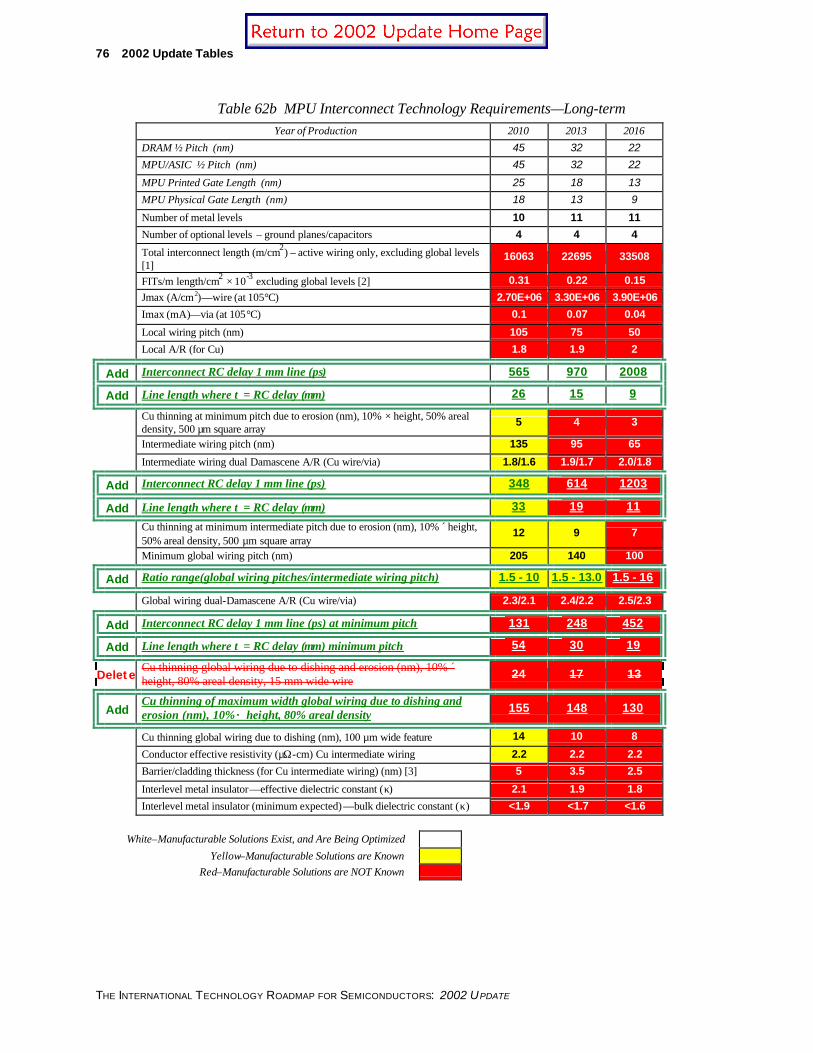
76 2002 Update Tables
THE INTERNATIONAL TECHNOLOGY ROADMAP FOR SEMICONDUCTORS: 2002 UPDATE
Table 62b MPU Interconnect Technology Requirements—Long-term Year of Production 2010 2013 2016
DRAM ½ Pitch (nm) 45 32 22
MPU/ASIC ½ Pitch (nm) 45 32 22
MPU Printed Gate Length (nm) 25 18 13
MPU Physical Gate Length (nm) 18 13 9
Number of metal levels 10 11 11
Number of optional levels – ground planes/capacitors 4 4 4
Total interconnect length (m/cm2) – active wiring only, excluding global levels [1]
16063 22695 33508
FITs/m length/cm2 × 10-3 excluding global levels [2] 0.31 0.22 0.15
Jmax (A/cm2)—wire (at 105°C) 2.70E+06 3.30E+06 3.90E+06
Imax (mA)—via (at 105°C) 0.1 0.07 0.04
Local wiring pitch (nm) 105 75 50
Local A/R (for Cu) 1.8 1.9 2
Add Interconnect RC delay 1 mm line (ps) 565 970 2008
Add Line length where τ = RC delay (µm) 26 15 9
Cu thinning at minimum pitch due to erosion (nm), 10% × height, 50% areal density, 500 µm square array
5 4 3
Intermediate wiring pitch (nm) 135 95 65
Intermediate wiring dual Damascene A/R (Cu wire/via) 1.8/1.6 1.9/1.7 2.0/1.8
Add Interconnect RC delay 1 mm line (ps) 348 614 1203
Add Line length where τ = RC delay (µm) 33 19 11
Cu thinning at minimum intermediate pitch due to erosion (nm), 10% ´ height, 50% areal density, 500 µm square array
12 9 7
Minimum global wiring pitch (nm) 205 140 100
Add Ratio range(global wiring pitches/intermediate wiring pitch) 1.5 - 10 1.5 - 13.0 1.5 - 16
Global wiring dual-Damascene A/R (Cu wire/via) 2.3/2.1 2.4/2.2 2.5/2.3
Add Interconnect RC delay 1 mm line (ps) at minimum pitch 131 248 452
Add Line length where τ = RC delay (µm) minimum pitch 54 30 19
Delete Cu thinning global wiring due to dishing and erosion (nm), 10% ´ height, 80% areal density, 15 mm wide wire 24 17 13
Add Cu thinning of maximum width global wiring due to dishing and erosion (nm), 10% × height, 80% areal density 155 148 130
Cu thinning global wiring due to dishing (nm), 100 µm wide feature 14 10 8
Conductor effective resistivity (µΩ-cm) Cu intermediate wiring 2.2 2.2 2.2
Barrier/cladding thickness (for Cu intermediate wiring) (nm) [3] 5 3.5 2.5
Interlevel metal insulator—effective dielectric constant (κ) 2.1 1.9 1.8
Interlevel metal insulator (minimum expected) —bulk dielectric constant (κ) <1.9 <1.7 <1.6
White–Manufacturable Solutions Exist, and Are Being Optimized
Yellow–Manufacturable Solutions are Known
Red–Manufacturable Solutions are NOT Known

2002 Update Tables 77
THE INTERNATIONAL TECHNOLOGY ROADMAP FOR SEMICONDUCTORS: 2002 UPDATE
Table 63a DRAM Interconnect Technology Requirements—Near-term
Year of Production 2001 2002 2003 2004 2005 2006 2007
DRAM ½ Pitch (nm) 130 115 100 90 80 70 65
MPU/ASIC ½ Pitch (nm) 150 130 107 90 80 70 65
MPU Printed Gate Length (nm) 90 75 65 53 45 40 35
MPU Physical Gate Length (nm) 65 53 45 37 32 28 25
Number of metal levels 3 3–4 4 4 4 4 4
Was Contact A/R—stacked capacitor 11.4 11.9 12.4 13 13.6 14.3 15.2
Is Contact A/R—stacked capacitor 11 12 13 15 15 16 16
Local wiring pitch (nm) non-contacted 260 230 200 180 160 150 130
Was Specific contact resistance (Ω-cm2) 1.50E-07 1.30E-07 1.00E-07 8.00E-08 7.00E-08 6.00E-08 5.00E-08
Is Specific contact resistance (Ω-cm2) 1.7E-07 1.4E-07 1.0E-07 8.5E-08 7.0E-08 5.0E-08 4.0E-08
Was Specific via resistance (Ω-cm2) 2.00E-09 1.40E-09 1.00E-09 9.00E-10 7.00E-10 6.00E-10 5.00E-10
Is Specific via resistance (Ω-cm2) 2.0E-09 1.5E-09 1.1E-09 9.0E-10 7.5E-10 5.8E-10 5.0E-10
Conductor effective resistivity (µΩ-cm) 3.3 3.3 3.3 2.2 2.2 2.2 2.2
Interlevel metal insulator—effective dielectric constant (κ)
4.1 3.0–4.1 3.0–4.1 3.0–4.1 3.0-4.1 2.6–3.1 2.6–3.1
White–Manufacturable Solutions Exist, and Are Being Optimized
Yellow–Manufacturable Solutions are Known
Red–Manufacturable Solutions are NOT Known
Notes for Table 62a and b
[1] Calculated by assuming that only one of every three minimum pitch wiring tracks for local and semiglobal wiring levels are populated. The wiring lengths for each level are then summed to calculate the total interconnect length per square centimeter of active area.
[2] This metric is calculated by assuming that a 5 FIT reliability budget is apportioned to interconnect for the highest reliability grade MPUs. This number is then divided by the total interconnect length to arrive at the FITs per meter of wiring per one square centimeter of active area.
[3] Calculated for a conformal layer in intermediate wiring to meet minimum effective conductor resistivity

78 2002 Update Tables
THE INTERNATIONAL TECHNOLOGY ROADMAP FOR SEMICONDUCTORS: 2002 UPDATE
Table 63b DRAM Interconnect Technology Requirements—Long-term
Year of Production 2010 2013 2016
DRAM ½ Pitch (nm) 45 32 22
MPU/ASIC ½ Pitch (nm) 45 32 22
MPU Printed Gate Length (nm) 25 18 13
MPU Physical Gate Length (nm) 18 13 9
Number of metal levels 4 4 4
Was Contact A/R—stacked capacitor 16.1 19.3 23.2
Is Contact A/R—stacked capacitor > 20 > 20 > 20
Local wiring pitch (nm) non-contacted 90 64 44
Was Specific contact resistance (Ω-cm2) 4.00E-08 2.00E-08 1.00E-08
Is Specific contact resistance (Ω-cm2) 2.3E-08 1.2E-08 5.5E-09
Was Specific via resistance (Ω-cm2) 5.00E-10 3.00E-10 1.00E-10
Is Specific via resistance (Ω-cm2) 3.2E-10 1.6E-10 7.6E-11
Conductor effective resistivity (µΩ-cm) 2.2 2.2 2.2
Interlevel metal insulator—effective dielectric constant (κ) 2.3–2.7 2.3–2.7 2.1
White–Manufacturable Solutions Exist, and Are Being Optimized Yellow–Manufacturable Solutions are Known
Red–Manufacturable Solutions are NOT Known

2002 Update Tables 79
THE INTERNATIONAL TECHNOLOGY ROADMAP FOR SEMICONDUCTORS: 2002 UPDATE
FACTORY INTEGRATION Table 65 Factory Integration Difficult Challenges [Update]
Difficult Challenges ≥ 65 nm, Through 2007
Summary of Issues
Was Complexity Management • Rapid changes to business needs, demand, and globalization trends • Increasing rate of new product and technology introductions • Globally disparate factories run as single “virtual factory” • Need to meet regulations in different geographical areas • Effectively manage complex supply chains • Increasing process and product complexity • Explosive growth of data collection/analysis requirements • Increasing number of processing steps including material movements • Multiple lots in a carrier and single wafer control/transport for an equipment group • Multiple Products on a wafer • Multiple package form factors • Larger wafers and carriers driving ergonomic solutions • Increasing expectations for integrated material handling and software control systems • Increased reliance on factory information and control systems • Multiple information and control sy stem interdependencies • Standalone and Integrated Reliability required to keep factories operating • Co-existence of new factory information and control systems with existing (legacy) systems • Pace of standards definition and implementation is not meeting factory integration needs • Addressing complexity while keeping costs in perspective
Is Complexity Management • Rapid changes to business needs, demand, and globalization trends • Increasing rate of new product and technology introductions • Globally disparate factories run as single “virtual factory” • Need to meet regulations in different geographical areas • Effectively manage complex supply chains • Increasing process and product complexity • Increasing number of processing steps including material movements • Multiple lots in a carrier and single wafer control/transport for an equipment group • Multiple Products on a wafer and multiple package form factors • Increasing expectations for integrated material handling and software control systems • Increased reliance on factory information and control systems • Multiple information and control system interdependencies • Standalone and Integrated Reliability required to keep factories operating • Co-existence of new factory information and control systems with existing systems • Pace of standards definition and implementation is not meeting needs • Addressing complexity while keeping costs in perspective • Explosive growth of data collection/analysis requirements driven by process and modeling needs • Need to meet technology restrictions with some countries while still meeting business needs
Was Factory Optimization • Increased customer expectation to meet on time delivery • Balanced throughput and cycle time • Reduce time to ramp factories, products, and processes • Increased urgency for improved factory effectiveness • Ability to measure effectiveness and adjust/optimize factory output • High factory yield at startup • Reduce effects of parametric variation • Reduce wafer and product cost • Satisfy all domestic and international regulations
Is Factory Optimization • Increased customer expectation to meet on time delivery • Balanced throughput and cycle time • Reduce time to ramp factories, products, and processes • Ability to measure effectiveness and adjust/optimize factory output • High factory yield at startup • Reduce effects of parametric variation • Reduce wafer and product cost • Satisfy all domestic and international regulations • Customer expectation for faster new product and volume deliveries • Improving both throughput and cycle time

80 2002 Update Tables
THE INTERNATIONAL TECHNOLOGY ROADMAP FOR SEMICONDUCTORS: 2002 UPDATE
Table 65 Factory Integration Difficult Challenges [Update](continued)
Extendibility, Flexibility, and Scalability
• Reuse of building, production and support equipment, and factory information and control sy stems across multiple technology nodes and wafer size conversions • Factory designs that support rapid process and technology changes and retrofits • Understand up-front costs to incorporate EFS • Determine which EFS features to include and not to include • Minimize downtime to on-going operations • Comprehend tighter ESH/Code requirements • Comprehend increased purity requirements for process and materials
Difficult Challenges ≥ 65 nm, Through 2007
Summary of Issues
Was Post Bulk CMOS Manufacturing
• New devices beyond traditional bulk CMOS will drive significant changes in process technology and the factory manufacturing capabilities to support it • New production equipment must be designed and integrated with the factory • Yield and process control capabilities must be modified to new device process technology needs • Unknown changes to factory operations motivated by new device change • Potential for additional process and functional area isolation • Need to run CMOS and post CMOS processes within the same factory • Rapid technology development and ramp to support high volume manufacturing of new devices • Continued pressure to maintain 0.7× shrink per year efficiency in equivalent die size • Development and high volume ramp timeline must meet current technology node shrinks goals • Device yield and factory output must meet current roadmap targets • Reuse of buildings and equipment to enable new device technology at an affordable cost • Potential for additional process and functional area isolation an • Need to run CMOS and post CMOS processes within the same factory • Comprehend tighter ESH and code requirements
Is Post Bulk CMOS Manufacturing
• Identifying and implementing the new device manufacturing capabilities beyond bulk CMOS in time for a low risk industry transition • New production equipment must be designed and integrated with the factory • Yield and process control capabilities must be modified to new device process technology needs • Unknown changes to factory operations motivated by new device change • Potential for additional process and functional area isolation • Need to run CMOS and post CMOS processes within the same factory • Rapid technology development and ramp to support high volume manufacturing of new devices • Continued pressure to maintain 0.7× shrink per year efficiency in equivalent die size • Development and high volume ramp timeline must meet current technology node shrinks goals • Device yield and factory output must meet current roadmap targets • Reuse of buildings and equipment to enable new device technology at an affordable cost • Potential for additional process and functional area isolation an • Need to run CMOS and post CMOS processes within the same factory • Comprehend tighter ESH and code requirements
Was 450 mm Wafer Size Conversion
• Larger wafers and carriers driving changes to traditional wafer size scale-up strategy • Increased requirements for wafer level integration within the factory • Significant changes to production equipment and material handling design • Pressure to met affordability targets • Reuse of buildings and equipment to enable 450 mm at an affordable cost • Comprehend tighter ESH and code requirements
Is 450 mm Wafer Size Conversion
• Larger wafers and carriers driving changes to traditional wafer size scale-up strategy • Increased requirements for wafer level integration within the factory • Significant changes to production equipment and material handling design • Pressure to met affordability targets • Reuse of buildings and equipment to enable 450 mm at an affordable cost • Comprehend tighter ESH and code requirements

2002 Update Tables 81
THE INTERNATIONAL TECHNOLOGY ROADMAP FOR SEMICONDUCTORS: 2002 UPDATE
Table 66a Factory Operations Technology Requirements—Near-term Year of Production 2001 2002 2003 2004 2005 2006 2007
DRAM ½ Pitch (nm) 130 115 100 90 80 70 65
MPU / ASIC ½ Pitch (nm) 150 130 107 90 80 70 65
MPU Printed Gate Length (nm) 90 75 650 53 45 40 35
MPU Physical Gate Length (nm) 65 53 45 37 32 28 25
Wafer Diameter 300 mm 300 mm 300 mm 300 mm 300 mm 300 mm 300 mm
High Volume / Low Mix Factory Requirements [4, 5]
Was Factory cycle time per mask layer (non-hot lot) [1,2] (days) 1.4 1.4 1.4 1.3 1.3 1.3 1.2
Is Factory cycle time per mask layer (non-hot lot) [1,2] (days) 1.4 1.4 1.4 1.3 1.3 1.3 1.2
Was Factory cycle time per mask layer (hot lot) [1,2,7] (days) 1 1 1 0.9 0.9 0.9 0.8
Is Factory cycle time per mask layer (hot lot) [1,2,7] (days) 1 1 1 0.9 0.9 0.9 0.8
Number of lots per carrier (lot) One One One One One One One
Was Wafer layers/day/head count 55 55 55 61 61 61 67
Is Wafer layers/day/head count 55 55 55 61 61 61 67
High Volume / High Mix Factory Requirements [4, 5, 6]
Was Factory cycle time per mask layer (non-hot lot) [2,3] (days) 1.2 1.2 1.2 1.1 1.1 1.1 1
Is Factory cycle time per mask layer (non-hot lot) [2,3] (days) 1.2 1.2 1.2 1.1 1.1 1.1 1
Was Factory cycle time per mask layer (hot lot) [2,3,7] (days) 0.75 0.75 0.75 0.65 0.65 0.65 0.55
Is Factory cycle time per mask layer (hot lot) [2,3,7] (days) 0.75 0.6 0.6 0.55 0.5 0.45 0.4
Number of lots per carrier (lot) Multiple Multiple Multiple Multiple Multiple Multiple Multiple
Wafer layers/day/head count 37 37 37 41 41 41 45
Common requirements across Both Factory Types
Was Groundbreaking to first tool move-in (months) 9 9 9 8 8 8 7
Is Groundbreaking to first tool move-in (months). 9 9 9 8 8 8 7
First tool move-in to first full loop wafer out (months) 4 3.5 3.5 3 3 2.5 2.5
Was Node to Node change-over (weeks) 13 13 13 12 12 12 11
Is Node to Node change-over (weeks) 13 13 13 12 12 12 11
Floor space effectiveness 1X 1X 1X 1X 1X 1X 1X
White–Manufacturable Solutions Exist, and Are Being Optimized
Yellow–Manufacturable Solutions are Known
Red–Manufacturable Solutions are NOT Known

82 2002 Update Tables
THE INTERNATIONAL TECHNOLOGY ROADMAP FOR SEMICONDUCTORS: 2002 UPDATE
Table 66b Factory Operations Technology Requirements—Long-term
Year of Production 2010 2013 2016
DRAM ½ Pitch (nm) 45 32 22
MPU / ASIC ½ Pitch (nm) 45 32 22
MPU Printed Gate Length (nm) 25 18 13
MPU Physical Gate Length (nm) 18 13 9
Wafer Diameter 300 mm 450 mm 450 mm
High Volume / Low Mix Factory Requirements [4, 5]
Factory cycle time per mask layer (non-hot lot) [1,2] (days) 1.1 1.05 1
Factory cycle time per mask layer (hot lot) [1,2,7] (days) 0.7 0.65 0.6
Number of lots per carrier (lot) One One One
Wafer layers/day/head count 73 81 89
High Volume / High Mix Factory Requirements [4, 5, 6]
Factory cycle time per mask layer (non-hot lot) [2,3] (days) 0.9 0.95 0.8
Factory cycle time per mask layer (hot lot) [2,3,7] (days) 0.45 0.4 0.35
Number of lots per carrier (lot) Multiple Multiple Multiple
Wafer layers/day/head count 49 54 60
Common requirements across Both Factory Types
Groundbreaking to first tool move-in (months) 6 5.5 5
First tool move-in to first full loop wafer out (months) 2 1.5 1
Node to Node change-over (weeks) 10 9.5 9
Floor space effectiveness 1X 1X 1X
White–Manufacturable Solutions Exist, and Are Being Optimized
Yellow–Manufacturable Solutions are Known
Red–Manufacturable Solutions are NOT Known

2002 Update Tables 83
THE INTERNATIONAL TECHNOLOGY ROADMAP FOR SEMICONDUCTORS: 2002 UPDATE
Explanation of Items for Factory Operations Technology Requirements:
Item Explanation
Factory cycle time per mask layer (non-hot lot) [1,2]
Assume 25 (variable) wafers per lot. For example, if a process has 20 masking layers, and cycle time per mask layer is 1.5, then total factory (fabrication) cycle time is 20x1.5 = 30 days. A key metric of time to money.
Factory cycle time per mask layer (hot lot) [1,2,7]
Same definition as of above. Factories typically prioritize these lots over conventional lots, sometimes hold tools downstream to rapidly move them through the process flow and may also reduce metrology steps and sampling rates. As a result, the cycle time for hot lots are < 50% of non-hot lots. Assume 5-10 wafers per lot.
Was Number of lots per carrier Number of lots in each carrier that needs to be tracked, monitored, and processed at each production equipment. It impacts the extent of "recipe cascading" which enables production equipment to run in a continuous (non-stop) mode between lots in the same carrier and between sequential carriers.
Is Number of lots per carrier The number of lots in each carrier that need to be tracked, monitored, and processed. For high mix factories, the number of lots < 25 and the production equipment must be able to run a different recipe and/or parameters for each wafer within the carrier. It also requires the Factory Information and Control system to be able to track, monitor, and control the wafer at each point the factory and within the equipment. The Factory Information and control system must have the ability to drive the production equipment to run different recipes and/or parameters for each wafer.
Wafer layers/day/head count Measure of productivity which includes equipment output and direct labor staffing .Equation = total wafer processed per day in the factory x # of litho mask layers/total # of direct labor employees per day.
Groundbreaking to first full tool move-in Time in months measured from groundbreaking to first move-in to the fab. Assumes site availability and all contract permits approved
First tool move-in to first full loop wafer out
A key metric of new factory ramp-up time. This is the time elapsed in months from first tool move-in to first full loop wafer out.
Node to Node change-over time The time in weeks for a new product or process to be implemented in a working factory (production equipment move-in to first lot out). About 80% of the current equipment is reused and 20% is new. Equipment already in place or available and may need to be qualified. Furnace and wet process equipment are not replaced. Not serial #1 equipment.
Floor space effectiveness This is a measure of equipment installation density in the cleanroom, and drives the requirement for the smallest footprint and the fastest run rate for production equipment. Equation = (# of Processing steps in the fab * WSPM/(Floor space area*30days). For every major node, one additional metal layer is added, and assuming a 4% increased run-rate improvement each year (by reduced processing time per wafer), the best that can be mathematically achieved is getting the same output per sq. meters of cleanroom for each new node.
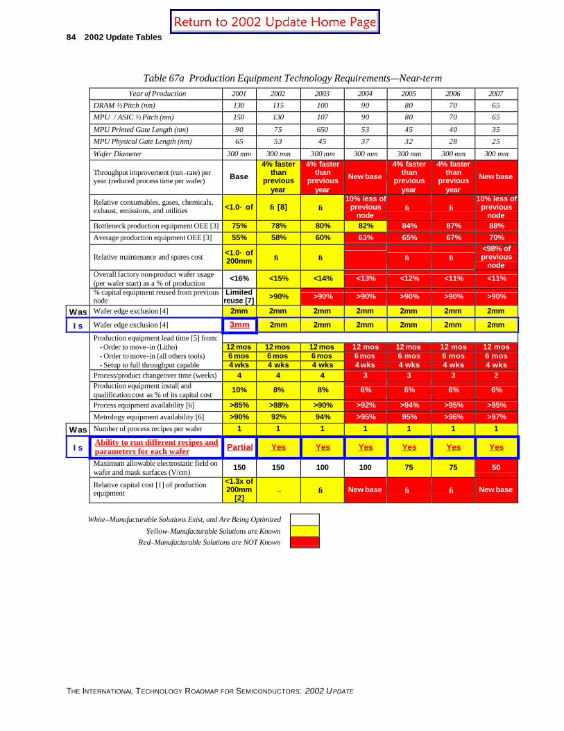
84 2002 Update Tables
THE INTERNATIONAL TECHNOLOGY ROADMAP FOR SEMICONDUCTORS: 2002 UPDATE
Table 67a Production Equipment Technology Requirements—Near-term Year of Production 2001 2002 2003 2004 2005 2006 2007
DRAM ½ Pitch (nm) 130 115 100 90 80 70 65
MPU / ASIC ½ Pitch (nm) 150 130 107 90 80 70 65
MPU Printed Gate Length (nm) 90 75 650 53 45 40 35
MPU Physical Gate Length (nm) 65 53 45 37 32 28 25
Wafer Diameter 300 mm 300 mm 300 mm 300 mm 300 mm 300 mm 300 mm
Throughput improvement (run -rate) per year (reduced process time per wafer) Base
4% faster than
previous year
4% faster than
previous year
New base
4% faster than
previous year
4% faster than
previous year
New base
Relative consumables, gases, chemicals, exhaust, emissions, and utilities <1.0× of →[8] →
10% less of previous
node → →
10% less of previous
node
Bottleneck production equipment OEE [3] 75% 78% 80% 82% 84% 87% 88%
Average production equipment OEE [3] 55% 58% 60% 63% 65% 67% 70%
Relative maintenance and spares cost <1.0× of 200mm → → → →
<98% of previous
node
Overall factory non-product wafer usage (per wafer start) as a % of production
<16% <15% <14% <13% <12% <11% <11%
% capital equipment reused from previous node
Limited reuse [7] >90% >90% >90% >90% >90% >90%
Was Wafer edge exclusion [4] 2mm 2mm 2mm 2mm 2mm 2mm 2mm
Is Wafer edge exclusion [4] 3mm 2mm 2mm 2mm 2mm 2mm 2mm
Production equipment lead time [5] from: - Order to move-in (Litho) 12 mos 12 mos 12 mos 12 mos 12 mos 12 mos 12 mos - Order to move-in (all others tools) 6 mos 6 mos 6 mos 6 mos 6 mos 6 mos 6 mos
- Setup to full throughput capable 4 wks 4 wks 4 wks 4 wks 4 wks 4 wks 4 wks
Process/product changeover time (weeks) 4 4 4 3 3 3 2
Production equipment install and qualification cost as % of its capital cost
10% 8% 8% 6% 6% 6% 6%
Process equipment availability [6] >85% >88% >90% >92% >94% >95% >95%
Metrology equipment availability [6] >90% 92% 94% >95% 95% >96% >97%
Was Number of process recipes per wafer 1 1 1 1 1 1 1
Is Ability to run different recipes and parameters for each wafer Partial Yes Yes Yes Yes Yes Yes
Maximum allowable electrostatic field on wafer and mask surfaces (V/cm)
150 150 100 100 75 75 50
Relative capital cost [1] of production equipment
<1.3x of 200mm
[2] → → New base → → New base
White–Manufacturable Solutions Exist, and Are Being Optimized
Yellow–Manufacturable Solutions are Known
Red–Manufacturable Solutions are NOT Known

2002 Update Tables 85
THE INTERNATIONAL TECHNOLOGY ROADMAP FOR SEMICONDUCTORS: 2002 UPDATE
Table 67b Production Equipment Technology Requirements—Long-term Year of Production 2010 2013 2016
DRAM ½ Pitch (nm) 45 32 22
MPU / ASIC ½ Pitch (nm) 45 32 22
MPU Printed Gate Length (nm) 25 18 13
MPU Physical Gate Length (nm) 18 13 9
Wafer Diameter 300 mm 450 mm 450 mm
Throughput improvement (run -rate) per year (reduced process time per wafer)
10–12% faster than previous node
10–12% faster than previous node
10–12% faster than previous node
Relative consumables, gases, chemicals, exhaust, emissions, and utilities
10% less than previous node
10% less than previous node
10% less than previous node
Bottleneck production equipment OEE [3] 90% 91% 92%
Average production equipment OEE [3] 72% 74% 75%
Relative maintenance and spares cost <98% of previous node <120% of previous node <98% of previous node
Overall factory non-product wafer usage (per wafer start) as a % of production
<10% <9% <9%
% capital equipment reused from previous node >70% Limited reuse [7] >70%
Wafer edge exclusion [4] 2mm 2mm 2mm Production equipment lead time [5] from: - Order to move-in (Litho) 12 mos 12 mos 12 mos - Order to move-in (all others tools) 6 mos 6 mos 6 mos - Setup to full throughput capable 4 wks 4 wks 4 wks
Process/product changeover time (weeks) 2 2 2
Production equipment install and qualification cost as % of its capital cost 6% 8% 6%
Process equipment availability [6] >95% >95% >95%
Metrology equipment availability [6] >98% >98% >98%
Was Number of process recipes per wafer 1 1 1
Is Ability to run different recipes and parameters for each wafer Yes Yes Yes
Maximum allowable electrostatic field on wafer and mask surfaces (V/cm) 50 25 25
Relative capital cost [1] of production equipment New base <1.3x of 300 mm New base
White–Manufacturable Solutions Exist, and Are Being Optimized
Yellow–Manufacturable Solutions are Known
Red–Manufacturable Solutions are NOT Known

86 2002 Update Tables
THE INTERNATIONAL TECHNOLOGY ROADMAP FOR SEMICONDUCTORS: 2002 UPDATE
Explanation of Items for Production Equipment Requirements
Item Explanation
Target throughput improvement (run-rate) per year (or reduced processing time per wafer)
Throughput improvements are achieved by reducing the processing time per wafer, and optimizing non-value added wafer handling and wafer-staging steps inside the equipment and by increasing the efficiency of the equipment embedded controller. Also eliminate any dead time between sequential wafer processing steps. E.g.,: if current run-rate is 100 wafers/hour, the required run-rate next year is (100 x 1.04) = 104 wafers/hour and (104 x 1.04)=108 wafers/hour the following year.
Relative consumables, exhaust, emissions, and utilities
For the 130 nm node, relative consumables are a ratio of (300 mm consumables/300 mm throughput in wafers per hour) divided by (200 mm consumables/200 mm throughput in wafers per hour). The same methodology applies for gases, chemicals, exhaust, emissions, and utilities. For the 90 nm node and beyond consumables is 90% of previous node assuming the same throughput. Global warming and general ESH initiatives may force additional tightening of this requirement.
Bottleneck production equipment OEE
Overall equipment efficiency of the bottleneck production equipment. (Refer to SEMI E79 for OEE definition.) Bottleneck refers to the most constraint (limiting output) equipment in the factory.
Average production equipment OEE
Overall equipment efficiency of the average production equipment. (Refer to SEMI E79 for OEE definition.)
Relative equipment footprint
For the 130 nm node, it is ratio of (300 mm equipment footprint/300 mm throughput in wafers per hour) divided by (200 mm equipment footprint/200 mm throughput in wafers per hour). For the 90 nm node and beyond, footprint is 98% of previous node assuming the same throughput. [ Refer to SEMI E72. 1 The footprint used here infers to th e cost footprint in the SEMI standard.]
Relative maintenance and spares cost
For the 130 nm node, it is ratio of (300 mm maintenance and spares cost/300 mm throughput in wafers per hour) divided by (200 mm maintenance and spares cost/200 mm throughput in wafers per hour). For the 90 nm node and beyond it is 98% of previous node assuming the same throughput.
Overall factory non-product wafer usage (per wafer start)
Ratio of total non-production wafer consumption divided by total production wafer started for the same period. Typical non-product wafers include test wafers, monitor wafers, calibration wafers, dummy wafers. Consumption quantity includes both new and reused (reclaimed) non-product wafers.
% Capital equipment reused from previous technology node
% of capital (production) equipment quantity that is reused from node N to N+1. Example: if X number of production equipment of node N can be reused for node N+1 and the total number of production equipment for node N+1 is Y, then equipment reuse % is defined as X/Y.
Wafer edge exclusion
Dimension in millimeters measured from wafer edge that is not used for printing saleable chips. Includes front and rear sides of wafer.
Production equipment lead time
Time elapsed between when a purchase order has been placed for production equipment till the time the equipment has been qualified to run wafers at the quoted throughput (wafers per hour). Assume it is repeat order equipment, suppliers have sufficient mfg capacity, and learning achieved for fast install/qualification. For tools with long-lead items, risk reduction for equipment suppliers from order cancellation exposure may be mitigated by creative down-payment schemes.
Process/Product changeover time (in weeks)
Total time elapsed for old equipment move-out, new equipment move-in, install/hook-up and supplier qualification complete. Also assumes new equipment has space to move-in and major utility laterals are in place. Assume same wafer size, factory does not shut down and > 90% of existing equipment is reused.
Production equipment install & qualification cost as a % of capital equipment cost
Ratio of production equipment (installation cost + hook-up cost + qualification cost) divided by its upfront capital cost, expressed as a percentage. Equipment and facilities hook-up standardization will reduce this cost.
Process equipment availability
Availability is 100% minus (scheduled downtime % + unscheduled downtime %) of the process (non-metrology) equipment. Scheduled downtime and unscheduled downtimes are defined in SEMI E10.
Metrology equipment availability
Availability is 100% minus (scheduled downtime % + unscheduled downtime %) of the metrology equipment. Scheduled downtime and unscheduled downtimes are defined in SEMI E10.
1 SEMI. E72-0699 – Provisional Specification and Guide for 300 mm Equipment Footprint, Height, and Weight .
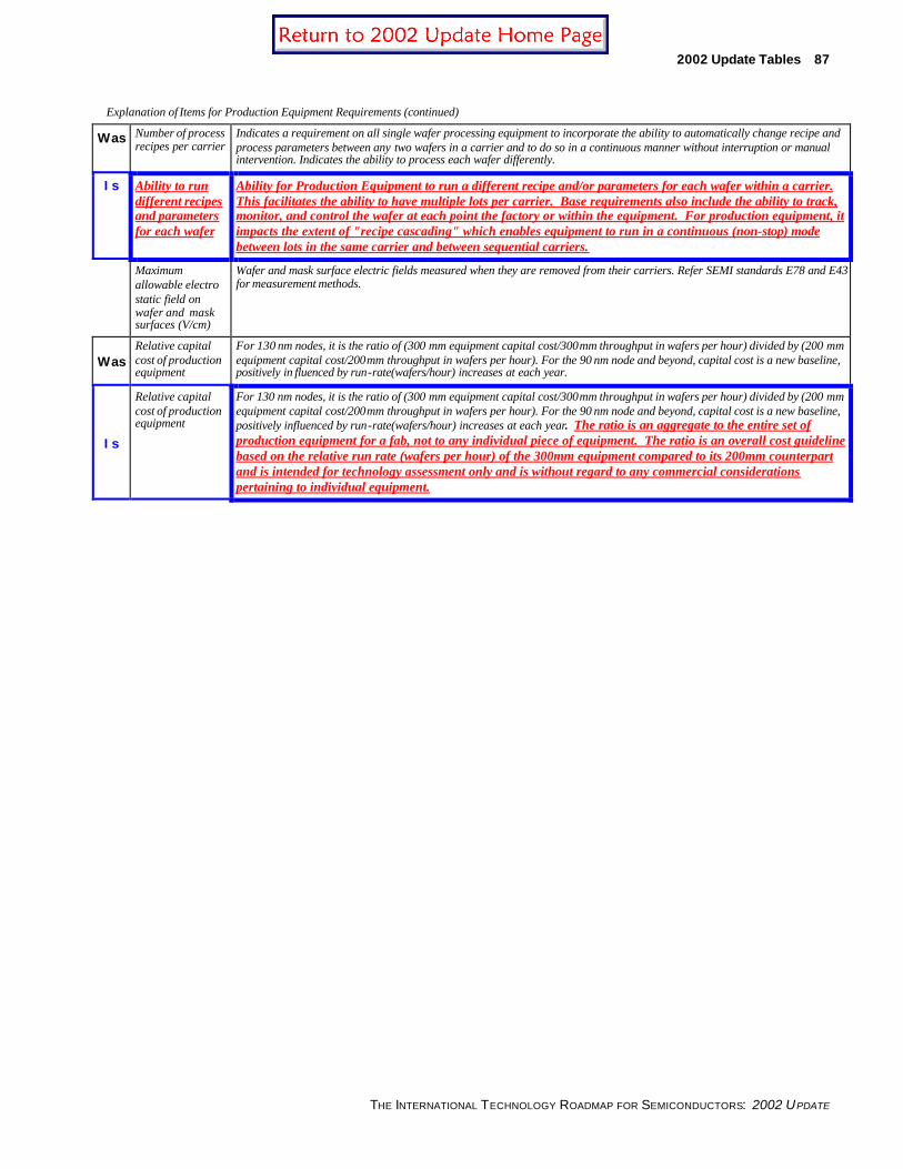
2002 Update Tables 87
THE INTERNATIONAL TECHNOLOGY ROADMAP FOR SEMICONDUCTORS: 2002 UPDATE
Explanation of Items for Production Equipment Requirements (continued)
Was Number of process recipes per carrier
Indicates a requirement on all single wafer processing equipment to incorporate the ability to automatically change recipe and process parameters between any two wafers in a carrier and to do so in a continuous manner without interruption or manual intervention. Indicates the ability to process each wafer differently.
Is Ability to run different recipes and parameters for each wafer
Ability for Production Equipment to run a different recipe and/or parameters for each wafer within a carrier. This facilitates the ability to have multiple lots per carrier. Base requirements also include the ability to track, monitor, and control the wafer at each point the factory or within the equipment. For production equipment, it impacts the extent of "recipe cascading" which enables equipment to run in a continuous (non-stop) mode between lots in the same carrier and between sequential carriers.
Maximum allowable electro static field on wafer and mask surfaces (V/cm)
Wafer and mask surface electric fields measured when they are removed from their carriers. Refer SEMI standards E78 and E43 for measurement methods.
Was Relative capital cost of production equipment
For 130 nm nodes, it is the ratio of (300 mm equipment capital cost/300 mm throughput in wafers per hour) divided by (200 mm equipment capital cost/200 mm throughput in wafers per hour). For the 90 nm node and beyond, capital cost is a new baseline, positively in fluenced by run-rate(wafers/hour) increases at each year.
Is
Relative capital cost of production equipment
For 130 nm nodes, it is the ratio of (300 mm equipment capital cost/300 mm throughput in wafers per hour) divided by (200 mm equipment capital cost/200 mm throughput in wafers per hour). For the 90 nm node and beyond, capital cost is a new baseline, positively influenced by run-rate(wafers/hour) increases at each year. The ratio is an aggregate to the entire set of production equipment for a fab, not to any individual piece of equipment. The ratio is an overall cost guideline based on the relative run rate (wafers per hour) of the 300mm equipment compared to its 200mm counterpart and is intended for technology assessment only and is without regard to any commercial considerations pertaining to individual equipment.

88 2002 Update Tables
THE INTERNATIONAL TECHNOLOGY ROADMAP FOR SEMICONDUCTORS: 2002 UPDATE
Table 68a Material Handling Systems Technology Requirements—Near-term (40K WSPM*) [7]
Year of Production 2001 2002 2003 2004 2005 2006 2007
DRAM ½ Pitch (nm) 130 115 100 90 80 70 65
MPU / ASIC ½ Pitch (nm) 150 130 107 90 80 70 65
MPU Printed Gate Length (nm) 90 75 650 53 45 40 35
MPU Physical Gate Length (nm) 65 53 45 37 32 28 25
Material handling total capital cost as a % of total capital cost < 3% [1] < 3% < 3% < 2% [2] < 2% < 2% < 2%
Was # Of transport system types within a factory 2 [3] 2 2 Some 1 and
some 2 1 [4] 1 1
Is Wafer Transport system capability
Separate interbay & intrabay
Separate interbay
& intrabay
Separate interbay & intrabay
Some interbay & intrabay,
Some Direct tool to
tool
Direct tool to
tool
Direct tool to
tool
Direct tool to
tool
Was MTTR (minutes) (SEMI E10) 4 20 18 15 15 15 15
Is MTTR (minutes) (SEMI E10) 24 20 18 15 15 15 15
Failures per 24-hour day over total system (SEMI E10)
<1 <1 <0.75 <0.5 <0.5 <0.5 <0.5
System throughput
Was • Interbay transport (moves/hour)
1200 1300 1400 1500 1625 [4] 1750 1875
Is • Interbay transport (moves/hour) [40K WSPM] 2400 2600 2800 3000 3250 [4] 3500 3750
Was • Intrabay transport (moves/hour) 170 180 190 200 1625 [4] 1750 1875
Is • Intrabay transport (moves/hour) [40K WSPM] 170 180 190 200 3250 [4] 3500 3750
Stocker cycle time (seconds) 15 15 14 12 12 10 10
Average factory wide carrier delivery time (in minutes) 10 10 10 8 5 5 5
Maximum factory wide carrier delivery time 20 20 20 15 15 15 15
Stocker storage density (% Total WIP
carrier volume / Total stocker volume) [5]
Small stocker (%) > 25 >30 >30 >40 >40 >40 >50
Nominal stocker (%) >30 >35 >35 >45 >50 >50 >60
Was Material handling equipment lead time (weeks)
<16 <14 <12 <11 <10 <9 <8
Is Material handling equipment lead time (weeks) <16 <14 <12 <11 <10 <9 <8
Material handling equipment installation time (weeks)
<8 <8 <7 <7 <6 <5 <4
Was System downtime required to extend system capacity when previously planned (minutes) [6]
<180 <90 <90 <60 <30 <30 <15
Is System downtime required to extend system capacity when previously planned (minutes) [6]
<180 <90 <90 <60 <30 <30 <15
Add *WSPM—wafer starts per month White–Manufacturable Solutions Exist, and Are Being Optimized
Yellow–Manufacturable Solutions are Known
Red–Manufacturable Solutions are NOT Known

2002 Update Tables 89
THE INTERNATIONAL TECHNOLOGY ROADMAP FOR SEMICONDUCTORS: 2002 UPDATE
Table 68b Material Handling Systems Technology Requirements—Long-term (40K WSPM*) [7] Year of Production 2010 2013 2016
DRAM ½ Pitch (nm) 45 32 22
MPU / ASIC ½ Pitch (nm) 45 32 22
MPU Printed Gate Length (nm) 25 18 13
MPU Physical Gate Length (nm) 18 13 9
Wafer Diameter 300 mm 450 mm 450 mm
Material handling total capital cost as a % of total capital cost < 2% < 3% < 3%
Was # Of transport system types within a factory 1 1 1
Is Wafer Transport system capability Direct tool to tool Direct tool to tool Direct tool to tool
MTTR (minutes) (SEMI E10) 12 10 8
Failures per 24-hour day over total system (SEMI E10)
<0.5 <0.5 <0.3
Was System throughput
• Interbay transport (moves/hour)
• Intrabay transport (moves/hour) 2000 2000 2000
Is System throughput
• Interbay transport (moves/hour) [40K WSPM]
• Intrabay transport (moves/hour) [40K WSPM] 4000 4000 4000
Stocker cycle time (seconds) 8 10 10
Average factory wide carrier delivery time (in minutes) 5 5 5
Maximum factory wide carrier delivery time 12 10 8
Stocker storage density (% Total WIP carrier volume / Total stocker volume) [5]
Small stocker (%) >50 >50 >50
Nominal stocker (%) >60 >60 >60
Material handling equipment lead time (weeks) <8 <8 <8
Material handling equipment installation time (weeks) <4 <4 <4
System downtime required to extend system capacity when previously planned (minutes) [6]
30 30 30
Add *WSPM—wafer starts per month White–Manufacturable Solutions Exist, and Are Being Optimized
Yellow–Manufacturable Solutions are Known
Red–Manufacturable Solutions are NOT Known
Notes for Material Handling Systems Technology Requirements Tables:
[1] Year 2002—High throughput transportation
[2] Year 2005—Ability for Direct tool-to tool-delivery Direct transportation and fewer stockers
[3] Interbay and intrabay transport system types
[4] Single direct transport system Transport system capable of achieving factory wide direct tool-to-tool delivery
[5] Required external maintenance access space is not included in these values. However, it is expected that required maintenance access, except for electrical power distribution access on the back, should be designed for internal to the stocker, with the proper clearance for entering/exiting the stocker.
[6] These values are do not include downtimes associated with software upgrades, which are addressed by the Factory Information and Control Systems requirements (see Table 55) for unavailability of a mission critical application in a working factory due to install/upgrade (minutes)
Add [7] All values in the table are based on a 40K WSPM factory unless otherwise specified.

90 2002 Update Tables
THE INTERNATIONAL TECHNOLOGY ROADMAP FOR SEMICONDUCTORS: 2002 UPDATE
Explanation of Items for Material Handling Systems Requirements
Item Explanation
Material handling total capital cost as a % of total capital cost
Ratio of total capital cost of material (wafer and reticle, inter and intrabay) handling hardware divided by the total capital cost for production equipment and the building, expressed a percentage. For example, if the material handling cost is $30M, and the factory (capital equipment and building cost) is $1000M, then this ratio is 30/1000 = 3%.
Was Transport system types with in a factory
Transport system types used in a factory for handling wafer carriers. Typically, today these are interbay and intrabay transport systems. In the future, there is a need to have one system that performs both the interbay and the intrabay transp ort functions. This does not mean one system from one supplier. This system maybe composed of interoperable sub-systems from multiple (best of breed) suppliers.
Is Wafer Transport system capability
Capability of Transport system types used in a factory fo r handling wafer carriers. Typically, today these are interbay and intrabay transport systems. In the future, there is a need for the transport system to be capable of achieving factory wide direct tool-to-tool delivery. This does not imply one system or even one system from one supplier. The system may be composed of interoperable sub-systems from multiple (best of breed) suppliers.
MTTR Mean Time To Repair, in minutes, for the fully integrated system. This means the mean unscheduled downtime (defined by SEMI E10) while repairing any system component.
Was Failures per 24 hour day (over total system)
Number of system component failures allowed throughout the system in a 24-hour day (or period). (Refer to SEMI E10 for more details on failure definition.)
Is Failures per 24 hour day (over total system)
Number of AMHS Equipment component failures allowed throughout the system in a 24-hour day (or period). An Equipment Failure is defined as any unplanned interruption or variance from the specifications of equipment operation other than assists. An assist is defined as an unplanned interruption that occurs during an equipment cycle where all three of the following conditions apply:
• The interrupted equipment cycle is resumed through external intervention (e.g., by an operator or user, either human or host computer).
• There is no replacement of a part, other than specified consumables.
• There is not further variation from specifications of equipment operation.
System throughput Number of material handling m oves per hour by the sub-system as defined below. Note that stocker robot moves from/to load ports are not assumed concurrent with nor included in system throughput moves
Was Interbay transport (moves/hour)
Number of material handling moves per hour perfo rmed by the interbay transport system. An interbay transport move is defined as a carrier move from the loading of an interbay vehicle at a stocker interbay port to the unloading of the same vehicle at the destination stocker
Is Interbay transport (moves/hour)
Number of material handling moves per hour performed by the interbay transport system. An interbay transport move is defined as a carrier move from the loading of an interbay vehicle at a stocker interbay port to the unloading of the same vehicle at the destination stocker. This is sized for either 20k or 40k wspm factories.
Was Intrabay transport (moves/hour)
Number of material handling moves per hour performed by an intrabay transport loop. An intrabay transport move is defined as a carrier move from a stocker storage bin to a production equipment load port.
Is Intrabay transport (moves/hour)
Number of material handling moves per hour performed by an intrabay transport loop. An intrabay transport move is defined as a carrier move from a stocker storage bin to a production equipment load port. This is sized for either 20k or 40k wspm factories.

2002 Update Tables 91
THE INTERNATIONAL TECHNOLOGY ROADMAP FOR SEMICONDUCTORS: 2002 UPDATE
Explanation of Items for Material Handling Systems Requirements (continued)
Was Stocker cycle time Time required, in seconds, for the stocker internal robot to move to a carrier at a port or storage bin, pickup the carrier, and deliver it to another port or storage bin within the same stocker.
Is Stocker cycle time Stocker cycle time is defined as the time (in seconds) from when the Host issues the move command to the time the stocker signals completion with the move complete command to the host. The physical motion is the stocker internal robot moving to a carrier at a port or storage bin, picking up the carrier, and delivering it to another port or storage bin within the same stocker. Stocker cycle time shall be determined as the average of several different types of moves over a period of time. The moves should include all ports and all shelf locations.
Was Factory-wide carrier delivery time
Time required, in minutes, to transport a carrier from one production equipment to any other production equipment in the factory. The time begins at the request for carrier movement and ends when the carrier arrives at the load port of the receiving equipment. Maximum delivery time is considered the peak performance capability defined as the average plus two standard deviations.
Is Factory-wide carrier delivery time
Time required, in minutes, to transport a carrier from one production equipment to any other production equipment in the factory. The time begins at the request for carrier movement and ends when the carrier arrives at the load port of the receiving equipment. Maximum delivery time is considered the peak performance capability defined as the average plus two standard deviations.
Stocker storage density (% Total WIP Carrier Volume/Total Stocker Volume)
Total WIP carrier volume that can be stored in a stocker divided by the total volume enclosed by the stocker, expressed as a percent (%). Carrier volume represented as a rectangular box enclosing all carrier handling features.
Small Stocker (%) Total WIP carrier volume that can be stored in a small stocker (defined as a stocker with capacity of 50 carriers or less) divided by the total volume enclosed by the small stocker, expressed as a percent.
Nominal Stocker (%) Total WIP carrier volume that can be stored in a Nominal stocker (defined as a stocker with capacity of 100 carriers) divided by the total volume enclosed by the nominal stocker, expressed as a percent.
Material Handling Equipment lead time (Weeks from order to move in)
Time elapsed, in weeks, between when a purchase order has been placed for a material handling system until the time the final system component is FOB at supplier’s dock. Based on size fab of approximately 200 meters by 80 meters, with 15-20 short bays. This lead time should not be affected by market demand on supplier.
Material Handling Equipment Installation time (Weeks from installation to full throughput capability)
Time elapsed, in weeks, between when the first component of the system is moved in from the dock until the final component is fully installed, started up, and tested to meet full designed through capability. Assume new factory and uninterrupted installation of the material handling system. Based on size fab of approximately 200 meters by 80 meters, with 15-20 short bays.
Ease of extending capacity Impact to material handling system, in terms of downtime minutes required for making connections to track extension or a new stocker. Adding new AMHS vehicles should require no system downtime.
System downtime required to extend system capacity when previously planned (minutes)
Impact to material handling system in terms of downtime, in minutes, of the material handling system, required for making connections to system track extensions or a new stocker when previsions for this expansion were incorporated in the original design.

92 2002 Update Tables
THE INTERNATIONAL TECHNOLOGY ROADMAP FOR SEMICONDUCTORS: 2002 UPDATE
Table 69a Factory Information and Control Systems Technology Requirements—Near-term[1] Year of Production 2001 2002 2003 2004 2005 2006 2007
DRAM ½ Pitch (nm) 130 115 100 90 80 70 65
MPU / ASIC ½ Pitch (nm) 150 130 107 90 80 70 65
MPU Printed Gate Length (nm) 90 75 650 53 45 40 35
MPU Physical Gate Length (nm) 65 53 45 37 32 28 25
Was MTBF for mission critical applications (months) >6 >7 >8 >8 >9 >9 >10
Is Availability of mission critical system (%) 99.975% 99.975% 99.975% 99.980% 99.980% 99.980% 99.990%
Was Mean Time to Recover for mission critical applications (minutes)
<90 <45 <45 <30 <30 <30 <15
Is Mean Time to Recover for mission critical applications (minutes) <30 <30 <30 <30 <30 <30 <15
Was Maximum long full fab down incidents due to unscheduled downtime of a mission critical application (per year)
4 4 4 2 2 2 0
Is Availability of the total factory system (%) 99.80% 99.80% 99.80% 99.90% 99.90% 99.90% 99.95%
Peak number of AMHS transport moves supported by material control system (moves/hr)
8,000 8200 8400 8600 8850 9150 9450
% Factory information and control systems reusable for next node
>93% of previous
year
>93% of previous
year
>93% of previous
year
>93% of previous
year
>93% of previous
year
>93% of previous
year
>93% of previous
year
Was Time to create FICS interface standard (months) <12 <12 <6 <6 <6 <6 <6
Is Time to create FICS industry standard (months)
<12 <12 <6 <6 <6 <6 <6
Was Lead time for software to conform to standards
>18 <9 <9 <6 <6 <6 <6
Is Lead time for solutions to conform to standards
>18 <9 <9 <6 <6 <6 <6
FICS cost including integration as a % of capital <2% <2% <2% <2% <2% <2% <2%
Add Ability to run different recipes/parameters for each wafer
Partial Yes Yes Yes Yes Yes Yes
White–Manufacturable Solutions Exist, and Are Being Optimized Yellow–Manufacturable Solutions are Known
Red–Manufacturable Solutions are NOT Known

2002 Update Tables 93
THE INTERNATIONAL TECHNOLOGY ROADMAP FOR SEMICONDUCTORS: 2002 UPDATE
Table 69b Factory Information and Control Systems Technology Requirements—Long-term[1] Year of Production 2010 2013 2016
DRAM ½ Pitch (nm) 45 32 22
MPU / ASIC ½ Pitch (nm) 45 32 22
MPU Printed Gate Length (nm) 25 18 13
MPU Physical Gate Length (nm) 18 13 9
Was MTBF for mission critical applications (months) >12 >12 >24
Is Availability of mission critical system (%) 99.990% 99.990% 99.990%
Mean Time to Recover for mission critical applications (minutes) 15 10 5
Was Maximum long full fab down incidents due to unscheduled downtime of a mission critical application (per year)
0 0 0
Is Availability of the total factory system (%) 99.98% 99.99% 99.99%
Peak number of AMHS transport moves supported by material control system (moves/hr)
9700 9700 9700
% Factory information and control systems reusable for next node >80% of previous node
>80% of previous node
>80% of previous node
Was Time to create FICS interface standard (months) <6 <6 4
Is Time to create FICS industry standard (months) <6 <6 4
Was Lead time for software to conform to standards <4 <4 <4
Is Lead time for solutions to conform to standards <4 <4 <4
Was FICS cost including integration as a % of capital <2% <2% <2%
Add Ability to run different recipes/parameters for each wafer Yes Yes Yes
White–Manufacturable Solutions Exist, and Are Being Optimized Yellow–Manufacturable Solutions are Known
Red–Manufacturable Solutions are NOT Known
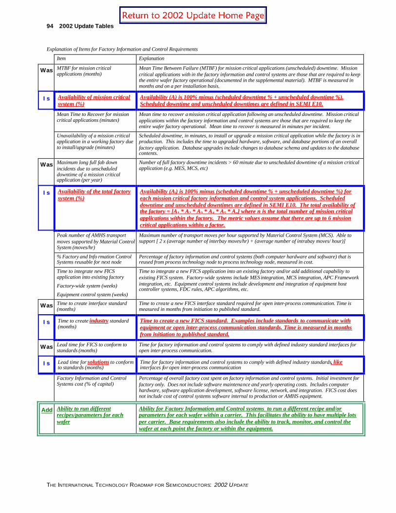
94 2002 Update Tables
THE INTERNATIONAL TECHNOLOGY ROADMAP FOR SEMICONDUCTORS: 2002 UPDATE
Explanation of Items for Factory Information and Control Requirements
Item Explanation
Was MTBF for mission critical applications (months)
Mean Time Between Failure (MTBF) for mission critical applications (unscheduled) downtime. Mission critical applications with in the factory information and control systems are those that are required to keep the entire wafer factory operational (documented in the supplemental material). MTBF is measured in months and on a per installation basis.
Is Availability of mission critical system (%)
Availability (A) is 100% minus (scheduled downtime % + unscheduled downtime %). Scheduled downtime and unscheduled downtimes are defined in SEMI E10.
Mean Time to Recover for mission critical applications (minutes)
Mean time to recover a mission critical application following an unscheduled downtime. Mission critical applications within the factory information and control systems are those that are required to keep the entire wafer factory operational. Mean time to recover is measured in minutes per incident.
Unavailability of a mission critical application in a working factory due to install/upgrade (minutes)
Scheduled downtime, in minutes, to install or upgrade a mission critical application while the factory is in production. This includes the time to upgraded hardware, software, and database portions of an overall factory application. Database upgrades include changes to database schema and updates to the database contents.
Was Maximum long full fab down incidents due to unscheduled downtime of a mission critical application (per year)
Number of full factory downtime incidents > 60 minute due to unscheduled downtime of a mission critical application (e.g. MES, MCS, etc)
Is Availability of the total factory system (%)
Availability (A i) is 100% minus (scheduled downtime % + unscheduled downtime %) for each mission critical factory information and control system applications. Scheduled downtime and unscheduled downtimes are defined in SEMI E10. The total availability of the factory = [A 1 * A 2 * A 3 * A 4 * A 5 * A n] where n is the total number of mission critical applications within the factory. The metric values assume that there are up to 6 mission critical applications within a factor.
Peak number of AMHS transport moves supported by Material Control System (moves/hr)
Maximum number of transport moves per hour supported by Material Control System (MCS). Able to support [ 2 x (average number of interbay moves/hr) + (average number of intrabay moves/ hour)]
% Factory and Info rmation Control Systems reusable for next node
Percentage of factory information and control systems (both computer hardware and software) that is reused from process technology node to process technology node, measured in cost.
Time to integrate new FICS application into existing factory
Factory-wide system (weeks)
Equipment control system (weeks)
Time to integrate a new FICS application into an existing factory and/or add additional capability to existing FICS system. Factory-wide systems include MES integration, MCS integration, APC Framework integration, etc. Equipment control systems include development and integration of equipment host controller systems, FDC rules, APC algorithms, etc.
Was Time to create interface standard (months)
Time to create a new FICS interface standard required for open inter-process communication. Time is measured in months from initiation to published standard.
Is Time to create industry standard (months)
Time to create a new FICS standard. Examples include standards to communicate with equipment or open inter-process communication standards. Time is measured in months from initiation to published standard.
Was Lead time for FICS to conform to standards (months)
Time for factory information and control systems to comply with defined industry standard interfaces for open inter-process communication.
Is Lead time for solutions to conform to standards (months)
Time for factory information and control systems to comply with defined industry standards, like interfaces for open inter-process communication
Factory Information and Control Systems cost (% of capital)
Percentage of overall factory cost spent on factory information and control systems. Initial investment for factory only. Does not include software maintenance and yearly operating costs. Includes computer hardware, software application development, software license, network, and integration. FICS cost does not include cost of control systems software internal to production or AMHS equipment.
Add Ability to run different recipes/parameters for each wafer
Ability for Factory Information and Control systems to run a different recipe and/or parameters for each wafer within a carrier. This facilitates the ability to have multiple lots per carrier. Base requirements also include the ability to track, monitor, and control the wafer at each point the factory or within the equipment.

2002 Update Tables 95
THE INTERNATIONAL TECHNOLOGY ROADMAP FOR SEMICONDUCTORS: 2002 UPDATE
Table 70a Facilities Technology Requirements—Near-term Year of Production 2001 2002 2003 2004 2005 2006 2007
DRAM ½ Pitch (nm) 130 115 100 90 80 70 65
MPU / ASIC ½ Pitch (nm) 150 130 107 90 80 70 65
MPU Printed Gate Length (nm) 90 75 650 53 45 40 35
MPU Physical Gate Length (nm) 65 53 45 37 32 28 25
Wafer Diameter 300 mm 300 mm 300 mm 300 mm 300 mm 300 mm 300 mm
Cleanroom area as a % of total site building area 17% 17% 17% 17% 17% 17% 17%
Was Cleanroom area (m2) / wafer starts per month 1.5 1.5 1.5 1.5 1.5 1.5 1.5
Is
Manufacturing (Cleanroom) area/Wafer starts per month (m2/WSPM)
0.34 0.34 0.34 0.34 0.34 0.34 0.34
Was Classification of air cleanliness in the manufacturing (cleanroom) area
ISO Class 5 (Fed Class
100) or better
ISO Class 5 (Fed Class
100) or better
ISO Class 5 (Fed Class
100) or better
ISO Class 6 (Fed Class
1000 or worse)
ISO Class 6 (Fed Class
1000 or worse)
ISO Class 6 (Fed Class
1000 or worse)
ISO Class 6 (Fed Class
1000 or worse)
Is Classification of air cleanliness in the manufacturing (cleanroom) area
ISO Class 5
ISO Class 5
ISO Class 5
ISO Class 6
ISO Class 6
ISO Class 6
ISO Class 6
Power utilization (demand/installed)
Gas and chemical purity Performance requirements enabling facilities to prevent defects and maintain process critical fluids and materials purity requirements are discussed in the Yield Enhancement Chapter
Power and water consumption Performance requirements affecting facilities involving natural resources conservation are discussed in the ESH chapter and involving gases, chemicals, exhaust, emissions, and utilities usage are discussed in the Process Equipment section of this chapter.
Factory construction time from ground break to all facility systems operational (months)
12 12 12 10 10 10 10
Facility capital cost as a % of total factory capital cost (includes equipment)
15% 15% 15% 15% 15% 15% 15%
Was Production equipment install and qualification cost as a % of capital cost
10% 8% 8% 6% 6% 6% 6%
Is Production equipment install and qualification cost as a % of capital cost
10% 8% 8% 6% 6% 6% 6%
Facility operating cost including utilities as a % of total operating cost
13% 13% 13% 13% 13% 13% 13%
Utility cost per total factory operating cost (%) 3% 3% 3% 3% 3% 3% 3%
Maximum allowable electrostatic field on facility surfaces (V/cm)
150 150 100 100 75 75 50
White–Manufacturable Solutions Exist, and Are Being Optimized
Yellow–Manufacturable Solutions are Known
Red–Manufacturable Solutions are NOT Known

96 2002 Update Tables
THE INTERNATIONAL TECHNOLOGY ROADMAP FOR SEMICONDUCTORS: 2002 UPDATE
Table 70b Facilities Technology Requirements —Long-term
Year of Production 2010 2013 2016
DRAM ½ Pitch (nm) 45 32 22
MPU / ASIC ½ Pitch (nm) 45 32 22
MPU Printed Gate Length (nm) 25 18 13
MPU Physical Gate Length (nm) 18 13 9
Wafer Diameter 300 mm 450 mm 450 mm
Cleanroom area as a % of total site building area 17% 17% 17%
Was Cleanroom area (m2) / wafer starts per month 1.5 1.5 1.5
Is Manufacturing (Cleanroom) area/Wafer starts per month (m2/WSPM) 0.34 0.34 0.34
Was Classification of air cleanliness in the manufacturing (cleanroom) area
ISO Class 6 (Fed Class 1000 or
worse)
ISO Class 6 (Fed Class 1000 or
worse)
ISO Class 6 (Fed Class 1000 or
worse)
Is Classification of air cleanliness in the manufacturing (cleanroom) area ISO Class 7 ISO Class 8 ISO Class 9
Power utilization (demand/installed) 80% 70% 80%
Gas and chemical purity Performance requirements enabling facilities to prevent defects and maintain process critical fluids and materials purity requirements are discussed in the Yield Enhancement Chapter
Power and water consumption
Performance requirements affecting facilities involving natural resources conservation are discussed in the ESH chapter and involving gases, chemicals, exhaust, emissions, and utilities usage are discussed in the Process Equipment section of this chapter.
Factory construction time from ground break to all facility systems operational (months) 10 10 10
Facility capital cost as a % of total factory capital cost (includes equipment) 15% 15% 15%
Production equipment install and qualification cost as a % of capital cost 6% 8% 6%
Facility operating cost including utilities as a % of total operating cost
13% 13% 13%
Utility cost per total factory operating cost (%) 3% 3% 3%
Maximum allowable electrostatic field on facility surfaces (V/cm)
50 25 25
White–Manufacturable Solutions Exist, and Are Being Optimized
Yellow–Manufacturable Solutions are Known
Red–Manufacturable Solutions are NOT Known
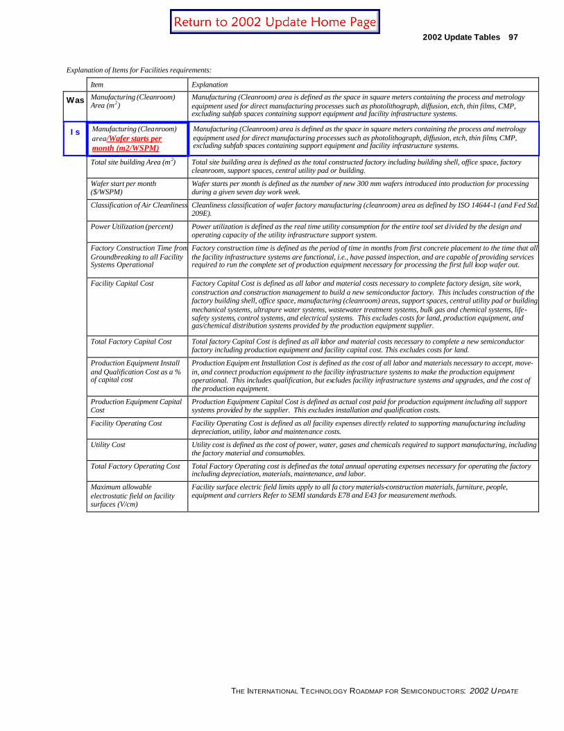
2002 Update Tables 97
THE INTERNATIONAL TECHNOLOGY ROADMAP FOR SEMICONDUCTORS: 2002 UPDATE
Explanation of Items for Facilities requirements:
Item Explanation
Was Manufacturing (Cleanroom) Area (m2)
Manufacturing (Cleanroom) area is defined as the space in square meters containing the process and metrology equipment used for direct manufacturing processes such as photolithograph, diffusion, etch, thin films, CMP, excluding subfab spaces containing support equipment and facility infrastructure systems.
Is Manufacturing (Cleanroom) area/Wafer starts per month (m2/WSPM)
Manufacturing (Cleanroom) area is defined as the space in square meters containing the process and metrology equipment used for direct manufacturing processes such as photolithograph, diffusion, etch, thin films, CMP, excluding subfab spaces containing support equipment and facility infrastructure systems.
Total site building Area (m2) Total site building area is defined as the total constructed factory including building shell, office space, factory cleanroom, support spaces, central utility pad or building.
Wafer start per month ($/WSPM)
Wafer starts per month is defined as the number of new 300 mm wafers introduced into production for processing during a given seven day work week.
Classification of Air Cleanliness Cleanliness classification of wafer factory manufacturing (cleanroom) area as defined by ISO 14644-1 (and Fed Std. 209E).
Power Utilization (percent) Power utilization is defined as the real time utility consumption for the entire tool set divided by the design and operating capacity of the utility infrastructure support system.
Factory Construction Time from Groundbreaking to all Facility Systems Operational
Factory construction time is defined as the period of time in months from first concrete placement to the time that all the facility infrastructure systems are functional, i.e., have passed inspection, and are capable of providing services required to run the complete set of production equipment necessary for processing the first full loop wafer out.
Facility Capital Cost Factory Capital Cost is defined as all labor and material costs necessary to complete factory design, site work, construction and construction management to build a new semiconductor factory. This includes construction of the factory building shell, office space, manufacturing (cleanroom) areas, support spaces, central utility pad or building, mechanical systems, ultrapure water systems, wastewater treatment systems, bulk gas and chemical systems, life-safety systems, control systems, and electrical systems. This excludes costs for land, production equipment, and gas/chemical distribution systems provided by the production equipment supplier.
Total Factory Capital Cost Total factory Capital Cost is defined as all labor and material costs necessary to complete a new semiconductor factory including production equipment and facility capital cost. This excludes costs for land.
Production Equipment Install and Qualification Cost as a % of capital cost
Production Equipm ent Installation Cost is defined as the cost of all labor and materials necessary to accept, move-in, and connect production equipment to the facility infrastructure systems to make the production equipment operational. This includes qualification, but excludes facility infrastructure systems and upgrades, and the cost of the production equipment.
Production Equipment Capital Cost
Production Equipment Capital Cost is defined as actual cost paid for production equipment including all support systems provided by the supplier. This excludes installation and qualification costs.
Facility Operating Cost Facility Operating Cost is defined as all facility expenses directly related to supporting manufacturing including depreciation, utility, labor and maintenance costs.
Utility Cost Utility cost is defined as the cost of power, water, gases and chemicals required to support manufacturing, including the factory material and consumables.
Total Factory Operating Cost Total Factory Operating cost is defined as the total annual operating expenses necessary for operating the factory including depreciation, materials, maintenance, and labor.
Maximum allowable electrostatic field on facility surfaces (V/cm)
Facility surface electric field limits apply to all fa ctory materials-construction materials, furniture, people, equipment and carriers Refer to SEMI standards E78 and E43 for measurement methods.

98 2002 Update Tables
THE INTERNATIONAL TECHNOLOGY ROADMAP FOR SEMICONDUCTORS: 2002 UPDATE
Table 71a Probe/Test Manufacturing Technology Requirements —Near-term
Year of Production 2001 2002 2003 2004 2005 2006 2007
DRAM ½ Pitch (nm) 130 115 100 90 80 70 65
MPU / ASIC ½ Pitch (nm) 150 130 107 90 80 70 65
MPU Printed Gate Length (nm) 90 75 650 53 45 40 35
MPU Physical Gate Length (nm) 65 53 45 37 32 28 25
Wafer Diameter 300 mm 300 mm 300 mm 300 mm 300 mm 300 mm 300 mm
Test product setup time improvement from previous year (complex devices) 0% 0% 0% 20% 10% 5% 5%
Test product setup time improvement from previous year (simple devices) 0% 0% 0% 5% 5% 5% 5%
1st article test equipment integration time improvement from previous year 0% 0% 30% 20% 20% 10% 10%
Mass produced test equipment integration time improvement from previous year 0% 0% 10% 10% 10% 5% 5%
White–Manufacturable Solutions Exist, and Are Being Optimized
Yellow–Manufacturable Solutions are Known
Red–Manufacturable Solutions are NOT Known
Table 71b Probe/Test Manufacturing Technology Requirements—Long-term
Year of Production 2010 2013 2016
DRAM ½ Pitch (nm) 45 32 22
MPU / ASIC ½ Pitch (nm) 45 32 22
MPU Printed Gate Length (nm) 25 18 13
MPU Physical Gate Length (nm) 18 13 9
Wafer Diameter 300 mm 450 mm 450 mm
Test product setup time improvement from previous year (complex devices) 5% 5% 5%
Test product setup time improvement from previous year (simple devices) 5% 5% 5%
1st article test equipment integration time improvement from previous year 10% 10% 10%
Mass produced test equipment integration time improvement from previous year 5% 5% 5%
White–Manufacturable Solutions Exist, and Are Being Optimized
Yellow–Manufacturable Solutions are Known
Red–Manufacturable Solutions are NOT Known

2002 Update Tables 99
THE INTERNATIONAL TECHNOLOGY ROADMAP FOR SEMICONDUCTORS: 2002 UPDATE
Explanation of Items for Probe/Test Manufacturing Technology Requirements:
Item Explanation
Delete Complex Devices Devices with >5M gates (e.g. high-performance, general purpose CPUs). Generally resulting in larger test programs (gigabytes), tester data output (10's of megabytes) and low product mix test cells.
Delete Simple Devices Devices with <5M gates (e.g. micro controllers, xRAMs). Generally resulting in smaller test programs (megabytes), tester data output (kilobytes) and high product mix test cells.
Delete Product Setup Time The time to perform the automated setup of a test cell (lot introduction, process program download, initialization) prior to material processing
Add Test product setup time improvement from previous year (complex devices)
Percent improvement in the time required to set up test equipment to test a complex semiconductor devices. Complex devices are defined as having >5M gates (e.g. high-performance, general purpose CPUs). Generally resulting in larger test programs (gigabytes), tester data output (10's of megabytes) and low product mix test cells.
Add Test product setup time improvement from previous year (simple devices)
Percent improvement in the time required to set up test equipment to test a simple semiconductor devices. Simple devices are defined as having<5M gates (e.g. micro controllers, xRAMs). Generally resulting in smaller test programs (megabytes), tester data output (kilobytes) and high product mix test cells.
Was 1st Article Equipment Integration Time The elapsed time required to submit requirements, analyze, design, implement and test the automated functionality of the first instance of equipment delivered to a given IC manufacturer.
Is 1st Article Equipment Integration Time improvement from previous year
Percent improvement from year to year in the elapsed time required to submit requirements, analyze, design, implement and test the automated functionality of the first instance of equipment delivered to a given IC manufacturer.
Was Mass Produced Equipment Integration Time
The elapsed time required to qualify for production the automated functionality of subsequent instances of equipment (from a given IC manufacturer's perspective).
Is Mass Produced Equipment Integration Time improvement from previous year
Percent improvement from year to year in the elapsed time required to qualify for production the automated functionality of subsequent instances of equipment (from a given IC manufacturer's perspective).
Delete SEM Specific Equipment Model. A SEM is a type of industry standard that describes the way a particular type of equipment behaves and communicates with the factory information and control system. The minimal equipment control behavior, messaging syntax/sequencing, data content, data collection and data modification mechanisms are specified in this type of standard.

100 2002 Update Tables
THE INTERNATIONAL TECHNOLOGY ROADMAP FOR SEMICONDUCTORS: 2002 UPDATE
ASSEMBLY AND PACKAGING Table 74 Assembly and Packaging Difficult Challenges [Update]
Difficult Challenges ≥ 65 nm / Through 2007 Summary of Issues
Was Improved organic substrates – Tg compatible with Pb free solder processing – Increased wireability at low cost – Improved impedance control and lower dielectric loss to support higher frequency applications – Improved planarity and low warpage at higher process temperatures – Low-moisture absorption – Low-cost embedded passives
Is Improved organic substrates – Tg compatible with Pb free solder processing – Increased wireability at low cost – Improved impedance control and lower dielectric loss to support higher frequency applications – Improved planarity and low warpage at higher process temperatures – Low-moisture absorption – Low-cost embedded passives –Substrate cost is barrier to flip chip adoption today
Was Improved underfills for flip chip on organic substrates
– Improve flow, fast dispense/cure, better interface adhesion, lower moisture absorption – Higher operating range for automotive in liquid dispense underfills – Improved adhesion, small filler size, and improved flow for mold based underfills
Is Improved underfills for flip chip on organic substrates
– Improve flow, fast dispense/cure, better interface adhesion, lower moisture absorption – Higher operating range for automotive and Pb free soldering in liquid dispense underfills – Improved adhesion, small filler size, and improved flow for mold based underfills –Issues are manufacturability for chip-size packages, compatibility with Harsh environments (automotive) and improved reliability for soldering processes
Was Coordinated design tools and simulators to address chip, package, and substrate co-design
– Mix signal co-design and simulation environment – Faster analysis tools for transient thermal analysis and integrated thermal mechanical analysis – Electrical (power disturbs, EMI†, signal integrity associated with higher frequency/current and lower voltage switching) – Commercial EDA‡ supplier support
Is Coordinated design tools and simulators to address chip, package, and substrate co-design
– Mix signal co-design and simulation environment – Faster analysis tools for transient thermal analysis and integrated thermal mechanical analysis – Electrical (power disturbs, EMI†, signal integrity associated with higher frequency/current and lower voltage switching) – Commercial EDA‡ supplier support –System level co-design is needed now. EDA support for "native" area array is required to meet the Roadmap projections. - Educational programs required to train engineers in these technologies/requirements.
Was Impact of Cu/low ? on packaging – Direct wirebond and bump to Cu – Bump and underfill technology to assure low ? dielectric integrity – Improved Mechanical strength of dielectrics – Interfacial adhesion
Is Impact of Cu/low ? on packaging – Direct wirebond and bump to Cu – Bump and underfill technology to assure low ? dielectric integrity – Improved Mechanical strength of dielectrics – Interfacial adhesion –Mechanisms to measure the critical properties need to be developed.
Pb, Sb, and Br free packaging materials – Lower cost materials and processes to meet new requirements, including higher reflow temperatures. – Reliability under thermal cycling (stress and moisture)

2002 Update Tables 101
THE INTERNATIONAL TECHNOLOGY ROADMAP FOR SEMICONDUCTORS: 2002 UPDATE
Table 74 Assembly and Packaging Difficult Challenges [Update](continued) Difficult Challenges < 65 nm / Beyond 2007 Summary of Issues
Package cost that may greatly exceed die cost – Research investments required for packaging cost reduction are decreasing
Small, high pad count – Array I/O pitches below 80 microns
Was High Frequency die – Substrate wiring density to support >20 lines/mm – Lower loss dielectrics – Skin effect above 10GHz
Is High Frequency die – Substrate wiring density to support >20 lines/mm – Lower loss dielectrics – Skin effect above 10GHz –"Hot spot" thermal management needs to be addressed before 2007. There is a "brick wall at 5 micron lines and spaces. Design TWG would like to have an upper bound on thermal management capability of future packages.
Was Close gaps between substrate technology and the chip – Interconnect density scaled to silicon (silicon I/O density increasing faster than the printed circuit
Is Close gaps between substrate technology and the chip – Interconnect density scaled to silicon (silicon I/O density increasing faster than the printed circuit –Production techniques will require silicon-like production and process technologies after 2005.
Was System level design capability to integrated chips, passives and substrates
– Partitioning of system designs and manufacturing across numerous companies will make required optimization for performance, reliability, and cost of complex systems very difficult. Complex standards for information types and management of information quality along with a structure for moving this information will be required.
Is System level design capability to integrate chips, passives and substrates
– Partitioning of system designs and manufacturing across numerous companies will make required optimization for performance, reliability, and cost of complex systems very difficult. Complex standards for information types and management of information quality along with a structure for moving this information will be required. –The thermal/mechanical issues must be included with the electrical issues described in the 2001 Roadmap. This is also an issue before 2007.Embedded passives may be integrated into the "bumps" as well as the substrates.
Add Electromigration is not addressed and will become a more limiting factor through this period. It must be addressed together with a thermal/mechanical reliability modeling.
–Electromigration may become a limiting factor as the current per unit area increases
SIP as addressed but the Roadmap does not deal with the critical issues of "systems" packaging. System designers and design tools need to contemplate these alternatives. Bumpless area array technologies will be needed during this period. Face-to-face packages is one example. Higher frequency, lower power and lower profile are driving forces. * CTE - Coefficient of thermal expansion
** UBM - Under bump metallurgy
†-EMI-Electromagnetic interference
‡ EDA-Electronic design automation

102 2002 Update Tables
THE INTERNATIONAL TECHNOLOGY ROADMAP FOR SEMICONDUCTORS: 2002 UPDATE
Table 75a Single -chip Packaging Technology Requirements—Near-term Year of Production 2001 2002 2003 2004 2005 2006 2007
DRAM ½ Pitch (nm) 130 115 100 90 80 70 65
MPU / ASIC ½ Pitch (nm) 150 130 107 90 80 70 65
MPU Printed Gate Length (nm) 90 75 65 53 45 40 35
MPU Physical Gate Length (nm) 65 53 45 37 32 28 25
Cost (Cents/Pin) [1][2]
Was Low Cost 0.30–0.75 0.28–0.68 0.26–0.62 0.25–0.56 0.24–0.51 0.23–0.46 0.22–0.41
Is
Low Cost, Hand held and Memory The color applies to the low end only and are due only to cost. The high end numbers are OK
0.30–0.75 0.30–0.62 0.30–0.56 Scale @ 5% per year
Was Hand-held 0.45–0.90 0.42–0.81 0.40–0.73 0.38–0.65 0.36–0.60 0.34–0.56 0.32–0.52
Is Hand-held Delete these categories
0.45–0.90 0.30–0.62 0.30–0.56 Scale @ 5% per year
Was Cost-performance 0.80–1.60 0.75–1.44 0.70–1.30 0.66–1.17 0.61–1.06 0.56–1.03 0.53–1.00
Is Cost-performance 0.80–1.60 0.75–1.30 Scale @ 5% per year high end keep low end due to added complexity (power, pad pitch, increased bumps per die,
etc)
High-performance 2.2 2.09 1.98 1.88 1.78 1.69 1.61
Was Harsh 0.45–4.00 0.40–3.60 0.36–3.20 0.32–2.88 0.29–2.59 0.26–2.33 0.23–2.11
Is Harsh Pb free will cause consolidation with other categories
0.45–4.00 0.40–3.60 0.36–3.20 0.32–2.88 0.29–2.59 0.26–2.33 0.23–2.11
Was Memory 0.36–1.54 0.34–1.39 0.32–1.26 0.30–1.14 0.28–1.03 0.27–0.93 0.27–0.84
Is Memory Delete these categories
0.36–1.54 0.34–1.39 0.32–1.26 0.30–1.14 0.28–1.03 0.27–0.93 0.27–0.84
Chip Size (mm2) [3]
Low Cost 57 59 61 63 65 65 65
Hand-held 57 59 61 63 65 65 65
Cost-performance 170 178 186 195 204 204 204
High-performance 310 310 310 310 310 310 310
Harsh 60 80 100 100 100 100 100
Memory 127 141 157 175 175 175 175
Power: Single Chip Package (Watts) [4]
Low Cost n/a n/a n/a n/a n/a n/a n/a
Hand-held 2.4 2.6 2.8 3.2 3.2 3.5 3.5
Was Cost-performance 61 75 81 85 92 98 104
Is Cost-performance 61 75 81 85 92 98 104
Was High-performance 130 140 150 160 170 180 190
Is High-performance 130 140 150 160 170 180 190
Harsh 14 14 14 16 16 18 18
Memory 1.2 1.4 1.6 1.8 2 2 2

2002 Update Tables 103
THE INTERNATIONAL TECHNOLOGY ROADMAP FOR SEMICONDUCTORS: 2002 UPDATE
Table 75a Single -chip Packaging Technology Requirements—Near-term (continued) Year of Production 2001 2002 2003 2004 2005 2006 2007
DRAM ½ Pitch (nm) 130 115 100 90 80 70 65
MPU / ASIC ½ Pitch (nm) 150 130 107 90 80 70 65
MPU Printed Gate Length (nm) 90 75 65 53 45 40 35
MPU Physical Gate Length (nm) 65 53 45 37 32 28 25
Core Voltage (Volts)
Was Low Cost 1.8 1.2 1.2 1.2 1.2 0.9 0.9
Is Low Cost 1.8 1.2 1.2 1.2 1 0.9 0.9
Was Hand-held 1.2 1.2 1.1–1.2 1.1–1.2 1.1–1.2 1.0–1.2 0.9–1.1
Is Hand-held 1.2 1.2 1.1–1.2 1.1–1.2 1 1.0–1.2 0.9–1.1
Was Cost-performance 1.8 1.5 1.5 1.2 1.2 0.9 0.9
Is Cost-performance 1.8 1.5 1.2 1.2 1 0.9 0.9
High-performance 1.1 1 1 1 0.9 0.9 0.7
Harsh 3.3 2.5 2.5 2.5 1.2 1.2 1.2
Was Memory 1.8 1.5 1.5 1.2 1.2 1.2 0.9
Is Memory 1.8 1.5 1.2 1.2 1 1.2 0.9
Package Pincount maximum [5][6]
Low Cost 90–338 100–371 112–408 122–448 134–494 144–534 160–598
Hand-held 100–420 112–464 122–508 134–560 144–616 160–680 176–748
Cost-performance 480–1200480–1320500–1452500–1600550–1760550–1936600–2140
Was High-performance 1700 1870 2057 2263 2489 2738 3012
Is High-performance 1700 1870 2057 2263 2489 2738 3012
Harsh 280 308 338 372 408 448 494
Memory 44–128 44–144 44–144 48–160 48–160 48–160 48–160
Minimum Overall Package Profile (mm)
Low Cost 1 1 1 1 0.5 0.5 0.5
Hand-held 0.5 0.5 0.5 0.5 0.5 0.5 0.5
Was Cost-performance 1.0–1.2 1.0–1.2 1.0–1.2 0.8–1.2 0.8–1.2 0.8–1.2 0.8–1.2
Is Cost-performance 1.0–1.2 1 1 0.8 0.8 0.8 0.8
High-performance n/a n/a n/a n/a n/a n/a N/a
Harsh 1 1 1 1 1 1 1
Memory 1 1 1 0.8 0.5 0.5 0.5
White–Manufactu rable Solutions Exist, and Are Being Optimized
Yellow–Manufacturable Solutions are Known
Red–Manufacturable Solutions are NOT Known
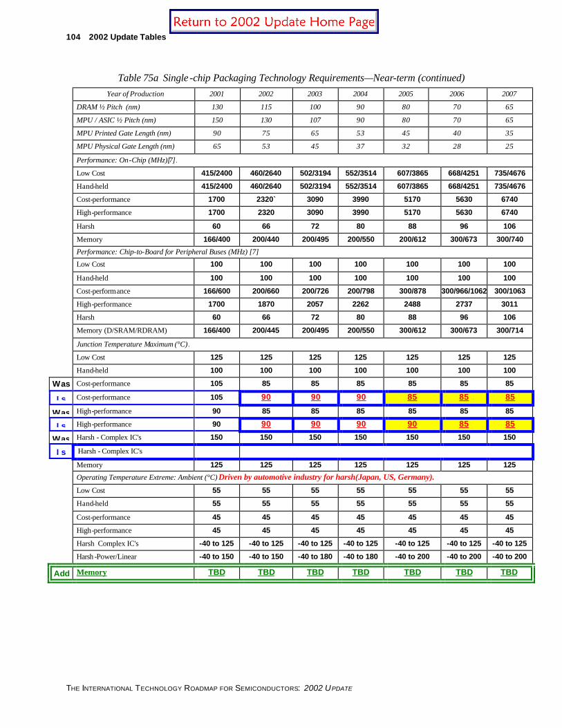
104 2002 Update Tables
THE INTERNATIONAL TECHNOLOGY ROADMAP FOR SEMICONDUCTORS: 2002 UPDATE
Table 75a Single -chip Packaging Technology Requirements—Near-term (continued) Year of Production 2001 2002 2003 2004 2005 2006 2007
DRAM ½ Pitch (nm) 130 115 100 90 80 70 65
MPU / ASIC ½ Pitch (nm) 150 130 107 90 80 70 65
MPU Printed Gate Length (nm) 90 75 65 53 45 40 35
MPU Physical Gate Length (nm) 65 53 45 37 32 28 25
Performance: On-Chip (MHz)[7].
Low Cost 415/2400 460/2640 502/3194 552/3514 607/3865 668/4251 735/4676
Hand-held 415/2400 460/2640 502/3194 552/3514 607/3865 668/4251 735/4676
Cost-performance 1700 2320` 3090 3990 5170 5630 6740
High-performance 1700 2320 3090 3990 5170 5630 6740
Harsh 60 66 72 80 88 96 106
Memory 166/400 200/440 200/495 200/550 200/612 300/673 300/740
Performance: Chip-to-Board for Peripheral Buses (MHz) [7]
Low Cost 100 100 100 100 100 100 100
Hand-held 100 100 100 100 100 100 100
Cost-performance 166/600 200/660 200/726 200/798 300/878 300/966/1062 300/1063
High-performance 1700 1870 2057 2262 2488 2737 3011
Harsh 60 66 72 80 88 96 106
Memory (D/SRAM/RDRAM) 166/400 200/445 200/495 200/550 300/612 300/673 300/714
Junction Temperature Maximum (°C).
Low Cost 125 125 125 125 125 125 125
Hand-held 100 100 100 100 100 100 100
Was Cost-performance 105 85 85 85 85 85 85
Is Cost-performance 105 90 90 90 85 85 85
Was High-performance 90 85 85 85 85 85 85
Is High-performance 90 90 90 90 90 85 85
Was Harsh - Complex IC's 150 150 150 150 150 150 150
Is Harsh - Complex IC's
Memory 125 125 125 125 125 125 125
Operating Temperature Extreme: Ambient (°C) Driven by automotive industry for harsh(Japan, US, Germany).
Low Cost 55 55 55 55 55 55 55
Hand-held 55 55 55 55 55 55 55
Cost-performance 45 45 45 45 45 45 45
High-performance 45 45 45 45 45 45 45
Harsh Complex IC's -40 to 125 -40 to 125 -40 to 125 -40 to 125 -40 to 125 -40 to 125 -40 to 125
Harsh -Power/Linear -40 to 150 -40 to 150 -40 to 180 -40 to 180 -40 to 200 -40 to 200 -40 to 200
Add Memory TBD TBD TBD TBD TBD TBD TBD

2002 Update Tables 105
THE INTERNATIONAL TECHNOLOGY ROADMAP FOR SEMICONDUCTORS: 2002 UPDATE
Table 75b Single -chip Packaging Technology Requirements—Long-term Note—same comments in red in Table 75a apply
Year of Production 2010 2013 2016
DRAM ½ Pitch (nm) 45 32 22
MPU / ASIC ½ Pitch (nm) 50 35 25
MPU Printed Gate Length (nm) 25 18 13
MPU Physical Gate Length (nm) 18 13 9
Cost (Cents/Pin)[1] [2]
Was Low Cost 0.22–0.49 0.19–0.42 0.19–0.39
Is Low Cost 0.22–0.49 0.19–0.42 0.19–0.39
Was Hand-held 0.27–0.70 0.23–0.67 0.20–0.56
Is Hand-held 0.27–0.70 0.23–0.67 0.20–0.56
Was Cost-performance 0.49–0.98 0.42–0.93 0.36–0.79
Is Cost-performance 0.49–0.98 0.42–0.93 0.36–0.79
High-performance 1.68 1.44 1.22
Harsh 0.27–1.54 0.23–1.12 0.20–.9
Was Memory 0.22–0.54 0.19–0.39 0.19–0.33
Is Memory 0.22–0.54 0.19–0.39 0.19–0.33
Chip Size (mm2)[3]
Low Cost 81 90 90
Hand-held 81 90 90
Cost-performance 268 307 307
High-performance 310 310 310
Harsh 150 150 150
Memory 191 250 250
Power: Single Chip Package (Watts)[4]
Low Cost N/A N/A N/A
Hand-held 3 3 3
Was Cost-performance 119.6 137.6 158.2
Is Cost-performance 119.6 137.6 158.2
Was High-performance 218 250.7 288.3
Is High-performance 218 250.7 288.3
Harsh 20.7 23.8 27.4
Memory 2.3 2.65 3.05
White–Manufacturable Solutions Exist, and Are Being Optimized
Yellow–Manufacturable Solutions are Known
Red–Manufacturable Solutions are NOT Known

106 2002 Update Tables
THE INTERNATIONAL TECHNOLOGY ROADMAP FOR SEMICONDUCTORS: 2002 UPDATE
Table 75b Single -chip Packaging Technology Requirements—Long-term (continued) Note—same comments in red in Table 75a apply
Year of Production 2010 2013 2016
DRAM ½ Pitch (nm) 45 32 22
MPU / ASIC ½ Pitch (nm) 50 35 25
MPU Printed Gate Length (nm) 25 18 13
MPU Physical Gate Length (nm) 18 13 9
Core Voltage (Volts)
Low Cost 0.6 0.5–0.6 0.3
Hand-held 0.5 0.4 0.4
Cost-performance 0.6 0.6 0.5
High-performance 0.6 0.5 0.4
Harsh 1.2 0.9 0.9
Memory 0.6 0.6 0.3
Package Pincount [5] [6]
Low Cost 208–777 270–1011 351–1314
Hand-held 229–972 298–1264 387–1643
Was Cost-performance 780–2782 1014–3616 1318–4702
Is Cost-performance 780–2782 1014–3616 1318–4702
Was High-performance 4009 5335 7100
Is High-performance 4009 5335 7100
Harsh 642 835 1086
Memory 62–208 81–270 105–351
Overall Package Profile (mm)
Was Low Cost 0.8 0.5 0.5
Is Low Cost 0.5 0.5 0.5
Was Hand-held 0.65 0.5 0.5
Is Hand-held 0.5 0.5 0.5
Was Cost-performance 0.65-0.8 0.50–0.65 0.5–0.65
Is Cost-performance 0.5 0.5 0.5
High-performance n/a n/a n/a
Harsh 1 1 0.8
Was Memory 0.65 0.5 0.5
Is Memory 0.5 0.5 0.5
White–Manufacturable Solutions Exist, and Are Being Optimized
Yellow–Manufacturable Solutions are Known
Red–Manufacturable Solutions are NOT Known

2002 Update Tables 107
THE INTERNATIONAL TECHNOLOGY ROADMAP FOR SEMICONDUCTORS: 2002 UPDATE
Table 75b Single -chip Packaging Technology Requirements—Long-term (continued) Note—same comments in red in Table 75a apply
Year of Production 2010 2013 2016
DRAM ½ Pitch (nm) 45 32 22
MPU / ASIC ½ Pitch (nm) 50 35 25
MPU Printed Gate Length (nm) 25 18 13
MPU Physical Gate Length (nm) 18 13 9
Performance: On-Chip (MHz) [7]
Low Cost 956–6079 1243–7903 1616–10274
Hand-held 956–6079 1243–7903 1616–10274
Cost-performance 12000 19000 29000
High-performance 12000 19000 29000
Harsh 138 179 234
Memory 450/984 600/1280 750/1665
Performance: Chip-to-Board for Peripheral Buses (MHz)[7]
Low Cost 125 125 150
Hand-held 125 125 150
Cost-performance 300/1415 300/1883 300/2506
High-performance 4009 5339 7100
Harsh 125 125 150
Memory (S/SRAM) 250/761 250/963 250/1175
Junction Temperature Maximum (°C) for Cost- performance
Low Cost 125 125 125
Hand-held 100 100 100
Was Cost-performance 85 85 85
Is Cost-performance 85 85 85
Was High-performance 85 85 85
Is High-performance 85 85 85
Harsh 150 150 150
Harsh-Complex IC's 190 190 190
Memory 100 100 100
Operating Temperature Extreme: Ambient (°C)
Low Cost 55 55 55
Hand-held 55 55 55
Cost-performance 45 45 45
High-performance 45 45 45
Harsh -40 to 125 -40 to 125 -40 to 125
Harsh -Complex IC's -40 to 150 -40 to 150 -40 to 150
Memory 55 55 55
White–Manufacturable Solutions Exist, and Are Being Optimized Yellow–Manufacturable Solutions are Known
Red–Manufacturable Solutions are NOT Known

108 2002 Update Tables
THE INTERNATIONAL TECHNOLOGY ROADMAP FOR SEMICONDUCTORS: 2002 UPDATE
Table 76 Comparison between Bare Chip Mounting and WLP Technology
Item Bare Chip Mounting Wafer Level Packaging
Package Type — – Real chip size package (FBGA)
Device Body Size – Same as chip size – Same as chip size
Terminal Design of Device – All terminal pads shall be located in adaptable pitch on chip
– All terminal pads shall be located in adaptable pitch on chip
Quality Assurance of Device – Difficult (especially burn in test) – Easy
Interconnection of Board – Wire bonding (WB) – Flip chip bonding (FCB) – Solder ball terminal
Interconnecting Wire Length – FCB can achieve the shortest connection length
– May be slightly longer than FCB for re-wire die and ball
Mounting Area on Board – Slight larger than chip area (fan-out for WB) – (Under fill print area for FCB)
– Same area as chip size
Reliability after Board Mounting – Encapsulation and under-fill material required – Near equal to conventional packages
Mountability on Board – Facility for bare chip assembly required – Difficult to repair
– Multiple parts reflow available – Easy to be repaired by standard SMT assembly process

2002 Update Tables 109
THE INTERNATIONAL TECHNOLOGY ROADMAP FOR SEMICONDUCTORS: 2002 UPDATE
Table 77 Chip to Next Level Potential Solutions Year of Production 2001 2002 2003 2004 2005 2006 2007 2010 2013 2016
DRAM ½ Pitch (nm) 130 115 100 90 80 70 65 45 32 22
MPU / ASIC ½ Pitch (nm ) 150 130 107 90 80 70 65 50 35 25
MPU Printed Gate Length (nm) 90 75 65 53 45 40 35 25 18 13
MPU Physical Gate Length (nm) 65 53 45 37 32 28 25 18 13 9
Chip Interconnect Pitch (µm)
Was Wire bond—ball 45 35 30 25 20 20 20 20 20 20
Is Wire bond—ball 45 40 35 30 25 20 20 20 20 20
Was Wire bond—wedge 40 35 30 25 20 20 20 20 20 20
Is Wire bond—wedge 50 50 40 40 35 35 30 20 20 20
Was TAB*. 40 40 40 40 30 30 30 30 30 30
Is TAB* Japan TWG has the lead for Tab technologies
45 40 35 35 30 30 25 20 20 15
Was Flip chip (area array for cost-performance and high-performance) 160 160 150 150 130 130 120 90 80 70
Is Flip chip area array 200 180 150 150 100 100 80 70 70 50
Was Peripheral flip chip for hand-held, low-cost, and harsh 150 130 120 110 100 90 80 60 45 30
Is Peripheral flip chip 80 80 60 60 40 40 30 20 20 15

110 2002 Update Tables
THE INTERNATIONAL TECHNOLOGY ROADMAP FOR SEMICONDUCTORS: 2002 UPDATE
Table 78 Ball Grid Array Packages Potential Solutions Year of Production 2001 2002 2003 2004 2005 2006 2007 2010 2013 2016
DRAM ½ Pitch (nm) 130 115 100 90 80 70 65 45 32 22
MPU / ASIC ½ Pitch (nm) 150 130 107 90 80 70 65 50 35 25
MPU Printed Gate Length (nm) 90 75 65 53 45 40 35 25 18 13
MPU Physical Gate Length (nm) 65 53 45 37 32 28 25 18 13 9
BGA Solder Ball Pitch (mm)
Was Low cost 1 1 0.8 0.8 0.65 0.65 0.65 0.5 0.5 0.5
Is Low cost 1 0.8 0.8 0.8 0.5 0.5 0.5 0.5 0.5 0.5
Was Hand-Held 1 1 0.8 0.8 0.65 0.65 0.65 0.5 0.5 0.5
Is Hand-Held 1 0.8 0.8 0.8 0.5 0.5 0.5 0.5 0.5 0.5
Was Cost-performance 1 1 0.8 0.8 0.65 0.65 0.65 0.5 0.5 0.5
Is Cost-performance 1 1 1 0.8 0.8 0.8 0.5 0.5 0.5 0.5
Was High-Performance 0.8 0.8 0.8 0.8 0.65 0.65 0.65 0.5 0.5 0.5
Is High-Performance 0.8 1 1 1 1 0.8 0.8 0.8 0.8 0.8
Was Harsh 1.27 1.27 1 1 1 0.8 0.65 0.5 0.5 0.5
Is Harsh 1.27 1.27 1 1 1 0.8 0.8 0.5 0.5 0.5

2002 Update Tables 111
THE INTERNATIONAL TECHNOLOGY ROADMAP FOR SEMICONDUCTORS: 2002 UPDATE
Table 79 Single Chip Packages Potential Solutions
Year of Production 2001 2002 2003 2004 2005 2006 2007 2010 2013 2016
DRAM ½ Pitch (nm) 130 115 100 90 80 70 65 45 32 22
MPU / ASIC ½ Pitch (nm) 150 130 107 90 80 70 65 50 35 25
MPU Printed Gate Length (nm) 90 75 65 53 45 40 35 25 18 13
MPU Physical Gate Length (nm) 65 53 45 37 32 28 25 18 13 9
Was FBGA/CSP area array pitch (mm) 0.4 0.4 0.4 0.4 0.3 0.3 0.3 0.3 0.3 0.3
Is FBGA/CSP area array pitch (mm) 0.5 0.5 0.4 0.4 0.3 0.3 0.2 0.15 0.15 0.1
Was FBGA/CSP size (mm/side) 10 10 10 10 10 10 10 10 10 10
Is FBGA/CSP size (mm/side) 4–21 4–21 4–21 4–21 4–21 4–21 4–21 4–21 4–21 4–21
Table 80 BGA and FBGA/CSP Package Substrate Potential Solutions Year of Production 2001 2002 2003 2004 2005 2006 2007 2010 2013 2016
DRAM ½ Pitch (nm) 130 115 100 90 80 70 65 45 32 22
MPU / ASIC ½ Pitch (nm) 150 130 107 90 80 70 65 50 35 25
MPU Printed Gate Length (nm) 90 75 65 53 45 40 35 25 18 13
MPU Physical Gate Length (nm) 65 53 45 37 32 28 25 18 13 9
Was FBGA/CSP solder ball pad pitch (mm) 0.4 0.4 0.4 0.4 0.3 0.3 0.3 0.3 0.3 0.25
Is FBGA/CSP solder ball pad pitch (mm) 0.5 0.5 0.4 0.4 0.3 0.3 0.2 0.15 0.15 0.1
Was Pad size (µm) 160 160 160 160 120 120 120 120 120 100
Is Pad size (µm) 200 200 160 160 120 120 120 120 120 100
Was Line width (µm) 48 48 48 48 36 36 36 36 36 30
Is Line width (µm) 60 60 48 48 36 36 24 18 18 12
Was Line spacing (µm) 48 48 48 48 36 36 36 36 36 30
Is Line spacing (µm) 60 60 48 48 36 36 24 18 18 12
# Rows accessed 3 3 3 3 3 3 3 3 3 3

112 2002 Update Tables
THE INTERNATIONAL TECHNOLOGY ROADMAP FOR SEMICONDUCTORS: 2002 UPDATE
ENVIRONMENT , SAFETY, AND HEALTH Table 82 Environment, Safety, and Health Difficult Challenges
Five Difficult Challenges ≥ 65 nm, Through 2007
Summary of Issues/Needs
New Chemical Assessment
Need for quality rapid assessment methodologies to ensure that new chemicals can be utilized in manufacturing, while protecting human health, safety, and the environment without delaying process implementation. Chemicals in existing uses require reassessment when new chemical restrictions are identified.
Chemical Data Collection
Need to document and make available environment, safety, and health characteristics of chemicals.
Chemical Reduction
Need to develop processes that meet technology demands while reducing impact on hum an health, safety and the environment, both through replacement of hazardous materials with materials that are more benign, and by reducing chemical quantity requirements through more efficient and cost -effective process management.
Environment Management
Chemicals, Materials and Equipment Management
Need to develop effective management systems to address issues related to disposal of equipment, and hazardous and non-hazardous residue from the manufacturing process.
Natural Resource Conservation (Energy, Water)
Need to design more energy and water efficient processing equipment.
Chemicals and Materials Use
Need more efficient utilization of chemicals and materials.
Resource Recycling
Resource Conservation
Increase resource reuse and recycling.
Equipment Safety
Need to design ergonomically correct and safe equipment.
Chemical Exposure Protection
Workplace Protection
Increase knowledge base on health and safety characteristics of chemicals and materials used in the manufacturing and maintenance processes, and of the process byproducts; and implement safeguards to protect the users of the equipment and facility.
Reduce Energy Use of Process Equipment
Need to design energy efficient larger wafer size processing equipment.
Reduce Energy Use of the Manufacturing Facility
Need to design energy efficient facilities to offset the increasing energy requirements of higher class clean rooms.
Reduce High Global Warming Potential (GWP) Chemicals Emission
Climate Change Mitigation
Need ongoing improvement in methods that reduce emissions from processes using GWP chemicals.
Evaluate and Quantify ESH Impact ESH Design and Measurement Methods
Need integrated way to evaluate and quantify ESH impact of process, chemicals, and process equipment, and to make ESH a design parameter in develo pment procedures for new equipment and processes.

2002 Update Tables 113
THE INTERNATIONAL TECHNOLOGY ROADMAP FOR SEMICONDUCTORS: 2002 UPDATE
Table 83a ESH Intrinsic Requirements—Near-term
Year of Production 2001 2002 2003 2004 2005 2006 2007 DRIVER
Dram 1/2 Pitch (nm) 130 115 100 90 80 70 65
Chemicals, Materials, and Equipment Management Technology Requirements
Assessment of Chemical and By-product Properties
Data accumulation Existing chemicals (include by -product materials)
50% of the data/chemical
100% of the data/chemical
New restrictions
New chemicals (include by-product materials)
Design of Data Base
100% after 2
years of market introduction
New processes
Resource Conservation Technology Requirements
Energy Consumption
Overall fab equipment (KWh/cm2) 0.5-0.7 0.4-0.5 0.3-0.4
Fab facility (kWh/cm2) 0.5-0.7 0.4-0.5 0.3-0.4
Tool energy usage per wafer pass (300mm versus 200mm); baseline 1999 1.5 1
Sustainable Growth
Water Consumption
Net feed water use (Liters/cm2) 5.9 3.5 3.5
Fab UPW use (Liters/cm2) 6 - 8 5 - 7 4 - 6
Tool UPW Use (Liters/cm2, per wafer pass) 0.15 0.075 0.06
Cost and sustainable
growth
Chemical Consumption & Waste Reduction
Chemical Use (liters/cm2/mask layer) Reduced 5% per year Reduced 5% per year
Recycle/Reuse Systems Infrastructure improvement
Thorough recycle/reuse
system
Innovative recycling
technologies
Waste recycle rate (%) 60% 65% 70%
Environmental stewardship
Climate Change Mitigation Technology Requirements
Reduce PFC emission 10% absolute reduction from 1995 baseline by 2010 as agreed to by the WSC
Voluntary agreement
Workplace Protection Technology Requirement
Equipment safety, gases and chemical leaks, and equipment stability during an earthquake
Conformance to S2 Safety Guidelines and S8
Ergonomic/Human Factor Guidelines
Conformance to revisions of S2 Safety
Guidelines and S8 Ergonomic/Human Factor Guidelines
Safe Interface of Automated Material Handling Systems (AMHS) and manufacturing equipment
Standardized control features and procedures
Safe Robotics Standardized control features and procedures
Data collection Comprehensive industrial
hygiene(IH) exposure data for operations and maintenance
Comprehensive exposure data
Collaboration among government, industry, academia, and companies regarding new exposure
data
Personal protection equipment (PPE) Investigation of PPE Test and rate PPE
Material Safety Data Sheets (MSDS) Employee
awareness for new technologies
Comprehensive data
Equipment Risk Assessment (Health and Safety) Case Study Common Algorithm Common Application
Reduced chemical exposure Workers isolated from chemicals and by-product for non-routine operation and maintenance
Ergonomic Improvement Basic Study for 300mm
Minimized/eliminated physiological stresses

114 2002 Update Tables
THE INTERNATIONAL TECHNOLOGY ROADMAP FOR SEMICONDUCTORS: 2002 UPDATE
Table 83a ESH Intrinsic Requirements—Near-term (continued) Year of Production 2001 2002 2003 2004 2005 2006 2007 DRIVER
Dram 1/2 Pitch (nm) 130 115 100 90 80 70 65
Design for ESH (DFESH)
Was Environmental load/impact assessment (LCA) Case Study
Common Algorithm to identify, access, and accept risk
Common Algorithm to identify, access, and
accept risk
Is Environmental load/impact assessment (LCA) Common Algorithm to identify and assess risk
Was Chemical Risk Assessment (Health and Safety) Case Study Common Algorithm to identify,
access, and accept risk
Common Algorithm to identify, access, and
accept risk
Is Chemical Risk Assessment (Health and Safety) Common Algorithm to identify and assess risk
Pollutant release, and transfer disclosure (PRTR)
PRTR data acquisition system New materials and restrictions
Material Balance
Common Test Methods, Protocol, and Application
Regulatory Requirements Collection of requirements, guidelines, policy trends, and others
White–Manufactu rable Solutions Exist, and Are Being Optimized
Yellow–Manufacturable Solutions are Known
Red–Manufacturable Solutions are NOT Known

2002 Update Tables 115
THE INTERNATIONAL TECHNOLOGY ROADMAP FOR SEMICONDUCTORS: 2002 UPDATE
Table 84a Chemicals, Materials and Equipment Management Technology Requirements—Near-term Year of Production 2001 2002 2003 2004 2005 2006 2007 Driver
DRAM ½ Pitch (nm) 130 115 100 90 80 70 65
Interconnect
Low κ materials – spin on and CVD Lowest ESH impact
solvents/ CVD precursors
Emissions modeled ESH benign processes Speed, signal
loss
Copper processes Lowest ESH impact plating chemistries Plating bath recycle ESH benign processes Speed,
reliability
Advanced metallization Lowest ESH impact processes/ emissions characterization ESH benign processes
Planarization Slurry minimization Slurry recycling Slurry-less planarization Planarity
Plasma processes Etch abatement Alternative etch chemistries Lowest ESH impact etch chemistries
Characterization of plasma by-products Lowest ESH impact etch chemistries
Front end Processes
Characterization of high κ precursor
materials
Lowest ESH impact high κ materials
ESH benign processes
Transistor performance
Characterization of low-hazard deposition methods
Low-hazard
deposition methods
ESH benign processes
Transistor performance and device
development
High κ materials
High κ materials without
potentially toxic/bioaccumulative
metals (Pb, Ni)
Lowest hazard metal compounds Device development
Doping Sub-atmospheric delivery system Lowest hazard dopant materials and processes
Fundamental research on
surface/interface science
Ongoing research and integration of
solutions
Optimized surface preparation processes
Alternative wafer rinse methods Incorporation into new rinse/clean tools
Characterization of alternative cleaning methods
Incorporation into new clean tools
ESH benign cleans
Surface Prep
Elimination of sulfuric acid
Front end etch Characterization of plasma by-products Plasma process simulation-optimized processes for by-
product destruction
White–Manufa cturable Solutions Exist, and Are Being Optimized
Yellow–Manufacturable Solutions are Known
Red–Manufacturable Solutions are NOT Known

116 2002 Update Tables
THE INTERNATIONAL TECHNOLOGY ROADMAP FOR SEMICONDUCTORS: 2002 UPDATE
Table 84a Chemicals, Materials and Equipment Management Technology Requirements—Near-term (continued)
Year of Production 2001 2002 2003 2004 2005 2006 2007 Driver
DRAM ½ Pitch (nm) 130 115 100 90 80 70 65
Lithography
New Equipment Reduced feature size
Optical
Characterization of
ESH Impacts
Minimal ESH Impact for hazardous chemicals and
material compatibility
e-Beam
Characterization of
ESH Impacts
Minimal ESH Impact for ionizing radiation, ergonomics, chemical
consumption, and disposal
EUV
Characterization of ESH Impacts
Minimal ESH Impact for non-ionizing radiation, ergonomics,
chemical consumption, and disposal
Add EUV (Propose) Non-PFOS PAG for EUV Resist
Radiation
Fundamental research on X-ray
exposure
Requirements for x-ray exposure PPE and/or equipment defined
New Materials
Characterization of ESH Impacts
Minimal ESH Impact for new chemicals, purification
requirements, wastes, and emissions
Was Identification of PFOS applications PFOS Alternatives
Is Identification of PFOS
applications PFOS Alternatives for
non-critical uses* PFOS Alternatives for critical
uses*
White–Manufacturable Solutions Exist, and Are Being Optimized
Yellow–Manufacturable Solutions are Known
Red–Manufacturable Solutions are NOT Known
Add notes to Table 84a *Critical uses of PFOS includes use in a photomicrolithography process to produce semiconductors or similar components of electronic or other miniaturized devices” as a: –Component of a photoresist (including PAGs and surfactants) –Component of an anti-reflective coating

2002 Update Tables 117
THE INTERNATIONAL TECHNOLOGY ROADMAP FOR SEMICONDUCTORS: 2002 UPDATE
YIELD ENHANCEMENT Table 88 Yield Enhancement Difficult Challenges
Difficult Challenge ≥ 65 nm, Through 2007 Summary of Issues
Develop and Validate Systematic Yield Models—Process induced defects, equipment generated particles, product/processing measurements, and design/layout sensitivit ies have to be correlated to yield.
Correlate process-induced defects (PID), particles per wafer pass (PMP), product inspections, and in situ measurements.
Develop parametric and process-to-design mismatch yield-loss models.
Address sampling and statistical issues with ultra-small populations.
Increase Yield Model accuracy.
High Aspect Ratio Inspection—High-speed cost -effective tools must be developed that rapidly detect defects associated with high-aspect-ratio contacts/vias/trenches, and particularly defects near/at the bottom of these features.
Poor transmission of energy into bottom of via and back out to detection system
Large number of contacts and vias per wafer
Defect/Fault Sourcing for Rapid Yield Learning—Automated, intelligent analysis and reduction algorithms that correlate facility, design, process, test and WIP data must be developed to enable rapid root cause analysis of yield limiting conditions.
Circuit complexity grows exponentially and the ability to rapidly isolate failures on non-arrayed chips is needed.
Automated data/image mining and reduction algorithms must be developed to source defects from multiple data sources (facility, design, process and test.)
Correlation of Impurity Level to Yield —Methodology for employment and correlation of fluid/gas types to yield of a standard test structure/product.
Establish an employment methodology for each material type.
Define a standard test for yield/parametric effect.
Difficult Challenge < 65 nm, Beyond 2007 Summary of Issues Develop Yield Models that Include New Materials and
Integration—Models must comprehend greater parametric sensitivities, complex integration issues, ultra-thin film integrity, impact of circuit design, greater transistor packing, etc.
Develop test structures for new technology nodes.
Address complex integration issues.
Model ultra-thin film integrity issues.
Improve scaling methods for front-end processes including increased transistor packing density.
Defect Detection—Detection and simultaneous differentiation of multip le killer defect types is necessary at high capture rates and throughput.
Existing techniques trade-off throughput for sensitivity, but at predicted defect levels, both throughput and sensitivity are necessary for statistical validity.
Ability to detect particles at critical size may not exist.
Non-visual Defect Sourcing and Design for Manufacture and Test—Failure analysis tools and techniques are needed to enable localization of defects where no visual defect is detected. Also, IC designs must be optimized for a given process capability and must be testable/diagnosable.
Many defects that cause electrical faults are not detectable inline.
Tools are needed that enable design to process matching for optimum yields.
Also, testability/diagnose-ability must be designed into the IC for rapid electrical failure sourcing.
Precursors for New Materials—Required purity levels for delivered dielectric pre-cursors are not known or well understood.
Establish methodology for establishing purity standards for new dielectric pre-cursors.
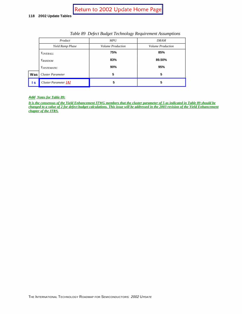
118 2002 Update Tables
THE INTERNATIONAL TECHNOLOGY ROADMAP FOR SEMICONDUCTORS: 2002 UPDATE
Table 89 Defect Budget Technology Requirement Assumptions Product MPU DRAM
Yield Ramp Phase Volume Production Volume Production
YOVERALL 75% 85%
YRANDOM 83% 89.50%
YSYSTEMATIC 90% 95%
Was Cluster Parameter 5 5
Is Cluster Parameter [A] 5 5
Add Notes for Table 89:
It is the consensus of the Yield Enhancement ITWG members that the cluster parameter of 5 as indicated in Table 89 should be changed to a value of 2 for defect budget calculations. This issue will be addressed in the 2003 revision of the Yield Enhancement chapter of the ITRS.

2002 Update Tables 119
THE INTERNATIONAL TECHNOLOGY ROADMAP FOR SEMICONDUCTORS: 2002 UPDATE
Table 90 Yield Model and Defect Budget MPU Technology Requirements Year of Production 2001 2002 2003 2004 2005 2006 2007 2010 2013 2016
DRAM ½ Pitch (nm) 130 115 100 90 80 70 65 45 32 22 MPU / ASIC ½ Pitch (nm) 150 130 107 90 80 70 65 50 35 25 MPU Printed Gate Length (nm) 90 75 65 53 45 40 35 25 18 13 MPU Physical Gate Length (nm) 65 53 45 37 32 28 25 18 13 9 MPU MPU ½ metal one Pitch (nm) [A] 150 130 107 90 80 70 65 45 32 22 Critical Defect Size (nm) 75 65 54 45 40 35 33 23 16 11 Chip Size (mm2) [B] 140 140 140 140 140 140 140 140 140 140
Overall Electrical D0 (faults/m2) at critical defect size or greater [C]
2115 2115 2115 2115 2115 2115 2115 2115 2115 2115
Random D0 (faults/m2) [D] 1356 1356 1356 1356 1356 1356 1356 1356 1356 1356 # Mask Levels [E] 25 25 25 25 25 27 27 27 29 29 Random Faults/Mask 54 54 54 54 54 50 50 50 47 47
MPU Random Particles per Wafer pass (PWP) Budget (defects/m2) for Generic Tool Type scaled to 75nm critical defect size or greater CMP Clean 448 337 228 161 127 90 78 37 18 8
CMP Insulator 1084 814 552 390 308 219 189 90 43 20 CMP Metal 1225 920 623 441 348 247 213 102 48 23
Coat/Develop/Bake 196 147 100 70 56 39 34 16 8 4 CVD Insulator 963 772 523 370 292 207 179 86 40 19
CVD Oxide Mask 1267 950 644 455 360 255 220 105 50 23 Dielectric Track 308 232 157 111 88 62 54 26 12 6
Furnace CVD 549 412 279 198 156 111 95 46 22 10 Furnace Fast Ramp 497 373 253 179 141 100 86 41 19 9
Furnace Oxide/Anneal 321 241 164 116 91 65 56 27 13 6 Implant High Current 430 323 219 155 122 87 75 36 17 8
Implant Low/Med Current 392 295 200 141 112 79 68 33 15 7 Inspect PLY 400 300 203 144 114 81 70 33 16 7
Inspect Visual 429 323 219 155 122 87 75 36 17 8 Litho Cell 332 250 169 120 95 67 58 28 13 6
Litho Stepper 315 237 160 113 90 64 55 26 12 6 Measure CD 374 281 190 135 106 75 65 31 15 7
Measure Film 321 241 164 116 91 65 56 27 13 6 Measure Overlay 298 224 152 107 85 60 52 25 12 6
Metal CVD 585 439 298 211 166 118 102 49 23 11 Metal Electroplate 302 227 154 109 86 61 52 25 12 6
Metal Etch 1300 976 661 468 370 262 226 108 51 24 Metal PVD 667 501 339 240 190 135 116 56 26 12
Plasma Etch 1183 889 602 426 336 239 206 99 46 22 Plasma Strip 547 411 278 197 156 110 95 46 21 10
RTP CVD 357 268 181 128 101 72 62 30 14 7 RTP Oxide/Anneal 234 175 119 84 66 47 41 19 9 4
Test 91 69 47 33 26 18 16 8 4 2 Vapor Phase Clean 822 617 418 296 234 166 143 68 32 15
Wafer Handling 37 28 19 13 10 7 6 3 1 1 Wet Bench 535 402 272 192 152 108 93 45 21 10
White–Manufacturable Solutions Exist, and Are Being Optimized Yellow–Manufacturable Solutions are Known
Red–Manufacturable Solutions are NOT Known

120 2002 Update Tables
THE INTERNATIONAL TECHNOLOGY ROADMAP FOR SEMICONDUCTORS: 2002 UPDATE
Notes for Table 90:
Was [A] As defined in the ORTC Table 1a
Is [A] As defined in the ORTC Table 1a+1b
Was [B] As defined in the ORTC Table 2a
Is [B] As defined in the ORTC Table 1g+1h
Was [C] As defined in the ORTC Table 5a)
Is [C] Based on assumption of 75% overall volume production yield.
Was [D] Based on assumption of 89.5% Random Defect Limited Yield (RDLY
Is [D] As defined in the ORTC Table 5a+5b. Based on assumption of 83% Random Defect Limited Yield (RDLY).
Was [E] As defined in the ORTC Table 5a
Is [E] As defined in the ORTC Table 5a+5b

2002 Update Tables 121
THE INTERNATIONAL TECHNOLOGY ROADMAP FOR SEMICONDUCTORS: 2002 UPDATE
Table 91 Yield Model and Defect Budget DRAM Technology Requirements Year of Production 2001 2002 2003 2004 2005 2006 2007 2010 2013 2016 DRAM ½ Pitch (nm) 130 115 100 90 80 70 65 45 32 22 MPU / ASIC ½ Pitch (nm) 150 130 107 90 80 70 65 50 35 25 MPU Printed Gate Length (nm) 90 75 65 53 45 40 35 25 18 13 MPU Physical Gate Length (nm) 65 53 45 37 32 28 25 18 13 9 DRAM DRAM ½ Pitch (nm) [A] 130 115 100 90 80 70 65 45 32 22 Critical Defect Size (nm) 65 58 50 45 40 35 33 23 16 11 Chip Size (mm2) [B] 127 100 118 93 147 116 183 181 240 238
Was Cell Array Area (%) @ Production 55% 55% 56% 56% 56% 57% 57% 58% 58% 58%
Is Cell Array Area (%) @ Production [B] 55% 55% 56% 56% 56% 57% 57% 58% 58% 58%
Non-Core Area (mm2) 57 45 52 41 64 50 79 77 101 99
Overall Electrical D0 (faults/m2) at critical defect size or greater [C]
2890 3671 3163 4047 2580 3293 2100 2155 1643 1670
Random D0 (faults/m2) [D] 1963 2493 2148 2748 1752 2236 1426 1464 1116 1134 # Mask Levels [E] 21 22 24 24 24 24 24 26 26 26 Random Faults/Mask 93 113 89 115 73 93 59 56 43 44 DRAM Random Particle per Wafer pass (PWP) Budget (defects/m2) for Generic Tool Type scaled to 75nm critical defect size or greater CMP Clean 1076 1021 610 632 318 311 171 78 30 14 CMP Insulator 833 790 472 489 246 241 132 60 23 11 CMP Metal 1276 1211 723 750 378 369 203 92 36 17 Coat/Develop/Bake 333 316 188 195 98 96 53 24 9 4 CVD Insulator 923 876 523 542 273 267 147 67 26 12 CVD Oxide Mask 1133 1075 642 665 335 327 180 82 32 15 Dielectric Track 467 443 264 274 138 135 74 34 13 6 Furnace CVD 638 605 361 374 189 184 101 46 18 9 Furnace Fast Ramp 601 571 341 353 178 174 96 43 17 8 Furnace Oxide/Anneal 481 456 272 282 142 139 76 35 13 6 Implant High Current 559 530 316 328 165 161 89 40 16 7 Implant Low/Med Current 533 506 302 313 158 154 85 38 15 7 Inspect PLY 729 691 413 428 216 211 116 53 20 10 Inspect Visual 752 713 426 441 222 217 119 54 21 10 Litho Cell 624 592 354 367 185 180 99 45 17 8 Litho Stepper 415 394 235 244 123 120 66 30 12 6 Measure CD 623 591 353 366 184 180 99 45 17 8 Measure Film 586 556 332 344 173 169 93 42 16 8 Measure Overlay 570 541 323 335 169 165 91 41 16 8 Metal CVD 587 557 333 345 174 170 93 42 16 8 Metal Electroplate 446 423 253 262 132 129 71 32 12 6 Metal Etch 1080 1025 612 634 320 312 172 78 30 14 Metal PVD 644 611 365 378 191 186 102 46 18 9 Plasma Etch 1144 1085 648 672 338 331 182 83 32 15 Plasma Strip 878 833 497 516 260 254 140 63 24 12 RTP CVD 574 545 325 337 170 166 91 41 16 8 RTP Oxide/Anneal 420 398 238 247 124 121 67 30 12 6 Test 82 78 46 48 24 24 13 6 2 1 Vapor Phase Clean 1215 1152 688 713 359 351 193 88 34 16 Wafer Handling 34 33 20 20 10 10 5 2 1 0 Wet Bench 870 825 493 511 257 251 138 63 24 12
White–Manufacturable Solutions Exist, and Are Being Optimized
Yellow–Manufacturable Solutions are Known
Red–Manufacturable Solutions are NOT Known

122 2002 Update Tables
THE INTERNATIONAL TECHNOLOGY ROADMAP FOR SEMICONDUCTORS: 2002 UPDATE
Notes for Table 91:
Was [A] As defined in the ORTC Table 1a
Is [A] As defined in the ORTC Table 1a+1b
Was [B] As defined in the ORTC Table 2a
Is [B] As defined in the ORTC Table 1c+1d
Was [C] As defined in the ORTC Table 5a)
Is [C] As defined in the ORTC Table 5a+5b. Based on assumption of 89.5% Random Defect Limited Yield (RDLY)
Was [D] Based on assumption of 89.5% Random Defect Limited Yield (RDLY
Is [D] As defined in the ORTC Table 5a+5b. Based on assumption of 89.5% Random Defect Limited Yield (RDLY). Variations from node to node in both overall electrical D 0 and random D 0 values for DRAM are driven predominantly by DRAM chip size variation. Chip size in turn is heavily influenced by a) the DRAM cell area factor and b) projected number of required functions per chip. The interaction of these two variables results in chip size increasing and decreasing with subsequent technology nodes (see ORTC Table 5a+5b). It is the consensus of the Yield Enhancement ITWG members that this variation of D 0 values and the subsequent variation of tool defect budget must addressed in the 2003 revision of the Yield Enhancement chapter of the ITRS to provide a consistent message of defect budget improvement out in time to process tool manufacturers.
Was [E] As defined in the ORTC Table 5a
Is [E] As defined in the ORTC Table 5a+5b

2002 Update Tables 123
THE INTERNATIONAL TECHNOLOGY ROADMAP FOR SEMICONDUCTORS: 2002 UPDATE
Table 93a Defect Detection Technology Requirements—Near-term Year of Production 2001 2002 2003 2004 2005 2006 2007 Driver DRAM ½ Pitch (nm) 130 115 100 90 80 70 65 MPU / ASIC ½ Pitch (nm) 150 130 107 90 80 70 65 MPU Printed Gate Length (nm) 90 75 65 53 45 40 35 MPU Physical Gate Length (nm) 65 53 45 37 32 28 25 Patterned Wafer Inspection, PSL* Spheres at 90% Capture, Equivalent Sensitivity (nm) [A, B]
Process R&D at 300 cm2/hr (1 wafer/hr) 78 72 66 54 48 42 39 0.6 x DR
Yield ramp at 1200 cm2/hr (4 wafer/hr) 104 96 88 72 65 56 52 0.8 x DR
Volume production at 3000 cm2/hr (10 wafer/hr) 130 120 110 90 80 70 66 1.0 x DR
High Aspect Ratio Feature Inspection: Defects other than Residue, Equivalent Sensitivity in PSL Diameter (nm) at 90% Capture Rate *[C]
All stages of manufacturing 130 120 110 90 80 70 65 1.0 x DR
Process verification (1 wafer/hr) 130 120 110 90 80 70 65 1.0 x DR
Volume manufacturing (4 wafer/hr) 130 120 110 90 80 70 65 1.0 x DR
Cost of Ownership :volume manufacturing, non-HARI ($/wafer scanned, 10/hr) 2–5 2–5 2–5 3–7 3–7 3–7 3–7
CoO HARI 20–50 20–50 20–50 20–50 20–50 20–50 20–50
Unpatterned, PSL Spheres at 90% Capture, Equivalent Sensitivity (nm) *[D, E, I]
Was Metal film 91 85 77 32 56 35 33 0.5 x DR
Is Metal film 65 60 55 45 40 35 33 0.5 x DR
Was Nonmetal films 70 65 59 49 43 35 33 0.5 x DR
Is Nonmetal films 65 60 55 45 40 35 33 0.5 x DR
Was Bare silicon 70 65 59 49 43 35 33 0.5 x DR
Is Bare silicon 65 60 55 45 40 35 33 0.5 x DR
Was Wafer backside 200mm (# events flip method) 2500 2000 2000 2000 2000 2000 1000
Is Wafer backside 200mm (# events flip method) 2500 2000 2000 2000 1000 1000 1000
Wafer backside 200mm (defect size nm) 200 200 200 200 100 100 100
Defect Review (Patterned wafer)
Resolution (nm) *[F] 7 7 6 5 5 4 3 0.05 x DR
Coordinate accuracy (µm) at resolution 2 2 1 1 1 1 1 (J)
Coordinate accuracy (µm) at size 15 12 12 10 10 7 7
Automatic Defect Classification at Defect Review Platform *[G, H]
Redetection: minimum defect size (nm) 52 48 44 36 30 28 26 0.4 x DR
Number of defect types 10 10 10 15 15 15 15 [K]
Speed (seconds/defect) 7 5 5 5 5 5 5
Speed w/elemental (seconds/defect) 20 15 13 10 10 10 10
White–Manufacturable Solutions Exist, and Are Being Optimized Yellow–Manufacturable Solutions are Known
Red–Manufacturable Solutions are NOT Known

124 2002 Update Tables
THE INTERNATIONAL TECHNOLOGY ROADMAP FOR SEMICONDUCTORS: 2002 UPDATE
Table 93b Defect Detection Technology Requirements—Long-term Year of Production 2010 2013 2016 DRIVER
DRAM ½ Pitch (nm) 45 32 22 MPU / ASIC ½ Pitch (nm) 50 35 25 MPU Printed Gate Length (nm) 25 18 13 MPU Physical Gate Length (nm) 18 13 9 Patterned Wafer Inspection, PSL Spheres at 90% Capture Process R&D at 300 cm2/hr (1 wafer/hr) 27 19 13 0.6 x DR
Yield ramp at 1200 cm2/hr (4wafer/hr) 36 26 18 0.8 x DR
Volume production at 3000 cm2/hr (10wafer/hr) 46 32 22 1.0 x DR
High Aspect Ratio Feature Inspection: Defects other than Residue All stages of manufacturing 45 32 22 1.0 x DR
Process verification (1 wafer/hr) 45 32 22 1.0 x DR
Volume manufacturing (4 wafer/hr) 45 32 22 1.0 x DR Cost of Ownership volume manufacturing, non-HARI ($/wafer scanned, 10 /hr) 3 - 7 3 - 5 3 - 5
CoO HARI 20 - 50 20 - 50 20 - 50
Unpatterned, PSL Spheres at 90% Capture, Equivalent Sensitivity (nm) [D, E]
Metal film 23 16 11 0.5 x DR Nonmetal films 23 16 11 0.5 x DR Bare silicon 23 16 11 0.5 x DR Wafer backside 200mm (# events flip method) 1000 1000 500
Wafer backside 200mm (defect size nm) 100 60 50 Defect Review (Patterned wafer) Resolution (nm) *[F] 3 2 2 0.05 x DR
Coordinate accuracy (µm) at resolution 0.5 0.5 0.5 [J]
Coordinate accuracy (µm) at size 5 5 5
Automatic Defect Classification at Defect Review Platform Re-detection minimum defect size (nm) 18 13 9 0.4 x DR Number of defect types 20 20 25 [K]
Speed (seconds/defect) 5 5 5 Speed w/elemental (seconds/defect) 10 10 10
White–Manufacturable Solutions Exist, and Are Being Optimized Yellow–Manufacturable Solutions are Known
Red–Manufacturable Solutions are NOT Known

2002 Update Tables 125
THE INTERNATIONAL TECHNOLOGY ROADMAP FOR SEMICONDUCTORS: 2002 UPDATE
Notes for Table 93a and b:
[A] Patterned wafer scan speed is required to be at least 300 cm2 /hour for process R&D mode, 1,200 cm2 /hour for yield ramp mode, and, at least, 3,000 cm2 /hour for volume production mode. Existing solutions do not achieve these targets at the above mentioned sensitivity requirement. The table indicates the approximate number of 200 mm wafers per hour. To obtain the approximate 300 mm wafers per hour, multiple the wafers/hour rate by .435. (Example-- 3000 cm2 /hr is about 10, 200 mm wafers and 4.3, 300 mm wafers).
[B] Patterned wafer nuisance defect rate shall be lower than 5% in all process phases. False counts in the R&D phase less than 5%, and less than 1% in the yield ramp and volume production phase. Nuisance is defined as an event indicated and a defect is present, just not the type of interest. These maybe significant and could be studied at a later date. The defect classifier must consider the defect type and assign significance. False is defined at an event is indicated, but no defect can be seen using the review optics path of the detection tool, which supports recipe setup validation.
[C] HARI defects are already considered “killers” at any process stage, but defined at the contact/via levels for full feature size capture. Hence, minimum defect sensitivity was stipulated as 1.0× technology node at all stages of production. Physically uninterrupted coverage of the bottom of a contact by a monolayer of material or more is the model to be detected. If in the future, detection tools can determine size, shape, or remaining material on the order of 0.3× technology node, this will more adequately match known experience for resistance changes. Scan speed for HARi tools have been broken out into process verification and volume production types. Process verification usually refers to SEM-type tools (but not necessarily in the future) and includes voltage contrast capability. The table indicates the approximate number of 200 mm wafers per hour. To obtain the approximate 300 mm wafers per hour, multiple the wafers/hour rate by .435.
Cost of Ownership is derived from the elements found in the International SEMATECH Metrology Tool Model.
Was [D] Unpatterned wafer defect detection tools will be required to scan 150 (200 mm or equivalent) wafers per hour at nuisance and false defect rates lower than 5%, for each individually.
Is [D] Un-patterned wafer defect detection tools will be required to scan 150 (200 mm or equivalent) wafers per hour at nuisance and false defect rates lower than 5%, for each individually. Must meet haze and crystal originated pit (COP) requirements specified in the starting material section of the roadmap.
[E] Metal films inspection tools must detect defects greater than half the minimum contacted pitch (Interconnect chapter technology requirements) × 0.6 (process R&D requirement for patterned wafer defects) for non-grainy films and × 0.6 for rough or grainy films. Nonmetal films and bare Si detection sensitivity must be at least as good as that for patterned wafer inspection to justify monitor wafer usage.
Backside wafer particles are specified as events found at the size indicated. The yellow indication is due to only some inspection tools being capability of meeting this added particle spec.
[F] Resolution corresponds to 10% of patterned wafer detection sensitivity for volume production.
[G] ADC: Detectability, as % of defects redetected, should be greater than 95; Accuracy, as the % of defects correctly classified as per a human expert, should be greater than 95; Repeatability should be greater than 95%; and Reproducibility, as COV%, should be no greater than 5%.
Was [H] Assumptions: 5,000 wafer starts per month, defects per wafer based on surface preparation at FEOL, leading to defects per hour that need review, 100% ADC.
Is [H] Assumptions: 5,000 wafer starts per week, defects per wafer based on surface preparation at FEOL, leading to defects per hour that need review, 100% ADC.
[I] Backside defects for 300 mm wafers is approximated by multiplying the 200 mm table values by 2.373. The defect sizes remain the same.
[J] Driver is redetection by SEM ADC instrument at a 5000× field of view.
[K] The trend of increasing numbers of defect types, read across the table, is also to indicate decreasing defect size.

126 2002 Update Tables
THE INTERNATIONAL TECHNOLOGY ROADMAP FOR SEMICONDUCTORS: 2002 UPDATE
Table 94a Yield Learning Technology Requirements—Near-term Year of Production 2001 2002 2003 2004 2005 2006 2007 DRAM ½ Pitch (nm) 130 115 100 90 80 70 65 MPU / ASIC ½ Pitch (nm) 150 130 107 90 80 70 65 MPU Printed Gate Length (nm) 90 75 65 53 45 40 35 MPU Physical Gate Length (nm) 65 53 45 37 32 28 25
Wafer size (mm) 300 300 300 300 300 300 300
Number of mask levels 25 25 25 27 27 27 29
Was Number of processing steps (simple logic) 490 503 516 530 543 556 570
Is Number of processing steps 490 503 516 530 543 556 570
Was Cycle time during ramp (# days) 25 25 25 27 27 27 29
Is Cycle time during ramp (# days) 38 38 38 41 41 41 44
Defect/Fault Sourcing Complexity [A], [G]
Logic transistor density/cm2 (1E6) 14 19 26 35 47 63 85
Defect sourcing complexity factor (1E9) [B] 7 10 13 18 25 35 49
Defect sourcing complexity trend [C] 1 1 2 3 4 5 7
Data Analysis for Rapid Defect/Fault Sourcing
Patterned wafer inspection sensitivity (nm) during yield ramp 104 96 88 72 64 56 52
Was Average # of inspections/wafer during full flow 5 5 5 5.4 5.4 5.4 5.8
Is Average # of inspections/wafer during full flow 2.5 2.5 2.5 2.7 2.7 2.7 2.9
Was Defect data volume (DV) (# data items/wafer) (1E13) [D] 5.5 7.1 9.4 12.5 15.8 20.7 25.7
Is Defect data volume (DV) (# data items/wafer) (1E13) [D] 2.75 3.55 4.7 6.25 7.9 10.35 12.85
Defect data volume (DV) trend [E] 1 1 2 2 3 4 5
Yield Learning During Ramp from 30% to 80% Sort Yield [F]
Was # of yield learning cycles/year based on full flow cycle time 14.6 14.6 14.6 13.5 13.5 13.5 12.6
Is # of yield learning cycles/year based on full flow cycle time 9.7 9.7 9.7 9.0 9.0 9.0 8.4
Was Required yield improvement rate per learning cycle 3.4 3.4 3.4 3.7 3.7 3.7 4
Is Required yield improvement rate per learning cycle 5.1 5.1 5.1 5.5 5.5 5.5 6.0
Was Time to identify and fix new defect/fault source during ramp 12.5 12.5 12.5 13.5 13.5 13.5 14.5
Is Time to identify and fix new defect/fault source during ramp 38 38 38 41 41 41 44
Was # of learning cycles/year for 1 defect/fault sources/month 8.6 8.6 8.6 7.5 7.5 7.5 6.6
Is # of learning cycles/year for 4 defect/fault source/year [I] 5.7 5.7 5.7 5.0 5.0 5.0 4.4
Was Required yield improvement rate/learning cycle for 1 defect/fault source/m onth
5.8 5.8 5.8 6.7 6.7 6.7 7.6
Is Required yield improvement rate/learning cycle for 4 defect/fault sources/year [I] 8.7 8.7 8.7 10.0 10.0 10.0 11.4
Excursion Control
Time to recognize defect trend TRT = f(T MP, N, TC, V) [H] * * * * * * *
Time to recognize electrical fault signature * * * * * * *
Time to identify defect mechanism TID = f(TRT, N, M, R) [H] * * * * * * *
Time to fix defect mechanism * * * * * * *
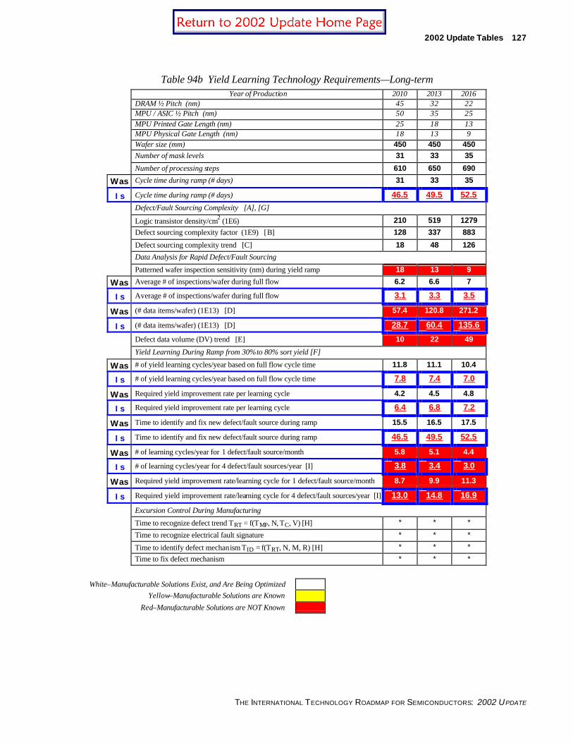
2002 Update Tables 127
THE INTERNATIONAL TECHNOLOGY ROADMAP FOR SEMICONDUCTORS: 2002 UPDATE
Table 94b Yield Learning Technology Requirements—Long-term Year of Production 2010 2013 2016 DRAM ½ Pitch (nm) 45 32 22 MPU / ASIC ½ Pitch (nm) 50 35 25 MPU Printed Gate Length (nm) 25 18 13 MPU Physical Gate Length (nm) 18 13 9 Wafer size (mm) 450 450 450
Number of mask levels 31 33 35
Number of processing steps 610 650 690
Was Cycle time during ramp (# days) 31 33 35
Is Cycle time during ramp (# days) 46.5 49.5 52.5
Defect/Fault Sourcing Complexity [A], [G]
Logic transistor density/cm2 (1E6) 210 519 1279
Defect sourcing complexity factor (1E9) [B] 128 337 883
Defect sourcing complexity trend [C] 18 48 126
Data Analysis for Rapid Defect/Fault Sourcing
Patterned wafer inspection sensitivity (nm) during yield ramp 18 13 9
Was Average # of inspections/wafer during full flow 6.2 6.6 7
Is Average # of inspections/wafer during full flow 3.1 3.3 3.5
Was (# data items/wafer) (1E13) [D] 57.4 120.8 271.2
Is (# data items/wafer) (1E13) [D] 28.7 60.4 135.6
Defect data volume (DV) trend [E] 10 22 49
Yield Learning During Ramp from 30% to 80% sort yield [F]
Was # of yield learning cycles/year based on full flow cycle time 11.8 11.1 10.4
Is # of yield learning cycles/year based on full flow cycle time 7.8 7.4 7.0
Was Required yield improvement rate per learning cycle 4.2 4.5 4.8
Is Required yield improvement rate per learning cycle 6.4 6.8 7.2
Was Time to identify and fix new defect/fault source during ramp 15.5 16.5 17.5
Is Time to identify and fix new defect/fault source during ramp 46.5 49.5 52.5
Was # of learning cycles/year for 1 defect/fault source/month 5.8 5.1 4.4
Is # of learning cycles/year for 4 defect/fault sources/year [I] 3.8 3.4 3.0
Was Required yield improvement rate/learning cycle for 1 defect/fault source/month 8.7 9.9 11.3
Is Required yield improvement rate/learning cycle for 4 defect/fault sources/year [I] 13.0 14.8 16.9
Excursion Control During Manufacturing
Time to recognize defect trend TRT = f(TMP, N, TC, V) [H] * * *
Time to recognize electrical fault signature * * *
Time to identify defect mechanism TID = f(TRT, N, M, R) [H] * * *
Time to fix defect mechanism * * *
White–Manufacturable Solutions Exist, and Are Being Optimized Yellow–Manufacturable Solutions are Known
Red–Manufacturable Solutions are NOT Known

128 2002 Update Tables
THE INTERNATIONAL TECHNOLOGY ROADMAP FOR SEMICONDUCTORS: 2002 UPDATE
Notes for Table 94a and b
[A] Defect/Fault sourcing means identifying the point of occurrence (identify process tool, design, test or process integration issue causing a visible or non-visual defect, parametric problem or electrical fault).
[B] Defect sourcing complexity factor = (logic transistor density #/ cm2)× (# processing steps)
[C] Defect sourcing complexity trend is normalized to 130nm technology node.
Was [D] Defect data volume (DV) = (# of inspection/wafer in process flow)(wafer area)/patterned wafer sensitivity during ramp Assumes 20% of wafers are inspected on average at each mask step during ramp.
Is [D] Defect data volume (DV) = (# of inspection/wafer in process flow)(wafer area)/patterned wafer sensitivity during ramp Assumes 10% of wafers are inspected on average at each mask step during ramp.
[E] DV trend is normalized to 130nm technology node.
Was [F] Assumes cycle time of one day per mask level. Also, assumes linear reduction in yield learning time based on time to identify and fix each defect/fault source.
Is [F] Assumes cycle time of 1.5 days per mask level. Also, assumes linear reduction in yield learning time based on time to identify and fix each defect/fault source.
[G] Rapid defect sourcing and yield learning assumptions as follows
• Keep yield ramp constant (30% intro yield to 80% mature yield) for successive technology nodes.
Was • Keep time to source new yield detractors to 50% of process cycle time.
Is • Keep time to source new yield detractors to 1X process cycle time.
• New material introduction should not increase defect/fault sourcing time.
• Focus defect/fault sourcing on ramp portion of yield learning curve.
• Data collection, retention and retrieval will go up exponentially and significant improvement will be required in th e IDM tools to enable the above assumptions.
[H] TMP, N, TC, V, M and R, respectively represent time between measurement points, number of process steps, cycle time, process variability, number of possible defect mechanisms and resources.
Add [I] Metric changed for 2002 from 1 defect/fault sources/month to 4 defect/fault sources/year.

2002 Update Tables 129
THE INTERNATIONAL TECHNOLOGY ROADMAP FOR SEMICONDUCTORS: 2002 UPDATE
Table 95a Wafer Environmental Contamination Control Technology Requirements—Near-term Year of Production 2001 2002 2003 2004 2005 2006 2007 DRAM ½ Pitch (nm) 130 115 100 90 80 70 65 MPU / ASIC ½ Pitch (nm) 150 130 107 90 80 70 65 MPU Printed Gate Length (nm) 90 75 65 53 45 40 35 MPU Physical Gate Length (nm) 65 53 45 37 32 28 25
Wafer Environment Control
Critical particle size (nm) [A] 65 58 52 45 38 35 33
# Particles > critical size (/m 3) [B] 5 4 3 2 2 1 1
Was Airborne Molecular Contaminants (ppt)) [C]
Is Airborne Molecular Contaminants (pptM)) [C] [I]
Lithography—bases (as amine, amide, or NH3) 750 750 750 750 750 <750 <750
Was Gate—metals (as Cu, E=2 × 10⁻⁵) [C] 0.2 0.2 0.15 0.1 0.1 0.07 <0.07
Is Gate—metals (as Cu, E=2 × 10⁻⁵) [C] 0.2 0.2 0.15 0.1 0.1 0.07 <0.07
Gate—organics (as molecular weight greater than or equal to 250, E=1 10-3) [D]
100 90 80 70 60 60 50 Was
Organics (as CH4) 1800 1620 1440 1260 1100 900 <900
Gate—organics (as molecular weight greater than or equal to 250, E=1 × 10⁻³) [D]
100 90 80 70 60 60 50 Is
Organics (as CH4) 1800 1620 1440 1260 1100 900 <900
Was Salicidation contact —acids (as Cl-, E=1 × 10⁻⁵) 10 10 10 10 10 <10 <10
Is Salicidation contact —acids (as Cl-, E=1 × 10⁻⁵) 10 10 10 10 10 <10 <10
Was Salicidation contact —bases (as NH3, E=1 ×10⁻⁶) 20 16 12 10 8 4 <4
Is Salicidation contact —bases (as NH3, E=1 ×10⁻⁶) 20 16 12 10 8 4 <4
Dopants (P or B) [E] <10 <10 <10 <10 <10 <10 <10
Process Critical Materials [I]
Critical particle size (nm) [A] 65 58 52 45 38 35 33
White–Manufacturable Solutions Exist, and Are Being Optimized
Yellow–Manufacturable Solutions are Known
Red–Manufacturable Solutions are NOT Known

130 2002 Update Tables
THE INTERNATIONAL TECHNOLOGY ROADMAP FOR SEMICONDUCTORS: 2002 UPDATE
Table 95a Wafer Environmental Contamination Control Technology Requirements—Near-term (continued) Year of Production 2001 2002 2003 2004 2005 2006 2007 DRAM ½ Pitch (nm) 130 115 100 90 80 70 65 MPU / ASIC ½ Pitch (nm) 150 130 107 90 80 70 65 MPU Printed Gate Length (nm) 90 75 65 53 45 40 35 MPU Physical Gate Length (nm) 65 53 45 37 32 28 25 Ultrapure Water Total oxidizable carbon (ppb) 1 1 <1 <1 <1 <1 <1 Bacteria (CFU/liter) <1 <1 <1 <1 <1 <1 <1 Total silica (ppb) 0.1 0.1 0.1 0.1 0.05 0.05 0.05
Add Reactive silica (ppb) 0.05 0.05 0.05 0.05 0.05 0.05 0.05
Was # Particles>critical size (/ml) <0.2 <0.2 <0.2 <0.2 <0.2 <0.2 <0.2
Is # Particles>critical size (/ml) [A] <0.2 <0.2 <0.2 <0.2 <0.2 <0.2 <0.2
Add Dissolved Oxygen (ppb) (contaminant based) 10 7 3 1 1 1 1
Add Dissolved Oxygen (%value) (process variable based) +/- 20 +/- 20 +/- 20 +/- 20 +/- 20 +/- 20 +/- 20
Was Critical cation, anion, metals (ppt, each) <20 <20 <20 10 10 10 10
Is Critical cation, anion, metals (ppt, each) [G] <10 <10 <10 <5 <5 <5 <1
Add Boron (ppt, each) 50 50 50 50 50 50 50
Add Temperature Stability (deg C) +/- 1 +/- 1 +/- 1 +/- 1 +/- 1 +/- 1 +/- 1
Liquid Chemicals [F] Was Particles—critical size (ml) <10 <10 <10 <10 <1 <1 <1
Is # Particles>critical size (/ml) [A] <10 <10 <10 <10 <1 <1 <1
HF-, H2O2, NH4OH: Fe, Cu (ppt, each) <150 <135 <110 <100 <90 <50 <50 Was Critical cation, anion, metals (ppt, each) <10 <10 <10 <5 <5 <5 <1
Is Critical cation, anion, metals (ppt, each) [G] <10 <10 <10 <5 <5 <5 <1
Was HF-only, TOC (ppb) <30 <30 <25 <20 <15 <10 <10
Is HF-only, TOC (ppb) [H] <30 <30 <25 <20 <15 <10 <10
HCl, H2SO4: All impurities (ppt) <1000 <1000 <1000 <1000 <1000 <1000 <1000 BEOL Solvents, Strippers K, Li, Na, (ppt, each) <1000 <1000 <1000 <1000 <1000 <1000 <1000 ILD CVD Precursors (e.g., TEOS) Metals (ppb) <1 <1 <1 <0.1 <0.1 <0.1 <0.1 H2O (ppmV) <10 <10 <10 <5 <5 <5 <1 Bulk Gases N2, O2, Ar, H2: H2O, O2, CO2, CH4 (ppt, each) <1000 <1000 <1000 <1000 <1000 <100 <100 # Particles > critical size (/liter) <0.1 <0.1 <0.1 <0.1 <0.1 <0.1 <0.1 Specialty Gases # POU particles > critical size (/liter) [F] 2 2 2 2 2 2 2 Inerts—Oxide/Photoresist Etchants/Strippers O2 (ppbV) <1000 <1000 <1000 <500 <500 <500 <100 H2O (ppbV) <1000 <1000 <1000 <500 <500 <500 <100 Individual specified metals (ppbWT) <10 <10 <10 <10 <10 <1 <1
White–Manufacturable Solutions Exist, and Are Being Optimized Yellow–Manufacturable Solutions are Known
Red–Manufacturable Solutions are NOT Known

2002 Update Tables 131
THE INTERNATIONAL TECHNOLOGY ROADMAP FOR SEMICONDUCTORS: 2002 UPDATE
Table 95b Wafer Environmental Contamination Control Technology Requirements—Long-term Year of Production 2010 2013 2016 DRAM ½ Pitch (nm) 45 32 22 MPU / ASIC ½ Pitch (nm) 50 35 25 MPU Printed Gate Length (nm) 25 18 13 MPU Physical Gate Length (nm) 18 13 9 Wafer Environment Control Critical particle size (nm) [A] 23 16 11 # Particles > critical size (/m 3) [B] 1 <1 <1
Was Airborne Molecular Contaminants (ppt) [C]
Is Airborne Molecular Contaminants (pptM)) [C]
Lithography—bases (as amine, amide, or NH3) <750 <750 <750 Was Gate—metals (as Cu, E=2 × 10⁻⁵) [C] <0.07 <0.07 <0.07
Is Gate—metals (as Cu, E=2 × 10⁻⁵) [C] <0.07 <0.07 <0.07
Was Gate—organics (as molecular weight greater than or equal to 250, E=1 10-3) [D] 40 30 20
Is Gate—organics (as molecular weight greater than or equal to 250, E=1 × 10⁻³) [D]
40 30 20
Organics (as CH4) <900 <900 <900 Was Salicidation contact —acids (as Cl-, E=1 × 10⁻⁵) <10 <10 <10
Is Salicidation contact —acids (as Cl-, E=1 × 10⁻⁵) <10 <10 <10
Was Salicidation contact —bases (as NH3, E=1 ×10⁻⁶) <4 <4 <4
Is Salicidation contact —bases (as NH3, E=1 ×10⁻⁶) <4 <4 <4
Dopants (P or B) [E] <10 <10 <10 Process Critical Materials Critical particle size (nm) [A] 23 16 11 Ultrapure Water Total oxidizable carbon (ppb) <1 <1 <1 Bacteria (CFU/liter) <1 <1 <1 Total silica (ppb) 0.01 <0.01 <0.01
Was Reactive silica (ppb) blank blank blank
Is Reactive silica (ppb) 0.01 0.01 0.01
Was Particles—critical size (ml) <0.2 <0.2 <0.2
Is # Particles>critical size (/ml) <0.2 <0.2 <0.2
Was Dissolved Oxygen (ppb) (contaminant based) blank blank blank
Is Dissolved Oxygen (ppb) (contaminant based) 1 1 1 Was Dissolved Oxygen (%value) (process variable based) blank blank blank
Is Dissolved Oxygen (%value) (process variable based) +/- 10 +/- 10 +/- 10
Was Critical cation, anion, metals (ppt, each) <10 <10 <10
Is Critical cation, anion, metals (ppt, each) [G] <1 <1 <1
Was Boron (ppt, each) blank blank blank
Is Boron (ppt, each) 50 50 50 Was Temperature Stability (deg C) blank blank blank
Is Temperature Stability (deg C) +/- 1 +/- 1 +/- 1
White–Manufacturable Solutions Exist, and Are Being Optimized
Yellow–Manufacturable Solutions are Known
Red–Manufacturable Solutions are NOT Known

132 2002 Update Tables
THE INTERNATIONAL TECHNOLOGY ROADMAP FOR SEMICONDUCTORS: 2002 UPDATE
Table 95b Technology Requirements for Wafer Environmental Contamination Control—Long-term (continued)
Year of Production 2010 2013 2016 DRAM ½ Pitch (nm) 45 32 22 MPU / ASIC ½ Pitch (nm) 50 35 25 MPU Printed Gate Length (nm) 25 18 13 MPU Physical Gate Length (nm) 18 13 9
Liquid Chemicals [F]
# Particles > critical size (/ml) <1 <1 <1
HF-, H2O2, NH4OH: Fe, Cu (ppt, each) <50 <40 <40
Was Critical cation, anion, metals (ppt, each) <1 <1 <1
Is Critical cation, anion, metals (ppt, each) [G] <1 <1 <1
Was HF-only, TOC (ppb) <8 <6 <4
Is HF-only, TOC (ppb) [H]
HCl, H2SO4: All impurities (ppt) <1000 <1000 <1000
BEOL Solvents, Strippers K, Li, Na, (ppt, each) <1000 <1000 <1000
ILD CVD Precursors (e.g., TEOS)
Metals (ppb) <0.1 <0.1 <0.1
H2O (ppmV) <1 <1 <1
Bulk Gases
N2, O2, Ar, H2: H2O, O2, CO2, CH4 (ppt, each) <100 <100 <100
# Particles > critical size (/liter) <0.1 <0.1 <0.1
Specialty Gases
# POU particles > critical size (/liter) [F] 2 2 2
Inerts—Oxide/Photoresist Etchants/Strippers
O2 (ppbV) <100 <50 <50
H2O (ppbV) <100 <50 <50
Individual specified metals(ppbWT) <1 <1 <1
White–Manufacturable Solutions Exist, and Are Being Optimized Yellow–Manufacturable Solutions are Known
Red–Manufacturable Solutions are NOT Known

2002 Update Tables 133
THE INTERNATIONAL TECHNOLOGY ROADMAP FOR SEMICONDUCTORS: 2002 UPDATE
Notes for Table 95a and b
Was [A] Critical particle size is based on ½ design rule. All defect densities are “normalized” to critical particle size. Critical particle size does not necessarily mean “killer” particles. For UPW water and liquid chemicals (see text), particle measurements at critical particle size is not possible with existing metrology, but is inferred from assumed particle size distributions and measurements of particles at sizes greater than critical particle dimension.
Is [A] Critical particle size is based on ½ design rule. All defect densities are “normalized” to critical particle size. Critical particle size does not necessarily mean “killer” particles. Because of instrumentation limitations, particle densities at the critical dimension for nodes < 90 nm will need to be estimated from measured densities of larger particles and an assumed particle size distribution. Although the particle size distribution will depend on the fluid (e.g. water, clean room air, gases), f(x)=K*1/X 2.2 is a reasonable approximation for the fluids of interest. (References: Cooper, D. W. , “Comparing Three Environmental Particle Size Distributions”, Journal of the IES, Jan/Feb 1991, pages 21-24; and Pui, D. Y. H. and Liu, B. Y. H., “Advances in Instrumentation for Atmospheric Aerosol Measurement”, TSI Journal of Particle Instrumentation, Vol. 4, Number 2, Jul-Dec 1989, pages 3-20)
[B] Airborne particle requirements are based on an assumed value for deposition velocity of 0.01 cm/second, resulting in 1 particle/m2/hr. for a ambient concentration of 3 particles/m3. (This value represents an approximate value at atmospheric conditions. )
Was [C] Ion indicated is basis for calculation. Exposure time is 60 minutes with starting surface concentration of zero. Basis for lithography is defined by lithography roadmap. Gate metals and organics scale as surface preparation roadmap metallics and organics. All airborne molecular contaminants calculated as S=E*(N*V/4); where S is the arrival rate (molecules/second/cm2), E is the sticking coefficient (between 0 and 1, N is the concentration in air (molecules/cm3); and V is the average thermal velocity (cm/second)
Is [C] Ion/species indicated is basis for calculation. Exposure time is 60 minutes with starting surface concentration of zero. Basis for lithography projections is defined by lithography roadmap. Gate metals and organics scale as defined in the surface preparation roadmap for metallics and organics. All airborne molecular contaminants are calculated as S=E*(N*V/4); where S is the arrival rate (molecules/second/cm2), E is the sticking coefficient (between 0 and 1), N is the concentration in air (molecules/cm3); and V is the average thermal velocity (cm/second).
Was [D] The sticking coefficients for organics vary greatly with molecular structure and are also dependent on surface termination. In general molecular weights < 250 not considered detrimental due to the higher volatility of these compounds.
[E] Includes P, B, As, Sb
Is [D] The sticking coefficients for organics vary greatly with molecular structure and are also dependent on surface termination. In general, molecular weights < 250 are not considered detrimental due to the higher volatility of these compounds.
[E] Includes P, B, As, Sb
Was [F] Particle targets apply at POU, not incoming chemical. Point-of-tool connection chemical metallic targets are based on Epi starting material, sub-ppb contribution from bulk distribution system, 1:1:5 standard clean 1 (SC-1) and elevated temperature 1:1:5 standard clean 2 (SC-2) final clean step. “HF last” or “APM last” cleans would require ~10× and ~100× improved purity HF (mostly Cu) and APM chemicals, respectively.
Is [F] Particle targets apply at POU, not incoming chemical. Point-of-tool connection chemical metallic targets are based on Epi starting material, sub-ppb contribution from bulk distribution system, 1:1:5 standard clean 1 (SC-1) and elevated temperature 1:1:5 standard clean 2 (SC-2) final clean step. “HF last” or “APM last” cleans would require ~10× and ~100× improved purity for HF (mostly Cu) and APM chemicals, respectively.
[G] Critical metals and ions include: Ca, Co, Cu, Cr, Fe, Mo, Mn, Na, Ni, W
[H] TOC values are based on best available technology and are not necessarily supported by yield data.
Add [I] Units on all contaminants in Table 95 are often given as ppb (or ppm or ppt, we use ppb here solely for demonstration purposes). The reader should be aware that these units of parts per billion (ppb) may be ppb by mass, volume, or molar ratios. Where not designated, the following guidelines apply: Chemicals and UPW are typically ppb by mass, Gases and Clean Room are typically ppb by volume. In the case of the fluid acting as an ideal gas, ppb by volume is equal to ppb molar. The notable exception to the above is metals in gases which are ppb by mass.

134 2002 Update Tables
THE INTERNATIONAL TECHNOLOGY ROADMAP FOR SEMICONDUCTORS: 2002 UPDATE
METROLOGY Table 96 Metrology Difficult Challenges
Five Difficult Challenges ≥ 65 nm, Through 2007 Summary of Issues
Factory level and company wide metrology integration for real time in situ, integrated, and inline metrology tools; continued development of robust sensors and process controllers; and data management that allows integration of add-on sensors.
Standards for process controllers and data management must be agreed upon. Conversion of massive quantities of raw data to information useful for enhancing the yield of a semiconductor manufacturing process. Better sensors must be developed for trench etch end point, ion species/energy/dosage (current), and wafer temperature during RTA.
Impurity detection (especially particles) at levels of interest for starting materials and reduced edge exclusion for metrology tools.
Existing capabilities will not meet Roadmap specifications. Very small particles must be detected and properly sized.
Control of high-aspect ratio technologies such as Damascene challenges all metrology methods. Key requirements are void detection in copper lines and pore size distribution in patterned low κ dielectrics.
New process control needs are not yet established. For example, 3-dimensional (CD and depth) measurements will be required for trench structures in new, low κ dielectrics.
Measurement of complex material stacks and interfacial properties including physical and electrical properties.
Reference materials and standard measurement methodology for new, high κ gate and capacitor dielectrics with interface layers, thin films such as interconnect barrier and low κ dielectric layers, and other process needs. Optical measurement of gate and capacitor dielectric averages over too large an area and needs to characterize interfacial layers. The same is true for measurement of barrier layers. High frequency dielectric constant measurements advances need to continue.
Measurement test structures and reference materials. Scribe lines are shrinking and correlation to variation of chip properties is difficult. Overlay and other test structures are sensitive to process variation, and test structure design must be improved to ensure correlation between scribe line measurement and on chip properties. Standards institutions need rapid access to state of the art development and manufacturing capability to fabricate stable reference materials.
Five Difficult Challenges < 65 nm, Beyond 2007 Nondestructive, production worthy wafer and mask level
microscopy for critical dimension measurement for 3D structures, overlay, defect detection, and analysis
Surface charging and contamination interfere with electron beam imaging. CD measurements must account for side wall shape. CD for Damascene process may require measurement of trench structures. Process control such as focus exposure and etch bias will require greater precision and 3D capability.
Standard electrical test methods for reliability of new materials, such as ultra-thin gate and capacitor dielectric materials, are not available.
The wearout mechanism for new, high κ gate and capacitor dielectric materials is unknown.
Statistical limits of sub-65 nm process control Controlling processes where the natural stochastic variation limits metrology will be difficult. Examples are low-dose implant, thin gate dielectrics, and edge roughness of very small structures.
3D dopant profiling The dimensions of the active area approach the spacing between dopant atoms, complicating both process simulation and metrology. Elemental measurement of the dopant concentration at the requested spatial resolution is not possible.
Determination of manufacturing metrology when device and interconnect technology remain undefined.
The replacement devices for the transistor and structure and materials replacement for copper interconnect are bein g researched.

2002 Update Tables 135
THE INTERNATIONAL TECHNOLOGY ROADMAP FOR SEMICONDUCTORS: 2002 UPDATE
Table 97a Metrology Technology Requirements—Near-term Year of Production 2001 2002 2003 2004 2005 2006 2007 Driver
DRAM ½ Pitch (nm) 130 115 100 90 80 70 65
MPU / ASIC ½ Pitch (nm) 150 130 107 90 80 70 65
MPU Printed Gate Length (nm) 90 75 65 53 45 40 35
MPU Physical Gate Length (nm) 65 53 45 37 32 28 25
Microscopy
Was Inline, nondestructive microscopy resolution (nm) for P/T=0.1 0.65 0.53 0.45 0.37 0.32 0.3 0.25 MPU
Gate
Is Inline, nondestructive microscopy resolution (nm) for P/T=0.1 0.5 0.4 0.4 0.3 0.3 0.2 0.2 MPU
Gate
Was Microscopy capable of measurement of patterned wafers having Maximum aspect ratio / diameter (nm) (DRAM contacts) [A]
11.4 11.9 12.4 13 13.6 14.3 15.2
Is Microscopy capable of measurement of patterned wafers having Maximum aspect ratio / diameter (nm) (DRAM contacts) [A]
11.4 150
11.9 130
12.4 110
13 90
13.6 80
14.3 70
15.2 65
D1/2
Materials and Contamination Characterization
Real particle detection limit (nm) [B] 65 53 45 37 32 30 25 D1/2
Minimum particle size for compositional analysis (dense lines on patterned wafers) (nm)
43 35 30 24 21 20 17 D1/2
Specification limit of total surface contamination for critical COI surface materials (atoms/cm2) [C]
5.00E+095.00E+09 5.00E+09 5.00E+095.00E+09 5.00E+09 5.00E+09 MPU Gate
Surface detection limits for individual elements for critical GOI elements (atoms/cm2) with signal-to-noise ratio of 3:1 for each element
5.00E+085.00E+08 5.00E+08 5.00E+085.00E+08 5.00E+08 5.00E+08MPU Gate
White–Manufacturable Solutions Exist, and Are Being Optimized Yellow–Manufacturable Solutions are Known
Red–Manufacturable Solutions are NOT Known

136 2002 Update Tables
THE INTERNATIONAL TECHNOLOGY ROADMAP FOR SEMICONDUCTORS: 2002 UPDATE
Table 97b Metrology Technology Requirements—Long-term Year of Production 2010 2013 2016 Driver
DRAM ½ Pitch (nm) 45 32 22
MPU / ASIC ½ Pitch (nm) 45 32 22
MPU Printed Gate Length (nm) 25 18 13
MPU Physical Gate Length (nm) 18 13 9
Microscopy
Was Inline, nondestructive microscopy resolution (nm) for P/T=0.1 0.18 0.13 0.09 MPU
Is Inline, nondestructive microscopy resolution (nm) for P/T=0.1 0.15 0.11 0.07 MPU
Was Microscopy capable of measurement of patterned wafers having Maximum aspect ratio / diameter (nm) (DRAM contacts) [A] 16.1 19.3 23.2 D1/2
Is Microscopy capable of measurement of patterned wafers having Maximum aspect ratio / diameter (nm) (DRAM contacts) [A]
16.1 45
19.3 32
23.2 22 D1/2
Materials and Contamination Characterization
Real particle detection limit (nm) [B] 18 13 9 D1/2
Minimum particle size for compositional analysis (dense lines on patterned wafers) (nm) 12 9 6 D1/2
Specification limit of total surface contamination for critical COI surface materials (atoms/cm2) [C] 5.00E+095.00E+09 5.00E+09 D1/2
Surface detection limits for individual elements for critical GOI elements (atoms/cm2) with signal-to-noise ratio of 3:1 for each element
5.00E+085.00E+08 5.00E+08 D1/2
White–Manufacturable Solutions Exist, and Are Being Optimized Yellow–Manufacturable Solutions are Known
Red–Manufacturable Solutions are NOT Known

2002 Update Tables 137
THE INTERNATIONAL TECHNOLOGY ROADMAP FOR SEMICONDUCTORS: 2002 UPDATE
Table 98a Lithography Wafer Metrology Technology Requirements—Near-term Year of Production 2001 2002 2003 2004 2005 2006 2007
DRAM ½ Pitch (nm) 130 115 100 90 80 70 65
MPU / ASIC ½ Pitch (nm) 150 130 107 90 80 70 65
MPU Printed Gate Length (nm) 90 75 65 53 45 40 35
MPU Physical Gate Length (nm) 65 53 45 37 32 28 25
Add Printed Gate CD Control (nm) Allowed Litho Variance = 2/3 Total Variance of physical gate length
¿ 5.3 ¿ 4.3 3.7 3.0 2.6 2.3 2.0
Was Wafer gate CD control* 6.5 5.3 4.5 3.7 3.2 2.8 2.5
Delete Wafer Gate CD Control (nm) total allowed range for physical gate length* 6.5 5.3 4.5 3.7 3.2 2.8 2.5
Wafer dense line CD control* 13 11.5 10 9 8 7 6.5
Was Wafer contact CD control* 15 13 11.5 10 9 8 7
Is Wafer contact CD control (nm)* ¿ 15 ¿ 13 ¿ 11 9 8 7 6.5
Was Line Edge Roughness control* 4.5 3.9 3.3 2.7 2.4 2.1 1.8
Is Line Edge Roughness control (nm)* 4.5 3.9 3.3 2.7 2.4 2.1 1.8
Was Wafer CD metrology tool precision* (P/T=.2 for isolated lines**)
1.3 1.1 0.9 0.75 0.65 0.56 0.5
Is Wafer CD metrology tool precision (nm) * 3σ at P/T = 0.2 for printed and physical lines [A] ¿ 1.1 ¿ 0.86 ¿ 0.73 0.60 0.52 0.46 0.41
Was Wafer CD metrology tool precision* ( P/T=.2 for dense lines**) 2.6 2.3 2 1.8 1.6 1.4 1.3
Is Wafer CD metrology tool precision (nm) * ( P/T=.2 for dense lines**) ¿ 2.6 ¿ 2.3 ¿ 2 1.8 1.6 1.4 1.3
Was Wafer CD metrology tool precision* (P/T=.2 for contacts**) 3 2.6 2.3 2 1.8 1.6 1.4
Is Wafer CD metrology tool precision (nm) * (P/T=.2 for contacts**)
3 2.6 2.2 1.8 1.6 1.4 1.3
Was Wafer CD metrology tool precision* (P/T=.2 for LER**) 0.9 0.78 0.66 0.54 0.48 0.42 0.36
Is Wafer CD metrology tool precision (nm) * (P/T=.2 for LER**) ¿ 0.9 ¿ 0.78 ¿ 0.66 0.54 0.48 0.42 0.36
Maximum CD measurement bias (%) 10 10 10 10 10 10 10
Was Wafer overlay control (nm) 65 58 52 45 42 38 35
Is Wafer overlay control (nm) 46 40 35 32 28 25 23
Was Wafer overlay output metrology precision (nm, 3 sigma)* P/T=.1 6.5 5.8 5.2 4.5 4.2 3.8 3.5
Is Wafer overlay output metrology precision (nm, 3 sigma)* P/T=.1 4.6 ¿ 4.0 ¿ 3.5 3.2 2.8 2.5 2.3
* All precision values are 3 Sigma in nm and include metrology tool to tool matching ** Measurement tool performance needs to be independent of target shape, material, and density LER—Local linewidth variation (3 Sigma total, all frequency components included, both edges) evaluated along a distance equal to four technology
nodes"
White–Manufacturable Solutions Exist, and Are Being Optimized Yellow–Manufacturable Solutions are Known
Red–Manufacturable Solutions are NOT Known
Interim Solutions are Known ¿ A definition of interim solutions is included in the Glossary.

138 2002 Update Tables
THE INTERNATIONAL TECHNOLOGY ROADMAP FOR SEMICONDUCTORS: 2002 UPDATE
Table 98b Lithography Metrology Technology Requirements—Long-term Year of Production 2010 2013 2016
DRAM ½ Pitch (nm) 45 32 22
MPU / ASIC ½ Pitch (nm) 45 32 22
MPU Printed Gate Length (nm) 25 18 13
MPU Physical Gate Length (nm) 18 13 9
Add Printed Gate CD Control (nm) Allowed Litho Variance = 2/3 Total Variance of physical gate length 1.5 1.1 0.7
Was Wafer gate CD control* 1.8 1.3 0.9
Delete Wafer Gate CD Control (nm) total allowed range for physical gate length* 1.8 1.3 0.9
Was Wafer dense line CD control* 4.5 3.2 2.2
Is Wafer dense line CD control (nm) * 4.5 3.2 2.2
Was Wafer contact CD control* 5 3.5 2.5
Is Wafer contact CD control (nm) * 4.5 3.2 2.2
Line Edge Roughness control* 1.3 0.9 0.65
Was Wafer CD metrology tool precision* (P/T=.2 for isolated lines**) 0.36 0.26 0.18
Is Wafer CD metrology tool precision (nm) * 3σ at P/T = 0.2 for printed and physical lines [A] 0.29 0.21 0.15
Was Wafer CD metrology tool precision* (P/T=.2 for dense lines**) 0.9 0.64 0.44
Is Wafer CD metrology tool precision (nm) * (P/T=.2 for dense lines**) 0.9 0.64 0.44
Was Wafer CD metro logy tool precision* (P/T=.2 for contacts**) 1 0.7 0.5
Is Wafer CD metrology tool precision (nm) * (P/T=.2 for contacts**) 0.9 0.64 0.44
Was Wafer CD metrology tool precision* (P/T=.2 for LER**) 0.26 0.18 0.13
Is Wafer CD metrology tool precision (nm) * (P/T=.2 for LER**) 0.26 0.18 0.13
Maximum CD measurement bias (%) 10 10 10
Was Wafer overlay control (nm) 18 13 9
Is Wafer overlay control (nm) 15.8 11.2 7.7
Was Wafer overlay output metrology precision (nm, 3 sigma)* P/T=.1 1.8 1.3 0.9
Is Wafer overlay output metrology precision (nm, 3 sigma)* P/T=.1 1.6 1.1 0.77
White–Manufacturable Solutions Exist, and Are Being Optimized Yellow–Manufacturable Solutions are Known
Red–Manufacturable Solutions are NOT Known
Interim Solutions are Known ¿ A definition of interim solutions is included in the Glossary.
[A] The red designation for CD measurement for isolated lines in the near term is a result of roadmap process range and need for tool matching in the precision requirement also makes this requirement very difficult to achieve. Precision values are based on need to control to Litho allowed range in printed lines. Long term, CD measurement for 25 nm linewidths requires a technology breakthrough because extension of known methods may not be possible.

2002 Update Tables 139
THE INTERNATIONAL TECHNOLOGY ROADMAP FOR SEMICONDUCTORS: 2002 UPDATE
Table 100a Front End Processes Metrology Technology Requirements—Near-term
Year of Production 2001 2002 2003 2004 2005 2006 2007 Driver
DRAM ½ Pitch (nm) 130 115 100 90 80 70 65
MPU / ASIC ½ Pitch (nm) 150 130 107 90 80 70 65
MPU Printed Gate Length (nm) 90 75 65 53 45 40 35
MPU Physical Gate Length (nm) 65 53 45 37 32 28 25
Bulk control limits for trace metals for bulk silicon and SOI top silicon layer. (Fe concentration in atoms/cm3)
1 × 10¹⁰
< 1 × 10¹⁰
< 1 × 10
10 < 1 × 10
10 < 1 × 10
10 < 1 × 10
10 < 1 × 10
10 *
Bulk detection limits for trace metals for bulk silicon and SOI top silicon layer. (Fe concentration in atoms/cm3)
1 × 10⁹ < 1 × 10
9 < 1 × 10
9 < 1 × 10
9 < 1 × 10
9 < 1 × 10
9 < 1 × 10
9 *
High-performance logic EOT equivalent oxide thickness (EOT) nm 1.3-1.6 1.2-1.5 1.1-1.6 0.9-1.4 0.8-1.3 0.7-1.2 0.6-1.1 Low operating power logic EOT 2 1.8 1.6 1.4 1.2 1.1 1
± 3σ dielectric process range (EOT) (nm) ± 4% ± 4% ± 4% ± 4% ± 4% ± 4% ± 4% M Gate
EOT measurement precision 3σ (nm) [B] 0.0052 0.0048 0.0044 0.0036 0.0032 0.0028 0.0024 MPU High-performance
DRAM capacitor structure Cyl. Pedestal Pedestal Pedestal Pedestal Pedestal Pedestal
DRAM capacitor electrodes MIS MIM MIM MIM MIM MIM MIM
Was DRAM capacitor dielectric material Ta2O5 Ta2O5 bb Ta2O5 Not
BST?? BST Epi-BST
Is DRAM capacitor dielectric material Ta2O5 Ta2O5 Ta2O5 Ta2O5 BST BST Epi-BST
Was DRAM capacitor dielectric constant >22 >50 >50 >50 >250 >250 >700
Is DRAM capacitor dielectric constant 22 22 50 50 250 300 450
Equivalent oxide thickness (EOT) (nm) 3 0.95 0.95 0.95 0.45 0.45 0.15
D½
Was DRAM capacitor dielectric physical thickness (nm) ± 3 σ process range
11.5 12.2 12.2 12.2 28.7 28.7 27.2
±4% ±4% ±4% ±4% ±4% ±4% ±4% D½
Is DRAM capacitor dielectric physical thickness (nm) ± 3 σ process range
5.9 4.5 15.3 12.8 28.7 24.7 25 D½
±4% ¿ ±4% ¿ ±4% ±4% ±4% ±4% ±4%
Was DRAM capacito r dielectric physical thickness measurement precision (nm 3σ) [C]
0.046 0.049 0.049 0.049 0.11 0.11 0.11 D½
Is DRAM capacitor dielectric physical thickness measurement precision (nm 3σ) [C]
0.02 0.02 0.06 0.05 0.11 0.10 0.10 D½
Dopant concentration (atoms/cm3) 3 x 10¹⁸ 4 x 10¹⁸ 4 x 10¹⁸ 5 x 10¹⁸ 6 x 10¹⁸ 7 x 10¹⁸ 8 x 10¹⁸ D½
Dopant atom P, As, B P, As, B P, As, B P, As, B P, As, B P, As, B P, As, B
Metrology for junction depth of (nm) 27 22 19 15 13 12 10 MPU
Lateral Steepness of dopant profile (nm/decade) 5.1 4.7 4.25 4 3.8 3.5 3.3
Was Lateral/depth spatial resolution for 2D / 3D dopant profile (nm) 4.1 / 5.2 2 2 3.9 / 4.0 1.5 1.5 2.6 / 2.0
Is Lateral/depth spatial resolution for 2D / 3D dopant profile (nm)
4.1 / 5.2 ¿ 2 ¿ 2 3.9 / 4.0 1.5 1.5 2.6 / 2.0 *
At-line dopant concentration precision (across concentration range) [D] 5% 4% 4% 4% 3% 3% 2% *
White–Manufacturable Solutions Exist, and Are Being Optimized
Yellow–Manufacturable Solutions are Known Red–Manufacturable Solutions are NOT Known
Interim Solutions are Known ¿ A definition of interim solutions is included in the Glossary.

140 2002 Update Tables
THE INTERNATIONAL TECHNOLOGY ROADMAP FOR SEMICONDUCTORS: 2002 UPDATE
Table 100b Front End Processes Metrology Technology Requirements—Long-term
Year of Production 2010 2013 2016 Driver
DRAM ½ Pitch (nm) 45 32 22
MPU / ASIC ½ Pitch (nm) 45 32 22
MPU Printed Gate Length (nm) 25 18 13
MPU Physical Gate Length (nm) 18 13 9
Bulk control limits for trace metals for bulk silicon and SOI top silicon layer. (Fe concentration in atoms/cm3) < 1 × 10
10 < 1 × 10
10 < 1 × 10
10
Bulk detection limits for trace metals for bulk silicon and SOI top silicon layer. (Fe concentration in atoms/cm3) < 1 × 10
9 < 1 × 10
9 < 1 × 10
9
High- performance logic EOT [A] equivalent oxide thickness (EOT) nm 0.5–0.8 0.4–0.6 0.4–0.5
Low operating power logic EOT 0.9 0.8 0.6
± 3σ process range (EOT) (nm) ± 4% ± 4% ± 4%
Logic dielectric measurement precision 3σ (nm) [B] 0.002 0.0016 0.0016 MPU high -performance
Was DRAM capacitor structure dielectric material process control requirements
Pedestal MIM
epi-BST
Pedestal MIM ???
Pedestal MIM ???
Is DRAM capacitor structure dielectric material process control requirements
Pedestal MIM
Pedestal MIM
Pedestal MIM
Was (Dielectric constant) >700 >1500 >1500
Is (Dielectric constant) 800 1500 3000
Was Equivalent oxide thickness (nm) 0.15 0.06 0.043
Is Equivalent oxide thickness (nm) 0.08 0.028 0.01
D ½
27.2 23 16.4 DRAM capacitor dielectric physical thickness (nm) ±3σ process range [C] ± 4% 4% 4%
D ½
DRAM capacitor dielectric physical thickness measurement precision (nm 3σ)
0.11 0.092 0.066 D ½
Dopant concentration (atoms/cm3) 1.4 x 10¹⁹ 2.0 x 10¹⁹ ? x 1019
Dopant atom P, As, B P, As, B P, As, B
Metrology for junction depth of (nm) 7 5 4 MPU
Lateral Steepness of dopant profile (nm/decade) 2.7 1.9 1.6
Lateral/depth spatial resolution for 2D / 3D dopant profile (nm) 2.2 / 2.0 1.5 / 1.4 1.0 / 1.2
At-line dopant profile concentration precision (across concentration range) [E]
2% 2% 2%
White–Manufacturable Solutions Exist, and Are Being Optimized Yellow–Manufacturable Solutions are Known
Red–Manufacturable Solutions are NOT Known
Interim Solutions are Known ¿ A definition of interim solutions is included in the Glossary.

2002 Update Tables 141
THE INTERNATIONAL TECHNOLOGY ROADMAP FOR SEMICONDUCTORS: 2002 UPDATE
Table 101a Interconnect Metrology Technology Requirements—Near Term
Year of Production 2001 2002 2003 2004 2005 2006 2007 Driver
DRAM ½ Pitch (nm) 130 115 100 90 80 70 65 MPU / ASIC ½ Pitch (nm) 150 130 107 90 80 70 65 MPU Printed Gate Length (nm) 90 75 65 53 45 40 35 MPU Physical Gate Length (nm) 65 53 45 37 32 28 25
Planarity requirements: lithography field (mm × mm) fo r minimum interconnect CD (nm)
25 × 32 25 × 36 25 × 40
Measurement precision (nm) 250 200 175
± 25
250 250
±20
200 200
±17
MPU
Measurement of deposited barrier layer at thickness (nm) / 18 15 13 11 10 9 8
Process range (± 3σ ) precision 1σ (nm) for P/T=0.1
10% 10% 10% 10% 10% 10% 10% Was Require profile characterization on patterned wafers [A]
0.06 0.05 0.043 0.037 0.033 0.03 0.026
MPU
Measurement of deposited barrier layer at thickness (nm) / 18 15 13 11 10 9 8
Process range (± 3σ ) 10% 10% 10% 10% 10% 10% 10% Is precision 1s (nm) for P/T=0.1 [A] 0.06 0.05 0.043 0.037 0.033 0.03 0.026
MPU
Metrology capability to measure Cu thinning at minimum pitch due to erosion (nm), 10% × height, 50% areal density, 500 µm square array
28 24 20 18 16 14 13 MPU
Was Void size for 1 % voiding in copper lines 32.5 28.75 25 22.5 20 17.5 16.25 MPU
Is
Detection of post deposition and anneal process voids at or exceeding listed size (nm) when these voids constitute 1 % or more of total metal level conductor volume of copper line and 5% of vias. [B]
87 73 61 52 46 42 37 MPU
Was Detection of killer pore at (nm) size 6.5 5.75 5 4.5 4 3.5 3.25 MPU
Is Detection of killer pore in ILD at (nm) size 7.5 6.5 5.35 4.5 4 3.5 3.25 MPU
Measure interlevel metal insulator bulk / effective dielectric constant (k) and anisotropy on patterned structures at 5× to 10× local clock frequency (GHz) [B]
2.7 3.0–3.7
1.7
2.7 3.0–3.7
2.3
2.7 2.9–3.5
3.1
2.2 2.5–3.0
4
2.2 2.5–3.0
5.2
2.2 2.5–3.0
5.6
1.7 2.0–2.5
6.7 MPU
White–Manufacturable Solutions Exist, and Are Being Optimized Yellow–Manufacturable Solutions are Known
Red–Manufacturable Solutions are NOT Known Interim Solutions are Known ¿ A definition of interim solutions is included in the Glossary.

142 2002 Update Tables
THE INTERNATIONAL TECHNOLOGY ROADMAP FOR SEMICONDUCTORS: 2002 UPDATE
Table 101b Interconnect Metrology Technology Requirements—Long-term
Year of Production 2010 2013 2016 Driver
DRAM ½ Pitch (nm) 45 32 22
MPU / ASIC ½ Pitch (nm) 45 32 22
MPU Printed Gate Length (nm) 25 18 13
MPU Physical Gate Length (nm) 18 13 9
Planarity requirements: lithography field (mm × mm)/ planarity for minimum interconnect CD (nm) / measurement precision
25 × 44 175 ±17
25 × 52 175 ±17
175 ±17 MPU
Was Measurement of deposited barrier layer at Thickness (nm) / process range (± 3σ ) Precision 1σ (nm) for P/T=0.1 [A]
7 10% 0.023
5 10% 0.017
4 10% 0.013
MPU
Is Measurement of deposited barrier layer at Thickness (nm) / process range (± 3σ ) Precision 1σ (nm) for P/T=0.1 Require profile characterization on patterned wafers [A]
7 10% 0.023
5 10% 0.017
4 10% 0.013
MPU
Metrology capability to measure Cu thinning at minimum pitch due to erosion (nm), 10% X height, 50% areal density, 500 µm square array
5 4 3 MPU
Was Void size for 1 % voiding in copper lines 11.25 8 5.5 MPU
Is
Detection of post deposition and anneal process voids at or exceeding listed size (nm) when these voids constitute 1 % or more of total metal level conductor volume of copper line and 5% of vias. [B]
26 18 12 MPU
Was Detection of killer pore at (nm) size 2.25 1.6 1.1 MPU
Is Detection of killer pore in ILD at (nm) size 2.25 1.6 1.1 MPU
Measure interlevel metal insulator bulk / effective dielectric constant (k) and anisotropy on patterned structures at 5× to 10× clock frequency (GHz) [B]
1.6 2
11.5
<1.6 1.9 19.3
1.5 1.7 28.7
MPU
White–Manufacturable Solutions Exist, and Are Being Optimized Yellow–Manufacturable Solutions are Known
Red–Manufacturable Solutions are NOT Known Interim Solutions are Known ¿ A definition of interim solutions is included in the Glossary.

2002 Update Tables 143
THE INTERNATIONAL TECHNOLOGY ROADMAP FOR SEMICONDUCTORS: 2002 UPDATE
MODELING AND SIMULATION Table 102 Modeling and Simulation Difficult Challenges [Update]
Difficult Challenges ≥ 65 nm, Through 2007
Summary Of Issues
High-frequency Circuit Modeling (>5 GHz )
• Efficient simulation of full-chip interconnect delay • Accurate 3D interconnect model; inductance, transmission line models • High frequency circuit models including non-quasi-static, substrate noise and coupling • Parameter extraction without RF measurements
Was Modeling of Ultra Shallow Dopant Distributions, Junctions, and Silicidation
• Dopant models and parameters (damage, high- concentration, activation, metastable effects, diffusion, interface and silicide effects) • Characterization tools for these ultra shallow geometries and dopant levels
Is Modeling of Ultra Shallow Dopant Distributions (Junctions, Activation), and Silicidation
• Dopant models and parameters (damage, high- concentration, activation, metastable effects, diffusion, interface and silicide effects) in Si_based substrate, i.e. Si, SiGe:C (incl. strain), SOI and ultra-thin body devices • Characterization tools for these ultra shallow geometries and dopant levels
Was Modeling Deposition and Etch Variations, Feature Variations across a Wafer
• Fundamental physical data (e.g., rate constants, cross sections, surface chemistry); reduced models for complex chemistry • Linked equipment / feature models • CMP ( full wafer and chip level, pattern dependent effects) • Next generation equipment/wafer models
Is Modeling Deposition and Etch Rate Variations, Feature Geometry Variations across a Wafer
• Fundamental physical data (e.g., rate constants, cross sections, surface chemistry); reaction mechanisms and reduced models for complex chemistry • Linked equipment / feature scale models • CMP ( full wafer and chip level, pattern dependent effects) • MOCVD, PECVD and ALD modeling • Next Multi-generation equipment/wafer models
Was Modeling of Lithography Technology
• Predictive resist models • Resolution enhancement techniques; mask synthesis (OPC, PSM ) • 248 nm versus 193 nm versus 157 nm evaluation and tradeoffs • Next-generation lithography system models
Is Modeling of Lithography Technology
• Predictive resist models (incl. mechanical stability and etch resistance) • Line-edge roughness and its effect on circuit performance • Resolution enhancement techniques; mask synthesis (OPC, PSM ) •248 nm versus 193 nm versus 157 nm evaluation and tradeoffs • Next Multi-generation lithography system models
Was Gate Stack Models for Ultra-Thin Dielectrics
• Electrical and processing models for alternate gate dielectrics, and alternate gate materials (e.g., MeOx ) • Model dielectric constant, surface states, reliability, breakdown, and tunneling from process/material conditions
Is Gate Stack Models for Ultra-Thin Dielectrics
• Electrical and processing models for alternate high-k gate dielectrics, metal gates, and alternative gate materials CMOS structures (e.g., MeOx ) • Model dielectric constant, bulk polarization charge, surface states, reliability, breakdown, and leakage currents including band structure, tunneling from process/materials and structure conditions

144 2002 Update Tables
THE INTERNATIONAL TECHNOLOGY ROADMAP FOR SEMICONDUCTORS: 2002 UPDATE
Table 102 Modeling and Simulation Difficult Challenges [Update](continued) Difficult Challenges < 65 nm, Beyond
2007 Summary Of Issues
Was Complementing Continuum Tools with Atomistic Ones.
• A succession of modeling tools that marry atomistic effects with present day continuum software tools
Is Extend beyond continuum tools
• A succession of modeling tools that marry combine atomistic effects with present day continuum software tools
Was Ultimate CMOS Simulation Capability
• Methods and algorithms that will allow prediction of CMOS limits • Quantum based simulators
Is **Ultimate CMOS and nanoscale simulation capability
• Methods and algorithms that will allow which contribute to prediction of CMOS limits • Quantum based simulators • Models and analysis to enable design and evaluation of devices and architectures beyond traditional planar CMOS • Models for device impact of statistical fluctuations in structures and dopant distributions
Was Nano-Scale Device Modeling • New device concepts beyond traditional CMOS based on silicon technology such as vertical MOS, heterostructures, thin -film transistors, single electron transistors
Is **Compact modeling including more physical models and statistics
Computer-efficient inclusion of influences of statisti cs (incl. correlations) before process freeze, quantum/ballistic transport, etc., into compact modeling
Was Thermo-Mechanical Modeling for Reliability
• Stress voiding, electromigration, piezoelectric effects, fracture, and adhesion simulation tools
Is Thermal-Mechanical-Electrical Modeling for Reliability interconnections and packaging
• Model thermal -mechanical and electronic properties of Low-k, High-k and conductors and the impact of processing of these properties • Model reliability of packages and interconnects, e.g. stress voiding, electromigration, piezoelectric effects; textures, fracture, adhesion simulation tools
Was Software Module Integration • Seamless integration of simulation modules with focus on interplay and interfacing of the modules in order to enhance design effectiveness
Is Development and seamless integration of software modules incl. advanced algorithms
• Development of problem-specific algorithms • Seamless integration of simulation modules with focus on interplay and interfacing of the modules in order to enhance design effectiveness, metrology, by using design of experiment, job farming. Open/standardized formats
**Note—This new information changes the Grand Challenges for the ITRS.

2002 Update Tables 145
THE INTERNATIONAL TECHNOLOGY ROADMAP FOR SEMICONDUCTORS: 2002 UPDATE
Table 103a Modeling and Simulation Technology Requirements: Capabilities—Near-term Year of Production 2001 2002 2003 2004 2005 2006 2007
DRAM ½ Pitch (nm) 130 115 100 90 80 70 65
MPU / ASIC ½ Pitch (nm)
150 130 107 90 80 70 65
Add MPU Printed Gate Length (nm) 90 75 65 53 45 40 35
Add MPU Physical Gate Length (nm) 65 53 45 37 32 28 25
Lithography
Was Lithography: evaluate wavelength
Evaluate 248 nm versus 193 nm Evaluate 193 nm Versus VUV
Evaluate VUV versus EUV,EB
Is Lithography: evaluate wavelength Evaluate 248 nm versus 193 nm Evaluate 193 nm versus
VUV 157 nm Evaluate 157 nm versus EUV, EPL, maskless
lithography
Was Resist models 193nm resist
models
157 nm resist
models Detailed chemical resist model
Is Resist models 193nm resist models * 157 nm resist models including ultra-thin resists
Detailed chemically amplified resist model incl. EUV resists
Front End Process Modeling
Was Gate Stack: evaluate materials
Model alternate dielectrics and gates (interfaces, impurity diffusion, barrier height) Materials to electrical properties
Is Gate Stack: evaluate materials
Model alternative dielectrics and gates (interfaces, impurity diffusion, barriers height)
Materials to electrical properties
Was Diffusion and activation models
Interfaces, stress, ultra-shallow junctions, Si:Ge:C, source/drain.
Move from calibrated phenomenological to physically based models
Is Diffusion and activation models
Interfaces, stress/strain, ultra-shallow junctions and activation incl. SOI, Si:Ge:C, source/drain.
Move from calibrated phenomenological to physically based models for Si and other Si based materials
Back End Process/Equipment/Topography Modeling
Models for multi-level metal
Mechanical/thermal stress and cycling Stress voiding, adhesion, and fracture
Was Planarization models CMP/dummy features Full CMP model
Is Planarization models CMP/dummy features Full wafer and chip level CMP model
Was Equipment/feature scale link Plasma deposition and etch models Litho/plasma integrated model to predict within-chip feature variation
Is Equipment/feature scale link
Plasma deposition and etch models Litho/plasma integrated model to predict within-chip feature and its variation
Was Device modeling (Numerical)
Is Numerical Device Modeling
Was Bulk CMOS Gate current models; gate oxide reliability
Full quantum gate stack models; device models with relevant quantum effects included
Is Bulk CMOS Gate current models; gate oxide reliability
Mobility models including e.g. surface roughness and high-k
Full quantum gate stack models; device models with relevant quantum effects included
Was Non-bulk CMOS Heterostructures; stress dependent mobility model for Si:Ge:C "What if" capability for non-bulk CMOS devices
Is Non-bulk CMOS Heterostructures; Stress dependent mobility model, also for Si:Ge:C
"What if" capability for non-bulk CMOS devices
Was RF Modeling Noise models Frequency, noise, parasitic device tradeoffs
Is RF Modeling Noise models High frequency noise, parasitic device models
* For 2001-2002, workarounds exist, but research is still needed for predictability

146 2002 Update Tables
THE INTERNATIONAL TECHNOLOGY ROADMAP FOR SEMICONDUCTORS: 2002 UPDATE
Table 103a Modeling and Simulation Technology Requirements: Capabilities—Near-term (continued) Year of Production 2001 2002 2003 2004 2005 2006 2007
DRAM ½ Pitch (nm) 130 115 100 90 80 70 65
MPU / ASIC ½ Pitch (nm) 150 130 107 90 80 70 65
Add MPU Printed Gate Length (nm) 90 75 65 53 45 40 35
Add MPU Physical Gate Length (nm) 65 53 45 37 32 28 25
Circuit Element Modeling/ECAD
Was New circuit element models SOI circuit model Non- bulk CMOS compact models
2D quantum effects / non-quasi-static
models
Is New circuit element models SOI circuit model
Non- bulk CMOS (e.g. double gate) compact
models / non-quasi-static models
2D quantum effects non-quasi-
static models
Was Interconnect models Full-chip RC On-chip inductance effects, full chip RLC
Is Interconnect models Full-Chip RLC On-chip inductance effects, hierarchical full
chip RLC, reliability, anomalous width scaling of resistance
Delete Design/device links Ioff/Ion link Best practice analysis for design
Package Modeling
Was Package models Complex
interconnect geometries
Thermo-mechanical-electrical integrated models
Is Package models Complex
interconnect geometries
Thermo-mechanical-electrical integrated models incl. (non-bulk and composite) material properties, esp. for reliability
Was Unified package/chip models
Co-design package / circuit models (multiple
power and ground planes)
Unified RLC extraction for package/chip Full-wave analysis
Is Unified package/chip models
Co-design package / circuit models (multiple
power and ground planes)
Unified RLC extraction for package/chips
Full-wave analysis , reduced
order models
Numerics
Was Numerical algorithms Robust, reliable 3D grid generation
Improve usability of 3D simulators
Exploit parallel computation
Is Numerical algorithms ¿ Robust, reliable 3D grid generation esp. for process
simulation Exploit parallel computation
Note: For 2001-2002, interim solutions are known, but research is still needed towards mature commercial solutions
White–Manufacturable Solutions Exist, and Are Being Optimized Yellow–Manufacturable Solutions are Known
Red–Manufacturable Solutions are NOT Known
Interim Solutions are Known ¿ A definition of interim solutions is included in the Glossary.

2002 Update Tables 147
THE INTERNATIONAL TECHNOLOGY ROADMAP FOR SEMICONDUCTORS: 2002 UPDATE
Table 103b Modeling and Simulation Technology Requirements: Accuracy and Speed—Near-term Year of Production 2001 2002 2003 2004 2005 2006 2007
DRAM ½ Pitch (nm) 130 115 100 90 80 70 65
MPU / ASIC ½ Pitch (nm) 150 130 107 90 80 70 65
Add MPU Printed Gate Length (nm) 90 75 65 53 45 40 35
Add MPU Physical Gate Length (nm) 65 53 45 37 32 28 25
Was Overall technology cost reduction target (due to TCAD) 25% 35% 40%
Is Technology-development cost reduction (due to T CAD)
25% 35% 40%
Lithography Modeling
Was Resist profile prediction accuracy 10% (13nm)
10% (11.5nm)
10% (10nm)
10% (9nm)
10% (8nm)
10% (7nm)
10% (6.5nm)
Is Resist profile prediction accuracy (10 % of printed gate length) 9nm 7.5nm 6.5nm 5.3nm 4.5nm 4nm 3.5nm
Was OPC model accuracy 5% (6.5nm)
5% (5.8nm)
5% (5nm)
5% (4.5nm)
5% (4nm)
5% (3.5nm)
5% (3.3nm)
Is OPC model accuracy ( 2% of OPC features) 3.5nm 3nm 2.5nm 2.5nm 2nm 2nm 1.5nm
Front End Process Modeling
Was Vertical junction depth simulation accuracy 5% (6.5nm)
5% (5.8nm)
5% (5nm)
5% (4.5nm)
5% (4nm)
5% (3.5nm)
5% (3.3nm)
Is Vertical junction depth simulation accuracy 10% (6.5nm)
10% (5.3nm)
10% (4.5nm)
10% (3.7nm)
10% (3.2nm)
10% (2.8nm)
10% (2.5nm)
Was Lateral junction depth simulation accuracy 5% (6.5nm)
5% (5.8nm)
5% (5nm)
5% (4.5nm)
5% (4nm)
5% (3.5nm)
5% (3.3nm)
Is Lateral junction depth (and abruptness) simulation accuracy
10% (6.5nm)
10% (5.3nm)
10% (4.5nm)
10% (3.7nm)
10% (3.2nm)
10% (2.8nm)
10% (2.5nm)
Was Total source/drain series resistance (accuracy) 20% 20% 20% 20% 20% 20% 20%
Is Total source/drain series resistance (accuracy) 10% 10% 10% 10% 10% 10% 10%
Back end process/Equipment/Topography Modeling
Was Etch/deposition cross wafer uniformity (% accuracy of the control spec)
10% (13nm)
10% (11.5nm)
10% (10nm)
10% (9nm)
10% (8nm)
10% (7nm)
10% (6.5nm)
Is Etch/deposition cross wafer uniformity (10 % accuracy of the MPU physical gate length ) 6.5nm 5.3nm 4.5nm 3.7nm 3.2nm 2.8nm 2.5nm
2D/3D topography accuracy 10% (13nm)
10% (11.5nm)
10% (10nm)
10% (9nm)
10% (8nm)
10% (7nm)
10% (6.5nm)
Was Device modeling (Numerical)
Is Numerical Device Modeling
Accuracy of ft at given ft (% of maximum chip frequency) 10% 10% 10% 10% 10% 10% 10%
Was Gate leakage current accuracy (%) (Ig/Ioff) 70% 70% 40% 40% 40% 30% 30%
Is Gate leakage current accuracy (%) (I g/I off) 30% 30% 25% 25% 25% 20% 20%
Ion accuracy 5% 5% 5% 5% 5% 3% 3%
Ioff accuracy 70% 70% 40% 40% 40% 30% 30%
Long-channel Vt (accuracy) 4% (48–
60mV)
3% (33–
42mV)
3% (27–
36mV)
3% (24–
33mV)
3% (21–
30mV)
3% (18–
27mV)
3% (17–
23mV)
Vt rolloff accuracy (mV) 20mV 20mV 15mV 15mV 15mV 10mV 10mV
Vt 3Φ variation (%) 30% 30% 30% 30% 30% 30% 30%

148 2002 Update Tables
THE INTERNATIONAL TECHNOLOGY ROADMAP FOR SEMICONDUCTORS: 2002 UPDATE
Table 103b Modeling and Simulation Technology Requirements: Accuracy and Speed—Near-term (continued)
Year of Production 2001 2002 2003 2004 2005 2006 2007
DRAM ½ Pitch (nm) 130 115 100 90 80 70 65
MPU / ASIC ½ Pitch (nm) 150 130 107 90 80 70 65
Add MPU Printed Gate Length (nm) 90 75 65 53 45 40 35
Add MPU Physical Gate Length (nm) 65 53 45 37 32 28 25
Circuit Element Modeling/ECAD
I-V error—compact model accuracy 5% 5% 5% 5% 5% 3% 3%
Sub-threshold current accuracy model accuracy 50% 20% 10% 10% 10% 7% 7%
Intrinsic MOS C-V accuracy <6% <5% <5% <5% <5% <3% <3%
Parasitic C-V accuracy 5–10% 5% 5% 5% 5% <3% <3%
Accuracy of Gm and r0 at Vt +150mV versus L, Vbs, Vds and T
20% 15% 10% 10% 10% 5% 5%
Circuit delay accuracy (% of maximum chip frequency) 5% 5% 5% 5% 5% 3% 3%
RLC delay accuracy (% of maximum chip frequency) 5% 5% 5% 5% 5% 3% 3%
Package Modeling
Package delay accuracy (% of off-chip clock frequency) 1% 1% 1% 1% 1% 1% 1%
Temperature distribution for chip and package (accuracy) 5C 5C 5C 5C 5C 5C 5C
Numerical Method
Was Speed-up of algorithms for 3D process/device 2× 3× 4× 5× 6× 7× 8×
Is Speed-up of algorithms for 3D process/device (compared with year 2000) 2× 3× 4× 5× 6× 7× 8×
Linear solvers (kilo equations/minute) 250k 300k 600k 650k 700k 750k 800k
Was Parallel speed-up 2× 3× 4× 6× 8× 12× 16×
Is Parallel speed-up (compared with year 2000) 2× 3× 4× 6× 8× 12× 16×
MFLOPS required 1000 2000 4000 5000 6500 8000 10000
* The accuracy numbers in the table are those expected after detailed calibration to experimental data.
White–Manufacturable Solutions Exist, and Are Being Optimized Yellow–Manufacturable Solutions are Known
Red–Manufacturable Solutions are NOT Known
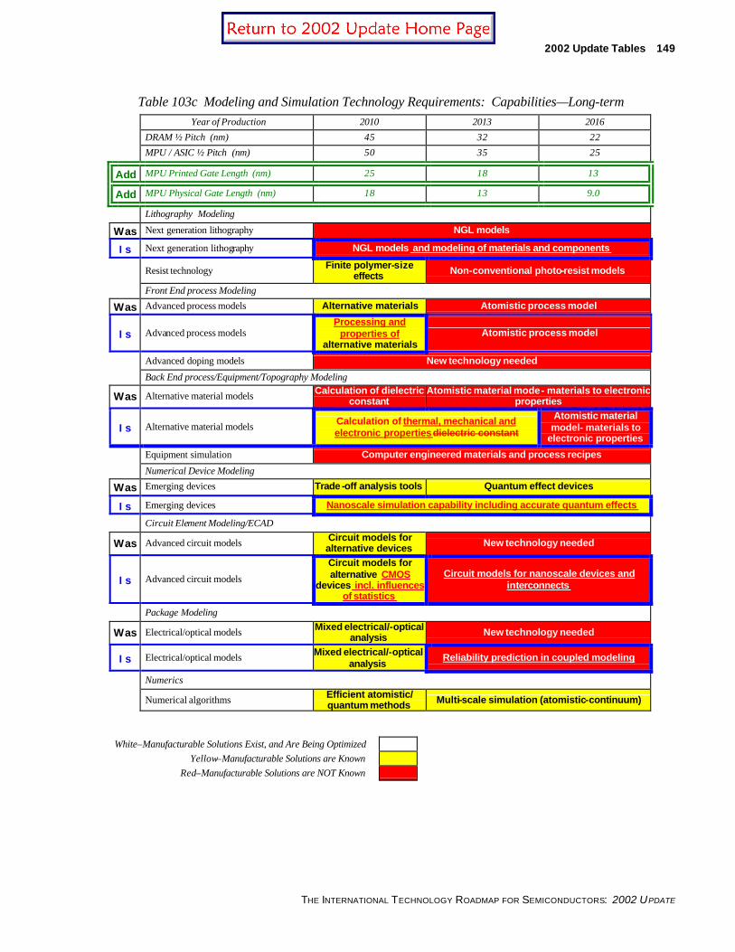
2002 Update Tables 149
THE INTERNATIONAL TECHNOLOGY ROADMAP FOR SEMICONDUCTORS: 2002 UPDATE
Table 103c Modeling and Simulation Technology Requirements: Capabilities—Long-term Year of Production 2010 2013 2016
DRAM ½ Pitch (nm) 45 32 22
MPU / ASIC ½ Pitch (nm) 50 35 25
Add MPU Printed Gate Length (nm) 25 18 13
Add MPU Physical Gate Length (nm) 18 13 9.0
Lithography Modeling
Was Next generation lithography NGL models
Is Next generation lithography NGL models and modeling of materials and components
Resist technology Finite polymer-size effects Non-conventional photo-resist models
Front End process Modeling
Was Advanced process models Alternative materials Atomistic process model
Is Advanced process models Processing and
properties of alternative materials
Atomistic process model
Advanced doping models New technology needed
Back End process/Equipment/Topography Modeling
Was Alternative material models Calculation of dielectric constant
Atomistic material model- materials to electronic properties
Is Alternative material models Calculation of thermal, mechanical and electronic properties dielectric constant
Atomistic material model- materials to
electronic properties
Equipment simulation Computer engineered materials and process recipes
Numerical Device Modeling
Was Emerging devices Trade -off analysis tools Quantum effect devices
Is Emerging devices Nanoscale simulation capability including accurate quantum effects
Circuit Element Modeling/ECAD
Was Advanced circuit models Circuit models for alternative devices New technology needed
Is Advanced circuit models
Circuit models for alternative CMOS
devices incl. influences of statistics
Circuit models for nanoscale devices and interconnects
Package Modeling
Was Electrical/optical models Mixed electrical/-optical analysis New technology needed
Is Electrical/optical models Mixed electrical/-optical analysis
Reliability prediction in coupled modeling
Numerics
Numerical algorithms Efficient atomistic/ quantum methods Multi-scale simulation (atomistic-continuum)
White–Manufacturable Solutions Exist, and Are Being Optimized Yellow–Manufacturable Solutions are Known
Red–Manufacturable Solutions are NOT Known

150 Overall Roadmap Technology Characteristics
THE INTERNATIONAL TECHNOLOGY ROADMAP FOR SEMICONDUCTORS: 2002 UPDATE
OVERALL ROADMAP TECHNOLOGY CHARACTERISTICS
BACKGROUND
The Overall Roadmap Technology Characteristics (ORTC) tables are created early in the Roadmap process and are used as the basis for initiating the activities of the International Technology Working Groups (ITWGs) in producing their detailed chapters. These tables are also used throughout the renewal effort of the Roadmap as a means of providing synchronization among the TWGs by highlighting inconsistencies between the specific tables. The process to revise the tables include increasing levels of cross-TWG and international coordination and consensus building to develop underlying models of trends and to reach agreement on target metrics. As a result, the ORTC tables went through several iterations and reviews.
The metric values of the ORTC tables can be found throughout the Roadmap in greater detail in each Technology Working Group chapter. The information in this section is intended to highlight the current rapid pace of advancement in semiconductor technology. It represents a completion of the revision update and renewal work that began in 2000. Additionally, an ORTC Glossary is provided as an appendix.
OVERVIEW OF 2001 REVISIONS
DEFINITIONS As noted above, the Overall Roadmap Technology Characteristics tables provide a consolidated summary of the key technology metrics. Please note that the year header on the tables may refer to different points in the development/life cycle of integrated circuits (ICs), depending on the individual line item metric. However, unless otherwise specified for a particular line item, the default year header still refers (as in previous Roadmaps) to the year when product shipment first exceeds 10,000 units per month of ICs from a manufacturing site using “production tooling.” Additional clarification was provided this year by the ITRS executive International Roadmap Committee (IRC), requiring a second company to start production within three months. To satisfy this definition, ASIC production may represent the cumulative volume of many individual product line items processed through the facility. Please see the Glossary section for additional details on “Technology Node” and “Production” timing definitions.
Furthermore, new IRC guidelines clarified the definition of a technology node as the achievement of significant advancement in the process technology. To be explicit, a technology node was defined as the achievement of an approximate 0.7× reduction per node (0.5× per two nodes) (Figure 5). The period of time in which a new technology node is reached is called a “technology-node cycle” (Figure 6). It is acknowledged that continuous improvement occurs between the technology nodes, and this is reflected by including data between nodes in the annual columns of the “Near-term years” tables. The “Long-term years” table columns are three-year increments of the 2001 ITRS timeframe.
ROADMAP TIMELINE
The 2001 edition of the Roadmap maintains a 15-year projection, from 2001 as a reference year and through 2016. However, the timing of future technology nodes has changed from the 1999 edition.
By international consensus, the 130 nm node was pulled in an additional year, continuing the historical precedent for two-year technology-node cycles since 350 nm/1995 (250 nm node in 1997, 180 nm node in 1999). Although there is the possibility of a continuation of the two-year-node cycle trend, the present consensus projects a three-year cycle for DRAM interconnect half-pitch nodes throughout the 2001–2016 Roadmap period (Figure 7).
DRAM interconnect (metal or polysilicon—refer to the Glossary for additional detail) half-pitch will continue to be used as the most representative feature of leading-edge semiconductor manufacturing technology for defining the achievement of a technology node. However, additional data analysis indicates an aggressive trend for the lagging MPU and ASIC interconnect half-pitches to catch up to DRAM half-pitch by 2004 (Figure 7).

Overall Roadmap Technology Characteristics 151
THE INTERNATIONAL TECHNOLOGY ROADMAP FOR SEMICONDUCTORS: 2002 UPDATE
The 2001 ITRS includes a correction of the past “rounding” convention for the technology node labels. The actual mathematical trend reduces the nodes by 50% every other node, resulting in an actual versus rounded node number targets, starting from 350 nm in 1995 as follows:
Table C Rounded versus Actual Trend Numbers
YEAR OF PRODUCTION 1995 1997 1999 2001 2004 2007 2010 2013 2016
Actual Trend Numbers (nm) 350 247.5 175 123.7 87.5 61.9 43.8 30.9 21.9
ITRS Rounded Node Numbers (nm) 350 250 180 130 90 65 45 32 22
Note the new “rounding” corrections become more critical as the industry moves into the double-digit technology nodes. Some regions, for past publication consistency, will continue to track the previous technology nodes beginning with 100 nm/2003, resulting in milestones that are placed one year earlier than the present 2001 roadmap convention (70 nm/2006; 50 nm/2009; 35nm/2012; 25 nm/2015).
The printed MPU gate length received a major correction to more an aggressive starting point in 2001. In addition, a new physical gate length is being tracked that further reduces the bottom gate length dimension of a fully-processed transistor. Both the printed and physical gate length trends are forecast to continue scaling by about 70% per two-year cycle through the 32nm physical MPU gate length in 2005, but are expected to return to a three-year cycle trend thereafter, consistent with the present DRAM half-pitch trend forecast (Figure 8).
The ORTC metrics, which guide the Roadmap, are often used by semiconductor companies as a set of targets that need to be achieved ahead of schedule to achieve industry leadership. Thus, the highly competitive environment of the semiconductor industry quickly tends to make obsolete many portions of the ORTC metrics and, consequently, the Roadmap. Hopefully, our annual update process will provide sufficiently close tracking of the evolving international consensus on technology directions to maintain the usefulness of the ITRS to the industry.
For example, there is some anticipation that DRAM half-pitch nodes could undergo an additional one-year pull-in. This possibility will be re-evaluated during the year 2002 ITRS Update process, along with the possibility of using a two-year node cycle as a longer-term trend. To reflect the variety of cycles and to allow for closer monitoring of future roadmap shifts, it was agreed to continue the practice of publishing annual technology requirements from 2001 through 2007, called the “Near-Term Years,” and at three-year (node) intervals thereafter, called the “Long-Term Years” (2010, 2013, 2016).

152 Overall Roadmap Technology Characteristics
THE INTERNATIONAL TECHNOLOGY ROADMAP FOR SEMICONDUCTORS: 2002 UPDATE
Figure 5 MOS Transistor Scaling—1974 to present
Figure 6 Scaling Calculator
MOS Transistor Scaling(1974 to present)
S=0.7[0.5x per 2 nodes]
Pitch Gate
250 -> 180 -> 130 -> 90 -> 65 -> 45 -> 32 -> 22 -> 16
0.5x
0.7x 0.7x
N N+1 N+2
Node Cycle Time (T yrs):
*CARR(T) =
[(0.5)^(1/2T yrs)] - 1
CARR(3 yrs) = -10.9%
CARR(2 yrs) = -15.9%
* CARR(T) = Compound Annual Reduction Rate
(@ cycle time period, T)
Log
Hal
f-P
itch
Linear Time
1994 NTRS -.7x/3yrs
Actual -.7x/2yrs
Scaling Calculator +Node Cycle Time:
250 -> 180 -> 130 -> 90 -> 65 -> 45 -> 32 -> 22 -> 16
0.5x
0.7x 0.7x
N N+1 N+2
Node Cycle Time (T yrs):
*CARR(T) =
[(0.5)^(1/2T yrs)] - 1
CARR(3 yrs) = -10.9%
CARR(2 yrs) = -15.9%
* CARR(T) = Compound Annual Reduction Rate
(@ cycle time period, T)
Log
Hal
f-P
itch
Linear Time
1994 NTRS -.7x/3yrs
Actual -.7x/2yrs
250 -> 180 -> 130 -> 90 -> 65 -> 45 -> 32 -> 22 -> 16
0.5x
0.7x 0.7x
N N+1 N+2
250 -> 180 -> 130 -> 90 -> 65 -> 45 -> 32 -> 22 -> 16
0.5x
0.7x 0.7x
N N+1 N+2
0.5x
0.7x 0.7x
0.5x
0.7x0.7x 0.7x0.7x
N N+1 N+2N N+1 N+2
Node Cycle Time (T yrs):
*CARR(T) =
[(0.5)^(1/2T yrs)] - 1
CARR(3 yrs) = -10.9%
CARR(2 yrs) = -15.9%
* CARR(T) = Compound Annual Reduction Rate
(@ cycle time period, T)
Log
Hal
f-P
itch
Linear Time
1994 NTRS -.7x/3yrs
Actual -.7x/2yrsL
og H
alf-
Pit
ch
Linear Time
1994 NTRS -.7x/3yrs
Actual -.7x/2yrs
Scaling Calculator +Node Cycle Time:
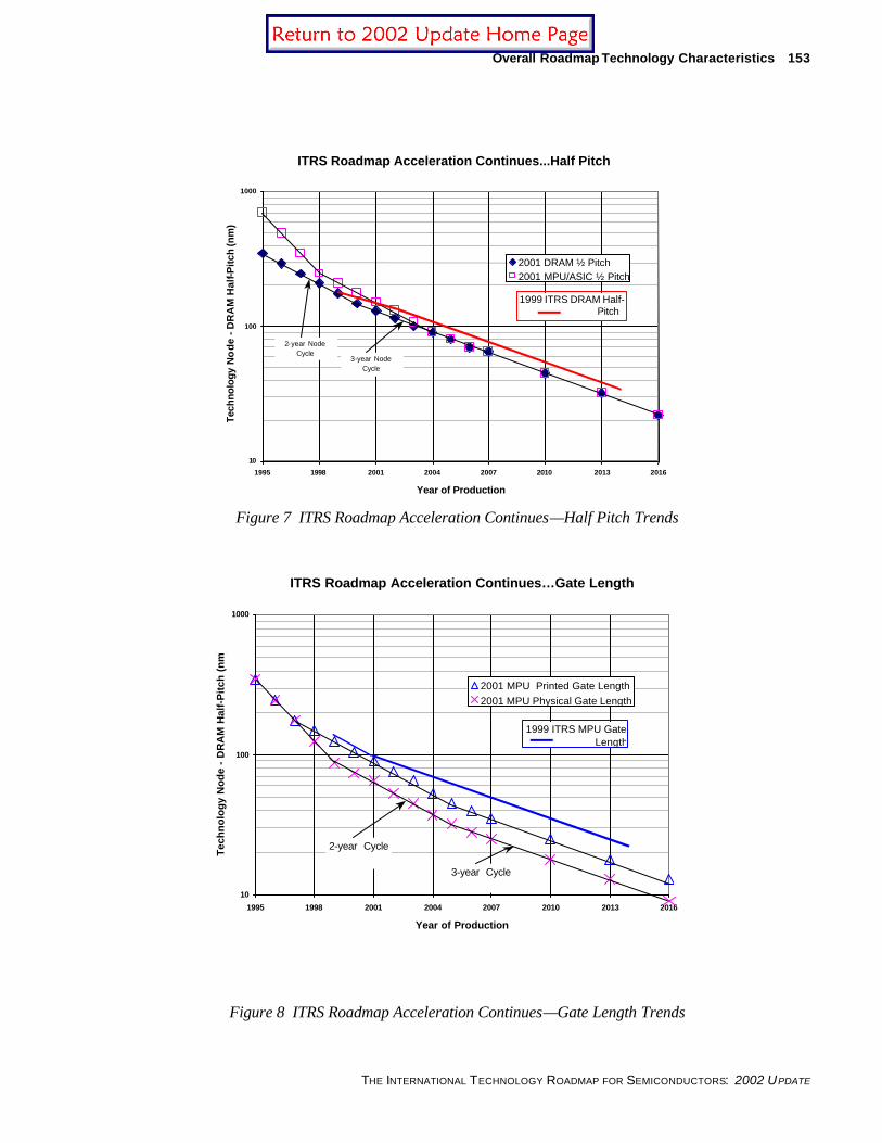
Overall Roadmap Technology Characteristics 153
THE INTERNATIONAL TECHNOLOGY ROADMAP FOR SEMICONDUCTORS: 2002 UPDATE
Figure 7 ITRS Roadmap Acceleration Continues—Half Pitch Trends
Figure 8 ITRS Roadmap Acceleration Continues—Gate Length Trends
ITRS Roadmap Acceleration Continues…Gate Length
10
100
1000
1995 1998 2001 2004 2007 2010 2013 2016
Year of Production
Tec
hn
olo
gy
No
de
- D
RA
M H
alf-
Pit
ch (
nm
)
2001 MPU Printed Gate Length2001 MPU Physical Gate Length
1999 ITRS MPU Gate-Length
2-year Cycle
3-year Cycle
ITRS Roadmap Acceleration Continues...Half Pitch
10
100
1000
1995 1998 2001 2004 2007 2010 2013 2016 Year of Production
Tech
nolo
gy N
od
e - D
RA
M H
alf-P
itch
(nm
)
2001 DRAM ½ Pitch 2001 MPU/ASIC ½ Pitch
1999 ITRS DRAM Half- Pitch
2-year Node Cycle
3-year Node Cycle

154 Overall Roadmap Technology Characteristics
THE INTERNATIONAL TECHNOLOGY ROADMAP FOR SEMICONDUCTORS: 2002 UPDATE
PRODUCT GENERATIONS AND CHIP-SIZE MODEL In this section, we will discuss “product generations” and their relationship to the technology nodes, since, in the past, these terms have often been used interchangeably. However, the historically simple picture of a new DRAM product generation every three years (at 4× the previous density and based on an essentially new set of technology features) has become obsolete as a way to define technology nodes. For this 2001 edition, the “technology node” is still linked to an anticipated DRAM feature size (minimum metal or polysilicon half-pitch). However, implications of this connection are diminishing as the product evolution/shrink path becomes more complex.
Historically, DRAM products have been recognized as the technology drivers for the entire semiconductor industry. Prior to the early 1990s, logic (as exemplified by MPU) technology was developed at a slower pace than DRAM technology. During the last few years, the development rate of new technologies used to manufacture microprocessors has accelerated. Microprocessor products are closing the half-pitch technology gap with DRAM, and are now driving the most leading-edge lithography tools and processes —especially for the capability to process the isolated-line feature of the printed and physical gate length. With this 2001 Roadmap it is recognized that DRAM and microprocessor products share the technology leadership role.
However, several fundamental differences exist between the two families of products. Due to strong commodity market economic pressure to reduce cost and increase fab output productivity, DRAM product emphasizes the minimization of the chip size. Therefore development of DRAM technology focuses mainly on minimization of the area occupied by the memory cell. However, this pressure to minimize cell size is in conflict with the requirement to maximize the capacitance of the cell for charge storage performance, which puts pressure on memory cell designers to find creative ways through design and materials to meet minimum capacitance requirements while reducing cell size. In addition, to closely pack the highest number of DRAM cells in the smallest area requires minimization of cell pitch.
Microprocessors have also come under strong market pressure to reduce costs while maximizing performance. Performance is enabled primarily by the length of the transistor gate and by the number of interconnect layers. The 2001 ITRS teams have reached consensus on models for the required functionality, chip size, cell area, and density for the ORTC tables. Additional line items were added to communicate the model consensus, and the underlying model assumptions are included in notations. Table 1a and 1b summarize the near and long technology node metrics. As agreed, the key ITRS technology node identifier would continue to be the DRAM half-pitch, but also included are the aggressive MPU gate-length performance-driven feature sizes. For completeness, the MPU/ASIC product metal half-pitch are also tracked and that will trail slightly behind or equal to the DRAM half-pitch. The ASIC/low power gate lengths are also included, and lag behind the leading-edge MPU in order to maximize standby and operating current drain. See the Glossary section for additional detail on the definition of the half-pitch and gate-length features. For each product generation, both the leading-edge (“at introduction”) and the high-volume (“at production”) DRAM products are indicated
It should be noted that the long-term average annualized reduction rate in feature size is projected to continue at approximately 11%/year (~30% reduction/three years), even though this rate accelerated to approximately 16%/year (~30% reduction/two years) in the time interval 1995–2001 (refer to Figure 5). As mentioned above, the overall schedule for introduction of a new product generation has been accelerated by one additional year.

Overall Roadmap Technology Characteristics 155
THE INTERNATIONAL TECHNOLOGY ROADMAP FOR SEMICONDUCTORS: 2002 UPDATE
Table 1a Product Generations and Chip Size Model Technology Nodes—Near-term Years
Year of Production 2001 2002 2003 2004 2005 2006 2007
DRAM ½ Pitch (nm) 130 115 100 90 80 70 65
MPU/ASIC ½ Pitch (nm) 150 130 107 90 80 70 65
MPU Printed Gate Length (nm) †† 90 75 65 53 45 40 35
MPU Physical Gate Length) (nm) 65 53 45 37 32 28 25
ASIC/Low Power Printed Gate Length (nm) †† 130 107 90 75 65 53 45
ASIC/Low Power Physical Gate Length) (nm) 90 75 65 53 45 37 32
Table 1b Product Generations and Chip Size Model Technology Nodes—Long-term years
Year of Production 2010 2013 2016
DRAM ½ Pitch (nm) 45 32 22
MPU/ASIC ½ Pitch (nm) 45 32 22
MPU Prin ted Gate Length (nm) †† 25 18 13
MPU Physical Gate Length) (nm) 18 13 9
ASIC/Low Power Printed Gate Length (nm) †† 32 22 16
ASIC/Low Power Physical Gate Length) (nm) 22 16 11
Notes for Tables 1a and 1b:
†† MPU and ASIC gate-length (in resist) node targets refer to the most aggressive requirements, as printed in photoresist (which was by definition also “as etched in polysilicon,” in the 1999 ITRS).
However, during the 2000/2001 ITRS development, trends were identified, in which the MPU and ASIC “Physical" gate lengths may be reduced from the “as-printed” dimension. These “Physical" gate-length targets are driven by the need for maximum speed performance in logic Microprocessor (MPU) products, and are included in the Front End Processes (FEP), Process Integration, Devices, and Structures (PIDs), and Design ITWG Tables as needs that drive device design and process technology requirements.
.

156 Overall Roadmap Technology Characteristics
THE INTERNATIONAL TECHNOLOGY ROADMAP FOR SEMICONDUCTORS: 2002 UPDATE
Table 1c DRAM Production Product Generations and Chip Size Model—Near-term Years Year of Production 2001 2002 2003 2004 2005 2006 2007
DRAM ½ Pitch (nm) 130 115 100 90 80 70 65
MPU/ASIC ½ Pitch (nm) 150 130 107 90 80 70 65
MPU Printed Gate Length (nm) 90 75 65 53 45 40 35
MPU Physical Gate Length (nm) 65 53 45 37 32 28 25
Cell area factor [a] 8 8 6 6 6 6 6
Cell area [Ca = a f2 ] (µm2) 0.130 0.103 0.061 0.049 0.039 0.031 0.024
Cell array area at production (% of chip size) § 54.8% 55.3% 55.7% 56.1% 56.4% 56.7% 57.0%
Generation at production § 512M 512M 1G 1G 2G 2G 4G
Functions per chip (Gbits) 0.54 0.54 1.07 1.07 2.15 2.15 4.29
Chip size at production (mm2)§ 127 100 118 93 147 116 183
Gbits/cm2 at production § 0.42 0.54 0.91 1.15 1.46 1.85 2.35
Table 1d DRAM Production Product Generations and Chip Size Model—Long-term Years Year of Production 2010 2013 2016
DRAM ½ Pitch (nm) 45 32 22
MPU/ASIC ½ Pitch (nm) 45 32 22
MPU Printed Gate Length (nm) 25 18 13
MPU Physical Gate Length (nm) 18 13 9
Cell area factor [a] 6 4 4
Cell area [Ca = a f2 ] (µm2) 0.012 0.004 0.002
Cell array area at production (% of chip size) § 57.7% 58.1% 58.4%
Generation at production § 8G 32G 64G
Functions per chip (Gbits) 8.59 34.36 68.72
Chip size at production (mm2)§ 181 239 238
Gbits/cm2 at production § 4.75 14.35 28.85
Notes for Tables 1c and 1d:
§ DRAM Model—Cell Factor (design/process improvement) targets are as follows:
1999–2002/8 ×; 2003–2010/6×; 2011–2016/4 ×.
DRAM product generations are usually increased by 4× bits/chip every four years with interim 2× bits/chip generations, except:
3. at the Introduction phase, after the 8Gbit interim generation, the introduction rate is 4×/five years (2×/two–three years); and
4. at the Production phase, after the interim 32Gbit generation, the introduction rate is 4×/five years (2×/two–three years).
InTER-generation chip size growth rate varies to maintain one chip per 572mm2 field at Introduction and two chips per 572mm2 field at Production. The more aggressive “best case opportunity” technology node trends allow the Production-phase products to remain at 2× bits/chip every two years and still fit within the target of two DRAM chips per 572mm2 field size, through the 32Gbit interim generation. The InTRA-generation chip size shrink model is 0.5× every technology node in-between cell factor reductions.
Refer to the Glossary for definitions of Introduction, Production, InTERgeneration, and InTRAgeneration terms.

Overall Roadmap Technology Characteristics 157
THE INTERNATIONAL TECHNOLOGY ROADMAP FOR SEMICONDUCTORS: 2002 UPDATE
Table 1e DRAM Introduction Product Generations and Chip Size Model—Near-term Years Year of Production 2001 2002 2003 2004 2005 2006 2007
DRAM ½ Pitch (nm) 130 115 100 90 80 70 65
MPU/ASIC ½ Pitch (nm) 150 130 107 90 80 70 65
MPU Printed Gate Length (nm) 90 75 65 53 45 40 35
MPU Physical Gate Length (nm) 65 53 45 37 32 28 25
Cell area factor [a] 8 8 6 6 6 6 6
Cell area [Ca = a f2 ] (µm2) 0.130 0.103 0.061 0.049 0.039 0.031 0.024
Cell array area at introduction (% of chip size) § 71.3% 71.8% 72.2% 72.6% 72.9% 73.2% 73.5%
Generation at introduction § 2G 2G 4G 4G 8G 8G 16G
Functions per chip (Gbits) 2.15 2.15 4.29 4.29 8.59 8.59 17.18
Chip size at introduction (mm2) § 390 308 364 287 454 359 568
Gbits/cm2 at introduction § 0.55 0.70 1.18 1.49 1.89 2.39 3.03
Table 1f DRAM Introduction Product Generations and Chip Size Model—Long-term Years Year of Production 2010 2013 2016
DRAM ½ Pitch (nm) 45 32 22
MPU/ASIC ½ Pitch (nm) 45 32 22
MPU Printed Gate Length (nm) 25 18 13
MPU Physical Gate Length (nm) 18 13 9
Cell area factor [a] 6 4 4
Cell area [Ca = a f2 ] (µm2) 0.012 0.004 0.002
Cell array area at introduction (% of chip size) § 74.2% 74.6% 74.9%
Generation at introduction § 32G 64G 64G
Functions per chip (Gbits) 34.36 68.72 68.72
Chip size at introduction (mm2) § 563 373 186
Gbits/cm2 at introduction § 6.10 18.42 37.00
Notes for Tables 1e and 1f:
§ DRAM Model—Cell Factor (design/process improvement) targets are as follows:
1999–2002/8 ×; 2003–2010/6×; 2011–2016/4 ×.
DRAM product generations are usually increased by 4× bits/chip every four years with interim 2× bits/chip generations, except:
5. at the Introduction phase, after the 8Gbit interim generation, the introduction rate is 4×/five years (2×/two–three years); and
6. at the Production phase, after the interim 32Gbit generation, the introduction rate is 4×/five years (2×/two–three years).
InTER-generation chip size growth rate varies to maintain one chip per 572mm2 field at Introduction and two chips per 572mm2 field at Production. The more aggressive “best case opportunity” technology node trends allow the Production-phase products to remain at 2× bits/chip every two years and still fit within the target of two DRAM chips per 572mm2 field size, through the 32Gbit interim generation. The InTRA-generation chip size shrink model is 0.5× every technology node in -between cell factor reductions.
Refer to the Glossary for definitions of Introduction, Production, InTERgeneration, and InTRAgeneration terms.

158 Overall Roadmap Technology Characteristics
THE INTERNATIONAL TECHNOLOGY ROADMAP FOR SEMICONDUCTORS: 2002 UPDATE
Table 1g MPU (High-volume Microprocessor) Cost-Performance Product Generations and Chip Size Model—Near-term Years
Year of Production 2001 2002 2003 2004 2005 2006 2007
DRAM ½ Pitch (nm) 130 115 100 90 80 70 65
MPU/ASIC ½ Pitch (nm) 150 130 107 90 80 70 65
MPU Printed Gate Length (nm) 90 75 65 53 45 40 35
MPU Physical Gate Length (nm) 65 53 45 37 32 28 25
SRAM Cell (6-transistor) Area factor ++ 126.1 123.0 120.3 117.8 115.6 113.7 111.9
Logic Gate (4-transistor) Area factor ++ 320.0 320.0 320.0 320.0 320.0 320.0 320.0
SRAM Cell (6-transistor) Area efficiency ++ 0.63 0.63 0.63 0.63 0.63 0.63 0.63
Logic Gate (4-transistor) Area efficiency ++ 0.50 0.50 0.50 0.50 0.50 0.50 0.50
SRAM Cell (6-transistor) Area w/overhead ++ 3.3 2.5 2.0 1.5 1.2 0.93 0.73
Logic Gate (4-transistor) Area w/overhead ++ 10.4 8.2 6.5 5.2 4.1 3.3 2.6
Transistor density SRAM (Mtransistors/cm2) 184 237 305 393 504 646 827
Transistor density logic (Mtransistors/cm2) 38.6 48.6 61.2 77.2 97.2 122.5 154.3
Generation at introduction * p04c — — p07c — — p10c
Functions per chip at introduction (million transistors [Mtransistors]) 193 243 307 386 487 614 773
Chip size at introduction (mm2) ‡ 280 280 280 280 280 280 280
Cost performance MPU (Mtransistors/cm2 at introduction) (including on-chip SRAM) ‡
69 87 110 138 174 219 276
Generation at production * p01c — — p04c — — p07c
Functions per chip at production (million transistors [Mtransistors]) 97 122 153 193 243 307 386
Chip size at production (mm2) §§ 140 140 140 140 140 140 140
Cost performance MPU (Mtransistors/cm2 at production, including on-chip SRAM) ‡
69.0 87.0 109.6 138.0 173.9 219.1 276.1
Notes for Tables 1g and 1h:
++ The MPU area factors are analogous to the "cell area factor" for DRAMs. The reduction of area factors has been achieved historically through a combination of many factors, for example—use of additional interconnect levels, self-alignment techniques, and more efficient circuit layout. However, recent data has indicated that the improvement (reduction) of the area factors is slowing, and is virtually flat for the logic gate area factor.
* p is processor, numerals reflect year of production; c indicates cost-performance product. Examples— the cost-performance processor, p01c, was introduced in 1999, but not ramped into volume production until 2001; similarly, the p04c, is introduced in 2001, but is targeted for volume production in 2004.
‡ MPU Cost-performance Model—Cost-performance MPU includes Level 2 (L2) on-chip SRAM (512Kbyte/1999), and the combination of both SRAM and logic transistor functionality doubles every technology node cycle.
§§ MPU Chip Size Model—Both the cost-performance and high-performance MPUs InTER-generation chip size growth rates are targeted to be flat through 2016, made possible by doubling the on-chip functionality every technology node cycle. The InTRA-generation chip size shrink model is 0.5× every two -year technology node through 2001, then 0.5× every three-year technology node after 2001.

Overall Roadmap Technology Characteristics 159
THE INTERNATIONAL TECHNOLOGY ROADMAP FOR SEMICONDUCTORS: 2002 UPDATE
Table 1h MPU (High-volume Microprocessor) Cost-Performance Product Generations and Chip Size Model—Long-term Years
Year of Production 2010 2013 2016
DRAM ½ Pitch (nm) 45 32 22
MPU/ASIC ½ Pitch (nm) 45 32 22
MPU Printed Gate Length (nm) 25 18 13
MPU Physical Gate Length (nm) 18 13 9
SRAM Cell (6-transistor) Area factor ++ 107.8 106.7 105.7
Logic Gate (4-transistor) Area factor ++ 320.0 320.0 320.0
SRAM Cell (6-transistor) Area efficiency ++ 0.63 0.63 0.63
Logic Gate (4-transistor) Area efficiency ++ 0.50 0.50 0.50
SRAM Cell (6-transistor) Area w/overhead ++ 0.22 0.17 0.13
Logic Gate (4-transistor) Area w/overhead ++ 0.82 0.65 0.51
Transistor density SRAM (Mtransistors/cm2) 1718 3532 7208
Transistor density logic (Mtransistors/cm2) 309 617 1235
Generation at introduction * p13c p16c p19c
Functions per chip at introduction (million transistors [Mtransistors]) 1546 3092 6184
Chip size at introduction (mm2) ‡ 280 280 280
Cost performance MPU (Mtransistors/cm2 at introduction) (including on-chip SRAM) ‡ 552 1104 2209
Generation at production * p10c p13c p16c
Functions per chip at production (million transistors [Mtransistors]) 773 1546 3092
Chip size at production (mm2) §§ 140 140 140
Cost performance MPU (Mtransistors/cm2 at production, including on-chip SRAM) ‡ 552 1104 2209
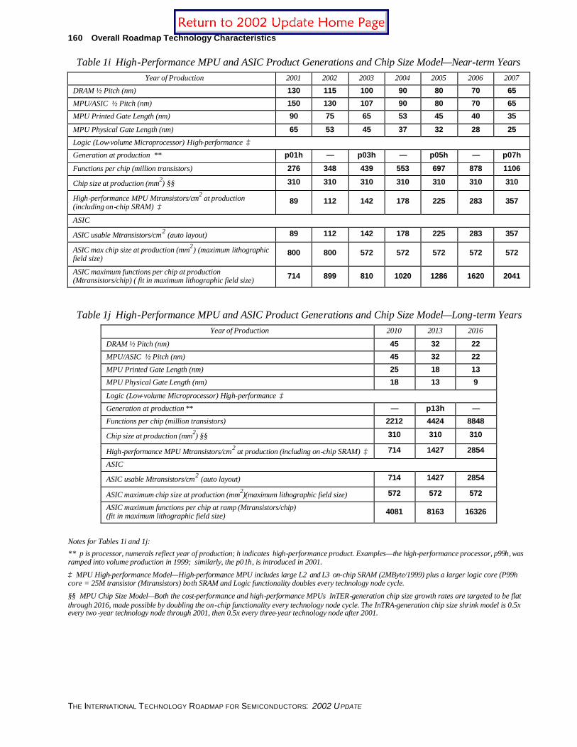
160 Overall Roadmap Technology Characteristics
THE INTERNATIONAL TECHNOLOGY ROADMAP FOR SEMICONDUCTORS: 2002 UPDATE
Table 1i High-Performance MPU and ASIC Product Generations and Chip Size Model—Near-term Years Year of Production 2001 2002 2003 2004 2005 2006 2007
DRAM ½ Pitch (nm) 130 115 100 90 80 70 65
MPU/ASIC ½ Pitch (nm) 150 130 107 90 80 70 65
MPU Printed Gate Length (nm) 90 75 65 53 45 40 35
MPU Physical Gate Length (nm) 65 53 45 37 32 28 25
Logic (Low-volume Microprocessor) High-performance ‡
Generation at production ** p01h — p03h — p05h — p07h
Functions per chip (million transistors) 276 348 439 553 697 878 1106
Chip size at production (mm2) §§ 310 310 310 310 310 310 310
High-performance MPU Mtransistors/cm2 at production (including on-chip SRAM) ‡
89 112 142 178 225 283 357
ASIC
ASIC usable Mtransistors/cm2 (auto layout) 89 112 142 178 225 283 357
ASIC max chip size at production (mm2) (maximum lithographic field size)
800 800 572 572 572 572 572
ASIC maximum functions per chip at production (Mtransistors/chip) ( fit in maximum lithographic field size) 714 899 810 1020 1286 1620 2041
Table 1j High-Performance MPU and ASIC Product Generations and Chip Size Model—Long-term Years Year of Production 2010 2013 2016
DRAM ½ Pitch (nm) 45 32 22
MPU/ASIC ½ Pitch (nm) 45 32 22
MPU Printed Gate Length (nm) 25 18 13
MPU Physical Gate Length (nm) 18 13 9
Logic (Low-volume Microprocessor) High-performance ‡
Generation at production ** — p13h —
Functions per chip (million transistors) 2212 4424 8848
Chip size at production (mm2) §§ 310 310 310
High-performance MPU Mtransistors/cm2 at production (including on-chip SRAM) ‡ 714 1427 2854
ASIC
ASIC usable Mtransistors/cm2 (auto layout) 714 1427 2854
ASIC maximum chip size at production (mm2)(maximum lithographic field size) 572 572 572
ASIC maximum functions per chip at ramp (Mtransistors/chip) (fit in maximum lithographic field size) 4081 8163 16326
Notes for Tables 1i and 1j:
** p is processor, numerals reflect year of production; h indicates high-performance product. Examples—the high-performance processor, p99h, was ramped into volume production in 1999; similarly, the p01h, is introduced in 2001.
‡ MPU High-performance Model—High-performance MPU includes large L2 and L3 on-chip SRAM (2MByte/1999) plus a larger logic core (P99h core = 25M transistor (Mtransistors) both SRAM and Logic functionality doubles every technology node cycle.
§§ MPU Chip Size Model—Both the cost-performance and high-performance MPUs InTER-generation chip size growth rates are targeted to be flat through 2016, made possible by doubling the on-chip functionality every technology node cycle. The InTRA-generation chip size shrink model is 0.5x every two -year technology node through 2001, then 0.5x every three-year technology node after 2001.

Overall Roadmap Technology Characteristics 161
THE INTERNATIONAL TECHNOLOGY ROADMAP FOR SEMICONDUCTORS: 2002 UPDATE
CHIP-SIZE, LITHOGRAPHIC-FIELD, AND WAFER-SIZE TRENDS Despite the continuous reduction in feature size of about 30% every three years, the size of first DRAM product demonstration in technical forums such as the IEEE International Solid State Circuits Conference (ISSCC) has continued to double every six years (an increase of about 12%/year). This increase in chip area has been necessary to accommodate 59% more bits/capacitors/transistors per year in accordance with Moore's Law (historically doubling functions per chip every 1.5–2 years). However, to maintain the historical trend of reducing cost/function by ~25–30%/year, it is necessary to continuously enhance equipment productivity, increase manufacturing yields, use the largest wafer size available, and, most of all, increase the number of chips available on a wafer.
The increase in the gross number of chips available on a wafer is primarily obtained by reducing the area of the chip by means of a combination of smaller feature size (shrink/scaling) and product/process redesign (compaction). For instance, using the latest models, it is forecast that the introduction chip area of a cost-effective product generation [which doubles the inter-generation (generation-to-generation) functionality every two years] must either remain flat or grow no faster than 20% every four years. Furthermore, the area must be shrunk at an intra-generation (within a generation) annual reduction rate of 50% (the square of the .7× lithography reduction rate) during every technology node period.
Affordable DRAM products must also achieve virtually flat intra -generation chip-sizes, and they must also maintain a cell area array efficiency ratio of less than 70% of total chip area. Therefore, DRAM products require aggressive cell area factors (cell area in units of minimum-feature-size-squared). The Front End Processes International Technology Working Group has provided the cell area factors and detailed the challenges and needs for solutions to meet the aggressive cell area goals in the Front End Processes chapter. Due to the importance of tracking/coordinating these new challenges, the DRAM cell area factor, the target cell sizes, and the cell array area percentage of total chip -size line items will continue to be tracked in ORTC Tables 1c, d, e, and f. (Refer to the Glossary for additional details.)
In 2001 the Design ITWG improved the MPU chip size model to update with the latest transistor densities, large on-chip SRAM, and smaller target chip sizes. The Design ITWG has also added additional detail to the model, including transistor design improvement factors. The Design ITWG notes that design improvements occur at a slow rate in SRAM transistors and very little in logic gate transistors. Almost all the “shrink” and density improvement comes from lithography-enabled interconnect half-pitch scaling alone.
The present MPU chip size model reflects additional competitive requirements for affordability and power management by targeting flat chip size trends for both high-performance MPUs (310mm2 ) and cost-performance MPUs (140mm2 ). Due to the MPU two-year-cycle half-pitch “catch-up phase” through the year 2004, the MPU products may be able to maintain flat chip sizes due to lithography improvements alone. However, after 2004, the intra-generation chip size of MPUs can remain flat only by slowing the rate of on-chip transistors to double every technology node.
Due to the forecasted return to a three-year technology node cycle, the present MPU chip-size model slows the Moore's Law rate of on-chip transistors to 2× every three years. In order to maintain a flat chip size target and also return to the historical doubling every two years of on-chip functionality (transistors), MPU chip and process designers must add additional design/process improvements to the fundamental lithography-based scaling trends. The new target metrics of the MPU model are summarized in Tables 1g, h, I, and j.
To improve productivity, it is necessary to increase the output of good chips at each step in the fabrication process. The ability of printing multiple chips in a single exposure is a key productivity driver and is determined by the field size of the lithographic tool and the size and aspect ratio of the chips being printed on the wafer. In the past, lithography exposure field sizes doubled every other technology node to meet the demand for increasing chip sizes. The result was the achievement of very large step-and-scan fields (25×32 = 800mm2) by 1999. However, the Lithography ITWG indicates that maintaining the large field size under continued reduction of exposure features is increasing costs dramatically. Therefore, the ITWG forecasts a requirement for the economically affordable lithography field to be reduced to a 572mm2 level (22×26) by the 90 nm node. That trend is shown in Tables 2a and b.
DRAM chip sizes were deemed to be the most appropriate driver of affordable lithography field sizes. In the present ITRS chip-size model for DRAMs, the introduction-level chip size is targeted to be smaller than the new affordable 572mm2 lithography field size, fitting at least one introduction-level chip size within the field. The production-level DRAM model fits at least two die within the affordable field. The combination of technology-node scaling and cell design improvements (A-factor reduction) accomplishes that goal, while also maintaining a goal of doubling on-chip bits every two years. However, the slowing of DRAM design improvements causes a requirement to add fewer on-chip bits to stay under the
162 Overall Roadmap Technology Characteristics
THE INTERNATIONAL TECHNOLOGY ROADMAP FOR SEMICONDUCTORS: 2002 UPDATE
affordable lithography field limit. This accomplished in the present DRAM model by slowing the short-term Moore's Law bits/chip rate from 2×/1.5 years to 2×/ two years. In the later years of the Roadmap the rate is stretched even more to 2×/2.5 to three years, as required. The data targets for the DRAM model are included in Tables 1c, d, e, and f.
Both the DRAM and MPU models depend upon achieving the aggressive DRAM and MPU design and process improvement targets. If those targets slip, then pressure will increase to print chip sizes larger than the present roadmap, or further slow the rate of “Moore's-Law” on-chip functionality. Either of these consequences will result in a negative impact upon cost-per-function reduction rates —the classical measure of our industries productivity-improvement and competitiveness.
With increasing cost reduction pressures, the need for the 300 mm productivity boost will also increase in urgency, especially for leading-edge manufacturers, but the poor economy will create challenges and limit capital investment. The 2001 Wafer-Diameter Generation roadmap (see Tables 2a and b) is consistent with the ramp of 300 mm capacity beginning 2001. Also, the first manufacturing capability for the next 1.5× wafer size conversion to 450 mm diameter is not anticipated to be required until 2013 in the present roadmap. However, should the other productivity-improvement drivers (lithography and design/process improvements) fail to stay on schedule, there would be a need to accelerate the use of increased wafer diameter as a productivity improvement.
The affects of future technology acceleration/deceleration and the timing of the next wafer generation conversion requires the development and application of comprehensive long-range factory productivity and industry economic models. Such industry economic modeling (IEM) work is being sponsored and carried out jointly by SEMI and International SEMATECH.

Overall Roadmap Technology Characteristics 163
THE INTERNATIONAL TECHNOLOGY ROADMAP FOR SEMICONDUCTORS: 2002 UPDATE
Table 2a Lithographic-Field and Wafer-Size Trends—Near-term Years
(Note: 2001 Lithographic field sizes represent current capability)
Year of Production 2001 2002 2003 2004 2005 2006 2007
DRAM ½ Pitch (nm) 130 115 100 90 80 70 65
MPU/ASIC ½ Pitch (nm) 150 130 107 90 80 70 65
MPU Printed Gate Length (nm) 90 75 65 53 45 40 35
MPU Physical Gate Length(nm) 65 53 45 37 32 28 25
Lithography Field Size
Lithography Field Size—area (mm2) 800 800 800 800 800 800 572
Lithographic field size — length (mm) 32 32 32 32 32 32 26
Lithographic field size — width (mm) 25 25 25 25 25 25 22
Maximum Substrate Diameter (mm) — High-volume Production (>20K wafer starts per month)
Bulk or epitaxial or SOI wafer 300 300 300 300 300 300 300
Table 2b Lithographic-Field and Wafer Size Trends—Long-term Years Year of Production 2010 2013 2016
DRAM ½ Pitch (nm) 45 32 22
MPU/ASIC ½ Pitch (nm) 45 32 22
MPU Printed Gate Length (nm) 25 18 13
MPU Physical Gate Length (nm) 18 13 9
Lithography Field Size
Maximum lithographic field size—area (mm2)
Lithography Field Size—area (mm2) 572 572 572
Maximum lithographic field size—length (mm) 26 26 26
Maximum lithographic field size—width (mm) 22 22 22
Maximum Substrate Diameter (mm)—High-volume Production (>20K wafer starts per month)
Bulk or epitaxial or SOI wafer 300 450 450

164 Overall Roadmap Technology Characteristics
THE INTERNATIONAL TECHNOLOGY ROADMAP FOR SEMICONDUCTORS: 2002 UPDATE
PERFORMANCE OF PACKAGED CHIPS
NUMBER OF PADS AND PINS / PAD PITCH, COST PER PIN, FREQUENCY
The demand for a higher number of functions on a single chip requires the integration of an increased number of transistors or bits (memory cells) for each product generation. Typically, the number of pads and pins necessary to allow Input/Output (I/O) signals to flow to and from an integrated circuit increases as the number of transistors on a chip increases. (Refer to Tables 3a and b)
Additional power and ground connections to the chip are also necessary to optimize power management and to increase noise immunity. Based upon chip pad-count numbers supplied by the Test ITWG, logic products (MPUs and high-performance ASICs) both approach 4-6K pads over the ITRS period. The MPU products are forecast to increase the total number of pads through this period by nearly 50%, and the ASICs double the maximum number of pads per chip. The two product types also differ significantly in the ratio of power/ground pads. The MPU product pad counts typically have 1:3 signal I/O pads and 2:3 power and ground pads, or two power/ground pads for every signal I/O pad. Unlike MPUs, high-performance ASIC product pad counts typically include one power/ground pad for each signal I/O pad.
Table 3a Performance of Packaged Chips: Number of Pads and Pins—Near-term Years Year of Production 2001 2002 2003 2004 2005 2006 2007
DRAM ½ Pitch (nm) 130 115 100 90 80 70 65
MPU/ASIC ½ Pitch (nm) 150 130 107 90 80 70 65
MPU Printed Gate Length (nm) 90 75 65 53 45 40 35
MPU Physical Gate Length (nm) 65 53 45 37 32 28 25
Number of Chip I/Os (Number of Total Chip Pads) — Maximum
Total pads—MPU 3072 3072 3072 3072 3072 3072 3072
Signal I/O—MPU (1/3 of total pads) 1024 1024 1024 1024 1024 1024 1024
Power and ground pads—MPU (2/3 of total pads)
2048 2048 2048 2048 2048 2048 2048
Total pads—ASIC high-performance 3000 3200 3400 3600 4000 4200 4400
Signal I/O pads—ASIC high-performance 1500 1600 1700 1800 2000 2100 2200
Power and ground pads—ASIC high-performance (½ of total pads)
1500 1600 1700 1800 2000 2100 2200
Number of Total Package Pins—Maximum [1]
Microprocessor/controller, cost-performance 480–1,200 480–1320 500–1452 500–1600 550–1760 550–1936 600–2140
Microprocessor/controller, high-performance 1200 1320 1452 1,600 1,760 1,936 2,140
ASIC (high-performance) 1700 1870 2057 2263 2489 2738 3012
Notes for Tables 3a and 3b:
[1] Pin counts will be limited for some applications where fine pitch array interconnect is used by PWB technology and system cost.
The highest pin count applications will as a result use larger pitches and larger package sizes.
The reference to signal pin ratio will also vary greatly dependent on applications with an expected range from 2:1 to 1:4

Overall Roadmap Technology Characteristics 165
THE INTERNATIONAL TECHNOLOGY ROADMAP FOR SEMICONDUCTORS: 2002 UPDATE
Table 3b Performance of Packaged Chips: Number of Pads and Pins—Long-term Years Year of Production 2010 2013 2016
DRAM ½ Pitch (nm) 45 32 22
MPU/ASIC ½ Pitch (nm) 45 32 22
MPU Printed Gate Length (nm) 25 18 13
MPU Physical Gate Length (nm) 18 13 9
Number of Chip I/Os (Number of Total Chip Pads) — Maximum
Total pads—MPU 3840 4224 4416
Signal I/O—MPU (1/3 of total pads) 1280 1408 1472
Power and ground pads—MPU (2/3 of total pads) 2560 2816 2944
Total pads—ASIC high-performance 4800 5400 6000
Signal I/O pads—ASIC high-performance 2400 2700 3000
Power and ground pads—ASIC high-performance (½ of total pads) 2400 2700 3000
Number of Total Package Pins—Maximum [1]
Microprocessor/controller, cost-performance 780–2782 1014–3616 1318–4702
Microprocessor/controller, high-performance 2782 3616 4702
ASIC (high-performance) 4009 5335 7100
Package pin count (Tables 3 a and b) and cost-per-pin (Tables 4 a and b ), provided by the Assembly and Packaging ITWG, point out challenges to future manufacturing economics. Based upon the projected growth in the number of transistors/chip, it is forecast that the number of package pin/balls will continue to grow at an annual rate of approximately 10%, while the cost/pin decreases at 5%/year. These trends make it more challenging for suppliers of packaging technologies to deliver cost-effective solutions, because the overall average cost of packaging will increase annually at 5%/year (.95 cost/pin × 1.10 pins/year = 1.05 cost/year).
In the very competitive consumer electronics product environment, prices for high-volume, high-tech products such as PCs and cell phones tend to remain flat or even decrease. These same high-tech products typically also deliver twice the performance every two years. This is the end-use market environment of the leading-edge semiconductor manufacturer, and it is the fundamental economic driver behind the ITRS economic requirement to reduce cost per function (bits, transistors) at an annual 30% or faster rate (2× functionality/chip at flat price every two years = 29%/year).
If future semiconductor component products must be targeted to maintain constant or decreasing prices and the average number of pins per unit increases at 10% while the average cost per pin decreases at only 5%, then the following will occur:
1. the average packaging share of total product cost will double over the 15-year roadmap period, and 2. the ultimate result will be greatly reduced gross profit margins and limited ability to invest in R&D and factory
capacity.
This conclusion is one of the drivers behind the industry trends to reduce the overall system pin requirements by combining functionality into Systems -on-Chip (SoC) and through the use of multi-chip modules, bumped chip-on-board (COB), and other creative solutions.
In addition to the need to increase functionality while exponentially decreasing cost per function, there is also a market demand for higher-performance, cost-effective products. Just as Moore’s Law predicts that functions-per-chip will double every 1.5–2 years to keep up with consumer demand, there is a corresponding demand for processing electrical signals at progressively higher rates. In the case of MPUs, processor instructions/second have also historically doubled every 1.5–2 years. For MPU products, increased processing power, measured in millions of instructions per second (MIPs), is accomplished through a combination of “raw technology performance” (clock frequency) multiplied by “architectural performance” (instructions per clock cycle). The need for a progressively higher operational frequency associated with an

166 Overall Roadmap Technology Characteristics
THE INTERNATIONAL TECHNOLOGY ROADMAP FOR SEMICONDUCTORS: 2002 UPDATE
increasing average chip size will continue to demand the development of novel process, design, and packaging techniques.
These considerations are reflected in Tables 4c and d, which includes line items contributed by the Design and Assembly and Packaging ITWGs to forecast the maximum on-chip and chip-to-board frequency trends. The highest frequency obtainable in each product generation is directly related to the intrinsic transistor performance (on-chip, local clock). The difference between this “local” frequency and the frequency of signals traveling across the chip increases due to degradation of signal propagation delay caused by line-to-line and line-to-substrate capacitive coupling. Additional signal degradation is associated with the inductance of wire bonds and package leads. Direct chip attachment may eventually be the only viable way to eliminate any parasitic effect introduced by the package. To optimize signal and power distribution across the chip, it is expected that the number of layers of interconnect will continue to increase. As size downscaling of interconnect also continues, wider use of copper (low resistivity) and various inter-metal insulating materials of progressively lower dielectric constant (κ~2–3) will be adopted in the chip fabrication process. Multiplexing techniques will also be used to increase the chip-to-board operating frequency (off-chip).
Table 4a Performance and Package Chips: Pads, Cost—Near-term Years [Update] Year of Production 2001 2002 2003 2004 2005 2006 2007
DRAM ½ Pitch (nm) 130 115 100 90 80 70 65
MPU/ASIC ½ Pitch (nm) 150 130 107 90 80 70 65
MPU Printed Gate Length (nm) 90 75 65 53 45 40 35
MPU Physical Gate Length (nm) 65 53 45 37 32 28 25
Chip Pad Pitch (micron)
Was Pad pitch—ball bond 45 35 30 25 20 20 20
Is Pad pitch—ball bond 45 40 35 30 25 20 20
Was Pad pitch—wedge bond 40 35 30 25 20 20 20
Is Pad pitch—wedge bond 50 50 40 40 35 35 30
Was Pad Pitch—area array flip-chip (cost-performance, high-performance) 160 160 150 150 130 130 120
Is Pad Pitch—area array flip-chip (cost-performance, high-performance) 200 180 150 150 100 100 80
Was Pad Pitch—peripheral flip-chip (handheld, low-cost, harsh) 150 130 120 110 100 90 80
Is Pad Pitch—peripheral flip-chip (handheld, low-cost, harsh) 80 80 60 60 40 40 30
Cost-Per-Pin
Was Package cost (cents/pin) (cost-performance)— minimum–maximum 0.80–1.60 0.75–1.44 0.70–1.30 0.66–1.17 0.61–1.06 0.56–1.03 0.64–1.00
Is Package cost (cents/pin) (cost-performance)— minimum–maximum
0.80–1.60
0.75–1.30
0.70–1.24
0.66–1.17
0.61–1.11
0.56–1.06
0.64–1.01
Package cost (cents/pin) (Memory)—minimum–maximum 0.36–1.54 0.34–1.39 0.32–1.26 0.30–1.14 0.28–1.03 0.27–0.93 0.27–0.84

Overall Roadmap Technology Characteristics 167
THE INTERNATIONAL TECHNOLOGY ROADMAP FOR SEMICONDUCTORS: 2002 UPDATE
Table 4b Performance and Package Chips: Pads, Cost—Long-term Years [Update] Year of Production 2010 2013 2016
DRAM ½ Pitch (nm) 45 32 22
MPU/ASIC ½ Pitch (nm) 45 32 22
MPU Printed Gate Length (nm) 25 18 13
MPU Physical Gate Length (nm) 18 13 9
Chip Pad Pitch (micron)
Pad pitch—ball bond 20 20 20
Pad Pitch—wedge bond 20 20 20
Was Pad Pitch—area array (cost-performance, high-performance) 90 80 70
Is Pad Pitch—area array (cost-performance, high-performance) 70 70 50
Was Pad Pitch—peripheral flip-chip (handheld, low-cost, harsh) 60 45 30
Is Pad Pitch—peripheral flip-chip (handheld, low-cost, harsh) 20 20 15
Cost-Per-Pin
Package cost (cents/pin) (cost-performance)— minimum–maximum 0.49–0.980.42–0.930.36–0.79
Package cost (cents/pin) (Memory)— minimum–maximum 0.22–0.540.19–0.390.19–0.33
Table 4c Performance and Package Chips: Frequency On-Chip Wiring Levels—Near-term Years [Update] YEAR OF PRODUCTION 2001 2002 2003 2004 2005 2006 2007 DRAM ½ Pitch (nm) 130 115 100 90 80 70 65
MPU/ASIC ½ Pitch (nm) 150 130 107 90 80 70 65
MPU Printed Gate Length (nm) 90 75 65 53 45 40 35
MPU Physical Gate Length (nm) 65 53 45 37 32 28 25
Chip Frequency (MHz)
On-chip local clock 1,684 2,317 3,088 3,990 5,173 5,631 6,739
Chip-to-board (off-chip) speed (high-performance, for peripheral buses)[1] 1,684 2,317 3,088 3,990 5,173 5,631 6,739
Was Maximum number wiring levels—maximum 7 8 8 8 9 9 9
Is Maximum number wiring levels—maximum 10 10 12 13 14 14 14
Was Maximum number wiring levels—minimum 7 7 8 8 8 9 9
Is Maximum number wiring levels—maximum 10 10 12 9 10 10 10

168 Overall Roadmap Technology Characteristics
THE INTERNATIONAL TECHNOLOGY ROADMAP FOR SEMICONDUCTORS: 2002 UPDATE
Table 4d Performance and Package Chips: Frequency, On-Chip Wiring Levels—Long-term Years [Update] Year of Production 2010 2013 2016
DRAM ½ Pitch (nm) 45 32 22
MPU/ASIC ½ Pitch (nm) 45 32 22
MPU Printed Gate Length (nm) 25 18 13
MPU Physical Gate Length (nm) 18 13 9
Chip Frequency (MHz)
On-chip local clock 11,511 19,348 28,751
Chip-to-board (off-chip) speed (high-performance, for peripheral buses)[1] 11,511 19,348 28,751
Was Maximum number wiring levels—maximum 10 10 10
Is Maximum number wiring levels—maximum 14 15 15
Was Maximum number wiring levels—minimum 9 9 10
Is Maximum number wiring levels—minimum 10 11 11
Note for Ta bles 4c and 4d:
[1] The off chip frequency is expected to increase for a small number of high speed pins which will be used in combination with a large number of lower speed pins
[2] In 2001, high-speed serial communications transceiver devices are achieving chip-board frequencies of 3.125 GHz using CMOS, and 10 GHz using SiGe. In 2002 it is expected that 10 GHz transceivers will be fabricated using CMOS. 40 GHz SiGe devices are expected in 2003. The roadmap for higher levels of integration with wider bus widths, is shown in the High Frequency Serial Communications section in the Test chapter.
Add [3] The Minimum number of wiring levels represents the Interconnect metal levels, and the Maximum number of Interconnect wiring levels includes the Minimum number of wiring levels plus additional optional levels required for power, ground, signal conditioning, and integrated passives (i.e., capacitors).

Overall Roadmap Technology Characteristics 169
THE INTERNATIONAL TECHNOLOGY ROADMAP FOR SEMICONDUCTORS: 2002 UPDATE
ELECTRICAL DEFECT DENSITY The latest targets for electrical defect density of DRAM, MPU, and ASIC (necessary to achieve 83–89.5 % chip yield in the year of volume production) are shown in Tables 5a and b. The allowable number of defects is calculated by taking into account the different chip sizes based on the latest chip size model forecasts, as reported in Table 1 for DRAM and microprocessors . In addition, the data in the table are now reported only at the production-level of the product life -cycle. Other defect densities may be calculated at different chip sizes at the same technology node by using the formula found in the Yield Enhancement chapter. The approximate number of masks for logic devices is included as an indicator of the ever-increasing process complexity.
Table 5a Electrical Defects—Near-term Years Year of Production 2001 2002 2003 2004 2005 2006 2007
DRAM ½ Pitch (nm) 130 115 100 90 80 70 65
MPU/ASIC ½ Pitch (nm) 150 130 107 90 80 70 65
MPU Printed Gate Length (nm) 90 75 65 53 45 40 35
MPU Physical Gate Length (nm) 65 53 45 37 32 28 25
DRAM Random Defect D0 at production chip size and 89.5% yield (faults/m2) §
1,963 2,493 2,148 2,748 1,752 2236 1426
MPU Random Defect D0 at production chip size and 83% yield (faults/m2) §§
1,356 1,356 1,356 1,356 1,356 1,356 1,356
# Mask Levels – MPU 25 25 25 25 25 27 27
# Mask Levels – DRAM 21 22 24 24 24 24 24
Table 5b Electrical Defects—Long-term Years Year of Production 2010 2013 2016
DRAM ½ Pitch (nm) 45 32 22
MPU/ASIC ½ Pitch (nm) 45 32 22
MPU Printed Gate Length (nm) 25 18 13
MPU Physical Gate Length (nm) 18 13 9
DRAM Random Defect D0 at production chip size and 89.5% yield (faults/m2) §
1356 1356 1356
MPU Random Defect D0 at production chip size and 83% yield (faults/m2) §§
1464 1116 1134
# Mask Levels – MPU 27 29 29
# Mask Levels – DRAM 26 26 26
Notes for Tables 5a and 5b: D0 — defect density
§ DRAM Model—Cell Factor (design/process improvement) targets are as follows:
1999–2002/8 ×; 2003–2010/6×; 2011–2016/4 ×.
DRAM product generations are usually increased by 4× bits/chip every four years with interim 2× bits/chip generations, except:
1. at the Introduction phase, after the 8Gbit interim generation, the introduction rate is 4×/five years (2×/two–three years); and
2. at the Production phase, after the interim 32Gbit generation, the introduction rate is 4×/five years (2×/two–three years).
InTER-generation chip size growth rate varies to maintain one chip per 572mm2 field at Introduction and two chips per 572mm2 field at Production. The more aggressive “best case opportunity” technology node trends allow the Production-phase products to remain at 2× bits/chip every two years and still fit within the target of two DRAM chips per 572mm2 field size, through the 32Gbit interim generation. The InTRA-generation chip size shrink model is 0.5× every technology node in-between cell factor reductions.
Refer to the Glossary for definitions of Introduction, Production, InTERgeneration, and InTRAgeneration terms. §§ MPU Chip Size Model—Both the cost-performance and high-perfo rmance MPUs InTER-generation chip size growth rates are targeted to be flat through 2016, made possible by doubling the on-chip functionality every technology node cycle. The InTRA-generation chip size shrink model is 0.5× every two -year technology node through 2001, then 0.5× every three-year technology node after 2001.

170 Overall Roadmap Technology Characteristics
THE INTERNATIONAL TECHNOLOGY ROADMAP FOR SEMICONDUCTORS: 2002 UPDATE
POWER SUPPLY AND POWER DISSIPATION Reduction of power supply voltage (see Tables 6a and b) is driven by several factors—reduction of power dissipation, reduced transistor channel length, and reliability of gate dielectrics. As seen in Tables 6a and b, the value of the power supply voltage is now given as a range.
Selection of a specific Vdd value continues to be a part of the analysis undertaken to simultaneously optimize speed and power for an IC, leading to a range of usable power supply voltages in each product generation. Values of Vdd as low as 0.5 volts are expected to be achieved by 2013, but the lowest target is now 0.4V by 2016 (versus 0.3V by 2014 in the 1999 ITRS).
Maximum power trends (e.g., for MPUs) are presented in three categories—1) high-performance desktop applications, for which a heat sink on the package is permitted; 2) cost-performance, where economical power management solutions of the highest performance are most important; and 3) portable battery operations. In all cases, total power consumption continues to increase, despite the use of a lower supply voltage. The increased power consumption is driven by higher chip operating frequencies, the higher interconnect overall capacitance and resistance; and the increasing gate leakage of exponentially-growing and scaled on-chip transistors.
Table 6a Power Supply and Power Dissipation—Near-term Years Year of Production 2001 2002 2003 2004 2005 2006 2007
DRAM ½ Pitch (nm) 130 115 100 90 80 70 65
MPU/ASIC ½ Pitch (nm) 150 130 107 90 80 70 65
MPU Printed Gate Length (nm) 90 75 65 53 45 40 35
MPU Physical Gate Length (nm) 65 53 45 37 32 28 25
Power Supply Voltage (V)
Vdd (high performance) 1.1 1.0 1.0 1 0.9 0.9 0.7
Vdd (Low Operating Power, high Vdd transistors) 1.2 1.2 1.1 1.1 1.0 1.0 0.9
Vdd (Low Standby Power, high Vdd transistors) 1.2 1.2 1.2 1.2 1.2 1.2 1.1
Allowable Maximum Power [1]
High-performance with heatsink (W) 130 140 150 160 170 180 190
Cost-performance (W) 61 75 81 85 92 98 104
Battery (W)—(hand-held) 2.4 2.6 2.8 3.2 3.2 3.5 3.5
Table 6b Power Supply and Power Dissipation—Long-term Years
Year of Production 2010 2013 2016
DRAM ½ Pitch (nm) 45 32 22
MPU/ASIC ½ Pitch (nm) 45 32 22
MPU Printed Gate Length (nm) 25 18 13
MPU Physical Gate Length (nm) 18 13 9
Power Supply Voltage (V)
Vdd (high performance) 0.6 0.5 0.4
Vdd (Low Operating Power, high Vdd transistors) 0.8 0.7 0.6
Vdd (Low Standby Power, high Vdd transistors) 1.0 0.9 0.9
Allowable Maximum Power [1]
High-performance with heatsink (W) 218 251 288
Cost-performance (W) 120 138 158
Battery (W)—(hand-held) 3.0 3.0 3.0
Note for Table 6a and 6b: [1] Power will be limited more by system level cooling and test constraints than packaging

Overall Roadmap Technology Characteristics 171
THE INTERNATIONAL TECHNOLOGY ROADMAP FOR SEMICONDUCTORS: 2002 UPDATE
COST Tables 7a and b are dedicated to cost trends. The ability to reduce the cost per function by an average 25–30% each year represents one of the unique features of the semiconductor industry and is a direct consequence of the market pressure to continue to deliver twice the functionality on-chip every 1.5–2 years in an environment of constant or reducing prices. In support of this cost reduction, a continuously increasing amount of investment is needed for R&D and manufacturing capital. Even on a per-factory basis, the capital cost of manufacturing continues to escalate. Yet, the semiconductor industry has historically delivered two times as many functions per chip every 1.5–2 years with no or only a moderate increase in chip size and cost (approximately constant cost per cm2 of silicon). This technological and economic performance is the fundamental engine behind the growth of the semiconductor industry.
However, the customers in today’s competitive market environment are resistant to even “moderate” increases in cost and the rate of doubling functions per chip (Moore’s Law) is slowing. Therefore, the semiconductor manufacturers must seek a new model to deliver the same cost-per-function reduction requirements that have fueled industry growth. Consequently, the 1999 ITRS proposed a new model for achieving the required reduction: provide the customer twice the functionality every two years at a constant cost and average selling price (ASP) per chip. The 2001 ITRS uses the model and results in the same 29% cost reduction of a function (bit, transistor, etc.) that has been achieved historically by delivering four times the functionality per chip every three years at 1.4× increase in cost per unit. The DRAM and MPU cost models continue to use the need for that 29% cost-per-function productivity reduction rate as an economic driver of the industry. Therefore, that core cost-per-function trend has been used to set the INTRA-generation trends for the affordable cost/bit and cost/transistor for DRAM and microprocessors, respectively. Extrapolation of historical trends would indicate an “at introduction” affordable cost/bit of approximately 21 microcents for 2-Gbit DRAMs in 2001. In addition, the historical trends indicate that, within a DRAM generation, a 45%/year reduction in cost/bit should be expected.2 A corresponding analysis conducted from published data for microprocessors yields similar results.3 As a result the 29%/year target for reduction in affordable cost/transistor from generation to generation is also being used in the MPU model , along with the 45%/year reduction rate within the same generation.
However, the Design ITWG has updated the MPU model, based upon recent data. The new data indicates that logic transistor size is improving only at the rate of the lithography (0.7× linear, 0.5×area reduction every technology node). Therefore in order to keep the MPU chip sizes flat, the number of transistors can be doubled only every technology node. The technology node rate is projected to return to a three-year cycle after 2001, therefore the transistors per MPU chip can double only every three years after 2001. DRAM memory bit cell design improvements are also slowing down, and the rate of bits per chip will also be slowing in the future to keep chip sizes under control. To compensate for slowing DRAM and MPU functions-per-chip, there will be increasing pressure to find alternative productivity enhancements from the equivalent productivity scaling benefits of chip and system-level architecture and designs.
Even though the rate of increase of on-chip functionality could slow in the future, the amount of functions/chip is still growing exponentially. As the number of functions/chip continues to increase, it becomes increasingly difficult and, therefore, costly to test the final products. This is reflected in the escalating cost of testers. Even though the cost/pin of testers is forecast to decline between 0% and 10% per year (Tables 7 a and b), the number of pins grows at 10%year (Tables 4 a and b). Therefore, the need for accelerated implementation of Built-In -Self-Test (BIST) and Design-For-Testability (DFT) techniques will continue within the time frame of the 2001 International Technology Roadmap for Semiconductors. Further discussion is detailed in the Test chapter.
2 McClean, William J., ed. Mid-Term 1994: Status and Forecast of the IC Industry . Scottsdale: Integrated Circuit Engineering Corporation, 1994. McClean, William J., ed. Mid-Term 1995: Status and Forecast of the IC Industry . Scottsdale: Integrated Circuit Engineering Corporation, 1995. 3 a) Dataquest Incorporated. x86 Market: Detailed Forecast, Assumptions, and Trends. MCRO–WW–MT–9501. San Jose: Dataquest Incorporated, January 16, 1995. b) Port, Otis; Reinhardt, Andy; McWilliams, Gary; and Brull, Steven V. "The Silicon Age? It's Just Dawning," Table 1. Business Week, December 9, 1996, 148–152.

172 Overall Roadmap Technology Characteristics
THE INTERNATIONAL TECHNOLOGY ROADMAP FOR SEMICONDUCTORS: 2002 UPDATE
Table 7a Cost—Near-term Years Year of Production 2001 2002 2003 2004 2005 2006 2007
DRAM ½ Pitch (nm) 130 115 100 90 80 70 65
MPU/ASIC ½ Pitch (nm) 150 130 107 90 80 70 65
MPU Printed Gate Length (nm) 90 75 65 53 45 40 35
MPU Physical Gate Length (nm) 65 53 45 37 32 28 25
Affordable Cost per Function ++
DRAM cost/bit at (packaged microcents) at samples/introduction 21 14.8 10.5 7.4 5.3 3.7 2.6
DRAM cost/bit at (packaged microcents) at production § 7.7 5.4 3.8 2.7 1.9 1.4 0.96
Cost-performance MPU (microcents/transistor) (including on-chip SRAM) at introduction §§ 176 124 88 62 44 31 22
Cost-performance MPU (microcents/transistor) (including on-chip SRAM) at production §§ 107 75 53 38 27 19 13.3
High-performance MPU (microcents/transistor) (including on-chip SRAM) at production §§ 97 69 49 34 24 17 12
Cost-Per-Pin
Test Cost
Volume tester cost per high-frequency signal pin ($K/pin) (high-performance ASIC) —maximum 4.0 3.0 3.0 3.0 3.0 3.0 3.0
Volume tester cost per high-frequency signal pin ($K/pin) (high-performance ASIC) —minimum 1.0 1.0 1.0 1.0 1.0 1.0 1.0
Notes for Tables 7a and 7b:
++ Affordable packaged unit cost per function based upon Average Selling Prices (ASPs) available from various analyst reports less Gross Profit Margins (GPMs); 35% GPM used for commodity DRAMs and 60% GPM used for MPUs; 0.5×/two years inTER-generation reduction rate model used; .55×/year inTRA-generation reduction rate model used; DRAM unit volume life-cycle peak occurs when inTRA-generation cost per function is crossed by next generation, typically seven–eight years after introduction; MPU unit volume life-cycle peak occurs typically after four–six years, when the next generation processor enters its ramp phase (typically two -four years after introduction).
§ DRAM Model—Cell Factor (design/process improvement) targets are as fo llows: 1999–2002/8 ×; 2003–2010/6×; 2011–2016/4 ×. DRAM product generations are usually increased by 4× bits/chip every four years with interim 2× bits/chip generations, except:
1) at the Introduction phase, after the 8Gbit interim generation, the introduction rate is 4×/five years (2×/two–three years); and
2) at the Production phase, after the interim 32Gbit generation, the introduction rate is 4×/five years (2×/two–three years).
InTER-generation chip size growth rate varies to maintain one chip per 572mm2 field at Introduction and two chips per 572mm2 field at Production. The more aggressive “best case opportunity” technology node trends allow the Production-phase products to remain at 2× bits/chip every two years and still fit within the target of two DRAM chips per 572mm2 field size, through the 32Gbit interim generation. The InTRA-generation chip size shrink model is 0.5× every technology node in-between cell factor reductions.
Refer to the Glossary for definitions of Introduction, Production, InTERgeneration, and InTRAgeneration terms. §§ MPU Chip Size Model—Both the cost-performance and high-performance MPUs InTER-generation chip size growth rates are targeted to be flat through 2016, made possible by doubling the on-chip functionality every technology node cycle. The InTRA-generation chip size shrink model is 0.5× every two -year technology node through 2001, then 0.5× every three-year technology node after 2001.

Overall Roadmap Technology Characteristics 173
THE INTERNATIONAL TECHNOLOGY ROADMAP FOR SEMICONDUCTORS: 2002 UPDATE
Table 7b Cost—Long-term Years Year of Production 2010 2013 2016
DRAM ½ Pitch (nm) 45 32 22
MPU/ASIC ½ Pitch (nm) 45 32 22
MPU Printed Gate Length (nm) 25 18 13
MPU Physical Gate Length (nm) 18 13 9
Affordable Cost per Function ++
DRAM cost/bit (packaged microcents) at samples/introduction 0.93 0.33 0.12
DRAM cost/bit (packaged microcents) at production § 0.34 0.12 0.042
Cost-performance MPU (microcents/transistor) (including on-chip SRAM) at introduction §§ 7.78 2.75 0.97
Cost-performance MPU (microcents/transistor) (including on-chip SRAM) at production §§ 4.71 1.66 0.59
High-performance MPU (microcents/transistor) (including on-chip SRAM) at production §§ 4.31 1.52 0.54
Cost-Per-Pin
Test Cost
Volume tester cost per high-frequency signal pin ($K/pin) (high-performance ASIC)—maximum 4 4 4
Volume tester cost per high-frequency signal pin ($K/pin) (high-performance ASIC)—minimum 2 3 4
174 Glossary
THE INTERNATIONAL TECHNOLOGY ROADMAP FOR SEMICONDUCTORS: 2002 UPDATE
GLOSSARY KEY ROADMAP TECHNOLOGY CHARACTERISTICS TERMINOLOGY (WITH OBSERVATIONS AND ANALYSIS)
CHARACTERISTICS OF MAJOR MARKETS Technology Node—The ground rules of process governed by the smallest feature printed. The half-pitch of first-level interconnect dense lines is most representative of the DRAM technology level required for the smallest economical chip size. For logic, such as microprocessors (MPUs), physical bottom gate length is most representative of the leading-edge technology level required for maximum performance. MPU and ASIC logic interconnect half-pitch processing requirement typically refers to the first polysilicon or metal layer and lags behind DRAM half-pitch, which may also refer either first layer metal or polysilicon. The smallest half-pitch is typically found in the memory cell area of the chip. Each technology node step represents the creation of significant technology progress—approximately 70% of the preceding node, 50% of two preceding nodes. Example: DRAM half pitches of 180, 130, 90, 65, 45, 32 nm, and 22 nm. For cost reasons, high-volume, low-cost ASIC gate-length requirements will typically match DRAM half-pitch targets, but the low-volume leading-edge high-performance ASIC gate-length requirements will track closely with MPUs.
Moore’s Law—An historical observation by Intel executive, Gordon Moore, that the market demand (and semiconductor industry response) for functionality per chip (bits, transistors) doubles every 1.5 to 2 years. He also observed that MPU performance [clock frequency (MHz) × instructions per clock = millions of instructions per second (MIPS)] also doubles every 1.5 to 2 years. Although viewed by some as a “self-fulfilling” prophecy, “Moore's Law” has been a consistent macro trend and key indicator of successful leading-edge semiconductor products and companies for the past 30 years.
Cost-per-Function Manufacturing Productivity Improvement Driver—In addition to Moore’s Law, there is a historically-based “corollary” to the “law,” which suggests that to be competitive manufacturing productivity improvements must also enable the cost-per-function (microcents per bit or transistor) to decrease by -29% per year. Historically, when functionality doubled every 1.5 years, then cost-per-chip (packaged unit) could double every six years and still meet the cost-per-function reduction requirement. If functionality doubles only every two years, as suggested by consensus DRAM and MPU models of the 1999 ITRS, then the manufacturing cost per chip (packaged unit) must remain flat.
Affordable Packaged Unit Cost/Function—Final cost in microcents of the cost of a tested and packaged chip divided by Functions/Chip. Affordable costs are calculated from historical trends of affordable average selling prices [gross annual revenues of a specific product generation divided by the annual unit shipments] less an estimated gross profit margin of approximately 35% for DRAMs and 60% for MPUs. The affordability per function is a guideline of future market “tops-down” needs, and as such, was generated independently from the chip size and function density. Affordability requirements are expected to be achieved through combinations of—1) increased density and smaller chip sizes from technology and design improvements; 2) increasing wafer diameters; 3) decreasing equipment cost-of-ownership; 4) increasing equipment overall equipment effectiveness; 5) reduced package and test costs; 6) improved design tool productivity; and 7) enhanced product architecture and integration.
DRAM Generation at (product generation life-cycle level)—The anticipated bits/chip of the DRAM product generation introduced in a given year, manufacturing technology capability, and life-cycle maturity (De monstration-level, Introduction-level, Production-level, Ramp -level, Peak).
MPU Generation at (product generation life-cycle level)—The generic processor generation identifier for the anticipated Microprocessor Unit (MPU) product generation functionality (logic plus SRAM transistors per chip) introduced in a given year, manufacturing technology capability, and life-cycle maturity (Introduction-level, Production-level, Ramp -level, Peak).
Cost-Performance MPU—MPU product optimized for maximum performance and the lowest cost by limiting the amount of on-chip SRAM level-two (L2) cache (example 1Mbytes/2001). Logic functionality and L2 cache typically double every two-year generation.
High-performance MPU—MPU product optimized for maximum system performance by combining a single or multiple CPU cores (example 2@ 25Mt cores in 2001) with a large (example 4Mbyte/2001) level-two (L2) SRAM. Logic functionality and L2 cache typically double every two-year generation by doubling the number of on-chip CPU cores and associated memory.

Glossary 175
THE INTERNATIONAL TECHNOLOGY ROADMAP FOR SEMICONDUCTORS: 2002 UPDATE
Product inTER-generation—Product generation-to-generation targets for periodically doubling the on-chip functionality at an affordable chip size. The targets are set to maintain Moore’s Law (2×/two years) while preserving economical manufacturability (flat chip size and constant manufacturing cost per unit). This doubling every two years at a constant cost assures that the cost/function reduction rate (inverse productivity improvement) is -29% per year (the target historical rate of reduction). In order to double the on-chip functionality every two years, when technology-node scaling (.7× linear, .5× area) is every three years, an additional device/process design improvement of .8× per two years must be achieved. This requirement represents a design-related (cell-area-factor) area-reduction improvement of at least -11% per year, , and this design-related productivity improvement is in addition to the basic lithography-based area reduction of -21% per year (three-year node cycle). The present 2001 ITRS consensus target for the rate of increase of DRAM is 2×/chip every two years. However, the 2001 ITRS forecast of cell-area-factor improvement is only -7% per year on average. This results in an average DRAM inTER-generation chip-size growth of 4.5%/year or about 1.2× every four years. Presently, the MPU transistor area is shrinking only at lithography-based rate (virtually no design-related improvement). Therefore, the 2001 ITRS MPU inTER-generation functionality model target is 2× transistors/chip every technology node, in order maintain a flat chip size growth throughout the roadmap period.
Product inTRA-generation—Chip size shrink trend within a given constant functions-per-chip product generation. The 2001 ITRS consensus-based model targets reduce chip size (by shrinks and “cut-downs”) utilizing the latest available manufacturing and design technology at every point through the roadmap. The ITRS targets for both DRAM and MPU reduce chip size within a generation by minus 50% per technology node.
Year of Demonstration—Year in which the leading chip manufacturer supplies an operational sample of a product as a demonstration of design and/or technology node processing feasibility and prowess. A typical venue for the demonstration is a major semiconductor industry conference, such as the International Solid State Circuits Conference (ISSCC) held by the Institute of Electrical and Electronic Engineers (IEEE). Demonstration samples are typically manufactured with early development or demonstration- level manufacturing tools and processes. Historically, DRAM products have been demonstrated at 4× bits -per-chip every three years at the leading-edge process technology node, typically two–three years in advance of actual market introduction. DRAM demonstration chip sizes have doubled every six years, requiring an increasing number of shrinks and delay before market introduction is economically feasible. Frequently, chip sizes are larger than the field sizes available from lithography equipment, and must be “stitched” together via multiple-exposure techniques that are feasible only for very small quantities of laboratory samples. Example: 1997/ISSCC/1Gb DRAM, versus ITRS 1Gb 1999 Introduction-level, 2003 Production-level targets.
Year of INTRODUCTION—Year in which the leading chip manufacturer supplies small quantities of engineering samples (<1K). These are provided to key customers for early evaluation, and are manufactured with qualified production tooling and processes. To balance market timeliness and economical manufacturing, products will be introduced at 2× functionality per chip every two years (every technology node, in the case of MPUs). In addition, manufacturers will delay production until a chip-size shrink or “cut-down” level is achieved which limits the inTER-generation chip-size growth to be flat, or at the most, 1.2× every four years.
Year Of PRODUCTION—Year in which leading chip manufacturers begin shipping volume quantities (10K/month) of product manufactured with qualified production tooling and processes and is followed within three months by a second manufacturer. As demand increases for the leading-edge performance and shrink products, the tooling and processes are being quickly “copied” into mu ltiple modules of manufacturing capacity. For high-demand products, volume production typically continues to ramp to fab design capacity within 12 months. Alpha-level manufacturing tools and research technology papers are typically delivered 24 months prior to volume production ramp. Beta-level tools are typically delivered 12 months prior to ramp, along with papers at industry conferences. The beta-level tools are made production-level in pilot-line fabs, which may also run low volumes of product that is often used for customer sampling and early qualification prior to volume production ramp. Medium-volume production-level DRAMs will be in production concurrently with low-volume introduction-level DRAMs, and also concurrently with very-high-volume, shrunken, previous-generation DRAMs (example: 2003: 1Gb/production, 4G/introduction, plus 512Mb/256Mb/128Mb/64Mb high-volume). Similarly, high-volume cost-performance MPUs are in production concurrently with their lower-volume, large-chip, high-performance MPU counterparts, and also with very-high volume shrinks of previous generations.
Functions/Chip—The number of bits (DRAMs) or logic transistors (MPUs/ASICs) that can be cost-effectively manufactured on a single monolithic chip at the available technology level. Logic functionality (transistors per chip) include both SRAM and gate-function logic transistors. DRAM functionality (bits per chip) is based only on the bits (after repair) on a single monolithic chip.

176 Glossary
THE INTERNATIONAL TECHNOLOGY ROADMAP FOR SEMICONDUCTORS: 2002 UPDATE
Chip Size (mm2)—The typical area of the monolithic memory and logic chip that can be affordably manufactured in a given year based upon the best available leading-edge design and manufacturing process. (Estimates are projected based upon historical data trends and the ITRS consensus models).
Functions/cm2—The density of functions in a given square centimeter = Functions/Chip on a single monolithic chip divided by the Chip Size. This is an average of the density of all of the functionality on the chip, including pad area and wafer scribe area. In the case of DRAM, it includes the average of the high-density cell array and the less-dense peripheral drive circuitry. In the case of the MPU products, it includes the average of the high-density SRAM and the less-dense random logic. In the case of ASIC, it will include high-density embedded memory arrays, averaged with less dense array logic gates and functional cores. In the 2001 ITRS, the typical high-performance ASIC design is assumed to have the same average density as the high-performance MPUs, which are mostly SRAM transistors.
DRAM Cell Array Area Percentage—The maximum practical percentage of the total DRAM chip area that the cell array can occupy at the various stages of the generation life cycle. At the introduction chip size targets, this percentage must be typically less than 70% to allow space for the peripheral circuitry, pads, and wafer scribe area. Since the pads and scribe area do not scale with lithography, the maximum cell array percentage is reduced in other inTRA-generation shrink levels (typically less than 55% at the production level, and less than 50% at the ramp level).
DRAM Cell Area (µm2)—The area (C) occupied by the DRAM memory bit cell, expressed as multiplication of a specified ITRS-consensus Cell Area Factor target (A) times the square of the minimum half-pitch feature (f) size, that is: C = Af2. To calculate the chip size, the cell area must be divided by the array efficiency, a factor (E) that is statistically derived from historical DRAM chip analysis data. Thus an average cell area (CAVE) can be calculated , which is burdened by the overhead of the drivers, I/O, bus lines, and pad area. The formula is: CAVE = C/E. The total chip area can then be calculated by multiplying the total number of bits/chip times the CAVE . Example: 1999: A=8; square of the half-pitch, f2= (180 nm)2=.032 µm2; cell area, C=Af2 =0.26 µm2; for 1Gb introduction-level DRAM with a cell efficiency of E=70% of total chip area, the CAVE =C/E=0.37 µm2; therefore, the 1Gb Chip Size Area=230 bits * 0.37e -6 mm2/bit = 397 mm2.
DRAM Cell Area Factor—A number (A) which expresses the DRAM cell area (C) as a multiple of equivalent square half-pitch (f) units. Typically, the cell factor is expressed by equivalent aspect ratios of the half-pitch units (2×4=8, 2×3=6, 2×2=4, 1.6×1.6=2.5, etc.).
SRAM Cell Area Factor—Similar to the DRAM area factor, only applied to a 6-transistor (6t) logic-technology latch-type memory cell. The number expresses the SRAM 6t cell area as a multiple of equivalent square technology-node half-pitch (f) units. Typically, the cell factor of the SRAM 6t cell is 16–25 times greater than a DRAM memory cell area factor.
Logic Gate Cell Area Factor—Similar to the DRAM and SRAM cell area factors, only applied to a typical 4-transistor (4t) logic gate. The number expresses the logic 4t gate area as a multiple of equivalent square technology-node half-pitch (f) units. Typically, the cell factor of the logic 4t gate is 2.5–3 times greater than an SRAM 6t cell area factor, and 40–80 times greater than a DRAM memory cell area factor.
Usable Transistors/cm2 (High-performance ASIC, Auto Layout)—Number of transistors per cm2 designed by automated layout tools for highly differentiated applications produced in low volumes. High-performance, leading-edge, embedded-array ASICs include both on-chip array logic cells, as well as dense functional cells (MPU, I/O, SRAM, etc). Density calculations include the connected (useable) transistors of the array logic cells, in addition to all of the transistors in the dense functional cells. The largest high-performance ASIC designs will fill the available production lithography field.
CHIP AND PACKAGE—PHYSICAL AND ELECTRICAL ATTRIBUTES Number of Chip I/Os–Total (Array) Pads—The maximum number of chip signal I/O pads plus power and ground pads permanently connected to package plane for functional or test purposes, or to provide power/ground contacts (including signal conditioning). These include any direct chip-to-chip interconnections or direct chip attach connections to the board (Package plane is defined as any interconnect plane, leadframe, or other wiring technology inside a package, i.e., any wiring that is not on the chip or on the board.). MPUs typically have a ratio of signal I/O pads to power/ground pads of 1:2, whereas the high-performance ASIC ratio is typically 1:1.
Number of Chip I/Os–Total (Peripheral) Pads—The maximum number of chip signal I/O plus power and ground pads for products with contacts only around the edge of a chip.
Pad Pitch—The distance, center-to-center, between pads, whether on the peripheral edge of a chip, or in an array of pads across the chip.

Glossary 177
THE INTERNATIONAL TECHNOLOGY ROADMAP FOR SEMICONDUCTORS: 2002 UPDATE
Number of Package Pins/Balls—The number of pins or solder balls presented by the package for connection to the board (may be fewer than the number of chip-to-package pads because of internal power and ground planes on the package plane or multiple chips per package).
Package Cost (Cost-performance)—Cost of package envelope and external I/O connections (pins/balls) in cents/pin.
CHIP FREQUENCY (MHZ) On-Chip, Local Clock, High-Performance—On-chip clock frequency of high-performance, lower volume microprocessors in localized portions of the chip.
Chip-To-Board (Off-chip) Speed (High-Performance, Peripheral Buses)—Maximum signal I/O frequency to board peripheral buses of high and low volume logic devices.
OTHER ATTRIBUTES Lithographic Field Size (mm2)—Maximum single step or step-and-scan exposure area of a lithographic tool at the given technology node. The specification represents the minimum specification that a semiconductor manufacturer might specify for a given technology node. The maximum field size may be specified higher than the ORTC target values, and the final exposure area may be achieved by various combinations of exposure width and scan length.
Maximum Number of Wiring Levels—On-chip interconnect levels including local interconnect, local and global routing, power and ground connections, and clock distribution.
FABRICATION ATTRIBUTES AND METHODS Electrical D0 Defect Density (d/m–2)—Number of electrically significant defects per square meter at the given technology node, production life-cycle year, and target probe yield.
Minimum Mask Count—Number of masking levels for mature production process flow with maximum wiring level (Logic).
MAXIMUM SUBSTRATE DIAMETER (MM) Bulk or Epitaxial or Silicon-on-Insulator Wafer—Silicon wafer diameter used in volume quantities by mainstream IC suppliers. The ITRS timing targets, contributed by the Factory Integration ITWG, are based on the first 20K wafer-starts-per-month manufacturing facility.
ELECTRICAL DESIGN AND TEST METRICS POWER SUPPLY VOLTAGE (V)
Minimum Logic Vdd—Nominal operating voltage of chips from power source for operation at design requirements.
Maximum Power High-performance with Heat Sink (W) —Maximum total power dissipated in high-performance chips with an external heat sink.
Battery (W) —Maximum total power/chip dissipated in battery operated chips.
DESIGN AND TEST Volume Tester Cost/Pin ($K/pin)—Cost of functional (chip sort) test in high volume applications divided by number of package pins.
Add
TECHNOLOGY REQUIREMENTS SOLUTIONS “Interim Solutions are Known”— Limitations of available solutions will not delay the start of production. In some cases, work-arounds will be initially employed. Subsequent improvement is expected to close any gaps for production performance in areas such as process control, yield, and productivity."

178 Glossary
THE INTERNATIONAL TECHNOLOGY ROADMAP FOR SEMICONDUCTORS: 2002 UPDATE
Contact Information for the ITRS For general questions or information regarding ITRS publications and public forums visit the ITRS web site http://public.itrs.net [note that there is no “www” in our web site address.]. For conference presentations use the passcode set of username 2002 itrs and password UpdateDecember [password is case sensitive].
To order a Roadmap through email, use the ITRS email address [email protected].
Other questions or comments?
call Linda Wilson ITRS Information Manager 512.356.3605
Sarah Mangum ITRS Webmaster 512.356.3558


© 2002 Semiconductor Industry Association All rights reserved
ITRS • 2706 Montopolis Drive • Austin, Texas • 512.356.7687 • http://public.itrs.net