A pn-junction between chalcopyrite phosphide semiconductors
21
Title A pn-junction between chalcopyrite phosphide semiconductors for photovoltaic application Author(s) Nakatsuka, Shigeru; Kazumi, Kenji; Nose, Yoshitaro Citation Japanese Journal of Applied Physics (2019), 58(7) Issue Date 2019-07-01 URL http://hdl.handle.net/2433/243853 Right This is a peer-reviewed, un-copyedited version of an article accepted for publication/published in Japanese Journal of Applied Physics. IOP Publishing Ltd is not responsible for any errors or omissions in this version of the manuscript or any version derived from it. The Version of Record is available online at https://doi.org/10.7567/1347-4065/ab28af.; The full- text file will be made open to the public on 3 July 2020 in accordance with publisher's 'Terms and Conditions for Self- Archiving'.; This is not the published version. Please cite only the published version. この論文は出版社版でありません。 引用の際には出版社版をご確認ご利用ください。 Type Journal Article Textversion author Kyoto University
-
Upload
khangminh22 -
Category
Documents
-
view
1 -
download
0
Transcript of A pn-junction between chalcopyrite phosphide semiconductors
Title A pn-junction between chalcopyrite phosphide semiconductorsfor photovoltaic application
Author(s) Nakatsuka, Shigeru; Kazumi, Kenji; Nose, Yoshitaro
Citation Japanese Journal of Applied Physics (2019), 58(7)
Issue Date 2019-07-01
URL http://hdl.handle.net/2433/243853
Right
This is a peer-reviewed, un-copyedited version of an articleaccepted for publication/published in Japanese Journal ofApplied Physics. IOP Publishing Ltd is not responsible for anyerrors or omissions in this version of the manuscript or anyversion derived from it. The Version of Record is availableonline at https://doi.org/10.7567/1347-4065/ab28af.; The full-text file will be made open to the public on 3 July 2020 inaccordance with publisher's 'Terms and Conditions for Self-Archiving'.; This is not the published version. Please cite onlythe published version. この論文は出版社版でありません。引用の際には出版社版をご確認ご利用ください。
Type Journal Article
Textversion author
Kyoto University
1
A pn-junction between chalcopyrite phosphide semiconductors for
photovoltaic application
Shigeru Nakatsuka, Kenji Kazumi and Yoshitaro Nose
Department of Materials Science and Engineering, Kyoto University, Kyoto, Japan
Abstract
We report on the fabrication of pn-junction between II-IV-V2 type compounds with
chalcopyrite crystal structure such as CdSnP2 and ZnSnP2 for photovoltaic application.
In the fabrication process, Cd-Sn precursor thin films were prepared on ZnSnP2 bulk
crystals grown by flux method and the precursor thin films reacted with phosphorus gas
to form CdSnP2/ZnSnP2 junction. STEM-EDX analysis and SAED patterns revealed that
CdSnP2 was epitaxially grown on ZnSnP2 bulk crystals, indicating that the favourable
junction was obtained in the view point of carrier transport. In addition, Zn was also
detected in the region of CdSnP2 thin film due to the diffusion of Zn during phosphidation.
This suggests the formation of solid solution (Cd,Zn)SnP2 between ZnSnP2 and CdSnP2,
leading to realization of homojunction. In the J−V measurements of the n-(Cd,Zn)SnP2/p-
ZnSnP2 junction, a rectifying behavior was observed. The results in this work are
cornerstones for photovoltaic application using II-IV-V2 type compound semiconductors
including phosphides.

2
1. Introduction
Thin film solar cells based on compound semiconductors are one of the promising
candidates for the alternative to Si-based solar cells. For example, CuIn1−xGaxSe2 (CIGS)
and CdTe recorded high efficiencies of 22.9%1 and 22.1%2, respectively, which are
comparable to that of multicrystalline-Si solar cells, 22.3%3. However, the usage of rare
or toxic elements, such as In, Ga, Cd and Te, prevents the widespread use of these
compound semiconductors. Although chalcogenide compounds including S, Se and Te
have been mainly researched in the field of thin film solar cells, II-IV-V2 type pnictide
compounds, such as ZnSnP24−6 and ZnSnN2
7−9 attract much attention as solar absorbing
materials in recent years.
Our research group focused on ZnSnP2 with the chalcopyrite structure, which has a
suitable direct bandgap of 1.6 eV10−16 for photovoltaic devices. Based on the Shockley-
Queisser limit,17 the theoretical conversion efficiency of about 30% is calculated in the
single-junction solar cell using ZnSnP2 under the condition of AM 1.5 G solar spectrum.18
In addition, the absorption coefficient of ZnSnP2 was reported to be approximately 105
cm−1 in the visible light range,18,19 which enables thin film device. For electronic
properties, non-doped ZnSnP2 shows a p-type conduction with the carrier concentration
of 1016 − 1018 cm−3. 10−16 The dominant intrinsic defects are antisite atoms reported based
3
on the first principle calculation by Kumagai et al.20 Our research group also reported that
ZnSnP2 solar cells recorded 3.44 % with the structure of Al/Al-doped
ZnO/ZnO/(Cd,Zn)S/ZnSnP2/Cu. The cell parameters such as short circuit current density,
JSC, open circuit voltage, VOC, and fill factor, FF, were 12.3 mA/cm2, 0.472 V and 0.594,
respectively.4 Considering the bandgap of ZnSnP2, VOC was largely lower than expected.
The measurements by X-ray photoelectron spectroscopy (XPS) revealed a large
conduction band offset, − 1.2 eV at the heterojunction between CdS and ZnSnP2.21 It is
considered that (Cd,Zn)S used in the best cell also has a large conduction band offset with
ZnSnP2, which limits VOC. Therefore, the improvement of the band offset in ZnSnP2 solar
cells is required.
In this study, CdSnP2 was focused on as a n-type material alternative to (Cd,Zn)S.
CdSnP2 also has a chalcopyrite structure and a bandgap of 1.17 eV.22 Hinuma et al.
carried out the first-principles calculation in ZnSnP2, CdSnP2 and related materials to
obtain their band structures.23 They revealed that the conduction band offset between
CdSnP2 and ZnSnP2 was expected to be − 0.5 eV. We thus consider an application of
CdSnP2/ZnSnP2 pn-heterojunction to photovoltaics and investigate the diode
characteristics and the interface structure with nanoscale.

4
2. Experimental method
CdSnP2/ZnSnP2 junction was prepared by the formation of CdSnP2 thin film on the
surface of ZnSnP2 bulk crystal fabricated by flux method. The details of experimental
condition for bulk crystal growth were well described in our previous work.12 The raw
materials such as zinc shots (99.99%, Kojundo Chemical Laboratory), tin shots (99.99%,
Kojundo Chemical Laboratory) and red phosphorus flakes (99.9999%, Kojundo
Chemical Laboratory) were sealed in an evacuated quartz ampule under the pressure of
10−2 Pa. The nominal composition was determined to be 92 mol %Sn in Sn-ZnP2 pseudo-
binary system. Then, sample was unidirectionally solidified from the bottom with the
average cooling rate of about 0.7 C/h after heated up to 700 C for homogenization. The
grown ZnSnP2 crystals were cut into several wafers in perpendicular to the growth
direction. The surface of each wafer was mechanically polished to obtain mirror surface.
And the ZnSnP2 wafers were etched by immersing in 1/2 diluted aqua regia (HCl:HNO3
= 3:1) for 15 min to remove the damaged layer derived from mechanical polishing.5
In our previous work, the fabrication process for CdSnP2 thin films was already
established using phosphidation method, where Cd-Sn precursor thin films react with
phosphorus gas.24 Cd-Sn thin films with the thickness of 100 nm were prepared as a

5
precursor on the polished and etched surfaces of ZnSnP2 bulk crystals by co-deposition
with DC magnetron sputtering using Cd (99.9 %, Kojundo Chemical Laboratory) and Sn
(99.99%, Furuuchi Chemical Corporation) targets. The sputtering period was 15 min and
the pressure of Ar gas was 0.8 Pa. Considering the higher vapor pressure of Cd, the molar
ratio [Cd]/[Sn] was controlled to be about 1.2 in the precursor thin films.
Subsequently, Cd-Sn thin films reacted with phosphorus gas in order to obtain
CdSnP2/ZnSnP2 heterojunction. The substrate temperature was about 350 C and the
duration time for phosphidation was 30 min. In the experiments, we used two-phase
sample with Sn and Sn4P3 as a phosphorus source and phosphorus gas was transported to
the precursor samples using deoxygenated Ar gas. The partial pressure of phosphorus was
controlled to be approximately 10−2 atm by controlling the temperature of the two-phase
sample. The cross-sectional observation was carried out using scanning transmission
electron microscopy with energy dispersive X-ray analysis (STEM-EDX, JEM-2100F,
JEOL) and selected area electron diffraction (SAED) patterns were obtained using a
transmission electron microscope (TEM, JEM-2100F, JEOL) to investigate the interfacial
structure. The thin samples for the cross-sectional observation were prepared by focused
ion beam process with Ga ion source (FIB, SMI 9200 SII). In order to investigate the
current density−voltage (J−V) characteristics of CdSnP2/ZnSnP2 junction, Sn and Cu

6
electrodes with the thickness of about 0.5 m were deposited by DC-sputtering on
CdSnP2 and ZnSnP2 sides, respectively, for Ohmic contacts. Sn (99.99%, Furuuchi
Chemical Corporation) and Cu (99.99%, Furuuchi Chemical Corporation) were used as
the target materials. And the sample was sealed in an evacuated quartz ampule and
annealed at 300 C for 20 min.5 The J−V characteristics of CdSnP2/ZnSnP2 junction were
measured in the voltage range from -1.5 V to 1.5 V using a digital sourcemeter (Keithley,
model2400).
3. Results and discussion
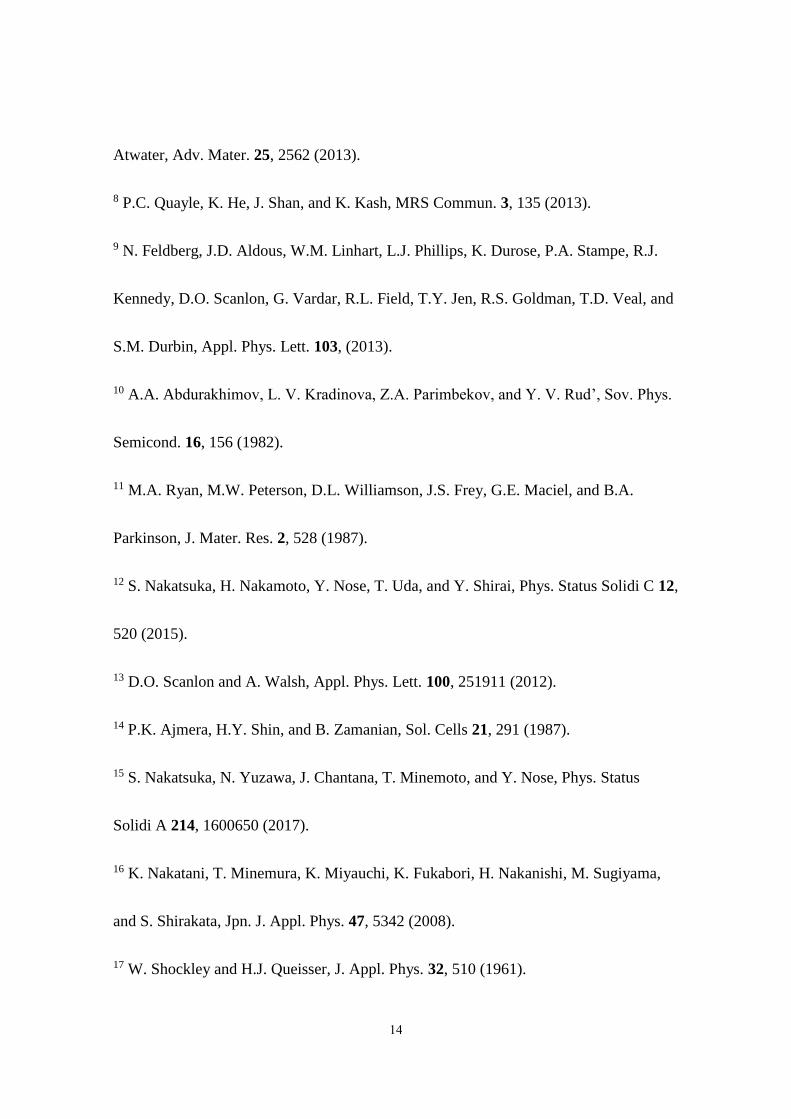
Figure 1 shows cross-sectional STEM images and corresponding elemental mappings
of the samples before and after phosphidation. Before phosphidation, it is observed that
the Cd-Sn precursor thin film was deposited on the ZnSnP2 bulk crystal with rough
morphology as shown in Figure 1 (a). From the contrast between Cd-L and Sn-L in the
elemental mappings, it can be recognized that Cd and Sn particles were separated,
particularly understandable around center area, which was also observed on the glass
substrates in our previous work24. It is consistent with that the phase diagram of the Cd-
Sn system is a typical eutectic diagram.25 Figure 1 (b) shows the formation of compounds
or alloys containing Cd, Sn and P on the ZnSnP2 bulk crystal by phosphidation. This
7
indicates the formation of CdSnP2/ZnSnP2 junction when considering together with
SAED pattern shown later. Comparing the STEM images before and after phosphidation,
it is observed that the original boundary between Cd-Sn precursor thin film and ZnSnP2
bulk crystal changed from flat to curved boundary. In addition, Zn was also detected in
the Cd-Sn-P region. On the other hand, the junction was inhomogeneously formed and
the precipitation of Sn was observed at the interface as shown in Figure 1 (c). Figures 1
(b) and 1 (c) are different areas in the same sample. The realization of homogeneous
interfacial structure is thus required as future works. The phosphidation is unsuitable for
smooth interface because of the roughness of Cd-Sn precursor films, and then deposition
methods such as molecular beam epitaxy (MBE) is desirable.
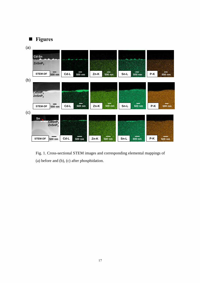
Then, TEM observation was carried out and SAED patterns were taken from each
region around the interface to investigate the crystal structure, as shown in Figure 2.
ZnSnP2 <110> was selected as the zone axis. The SAED patterns in ZnSnP2 and Cd-Sn-
P regions show the same pattern, indicating that the crystal structure in the Cd-Sn-P region
is same as ZnSnP2. In other words, CdSnP2 with chalcopyrite structure was grown on
ZnSnP2 by phosphidation. In addition, both phosphides show the same orientation and
thus the epitaxial relationship between CdSnP2 and ZnSnP2 is understood. From the
viewpoint of carrier transport in photovoltaic devices, such an epitaxial growth is

8
considered to be favourable to achieve a higher conversion efficiency. On the other hand,
the SAED pattern at the interface shown in Figure 2 (c) seems to be an overlap of those
taken from ZnSnP2 and CdSnP2 regions. To investigate the detailed structure at the
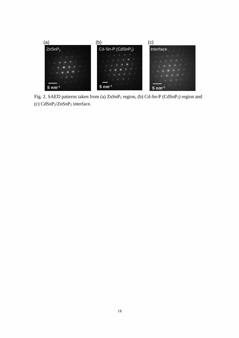
CdSnP2/ZnSnP2 interface, the composition analysis based on STEM-EDX was carried
out. Figure 3 shows the composition distribution across the interface of CdSnP2/ZnSnP2.
The composition was evaluated based on the Cliff-Lorimer method, where Sn was
selected as the base element and k-factor of Zn and P were calculated using the ZnSnP2
bulk crystal region, and that of Cd was obtained using the CdSnP2 bulk crystal sample
separately prepared. The compositions of P and Sn are approximately 50 and 25 at. %,
respectively, independent of the scanned positions except for the surface, and the
composition change of Zn and Cd is observed. This means that the formation of the solid
solutions between CdSnP2 and ZnSnP2, (Cd,Zn)SnP2, which is also supported by the
SAED pattern at the interface as shown in Figure 2 (c). The concentration change is
continuous and the interface with less lattice defects might be formed. In addition, in the
CdSnP2 region, the concentration of Zn is at least 5 at.%, which correspond to the mole
fraction [Zn]/([Cd]+[Zn]) of 0.2. On the other hand, Cd was hardly detected in the ZnSnP2
bulk crystal side. In this work, the heat treatment was not carried out after the formation
of CdSnP2 and the above asymmetric composition distribution is due to the Zn diffusion

9
into CdSnP2 region during phosphidation. From the above experimental results, the
obtained (Cd,Zn)SnP2/ZnSnP2 interface can be recognized as a homointerface due to both
compounds thermodynamically-indistinguishable although it is considered a
heterointerface at first sight. It is thus expected that the above diffusion behavior is
controlled by experimental conditions such as heat treatment during phosphidation and
preparation of precursor thin films, and it is a key to obtain favorable interface for
photovoltaic application.
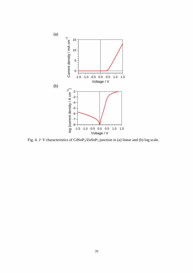
Finally, the J−V characteristics were measured using the sample with the structure of
Sn/CdSnP2/ZnSnP2/Cu. Figure 4 shows the J−V curves in linear and log scale. As shown
in these figures, a rectifying behavior is observed, suggesting the formation of a pn-
junction at the n-(Cd,Zn)SnP2/p-ZnSnP2 interface because Cu/ZnSnP2 and Sn/CdSnP2
junctions have been known to show an Ohmic behavior in our preliminary works. The
conventional J−V relationship for single-diode expressed by the equation (1) was fitted
to the measured curve,
s s
0
sh
( )exp 1
q V R J V R JJ J
NkT R
− − = − +
, (1)
where k is the Boltzmann constant and T is the temperature. Consequently, the diode
parameters such as saturation current density, J0, ideality factor, N, series resistance, RS,
10
and shunt resistance, RSh, were evaluated to be 1.41×10⁻⁸ A cm−2, 1.66, 68.9 Ω cm2 and
8.50×10⁵ Ω cm2, respectively. Comparing the parameters for CdS/CIGS junction26, the
series resistance and the saturation current density are relatively high for photovoltaic
application. One of the reasons is inhomogeneity of (Cd,Zn)SnP2/ZnSnP2 junction as
described in the STEM analysis and it should be established to prepare the uniform
junction over the entire interface. The high resistivity of CdSnP2 prepared by
phosphidation24, resulting in high series resistance in Figure 4, should be also considered.
The above improvement is required for the detailed analysis for interface such as
capacitance-voltage measurements and the device fabrication as future works.

11
4. Conclusions
In this study, Cd-Sn precursor thin films were prepared on ZnSnP2 bulk crystals grown
by flux method and then CdSnP2 thin films were formed by the phosphidation method for
fabrication of CdSnP2/ZnSnP2 junction. STEM-EDX analysis and SAED patterns
revealed that CdSnP2 with chalcopyrite structure was epitaxially grown on ZnSnP2 bulk
crystals. In addition, the diffusion of Zn into CdSnP2 region during phosphidation was
observed, while the concentrations of P and Sn are independent of positions around the
interface. The above results indicate that favourable junction was obtained due to the
formation of solid solution, (Cd,Zn)SnP2, in the view point of carrier transport. However,
n-(Cd,Zn)SnP2/p-ZnSnP2 junction was inhomogeneous and Sn was precipitated in some
areas around the interface, which should be improved in future works. In the J−V
characteristic of the junction, a rectifying behavior was observed although the series
resistance and the saturation current density were relatively high. It is thus concluded that
the n-(Cd,Zn)SnP2/p-ZnSnP2 junction obtained in this work can be recognized as a pn-
homojunction and this work is one of fundamentals to have more choices for solar
absorbing materials including II-IV-V2 type compounds.
12
Acknowledgements
The authors would like to express their gratitude to Dr. R. Katsube (Kyoto Univ.) for
his fruitful discussions. This work was financially supported by JST CREST Grant
Number JPMJCR17J2, The Mitsubishi Foundation and Grant-in-Aid for JSPS Research
Fellow Number 16J09443. This work was also supported by the Collaborative Research
Project of Laboratory for Materials and Structures, Institute of Innovative Research,
Tokyo Institute of Technology.
13
References
1 Solar Frontier. Solar Frontier Achieves World Record Thin-Film Solar Cell Efficiency
of 22.9%. http://www.solar-frontier.com/eng/news/2017/1220_press.html (accessed in
August 2018).
2 First Solar. First Solar Hits Record 22.1% Conversion Efficiency for CdTe Solar Cell.
https://www.greentechmedia.com/articles/read/First-Solar-Hits-Record-22.1-
Conversion-Efficiency-For-CdTe-Solar-Cell (accessed in August 2018).
3 J. Benick, R. Müller, F. Schindler, A. Richter, H. Hauser, F. Feldmann, P. Krenckel, S.
Riepe, M. C. Schubert, M. Hermle, S. W. Glunz, Approaching 22% Efficiency with
Multicrystalline N-Type Silicon Solar Cells, 33rd European PV Solar Energy Conference
and Exhibition, Amsterdam, Nertherlands 25−29 Sep (2017).
4 S. Akari, J. Chantana, S. Nakatsuka, Y. Nose, and T. Minemoto, Sol. Energy Mater. Sol.
Cells 174, 412 (2018).
5 S. Nakatsuka, S. Akari, J. Chantana, T. Minemoto, and Y. Nose, ACS Appl. Mater.
Interfaces 9, 33827 (2017).
6 N. Yuzawa, J. Chantana, S. Nakatsuka, Y. Nose, and T. Minemoto, Curr. Appl. Phys.
17, 557 (2017).
7 L. Lahourcade, N.C. Coronel, K.T. Delaney, S.K. Shukla, N.A. Spaldin, and H.A.
14
Atwater, Adv. Mater. 25, 2562 (2013).
8 P.C. Quayle, K. He, J. Shan, and K. Kash, MRS Commun. 3, 135 (2013).
9 N. Feldberg, J.D. Aldous, W.M. Linhart, L.J. Phillips, K. Durose, P.A. Stampe, R.J.
Kennedy, D.O. Scanlon, G. Vardar, R.L. Field, T.Y. Jen, R.S. Goldman, T.D. Veal, and
S.M. Durbin, Appl. Phys. Lett. 103, (2013).
10 A.A. Abdurakhimov, L. V. Kradinova, Z.A. Parimbekov, and Y. V. Rud’, Sov. Phys.
Semicond. 16, 156 (1982).
11 M.A. Ryan, M.W. Peterson, D.L. Williamson, J.S. Frey, G.E. Maciel, and B.A.
Parkinson, J. Mater. Res. 2, 528 (1987).
12 S. Nakatsuka, H. Nakamoto, Y. Nose, T. Uda, and Y. Shirai, Phys. Status Solidi C 12,
520 (2015).
13 D.O. Scanlon and A. Walsh, Appl. Phys. Lett. 100, 251911 (2012).
14 P.K. Ajmera, H.Y. Shin, and B. Zamanian, Sol. Cells 21, 291 (1987).
15 S. Nakatsuka, N. Yuzawa, J. Chantana, T. Minemoto, and Y. Nose, Phys. Status
Solidi A 214, 1600650 (2017).
16 K. Nakatani, T. Minemura, K. Miyauchi, K. Fukabori, H. Nakanishi, M. Sugiyama,
and S. Shirakata, Jpn. J. Appl. Phys. 47, 5342 (2008).
17 W. Shockley and H.J. Queisser, J. Appl. Phys. 32, 510 (1961).

15
18 T. Yokoyama, F. Oba, A. Seko, H. Hayashi, Y. Nose, and I. Tanaka, Appl. Phys.
Express 6, 61201 (2013).
19 H.Y. Shin and P.K. Ajmera, Mater. Lett. 5, 211 (1987).
20 Y. Kumagai, M. Choi, Y. Nose, and F. Oba, Phys. Rev. B 90, 125202 (2014).
21 S. Nakatsuka, Y. Nose, and Y. Shirai, J. Appl. Phys. 119, 193107 (2016).
22 J.L. Shay and J.H. Wernick, Chalcopyrite Semiconductors: Growth, Electronic
Properties, and Applications (Pergamon Press, Oxford, 1975).
23 Y. Hinuma, F. Oba, Y. Nose, and I. Tanaka, J. Appl. Phys. 114, 043718 (2013).
24 S. Nakatsuka, R. Inoue, and Y. Nose, ACS Appl. Energy Mater. 1, 1635 (2018).
25 H. Okamoto, Phase Diagram for Binary Alloys, Desk Handbook (ASM International,
2000)
26 P. Jackson, D. Hariskos, R. Wuerz, O. Kiowki, A. Bauer, T. M. Friedlmeier, and M.
Powalla, Phys. Status Solidi RRL, 9, 28 (2015).

16
◼ Figure captions
Figure 1. Cross-sectional STEM images and corresponding elemental mappings of (a)
before and (b), (c) after phosphidation.
Figure 2. SAED patterns taken from (a) ZnSnP2 region, (b) Cd-Sn-P (CdSnP2) region and
(c) CdSnP2/ZnSnP2 interface.
Figure 3. Composition analysis at CdSnP2/ZnSnP2 interface based on STEM-EDX.
Figure 4. J−V characteristics of CdSnP2/ZnSnP2 junction in (a) linear and (b) log scale.
17
◼ Figures
(a)
(b)
(c)
Fig. 1. Cross-sectional STEM images and corresponding elemental mappings of
(a) before and (b), (c) after phosphidation.
STEM-DF 500 nm
ZnSnP2
Cd-Sn
Cd-L 500 nm Zn-K 500 nm Sn-L 500 nm P-K 500 nm
STEM-DF
ZnSnP2
CdSnP2
Cd-L 500 nm500 nm Zn-K 500 nm Sn-L 500 nm P-K 500 nm
Cd-L 500 nm500 nmSTEM-DF
ZnSnP2
SnCdSnP2
Zn-K 500 nm Sn-L 500 nm P-K 500 nm
18
(a) (b) (c)
Fig. 2. SAED patterns taken from (a) ZnSnP2 region, (b) Cd-Sn-P (CdSnP2) region and
(c) CdSnP2/ZnSnP2 interface.
ZnSnP2
5 nm−1
Cd-Sn-P (CdSnP2)
5 nm−1
Interface
5 nm−1
19
Fig. 3. Composition analysis at CdSnP2/ZnSnP2 interface based on STEM-EDX.
60
50
40
30
20
10
0
Com
positio
n /
at.
%
400350300250200150100500
Distance / nm
Zn Cd Sn P
STEM-DF
ZnSnP2
CdSnP2
500 nm
Scan
direction
20
(a)
(b)
Fig. 4. J−V characteristics of CdSnP2/ZnSnP2 junction in (a) linear and (b) log scale.
15
10
5
0C
urr
ent
density / m
A c
m–2
-1.5 -1.0 -0.5 0.0 0.5 1.0 1.5
Voltage / V
-8
-7
-6
-5
-4
-3
-2
log (
curr
ent
density /
A c
m–2)
-1.5 -1.0 -0.5 0.0 0.5 1.0 1.5
Voltage / V