SEMICONDUCTORS - KHIT
19
Page 1 SEMICONDUCTORS Material which allows partial flow of electricity through it is called semiconductor .Conductivity of semiconductor lies between conductors and insulators. Silicon and Germanium are the examples for semiconductors. The energy gap for Si is 1.1eV and for Ge is 0.7eV. INTRINSIC or PURE SEMICONDUCTOR Let us consider ‘Si’ with atomic no. 14 and valence is 4. All the silicon atoms form covalent bonds with the neighboring Si atom and no electron is free for conduction at temperature 0 k. Hence pure silicon acts as insulator at absolute o k, as the temperature increases above 0 k, these covalent bonds break and some electrons are released. These electrons move in the crystal freely and responsible for conductivity. So they are called free electrons. Each electron leaves behind an empty space called a hole which also acts as current carrier. These electrons and holes move in opposite directions under the effect of external field and constitute current. ELECTRON CONCENTRATION IN THE CONDUCTION BAND OF INTRINSIC SEMICONDUCTOR The no. of electrons per unit volume having energy in a range E and E+dE in the conduction band of an intrinsic semiconductor is, dn = Z(E)dE F(E) ----------(1) where F(E) represents the Fermi distribution function gives the probability of occupation of electron with energy E. F(E) = T K E E B F exp 1 1 Z(E) is the density of states i.e. no. of available states per unit volume of semiconductor. Z(E) = 3 4 h (2m) 3/2 E 1/2 dn = 3 4 h (2m) 3/2 E 1/2 . T K E E B F exp 1 1 dE SEMICONDUCTORS APPLIED PHYSICS UNIT I V
-
Upload
khangminh22 -
Category
Documents
-
view
0 -
download
0
Transcript of SEMICONDUCTORS - KHIT
Page 1
SEMICONDUCTORS Material which allows partial flow of electricity through it is called semiconductor .Conductivity of semiconductor lies between conductors and insulators. Silicon and Germanium are the examples for semiconductors. The energy gap for Si is 1.1eV and for Ge
is 0.7eV.
INTRINSIC or PURE SEMICONDUCTOR Let us consider ‘Si’ with atomic no. 14 and valence is 4. All the
silicon atoms form covalent bonds with the neighboring Si atom
and no electron is free for conduction at temperature 0 k. Hence
pure silicon acts as insulator at absolute o k, as the temperature
increases above 0 k, these covalent bonds break and some
electrons are released. These electrons move in the crystal freely
and responsible for conductivity. So they are called free electrons.
Each electron leaves behind an empty space called
a hole which also acts as current carrier. These electrons and
holes move in opposite directions under the effect of external
field and constitute current.
ELECTRON CONCENTRATION IN THE CONDUCTION BAND OF INTRINSIC SEMICONDUCTOR The no. of electrons per unit volume having energy in a range E and E+dE in the conduction band of an intrinsic semiconductor is, dn = Z(E)dE F(E) ----------(1) where F(E) represents the Fermi distribution function gives the probability of occupation of electron with energy E.
F(E) =
TK
EE
B
Fexp1
1
Z(E) is the density of states i.e. no. of available states per unit volume of semiconductor.
Z(E) = 3
4
h
(2m)3/2 E1/2
dn = 3
4
h
(2m)3/2 E1/2 .
TK
EE
B
Fexp1
1dE
SEMICONDUCTORSAPPLIED PHYSICS
UNIT IV
SEMICONDUCTORS
Page 2
For conduction band,
dn = 3
4
h
(2m*
e)3/2 (E-Ec)1/2 .
TK
EE
B
Fexp1
1dE -------------- (2)
Where *em is effective mass of electron in the conduction band.
in the above equation, for conduction band,
TK
EE
B
Fexp >> 1 so 1 can be neglected in the denominator
of the equ.(2).
dn = 3
4
h
(2m*
e)3/2 (E-Ec)1/2
TK
EE
B
F )(exp -------------(3)
To get the total no. of electrons per unit vol. in the conduction band is we have to integrate the above equ.
Between the bottom of the conduction to top of the conduction band.
n = 3
4
h
(2m*
e)3/2
cE(E-Ec)1/2
TK
EE
B
F )(exp dE
dn = 3
4
h
(2m*
e)3/2
cE
(E-Ec)1/2
TK
EEEE
B
ccF )(exp dE
n = 3
4
h
(2m*
e)3/2
TK
EE
B
cF )(exp
cE(E-Ec)1/2
TK
EE
B
c )(exp dE
put x =
TK
EE
B
c )(, so that dE = KBTdx
Lower Limit: when E = Ec, x = 0 and
Upper Limit: when E = ∞, x = ∞
n = 3
4
h
(2m*
e)3/2
TK
EE
B
cF )(exp
0e-x (xKBT)1/2 KBT dx
n = 3
4
h
(2m*
ekBT)3/2
TK
EE
B
cF )(exp
0e-x (x)1/2 dx
n = 4Π 2
3
2
B*e
h
Tk2m
TK
EE
B
cF )(exp
2
APPLIED PHYSICS
Type your text
UNIT IV
SEMICONDUCTORS
Page 3
n = 22
3
2
B*e
h
Tkm 2
TK
EE
B
Fc )(exp
n = Nc
TK
EE
B
Fc )(exp
Where Nc = 22
3
2
B*e
h
Tkm 2
HOLE CONCENTRATION IN THE VALENCE BAND OF INTRINSIC SEMI CONDUCTOR The no. of holes per unit volume having energy in a range E and E+dE in the valence band of an intrinsic
semiconductor is,
dp = Z(E)dE [1-F(E)] ----------(1) where [1-F(E) ]represents the probability of absence of electron in the particular energy level with energy E.
[1-F(E)] = 1-
TK
EE
B
Fexp1
1 =
TK
EE
TK
EE
B
F
B
F
exp1
exp
For the valance band 1>>
TK
EE
B
Fexp .
So exponential term can be neglected in the denominator of the above equation.
[1-F(E)] =
TK
EE
B
Fexp
dP = 3
4
h
(2m)3/2 E1/2
TK
EE
B
Fexp dE
For valance band,
dp = 3
4
h
(2m*
h)3/2 (Ev-E)1/2
TK
EE
B
Fexp dE
To get the total no. of holes in the V.B. we have to integrate the above equation between the limits bottom
of the V.B. to top of the V.B.
p = 3
4
h
(2m*
h)3/2
vE
(Ev-E)1/2
TK
EE
B
Fexp dE
APPLIED PHYSICS
UNIT IV
SEMICONDUCTORS
Page 4
p = 3
4
h
(2m*
h)3/2
vE
(Ev-E)1/2
TK
EEEE
B
VVFexp dE
p = 3
4
h
(2m*
h)3/2
TK
EE
B
FVexp
vE
(Ev-E)1/2
TK
EE
B
Vexp dE
put
TK
EE
B
V = x ; dE = -dx KBT
Lower Limit: when E = -∞, x = ∞. Upper Limit: when E = Ev , x = 0.
p = 3
4
h
(2m*
h)3/2
TK
EE
B
FVexp
0
e-x (xKBT)1/2 (-KBT dx)
p = 3
4
h
( *
hm KBT)3/2
TK
EE
B
FVexp
0e-x x1/2 dx
p = 3
4
h
(2 *
hm KBT)3/2
TK
EE
B
FVexp 2
p = 22
3
2
*2
h
Tkm Bh
TK
EE
B
FVexp or
p = Nv
TK
EE
B
VFexp ----------- (2)
Where Nv = 22
3
2
*2
h
Tkm Bh
Equ. (2) gives the no. of holes in the V.B of the intrinsic semi conductor. LOCATION OF FERMI LEVEL IN INTRINSIC SEMICONDUCTOR In intrinsic semiconductor no. of electrons in the C.B and no. of holes in the V.B are equal.
n = p
Nc
TK
EE
B
Fc )(exp = Nv
TK
EE
B
VFexp
APPLIED PHYSICS
UNIT IV
SEMICONDUCTORS
Page 5
TK
EEEE
B
vFFcexp = CN
Nv
TK
E
B
F2-
TK
EE
B
VC )( = ln
CN
Nv
EF = 2
Ev)(Ec+
2
TK B ln CN
Nv ----------- (1)
At T = 0 k,
EF = 2
Ev)(Ec-------- (2)
Fermi energy level lies exactly in the middle of the forbidden gap at absolute zero K. INTRINSIC CARRIER CONCENTRATION (ni) [law of mass action] In the intrinsic semiconductor, n = p = ni .Where ni is known as intrinsic carrier concentration.
np = 2in
2in = 2
23
2
B*e
h
Tkm 2
TK
EE
B
Fc )(exp 2
2
*2
h
Tkm Bh
TK
EE
B
VFexp
2in = 4
3
2
B
h
Tk 2
23
**he mm
TK
EEEE
B
VFFc )exp
2in = 4
3
2
B
h
Tk 2
23
**he mm
TK
EE
B
Vc )(exp
ni = 2
23
2
B
h
Tk 2
43
**he mm
TK
E
B
g
2
)exp (since Ec-Ev = Eg)
This equ Shows that for a given semiconductor the product of holes and electron concentration at a given
temp. is equal to square of the intrinsic semiconductor carrier concentration. This is called law of mass
action and holds both for intrinsic and extrinsic semiconductors.
CONDUCTIVITY OF INTRINSIC SEMICONDUCTORS When the electric field is applied to the semiconductor, charge carriers acquire velocity. vd α E vd = µE --------- (1) where µ is called mobility of charge carriers.
APPLIED PHYSICS
UNIT IV
SEMICONDUCTORS
Page 6
Current density J = ne vd
J = neµE ---------- (2)
This is in the form of J = E
Where = neµ --------- (3) is conductivity
For electrons n = neµe
For holes p = peµh
Where µe ,µh are mobilities of electrons and holes respectively. = neµe + peµh
= (nµe + pµh )e = ni(µe + µh)e --------- (4) where ni is called intrinsic carrier concentration.
= 2
23
2
B
h
Tk 2
43
**he mm
TK
E
B
g
2
)exp (µe + µh)e
= o
TK
E
B
g
2
)exp where o =2
23
2
B
h
Tk 2
43
**he mm (µe + µh)e
ln = ln o - TK
E
B
g
2-----------(4)
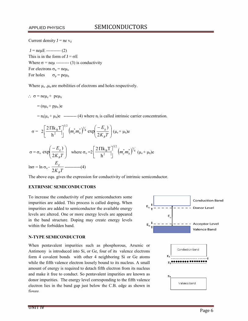
The above equ. gives the expression for conductivity of intrinsic semiconductor. EXTRINSIC SEMICONDUCTORS
N-TYPE SEMICONDUCTOR
To increase the conductivity of pure semiconductors some
impurities are added. This process is called doping. When
impurities are added to semiconductor the available energy
levels are altered. One or more energy levels are appeared
in the band structure. Doping may create energy levels
within the forbidden band.
When pentavalent impurities such as phosphorous, Arsenic or
Antimony is introduced into Si, or Ge, four of its valence electrons
form 4 covalent bonds with other 4 neighboring Si or Ge atoms
while the fifth valence electron loosely bound to its nucleus. A small
amount of energy is required to detach fifth electron from its nucleus
and make it free to conduct. So pentavalent impurities are known as
donor impurities. The energy level corresponding to the fifth valence
electron lies in the band gap just below the C.B. edge as shown in
figure.
APPLIED PHYSICS
UNIT IV
SEMICONDUCTORS
Page 7
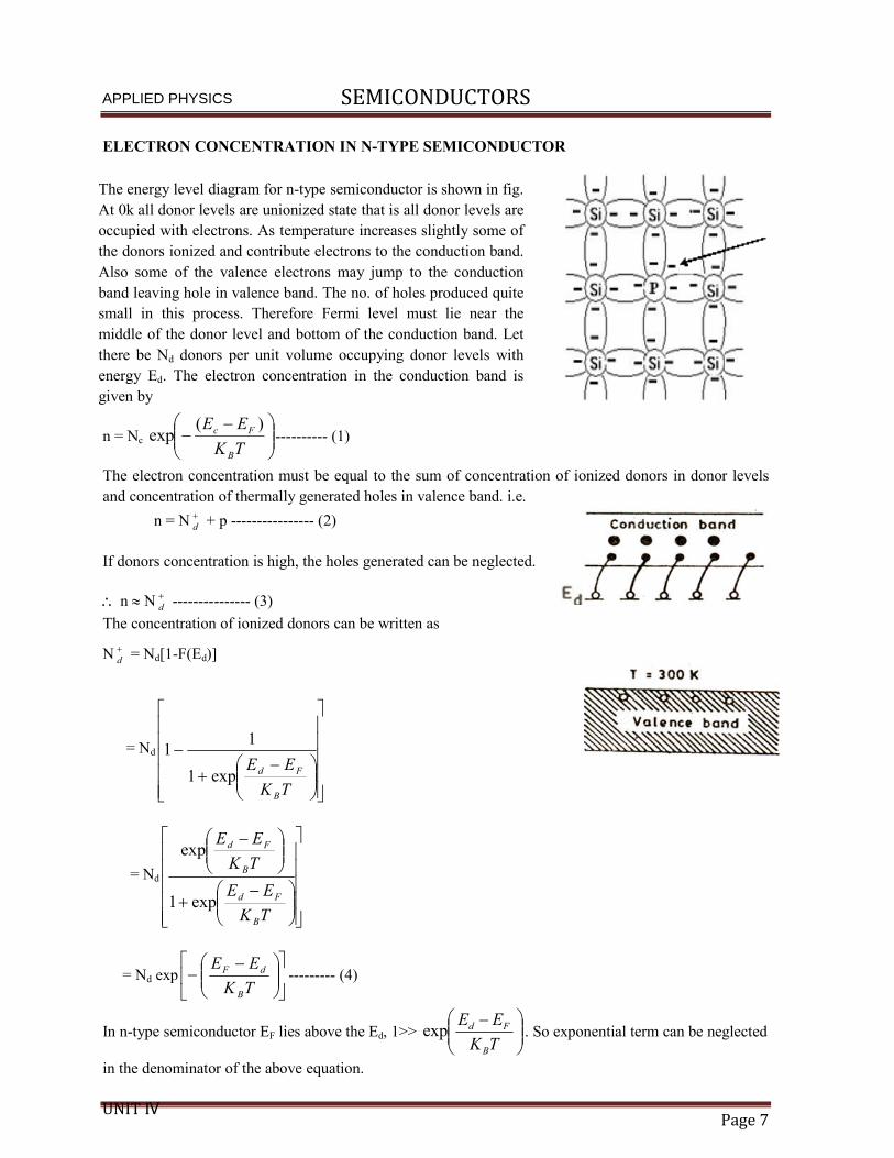
ELECTRON CONCENTRATION IN N-TYPE SEMICONDUCTOR
n = Nc
TK
EE
B
Fc )(exp ---------- (1)
The electron concentration must be equal to the sum of concentration of ionized donors in donor levels
and concentration of thermally generated holes in valence band. i.e.
n = N d + p ---------------- (2)
If donors concentration is high, the holes generated can be neglected.
n N d --------------- (3)
The concentration of ionized donors can be written as
N d = Nd[1-F(Ed)]
= Nd
TK
EE
B
Fdexp1
11
= Nd
TK
EE
TK
EE
B
Fd
B
Fd
exp1
exp
= Nd exp
TK
EE
B
dF --------- (4)
In n-type semiconductor EF lies above the Ed, 1>>
TK
EE
B
Fdexp . So exponential term can be neglected
in the denominator of the above equation.
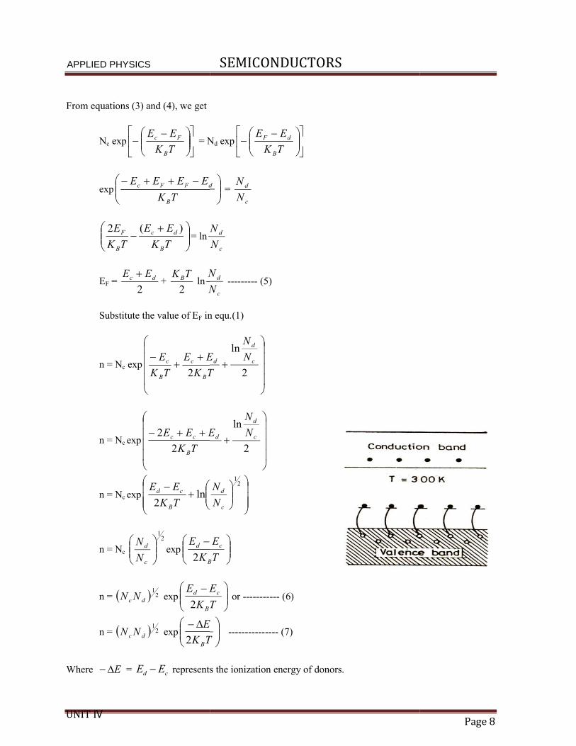
The energy level diagram for n-type semiconductor is shown in fig.
At 0k all donor levels are unionized state that is all donor levels are
occupied with electrons. As temperature increases slightly some of
the donors ionized and contribute electrons to the conduction band.
Also some of the valence electrons may jump to the conduction
band leaving hole in valence band. The no. of holes produced quite
small in this process. Therefore Fermi level must lie near the
middle of the donor level and bottom of the conduction band. Let
there be Nd donors per unit volume occupying donor levels with
energy Ed. The electron concentration in the conduction band is
given by
APPLIED PHYSICS
UNIT IV
From equations (3) and (4), we get
Nc exp
TK
EE
B
Fc = N
exp
TK
EEEE
B
dFFc
TK
EE
TK
E
B
dc
B
F )(2= ln
N
EF = 2
dc EE +
2
TK B lnN
N
Substitute the value of EF in equ.(1)
n = Nc exp
2 B
c
B
c
TK
EE
TK
E
n = Nc exp
2
2
B
cc
TK
EEE
n = Nc exp
ln
2 B
cd
TK
EE
n = Nc 2
1
c
d
N
Nexp
K
E
B
d
2
n = 21
dc NN exp
TK
EE
B
d
2
n = 21
dc NN exp
TK
E
B2
Where E = cd EE represents the ionization energy of donors.
SEMICONDUCTORS
= Nd exp
TK
EE
B
dF
d =
c
d
N
N
c
d
N
N
c
d
N
N --------- (5)
in equ.(1)
2
lnc
d
d N
N
T
E
2
lnc
d
d N
N
E
21
c
d
N
N
T
E
B
c
T
Ec or ----------- (6)
T
E --------------- (7)
represents the ionization energy of donors.
Page 8
APPLIED PHYSICS
UNIT IV
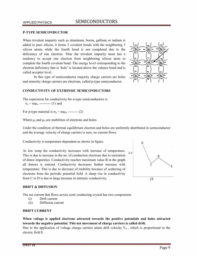
P-TYPE SEMICONDUCTOR
When trivalent impurity such as aluminum, boron, gallium or indium is
added to pure silicon, it forms 3 covalent bonds with the neighboring 3
silicon atoms while the fourth bond is not completed due to the
deficiency of one electron. Thus the trivalent impurity atom has a
tendency to accept one electron from neighboring silicon atom
complete the fourth covalent bond. The energy level corresponding to the
electron deficiency that is ‘hole’ is located above the valence bond and is
called acceptor level.
In this type of semiconductor majority charge carriers are holes
and minority charge carriers are electrons, called p
CONDUCTIVITY OF EXTRINSIC SEMICONDUCTORS
The expression for conductivity for n e = nee ---------- (1) and For p-type material is p = neh --------- Where e and h are mobilities of electrons and holes. Under the condition of thermal equilibrium electron and holes are uniformly distributed in semiconductor
and the average velocity of charge carrie
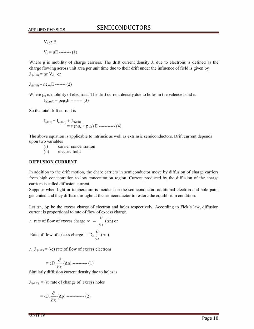
Conductivity is temperature dependent
At low temp the conductivity increases
This is due to increase in the no. of conduction
of donor impurities. Conductivity reaches maximum
all donors is ionized. Conductivity decreases further increase
temperature. This is due to decrease of mobility because of scattering of
electrons from the periodic potential field. A sharp rise in conductivity
from C to D is due to large increase in intrinsic conductivity.
DRIFT & DIFFUSION The net current that flows across semi conducting
(i) Drift current (ii) Diffusion current
DRIFT CURRENT When voltage is applied electrons attracted towards the positive potentials and holes attracted
towards the negative potential. This net movement of charge carriers is called drift.
Due to the application of voltage charge carriers attain dr
electric field E.
SEMICONDUCTORS
such as aluminum, boron, gallium or indium is
added to pure silicon, it forms 3 covalent bonds with the neighboring 3
silicon atoms while the fourth bond is not completed due to the
deficiency of one electron. Thus the trivalent impurity atom has a
cy to accept one electron from neighboring silicon atom to
complete the fourth covalent bond. The energy level corresponding to the
is located above the valence bond and is
semiconductor majority charge carriers are holes
and minority charge carriers are electrons, called p-type semiconductor.
CONDUCTIVITY OF EXTRINSIC SEMICONDUCTORS
The expression for conductivity for n-type semiconductors is
--------- (2)
are mobilities of electrons and holes.
Under the condition of thermal equilibrium electron and holes are uniformly distributed in semiconductor
of charge carriers is zero, no current flows.
temperature dependent as shown in figure.
conductivity increases with increase of temperature.
of conduction electrons due to ionization
of donor impurities. Conductivity reaches maximum value B in the graph
Conductivity decreases further increase with
temperature. This is due to decrease of mobility because of scattering of
the periodic potential field. A sharp rise in conductivity
from C to D is due to large increase in intrinsic conductivity.
semi conducting crystal has two components.
When voltage is applied electrons attracted towards the positive potentials and holes attracted
towards the negative potential. This net movement of charge carriers is called drift.
Due to the application of voltage charge carriers attain drift velocity Vd , which is proportional to the
Page 9
Under the condition of thermal equilibrium electron and holes are uniformly distributed in semiconductor
When voltage is applied electrons attracted towards the positive potentials and holes attracted
towards the negative potential. This net movement of charge carriers is called drift.
, which is proportional to the
APPLIED PHYSICS
UNIT IV
SEMICONDUCTORS
Page 10
Vd E Vd = µE -------- (1)
Where µ is mobility of charge carriers. The drift current density Je due to electrons is defined as the
charge flowing across unit area per unit time due to their drift under the influence of field is given by
Je(drift) = ne Vd or Je(drift) = neµeE ------- (2) Where µe is mobility of electrons. The drift current density due to holes in the valence band is
Jh(druft) = peµhE -------- (3) So the total drift current is J(drift) = Je(drift) + Jh(drift)
= e (nµe + pµh) E ----------- (4) The above equation is applicable to intrinsic as well as extrinsic semiconductors. Drift current depends upon two variables
(i) carrier concentration (ii) electric field
DIFFUSION CURRENT In addition to the drift motion, the chare carriers in semiconductor move by diffusion of charge carriers
from high concentration to low concentration region. Current produced by the diffusion of the charge
carriers is called diffusion current.
Suppose when light or temperature is incident on the semiconductor, additional electron and hole pairs
generated and they diffuse throughout the semiconductor to restore the equilibrium condition.
Let n, p be the excess charge of electron and holes respectively. According to Fick’s law, diffusion current is proportional to rate of flow of excess charge.
rate of flow of excess charge x
(n) or
Rate of flow of excess charge = -Dex
(n)
Je(diff.) = (-e) rate of flow of excess electrons
= eDex
(n) ---------- (1)
Similarly diffusion current density due to holes is Jh(diff.) = (e) rate of change of excess holes
= -Dhx
(p) ------------ (2)
APPLIED PHYSICS
UNIT IV
SEMICONDUCTORS
Page 11
Total current density in semiconductor due to electrons is Je = Je(drift) + Je(diff.)
= neµeE + eDex
(n)
= (nµeE + Dex
(n)) e ---------- (3)
Current density due to holes is Jh = Jh(drift) + Jh(diff.)
= peµhE + (-Dhx
(p))
Jh = (pµhE - Dhx
(p)) e ---------- (4)
EINSTEIN’S RELATION Einstein’s relation gives the direct relation between diffusion coefficient and mobility of charge carriers. At equilibrium condition drift current balances and opposite to the diffusion current .
neµeE = - eDex
n ---------- (1)
neµeE = -(1/µe) eDex
n ---------- (2)
Einstein compared the movement of charge carriers with the gas molecules in a container.
According to Boltzmann’s statistics the concentrations of gas molecules can be written as
n = C.exp
TK
Fx
B
where x is distance and F = eE is force acting on the charge carriers
x
n= C.exp
TK
eEx
B
.
TK
eE
B
, x
n= n.
TK
eE
B
----------- (3)
F=neE= TKBx
n ----------- (4)
neµeE = neDe
TK
eE
B
e
eD
=
e
TK B ---------- (2) for electrons h
hD
=
e
TK B --------- (3) for holes
APPLIED PHYSICS
UNIT IV
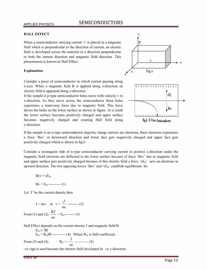
HALL EFFECT When a semiconductor carrying current ‘i’ is placed in a magnetic
field which is perpendicular to the direction of current, an electric
field is developed across the material in a direction perpendicular
to both the current direction and magnetic field direction. This
phenomenon is known as Hall Effect.
Explanation
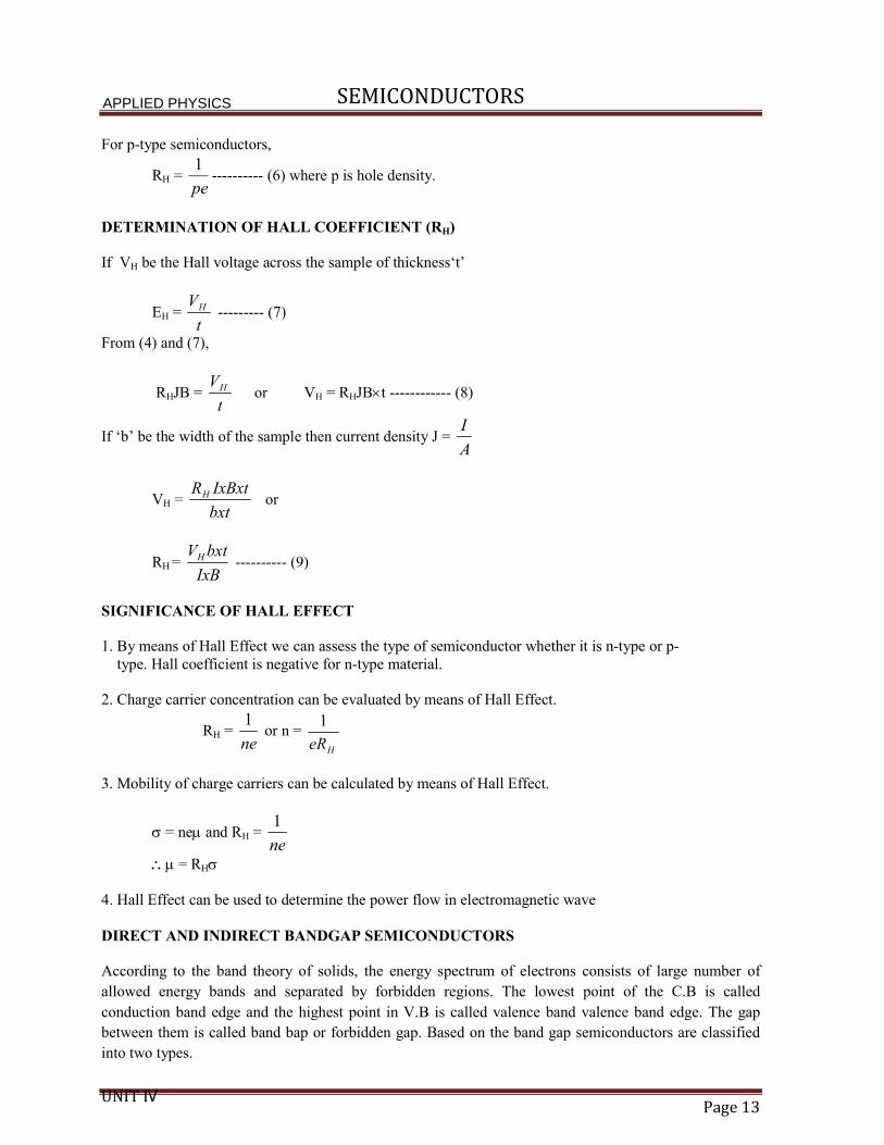
If the sample is an n-type semiconductor majority charge carriers are electrons, these electrons experience
a force ‘Bev’ in downward direction and lower face gets negatively charged and upp
positively charged which is shown in
Consider a rectangular slab of n-type semiconductor carrying current in positive x
magnetic field electrons are deflected
and upper surface gets positively charged because of this el
upward direction. The two opposing forces ‘Bev’ and
Bev = eEH Bv = EH ---------- (1) Let ‘J’ be the current density then
J = nev or v = ne
J ---------
From (1) and (2), ne
BJ = EH --------
Hall Effect depends on the current density J and magnetic field B. EH JB EH = RHJB ----------- (4) Where R
From (3) and (4), RH = -ne
1 -----------
-ve sign is used because the electric field developed
Consider a piece of semiconductor in which current passing along
x-axis. When a magnetic field B is applied along z
electric field is appeared along y-direction.
If the sample is p-type semiconductor holes move with velocity v in
x-direction. As they move across the semiconductor these holes
experience a transverse force due to magneti
drives the holes on the lower surface as shown in figure. As a result
the lower surface becomes positively charged and upper surface
becomes negatively charged and creating Hall field along
y-direction.
SEMICONDUCTORS
When a semiconductor carrying current ‘i’ is placed in a magnetic
field which is perpendicular to the direction of current, an electric
material in a direction perpendicular
to both the current direction and magnetic field direction. This
phenomenon is known as Hall Effect.
type semiconductor majority charge carriers are electrons, these electrons experience
a force ‘Bev’ in downward direction and lower face gets negatively charged and upp
positively charged which is shown in fig.b
type semiconductor carrying current in positive x-direction under the
deflected to the lower surface because of force ‘Bev’ due to magnetic field
and upper surface gets positively charged because of this electric field a force ‘eEH’ acts on electrons in
upward direction. The two opposing forces ‘Bev’ and ‘eEH’ establish equilibrium. So
--------- (2)
(3)
depends on the current density J and magnetic field B.
Where RH is Hall coefficient.
----------- (5)
ve sign is used because the electric field developed in –ve y-direction.
Consider a piece of semiconductor in which current passing along
B is applied along z-direction an
direction.
type semiconductor holes move with velocity v in
direction. As they move across the semiconductor these holes
experience a transverse force due to magnetic field. This force
drives the holes on the lower surface as shown in figure. As a result
the lower surface becomes positively charged and upper surface
becomes negatively charged and creating Hall field along
Page 12
type semiconductor majority charge carriers are electrons, these electrons experience
a force ‘Bev’ in downward direction and lower face gets negatively charged and upper face gets
direction under the
to the lower surface because of force ‘Bev’ due to magnetic field
acts on electrons in
APPLIED PHYSICS
UNIT IV
SEMICONDUCTORS
Page 13
For p-type semiconductors,
RH = pe
1---------- (6) where p is hole density.
DETERMINATION OF HALL COEFFICIENT (RH) If VH be the Hall voltage across the sample of thickness‘t’
EH = t
VH --------- (7)
From (4) and (7),
RHJB = t
VH or VH = RHJBt ------------ (8)
If ‘b’ be the width of the sample then current density J = A
I
VH = bxt
IxBxtRH or
RH = IxB
bxtVH ---------- (9)
SIGNIFICANCE OF HALL EFFECT 1. By means of Hall Effect we can assess the type of semiconductor whether it is n-type or p- type. Hall coefficient is negative for n-type material.
2. Charge carrier concentration can be evaluated by means of Hall Effect.
RH = ne
1 or n =
HeR
1
3. Mobility of charge carriers can be calculated by means of Hall Effect.
= ne and RH = ne
1
= RH 4. Hall Effect can be used to determine the power flow in electromagnetic wave DIRECT AND INDIRECT BANDGAP SEMICONDUCTORS According to the band theory of solids, the energy spectrum of electrons consists of large number of
allowed energy bands and separated by forbidden regions. The lowest point of the C.B is called
conduction band edge and the highest point in V.B is called valence band valence band edge. The gap
between them is called band bap or forbidden gap. Based on the band gap semiconductors are classified
into two types.
APPLIED PHYSICS
UNIT IV
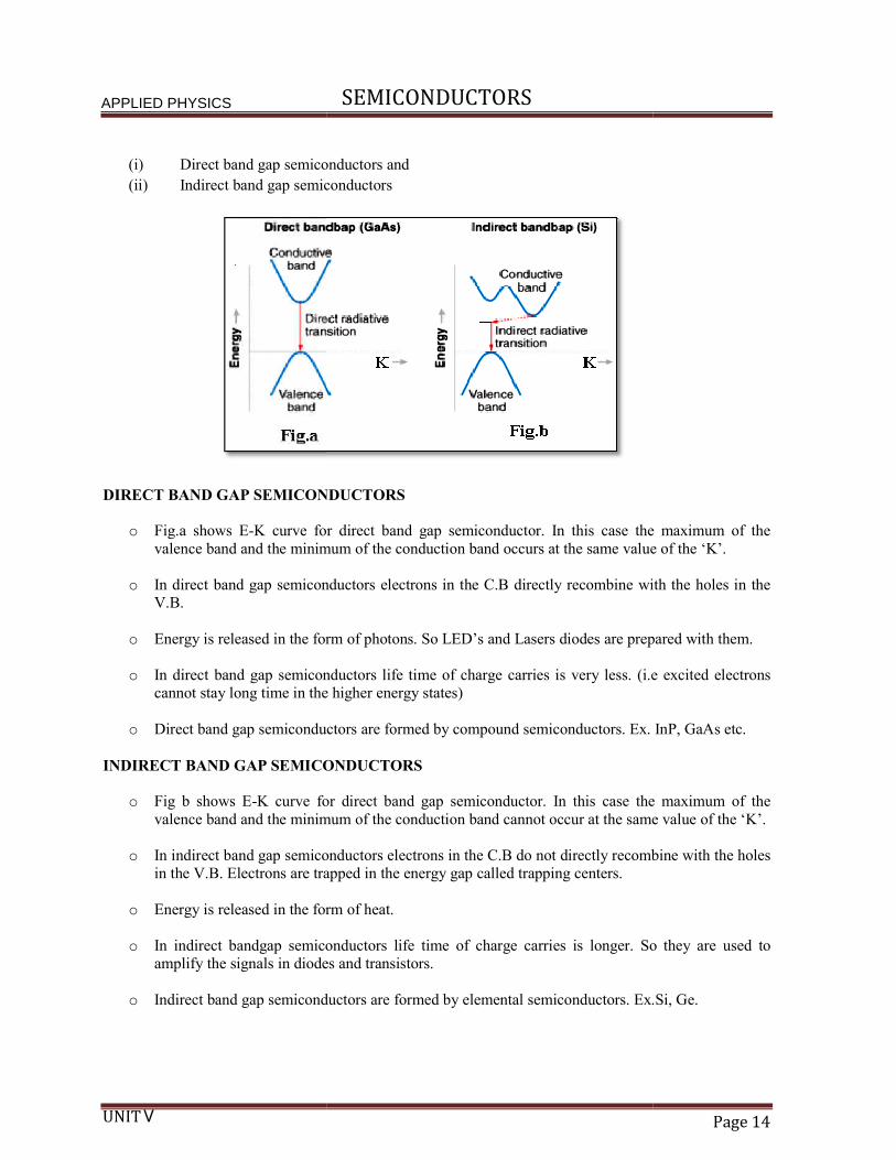
(i) Direct band gap semiconductors and
(ii) Indirect band gap semiconductors
DIRECT BAND GAP SEMICONDUCTORS
o Fig.a shows E-K curve for direct band gap semiconductor. In this case the maximum of the valence band and the minimum of the conduction band occurs at the same value of the
o In direct band gap semiconductors electrons in the C.B directly recombine wit
V.B.
o Energy is released in the form of photons
o In direct band gap semiconductors life time of charge carries is very less. (i.e excited ecannot stay long time in the higher energy states)
o Direct band gap semiconductors are formed by compound semiconductors. Ex. InP, GaAs etc.
INDIRECT BAND GAP SEMICONDUCTORS
o Fig b shows E-K curve for direct band gap semiconductor. In this case the valence band and the minimum of the conduction band cannot occur at the same value of the ‘K’.
o In indirect band gap semiconductors electrons in the C.B do not directly recombine with the holes
in the V.B. Electrons are trapped in the energy
o Energy is released in the form of
o In indirect bandgap semiconductors life time of charge carries is amplify the signals in diodes and transistors.
o Indirect band gap semiconductors are formed by
SEMICONDUCTORS
Direct band gap semiconductors and
Indirect band gap semiconductors
DIRECT BAND GAP SEMICONDUCTORS
K curve for direct band gap semiconductor. In this case the maximum of the valence band and the minimum of the conduction band occurs at the same value of the
In direct band gap semiconductors electrons in the C.B directly recombine wit
Energy is released in the form of photons. So LED’s and Lasers diodes are prepared with them.
In direct band gap semiconductors life time of charge carries is very less. (i.e excited ecannot stay long time in the higher energy states)
Direct band gap semiconductors are formed by compound semiconductors. Ex. InP, GaAs etc.
INDIRECT BAND GAP SEMICONDUCTORS
K curve for direct band gap semiconductor. In this case the valence band and the minimum of the conduction band cannot occur at the same value of the ‘K’.
In indirect band gap semiconductors electrons in the C.B do not directly recombine with the holes Electrons are trapped in the energy gap called trapping centers.
Energy is released in the form of heat.
direct bandgap semiconductors life time of charge carries is longer. So they are used to amplify the signals in diodes and transistors.
irect band gap semiconductors are formed by elemental semiconductors. Ex.
Page 14
K curve for direct band gap semiconductor. In this case the maximum of the valence band and the minimum of the conduction band occurs at the same value of the ‘K’.
In direct band gap semiconductors electrons in the C.B directly recombine with the holes in the
. So LED’s and Lasers diodes are prepared with them.
In direct band gap semiconductors life time of charge carries is very less. (i.e excited electrons
Direct band gap semiconductors are formed by compound semiconductors. Ex. InP, GaAs etc.
K curve for direct band gap semiconductor. In this case the maximum of the valence band and the minimum of the conduction band cannot occur at the same value of the ‘K’.
In indirect band gap semiconductors electrons in the C.B do not directly recombine with the holes
So they are used to
semiconductors. Ex.Si, Ge.
UNIT V
APPLIED PHYSICS
SEMICONDUCTORS
Page 15
SHORT ANSWER QUESTIONS
1. Define semiconductor
2. State and explain Bloch’s theorem
3. Differences between direct and indirect band gap semi conductors
4. Differences between Intrinsic and Extrinsic semi conductors
5. Write few applications of semiconductor
6. Write few applications of Hall Effect.
7. Define drift and diffusion currents
8. Explain electrical conductivity and resistivity in Intrinsic semiconductors with variation of
temperature.
9. Explain electrical conductivity and resistivity in P Type semiconductors with variation of
temperature
10. Explain electrical conductivity and resistivity in N Type semiconductors with variation of
temperature
11. Derive the expression for Fermi level in Intrinsic semiconductors and explain its variation with
temperature.
12. Derive the expression for Fermi level in P Type semiconductors and explain its variation with
temperature.
13. Derive the expression for Fermi level in N type semiconductors and explain its variation with
temperature.
14. Derive the expression for electric conductivity in Intrinsic semiconductors.
15. Indicate an energy level diagrams the conduction and valence bands, donor and acceptor levels for
intrinsic semiconductor.
LONG ANSWER QUESTIONS
16. Explain the classification of crystalline solids based on band theory
Or
Explain origin of energy bands in solids and based on energy bands. Distinguish conductor,
semiconductor and insulator.
17. Derive the expression for carrier concentration in intrinsic semi conductors
18. Derive the expression for intrinsic carrier concentration and Fermi energy in intrinsic semi
conductors
19. Derive the expression for electron concentration in n-type Extrinsic semiconductors.
20. Derive the expression for hole concentration in p-type Extrinsic semiconductors
21. Show that Fermi level is nearer to conduction band in a N-type semiconductor and discuss the
variation of conductivity with temperature of an n-type semiconductor.
22. Explain the concept of drift and diffusion currents and hence derive the relation between diffusion
and mobility
Or
Explain the concept of drift and diffusion currents and hence derive the Einstein’s equation.
23. Explain Hall Effect in semiconductors and derive the expression for Hall coefficient. Write the
applications of Hall effect
Or
State and explain Hall Effect in detail?
APPLIED PHYSICS
UNIT IV
SEMICONDUCTORS
Page 16
NUMERICALS
1. The RH of a specimen is 3.66×10⁻⁴ m-3c- 1.Its resistivity is 8.93×10⁻³ Ωm. Find µ and n.
2. The following data are given for intrinsic germanium at 300k ni = 2.4×10¹⁹/m3, µe=0.39 m2
V-1 s-1, µp=0.19 m2 V-1 s-1.Calculate the resistivity of sample.
3. The hall coefficient of a specimen is 3.66×10⁻⁴ m3C-1. Its resistivity is 8.93×10⁻³ Ω-m. Find
carrier density and mobility of charge carriers.
4. Find the Diffusion coefficient of an electron in silicon at 300 K, if µe is 0.19 m2/V-s
5. The resistivity of an intrinsic semiconductor is 4.5 ohm-m at 20⁰C and 2 ohm-m at 32⁰C
What is the energy gap.
MULTIPLE CHOICE QUESTIONS
1. Solids with high value of conductivity are called: a. Conductors b. Non – metal c. Insulator d. Semi conductor
2. Flow of electrons is affected by the following
a. Thermal vibrations b. Impurity atoms c. Crystal defects d. All
3. The unit of electrical conductivity is a. ohm / metre b. ohm / sq. M c. ohm / metre d. ohm / sq. m
4. All good conductors have high
a. resistance b. electrical conductivity c. electrical and thermal conductivity d. conductance
5. The probability that an electron in a metal occupies the Fermi-level, at any temperature
(>0 K) is: a. 0 b. 1 c. 0.5 d. None of these
6. For metals conduction band and valenceband are a. Fully occupied b. Empty c. Partially occupied d. Overlapping
7. What is the correct statement for an insulator? a. The band gap energy is very high b. The conduction band and valence cannot overlap c. The conduction band and valence band may overlap d. The conduction band and valence cannot have very little difference of energy
8. P-type and N-type extrinsic semiconductors are formed by adding impurities of valency?
a. 5 and 3 respectively. b. 5 and 4 respectively. c. 3 and 5 respectively. d. 3 and 4 respectively
9. The bond that exists in a semiconductor is
a. Ionic bond b. Covalent bond c. Metallic bond d. Hydrogen bond
10. A semiconductor is formed by ……… bonds. a. Covalent b. Electrovalent c. Co-ordinate d. None of the above
11. A semiconductor has ………… temperature coefficient of resistance.
a. Positive b. Zero c. Negative d. None of the above
UNIT IV
SEMICONDUCTORS
Page 17
12. The most commonly used semiconductor is ……….. a. Germanium b. Silicon c. Carbon d. Sulphur
13. 91. A semiconductor has generally……………… valence electrons.
a. 2 b. 3 c. 6 d. 4
14. The resistivity of pure germanium under standard conditions is about ………. a. 6 x 10⁴ Ω cm b. 60 Ω cm c. 3 x 10⁶ Ω cm d. 6 x 10⁻⁴ Ω cm
15. The resistivity of a pure silicon is about ……………
a. 100 Ω cm b. 6000 Ω cm c. 3 x 10⁵ Ω m d. 6 x 10⁻⁸ Ω cm
16. When a pure semiconductor is heated, its resistance ………….. a. Goes up b. Goes down c. Remains the same d. Can’t say
17. The strength of a semiconductor crystal comes from ……..
a. Forces between nuclei b. Forces between protons c. Electron-pair bonds d. None of the above
18. When a pentavalent impurity is added to a pure semiconductor, it becomes ………
a. An insulator b. An intrinsic semiconductor c. p-type semiconductor d. n-type
19. Addition of pentavalent impurity to a semiconductor creates many ……..
a. Free electrons b. Holes c. Valence electrons d. Bound electrons
20. A pentavalent impurity has ………. Valence electrons a. 3 b. 5 c. 4 d. 6
21. An n-type semiconductor is ………
a. Positively charged b. Negatively charged c. Electrically neutral d. None of the above
22. A trivalent impurity has ….. valence electrons
a. 4 b. 5 c. 6 d. 3
23. Addition of trivalent impurity to a semiconductor creates many …….. a. Holes b. Free electrons c. Valence electrons d. Bound electrons
24. A hole in a semiconductor is defined as …………….
a. A free electron b. The incomplete part of an electron pair bond c. A free proton d. A free neutron
25. The impurity level in an extrinsic semiconductor is about ….. of pure semiconductor. a. 10 atoms for 108 atoms b. 1 atom for 108 atoms c. 1 atom for 104 atoms d. 1 atom for 100 atoms
26. As the doping to a pure semiconductor increases, the bulk resistance of the semiconductor ..
a. Remains the same b. Increases c. Decreases d. None of the above
27. A hole and electron in close proximity would tend to ………. a. Repel each other b. Attract each other c. Have no effect on each other d. None of the above
UNIT IV
SEMICONDUCTORS
Page 18
28. In a semiconductor, current conduction is due to ……..
a. Only holes b. Only free electrons c. Holes and free electrons d. None of the above
29. The random motion of holes and free electrons due to thermal agitation is called ……….
a. Diffusion b. Pressure c. Ionisation d. None of the above
30. In an intrinsic semiconductor, the number of free electrons ……… a. Equals the number of holes b. Is greater than the number of holes c. Is less than the number of holes d. None of the above
31. At room temperature, an intrinsic semiconductor has ……….
a. Many holes only b. A few free electrons and holes c. Many free electrons only d. No holes or free electrons
32. At absolute temperature, an intrinsic semiconductor has ……….
a. A few free electrons b. Many holes c. Many free electrons d.No holes or free electrons
33. Pure semiconductors which conduct electricity on heating are called ________
semiconductors a. n-type b. Extrinsic c. Intrinsic d. p-type
34. Number of free electrons in conduction band is equal to number of holes in valence band in
_______ semiconductor a. n-type b. Extrinsic c. Intrinsic d. p-type
35. The intensity of light emitted by an LED depends on __________
a. forward bias b. reverse bias c. band gap d. forward current
36. Photo diode always operate in _____ mode a. unbiased b. forward biased c. reverse biased d. none of the above
37. The process of adding controlled impurities to a semiconductor is known as:
a. contamination b. Alloying c. Compounding d. doping
38. Which one of the following is not a charge carrier: a. electrons b. Ions c. Holes d. gamma rays
39. The photo current in a photo-diode depends on ______ of the incident light
a. frequency b. Wavelength c. Intensity d. duration
40. Hall effect is true for a. Metals only b. Semiconductors only c. Both metals and semiconductors d. For N-type semiconductors only
41. In Hall effect, if only the direction of the magnetic field applied to the material is changed
a. The value of Hall voltage appears b. The value of Hall voltage developed decreases c. The value of Hall voltage developed in opposite direction, but its value remains constant d. The Hall effect do not appear
42. What does conductivity of metals depend upon?
a. The nature of the material b. Number of free electrons
UNIT IV
SEMICONDUCTORS
Page 19
c. Resistance of the metal d. Number of electrons
43. If the thickness of the material is reduced, the Hall voltage developed a. Decreases b. Increases c. Remains constant d. Changes the direction
44. If the magnitude of current is increased, the Hall voltage developed
a. Decreases b. Increases c. Remains constant d. Changes the direction
45. What is the level that acts as a reference which separated the vacant and filled states at 0K?
a. Excited level b. Ground level c. Valance orbit d. Fermi Energy level
UNIT IV