Processing and Properties of Compound Semiconductors
333
-
Upload
khangminh22 -
Category
Documents
-
view
0 -
download
0
Transcript of Processing and Properties of Compound Semiconductors


Processing and Properties of Compound Semiconductors
SEMICONDUCTORS AND SEMIMETALS Volume 73

Semiconductors and Semimetals
A Treatise
Edited by R. K. Willardson CONSULTING PHYSICIST
12722 EAST 23gD AVENUE SPOI~ANE, WA 99216-0327
Eicke R. Weber DEPARTMENT OF MATERIALS
SCIENCE AND MINERAL
ENGINEERING
UNIVERSITY OF CALIFORNIA
AT BERKELEY
BERKELEY, CA 94720

Processing and Properties of Compound Semiconductors
SEMICONDUCTORS AND SEMIMETALS
Volume 73
Volume Editors
R. WILLARDSON WILLARDSON CONSULTING
H. S. NALWA Scientific Advisor
ACADEMIC PRESS A Harcourt Science and Technology Company
San Diego San Francisco New York Boston London Sydney Tokyo

This book is printed on acid-free paper. Q
Compilation copyright © 2001 by ACADEMIC PRESS
All Rights Reserved. No part of this publication may be reproduced or transmitted in any form or by any means, electronic or mechanical, including photocopy, recording, or any information storage and retrieval system, without permission in writing from the publisher.
The appearance of the code at the bottom of the first page of a chapter in this book indicates the Publisher's consent that copies of the chapter may be made for personal or internal use of specific clients. This consent is given on the condition, however, that the copier pay the stated per copy fee through the Copyright Clearance Center, Inc. (222 Rosewood Drive, Danvers, Massachusetts 01923), for copying beyond that permitted by Sections 107 or 108 of the U.S. Copyright Law. This consent does not extend to other kinds of copying, such as copying for general distribution, for advertising or promotional purposes, for creating new collective works, or for resale. Copy fees for pre-2001 chapters are as shown on the title pages. If no fee code appears on the title page, the copy fee is the same as for current chapters. 0080-8784/01 $35.00.
Explicit permission from Academic Press is not required to reproduce a maximum of two figures or tables from an Academic Press chapter in another scientific or research publication provided that the material has not been credited to another source and that full credit to the Academic Press chapter is given.
The articles in this book were selected from the Academic Press multi-volume work titled Handbook of Surface and Interfaces, edited by Hari S. Nalwa and are uniquely arranged to focus on the processing and properties of compound semiconductors.
Academic Press A division of Harcourt, Inc. 525 B Street, Suite 1900, San Diego, California 92101-4495, USA http://www.academicpress.com
Academic Press Harcourt Place, 32 Jamestown Road, London NW1 7BY, UK http://www.academicpress.com
International Standard Book Number: 0-12-752182-8
International Standard Serial Number: 0080-8784
PRINTED IN THE UNITED STATES OF AMERICA 01 02 03 04 05 EB 9 8 7 6 5 4 3 2 1
Contents
LIST OF CONTRIBUTORS . . . . . . . . . . . . . . . . . . . . . . . . . . . ix
Chapter 1 Introduction . . . . . . . . . . . . . . . . . . . . . . 1
S . J . Pearton
1 . INTRODUCTION . . . . . . . . . . . . . . . . . . . . . . . . . . . . . 1 2 . WETETCHING . . . . . . . . . . . . . . . . . . . . . . . . . . . . . 2
REFERENCES . . . . . . . . . . . . . . . . . . . . . . . . . . . . . . 12
Chapter 2 Gallium Arsenide Heterostructures . . . . . . . . . . 15
Eric Donkor
1 . INTRODUCTION. . . . . . . . . . . . . . . . . . . . . . . . . . . . . 15 1 . 1. Growth of GaAs Heterostructures . . . . . . . . . . . . . . . . . . . 17 1.2. Material Characterization . . . . . . . . . . . . . . . . . . . . . . 21
2 . CRYSTAL GROWTH A N D PROPERTIES OF GAAS . . . . . . . . . . . . . . . . 22 2.1. Crystal Growth . . . . . . . . . . . . . . . . . . . . . . . . . . . 22 2.2. Impurities and Deep Levels . . . . . . . . . . . . . . . . . . . . . . 24 2.3. Crystal Structure and Lattice Properties . . . . . . . . . . . . . . . . . 24 2.4. Electronic and Electrical Properties . . . . . . . . . . . . . . . . . . 21
3 . GROWTH AND MATERIAL PROPERTIES OF GAAS HETEROSTRUCTURES . . . . . . . 30 3.1. Introduction . . . . . . . . . . . . . . . . . . . . . . . . . . . . 30 3.2. Critical Thickness of Strained-Layer Quantum Wells . . . . . . . . . . . . 31 3.3. Heterostructures of the Type Ill-VIGaAs . . . . . . . . . . . . . . . . 32 3.4. Heterostructures of the Type IIIx-IIIi-x-V/GaAs . . . . . . . . . . . . . 35 3.5. Heterostructures of the Type III-Vx-Vi-x /GaAs . . . . . . . . . . . . . . 46 3.6. Heterostructures of the Type (III.-IIIi- .) ,-IIIi- ,- V/GaAs . . . . . . . . . . 41 3.7. Heterostructures of the Type IIIx-IIIi-x-V,-Vi-, /GaAs . . . . . . . . . . . 41
SUPERLATTICES . . . . . . . . . . . . . . . . . . . . . . . . . . . . . 48 4.1. Introduction . . . . . . . . . . . . . . . . . . . . . . . . . . . . 48 4.2. Quantum Wells Energy Levels . . . . . . . . . . . . . . . . . . . . . 50 REFERENCES . . . . . . . . . . . . . . . . . . . . . . . . . . . . . . 55
4 . PHYSICAL PROPERTIES O F GAAs-BASED QUANTUM W E L L STRUCTURES AND
V
vi CONTENTS
Chapter 3 Growth and Optical Properties of GaN . . . . . . . . 63
Annamraju Kasi Viswanath
1. INTRODUCTION . . . . . . . . . . . . . . . . . . . . . . . . .
2. GALLIUM NITRIDE AND ITS GROWTH ON DIFFERENT SUBSTRATES . . . . .
2.1. Sapphire Substrate . . . . . . . . . . . . . . . . . . . . .
2.2. SiC Substrate . . . . . . . . . . . . . . . . . . . .
2.3. Z n O Substrate . . . . . . . . . . . . . . . . . .
2.4. L i G a O 2 Substrate . . . . . . . . . . . . . . . . . .
2.5. MgAl204 Substrate . . . . . . . . . . . . . . 2.6. M g O Substrate . . . . . . . . . . . . . . . . . . . .
2.7. Si Substrate . . . . . . . . . . . . . . . . . . . 2.8. GaAs Substrate . . . . . . . . . . . . . . . . . . .
2.9. G a N Substrate . . . . . . . . . . . . . . . .
2.10. Lateral Epi taxial Overgrowth . . . . . . . . . . . .
3. LINE WIDTH AND QUANTUM BEATS IN GAN . . . . . . . . 4. TIME-RESOLVED SPECTROSCOPY OF GAN EPILAYERS . . . . . 5. p-GaN . . . . . . . . . . . . . . . . . . . . . . . 6. n-GaN . . . . . . . . . . . . . . . . . . . . . . . 7. OPTICAL PUMPING AND LASING IN G A N EPILAYERS AND HETEROSTRUCTURES. .
8. GAN QUANTUM WELLS . . . . . . . . . . . . . . . . . . . . . . .
REFERENCES . . . . . . . . . . . . . . . . . . . . . . . . . . . . .
63 67 67 76 77 77 77 78 78 79 80 81 84 97 99
110 121 126 134
Chapter 4 SiGe/Si Processing . . . . . . . . . . . . . . . . . . . 151
D. Y C. Lie and K. L. Wang
1. INTRODUCTION . . . . . . . . . . . . . . . . . . . . . . . . . . . .
2. SIGE//SI MATERIAL PROPERTIES AND PROCESSING CHALLENGES . . . . . . . .
2.1. S i / S i G e Heterostructures: Lat t ice Mismatch and Bandgap Engineer ing . . 2.2. Mater ia l s Growth . . . . . . . . . . . . . . . . . . . . . . . . .
2.3. Character iza t ion Techniques f o r S i / S i G e Heteros tructures . . . . . . . . 2.4. General Process ing Chal lenges to the Fabricat ion o f S i / S i G e Devices . REFERENCES . . . . . . . . . . . . . . . . . . . . . . . . . . . . .
151 153 153 157 164 174 192
Chapter 5 Advances in Quantum Dot Structures . . . . . . . . . 199
S. Kim and M. Razeghi
1. INTRODUCTION . . . . . . . . . . . . . . . . . . . . . . . . .
2. PHYSICAL PROPERTIES . . . . . . . . . . . . . . . . . . . .
2.1. Dens i ty o f States . . . . . . . . . . . . . . . . . . . . 2.2. Energy States . . . . . . . . . . . . . . . . . . . . .
2.3. Optical Absorp t ion and Transit ion in Quan tum Dots . . . . . .
2.4. Devices B a s e d on Zero -Dimens iona l Quan tum Structure . . . . 3. STATE OF THE ART . . . . . . . . . . . . . . . . . . . . .
REFERENCES . . . . . . . . . . . . . . . . . . . . . . . .
199 201 201 202 204 207 209 212

CONTENTS vii
Chapter 6 Wet Etching of III -V Semiconductors . . . . . . . . . 215
W a l t e r P G o m e s
1. INTRODUCTION . . . . . . . . . . . . . . . . . . . . . . . . . . . . . 215 2. SEMICONDUCTOR ELECTROCHEMISTRY: BASIC PRINCIPLES AND
EXPERIMENTAL METHODS . . . . . . . . . . . . . . . . . . . . . . . . . 2 1 8
2.1. Semiconductors . . . . . . . . . . . . . . . . . . . . . . . . . . 218
2.2. The Semiconduc tor -L iqu id Solution Interface . . . . . . . . . . . . 220 2.3. Electrochemical React ions at Semiconductors in Indif ferent Electrolytes . . . 228 2.4. Electrochemical React ions at Semiconductors in Redox Electrolytes . 233
3. TYPES OF ETCHING REACTIONS . . . . . . . . . . . . . . . . . . . . . . 238 3.1. (Photo)Electrochemical Etching . . . . . . . . . . . . . . . . . . .
3.2. Photoetching . . . . . . . . . . . . . . . . . . . . . . . . . . . 3.3. Electroless Etching . . . . . . . . . . . . . . . . . . . . . . . . 3.4. Chemical Etching . . . . . . . . . . . . . . . . . . . . . . . . .
4. SOME SOLID-STATE AND ELECTROCHEMICAL DATA ON III-V SEMICONDUCTORS . .
5. KINETICS AND MECHANISMS OF ETCHING REACTIONS AT I I I - V SEMICONDUCTORS .
5.1. (Photo)Electrochemical Etching . . . . . . . . . . . . . . . . 5.2. Photoetching . . . . . . . . . . . . . . . . . . . . . . . . 5.3. Electroless Etching . . . . . . . . . . . . . . . . . . . . . 5.4. Chemical Etching . . . . . . . . . . . . . . . . . . . . . . 5.5. Electroless and Chemical Etching Occurring in Parallel . . . . . .
6. MATERIAL-SELECTIVE ETCHING . . . . . . . . .
7. ETCH MORPHOLOGIES AND PROFILES . . . . . . .
7.1. Etch Morphologies at Macroscopic Size Surfaces
7.2. Profile Etching . . . . . . . . . . . . . . 8. CONCLUSIONS . . . . . . . . . . . . . . . .
ACKNOWLEDGMENT . . . . . . . . . . . . . .
REFERENCES . . . . . . . . . . . . . . . . .
238 239 241 243 244 246 246 253 257 259 266 268 275 275 284 292 292 293
INDEX . . . . . . . . . . . . . . . . . . . . . . . . . . . . . . . . . 297 CONTENTS OF VOLUMES IN THIS SERIES . . . . . . . . . . . . . . . . . . . 301

This Page Intentionally Left Blank

List of Contributors
Numbers in parentheses indicate the pages on which the authors' contribution begins.
ERIC DONKOR (15), Department of Electrical and Computer Engineering, Uni-versity of Connecticut, Storrs, Connecticut, USA
WALTER P. GOMES (215), Laboratorium voor Fysische Chemie, Universiteit Gent, Belgium
S. KIM (199), Center for Quantum Devices, Electrical and Computer Engineer-ing Department, Northwestern University, Evanston, Illinois, USA
D. Y. C. LIE (151), Communications Research and Development Center (CRDC), IBM Microelectronics, Encinitas, California, USA
S. J. PEARTON (1), Department of Materials Science and Engineering, Univer-sity of Florida, Gainesville, Florida, USA
M. RAZEGHI (199), Center for Quantum Devices, Electrical and Computer Engi-neering Department, Northwestern University, Evanston, Illinois, USA
ANNAMRAJU KASI VISWANATH (63), Center for Materials for Electronics Tech-nology, Ministry of Information Technology, Pune 411 008, India
K. L. WANG (151), Department of Electrical Engineering, University of California, Los Angeles, California, USA

This Page Intentionally Left Blank

SEMICONDUCTORS AND SEMIMETALS, VOL. 73
CHAPTER 1
Introduction
S. J. Pearton
DEPARTMENT OF MATERIALS SCIENCE AND ENGINEERING, UNIVERSITY OF FLORIDA,
GAINESVILLE, FLORIDA, USA
1. INTRODUCTION 1
2. WET ETCHING 2
REFERENCES 12
1. Introduction
Compound semiconductors have a wide variety of applications, including visible and infrared laser diodes and light-emitting diodes (e.g., InGaAsP/InP, GaAs/AlGaAs, InGaAlP, InGaN/AlGaN) for displays, information storage and communications, metal-semiconductor field effect transistors, heterojunction bipolar transistors, and high electron mobility transistors for high speed data transmission networks, microwave amplifiers, low-noise amplifiers, and wireless communication; see, for example, [1]. The total percentage of the microelec-tronics market occupied by compound semiconductor devices and circuits is ^^5%, but they do fill important niches unavailable to Si.
There are a number of challenges when processing compound semiconduc-tors, including the relatively high vapor pressures of the group V elements com-pared to the group III elements, the high diffusivities of many acceptor dopants, and the difficulty in forming highly reliable ohmic and rectifying contacts. Many of the above-mentioned device structures are based on lattice-matched heterostructures, such as GaAs/AlGaAs, GaAs/InGaP, InP/InGaAs, InP/InAlAs, and InGaAsP/InP, and it is necessary to develop highly selective, as well as nonselective, etch processes for these different materials, as well as to be able to maintain the stoichiometry of the layers during the various process steps. Much effort has been devoted to achieving lattice-matched compositions to avoid the introduction of threading dislocations that degrade the electrical trans-port and optical qualities of devices subsequently fabricated. To some extent the InGaN/AlGaN system represents an exception, since highly luminescent light-emitting diodes (LEDs) and laser diodes have been demonstrated [2, 3]. For LEDs the resultant reliability is sufficient for commercial applications, but the
1 Copyright © 2001 by Academic Press
All rights of reproduction in any form reserved. ISBN 0-12-752182-8
ISSN 0080-8784/01 $35.00

2 S. J. PEARTON
high dislocation density in heteroepitaxial material limits the lifetime of laser diodes, where the much higher current density leads to metal migration that shorts out the p-n junction. In material grown on quasi-GaN substrates, this mechanism is absent [4], and the laser diodes have much longer lifetimes.
In the following sections, we will cover the main processing steps for groups III-V compound semiconductors, including wet and dry etching, ion implanta-tion for doping or isolation, and ohmic and Schottky contact formation. Exam-ples will be given for each of the main III-V materials, namely GaAs, InP, and GaN, and their related ternary and quaternary alloys. In addition, the effect of atomic hydrogen incorporated into these materials unintentionally during growth and processing will be discussed.
2. Wet Etching
Typically the wet etching of III-V materials involves the use of an oxidant to oxidize the surface, followed by dissolution of a soluble reaction product [5-8]. The resultant etching tends to be basically isotropic in nature, proceeding as shown in the schematic of Figure 1. This illustrates the selective etching of layer 1 from layer 2, and the undercutting of a mask on layer 1. In the case of III-V compounds, differential etch rates for crystallographic directions containing predominantly one or the other elements can lead to a degree of anisotropy and different side wall shapes [7].
The etch rate may be limited by the diffusion of the active etchant species to the semiconductor surface or by the out-diffusion of the soluble product [5]. In this case the etching is termed diffusion-limited, and its characteristics include a square root dependence of etch depth on etch time, an activation energy <6 kcal m o r \ and a strong dependence of etch rate on solution agitation. This
EDv
--ED3 -EDg -1 hEDi^ 1
MASK
tJt2;t3l ; \ I / / ' ^ \ \ ^^
/ / f ^ \ \
LA rER2
rER1
FIG. 1. Schematic of selective wet etching of one layer from another showing undercutting of a mask.

1 INTRODUCTION
mode of etching is not desirable for device fabrication because of the difficulty in obtaining reproducible rates.
The other rate-limiting step may be the chemical reactions at the surface. In this case, the etch depth depends linearly on time, the activation energy is >6 kcal mo^^ and the rate is independent of solution agitation. This is the preferred mode of etching for device fabrication, since only temperature and solution composition need to be controlled.
Since wet etching tends to be isotropic in nature, the undercutting of the mask makes it unsuitable for pattern transfer of small (<2-/>tm) features. There are a number of other disadvantages relative to dry etching, including an increased safety hazard due to potential exposure to chemicals and fumes, and bubble formation during the etching that can lead to local nonetched regions.
Most of the etching solutions for GaAs contain H2O2, which is used to dis-solve the oxidized products created by the acid component of the mixture. This acid is generally one of the common ones, such as H3PO4, HNO3, H2SO4, HCl, or C3H4(OH)(COOH)3H20. Ammonium hydroxide-peroxide (NH4OH-H2O2) mixtures are popular for device fabrication because of the controlled etch rate of -3000 A min"^ for a 1-ml NH4OH: 700-ml H2O2 solution.
There is an extensive literature on the H2SO4/H2O2/H2O system [5, 9]. The isoetch rate curves for 0 °C etching of GaAs are shown in Figure 2. At high
H2O2 0**C
GaAs ETCH RATE (\in\ mirr"')
SMOOTH
SMOOTH
0.5
H2SO4
FIG. 2. Isoetch rate curves for GaAs at 0 °C in H2SO4/H2O2/H2O solutions.

30"C GaAs ETCH RATE
(pirn min-' )
H3PO4 H2O2
FIG. 3. Isoetch rate curves for GaAs at 30 °C in H3PO4/H2O2/H2O solutions.
sulfuric acid or H2O2 concentrations, the etched surfaces have a mirror smooth appearance for a wide range of etch temperatures.
The H3PO4/H2O2/H2O solution can be used to etch GaAs at slow, controlled rates, as shown in Figure 3. Over most of the composition ranges, the removal rate is linearly dependent on time, but for high phosphoric acid content there may be a square root of time dependence. Table I shows a compilation of etch mixtures for GaAs that have appeared in the literature.
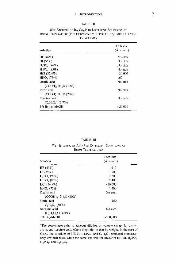
Many wet chemical solutions for InP are based on HCl, usually combined with H2O, H3PO4, HNO3, H2O2, or HBr. The etch rates are up to 5 /xm min~^ for HCl concentrations. Strong dilution with water is used to provide rates in the hundreds of angstroms per minute range for device fabrication. For selective etching, H2SO4/H2O2/H2O will etch InGaAs or InGaAsP, but stop on InP. In the reverse direction, HCI/H2O etches InP, but stops on InGaAs or InGaAsP.
Figure 4 shows the etch rates of InGaP in H3PO4/HCI/H2O mixtures (25 °C) as a function of the etch solution. This is a thermally activated etch with an activation energy of 11.3 kcal mol"^ for 1 : 1 : 1 solutions. The etch rates are controllable in the range 50-16,000 A min with this mixture. A mixture of HCI/H2O selectively etches AllnP from GaAs at rates 600-6000 A min"^ for formulations of 30:1 to 5:1 H2O to HCl (Fig. 5) and is thermally activated with a 12.4-kcal mol~^ activation energy (Fig. 6).
Compilations of results for wet etching of InQ5Gao5P and AlgsIUosP, the com-positions lattice-matched to GaAs, are given in Tables II and III, respectively.

1 INTRODUCTION
TABLE I
WET CHEMICAL ETCH MIXTURES FOR GaAs
Mixture Comments
H2SO4/H2O2/H2O
HNO3/H2O2/H2O
HCI/H2O2/H2O
H3PO4/H2O2/H2O
CH3COOH/HNO3/H2O2 NH4OH/H2O2/H2O NHO3/HF Km2/H20 K3Fe(CN),/K4Fe(CN),
Etch rate of up to 5 /Am min" for low dilution
Etch rate of up to 7 /jun min~^ for low dilution
HNO3 may be substituted for H2O2 and methanol substituted for H2O
Ethanol or methanol may be substituted for H2O
HCl often used in place of H2O2 PA etch, common in device fabrication Rapid etch usually diluted with H2O Selective for AlGaAs at low pH Can be made selective for GaAs or AlGaAs
HCl etches both materials, as does Br/MeOH, but HF, HI, H2, SO4, citric acid, and H3PO4 all provide selective etching for AllnP over InGaP.
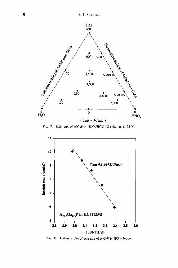
The HNO3/HCI/H2O solution provides both selective and nonselective etching for AlosGaQgP relative to GaAs, as shown in Figure 7. In pure HCl, AlGaP etches in a reaction-controlled mode (Fig. 8).
HCi 12,000
16,000
2000
H3PO4 0 0 0 H2O
FIG. 4. Etch rates of InGaP (in angstroms per minute) at 25 °C in H3PO4/HCI/H2O solutions.

S. J. PEARTON
fUUU
6000
\ 5000
°<, 4000
LU
< 3000
I
g 2000
1000
0
A^nP o 25'»C
1 1 1 1 1 1
5:1 10:1 15:1 20:1 25:1 30:1
CONCENTRATION RATIO (HgO : HC )
FIG. 5.
Selective dry etching for AlGaAs over GaAs has not been demonstrated and wet chemical etching is still being widely used in such material systems. KI/I2/H2O solution provides excellent selectivity (600 : 1) and fast etch rate (4 /x min"^ for AI02G08AS). This has been successfully appUed to gate recess etch for AlGaAs/GaAs base field effect transistors (FETs). There is a drawback
l U ^
^ c E
0 ^
UJ 103
I
LU
102
R oc e- a/kT ; V Eg = 12.36 kcal/mole
- N. A InP >Q
\ ^ M y
• \ .
>w 0
1 1 1 1 1
3.0 3.1 3.2 3.3 3.4 3.5 3.6
1000/T (K)
FIG. 6. Arrhenius plot of etch rate of AllnP in 2OH2O : IHCl.
1 INTRODUCTION
TABLE II
WET ETCHING OF 10256325? IN DIFFERENT SOLUTIONS AT
ROOM TEMPERATURE (THE PERCENTAGES REFER TO AQUEOUS DILUTION
BY VOLUME)
Etch rate Solution (A min"^)
HF (49%) No etch HI (55%) No etch H2SO4 (96%) No etch H3PO4 (95%) No etch HCl (37.4%) 20,000 HNO3 (75%) 160 Oxalic acid No etch
(COOH)22H20 (10%) Citric acid No etch
(COOH)22H20 (20%) Succinic acid No etch
(QH^OJ (6.7%) 1% Br2 in MeOH > 30,000
TABLE III
WET ETCHING OF ALINP IN DIFFERENT SOLUTIONS AT
ROOM TEMPERATURE''
Solution
HF (49%) HI (55%) H2SO4 (96%) H3PO4 (95%) HCl (34.7%) HNO3 (75%) Oxalic acid
(COOH)2-2H2O(20%) Citric acid
C^HgO^ (50%) Succinic acid
(C4H6O4) (14.3%) 1
''The percentages refer to aqueous dilution by volume except for oxalic, citric, and succinic acid, where they refer to that by weight. In the case of GaAs, the solutions of HF, HI, H3PO4, and C5H8O7 produced unmeasur-ably low etch rates, while the same was true for InGaP in HF, HI, H2SO4, H3PO4, and C6H8O7.
Etch rate (A min-^)
910 1,300 2,200 2,400
>50,000 1,400
No etch
250
No etch
> 100,000
/
/
§'
50
S. J. PEARTON
HCl 200
• It
4,000 7200
• 3,500
• 3,000
^ o <0k
\ ^
\ % > 20,000\ -v,
\ V \ '^ \ °/. 9
210
150
8,800 >30,000\
7,300
(Unit = A/min )
11
10
1 ®
I 1 7
6 A
Ea= 54.4±5KJ/mol
^ . 5 ^ ^ 0 . 5 ^ ^ HCl (12M)
I I \ I I I I
2.8 2.9 3.0 3.1 3.2 3.3 3.4 3.5 3.6
1000/T(1/K)
FIG. 8. Arrhenius plot of etch rate of AlGaP in HCl solution.
1 INTRODUCTION 9
of the etchant, however, in that wherever gold-based metalUzation is exposed to the etch solution it will be corroded [10]. Sometimes gold-based emitter metallization is preferred as the etch mask for emitter mesa definition in self-aligned processing. With a similar KI/I2 solution at an adjusted pH value, the reverse etch selectivity of GaAs over AlGaAs can also be achieved. The differ-ential etch rates of GaAs and Gaj.^Al^As as a function of the pH value provide selectivity. The etching selectivities increase with the increase of Al content from 8:1 for AlQ2Gao8As to 20:1 for Alo44GaQ56As. The recommended use of this etch is for a solution containing 0.3-M KI and 0.04-M I2 in a solution buffered to pH 8.7-9.3. The preferred buffer is a solution of borax with NaHC03 added to obtain the desired pH. NaHC03 is considered essential for this etch.
The K2Cr207/H3P04/H20 solution is a general etching solution for Al that contains III-V semiconductors, such as InAlAs or GaAlAs. The etch rates of GaAlAs rise rapidly as a function of the Al content, from ^^50 A min~^ at 10% Al to 320 A min~^ at 50% Al. Although this solution showed only a small selectivity of Ga . ^Al As over the AlGaAs/GaAs material system, the etch rate is quite slow (400 A min~^ at 26 °C) and can be easily handled and controlled in the emitter mesa definition process.
Relatively little success has been obtained in developing wet etch solutions for III-V nitrides [11, 12]. For AIN, a number of different solutions have been reported for amorphous or polycrystalline material. For example, hot (<85 °C) H3PO4 has been found to etch AIN deposited on Si by plasma-enhanced chem-ical vapor deposition at low rates (<500 A min~^) [13, 14]. A variety of other solutions, including hot (-100 °C) HF/H2O [15-17], HF/HNO3 [18], or NaOH [19], can etch sputtered or reactively evaporated amorphous AIN. For GaN, there were several early reports of wet etching in NaOH that progressed by formation of an insoluble gallium hydroxide (GaOH) coating [20, 21]. This film had to be removed by continual jet action. Other researchers have reported that H3PO4 will remove GaN at a very slow rate. For InN, aqueous KOH and NaOH solutions were found to produce etch rates of a few hundred angstroms per minute at 60 °C [22]. There has been particular difficulty in finding reliable wet etchants for single crystal nitrides.
We did not find any etchant for GaN or InN at temperatures below —80 °C. However, strong base solutions (KOH, NaOH, or photoresist developer, in which the active ingredient is KOH) were found to etch single crystal AIN at control-lable rates whose magnitude was strongly dependent on material quality.
Figure 9 shows a plot of etch rates in AZ400K photoresist developer as a function of the temperature for three different AIN samples.
1. Data designated by triangles are from polycrystalline AIN grown on GaAs. Etch rates for this material are much faster than for two single crystal samples grown on AI2O3 [23, 24].
2. Data designated by squares are from a l-)Ltm-thick layer with a double crystal X-ray diffraction peak width of 4000 arcsec.

10 S. J. PEARTON
12000
9000 I B 6000
I 3000 H
OH
High Quality AIN on AI2O3I
AIN on AI2O3
AIN on GaAs
0 25 50 75
Temperature (X) 100
FIG. 9. Etch temperature of different AIN samples in KOH-based solution as a function of temperature.
3. Data designated by circles are from material with a peak width ^200 arcsec.
The etching is thermally activated with an activation energy of '^ 15.5 kcal mol"^ in each case. This is consistent with reaction-limited etching, and the etch depth was also found to be a linear function of time with an absence of dependence on agitation. If the etching was diffusion-limited, we would expect an activation energy below ^^6 kcal m o r \ a ^/t dependence of etch on time, and a strong dependence of etch rate on degree of solution agitation. Higher rates for lower crystalUne quality materials are expected on the basis of a greater number of dangling or defective bonds that are attacked by the OH" ions in solution. Therefore, the successful attempt frequency is higher under these conditions and the etch rate R is higher. The process is well described by the relation
R = RQ exp kT
where RQ is the successful attempt frequency for breaking of an Al—N bond and formation of a soluble etch product, E^ is the activation energy (15.5 kcal mol~^), k is Boltzmann's constant, and T is the absolute temperature of the etch solution.
We have observed a strong effect of annealing on the subsequent wet etch rate of sputtered AIN films in KOH solutions, with over an order of magnitude decrease in rate after annealing at 1100 °C [25]. Similarly the etch rate for InQ2Alo gN grown on Si was approximately three times higher in KOH-based solutions than for material grown on GaAs, which is consistent with the superior

1 INTRODUCTION 11
FIG. 10. SEM micrographs of InGaAsP/InP microdisk lasers formed by nonselective dry etch.
crystalline quality of the latter. Etching of In^Ali_^N was also examined as a function of In composition, with etch rate initially increasing up to 36% In and then decreasing to zero for InN [25].
Other researchers have found that only molten salts (KOH, NaOH, P2O5) will etch GaN at temperatures above 300 °C, making handling and masking of material impractical.
Minsky, White, and Hu [26] reported laser-enhanced, room temperature wet etching of GaN using dilute HCI/H2O or 45% KOH/H2O, with rates up to a few thousand angstroms per minute for HCl and a few thousand angstroms per minute for KOH. The mechanism is believed to be photoenhancement of oxidation and reduction reactions in what amounts to an electrochemical cell. Etch rates were linearly dependent on incident HeCd laser power.
12 S. J. PEARTON
Zory et al. [27] employed a pulsed electrochemical cell combining 40 parts ethylene glycol, 20 parts water, and 1 part 85% H3PO4 to etch p-GaN and InGaN epitaxial layers at rates up to 1.5 ixm h~\ Cell voltage (220 V) was pulsed at 100 Hz (300 /xm s~ pulse width). This technique was used to fabricate a double heterostructure p-GaN/InGaN quantum well n-GaN light-emitting diode using a liquid contact.
An example of the extremely high selectivity achievable with wet etching is shown in the microdisks of Figure 10. In this case, dry etching is used to form small cylinders from InGaAsP/InP quantum well structures, and then HCl solution is used to undercut the InP buffer layer and substrate to leave the quantum wells suspended by a thin pedestal.
References
1. M. J. Howes and D. V. Morgan, Eds. "GaAs: Materials Devices and Circuits." Wiley, New York, 1985. R. E. Williams, "GaAs Processing Techniques." Artech House, Dedham, MA, 1990. V. Swaminathan and A. T. Macrander, "Materials Aspects of GaAs and InP Based Structures." Prentice-Hall, Englewood Cliffs, NJ, 1991. S. J. Pearton, C. R. Abemathy, and F. Ren, "Topics in Growth and Device Processing of HI-V Semiconductors." World Scientific, Singapore, 1996. Ali and A. Gupta, Eds., "HEMTs and HBTs." Artech House, Boston, 1991. M. Shur, "GaAs Devices and Circuits." Plenum, New York, 1987.
2. S. Nakamura, T. Mukai, and M. Senoh, Appl. Phys. Lett. 64, 1687 (1994). 3. S. Nakamura, M. Senoh, S. Nagahama, N. Iwasa, T. Yamada, T. Matsushita, H. Kikoyu, and
Y. Sugimoto, Jpn. J. Appl Phys. 35, L74 (1996). 4. S. Nakamura, M. Senoh, S. Nagahama, N. Iwasa, T. Yamada, T. Matsushita, H. Kikoyu,
Y Sugimoto, T. Kozaki, H. Umemoto, M. Sano, and K. Chocho, Appl Phys. Lett. 72, 2014 (1998).
5. S. K. Gyhandi, "VLSI Fabrication Principles, Si and GaAs." Wiley, New York, 1983. 6. C. I. H. Ashby, EMIS Data Reviews, INSPEC, London, pp. 655-658. 7. D. W. Shaw, J. Electrochem. Soc. 118, 958 (1966). 8. S. Adachi and K. Oe, / Electrochem. Soc. 130, 2427 (1983). 9. S. lida and K. Ito, J. Electrochem. Soc. 118, 768 (1971).
10. R. S. Christ, "Proceedings of the U.S. Conference on GaAs Manufacturing Technology," p. 44. IEEE Press, New York, 1989.
11. S. J. Pearton, C. R. Abemathy, F Ren, J. R. Lothian, P Wisk, and A. Katz, J. Vac. ScL Technol, A 11, 1772(1993).
12. D. Walker and W. H. Tarn, Eds., "CRC Handbook of Metal Etchants." CRC Press, Boca Raton, FL, 1991.
13. T. Y Sheng, Q. Lu, and G. J. Collins, Appl Phys. Lett. 52, 576 (1988). 14. T. Pauleau, J. Electrochem. Soc. 129, 1045 (1982). 15. K. M. Taylor and C. Lenie, J. Electrochem. Soc. 107, 308 (1960). 16. G. Long and L. M. Foster, / Am. Ceram. Soc. 42, 53 (1959). 17. N. J. Barrett, J. D. Grange, B. J. Sealy, and K. G. Stephens, / Appl Phys. 57, 5470 (1985). 18. C. R. Aita and C. J. Gawlak, J. Vac. Scl Technol, A 1, 403 (1983). 19. G. R. Kline and K. M. Lakin, Appl Phys. Lett. 43, 750 (1983). 20. T. L. Chu, /. Electrochem. Soc. 118, 1200 (1971). 21. J. I. Pankove, / Electrochem. Soc. 129, 1045 (1972). 22. A. X. Guo, O. Kato, and A. Yoshida, J. Electrochem. Soc. 139, 2008 (1992). 23. J. D. MacKenzie, C. R. Abemathy, S. J. Pearton, V. Krishnamoorthy, S. Bharatan, K. S. Jones,
and R. G. Wilson, Appl Phys. Lett. 67, 253 (1995).

1 INTRODUCTION 13
24. C. R. Abemathy, Mater. ScL Eng., R 14, 203 (1995). 25. C. B. Vartuli, S. J. Pearton, J. W. Lee, C. R. Abemathy, J. D. MacKenzie, J. C. Zolper, R. J.
Shul, and F. Ren, 7. Electwchem. Soc. 143, 3681 (1996). 26. M. S. Minsky, M. White, and E. L. Hu, Appl. Phys. Lett. 68, 1531 (1996). 27. R L. Zory, J. S. Oh, and D. R. Bour, Proc. SPIE-Int. Soc. Opt. Eng. 3002, 117 (1996).

This Page Intentionally Left Blank

SEMICONDUCTORS AND SEMIMETALS, VOL. 73
CHAPTER 2
Gallium Arsenide Heterostructures
Eric Donkor
DEPARTMENT OF ELECTRICAL AND COMPUTER ENGINEERING, UNIVERSITY OF CONNECTICUT,
STORRS, CONNECTICUT, USA
INTRODUCTION 15
1.1. Growth of GaAs Heterostructures 17 1.2. Material Characterization 21 CRYSTAL GROWTH AND PROPERTIES OF GAAS 22
2.1. Crystal Growth 22 2.2. Impurities and Deep Levels 24 2.3. Crystal Structure and Lattice Properties 24 2.4. Electronic and Electrical Properties 27 GROWTH AND MATERIAL PROPERTIES OF GAAS HETEROSTRUCTURES 30
3.1. Introduction 30 3.2. Critical Thickness of Strained-Layer Quantum Wells 31 3.3. Heterostructures of the Type III-V/GaAs 32 3.4. Heterostructures of the Type III^-III^_^-V/GaAs 35 3.5. Heterostructures of the Type III-V^-Vy_JGaAs 46 3.6. Heterostructures of the Type (III^-IIIi_Jy-IIIi_y-V/GaAs 47 3.1. Heterostructures of the Type lll^-m^_^-Wy-W^_/GaAs 47 PHYSICAL PROPERTIES OF GAAS-BASED
QUANTUM WELL STRUCTURES AND SUPERLATTICES 48
4.1. Introduction 48 4.2. Quantum Wells Energy Levels 50 REFERENCES 55
1. Introduction
Gallium arsenide (GaAs) heterostructures are ultrathin heteroepitaxial layers of binary, tertiary, quaternary, or quinary III-V semiconductor alloys grown on GaAs substrates. The semiconductor heterostructure concept was first presented by Kroemer [1] in 1963 and rapidly developed in the 1970s [2^ ] . In 1970, Esaki and Tsu [5] predicted that such a structure has quantization of the elec-tronic energy states, hole energy states, and density of states. One of the early experimental demonstrations of the quantum-mechanical characteristics of GaAs heterostructures was reported by Dingle et al. [6] and a year later by Chang et al. [7].
15 Copyright © 2001 by Academic Press
All rights of reproduction in any form reserved. ISBN 0-12-752182-8
ISSN 0080-8784/01 $35.00

16 ERIC DONKOR
Heterostructures are commonly classified into single quantum wells (SQWs), double quantum wells (DQWs), multiple quantum wells (MQWs), and super-lattices (SLs). A SQW is formed between smaller bandgap and wider bandgap materials. A DQW is formed if the smaller bandgap semiconductor is sand-wiched between wider bandgap materials. If multiple quantum wells (QWs) are stacked together, the structure formed is a MQW or SL. A SL is formed if the layers are so thin that carriers are able to tunnel from well to well.
If the QW width is less than the de Broglie wavelength of the carriers, which is about 100 A in GaAs, then the electrons and holes can be spatially confined into two, one, or zero dimensions. A two-dimensional carrier confinement sys-tem is termed a quantum well structure, a one-dimensional carrier confinement system is called a quantum wire structure, and a zero-dimensional carrier con-finement system is called a quantum dot structure. Carrier confinement can be achieved either by an electrostatic potential created by delta doping, by modu-lation doping, or by virtue of the band offset at the heterointerfaces.
Evolution of GaAs heterostructure electronic devices began in 1980 when Mimura et al. [8] succeeded in developing a high electron mobility transistor. Shortly thereafter, Delagebeaudeuf et al. [9] and Solomon and Morkoc [10] pub-lished their versions named two-dimensional electron gas FETs and modulation-doped field effect transistor, respectively. Since then many new heterostructure field effect transistors (HFETs) have evolved. Some of the new devices are quite different in detail from the conventional HFET. The motivation for improve-ment is mainly the need for high-current-drive field effect transistors (FETs) for digital electronics, high-current-high-breakdown-voltage power FETs, and low-noise microwave and millimeter-wave FETs.
The heterojunction bipolar transistors (HBTs) form another major class of heterostructure electronic devices that was first reported by Kroemer [11, 12]. The unique feature of HBT is the use of a wide bandgap emitter and a smaller bandgap base. Thus, a band offset is produced at the emitter-base heterointer-face that favors electron injection into the base and retards hole injection into the emitter. In addition, the base of the HBT is heavily doped, resulting in mini-mization of the device parasitics and increased current gain [13]. Consequently, the HBT has greater high-frequency response.
Gallium arsenide heterostructure-based optoelectronic devices can be laser sources, photodetectors, and modulators. Heterostructure lasers are more perva-sive. They are classified as short wavelength (0.6-0.98-)Ltm), long wavelength (1.3-1.6-/>tm), and very long wavelength (2.0-30-/im) lasers [14]. An alternative classification scheme for heterostructure lasers is based on the nature of carrier confinement [15]. This leads to single quantum well lasers, multiple (includ-ing double heterojunction) quantum well lasers, separate confinement quantum well lasers, which provide different confinement for carriers and photons, and graded-index separate confinement quantum well lasers.
Gallium arsenide heterostructure-based photodetectors [16, Chap. 11; 17] transform electromagnetic radiation into electrical signals. They offer high

2 GALLIUM ARSENIDE HETEROSTRUCTURES 17
speed, high sensitivity, high quantum yield, and low intrinsic noise perfor-mances. Gallium arsenide heterostructure photodetectors that rely on interband transitions in quantum well structures are often designed for the visible region, whereas those that utilize intersubband transitions are designed to operate in the mid and far infrared region.
The most common heterostructure-based electrooptic modulator is the self-electrooptic effect device (SEED) [18]. The SEEDs operate on changes in the optical absorption induced by an electric field normal to the growth direction of the heterostructure [19], according to the Franz-Keldysh effect [20, 21]. The quantization effect in quantum well structures causes the resulting absorption spectrum to have large discrete steps. The wavelengths of these absorption steps shift when the quantum well structure is placed under the influence of an electric field. Furthermore, distinctive peaks exist in the absorption spectrum of quantum wells. These peaks also shift upon the application of an electric field. This peak shift is called the quantum confined Stark effect, which is the basic phenomenon underlying the operation of the more common heterostructure-based electrooptic modulators.
1.1. GROWTH OF GAAS HETEROSTRUCTURES
7.7.7. Metal-Organic Chemical Vapor Deposition Growth
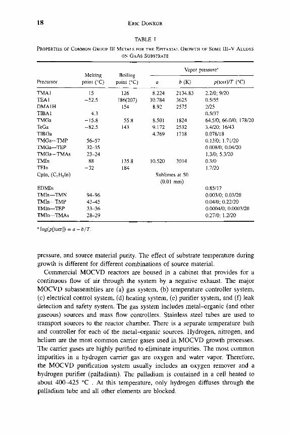
Metal-organic chemical vapor deposition (MOCVD) has evolved as a major technology [22-25] for the growth of GaAs heterostructures. The layers are grown by transporting different precursors or reactants in the vapor phase, under controlled pressure, into a reactor (vertical, horizontal, or barrel) cham-ber [26, 27] that holds the semi-insulating GaAs substrate. Alkyls of the group III metals and hydrides of the group V elements are typical precursors. Tables I and II list some common group III and group V precursors and their properties.
Three techniques have been introduced to improve the MOCVD growth pro-cesses: plasma-enhanced (PE-MOCVD) [28], atomic layer epitaxy (ALE) [29], and low-temperature (LT-MOCVD) [30] methods. In the PE-MOCVD growth, the plasma induces precracking of the precursors into the various con-stituents, thereby facilitating the controlled incorporation of the different chem-ical elements in the alloy formation at lower temperatures. In ALE growth, the substrate is separately and alternatively exposed to the precursors containing the group III and group V elements. This alternation allows for better control of the growth process at the monolayer level. In LT-MOCVD growth, the growth rate of the layers is less dependent on temperature. Thus the growth rate can be held constant during the process. This enables layers to be grown with uniform thick-ness and composition, and interfaces have abrupt compositional changes. Key parameters that affect the MOCVD growth characteristics include the substrate orientation and preparation, flow rate of the precursors, growth temperature.
18 ERIC DONKOR
TABLE I
PROPERTIES OF COMMON GROUP III METALS FOR THE EPITAXIAL GROWTH OF SOME I I I - V ALLOYS
ON GAAS SUBSTRATE
Precursor
TMAl TEAl DMAIH TIBAl TMGa TeGa TIBGa TMGa—TMP TMGa—TEP TMGa—TMAs TMIn TEIn Cpin, {C,U,ln)
EDMIn TMIn—TMN TMIn—TMP TMIn—TEP TMIn—TMAs
Melting point (°C)
15 -52.5
4.3 -15.8 -82.5
56-57 32-35 23-24 88
-32
94-96 43-45 33-36 28-29
Boiling point (°C)
126 186(207)
154
55.8 143
135.8 184
a
8.224 10.784 8.92
8.501 9.172 4.769
10.520
Vapor
biK)
2134.83 3625 2575
1824 2532 1718
3014
Sublimes at 50 (0.01 mm)
pressure"
p(torr)/r (°C)
2.2/0; 9/20 0.5/55 2/25 0.5/37 64.5/0; 66.0/0; 178/20 3.4/20; 16/43 0.078/18 0.13/0; 1.71/20 0.008/0; 0.04/20 1.3/0; 5.3/20 0.3/0 1.7/20
0.85/17 0.003/0; 0.03/20 0.04/0; 0.22/20 0.0004/0; 0.0003/20 0.27/0; 1.2/20
^\og(p[tOTT]) = a-b/T.
pressure, and source material purity. The effect of substrate temperature during growth is different for different combinations of source material.
Commercial MOCVD reactors are housed in a cabinet that provides for a continuous flow of air through the system by a negative exhaust. The major MOCVD subassemblies are (a) gas system, (b) temperature controller system, (c) electrical control system, (d) heating system, (e) purifier system, and (f) leak detection and safety system. The gas system includes metal-organic (and other gaseous) sources and mass flow controllers. Stainless steel tubes are used to transport sources to the reactor chamber. There is a separate temperature bath and controller for each of the metal-organic sources. Hydrogen, nitrogen, and helium are the most common carrier gases used in MOCVD growth processes. The carrier gases are highly purified to eliminate impurities. The most common impurities in a hydrogen carrier gas are oxygen and water vapor. Therefore, the MOCVD purification system usually includes an oxygen remover and a hydrogen purifier (palladium). The palladium is contained in a cell heated to about 400-425 °C . At this temperature, only hydrogen diffuses through the palladium tube and all other elements are blocked.

2 GALLIUM ARSENIDE HETEROSTRUCTURES 19
TABLE II
PROPERTIES OF COMMON GROUP V METALS FOR THE EPITAXIAL GROWTH OF SOME I I I - V ALLOYS
ON GAAS SUBSTRATE
Precursor
P PH3 TMP TEP IBP TBP AS
ASH3 TMAs TEAS
DMAs DEAs TBAs PhAsH2 TMSb TESb TMBi
Melting point (°C)
-84 -88( -85)
- 2 0 4
-87.3
- 1
-87.6 -98
-107.7
Boiling point (°C)
38 127 78 54
-62.5 50
140
36.3 102 65
80.6 160 110
a
7.7627 8.035 7.578 7.586
7.3936
7.532 7.339 7.243 8.47 7.7068
7.628
Vapor pressure''
biK) p
1518 2065 1648 1539
1456
1443 1680 1509 2410 1697
1816
(torr)/r (°C)
1/260
0.5/55 46.5/50 112/25 141/10 1/370
238/20 5/20
15.5/37 176/0 40/20 81/10 1.8/20
4/25 27/20
Mog(/7[torr]) = a-Z7/r .
The metal-organic sources are contained in stainless steel cylinders equipped with a temperature controlled bath. Commercial temperature control baths are capable of temperature control, using a thermocouple element, over a wide range from about - 2 0 to 100 °C at ±0.01% accuracy. Precisely controlling the temperature regulates the partial pressure of the source. Electronic mass flow controllers control the exact amount of carrier gas flowing through the bubblers and at the same time maintain a constant vapor pressure of the source.
A heating system heats the substrate during growth. The heater can raise the temperature of the substrate to about 1000 °C. Heating can be achieved by radiofrequency (rf) induction heating, radiative heating, and resistance heating. Radiofrequency heating is common in large commercial systems. In this type of heating, the substrate susceptor is inductively coupled to the rf coil. In radiative heating, the heat energy from a resistance element is transformed into radiant energy. The susceptor absorbs the radiant energy and converts it back to heat energy. In the resistance heating method, current flows through an electrically conductive layer mounted to the susceptor to generate the required heat energy. Safety precautions include gas leak detectors for the carrier gas, the purifier, and toxic gases. Commercial MOCVD are computer controlled, and can be used to define the growth process and to monitor reactor conditions.

20 ERIC DONKOR
7.7.2. Molecular Beam Epitaxy Growth
Figure 1 shows the basic components of a multichamber ultra high vacuum molecular beam epitaxy (MBE) system [31]. It consists of growth chamber, wafer loading and preparation chamber, and analytical chamber. The growth chamber, which usually has a 450-mm inner diameter, holds a removable source flange that provides support for effusion cells, their shutters, and their liquid nitrogen (LN2) shroud. The cells are oriented such that their beams converge on the substrate in the growth position. The beam sources are thermally isolated from each other by an LN2 cooled radial vane baffle, which prevents chemical cross-contamination. A second cryopanel surrounds the substrate such that the stainless steel bell jar is internally lined by this cryopanel for the purpose of reducing contamination due to outgassing of the chamber walls. The sample preparation and loading chamber is connected to the growth chamber via large diameter channels and isolation valves. The analytical chamber allows for in situ and postgrowth surface analysis without exposing the sample to outside environments.
The substrate surface must be prepared prior to epitaxial growth. Preparation of the surface entails preloading chemical treatment as well as in situ cleaning processes. The goal of the preloading chemical treatment is to provide either a clean chemical oxide layer of a few angstroms thick on the GaAs substrate
GROWTH CHAMBER
Bectron diffraction gun 10-50 ktV
Transfer rod
Electron analyser (AES.LEELS.ESCA)
WAFER LOADING AND PREWVRATION CHAMBERS
FIG. 1. Schematic diagram of an MBE system showing the growth chamber, the wafer loading and preparation chambers, and the analytical chamber for surface analytical studies. Reproduced with permission from K. Ploog, "Springer Proceedings in Physics" (G. Lelay, J. Derrien, and N. Boccara, Eds.), Vol. 22, p. 10. ©1987 Springer-Verlag, New York.

2 GALLIUM ARSENIDE HETEROSTRUCTURES 21
surface or hydrogen passivation of the GaAs surface. An approach for GaAs surface preparation was described by Drummond et al. [32]. The first step is polishing of the substrate surface to mirror finish. One approach is to use pellon cloth saturated with Br—CH3OH. This is followed by wet chemical cleaning of the substrate in a 3 : 1 : 1 solution of H2SO4 : H2O2: H2O for about 10 min to remove organic contamination. The wafers are then degreased, etched again in H2SO4 : H2O2: H2O, and rinsed in deionized water.
Next the substrate is loaded into the airlock high vacuum growth chamber. The pressure of the growth chamber is typically 10"^ torr. The growth chamber is equipped with liquid nitrogen shrouds that surround the effusion cells and the substrate, and line the walls of the chamber. The purpose of the shrouds around the effusion cells is to prevent excessive heating of the chamber, espe-cially around the ovens, which can lead to contamination due to desorption of unwanted residues. The shrouds that surround the substrate and line the walls condense residual gases and water vapor, especially those desorbed by the sub-strate heater, and remove any fluxes. An ionization gauge situated behind the substrate block, which is mounted in the growth chamber, monitors the As flux and a high-energy electron diffraction (HEED) system.
The shrouds are filled with liquid nitrogen well before growth is initiated and are kept on until the furnace temperatures are reduced after growth. Once the chamber has been chilled, the effusion cells are turned on and stabilized to the desired temperature with a dc current, controlled by a temperature controller (W-5%ReAV-26%Re) thermocouple. Likewise, the substrate surface is heated to about 630 °C. The HEED pattern is closely monitored to ensure that the native oxide layer is completely desorbed off the substrate at a precise temper-ature, say 580 °C. The substrate temperature is subsequently raised or lowered to the growth temperature. Once the desired growth temperature is reached, the shutters for the appropriate effusion cells are opened, followed by opening of the main shutter to initiate epitaxial growth. The initiation of the thin film is moni-tored by the HEED pattern. A commercial MBE facility is shown in Figure 2. The system is designed for the growth of GaAs-based heterostructure devices, optoelectronic devices, and integrated circuits.
1.2. MATERIAL CHARACTERIZATION
The Hall effect is the most basic characterization technique for evalu-ating semiconductor heterostructures. It is used to determine the type and concentration of elements in a sample. It can also allow for determination of the electrical activation energy for donors and acceptors in GaAs and its alloys by analyzing ionized impurity scattering and its effect on carrier mobility. The mea-surement techniques are well established and widely reported in the literature [33].

22 ERIC DONKOR
FIG. 2. A commercial MBE system used for the growth and analysis of GaAs heterostructure materials and devices at the University of Connecticut.
Characterization of heterolayers based on techniques that give structural infor-mation include transmission electron microscopy, X-ray diffraction, scanning tunneling microscopy, and those that give information on the band structure. The latter comprise optical measurements such as photoluminescence excitation spectroscopy, absorption and reflectivity, and electrical measurements such as Hall and Shubnikov-de Haas measurements.
Etching has been employed to characterize the structural and chemical inho-mogeneities in semiconductors [34-36]. The structural and chemical defects are observed indirectly from their effects on the etching mechanism. Etching also has been used to study defects such as dislocations and staking faults [37]. The major drawback of this technique is that it resorts to destructive testing.
2. Crystal Growth and Properties of GaAs
2.1. CRYSTAL GROW^TH
The MOCVD growth of GaAs results from the reaction between group III alkyls (e.g., TMGa, TEGa) and group V hydrides (e.g., ASH3, TEAs). The

2 GALLIUM ARSENIDE HETEROSTRUCTURES 23
reaction takes place in a reactor chamber that contains a semiinsulating GaAs substrate placed on a heated carbon susceptor. Typically growth temperatures range between 575 and 700 °C, and depend on the precursors used. Highest purity material, using TMGa and ASH3, has been achieved [21, 22] in the tem-perature region from 600 to 650 °C. The chemical reactions that lead to the formation of GaAs from metal-organic precursors is a complex process that is not fully understood. The reactions break down into gas-phase reactions and surface reactions [38, 39]. The gas-phase reactions involve multiple pyrolytic decompositions of organometallics and reactions with hydrogen radicals [40-42]. The surface reactions entail decomposition, surface adsorption, and des-orption. Volatile by-products are removed from the surface by adsorption, by colliding gas-phase radicals, and by bimolecular surface recombination.
One major problem with the group III sources is the unintentional doping of the layers with carbon [43-45], making the alloy effectively p type [46]. How-ever, GaAs grown from TEGa and ASH3 turn out to have lower carbon contam-ination. The ratio of group V to group III also affects the quality of the alloy growth. At low V: III values the GaAs is p type, having high carbon concen-trations. The carbon concentration decreases with increasing V : III ratio, and at a critical ratio the GaAs material becomes semi-insulating. The substrate orien-tation also affects the introduction of carbon. The (111) and (311) orientations show lesser carbon incorporation, but (100) is the preferred substrate orientation because it yields the best surface morphologies and cleaves easily.
The MBE growth of GaAs occurs through the interaction of Ga atoms and As2 (and/or AS4) molecules impinging on a GaAs substrate [47, 48]. Most recent developments use gas sources and are variously known as gas-source molecular beam epitaxy, chemical beam epitaxy, or metal-organic molecular beam epitaxy (MOMBE). In this case the growth occurs between TMGa (or TEGa) and ASH3. The sticking coefficient of Ga atoms must approach unity, with condensation of As2 via bonding with Ga [49, 50] for growth to occur. The sticking coefficient of As2 increases as the ratio of Ga flux to AS2 flux ((/>Ga/ As2) increases, reaching unity when (t)Q^ = 24>j^^^. This situation implies that stochiometric formation of GaAs can occur for (J)Q^ < 24>^^^ and the excess AS2 is lost by desorption.
The layer by layer growth of GaAs by MBE or MOCVD results in surface reconstruction, that is, a surface that is different from the "native" surface of the material. The surface may reconstruct so that surface atoms care share bonds. This reconstruction results in a two-dimensional symmetry with periodicity dif-fering from that of the underlying atoms of the GaAs crystal. The surface atoms may also relax, that is, change the bond angles, but not the number of nearest neighbors, to seek new equilibrium positions. The reconstructed GaAs surface has variety of structures. These are the (1 x 1) structure of the (110) face, (2 x 2) structures of the (111) and ( i l l ) faces, and a series of structures [c(4 x 4), c(2 X 8), c(8 X 2), p{\ X 6), p{A x 6), etc.]. The letter "p" indicates that the unit cell is primitive and "c" indicates that the unit cell has an additional scatter in the center.

24 ERIC DONKOR
The GaAs surface structure has been studied using a variety of tech-niques such as reflection anisotropy spectroscopy (RAS) spectra for MBE- and MOCVD-grown (001) GaAs [51, 52]. The RAS method is based on the fact that a cubic material such as GaAs is optically isotropic in first-order reflectivity. Thus anisotropic reflectivity originates from the surface with different symme-tries. A more common method for surface measurement is the low-energy elec-tron diffraction (LEED) method. In LEED, electrons of well defined energy and direction diffract from the crystal surface. The low-energy electrons are scat-tered mainly by individual atoms on the surface and produce a pattern of spots on a fluorescent screen. The spots in the pattern correspond to the points in the two-dimensional reciprocal lattice.
2.2. IMPURITIES AND DEEP LEVELS
A number of elements are electrically active impurities in GaAs and pro-duce shallow donor or acceptor levels [53]. Deep levels due to impurities or lattice defects [54] also exist. Table III gives a summary of some of the impu-rities, their activation energies, and their diffusion in GaAs. The most common dopants for MBE-grown GaAs are Be for p type and Si, Ge, and Sn for n type. Beryllium acts as an acceptor in MBE-grown GaAs [55]. Abrupt doping levels can be achieved due to the low diffussivity of Be in MBE-grown GaAs [56]. At substrate temperature exceeding 550 °C and at high doping levels above 5 X 10 ^ cm"- , the surface morphology degrades [57] and the diffusion of Be is enhanced [58, 59], resulting in degradation of the doped epitaxy. On the other hand, lowering the substrate temperature to 500 °C lowers the diffusivity of Be and acceptor levels of 2 x 10 ^ cm~^ can be achieved [60].
Silicon is the most commonly used n-type dopant in MBE-grown GaAs. It is incorporated on Ga sites under As-stabilized conditions and yields n-type mate-rial. Germanium is an amphoteric dopant and it can be used to prepare either p-or n-type films, depending on the growth condition [61, 62]. Germanium acts as an acceptor on As sites and as a donor on Ga sites. The site substitution depends critically on the As: Ga flux ratio and on substrate temperature. Figure 3 [31, p. 27] gives doping concentrations for Si, Be, Ge, and Sn in MBE-grown GaAs, as a function of temperature for a constant growth rate of 1 /jum/h [31].
2.3. CRYSTAL STRUCTURE AND LATTICE PROPERTIES
The GaAs crystal structure has been studied and reported extensively [63]. It has a zincblende crystal structure with a lattice constant, QQ, that is temperature dependent as shown in Figure 4 [64]. The nearest-neighbor configurations are such that each Ga species is surrounded by four As species and vice versa, with a nearest-neighbor bond length of r^ = {V^UQ/A) = 2.44793 A at 300 K,

6.0^5.89^ 6.0^5.85^ 3.0«
,5.845'-, ,5.812^
5.808\5.799^ 5.817^ 5.908^5.949^ 5.773^ 5.937^
24^30.7^ 2^,34.7^^ ly 80^40.4^ 12«,28.8^ 28^
,5.87^ ,5.789'
, 5.839^
,5.888^
2 GALLIUM ARSENIDE HETEROSTRUCTURES 25
TABLE III
ACTIVATION ENERGIES OF IMPURITIES AND THEIR DIFFUSION IN GAAS
Element Activation energy (meV)
Shallow donors S Se Te Si Sn Ge Pb C
Shallow acceptors Zn Cd Li Ge Mg Be
«S. M. Sze and J. C. Irvin, Solid State Electron. 11, 599 (1968). ^C. M. Wolfe et al., Conf. Ser. Inst. Phys. 33b, 120 (1977). ' M. Ozeki et al., Conf. Ser. Inst. Phys. 45, 220 (1979). ' A. G. Milnes, Electron. Electron Phys. 61, 63 (1983). "U. Kaufmann and J. Schneider, Electron. Electron Phys. 58, 81 (1982).
and a bond angle of 109.47°. Gallium arsenide cleaves most readily on {110} family planes, but can also cleave on {111} planes and between (111) and (011). Of the eight planes in the {111} family, four {111A} planes contain only Ga atoms and four {1115} contain only As atoms. These two planes have different chemical activity and behavior [65, 66]. The elastic properties of GaAs include compliance and second- and third-order moduli. The small-stress second-order moduli have only three independent components [67]. The shear modulus, bulk modulus. Young modulus, Poisson ratio, isotropy ratio, Cauchy ratio, and Bom ratio are determined from the second-order moduli with the use of the formulae [63, p. 3] indicated in Table IV.
The speed of nondispersive or (long-wavelength) bulk acoustic waves can be expressed in terms of the second-order moduli and the crystal density [63, p. 3], and is given for the high-symmetry [100], [110], and [HI] directions as Hsted in Table V. The room temperature phonon dispersion curve reported by Waugh and Dolling [68] is represented graphically in Figure 5. The data are the wave vectors along the [100], [110], and [111] directions.

26 ERIC DONKOR
TEMPERAIURe CO
1100 KXK) 900 800 700 600 500
10 07 0.8 1.2 1.3 09 1.0 1.1 1000/T (K-M
FIG. 3. Room temperature carrier concentration in MBE-grown GaAs as a function of effusion cell temperature for Si, Ge (n-type), Be, and Sn. The data were obtained from Hall effect and capacitance-voltage measurements at constant growth rate, substrate temperature, and AS4 : Ga flux ratio. Reproduced with permission from K. Ploog, "Springer Proceedings in Physics" (G. Lelay, J. Derrien, and N. Boccara, Eds.), Vol. 22, p. 10. ©1987 Springer-Verlag, New York.
FIG. 4. Variation of lattice constant versus temperature for stoichiometric, Ga excess, and As excess MBE-grown GaAs. Reproduced with permission from O. Madelung, "Data in Science and Technology: Semiconductors," p. 104. ©1991. Springer-Verlag, New York.

2 GALLIUM ARSENIDE HETEROSTRUCTURES 27
TABLE IV
FORMULAE FOR ACOUSTIC AND MECHANICAL PROPERTIES OF GAAS
Parameter Formula
Shear modulus Cu C,2
2 c Xic
Bulk modulus 5 , = -^ 3
Young Modulus along [100] Y, = (<^.i+2Q2)(Qi - Q2) ^11 + ^ 1 2 c,
Poisson ratio along [100] PQ = ^ 1 1 " ^ ^ 1 2
C — C T Isotropic ratio /, = —^ —
2C44
Cauchy ratio Q =
Bom ratio Br. =
C44
(Cii+C|,)^ 4 L I I (Cj i — C44)
TABLE V
SPEED OF ACOUSTIC WAVES IN GAAS
Parameter
VL
Vr
V/
^ r | |
Vrl
VL/
Vn
Wave propagation direction
[100] [100] [110] [110] [110] [111] [111]
Direction or plane of particle motion
[100] (100) plane [110] [001] [110] [111] (lll)plane
Wave speed (
7 = 300 K
4.731 ±0.005 3.345 ±0.003 5.238 ±0.008 3.345 ±0.003 2.476 ±0.005 5.397 ±0.008 2.796 ±0.006
xlO^ cm/s)
r = 77 K
4.784±0.015 3.350 ±0.005 5.289±0.015 3.350 ±0.005 2.479±0.012 5.447 ±0.015 2.799±0.015
2.4. ELECTRONIC AND ELECTRICAL PROPERTIES
Figure 6 shows the general features of the electron energy versus reduced wave vector for the valence band and a number of conduction bands for GaAs as calculated via a nonlocal empirical pseudopotential method by Chelikowsky and Cohen [69]. Gallium arsenide has a direct energy gap {E^ = Fg — F ) of 1.424 eV at 300 K. The spin-orbit interaction splits the T^^ valence band into Fg and F^, where the splitting energy difference is represented by AQ. Likewise the F{5 conduction band splits into T^ and F with a splitting energy difference given by AQ. The spin-orbit interaction also splits the L'^iA'^) valence band into LlJAl,) and L (A,").

28 ERIC DONKOR
0 0^ 0.4 0.6 0.8 IJO I.O as 0.6 0.A 0.Z 0 0 01 0.2 0.3 a4 as
[qOOl [Oqql (qqq)
REDUCED (DIMENSIONLESS) WAVE-VECTOR, q
FIG. 5. GaAs acoustic and optical branch phonon dispersion relation. The experimental points (•, A, o, A, D) were determined by Waugh and Dolling [68] by elastic neutron scattering, and the theoretical curves are represented by solid and dotted lines. The dashed lines near q ^' 0,v -^ 0 represent the initial slopes for the various speeds of sound. Reproduced with permission from O. Madelung, "Data in Science and Technology: Semiconductors," p. 104. ©1991. Springer-Verlag, New York.
>-o
z UJ
L A r A X u.K I r REDUCED WAVE VECTOR q
FIG. 6. Electronic band structure calculated by Chelikowsky and Cohen from a nonlocal empirical pseudopotential method. Reproduced with permission from J. R. Chelikowsky and M. L. Cohen, Phys. Rev. B 14, 555 (1976). © American Physical Society, New York.

2 GALLIUM ARSENIDE HETEROSTRUCTURES 29
The electronic effective masses m^ at the conduction band minima a (= r , Z, or L) based on density-of-states calculations is given by
< = A^2/3^2/3^./3 (2.1)
where A is the number of equivalent minima, and m^^ and m ^ are the trans-verse and longitudinal masses of the minima. For conductivity calculations, the conductivity effective mass m" is used:
_L.lfA+M (2.2)
Determination of electronic effective mass at the high-symmetry points is derived from the k • p approach, which gives the expression [70]
—^ = 1 + — m\ ^ 3
3
2 1 —+ ^0 ^0 "I" ^ 0 J
+ ^ . (2-3)
where m^ is the free electron mass, ? is the momentum matrix element con-necting the p-like valence band with the s-like conduction band, and P' is the momentum matrix element connecting the s-like conduction band with the next higher lying bands.
The effective density-of states hole mass, m^, at the valence band is given by the expression
. 2 / 3
(2.4) \m^^^rm\!^\
where the heavy-hole mass m^ = 0.5Imo and 0.50mo at T = 0 and 300 K, respectively, and the Hght-hole mass m,h = 0.082mo and 0.0.076mo at T = 0 and 300 K, respectively, where m^ represents the electronic mass.
The effective electron mobility depends on scattering-limited mechanisms, such as polar optical scattering, acoustic phonon scattering, piezoelectric scatter-ing, intervalley scattering, impurity scattering, electron-electron scattering, and alloy scattering. At low fields, the electrons in GaAs occupy the lowest con-duction band minima, F of the zone center. Using Mattiessen's rule [71, 72] the total mobility is expressed as the sum of the scattering rates of the domi-nant scattering process polar optical scattering [i^ and impurity scattering /!„. Expressions for the polar optical scattering-limited mobility and the impurity scattering-limited mobility were given by Ehrenreich [60, 73, 74] and Brooks-Herring [75], respectively, as
xMHG(z)[exp(z)- l ] (2.5)

30 ERIC DONKOR
M„-3 .28x lO '> - i—^-[\n{\+b)-(mVmo)^Af,V 1 + ^
(2.6)
b . '•^^-'^'%'-'T' (2.7)
n' = n + {No-N^-n)^^ (2.8)
A ,. = « + 2A ^ (2.9)
Here T is the temperature in kelvin, e is the electronic charge, and * is the Callan effective charge (and e""/e = 0.20), M is the reduced mass of the cell that equals 5.92 x 10 ^ kg, 11 = 5.05 x 10"^^ m^ is the volume of the primitive cell, 0 is the polar phonon temperature, z = 0/T, G{z) is a screening factor [60], n is the electron density, k^ is the static dielectric constant, and A/ , and A^ (per cubic centimeter) are the donor and acceptor densities, respectively.
3. Growth and Material Properties of GaAs Heterostructures
3.1. INTRODUCTION
Epitaxial layers of GaAs-based heterostructures are binary, tertiary, quater-nary, or quinary alloys of III-V compounds. Binary systems are of the type III^-Vi_^, where III and V imply elements from group III and V, respectively. Ternary systems are of the type III^-III,_^-V and III-V^-Vi_^. Quaternary sys-tems are of three main types and quinary systems are of two types. The three types for the quaternary system are III-(V^-V,_ J^-Vi_^., III^-IIIi_^-V^,-Vi_^, and (III^-IIIi_^)^-IIIi_^-V, and for the quinary system, the two types are (III;,-IIIi_J^-III,_^-V,-Vi_' and III,-III,_,-(V,-V,_,),-Vi_^, where 0 < JC < 1, 0 < y < 1, and 0 < z < 1. Heterostructures may be lattice-matched or lattice-mismatched based on the relative lattice constant of the constituent alloys. In lattice-matched structures, the lattice constants of constituent alloys are prac-tically equal. As a result, interface defects are eliminated and a device grade crystalline structure is formed. The difference in lattice constant of a lattice-mismatched structure is accommodated by a combination of coherent strain and misfit dislocations at the heterointerfaces. Misfit dislocations are defects that severely degrade material properties, especially if the epilayers have thickness in excess of 1000 A. However, there exists a critical layer thickness below which the energy of the lattice mismatch at a heterointerface is totally accommodated by strain. The mismatch layers can be strain-relieved (i.e., elastic or coherent strained) [76, 77]. Coherent-strained (or pseudomorphic) structures have negli-gible misfit defects and are, therefore, used as active media for electrical and
2 GALLIUM ARSENIDE HETEROSTRUCTURES 31
optical device applications. Strain-relieved layers produce defects to accommo-date stress relief. They are electrically and optically inactive, and serve mainly as substrate materials [78-80]. Strain can affect the confinement of electronic states [81] by inducing large internal electric fields [82-84]. Furthermore, strain alters band structure and modifies transport and optical properties of the strained-layer heterostructure. Therefore, strained-layer structures offer a variety of material and physical properties that cannot be obtained with lattice-matched systems.
3.2. CRITICAL THICKNESS OF STRAINED-LAYER QUANTUM WELLS
The lattice mismatch, / , between a substrate and an epitaxial layer is given by
/ = a^c. •OL,
epi (3.1) -epi
where a^^^ and a^^^ are the lattice parameters for the substrate and epilayer, respectively. The lattice mismatch is generally accommodated by a combina-tion of in-plane coherent strain ^u and misfit dislocation 5: / = £„ + §. Under appropriate growth conditions the lattice mismatch is compensated for by dis-tortion of the lattice of the epilayer without formation of misfit dislocations or clusters. That is, the strain of the epilayer film equals the mismatch, f = s^. This growth mode continues only up to a critical film thickness, h^, which is a function of the lattice mismatch and the growth temperature. Two models for determining the critical thickness are owing to Matthews and Blakeslee [85] and People and Bean [86], respectively. In the Matthews and Blakeslee model, the critical strain is given by
SM = 2h(l-\-p)C0S\\_ 27T{lJLf-\-fl,)
In Ph (3.2)
Here /x and /jLf are the shear moduli of the substrate and the epitaxial film, respectively, v is the Poisson ratio, b is Burger's vector, A is the angle between the slip direction and the direction in the film plane (which is perpendicular to the line of intersection of the slip plane and the interface), and h is the thickness of the epitaxial layer. The angle of inclination between Burger's vector and the dislocation fine [87] is S^^ and /3 is the core energy parameter, which is j8 = 1 for metals and j8 = 4 for semiconductors [88]. Setting / = Sn gives the critical thickness as
h = Z?(l-i^cos2©db) f^s 477/(1 +^')C0SA fljr-^fX^ m) (3.3)
For a MQW consisting of n pairs of wells (thickness h^ and strain s^) and barriers (thickness /z and strain e^), the critical thickness can be expressed in

32 ERIC DONKOR
C o XJ
O
GaP
2.0
1.6
GaAs"
1.2
0.8 GaSb"
0.4
0
~wz: 7iAs\
-AlSb
— InP
- I n A s ^ / JnSb/^]S^
II 1
V AlAs
V'-. \ { \ v
^aAs
'GaP .
'AlP y^
1 II 1
\ '**''***
inpyv
' ^ v ^
/GaAs
'AlAs
J l _
AlSb GaSb
1
- ^ AlSb
J c a S b
xjnAs ^ v
> > - - ^ ll 1 1
_
_
\ _
\ ~ ^v^^^lnSbX
J 1
P> i«^«>wH
5.5 5.6 X T
0.620
0.775
1.033
1.550
I 3.100
6.3 6.4 '6.5 InSb
5.7 5.8 '5.9 6.0 ' 6.1 6.2 InP InAs
Lattice Parameter (A)
FIG. 7. Lattice parameters, band gaps, and emission wavelengths of binary III-V compounds. Reproduced with permission from A. Zunger and S. Mahajan, "Handbook on Semiconductors" (S. Mahajan, Ed.), Vol. 3b, p. 1403. ©1992 North-Holland, Amsterdam.
terms of an effective strain e* and total thickness h* as
h: = b{l-vcos'e,,)
e =
87rfi*(l H-i^)cosA
K + hu
(3.4)
(3.5)
Figure 7 is a composite graph of wavelength versus lattice constant, and energy bandgap versus lattice constant for III-V compounds [89]. The figure suggests a vast number of binary, ternary, quaternary, and quinary alloys that can be grown on GaAs. However, the criteria for choosing any compound is dictated by the desired energy band and band offset. Compounds that form lattice mismatches of less than 2% with GaAs can form either lattice-matched or strained-layer coherent epitaxy films. Although attempts have been made to grow epitaxial layers with lattice mismatches between 2 and 7% with GaAs, the quality of such materials degrades due to the high density of misfit dislocations.
3.3. HETEROSTRUCTURES OF THE TYPE III -V/GAAS
3.3.1. InP/GaAs Lattice-Mismatched System
Heteroepitaxial InP has been successfully grown on (001) surfaces [90-92], as well as (111) surfaces [93] of GaAs-oriented substrate. Typical MOCVD growth uses TMIn and PH3 (diluted in hydrogen) as source materials [94]. Growth temperature falls within 570-680° C. In one such growth [95], the V: III ratio

2 GALLIUM ARSENIDE HETEROSTRUCTURES 33
was 80, with flow rates of 8.8 x 10"^ and 7.0 x 10"^ mol/min for TMIn and PH3, respectively. Growth at both low pressure [92] and atmospheric pressure [93] has been demonstrated. The InP/GaAs heterostructure has a lattice mismatch that gives rise to strain along the growth axis, £ , and a biaxial strain in the interfacial plane, e^.
*±GaAs • *InP £u =
<^||GaAs ~ ^ I i
«Tr a InP
^ 1 1 ^z : (3.6)
where C^ = 10.2 x 10 ^ dyne/cm^ and C^j = 5.76 x 10 ^ dyne/ cm^ are the elastic stiffness constants of InP. The strains perpendicular and parallel to the interface measured at room temperature are 2.7 x 10"" and -2.4 x 10""*, respec-tively [90], depending on the layer thickness [92]. The lattice-mismatch strain e^^ lies between 3.7 and 4%, and the compressive in-plane strain depends on layer thickness as shown in Figure 8 [92]. A second source of strain in InP/GaAs heterostructure is the linear thermal expansion mismatch between InP and GaAs that also leads to compression [96, 97].
Typical photoluminescence (PL) spectra for InP epitaxial layers on GaAs sub-strates is shown in Figure 9 [90]. The emission at wavelength A < 880 nm (for r = 24 K) corresponds to near band-edge radiative recombination originating from excitons. For A > 880 nm, the PL bands involve transition to impurity or defect states [92]. As the temperature increases, the transitions associated with the light hole (Ih) increase. As the layer thickness decreases (below 2 /xm), the band-edge emission broadens and shifts toward the red end of the spectrum due to band-edge recombination at low temperatures [92]. The PL intensity has been found to increase with the flow rate of the reactants during growth [95]. The mobility and carrier concentration of InP grown on GaAs both depend on the
0.002
a. B 0.001
0.000
InP on GaAs
• Model • XRD A PL
Layer Thickness [\un]
FIG. 8. Layer thickness dependence of the biaxial compressive strain for heteroepitaxial InP on GaAs substrates. Results show X-ray diffraction, PL measurements, and the theoretical model. Reproduced with permission from D. J. Olego, Y. Okuno, T. Kawano, and M. Tamura, J. AppL Phys. 71, 4492 (1992). © American Institute of Physics, New York.

34 ERIC DONKOR
. =) (d "'*—*' > •
•4-* *<0 c o 'c
8 c
8 (0 0 c
O o
JC Q.
A(1^19tV)
inP on i n ^ l 1
T=10K P = lW.c i i iM
1 A
B(1.3<2eV) 1
^ / V C(1.33«cV) 1
1nP/QaAs<0(51) ^ ^^^^ 1
•"^'11 / x lnP/GaA«(111)A/ \ ^ > ^
' I / ^-^^--^ I \ f\ /\ lnP/GaA8(111)B^ ^^--^ ^^ -^ i L 1 1 1 J
8400 8800 9200 9600
Wavelength (A) FIG. 9. Comparative PL spectra at low temperature for homoepitaxial InP and heteroepitaxial InP/GaAs(001), InP/GaAs(lllA), and InP/GaAs(ll IB). Reproduced with permission from M. B. Derbali, J. Meddeb, H. Maaret, D. Buttard, P. Abraham, and Y. Monteil, J. Appl Phys. 84, 503 (1998). © American Institute of Physics, New York.
flow rate. The carrier concentration rapidly decreases with increased flow rate and the electron mobility increases with increased flow rate [95].
3.3.2. GaSb/GaAs Lattice-Mismatched System
The lattice mismatch of about 7% between GaSb and GaAs makes it dif-ficult to grow high quality materials. Graham et al. [98] proposed a solution that entailed incorporating a low-temperature-grown GaSb buffer layer. The high-temperature (about 600 °C) growth of GaAs from the common precur-sors TMGa and TMSb hampers bandgap engineering, which requires material growth at lower temperatures. Also using TMSb as a source for Sb causes car-bon contamination due to methyl radicals [99]. Sources for Sb that have been utilized for low-temperature MOCVD growth include terbutyldimethylantimony (TBDMSb) [100], triisopropylantimony (TIPSb) [101], and tridimethylaminoan-timony (TDMASb) [102]. A V: III ratio of nearly unity offers optimum low-temperature growth. Gallium antimonide on GaAs has also been grown by metal-organic molecular beam epitaxy using TEGa, TDMAAs, and TDMASb as sources [103]. Low-temperature PL measurements by Shin et al. [102] indi-cate a dominant peak at between 775 and 778 meV that is believed to arise

2 GALLIUM ARSENIDE HETEROSTRUCTURES 35
from native defects that are a combination of Ga vacancy and Ga antisites [104]. Near band-edge transitions occur at about 810 meV and are attributed to exci-tons bound to neutral acceptors.
3.4. HETEROSTRUCTURES OF THE TYPE III^-IIII_^-V/GAAS
3.4.L Al^Gai_^As/GaAs Systems
Triethyl (e.g., TEGa, TEAl) and trimethyl alkyls (e.g., TMGa, TMAl) of group III elements and ASH3 (sometimes replaced by organoarsenic materi-als) are the main precursors used in the MOCVD growth of lattice-matched Al^Gai_^As/GaAs heteroepitaxy. The trimethyl sources are most often used due to their higher vapor pressure and greater stability. A disadvantage in using TMAl as a source for growing Al^Gai_^As layers is the high level of oxy-gen and carbon contamination it introduces. This is because the pyrolysis of TMAl produces CH3 radicals, which are the source of the carbon. The car-bon is introduced into the epilayer by reacting with the aluminum to form alu-minum carbide. Oxygen contamination also occurs due to the strong bond that can be formed with aluminum. In MOCVD growth, the oxygen contamination may come from traces of oxygen and water vapor in arsine, in the carrier gas, and in alkoxides in the metal-organic sources. Triethyl sources show relatively low carbon contamination in Al^Gai_^As/GaAs grown at low pressures, since they pyrolyze without producing CH3 radicals. However, they are less stable and have low vapor pressure at room temperature, which is a disadvantage in MOCVD growth. The use of DMAIH as an Al precursor has been shown to yield Al^Gai_^As layers with lower carbon contamination than layers grown with TMAl [105].
The main problem with the group V sources is their toxicity and flamma-bility. For example, ASH3 has a toxicity threshold level of 0.05 ppm. Conse-quently, organometallic group V and other molecules are now replacing arsine as sources for As. Such materials include trimethylarsenic (TMAs) [106], triethy-larsenic (TEAs) [107], terbutylarsine (TBAs) [108, 109], isobutylarsine (IBAs) [110, 111], dimethylarsine (DMAsH) [112], diethylarsine (DEAsH) [113], and phenylarsine (PhAsH2).
Growth of high quality Al^Gai_^As is affected by many factors including growth temperature, substrate orientation [114-117] and introduction of unin-tentional impurities, especially carbon and oxygen. Oxygen is incorporated into Al^Ga^.^As as an impurity by virtue of the strong bond formed with aluminum. The oxygen incorporation leads to compensation of shallow donors [118-123], causing low electron mobility [124] and making Al^Gaj.^As layers highly resis-tive [125]. In MBE growth, the sources of oxygen contamination may arise from carbon monoxide, carbon dioxide, oxygen, and water vapor molecules

36 ERIC DONKOR
adsorbed on the reactor chamber walls or as oxides in effusion cells. Concen-tration levels of oxygen contamination can range between 10 ^ and 10 ^ cm~^ in both MBE and MOCVD growth [126-131]. The growth temperature of the Al^Ga^.^As strongly influences the incorporation of oxygen impurities: lower oxygen content occurs at higher growth temperatures [132, 133]. The incorpo-ration of unintentional impurities is also affected by substrate orientation [134]. Surface orientation also has been shown to affect electronic and optical [135] properties of AlGaAs/GaAs systems.
Typical species used for n-type doping in Al^Gai_^As/GaAs are Si, S, Se, Te, Ge, and Sn. However, Si is by far the most preferred dopant [136]. Some of its advantages are high electrical activation, low diffusivity, and room temperature implantation. Generally, implanted Si atoms preferentially occupy Ga sublattices in Al^Ga^.^As/GaAs, thereby acting as donors. However, Si may also occupy As sites, where it acts as an acceptor. The relative occupancy of Ga and As sites depends on the concentration of the Al^Gai_^As (or GaAs), the annealing temperature, and the concentration of As vacancies [137].
The p-type dopants in AlGaAs/GaAs include Be, Mg, Zn, and Cd. Cadmium is the heaviest p-type dopant and as a result may cause severe damage during implantation. It also requires a high annealing temperature to achieve activation [138]. Zinc gives the highest hole concentration, with high and rapid diffusivity [139]. High dose implantation of Zn often requires annealing for complete acti-vation [140]. Compared to Zn and Cd, p-type doping by ion implantation with Mg causes less damage. Annealing after implantation achieves higher electri-cal activation [141]. Beryllium causes the least damage; nonetheless, its toxicity has prevented wide use. Comparisons of the electrical activation as a function of annealing temperature and implanted dose are shown in Figure 10a and b, respectively, for Be, Zn, and Cd species [136].
Another source of unintentional impurities is DX centers. A DX center behaves as a donor and can bind an electron in either a shallow extended donor state or a deep localized donor state. The deep state is located either close to the edge of the conduction band or is degenerate with it [142]. Unlike oxy-gen defects, the DX defects are affected less by growth conditions. Rather, their concentrations depend on the shallow dopants, which do not change with the growth temperature. Various methods have been employed for unintentional impurity removal including gettering, use of purified hydrogen as the carrier gas, molecular sieving, and liquid metal bubblers.
Wet etching in AlGaAs/GaAs systems poses a major challenge because an etching solution that can selectively etch AlGaAs and stop at GaAs is not read-ily available. Limited success for selective etching for AlGaAs/GaAs systems has been reported using a ferric-ferrocyanide solution [143]. Wet etchants for AlGaAs/GaAs systems contain diluted mixtures of acids and hydrogen perox-ide. Typical acids are phosphoric acid [144, 145], nitric acid, sulfuric acid [65, 146-148], hydrochloric acid [149], and citric acid [150]. The hydrogen perox-ide is added to dissolve oxidized by-products created by acidic reactions. The

2 GALLIUM ARSENIDE HETEROSTRUCTURES 37
(a)
E z o
i z LU O z o o oc LIJ CE CC < o tD UJ I CO
N11
• B«.40k*V
o •*ai.iook»v o"*Cd.iook»V
a«ANNEALS
'^^^ zf .3X10
_ 0 CL/
-J_ J I I L
1000 E
CO
o m - J O X
700 750 800 850 900 950 1000 1050
A N N E A U N G TEMPERATURE (*>C)
(b) 10" 100% ACTIVATION
• Be. 40keV o Zn, 100 keV D C d , lOOkeV
900°C. 3s
ION D O S E (cm-2 )
FIG. 10. (a) Hole density in GaAs samples implanted with Be, Zn, and Cd after annealing at var-ious temperatures for 3 s. The implanted doses are 3 x 10' and 1 x 10' cm~^. (b) Hole density in GaAs samples implanted with Be, Zn, and Cd as function of implated dose. The samples were annealed at 950 °C for 3 s. Reproduced with permission from J. D. de Souza and D. K. Sadana, "Handbook on Semiconductors" (S. Mahajan, Ed.), Vol. 3b, Chap. 27. ©1992 North-Holland, Amsterdam.

38 ERIC DONKOR
alkaline-based ammonium peroxide-water mixture etchant offers controlled etch rate and has been used for AlGaAs/GaAs [151]. Another alkaline-based etchant that has proved successful for AlGaAs/GaAs processing is sodium hydroxide-peroxide-water [152]. For selective etching of AlGaAs in a Al^Gai_^As/GaAs material system, HF-based solutions are used for x > 0.4 and KI/I2 with low pH values are used for x < 0.4. A dry etching process commonly used for Al^Gai_^As/GaAs material systems is reactive ion etching. Etchants are chlo-rine mixtures diluted with arsenic, helium, or oxygen. The process occurs at low pressure between 5 and 100 mtorr [153].
Early studies by Esaki et al. [5] and Kazarinov et al. [154] revealed quantum mechanical behavior of the electronic and transport properties. The electronic energy band states of an AlGaAs/GaAs/AlGaAs quantum well is illustrated in Figure 11. The key features of the energy band structure are confinement of the carriers to discrete energy subbands in both the conduction and valence bands, and discontinuity in the conduction and valence bands. Lifting the degeneracy in the valence band creates light- and heavy-hole energy levels. A photolumi-nescence excitation spectrum reveals detailed features of the energy band struc-ture. An illustration of this is shown in Figure 12 [155]. The figure shows heavy (£"11 , £'2h' ^3h' ^4h) ^^^ light (£'j,, £21' ^3h ^41) transitions, as well as excitonic (Ef^,Ef2,Ef2,Ef^) transitions. The periodic alternation of thin film layers with different energy gaps in superlattices produces a periodic potential of the same form as the Kronig-Penney potential. As a result, minibands are formed within the conduction band. The widths of the minibands are a function of the well and barrier thickness and of the size of the confining potential. Computed mini-bands [156] for a symmetric superlattice with a barrier height of 0.4 eV are shown in Figure 13. The density of states of noncommunicating QW is discrete.
AlGaAs
fT AEc
• _ AT
f
GaAs AlGaAs
Ec2
Eel
:^ K kr^h2 li—
E„
FIG. 11. The electronic energy band states of an AlGaAs/GaAs/AlGaAs double QW, showing electronic subbands of the conduction band {E^^,E^2)^ heavy-hole subbands (E^^i,E^^2), and light-hole subbands (£^,£12).

2 GALLIUM ARSENIDE HETEROSTRUCTURES 39
152 t54 156 158 160 162 164
ENERGY ( e v )
FIG. 12. Photoluminescence excitation spectrum from a GaAs/AlGaAs MQW structure contain-ing heavy holes (fj^, Ej^, E^^, E^^), light holes (£i,, £21' ^3h ^4i)' ^^^ excitons {E^^,E^, E^, E^^).
Reproduced with permission from B. D. McCombe and A. Petron, "Handbook on Semiconductors" (M. Balkanski Ed.), Vol. 2, Chp. 6. © North-Holland, Amsterdam.
0.45,
0.40
0.201
0.15
0.10
O05
ALLOWED BANDS FOR SUPERLATTICE
20 30 40 50 60 70
WELL OR BARRIER WIDTH a IN A
80 90 100
FIG. 13. Allowed energy bands, E^^Ej, E^, £4 (hatched), calculated as a function of well or barrier (L, = L^ = a) in a superlattice with a barrier potential V = 0.4 V. Reproduced with permission from L. Esaki, "Recent Topics in Semiconductor Physics" (H. Kamimura and Y. Toyozawa, Eds.). ©1983 World Scientific, Singapore.

40 ERIC DONKOR
In contrast, due to the miniband formation, the superlattice density of states becomes less discrete.
Exciton formation occurs particularly at low temperature and arises from the interaction of the photoexcited electrons and holes with energies given by
where n (= 1, 2, 3 , 4 , . . . ) is the principal quantum number, /JL is the electron-hole reduced effective mass, s is the background dielectric constant, and h is Planck's constant. The light and heavy excitons arise from lifting of the valence band degeneracy aX k = 0. At elevated temperatures, an exciton, X, is ionized into the constituent electron, e, and hole, h, (X ^ e + h), according to the mass action law [157]
M,^'!^,J_Bi) (3.8)
where N^,N^^, and Ax ^^ the electron, hole, and exciton densities. Ex is the binding energy of the exciton, and T is the temperature. Interface defects con-tribute to the width of the excitonic line [158].
Application of a magnetic field to the QW results in the appearance of Landau levels in the energy band spectrum. Consider a QW in which the layers are grown in the z direction. If the magnetic field is applied along the growth direction, then degeneracy in the energies along the x and y directions is lifted in addition to lifting of the degeneracy along the z direction due to carrier confinement [159].
3.4.2. GaJni_^P/GaAs, AlJn,_^P/GaAs, and Al^Gai_^P/GaAs
Lattice-matched Ga^In^.^P/GaAs systems have been grown by MOCVD in the range 0.48 < x < 0.50. The first such growth was reported in 1981 by Yoshino et al. [160], who used TEGa, TEIn, ASH3, and PH3 as precursors. The growth temperature was between 600 and 675 °C, at a reactor pressure of 40 torr. Hino and Suzuki [161] utilized similar reactants at a reactor pressure of 70 torr and growth temperature of 640 °C. Razeghi et al. [162] utilized TEGa, TMGa, ASH3 PH3, and ASH3 ^ precursors. Their optimum growth parameters are as indicated in Table VI. In addition, Ga^In^.^P/GaAs has been grown using the trimethyl precursors TMIn, TMGa, ASH3, and PH3 at atmospheric pressure [163].
Molecular beam epitaxy growth of GaAs/GalnP was achieved with gas sources by Blood et al. [164]. Hafich et al. [165] have grown GaAs/GalnP on (lOO)-oriented semi-insulating GaAs substrates. First they degreased the sub-strate and etched it in H2SO4 : H2O2, followed by the formation of an oxide
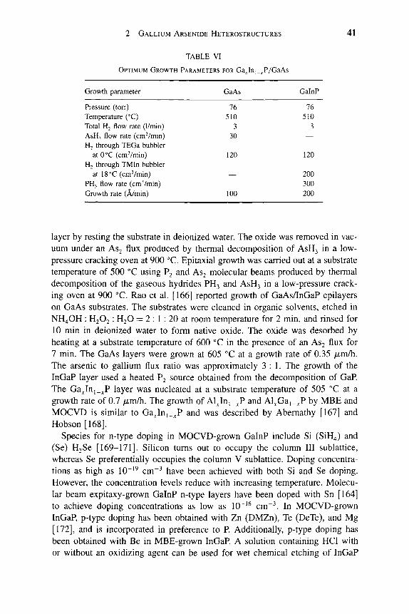
2 GALLIUM ARSENIDE HETEROSTRUCTURES 41
TABLE VI
OPTIMUM GROWTH PARAMETERS FOR Ga^In,_^P/GaAs
Growth parameter
Pressure (torr) Temperature (°C) Total H2 flow rate (1/min) ASH3 flow rate (cmVmin) H2 through TEGa bubbler
atO°C (cmVmin) H2 through TMIn bubbler
at 18°C(cmVmin) PH3 flow rate (cm^/min) Growth rate (A/min)
GaAs
76 510
3 30
120
—
100
GalnP
76 510
3 —
120
200 300 200
layer by resting the substrate in deionized water. The oxide was removed in vac-uum under an AS2 flux produced by thermal decomposition of ASH3 in a low-pressure cracking oven at 900 °C. Epitaxial growth was carried out at a substrate temperature of 500 °C using P2 and AS2 molecular beams produced by thermal decomposition of the gaseous hydrides PH3 and AsHj in a low-pressure crack-ing oven at 900 °C. Rao et al. [166] reported growth of GaAs/InGaP epilayers on GaAs substrates. The substrates were cleaned in organic solvents, etched in NH4OH : H2O2: H2O = 2 : 1 : 20 at room temperature for 2 min, and rinsed for 10 min in deionized water to form native oxide. The oxide was desorbed by heating at a substrate temperature of 600 °C in the presence of an AS2 flux for 7 min. The GaAs layers were grown at 605 °C at a growth rate of 0.35 /xm/h. The arsenic to gallium flux ratio was approximately 3 : 1 . The growth of the InGaP layer used a heated P2 source obtained from the decomposition of GaP. The Ga^Ini_^P layer was nucleated at a substrate temperature of 505 °C at a growth rate of 0.7 fim/h. The growth of Al^Ini_j,P and Al Ga . ^P by MBE and MOCVD is similar to Ga^In^.^P and was described by Abemathy [167] and Hobson [168].
Species for n-type doping in MOCVD-grown GalnP include Si (SiH4) and (Se) H2Se [169-171]. Silicon turns out to occupy the column III sublattice, whereas Se preferentially occupies the column V sublattice. Doping concentra-tions as high as 10"'^ cm~^ have been achieved with both Si and Se doping. However, the concentration levels reduce with increasing temperature. Molecu-lar beam expitaxy-grown GalnP n-type layers have been doped with Sn [164] to achieve doping concentrations as low as 10"^^ cm~^ In MOCVD-grown InGaP, p-type doping has been obtained with Zn (DMZn), Te (DeTe), and Mg [172], and is incorporated in preference to P. Additionally, p-type doping has been obtained with Be in MBE-grown InGaP A solution containing HCl with or without an oxidizing agent can be used for wet chemical etching of InGaP

42 ERIC DONKOR
HCi 12,000
16.000^
1 2 . 0 0 0 / 10,800 \ 3 0 0 0
H3PO4 0 0 0 H2O
FIG. 14. Etch rates of InGaP (in angstroms per minute) at 25 °C in H3PO4/HCI/H2O solutions. Reproduced with permission from S. J. Pearton, "Handbook of Compound Semiconductors" (P. H. Holloway and G. E. McGuire, Eds.), Chap. 8. ©1995 Noyes, Park Ridge, NJ.
[173, 174]. Figure 14 shows the etch rates of InGaP in HCI/H3PO4/H2O mix-tures as a function of the relative ratio of the etchants [151].
The etch rates increase with increasing HCI concentration, but the fastest rate is achieved with the addition of dilute H3PO4 solution. In general, the etch rate of InGaP varies between 1 and 1.2 /im/min in a pure solution of HCI at room temperature [175]. A comparison of dry etching by reactive ion etching and electron cyclotron resonance has been reported.
The crystalline structure of GalnP may be ordered such that sheets of pure Ga, In, and P atoms alternate on the planes of the basic unit cell without intermixing of the Ga and In atoms on the same lattice plane as shown in Figure 15. Trans-mission electron diffraction (TED), transmission electron microscopy. X-ray diffraction, and variations in energy bandgap all have been used to study order-ing. However, these methods can lead to significantly different conditions for ordering. For example, widely different optimal conditions have been reported for ordering in Ga^In^.^P by Kondow et al. [176], Suzuki et al. [172], and Gomyo et al. [177]. Such discrepancies can be attributed to the dependence of image patterns on film thickness, beam profile, and substrate quality.
Growth temperature, growth rate, V : III ratio, substrate quality, substrate ori-entation, and dopants are some of the parameters that influence ordering of atoms in epitaxial layers. The effect of growth temperature on atomic ordering in Ga^Ini_^P was studied by Gomyo et al. [177], Morita et al. [178], Kurtz et al. [179], and Okuda et al. [180]. These studies indicate that, for a fixed V : III ratio and substrate orientation, ordering is maximal in the temperature
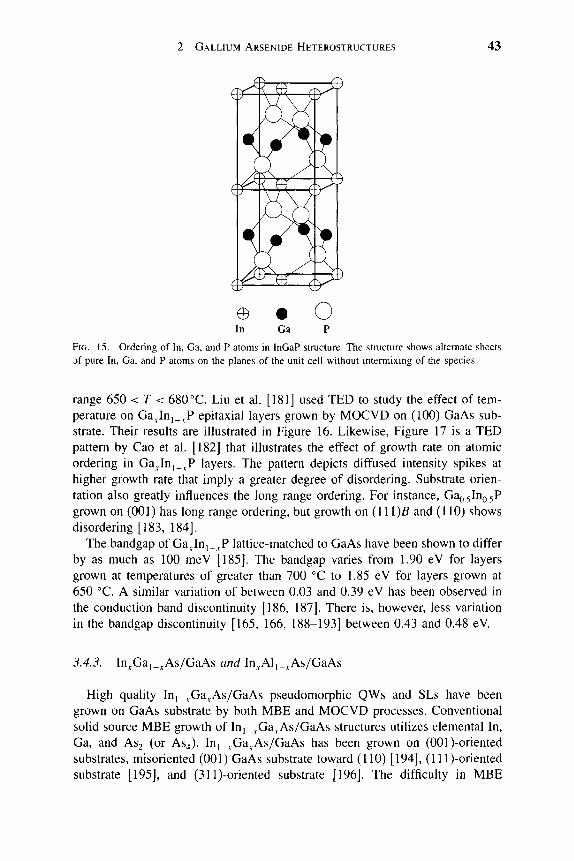
2 GALLIUM ARSENIDE HETEROSTRUCTURES 43
FIG. 15. Ordering of In, Ga, and P atoms in InGaP structure. The structure shows alternate sheets of pure In, Ga, and P atoms on the planes of the unit cell without intermixing of the species.
range 650 < 7 < 680 °C. Liu et al. [181] used TED to study the effect of tem-perature on Ga^Ini_^P epitaxial layers grown by MOCVD on (100) GaAs sub-strate. Their results are illustrated in Figure 16. Likewise, Figure 17 is a TED pattern by Cao et al. [182] that illustrates the effect of growth rate on atomic ordering in Ga^Ini_^P layers. The pattern depicts diffused intensity spikes at higher growth rate that imply a greater degree of disordering. Substrate orien-tation also greatly influences the long range ordering. For instance, Ga()5lno5P grown on (001) has long range ordering, but growth on (111)B and (110) shows disordering [183, 184].
The bandgap of Ga^Ini_^P lattice-matched to GaAs have been shown to differ by as much as 100 meV [185]. The bandgap varies from 1.90 eV for layers grown at temperatures of greater than 700 °C to 1.85 eV for layers grown at 650 °C. A similar variation of between 0.03 and 0.39 eV has been observed in the conduction band discontinuity [186, 187]. There is, however, less variation in the bandgap discontinuity [165, 166, 188-193] between 0.43 and 0.48 eV.
3.4.3. In^Gai_^As/GaAs and In^Al|_^As/GaAs
High quaUty Ini_^Ga_^As/GaAs pseudomorphic QWs and SLs have been grown on GaAs substrate by both MBE and MOCVD processes. Conventional soUd source MBE growth of Ini_^Ga^As/GaAs structures utilizes elemental In, Ga, and As2 (or AS4). Ini_^Ga^As/GaAs has been grown on (OOl)-oriented substrates, misoriented (001) GaAs substrate toward (HO) [194], (lll)-oriented substrate [195], and (311)-oriented substrate [196]. The difficulty in MBE
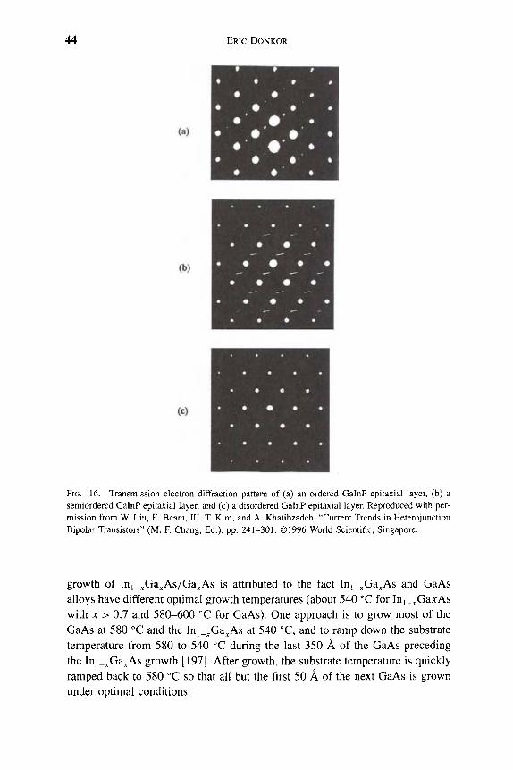
44 ERIC DONKOR
(a)
(b)
(c)
FIG. 16. Transmission electron diffraction pattern of (a) an ordered GalnP epitaxial layer, (b) a semiordered GalnP epitaxial layer, and (c) a disordered GalnP epitaxial layer. Reproduced with per-mission from W. Liu, E. Beam, III, T. Kim, and A. Khatibzadeh, "Current Trends in Heterojunction Bipolar Transistors" (M. F. Chang, Ed.), pp. 241-301. ©1996 World Scientific, Singapore.
growth of Ini_^Ga^As/Ga^As is attributed to the fact Ini_xGa^As and GaAs alloys have different optimal growth temperatures (about 540 °C for In^.^^GaxAs with X > 0.7 and 580-600 °C for GaAs). One approach is to grow most of the GaAs at 580 °C and the In^.^Ga^As at 540 °C, and to ramp down the substrate temperature from 580 to 540 °C during the last 350 A of the GaAs preceding the Ini_^Ga^As growth [197]. After growth, the substrate temperature is quickly ramped back to 580 °C so that all but the first 50 A of the next GaAs is grown under optimal conditions.
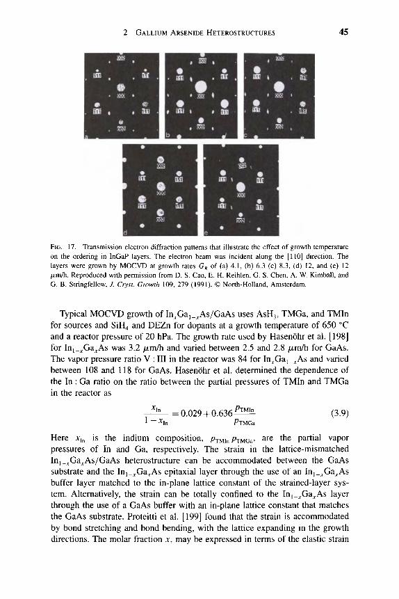
2 GALLIUM ARSENIDE HETEROSTRUCTURES 45
FIG. 17. Transmission electron diffraction patterns that illustrate the effect of growth temperature on the ordering in InGaP layers. The electron beam was incident along the [110] direction. The layers were grown by MOCVD at growth rates G^ of (a) 4.1, (b) 6.3 (c) 8.3, (d) 12, and (e) 12 fim/h. Reproduced with permission from D. S. Cao, E. H. Reihlen, G. S. Chen, A. W. Kimball, and G. B. Stringfellow, J. Cryst. Growth 109, 279 (1991). © North-Holland, Amsterdam.
Typical MOCVD growth of In^Ga^.^As/GaAs uses ASH3, TMGa, and TMIn for sources and SiH4 and DEZn for dopants at a growth temperature of 650 °C and a reactor pressure of 20 hPa. The growth rate used by Hasenohr et al. [198] for lUj.^Ga^As was 3.2 /im/h and varied between 2.5 and 2.8 fxxnih for GaAs. The vapor pressure ratio V : III in the reactor was 84 for In^Ga^.^As and varied between 108 and 118 for GaAs. Hasenohr et al. determined the dependence of the In : Ga ratio on the ratio between the partial pressures of TMIn and TMGa in the reactor as
1 ^ ^ ^ - 0 . 0 2 9 + 0.636^^^^^ (3.9)
Here x^^ is the indium composition, / TMinPxMGa' ^^^ the partial vapor pressures of In and Ga, respectively. The strain in the lattice-mismatched Ini_^Ga^As/GaAs heterostructure can be accommodated between the GaAs substrate and the In^.^Ga^As epitaxial layer through the use of an In^.^Ga^As buffer layer matched to the in-plane lattice constant of the strained-layer sys-tem. Alternatively, the strain can be totally confined to the In^.^Ga^As layer through the use of a GaAs buffer with an in-plane lattice constant that matches the GaAs substrate. Proteitti et al. [199] found that the strain is accommodated by bond stretching and bond bending, with the lattice expanding in the growth directions. The molar fraction jc, may be expressed in terms of the elastic strain

46 ERIC DONKOR
as
^GaAs "inAs C,,+2C, ' '"''' (3.10)
Here C^ and C12 are the elastic stiffness constants of the epilayer material, and ctQaAs ^^^ inAs ^ e the lattice constants for GaAs and InAs, respectively. The strain relaxation processes of the epitaxial mismatched layers give rise to surface fluctuations [200, 201]. Two known types of surface fluctuations are island formation [202, 203] and striations [204].
The dependence of the energy gap of In^Gaj^^As on the JCJ composition is [205]
£^ =0.475(1-Xij2 4-0.6337(1-XiJ + 0.4105 (3.11)
The energies of the conduction and valence band extrema of the Ga^Ini_^As show a linear relationship for the valence band energy and a quadratic function for the conduction band energy. Photoluminescence excitation data appear to indicate that light holes are confined in the GaAs layer, while the heavy holes are confined in the In^Gai__^As layer. This analysis is confirmed by a number of theoretical reports [206-209]. Electron Raman scattering experiments indicate a dependence of the band offset on transition energy [210].
3.5. HETEROSTRUCTURES OF THE TYPE II I -V^-VJ^^/GAAS
3.5.1. GaAsi_,P^/GaAs and GaAs,_^SbJGaAs
The MOCVD growth of GaAsi__^Sb^/GaAs has been reported under atmo-spheric pressure [211, 212]. The most common precursors are TMGa, TMSb, and ASH3. Iwamura et al. [213] used TEGa, TBAs, and TMSb as precur-sors at low pressure on (001) semi-insulating GaAs. The partial pressure of the TEGa was 0.5 Pa, the V : III ratio was between 1 and 7, and the growth temperature was between 475 and 550 °C. Egger et al. [214] have grown both GaAsi__^P^/GaAs and GaAsi_^Sb^/GaAs. The substrate temperature for the GaAsi__,P^/GaAs growth was 650 °C and for the GaAsi_^Sb_,/GaAs was 525 °C. Sources used for the growth of the GaAs substrate were TBAs and TEGa. The ternary alloys GaAsi_^P^ and GaAsi_^Sb^ were grown by the addi-tion of PH3 and TMSb, respectively. The reactor chamber was 50 mbar in the case of GaAsi_^P^/GaAs and 100 mbar for GaAs,_^Sb^/GaAs. The structures were grown on (100) GaAs substrate oriented by 2° toward (110). Composi-tional mixing also has been reported for GaAs,_^P^/GaAs [215-217]. These results indicate that compositional mixing on the anion sublattice has a non-linear dependence on the incident flux ratio. Cunningham et al. [218] fitted a quadratic relation for the anion incorporation of relaxed GaAsi_^P^ layers. The

2 GALLIUM ARSENIDE HETEROSTRUCTURES 47
GaAsi_^Sb^ has a wide miscibility gap, which can induce phase separation. This can lead to compositional mixing if the growth process is away from thermal equilibrium. At a low growth temperature of 420 °C, GaAsi_^Sb^ can be grown over the entire range 0 < jc < 1. At a higher growth temperature, the As content in the alloy increases, and the MOCVD-grown GaAsi_^Sb^ material is uninten-tionally p-type doped. Energy gaps given by Capizzi et al. for GaAsi_^P^ [219] and by Nahory et al. [220] for GaAsi_,Sb^ are
GaAsP = 1.42+1.172x + 0.186x^ 0 < x < l (3.12)
:GaAsSb = 1.42-1.9X+1.2x2 0 < x < 1 (3.13) E,
3.6. HETEROSTRUCTURES OF THE TYPE (III^-IIII_^)^-IIII_^-V/GAAS
(Al^-Gai_^)o5lno5P lattice-matched to GaAs is the most common het-erostructure of this family system and its growth by MOCVD for the entire range 0 < JC < 1 is well established [221-223]. The alloy is typical grown on (001)-oriented GaAs substrate at low pressure. Nozaki et al. [224] used source mate-rials TMIn, TMGa, TMAl, and PH3, and a V : III ratio of 400. Growth occurred at a wide temperature range between 570 and 700 °C. Qingxuan et al. [225] demonstrated growth at atmospheric pressure and a V : III ratio between 50 and 200. The GaAs substrate was misoriented by 2-3° toward (110). Growth rates between 1 and 4 /^m were reported.
The most common n- and p-type dopants are Si and Zn, respectively. The carrier concentration of Si-doped (Al^-Gai_^)osings? increases with increasing mole fraction of dopant, but decreases with increasing V : III ratio. Diluted SiH4 is a common source for n doping. Incidentally, increased concentrations of SiH4 have been known to reduce the Al content of the alloy [226].
(Al^-Gai_^)o5lno5P grown on (001) exhibits a CuPt-type crystal ordering of the group III atoms on the column III sublattice. However, thermal annealing can convert an ordered (Al^-Gai_^)osings? alloy into a disordered structure [227]. Disordering can also occur due to diffusion of heavy atomic species such as Zn and Mg. The room temperature energy gap [228] and electron effective mass [229] as functions of composition x are, respectively, given by
£ = 1.9 + 0.6X (3.14)
m
m. ^ = 0.042+ 0.0328JC (3.15) 0
3.7. HETEROSTRUCTURES OF THE TYPE III^-IIII_^-V^-VI_^,/GAAS
The most important heterostructure in this family is Ga^In,_^As^?i_^/GaAs. It has been grown by both MOCVD [230] and MBE [231]. Zhang et al. [232]

48 ERIC DONKOR
have grown lattice-matched Ga^Ini_^ASyPi_ , on GaAs for the entire compo-sition range 0 <y < I using gas source MBE process. Their sources were In and Ga molecular beams produced from Knudsen effusion cells and As2 and P2 molecular beams produced by thermal decomposition of ASH3 and PH3 in a high-pressure cracker cell at 950 °C. The growth temperature was 583 °C. For MOCVD growth, Ishibashi et al. [233] used TMGa, TMIn, TMAl, ASH3, and PH3 as precursors and (001) GaAs substrate. The growth temperature was 750 °C, under low pressure of 76 torr with a V : III ratio of 350. The p-type dopant was Zn using DEZn as a source. The activation of the Zn acceptors depended strongly on postannealing cooling. The most common n-type dopant is from Si (silane). The energy gap of the Ga^Ini_^As^,Pi_^,/GaAs system is given by [234]
E^ = 1.35+ 0.668JC-1.068^ + 0.758x2+ 0 .07/ ' (3.16)
-0.069JCJ - 0322x^y + 0.03x/
The energy gap of Ga^In^.^^As^Pi.^/GaAs can be tailored to correspond to the wavelength region between 0.6 < A < 1.1 jum [235, 236].
4. Physical Properties of GaAs-Based Quantum Well Structures and Superlattices
4.1. INTRODUCTION
Consider a heterostructure formed from alternating layers of semiconductors A and B, where the constituents A and B may be elemental or /i-ary compound alloys. Let the energy gap of A be larger than the energy gap of B (E^^ > E^^). Three basic band alignments can arise from a heterostructure formed from differ-ent types of A and B: (1) type I or straddling alignment, (2) type II or staggered alignment, and (3) type III or broken gap alignment. These different configu-rations are depicted in Figure 18. Figure 18a illustrates a type I (straddling) configuration formed at the hetrointerface of IUQ53Gao47As {E^^ = 0.75 eV) and Ino52Gao48As (^^^ = 1.44 eV). The structure has conduction and valence band offsets of opposite sign (A£^ = 0.47 eV and AE^ = —0.22 eV, respec-tively). In the type I configuration, the electrons and holes are both confined within the same layer. A type II (staggered) configuration is formed between AlSb (Eg^ = 1.58 eV) and InAs (E^^ = 0.36 eV) as shown in Figure 18b. In contrast to type I, we notice here that the valence band of the smaller bandgap material lies below that of the larger bandgap material, so that the band offsets have the same sign (AE^ = 1.35 eV and AE^ = 0.13 eV). In the type III (broken gap) configuration shown in Figure 18c, the magnitude of the offset is so large between InAs and GaSb that the forbidden gap no longer overlaps. However,

2 GALLIUM ARSENIDE HETEROSTRUCTURES 49
ino.53Gao.47As ino.52Alo.48As
i^ AEv
AEc=0.47eV, AEv=0.22eV
a) Type-I or straddling
InAs AlSb
A
AEc f r EgA=1.58eV
EgB=0.36eV
AEv
AEc=1.35eV,AEv=-0.13eV
b) Type-II or staggered
InAs GaSb
AEc
T t EgB=0.36eV
i
J i
J ^
EgA=0.73 eV
r i
^ AEv
AEc=0.88eV,AEv=-0.51eV
c) Type-Ill or broken gap
FIG. 18. (a) Type I (straddling) configuration formed at the hetrointerface of Ino53Gao47As (Eg^ = 0.75 eV) and Ing 5263048As (E^j^ = 1.44 eV). The structure has conduction and valence band off-sets of opposite sign {AE^ = 0.47 eV and A£ , = -0.22 eV, respectively), (b) Type II (staggered) configuration formed between AlSb {E^j^ = 1.58 eV) and InAs {E^^ = 0.36 eV), where the valence band of the smaller bandgap material lies below that of the larger bandgap material, so that the band offsets have the same sign (AE^ = 1.35 eV and AE^, =0.13 eV). (c) Type III (broken gap) config-uration between InAs and GaSb. The magnitude of the offset is so large that the forbidden gap no longer overlaps. However, the band offsets have the same sign {AE^ = 0.88 eV and AE^ = 0.51 eV).

50 ERIC DONKOR
the band offsets have the same sign (Af" = 0.88 eV and A£ , = 0.51 eV). In the type III configuration, the electrons and holes are confined to different layers.
4.2. QUANTUM WELLS ENERGY LEVELS
Figure 11 shows a type I QW structure composed of AlGaAs/GaAs/AlGaAs. The figure shows discrete energy levels due to the confinement of electrons in the conduction band and holes in the valence bands. The figure shows the conduction (E^,, £^2)' hght-hole (£,1, £",,), and heavy-hole (£"^1, £" 2) subbands. The size of the confining barriers or band-edge offsets AE^ and ^E^, determin-ing the effectiveness of the wells to confine the carriers.
There are a number of techniques that have been successfully utilized to calculate the QW energy levels. They most common are (a) the tight-binding approximation [237, 238], (b) the effective-mass or pseudopotential method [239, 240], and (c) the envelope-function approximation [241, 242]. In the tight-binding approximation, one begins with a series of energies, which are characteristics of the sp^ bonds linking one atom to its neighbors. The het-erostructure wave function is then built atom after atom. In the pseudopotential method, staking of the constituents is considered as a perturbation over a zero-order situation, which corresponds to the bulk of one of the constituents. The method is analogous to deep level calculation in bulk semiconductor materials.
The tight-binding approximation and the pseudopotential method are essen-tially microscopic methods. These two techniques give accurate calculations of heterostructure energy levels and are able to reproduce the whole dispersion relation. These two calculations often require intensive computer computation and do not easily provide tractable information about the dispersion relation.
The envelope-function approximation is restricted to calculating the disper-sion relation only at high-symmetry points in the Brillouin zone of the host material. Its advantages include simplicity and closed-form analytically tractable solutions. The key tenets of the envelope-function approximation are described and used to determine the wave functions and subbands for QW, MQW, and SL structures.
4.2.1. Conduction Bands in Quantum Wells
The energy levels of electrons in the conduction band can be calculated using the envelope-function approximation along with the Kane model to describe the electronic states of the host A and B materials. The approximation assumes (1) an interface potential that is strongly localized at the interfaces between the A and B materials, (2) that the interface potential does not mix the band-edge wave functions but only shifts them, and (3) perfect lattice match between the A and B materials, which also crystallizes with the same crystallographic structure.

2 GALLIUM ARSENIDE HETEROSTRUCTURES 51
The generalized electronic wave function thus consists of two components: the fast varying Bloch function, w j , and the slowly varying envelope function, X. The two components are normalized such that
{X\X)= f X*XdS=l {u\u) = ^ [ . u*udV^l (4.1) Js V " unit cell
where S is the sample area and V^ is the volume of a single unit cell. Inside each layer the wave function is expanded on the periodic parts of the Bloch functions. This gives the electronic wave functions for the edges of the A and B layers, respectively.
.A = Eexp[ / (k r r ) ]<A'„ (4.2)
n
n
where the growth direction is assumed to be in the z direction and k^ is the transverse electron wave vector. The periodic parts of the Bloch functions are also assumed to be the same in each kind of layer that constitutes the QW; therefore, w ^ = wf . The summation index, /i, runs over as many edges as might be included in the analysis. Since the conduction band is nondegenerate, the envelope wave function satisfies Schrodinger's equation
{H, + V)x„ = E,„x„ (4.4)
where the Hamiltonian operator for the conduction band is
' 2 < 2m:, ^ . > .^
Here the index i = w,b stands for the well and barrier regions, respectively. The Schrodinger equation then becomes
( ^ 2 ^2 ^2^2 h^k^\
-2<:^+^^'-+2<;+i^h^^=^-^"(^^ ^'-'^ That is.
m^ if z corresponds to the well layer
m^ if z corresponds to the barrier layer
K. = 0 if z corresponds to the well layer
VQ if z corresponds to the barrier layer
(4.7)
(4.8)

52 ERIC DONKOR
where V^ is the conduction band offset. The solution to Eq. (4.6) with (4.7) and (4.8) is given as
ATeven = AC0S{k^z)\z\ <
= BQxp
= Bexp
hHl hH).
h>l hi
A'odd = Asin{k^z) | z | < -
= Bexp
= Bcxp
hH) H-l)]
] i^i>f H > f
(4.9)
(4.10)
where
Pl^^-^iK-EJ V„<E^<0 kt^ 2m„ fi2
(4.11)
The constants A and B can be determined by matching x ^^^ {^/^i){dx/dz) across each well-barrier interface. For the solution to Eq. (4.9) these conditions yield
A cos
m-ruu \ 2 / niu
Divide (IV. 12b) by (IV. 12a) to get
An,,, V 2 rriu
Similarly, Eq. (IV. 10) gives
ni,,, \ 2
The number of states bound by the well 2iik^ = ky = ^ is given by
A = l+In t
(4.12a)
(4.12b)
(4.13)
(4.14)
(4.15)

2 GALLIUM ARSENIDE HETEROSTRUCTURES 53
4.2.2. Valence Bands in Quantum Wells
The simplicity of the conduction band structure in QWs relies on the fact that the conduction bands are nondegenerate and the interaction with other energy bands is weak. As a result of this weak interaction, the perturbation method can be used to describe the dynamics of the conduction band in terms of an effective mass approximation, which signifies the weak interactions of the con-duction band. If the bands were degenerate, weak interactions could no longer be assumed and, therefore, the effective mass approximation would have to be modified. One such modification is owing to Luttinger and Kohn [243, 244]. Their approach is to modify the effective mass approximation to the one elec-tron Schrodinger equation for each degenerate band by incorporating additional terms to account for coupling between the degenerate bands as well as spin degeneracy.
Depending on the effective coupling between the degenerate bands and spin at the band edge, there can be either two, four, six, or eight coupled differ-ential equations obtained from the modified effective-mass approximation of the Schrodinger equation. Four sets of coupled effective mass equations result if coupUng is between only two bands, say the heavy hole (HH) and light hole (LH). Six coupled effective mass equations result for three band coupling between the HH, LH, and spin-orbit (SO) bands. Eight sets of equations result if there is coupling between the three valence bands (HH, LH, SO) and the conduction band. A four band model that leads to eight effective mass equa-tions has been analyzed [245-247]. However, interaction between the HH and LH bands is by far the strongest and, to a good approximation, the other inter-actions may be neglected. Only when we consider energy levels deep into the valence band (energies comparable to the spin-orbit splitting energy A) do we need to include the SO band in the interactions.
The four coupled effective-mass equations that arise from interactions between the HH and LH bands can be greatly simplified using a modified k • p representation of the energy bands [248-250]. The approach is to define a new set of Bloch functions for the HH and LH (<^hh'^hh'^ih'^ih) bands formed from a Hnear combination of the four Bloch functions for the HH and LH ("hh'^hh' "ih''^ih) equations. The new set of Bloch functions is given by [249]
^hh = "7^(^"hh - «*«hh) (4-16)
^hh = - F ( « « h h - « * " h h ) (4.17)
(Pih = ^( i8i i ih- iS*WHh) (4.18)
^ , , = -^ ( i8 i i ih - i8*"hh) (4.19)

54 ERIC DONKOR
a = —= exp V2
^ = - e x p
/3TT 3d\'
'(-4+2)]
(4.20)
(4.21)
where 6 = tan \ky/kj. The Hamiltonian for the new basis set can be written in matrix form as
(4.22)
^ 1 ,
//|*2
7/1*3
0
H^2
H22
0
^ . 3
Hn 0
H22
- / / | 2
0
H^ -H
W,
H
The matrix in Eq. (IV.22) can be block-diagonaUzed as
H ' - l ^ ' 0 " - | 0 z/'-
where the upper and lower blocks are given by
H''^
+ Q R*
-Q R*
R
P-Q
R P + Q
R^\T\-i\S\
Iina , ;,2 , ,,2 2
2
-^/3
P-^ikl+kl + kl)
Q^Jl{-2kl + kl + kl)
V3 + -^(r3-72)(^.v + ' M
S = V3y^L{k,-ik,)
(4.23)
(4.24a)
(4.24b)
(4.24c)
(4.24d)
(4.24e)
(4.24f)
(4.24g)
where yi, 72' Js ^^e the Luttinger parameters. The unitary transformation, U, which forms a block-diagonahzation of the Hamiltonian, // , into H' = UHU*

2 GALLIUM ARSENIDE HETEROSTRUCTURES 55
is given by
(/ =
V2 exp(—/n)
0
0
0 0
— exp(-/i7) - - - e x p ( / i 7 )
-^exp( - / i7 ) —=exp(/i7) V2 V2
- -y^exp( / a )
0
0
I ^ e x p ( - / a ) 0 0 - p exp(/a)
(4.25)
where H and 17 are to be chosen. The eigenvalues for the Hamiltonian, H', are
E-V = F±{Q!--^rKfl^ (4.26)
where the positive sign is for the heavy holes and the negative sign is for the light holes; that is,
^C\klk] + k]k\^k^Jil)\ 1/2
1/2
(4.27)
(4.28)
References
1. H. Kroemer, Proc. IEEE 51, 1782 (1963). 2. B. L. Sharma and R. K. Purohit, "Semiconductor Heterojuctions." Pergamon, Oxford, 1974. 3. A. G. Milnes and D. L. Feucht, "Heterojunction and Metal Semiconductor Junctions." Aca-
demic Press, New York, 1972. 4. H. Kressel and J. K. Butler, "Semiconductor Lasers and Heterojuction LEDs." Academic
Press, New York, 1977. 5. L. Esaki and R. Tsu, IBM J. Res. Dev. 14, 61 (1970). 6. L. L. Chang, L. Esaki, and R. Tsu, Appl Phys. Lett. 24, 495 (1974). 7. R. Tsu and L. Esaki, Appl. Phys. Lett. 22, 562 (1973). 8. T. Mimura, S. Hiyamizi, T. Fujii, and K. Nanbu, Jpn. J. Appl. Phys. 19, L225 (1980). 9. D. Delagebeaudeuf, P. Delescluse, P. Etienne, M. Laviron, J. Chaplart, and N. T. Linh, Elec-
tron. Lett. 16, 667 (1980). 10. R M. Solomon and H. Morkoc, IEEE Trans. Electron. Devices 31, 1015 (1984). 11. H. Kroemer, Proc. IRE 45, 1535 (1957). 12. H. Kroemer, Proc. IEEE 70, 13 (1982). 13. J. I. Song, K. B. Chough, C. J. Palmstrom, B. R Van der Gaag, and W. R Hong, "IEEE Device
Research Conference," 1994, paper IVB-5.

56 ERIC DONKOR
14. W. T. Tsang, in "Semiconductors and Semimetals" (R. Dingle, Ed.), Vol. 24, Chap. 7. Aca-demic Press, New York, 1987.
15. P. S. Zory, Ed., "Quantum Well Lasers." Academic Press, New York, 1993. 16. F. T. Vasko and A. V. Kuznetsov, "Electronic States and Optical Transitions" in Semiconductor
Heterostnictures," Springer-Verlag, New York, 1999. 17. V. I. Korol'kov, in "Semiconductor Optoelectronics," (M. A. Herman, Ed.), Chap. 14. Wiley,
New York, 1978. 18. D. A. B. Miller, D. S. Chemla, T. C. Damen, T. H. Wood, C. A. Burrus, A. C. Gossard, and
W. Wiegmann, IEEE J. Quantum Electron. 21, 1462 (1985). 19. S. Schmitt-Rink, D. S. Chemla, and D. A. B. Miller, Adv. Phys. 38, 89 (1989). 20. W. Franz, Z. Naturforsch 13a, 484 (1958). 21. L. V. Keldysh, Sov. Phys. JETP 7, 788 (1958). 22. H. M. Manasevit, Appl. Phys. Lett. 12, 156 (1968). 23. H. M. Manasevit, J. Cryst. Growth 55, 1 (1981). 24. G. B. Stringfellow, in "Semiconductors and Semimetals" (R. K. Willardson and A. K. Beer,
Eds.), Vol. 22, pp. 209-259. Academic Press, New York, 1985. 25. G. B. Stringfellow, "Organometallic Vapor-Phase Epitaxy: Theory and Practice." Academic
Press, New York, 1989. 26. T. R Kuech, Mater Sci. Rep. 2(1), 1 (1987). 27. R M. Frijlink, J. Cryst. Growth 93, 292 (1988). 28. M. Behet, A. Brauers, and P Balk, J. Cryst. Growth 107, 209 (1991). 29. P D. Dapkus, B. Y Maa, Q. Chen, W. G. Jeon, and S. P Den Baars, / Cryst. Growth 107,
73 (1991). 30. J. P. Hirtz, M. Razeghi, M. Bonnet, and J. P. Duchemin, in "GalnAsP Alloy Semiconductors"
(T. P Pearsall, Ed.). Wiley, New York, 1982. 31. K. Ploog, in "Springer Proceedings in Physics" (G. LeLay, J. Derrien, and N. Boccara, Eds.),
Vol. 22, p. 10. Springer-Veriag, New York, 1987. 32. T. J. Drummond, H. Morkoc, and A. Y Cho, J. Cryst. Growth 56, 449 (1982). 33. G. E. Stillman, S. S. Bose, M. H. Kim, B. Lee, and T. S. Low, in "Handbook on Semicon-
ductors" (S. Mahajan, Ed.), Vol. 3a, Chap. 10. North-Holland, Amsterdam, 1992. 34. S. Amelinckx, in "Supplement to Solid State Physics" (F. Seitz and D. Tumbull, Eds.), Vol. 6,
p. 15. Academic Press, New York, 1964. 35. K. Sangwal, "Etching of Crystals," North-Holland, Amsterdam, 1987. 36. P. H. L. Notten, J. E. A. M. vanden Meerakker, and J. J. Kelly, "Etching of II-V Semicon-
ductors: An Electrochemical Approach." Elsevier, Oxford, 1991. 37. J. L. Weyher, in "Handbook on Semiconductors" (S. Mahajan, Ed.), Vol. 3a, Chap. 11. North-
Holland, New York, 1994. 38. K. F Jensen, J. Cryst. Growth 107, 1 (1991). 39. M. Razeghi, in "Handbook on Semiconductors" (S. Mahajan, Ed.), Vol. 3a. North-Holland,
New York, 1994. 40. G. A. Hebner, K. P Kileen, and R. M. Biefeld, / Cryst. Growth 98, 293 (1989). 41. D. K. Gaskill V. Kolubeyev, N. Bottka, R. S. Sillmon, and J. E. Butler, J. Cryst. Growth 93,
1 (1988). 42. C. A. Larsen, N. L Buchan, and G. B. Stringfellow, Appl. Phys. Lett. 52, 480 (1988). 43. T. F. Kuech, E. Veuhoff, T. S. Kuan, V. Deline, and R. Potemski, J. Cryst. Growth 11, 257
(1986). 44. N. Kobayashi and T. Makimoto, Jpn. J. Appl. Phys. 24, L824 (1985). 45. P Rai-Chaudhury, J. Electrochem. Soc. 116, 1745 (1969). 46. T. F Kuech, M. A. Tischler, P J. Wang, G. Scilla, R. Potemski, and F Cardone, Appl. Phys.
Lett. 53, 1317 (1988). 47. A. Y Cho and J. R. Arthur, in "Progress in Solid State Chemistry" (G. Somojai and J.
McCaldin, Eds.), Vol. 10, Chap. 3, pp. 157-191. Pergamon, New York, 1975.

2 GALLIUM ARSENIDE HETEROSTRUCTURES 57
48. L. L. Chang and R. Ludeke, in "Epitaxial Growth" (J. W. Matthews, Ed.), Part A, Chap. 2, pp. 37-72. Academic Press, New York, 1975.
49. J. R. Arthur, Surf. Sci. 43, 449 (1974). 50. C. T. Foxon and B. A. Joyce, Surf. Sci. 64, 293 (1977). 51. D. K. Biegelsen, R. D. Bringans, J. E. Northrup, and L. E. Swartz, Phys. Rev. B 41, 5701
(1990). 52. I. Kamiya, D. E. Aspnes, H. Tanaka, L. F. Florez, M. A. Koza, R. Bhat, and J. P Harbison,
in "Semiconductor Growth, Surfaces and Interfaces" (G. J. Davies and R. H. Williams, Eds.), Chap. 1. Chapman and Hall, New York, 1994.
53. A. G. Milnes, in "Advances in Electronics and Electron Physics" (P. W. Hawkes, Ed.), pp. 64-161. Academic Press, New York, 1983.
54. G. M. Martin and S. Makram-Ebeid, in "Deep Centers in Semiconductors," 2nd ed. (S. T. Pantelides, Ed.), Chap. 6. Gordon and Breach, Philadelphia, 1992.
55. M. Ilegems, J. Appl. Phys. 48, 1278 (1977). 56. K. Ploog, A. Fischer, and H. Kunzel, J. Electrochem. Soc. 128, 400 (1981). 57. N. Duhamel, P Henoc, F Alexandre, and E. V. K. Rao, Appl. Phys. Lett. 39, 49 (1981). 58. D. L. Miller and P M. Asbeck, J. Appl Phys. 57, 1816 (1985). 59. Y C. Pao, T. Hierl, and T. Cooper, J. Appl. Phys. 60, 201 (1986). 60. J. L. Lievin and F Alexandre, Electron. Lett. 21, 413 (1985). 61. A. Y Cho and I. Hayashi, J. Appl. Phys. 42, 4422 (1971). 62. C. E. C. Wood, J. Woodcook, and J. J. Harris, Inst. Phys. Conf. Ser 45, 28 (1979). 63. J. S. Blakemore, "Gallium Arsenide," Vol. 1, Chap. 1. American Institute of Physics,
New York, 1987. 64. O. Madelung, "Data in Science and Technology: Semiconductors," p. 104. Springer-Verlag,
New York, 1991. 65. S. Ida and K. Ito, J. Electrochem. Soc. 118, 768 (1971). 66. W. Kern, RCA Rev. 39, 278 (1978). 67. J. de Launay, in "Solid State Physics" (F Seitz and D. Tumbull, Eds.), Vol. 2, p. 219. Aca-
demic Press, New York, 1956. 68. Data in science and technology: Semiconductor Group IV Elements and III-V compounds,
Ed, O. Mandelung, pp. 104, Springer-Verlag, New York, 1991. 69. J. R. Chelikowsky and M. L. Cohen, Phys. Rev. B 14, 555 (1976). 70. C. Hermann and C. Weisbuch, Phys. Rev. B 15, 823 (1977). 71. D. L. Rode, in "Semiconductors and Semimetals" (R. K. Willardson and A. C. Beer, Eds.),
pp. 1-89. Academic Press, New York, 1975. 72. J. H. Marsh, P. A. Houston, and P. N. Robson, "Gallium Arsenide and Related Compounds,"
Institute of Physics, Bristol, 1981. 73. H. Ehrenreich, J. Phys. Chem. Solids 8, 130 (1959). 74. A. Fortini, D. Diguet, and J. Lugand, J. Appl. Phys. 41, 3121 (1970). 75. J. R. Hayes, A. R. Adams, and P. D. Greene, in "Low-Field Carrier Mobility in GalnAsP" (T.
P Pearsall, Ed.), Chap. 8. Wiley, New York, 1982. 76. F. C. Frank and J. H. van der Merwe, Proc. R. Soc. London, Ser A 198, 216 (1949). 77. J. H. van der Merwe, Crit. Rev. Solid State Mater Sci. 7, 209 (1978). 78. Y H. Lo, Appl. Phys. Lett. 59, 2311 (1996). 79. C. Carter-Coman, R. Bicknell-Tassius, A. S. Brown, and N. M. Jokerst, Appl. Phys. Lett. 70,
1754 (1997). 80. L. B. Freund and W. D. Nix, Appl. Phys. Lett. 69, 173 (1996). 81. D. L. Smith and C. Mailhiot, Rev. Mod Phys. 62, 173 (1990). 82. K. B. Laurich, K. Elcess, C. G. Fonstad, J. G. Beery, C. Mailhiot, and D. L. Smith, Phys.
Rev. Lett. 62, 649 (1989). 83. B. S. Yoo, B. D. McCombe, and W Schaff, Phys. Rev. B 44, 13,152 (1991).

58 ERIC DONKOR
84. U. D. Venkateswaran, T. Burnett, L. J. Cui, M. Li, B. Weinstein, H. M. Kim, C. R. Wie, K. Elcess, C. G. Fostand, and C. Mailhiot, Phys. Rev. B 42, 3100 (1990).
85. J. W. Matthews and A. E. Blakeslee, J. Cryst. Growth 27, 118 (1974). 86. R. People and J. C. Bean, Appl Phys. Lett. 47, 322 (1985). 87. W. A. Jesser and D. Kuhlmann-Wilsdorf, Phys. Status Solidi 19, 95 (1967). 88. J. R Hirth and J. Lothe, "Theory of Dislocation." Wiley, New York, 1982. 89. A. Zunger and S. Mahajan, in "Handbook on Semiconductors" (S. Mahajan, Ed.), Vol. 3b,
p. 1403. North-Holland, New York, 1992. 90. M. B. Derbali, J. Meddeb, H. Maaref, D. Buttard, R Abraham, and Y Monteil, J. Appl. Phys.
84, 503 (1998). 91. T. Kimura, T. Kimura, E. Ishimura, F. Uesugi, M. Tsugami, K. Mizuguchi, and T. Murotani,
J. Cryst. Growth 107, 827 (1991). 92. D. J. Olego, Y Okuno, T. Kawano, and M. Tamura, / Appl. Phys. 71, 4492 (1992). 93. S. J. J. Teng, J. M. Ballingal, and R J. Rosenbaum, Appl. Phys. Lett. 48, 1217 (1986). 94. M. K. Lee, D. S. Wuu, and H. H. Tung, J. Appl. Phys. 62, 3209 (1987). 95. A. Yoshikawa, T. Sugino, A. Nakamura, G. Kano, and I. Teramoto, J. Cryst. Growth 93, 532
(1988). 96. J. W. Matthews, Ed., "Epitaxial Growth," Part B, p. 560. Academic Press, New York, 1975. 97. R. Hull and J. C. Bean, in "Semiconductors and Semimetals" (T. Pearsall, Ed.), Vol. 33, p. 1.
Academic Press, San Diego, 1991. 98. R. M. Graham, A. C. Jones, N. J. Mason, S. Rushworth, L. Smith, and R J. Walker, / Cryst.
Growth 145, 363 (1994). 99. T. F Keuch and E. Veuhoff, J. Cryst. Growth 68, 148 (1984).
100. C. H. Chen, C. T. Chiu, L. C. Su, K. T Huang, J. Shin, and G. B. Stringfellow, J. Electron. Mater 22, 87 (1993).
101. C. H. Chen, Z. M. Fang, G. B. Stringfellow, and R. W. Gedridge, Jr., J. Appl. Phys. 69, 7605 (1991).
102. J. Shin, A. Verma, G. B. Stringfellow, and R. W. Gedridge, Jr., / Cryst. Growth 151, 1 (1995). 103. H. Asahi, X. F. Liu, K. Inoue, D. Marx, K. Asami, K. Miki, and S. Gonda, J. Cryst. Growth
145, 668 (1994). 104. M. Ichimura, K. Higuchi, Y. Hattori, and T Wada, J. Appl. Phys. 68, 6153 (1990). 105. M. Razeghi, in "Handbook on Semiconductors" (S. Mahajan, Ed,), Vol. 3b, Chap. 3. North-
Holland, Amsterdam, 1994. 106. L. M. Fraas, R S. McLeod, R. E. Weiss, L. D. Partian, and J. Cape, J. Appl. Phys. 62, 299
(1987). 107. M. Razeghi, M. Defour, F Omnes, M. Dobers, J. P. Vieren, and Y Guldner, Appl. Phys. Lett.
55, 457 (1989). 108. A. Brauers, M. Weyers, and R Balk, Chemtronics 4, 8 (1989). 109. G. Haacke, S. R Watkins, and H. Bumhard, Appl. Phys. Lett. 54, 2009 (1989). 110. C. H. Chen, C. A. Larsen, and G. B. Stringfellow, Appl. Phys. Lett. 50, 218 (1987). 111. R. H. Lum, J. K. Kingert, and M. G. Lamon, Appl. Phys. Lett. 50, 284 (1987). 112. C. H. Chen, E. H. Reihlen, and G. B. Stringfellow, J. Cryst. Growth 96, 497 (1989). 113. R. Bath, M. A. Koza, and B. J. Skromme, Appl. Phys. Lett. 14, 1386 (1987). 114. T. Fukunaga, T. Takamori, and H. Nakashima, / Cryst. Growth 81, 85 (1987). 115. W. L Wang, Surf. Sci. 174, 31 (1986). 116. S. Subbanna, H. Kroemer, and J. L. Merz, J. Appl. Phys. 59, 488 (1986). 117. A. Y Cho, J. Appl. Phys. 41, 2780 (1970). 118. R. H. Walhs, M. A. D. Forte-Poisson, M. Bonnet, G. Beuchet, and J. P Duchemin, Inst. Phys.
Conf. Ser 56, 73 (1981). 119. H. Terao and H. Sunakawa, J. Cryst. Growth 68, 157 (1984). 120. M. Hata, N. Fukuhara, Y Zempo, M. Isemura, T. Yako, and T. Maeda, J. Cryst. Growth 93,
543 (1988).

2 GALLIUM ARSENIDE HETEROSTRUCTURES 59
121. M. S. Goorsky, T. F. Kuech, F. Cardone, P. M. Mooney, G. J. Scilla, and R. M. Potemski, Appl. Phys. Lett. 58, 1979 (1991).
122. C. R. Abemathy, A. S. Jordan, S. J. Pearton, W. S. Hobson, D. A. Bohling, and G. T. Muhr, Appl. Phys. Lett. 56, 2654 (1990).
123. H. C. Casey, Jr., A. Y. Cho, D. V. Lang, E. H. Nicollian, and P W. Foy, J. Appl. Phys. 50, 3484 (1979).
124. H. Morkoc, A. Y. Cho, and C. Radice, J. Appl. Phys. 51, 4882 (1980). 125. J. P. Andre, C. Schiller, A. Mitonneau, A. Bnere, and J. Y. Aupied, Inst. Phys. Conf. Sen 65,
117(1983). 126. C. T. Foxon, J. B. Clegg, K. Woodbridge, D. Hilton, P Dawson, and P Blood, J. Vac. Sci.
TechnoL, B 3, 703 (1985). 127. K. Akimoto, M. Kamada, K. Taira, M. Aral, and N. Watanabe, / Appl. Phys. 59, 2833 (1986). 128. C. Amano, K. Ando, and M. Yamaguchi, J. Appl. Phys. 63, 2853 (1988). 129. M. Meuris, W. Vandervorst, and G Borghs, J. Vac. Sci. TechnoL, A 7, 1663 (1989). 130. T. Achtnich, G Burri, and M. Ilegems, J. Vac. Sci. TechnoL, A 7, 2532 (1989). 131. D. W. Kisker, J. N. Miller, and G B. Stringfellow, J. AppL Phys. Lett. 40, 614 (1982). 132. P D. Kirchner, J. M. Woodall, J. L. Freeouf, and G D. Pettit, AppL Phys. Lett. 38, 427 (1981). 133. K. A. Prior, G J. Davies, and R. Heckingbottom, J. Cryst. Growth 66, 55 (1984). 134. K. Tamamura, J. Ogawa, K. Akimoto, Y Mori, and C. Kojima, AppL Phys. Lett. 50, 1149
(1987). 135. T. Hayakawa, M. Kondo, T. Suyama, K. Takahashi, S. Yamamoto, and T. Hijikata, AppL Phys.
Lett. 52, 339 (1988). 136. J. P. de Souza and D. K. Sadana in "Handbook on Semiconductors" (S. Mahajan, Ed.), Vol. 3b,
Chap. 27. North-Holland, Amsterdam, 1994. 137. S. K. Tiku and W. M. Duncan, J. Electrochem. Soc. 123, 2237 (1985). 138. R. Zolch, H. Ryssel, H. Kranz, H. Reichel, and I. Ruge, in "Ion Implantation in Semiconduc-
tors" (F. Chemow, J. A. Borders, and D. K. Brice, Eds.), p. 595. Plenum, New York, 1976. 139. D. E. Davies and P J. McNally, IEEE Electron Device Lett. EDL-4, 356 (1983). 140. K. Tabatabaie-Alavi and I. W. Smith, IEEE Trans. Electron Devices 37, 96 (1990). 141. R. T. Blunt, R. Szweda, M. S. M. Lamb, and A. G Cullis, Electron. Lett. 20, 444 (1984). 142. M. Skowronski, in "Handbook on Semiconductors" (S. Mahajan, Ed.), Vol. 3b, Chap. 18.
North-Holland, Amsterdam, 1994. 143. Y Mori and N. Watanabe, / Electrochem. Soc. 125, 1510 (1978). 144. J. L. Merz and R. A. Logan, J. AppL Phys. 47, 3503 (1976). 145. P K. Chatterjee and G B. Larrabee, IEEE Trans. VLSI Syst. 1, 7 (1993). 146. S. K. Ghandhi, "VLSI Fabrication Principles, Silicon and Gallium Arsenide," pp. 475-532.
Wiley Interscience, New York, 1983. 147. S. Adachi and K. Oe, J. Electrochem. Soc. 130, 2427 (1983). 148. D. N. MacFadyen, J. Electrochem. Soc. 130, 1934 (1983). 149. D. W Shaw, J. Electrochem. Soc. 128, 874 (1981). 150. M. Otsubo, T. Oda, H. Kurmale, and H. Miki, J. Electrochem. Soc. 123, 576 (1976). 151. S. J. Pearton, in "Handbook of Compound Semiconductors" (P. H. Holloway and G E.
McGuire, Eds.), Chap. 8. Noyes Park Ridge, NJ, 1995. 152. D. W. Shaw, J. Electrochem. Soc. 113, 958 (1966). 153. C. M. Melliar-Smith and C. J. Mogab, in "Thin Film Processes" (J. L. Vossen and W. Kerns,
Eds.), p. 497. Academic Press, New York, 1978. 154. R. F. Kazarinov and R. A. Suris, Sov. Phys. Semicond. 7, 347 (1973). 155. B. D. McCombe and A. Petron in "Handbook on Semiconductors," Vol. 2, (M. Balkanski,
Ed.), Chap. 6, North-Holland, 1994. 156. C. Weisbuch, "Semiconductor and Semimetals," Vol 24 (R. Dingle, Ed.), Chap. 1, Academic,
New York.

60 ERIC DONKOR
157. D. S. Chelma, D. A. B. Miller, P. W. Smith, A. C. Gossard, and W. Wiegmann, IEEE J. Quantum Electron. QE-20, 265 (1984).
158. C. Weisbuch, R. C. Miller, R. Dingle, A. C. Gossard, and W. Wiegmann, Solid State Commun. 37, 219 (1981).
159. J. C. Mann, in "Physics and Applications of Quantum Wells and Superlattices" (E. E. Mendez and K. von Klitzing, Eds.), p. 347. Plenum, New York, 1987.
160. J. Yoshino, T. Iwamoto, and H. Kukimoto, J. Cryst. Growth 55, 74 (1981). 161. I. Hino and T. Suzuki, / Cryst. Growth 68, 483 (1984). 162. M. Razeghi, M. Defour, and R Omnes, Appl. Phys. Lett. 55, 457 (1989). 163. C. C. Hsu, R. M. Cohen, and G. B. Stringfellow, J. Cryst. Growth 62, 648 (1983). 164. P Blood, J. S. Roberts, and J. P Stagg, J. Appl. Phys. 53, 3145 (1982). 165. M. J. Hafich, J. H. Quigley, R. E. Owens, G. Y. Robinson, and D. L. Otsuka, Appl. Phys. Lett.
54, 2686 (1989). 166. M. A. Rao, E. J. Caine, H. Kroemer, S. I. Long, and D. I. Babic, / Appl. Phy 61, 643 (1986). 167. C. R. Arbemathy, J. Vac. Sci. Technol, A 11, 869 (1993). 168. W S. Hobson, "Proceedings of the Seminar on Wide Bandgap Semiconductor and Devices."
Electrochemical Society Proceedings Vol. 95-21, pp. 26-42, Electrochemical Society, Pen-nington, NJ, 1995.
169. T. Iwamoto, K. Mori, M. Mizuta, and H. Kukimoto, / Cryst. Growth 68, 483 (1984). 170. J. Penndorf, G. Kuhn, H. Neumann, and A. MuUer, Krist. Tech. 15, 169 (1980). 171. Akiku Gomyo, Hitoshi Hotta, Isao Hino, Seiji Kawata, Kenichi Kobayashi and Tohru Suzuki,
Jpn. J. Appl. Phys. 28, L1330 (1989). 172. Tohru Suzuki, Akiku Gomyo, Isao Hino, Kenichi Kobayashi, Seiji Kawata, and Sumio lijima,
Jpn. J. Appl. Phys. 27, L1549 (1988). 173. J. R. Flemish, and K. A. Jones, J. Electrochem. Soc. 140, 844 (1993). 174. J. R. Lothian, J. M. Kuo, W. S. Hobson, E. Ren, and S. J. Pearton, J. Vac. Sci. Technol., B
11,606(1992). 175. J. R. Lothian, J. M. Kuo, F Ren, and S. J. Pearton, J. Electron. Mater 21, 441 (1992). 176. M. Kondow, H. Kakibayashi, S. Minagawa, Y Inoue, T. Nishino, and Y Hamakawa, Appl.
Phys. Lett. 53, 2053 (1988). 177. A. Gomyo, T. Suzuki, and S. lijima, Phys. Rev. Lett. 60, 2645 (1988). 178. E. Morita, M. Ikeda, O. Kumagai, and K. Kaneko, Appl. Phys. Lett. 53, 2164 (1988). 179. S. R. Kurtz, J. M. Olson, and A. Kibbler, Appl. Phys. Lett. 54, 718 (1989). 180. H. Okuda, C. Anayama, T. Tanahashi, and K. Nakajima, Appl. Phys. Lett. 55, 2190 (1989). 181. W. Liu, E. Beam, III, T. Kim, and A. Khatibzadeh, in "Current Trends in Heterojunction
Bipolar Transistors" (M. F Chang, Ed.), pp. 241-301. Worid Scientific, Singapore, 1996. 182. D. S. Cao, E. H. Reihlen, G. S. Chen, A. W. Kimball, and G. B. Stringfellow, /. Cryst. Growth
109, 279 (1991). 183. O. Ueda, Y Nakata, and T. Fujii, Appl. Phys. Lett. 58, 705 (1991). 184. T. S. Kuan, T. F Kuech, W. I. Wang, and E. L. Wilkie, Phys. Rev. Lett. 54, 201 (1985). 185. G. B. Stringfellow, J. Electron. Mater 1, 437 (1972). 186. T. Kobayashi, F Nakamura, K. Taira, and H. Kawai, J. Appl. Phys. 65, 4898 (1989). 187. K. Kodama, M. Hoshino, K. Kitahara, M. Takikawa, and M. Ozeki, Jpn. J. Appl. Phys. 25,
L127 (1986). 188. M. J. Mondry and H. Kroemer, IEEE Electron Device Lett. 6, 175 (1985). 189. M. O. Watanabe, and Y Ohba, Appl. Phys. Lett. 50, 906 (1987). 190. D. Biswas, N. Debbar, P. Bhattacharya, M. Razeghi, M. Defour, and F Omnes, Appl. Phys.
Lett. 56, 833 (1990). 191. S. D. Gunapala, B. F Levine, R. A. Logan, T. Tanbun-Ek, and D. A. Humphrey, Appl. Phys.
Lett. 57, 1802 (1990). 192. M. Razeghi, F. Omnes, M. Defour, P. Maurel, J. Hu, E. Wolk, and D. Pavlidis, Semicond.
Technol. 5, 278 (1990).

2 GALLIUM ARSENIDE HETEROSTRUCTURES 61
193. J. Chen, J. R. Sites, I. L. Spain, M. J. Hafich, and F. Y. Robinson, Appl. Phys. Lett. 58, 744 (1991).
194. D. C. Reynolds and K. R. Evans, in "Semiconductor Interfaces and Microstructure" (Z. C. Feng, Ed.), pp. 168-198. World Scientific, Singapore, 1992.
195. J. L. Sanchez-Rojas, A. Sacedon, A. Sanz-Hervas, E. Calleja, E. Munoz, and E. J. Abril, Solid State Electron. 40, 591 (1996).
196. F. E. G. Guimaraes, R R Gonzalez-Borrero, D. Lubyshev, and R Basmaji, Solid State Electron. 40, 659 (1996).
197. R B. Kirby, J. A. Constable, and R. S. Smith, Phys. Rev. B 40, 3013 (1989). 198. S. Hasenohr, M. Kucera, J. Novak, M. Bujdak, R Elias, and R. Kudela, Solid State Electron.
42, 263 (1998). 199. M. G Proteitti, S. Turchini, J. Garcia, G Lambel, F. Martelli, and T. Prosperi, Solid State
Electron. 40, 653 (1996). 200. K. H. Chang, R. Gibala, D. J. Srolovitz, R K. Bhattacharya, and J. F. Mansfield, /. Appl.
Phys. 67, 4093 (1990). 201. T. Nishioka, Y. Itoh, A. Yamamoto, and M. Yamaguchi, Appl Phys. Lett. 51, 1928 (1987). 202. C. W. Synder, B. G Orr, D. Kessler, and L. M. Sander, Phys. Rev. Lett. 66, 3032 (1991). 203. G L. Price, Phys. Rev. Lett. 66, 469 (1991). 204. L. K. Howard, R Kidd, and R. H. Dixon, J. Cryst. Growth 125, 281 (1992). 205. O. Madelung, and M. Schulz, Eds., "Landolt-Bomstein, New Series Group III, Vol. 22a.
Springer-Veriag, Beriin, 1992. 206. J. Y. Marzin, M. N. Charasse, and B. Sermage, Phys. Rev B 31, 8298 (1985). 207. G Ji, U. K. Reddy, D. Huang, T. S. Henderson, and H. Morkoc, J. Appl. Phys. 62, 3366
(1987). 208. D. J. Arent, K. Deneffe, C. Van Hoof, J. De Boeck, and C. Borghs, J. Appl. Phys. 66, 1739
(1989). 209. Y Zou, R Grodzinski, E. R Menu, W. G Jeong, R D. Dapkus, J. J. Alwan, and J. J. Coleman,
Appl. Phys. Lett. 58, 601 (1991). 210. J. P. Reithmaier, R. Hoger, H. Riechert, A. Herbele, G Abstreiter, and G Wienmann, Appl.
Phys. Lett. 56, 536 (1990). 211. M. J. Chemg, R. M. Cohen, and G B. Stringfellow, J. Electron. Mater 13, 799 (1984). 212. Y Iwamura, T. Takeuchi, and N. Watanabe, J. Cryst. Growth 145, 82 (1994). 213. C. B. Cooper, III, R. R. Saxena, and M. J. Ludowise, J. Electron. Mater 11, 1001 (1982). 214. U. Egger, M. Schultz, R Werner, O. Breitensen, T. Y Tan, and U. Gosele, J. Appl. Phys. 81,
6056 (1997). 215. J. E. Cunningham, M. B. Santos, K. W. Goosen, T. H. Chiu, M. D. Williams, and W. Jan, J.
Cryst. Growth 136, 282 (1994). 216. C. T. Foxon, B. A. Joyce, and M. T. Norris, J. Cryst. Growth 49, 132 (1981). 217. B. W. Liang, and C. W. Tu, J. Appl. Phys. 74, 255 (1993). 218. J. E. Cunningham, K. W. Goosen, M. B. Santos, M. D. Williams, and W. Jan, Appl. Phys.
Lett. 64, 2418 (1994). 219. M. Capizzi, S. Modeti, F Martelli, and A. Frova, Solid State Commun. 39, 333 (1981). 220. R. L. Nahory, M. A. Pollack, J. C. DeWinter, and K. M. Williams, / Appl. Phys. 48, 513
(1997). 221. J. Hashimoto, T. Katsuyama, J. Shinkai, I. Yoshida, and H. Hayashi, Electron. Lett. 28, 1329
(1992). 222. G B. Stringfellow, J. Cryst. Growth 53, 42 (1981). 223. K. Kobayashi, S. Kawata, A. Gomyo, I. Hino, and T. Suzuki, Electron. Lett. 1, 1084 (1985). 224. C. Nozaki, Y Ohba, H. Sugawara, S. Yasuami, and T. Nakansi, J. Cryst. Growth 93, 406
(1988). 225. Y Qingxuan, R Raiwu, and L. Cuiyun, J. Cryst. Growth 148, 13 (1995).
62 ERIC DONKOR
226. M. Suzuki, M. Ishikawa, K. Itaya, Y. Nishikawa, G. Hatakoshi, Y. Kokubun, J. Nishizawa, and Y Oyama, / Cryst. Growth 108, 728 (1991).
227. P. Gavrilovic, F. P. Dabkowski, K. Meehan, J. E. Williams, W. Stutius, K. C. Hsieh, N. Holonyak, Jr., M. A. Shahid, and S. Mahajan, J. Cryst. Growth 93, 426 (1988).
228. H. Asahi, Y Kawamura, and H. Nagai, / Appl. Phys. 53, 4928 (1982). 229. D. Olego, T. Y Chang, E. Silberg, E. A. Caridi, and A. Pinczuk, Appl. Phys. Lett. 41, 476
(1982). 230. S. H. Groves, J. N. Walpole, and L. J. Missaggia, Appl. Phys. Lett. 61, 255 (1992). 231. G. Zhang, A. Ovtchinnikov, J. Nappi, H. Asonen, and M. Pessa, IEEE J. Quantum Electron.
29, 1943 (1993). 232. G. Zhang, M. Pessa, K. Hjelt, H. CoUan, and T. Tuomi, J. Cryst. Growth 150, 607 (1995). 233. A. Ishibashi, M. Mannoh, and K. Ohnaka, J. Cryst. Growth 145, 414 (1994). 234. E. Kuphal, J. Cryst. Growth 67, 441 (1984). 235. D. Z. Garbuzov, N. Yu. Antonishkis, A. D. Bondarev, A. B. Gulakov, S. N. Zhigulin, N. I.
Katsavets, A. V. Kochergin, and E. V. Rafailov, IEEE J. Quantum Electron. 27, 1531 (1991). 236. G. Zhang, J. Nappi, H. Asonen, and M. Pessa, IEEE Photon. Technol. Lett. 6, 1 (1994). 237. J. N. Schulman and Y C. Chang, Phys. Rev. 5 31, 2056 (1985). 238. S. Wang, "Fundamentals of Semiconductor Theory and Device Physics." Prentice-Hall, Engle-
wood Cliffs, NJ, 1989. 239. M. Jaros and K. B. Wong, J. Phys. C 17 L765 (1984). 240. M. Jaros, K. B. Wong, and M. A. Cell, Phys. Rev. 5 31, 1205 (1985). 241. G. Bastard, "Wave Mechanics Applied to Semiconductor Heterostructures." Wiley, New York,
1988. 242. M. Altarelli, Phys. Rev B 32, 5138 (1985). 243. J. M. Luttinger, and W. Kohn, Phys. Rev 97, 869, 1955. 244. J. M. Luttinger, Phys. Rev 102, 1030 (1956). 245. R. Eppenga, M. R H. Schuurmans, and S. Colak, Phys. Rev B 36, 1554 (1987). 246. S. Colak, R. Eppenga, and M. F H. Schuurmans, IEEE J. Quantum Electron. 23, 960 (1987). 247. G. Bastard, C. Delalande, Y Guldner, and P. Vosin, in "Advances in Electronics and Electron
Physics" (P Hawkes, Ed.), Vol. 72, pp. 1-170. Academic Press, New York, 1988. 248. D. A. Broido and L. J. Sham, Phys. Rev fi 31, 888 (1985). 249. S. L. Chuang, Phys. Rev B 40, 10,379 (1989). 250. D. Ahn and S. L. Chuang, IEEE J. Quantum Electron. 26, 13 (1990).

SEMICONDUCTORS AND SEMIMETALS, VOL. 73
CHAPTER 3
Growth and Optical Properties of GaN
Annamraju Kasi Viswanath
CENTER FOR MATERIALS FOR ELECTRONICS TECHNOLOGY, MINISTRY OF INFORMATION TECHNOLOGY,
P U N E 4 1 1 008, INDIA
1. INTRODUCTION 63
2. GALLIUM NITRIDE AND ITS GROWTH ON DIFFERENT SUBSTRATES 67
2.1. Sapphire Substrate 67 2.2. SiC Substrate 76 2.3. ZnO Substrate 77 2.4. LiGa02 Substrate 77 2.5. MgAl^O^ Substrate 77 2.6. MgO Substrate 78 2.7. Si Substrate 78 2.8. GaAs Substrate 79 2.9. GaN Substrate 80
2.10. Lateral Epitaxial Overgrowth 81 3. LINE WIDTH AND QUANTUM BEATS IN GAN 84
4. TIME-RESOLVED SPECTROSCOPY OF GAN EPILAYERS 97
5. P-GAN 99
6. N-GAN 110
7. OPTICAL PUMPING AND LASING IN GAN EPILAYERS AND HETEROSTRUCTURES . . 121
8. GAN QUANTUM WELLS 126
REFERENCES 134
CONCLUSIONS 150
ACKNOWLEDGMENTS 150
1. Introduction
Recently, there has been much interest in the study of galUum nitride (GaN) and related semiconductors [1-10]. The initial efforts made so far to under-stand the basic material properties of the nitride family and to realize various devices have been discussed by several reviewers. Nakamura and co-workers [7, 9] pioneered the development of GaN-based light-emitting diodes (LEDs) and semiconductor lasers that emit in a wide range of wavelengths from yel-low to UV. These light sources have important applications in full color display technology. Blue LEDs are very important ingredients for high-density optical memory and compact disk applications. In particular, demonstration of the first
63 Copyright © 2001 by Academic Press
All rights of reproduction in any form reserved. ISBN 0-12-752182-8
ISSN 0080-8784/01 $35.00

64 ANNAMRAJU KASI VISWANATH
cw blue laser based on GaN by the Nichia group has created much enthusiasm among scientists around the world. Khan et al. [11] fabricated several GaN-based field effect transistors (FETs) and an AlGaN/GaN modulation-doped FET in which the existence of a two-dimensional electron gas was shown. Because GaN has very good thermal and chemical stability, it is an excellent candi-date for high-temperature and high-power devices. UV detectors, which can be used in aerospace applications, were fabricated based on GaN wide-bandgap semiconductor [6].
In this review, we discuss important recent results obtained by various work-ers by studying the photoluminescence properties of GaN and related materials. The experimental techniques covered include optical absorption, photoreflection (PR), modulation spectroscopy, spectroscopic ellipsometry, photoluminescence (PL), time-resolved PL, micro-PL, cathodoluminescence, nonlinear optical tech-niques such as pump-probe spectroscopy, femtosecond spectrally resolved and time-resolved degenerate four-wave mixing, second harmonic generation, laser-induced gratings, and quantum beats. Some important theory papers on band structure and stimulated emission are also cited.
In this work, we attempt to give a very comprehensive review of GaN and InGaN. A beginner who wants to enter the field of GaN may find it very con-fusing. There are various reasons for this difficulty. There is an enormous num-ber of publications on this topic. GaN exists in two different crystal structures, namely wurtzite and zincblende. GaN can be grown by various methods such as metal-organic chemical vapor deposition (MOCVD), molecular beam epitaxy (MBE), chemical beam epitaxy (GEE), and metal-organic molecular beam epi-taxy (MOMBE). For each one of these methods there are different techniques that can be used. For example, for MOCVD, either a horizontal reactor or a vertical rotating disc can be used. More importantly, a number of substrates are being tried for each one of these crystal growth techniques. The crystal structure depends on the substrate and also on the growth technique. We also try to show how photoluminescence is a powerful technique for determining the quality of the sample. Such quality determination helps semiconductor technologists select appropriate crystal growth techniques and the substrates. We discuss the optical properties of GaN grown on a number of substrates such as sapphire, GaN, SiC, ZnO, LiGa02, MgAl204, MgO, GaAs, and Si. Although the major volume of research is on sapphire substrates, efforts to identify an alternate substrate with better lattice-matching properties (e.g., GaN, ZnO) are on going.
Photoluminescence is a very powerful technique to understand the electronic structure and optoelectronic properties of semiconductors [12]. In the lumines-cence process, the semiconductor in the excited states emits photons and relaxes to the ground state or a lower energy state. If the excitation is caused by light energy, the emission is called photoluminescence, whereas cathodoluminescence occurs if the excitation is caused by electrons. Figure 1 shows the various relax-ation processes that occur when a semiconductor is excited. Initially, photoab-sorption generates electrons and holes in the conduction band and valence band.

3 GROWTH AND OPTICAL PROPERTIES OF GAN 65
(a) (b) (c) (d)
FIG. 1. Most common optical processes in semiconductors: (a) absorption of photons that generate electron and hole pairs in the conduction and valence bands, followed by various recombinations; (b) band-to-band recombination; (c) donor to valence band; (d) conduction band to acceptor; (e) donor-acceptor pair recombination. Reprinted with permission from A. Gustafsson et al., J. Appl Phys. 84, 1715 (1998).
respectively, which relax to the band edges. In pure semiconductors, recombi-nation takes place between the electrons in the conduction band and holes in the valence band. Due to the Coulomb interaction, electrons and holes form bound pairs, called excitons. If there are impurities in the semiconductor, which are either deliberately doped or inherently present as background, new tran-sitions will occur. Neutral donors recombine with holes in the valence band. Electrons in the conduction band recombine with holes bound to acceptors. At higher impurity concentrations, donors and acceptors are closer and electrons bound to donors recombine with holes bound to acceptors, which is known as donor-acceptor transition. Donors and acceptors can also bind to excitons, and the emission from such centers is lower in energy than that of the free excitons.
Figure 2 shows the band diagram of direct and indirect bandgap semicon-ductors. In the case of a direct semiconductor, momentum conservation is
Momentum ' Momentum
Direct semiconductor Indirect semiconductor
FIG. 2. Band diagrams of direct and indirect bandgap semiconductors. In a direct bandgap semi-conductor, electrons and holes combine directly to produce photons, whereas in an indirect semi-conductor, conservation of momentum is required for recombination to occur.

66 ANNAMRAJU KASI VISWANATH
7.0 1
6.0 I
> ^ 5.0 I
Ui
o c
W D. a ti)
OQ 2.0
l.O
3.0
L_ 1
-
AJN
G IN I \
s ic\ \
- \ liiN
1 1 1
• o
J
Direct Dandgap Indtrecl Dandga;}
MgS
ZnS / > ^'tJ^c
AlP V Z i ' S c
| \ CdSc GaAs i,ii>
1 . 1 1
3.0 4.0 3.0
Lattice Constant (A)
6.0
FIG. 3. Energy gaps of different compound semiconductors as a function of lattice constant. Reprinted with permission from S. Nakamura and G. Fasol, "The Blue Laser Diode." Springer-Verlag, Berlin, 1997.
not required for the radiative transition to occur, and the electrons and holes combine directly, whereas in an indirect bandgap semiconductor, momentum conservation, which takes place by different physical processes such as phonon participation, is required. Figure 3 shows the energy gaps of some direct and indirect bandgap compound semiconductors as a function of lattice constant. In a light-emitting diode, electrons injected across the p-n junction combine with holes in radiative recombinations that produce photons. In non-radiative recombinations, photons are not produced as depicted in Figure 4. These pro-cesses can be best understood by studying the photoluminescence of the sample.
Radiative recombination
© ® ® ® p-type region
'-^3 0 0 0
Nonradiative recombination
® Valence band
n-type region
Distance
FIG. 4. In a light-emitting diode, electrons injected across the p-n junction combine with holes in radiative recombinations that produce photons. In nonradiative recombinations, photons are not produced.

3 GROWTH AND OPTICAL PROPERTIES OF GAN 67
This review concerns the time-integrated and time-resolved optical phenomena in GaN and its alloys. In addition to luminescence, we also discuss related phys-ical processes such as photoreflection and absorption.
2. Gallium Nitride and its Growth on Different Substrates
GaN is the most thoroughly studied material among all the III-V nitrides. The general properties of GaN are given in Table I [2]. GaN has been grown on a number of different substrates, and efforts are still underway to find a better substrate.
2.1. SAPPHIRE SUBSTRATE
Most of the work to date on GaN has been done using sapphire substrates [11-71]. Sapphire is very stable even at high temperatures, has good chemical
TABLE I
PROPERTIES OF GAN
Wurtzite Polytype
Bandgap energy
Temperature coefficient
Pressure coefficient
Lattice constants Thermal expansion
Thermal conductivity Index of refraction
Dielectric constants
Zincblende Polytype
Bandgap energy
Lattice constant Index of refraction
E^ (300 K) = 3.39 eV
dEJdT = -6.0 X 10-^ eV/K
dE^/dP = 4.2 X 10⁻³ eV/kbar
« = 3.189 A Aa/a = 5.59 X I O ' V K
A: = 1.3W/(cmK) n (1 eV) = 2.33
£o = 10
E^ (300 K ) = 3.2-3.3 eV
a = 4.52 A n (3 eV) = 2.9
£, (1.6K) = 3.50 eV
c = 5.185 A Ac/c = 3.17x
n (3.38 eV) = 2.67
£00=5.5
Source: H. Morkoc, S. Strite, G. S. Gao, M. E. Lin, B. Sverdlov, and M. Bums, J. Appl. Phys. 73, 1363 (1994).
68 ANNAMRAJU KASI VISWANATH
stability, and has been commonly used for GaN growth. Early pioneering work on the optical properties of GaN was done by Dingle et al. [14], Monemar [15], and Pankove et al. [16]. The development of GaN devices was hampered by the lack of good quality single crystals. The major problems were the lack of suitable lattice-matching substrates, very high background n-type carrier con-centrations, and difficulty in doping p-type impurities. Most of these intriguing problems were circumvented by the commendable achievements of two Japanese research teams led by Nakamura [17-31] and Amano and Akasaki [32-44], who used GaN [18] and AIN [30] buffer layers on the top of the substrates just before growing the epitaxial layers.
Most of the early work on GaN was related to absorption and reflection. In the photoluminescence spectra, only the donor- and acceptor-bound exciton emissions were usually observed and free-exciton transitions were very rarely found. It is accepted fact now that the occurrence of free-exciton transitions stands as testimony to the good quality of the sample. Also, it is better to under-stand the valance-band physics based on the luminescence properties rather than on absorption or reflection, because optoelectronic devices like LEDs and semiconductor lasers are based on emission phenomena. Hence, it is absolutely necessary to carefully investigate the effects of crystal fields, spin-orbit cou-pling, strain-induced deformation potentials, and so forth on degenerate valence bands and how they are manifested in photoluminescence spectra.
Viswanath et al. [61] performed detailed photoluminescence studies of very high quality GaN epilayers grown by rotating disk MOCVD and arrived at several important parameters like exciton energies, delocalization energies of donor- and acceptor-bound excitons, Varshni's coefficients, and exciton-phonon interaction parameters. Figure 5 shows the photoluminescence spectrum of a GaN epitaxial layer grown on (0001) sapphire substrate at 12 K. The dotted lines show the individual peaks obtained by a curve fitting procedure using a Lorentzian line-shape function. Assignment of various transitions was made by considering the electronic and band structures of GaN. For an excellent review on the band-structure properties of semiconductors in both zincblende and wurtzite symmetries, refer to the article by Yeh et al. [72]. For the valance-band physics of GaN, the elegant articles by Gil and co-workers [52-55] are recommended.
The lattice mismatch between GaN and sapphire substrate generates strain in the epilayers. When the strained layer epitaxy occurs along (0001), the corresponding strain keeps the wurtzite symmetry, but alters the valence-and conduction-band energies via strain-induced modifications of the chemical bonds. The GaN conduction band (F^) is mainly constructed from s states of gallium, whereas the valence band is mainly constructed from the p states of nitrogen. When there is no perturbation, the valence band is threefold degen-erate, but the crystal fields of the hexagonal symmetry of the wurtzite crystal lift the threefold degeneracy partially into a doubly degenerate r5 state and a lower-lying Fj state. The degeneracy is further removed through the spin-orbit

3 GROWTH AND OPTICAL PROPERTIES OF GAN 69
GaN undoped 12 K
FIG.
3.35 3.40 3.45 3.50 3.55
photon energy (eV)
5. Photoluminescence spectrum of a GaN epitaxial layer grown on a (0001) sapphire substrate at 12 K. FX(A) is free exciton A, FX(B) is free exciton B, DX is the donor-bound exciton, AX is the acceptor-bound exciton, FX(A)-LO is the phonon-assisted free-exciton transition, and DX-LO is the phonon-assisted donor-bound exciton transition. The dotted lines show Lorentzian fitting to various peaks. A He-Cd laser was used for excitation. Reprinted with permission from A. K. Viswanath et al., J. Appl Phys. 84, 3848 (1998).
interaction and, in this case, the top of the valence band consists of F^, F^, and F7 where F is the highest level. These three levels are also called A, B, and C valence bands, respectively, as shown in Figure 6. Cho [73] and Pikus and Bir [74] have discussed the symmetry breaking effects in zincblende and wurtzite crystals. GaN is a wide bandgap semiconductor and has many similarities with other wide bandgap semiconductors of the II-VI family such as CdSe [75, 76], CdS [75, 77], and ZnO [75,78].
In Figure 5, the peak at 3.479 eV was assigned to free exciton A or FX(A), the 3.486-eV peak to free exciton B or FX(B), the peak at 3.472 eV to donor-bound exciton DX, and the peak at 3.454 eV to acceptor-bound exciton AX. Viswanath et al. [61] have confirmed these assignments by studying temperature-dependent photoluminescence, including the peak positions and the separations between the peaks.
Wurtzite
r, Wurtzite
r,
r,(x.y)
r.(z)
r, r. A«
(J=l/2)
r,
Simple Group Double Group
FIG. 6. Valence-band and conduction-band symmetries at zone center for p and s electrons, respectively, and in both simple group and double group contexts. Reprinted with permission from M. Tchounkev et al, J. Appl Phys. 80, 5352 (1996).

70 ANNAMRAJU KASI VISWANATH
From the polarized reflection experiments at 2 K, Dingle et al. [14] reported free-exciton transitions for A, B, and C at 3.474, 3.481, and 3.501 eV, respec-tively. From photoluminescence excitation spectroscopy studies, Monemar [15] observed these exciton transitions at 3.4751, 3.481, and 3.493 eV, respectively. It is important to note that the exciton energy values reported by Dingle et al. [14] and Monemar [15] represent strain-free values because they used very thick GaN samples. In the case of thin epilayers, there is a large mismatch between the lattice constants of the sapphire substrate and the GaN crystal. Also, there is a large difference in the thermal expansion coefficients, that gives rise to misfit strain, which in turn generates many crystal defects and dislocations. This strain has a significant effect on the optical and electrical properties and also on the bandgap. In the case of sapphire substrate, the compressive biaxial stress in the epitaxial layers increases the energy values of the excitonic transitions and also the separations between them: The strain decreases with an increase in the layer thickness. The relationship between the strain and epilayer thickness has been investigated by Akasaki and co-workers [27-29] who studied the donor-bound-exciton transition. Deviation of free-exciton values in thin (<4-/xm) epilayers from the values reported for thick samples was explained by the strain effects, and the magnitude of the deviation reflects the quality of the sample.
Figure 7 shows the PL spectrum reported by Viswanath et al [61] that shows the free-exciton transitions at 12 K and room temperature over a wide energy
300 K
FIG. 7.
2.0 2.2 2.4 2.6 2.8 3.0 3.2 3.4 3.6
Energy (eV)
PL spectrum of GaN showing the free-exciton transition at 12 K and room tempera-ture. Note that there are no traces of yellow luminescence peaks or donor-acceptor transitions due to background impurities or defects at either temperatures. Reprinted with permission from A. K. Viswanath et al, J. AppL Phys. 84, 3848 (1998).

3 GROWTH AND OPTICAL PROPERTIES OF GAN 71
Band Structure of Wurziic GaN
CBM ^ l 7>
E^=18meV i n . .
EA= EU 20 meV Eg=: 3.504 cV
VBM AE.^a= 6 meV
AEg^=37meV
FIG. 8. Calculated band structure near the T point of wurtzite GaN. At ^ = 0, the top of the valence band is split by the crystal field and spin-orbit coupling into the Ar(9), Br(7), and Cr(7) states. The conduction band is shifted upward so that the bandgap agrees with experiment. The exciton binding energies are denoted as E^, £g, and E^ for the A, B, and C excitons, respectively. Reprinted from G. D. Chen et ai, Appl Phys. Lett. 68, 2784 (1996).
range. At both temperatures, the normally observed yellow band at 2.2 eV and the donor-acceptor pair recombination at 3.27 eV were not observed, indicat-ing the quality of the sample. For a very high quality sample, this is a neces-sary condition. The separation between the energy positions of the FX(A) and FX(B) transitions, A^^, was found to be 7 meV, which agrees with the theo-retical value of 6 meV determined from the band-structure calculation of Chen et al. [58] (Fig. 8) and the four-wave mixing experimental results discussed in a later section. The relationship between A£'^B ^^^ strain in the epilayer was examined by Yamaguchi et al. [79] in their reflectance spectroscopy experi-ments. The energy separation between A and B valance bands was observed to increase with the application of uniaxial stress in the c plane. Viswanath et al. [61] concluded that the strain in their samples due to lattice mismatch was small because the A^^g value of 7 meV they observed is close to that of the unstrained value of 6 meV. Edwards et al. [68] studied the low-temperature reflectance of GaN samples with the widest range of tensile and compressive stress. They observed that AE^g splitting increases with applied stress, which they related to the increase in free-exciton A transition energies. From the smaller FX(A) energy value together with smaller A^^g splitting, Viswanath et al. [61] concluded that their sample quality was very good.
The peak at 3.472 eV in Figure 5 was assigned to the DX by [61] considering its energy position and very narrow line width. The DX line is 7 meV lower in energy than that of the FX(A) transition. This is the exciton binding energy to the donor or the localization energy of the donor. The donor binding energy
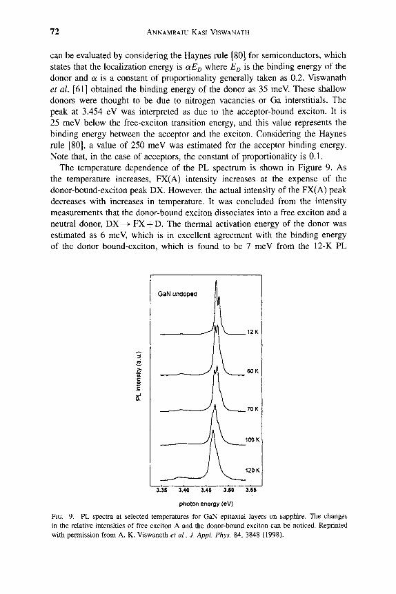
72 ANNAMRAJU KASI VISWANATH
can be evaluated by considering the Haynes rule [80] for semiconductors, which states that the localization energy is aEjy where E^^ is the binding energy of the donor and a is a constant of proportionality generally taken as 0.2. Viswanath et al. [61] obtained the binding energy of the donor as 35 meV. These shallow donors were thought to be due to nitrogen vacancies or Ga interstitials. The peak at 3.454 eV was interpreted as due to the acceptor-bound exciton. It is 25 meV below the free-exciton transition energy, and this value represents the binding energy between the acceptor and the exciton. Considering the Haynes rule [80], a value of 250 meV was estimated for the acceptor binding energy. Note that, in the case of acceptors, the constant of proportionality is 0.1.
The temperature dependence of the PL spectrum is shown in Figure 9. As the temperature increases, FX(A) intensity increases at the expense of the donor-bound-exciton peak DX. However, the actual intensity of the FX(A) peak decreases with increases in temperature. It was concluded from the intensity measurements that the donor-bound exciton dissociates into a free exciton and a neutral donor, DX ^- FX + D. The thermal activation energy of the donor was estimated as 6 meV, which is in excellent agreement with the binding energy of the donor bound-exciton, which is found to be 7 meV from the 12-K PL
3.35 3.40 3.45 3.50 3.55
photon energy (eV)
FIG. 9. PL spectra at selected temperatures for GaN epitaxial layers on sapphire. The changes in the relative intensities of free exciton A and the donor-bound exciton can be noticed. Reprinted with permission from A. K. Viswanath et al, J. Appl. Phys. 84, 3848 (1998).
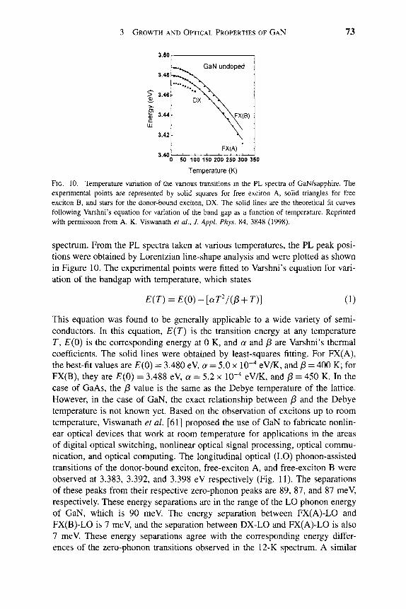
3 GROWTH AND OPTICAL PROPERTIES OF GAN 73
3.50
> 3.46 0)
, 3.44 h c LU
3.42
3.40
DX
-
GaN undoped
\ \ F X ( B )
FX(A) '
50 100 150 200 250 300 350
Temperature (K)
FIG. 10. Temperature variation of the various transitions in the PL spectra of GaN/sapphire. The experimental points are represented by solid squares for free exciton A, solid triangles for free exciton B, and stars for the donor-bound exciton, DX. The solid lines are the theoretical fit curves following Varshni's equation for variation of the band gap as a function of temperature. Reprinted with permission from A. K. Viswanath et al., J. Appl. Phys. 84, 3848 (1998).
spectrum. From the PL spectra taken at various temperatures, the PL peak posi-tions were obtained by Lorentzian Hne-shape analysis and were plotted as shown in Figure 10. The experimental points were fitted to Varshni's equation for vari-ation of the bandgap with temperature, which states
£(r) = £(0)-[arV(i3 + r)] (1)
This equation was found to be generally applicable to a wide variety of semi-conductors. In this equation, E{T) is the transition energy at any temperature r , £"(0) is the corresponding energy at 0 K, and a and j8 are Varshni's thermal coefficients. The solid lines were obtained by least-squares fitting. For FX(A), the best-fit values are £(0) = 3.480 eV, a = 5.0 x 10"^ eV/K, and /3 = 400 K; for FX(B), they are E{0) = 3.488 eV, a = 5.2 x 10"^ eV/K, and j3 = 450 K. In the case of GaAs, the j8 value is the same as the Debye temperature of the lattice. However, in the case of GaN, the exact relationship between j8 and the Debye temperature is not known yet. Based on the observation of excitons up to room temperature, Viswanath et al. [61] proposed the use of GaN to fabricate nonlin-ear optical devices that work at room temperature for applications in the areas of digital optical switching, nonlinear optical signal processing, optical commu-nication, and optical computing. The longitudinal optical (LO) phonon-assisted transitions of the donor-bound exciton, free-exciton A, and free-exciton B were observed at 3.383, 3.392, and 3.398 eV respectively (Fig. 11). The separations of these peaks from their respective zero-phonon peaks are 89, 87, and 87 meV, respectively. These energy separations are in the range of the LO phonon energy of GaN, which is 90 meV The energy separation between FX(A)-LO and FX(B)-LO is 7 meV, and the separation between DX-LO and FX(A)-LO is also 7 meV. These energy separations agree with the corresponding energy differ-ences of the zero-phonon transitions observed in the 12-K spectrum. A similar

74 ANNAMRAJU KASI VISWANATH
3 3^ ^ V) c
_ J Q .
GaN undoped |
12 K
DX-
1 FX(A) - LO /
[\ / / \ / /• \ F X ( B ) - L O /
J 1 1
3.35 3.40 3.45
photon energy (eV)
FIG. 11. Photoluminescence spectrum for GaN/sapphire at 12 K showing the phonon-assisted exciton transitions. The dotted lines show the fit to multiple peaks, assuring a Lorentzian line-shape function. Reprinted with permission from A. K. Viswanath et ai, J. Appl Phys. 84, 3848 (1998).
assignment was made by Dingle et al. [14], who observed a very weak dou-blet at 3.38 eV in their PL spectra at 1.6 K for GaN. They have assigned these transitions to phonon replicas of donor-bound and free excitons. The phonon replicas they observed were 90 and 88 meV below the corresponding zero-phonon lines. Phonon replicas due to longitudinal optical modes were observed by Kovalev et al. [32] in the free-exciton luminescence and photoluminescence excitation spectra of free excitons in GaN. Shan et al. [51] observed similar fea-tures in the photoluminescence excitation spectra of free and bound excitons in the photoluminescence excitation spectra of thin films of GaN. The observation of phonon replicas in excitonic transitions shows that phonon-assisted exciton formation is very efficient in GaN. In polar semiconductors there is a strong interaction between free excitons and LO phonons that is generally known as Frohlich polar intraband scattering [81]. This interaction is important in free-exciton recombination and kinetic energy relaxation within the exciton band. Similar phonon interactions were observed in other polar semiconductors like CdS [82-84], ZnSe [85], and CdSe [86].
The activation energy of the free exciton was estimated as 26 meV [61] from the PL intensities of the free exciton A as a function of l /T (Fig. 12). Monemar [15] reported a value of 28 meV for the exciton binding energy. Viswanath et al. [61] estimated the bandgaps of GaN as 3.505 and 3.437 eV at 12 K and room temperature, respectively. The band-structure calculation of Chen et al. [58], gave a room-temperature bandgap of 3.504 eV.
GaN epilayers as well as quantum well structures were also grown by molec-ular beam epitaxy [88-127]. Morkoc and co-workers [88, 89] reviewed the latest developments on this topic. In nitride growth, the main problem is to provide N species at sufficiently high rates. In gas-source MBE, gases instead of solid sources are used for group V elements. The options used for nitrogen include ammonia, electron cyclotron resonance (ECR), radiofrequency (rf), supersonic

3 GROWTH AND OPTICAL PROPERTIES OF GAN 75
1000
CO 1 0 0
GaN undoped Free exciton (A)
0.00 0.02 0.04 0.06 0.08 0.10
FIG. 12. PL intensities of the free-excition A transition (shown as stars) as a function of l/T. The activation energy of free exciton A is estimated as 26 meV from the slope of the straight line. Reprinted with permission from A. K. Viswanath et al., J. Appl. Phys. 84, 3848 (1998).
jet, and ion sources. In reactive molecular beam epitaxy (RMBE) ammonia is used, whereas in plasma molecular beam epitaxy (PMBE), plasma-activated nitrogen is used as the nitrogen source. Yoshida et al. [125] observed improve-ments in the electrical and luminescent properties in GaN epilayers grown by reactive molecular beam epitaxy by using an AlN-coated sapphire substrate, whereas Grandjean and Massies [128] utilized a GaN buffer layer. Botchkarev et al. [90] have grown GaN by electron cyclotron resonance-activated nitrogen under Ga- and N-rich conditions in a substrate temperature range of 650-850 °C. Strong band-edge photoluminescence was observed, with N-rich conditions that led to better mobilities and lower carrier concentrations. The optimum tem-perature for substrate was found to be 750 °C. Free-exciton transitions were observed by Jiang and co-workers [91, 93, 96] in a number of samples. Reynolds et al. [95] investigated emission and reflection spectra in the intrinsic region and the data were interpreted in terms of wurtzite crystal band structure. Three intrinsic exciton transitions were observed, one associated with each of the valence bands. Excited states of excitons associated with the top two valence bands were also observed. Reynolds et al. reported the exciton binding ener-gies, bandgap energies, and the exciton Bohr radii along with the dielectric constant and the spin-orbit and crystal-field parameters for GaN. Materials characteristics and growth kinetics of wurtzite GaN grown by reactive MBE were reported by Kim et al. [97]. All three intrinsic exciton transitions aris-ing from A, B, and C interband transitions were observed in reflectance mea-surements made by Liu et al. [98] on high-quality wurtzite GaN on sapphire. Petalas et al. [99] showed that the bandgap of hexagonal GaN is higher than that of the cubic polytype. The Burstein-Moss effect was observed in different GaN samples by Moustakas's group [100]. The effect of atomic hydrogen on the growth of GaN was studied by Yu et al. [102]. In phosphorous-mediated MBE, cubic GaN was achieved by Zhao et al. [103]. Photocurrent and photo-luminescence measurements were made by Komitzer et al. [106] on GaN epi-layers in which an AlN/GaN buffer layer was employed. Heinlein et al. [107]
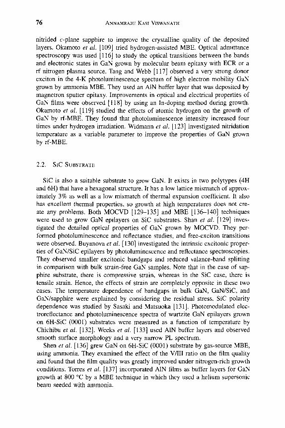
76 ANNAMRAJU KASI VISWANATH
nitrided c-plane sapphire to improve the crystalline quality of the deposited layers. Okamoto et aL [109] tried hydrogen-assisted MBE. Optical admittance spectroscopy was used [116] to study the optical transitions between the bands and electronic states in GaN grown by molecular beam epitaxy with ECR or a rf nitrogen plasma source. Tang and Webb [117] observed a very strong donor exciton in the 4-K photoluminescence spectum of high electron mobility GaN grown by ammonia MBE. They used an AIN buffer layer that was deposited by magnetron sputter epitaxy. Improvements in optical and electrical properties of GaN films were observed [118] by using an In-doping method during growth. Okamoto et al. [119] studied the effects of atomic hydrogen on the growth of GaN by rf-MBE. They found that photoluminescence intensity increased four times under hydrogen irradiation. Widmann et al. [123] investigated nitridation temperature as a variable parameter to improve the properties of GaN grown by rf-MBE.
2.2. SiC SUBSTRATE
SiC is also a suitable substrate to grow GaN. It exists in two polytypes (4H and 6H) that have a hexagonal structure. It has a low lattice mismatch of approx-imately 3% as well as a low mismatch of thermal expansion coefficient. It also has excellent thermal properties, so growth at high temperatures does not cre-ate any problems. Both MOCVD [129-135] and MBE [136-140] techniques were used to grow GaN epilayers on SiC substrates. Shan et al. [129] inves-tigated the detailed optical properties of GaN grown by MOCVD. They per-formed photoluminescence and reflectance studies, and free-exciton transitions were observed. Buyanova et al. [130] investigated the intrinsic excitonic proper-ties of GaN/SiC epilayers by photoluminescence and reflectance spectroscopies. They observed smaller excitonic bandgaps and reduced valance-band splitting in comparison with bulk strain-free GaN samples. Note that in the case of sap-phire substrate, there is compressive strain, whereas in the SiC case, there is tensile strain. Hence, the effects of strain are completely opposite in these two cases. The temperature dependence of bandgaps in bulk GaN, GaN/SiC, and GaN/sapphire were explained by considering the residual stress. SiC polarity dependence was studied by Sasaki and Matsuoka [131]. Photomodulated elec-troreflectance and photoluminescence spectra of wurtzite GaN epilayers grown on 6H-SiC (0001) substrates were measured as a function of temperature by Chichibu et al. [132]. Weeks et al. [133] used AIN buffer layers and observed smooth surface morphology and a very narrow PL spectrum.
Shen et al. [136] grew GaN on 6H-SiC (0001) substrate by gas-source MBE, using ammonia. They examined the effect of the V/III ratio on the film quality and found that the film quality was greatly improved under nitrogen-rich growth conditions. Torres et al. [137] incorporated AIN films as buffer layers for GaN growth at 800 °C by a MBE technique in which they used a helium supersonic beam seeded with ammonia.

3 GROWTH AND OPTICAL PROPERTIES OF GAN 77
2.3. ZNO SUBSTRATE
The lattice mismatch between GaN and ZnO is very small {s = 0.017) and there is a very good stacking order match. For this reason, stacking mismatch boundaries and inversion domain boundries do not occur if GaN is grown on ZnO. Morkoc's group initiated and developed this technique [141-144]. High-quality GaN epilayers have been grown on ZnO(OOOl) substrates by RMBE. It was shown by PL and reflectivity that the quality of samples is very high, which was attributed to matching of the stacking order. Sun et al. [145] have grown GaN on Sapphire using ZnO buffer layer. The ZnO buffer layer was grown by pulsed laser diposition technique. Surface morphology was improved by using the buffer layer of zinc oxide. PL results were also reported.
2.4. LiGa02 SUBSTRATE
The structure of LiGa02 (LGO) is similar to that of the wurtzite structure. Because Li and Ga atoms have different sizes, j8-LG0 is not a wurtzite crystal, but is orthorhombic. The atomic arrangement in the (001) face is hexagonal-like and, hence, growth of (001) GaN that matches the hexagonal symmetry in these two planes is possible. The lattice mismatch between GaN and LGO is only about 1-2%. Razeghi's group [146] grew GaN monocrystalline thin films on /3-LGO by the MOCVD technique and they examined the influence of growth temperature. Ishi et al. [147] used coaxial impact collision ion scattering spectroscopy to identify the surface atoms of a LiGa02 substrate for GaN thin film growth.
2.5. MgAl204 SUBSTRATE
MgAl204 has a spinel-type crystal structure {Fd3m). Mg and Al atoms occupy the tetrahedral and octahedral sites, and the oxygen atoms form a face-centered cubic sublattice. The lattice constant is 8.083 A and the lattice mis-match is 10% Kuramata et al. [148] grew GaN crystals by MOCVD on (111) and (100) MgAl204 substrates. In room-temperature PL, a band-edge emission at around 360 nm was dominant. They obtained a smooth cleaved (1100) facet of the GaN epilayer, which is normal to the surface, and was proposed for use as a cavity mirror in a laser diode. Khan's group [149, 150] used a GaN buffer layer in their MOCVD growth of GaN on (100) and (111) MgAl204 sub-strates. Nikishin et al. [151] grew high-quality wurtzite structure GaN layers on (111) MgAl204 by gas-source MBE. Hydrazine was used as the source of active nitrogen and excellent luminescent properties were observed.

78 ANNAMRAJU KASI VISWANATH
(0
[
^ * ^ ^
r ' vv* t Er\ r ^
h
^ Cubic /?-
"l 1 1 i 1 1 1 t 1 1 H 1 1 1
Eo+Ao
\ "XTX
i \ \
-GaN \
1 1 1 1 1 1 1 1 1 1 1 1 1 1 1
0 50 100 150 200 250 300
Temperature (K)
FIG. 13. Energies of the EQ (lower curve) and EQ + AQ (upper curve) transitions in zincblende struc-ture j8-GaN at temperatures between 10 and 300 K. Reprinted with permission from G. Ramirez-Flores et ai, Phys. Rev. B 50, 8433 (1994).
2.6. MgO SUBSTRATE
MgO has a face-centered cubic (fee) structure and offers the possibiUty of growing cubic GaN. The lattice mismatch between these two systems is 7.5%. An epitaxial metastable zincblende structure j8-GaN with a lattice constant of 0.4530 nm was grown pseudomorphically on cubic MgO (1 x 1) [152-154]. The temperature-dependent (10-300-K) optical bandgap EQ{T) was determined by modulated photoreflectance (Fig. 13). E^ in ^-GaN was found to vary from 3.302 eV at 10 K to 3.231 eV at 300 K. The spin-orbit splitting AQ in the valance band was determined to be 17 meV. The main transition in the photoreflectance was interpreted as due to radiative recombination from a shallow donor, at ^11 meV below the conduction-band edge and the valence band. The estimated refractive index was found to be smaller than the previously reported [155] value.
2.7. SI SUBSTRATE
Growth of GaN on Si substrate is a very important step in GaN technology, because it offers the possibility of integrated optoelectronics with Si technol-ogy, which is well established. Si substrates are cheap and very easily available. Both MOCVD and MBE techniques were tried to grow GaN on (100) and (111) Si substrates [156-169]. An important point to remember here is that the lattice mismatch between GaN and Si is quite large. To solve this problem, an interme-diate layer or series of layers is used; several semiconductor materials were tried for this purpose. Strittmatter [156] grew GaN on silicon (111) by low-pressure

3 GROWTH AND OPTICAL PROPERTIES OF GAN 79
MOCVD using Al as the nucleation layer, which is quite stable up to 1050 °C and, unlike GaN and AIN buffer layers, the formation of SiN^ on the Si surface is prevented. However, a thin GaN buffer layer was deposited at low temperature on the AlAs nucleation layer. Zhang et al. [157] grew GaN epilayers on silicon (001) substrate with specially designed composite intermediate layers consisting of an ultra thin amorphous silicon layer and a GaN/AlGaN multilayered buffer layer by MOCVD. They obtained good-quality epilayers. Ishikawa et al. [158] used a Si(ll l) substrate in their atmospheric pressure MOCVD method, and an intermediate layer consisting of AIN and AlGaN improved the optical quahty of GaN. Kobayashi et al. [159] showed in their MOCVD grown GaN epilayers that an aluminum oxide compound layer can be used as an intermediate layer. Steckl et al. [160] demonstrated that Si(l l l) semiconductor-on-insulator struc-tures were converted to SiC by carbonization of the thin (<100-nm) Si layer using rapid thermal chemical vapor deposition with mixtures of propane and H2 at atmospheric pressure. Cao et al. [161, 162] also used silicon-on-insulator substrates in their low-pressure MOCVD growth of GaN, and the quality of the epilayers was shown to be improved compared to Si substrate. The effect of Si doping on the structural quality of wurtzite GaN layers grown by MBE on AIN buffered Si(l l l) substrate was studied [163, 169]. Radiofrequency plasma-assisted MBE was employed to grow wurtzite GaN films on silicon nitride buffer layers formed on Si(l l l) substrate [164].
GaN thin films were grown by electron cyclotron resonance MBE on Si(l l l) wafers [165]. The mechanism for growth of single-crystal GaN on oxidized AlAs(AlO^) formed on a Si(l l l) substrate by MOCVD was examined by Kobayashi et al. [166]. Hiroyama et al. [167] investigated the effect of very thin SiC layer formation on Si(OOl) for cubic GaN growth by rf plasma-assisted MBE. Moustakas and co-workers [168] achieved both zincblende and wurtzite GaN films on (001) Si by electron cyclotron resonance mircrowave plasma-assisted MBE, using a two-step growth process. In all the preceding growth techniques, PL was utilized to check the quality of the samples.
2.8. GAAS SUBSTRATE
Though most of the work on GaN has been done on wurtzite structure, cubic form also is very useful for device applications. The crystal structure of GaN epilayers depends on the substrates and its symmetry. GaAs substrates can be used to grow cubic forms of GaN. Both MOCVD and MBE techniques have been employed to grow GaN epilayers on GaAs substrates [170-189]. Wurtzite as well as cubic forms of GaN were reported. Theoretical work predicted [190] that the cubic phase of GaN should possess much superior electronic proper-ties for device development. It is possible to integrate GaN devices on read-ily available, high-quality III-V semiconductor substrates that minimize lattice

80 ANNAMRAJU KASI VISWANATH
mismatch with the nitride structure. c-GaN is expected to have a higher mobil-ity due to lower phonon scattering in the higher crystallographic symmetry. The c-GaN epilayers can be easily cleaved along a substrate facet, and it can be used as a cavity mirror for semiconductor lasers. It was also shown theo-retically that C-GaN quantum wells may have higher optical gain [191]. Hong et al. [170] found that the photolumincescence characteristics remained invari-ant with the material phase. A free-exciton energy of 3.375 eV was deduced at 6.5 K. The thermal stability of c-GaN was investigated by PL studies [172]. The influence of the As autodoping effect from GaAs substrates on c-GaN grown by halide vapour phase epitaxy and metal organic molecular beam epitaxy was investigated by Tsuchiya et al. [175] by PL techniques. By plasma-assisted low-pressure MOCVD, cubic and hexagonal GaN films were grown on (001) GaAs substrates. Cubic GaN was grown under Ga-rich conditions and c-axis-oriented hexagonal GaN was obtained under N-rich conditions. A very comprehensive investigation of the optical properties of plasma-assisted MBE grown c-GaN on vicinal (100) GaAs substrates was reported by Morkoc and co-workers [177]. In cathodoluminescence, mid-gap states and band-edge transitions were recorded. The room-temperature bandgap of c-GaN was given as 3.45 eV. Synthesis of GaN by N ion implantation in GaAs (001) was achieved by Lin et al. [178]. A phase transition from cubic to hexagonal phase was also observed when the sam-ples were subjected to extended thermal annealing. Bandgaps of both cubic and hexagonal films obtained by modified MBE techniques were reported by Lack-lison et al. [179]. They also noted that errors made in the literature in reporting the bandgaps of GaN were due to the existence of the mixed phase in the sam-ples. Ploog and co-workers [180] characterized hexagonal and cubic phases of GaN by spatially resolved cathodoluminescence spectra from micrometer-size single crystals grown by plasma-assisted MBE. The near-band-edge PL of cubic GaN grown by rf plasma-assisted MBE was measured by As et al. [184]. They observed excitonic and donor-acceptor pair transitions. Optical second harmonic spectroscopy [185] was used to probe the interface electronic structure of highly mismatched j8-GaN/GaAs(001) heterostructures in the vicinity of the interband critical point of j8-GaN. Detailed reflectivity studies of hexagonal GaN films grown by MBE on GaAs substrates were reported by Shokhovets et al. [187]. Optical constants of cubic GaN were determined by Kohler et al. [188] by com-bined reflectivity and spectroscopic ellipsometry studies.
2.9. GAN SUBSTRATE
To optimize LEDs and semiconductor lasers, it is necessary to reduce the concentration of defects in the epilayers. The best way to accomplish this is by homoepitaxy in which GaN epitaxial layers are grown on GaN substrates. Porowski's group [192-194] was very successful with this approach and they have grown good quality GaN epilayers on GaN substrates. They have also

3 GROWTH AND OPTICAL PROPERTIES OF GAN 81
3
JO a
^ (0
o =
: ^ / 1
- " ^ A
jf Jr
T = 42K
B 1 ^
1 1 1
C
345 346 347 348 349 350
Energy [eV|
351 3 52
FIG. 14. The experimental reflectance spectrum of the GaN layer at T = 4.2 K with fitted theoret-ical curve. Three exciton lines originate from the crystal field and spin-orbit splitting of the valence band. Reprinted with permission from K. P. Korona et al., Appl. Phys. Lett. 69, 788 (1996).
developed large area GaN substrates. Very narrow lines were observed in PL and very weak yellow luminescence due to defects was noticed. In the photore-flection experiments (Fig. 14), three-free exciton lines were observed. The spin-orbit parameter A ^ = 19.7 meV and crystal-field parameter A r = 9.3 meV were reported. Thick GaN (10-30 /xm) was grown for the first time on sapphire sub-strates using a sublimation method by Kurai et al. [195]. Naniwae et al. [196] have grew single crystal GaN substrates by hydride vapor phase epitaxy.
2.10. LATERAL EPITAXIAL OVERGROW^TH
Selective area epitaxy of semiconductors in which Si02 masks are used in the MOCVD technique to grow high-quality materials is very well known in the lit-erature [197]. Several groups have reported [198-219] the use of selective area epitaxial overgrowth to grow high-quality GaN. In this technique, the idea is to reduce the density of defects. Growth rate anisotropics that occur during GaN selective epitaxy cause pyramid structures to result from growth in small two-dimensional mask features [199]. Figure 15 shows the schematic for the lateral epitaxial overgrowth of a GaN layer on Si02 mask. Nam et al. [202] achieved lateral overgrowth of GaN stripes patterned in a Si02 mask deposited on GaN film/AlN buffer layer/6H-SiC(0001) substrate. Lateral overgrowth was accom-plished by depositing GaN on the underlying GaN layer through windows in the Si02 mask. Kawaguchi et al. [205] studied the selective area growth of GaN on (111) Si substrate using AlGaN as an intermediate layer. In the cathodolu-minescence of the submicrometer dots of GaN, strong near-band-edge emission was observed. Freitas et al. [206] reported high resolution optical properties of homoepitaxial GaN layers deposited by organometallic vapor phase epitaxy

82 ANNAMRAJU KASI VISWANATH
Overgrown GaN Layer
SiOiMask (O.lfim)
6H-SiC(000I)
FIG. 15. Schematic that shows the lateral epitaxial overgrowth of a GaN layer on an Si02 mask from GaN deposited within striped window openings on GaN/AlN/6H-SiC substrates. Reprinted with permission from O. H. Nam et ai, AppL Phys. Lett. 71, 2638 (1997).
on stripe-patterned GaN films on 6H-SiC substrates. Figure 16 shows the low-temperature PL spectra excited with a 60-)Ltm-diameter laser beam incident on a region of the sample where Lateral epitaxial overgrowth (LEO) had devel-oped from 3-mm-wide stripes. A very weak yellow band (2.25 eV), the edge emission band (3.467 eV), and an intense donor-aceptor pair (DAP) band with zero-phonon line (ZPL) at 3.263 eV and with phonon replicas at 3.173, 3.083, and 2.292 eV were observed. The PL spectrum of the GaN/AlN/SiC substrate (Fig. 16b) does not shown the DAP band.
3
c B c Q.
-1 1 r——1—
6K
325 nm
a)
1 1 1 1
— 1 r r T • • • • T —
substrate layer
10 j
homoepitaxial layer
DAP (ZPL)
1 ILO 1
2Lol n
^^°\ A \ ^ J ^ V J
i 1 1 .... 1 .. 1
L
1.8 2.0 2.2 2.4 2.6 2.8 3.0 Energy (eV)
3.2 3.4
FIG. 16. Low resolution PL spectrum of (a) the 3-/Am uncoalesced strips and (b) the GaN/6H-SiC substrate. Reprinted with permission from J. A. Freitas, Jr. et ai, Appl. Phys. Lett. 72, 2990 (1998).

3 GROWTH AND OPTICAL PROPERTIES OF GAN 83
— X 0* 325 nm
3.42 3.44 3.46 Energy (eV)
3.48 3.50
FIG. 17. Near-band-edge PL spectra of 3-/Ltm uncoalesced strips at different temperatures. Note the absence of a line at 3.4643 eV (Dj) in curve (g), the 50-K spectrum of the GaN substrate. Reprinted with permission from J. A. Freitas, Jr. et ai, Appl. Phys. Lett. 72, 2990 (1998).
To identify the impurities associated with the PL signal, high resolution experiments were done. The temperature dependence of PL is shown in Figure 17. The PL spectrum of the underlying GaN film shows two peaks that were attributed to free exciton A (3.4725 eV) and to a donor-bound exciton (3.4667 eV). The PL spectra of all uncoalesced stripes show an additional band at 3.4643 eV that was attributed to a deeper second donor based on tempera-ture dependence studies. Figure 18 shows the low-temperature higher spectral resolution PL spectra from 3-/xm uncoalesced stripes and the GaN substrate region. The smaller feature at 3.4505 eV is assigned to an oxygen-related defect. Wang et al. [208] tried lateral overgrowth by the sublimation technique. Spa-tially resolved cathodoluminescence was used at each stage of the growth along with wavelength imaging, and an improvement in the optical quality was shown [210]. A similar technique was adopted by Bertram et al.[2\\\ Zeng et al. [213] studied the optical properties of GaN pyramids fabricated by the selective epi-taxial overgrowth (SEO) method. A schematic of the pyramids is shown in Figure 19.
Comparison of various properties of undoped GaN that are obtained from the PL spectra and other optical techniques are given in Tables II-VL These proper-ties include free-exciton transition energies, PL peak positions and localization

84 ANNAMRAJU KASI VISWANATH
I
S 2
6K 325 nm (20nm spot)
- i 1 1 1 v
homocpilaxial (layer)
/
3.40 3.42 3.50
FIG. 18. Low-temperature higher spectral resolution PL spectra from 3-/im uncoalesced strips and GaN substrate regions. The laser spot was ~20 jim. Note the new features at ~3.4506 and 3.4642 eV, and the relative blue shift (—1.5 meV) of Dp FX^, and FXB in the overgrown GaN spectrum. Reprinted with permission from J. A. Freitas, Jr. et ai, Appl Phys. Lett. 72, 2990 (1998).
energies of donor- and acceptor-bound excitons, Varshni's coefficients, and bind-ing energies of the free exciton (A).
3. Line Width and Quantum Beats in GaN
When semiconductors are optically excited, several interactions take place among excitons, free carriers, lattice phonons, impurities, and defects. Such interactions have been studied in bulk and quantum-confined semiconduc-tors by absorption, luminescence, coherent spectroscopies in time, and fre-quency domain. In particular, the coupling between excitons and phonons is an important parameter in determining the electronic and optical properties of semi-conductors. The applicability of GaN and related materials from the point of view of exciton devices depends on the strength of the room-temperature exciton
GaN pyramids
0.2 |xm SiOj " t-
AIN Buffer - 4
sapphire or silicon
FIG. 19. Schematic showing GaN pyramids fabricated by selective epitaxial overgrowth on the GaN/AlN/Si or GaN/AlN/sapphire substrates. Reprinted with permission from K. C. Zeng et al., Appl Phys. Lett. 74, 1227 (1999).
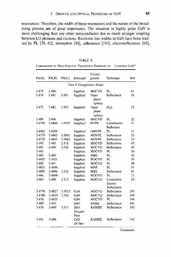
3 GROWTH AND OPTICAL PROPERTIES OF GAN 85
resonances. Therefore, the width of these resonances and the nature of the broad-ening process are of great importance. The situation in highly polar GaN is more challenging than any other semiconductor due to much stronger coupling between LO phonons and excitons. Excitonic line widths in GaN have been stud-ied by PL [29, 62], absorption [50], reflectance [193], electroreflectance [65],
TABLE II
COMPARISON OF FREE-EXCITON TRANSITION ENERGIES IN UNDOPED GAN''
FX(A)
3.479 3.474
3.475
3.488 3.4799
3.4962 3.4770 3.4775 3.485 3.491 3.483 3.483 3.4857 3.485 3.4831 3.4903 3.484 3.484
3.4776 3.4780 3.478 3.480 3.476
3.481
FX(B)
3.486 3.481
3.481
3.496 3.4860
3.5050 3.4865 3.4845 3.493 3.499
3.489 3.4921 3.491 3.4896 3.4996 3.4899 3.490
3.4827 3.4835 3.4835 3.493 3.489
3.496
FX(C) Substrate^ Crystal growth
Case I. Compressive Strain
3.501
3.493
3.5025
3.5062 3.5062 3.518 3.528
3.525
3.512
3.5015 3.502
3.511
Sapphire Sapphire^
Sapphire'
Sapphire Sapphire'
Sapphire^ Sapphire Sapphire Sapphire Sapphire Sapphire Sapphire Sapphire Sapphire Sapphire Sapphire Sapphire Sapphire
GaN GaN GaN ZnO ZnO Oxygen Face ZnO Zn face
MOCVD Vapor
phase epitaxy
Vapor phase epitaxy
MOCVD HVPE
OMVPE MOVPE MOVPE MOCVD MOCVD MOCVD MBE MOCVD MOCVD MBE MBE MOCVD MOCVD
MOCVD MOCVD MOCVD RMBE RAMBE
RAMBE
Technique
PL Reflectance
PLE
PL Calorimetric Reflection PL Reflectance Reflectance Reflectance Reflectance PL PL PL PL PL Reflectance PL Contactless Electro Reflectance Reflectance Reflectance PL Reflectance Reflectance
Reflectance
Ref.
61 14
15
22 31
31 52 53 45 49 56 93 59 58 91 91 71 65
193 194 194 141 142
142
Continued..

86 ANNAMRAJU KASI VISWANATH
TABLE II CONTINUED
FX(A)
3.4703 3.4795 3.470 3.472 3.470 3.454 3.47-
3.49 3.372 3.274
FX(B)
3.474
FX(C)
3.491
3.486 3.475
Substrate'' Crystal growth
Case II. Tensile Strain
6H-SiC^ 6H-SiC^ 6H-SiC 6H-SiC 6H-SiC Si(l l l) Si(l l l)
GaAs (100) GaAs (100)
OMVPE OMVPE MOCVD HVPE MOVPE MOVPE GSMBE
MOCVD MOVPE
Technique
PL PL Reflectance PL PL PL PL
PL PL
Ref.
31 31
48,129 130 132 132 257
170 173
''Abbreviations: MOCVD, metal-organic chemical vapor deposition; HVPE, hydride vapor phase epitaxy; OMVPE, MOVPE, organometallic and metallic vapor phase epitaxy; MBE, molecular beam epitaxy; PIMBE, plasma-induced molecular beam epitaxy; GSMBE, gas source molecular beam epitaxy; RMBE, reactive molecular beam epitaxy; RAMBE, reactive ammonia molecu-lar beam epitaxy; PL, photoluminescence; PLE, photoluminescence excitation. ''Unless otherwise noted, all samples have thicknesses in the range of 3 /Am. ^ These values are for strain-free thick samples of bulk GaN. "^Sample thickness 400 /xm. ^Sample thickness 3 /im. ^Sample thickness 80 ijum. Source: A.K. Viswanath et ai, J. Appl. Phys. 84, 3848 (1998).
spectroscopic ellipsometry [99], thermomodulation [66], and time-integrated (TI) and spectrally resolved (SR) degenerate four-wave mixing (DFWM) [220]. Several groups have performed nonlinear spectroscopic experiments such as degenerate and nondegenerate four-wave mixing, pump-probe spectroscopy of GaN to understand very interesting phenomena like exciton-phonon interac-tions, the lifetime of excitons, quantum beats, self-induced transparency, exciton dephasing, exciton-exciton interaction, hot electron relaxation, and second har-monic generation [220-229].
Different authors have considered different origins for the line width, and the broadening parameters also scan a wide range. It is important to understand the exciton line widths in photoluminescence, because the photonic devices are based on emission phenomena. In fact, the lasing mechanism in GaN-based devices—excitonic versus band-to-band recombination—has not been explicated so far, and this topic is currently under intense debate [230]. Therefore, the properties of excitons in these systems, particularly those that depend on tem-perature, are very important, because they can shed some light on some of the critical issues.

3 GROWTH AND OPTICAL PROPERTIES OF GAN 87
TABLE III
COMPARISON OF PL PEAK POSITIONS AND LOCALIZATION ENERGIES OF
DONOR-BOUND EXCITONS IN GAN
Crystal growth
MOCVD MOCVD Vapor phase
epitaxy Vapor phase
epitaxy OMVPE OMVPE HVPE HVPE MOCVD MOCVD MOCVD MBE MOCVD MBE MOCVD PAMBE MOCVD RMBE
OMVPE OMVPE OMVPE GSMBE
Substrate
Case L
Sapphire Sapphire Sapphire''
Sapphire''
Sapphire Sapphire Sapphire Sapphire Sapphire Sapphire Sapphire Sapphire Sapphire Sapphire Sapphire Sapphire GaN ZnO
Peak position (eV)
Compressive Strain
3.472 3.481 3.466-3.468
3.469
3.4935 3.4900 3.4727 3.4762 3.477 3.479 3.476 3.475 3.476 3.474 3.484 3.474 3.4719 3.364
Case IL Tensile Strain 6H-SiC 6H-SiC 6H-SiC Si(ll l)
3.4639 3.4723 3.466 3.456
Localization energy (meV)
7 7 6-8
6.4
2.7 6.2 7.7 3.7 6 6 7 7.5 8-9
— 5.9
— 6.1
11
6.4 7.2 6.0 7-9
Ref.
61 22 14
15
31 31 31 31 28 45 56 93 58 91 71 96
194 141
31 31
130 257
''Values are for strain-free thick samples of bulk GaN. Source: A.K. Viswanath et al, J. Appl. Phys. 84, 3848 (1998).
Viswanath et al. [62] performed a detailed analysis of exciton line widths in the PL of GaN. Figure 20a and b shows the temperature dependence of the line widths of the free excitons A and B, respectively. Solid circles denote experimental line widths. The observed line widths were fitted to a theoretical model.
Line broadening in semiconductors has been considered theoretically by var-ious workers. The basic formalism for phonon-assisted optical absorption and exciton lifetimes was developed by Toyozawa [231] and Segall and Mahan [232]. Segall [233] applied it to described absorption and emission in a number of materials. In this formalism, light absorption by an exciton was discussed in the context of linear-response theory. The absorption is given by an imaginary

88 ANNAMRAJU KASI VISWANATH
TABLE IV
COMPARISON OF PL PEAK POSITIONS AND LOCALIZATION ENERGIES OF
ACCEPTOR-BOUND EXCITONS IN GAN
Crystal growth
MOCVD MOCVD
Vapor phase epitaxy
MOCVD MOCVD MOCVD MOCVD
GSMBE
Substrate
Case L Sapphire Sapphire
Sapphire
Sapphire Sapphire Sapphire GaN
Peak position (eV)
Compressive Strain 3.454 3.4805 3.4633 3.455
3.459 3.459 3.455 3.4666
Case n. Tensile Strain Si(ll l) 3.446
3.436
Localization energy (meV)
25 11.6 28.8 19
— 25 22.2 11.4
24-44 34-54
Ref.
61 23
14
57 58 71
194
257
Source: A.K. Viswanath et al, J. Appl Phys. 84, 3848 (1998).
TABLE V
VARSHNI'S COEFFICIENTS FOR GAN AND COMPARISON WITH REPORTED
VALUES OBTAINED FROM DIFFERENT EXPERIMENTAL TECHNIQUES
Experimental technique
Photoluminescence of FX(A) FX(B)
Photoluminescence excitation Photoluminescence of donor Bound exciton Absorption of epilayer Absorption of bulk sample Photoreflection of FX(A)
FX(B) FX(C)
Absorption of FX(A) Reflectance of FX(A)
FX(B) FX(C)
Absorption of MOCVD sample Absorption of MBE sample Spectroscopic ellipsometry
Reflectance of zincblende GaN Thermomodulation
a/10-^ eV/K
5.0 5.2
-5.08 7.2
9.39 10.8 8.32
10.9 2.92
11.8 12.8 12.9 6.6 5.66
11.56 8.58 6.06 6.697 5.9
i8(K)
400 450
-996 600
772 745 835.6
1194 3698.9 1414 1190 1280 840 737.9
1187.4 700 (fixed) 800 (fixed) 600 600
Ref.
61 61 15 14
100 100 47
50 65
67 67 99
152 66
Source: A.K. Viswanath et al, J. Appl Phys. 84, 3848 (1998).

3 GROWTH AND OPTICAL PROPERTIES OF GAN 89
TABLE VI
BINDING ENERGIES OF FREE EXCITON A IN GAN
Estimation method Binding energy
(meV) Ref.
Temperature dependence of FX(A) transition in PL
Calculated using the values of electron and hole effective masses
Peak separation between FX(A) and E^ obtained from the PLE spectra
From the excited state PL of FX(A) Temperature dependence of FX(A)
transition in PL From the excited state photoreflectance
of FX(A) From the excited state PL of FX(A) Band structure calculation using local
density approximation From the excited state PL of FX(A)
26
27
28
26.1 26.7
21
18.3 20
61
22
15
31 32
49
59 58
20 95
Source: A.K. Viswanath et al, J. Appl Phys. 84, 3848 (1998).
part of the exciton Green's function and has a Lorentzian shape. The tempera-ture dependence of the width of the lowest IS exciton in semiconductors was initially reported by Segall [234], and the most comprehensive treatment was later given by Rudin, Reinecke, and Segall [235]. According to them, the exci-ton line width T{T) at any temperature T can be written as
nT) = T, + y^J + T^oN^oiJ) (2)
In high-purity crystals, the line width orignates from interactions with ther-mal phonons. In polar semiconductors, it is dominated by LO-phonon broad-ening. Actually, in any semiconductor grown by any method there are some background impurities and crystal imperfections, and they contribute to inhomogeneous broadening. This is represented as FQ in Eq. (2). At very low temperatures, phonons are not active and the contribution to the line width is mainly from inhomogeneous broadening. FQ is obtained by extrapolation of the Hne width to 0 K. The second and third terms on the right-hand side of Eq. (2) are the homogeneous line widths that are due to acoustic-phonon and LO-phonon scattering, respectively. The processes that involve acoustic phonons are only intraband scattering of excitons. The contribution due to acoustic phonons increases linearly with temperature T and is represented as y^^J, where y^^ is the exciton-acoustic-phonon coupling strength. The last term in Eq. (2) arises from interactions with LO phonons and is proportional to the Bose function A^Lo( ) fo^ LO-phonon occupation, which is equal to \/[tx^{hv^Q/kT — 1)], where hv^^Q is the LO-phonon energy in GaN and F^o represents the strength

90 ANNAMRAJU KASI VISWANATH
25
20
> 15 <D
Z! 10
5
0
undoped GaN _FX(A)
1
T ^ ^ ^ »
r,oA«xp(h.
. . .X, ._j
(a)
• / . r,*r,o/lexp(hv,o/kT)-i]
1 . 1 . 1 . _ . . 1
0 50 100 150 200 250 300 350 400
Temperature (K)
undoped GaN FX(B)
ro*Tp,T + r,o/Iexp(hv^o/kT)-11
(b)
r„+r,o^exp(hv^ /kT)-i]
Temperature (K)
FIG. 20. Temperature dependence of the linewidths of (a) free exciton A and (b) free exciton B in GaN. Solid circles are the experimental points. The solid curve is the fitting of the experimental line widths considering acoustic-phonon scattering and LO-phonon scattering. Dashed lines show the contribution from the acoustic-phonon scattering alone and dotted lines show the contributions from the LO phonons only. In both cases, inhomogeneous broadening was added. Reprinted with permission from A. K. Viswanath et ai, Phys. Rev. B 58, 16, 333 (1998).
of excition-LO-phonon coupling. The Frohlich interaction describes the inter-actions of excitions with LO phonons. Phonons can scatter the excitons to the same bound state or to higher-lying bound states.
The solid lines in Figure 20 represent the least-squares fitting considering acoustic-phonon scattering and LO-phonon scattering in addition to inhomo-geneous broadening. The LO-phonon energy was taken as 91.5 meV [236, 237]. The hexagonal GaN crystallizes in the wurtzite structure belonging to the Qy(P63 mc) space group. There are two formula units per primitive cell and all the atoms occupy the sites of symmetry C-^^. In Raman spectroscopy, six optical modes, A (TO), A (LO), E (TO), ^Ej (LO), and ^E^ at

3 GROWTH AND OPTICAL PROPERTIES OF GAN 91
533, 735, 561,743, 144, and 569 cm-1 were observed. Here LO is longitudi-nal optical mode and TO stands for transverse optic mode. The fitting param-eters are TQ = 2.8 meV, y^^, = 21 ^eV/K, and FLO = 525 meV for FX(A) and To = 1.4 meV, y^^, = 22 ^teV/K, and T^Q = 495 meV for FX(B).
In Figure 20, the dashed lines represent the contribution from acoustic-phonon scattering and the dotted lines denote the contribution from LO phonons to the line width. In all cases, the inhomogeneous broadening is also added. The acous-tic phonons contribute up to 120 K, which is very significant, but the contribu-tion from LO phonons is negligible up to this temperature. Above 120 K, the LO-phonon contribution is very significant and the line width increases sharply, because of the exponential factor. At 200 K there is a crossover and LO phonons dominate over the acoustic phonons.
Line-width broadening parameters for free-exciton transitions in GaN are given in Table VII. The value of exciton-LO-phonon coupling parameter, FLQ, reported by Viswanath et al. [62] is very high, which indicates a very strong interaction between excitons and LO phonons. GaN is a polar material and has a very high Frohlich constant [238], which is responsible for the large FLQ value. Exciton-phonon interactions can be seen in the optical spectra in two ways: (1) the fine broadening of absorption or emission spectra and (2) the occurrence of phonon-assisted transitions in the absorption and emission spectra [14, 32, 51, 61] as discussed in the previous sections. The broadening parame-ters reported by Viswanath et al. [62] compare well with the four-wave mixing results of Fischer et al. [220]. The exact determination of the exciton-phonon coupling parameter is from spectrally resolved degenerate four-wave mixing. In
TABLE VII
LINE-WIDTH BROADENING PARAMETERS FOR FREE-EXCITON TRANSITIONS IN
GAN
^ LO Tph
Technique (meV) (^eV/K) Ref.
Photoluminescence of free exciton A free exciton B
Spectrally resolved degenerate four-wave mixing
Time-integrated degenerate four-wave mixing
Absorption of free exciton A Photoluminescence of free exciton A Reflectance of free exciton A Electroreflectance of free exciton A
free exciton B Spectroscopic ellipsometry Thermomodulation spectroscopy
Source: A.K. Viswanath et al, Phys. Rev. B 58, 16,333 (1998).
525 495 470
390
375 165 208 60 74 104 179
21 22 13
16
15 — 15.3
— — — —
62 62 220
220
50 29 193 65 65 99 66

92 ANNAMRAJU KASI VISWANATH
these measurements, the excitonic contribution is several orders of magnitude larger than the free-carrier contribution. The results obtained from other exper-iments such as absorption contain errors due to free-carrier contributions.
We compared the broadening parameters in GaN with those for other wide-bandgap II-VI [239-244] and III-V [245-247] semiconductors. Fischer et al. [239] performed degenerate four-wave mixing experiments and reported a value of FLO as 81 meV. Li et al. [241] gave a value of 400 meV for FLO based on their PL experiments. However, the values reported by other researchers based on absorption and luminescence were very low in the range of 16-25 meV for CdZnTe-type single and multiple quantum wells [242-244]. The deduced val-ues of FLO for GaAs and InGaAs bulk and quantum wells from the absorption and reflection experiments were small in the approximate range of 5-10 meV [245-247]. To understand this trend in FLO, the polarity of the material, which increases in the order GaAs, ZnTe, ZnSe, and GaN, has to be considered. The FLO value is also very much influenced by the energy of LO phonons. In GaN, the hv^Q value is very high (91.5 meV). For other semiconductors, the corre-sponding values are small: GaAs, 36.8 meV; ZnTe, 25.5 meV; ZnSe, 30.5 meV; CdTe, 21.2 meV; CdSe, 26.1 meV [235].
The 7ph represents the acoustic-phonon and exciton interaction. In the line-width analysis of GaN, most works [29, 65, 66, 99] did not consider the contributions of acoustic phonons. Lee, Koteles, and Vassell [248] gave the theoretical treatment of exciton-acoustic-phonon interactions. The y^^i value of Viswanath et al. [62] agrees with other reported values [50, 193, 220]. Lee et al. [248] predicted that acoustic phonons contribute up to 120 K to broadening of the line width. The origin of exciton-acoustic-phonon interactions is due to deformation potential and piezoelectric interaction. The differences in y^^ value can be thought of as due to differences in the deformation potentials in different samples. It is interesting to compare the y^^ value in GaN with other III-V and II-VI semiconductors. The y^^ values were reported as 4.6 /xeV/K for GaAs quantum wells, 11.0 JJLCV/K for ZnSe bulk as well as multiple quantum wells (MQW) of ZnCdSe/ZnSe [9] and 13.6 /JLCV/K for MQW of CdTe/CdMnTe [10]. This shows that the ^p^ value is in the same range for all the semiconductors. This is because yp depends on deformation potentials only and the Frohlich constant has no effect on it.
These exciton-acoustic-phonon interactions also explain the fast energy relax-ation of free excitons to the bottom of the exciton band, which leads to gen-erally observed short free-exciton lifetimes in GaN. This approach was also used recently to explain the quantum confinement effects on the magnitude of acoustic- and optical-phonon scattering in ZnCdSe/ZnSe MQW [249] and InGaAs/GaAs single quantum wells [250] by time-integrated degenerate four-wave mixing.
It is necessary to have excitons that can exist up to room temperature to realize room-temperature photonic devices. The existence of room-temperature excitons depends on the delicate balance between two competing factors. The first is the

3 GROWTH AND OPTICAL PROPERTIES OF GAN 93
exciton-LO-phonon interaction parameter and the second is the exciton binding energy. A very large value of r^o broadenes the exciton line so much so that, at high temperatures, the line vanishes completely. However, the larger binding energy of the exciton can resist the phonon interaction and it is possible to observe room-temperature excitons. This is what actually happens in the case of GaN, which has a larger binding energy of 26 meV. Viswanath et al. [62] suggested that to realize stable room-temperature devices, it is better to work with quantum-confined systems of GaN, which have higher binding energy and lower LO-phonon coupling as a direct consequence of quantum phenomena. Added to this, quantum wells have much narrower emission due to smaller inhomogeneous broadening.
Fischer et al. [220] were first to perform spectrally resolved and time-integrated degenerate four-wave mixing of GaN. They showed that excitonic resonances are nearly homogeneously broadened even at low temperatures. The temperature-dependent dephasing rate is used to deduce exciton-phonon inter-action rates. TI-DFWM shows strong beating between A and B excitons, and the beats were shown to be true quantum beats. Pau et al. [221] investigated the density and temperature dependence of the exciton dephasing time of two hexag-onal GaN films on sapphire by DFWM. The residual 4-ps dephasing time at low temperature and density was thought to be due to exciton-impurity scatter-ing. Pau et al. [222] also performed the experiments for different laser energies and intensities. They observed neither polariton effects nor exciton-free-carrier scattering. Exciton-exciton scattering was found to be the dominant dephasing mechanism at higher excitation densities. Zimmermann et al. [223] observed quantum beats between A and B excitons with a beat period of 0.520 ps, corre-sponding to an A-B splitting of 7.98 meV in the DFWM experiments (Fig. 21). Nondegenerate nanosecond optical pump-probe experiments were conducted by Schmidt et al. [IIA]. At higher excitation intensities, the A and B exciton reso-nances were broadened and decreased in intensity due to the presence of high-density photoexcited free carriers, and were completely absent in the absorption and reflection spectra as the excitation density approaches 3 MW/cm^, resulting in induced transparency in transmission experiments. Induced absorption was also observed below the bandgap at 10 K.
Haag et al. [225] determined the third order nonlinear susceptibility x^^"^ of GaN in degenerate four-wave mixing experiments in a two beam configuration at low temperatures. Haag et al. [226] investigated in great detail the nonlinear optical probes in GaN by doing many elegant experiments such as pump-probe, degenerate four-wave mixing with nanosecond and picosecond excitation under variable experimental conditions like excitation intensity and wavelength of the laser, temperature of measurement, and different delays for detection. They stud-ied both absorption and reflection. Figure 22a shows the linear reflection and absorption spectra and Figure 22b shows the emission spectrum in which reaso-nances due to both A and B were observed. The absorption spectra for different

94 ANNAMRAJU KASI VISWANATH
-0.5 0.0 0.5 1.0
Time Delay (ps)
3.480 3.485 3.490 3.495 3.500 3.505
Photon Energy (eV)
3.510 3.515
FIG. 21. (a) Time-integrated FWM for an excitation energy of 3.498 eV, that is, between the A and B excitons at low temperature (10 K) and low exciton density (< 5 x 10'^ cm~^). (b) Spectrum of the FWM signal at r = 0.38 ps. Reprinted with permission from R. Zimmermann et al, Phys. Rev. B 56, R12, 722 (1997).
delays t between test and pump pulses are shown in Figure 23, keeping the exci-tation intensity constant. At temporal coincidence, band filling effects are first observed, leading to quenching of the excitonic resonances. After excitation, a rapid decay is observed, which is characteristic of the time restitution of the excitonic resonances. Then, following a delay of about 40 ps after excitation, the excitonic resonances were observed again with a red shift of 8 meV that was attributed to heating of the sample induced by the laser pulses. Figure 24 shows the absorption spectra for different intensities of pump pulses, keeping the photon energy constant. It can be seen that with increase in the excita-tion intensity, there is a decrease in the absorption, along with a red shift for both A and B excitons. This again was thought to be due to sample heating.

3 GROWTH AND OPTICAL PROPERTIES OF GAN 95
3.48 3.50 352 3.54 Energy (eV)
FIG. 22. (a) Measured linear reflection (dotted line) and absorption (open circles) spectra of a 0.35-)Ltm-thick GaN film at 2 K and normal incidence. The fit of the absorption spectra is shown by the full line, (b) Emission spectrum of the sample excited at 4.024 eV at low intensities (thin line). The luminescence is corrected for reabsorption (open circles) and deconvoluted (full line) into three Gaussian lines (dashed-dotted lines). Reprinted with permission from H. Haag et al., Phys. Rev. B 59, 2254 (1999).
Figure 25 shows the absorption spectra for different photon energies of excita-tion, keeping the excitation intensity constant. The excitonic resonances A and B are smeared out and the absorption decreases when the photon energy of the pump beam is tuned into exciton resonance. Contrary to the band-to-band exci-tation as a function of intensity, thermal effects are only slightly observed here.
n (5
o
<
3.45 3.50 3.55
Energy (eV)
FIG. 23. Absorption spectra for different delays t between test and pump pulses of 4^ = 87 kW/cm^ (squares, r = 0 ps; circles, t — 25 ps; dots, t = 40 ps; line, r = 1.5 ns; bold line, linear absorption). Reprinted with permission from H. Haag et al., Phys. Rev. B 59, 2254 (1999).

96 ANNAMRAJU KASI VISWANATH
3
n <
3.45 3.50
Energy (eV)
3.55
FIG. 24. Absorption spectra at 2 K when the sample is excited at 4.024 eV with nanosecond pulses of different intensities: (a) 0 kW/cm^; (b) 8 kW/cm^ (c) 14 kW/cm^ (d) 24 kW/cm"^ (e) 38 kW/cm~'; (f) 46 kW/cm-^ (g) 58 kW/cm~ from H. Haag et al., Phys. Rev. B 59, 2254 (1999).
(h) 75 kW/cm . Reprinted with permission
Similarly, heating effects were not observed in the picosecond time-resolved pump-probe experiments under resonant excitation. In this case, transmission decreases under excitation and returns to its value with a time constant of about 25 ps. These results were explained as follows: under resonant conditions of the excitons, nonradiative recombination processes that lead to the heating of the sample are less important than band filling effects, bandgap renormalization, or Coulomb screening. Band filling effects give rise to exciton damping due
<
3.45 3.50 3.55
Energy (eV)
FIG. 25. Absorption spectra of GaN at 2 K when excited at different photon energies by a dye laser at an excitation intensity of 75 kW/cm"^. The photon energy is indicated by vertical bold lines. Reprinted with permission from H. Haag et al, Phys. Rev. B 59, 2254 (1999).
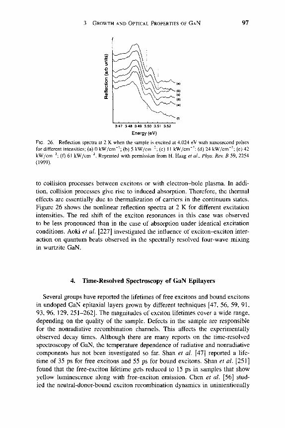
3 GROWTH AND OPTICAL PROPERTIES OF GAN 97
3.47 3.48 3.49 3.50 3.51 3.52
Energy (eV)
FIG. 26. Reflection spectra at 2 K when the sample is excited at 4.024 eV with nanosecond pulses for different intensities; (a) 0 kW/cm"^ (b) 5 kW/cm'^ (c) 11 kW/cm-^ (d) 24 kW/cm"'; (e) 42 kW/cm~^ (f) 61 kW/cm~^ Reprinted with permission from H. Haag et al., Phys. Rev. B 59, 2254 (1999).
to collision processes between excitons or with electron-hole plasma. In addi-tion, collision processes give rise to induced absorption. Therefore, the thermal effects are essentially due to thermalization of carriers in the continuum states. Figure 26 shows the nonlinear reflection spectra at 2 K for different excitation intensities. The red shift of the exciton resonances in this case was observed to be less pronounced than in the case of absorption under identical excitation conditions. Aoki et al [227] investigated the influence of exciton-exciton inter-action on quantum beats observed in the spectrally resolved four-wave mixing in wurtzite GaN.
4. Time-Resolved Spectroscopy of GaN Epilayers
Several groups have reported the lifetimes of free excitons and bound excitons in undoped GaN epitaxial layers grown by different techniques [47, 56, 59, 91, 93, 96, 129, 251-262]. The magnitudes of exciton lifetimes cover a wide range, depending on the quality of the sample. Defects in the sample are responsible for the nonradiative recombination channels. This affects the experimentally observed decay times. Although there are many reports on the time-resolved spectroscopy of GaN, the temperature dependence of radiative and nonradiative components has not been investigated so far. Shan et al. [47] reported a life-time of 35 ps for free excitons and 55 ps for bound excitons. Shan et al [251] found that the free-exciton lifetime gets reduced to 15 ps in samples that show yellow luminescence along with free-exciton emission. Chen et al. [56] stud-ied the neutral-donor-bound exciton recombination dynamics in unintentionally

98 ANNAMRAJU KASI VISWANATH
doped n-type GaN epilayers. At low temperature, the lifetime of bound excitons was estimated as 100 ps. The decreasing value of r with increasing tempera-ture was attributed to an increased rate of nonradiative recombination at higher temperatures. Kawakami et al. [253] estimated the biexciton lifetime as 39 ps. Pau et al. [255] performed time- and spectrally resolved femtosecond excita-tion correlation (FEC) experiments on hexagonal GaN at 10 K. This technique is also called population mixing [263, 264] and has been used to study tun-neling dynamics [265, 266], recombination lifetimes of excitons, [267, 268], hot carriers [269-271], and carrier sweepout time under applied field [272]. Figure 27 shows the FEC signal for different detection energies and different excitation powers for the DX exciton and A exciton energies as a function of time delay. The interpretation of these results is very complicated. Various dynamical events, such as the population buildup of the A exciton due to satura-tion in the formation of donor-bound excitons and the bimolecular formation of excitons from electron-hole pairs must be considered. The free-exciton signal S^{8) decays to zero in two time scales. The first time scale is the recovery time of the saturated DX population; the second time scale is equal roughly to the A exciton Hfetime. The donor-bound exciton signal ^^xCS) is negative at 5 = 0 and is caused by saturation of the DX population and a subsequent conversion of the DX population to free excitons by scattering from carriers generated by the second pulse. S^y^{8) decreases further up to 5 = 50 ps, which is attributed to the recovery time of the DX population, and finally approaches zero. For the A exciton and the donor-bound exciton DX, the reported lifetimes were 66 and 136 ps, respectively.
150 200 0 .0 100 150 200
Delay. 6 (ps) 50 100
HO.O
200
FIG. 27. (a) FEC signal for different detection energies and FEC signal for different excitation powers at (b) the DX exciton, and (c) the A exciton energies as a function of time delay. Reprinted with permission from S. Pau et al, Phys. Rev. B 58, 12, 916 (1998).

3 GROWTH AND OPTICAL PROPERTIES OF GAN 99
Im et al. [254] performed picosecond time-resolved photoluminescence of GaN epilayers grown on sapphire up to room temperature. At low temperatures, the decay was found to be dominated by trapping processes at low excitation levels. The radiative lifetime was dominated by free excitons up to 150 K. At higher temperatures, excitons were found to dissociate. The radiative recom-bination coefficient was estimated. Jiang and co-workers [91, 93, 96] investi-gated the dynamics in MBE grown samples. Pau et al. [256] noticed that the strain caused by the lattice mismatch between the sapphire substrate and GaN had a large influence on the population decay of free excitons in MBE grown GaN epilayers. Godlewski et al. [257] studied the GaN layers grown on Si by gas source MBE and explained their results by considering the tunnehng of excitons between bound and free excitons. Bound-exciton dynamics in GaN on SiC substrate were reported by Eckey et al. [258]. The impact of exciton dif-fusion on the optical properties of GaN layers grown on SiC was examined by Brandt et al. [259].
5. p-GaN
Light-emitting diodes and semiconductor lasers based on GaN were not pos-sible for a long time because p doping was not possible. For this reason, the first LEDs made of GaN were not the usual p-n junctions, but were based on the metal-insulator-semiconductor structure [273-279]. Pankove and co-workers [273-277] fabricated various GaN LEDs with red, yellow, blue, and violet color emission. These devices required very high operating voltages and hence they were not useful in practical devices. Several acceptor impurities were tried [280-292] to make p-GaN with Zn, Cd, Be, Mg, Hg, and Li. All these impu-rities were observed effectively to compensate the electrons in GaN, leading to highly resistive material.
A major breakthrough was made by Amano, Akasaki, and their co-workers [35, 293], who achieved p-GaN by low energy electron beam irradiation (LEEBI) of Mg-doped GaN. They also demonstrated the p-n junction LED by using LEEBI treated Mg-doped GaN as the p-type material. Later Nakamura et al. [20] also successfully obtained p-type GaN by thermal annealing. They also suggested [294] the hole compensation mechanism in p-type GaN. Mg was recognized as the most suitable acceptor impurity and Mg-doped GaN was grown by several workers using MOCVD [295-315] and MBE [316-332] techniques to study the variety of properties. In general, MOCVD growth has yielded better quality Mg-doped GaN than the poorer quality MBE grown sam-ples. However, MBE grown epilayers did not require LEEBI or thermal anneal-ing treatment to make p-type material. In addition to Mg, C [333] and Be [334] were doped in GaN by MOCVD and MBE techniques, respectively, and p-type conduction was reported. Ion implantation techniques initially were tried by Pankove and Hutchby [335], who implanted a long list of 35 elements in GaN.
100 ANNAMRAJU KASI VISWANATH
Apparently they could not obtain p-type material and several midgap states were generated during the damage-annealing treatment. More recently, Be, C, Mg, Zn, and Ca [336-342 ] have been implanted in GaN and p-type material could be achieved, p-type GaN has several important applications in fabricating opto-electronic semiconductor devices.
After successful demonstrations by Amano, Akasaki, and co-workers and Nakamura et al. [343], several groups around the world [296, 299, 302, 324, 327, 344-347] fabricated p-n junction light-emitting diodes in which Mg-doped GaN was used as the p-type layer. In these works, many attempts were also made to achieve optimum design for vertical cavity surface-emitting lasers and separate confinement heterostructure edge-emitting lasers. The stimulated emis-sion was observed only in optical pumping experiments. Nakamura et al. [26] made a remarkable improvement in fabricating an InGaN multiple quantum well structure semiconductor laser by current injection in which Mg-doped GaN was used as the light guiding layers, p-type Mg-doped GaN was also used to fabricate visible-blind ultraviolet photodetectors [348, 349], which are critical components in many applications such as flame sensors, ballistic missile warn-ing, UV astronomy, and space-to-space communications. The p-n junction made with p-type GaN is also important as a building block for unipolar devices such as field effect transistors [350].
Though many semiconductor devices based on GaN were made and put into commercial applications, most of the work has been largely based on trial and error. Many fundamental questions still remain to be solved. The important aspects to be understood are defects and doping properties of epilayers. It is also necessary to improve the quality of p-type GaN layers, which should not contain very deep levels. Very deep levels give rise to persistent photoconduc-tivity (PPC) [300, 329] which has detrimental effects on many photonic devices such as UV photodetectors. The PPC is also responsible for the current collapse sometimes observed in GaN-based field effect transistor [351, 352]. Very high-quality p-type GaN with low compensation and high mobilities is very impor-tant to realize continuous-wave operation of the semiconductor lasers through the reduction of contact resistance and threshold current [26, 353]. McGill and co-workers [354] have proposed novel heterojunctions of the type p-GaN/n-ZnSe, p-GaN/n-ZnS, and p-GaN/n-ZnO that facilitate minority carrier injection into other wide-bandgap semiconductors in which p-type doping is difficult or impossible to achive. They have also proposed p-GaN as a possible ohmic con-tacting layer to p-ZnSe or p-AlP. They later demonstrated [355] the fabrication of n-ZnS/p-GaN and injection of holes from p-GaN into n-ZnS, which is a very promising material for a new type of multicolor electroluminescent display technology.
Viswanath et al [356] investigated the detailed photoluminescence studies of magnesium-doped GaN epitaxial layers grown by metal-organic chemical vapor deposition on sapphire substrates. Energy levels of these acceptors were investi-gated by systematic photoluminescence measurements in the temperature range

3 GROWTH AND OPTICAL PROPERTIES OF GAN 101
of 12-300 K. Magnesium concentration was varied from <1 x 10 ^ to higher than 5 x 10 ^ cm~^. Photoluminescence measurements were made on the as-grown and annealed samples. Figures 28-31 show the PL spectra for different Mg concentrations and for different annealing conditions. In the 12-K spectrum shown in Figure 28a, a strong line at 3.276 eV and satellites on the low energy side at 3.184 and 3.092 eV were observed. The main line at 3.276 eV was attributed to zero-phonon donor-acceptor pair transition. The separation between two consecutive lines is about 92 meV. In the Raman spectra of undoped and Mg-doped GaN, transitions due to the LO phonons with an energy of 91 meV were observed. By this argument, the first satellite at 3.184 eV was assigned as the first phonon replica, and the line at 3.092 eV as the second phonon replica of the donor-acceptor pair transition. The donors may be nitrogen vacancies. From the equation given by Hopfield et al. [357] for the dependence of the recombination energy on the pair separation r, the binding energy of the accep-tor was estimated as 209 meV by using the previously determined values [61] of Eg = 3.505 eV and donor binding energy of 35 meV, and assuming a value of 15 meV for the Coulomb energy [282]. Figure 28b shows the PL spectrum in the excitonic region at 12 K for the as-grown Mg-doped GaN with [Mg] less than 1 x 10 ^ cm"^. FX(A) is the free exciton A, FX(B) is the free exci-ton B, DX is the donor-bound exciton, and AX is the acceptor-bound-exciton transition. PL peak positions and their assignments for Mg-doped GaN reported by Viswanath et al. [356] are given in Table VIII. The spectrum for the doped samples shown in Figure 28b has exactly the same features as those found in undoped GaN [61]. Figure 29 shows PL spectra at certain selected tempera-tures for the annealed samples of Mg-doped GaN with [Mg] <1 x 10 ^ cm~^. The DA pair transitions observed at low temperatures almost vanish at 120 K and a new broad peak was seen at around 2.94 eV, which was attributed to conduction-band electron transition to the Mg acceptor.
Figure 30 shows the PL spectra at various temperatures for doping levels of [Mg] = 1-5 x 10 ^ cm"^ In the 12-K spectrum, a strong peak at 3.256 eV and weak shoulders at 3.166 and 3.076 eV were detected. The main peak was attributed to donor-acceptor transition and the satellites were attributed to one-and two-phonon-assisted DA pair transitions. As the temperature is increased, this peak is quenched easily as expected for the DA pair transition. Also, this peak moved to a higher energy by a few millielectronvolts as in the case of Mg-doped GaN with [Mg] < 1 x 10 ^ cm~^ These assignments were also supported by time-resolved laser experiments. With an increase in the excitation power of the nanosecond Nd:YAG laser, the peak shifts to higher energy. The lifetime was found to be in the range of several microseconds, which is typical for donor-acceptor pair transitions. Considering these arguments, the possibility of this transition as band to acceptor was ruled out.
In Figure 31a, the PL spectrum at 12 K for the annealed GaN doped with [Mg] in the range of 1-5 x 10 ^ cm"^ is shown. In the annealed samples, the PL intensity was increased to a great extent. This was explained by considering

102 ANNAMRAJU KASI VISWANATH
c 5>
CL
p G«N
Mg < IxlO^'cm
DAP
2.6
Photon energy (eV) (a)
335 340 345 3.50 3 55
photon energy (eV)
(b)
FIG. 28. (a) Photoluminescence spectra at selected temperatures for Mg-doped GaN. The magne-sium concentration is less than 1 x 10'^ cm"\ DAP is the zero-phonon donor-acceptor pair tran-sition. DAP-ILO and DAP-2L0 are the first and second phonon replicas, (b) Exciton region PL spectrum at 12 K. Reprinted with permission from A. K. Viswanath et al., J. Appl. Phys. 83, 2272 (1998).
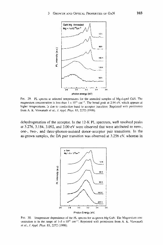
3 GROWTH AND OPTICAL PROPERTIES OF GAN 103
GaN:Mg Annealed
Mg<1x10^'cm
photon energy (eV)
FIG. 29. PL spectra at selected temperatures for the annealed samples of Mg-doped GaN. The magnesium concentration is less than 1 x 10 ^ cm"^ The broad peak at 2.94 eV, which appears at higher temperatures, is due to conduction band to acceptor transition. Reprinted with permission from A. K. Viswanath et ai, J. Appl. Phys. 83, 2272 (1998).
dehydrogenation of the acceptor. In the 12-K PL spectrum, well resolved peaks at 3.276, 3.184, 3.092, and 3.00 eV were observed that were attributed to zero-, one-, two-, and three-phonon-assisted donor-acceptor pair transitions. In the as-grown samples, the DA pair transition was observed at 3.256 eV, whereas in
2 8 3 0 3 2 3 4 3 6
Photon Energy (eV)
FIG. 30. Temperature dependence of the PL spectra for as-grown Mg:GaN. The Magnesium con-centration is in the range of 1-5 x 10 ^ cm~\ Reprinted with permission from A. K. Viswanath et ai, 7. AppL Phys. 83, 2272 (1998).

104 ANNAMRAJU KASI VISWANATH
p GaN Annealed
Mg 1-5x 10"cm^
DAP
DAP - 3L0
DAP -4L0 /
1 /
• 1 i L..
DAP cA
21.0 /
1 /
DAP J 1
1L0 A
* /
1 . 1 1
2 8 3 0 3 2
Photon Energy (eV)
(a)
p GaN Annealed
12K
60 K
9QK
140 K
220 K
300 K
3 4 36 3 0 3 2
photon energy (eV) (b)
FIG. 31. PL spectrum at 12 K for the annealed GaN doped with magnesium. The magnesium concentration is in the range of 1-5 x 10'^ cm~^ The zero-phonon and various phonon-assisted donor-acceptor pair transitions can be seen. The eA denotes the conduction band to the Mg accep-tor transition that overlaps the first phonon replica of the DA transition, (b) Temperature varia-tion of the photoluminescence of GaN:Mg epilayers that are annealed. The Mg concentration is 1-5 X 10 ^ cm~^. Reprinted with permission from A. K. Viswanath et al., J. Appl. Phys. 83, 2272 (1998).

3 GROWTH AND OPTICAL PROPERTIES OF GAN 105
TABLE VIII
PL PEAK POSITIONS AND THEIR ASSIGNMENTS FOR MG-DOPED GAN
Mg concn. (cm-3) Form
Temperature Peak position (K) (eV)
Assignment
<1 X 10'^ AS grown
5 X 10 ^ AS grown
Annealed
12
Annealed 12
180
1-5 X 10 ^ As grown 12
260
Annealed 12
12 220 300
12 140 300
12
300
3.276
3.184 3.092
3.276 3.184 3.092 2.94
3.256 3.166 3.076 3.181 2.900
3.276 3.184 3.092 3.000 2.908 3.184 2.916 2.878
3.184 2.900 2.800 3.276 3.190 2.900
Donor-acceptor zero phonon DAP-ILO DAP-2L0
DAP DAP-ILO DAP-2L0 Band to acceptor
DAP DAP-ILO DAP-2L0 Band to acceptor Band to acceptor
DAP DAP-ILO DAP-2L0 DAP-3L0 DAP-4L0 Band to acceptor Band to acceptor Band to acceptor
Band to acceptor Band to acceptor Band to acceptor DAP Band to acceptor Band to acceptor
Source: A. K. Viswanath et al., J. AppL Phys. 83, 2272 (1998).
the annealed sample it was at 3.276 eV. The shift of the peak to higher energy was explained by the increased p doping after annealing.
The PL spectra at different temperatures for the annealed samples are shown in Figure 31b. With an increase in temperature, the DA pair transition is ther-mally quenched and also moves to a higher energy by a few millielectronvolts as observed in other samples. In higher-temperature spectra, the peak at 2.9 eV was attributed to a deep acceptor level of Mg.
We discuss very briefly the transitions reported by various workers in dif-ferent samples of GaN doped with acceptors. Very deep level transitions have been reported [304, 308, 311] in the deep level transient spectroscopy (DLTS)

106 ANNAMRAJU KASI VISWANATH
measurements at 1.0, 1.2, 1.8, and 2.2 eV and a peak at 2.2 eV in the PL spec-trum [311]. The deep levels were thought to be due to the formation of complex Mg centers [311] that are also electrically active. Furthermore they also cause the Fermi level to be pinned near the mid gap and make the material highly resistive. However, in samples of high quality such mid gap levels were not observed [356].
Ilegems and Dingle [281] also reported a number of acceptor levels in semi-insulating GaN. At 4.2 K, they observed a number of shallow acceptor levels and a very deep level at 2.41 eV. The dependence of the Mg concentration on luminescence was initially studied by Amano et al. [295]. They reported PL spectra of as-grown samples at only two temperatures: 4.2 K and room temper-ature. In low doped materials, they observed donor-acceptor pair transitions at low temperatures and a weak peak at 550 nm (2.25 eV) at room temperature. In the highly doped GaN, they observed a deep level at 2.95 eV at 4.2 K and a weak green emission as well. At room temperature, a blue emission at 2.7 eV and green emission were observed. Nakamura et al. [294] studied a number of Mg-doped samples at room temperature under various treatment conditions. In all their samples, which were both LEEBI treated and nitrogen annealed, they observed the blue peak at 2.75 eV (450 nm) at room temperature. Smith et al. [358] studied the PL of both MBE and MOCVD grown p-type GaN and found identical results irrespective of the crystal growth method. In highly doped samples, they observed a very shallow acceptor level at 3.21 eV below 150 K and a deep level at 2.95 eV above 150 K. Both transitions were attributed to band to acceptor. At room temperature, they observed a very deep level peak at 2.6 eV. Myoung et al. [325] obtained p-type GaN by MBE without any post-growth treatment. They observed a very shallow level at 3.25 eV and deep levels at 2.87 and 2.43 eV. The very deep level emission was attributed to complex Mg centers. Wei and Zunger [359] developed the theory of core electron relaxation to explain the relationship between the electronic configuration of the dopant ion and the acceptor energy levels in II-VI wide-bandgap semiconductors such as ZnS, ZnSe, CdS, and CdSe. The theory was extended by Strite [360] and found to be appHcable even to III-V GaN, which has strong hybridization between Ga 3d electrons and the upper- and lower-valance-band s and p levels. Accord-ing to this theory, if the impurity acceptor has d electrons, the acceptor levels become deeper because of the p-d repulsion. For this reason, it was conjectured that Zn, Cd, and Hg dopants, which have d electrons, always give compensated material and it is not possible to achieve p-type GaN even after annealing.
In the case of Zn doping in GaN, Monemar et al. [283, 284] and Boulon et al. [288] have done extensive PL measurements and observed four peaks at 2.87, 2.6, 2.2, and 1.8 eV, where the first peak was assigned to the Zn acceptor at the substitutional Ga, wheereas the other very deep levels were thought to be due to Zn at the substitutional sites of N. We believe that the very deep levels in Zn-doped GaN are not due to core relaxation effects, because abnormally deep levels have been observed in the PL of GaN doped with impurities that do not

3 GROWTH AND OPTICAL PROPERTIES OF GAN 107
760 800 840 880 920
MAGNETIC FIELD (mT)
FIG. 32. ODMR spectra obtained on emission less than 3.0 eV from Mg-doped GaN film with B oriented 30° from c. Three resonances are clearly observed. Reprinted with permission from E. R. Glaser et ai, Phys. Rev. B 51, 13,326 (1995).
have d electrons, for example, 2.2 eV for Be, [281, 287, 290], 2.15 eV for C [291], and 2.23 eV for Li [290, 292].
Glaser et al. [315] studied the PL and optically detected magnetic resonance (ODMR) of a number of undoped and Mg-doped GaN epilayers grown by MOCVD. Figures 32 and 33 show the ODMR spectra of Mg-doped GaN. Based on the detailed analysis, models have been proposed for the donor and acceptor levels in undoped and Mg-doped GaN. These are shown in Figures 34 and 35. The model shown in Figure 34 incorporates a two-stage process that involves three distinct states: the shallow and deep donor states and an effective-mass acceptor state revealed from the weak, phonon-resolved 3.27-eV PL band. The donor-acceptor pair transition is from a shallow donor to a shallow acceptor. The transition from the double-donor to the shallow acceptor gives rise to the commonly observed yellow emission at 2.2 eV. In highly Mg-doped samples, the transition around 3.0 eV was thought to be due to shallow donors to Mg-related acceptors and the deeper emission at 2.0 eV was assigned to deep donors to Mg acceptors as shown in Figure 35.
Several groups have reported [361-371] on the theoretical aspects of accep-tors in GaN. Neugebauer and Van de Walle [361-366] studied the electronic structure, atomic geometry, and formation energies of native defects in GaN using first-principles total-energy calculations. In p-type GaN, the nitrogen vacancy is a donor, whereas in n-type GaN, gallium vacancy acts as an acceptor. It was also shown that vacancies are important for compensation. Hydrogen was found to act as a donor (H" ) in p-type GaN and as an acceptor (H~) in n-type
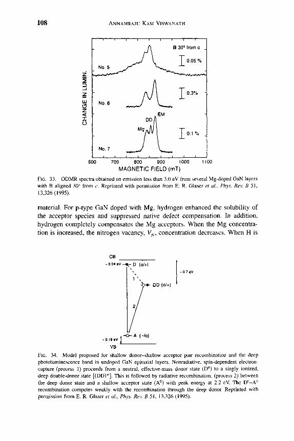
108 ANNAMRAJU KASI VISWANATH
z
111 o z < X o
• • 1 - I
' No. 5
k No. 6
h
^
No. 7
1 1 1
I r 1 T —
A / u EM
DDA
MgJ
1 1 1 1
- T T » • •
B 30° from c J
To.05%
T 0.3% -
*y
T 0.1 %
1 .JL.. . , ,J_
600 700 800 900 1000
MAGNETIC FIELD (ml) 1100
FIG. 33. ODMR spectra obtained on emission less than 3.0 eV from several Mg-doped GaN layers with B aligned 30° from c. Reprinted with permission from E. R. Glaser et al., Phys. Rev. 5 51, 13,326 (1995).
material. For p-type GaN doped with Mg, hydrogen enhanced the solubility of the acceptor species and suppressed native defect compensation. In addition, hydrogen completely compensates the Mg acceptors. When the Mg concentra-tion is increased, the nitrogen vacancy, Vj^, concentration decreases. When H is
DD (0/+)
FIG. 34. Model proposed for shallow donor-shallow acceptor pair recombination and the deep photoluminescence band in undoped GaN epitaxial layers. Nonradiative, spin-dependent electron-capture (process 1) proceeds from a neutral, effective-mass donor state (D^) to a singly ionized, deep double-donor state [(DD)+]. This is followed by radiative recombination, (process 2) between the deep donor state and a shallow acceptor state (A^) with peak energy at 2.2 eV. The D^-A° recombination competes weakly with the recombination through the deep donor. Reprinted with permission from E. R. Glaser et al, Phys. Rev. B 51, 13,326 (1995).

3 GROWTH AND OPTICAL PROPERTIES OF GAN 109
CB
• 3.0 eV
Mg-rel. Ace. (-/o)-
D (0/+)
- • - DO (W++)
- 2.0 eV
- 0.5 eV
VB
FIG. 35. Model proposed for donor-acceptor recombination in highly Mg-doped GaN films. Two recombination pathways are revealed by the ODMR spectra studies. The emission around 3.0 eV is assigned to EM donors (D) recombining with Mg-related acceptors. The deeper emission (near 2.0 eV) is assigned to recombination between deep donors (DD) and Mg-related acceptors. Reprinted with permission from E. R. Glaser et al., Phys. Rev. B 51, 13,326 (1995).
present, an increase in the Fermi level decreases the formation energy for the Mg acceptor and increases the formation energy for V^. This results in lowering of the defect concentration and an increased acceptor concentration. This is why Mg-doped GaN grown at higher temperatures (above 1200 K) always is heavily compensated. The compensating centers are either N vacancies or hydrogen, if present. This reasoning also explains why p-type GaN can be achieved without any postgrowth treatment in MBE samples grown at somewhat lower temper-ature (below 1000 K) and requiring no H in the growth process. When H is present, the H concentration equals the Mg concentration. The H donors and Mg acceptors form electrically neutral complexes. For this reason, the activation of Mg needs postgrowth treatments. First, the dissociation of Mg-H complexes is necessary and is generally accomplished by annealing. The hydrogen atoms that are released from Mg acceptors need to be either removed to the surface or into the substrate or neutralized at extended defects.
The ability of H to terminate dangling bonds to passivate or compensate both shallow and deep defects is very well known in semiconductor technology [372]. The role of H in the passivation of the Mg acceptors was discussed by Van Vechten [371]. Neugebauer and Van de Walle [364] showed that the Mg-H com-plexes in GaN have entirely different atomic structure compared to other semi-conductors such as Si and GaAs. This happens due to the strong ionic nature of GaN and the large bond strength of the Ga-N bond. Van de Walle [365] discussed the behavior of hydrogenated nitrogen vacancies during annealing of acceptor-doped GaN and proposed a correlation with the frequendy observed luminescence band around 420 mm. Neugebauer and Van de Walle [366] more recently reported the results of a comprehensive first-principles investigation of several possible acceptors in GaN. They found that Mg is still the best acceptor and better than Li, Na, K, Be, Zn, and Ca. Two factors were considered: first, the

110 ANNAMRAJU KASI VISWANATH
strength of the chemical bond between the acceptor and its neighbors; second, the atomic size match between the acceptor and the host atom that it substitutes. It was pointed out that Be doping may have compensation problems due to interstitial donors, although it is a good candidate. Boguslawski et al. [367] concluded that due to the wide bandgap of nitrides, self-compensation effects strongly reduce both n- and p-type doping efficiencies due to the formation of gallium vacancies and interstial Ga, respectively. They also studied [368, 369] the amphoteric properties of substitutional C, Si, and Ge in GaN. When Si and Ge substitute for cations, they are shallow donors in GaN. On the other hand, they will be deep acceptors if they occupy the N site. The doping efficiency of all these impurities is very low due to the self-compensation problem that occurs due to the occupation of both cations and anions in the lattice by the impurity ion. The acceptor binding energies of Be, Mg, Zn, Ca, C, and Si in GaN were estimated by Mireles and Ulloa [370]. The atomic origin of the deep levels in p-GaN was studied by Chadi [373] from first-principles calculations. He attributed the deep levels to Ga vacancies above the valence-band maximum.
Several groups investigated [374-390] acceptor-doped GaN, in particular Mg doping, and gave different interpretations for the electronic structure and pho-toluminescence of p-type GaN.
6. n-GaN
One of the important problems still to be solved in GaN technology is control of background impurities and defects. The undoped GaN grown by different methods has n-type conductivity and the carrier concentration is in the range of 10^^-10^^ cm~^. The number of carriers and defects depends on the growth technique, growth parameters, substrate, buffer layer, treatment methods, and so forth. If the background carrier concentration is high, then it leads to a degenerate semiconductor. This is a serious problem when p-n junctions and semiconductor lasers have to be constructed. Identification of the background impurities and defects that give rise to the conductivity of undoped samples has not been confirmed so far. The energy levels and electronic structure associated with these defects and impurities, which may be donors or acceptors, is currently a hot topic.
Maruska and Tietjen [391] and Ilegems and Montgomery [392] initially pro-posed that native defects were responsible for high carrier concentrations. Nitro-gen vacancy [391-397] and oxygen impurities [398, 399] were considered as background donors. The residual donors and acceptors in GaN were investigated by theoretical calculations [361-369, 400-405], electron spin resonance spec-troscopy [406-409], optically detected magnetic resonance [407^13], Over-hauser shift magnetic double resonance [414], Zeeman spectroscopy [415], infrared reflectivity [416], optical absorption and transmission [417], Fourier

3 GROWTH AND OPTICAL PROPERTIES OF GAN 111
transform infrared absorption spectoscopy [418], and Hall effect measurements [419-424].
Viswanath et al. [64] performed detailed photoluminescence studies of shal-low donors in GaN. Ionized donor-bound excitons were observed very clearly in addition to donor bound excitons (Fig. 36). They estimated the donor bind-ing energy as 35 meV. From Hall effect measurements on Si-doped GaN, the activation energy of the shallow donor was reported [425] as 27 meV. Hacke et al. [426] gave a value of 27 meV for donors in Si-doped GaN grown by metal organic vapour phase epitaxy (MOVPE) using silane. From luminescence experiments, Gotz et al. [420], evaluated the Si donor binding energy as 22 meV by observation of donor-aceptor transitions and another unidentified shallow donor with a binding energy of 34 meV. In Zeeman spectroscopy [415], donors with binding energies of 31.1 and 33.8 meV were observed. Lagerstedt and Monemar [282] experimentally determined a value of 29 meV for the donor binding energy by observing free-to-bound and donor-acceptor pair transitions. A comparison of binding energies of shallow donors in GaN estimated by dif-ferent methods is given in Table IX.
Figure 37 shows the temperature dependence of the full width at half-maximum (FWHM) of the neutral-donor-bound exciton PL peak reported by Viswanath et al. [64]. The solid squares represent the experimental points and the straight line denotes the linear fit of the experimental points. The
undoped GaN 9K
3.425 3.450 3.475 3.500 3.525
photon energy (eV)
FIG. 36. Luminescence spectrum of GaN epilayer at 9 K. Dotted lines show the deconvolution into Lorentzian fitting of various transitions. The dashed fine is the Lorentzian fitting of the experimental spectrum. The inset shows the temperature dependence of the transition energies of free excitons A and B. D+X is due to ionized donor-bound exciton transition. Reprinted with permission from A. K. Viswanath et al., Phys. Rev. B 58, 16,333 (1998).

112 ANNAMRAJU KASI VISWANATH
TABLE IX
BINDING ENERGIES OF SHALLOW DONORS IN GAN ESTIMATED BY
DIFFERENT METHODS
Estimation method
Photoluminescence of donor-bound exciton
Zeeman spectroscopy
Fourier transform infrared spectroscopy
Photoluminescence
Electron cyclotron resonance spectroscopy
Hall effect measurements
Photoluminescence
Binding energy (meV)
35
31.1 33.8 35.5
22 34 31.7
27 27 29
Type of donor
Residual
Residual Residual Residual
Silicon Residual Residual
Silicon Silicon Residual
Ref.
64
415 415 418
420 420
36
425 426 282
Source: A.K. Viswanath et al, Appl Phys. A 67, 551 (1998).
undoped GaN Donor bound exciton
0 20 40 60 80 100 120
Temperature (K)
FIG. 37. Variation of FWHM as a function of temperature for the neutral donor-bound exciton PL peak. The squares are experimental line widths. The straight line is a linear fit of the experimental line widths considering acoustic-phonon scattering. Reprinted with permission from A. K. Viswanath et al, Appl Phys. A 67, 551 (1998).

3 GROWTH AND OPTICAL PROPERTIES OF GAN 113
• 10
c
undoped GaN Donor bound excitoni
0.00 0.2 i 0.08 0.12 0
1/T(Ki)
FIG. 38. Activation energy plot of the PL intensities of the neutral donor-bound excitons vs. \/T. The slope of the straight line gives the thermal activation energy of neutral donor-bound excitons as 9 meV. Reprinted with permission from A. K. Viswanath et ai, Appl Phys. A 67, 551 (1998).
experimental line widths may be described by
r(r)(FWHM) = ro + 7phr (3)
Here T{T) is the line width at temperature T, FQ is the low-temperature limit of the line width and contains the contributions due to collision with other exci-tons, scattering by the crystal imperfections, or radiative recombination, and Yph is a measure of the exciton-acoustic-phonon coupling strength. The linear increase of the line width with temperature shows that only acoustic phonons contribute to the homogeneous broadening. Whereas an exponential increase is not observed in the line-width variation as a function of temperature, it is con-cluded that the longitudinal optical phonons do not participate in the broadening mechanism. The hnear fit yielded FQ = 1.55 meV and y^^ = 0.14 meV/K.
The integrated emission intensity of the neutral-donor-bound exciton as a function of l/T is shown in Figure 38. The solid squares denote the experi-mentally deduced intensities. From the slope of the straight line, the activation energy was estimated as 9 meV. This represents the binding energy of the exci-ton to the neutral donor. This value agrees very well with the value obtained from the 9-K PL spectrum, which is 7 meV.
Figure 39 shows the ratio of total intensity of free excitons to the total inten-sity of bound excitons, which includes both neutral and ionized donors, as a function of temperature. With an increase in temperature, the intensity ratio increases. This shows that the bound excitons dissociate thermally, releasing

114 ANNAMRAJU KASI VISWANATH
40 60 80
Temperature (K)
FIG. 39. The ratio of total intensity of free excitons (A and B) to total intensity of bound excitons (neutral and ionized donor), /FE/^BE' ^S a function of temperature. Reprinted with permission from A. K. Viswanath et ai, AppL Phys. A 67, 551 (1998).
free excitons and neutral donors as well as ionized donors. At 100 K, the inten-sity ratio drastically shoots up. The donor-bound excitons, which are the only bound excitons that exist at this temperature, completely dissociate and form free excitons and neutral donors. This temperature corresponds to the dissoci-ation energy of the donor-bound exciton which turns out to be 9 meV in the energy scale. This energy value is in excellent agreement with the localization energy of 7 meV observed in the PL spectrum and the activation energy of 9 meV deduced from the PL intensity plot as a function of l /T.
Contactless electroreflectance at room temperature was used [427] to eval-uate band bending at the surface of epitaxial n-type GaN/sapphire. Persis-tent photoconductivity was observed [428, 429], even in undoped n-type GaN. Correspondence between the E2 deep level {E^ — 0.55 eV) in n-type GaN and photoionization was made by optical techniques [430]. The diffusion of O and H in unintentionally doped n-type GaN was investigated [431] using cathodo-luminescence kinetics and imaging at 4 and 300 K by wavelength dispersive X-ray analysis. A similarity was found between the 0.88-eV photoluminescence in GaN and O^ donor emission in GaP in the optical investigations made by Chen et al. [432]. In very elegant experiments, Buyanova et al. [433] investi-gated the zero-phonon and phonon-assisted raditive recombination of free exci-tons in n-GaN using the polariton approach [434-437]. Excitonic properties of the wide-bandgap semiconductors with dipole-allowed direct band-to-band recombinations can be described by considering the polariton concept. In the polariton picture, the strong coupling between exciton and photon is considered. This coupling results in a mixed-mode excitation called exciton-polariton with

3 GROWTH AND OPTICAL PROPERTIES OF GAN 115
25
1 20
15
S i o UJ
-
-
-
L
h
1 ^
' n-typ« GaN
7,lo'®cm"3/
3«10|®cnr3^
a^ro^W;^/ 5 i . l 0 ^ ' c m " ^
, .2 3.3
1
Ij7_j \
/ L*l\
3.4
1
'
35 §V
— 1 — - — »" ••"T 1
n-typ« GaN 1 Aib*7x10'*cfn-'
r=293K
1
/ ^ , . .
2.0 2.5 3.0 ENERGY /»v (eV)
3.5
FIG. 40. Room-temperature photoluminescence spectrum of n-type GaN at an excitation intensity of 3 W/cm^. The inset shows the near-band-edge transition for n-type GaN doped with different Si concentrations. Reprinted with permission from E. F. Schubert et al., Appl. Phys. Lett. 71, 921 (1997).
a two-branch dispersion curve in K space. The spUtting between these branches is a measure of the coupHng strength. Exciton-polaritons have been studied in CdS [436, 437], CdSe [437] and GaAs [438]. Based on the observation of very unusual intensity dependence of free exciton PL and its phonon replicas, Buyanova et al. [433] suggested that there is a strong impurity scattering of exciton-polaritons.
Stress relaxation in Si-doped GaN grown by MOCVD was studied by Ruvimov et al. [439] using a number of techniques such as photoluminescence, Raman spectroscopy, transmission electron microscopy, and X-ray diffraction. They found that the layer quality improved when GaN was doped by Si to a concentration of 3 x 10 ^ cm~^ Look et al. [440] suggested multiple phonon hopping mediated conduction among deep centers based on the too small Hall coefficients observed in MBE grown n-GaN. Zolper et al. [441] imple-mented Si implantation in GaN and achieved 50% activation when the dose rate was 1 x 10 ^ cm~^. Schubert et al. [442] investigated the optical proper-ties of n-type GaN doped with Si. The concentration was varied from 5x10^^ to 7 X 10 ^ cm~^. As the concentration of Si increased, the PL line width of the near-bandgap optical transition increased from 47 to 78 meV. This find-ing was explained by considering the potential fluctuations caused by random distributions of donor impurities. The PL spectra are shown in Figure 40. A theoretical model was also developed by taking into consideration the poten-tial fluctuations that arise due to doping. In the entire range of doping con-centrations, the measured broadening was found to be in excellent agreement with calculated values as shown in Figure 41. Persistent photoconductivity was

116 ANNAMRAJU KASI VISWANATH
100
> £ 80 U J <J
I
I 60
UJ
o CO UJ
z 1 3
n-type GaN r»293K • Experiment — Theory
Tolal broadening
10' 10" 10' 10" 10" IMPURITY CONCENTRATION NQ^N^ (cm" )
10^
FIG. 41. Experimental line widths of the near-band-edge transition of n-type GaN as a function of the doping concentration. Also shown is the theoretical thermal broadening and broadening due to random impurity concentration fluctuations. Reprinted with permission from J. C. Zolper et al., Appl Phys. Lett. 70, 2729 (1997).
reported by Beadie et al. [443] in Si-doped n-GaN. The broadening mecha-nism of the near-bandgap photoluminescence in n-type Si-doped GaN was stud-ied by Ilipoulos et al. [444]. An impurity band-broadening model was used to explain the experimental line widths. Fang et al. [445] reported the results of DLTS on n-type GaN. Zhang et al. [446] measured the photoreflectance of Si-doped n-GaN films grown by MOCVD. The energy positions of near-band-edge transitions for different Si concentrations were determined using a theoretical curve fitting procedure. Razeghi's group [447] observed bandgap narrowing in Si-doped GaN. The PL peak positions of heavily compensated samples were red shifted compared to moderately compensated samples and the red shift was very large for higher electron density (Fig. 42). Figure 43 shows clearly the bandgap narrowing effect. The results are interpreted by considering the band-edge potential fluctuations that arise due to inhomogeneous residual impurities. Zaldivar et al. [448] investigated the cathodoluminescence of GaN:Si films. They observed that the round hillocks and nanopipes have no influence on the photoluminescence properties of the film. Oh et al. [449] correlated the optical properties with the transport properties of GaN:Si. The band-edge PL was found to vary in intensity and energy depending upon the mobility. This variance was attributed to potential fluctuations associated with inhomogeneous impurities or local defects that, in turn, lead to space-charge scattering of carriers and red shift of the PL fine. Strain relaxation was also explained from experimental observa-tions. Joshkin et al. [450] observed fine structure in the photoluminescence of He"^-irradiated GaN. The results were compared with GaN doped with oxygen.

3 GROWTH AND OPTICAL PROPERTIES OF GAN 117
(A c 0) c
T=293 K GaN:Si
3.2 3.3 3.4 35 36
M2. n=1.6x10"cm"*
H3. n=1.4x10"cm'*
- i I I L. 1.9 2.1 2.3 2.5 2.7 2.9 3.1 3.3 3.5 3.7
Energy (eV)
FIG. 42. Typical PL spectra of two representative samples from each sample set. The inset shows a gradual red shift of band-edge emission with increasing carrier density. Reprinted with permission from I. H. Lee et al, Appl. Phys. Lett. 74, 102 (1999).
GaN epitaxial layers that have a large number of defects exhibit a very broad luminescence centered around 2.2 eV that is commonly called yellow lumi-nescence [287, 291]. Pankove et al. [287], who observed the yellow band in ion-implanted samples, attributed it to deep states that may arise in the ion implantation process. The broad yellow luminescence was interpreted [291] as
C 3.41 .2
(0
3.39
3.38
I ' I D
^ ^ \ ^
h V
1 N# Slope«-2.1x10''eVcnr^
1 , i_ . ^ . 1
a
1 T f r • —
• SetM • SetH
J J
J
D\ ^^ 1
° \ D J Slop«=-1.3x10^ eV c m N
^
1 ... __j ._
00 5.0x10* 1.0x10' 1.5x10* 2.0x10* 2.5x10*
1/3. - 1 .
n (cm ) FIG. 43. Peak positions of the UV transition as a function of «'/^, showing clear bandgap narrow-ing effect. The solid lines are from the least squares fit. Reprinted with permission from L H. Lee et al, Appl Phys. Lett. 74, 102 (1999).

118 ANNAMRAJU KASI VISWANATH
due to band to electron transition from the conduction band to a band of deep acceptor states placed 860 meV above the valence band. The acceptor states were thought to be due to carbon impurities. Singh et al. [451] reported the intensity dependence of bandgap and yellow luminescence in GaN films grown by MBE. They observed that the bandgap luminescence is linearly dependent, whereas the yellow luminescence has a nonlinear dependence on the incident intensity. These data were compared with a recombination model in which a density of recombination centers 2.2 eV below the conduction-band edge was assumed. Hofmann et al. [452] attributed the yellow luminescence to a tran-sition from a shallow donor to a double donor, as shown in Figure 44. The model proposed by Glaser et al. [315], which was discussed in the previous sections, is also given in Figure 44, for comparison purposes. According to Glaser et al. [315], the yellow luminescence originates from a recombination between a deep double donor and a shallow acceptor. The electron transfer from the shallow donor to the deep donor state occurs through a spin-dependent nonradiative transition. Hofmann et al. [452] made their conclusions from the observation of very small activation energy of 15 meV deduced from the temperature-dependent PL studies, shown in Figure 45, and the nonexponential decay of the luminescence in the time-resolved experiments, shown in Figure 46. Moustakas's group [417, 453] examined the pressure dependence of the yel-low luminescence in bulk crystals and epitaxial layers of GaN. A blue shift of 30 lb 2 meV/GPa was observed in the PL peak position for pressures up to about 20 GPa, whereas for higher pressures, saturation of the luminescence peak posi-tion was noted. Based on these results, the yellow luminescence was interpreted as due to recombination of electrons from shallow donors to a deep level state of donors or acceptors. Koschnick et al. [454] suggested that Ga interstitials are residual donors based on their optically detected electron nuclear double
Model A Model B
-'sh D K w^Sm D I. MM^ *5P'" dependent" "nonradiative" recombination
• DD"*"
2.2 eV PL
- A .
2.2 eV PL
.(0) (or Acceptor)
sh
\ \ \ \ V V B : O-N/^ :VB-
FIG. 44. Sketches of the two recombination models under the discussion for the 2.2-eV emission in GaN. Model A [452]: Shallow donor (D^J to deep double donor (DD^) or deep acceptor (A) recombination. Model B [315]: Deep donor (DD^) to shallow acceptor recombination as obtained by Glaser et al.

3 GROWTH AND OPTICAL PROPERTIES OF GAN 119
c
05
i/i C 0)
E = I5me^
10O 150 200 250 300 350
Temperalure(K)
2.0 2.5 3.0 Energy (eV)
3.5
FIG. 45. Low-temperature photoluminescence spectrum of undoped GaN grown by metal-organic vapor phase epitaxy. The inset shows the intensity variation of the 2.2-eV emission as a function of temperature. Reprinted with permission from D. M. Hofmann et al, Phys. Rev. B 52, 16,702 (1995).
resonance (ODENDOR) experiments on the 2.2-eV yellow band in GaN thin films. The theoretical work of Neugebauer and Van de Walle [363] supports the involvement of a deep acceptor in yellow luminescence. The deep acceptor was thought to be due to gallium vacancies. The competition between bandgap and yellow luminescence, and its relevance for optoelectronic devices was exam-ined by Grieshaber et al. [455]. Microcavity effects were also observed [456] by the same group. Optical-isothermal capacitance transient spectroscopy was employed by Hacke and Okushi [457] to examine the mid-gap carrier traps in n-type Si-doped GaN grown by MOCVD. Liu et al. [458] speculated that the yellow luminescence is due to electron-hole recombination at positively charged Ga interstitials local to dislocations. Ramsteiner et al. [459] proposed
1x10 1x10 1x10 1x10
Time (sec)
FIG. 46. Photoluminescence decay time measurement on the 2.2-eV PL band in GaN. Calculated decay according to the shallow donor-deep donor model using Bohr radius of (a) 27 A and (b) 8 A, Reprinted with permission from D. M. Hofmann et al, Phys. Rev. B 52, 16,702 (1995).

120 ANNAMRAJU KASI VISWANATH
the involvement of shallow donors in yellow luminescence based on resonant Raman spectroscopy experiments. This assignment was later questioned by Siegle et al. [460], who also performed resonance Raman spectroscopy of GaN epilayers.
Schubert et al [461] employed photoluminescence techniques to study the dependence of yellow luminescence in n-type GaN on the doping concentration and concluded that the yellow luminescence is due to a compensating center. Reynolds et al. [462] observed similarities between the yellow luminescence in GaN and the green luminescence in ZnO. Chen et al. [463] investigated the yel-low luminescence in undoped n-type GaN and a set of Se-doped GaN epitaxial films by photoluminescence, Raman scattering, and photoconductivity. Yellow luminescence was thought to be due to a transition from the conduction-band edge to a deep acceptor. Se atoms at the N antisites were proposed as being responsible for the yellow emission. Persistent photoconductivity was observed after the yellow band excitation. Similarities were drawn between the N antisites in GaN and As antisites in GaAs. Calleja et al. [464] performed photocapaci-tance spectroscopy of GaN and proposed the existence of a deep trap at 1 eV above the valence band as the recombination path for the yellow luminescence.
Eisner et al. [465] performed local-density-functional calculations and found that a deep double acceptor, VQ^-ON, and a deep single acceptor, VQ3-(ON)2,
are involved in the yellow luminescence. The influence of surface morphol-ogy on the yellow luminescence was examined by Godlewski et al. [466] by cathodoluminescence measurements and they found that there is no connection between them. The dependence of the yellow luminescence on the slit width of the spectrometer was investigated by Tu et al. [467]. Reddy et al. [468] corre-lated persistent photoconductivity with yellow luminescence in h-GaN/sapphire and c-GaN/ GaAs SiC grown by MBE and concluded that the same defect is involved in both processes. Tu et al. [469] implemented depth profiling mea-surements of photoluminescence that revealed that the origin of yellow lumi-nescence is native defects instead of impurities. Rhee et al. [470] investigated temperature-dependent photoluminescence excitation spectroscopy on the yel-low band in GaN. They found evidence for the already known 205-meV accep-tor and another hitherto unknown level at '^120 meV, which may be due to an impurity or a defect. Glaser et al. [471] reported ODENDOR on several GaN epitaxial layers to search for effective-mass donor and deep-defect ODMR on the 2.2-eV emission. Li et al. [472] investigated the yellow luminescence by low-temperature photoluminescence and spatially resolved photoluminescence. They attributed the yellow luminescence to extended defects and native point defects.
Sun et al. [473] reported very interesting results on ultrafast electron dynam-ics in n-doped GaN (Fig. 47). They used multiple-wavelength pump-probe tech-niques. A fast electron cooling with a time constant of 500 fs was observed that shows that the electrons are the major carriers in cooling processes. Elec-trons in band-tail states were found to relax at the same rate as the conduction

3 GROWTH AND OPTICAL PROPERTIES OF GAN 121
t:
720/360 nm
725/362.5 nm
730/365 nm
x2 735/367.5 nm
x5 740/370 nm
T 2 3 4
Time Delay (ps)
FIG. 47. Measured transient transmission changes (solid lines) for pump-probe wavelengths of 720/360, 725/362.5, 730/365, 735/367.5, and 740/370 nm (from top to bottom). The experimental results are vertically displaced for clarity. Dotted lines on top of the results are the generated convolution fits. Reprinted with permission from C. K. Sun et al., Phys. Rev. B 59, 13,535 (1999).
electrons, indicating (<500 fs) carrier capture into shallow band-tail states and fast scattering between shallow band-tail electrons and conduction-band elec-trons. By varying the pump photon energy, conduction-band intervalley scat-tering of GaN was studied. By choosing the pump photon energy, the electron cooling behavior was found to be delayed by intervalley returned electrons with a time constant of 1 ps. The energy separation between the bottom of the U valley and the F valley conduction-band minimum in GaN was found to be 1.34 eV. Mair et al. [474] studied the time-resolved photoluminescence of ionized donor-bound excitons in GaN doped with both Mg and Si. The lifetime of the ionized donor-bound exciton was estimated to be 160 ps and is longer than the lifetime of the neutral-donor-bound exciton.
Optical Pumping and Lasing in GaN Epilayers and Heterostructures
Semiconductor lasers based on GaN were impossible for a long time because of the difficulties in making p-type GaN. Pankove et al. [273-277] were

122 ANNAMRAJU KASI VISWANATH
the first to fabricate a number of light-emitting diodes with metal-insulator-semiconductor structure. These LEDs gave a number of colors including red, yellow, blue, and violet. Hitachi also demonstrated [343] several LEDs that emit in green and yellow regions. The major drawback in these devices is the high operating voltages. The major milestone was reached by Amano, Akasaki, and co-workers [35, 293], who made p-type GaN by LEEBI treatment and also demonstrated p-n junction LEDs. However, Dingle et al. [475] were the first to report the optical gain of 1300 cm~^ in a GaN needle at 2 K with excitation power of 300 KW/cm^. Khan et al. [476] estimated an optical gain of 10" cm~^ in epitaxial GaN at room temperature. Amano and Akasaki's group demon-strated optically pumped edge-mode UV-stimulated emission from bulk GaN [477] and surface-mode UV-stimulated emission from AlGaN/GaN double het-erostructures [478] with low-threshold pumping power density at room temper-ature from GaN grown by using an AIN buffer layer. Kim et al. [479] reported an optical gain of 160 cm~^ at a pumping power density of 200 KW/cm^ for the optically pumped AlGaN/GaN double heterostructure. Figure 48 shows the configuration used for the optical pumping experiment and Figure 49 shows the dependence of emission intensity on excitation length for different pump pow-ers. Nakamura et al. [343] succeeded in making high-power GaN p-n junction blue light-emitting diodes in which they used a GaN buffer layer (Fig. 50). Figure 51 shows the output power of the p-n junction GaN LED as a function of current. The external quantum efficiency was as high as 0.18%. The output power was almost 10 times higher than that of the conventional SiC blue LEDs. The peak wavelength was in the violet region, at 430 nm.
Vaudo et al. [327] fabricated LEDs based on GaN p-n junctions grown by plasma-assisted MBE. The emission from LEDs could be shifted from the orange to the violet spectral region by changing the drive current. Razeghi's group [480] reported the observation of stimulated emission from Ge-doped
pulsed Nz laser 337.Inm 8nsec. 10Hz
AIGaN
FIG. 48. Schematic drawing of the AlGaN/GaN DH and the configuration for the measurement of optical gain. Reprinted with permission from S. T. Kim et al., Appl. Phys. Lett. 64, 1535 (1994).

3 GROWTH AND OPTICAL PROPERTIES OF GAN 123
TT 3
2h
AIGaN/GaN DH.
1 -y
y/ gains
a tR .T . ^
200kW/cm|YV, ^
160cm 120cm 34cm
^"^HOkW/cm^
^^-^^^rsrA 100k W/cm'
' (at 200kW/cm') (al MOkW/cm')
' (al lOOkW/cm^)
o. 1 4)
0 5 10 15 20 25
Excitation Length (x10Mm]
FIG. 49. Variation of integrateci emission intensity with exciton length at different optical pumping power densities. The gain g was deduced from a formula in the literature. Reprinted with permission from S. T. Kim et al, AppL Phys. Lett. 64, 1535 (1994).
GaN at room temperature. Under high excitation, red shift of the bandgap energy was observed and explained by considering the exchange energy of electron-electron, and hole-hole interactions. Redwing et al. [481] fabricated a GaN-based vertical cavity surface-emitting laser (VCSEL). A nitrogen laser was used for optical pumping along a cleaved sample edge and emission was observed at 363 nm (Fig. 52). The VCSEL structure consists of a 10-/xm GaN active layer that is sandwiched between 30-period Alo4oGao6oN-Alo i2Gao8gN Bragg reflectors. When the nitrogen pump intensity is more than 2.0 MW/cm^, stimulated emission occurs as shown in Figure 53. Kurai et al. [482] demon-strated optically pumped stimulated emission in homoepitaxial GaN for the first time. The lasing threshold of the pumping power density is 0.86 MW/cm^. Sun et al. [150] grew GaN films on cubic (111) MgAl204 substrates by low-pressure MOCVD. Stimulated emission was observed in these samples by opti-cal pumping. Tanaka et al. [483] investigated MOVPE selective growth of GaN layers on sapphire substrates for low-loss optical waveguide structures. They
P-Electrode
P-GaN Layer N-Electrode
N-GaN Layer
GaN Buffer Layer
Sapphire Substrate
FIG. 50. Structure of the p-n junction GaN LED. Reprinted with permission from A. A. Yamaguchi et al, Appl Phys. Lett. 71, 374 (1997).

124 ANNAMRAJU KASI VISWANATH
Fonvard Current IpCmA)
FIG. 51. Output power (P) of the p-n junction GaN LED and the conventional 8-mcd SiC LED as a function of forward current (/^). m is an exponent of 1^ when it is assumed that P is proportional to ip. Reprinted with permission from A. A. Yamaguchi et ai, Appl Phys. Lett. 71, 374 (1997).
obtained rectangular cross sections by controlling the nitridation of the sub-strate surface and the growth temperature. Stimulated emission was reported at 77 K. Lasing was achieved at threshold powers of about 0.05 MW/cm^. Song's group observed stimulated emission by optical pumping in GaN epilay-ers [484] and GaN/AlGaN separate confinement heterostructures (SCH) grown
GaN-AIGaN Vertical Cavity Surface Emitting Laser
Las«r I Emission
^ = A I G a N ReMQctof (2 .3 t im)==^
GaN Activ« (10^m)
AJGaN Reflector (2.3 M m ) ^ •«eaau!.!'>.iiyj];iH!«:'i-!Kw;a.«!na!!«iHg<j
I AIN Buffer (1 sol i) I
N Sapphire Substrate
FIG. 52. Schematic cross section of the VCSEL structure. The Bragg reflectors are 30-period Alo4o Gao6o N/AIQ 12 Gaogg N (397 A/372 A) multilayer stacks. Reprinted with permission from J. M. Redwing et al., Appl. Phys. Lett. 69, 1 (1996).

3 GROWTH AND OPTICAL PROPERTIES OF GAN 125
L =0.65g
h-n^Krri f i I I I I I 11 I I I I I" 355 360 365 370 375 380
FIG.
V/avelength (nm)
53. Room-temperature surface emission spectra for the GaN/AlGaN VCSEL structure obtained at pump intensities of 1.3 MW/cm (lower trace), 2.2 MW/cm (middle trace), and 2.6 MW/cm^ (upper trace). These intensities correspond to 0.657^ , 1.1/th and 1.3/th, respectively, with /,h = 2.0 MW/cm^. The broad GaN luminescence spectrum observed at lower powers is accom-panied by emergence of a laser mode at 363.5 nm near threshold. At powers well above threshold, additional modes emerge ~1.3 nm above and below the 363.5-nm line. Reprinted with permission from J. M. Redwing et al., Appl Phys. Lett. 69, 1 (1996).
by MBE [485]. In the SCH structure, lasing was observed at room tempera-ture for low-threshold pump powers of 90 KW/cm^. The maximum emission was at 361.5 nm. The optical pumping experiments were conducted using a frequency-tunable nanosecond Nd:YAG laser system with a side pumping con-figuration. The threshold pumping power is 1 order of magnitude less than that reported for GaN epilayers. This was thought to be due to carrier confinement and waveguiding effects in SCH. A cubic GaN/AlGaN heterostructure on GaAs substrate was fabricated by MOVPE under low V/III molar ratio conditions by Nakadaira and Tanaka [486]. Stimulated emission was observed from the cleaved edge by optical pumping. The peak wavelength was 387 nm and the threshold pump density was 2.4 MW/cm^.
A number of other research groups have reported [487-500] stimulated emis-sion in GaN-based materials. Onabe's group [495] achieved stimulated emis-sion from an optically pumped cubic GaN/AlGaN heterostructure grown on a GaAs (100) substrate. Their success paves the way for optoelectronic integration

126 ANNAMRAJU KASI VISWANATH
360 380 400 420 440 460
Wavelength ( nm)
FIG. 54. Edge emission spectra from a cubic GaN/AlGaN heterostructure with 0.8-mm-long cavity at 15 K under different pump power intensities: (a) 1 MW/cm^; (b) 3 MW/cm^; (c) 5 MW/cm^ (d) 9 MW/cml Reprinted with permission from J. Wu et aL, Appl. Phys. Lett. 73, 1931 (1998).
of GaN with the the well established III-V GaAs semiconductor technology. Figure 54 shows the edge emission spectra and lasing in a cubic GaN double heterostructure. In Figure 55, emission intensity as a function of pump power density is shown. Song and co-workers [497] observed lasing in GaN pyra-mids under strong optical pumping at room temperature. The pyramids were laterally overgrown on a patterned GaN/AlN seeding layer grown on a (111) silicon substrate by MOCVD. The pyramids were individually pumped, imaged, and spectrally analyzed through a high magnification telescope with the help of a high-density pulsed Nd:YAG laser. At room temperature, multimode laser oscillations were observed with high pump levels as shown in Figure 56. The intensity of the spontaneous emission was shown to increase linearly, while the stimulated emission intensity increased superlinearly as depicted in Figure 57. GaN microstructures were proposed as potential candidates for pixel elements and high-density two-dimensional laser arrays. In a very remarkable discovery, Cao et aL [500] observed random laser action in GaN powders.
8. GaN Quantum Wells
Initial investigations of the optical properties and the confinement energies of GaN/AlGaN quantum wells were made by Kolbas and co-workers [501]. Sal-vador et aL [502] studied the band-to-band transition of a Si-doped GaN/AlGaN quantum well. The calculated confinement energies could be matched to the observed band-to-band transition by assuming a band offset of 67:33 and effec-tive masses of 0.3 and 0.19 for the heavy hole and conduction electron, respec-tively. Smith et aL [503] reported time-resolved PL of GaN/AlGaN MQWs.

3 GROWTH AND OPTICAL PROPERTIES OF GAN 127
Cubic GaNVAIGaN YAG laser 355 nm 15K • /
/ •
1 1 1
0 2 4 6 S 10 i:
Pump power density (MWVcm')
FIG. 55. Emission intensity as a function of pump power density. The threshold pump power density is found to be around 5.5 MW/cm^ Reprinted with permission from J. Wu et al, Appl. Phys. Lett. 73, 1931 (1998).
GaN pyramids on(111)Si RT
350 360 370 380
Wavelength (nm)
FIG. 56. Emission spectra of a pyramid under different levels of optical pumping above and below the lasing threshold at RT. At pump densities below the lasing threshold, only a 14-nm-wide spontaneous emission peak is present, whereas at excitation levels above the lasing threshold multimode laser action is observed. The mode spacing corresponds to a cavity with a 58-/Am perimeter. Reprinted with permission from S. Bidnyk et al, Appl. Phys. Lett. 73, 2242 (1998).

128 ANNAMRAJU KASI VISWANATH
^ c D
' S >» "55 c 0) c ^ to 9> CL
GaN pyramids on ( RT
111)Si
Jo
1 - 1 2-Q / -1 —1 J lasing p 7
/ /
/ P
J /
/ B
y ^ 1 - 1 0-93 ' ^ spon p
10 100
Excitation density (MW/cm )
FIG. 57. Peak intensity as a function of excitation densities. The intensity of the spontaneous emission peak (open squares) increases almost Hnearly with excitation power. The lasing peak intensity (open circles) exhibits a strong superlinear increase as the pump density is raised. The solid line represents a linear fit to the experimental data. Reprinted with permission from S. Bidnyk et al., Appl Phys. Lett. 73, 2242 (1998).
They compared these results with those of GaN epilayers and GaAs/GaAlAs MQWs. Strong quantum confinement of excitons in the GaN wells was revealed. The exciton-LO phonon interactions in AlGaN barriers were noted to be enhanced. Localized excitons at low temperatures and free excitons at higher temperatures were identified. An increase in the lifetime of excitons up to 60 K was observed and indicates radiative recombination. Cingolani et al. [504] stud-ied MQWs grown by MBE. The structure of the sample is shown in Figure 58. In the photoluminescence spectrum (Fig. 59), A, B, and C excitons and their phonon replicas were observed. From the intensity dependence of the lumines-cence (Fig. 60), the assignments of the transitions were confirmed. The temper-ature dependence of the spectra is shown in Figure 61. The n—\ band persists up to room temperature, whereas the extrinsic emission bands are ionized above 120 K. The thermal shift of the « = 1 band follows the thermal shift of the bulk GaN energy gap. Morkoc and co-workers [505] fabricated a 50-A/50-A GaN/Al^Gai_^N {x = 0.07) multiple quantum well by MBE. Dry etching was used to pattern an array of microdisks of approximately 9-ixm diameter and 50-)Ltm spacing. Picosecond time-resolved spectroscopy was used to study the emission dynamics. Strong enhancement of the intrinsic exciton transition quan-tum efficiency was observed in the microdisk compared to the MQW. It was proposed that microdisk structures are very suitable for vertical cavity surface-emitting lasers.

3 GROWTH AND OPTICAL PROPERTIES OF GAN
AI,„Ga,„N
129
E = 3 692 eV
nrff"ff¥W 132 eV 3 907 eV
• L , —
m, "0.2 fT • OS
n\«1.1 nv«0.l7
L,» 10 iim
U, * 5 nm
U, « 200 nm
L, » 100 nm
FIG. 58. Band lineup of the GaN/Al^Gai_^N separate confinement heterostructure. The main electronic parameters are indicated in the figure (the effective masses are in unit of AMQ). The ternary alloy gap was calculated by linear interpolation between the binary GaN and AIN constituents. The thick arrows indicate the calculated excitonic energies. Due to the relatively narrow barriers, the n = 1 state exhibits a minibandwidth of about 1.5 meV, which is neglected in the calculations. Reprinted with permission from R. Cingolani et al., Phys. Rev. B 56, 1491 (1997).
A theoretical investigation on the effect of biaxial strain on the valence bands in GaN quantum wells was made by Niwa et al. [506] using the tight binding method. Shan et al. [507] measured picosecond time-resolved luminescence of photoexcited carriers in GaN/AlGaN double heterostructures. Radiative and non-radiative recombination dynamics were studied. The diffusion constant for the minority carriers in the AlGaN barrier layers was estimated. Zeng et al. [508] investigated the effects of well thickness and Si doping on the optical proper-ties of MQWs of GaN/AlGaN. Quantum confinement was observed in quantum wells (QWs) of thickness less than 40 A. The exciton lifetimes in MQWs with well thickness less than 40 A increase linearly with temperature up to 60 K. It was also observed that Si doping improves the quality of the crystals. Resonant Raman scattering in GaN/AlGaN single quantum wells was reported by Behr et al. [509]. The frequency of the A LO phonon in QW was found to be close to that in bulk GaN when the width of the well is narrow. Mair et al. [510] observed optical modes within the PL spectra of microdisks in GaN quan-tum wells. Application of these materials to fabricate microdisk cavity lasers was suggested. Grandjean et al. [511] fabricated GaN/AlGaN quantum wells by molecular beam epitaxy. The quantum well width could be controlled up to monolayer scale. Figure 62 shows the PL spectra of the sample. Quantum confinement effects can be clearly seen in the PL spectra. The QW transition
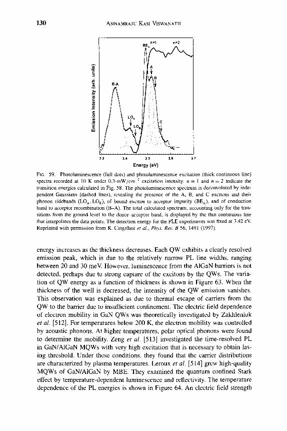
130 ANNAMRAJU KASI VISWANATH
E 3
m c o £ C o V)
to
E IXJ
B-A
BE." : ;
f ? A
f\/\B
y
•-o. / H i
n=2
* ;— . i.^ ^1.^.
Energy (eV)
FIG. 59. Photoluminescence (full dots) and photoluminescence excitation (thick continuous line) spectra recorded at 10 K under 0.3-mW/cm~^ excitation intensity, n = 1 and n = 2 indicate the transition energies calculated in Fig. 58. The photoluminescence spectrum is deconvoluted by inde-pendent Gaussians (dashed lines), revealing the presence of the A, B, and C excitons and their phonon sidebands ( L 0 A , L 0 B ) , of bound exciton to acceptor impurity (BE^), and of conduction band to acceptor recombination (B-A). The total calculated spectrum, accounting only for the tran-sitions from the ground level to the donor-acceptor band, is displayed by the thin continuous line that interpolates the data points. The detection energy for the PLE experiments was fixed at 3.42 eV. Reprinted with permission from R. Cingolani et ai, Phys. Rev. B 56, 1491 (1997).
energy increases as the thickness decreases. Each QW exhibits a clearly resolved emission peak, which is due to the relatively narrow PL line widths, ranging between 20 and 30 meV. However, luminescence from the AlGaN barriers is not detected, perhaps due to strong capture of the excitons by the QWs. The varia-tion of QW energy as a function of thickness is shown in Figure 63. When the thickness of the well is decreased, the intensity of the QW emission vanishes. This observation was explained as due to thermal escape of carriers from the QW to the barrier due to insufficient confinement. The electric field dependence of electron mobility in GaN QWs was theoretically investigated by Zakhleniuk et al. [512]. For temperatures below 200 K, the electron mobility was controlled by acoustic phonons. At higher temperatures, polar optical phonons were found to determine the mobility. Zeng et al. [513] investigated the time-resolved PL in GaN/AlGaN MQWs with very high excitation that is necessary to obtain las-ing threshold. Under these conditions, they found that the carrier distributions are characterized by plasma temperatures. Leroux et al [514] grew high-quality MQWs of GaN/AlGaN by MBE. They examined the quantum confined Stark effect by temperature-dependent luminescence and reflectivity. The temperature dependence of the PL energies is shown in Figure 64. An electric field strength

3 GROWTH AND OPTICAL PROPERTIES OF GAN 131
10°
/
7
' ' " " " 1
A /
1 •]
^ 1 ! / BE A LO, O B-A a n = 1 o n = 2 • !
3.6 3.7
Energy (eV)
FIG. 60. Intensity dependence of the luminescence spectra recorded at 4 K. The excitation power increases from bottom to top: 2.5 W/cm~^ 7.5 W/cm~^ 30 W/cm~^ 40 W/cm~^ and 70 W/cm"^ Inset: Intensity dependence of the integrated emission of the different luminescence bands. « = 1, the phonon replica, and /i = 2 are linear over 3 orders of magnitude, whereas BE^ and B-A exhibit a clear saturation above 20 W/cm~^. Reprinted with permission from R. Cingolani et ai, Phys. Rev. B 56, 1491 (1997).
of 450 KV/cm was determined. They concluded that the origin of the electric field is predominantly spontaneous polarization effects rather than piezoelectric effects in the well.
Suziki et al. [515] calculated electron scattering rates in GaN/AlGaN quan-tum wells. The intersubband scattering time was found to be dominated by LO-phonon scattering and was estimated as 100 fs. Im et al. [516] stud-ied the piezoelectric fields in GaN/ AlGaN quantum wells by time-resolved PL. A reduction in oscillator strength was observed that was attributed to piezoelectric fields. An increase in luminescence decay time with increasing well width was observed along with a red shift of the emission peaks. Recombination dynamics of free and localized excitons in MQWs of GaN/AlGaN was reported by Lefebvre et al. [517]. The decay times of excitons in both the wells and the barriers was found to be -^330 ps at 8 K. Spectral distribution of lifetimes was attributed to localization of carriers by potential fluctuations that arise due to alloy disorder and well width and depth variations. The radiative lifetime of free excitons in the low-temperature limit was estimated as 2.4 ps, which is much smaller than that for GaAs/GaAlAs MQWs. Suziki and lizuka [518] reported on the effect of the built-in field caused by the piezoelectric effect and the spontaneous polarization inherent in nitride quantum wells on the intersubband transition. Grandjean et al. [519] measured the PL of GaN quantum wells for

132 ANNAMRAJU KASI VISWANATH
c o
*S)
E lij
3.51 h
• > 3.50 h 10 K . \ 3L ^
• ,V:t5 3-»H
0 50 100 150 200 250 300
Temperature (K)
-^^ .
3.6 3.7 3.8
Energy (eV)
FIG. 61. Temperature dependence of the luminescence spectra recorded under power density of 50 W/cm~^. The n = 1 band persists up to room temperature. Inset: Thermal shift of the n = 1 band. The continuous curve is the best fit to the Varshni law. The dashed and dotted curves are the thermal shifts obtained for bulk GaN by different authors. Reprinted with permission from R. Cingolani et al, Phys. Rev. B 56, 1491 (1997).
D
(0
5) c 0) c
I c 8 0) c E 3 O x: CL
(a)
(b)
9MLs /
13 MLs /
GaN A /
15MLJ ; f^ 11 MLs
\ T = 9K
\ 5M Ls
7 MLs
J \ I 3 MLs
,...v (20
3.40 3.45 3.50 3.55 3 60 3.65 3.70
Photon energy (eV)
FIG. 62. 9-K photoluminescence spectra of GaN/Alg nGaoggN QWs that correspond to (a) sam-ple A and (b) sample B. Note the GaN buffer layer emission at 3.478 eV. Reprinted with permission from N. Grandjean and J. Massies, Appl Phys. Lett. 73, 1260 (1998).
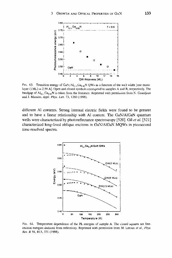
3 GROWTH AND OPTICAL PROPERTIES OF GAN 133
^ 3 . 7 5
^ 3 7 0
0)
S 3.60
c E 3.55
Al Ga N o i l 0 09
GaN
0 2 4 6 8 10 12 14 16
QW thickness (ML)
FIG. 63. Transition energy of GaN/Alo nGooggN QWs as a function of the well width [one mono-layer (IML) = 2.59 A]. Open and closed symbols correspond to samples A and B, respectively. The bandgap of AIQ uGaoggN is taken from the literature. Reprinted with permission from N. Grandjean and J. Massies, AppL Phys. Lett. 73, 1260 (1998).
different Al contents. Strong internal electric fields were found to be present and to have a linear relationship with Al content. The GaN/AlGaN quantum wells were characterized by photoreflectance spectroscopy [520]. Gil et al. [521] characterized long-lived oblique excitons in GaN/AlGaN MQWs in picosecond time-resolved spectra.
> 0)
Al,,Ga,,N/GaN QWs
QW(5 MLs)
0 SO 100 150 200 250 300
Temperature (K)
FIG. 64. Temperature dependence of the PL energies of sample A. The closed squares are free-exciton energies deduced from reflectivity. Reprinted with permission from M. Leroux et al, Phys. Rev. B 58, R13, 371 (1998).
134 ANNAMRAJU KASI VISWANATH
References
1. S. Strite, M. E. Lin, and H. Morkoc, Thin Solid Films 231, 197 (1993). 2. H. Morkoc, S. Strite, G. S. Gao, M. E. Lin, B. Sverdlov, and M. Bums, J. Appl. Phys. 73,
1363 (1994). 3. S. N. Mohammad, A. A. Salvador, and H. Morkoc, Proc. IEEE 83, 1306 (1995). 4. H. Morkoc, in "Semiconductor Heteroepitaxy" (B. Gil and R. L. Aulombard, Eds.),
pp. 238-249. World Scientific, Singapore, 1995. 5. T. D. Moustakas, J. L Pankove, and Y. Hamakawa, Eds., "Wide Bandgap Semiconductors,"
Vol. 242. Materials Research Society, Pittsburgh, PA, 1992. 6. M. Razeghi and A. Rogalski, J. Appl. Phys. 79, 7433 (1996). 7. S. Nakamura and G. Fasol, "The Blue Laser Diode." Springer-Veriag, Beriin, 1997. 8. R. F. Davis, Proc. IEEE 79, 702 (1991). 9. S. Nakamura, Solid State Commun. 102, 237 (1997).
10. B. Gil, Ed., "Group III Nitride Semiconductor Compounds." Clarendon, Oxford, 1998. 11. M. A. Khan, J. N. Kuznia, A. R. Bhattarai, and D. T. Olson, Appl. Phys. Lett. 62, 1786 (1993);
M. A. Khan, A. Bhattarai, J. N. Kuznia, and D. T. Olson, Appl. Phys. Lett. 63, 1214 (1993). 12. A. Gustafsson, M. E. Pistol, L. Montelius, and L. Samuelson, J. Appl. Phys. 84, 1715 (1998). 13. G. Popovici, H. Morkoc, and S. N. Mohammad, in "Group III Nitride Semiconductor Com-
pounds" (B. Gil, Ed.). Clarendon, Oxford, 1998. 14. R. Dingle, D. D. Sell, S. E. Stokowski, and M. Ilegems, Phys. Rev. B 4, 1211 (1971). 15. B. Monemar, Phys. Rev. B 10, 676 (1974). 16. J. L Pankove, J. E.Berkeyheiser,H.PMaruska, and J. Wittke,5o//J 5rflr CommM«. 8,1051 (1970). 17. S. Nakamura, M. Senoh, and T. Mukai, Jpn. J. Appl. Phys. 32, L8 (1998). 18. S. Nakamura, T. Mukai, and M. Senoh, Appl. Phys. Lett. 64, 1686 (1994). 19. S. Nakamura and T. Mukai, Jpn. J. Appl. Phys. 31, L1457 (1992). 20. S. Nakamura, T. Mukai, M. Senoh, and N. Isawa, Jpn. J. Appl. Phys. 31, L139 (1992). 21. S. Nakamura, M. Senoh, S. I. Nagahama, N. Isawa, T. Yamada, T. Matsushita, H. Kiyoku,
and Y. Sugimoto, Jpn. J. Appl. Phys. 35, L74 (1996). 22. S. Chichibu, T. Azuhata, T. Sota, and S. Nakamura, / Appl. Phys. 79, 2784 (1996). 23. Y. Kawakami, Z. G. Peng, Y. Narukawa, S. Fujita, S. Fujita, and S. Nakamura, Appl. Phys.
Lett. 69, 1414 (1996). 24. S. Chichibu, A. Shikanai, T. Azuhata, T. Sota, A. Kuramata, K. Horino, and S. Namamura,
Appl. Phys. Lett. 68, 3766 (1996). 25. A. Shikanai, T. Azuhata, T. Sota, S. Chichibu, A. Kuramata, K. Horino, and S. Nakamura,
J. Appl. Phys. 81, 417 (1997). 26. S. Nakamura, S. Masayuki, S. Nagahama, N. Iwasa, T. Yamada, T. Matsushita, Y. Sugimoto,
and K. Hiroyuki, Appl. Phys. Lett. 70, 1417 (1997). 27. A. Alemu, B. Gil, M. Julier, and S. Nakamura, Phys. Rev. B 57, 3761 (1998). 28. M. Julier, J. Campo, B. Gil, J. P Lascaray, and S. Nakamura Phys. Rev B 57, R6791 (1998). 29. S. Chichibu, H. Okumura, S. Nakamura, G. Feuillet, T. Azuhata, T. Sota, and S. Yoshida, Jpn.
J. Appl. Phys. 36, 1976 (1997). 30. S. Chichibu, T. Mizutani, T. Shoida, H. Nakanishi, T. Deguchi, T. Azuhata, T. Sota, and
S. Nakamura, Appl. Phys. Lett. 70, 3440 (1997). 31. S. Nakamura, Jpn. J. Appl. Phys. 30, 1620 (1991). 32. H. Amano, K. Hiramatsu, and I. Akasaki, Jpn. J. Appl. Phys. 27, L1384 (1988). 33. K. Naniwae, S. Itoh, H. Amano, K. Itoh, K. Hiramatsu, and I. Akasaki, J. Cryst. Growth 99,
381 (1990). 34. K. Hiramatsu, T. Detchprohm, and I. Akasaki, Jpn. J. Appl. Phys. 32, 1528 (1993). 35. H. Amano, M. Kito, K. Hiramatsu, and I. Akasaki, Jpn. J. Appl. Phys. 28, L2112 (1989). 36. D. Volm, K. Oettinger, T. Streibl, D. Kovalev, M. Ben-Chorin, J. Diener, B. K.
Meyer, J. Mejewski, L. Eckey, A. Hoffmann, H. Amano, I. Akasaki, K. Hiramatsu, and T. Detchprohm, Phys. Rev. B 53, 16,543 (1996).
3 GROWTH AND OPTICAL PROPERTIES OF GAN 135
37. C. Wetzel, D. Volm, B. K. Meyer, K. Pressel, S. Nilsson, E. N. Mokhov, and P. G. Baranov, Appl Phys. Lett. 65, 1033 (1994).
38. D. Kovalev, B. Averboukh, D. Volm, B. K. Meyer, H. Amano, and I. Akasaki, Phys. Rev. B 54, 2518 (1996).
39. B. K. Meyer, D. Volm, A. Graber, H. C. Alt, T. Detchprohm, A. Amano, and I. Akasaki, Solid State Commun. 95, 597 (1995).
40. T. Detchprohm, K. Hiramatsu, K. Itoh, and I. Akasaki, Jpn. J. Appl. Phys. 31, L1454 (1992). 41. D. Volm, T. Streibl, B. K. Meyer, T. Detchprohm, H. Amano, and I. Akasaki, Solid State
Commun. 96, 53 (1995). 42. M. Drechsler, D. M. Hofmann, B. K. Meyer, T. Detchprohm, H. Amano, and I. Akasaki, Jpn.
J. Appl Phys. 34, LI 178 (1995). 43. I. A. Buyanova, Mt. Wagner, W. M. Chen, B. Monemar, J. L. Lindstrom, H. Amano, and
I. Akasaki, Appl. Phys. Lett. 73, 2968 (1998). 44. S. Heame, E. Chason, J. Han, J. A. Floro, J. Figiel, J. Hunter, H. Amano, and I. S. T. Tsong,
Appl. Phys. Lett. 74, 356 (1999). 45. W. Shan, T. J. Schmidt, X. H. Yang. S. J. Hwang, J. J. Song, and B. Goldenberg, Appl Phys.
Lett. 66, 985 (1995). 46. W Shan, T. J. Schmidt, R. J. Haunstein, J. J. Song, and B. Goldenberg, Appl Phys. Lett. 66,
3492 (1995). 47. W. Shan, T. Schmidt, X. H. Yang, J. J. Song, and B. Goldenberg, J. Appl Phys. 79, 3691 (1996). 48. W Shan, R. J. Haunstein, A. J. Fischer, J. J. Song, W. G. Perry, M. D. Bremser, R. F. Davis,
and B. Goldenberg, Phys. Rev. B 54, 13,460 (1996). 49. W. Shan, B. D. Little, A. J. Fischer, J. J. Song, B. Goldenberg, W. G. Perry, M. D. Bremser,
and R. R Davis, Phys. Rev. B 54, 16,369 (1996). 50. A. J. Fischer, W. Shan, J. J. Song, Y C. Chang, R. Homing, and B. Goldenberg, Appl Phys.
Lett. 71, 1981 (1997). 51. W. Shan, A. J. Fischer, S. J. Hwang, B. D. Little, R. J. Haunstein, X. C. Xie, J. J. Song,
D. S. Kim, B. Goldenberg, R. Horing, S. Krishmamkutty, W. G Perry, M. D. Bremser, and R. F. Davis, /. Appl Phys. 83, 455 (1998).
52. M. Tchounkeu, O. Briot, B. Gil, J. P Alexis, and R. L. Aulombard, J. Appl Phys. 80, 5352 (1996).
53. B. Gil, O. Briot, and R. L. Aulombard, Phys. Rev B 52, R17,028 (1995). 54. B. Gil and A. Alemu, Phys. Rev B 56, 12,446 (1997). 55. B. Gil, S. Clur, and O. Briot, Solid State Commun. 104, 267 (1997). 56. G. D. Chen, M. Smith, J. Y Lin, H. X. Jiang, M. A. Khan, and C. J. Sun, Appl Phys. Lett.
67, 1653 (1995). 57. M. Smith, G D. Chen, J. Y Lin, H. X. Jiang, M. A. Khan, and C. J. Sun, Appl Phys. Lett.
67, 3295 (1995). 58. G D. Chen, M. Smith, J. Y Lin, H. X. Jiang, S. Wei, M. A. Khan, and C. J. Sun, Appl Phys.
Lett. 68, 2784 (1996). 59. M. Smith, G. D. Chen, J. Y Lin, H. X. Jiang, M. A. Khan, C. J. Sun, Q. Chen, and J. W. Yang,
J. Appl Phys. 79, 7001 (1996). 60. M. Smith, J. Y Lin, H. X. Jiang, and M. A. Khan, Appl Phys. Lett. 71, 635 (1997). 61. A. K. Viswanath, J. L Lee, S. Yu, D. Kim, Y Choi, and C. H. Hong, J. Appl Phys. 84, 3848
(1998). 62. A. K. Viswanath, J. L Lee, D. Kim, C. R. Lee, and J. Y Leem, Phys. Rev. B 58, 16,333 (1998). 63. A. K. Viswanath, J. L Lee, C. R. Lee, J. Y Leem, and D. Kim, Solid State Commun. 108,
483 (1998). 64. A. K. Viswanath, J. I. Lee, C. R. Lee, J. Y Leem, and D. Kim, Appl Phys. A 67, 551 (1998). 65. C. F. Li, Y S. Huang, L,. Malikova, and F. H. Pollak, Phys. Rev. B 55, 9251 (1997). 66. Y Li, Y Lu, H. Shem, M. Wraback, M. G. Brown, M. Schurman, L. Koszi, and R. A. Stall,
Appl Phys. Lett. 70, 2458 (1997).

136 ANNAMRAJU KASI VISWANATH
67. M. O. Manasreh, Phys. Rev. B 53, 16,425 (1996). 68. N. V. Edwards, S. D. Yoo, M. D. Bremser, T. W. Weeks, Jr., O. H. Nam, H. Liu, R. A. Stall,
M. N. Morton, N. R. Perkins, T. F. Kuech, and D. E. Aspnes, Appl Phys. Lett. 70, 2001 (1997). 69. S. Kim, I. R Herman, J. A. Tuchman, K. Doverspike, L. B. Rowland, and D. K. Gaskill, Appl.
Phys. Lett. 67, 380 (1995). 70. A. Saxler, D. Walker, R Kung, X. Zhang, M. Razheghi, J. Solomon, W. C. Mitchel, and
H. R. Vydyanath, Appl. Phys. Lett. 71, 3272 (1997). 71. D. A. Tumbull, X. Li, S. Q. Gu, E. E. Renter, J. J. Coleman, and S. G. Bishop, J. Appl. Phys.
80, 4609 (1996). 72. C. Y. Yeh, S. H. Wei, and A. Zunger, Phys. Rev. B 50, 2715 (1995). 73. K. Cho, Phys. Rev. B 14, 4463 (1976). 74. G. E. Pikus and L. G. Bir, "Symmetry and Strain-Induced Effects in Semiconductors." Wiley,
New York, 1974. 75. D. W. Langer, R. N. Euwema, K. Era, and T. Koda, Phys. Rev B 2, 4005 (1970). 76. M. Grynberg, Phys. Status. Solidi 27, 255 (1968). 77. J. E. Rowe, M. Cardona, and F. H. Pollak, in "Proceedings of the 1967 International Confer-
ence on II-VI Compounds" (D. G. Thomas Ed.). Benjamin, New York, 1967. 78. J. E. Rowe, M. Cardona, and F. H. Pollak, Solid State Commun. 6, 239 (1968). 79. A. A. Yamaguchi, Y. Mochizuki, C. Sasaoka, A. Kimura, M. Nido, and A. Usui, Appl. Phys.
Lett. 71, 374 (1997). 80. J. R. Haynes, Phys. Rev. Lett. 4, 351 (1960). 81. H. Frohlich, Adv. Phys. 3, 325 (1954). 82. J. Conradi and R. R Haering, Phys. Rev. Lett. 20, 1344 (1968). 83. E. Gross, S. Permogorov, V. Travinokov, and A. Selkin, J. Phys. Chem. Solids 31, 2595 (1970). 84. S. Permogorov, in "Modem Problems in Condensed Matter Sciences" (E. I. Rashba and
M. D. Sturge, Eds.), Vol. 2. North Holland, Amsterdam, 1982. 85. Y. S Park and J. R. Schneider, Phys. Rev Lett. 21, 798 (1968). 86. A. A Klochikhin, S. A. Permogorov, and A. N. Reznitsky, Sov Phys. JETP 44, 1176 (1976). 87. G. Popovici, H. Morkoc and S. N. Mohammad, in "Group III Nitride Semiconductor Com-
pounds" (B. Gil, Ed.). Clarendon, Oxford, 1998. 88. H. Morkoc, IEEE J. Select. Topics Quantum Electron. 4, 537 (1998). 89. S. Strite, B. Sariel, D. J. Smith, H. Chen, and H. Morkoc, J. Cryst. Growth 127, 204 (1993). 90. A. Botchkarev, A. Salvador, B. Sverdlov, J. Myoung, and H. Morkoc, J. Appl. Phys. 11, 4455
(1995). 91. M. Smith, G. D. Chen, J. Y. Lin, and H. X. Jiang, A. Salvador, B. N. Sverdlov, A. Botchkarev,
and H. Morkoc, Appl. Phys. Lett. 66, 3474 (1995). 92. D. J. Smith, D. Chandrasekhar, B. Sverdlov, A. Botchkarev, A. Salvador, and H. Morkoc,
Appl. Phys. Lett. 67, 1830 (1995). 93. M. Smith, G. D. Chen, J. Z. Li, J. Y Lin, H. X. Jiang, A. Salvador, W. K. Kim, O. Aktas,
A. Botchkarev, and H. Morkoc, Appl. Phys. Lett. 67, 3387 (1995). 94. Q. Zhu, A. Botchkarev, W. Kim, O. Aktas, A. Salvador, B. Sverdlov, H. Morkoc, S. C. Y. Tsen,
and D. J. Smith, Appl. Phys. Lett. 68, 1141 (1996). 95. D. C. Reynolds, D. C. Look, W. Kim, O. Aktas, A. Botchkarev, A. Salvador, H. Morkoc, and
D. N. Talwar, J. Appl. Phys. 80, 594 (1996). 96. G. D. Chen, M. Smith, J. Y Lin, H. X. Jiang, A. Salvador, B. N. Sverdlov, A. Botchkarev,
and H. Morkoc, / Appl. Phys. 79, 2675 (1996). 97. W. Kim, O. Aktas, A. E. Botchkarev, A. Salvador, S. N. Mohammad, and H. Morkoc, J. Appl.
Phys. 79, 7657 (1996). 98. Z. X. Liu, S. Pau, K. Syassen, J. Kuhl, W. Kim, H. Morkoc, M. A. Khan, and C. J. Sun, Phys.
Rev. B 58, 6696 (1998). 99. J. Petalas, S. Logothetidis, S. Boultadakis, M. Alouani, and J. M. Wills, Phys. Rev B 52, 8082
(1995).

3 GROWTH AND OPTICAL PROPERTIES OF GAN 137
100. H. Teisseyre, P. Pertin, T. Suski, I. Grzegory, S. Porowski, J. Jun, A. Pietraszko, and T. D. Moustakas, J. Appl. Phys. 76, 2429 (1994).
101. C. Trager-Cowan, K. P O. Donnell, S. E. Hooper, and C. T. Foxon, Appl Phys. Lett. 68, 355 (1996).
102. Z. Yu, S. L. Buczkowski, N. C. Giles, T. H. Myers, and M. R. Richards-Babb Appl Phys. Lett. 69, 2731 (1996).
103. Y. Zhao, C. W. Tu, I. T. Bae, and T. Y Seong, Appl Phys. Lett. 74, 3182 (1999). 104. S. H. Cho, T. Maruyama, and K. Akimoto, Jpn. J. Appl Phys. 34, L1575 (1995). 105. K. Iwata, H. Asahi, S. J. Yu, K. Asami, H. Fujita, M. Fushida, and S. Gonda, Jpn. J. Appl
Phys. 35, L289 (1996). 106. K. Komitzer, K. Thonke, R. Sauer, M. Mayer, M. Kamp, and K. J. Ebeling, J. Appl Phys.
83, 4397 (1998). 107. C. Heinlein, J. K. Grepstad, S. Einfeldt, D. Hommel, T. Berge, and A. P Grande, J. Appl
Phys. 83, 6023 (1998). 108. Z. J. Yu. B. S. Sywe, A. U. Ahmed, and J. H. Edgar, J. Electron. Mater. 21, 383 (1992). 109. Y Okamoto, S. Hashiguchi, Y Okada, and M. Kawabe, Jpn. J. Appl Phys. 37, LI 109 (1998). 110. Y Shimizu, T. Tominari, S. Hokuto, Y Chiba, and Y Nanishi, Jpn. J. Appl Phys. 37, L700
(1998). 111. T. W. Kang, S. H. Park, H. D. Cho, M. Y Kwak, G. S. Eom, and T. W. Kim, Jpn. J. Appl
Phys. 37, 4417 (1998). 112. N. Grandjean, M. Leroux, M. Langt, and J. Massies, Appl Phys. Lett. 71, 240 (1997). 113. M. E. Lin, B. N. Sverdlov, and H. Morkoc, J. Appl Phys. 74, 5038 (1993). 114. N. Grandjean, J. Massies, P. Vennegues, M. Leroux, F. Demangeot, M. Renucci, and
J. Frandon, J. Appl Phys. 83, 1379 (1998). 115. N. Grandjean, J. Massies, F. Semond, S. Y Karpov and R. A. Talalaev, Appl Phys. Lett. 74,
1854 (1999). 116. A. Krtschil, H. Witte, M. Lisker, J. Christen, U. Birkle, S. Einfeldt, and D. Hommel, Appl
Phys. Lett. 74, 2032 (1999). 117. H. Tang and J. B. Webb, Appl Phys. Lett. 14, 2373 (1999). 118. X. Q. Shen, P Ramvall, P Riblet, and Y Aoyagi, Jpn. J Appl Phys. 38, L411 (1999). 119. Y Okamoto, S. Hashiguchi, Y Okada, and M. Kawabe, Jpn. J Appl Phys. 38, L230 (1999). 120. S. Strite, J. Ruan. Z. Li, N. Manning, A. Salvador, H. Chen, D. J. Smith, W. J. Choyke, and
H. Morkoc, J Vac. ScL Technol, B 9, 1924 (1991). 121. E. Kim, L Berishev, A. Bensaoula, L Rusakova, K. Waters, and J. A. Schultz, J. Appl Phys.
85, 1178(1999). 122. N. Grandjean, M. Leroux, J. Massies, M. Mesrine, and M. Laugt, Jpn. J. Appl Phys. 38, 618
(1999). 123. W. Widmann, G. Feuillet, B. Daudin, and J. L. Rouviere, J. Appl Phys. 85, 1550 (1999). 124. M, E. Lin, B. Sverdlov, G L. Zhou, and H. Morkoc, Appl Phys. Lett. 62, 3479 (1993). 125. S. Yoshida, S. Misawa, and S. Gonda, Appl Phys. Lett. 42, 427 (1983). 126. Z. Yang, L. K. Li, and W. L Wang, Appl Phys. Lett. 67, 1686 (1995). 127. W. S. Wong, N. Y Li, H. K. Dong, F Deng, S. S. Lau, C. W. Tu, J. Hays, S. Bidnyk, and
J. J. Song, J. Cry St. Growth 164, 159 (1996). 128. N. Grandjean and J. Massies, Appl Phys. Lett. 71, 240, 1816 (1997). 129. W. Shan, A. J. Fischer, J. J. Song, G E. Bulman, H. S. Kong, M. T. Leonard, W. G Perry,
M. D. Bremser, and, R. E Davis, Appl Phys. Lett. 69, 740 (1996). 130. L A. Buyanova, J. P. Bergman, B. Monemar, H. Amano, and, L Akasaki, Appl Phys. Lett.
69, 1255 (1996). 131. T. Sasaki and T. Matsuoka, J Appl Phys. 64, 4531 (1988). 132. S. Chichibu, T. Azuhata, T. Sota, H. Amano, and I. Akasaki, Appl Phys. Lett. 70, 2085 (1997). 133. T. W. Weeks, M. D. Bremser, K. S. Ailey, E. Carlson, W. G Perry, and R. F. Davis, Appl
Phys. Lett. 67, 401 (1995).

138 ANNAMRAJU KASI VISWANATH
134. F. R. Chien, X. J. Ning, S. Stemmer, P. Pirouz, M. D. Bremsev, and R. R Davis, Appl. Phys. Lett. 68, 2678 (1996).
135. T. Nishida, T. Akasaka, and N. Kobayashi, Jpn. J. Appl. Phys. 31, L459 (1998). 136. X. Q. Shen, S. Tanaka, S. Iwai, and Y. Aoyagi, Jpn. J. Appl. Phys. 37, L637 (1998). 137. V. M. Torres, M. Stevens, J. L. Edwards, D. J. Smith, R. B. Doak, and I. S. T. Tsong, Appl.
Phys. Lett. 71, 1365 (1997). 138. F. Boscherini, R. Lantier, A. Rizzi, F. D'Acapito, and S. Mobilio, Appl. Phys. Lett. 74, 3308
(1999). 139. M. A. L. Johnson, J. D. Brown, N. A. El Masry, J. W. Cook, Jr., J. F Schetzina, H. S. Kong,
and J. A. Edmond, J. Vac. Sci. Technol, B 16, 1282 (1998). 140. H. Okumura, H. Hamaguchi, G. Feuillet, Y. Ishida, and S. Yoshida, Appl. Phys. Lett. 72, 3056
(1998). 141. F Hamdani, A. Botchkarev, W. Kim, H. Morkoc, M. Yeadon, J. M. Gibson, S. C. Y Tsen, D. J.
Smith, D. C. Reynolds, D. C. Look, K. Evans, C. W. Litton, W. C. Mitchel, and R Hemenger, Appl. Phys. Lett. 70, 467 (1997).
142. F Hamdani, A. E. Botchkarev, H. Tang, W. Kim, and H. Morkoc, Appl. Phys. Lett. 71, 3111 (1997).
143. G. Popovici, W. Kim, A. Botchkarev, H. Tang, H. Morkoc, and J. Soloman, Appl. Phys. Lett. 71, 3385 (1997).
144. F. Hamdani, M. Yeadon, D. J. Smith, H. Tang, W. Kim, A. Salvador, A. E. Botchkarev, J. M. Gibson, A. Y. Polyakov, M. Skowronski, and H. Morkoc, / Appl. Phys. 83, 983 (1998).
145. X. W. Sun, R. F. Xiao, and H. S. Kwok, J. Appl. Phys. 84, 5776 (1998). 146. R Kung, A. Saxler, X. Zhang, D. Walker, R. Lavado, and M. Rezeghi, Appl. Phys. Lett. 69,
2116(1996). 147. T. Ishi, M. Mukaida, T Nishihara, S. Hayashi, and M. Shinohara, Jpn. J. Appl. Phys. 37, L672
(1998). 148. A. Kuramata, K. Horino, K. Domen, and K. Shinohera, Appl. Phys. Lett. 67, 2521 (1995). 149. T George, E. Jacobson, W. Pike, P. Chang-chein, M. Khan, J. Yang, and S. Mahajan, Appl.
Phys. Lett. 68, 337 (1996). 150. C. Sun, J. Yang, Q. Chen, M. Khan, T. George, P Chang-chien, and S. Mahajan, Appl. Phys.
Lett. 68, 1129(1996). 151. S. A. Nikishin, H. Terkin, V. G. Antipov, A. I. Guriev, A. S. Zubrilov, V. A. Elyukhin,
N. N. Faleev, R. N. Kyutt, and A. K. Chin, Appl. Phys. Lett. 72, 2361 (1998). 152. G. Ramirez-Flores, H. Navarro-Contreras, A. Lastras-Martinez, R. C. Powell, and J. E. Greene,
Phys. Rev. B 50, 8433 (1994). 153. R. C. Powell, N. E. Lee, Y. W. Kim, and J. E. Greene, J. Appl. Phys. 73, 189 (1993). 154. M. A. Vidal, G. Ramirez-Flores, H. Navarro-Contreras, A. Lastras-Martinez, R. C. Powell,
and J. E. Greene, Appl. Phys. Lett. 68, 441 (1996). 155. P. Perlin, Y. Gorczyca, N. E. Christensen, Y Grzegory, H. Teiserye, and T. Suski, Phys. Rev.
B 45, 13,307 (1992). 156. A. Strittmatter, A. Krost, M. Strabburg, V. Turck, D. Bimberg, J. Biasing, and J. Christen,
Appl. Phys. Lett. 74, 1242 (1999). 157. X. Zhang, S. J. Chua, R Li, K. B. Chong, and Z. C. Feng, Appl. Phys. Lett. 74, 1984 (1999). 158. H. Ishikawa, G. Y Zhao, N. Nakada, T. Egawa, T Jimbo, and M. Umeno, Jpn. J. Appl. Phys.
38, L492 (1999). 159. N. R Kobayashi, J. T. Kobayashi, R D. Dapkus, W. J. Choi, A. E. Bond, X. Zhang, and
D. H. Rich, Appl. Phys. Lett. 71, 3569 (1997). 160. A. J. Steckl, J. Devrajan, C. Tran, and R. A. Stall, Appl. Phys. Lett. 69, 2264 (1996). 161. J. Cao, D. Pavlidis, A. Eisenbach, A. Philippe, C. Bru-Chevallier, and G. Guillot, Appl. Phys.
Lett. 71, 3880 (1997). 162. J. Cao, D. Pavlidis, Y Park, J Singh, and A. Eisenbach, J. Appl. Phys. 83, 3829 (1998).

3 GROWTH AND OPTICAL PROPERTIES OF GAN 139
163. S. I. Molina, A. M. Sanchez, F. J. Pacheco, R. Garcia, M. A. Sanchez-Garcia, F. J. Sanchez, and E. Callja, AppL Phys. Lett. 74, 3362 (1999).
164. Y. Nakada, I. Aksenov, and H. Okumura, Appl. Phys. Lett. 73, 827 (1998). 165. I. Berishev, A. Bensaoula, I. Rusakova, A. Karabutov, M. Ugarov, and V. P. Ageev, Appl.
Phys. Lett. 73, 1808 (1998). 166. N. P Kobayashi, J. T. Kobayashi, W. J. Choi, and P D. Dapkus, Appl. Phys. Lett. 73,1553 (1998). 167. Y. Hiroyama and M. Tamura, Jpn. J. Appl. Phys. 31, L630 (1998). 168. T. Lei, M. Fanciulli, R. J. Molnar, T. D. Moustakas, R. J. Graham, and J. Scanlon, Appl. Phys.
Lett. 59, 944 (1991). 169. E. Calleja, M. A. Sanchez-Garcia, D. Basak, F J. Sanchez, F. Calle, P. Youinou, E. Munoz,
J. J. Serrano, J. M. Blanco, C. Villar, T. Laine, J. Gila, K. Sarrinen, P Hautojarvi, C. H. Molloy, D. J. Somerford, and I. Harrison, Phys. Rev. B 58, 1550 (1998).
170. C. H. Hong, D. Pavilidis, S. W. Brown, and S. C. Rand, / Appl. Phys. 11, 1705 (1995). 171. A. A. Yamaguchi, T. Manako, A. Akai, H. Sunakawa, A. Kimura, M. Nido, and A. Usui, Jpn.
J. Appl. Phys. 35, L873 (1996). 172. X. L. Sun, H. Yang, L. X. Zheng, D. P Xu, J. B. Li, Y. T. Yang, G. H. Li, and Z. G. Wang,
Appl. Phys. Lett. 74, 2827 (1999). 173. J. Wu, H. Yaguchi, K. Onabe, R. Ito, and Y Shiraki, Appl. Phys. Lett. 71, 2067 (1997). 174. J. Wu, H. Yaguchi, K. Onabe, Y Shiraki, and R. Ito, Jpn. J Appl. Phys. 37, 1440 (1998). 175. H. Tsuchiya, K. Sunaba, M. Minami, T. Suemasu, and F Hasegawa, Jpn. J. AppL Phys. 37,
L568 (1998). 176. M. Sato, J Appl. Phys. 78, 2123 (1995). 177. S. Strite, J. Ruan, Z. Li, A. Salvador, H. Chen, D. J. Smith, W. J. Choyke, and H. Morkoc,
/ Vac. Sci. Technol. 89, 1924 (1991). 178. X. W. Lin, M. Behar, R. Maltez, W. Swider, Z. Liliental-Weber, and J. Washburn, Appl. Phys.
Lett. 67, 2699 (1995). 179. D. E. Lacklison, J. W. Orton, I. Harrison, T. S. Cheng, L. C. Jenkins, C. T. Foxon, and
S. E. Hooper, / Appl. Phys. 78, 1838 (1995). 180. J. Menniger, U. Jahn, O. Brandt, H. Yang, and K. Ploog, Phys. Rev. B 53, 1881 (1996). 181. H. Yang, O. Brandt, M. Wassermeier, J. Behrend, H. P Schonherr, and K. H. Ploog, Appl.
Phys. Lett. 68, 244 (1996). 182. S. A. Nikishin, V. G. Antipov, S. S. Ruvimov, G A. Seryogin, and H. Temkin, Appl. Phys.
Lett. 69, 3227 (1996). 183. O. Brandt, H. Yang, A. Trampert, M. Wassermeier, and K. H. Ploog, Appl. Phys. Lett. 71,
473 (1997). 184. D. J. As, R Schmilgus, C. Wang, B. Schottker, D. Schikora, and K. Lischka, Appl. Phys. Lett.
70, 1311 (1997). 185. G. Lupke, O. Busch, C. Meyer, H. Kurz, O. Brandt, H. Yang, A. Trampert, K. H. Ploog, and
G. Lucovsky, Phys. Rev. B 57, 3722 (1998). 186. G. Mirjalili, T. J. Parker, S. F Shayesteh, M. M. Bulbul, S. R. P Smith, T. S. Cheng, and
C. T. Foxon, Phys. Rev. B 57, 4656 (1998). 187. S. Shokhovets, R. Goldhahn, V. Cimalla, T. S. Cheng, and C. T. Foxon, J. Appl. Phys. 84,
1561 (1998). 188. U. Kohler, D. J. As, B. Schottker, T. Frey, K. Lischka, J. Scheiner, S. Shokhovets, and
R. Goldhahn, / Appl. Phys. 85, 404 (1999). 189. J. H. Li, H. Chen, L. C. Cai, S. F Cui, W. X. Yu, J. M. Zhou, Q. Huang, Z. H. Mai,
W. L. Zheng, and Q. J. Jia, Appl. Phys. Lett. 74, 2981 (1999). 190. K. Das and D. K. Ferry, Solid State Electron. 19, 851 (1976). 191. H. Yang, O. Brandt, and K. Ploog, Phys. Status Solidi B 194, 109 (1996). 192. A. Gassmann, T. Suski, N. Newman, C. Kisielowski, E. Jones, E. R. Weber,
Z. Liliental-Weber, M. D. Rubin, H. I. Helava, I. Grzegory, M. Bockowski, J. Jun, and S. Porowski, J Appl. Phys. 80, 2195 (1996).
140 ANNAMRAJU KASI VISWANATH
193. K. P. Korona, A. Wysmolek, K. Pakula, R. Stepniewski, J. M. Baranowski, I. Grzegory, B. Lucznik, M. Wroblewski, and S. Porowski, Appl. Phys. Lett. 69, 788 (1996).
194. K. Pakula, A. Wysmolek, K. P. Korona, J. M. Baranowski, R. Stepniewski, I. Grzegory, M. Bockowski, J. Jun, S. Krukowski, M. Wroblewski, and S. Porowski, Solid State Commun. 97, 919 (1996).
195. S. Kurai, T. Abe, Y. Naoi, and S. Sakai, Jpn. J. Appl. Phys. 35, 1637 (1996). 196. K. Naniwae, S. Itoh, H. Amano, K. Itoh, K. Hiramatsu, and I. Akasaki, / Cryst. Growth 99,
381 (1990). 197. B. D. Joyce and J. A. Bradley, Nature 195, 458 (1962). 198. A. Sakai, Appl. Phys. Lett. 71, 2259 (1997). 199. D. Kapolnek, S. Keller, R. Vetury, R. D. Underwood, P Kozodoy, S. R Den Baars, and
U. K. Mishra, Appl. Phys. Lett. 71, 1204 (1997). 200. D. Kapolnek, X. H. Wu, B. Keying, S. Keller, B. P Keller, U. K. Mishra, S. P Den Baars,
and J. S. Speck, Appl. Phys. Lett. 67, 1541 (1995). 201. T. S. Zheleva, O. H. Nam, M. D. Bremser, and R. F. Davis, Appl. Phys. Lett. 71, 2472 (1997). 202. O. H. Nam, M. D. Bremser, T. S. Zheleva, and R. F. Davis, Appl. Phys. Lett. 71, 2638 (1997). 203. A. Usui, H. Sunakawa, A. Sakai, and A. A. Yamaguchi, Jpn. J. Appl. Phys. 36, 899 (1997). 204. A. Sakai, H. Sunakawa, and A. Usui, Appl. Phys. Lett. 71, 2259 (1997). 205. Y Kawaguchi, Y Honda, H. Matsushima, M. Yamaguchi, K. Hiramatsu, and N. Sawaki, Jpn.
J Appl. Phys. 37, L966 (1998). 206. J. A. Freitas, Jr., O. H. Nam, R. F. Davis, G. V. Saparin, and S. K. Obyden, Appl. Phys. Lett.
72, 2990 (1998). 207. Y Kawaguchi, S. Nambu, H. Sone, T. Shibata, H. Matsushima, M. Yamaguchi, H. Miyake,
K. Hiramatsu, and N. Sawaki, Jpn. J Appl. Phys. 37, L845 (1998). 208. J. Wang, S. Tattori, H. Sato, M. S. Hao, Y Ishikawa, T. Sugahara, K. Yamashita, and S. Sakai,
Jpn. J Appl. Phys. 37, 4475 (1998). 209. J. Park, P A. Grudowski, C. J. Eiting, and R. D. Dupuis, Appl. Phys. Lett. 73, 333 (1998). 210. X. Li, G. Bishop, and J. J. Coleman, Appl. Phys. Lett. 73, 1179 (1998). 211. F. Bertram, T. Riemann, J. Christen, A. Kaschner, A. Hoffmann, C. Thomsen, K. Hiramatsu,
T. Shibata, and N. Sawaki, Appl. Phys. Lett. 74, 359 (1999). 212. P Kung, D. Walker, M. Hamilton, J. Diaz, and M. Razeghi, Appl. Phys. Lett. 74, 570 (1999). 213. K. C. Zeng, J. Y Lin, H. X. Jiang, and W. Yang, Appl. Phys. Lett. 74, 1227 (1999). 214. S. J. Rosner, G. Girolami, H. Marchand, P T. Fini, J. P Ibbeston, L. Zhao, S. Keller,
U. K. Mishra, S. P Den Baars, and J. S. Speck, Appl. Phys. Lett. 74, 2035 (1999). 215. T. S. Zheleva, W. M. Ashmawi, O. H. Nam, and R. F. Davis, Appl. Phys. Lett. 74, 2492 (1999). 216. M. Hao, S. Mahanty, T. Sugahara, Y Morishina, H. Takenaka, J. Wang, S. Tottori, K. Nishino,
Y Naoi, and S. Sakai, J Appl. Phys. 85, 6497 (1999). 217. N. P Kobayashi, J. T. Kobayashi, X. Zhang, P D. Dapkus, and D. H. Rich, Appl. Phys. Lett.
74, 2836 (1999). 218. Q. K. K. Liu, A. Hoffmann, H. Siegle, A. Kachner, C. Thomsen, J. Christen, and F. Bertram,
Appl. Phys. Lett. 74, 3122 (1999). 219. A. Kaschner, A. Hoffmann, C. Thomsen, F. Bertram, T Riemann, J. Christen, K. Hiramatsu,
T. Shibata, and N. Sawaki, Appl. Phys. Lett. 74, 3320 (1999). 220. A. J. Fischer, W. Shan, G. H. Park, J. J. Song, D. S. Kim, D. S. Ye, R. Homing, and
B. Goldenberg, Phys. Rev. B 56, 1077 (1997). 221. S. Pau, J. Kuhl, F. Scholz, V. Haerle, M. A. Khan, and C. J. Sun, Appl. Phys. Lett. 72, 557
(1998). 222. S. Pau, J. Kuhl, F. Scholz, V. Haerle, M. A. Khan, and C. J. Sun, Phys. Rev. B 56, R12,718
(1997). 223. R. Zimmermann, A. Euteneuer, J. Mobius, D. Weber, M. R. Hofmann, W. W Ruble,
E. O. Gobel, B. K. Meyer, H. Amano, and I. Akasaki, Phys. Rev B 56, R12,722 (1997).

3 GROWTH AND OPTICAL PROPERTIES OF GAN 141
224. T. J. Schmidt, J. J. Song, J. C. Chang, R. Homing, and B. Goldenberg, Appl. Phys. Lett. 72, 1504 (1998).
225. H. Haag, P. Gilliot, R. Levy, B. Honerlage, O. Briot, S. Rufenach-Clur, and R. L. Aulombard, Appl Phys. Lett. 74, 1436 (1999).
226. H. Haag, P Gilliot, R. Levy, B. Honerlage, O. Briot, S. Rufenach-Clur, and R. L. Aulombard, Phys. Rev. B 59, 2254 (1999).
227. T. Aoki, G. Mohs, M. Kuwata-Gonokami, and A. A. Yamaguchi, Phys. Rev. Lett. 82, 3108 (1999).
228. H. Ye, G. W. Wicks, and P M. Fauchet, Appl. Phys. Lett. 74, 711 (1999). 229. D. N. Hahn, G. T. Kiehne, J. B. Ketterson, G. K. L. Wong, P Kung, A. Saxler, and M. Razeghi,
J. Appl. Phys. 85, 2497 (1999). 230. Y Narukawa, Y. Kawakami, M. Funato, S. Fujita, S. Fujita, and S. Nakamura, Appl. Phys.
Lett. 70, 981 (1997). 231. Y Toyozawa, Prog. Theor. Phys. 20, 53 (1958); / Phys. Chem. Solids 25, 59 (1964). 232. B. Segall and G. D. Mahan, Phys. Rev. 171, 935 (1968). 233. B. Segall, Phys. Rev 150, 734 (1966); 163, 769 (1967); G E. Hite, D. T. F Marple, M. Aven,
and B. Segall, Phys. Rev 156, 850 (1967). 234. B. segall, in "Proceedings of the IX Conference on the Physics of Semiconductors"
(S. M. Ryvkin, Ed.), p. 425. Nauka, Leningrad, 1968. 235. S. Rudin, T. L. Reinecke, and B. Segall, Phys. Rev B 42, 11,218 (1990). 236. M. Ilegems, R. Dingle, and R. A. Logan, J. Appl. Phys. 43, 3797 (1972). 237. T. Azuhata, T. Sota, K. Suziki, and S. Nakamura, J. Phys.: Condens. Matter 7, L129 (1995). 238. A. S. Barker, Jr. and M. Ilegems, Phys. Rev B 7, 743 (1973). 239. A. J. Fischer, D. S. Kim, J. Hays, W. Shan, J. J. Song, D. B. Eason, J. Ren, J. F. Schetzina,
H. Luo, J. K. Furdyna, Z. Q. Zhu, T. Yao, J. F Klem, and W. Schafer, Phys. Rev. Lett. 73, 2368 (1994).
240. R. Hellman, M. Koch, J. Feldman, S. T. Cundiff, E. O. Gobel, D. R. Yakovlev, A. Waag, and G. Landwehr, Phys. Rev B 48, 2847 (1999).
241. T. Li, A. J. Lozykowski, and J. L. Reno, Phys. Rev B 46, 6961 (1992). 242. M. O. Neil, M. Oestreich, W W. Ruble, and D. E. Ashenford, Phys. Rev B 48, 8980 (1993). 243. D. Lee, A. M. Johnson, J. E. Zucker, R. D. Feldman, and R. F. Austin, J. Appl. Phys. 69,
6722 (1991). 244. N. T. Pelekanos, J. Ding, M. Hagerott, A. V. Nurmikko, H. Luo, N. Samarth, and J. K. Fur-
dyna, Phys. Rev B 45, 6037 (1992). 245. D. S. Chemla, D. A. B. Miller, P W. Smith, A. C. Gossard, and W. Wiegmann, IEEE J. Quan-
tum Electron. 20, 265 (1984). 246. D. A. B. Miller, D. S. Chemla, D. J. Eilenberger, P W. Smith, A. C. Gossard, and W. T. Tsang,
Appl. Phys. Lett. 41, 679 (1982). 247. Y S. Huang, A. Qiang, R H. Pollak, G D. Pettit, P D. Kirchner, and L. B. Sorensen, /. Appl.
Phys. 70, 7537 (1991). 248. J. Lee, E. S. Koteles, and M. O. Vassell, Phys. Rev B 33, 5512 (1986). 249. A. Tookey, G Brown, B. Vogele, D. Bain, I. J. Blewett, A. K. Kar, I. Galbraith, K. A. Prior,
B. C. Cavenett, and B. S. Wherrett, "Proceedings of the International Quantum Electronics Conference," paper QWE 2. Optical Society of America, San Francisco, 1998.
250. P. Borri, W. Langbein, J. M. Hvam, and F. Martelli, "Proceedings of the International Quantum Electronics Conference," paper QWE 3. Optical Society of America, San Francisco, 1998.
251. W. Shan, X. C. Xie, J. J. Song, and B. Goldenberg, Appl. Phys. Lett. 67, 2512 (1995). 252. C. I. Harris, B. Monemar, H. Amano, and I. Akasaki, Appl. Phys. Lett. 67, 840 (1995). 253. Y Kawakami, Z. G Peng, Y Narukawa, S. Fujita, S. Fujita, and S. Nakamura, Appl. Phys.
Lett. 69, 1414 (1996). 254. J. S. Im, A. Moritz, F Steuber, V. Harle, F Scholz, and A. Hangleiter, Appl. Phys. Lett. 70,
631 (1997).

142 ANNAMRAJU KASI VISWANATH
255. S. Pau, J. Kuhl, M. A. Khan, and C. J. Sun, Phys. Rev. B 58, 12,916 (1998). 256. S. Pau, Z. X. Liu, J Kuhl, J. Ringling, H. T. Grahn, M. A. Khan, C. J. Sun, O. Ambacher,
and M. Stutzman, Phys. Rev. B 57, 7066 (1998). 257. M. Godlewski, J. P. Bergman, B. Monemar, U. Rossner, and A. Barski, Appl Phys. Lett. 69,
2089 (1996). 258. L. Eckey, J. Ch. Hoist, R Maxim, R. Heitz, A. Hoffman, I. Broser, B. K. Meyer, C. Wetzel,
E. N. Mokhov, and P G. Baranov, Appl. Phys. Lett. 68, 415 (1996). 259. O. Brandt, B. Yang, H. J. Wunsche, U. Jahn, J. Ringhng, G. Paris, H. T. Grahn, and
K. H. Ploog, Phys. Rev. B 58, R 13,407 (1998). 260. B. Monemar, J. P. Bergman, I. G. Ivanov, J. M. Baranowski, K. Pakula, I. Grzegory, and
S. Porowski, Solid State Commun. 104, 205 (1997). 261. R. Klann, O. Brandt, H. Yang, H. T. Grahn, and K. H. Ploog, Appl. Phys. Lett. 70, 1808
(1997). 262. R. Klann, O. Brandt, H. Yang, H. T. Grahn, K. Ploog, and A. Trampert, Phys. Rev. B 52,
Rl 1,615 (1995). 263. D. Yonder Linde, J. Kuhl, and E. Rosengart, J. Lumin. 24/25, 675 (1981). 264. D. Rosen, A. G. Doukas, Y. Budansky, A. Katz, and R. R. Alfano, Appl. Phys. Lett. 39, 935
(1981). 265. R. Strobel, R. Eccleston, J. Kuhl, and K. Kohler, Phys. Rev. B 43, 12,564 (1991). 266. V. Emiliani, S. Ceccherini, F. Bogani, M. Colocci, A. Frova, and S. S. Shi, Phys. Rev. B 56,
4807 (1997). 267. M. Jorgensen and J. M. Hvam, Appl. Phys. Lett. 43, 460 (1983). 268. M. B. Johnson, T. C. McGill, and A. T. Hunter, J. Appl. Phys. 63, 2077 (1988). 269. A. M. de Paula, J. F Ryan, H. J. W. Eakin, M. Tatham, R. A. Taylor, and A. J. Turberfield,
/ Lumin. 59, 303 (1994). 270. J. L. A. Chilla, O. Buccafusca, and J. J. Rocca, Phys. Rev. B 48, 14,347 (1993). 271. H. J. W. Eakin and J. F Ryan, J. Lumin. 40/41, 553 (1998). 272. A. von Lehmen and T. M. Ballantyne, Appl. Phys. Lett. 44, 87 (1983). 273. J. I. Pankove, E. A. Miller, and J. E. Berkeyheiser, RCA Rev. 32, 383 (1971). 274. J. I. Pankove, E. A. Miller, D. Richman, and J. E. Berkeyheiser, J. Lumin. 4, 63 (1971). 275. J. I. Pankove, E. A. Miller, and J. E. Berkeyheiser, J. Lumin. 5, 84 (1972). 276. J. I. Pankove, E. A. Miller, and J. E. Berkeyheiser, J. Lumin. 6, 54 (1973). 277. H. P Maruska, D. A. Stevenson, and J. I. Pankove, Appl. Phys. Lett. 22, 303 (1973). 278. H. P Maruska, W. C. Rhines, and D. A. Stevenson, Mater. Res. Bull. 7, 777 (1972). 279. A. Shintani and S. Minagawa, J. Electrochem. Soc. 123, 1725 (1976). 280. M. Ilegems, R. Dingle, and R. A. Logan, / Appl. Phys. 43, 3797 (1972). 281. M. Ilegems and R. Dingle, J. Appl. Phys. 44, 4234 (1973). 282. O. Lagerstedt and B. Monemar, J. Appl. Phys. 45, 2266 (1974). 283. B. Monemar, O. Lagerstedt, and H. P Gislason, / Appl. Phys. 51, 625 (1980). 284. B. Monemar, H. P Gislason, and O. Lagerstedt, / Appl. Phys. 51, 640 (1980). 285. P Bergman, G. Ying, B. Monemar, and P O. Holtz, J. Appl. Phys. 61, 4589 (1987). 286. J. L Pankove, J. E. Berkeyheiser, and E. A. Miller, / Appl. Phys. 45, 1280 (1974); J. I. Pankove
and J. E. Berkeyheiser, J. Appl. Phys. 45, 3892 (1974). 287. J. I. Pankove and J. A. Hutchby, J. Appl. Phys. 47, 5387 (1976). 288. M. Boulou, M. Furtado, G. Jacob, and D. Bois, J. Lumin. 18/19, 767 (1979). 289. G. Jacob, M. Boulou, and M. Furtado, J. Cryst. Growth 42, 136 (1977). 290. J. L Pankove, M. T. Duffy, E. A. Miller, and J. E. Berkeyheiser, J. Lumin. 8, 89 (1973). 291. T. Ogino and M. Aoki, Jpn. J. Appl. Phys. 19, 2395 (1980). 292. E. Ejder and H. G. Grimmeiss, J. Appl. Phys. 5, 275 (1974). 293. L Akasaki, H. Amano, M. Kito, and K. Hiramatsu, J. Lumin. 48/49, 666 (1991). 294. S. Nakamura, N. Iwasa, M. Senoh, and T. Mukai, Jpn. J. Appl. Phys. 31, L1258 (1992). 295. H. Amano, M. Kitoh, K. Hiramatsu, and I. Akasaki, J. Electrochem. Soc. 137, 1639 (1990).
3 GROWTH AND OPTICAL PROPERTIES OF GAN 143
296. B. Goldenberg, J. D. Zook, and R. J. Ulmer, Appl. Phys. Lett. 62, 381 (1993). 297. T. Tanaka, A. Watanabe, H. Amano, Y. Kobayashi, I. Akasaki, S. Yamazaki, and M. Koike,
Appl. Phys. Lett. 65, 593 (1994). 298. W. Gotz, N. M. Johnson, J. Walker, D. P. Bour, H. Amano, and I. Akasaki, Appl. Phys. Lett.
67, 2666 (1995). 299. M. A. Khan, Q. Chen, R. A. Skogman, and J. N. Kuznia, Appl. Phys. Lett. 66, 2046 (1995). 300. C. Johnson, J. Y Lin, H. X. Jiang, M. A. Khan, and C. J. Sun, Appl Phys. Lett. 68, 1808
(1996). 301. G. Yi, and B. W. Wessels, Appl. Phys. Lett. 70, 357 (1997). 302. X. Li, S. Q. Gu, E. E. Reuter, J. T. Verdeyn, S. G. Bishop, and J. J. Coleman, J. Appl. Phys.
80, 2687 (1996). 303. W. Gotz, N. M. Johnson, D. P Bour, M. D. McCelukey, and E. E. Haller, Appl. Phys. Lett.
69, 3725 (1996). 304. W. Gotz, N. M. Johnson, and D. P Bour, Appl. Phys. Lett. 68, 3470 (1996). 305. J. W. Huang, T. F. Kuech, H. Lu, and L Bhat, Appl. Phys. Lett. 69, 2392 (1996). 306. W. Gotz, N. M. Johnson, J. Walker, D. P Bour, and R. A. Street, Appl. Phys. Lett. 68, 667
(1996). 307. J. C. Zolper, M. H. Crawford, A. J. Howard, J. Ramer, and S. D. Hersee, Appl. Phys. Lett.
68, 200 (1996). 308. P Hacke, H. Nakayama, T. Detchprohm, K. Hiramatsu, and N. Sawaki, Appl. Phys. Lett. 68,
1362 (1996). 309. S. J. Pearton, J. W. Lee, and C. Yuan, Appl. Phys. Lett. 68, 2690 (1996). 310. H. Nakayama, P. Hacke, M. R. H. Khan, T. Detchprohm, K. Hiramatsu, and N. Sawaki, Jpn.
J. Appl. Phys. 35, L282 (1996). 311. G. Yi and B. W. Wessels, Appl. Phys. Lett. 68, 3769 (1996). 312. U. Kaufmann, M. Kunzer, M. Maier, H. Obloh, A. Ramakrishnan, B. Santic, and P. Schlotter,
Appl. Phys. Lett. 72, 1326 (1998). 313. L. Sugiura, M. Suziki, and J. Nishio, Appl. Phys. Lett. 72, 1748 (1998). 314. D. A. Tumbull, X. Li, S. Q. Gu, E. E. Reuter, J. J. Coleman, and S. G. Bishop, J. Appl. Phys.
80, 4609 (1996). 315. E. R. Glaser, T. A. Kennedy, K. Doverspike, L. B. Rowland, D. K. Gaskill, J. A. Freitas, Jr.,
M. A. Khan, D. T. Olson, J. N. Kuznia, and D. K. Wickenden, Phys. Rev. B 51, 13,326 (1995). 316. C. Wang and R. F. Davis, Appl. Phys. Lett. 63, 990 (1993). 317. M. E. Lin, G Xue, G. L. Zhou, J. E. Greene, and H. Morkoc, Appl Phys. Lett. 63, 932 (1993). 318. M. S. Brandt, J. W. Ager, W. Gotz, N. M. Johnson, J. S. Harris, Jr., R. J. Molnar, and
T. D. Moustakas, Phys. Rev. B 49, 14,758 (1994). 319. M. Rubin, N. Newman, J. S. Chan, T. C. Fu, and J. T. Ross, Appl Phys. Lett. 64, 64 (1994). 320. M. S. Brandt, N. M. Johnson, R. J. Molnar, R. Singh, and T. D. Moustakas, Appl Phys. Lett.
64, 2264 (1994). 321. K. S. Stevens, M. Kinniburgh, and R. Beresford, Appl Phys. Lett. 66, 3518 (1995). 322. W. C. Hughes, W. H. Rowland, Jr., M. A. L. Johnson, S. Fujita, J. W. Cook, Jr., J. F. Schetzina,
J. Ren, and J. A. Edmond, J. Vac. ScL Technol, B 13, 1571 (1995). 323. A. Botchkarev, A. Salvador, B. Sverdlov, J. Myoung, and H. Morkoc, / Appl Phys. 11, 4455
(1995). 324. R. J. Molnar, R. Singh, and T. D. Moustakas, Appl Phys. Lett. 66, 268 (1995). 325. J. M. Myoung, K. H. Shim, C. Kim, O. Glinschenkov, K. Kim, S. Kim, D. A. Tumbull, and
S. G Bishop, Appl Phys. Lett. 69, 2722 (1996). 326. W. Kim, A. Salvador, A. E. Botchkarev, O. Aktas, S. N. Mohammad, and H. Morkoc, Appl
Phys. Lett. 69, 559 (1996). 327. R. P Vaudo, L D. Goepfert, T. D. Moustakas, D. M. Beyea, T. J. Frey, and K. Meehan, J. Appl
Phys. 79, 2779 (1996). 328. S. Guha, N. A. Bokerczuk, and D. W. Kisker, Appl Phys. Lett. 69, 2879 (1996).

144 ANNAMRAJU KASI VISWANATH
329. J. Z. Li, J. Y. Lin, H. X. Jiang , S. Salvador, A. Botchkarev, and H. Morkoc, AppL Phys. Lett. 69, 1474 (1996).
330. S. C. Y Tsen, D. J. Smith, K. T. Tsen, W. Kim, and H. Morkoc, J. AppL Phys. 82, 6008 (1997).
331. G. Popovici, G. Y Xu, A. Botchkarev, W. Kim, H. Tang, A. Salvador, H. Morkoc, R. Strange, and J. O. White, J. Appl. Phys. 82, 4020 (1997).
332. S. Guha, N. A. Bojarczuk, and F. Cardone, Appl. Phys. Lett. 71, 1685 (1997). 333. C. R. Abemathy, J. D. Mackenzie, S. J. Pearton, and W. S. Hobson, Appl. Phys. Lett. 66,
1969 (1995). 334. A. Salvador, W. Kim, O. Aktas, A. Botchkarev, Z. Fan, and H. Morkoc, Appl. Phys. Lett. 69,
2692 (1996). 335. J. L Pankove and J. A. Hutchby, / Appl. Phys. 47, 5387 (1976). 336. R. G. Wilson, S. J. Pearton, C. R. Abemathy, and J. M. Zavada, Appl. Phys. Lett. 66, 2238
(1995). 337. S. J. Pearton, C. B. Vartuli, J. C. Zolper, C. Yuan, and R. A. Stall, Appl. Phys. Lett. 67, 1435
(1995). 338. J. C. Zolper, R. G. Wilson, S. J. Pearton, and R. A. Stall, Appl. Phys. Lett. 68, 1945 (1996). 339. J. W Lee, S. J. Pearton, J. C. Zolper, and R. A. Stall, Appl. Phys. Lett. 68, 2102 (1996). 340. J. C. Zolper, R. J. Shul, A. G. Baca, R. G. Wilson, S. J. Pearton, and R. A. Stall, Appl. Phys.
Lett. 68, 2273 (1996). 341. J. S. Chan, N. W. Cheung, L. Schloss, E. Jones, W. S. Wong, N. Newman, X. Liu, E. R. Weber,
A. Gassman, and M. D. Rubin, Appl. Phys. Lett. 68, 2702 (1996). 342. T. Suski, J. Jun, M. Leszczynski, H. Teisseyre, S. Strite, A. Rockett, A. Pelzmann, M. Kamp,
and K. J. Ebeling, J. Appl. Phys. 84, 1155 (1998). 343. S. Nakamura, T. Mukai , and M. Senoh, Jpn. J. Appl. Phys. 30, L1998 (1991). 344. Y. Kuga, T. Shirai, M. Haruiyama, H. Kawanishi, and Y Suematsu, Jpn. J. Appl. Phys. 34,
4085 (1995). 345. C. J. Sun, J. W. Yang, B. W. Lim, Q. Chen, M. Z. Anwar, M. A. Khan, A. Osinsky, H. Temkin,
and J. R Schetzina, Appl. Phys. Lett. 70, 1444 (1997). 346. M. A. Khan, S. Krishnankutty, R. A. Skogman, J. N. Kuznia, and D. T. Olson, Appl. Phys.
Lett. 65, 520 (1994). 347. A. S. Zubrilov, V. I. Nikolaev, D. Tsvetkov, V. A. Dmitriev, K. G. Irvine, J. A. Edmond, and
C. H. Carter, Appl. Phys. Lett. 67, 533 (1995). 348. M. A. Khan, J. Kuznia, D. T. Olson, M. Blasinghame, and A. R. Bhattarai, Appl. Phys. Lett.
63, 2455 (1993). 349. D. Walker, A. Saxler, P Kung, X. Zhang, M. Hamitton, J. Diza, and M. Razeghi, Appl. Phys.
Lett. 72, 3303 (1998). 350. J. B. Fedison, T. R Chow, H. Lu, and I. B. Bhat, Appl. Phys. Lett. 72, 2841 (1998). 351. J. Z. Li, J. Y Lin, H. X. Jiang, and M. A. Khan, Appl. Phys. Lett. 72, 2868 (1998). 352. A. Y Polyakov, N. B. Smimov, A. V. Govorkov, M. Shin, M. Skowronski, and D. W. Greve,
J. Appl. Phys. 84, 870 (1998). 353. E. Calleja, M. A. Sanchez-Garcia, D. Basak, F J. Sanchez, F Calle, P Youinou, E. Munoz,
J. J. Serrano, J. M. Blanco, C. Villar, T. Laine, J. Oila, K. Saariner, P Hautojarvi, C. H. Molloy, D. J. Somerford, and I. Harrison, Phys. Rev. B 58, 1550 (1998).
354. M. W. Wang, J. O. McCaldin, J. F Swenberg, T. C. McGill, and R. J. Haunstein, Appl. Phys. Lett. 66, 1974 (1995).
355. E. C. Piqnette, Z. Z. Bandic, J. O. McCaldin, and T. C. McGill, /. Vac. Sci. Technol., B 15, 1148(1997).
356. A. K. Viswanath, E. J. Shin, J. I. Lee, S. Yu, D. Kim, B. Kim, Y Choi, and C. H. Hong, /. Appl. Phys. 83, 2272 (1998).
357. J. J. Hopfield, D. G. Thomas, and M. Gershenzon, Phys. Rev. Utt. 10, 162 (1963).

3 GROWTH AND OPTICAL PROPERTIES OF GAN 145
358. M. Smith, G. D. Chen, J. Y. Lin, H. X. Jiang, A. Salvador, B. N. Sverdlov, A. Botchkarev, H. M. Morkoc, and B. Goldenberg, Appl. Phys. Lett. 68, 1883 (1996).
359. S. H. Wei and A. Zunger, Phys. Rev. B 37, 8958 (1988). 360. S. Strite, Jpn. J. Appl Phys. 33, L699 (1994). 361. J. Neugebauer and C. G. Van de Walle, Phys. Rev. B 50, 8067 (1994). 362. J. Neugebauer and C. G. Van de Walle, Appl. Phys. Lett. 68, 1829 (1996). 363. J. Neugebauer and C. G. Van de Walle, Appl. Phys. Lett. 69, 503 (1996). 364. J. Neugebauer and C. G. Van de Walle, Phys. Rev. Lett. 75, 4452 (1995). 365. C. G. Van de Walle, Phys. Rev B 56, R10,020 (1997). 366. J. Neugebauer and C. G. Van de Walle, J. Appl. Phys. 85, 3003 (1999). 367. P. Boguslawski, E. L. Briggs, and J. Bemholc, Phys. Rev B 51, 17,255 (1995). 368. P Boguslawski, E. L. Briggs, and J. Bemholc, Appl. Phys. Lett. 69, 233 (1996). 369. P Boguslawski and J. Bemholc, Phys. Rev. B 56, 9496 (1997). 370. F. Mireles and S. E. Ulloa, Phys. Rev. B 58, 3879 (1998). 371. J. A. Van Vechten, J. D. Zook, R. D. Homig, and B. Goldenberg, Jpn. J. Appl. Phys. 31, 3662
(1992). 372. J. I. Pankove and N. M. Johnson, Eds., "Hydrogen in Semiconductors." Academic Press,
Boston, 1991. 373. D. J. Chadi, Appl. Phys. Lett. 71, 2970 (1997). 374. U. Kaufmann, M. Kunzer, M. Maier, H. Obloh, A. Ramakrishnan, B. Santic, and P Schlotter,
Appl. Phys. Lett. 72, 1326 (1998). 375. J. K. Sheu, Y. K. Su, G. C. Chi, B. J. Pong, C. Y Chen, C. N. Huang, and W. C. Chen,
J. Appl. Phys. 84, 4590 (1998). 376. X. Zhang, S. J. Chua, P Li, K. B. Chong, and W. Wang, Appl. Phys. Lett. 73, 1772 (1998). 377. L. Sugiura, M. Suziki, and J. Nishio, Appl. Phys. Lett. 72, 1748 (1998). 378. L. Eckey, U. Von Gfug, J. Hoist, A. Hoffmann, A. Kaschner, H. Siegle, C. Thomsen,
B. Schineller, K. Heime, M. Heuken, O. Schon, and R. Beccard, J. Appl. Phys. 84, 5828 (1998).
379. T. Suski, J. Jun, M. Leszczynski, H. Teisseyre, S. Strite, A. Rockett, A. Pelzmann, M. Kamp, and K. J. Ebeling, J. Appl Phys. 84, 1155 (1998).
380. B. J. Pong, C. J. Pan, Y C. Teng, G. C. Chi, W. H. Li, K. C. Lee, and C. H. Lee, /. Appl Phys. 83, 5992 (1998).
381. C. Ronning, E. P Carlson, D. B. Thomson, and R. F. Davis, Appl Phys. Lett. 73, 1622 (1998). 382. E. Oh, H. Park, and Y Park, Appl Phys. Lett. 72, 70 (1998). 383. R. Zhang and T. F Kuech, Appl Phys. Lett. 72, 1611 (1998). 384. J. Jayapalan, B. J. Skromme, R. P Vaudo, and V. M. Phanse, Appl Phys. Lett. 13, 1188 (1998). 385. T. S. Cheng, S. V. Novikov, C. T. Foxon, and J. W. Orton, Solid State Commun. 109, 439
(1999). 386. J. L Pankove, J. T. Torvik, C. H. Qiu, I. Grzegory, S. Porowski, P Quigley, and B. Martin,
Appl Phys. Lett. 74, 416 (1999). 387. D. H. Youn, M. Lachab, M. Hao, T. Sugahara, H. Takenaka, Y Naoi, and S. Sakai, Jpn.
J Appl Phys. 38, 631 (1999). 388. M. H. Zaldivar, P Femandez, J. Piqueras, and J. Solis, J Appl Phys. 85, 1120 (1999). 389. M. A. Reshchikov, G C. Yi, and B. W. Wessels, Phys. Rev. B 59, 13,176 (1999). 390. D. J. As, T. Simonsmeier, B. Schottker, T. Frey, D. Schikora, W. Kriegseis, W. Burkhardt, and
B. K. Meyer, Appl Phys. Lett. 73, 1835 (1998). 391. H. P Mamska and J. J. Tietjen, Appl Phys. Lett. 15, 327 (1969). 392. M. Ilegems and M. C. Montgomery, J Phys. Chem. Solids. 34, 885 (1973). 393. B. Monemar and O. Lagerstedt, J. Appl Phys. 50, 480 (1979). 394. T. L. Tansley and R. J. Egan, Phys. Rev. B 45, 10,942 (1992). 395. D. W. Jenkins, J. D. Dow, and M. H. Tsai, J. Appl Phys. 72, 4130 (1992). 396. P Boguslawski, E. L. Briggs, and J. Bemholc, Phys. Rev B 5\, 17,255 (1995).
146 ANNAMRAJU KASI VISWANATH
397. J. I. Pankove, in "Non-Stoichiometry in Semiconductors." Symposia Proceedings of the Inter-national Conference on Advanced Materials (K. J. Bachmann, H. L. Hwang, and C. Schwab, Eds.), p. 143. North-Holland, Amsterdam, 1992.
398. W. Siefert, R. Franzheld, E. Butter, H. Sobotta, and V. Riede, Cryst. Res. Technol 18, 383 (1983).
399. B. C. Chung and M. Gershenzon, / Appl Phys. 72, 651 (1992). 400. I. Gorczyca, A. Svane, and N. Christensen, Solid State Commun. 101, 747 (1997). 401. T. Mattila and R. M. Nieminen, Phys. Rev. B 55, 9571 (1997). 402. J. B. Xia, K. W. Cheah, X. L. Wang, D. Z. Sun, and M. Y. Kong Phys. Rev. B 59, 10,119
(1999). 403. F. A. Roboredo and S. T. Pantelides, Phys. Rev Lett. 82, 1887 (1999). 404. D. W. Jenkins and J. D. Dow, Phys. Rev B 39, 3317 (1989). 405. C. G. Van de Walle, Phys. Rev. B 57, R2033 (1998). 406. W. E. Carlos, J. A. Freitas, Jr., M. A. Khan, D. T. Olson, and J. N. Kuznia, Phys. Rev. B 48,
17,878 (1993). 407. M. A. Khan, D. T. Olson, J. N. Kuznia, W. E. Carlos, and J. A. Freitas, Jr., / Appl. Phys. 74,
5901 (1993). 408. W. E. Carlos, J. A. Freitas, Jr., M. A. Khan, D. T. Olson, and J. N. Kuznia, Mater. Res. Forum
143, 99 (1994). 409. W. E. Carlos, J. A. Freitas, Jr., E. R. Glaser, T. A. Kennedy, and M. A. Khan, Inst. Phys.
Conf. Sen 5, 443 (1993). 410. E. R. Glaser, T. A. Kennedy, H. C. Crookham, J. A. Freitas, Jr., M. A. Khan, D. T. Olson,
and J. N. Kuznia, Appl. Phys. Lett. 63, 2673 (1993). 411. M. Kunzer, U. Kaufmann, K. Maier, J. Schneider, N. Herres, I. Akasaki, and H. Amano,
Mater Sci. Forum 143, 87 (1994). 412. E. R. Glaser, T. A. Kennedy, J. A. Freitas, Jr., M. A. Khan, D. T. Olson, and J. N. Kuznia,
Inst. Phys. Conf. Ser 5, 453 (1993). 413. C. Blozdog, H. Przybylinska, G. D. Watkins, V. Harle, F Scholz, M. Mayer, M. Kamp,
R. J. Molnar, A. E. Wickenden, D. D. Koleske, and R. L. Henry, Phys. Rev. B 59, 12,479 (1999).
414. G. Denninger, R. Beerhalter, D. Reiser, K. Maier, J. Schneider, T. Detchprohm, and K. Hiramatsu, Solid State Commun. 99, 347 (1996).
415. W. J. Moore, J. A. Freitas, Jr., and R. J. Molnar, Phys. Rev. B 56, 12,073 (1997). 416. C. Wetzel, W Walukiewicz, E. E. Haller, J. Ager, III, I. Grzegory, S. Porowski, and T. Suski,
Phys. Rev. B 53, 1322 (1996). 417. P. Perlin, T. Suski, H. Teisseyre, M. Leszczynski, I. Grzegory, J. Jun, S. Porowski,
P. Boguslawski, J. Bemholc, J. C. Chevrin, A. Polian, and T. D. Moustakas, Phys. Rev. Lett. 75, 296 (1995).
418. B. K. Meyer, D. Volm, A. Graber, H. C. Alt, T. Detchprohm, A. Amano, and I. Akasaki, Sold State Commun. 95, 597 (1995).
419. P. Perlin, E. Litwin-Staszewska, B. Suchanek, W. Knapp, J. Camassel, T. Suski, R. Piotrzkowski, I. Grzegory, S. Porowski, E. Kaminska, and J. C. Chevrin, Appl. Phys. Lett. 68, 1114(1996).
420. W. Gotz, N. M. Johnson, C. Chen, H. Lieu, C. Kuo, and W. Imler, App. Phys. Lett. 68, 3144 (1996).
421. C. F. Lin, G. C. Chi, M. S. Feng, J. D. Guo, J. S. Tsang, and J. M. Hong, Appl. Phys. Lett. 68, 3758 (1996).
422. W T. Gotz, L. T. Romano, B. S. Krusor, N. M. Johnson, and R. J. Molnar, Appl. Phys. Lett. 69, 242 (1996).
423. D. C. Look and R. J. Molnar, Appl. Phys. Lett. 70, 3377 (1997). 424. G. Y. Zhang, Y Z. long, Z. T. Yang, S. X. Jing, J. Li, and Z. Z. Gan, Appl. Phys. Lett. 71,
3376 (1997).

3 GROWTH AND OPTICAL PROPERTIES OF GAN 147
425. N. Kaneda, T. Detchprohm, K. Hiramatsu, and N. Sawaki, Jpn. J. Appl. Phys. 35, L468 (1996). 426. P. Hacke, A. Maekawa, N. Koide, K. Hiramatsu, and N. Sawaki, J. Appl, Phys. 33, 6443
(1994). 427. W. Krystek, F. Pollak, Z. C. Feng, M. Schurman, and R. A. Stall, Appl. Phys. Lett. 72, 1353
(1998). 428. M. Hirsch, J. A. Wolk, W. Walukiewicz, and E. E. Haller, Appl Phys. Lett. 71, 1098 (1997). 429. C. H. Qiu and J. I. Pankove, Appl. Phys. Lett. 70, 1983 (1997). 430. P. Hacke, P. Ramvall, S. Tanaka, Y. Aoyagi, A. Kuramatta, K. Hoirino, and H. Munekata,
Appl Phys. Lett. 74, 543 (1999). 431. M. Toth, K. Fleischer, and M. R. Phillips, Phys. Rev. B 59, 1575 (1999). 432. W. M. Chen, I. A. Buyanova, M. T. Wagner, B. Monemar, J. L. Lindstrom, H. Amano, and
I. Akasaki, Phys. Rev. B 58, R13,351 (1998). 433. I. A. Buyanova, J. P. Bergman, B. Monemar, H. Amano, I. Akasaki, A. Wysmolek, P. Lomiak,
J. M. Baranowski, K. Pakula, R. Stepniewski, K. P. Korona, I. Grzegory, M. Bockowski, and S. Porowski, Solid State Commun. 105, 497 (1998).
434. J. J. Hopfield, Phys. Rev 112, 1555 (1958); Y. Toyozawa, Prog. Theor. Phys. Suppl 12, 111 (1959).
435. S. Permogorov, in "Excitons" (E. I. Rashba and M. D. Sturge, Eds.), p. 177. North-Holland, Amsterdam, 1982.
436. E. Gross, S. Permogorov, and B. S. Razbirin, J. Phys. Chem. Solids 27, 1647 (1966). 437. A. A. Klochikhin, S. A. Permogorov, and A. N. Reznitsky, Sov Phys. Solid State 18, 1304
(1976). 438. T. Steiner, M. L. W. Thewalt, E. S. Koteles, and J. P Salaemo, Phys. Rev. B 34, 1006 (1986). 439. S. Ruvimov, Z. Liliental-Weber, T. Suski, J. W. Ager, III, J. Washburn, J. Krueger,
C. Kisielowski, E. R. Weber, H. Amano, and I. Akasaki, Appl Phys. Lett. 69, 990 (1996). 440. D. C. Look, D. C. Reynolds, W Kim, O. Aktas, A. Botchkarev, A. Salvador, and H. Morkoc,
J. Appl Phys. 80, 2960 (1996). 441. J. C. Zolper, H. H. Tan, J. S. WiUiams, J. Zou, D. J. H. Cockayne, S. J. Pearton,
M. H. Crawford, and R. F Karlicek, Jr., Appl Phys. Lett. 70, 2729 (1997). 442. E. F Schubert, I. D. Goepfert, W. Grieshaber, and J. M. Redwing, Appl Phys. Lett. 71, 921
(1997). 443. G Beadie, W. S. Rabinovich, A. E. Wickenden, D. D. Koleske, S. C. Binari, and J. A. Freitas,
Jr., Appl Phys. Lett. 71, 1092 (1997). 444. E. Iliopoulous, D. Doppalapudi, H. M. Ng, and T. D. Moustakas, Appl Phys. Lett. 73, 375
(1998). 445. Z. Q. Fang, J. W. Hemsky, D. C. Look, and M. P Mack, Appl Phys. Lett. 72, 448 (1998). 446. X. Zhang, S. J. Chua, W. Liu, and K. B. Chong, Appl Phys. Lett. 72, 1890 (1998). 447. I. H. Lee, J. J. Lee, P Kung, F J. Sanchez, and M. Razeghi, Appl Phys. Lett. 74, 102 (1999). 448. M. H. Zaldivar, P Fernandez, and J. Piqueras, J. Appl Phys. 83, 462 (1998). 449. E. Oh, H. Park, and Y Park, Appl Phys. Lett. 72, 1848 (1998). 450. V. A. Joshkin, C. A. Parker, S. M. Bedair, L. V. Krasnobaev, J. J. Cuomo, R. F Davis, and
A. Suvkhanov, Appl Phys. Lett. 72, 2838 (1998). 451. R. Singh, R. J. Molnar, M. S. Unlu, and T. D. Moustakas, Appl Phys. Lett. 64, 336 (1994). 452. D. M. Hofmann, D. Kovalev, G Steude, B. K. Meyer, A. Hoffmann, L. Eckey, R. Heitz,
T. Detchprohm, H. Amano, and I. Akasaki, Phys. Rev. B 52, 16,702 (1995). 453. T. Suski, P. Perlin, H. Teisseyre, M. Leszczynski, I. Grzegory, J. Jun, M. Bockowski,
S. Porowski, and T. D. Moustakas, Appl Phys. Lett. 67, 2188 (1995). 454. F K. Koschnick, K. Michael, J. M. Spaeth, B. Beaumont, and P Gibart, Phys. Rev. B 54,
Rl 1,042 (1996). 455. W. Grieshaber, E. F Schubert, I. D. Goepfert, R. F Karlicek, Jr., M. J. Schurman, and C. Iran,
J. Appl Phys. 80, 4615 (1996).

148 ANNAMRAJU KASI VISWANATH
456. A. Billeb, W. Grieshaber, E. F. Schubert, and R. F. Karlicek, Jr., Appl Phys. Lett. 70, 2790 (1997).
457. P. Hacke and H. Okushi, Appl. Phys. Lett. 71, 524 (1997). 458. H. Liu, J. G. Kim, M. H. Ludwig, and R. M. Park, Appl. Phys. Lett. 71, 347 (1997). 459. M. Ramsteiner, A. J. Menniger, O. Brandt, H. Yang, and K. H. Ploog, Appl. Phys. Lett. 69,
1276 (1996). 460. H. Siegle, I. Loa, P. Thurian, L. Eckey, A. Hoffmann, I. Broser, and C. Thomsen, Appl. Phys.
Lett. 70, 909 (1997). 461. E. F Schubert, I. D. Goepfert, and J. M. Redwing, Appl. Phys. Lett. 71, 3224 (1997). 462. D. C. Reynolds, D. C. Look, B. Jogai, and H. Morkoc, Solid State Commun. 101, 643 (1997). 463. H. M. Chen, Y. F. Chen, M. C. Lee, and M. S. Feng, Phys. Rev. B 56, 6942 (1997). 464. E. Calleja, F. J. Sanchez, D. Basak, M. A. Sanchez-Garcia, E. Munoz, L Izpura, F. Calle,
J. M. G. Tijero, J. L. Sanchez- Rojas, B. Beaumont, P. Lorenzini, and P. Gibart, Phys. Rev. B 55, 4689 (1997).
465. J. Eisner, R. Jones, M. L Heggie, P. K. Sitch, M. Haugk, Th. Frauenheim, S. Oberg, and P R. Briddon, Phys. Rev. B 58, 12,571 (1998).
466. M. Godlewski, E. M. Goldys, M. R. Phillips, R. Langer, and A. Barski, Appl. Phys. Lett. 73, 3686 (1998).
467. L. W. Tu, Y. C. Lee, D. Stocker, and E. F Schubert, Phys. Rev. B 58, 10,696 (1998). 468. C. V. Reddy, K. Balakrishnan, H. Okumura, and S. Yoshida, Appl. Phys. Lett. 73, 244 (1998). 469. L. W. Tu, Y C. Lee, S. J. Chen, L Lo, D. Stocker, and E. F Schubert, Appl. Phys. Lett. 73,
2802 (1998). 470. S. J. Rhee, S. Kim, E. E. Reuter, S. G. Bishop, and R. J. Molnar, Appl. Phys. Lett. 73, 2636
(1998). 471. E. R. Glaser, T. A. Kennedy, W. E. Carlos, J. A. Freitas, Jr., A. E. Wickenden, and D. Koleske,
Phys. Rev. B 57, 8957 (1998). 472. G. Li, S. J. Chua, S. J. Xu, W. Wang, P Li, B. Beaumont, and P Gibart, Appl. Phys. Lett. 14,
2821 (1999). 473. C. K. Sun, Y L. Huang, S. Keller, U. K. Mishra, and S. P Den Baars, Phys. Rev. B 59, 13,535
(1999). 474. R. A. Mair, J. Li, S. K. Duan, J. Y Lin, and H. X. Jiang, Appl. Phys. Lett. 74, 513 (1999). 475. R. Dingle, K. L. Shaklee, R. F Leheny, and R. B. Zetterstrom, Appl. Phys. Lett. 19, 5 (1971). 476. M. A. Khan, D. T. Olson, J. M. Van Hove, and J. N. Kuznia, Appl. Phys. Lett. 58, 1515 (1991). 477. H. Amano, T. Asahi, and L Akasaki, Jpn. J. Appl. Phys. 29, L205 (1990). 478. H. Amano, N. Watanabe, N. Koide, and L Akasaki, Jpn. J. Appl. Phys. 32, LIOOO (1993). 479. S. T. Kim, H. Amano, I. Akasaki, and K. Noide, Appl. Phys. Lett. 64, 1535 (1994). 480. X. Zhang, P Kung, A. Saxler, D. Walker, and M. Razeghi, J. Appl. Phys. 80, 6544 (1996). 481. J. M. Redwing, D. A. S. Loeber, N. G. Anderson, M. A. Tischler, and J. S. Flynn, Appl. Phys.
Lett. 69, 1 (1996). 482. S. Kurai, Y. Naoi, T. Abe, S. Ohmi, and S. Sakai, Jpn. J Appl. Phys. 35, L77 (1996). 483. T. Tanaka, K. Uchida, A. Watanabe, and S. Minagawa, Appl. Phys. Lett. 68, 976 (1996). 484. X. H. Yang, T. Schmidt, W. Shan, J. J. Song, and B. Goldenberg, Appl. Phys. Lett. 66, 1
(1995). 485. T. J. Schmidt, X. H. Yang, W Shan, J. J. Song, A. Salvador, W. Kim, O. Aktas, A. Botchkarev,
and H. Morkoc, Appl. Phys. Lett. 68, 1820 (1996). 486. A. Nakadaira and H. Tanaka, Appl. Phys. Lett. 71, 812 (1997). 487. O. Glushenkov, J. M. Myoung, K. H. Shim, K. Kim, Z. G. Figen, J. Gao, and J. G. Eden,
Appl. Phys. Lett. 70, 811 (1997). 488. R. Klan, O. Brandt, H. Yang, H. T. Grahn, and K. H. Ploog, Appl. Phys. Lett. 70, 1076 (1997). 489. S. Bidnyk, T. J. Schmidt, G. H. Park, and J. J. Song, Appl. Phys. Lett. 71, 729 (1997). 490. K. Funato, F. Nakamura, S. Hashimoto, and M. Ikeda, Jpn. J Appl. Phys. 37, L1023 (1998). 491. Y Ohba and H. Yoshida, Jpn. J Appl. Phys. 37, L905 (1998).

3 GROWTH AND OPTICAL PROPERTIES OF GAN 149
492. H. Yang, L. X. Zheng, J. B. Li, X. J. Wang, D. P. Xu, Y. T. Wang, X. W. Hu, and P. D. Han, Appl. Phys. Lett. 74, 2498 (1999).
493. S. Hess, R. A. Taylor, J. F. Ryan, B. Beaumont, and R Gibart, Appl Phys. Lett. 73, 199 (1998). 494. N. Grandjean, J. Massies, M. Leroux, and R Lorenzini, Appl. Phys. Lett. 72, 82 (1998). 495. J. Wu, H. Yaguchi, K. Onabe, and Y. Shiraki, Appl. Phys. Lett. 73, 1931 (1998). 496. J. Han, M. H. Crawford, R. J. Shul, J. J. Figiel, M. Banas, L. Zhang, Y. K. Song, H. Zhou,
and A. V. Nurmikko, Appl. Phys. Lett. 73, 1688 (1998). 497. S. Bidnyk, B. D. Little, Y. H. Cho, J. Krasinski, J. J. Song, W. Yang, and S. A. McPherson,
Appl. Phys. Lett. 73, 2242 (1998). 498. S. Guha and N. A. Bojarczuk, Appl. Phys. Lett. 72, 415 (1998). 499. J. Hoist, A. Hoffmann, I. Broser, B. Schottker, D. J. As, D. Schikora, and K. Lischka, Appl.
Phys. Lett. 74, 1966 (1999). 500. H. Cao, Y. G. Zhao, S. T. Ho, E. W. Seelig, Q. H. Wang, and R. R H. Chang, Phys. Rev. Lett.
82, 2278 (1999). 501. M. A. Khan, R. A. Skogman, J. M. van Hove, S. Krishnankutty, and R. M. Kolbas, Appl.
Phys. Lett. 56, 1257 (1990). 502. A. Salvador, G Liu, W. Kim, O. Aktas, A. Botchkarev, and H. Morkoc, Appl. Phys. Lett. 67,
3322 (1995). 503. M. Smith, J. Y Lin, H. X. Jiang, A. Salvador, A. Botchkarev, W. Kim, and H. Morkoc, Appl.
Phys. Lett. 69, 2453 (1996). 504. R. Cingolani, G Coli, R. Rinaldi, L. Calcagnile, H. Tang, A. Botchkarev, W. Kim, A. Salvador,
and H. Morkoc, Phys. Rev. B 56, 1491 (1997). 505. R. A. Mair, K. C. Zeng, J. Y Lin, H. X. Jiang, B. Zhang, L. Dai, H. Tang, A. Botchkarev,
W Kim, and H. Morkoc, Appl. Phys. Lett. 71, 2898 (1997). 506. A. Niwar, T. Ohtoshi, and T Kuroda, Appl. Phys. Lett. 70, 2159 (1997). 507. W. Shan, S. Xu, B. D. Little, X. C. Xie, J. J. Song, G E. Bulman, H. S. Kong, M. T. Leonard,
and S. Krishnankutty, / Appl. Phys. 82, 3158 (1997). 508. K. C. Zeng, J. Y Lin, H. X. Jiang, A. Salvador, G Popovici, H. Tang, W. Kim, and H. Morkoc,
Appl. Phys. Lett. 71, 1368 (1997). 509. D. Behr, R. Niebuhr, J. Wagner, K. H. Bachem, and U. Kaufmann, Appl. Phys. Lett. 70, 363
(1997). 510. R. A. Mair, K. C. Zeng, J. Y Lin, H. X. Jiang, and B. Zhang, Appl. Phys. Lett. 72, 1530
(1998). 511. N. Grandjean and J. Massies, Appl. Phys. Lett. 73, 1260 (1998). 512. N. A. Zakhleniuk, C. R. Bennet, B. K. Ridley, and M. Babiker, Appl. Phys. Lett. 73, 2485
(1998). 513. K. C. Zeng, R. Mair, J. Y Lin, H. X. Jiang, W. W. Chow, A. Botchkarev, and H. Morkoc,
Appl. Phys. Lett. 73, 2476 (1998). 514. M. Leroux, N. Grandjean, M. Laugt, J. Massies, B. Gil, P. Lefebvre, and P. Bigenwald, Phys.
Rev. B 58, R13,371 (1998). 515. N. Suziki and N. lizuka, Jpn. J. Appl. Phys. 37, L369 (1998). 516. J. S. Im, H. Kollmer, J. Off, A. Sohmer, F. Scholz, and A. Hangleiter, Phys. Rev B 57, R9435
(1998). 517. R Lefebvre, J. Allegre, B. Gil, A. Kavokine, H. Mathieu, W. Kim, A. Salvador, A. Botchkarev,
and H. Morkoc, Phys. Rev B 57, R9447 (1998). 518. N. Suziki and N. lizuka, Jpn. J. Appl. Phys. 38, L363 (1999). 519. N. Grandjean, J. Massies, and M. Leroux, Appl. Phys. Lett. 74, 2361 (1999). 520. T. J. Ochalski, B. Gil, P. Lefebvre, N. Grandjean, J. Massies, and M. Leroux, Solid State
Commun. 109, 567 (1999). 521. B. Gil, P. Lefebvre, J. Allegre, H. Mathieu, N. Grandjean, M. Leroux, J. Massies, P. Bigenwald,
and R Christol, Phys. Rev B 59, 10,246 (1999).

150 ANNAMRAJU KASI VISWANATH
Conclusions
Photoluminescence and time-resolved spectroscopy of GaN materials and devices have been reviewed in this article. Most of the work on material growth and device development was done using MOCVD techniques. However, other techniques such as MBE were also tried. To date, MOCVD methods have provided better materials and optoelectronic devices compared to MBE. Similarly, sapphire has been the sub-strate most commonly employed. In this review, we also quoted work done with all the other possible substrates.
Development of large area single-crystal growth of GaN may provide the ultimate solution to the problem of lattice mismatch. The literature on Si and GaAs substrate-based III-V nitrides has been quite small. There is a lot of room to improve these technologies for the obvious reason that GaN technology can be integrated with the most important and well established semiconductor technologies of Si and GaAs.
Most of the long-standing problems in GaN have been solved by the highly commendable achievements of two Japanese groups led by Amano and Akasaki, and Nakamura. Amano and Akasaki made a major breakthrough in achieving p-type GaN, which can be made by a very easy process. It must be remembered that the development of blue lasers based on ZnSe could not take off, because very good quality p-type ZnSe was a major problem. Later, Nakamura was very successful in reaching a series of milestones that made possible the realization of blue lasers and what not!
In conclusion, the future of nitrides looks extremely bright. We hope in the future we will have many more devices, such as UV lasers and nonlinear photonic switches, based on III-IV nitrides.
Acknowledgments
I thank the brain pool program of South Korea for allowing me the opportunity to work in South Korea for three years. My original work that is discussed in this article was done at the National Creative Research Initiative Center for Ultrafast Optics Control at the Korean Research Institute of Standards and Science (KRISS) in Taejon. I thank Dr. Dongho Kim for providing the finest laser laboratory to investigate optical phenomena. I also thank a number of collaborators, Dr. Joo In Lee, Dr. Sunkyu Yu, Dr. Eunjoo Shin, and Dr. S. C. Jeoung, of KRISS. I am very grateful to many scientists who have provided a number of samples of GaN. Thanks are owed to Dr. Chang Hee Hong, who was the group leader of the GaN project at L. G. Electronics, and is presently at the Department of Physics and National Semiconductor Research Centre, Jeoungbook National University, Korea, for giving me the first batch of samples that I worked with. I also thank Dr. Yoonho Choi, the present group leader of the GaN project, and Dr. Baeyoung Kim of L. G. Electronics. I thank C. R. Lee and J. Y. Leem of KRISS and S. T. Kim and A. G. Lee of Chungbuk National University, Korea, for their cooperation. I also thank my wife Mrs. Annapuma Viswanath and son Mr. Srinivas for their understanding and support during the course of experimental investigations as well as during the write up of this review.

SEMICONDUCTORS AND SEMIMETALS, VOL. 73
CHAPTER 4
SiGe/Si Processing
D. Y, C, Lie
COMMUNICATIONS RESEARCH AND DEVELOPMENT CENTER ( C R D C ) , IBM MICROELECTRONICS, ENCINITAS,
CALIFORNIA, USA
K. L. Wang
DEPARTMENT OF ELECTRICAL ENGINEERING, UNIVERSITY OF CALIFORNIA, LOS ANGELES,
CALIFORNIA, USA
1. INTRODUCTION 151
2. SIGE/SI MATERIAL PROPERTIES AND PROCESSING CHALLENGES 153
2.1. Si/SiGe Hetewstructures: Lattice Mismatch and Bandgap Engineering . . 153 2.2. Materials Growth 157 2.3. Characterization Techniques for Si/SiGe Heterostructures 164 2.4. General Processing Challenges to the Fabrication of Si/SiGe Devices . . . 174 REFERENCES 192
1. Introduction
The worldwide integrated circuits (ICs) market has reached more than a hun-dred bilUon dollars per year, where the majority of the IC chips sold are fab-ricated using silicon as the substrate material [1, 2]. The technology of silicon ICs, however, is approaching fundamental limits set by the atomic nature of matter. One cannot count on doubling the chip capacity by shrinking the size of Si complementary metal-oxide-semiconductor (CMOS) devices forever, and many people expect that the Moore law will be invalid in 10-15 years. In the meantime, rapidly growing telecommunications industries are driving the devel-opment of reliable and economical high-frequency devices with lower-power dissipation. Si/Sij.^Ge^ heterostructures are, therefore, under extensive study because they can provide adjustable bandgaps and improved carrier mobilities compared with Si homostructures [3]. Heterojunction bipolar transistors (HBTs) that utilize Si/SiGe heterolayers promise a very impressive extension of the high-frequency limit of Si-based bipolar technology to cutoff frequencies well above 100 GHz, a frequency range that, so far, has been dominated by GaAs-based devices [4, 5]. Modulation-doped field-effect transistors (MODFETs) that
151 Copyright © 2001 by Academic Press
All rights of reproduction in any form reserved. ISBN 0-12-752182-8
ISSN 0080-8784/01 $35.00

152 D. Y. C. LIE AND K. L. WANG
employ SiGe as the channel layer have also shown considerable improvement in both speed and gain over their Si counterparts [6, 7]. High-sensitivity pho-todetectors made with Si/SiGe have also been fabricated [8]. Several quantum size effects in strained SiGe layers and their potential in device applications were reviewed by Karunasiri and Wang [9]. In the near future, Si/SiGe hetero-junction and superlattice-based devices may even play an important role in the integration of complex electronic circuitry with optoelectronic functionality on a single IC chip. For example, growing GaAs on high-quality SiGe buffer layers on Si may combine laser diodes made of III-V materials with Si ICs [10]. Ten-silely strained Si can also be grown on these SiGe buffer layers and improved surface-channel devices have been demonstrated [11]. Si/SiGe heterostructures have, therefore, opened up a new, exciting avenue of research opportunities.
Fabrication processes for Si/SiGe devices are rather compatible with those routinely used for Si ICs, and this is a major advantage for Si/SiGe over III-V compounds. This compatibility ensures the continued use of the existing multibillion-dollar Si IC fabrication facilities for the manufacture of Si/SiGe devices, which makes SiGe more cost effective than GaAs for technological evolution. However, SiGe has its problems too. One of the most important problems in fabricating Si/SiGe devices is associated with the thermal stability of the heterostructures under various processing steps, such as ion implanta-tion and postimplant annealing [10, 12, 13]. The intrinsic strain in a Si/SiGe heterostructure is, therefore, both a blessing and a curse. The presence of intrin-sic pseudomorphic strain changes the band structure of Si/SiGe and can enhance the mobility of carriers. However, if strain relaxation takes place during anneal-ing, unwanted defects are introduced and the performance of Si/SiGe devices will be degraded considerably [14, 15]. To make millions of Si/SiGe transistors on a planar IC chip, one has to be able to process the heterostructure with great precision in a repeatable fashion and with a very low defect density level. In general, defects generated by advanced deep-submicrometer wafer processing can act as nucleation sites for dislocation formation, which is shown to enhance the undesired strain relaxation of SiGe [16]. High-temperature thermal treat-ment of Si/SiGe >950 °C can also introduce very significant interdiffusion of Ge and Si [3]. Due to the problems of interdiffusion and strain relaxation, it is evident that processing of Si/SiGe devices requires a substantial decrease in the thermal budget over devices made of Si, which can make the manufacture of these devices difficult. It is also challenging to design and control the exact Ge profiles in the devices. The epitaxial growth, etching, isolation, and salicida-tion modules required for Si/SiGe devices may also need to be redeveloped and reoptimized. All of these materials properties and processing issues are covered in Section 2.
There are many exciting and novel devices that can be built with Si/SiGe heterostructures, but, in our opinions, by far the most important device of all is the Si/SiGe HBT. Numerous new circuits and products just announced in the past few years use Si/SiGe HBTs. We discuss in detail the device physics and the
4 SIGE/SI PROCESSING 153
design optimization for this important device in Section 3, where other devices such as Si/SiGe metal-oxide-semiconductor field-effect transistors (MOSFETs) also are discussed. We provide some insight on what Si/SiGe heterostructures can do to benefit the successful scaling of devices for the IC industry. Whereas the device characteristics need to be accurately modeled for circuit designers to use, we include in Section 3 a discussion on the device modeling issues for Si/SiGe devices, with an emphasis on rf device modeling. Limitations on the SPICE-Gummel-Pooh model and some rf testing issues are addressed. The reliability issues for the Si/SiGe devices also are discussed briefly in Section 3.
After the topics on Si/SiGe materials properties, processing, device physics, and compact modeling are discussed, in Section 4 we are able to show the read-ers the exact advantages of using Si/SiGe for advanced IC designs, particularly for rf communication circuits and high-speed ICs. A few circuit examples are given to illustrate the points more clearly. We then discuss the existing products that use the Si/SiGe technology and share some examples for potential Si/SiGe system-on-a-chip applications. In this way we hope the readers can better appre-ciate the real impact of the Si/SiGe technology.
This review chapter is an up to date and comprehensive treatment on how and why the exciting Si/SiGe technology is so important to the advancement of the entire IC industry. From the basic discussions on the materials properties to real-life Si/SiGe circuits and products, we believe that no other single publi-cation of this ambitious scope currently exists in the literature. Hence, the one major reason for the format and content of this review chapter is to cover and explain the most important characteristics of this Si/SiGe technology and its applications. It was extremely challenging to make this chapter comprehensive and up to date because many new publications on this subject are appearing at a very fast pace. However, it is certainly exciting and rewarding to see this technology, which roughly started about 25 years ago from work in research labs, finally come to life and make some real breakthroughs with viable indus-trial products. In a few years, the impact of Si/SiGe technology probably will be felt even more in our daily lives if the "Dick Tracy" type of wrist watch can be successfully realized in Si/SiGe technology.
2. SiGe/Si Material Properties and Processing Challenges
2.1. SI/SIGE HETEROSTRUCTURES: LATTICE MISMATCH
AND BANDGAP ENGINEERING
The concept of bandgap engineering has been around for a long time. Real-ization of these heterostructures for electronic and photonic device applications requires both (1) a detailed understanding of the science of heteroepitaxy and

154 D. Y. C. LIE AND K. L. WANG
(2) precise atomic-layer control during thin-film growth. These are made possi-ble by modem technological advances such as molecular beam epitaxy (MBE) and ultra-high-vaccum chemical-vapor deposition (UHV-CVD). Heteroepitaxy is defined as the epitaxial growth of dissimilar materials upon each other. A good example here is growing Ge on a Si substrate, where a very large (4.17%) lattice mismatch exists. As will be discussed more later, this large lattice mis-match between the two dissimilar materials means that the Ge atoms in epi-Ge film are under a large amount of strain. The SiGe epilayer can therefore be fully elastically strained, partially relaxed, or fully relaxed. The exact strain state of the epifilm depends on the film thickness, growth conditions, postgrowth pro-cessing temperatures, and so forth. Whereas elastically relaxed films are usually associated with relatively large amounts of defects, it is preferable to grow fully strained epi-SiGe on Si for most electronic applications. The lattice mismatch can be designed and tailored by controlling the Ge content in the alloy to satisfy the specific appHcations.
If elasticity theory holds, the lattice constant of an ideal Si^.^Ge^ (x < 1) film is defined by linear interpolation as
a(Sii_^GeJ = (1 - x) • a(Si) + x • a{Si)
where a (Si) and fl(Ge) are the lattice constants of bulk Si and Ge, respectively. This equation is also known as Vegard's law. It is obvious that the higher the Ge content is in the Si^.^Ge^ film, the larger is its lattice constant a{Sii_ficJ. Note that to be exact, a(Si), a(Sii_^Ge^) and fl(Ge) are all functions of temperature, and at room temperature ^(Si) = 5.431 A, whereas ^(Ge) = 5.658 A. Let us conduct a thought experiment next: when the epi-SiGe film (of a larger lattice constant) is placed on top of a Si substrate (of a smaller lattice constant), what happens? Is the epi-SiGe film forced to "compress" to the same lattice constant as the Si substrate? If so, the epilayer is under compressive strain, where the lattice constant of the epilayer in the plane is the same as that of the substrate (see Fig. 1). Hence, according to linear elasticity theory, the lattice cell of the epi-SiGe is distorted and the lattice is stretched and elongated along the vertical (growth) direction.
To facilitate subsequent discussions, we need to introduce definitions for some commonly used terms. The total lattice mismatch (/) for any lattice-mismatched heterostructure is defined as
f=-^ (1)
where GQ is the lattice constant of the substrate and Gf is the lattice constant of the epifilm material in the unstrained state (i.e., in the bulk state). Note that the lattice mismatch between Ge and Si is 4.17% at room temperature and it increases only slightly with increasing temperature. The in-plane strain e" (also
4 SIGE/SI PROCESSING 155
io(P0o#o^' o o # 6 o^o# OOOO'CDS' 000(s)00
FIG. 1. A schematic drawing that shows the concept of strained epitaxy. The epi-SiGe film is pseudomorphically grown on a Si substrate; its in-plane lattice constant « | is equal to the lattice constant «o of the unstrained Si bulk substrate. However, the lattice in epi-SiGe is stretched longer along the perpendicular direction (i.e., normal to the growth interface), resulting in a larger perpen-dicular lattice constant aj > GQ.
called parallel strain or coherency strain) is therefore defined as
(2)
where a^ is the in-plane lattice constant of the film. We can similarly define the perpendicular strain of the film e^ as
s- = f i ^ (3)
and likewise aj is the perpendicular lattice constant of the film (along the growth direction). If the SiGe epilayer deposited on Si is fully strained, then by definition the in-plane lattice constant of the film needs to be squeezed to match that of the Si substrate. The SiGe cells, therefore, are stretched along the perpendicular direction and it is obvious that aj is not be equal to a^ in this case. The growth of fully strained films like this is called pseudomorphic or commensurate growth, because « | = a^^, but aj ^ a^.
In the real world, however, as we deposit a thin epifilm on a given substrate, the in-plane lattice constant of film may not conform to that of the substrate for various reasons. The film, therefore, can be entirely unstrained and still retain its bulk lattice constant (i.e., be fully relaxed). The film can also be partially strained (also called partially relaxed). Therefore, for these elastically relaxed films, there is no one-to-one atomic alignment at the interface between the film and the substrate, and this lattice mismatch has to be accommodated by defects that are called misfit dislocations. The average spacing of misfit dislocation is inversely proportional to the lattice mismatch and can be roughly calculated as 5 ^ a^/f. For the case of deposition of pure Ge films on Si, the lattice

156 D. Y. C. LIE AND K. L. WANG
mismatch / = 4.17% and GQ = 5.431 A, and, therefore, S is calculated to be roughly 130 A. This corresponds to a very high dislocation density that causes serious electron scattering, which reduces electron mobility, because the typical electron mean free path is on the order of 1000 A. These defects can also cause severe junction leakage via pipe diffusion of metallic impurities and so forth. For modem Si processing, the dislocation spacing in the initial Si substrate can be as large as '^ 1 mm. It is, therefore, clear that most practical device applications require the growth of pseudomorphic SiGe films (i.e., fully strained) and limit the dislocation density to a very low level.
Kline et al. [17] reported the first electroreflectance measurement data on the electronic band structure for bulk SiosGcos alloys. They found that the bandgaps vary linearly with the Ge content in the alloys. In strained SiGe there are important effects, such as strain-induced sphtting (of the degenerate states) and changes on the effective masses of carriers, that also affect band structure significantly [18, 19]. Figure 2 shows the calculated bandgap of epi-SiGe as a function of Ge content in the film on a Si(lOO) substrate [18]. Because the deformation potentials for Si and Ge are reasonably well known, the deformation potential theory has been used to calculate the perturbed conduction band levels and the strain-induced band splitting [19]. The A conduction band minimum in Si has sixfold degeneracy, and the strain will split the band into a fourfold and a twofold state [19, 20]. The L conduction band minimum for Ge has fourfold degeneracy, and the strain does not split it. For practical applications
2 0 T — I — I — I — I — r — 1 — I — r Conduction Bonds
Si
0 5
Ge Froction. x Ge
FIG. 2. Calculated valence and conduction bands in strained Si^Ge,_^ films grown on a Si(lOO) substrate. The dashed lines are the weighted averages of the valence bands and the A conduction bands. Adapted from C. G. Van de Walle and R. M. Martin, Phys. Rev. B 34, 5621 (1986) and S. C. Jain and W. Hayes, Semicond. Sci. Technol. 6, 547 (1991).

4 SIGE/SI PROCESSING 157
of pseudomorphic SiGe on Si(lOO), the net result of bandgap reduction in the pseudomorphic SiGe film on Si(lOO) is roughly 7.4 meV for each 1% of Ge in the film, which means
LEy = 0.74x (4)
where x is the Ge content in the film (0 < jc < 1) and the valence bandgap difference is given in electronvolts [21]. Note that Eq. (4) is an approximation, because the conduction band offset is assumed to be zero and the density of states Ny in the epi-SiGe is also assumed to be constant and unchanging with the Ge content in the film. Also note that for a heavily doped emitter, the bandgap-narrowing effects due to heavy doping cannot be neglected; that can be expected to be
KT^) A£,(Ar,)=. 0.0187 x l n ( ^ ^ - ^ j (5)
where A^ is the doping concentration in the emitter [22]. To summarize the points discussed better, one clearly wants to have pseu-
domorphic growth of the epi-SiGe because (1) significant bandgap reduction (compared with the bulk Si) can be achieved with a strained epi-SiGe due to the splitting of the degenerate conduction and valence bands (this change of band structures also enhances the carrier mobility), (2) the dislocations at the inter-face for relaxed films could become electrically active defects, causing leakage currents, interface states, and band discontinuity, and (3) the defects associated with the strain relaxation process can act as scattering centers to degrade carrier mobilities [23].
2.2. MATERIALS GROWTH
Thanks to the considerable research advancements made in material growth (i.e., epitaxy) techniques in the past 25 years, the concept of bandgap engi-neering can finally be applied to realize Si-based strained heterostructures. Historically, the growth of strained-layer heterostructures was demonstrated very successfully in III-V compound semiconductor systems and compUcated devices (such as laser diodes) were made in the early 1960s. Epi-SiGe films on Si substrates are useful for electronic or photonic device applications only if they can be grown with very low defect density. Therefore, a low-temperature material growth method is attractive to prevent strain relaxation by disloca-tion nucleation and it also can minimize island formation during growth. In addition to manipulating the growth kinetics, surface cleaning and passivation methods are of paramount importance too. Hydrogen-passivated Si/SiGe inter-faces can considerably reduce incorporated the oxygen concentration to mini-mize interfacial defects. Therefore, low-temperature epitaxial growth techniques

158 D. Y. C. LIE AND K. L. WANG
such as molecular beam epitaxy (MBE) or chemical-vapor deposition (CVD) are useful to realize these pseudomorphically strained films. Rapid-thermal chemical-vapor deposition techniques and ultra-high-vacuum chemical-vapor deposition (UHV-CVD) are particularly attractive, because they help either to limit dislocation nucleation during growth or to maintain an oxygen-deficient surface.
2.2.7. UHV-CVD
Meyerson [24, 25] at IBM was the pioneer who successfully grew device-quality Si/SiGe heterostructures using the UHV-CVD technique. The UHV-CVD system uses a load-lock chamber to transfer wafers to a hot-walled isothermal furnace (growth temperature ^^400-650 °C for SiGe). High-purity gas sources commonly seen in semiconductor processing fabrications are also used inside UHV-CVD tools for the deposition and doping of Si/SiGe (i.e., silane, ger-mane, diborane, phosphine, etc.). To prevent the presence of any contaminant on the surface before the growth of epi-SiGe, a conventional Si CVD epitaxy system typically uses a very high-temperature baking process (>1000 °C) to volatize any oxide or organic contaminants that may otherwise stay on the inter-face and act as defect nucleation sites. The deposition temperature for conven-tional Si epitaxy is, therefore, usually rather high (i.e., -^800-1000 °C). One drawback of this kind of conventional CVD Si epitaxy is that at such high temperatures, dopant diffusion can be very significant, which would increase junction depths and prevent the scaling of advanced devices. The main reason this UHV-CVD technique can be used to successfully grow SiGe epilayers at much lower temperatures is because surface preparation is done with a stan-dard clean, followed by a dilute HF dip to create a H-passivated surface. In terms of Si surface preparation, UHV-CVD was the first commercial growth method to rely on hydrogen passivation [24, 25]. The surface is then kept in ultra-high vacuum of ^10"^ torr, with very low partial pressures for O2 and H2O to prevent oxidation and recontamination of carbon [26]. The high-purity gases are free of oxygen and water (<1 ppm) and undergo heterogeneous pyrol-ysis with very short gas residence times (approximately a few milliseconds). The SiGe epilayers can have very sharp doping profiles and Ge concentra-tion profiles, and the films can be doped in situ with high dopant activation percentage.
Commercially available UHV-CVD epitools can deposit defect-free SiGe films on Si that are highly compatible with the typical procedures employed in the very large scale integration (VLSI) industry. One important factor in select-ing a UHV-CVD epitool is its throughput, where batches containing over 20 wafers currently can be processed in one run. There is no fundamental reason, though, why a larger batch size of more than 100 wafers cannot be processed simultaneously. In general, the throughput for a UHV-CVD epitool is expected

4 SIGE/SI PROCESSING 159
to be quite similar to that of a standard horizontal furnace commonly used in the VLSI industry. Blanket or partially processed VLSI wafers are introduced to a growth chamber and maintained at low pressure and at relatively low tem-peratures, and the epi-SiGe are grown at temperatures between 500-600 °C. Dopants can be incorporated into the SiGe films during growth, and the Ge profile in the film can be varied continuously. The diffusion of the dopants is minimal during growth, because the growth temperature is low; however, sub-sequent high-temperature processes still inevitably broaden the dopant profiles. Control of the thermal budget, therefore remains an important consideration for process integration, and is discussed in Section 2.4.
2,2.2. Molecular Beam Epitaxy
Molecular beam epitaxy is probably the most popular Si/SiGe growth method in academia and research labs. MBE is generally a physical-vapor deposition process, where the growth of the film is by direct co-evaporation of silicon and germanium (from ultra-pure solid sources), together with the desired dopants under ultra-high vacuum (UHV) conditions. Direct impingement of the elemen-tal species on a heated substrate transforms the evaporants into a supersaturated state, which condenses and then nucleates and grows [27]. Therefore, to first-order approximation, the growth rate is not dependent on the substrate orien-tation and is also a weak function of the substrate temperature. MBE systems that use gas sources have also been successfully developed to grow Si/SiGe heterostructures.
Dopants are typically introduced into the film by evaporation from an effusion cell or by low-energy ion implantation during epitaxy [28, 29]. If ion implanta-tion is not used to dope the SiGe films due to concerns about implant-induced damage, the most popular p-type dopant by solid-source evaporation is Ga and the n-type dopant is Sb due to vapor pressure considerations [30]. Special boron effusion cells that show good doping profiles and device characteristics for B-doped SiGe HBTs have also been developed [31]. It is, therefore, possible to achieve very abrupt changes in dopant profiles by MBE, because the dopant fluxes can be interrupted with shutters right next to the effusion cells. MBE does have some intrinsic potential advantages over UHV-CVD in growing the Si/SiGe heterostructure, such as the lower growth temperature, possibly better control of Ge and dopant profiles and the film thickness, and the ability to grow superlattices and other fancy Si-based structures (including isolator and metal layers on Si) [32]. However, MBE has the drawback of lower throughput com-pared with the UHV-CVD technique; certain levels of throughput are required for mass production. Another common issue with Si MBE is unwanted contam-ination from the residual gas impingement and chemisorbed carbon or oxygen from the substrate [33], which require in situ cleaning; a HP dip can be an effective cleaning method [34].
160 D. Y. C. LIE AND K. L. WANG
2.2,3. Other Growth Techniques
At least several other growth methods are capable of producing device-quality SiGe film. For example, King et al. [35] reported Si/SiGe p-n junctions produced by limited reaction processing (LRP), where the epi-SiGe can be grown in a lamp-heated single-quartz reactor at low pressure. The layer growth is controlled by a bank of high-intensity tungsten halogen lamps that heat up the wafer to ^625 °C with the flow of GeH4 and B2H6 reactive gases. This epitaxy method is, therefore, not controlled by the switching gas flows used in conventional CVD process, but by turning the lamps on and off. Drawbacks of LRP are the possibility of low-quality growth during the temperature ramps and also the large oxygen concentration typically associated with larger base leakage current [35, 36].
Another interesting epigrowth method is rapid-thermal chemical-vapor depo-sition (RT-CVD), where the vacuum system is similar to that used in a con-ventional liquid-phase (LP) CVD deposition system. Fast gas switching is used to control the growth process and the wafer is heated by tungsten-halogen lamps located outside the quartz tube where the samples are placed. The temperature is monitored by an infrared transmission technique, and Si/SiGe HBT devices grown by this film can achieve nearly ideal base and collector currents [36].
The reduced-pressure CVD method is yet another attractive way to deposit SiGe films. This technique was developed by the Daimler-Benz AG Research Labs and has proven manufacturability in the production environment [37]. Other companies such as Motorola Inc. have also reported good materials grown by this method [38].
Advanced single wafer CVD reactors that are commercially available today reportedly would have not problems growing the graded SiGe base and the B-doped silicon cap layer [39, 40]. For example, Monroy et al. [40] used a com-mercial Applied Materials Centura^^ single wafer CVD reactor to successfully develop a high-performance 0.35-)Ltm SiGe bipolar CMOS (BiCMOS) process. The typical deposition process also starts with a short H2 bake. Even though sin-gle wafer CVD reactors are proven to be able to provide useful device-quality SiGe films, it is unclear whether the tools can be cost effective in the production environment and can produce the throughputs required by the VLSI industry.
To meet the stringent requirement for IC production, no matter which tool or growth method is choosen, the epi-SiGe film thickness, doping concentration, Ge profile, and so forth have to be controlled within ~ 5 % across the wafer to make the circuits work from batch to batch. The film contamination level also has to be low to preserve a good interface, and the cost and throughput need to be competitive too.

4 SIGE/SI PROCESSING 161
2.2.4. Critical Thickness of SiGe on Si
Different definitions, derivations, and experimental observations on the crit-ical thickness of SiGe films on Si have been reported and are summarized in several references [10, 27]. The theoretical treatment of Matthews and Blakeslee [41, 42] is most often quoted; their work laid the foundation for most of the subsequent studies on the strain-relaxation process in Si/SiGe heterostructures. An easy-to-read review on the derivation of critical thickness can be found in Chapter 7 of [33]. The derivation starts with the assumption (or the axiom) that if the Si/SiGe system has reached its thermal equilibrium state, then the overall film-substrate system is in its minimum-energy configuration. The minimum-energy argument suggests that the system prefers to reach thermal equilibrium where the total energy is the lowest. However, when the kinetic energy barrier is also taken into account, a Si/SiGe system grown by MBE or UHV-CVD may not be in its lowest energy state due to limited atomic motions and, therefore, the film can be metastable. Depending on the kinetic barrier height against a par-ticular strain-relaxation mechanism (such as dislocation generation, glide, etc.), the strain state of a metastable film can become relaxed during thermal treat-ments or other processing steps to lower its total system energy. To see this point more clearly, recall Hooke's law, which states that the force needed to elongate a perfect spring with a distance of x is simply F = K»x, where K is the elastic constant of the perfect spring. Therefore, the elastic energy stored in a spring is elastic = (l/2)A'.x^. In a similar fashion, the elastic energy stored in the growth
of a cubic film-crystal system is £'eiastic = B^s^'h, where h is the film thickness, e = Auf/aQ is the in-plane strain (i.e., parallel strain, e"), and ay and GQ are defined as the lattice parameters of the unstrained film and the substrate, respec-tively, B is the corresponding elastic constant, and B = 2 ty (l + v)/(l — v) for an elastically isotropic system (iXf and v are the shear modulus and Poisson ratio of the film, respectively). Even though the Si/SiGe system is not really elastically isotropic, the elastic energy stored by growing just one layer of pure Ge film on Si (~ 1.41 A = a/4) can be reasonably approximated using the foregoing simple formula. It turns out to be a rather large quantity: E^^^^^^^ = 0.047 eV/atom. This energy density is only 1 order of magnitude smaller than the typical chemical energy such as for silicide formation and it is, therefore, nonnegligible.
By including the energy required to generate dislocation in a particular Si/SiGe system (which is dependent on film thickness, substrate orientation, Ge content, and dislocation types), the total energy of the system can be written as the sum of the film elastic energy and the dislocation energy combined. The critical thickness is then derived by taking the differentiation of the total energy of the system with respect to the parallel strain e" of the film and evaluated at its inflection point [i.e., when the differentiation is zero; d{E^^^^^)/d{e^^) = 0]. In this manner, the critical strain value ej at which the total system energy is minimized can be obtained. Whereas the largest possible value of the criti-cal strain ej! is the lattice mismatch / itself, above that critical strain value it

162 D. Y. C. LIE AND K. L. WANG
becomes energetically favorable to form dislocations to lower the system total energy. Therefore, assuming ideal misfit dislocations and ignoring the disloca-tions interactions, both Van der Merwe [43] and Kasper [44] showed that the critical thickness for epigrowth on (100) diamond structures can be calculated as
/ ! . -87r(l + i/)/
, 2h, 1+ln (6)
where q' is the inner cutoff radius for the dislocation (estimated as 0.609 nm), the active Burger's vector b = q^J\[l = 0.384 nm, and v = 0.3 [43-46]. Equation (6) is derived by considering only the strain energy and the disloca-tion energy. The specific kinetics of the strain-relaxation process is not taken into account here.
Note that for epigrowth along the (100) orientations for diamond-cubic semi-conductors [such as SiGe(lOO) on Si(lOO)], it was found experimentally that the most common type of misfit dislocation is the 60° type, whose Burger's vector and direction both lie along the inclined (110) directions, 60° from each other. For especially high strained cases {x > 50% for Si^.^Ge^), pure edge 90° dislo-cations tend to be generated; they can most effectively relieve the strain energy at the film-substrate interface [45]. Matthews and Blakeslee [41] suggested that the critical thickness of an epilayer is determined by the misfit dislocations introduced by gliding the threading dislocations. Considering both the strain energy and the dislocation energy and with the maximum critical strain value set to be equal to the lattice mismatch, they proposed a somewhat more general, but complicated, formula than Eq. (6). For the case where the 60° misfit dis-locations are the dominant type, we adopted and modified Matthews' original equation as [41, 47]
^(l-z/cos2(60°))
877(1+ ^)/cos(60°)L 1 + 'im (7)
which is rather similar to Eq. (6). Note that because different research groups may estimate the dislocation core radius differently, Willis et al. [48] showed that these calculations should give the same critical thickness values. If the cos(60°) terms in Eq. (7) are replaced with cos(90°) terms, it becomes the same as Eq. (6). A plot of the theoretically calculated equilibrium critical thickness value versus the Ge content in the film using Eq. 6 is shown as Figure 3, where we need to point out that the kinetic barriers against the generation and motion of misfit dislocations are simply ignored in Eqs. (6) and (7). The values calculated theoretically using either Eq. (6) or Eq. (7) are, therefore, called the equilibrium critical thickness values or the critical thickness values under thermal equilibrium conditions. From Figure 3, according to this calculation the equilibrium critical thickness at x = 1% is 285 nm, and it drops to only ~21 nm at X = 10%. At jc = 20%, it becomes less than 10 nm (i.e., 9.4 nm), and at X = 30% it is 5.9 nm. These small values are very thin to monitor and accurately

4 SIGE/SI PROCESSING 163
measure in a VLSI production fabrication environment, which makes the mass production of strained-layer devices difficult. Even for a given fixed type of dislocation, there is an uncertainty on the theoretical estimation for the exact dislocation energy formulation due to the difficulty in assessing the dislocation core energy which is heavily disordered. Therefore, it is not uncommon to see several research groups reporting theoretical equilibrium critical thickness values (i.e., ignoring all kinetics barriers) that differ by a factors of 2.
As described previously, based on energy consideration alone and ignoring the kinetic barrier against dislocation formation and motion, we can define the critical thickness of a SiGe film grown on a Si substrate as the maximum film thickness above which it becomes energetically favorable for the strained film to elastically relax to lower its total energy. In the real physical would there are significant kinetic energy barriers to overcome for the dislocations to generate, glide and multiply, and that is why sometimes experimentally it is possible to design Si/SiGe devices that have epi-SiGe thicknesses that are often above the thermal equilibrium thickness shown in Figure 3 and yet the device performance remains good, with not sign of strain relaxation.
Another equivalent definition for critical thickness, which is more convenient from an experimentalist's point of view, is the maximum thickness that an epi-layer can grow pseudomorphically without the observation of any sign of strain relaxation. This particular definition sounds simple, but in practice it can be rather confusing, because the onset of strain relaxation can be very gradual and, therefore, the determination of whether a film is pseudomorphically strained or not really depends on the sensitivity of the characterization tools, as will be dis-cussed in the following sections. Note that because the kinetic barriers against the misfit dislocation formation and motion are ignored in Eqs. (6) and (7) and the experimental tools may not be sensitive enough to pick up the onset of the strain-relaxation process, the calculated equilibrium critical thickness values in
100
10
— Calculated Equilibrium Critical Thickness (nm)
1000 0) 0) 0)
c
.9
•s o
I iS 3 o O
0 10 20 30 40 50 60 70 80 90 100 Ge in pseudomorphic SiGe on Si(100) (%)
FIG. 3. Calculated [using Eq. (6)] thermal equilibrium critical thickness values of epi-SiGe growth on Si(lOO) substrates.

164 D. Y. C. LIE AND K. L. WANG
most cases should be expected to be smaller than the critical thickness values that are observed experimentally. This is indeed the case, and numerous articles have reported this significant difference between the theoretical and the experi-mental values. For example, the epilayer growth temperature can be lowered to increase the kinetic barriers and increase the experimentally measured critical thickness values [3, 9, 49].
Confusing as it may sound, people often forgot that the calculated critical thickness values can still sometimes overestimate the stability of the heterostruc-tures. Note that the critical thickness derivation of Matthews and Blackslee assumed a perfect system with no defects. In such a case, a fixed (and rela-tively well defined) amount of energy is required to form a dislocation. Now, were this not the case and numerous defects already existed in the system, then these defects could facilitate the formation of the initial threading-misfit dis-locations and, therefore, expedite the strain-relaxation process. In the case of ion-implanted films, where the implant-induced excess interstitial-like defects tend to form dislocation loops during postimplant annealing, the energy required to form the dislocations can be significandy reduced and, therefore, the onset of the strain-relaxation process can be considerably accelerated [50, 51]. We elaborate on this important point a bit more in Section 2.4.2, where the solid-phase epitaxy of SiGe is discussed in detail. Therefore one should remember that in the real world of semiconductor IC fabrication, the actual critical thick-ness of the SiGe films that can be safely grown on Si without strain relaxation is highly dependent on the specific processing the heterostructure is required to go through.
2.3. CHARACTERIZATION TECHNIQUES FOR SI/SIGE HETEROSTRUCTURES
There are various characterization techniques that allow analysis of the mate-rials or electronic properties of Si/SiGe heterostructures. In this section, we briefly describe the techniques that are most relevantly.
2.3.1. Strain
Our ability to grow epilayers pseudomorphically on lattice-mismatched substrates is essential to the success of devices made with strained-layer heterostructures. As mentioned in the introduction in Section 2.1, the pres-ence of pseudomorphic strain in a heterostructure can change its electronic and optoelectronic properties; relaxation of the pseudomorphic strain is invariably accompanied by numerous defects that will degrade the performance of het-erojunction devices [3, 14, 15]. Strain is thus a very important parameter for the characterization of Si/SiGe heterostructures. By definition, pseudomorphic growth means that the entire lattice mismatch is accommodated by the biaxial strain in the epilayers [33].

4 SIGE/SI PROCESSING 165
2.3.1.1. X-Ray Rocking Curves. X-ray rocking curves can provide greater sensitivity and accuracy in measuring lattice parameters of epilayers than most nondestructive techniques [52-54]. For example, we have used an aligned double-crystal diffractometer and a double-channel-cut five-crystal X-ray diffractometer to study the strain states of Si/SiGe before and after implan-tation and annealing. The double-channel-cut five-crystal diffractometer has sHghtly better resolution than the double-crystal instrument because it contains one Si and one Ge crystal in series and the X-rays that exit from the tube bounce twice within each channel of the crystal and become highly monochro-matic before hitting the sample. To obtain a strong X-ray diffraction peak, the Bragg condition 2d sin Og = nk has to be satisfied, where d is the interplanar lattice spacing of the monocrystalline film or of the substrate, 9^ is the diffrac-tion angle, and A is the wavelength of the incident X-ray beam. In the following paragraphs and throughout this chapter, unless otherwise specified, whenever we discuss the "strain" of a layer, we are referring to the values of "X-ray strain" of the film defined in Eqs. (2) and (3) rather than of its "elastic strain." X-ray strain is defined as the change in the lattice parameter of a film normalized to that of the substrate; that is, e = AUf/aQ, where s can be the in-plane strain (i.e., parallel strain, e") or the perpendicular strain (i.e., s-^), and af and a^ are defined as the lattice parameters of the unstrained film and the substrate, respec-tively [55]. In general. X-ray rocking curves taken from nonsymmetrical as well as symmetrical diffraction planes are required to determine the strain state of a film. The valid set of equations for calculating both perpendicular and parallel strain in an arbitrarily strained film are [56],
-\e = k^e^-\-k2e\^±^ (8)
where
k^ = cos^ ^ tan 6 B ± sin ^ cos ^
k2 = sin^ ^ tan 6^ T cos sin ^ (9)
A^ (in units of radians) in Eq. (8) is the angular separation between the diffrac-tion peaks of the epilayer and the substrate, which can be read directly from a rocking curve; ^ is the angle between the diffracting plane and the sample sur-face, OQ is the Bragg angle of the substrate diffraction peak, and ^ is the com-ponent in the diffraction plane of the misorientation angle between the layer and the substrate. The top sign in the last term of Eqs. (8) and (9) should be used when the angle of X-ray incidence with respect to the surface is ^^ — '^ and the minus sign is used when it is 0^ -h ^ . For symmetrical diffraction planes, /:2 = ^ in Eqs. (8) and (9), and if we further assume that there is no misorientation (tilt) between the epilayers and the substrate (i.e., ^ = 0), Eqs. (8) and (9) reduce to
Ae = ~im(es)e^ (10)

166 D. Y. C. LIE AND K. L. WANG
Equation 10 can be simply derived by the differentiation of Bragg's equation. If the in-plane strain of the epilayer is zero (i.e., e" = 0), one the rocking curves of symmetrical diffraction planes need to be recorded to obtain the perpendicular strain in the layers by using Eq. (10).
The electrons that are periodically distributed inside a crystal can scatter X-rays effectively. If we ignore second-order effects such as multiple scatter-ing and absorption, the resulting scattering amplitude is negligible if G 7 A^, where G is the reciprocal lattice vector of either the film or the substrate, and Ak is the change of the X-ray wave vector after scattering [57]. Detailed inter-pretation of X-ray diffraction data thus is best if the spectra are first converted into a reciprocal-space representation, which can be done in a more elaborate triple-axis rocking curve setup [58]. In practice, however, it is easier to con-vert the positions and intensities of the peaks from a double-crystal rocking curve spectrum directly into a real-space strain profile by iterative computer simulation using either kinematic or dynamic X-ray diffraction theory [56, 59-62]. The extraction of a unique depth profile for strain in a sample may not always be possible by using the fitting procedure. It is, however, usually possi-ble to approximate the maximum strain values in a sample with good precision ( - ± 5 % ) [56, 61].
Even though the X-ray rocking curve technique actually measures the X-ray strain which effectively is the in-plane and perpendicular lattice constants of a film, the interface misfit dislocation densities can still be estimated from the rocking curve spectrum, especially if a more accurate triple-axis rocking curve setup is used. The total lattice mismatch f = {a^ — a^ja^ at the interface is the sum of the in-plane strain e" and the misfit strain b (i.e., / = e" +S) [54]. The interface dislocation spacing 5 can then be obtained by 5 = ^eff/ ' where h^f^ is the effective Burger's vector, which is the in-plane component of the Burger's vector in the direction of spacing S. Due to the fact that it takes a rel-atively large number of misfit dislocations to create a measurable change in the epilayer diffraction peak position, it is necessary to examine the sharpness and intensity of the diffraction peaks to detect minute amounts of strain relaxation. Once the heterostructure is relaxed, the misfit dislocations at the interface may cause diffuse scattering and thus broaden the diffraction peaks [63]. Note that in practice this may be very sensitive to any small number of dislocations and defects formed at the Si/SiGe interface, where broadening of the Si substrate (400) peak and the asymmetry associated with this peak can be observed. The detection limit for misfit dislocation densities for either double-crystal or five-crystal rocking curve techniques is at best '^lO^-lO^ dislocations/cm^ [52].
2.3.1.2. Other Techniques for Monitoring the Strain of SiGe on Si. Other characterization methods that are more sensitive to low dislocation densities (<10'^ cm"^), such as X-ray topography, electron-beam-induced current (EBIC), transmission electron microscopy (TEM), or etch-pits techniques, are required to study the onset of strain relaxation [54]. For example, EBIC can image defects
4 SIGE/SI PROCESSING 167
directly, because an electron beam can generate electron-hole pairs (i.e., e-h pairs) within the sample, where a p-n junction of a Schottky contact is required in the EBIC sample to create the built-in electric field to accelerate the induced carriers (i.e., the e-h pairs). Whereas the presence of defects acts as recombi-nation or trapping centers, a decrease of the current can be observed.
Photoluminence (PL) techniques use a laser to create many e-h pairs in a sample and then, because the pairs recombine quickly by radiative and nonra-diative processes, the spectrum can be analyzed by looking at the line width and intensity to infer the material properties. The existence of numerous dislocations increases the nonradiative recombination centers and makes them appear dark on the PL image. Note that PL analysis is relatively quick and PL wavelength shift can also be used to measure the elastic strain.
Both X-ray topography and PL are useful to look at large areas to deter-mine the critical thickness values more accurately (i.e., the onset of the first few dislocations). However, in the authors' experience. X-ray topography is more sensitive than PL and is a great complementary tool to TEM. X-ray topography can tell you spatially where the dislocations first formed and TEM can provide depth information. It is also generally true that X-ray topography is not applica-ble for samples with dislocations less than ~1 /xm due to the beam resolution limit, and the technique is not trivial to set up [64].
Ion channeling is another popular technique that has been used to measure strain (i.e., tetragonal distortion) in strained-layer heterostructures [33, 65-67]. The deviation angle between the expected bulk versus the strained film can be measured and the strain can be calculated by geometrical calculations. This par-ticular method requires a high-precision (and therefore expansive) goniometer to perform channeling along at least two axial directions (say, [100] and [110]) and can be time consuming in practice. From our experience, this method can also be significandy less sensitive and less reliable than the X-ray rocking curve technique. Another catch is that, due to the considerable enhancement in the irradiation-implantation-induced damage in SiGe compared to that in Si, pro-longed exposure of the films to He ion bombardment (required during high-precision channeling measurement) can cause some damage to the sample also. Similar to ion channeling, Raman spectroscopy is another relatively insensitive technique for monitoring the strain in SiGe. Raman spectroscopy can detect strain relaxation only when it exceeds 0.1% [68].
Conventional transmission electron microscopy is a very power tool for study-ing the strain-relaxation process, where excellent work has been done to observe in situ how an epi-SiGe layer relaxes with time. However, because TEM does not direcdy measure strain, but actually measures the defects in the film to determine the onset of the strain-relaxation process, we decided to defer its dis-cussion until the next section, where defect characterization is the main theme.

168 D. Y. C. LIE AND K. L. WANG
2.3.2. Techniques for Measuring Defects in SiGe Films
As described in the beginning of this chapter, it is necessary to grow pseudo-morphic and defect-free SiGe films for most electronic and optical applications. Because defects always accompany the strain relaxation of epi-SiGe films and can be formed at the interface during growth and processing, if highly sensitive tools are used to monitor the defects in the films and no defects are found in the strained film, it is reasonable to assume that the film is pseudomorphic and can be used for device fabrication (even if the strain state of the film is not mea-sured in a production environment). Therefore, understanding the sensitivity of various defect characterization techniques on these strained Si/SiGe heterostruc-tures is particularly important for practical applications, as discussed next.
2.3.2.1. Megaelectronvolt ^He Channeling Spectrometry. The thickness and composition of an epi-SiGe layer grown on Si can be directly obtained from the analysis of its backscattering spectrum [65]. Megaelectronvolt " He channel-ing has been a convenient tool for measuring implantation-induced defects in a single crystalline sample for decades, because defects can serve as scatter-ing centers that produce significant amounts of "dechanneling" signal [66, 67]. For a detailed tutorial guide to the physics of ion channeling, please refer to the books by Feldman et al. [66] and Chu et al. [67]. In a first-order approx-imation, the "channeled" fraction of the incident beam interacts only with the atoms that are displaced out of the lattice sites, whereas the "random" fraction of the incident beam interacts with all of the atoms in the sample. Therefore, two contributions must be separable in a Rutherford backscattering spectrom-etry (RBS)/channeling spectrum to obtain the total number of displaced atoms created by implantation. If the effect of multiple scattering is ignored, the depth profile of implantation-induced damage can be obtained using an iterative pro-cedure that extracts the dechanneling signals produced by the implantation-displaced atoms alone [66, 67, 69]. All extracted damage levels are relative to that of an amorphous sample, which has a "maximum relative damage" value equal to unity. The RBS/channeling technique does not generally provide the microscopic nature of the defects that produce dechanneling signals. Techniques such as transmission electron microscopy or electron paramagnetic resonance are needed for more precise identification.
2.3.2.2. Transmission Electron Microscopy. Transmission electron microscopy is an excellent tool for investigating the microscopic nature of defects, such as dislocations in Si/SiGe heterostructures. For a practical intro-duction to this technique, please refer to the books by Edington et al. [70]. The physics of electron-beam diffraction is similar to that of X-ray diffraction described previously. However, unlike X-ray rocking curves, cross-sectional transmission electron microscopy provides depth resolution of defects and can easily resolve dense arrays of dislocations at interfaces. The limitations of trans-mission electron microscopy are that samples have to be mechanically and/or

4 SIGE/SI PROCESSING 169
chemically thinned first to ^0.15 /xm to allow the electron beam to traverse the sample, and these destructive preparation procedures usually provide only small areas suitable for examination. The sensitivity of cross-sectional transmis-sion electron microscopy for dislocation observation is at best '^10^-10^ cm~^, which is similar to careful X-ray rocking curve measurements [52, 54]. Plan-view transmission electron microscopy can have slightly better resolution of defect densities; however, depth information on these defects is not available in this case. For interfaces with high dislocation densities, TEM can easily observe these arrays, whereas X-ray topography may not be able to.
One thing that is worth reemphasizing is that in situ TEM is a very powerful method for studying the defects and the strain-relaxation process, when the epi-SiGe layer can be heated up or ion-implanted, and the kinetics of the defect generation of the strain-relaxation process can be videotaped [3].
2.3.2.3. Other Characterization Techniques for Defects in SiGe. Electrical measurements can also be very revealing to the nature of defects. In combina-tion with other techniques such as TEM or ion channeling, electrical measure-ments indicate whether these defects are electrically active and can degrade the device performance. For example, by measuring the reverse-bias leakage of a Si/SiGe p-n junction and the ideality factor of the forward injection, one can infer how the interface defects are acting electrically [71]. Band discontinuity measurements can also assess the interface quality. Even though the electri-cal activity of the dislocations is often highly dependent on impurities such as dopants and are not well understood, these electrical measurements are often the most essential tests for good device performance and they ensure excellent material growth quality [72]. As discussed briefly in previous sections, several other techniques such as X-ray topography, EBIC, PL, or etch pits are useful to monitor for defects also.
2.3.3. Enhanced Carrier Mobility for Improved Device Performance
In recent years, two-dimensional electron and hole gases in Si/SiGe modulation-doped heterostructures on Si(lOO) substrates have been reported by several groups, where the hole mobility is studied in compressively strained SiGe layers on Si and the electron mobility is studied in tensilely strained Si on relaxed SiGe buffer layers [5, 6]. Record low-temperature electron Hall mobil-ities greater than 170,000 cm^/(V«s) have been reported, whereas hole Hall mobility at low temperature remains below 7000 cm^/(V«s). The reason for the low hole mobility values was hypothesized and later proven to be caused by additional alloy scattering in the SiGe alloy [6, 73]. Welser et al. [74] fabri-cated high-performance n-type-metal-oxide-semiconductor (nMOS) devices on strained Si based on the enhanced electron mobility. Nayak et al. [75] showed that a high mobility p-type-metal-oxide-semiconductor (pMOS) device can be
170 D. Y. C. LIE AND K. L. WANG
built on strained Si, where the measured in-plane hole mobility is higher than that in bulk Si.
To manufacture state-of-the-art Si/SiGe devices for various advanced appU-cations, accurate experimental mobility data are essential for device optimiza-tion (through process and device simulations using SUPREM or ATHENA, for example). Mobility data are also critical for accurate modeling and characteriza-tion of these devices to generate a physical SPICE deck so that circuit designers can simulate their circuits. This means the mobility measurement data should at least cover a selected range of Ge content, strain state, doping levels, and temperature values. Several groups have reported the results on mobility mea-surements in relaxed SiGe films (both p-type and n-type), where they showed that the Hall mobility decreases as the Ge content increases from 0 (i.e.. Si) to about 80%, but then increases again as the Ge percentage in the layers exceeds ~80% [76, 77]. This effect is mostly attributed to alloy scattering in the SiGe films, even though the defects in the relaxed film can also reduce the mobility values, especially for films of low doping concentration, where impurity scat-tering is not dominant.
A simple equation on electron mobility in SiGe can be used to develop a first-order compact model of Si/SiGe devices (such as HBTs) for circuit simu-lators, where Glicksman [76] estimated the alloy-scattering-limited mobility in Sii_^Ge^ {x < 0.8) to be
9700x7-0 8 M A = 7] ^ (^^)
JC(1 —X)
For more accurate electron mobility data limited by alloy scattering for lower x values, please refer to the work by Busch and Vogt [78]. Note that to simulate the mobility information correctly in the heavily doped base of Si/SiGe HBTs, electron drift mobility and impurity scattering must be considered using an effective mass approximation. Because the strain splits the conduction band minima, an electron drifting along the growth plane of a pseudomorphic SiGe base will have an effective mass of 0.19mo if it occupies one of the four lower minima or an effective mass of 0.91 mo if it occupies one of the two upper minima (where JTIQ is the mass of the electron). McGregor et al. [79] took all of these scattering events into account and calculated the mobility versus Ge content in the base of the Si/SiGe HBT (assuming the base Ge content is uniform). They argued that an optimal Ge content in the base should exist where fj is maximized; above this optimal Ge content, the mobility will saturate and eventually decrease with higher Ge content.
The hole mobility data in a pseudomorphically strained SiGe layer are also expected to be larger and very different from those of a fully relaxed film. For example, the strain will lift the heavy-hole (hh) and light-hole (Ih) valence band degeneracy and thus most of the holes will occupy only the heavy-hole band. The heavy-hole band will also become rather light and more parabolic. For the pseudomorphically strained p-type doped SiGe (which is the focus of practical
4 SIGE/SI PROCESSING 171
n-p-n Si/SiGe HBT applications), one would expect that there have been numer-ous reports on the detailed hole mobility measurement data. However, this is not the case, because it is difficult to get accurate mobility data in pseudomor-phically strained SiGe due to the limitations of the small critical thickness of the strained epilayers (i.e., the surface depletion depth of the epilayer in the air may be greater than the equilibrium critical thickness, depending on the doping levels of the films). Another issue is that it is also difficult to know the exact free carrier concentration in the alloy, because the dopant activation percentage and their temperature effects are expected to be dependent on the Ge content. In light of the measurement issues and some difficulties in the interpretation of the measurement data, many groups have proposed theoretical models of the hole mobility in strained SiGe and concluded that the hole mobility should increase with increasing strain (or Ge content) in the layer [80-82]. For example, Chun and Wang [80] have done theoretical calculations on hole drift mobility enhance-ment, where they suggested that the improved hole drift mobility was due to both the reduction of intervalence band scattering (caused by strain splitting of the light- and heavy-hole bands) and the decrease in intravalence band scatter-ing (caused by a reduction of the density of states in the SiGe alloy). To see this expected increase of hole mobility using a simple Drude form of conduc-tivity, assuming all carriers move with a single velocity, we can obtain the drift mobility as /x = {qT/nf, where r is the average relaxation time for the scat-tered carrier to return to its equilibrium energy state and m* is the effective mass of the carrier. Whereas it is also well known that m* is inversely proportional to the curvature of the energy band, the addition of more Ge in the epilayer increases the strain and the curvature of the valence band structure (particularly the hh band). The hole mobility, therefore, is expected to increase over that in relaxed SiGe [57].
A couple of articles reported measurement data for the hole mobility values in strained SiGe and strained Si layers. Cams et al. [83] performed extensive hole mobility measurements along the in-plane directions on many compressively strained SiGe layers grown on Si(lOO) by both the MBE and CVD techniques {x = 0-20%, doping of 10^^-10^^ cm"^). This study found that even though the Hall mobility for holes decreases with increasing Ge in the layers (primarily due to the larger alloy scattering rates), the "apparent drift velocity" actually increases with increasing Ge content in the films. The data suggest that the strained SiGe can enhance the Si-based device performance by increasing the hole mobility. The apparent drift velocity is defined by the simple conductivity equation /x^ = ( ^ ' P ' ^ A ) ^ where A^ is the total boron concentration measured from SIMS, because there is no accurate method for obtaining the actual carrier concentration in the films. It is understood that A^ includes both electrically active and inactive boron atoms (i.e., A^ is always larger than the actual free carrier concentration); therefore, the actual drift mobility in the epi-SiGe will always be larger than the apparent drift mobility obtained from secondary-ion mass spectrometry (SIMS). However, we expect that the B activation percentage
172 D. Y. C. LIE AND K. L. WANG
is not a strong function of the Ge content in the films; therefore, the apparent drift mobiUty is still a good representation of the actual drift mobility. Similar experimental results for the opposing trends in the Hall and drift mobilities versus increasing Ge concentration in the strained layers have also been reported by McGregor et al. [79].
The different behavior of the Hall mobility and the apparent drift mobility versus the Ge content in the film needs to be explained here to avoid confusion for the readers. It is important to note that the Hall mobility is the correct expression of the actual drift mobility only for the carriers whose velocity is the average velocity of all the carriers. The Hall factor r , which is defined as fi^/fiff, can be readily obtained by solving the Boltzmann transport equation in a relaxation time approximation as (T^) / (T)^ , where r is the total relaxation time (if one assumes a simple parabolic band) [84]. The Hall factor is sensitive to the detailed scattering mechanism, and with the nonparabolic and warping nature of the Si/Ge valence band, the Hall factor would be expected to be changing with the Ge content in the strained film. Hall factors r^ = 0.7 for holes in Si and r^ = 1.7 for holes in Ge have been reported [77]. Cams et al. reported that the Hall factor for holes in strained Si^Gei_^ can decrease from 0.8 (i.e., X = 0; Si) to as small as 0.28 for x = 0.28. Calculations from Chun and Wang [80] and Hinckley and Singh [82] suggested that the addition of Ge and, therefore, strain in an epi-SiGe changes the energy dependence of the total relaxation time r by changing the density of states. These findings may explain the small hole Hall factors found experimentally.
Whereas the apparent drift mobility increases with Ge content over a wide range of doping concentrations, it is likely that the in-plane hole mobility can be significantly enhanced to boost the Si/SiGe device performance. For exam-ple, according to the data of Cams et «/.[83], for a doping level of 3 x 10 ^ or 3 X 10 ^ B/cm^, the in-plane apparent drift mobility increases by '^50% from X = 0-20%, which is desirable for achieving the low base resistance for Si/SiGe HBTs [85]. Nayak and Chun [86] also reported the calculated in-plane hole strain in strained Si on SiGe relaxed buffer layer and found a factor of 6 enhancement over that of Si. Rosenfeld and Alterovitz [87] also reported on the carrier transit time through a base with dopant-dependent mobility. Other groups such as Rieger and Vogl [88] also reported detailed studies on electronic-band parameters in strained SiGe layers. However, the fundamental studies on the mobility modeling and measurement in Si/SiGe remain very important for device and circuit applications and existing questions need to be answered to enable us to take full advantage of the Si/SiGe technology.
2.3.4. Dopant Activation in SiGe
It is well known that the electrical conductivity of a semiconductor can be increased by many orders of magnitude by incorporating dopants into

4 SIGE/SI PROCESSING 173
substitutional sites in the crystal lattice [89]. The carrier concentration of a semi-conductor can be directly obtained by Hall effect measurements, which effect is caused by the movement of charged carriers in the presence of a magnetic field [57]. In 1957, van der Pauw [90] demonstrated the Hall effect and the asso-ciated sheet resistance measurements on thin samples of arbitrary shape. The work of Johansson et al. [91] discussed in detail how to apply Hall measure-ments to ion-implanted samples. Hall effect measurements can be performed on ion-implanted samples using the van der Pauw technique. Resistance values are experimentally determined by making four-terminal measurements, where a constant current is driven through two contacts while the voltage is moni-tored across another pair of contacts. Because all of the ion-implanted SiGe samples possess junction depths less than 0.3 /xm, the carrier concentration and the resistance of a doped region can simply be approximated by their sheet values. The percentage of activated dopants is determined by normalizing the measured sheet carrier concentration to the implantation dose. Figure 4 shows a plot of dopant activation percentage in pseudomorphic SiGe implanted with arsenic ions from the work of Lie et al. [92]. The electron Hall coefficient for both SiGe and Si heavily doped by n-type dopants (P or As) is assumed to be unity in that work [92, 93]. The detailed activation behaviors for P, B, and BF2 versus the implant dose or the annealing temperature are somehow similar and they can be found in [94-99].
Figure 4 shows that the percentage of activated arsenic ions in Si is consis-tently higher than that in x = 0.08 for high-dose (1.5 x 10 ^ cm~^) implanted samples, possibly due to the difference of the solid-solubility limit of arsenic atoms in SiGe and Si [13, 100]. For both P- and As-implanted SiGe samples.
60
30 nin annealing of arsenic-inplanted S(j g2Geo,oe and Si
" "^Si l .5x10^5 As/cnf I
x=0.08;1.5x10^^As/cm2
/
relaxalion (30min)
600 700 800 900
Annealing tennperature (°C)
FIG. 4. Percentage of activated arsenic ions for x = 0.08 and Si(lOO) implanted with 1 X 10 ^ As/cm^ (solid and open squares, respectively) and 1.5 x 10' As/cm^ (solid and open cir-cles, respectively) at 90 keV plotted as a function of annealing temperature. The implantation was performed at room temperature and the annealing was performed in high vaccum (~5 x 10"^ torr) at each temperature for 30 min each.

174 D. Y. C. LIE AND K. L. WANG
the fractions of the activated dopants reach their maximum values right after the completion of solid-phase epitaxial regrowth, and then decrease slightly when annealed for longer times or at higher temperatures [96-98]. Atzman et al. [100] also found a similar trend in Sb-implanted strained SiGe. They proposed that it is because the concentration of substitutional Sb exceeds its solid solubil-ity immediately after regrowth; further annealing results in the system moving toward thermal equilibrium with Sb being rejected into nonsubstitutional sites. Similar explanations might be applicable for both P- and As-implanted SiGe.
For the low-dose (1 x 10 ^ cm~^) implanted samples, Figure 4 shows that the activated percentage of arsenic ions in jc = 0.08 is very similar to that in Si under all steady-state annealing conditions studied. The activated percentage stays around 60% at 700-800 °C, and reaches complete activation at 900 °C, where significant strain relaxation has already taken place. Mayer et al. [102] reported that in almost every case they studied in ion-implanted Si where a continuous amorphous layer is not present, annealing temperatures of at least 700-750 °C are required for the dopant activation to reach its maximum. The dopant activation curves shown in Figure 4 for the nonamorphized SiGe and Si are rather similar in terms of this "threshold" annealing temperature that is required to produce the maximum activation. This similarity suggests the possi-bility that defect centers exist up to that temperature for both Si and SiGe [102].
2.4. GENERAL PROCESSING CHALLENGES TO THE FABRICATION OF
SI/SIGE DEVICES
As a "new" material (i.e., Ge) is introduced into a Si production wafer fab-rication, many people get nervous about the potential yield and contamination problems. In addition to these psychological barriers (which are fortunately not real concerns for Si/SiGe devices), there are several legitimate processing challenges for the successful fabrication of Si/SiGe devices in the production environment. For example, processing issues exist in epi-SiGe growth, doping, determination of the thermal budget, oxidation, and isolation. We discuss some of the general processing challenges next. We conclude this section by looking at some important practical process integration issues, including a sub-0.18-/xm Si/SiGe BiCMOS process, in Section 2.4.3.
2.4.1. Process Integration Issues with Epi-SiGe Growth
As suggested by many researchers, one of the most serious process integra-tion issues for the successful fabrication of Si/SiGe HBTs lies in the difficulty of depositing device-quality epi-SiGe layers on oxide-patterned wafers (i.e., Si wafers with preexisting oxide isolation patterns) [4]. It is obviously much eas-ier to deposit high-quality epi-SiGe on flat Si wafers or on mesa structures to

4 SIGE/SI PROCESSING 175
make discrete HBTs, but that does not result in robust manufacturable VLSI processes. As discussed in Section 2.2, successful deposition of device-quality epi-SiGe on patterned wafers demands careful precleaning techniques, which include etching the initial Si surface and H-passivation (with UHV-CVD, no tra-ditional high-temperature prebaking is required for SiO desorption). The tech-nique proposed by Meyerson [24] claims that a simple 10-s dip into dilute HF can make the Si surface clean and hydrophobic, and as long as the epi-SiGe is deposited in a reasonably short time after the HF dip, there is no need to etch the "native oxide" again, because it does not grow right back. The main practical challenge now is to implement HF passivation with oxide-patterned Si wafers, which are, by definition, hydrophilic. Harame et al. [4] presented a two-step solution to this processing challenge that requires the deposition of a poly-Si protection layer that protects the patterned oxide regions from being exposed to HF etch during H passivation (note that windows are open to expose the areas where epi-SiGe is to be deposited). A second step of this integrated precleaning process requires a clean air source to "blow dry" the H-passivated wafers after the HF exposure [4].
2.4.2. Doping, Annealing, and Thermal Budget
The other greatest processing concern for Si/SiGe heterojunction devices is the potential danger of strain relaxation, which would seriously degrade device performances. Even for devices made with SiGe film thicknesses less than the thermal equilibrium critical thickness values, thermal budget is required (1) to prevent massive Ge-Si interdiffusion (pure Ge melts at ^935 °C) and (2) to prevent defects created by the processing become mobile at sufficiently high temperatures and attacking the Si/SiGe interface to relax its strain. In the follow-ing subsections (2.4.1.1-2.4.1.3), we discuss the important processing concerns about doping and annealing of Si/SiGe first, together with a detailed description of the unique issues and the physics of solid-phase epitaxial regrowth of SiGe. Note that in addition to consideration of the thermal budgets in the implanted Si/SiGe heterostructures, implant-induced damage and amorphization in SiGe are yet other concerns. Implant-induced amorphization and subsequent solid-phase epitaxial regrowth of Si are routinely used in current mainstream deep-submicrometer Si processing fabrication to form, say, source-drain junctions of MOSFETs. Therefore, the following discussions on the topics of doping and annealing in Si/SiGe are of high practical importantance.
The question of whether epitaxial Si(100)/SiGe heterostructures can be effec-tively doped or processed by ion implantation for the fabrication of Si-based het-erojunction devices was experimentally investigated and reviewed by Lie [92]. Results that cover several different ion species (B, C, Si, P, Ge, As, BF2, and Sb), doses (10^^-10^^ cm~^), and implantation temperatures [room temperature (RT) to 150 °C], as well as annealing techniques (steady-state and rapid thermal
176 D. Y. C. LIE AND K. L. WANG
annealing) are included in that review; which reports that both the damage and the additional implant-induced strain generated in pseudomorphic Si^.^Ge^ by room-temperature implantation are considerably higher than the values interpo-lated from Si and Ge (roughly by a factor of 3 or more for x = 10%). Therefore, it takes only about one-third of the implant dose to amorphize a SIQ QOGCQ lo layer at room temperature, which dose is roughly only 2x10^"^ cm~^ for P-implanted samples at low dose rate (high dose rate decreases this amorphization dose fur-ther). At higher Ge concentration such as jc = 35-50%, the implant-induced damage level may even be higher than that in pure Ge; it is, therefore, much easier to cause implant-induced damage to retain and, therefore, to amorphize SiGe than Si. Solid-phase epitaxial regrowth of SiGe amorphized by implanta-tion has also been studied and compared with regrowth in Si and Ge. For the case of metastable epi-SiGe amorphized by implantation, the pseudomorphic strain in the regrown SiGe is always lost and the layer contains a high density of defects, which is very different from the clean regrowth of Si(lOO). Solid-phase epitaxy, however, still facilitates the activation of dopants in both SiGe and Si, irrespective of the annealing techniques used (cf. Fig. 4). For metastable SiGe films that are not amorphized by implantation, rapid thermal annealing is shown to outperform steady-state annealing for preservation of pseudomor-phic strain and activation of dopants. However, in general, defects generated by ion implantation can enhance the strain relaxation process of strained SiGe dur-ing postimplantation annealing. The processing window that is optimized for ion-implanted Si, therefore, has to be modified considerably for ion-implanted SiGe. However, with proper modifications, the mature ion-implantation technol-ogy can be used to effectively dope and process Si/SiGe heterostructures for device applications. We show the problems and the solutions in subsequent sub-sections (2.4.1.1-2.4.1.4). The possible impact of implantation-induced damage on the reliability of Si/SiGe heterojunction devices is briefly discussed.
2.4.2.1. Problematic Solid-Phase Epitaxy of SiGe on Si. Ion implantation is still by far the most dominant technology for doping and making submicrometer electronic devices. To form MOSFET n^ and p^ junctions on a Si substrate, it is common practice to amorphize the region by high-dose implantation and sub-sequent annealing so that solid-phase epitaxy (SPE) can take place, the shallow junction nicely forms, and dopants become electrically active [13, 89]. A natu-ral question then arises as to whether epitaxial Si/SiGe heterostructures can be effectively doped by ion implantation for device applications? The answer to this question is fortunately a conservative "yes" if (1) amorphization of metastable SiGe films can be avoided and (2) implant-induced damage in the film can be minimized. Moreover, we believe that it is important to understand the mate-rial science of the SPE of Si/SiGe versus that in Si to appreciate how to avoid the processing pitfalls. The remainder of this subsection is, therefore, devoted to this particular topic: SPE of Si, Ge, and SiGe films on Si substrates.

4 SIGE/SI PROCESSING 177
Solid-phase epitaxy of amorphous Si on crystalUne Si substrates has been studied extensively for more than two decades, and several excellent review arti-cles exist on this subject [103, 104]. The driving force for SPE is recognized as the lower bulk free energy of c-Si compared to that of a-Si (by '^O.l eV/atom at 300 K) [103, 105]. Because of this free energy difference, random nucleation and growth of small crystalline Si clusters in the amorphous phase can take place at a given temperature; if these crystallites are not all well oriented with each other, the resulting phase is poly-Si instead of crystalline Si [103]. Unless this process of random nucleation and growth of crystalline Si nuclei is suppressed and confined to a layer-by-layer fashion at the crystalline-amorphous interface, defect-free regrowth of amorphous Si into crystalline Si cannot be realized [89]. Solid-phase epitaxy can occur when an amorphous layer is in direct contact with an atomically clean substrate, which then serves as a template for ordered crystallization of the amorphous film in a layer-by-layer fashion at temperatures near or well below its melting point [33, 104]. This atomically clean substrate does not have to be atomically sharp for solid-phase epitaxy to take place [106]. The kinetics of solid-phase epitaxial regrowth of Si has been studied more thor-oughly, than the few papers available in the literature for Ge [102, 103, 107, 108] indicate. It has been shown that during SPE regrowth, the velocity of inter-face movement (i.e., regrowth velocity or solid-phase epitaxy rate) for intrinsic Si and Ge is characterized by unique thermal activation energies of 2.68 and '^2.1 eV, respectively, and this velocity depends on the crystallographic orien-tation of the substrates and the impurity concentration in the amorphous layers [33, 103, 104]. Spaepen [109] devised a model based on Si(ll l) substrates that regards SPE as a simple process of bond rearrangement that begins with single bond-breaking events and proceeds as a defect moves along a crystalline ledge. That model was later extended to Si(lOO) and the single activation energy for SPE was explained as the sum of the energy required for bond breaking at the a-c interface and the increased energy for bond distortion [110]. The orienta-tion dependence of the SPE rate can be explained geometrically by assuming that the rearrangement of bonds propagates along the (111) planes [33, 111]. Other models for SPE kinetics that involve diffusion and capturing of defects such as charged dangling bonds or self-interstitials from the amorphous film to the crystaUine substrate have also been proposed [112, 113]. These models for the kinetics and the origin of the activation energy for SPE differ primarily in the microscopic natures of defects. It remains very difficult experimentally to differentiate directly among these microscopic types of defects during regrowth.
Dopants such as phosphorus or boron can enhance the SPE rate in Si and Ge over a wide range of temperatures [107, 108, 114, 115]. This effect was hypoth-esized to be caused by the increased charged vacancy concentration at the a-c interface, which can be a strong function of the position of the Fermi level [107]. If both n-type and p-type dopants are present in comparable concentra-tions in the film, the dopant compensation effect is observed where the SPE rate is brought back close to its value in an intrinsic Si layer [115]. Williams and

178 D. Y. C. LIE AND K . L . WANG
Elliman further proposed that the kinetics of SPE is controlled by creating and moving kinklike steps on (110) ledges at the a-c interface [104, 116]. According to that model, the addition of dopants can decrease the migration energy of kinks and/or increase the concentration of charged kinks. Even though the dopant-induced change in regrowth velocity is apparently controlled by the electronic properties at the a-c interface, these models that used kink sites or vacancy con-centration cannot explain the regrowth behavior at high temperatures when the doped films become nearly intrinsic [103]. Thus even though solid-phase epi-taxial regrowth of Si is routinely used in the IC industry today, Olson and Roth [103] suggested that a detailed and well-accepted atomistic model that satisfac-torily explains the kinetics of SPE is not available yet. Recently, Aziz [117] suggested that SPE of Si may be well described by an alternative two-stage mechanism, each stage having an activation energy separated by less than 1.0 eV. Aziz [117] and Lu et al. [118] also ruled out the possibility of any regrowth mechanisms in which a single rate-limiting step occurs in the bulk of either the crystalline or the amorphous phase. If this proposal of two-stage or multi-stage rate-limiting processes for SPE is true, then measuring the precise value of the activation energy for a given material may not be very meaningful [119].
Many research groups have shown that the SPE of metastably strained SiGe films on Si(lOO) is always accompanied by numerous defects [92-96, 120, 121]. Figure 5 is a plot of arsenic-implanted metastable SiGe films and their RBS
2000
1500
1000
500
2000
1500
1000
500
2000
1500
1000
500
Si(100yGeooeSiog2 implanted with 90 teV 1.5x10^^ AsVcm^ ' ' random
as-implanted 500°C 30 min
550^00°C 30 min virgn
Si(100yGeo^gSio84 implanted with 90 teV 1.5x10^^ AsVcm^ ' random
as-implanted
500°C 30 min
550-800°C X min virgin
Energy (MeV)
FIG. 5. Two magaelectronvolt " He ion channeling analysis along the [100] direction for (a) bulk Si(lOO), (b) jc = 0.08, and (c) jc = 0.16 before and after implantation with 1.5 x 10' As/cm^ at room temperature and subsequent annealing in a high-vaccum (~5 x 10~^ torr) furnace at 500-800 °C for 30 min at each temperature. The two epi-SiGe films have a common thickness of I45db 10 nm. The channeling and the random spectra of unimplanted samples before annealing are also plotted for reference. The arsenic signal in (a) is magnified 10 times. The detector angle is 170 ° with respect to the direction of the incident " He beam.

4 SIGE/SI PROCESSING 179
channeling spectra before and after annealing [92]. Figure 5 shows three sets of (100) channeling spectra for Si(lOO), x = 0.08 and 0.16, implanted with 1.5 X 10 ^ cm~^ arsenic ions at 90 keV before and after furnace annealing, respectively. The peak concentration of As ions is roughly 3 x 10 ^ cm~^, as estimated from both the backscattering spectra and TRIM simulations [83]. For all as-implanted samples, the backscattering yields that correspond to the near-surface portions of the layers reach the levels of their random spectra, which indicate that the top ^125 nm of these 145-nm-thick samples are amorphized after implantation. The original Si/SiGe interfaces for the as-implanted x — 0.08 and 0.16 remain sharp and undamaged within the sensitivity of cross-sectional TEM (not shown here). The amorphous-crystalline fronts in Figure 5 all move toward the surface after annealing at 500 °C for 30 min, which indicates that SPE has taken place in all Si/Sii_^Ge^ samples {x — 0, 8,16%), resulting in thinner amorphous regions. After annealing at 550-800 °C for 30 min, the backscattering yields of the entire amorphized layer decrease further, suggesting the completion of SPE regrowth [107, 108, 111, 122]. The channeling spectra of amorphized Si after solid-phase epitaxy are indistinguishable from that of a virgin sample; however, the spectra for amorphized SiGe after SPE show a steplike increase in yields at and below -^1.1 MeV. The steplike increase in the backscattering yields for the regrown SiGe has been observed before and can be explained by the formation of numerous dislocations at and near the Si/SiGe interface that are responsible for the strain relaxation of epi-SiGe [94-96, 122, 123]. The channeling minimum yields for these regrown SiGe are ^6-8%, which values are considerably higher than those of the as-deposited SiGe (i.e., ^ 3 ^ % ) [65, 66]. The channeling spectra indicate that regrown SiGe is inferior in crystalline quality to as-deposited film, whereas the regrown Si has excellent crystallinity comparable to that of bulk Si. The reason for this difference between regrown Si and SiGe is discussed in detail next. A similar phenomenon of degraded crystallinity for metastable SiGe after SPE has also been reported for BF2, Si, P, Sb, and amorphized SiGe [94, 95, 122-126].
It is interesting to investigate whether a thermally stable SiGe can regrow cleanly as in the case of Si(lOO). Lie [92] also reported a thermally stable, fully relaxed Sio65GeQ35 film on Si(lOO) after amorphization by Si implantation followed by solid-phase epitaxial regrowth under 30-min steady-state anneal-ing in vacuum at 550 °C. The regrown SiGe is of the same crystallinity as the virgin nonimplanted film, within the sensitivity of channeling spectrometry and cross-sectional transmission electron micrographs. Similar clean regrowth in fully relaxed SiGe also has been reported independently by several groups, in clear contrast to those observed in metastable films [106, 124, 127]. The SPE of a SiGe film seems to be very much dependent on its strain state. For example, the regrowth velocities for strained SiGe are found to be lower than that of Si, whereas those of strain-relaxed film are higher than that of Si [106, 120, 124]. Chilton et al. [128] reported that the pseudomorphic strain and crys-tallinity of a 30-nm-thick SIQ 84Geoj6 film are preserved after SPE but not for a
180 D. Y. C. LIE AND K. L. WANG
Sio VIGCQ 29 film of similar thickness, if they are measured by the ion channeling technique. Solid-phase epitaxial regrowth of a thin pseudomorphic SioQoGcojo film (' lOO A) after Si implantation does not show detectable damage within the sensitivity of cross-sectional TEM, whereas numerous defects are observed for thicker films of similar Ge content [122, 124, 125]. The data in the literature all suggest that SPE of epi-SiGe on Si is a complicated process that depends on quite a few parameters, such as film thickness, strain state, and Ge content in the alloy.
Next, we provide a general discussion of the behavior of solid-phase epitax-ial regrowth of SiGe on Si(lOO). We have shown so far some experimental data on the regrowth behavior of both SiGe and Si. The major difference between the SPE of amorphous Si and SiGe films on Si substrates arises from the intrin-sic strain introduced by the lattice mismatch between SiGe and Si [106, 120, 124, 129]. Hydrostatic as well as nonhydrostatic stress have been shown to affect the rate of SPE for pure Si and Ge [129-131]. For example, Aziz et al. [129] reported that the SPE rate for a-Si grown on the tensilely strained side is greater than that on the compressive side of elastically bent Si wafers. Whereas considerable compressive biaxial stresses can be developed during SPE of SiGe on Si, it is not surprising that the stresses in SiGe may also affect its regrowth kinetics.
A couple of interesting and important observations on the kinetics of strain-relaxation processes for implanted SiGe are worth special attention. We show in Figure 6 the detailed transmission electron micrographs for 100-keV P-implanted jc=:0.12 before and after subsequent annealing treatments. The as-implanted SiGe is amorphized to a depth of '^ 190 nm, which is roughly 75% of the film thickness, and the Si/SiGe interface appears to be unaffected by the ion bombardment (see Fig. 6b and c). After the completion of solid-phase epi-taxial regrowth, the amorphous portion of the layer again becomes crystalline but strain relaxed, whereas the bottom nonamorphized epi-SiGe remains fully strained (cf. Fig. 3 of [62]) [122]. As the implanted sample is annealed at 700 °C for 30 min. Figure 6g shows that the threading arm of a dislocation half-loop extends through the regrown region down to the Si/SiGe interface. Based on this evidence, we hypothesize that, at 700 °C, dislocation half-loops form first at the bottom of the regrown SiGe layer during annealing, and then glide down upon {111} planes until parts of the loops intersect the Si/SiGe interface. Each dislo-cation loop can then open out, leaving a segment of misfit dislocation lying at the Si/SiGe interface. This hypothesis suggests that if a large number of defects are present near or within a strained SiGe film, at high enough annealing tem-peratures, these defects may attack the Si/SiGe interface to relieve the intrinsic strain. We suppose this hypothesis may very well be applicable to thermally stable SiGe films also [i.e., under the critical thickness values calculated by Eq. (3)], but this proposal will have to be carefully proven experimentally.
Figure 6 also proves that the solid-phase epitaxial regrowth of metastably strained epi-SiGe results in extensive residual damage in the regrown layer

4 SIGE/SI PROCESSING 181
FIG. 6. Cross-sectional transmission electron micrographs of metastable pseudomorphic Si(100)/Sioi2Geo88 samples (a) as-grown, (b) as-implanted (with 100-keV 1.5 x 10 ^ p/cm^ at room temperature), (c) implanted and annealed at 400 °C, (d) implanted and annealed at 500 °C, (e) implanted and annealed at 600 °C (dark-field image), (f) implanted and annealed at 700 °C (dark-field image), and (g) implanted and annealed at 800 °C. All anneals were performed in vac-uum for a common duration of 30 min. Note that dislocation arms can be observed in (g).
[132]. However, there could be a thin region of regrown SiGe about 20-30 nm thick with good crystalline quality lying right above the original a-c interface (cf. Fig. 6b-f). Similar, but probably clearer and more convincing, results have been reported by Hong et aL [124], Lee et al. [125], and Lie et al. [62] for Si-implanted jc = 0.10 and 0.12, where they found '^20^0-nm of good crys-tallinity SiGe sandwiched between the original a-c interface and the defective SiGe after the completion of SPE. These studies suggest that an amorphous SiGe layer may regrow defect-free and pseudomorphically up to its "equilib-rium critical thickness"; above this thickness, the regrown layer relaxes with a high density of defects. The data of Kringh0j et al. [133], EUiman et al. [134], and Paine et al. [106, 120] all support the foregoing suggestion by showing that a thermally stable SiGe film with a thickness smaller than that of its crit-ical thickness remains pseudomorphic and defect-free after SPE. As discussed before, a general definition of the equilibrium critical thickness is the pseudo-morphic layer thickness at which the work done by the layer stresses during defect formation equals the work that is required to introduce the defects [120, 41]. Whereas the SPE of metastable SiGe results in highly defective films that should be avoided for electronic applications, an accurate model that can predict the crystalline quality and strain of any SiGe films after regrowth is of great interest for the practical design of SiGe devices. Therefore, next we carefully examine the models available in the literature for solid-phase epitaxial regrowth of SiGe and discuss the limitations of these models. We try to compare these critical models for SPE to those developed for heteroepitaxy, which were shown
182 D. Y. C. LIE AND K. L. WANG
in Eqs. (6) and (7). We then return to a further discussion of Figure 6 at the end of Section 4.1.2.
A chronological collection of relevant publications on SPE of strained SiGe is provided in Table I, where the ion species, films thickness, Ge content, and crystalline qualities and strain states of both as-deposited and regrown SiGe samples are tabulated for each study. A popular model for the SPE of SiGe was proposed by Paine et al. [106, 120]. They carried out detailed calculations of the critical thickness of regrown SiGe for specific types of strain-reUeving defects (i.e., 60 ° dislocations and 90 ° partial plus stacking faults) based on a modification of Matthews' theory (from the strain energy approach). This is one of the most quantitative model in existence today for the critical thickness of SiGe during SPE. Paine et al. also performed extensive experimental stud-ies on the detailed regrowth kinetics of SiGe. For SiGe alloys with large lattice mismatch {x > 11.6%), they showed that planar defects such as 90 ° partial and stacking faults can be generated during regrowth to relieve the stress. This relaxation process is accompanied by faceting of the a-c interface during SPE [41, 106, 120, 135-137]. After a SiGe layer reaches its critical thickness, this model predicts that the regrowth front will facet from a planar to a V-shaped sawtooth morphology to relieve the stress, which changes the regrowth surface from (100) planar growth to {111} facet growth. Lie et al. [122] also observed significant sawtooth-like faceting during the regrowth of P-implanted ^ = 0.12 at 500 °C (see Fig. 2d of [122]). Similar faceting of regrown fronts during SPE of metastable SiGe also was reported by Lee et al. [125], Wong and Elli-man [138], and Elliman et al. [134]. However, Paine et al. [120] also stated that their critical-thickness model unrealistically ignores the kinetic barriers for defect nucleation and that the predicted critical-thickness values may be strongly dependent on the value chosen for the stacking fault energy. The critical thick-ness values predicted from their model may thus have large discrepancies from values experimentally observed for SiGe films with relatively higher Ge content (x>0.12) [120].
The work summarized in Table I suggests that the critical thickness for Sij.^Ge^ of X = 0.04 to regrow coherently should be no greater than ~1700 A, and that of x = 0.16 is probably ^350 A. These values appear to be a steep function of the Ge content in the alloys and they are generally larger than the critical-thickness values calculated by Paine et al. [106, 120]. In addition to the fact that this model ignores the kinetic barriers for defect nucleation and is dependent on the stacking fault energy values, the difference between the cal-culated and the experimentally observed critical-thickness values may also be related to the sensitivity limits of instrumentation [53]. The experimental tech-niques used for most of the publications in Table I are ion channeling, time-resolved reflectivity measurements, and transmission electron microscopy. As previously described in Section 2.3, channeling actually measures the tetrago-nal distortion of the film and is not as sensitive to strain relaxation as X-ray rocking curves, which have about the same sensitivity to dislocations as TEM

Ge Content Thickness Initial Crystallinity After Strain (%I (A) Ion Crystallinity Solid-Phase Epitaxy Preserved? Source
16 -350 As ~ m l n = 4% ~ m l n = 4% Yes Chilton et 01. [130]
30 870 Si With misfit Many planar defects No Paine dislocations (stacking faults), but et a[. [I381
few dislocations 5.4 2 100, Si N/A; most likely Few defects for 5.4%; Yes, 5.4%; Paine 11.6 1770, excellent many stacking faults No, 1 1.6%, 17.0% et al. [I211 17.0 2040 for 1 1.6 and 17.0% P
4-12 3300- Si x,,, = 4% for Fully recovered for No for Hong V] 4200 x = 0.04; xm,. = 6% Ge,Si,_, with x i 8%; x = 0.10; et al. [I261
for x = 0.10 with for x = 0.10, x,,,,, = 12% N/A for all 1 2 many defects at with many dislocations others V] Si/SiGe interface; after regrowth; the first v w N/A for the rest -300 A defect-free ::
8 3000 Sb x,,, = 3% X,,,,, = I 1% NIA (prob. No) Atzman E rt a/ . [I 021 E Z
12 2000 Si N/A; most likely Many dislocations and No Lee et al. 0
excellent stacking faults 11271 10 2000 Si N/A; most likely Many defects; first 200 A No Paine [I071
excellent regrown SiGe defect-free 12 2650 P x,,. = 3 4 % x,,,,, = 6%: numerous No Lie et a/ .
dislocations [124, 1251 8.5, 17 1200 Si NIA; most likely Good for 8.5%; strain- Yes, 8.5%; Elliman
excellent relieving defects for 17% No, 17% er (11. [I301 10 3700 Si Xm,, = 4% x,,,,. = 6%; numerous No Lie et al.
dislocations; first -200 A 1631 regrown SiGe defect-free
8, 16 1500 As x,,,, = 3 4 % x,,, = 6%; numerous No Lie et 01. dislocations [95, 971 C,
00 W

184 D. Y. C. LIE AND K. L. WANG
(^10^ cm~^). Tools that have higher detection resolution to defects and hence to the onset of the strain-relaxation process, such as X-ray topography and etch pits techniques, are preferred for checking the supposedly "defect-free" SiGe films after SPE. The major experimental difficulty that prevents us from easily achieving this goal is that the thickness of thermally stable SiGe may be very thin. For example, the critical thickness of JC = 0.35 as predicted by the model of Paine et al. or from Figure 6 is only ~30-50 A, making accurate thickness measurements and analysis of defects quite challenging.
After the completion of SPE for metastable SiGe films, high densities of dis-locations (10^^-10^^ cm~^) are observed in Si-implanted x = 0.10, phosphorous-implanted X = 0.12, and arsenic-implanted JC = 0.08 and 0.16 samples [24, 94, 96, 124]. Hong et al. [124] proposed that the critical thickness for the coher-ent regrowth of SiGe may not be determined solely by the thermal equilibrium critical-thickness model predicted by Matthews and Blakeslee [41] or by Paine et al. [106], but rather by the kinetic competition between the processes of SPE and dislocation nucleation [124]. If the regrowth velocity V is assumed to be constant, they hypothesize that a "delay time" r may exist for the nucleation of threading dislocations to take place in SiGe, resulting in a thin defect-free region with a thickness equal to V • r after SPE [124]. A '^400-A-thick defect-free layer after solid-phase epitaxial regrowth of GaAs also was observed by Grimaldi et al. [139], who hypothesized that the growing crystal front can only accumulate local defects to a maximum distance of ^^400 A before the defects begin to precipitate into clusters. In that case, the effect of biaxial stress during the regrowth of GaAs is not considered to be important. However, for the case of solid-phase epitaxial regrowth of SiGe, successful critical-thickness models must seriously consider the strain energy of epi-SiGe during the regrowth pro-cess. For example, the fully relaxed SiGe films regrow cleanly and the strain-compensated epi-SiGeC can also regrow cleanly on Si(lOO) if the thickness of this strained layer is below its critical-thickness value [140]. In addition to the built-in stress in the regrown epilayer, implantation-induced defects may also affect the kinetics of the regrowth process. Dopant incorporation is shown to also affect the regrowth kinetics in SiGe, as in the cases of Si and Ge [94, 96, 103, 122, 123, 126].
Whereas the growth temperatures for both MBE and SPE of SiGe are about the same in some studies (^^550 °C), why then can the samples grown by MBE exceed their equilibrium critical thickness by more than an order of magnitude, but the samples grown by SPE cannot? One obvious explanation was suggested by Kringh0j et al. [133], who argued that during MBE or UHV-CVD growth, the SiGe alloy grows at an atomically sharp crystalline-vacuum interface, whereas crystallization during SPE occurs at a rugged amorphous-crystalline interface. The rugged amorphous-crystalline interface could enhance nucleation of defects. Hong et al. [124] also suggested that the strain relaxation that occurs during solid-phase regrowth of metastable SiGe may be related to a low-ered nucleation barrier for dislocation formation caused by implantation-induced

4 SIGE/SI PROCESSING 185
defects near the a-c interface. Because the exact kinetic barriers for defect nucleation during solid-phase regrowth of SiGe are unknown and Ukely to be complex, both stress- and defect-induced effects may be important causatives of the difference between the critical-thickness values of SiGe samples grown by MBE and SPE.
One final note to end this lengthy discussion of the SPE regrowth of SiGe is that amorphization can be avoided by performing the implantation at slightly elevated temperatures (say, at -- 100 °C). This technique may have great practical potential for fabricating state-of-the-art Si/SiGe HBTs where the base can be of very high Ge content [141].
2.4.2.2. Enhanced Strain Relaxation Caused by Implantation-Induced Defects. As discussed previously, strain relaxation of pseudomorphic SiGe can degrade the electronic performance of Si/SiGe heterojunction devices and should, there-fore, be avoided for practical applications [14-16, 142-143]. Pseudomorphic Si/SiGe typically shows significant strain relaxation at furnace annealing tem-peratures roughly 100-200 °C higher than their growth temperatures, which are usually ^500-700 °C [2]. Whereas implantation introduces defects in Si/SiGe, it is interesting to investigate whether these defects have an effect on the unwanted strain-relaxation process. Figure 7 shows the rocking curves of Si/Sig go^eo 20 annealed at 800 °C for 30 min before and after 100-keV P implantation with various doses. The epi-SiGe peak for an as-deposited virgin (i.e., as-grown) Si/Sio SOGCQ 20 clearly broadens and moves slightly toward the Si substrate peak after annealing at 800 °C, which shows that the strain in the layer is just starting to relax and is far from being fully relaxed yet. After the sample is amorphized with a dose of 1.5 x 10 ^ P/cm^ and annealed at 800 °C, the weakened epi-SiGe peak further broadens and moves significantly toward 0 °; the epi-SiGe is thus fully relaxed [95, 122]. It is evident that the strain-relaxation process is enhanced after implantation and that the enhancement increases with the ion dose. The dose dependence of the enhancement of strain relaxation can be hypo-thetically explained as follows: because the number of implantation-induced defects increases with dose, these defects may act as nucleation sites to form strain-relieving defects (e.g., dislocations) in SiGe. Hull et al. [16] observed a similar enhancement of strain relaxation in a strained Si/SiGe/Si implanted with either B or As below their amorphization doses. They also postulated that the defects created by implantation can serve as nucleation sites for the forma-tion of incipient dislocation loops, which then lead to the relaxation of strain in SiGe. The results thus further demonstrate that implantation-induced damage, which is a monotonic function of the ion dose, can substantially enhance the strain relaxation of both amorphized and nonamorphized Si/SiGe [95, 132]. For an implantation dose of 1 x 10 ^ cm~^, no enhancement of strain relaxation is observed in Figure 7 within the sensitivity of X-ray analysis, which is probably due to the low density of implantation-induced defects.
To show the effect of implantation-induced damage on the strain-relaxation process in a more presentable fashion, we show, in Figure 8, the values of

186 D. Y. C. LIE AND K. L. WANG
10= t-
n ' 1 ' 1 ' 1 ' 1 ' T"
virgin (as-deposited)
lldomorphic fuUy relaxed
i . . . i . -1.20 -1.C0 -0.20 aoo Relative angle (°)
FIG. 7. Double-crystal X-ray rocking curves of (400) symmetrical diffraction for pseudomorphic Si(100)/Geo2oSio.8o annealed in vacuum at 800 °C for 30 min for both implanted and unimplanted samples. All implantation was performed at room temperature at 100 keV with P ions from doses of 1 X 10^^-1.5 X 10' P/cm^. The origin of the abscissa is placed at the Bragg angle of a Si substrate (9^ = 45.475°; A = 1.936 A, Fe Ka^ radiation). The arrows on the indicate abscissa the peak positions of the fully strained (pseudomorphic) and fully relaxed Geo2oSio.80' respectively, calculated from linear elasticity theory.
the induced maximum perpendicular strain in P-implanted Si/SioggGeo 12 ver-sus the anneaUng temperature. For samples annealed below 600 °C, implanted SiGe shows induced positive perpendicular strain that increases with the ion dose (e.g., dotted line, open down triangles for a dose of 2 x lO '* cm~^). The
<o« 0.1
2L
1 AjTiealingoflbokeVPimiDlantedSi/Si'Q^g8G%i2
1 . • * * * • * . 2x10 ' P/cm2 ]
1 / ^""-- * virgin; 1x10^^ P/cm2
— • — virgin; 1x10^^ P/cm2
J • 5x10^3 P/cm2
A 1x10 ' P/cm2
j "^' 2x10^'^P/cm2
• 1 \ ^
A
* *T _ - 1 — 1 — 1 — 1 — 1 — 1 — , — 1 — 1 — 1 — 1 — 1 — 1 — 1 — . — 1 — 1 — 1 —
400 450 500 550 600 650 700
Temperature (°Q
FIG. 8. Values of the induced maximum perpendicular strain in JC = 0.12 implanted with 100-keV P ions at room temperature for various doses plotted versus the annealing temperature. The duration of annealing is 30 min each. Detailed implantation parameters are given in the inset. The annealing curve for virgin implanted ;c = 0.12 is also plotted (solid squares and solid line). The case for the sample implanted with a dose of 2 x 10'"* P/cm^ (open down-triangles) is connected by a dotted line to show the trend of strain evolution.

4 SIGE/SI PROCESSING 187
implantation-induced strain still exists up to 600 °C, probably due to residual damage that cannot be removed at this relatively low annealing temperature. The strain in a virgin nonimplanted sample starts to relax at 600 °C (solid line, solid squares), but it relaxes less substantially than implanted SiGe, similar to what is shown in Figure 7. The dotted line and the solid line in Figure 8 begin to cross each other at a temperature lower than 700 °C. This behavior suggests that when samples are annealed at 700 °C or higher, the enhancement of strain relax-ation in implanted SiGe (over nonimplanted SiGe) has already taken place. The relaxation process is evidently facilitated by the residual defects in the epi-SiGe, because SiGe samples implanted with a higher dose always relax more than sam-ples implanted with lower doses. When the implanted sample is amorphized and fully regrown, the epi-SiGe is again completely relaxed (cf. Fig. 7) [122]. Sim-ilar enhancement of strain relaxation has also been observed for Sb-implanted Si/Sio.9oGeo.io [113].
2.4.2.3. Advantages of Rapid-Thermal Annealing in Processing Strained SiGe on Si. Processing steps that produce shallow junction depths and high through-puts are preferred for fabrication of semiconductor devices in the ultra-large scale integration era. It has been suggested that the advantages of rapid-thermal annealing over traditional steady-state furnace annealing are primarily due to the single wafer processing nature of the operation and its ability to select one desired process over another unwanted one [144]. Therefore, in this section, we discuss the dopant activation data obtained from implanted SiGe annealed under rapid-thermal conditions.
Figure 4 shows that for steady-state furnace-annealed SiGe, temperatures > 700 °C are required to achieve good activation. At these temperatures, the SiGe layers may have relaxed considerably, resulting in high dislocation densities (e.g., Figs. 5-7). Data presented in Figure 8 also demonstrate that implantation-induced defects may enhance the strain-relaxation process for Si/SiGe [95, 122]. To avoid strain relaxation yet activate dopants, transient annealing techniques that reduce the annealing time of the sample may be good alternatives to tradi-tional steady-state furnace annealing techniques [45, 97, 98]. For example, it is shown in Figure 3 of [137] that for Si/Sig ggGeg 12 implanted with 5 x 10 ^ P/cm^ (nonamorphized case), annealing at 700 °C for only 40 s is sufficient to acti-vate all the dopants and preserve the strain; prolonged annealing to 30 min introduces unwanted strain relaxation [98]. In this particular case, the advantage of rapid-thermal annealing may be explained as the strain-relaxation process for implanted Si/SiGe that requires annealing times longer than 40 s at 700 °C; the activation process, on the other hand, is rapid enough so that move-ment of implanted phosphorus atoms into substitutional sites can take place within this short time frame [145]. This case of ion-implanted metastable SiGe seems to provide a classic example that demonstrates the advantage of using rapid-thermal annealing to select or enhance a desired process (i.e., dopant acti-vation), while avoiding or retarding another slower process (i.e., strain relax-ation). Rapid-thermal annealing is shown in [98] to be superior to steady-state
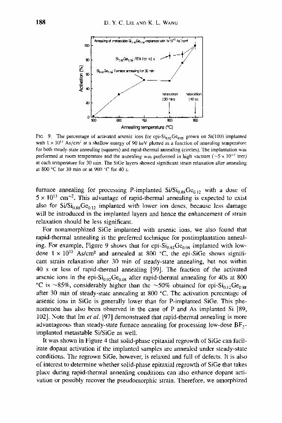
188 D. Y. C. LIE AND K. L. WANG
§ 60
1 5 40
T ' 1 ' 1 ' r-r.—7 r-Annealing of metastable SigggGe joe inplanted wrth 1x10 - AsVcm?
SQ 92Geo Qgi f umace annealing f a 30 min
relaxatbn relaxation
(30 min) (40 s)
600 700 800 900
Annealing temperature ("C)
FIG. 9. The percentage of activated arsenic ions for epi-Sio92Geoo8 grown on Si(lOO) implanted with 1x10'^ As/cm^ at a shallow energy of 90 keV plotted as a function of annealing temperature for both steady-state annealing (squares) and rapid-thermal annealing (circles). The implantation was performed at room temperature and the annealing was performed in high vacuum (-^5 x 10"^ torr) at each temperature for 30 min. The SiGe layers showed significant strain relaxation after annealing at 800 °C for 30 min or at 900 °C for 40 s.
furnace annealing for processing P-implanted Si/Sio88Geoi2 with a dose of 5 X 10 ^ cm"^. This advantage of rapid-thermal annealing is expected to exist also for Si/Sio ggGco 12 implanted with lower ion doses, because less damage will be introduced in the implanted layers and hence the enhancement of strain relaxation should be less significant.
For nonamorphized SiGe implanted with arsenic ions, we also found that rapid-thermal annealing is the preferred technique for postimplantation anneal-ing. For example. Figure 9 shows that for epi-Sig 92Geoo8 implanted with low-dose 1 X 10 ^ As/cm^ and annealed at 800 °C, the epi-SiGe shows signifi-cant strain relaxation after 30 min of steady-state annealing, but not within 40 s or less of rapid-thermal annealing [99]. The fraction of the activated arsenic ions in the epi-Sio 92Geoo8 after rapid-thermal annealing for 40s at 800 °C is --85%, considerably higher than the -^50% obtained for epi-Sig i2Geo 88 after 30 min of steady-state annealing at 800 °C. The activation percentage of arsenic ions in SiGe is generally lower than for P-implanted SiGe. This phe-nomenon has also been observed in the case of P and As implanted Si [89, 102]. Note that Im et al. [97] demonstrated that rapid-thermal annealing is more advantageous than steady-state furnace annealing for processing low-dose BF2-implanted metastable Si/SiGe as well.
It was shown in Figure 4 that solid-phase epitaxial regrowth of SiGe can facil-itate dopant activation if the implanted samples are annealed under steady-state conditions. The regrown SiGe, however, is relaxed and full of defects. It is also of interest to determine whether solid-phase epitaxial regrowth of SiGe that takes place during rapid-thermal annealing conditions can also enhance dopant acti-vation or possibly recover the pseudomorphic strain. Therefore, we amorphized

4 SIGE/SI PROCESSING 189
Si and Sig 92660 og using 20-keV P ions or 90-keV As ions with a common dose of 1.5 X 10 ^ cm~^ and performed rapid-thermal annealing from 600 to 800 °C for 10-40s. Right after completion of solid-phase epitaxial regrowth, the per-centage of activated dopants always lies at 80-100%, which proves that SPE can facilitate dopant activation of P and As ions in SiGe, much as in the cases of bulk Si and Ge, regardless of the annealing technique used [96, 140]. Atz-man et al. [126] also reported that activation of implanted Sb ions in regrown SiGe is significantly better than the cases of nonamorphized SiGe. However, for amorphized SiGe samples, the advantage of rapid-thermal annealing over steady-state annealing no longer exists. The original pseudomorphicity and crys-tallinity of regrown metastable SiGe is always lost after either steady-state fur-nace annealing or rapid-thermal annealing (which is true for at least high-dose B-, Si-, P-, BF2-, Ge-, As-, and Sb-implanted samples) [96, 101, 140]. More studies are, therefore, needed to determine whether rapid-thermal annealing still outperforms furnace annealing under various other implantation conditions.
2.4.3. Issues with Direct Oxidation of SiGe
One important feature of the Si/Si02 system is that thermally grown Si02 can be used as a perfect masking layer where windows can be etched open and junctions are formed by implantation or diffusion of dopants (note that the diffusion coefficients of most dopants in Si02 are smaller than those in Si by several orders of magnitude). To etch the windows open and make planar devices for ICs, the masking material should be insoluble in water, easy to etch, and have very low pinhole density ('^l or less pinhole per wafer). Another salient feature of the Si/Si02 system is that the interface trapping density D^^ and the other oxide traps can be minimized (such as Dj < 5 x 10 ^ cm"^ and the mobile ion charge 2^ < 1 x 10 ^ cm~^) and a high-dielectric breakdown strength >10 MV/cm can be routinely achieved [146-148]. These almost per-fect characteristics of the Si/Si02 system enabled complex planar ICs to be manufactured at low cost and has led to tremendous advances in Si technology over the past 30 years.
As we start to process the Si/SiGe system to make heterojunction devices, we find out immediately that direct thermal oxidation of SiGe ends up with Ge piling up at the interface, messing up the interface properties of the oxide with high Djt and oxide charges [149, 150]. Germanium Oxide is also water soluble, which is not ideal for masking. Patton et al. [149], Nayak et al. [75], and LeGoues et al. [150, 151] all studied direct oxidation of strained SiGe and found that the initial oxidation rate of SiGe is better than in Si, and they proposed different mechanisms on the oxidation kinetics (such as catalytic interaction of Ge with H2O and the presence of Ge-reduced interstitial injection during oxidation). Therefore, for practical purposes, direct thermal oxidation of SiGe should always be avoided by placing a Si cap layer on top of the strained

190 D. Y. C. LIE AND K. L. WANG
SiGe layer [152]. An alternative is to prepare the SiOj film by deposition with the help of microwave electron cyclotron resonance plasma processing, rapid-thermal oxidation, or high-pressure oxidation to alter the oxidation kinetics to realize excellent oxide interface properties [153-155].
2.4.4. Other Practical Process Integration Issues with Si/SiGe
Most of the published Si/SiGe BiCMOS processes adopt the "base = gate" integration scheme, where the base polycrystalline regions of the n-p-n bipolar transistors are patterned at the same time as the MOSFET polycrystalline gate [4, 156]. All devices undergo the same high-temperature rapid-thermal anneal-ing step that activates all dopants [such as after the high-dose extrinsic base linkup implant for HBTs and the gate and Source-to-drain (S-D) implants for MOSFETs]. For this kind of base = gate process, a thin polycrystalline silicon (poly-Si) "protection" layer typically is deposited on the CMOS gate oxide area right after the MOS gate oxidation is done. This poly-Si layer is patterned and removed in the Si/SiGe HBT region and then followed by a low-temperature epitaxy to grow single crystal epibase in the HBT regions and the polycrys-talline materials everywhere else [156]. The MOSFET gate stack, therefore, includes both the initial poly-Si protection layer and the polycrystalline mate-rial deposited by this epibase growth. This kind of integration approach may work fine with 0.5-fim CMOS processes, but can have problems integrating with the advanced sub-0.25-/im CMOS processes. Due to the significant poly-crystalline depletion effects that adversely degrade the device current drive for short-channel MOSFETs, high-temperature rapid-thermal annealing (RTA) typ-ically is required after the S-D implants to activate the dopants. This poly-si depletion issue in nMOS (n^ poly-si) and in pMOS (p^ polycrystals) typically cannot be optimized by a single annealing step. The n+ polycrystals (typically implanted with arsenic or with both arsenic and phosphorus atoms) suffer a more serious polycrystalUne depletion effect and higher annealing temperatures are required to activate the dopants than for the p" polycrystals. However, at high RTA temperatures, two issues arise for pMOS: (1) B penetration from the p+ polycrystals diffusing through the very thin gate oxide (^30 A) cause large threshold voltage variation, large mobility degradation, and possible local cur-rent leakage; (2) B from the S-D p+ implant can diffuse laterally into the channel and shorten the device channel length in a noncontrollable fashion (transient-enhanced diffusion), which drastically increases the device off-state leakage cur-rent. There is obviously a trade-off in the thermal budget for the sub-O.lS-fim MOSFET design between the polycrystalline depletion issues associated with n" gate polycrystals for nMOS and the boron penetration-diffusion problem for pMOS [157].
To reduce the manufacturing and process development costs, a popular approach for IC fabrication is to develop special Si/SiGe BiCMOS processes in

4 SIGE/SI PROCESSING 191
house that can be built on a standard CMOS process developed and acquired from a typical low-cost wafer fabrication foundry. In this case, the required S-D annealing temperature and hot time for the Si/SiGe HBTs are obviously not optimized, even though they may have been painstakingly optimized for the advanced sub-0.25-/xm CMOS processes. Note that because the digital CMOS process is mature and all design libraries, circuits, and products were already developed for the foundry's advanced (but low-cost) CMOS process, one cer-tainly would not want to tamper with the hot time of the foundry's CMOS process. Therefore, the device performance for the Si/SiGe HBTs, which are supposed to provide the highest speed for the critical paths on BiCMOS chips, cannot be optimized without changing the performances of the MOSFETs. To resolve this dilemma for a successful integration of Si/SiGe HBT technology with advanced sub-0.25-)Ltm CMOS processes, a practical approach is to adopt the "base after gate" scheme. A recent article from IBM reported some details of this integration method [158]. The base after gate process typically performs the S-D implant and drive-in annealing for the nMOS first, and then proceeds with the HBT process module. After the HBTs are entirely formed, this base after gate process continues with the pMOS S-D implant and annealing, and then concludes with the salicidation and backend metallization processes. Note that many film stacks are actually deposited during the HBT module process, including deposition of the epibase and the emitter polycrystalline material and deposition of the oxide-nitride-polycrystalline layers during the formation of the extrinsic base. One of the most challenging process integration issue with this base after gate approach is complete removal of these films from the MOS-FET areas so that the unwanted polycrystalline stringers and/or oxide-nitride spacer residuals do not remain on the MOSFET areas [158].
To enable a very robust Si/SiGe HBT process module, simulations must be performed to optimize strain conditions, process flow parameters, and overall device performance carefully. Initially, establishing a thermal budget range and evaluating its impact on overall process parameters as well as device perfor-mance is an important task. Of particular importance is the effect on Ge seg-regation, SiGe interdiffusion, and strain relaxation. It should be recognized that the decision of the thermal budget is most important during process develop-ment because it impacts many critical steps such as gate oxidation, source-drain activation, and device isolation, to name a few [159]. The performance improve-ment needs to be assessed and compared with bulk Si devices. Isolation and salicide modules may need to be specially developed to accommodate the SiGe layers also.
Another important point is that the early work on Si/SiGe HBTs showed that both the collector and the base currents increased significantly when compared with those in Si bipolar junction transistors (BJTs). Undesirable higher base leakage currents of 5-100 times greater than those in Si BJTs were reported [14]. The causes of the high base leakage currents were partly identified as
192 D. Y. C. LIE AND K. L. WANG
being due to the defects at the Si/SiGe interface; later devices no longer exhibit these serious base leakage issues [160].
It is also interesting to note that typically when a pseudomorphically strained SiGe layer is deposited across an entire wafer, the film stack on the active areas (i.e., areas not covered by oxide) consists of (1) an intrinsic Si cap layer, (2) the pseudomorphic SiGe layer (with Ge content ramped or not ramped), and (3) another intrinsic Si layer (or an undoped SiGe strained layer with constant Ge content). This stack lies directly on top of the Si substrate. However, when the epi-SiGe film is deposited over the oxide area, the layer become polycrys-talline and becomes the extrinsic base contact of the Si/SiGe HBT and/or the polycrystalline gate electrode of the CMOS device.
In addition to the issues described in the preceding text (such as thermal bud-get, implantation and annealing, and film removal), many other practical pro-cess integration issues exist for the Si/SiGe BiCMOS processes. Because these issues are highly dependent on device architectures and tool sets, it is impossi-ble to cover all of them here. Harame et al. [4] nicely reviewed several Si/SiGe device architectures in their article, where both non-self-aligned and self-aligned devices are mentioned (the more practical self-aligned device architectures cov-ered in their article include mesalike, epibase before the epibase, epibase after the epibase, and disposable emitter mandrel). In our opinion, many of the pro-cessing integration issues are not too difficult to resolve as long as the device architecture is carefully selected and the process development and transfers to manufacturing are carefully done and planned. Other processing difficulties, such as the need to develop selective poly-SiGe etch with respect to Si or Si02, are not as fundamental as those listed, so they are not discussed further here. The interested reader is referred to [161].
References
1. T. Makimoto, "Symposium on VLSI," 1996, Technical Digest, pp. 6-9. 2. US News and World Report July 31, p. 41 (1995). 3. R. Hull and J. C. Bean, in "Strained-Layer Superlattices: Materials Science and Technology"
(T. P. Pearsall, Ed.), Chap. 1, pp. 1-72. Academic Press, London, 1991. 4. D. L. Harame, J. H. Comfort, J. D. Cressler, E. E Crabbe, J. Y.-C. Sun, B. S. Meyerson, and
T. Tice, IEEE Trans. Electron Devices 42, 469 (1995). 5. E Schaffler, Solid-State Electron. 37, 765 (1994). 6. Y. J. Mii, Y. H. Xie, E. A. Eitzgerald, D. Monroe, P J. Silverman, J. M. Kuo, A. R. Kortan,
E A. Thiel, and B. E. Weir, J. Vac. Sci. TechnoL, B 10, 1807 (1992). 7. U. Konig, A. J. Boers, E Schaffler and E. Kasper, Electron. Lett. 28, 160 (1992). 8. T. P Pearsall, H. Temkin, J. C. Bean, and S. Luryi, IEEE Electron Device Lett. 7, 330 (1986). 9. R. P G. Karunasiri and K. L. Wang, J. Vac. Sci. TechnoL, B 9, 2064 (1991).
10. E. Kasper and E. Schaffler, "Strained-Layer Superlattices: Materials Science and Technology" (T. P Pearsall, Ed.), Vol. 33, Chap. 4. Academic Press, London, 1991.
11. Y H. Xie, E. A. Eitzgerald, D. Monroe, G. P. Watson, and P. J. Silverman, Jpn. J. Appl. Phys. 33, 2372 (1994).

4 SIGE/SI PROCESSING 193
12. M. D. Giles, in "VLSI Technology" (S. M. Sze, Ed.), Chap. 8, p. 370. McGraw-Hill, Singapore, 1988. M. I. Current, I. Yamada, N. W. Cheung, P. L. F. Hemment, and K. J. Reeson, in "Handbook of Ion Implantation Technology" (J. F. Ziegler, Ed.), pp. 363^33. Elsevier Science, Amsterdam, 1992.
13. J. F. Gibbons, Proc. IEEE 60, 1062 (1972). 14. C. A. King, J. L. Hoyt, and J. F. Gibbons, IEEE Trans. Electron Devices 36, 2093 (1989). 15. P S. Peercy, B. W. Dodson, J. Y. Tsao, E. D. Jones, D. R. Myers, T. E. Zipperian,
L. R. Dawson, R. M. Biefeld, J. F Klem, and C. R. Hills, IEEE Electron Devices Lett. 9, 621 (1988).
16. R. Hull, J. C. Bean, J. M. Bonar, G S. Higashi, K. T. Short, H. Temkin, and A. E. White, Appl. Phys. Lett 56, 2445 (1990).
17. J. S. Kline, R H. Pollak, and M. J. Cardona, Helv Phys. Acta 41, 968 (1968). 18. M. Gell, Phys. Rev. B 38, 7535 (1988). 19. C. G. Van de Walle and R. M. Martin, Phys. Rev B 34, 5621 (1986). 20. S. C. Jain and W. Hayes, Semicond. Sci. Technol. 6, 547 (1991). 21. R. People and J. C. Bean, Appl. Phys. Lett. 48, 538 (1986). 22. J. Del Alamo, S. Swirhun, and R. M. Swanson, "International Electron Device Meeting,"
1985, Technical Digest, p. 290. 23. J. Baslev, Phys. Rev. 143, 636 (1966). 24. B. S. Meyerson, Proc. IEEE 80, 1592 (1992). 25. B. S. Meyerson, Appl. Phys. Lett. 48, 797 (1986). 26. B. S. Meyerson, F J. Himpsel, and K. J. Uram, Appl Phys. Lett. 57, 1034 (1990). 27. S. S. Iyer, in "Epitaxial Silicon Technology" (B. J. Baliga, Ed.), pp. 97-175. Academic Press,
New York, 1985. 28. A. Y Cho, Thin Solid Films 100, 291 (1983). 29. Y Ota, / Appl. Phys. 51, 1102 (1980). 30. J. C. Bean and E. A. Sadowski, /. Vac. Sci. Technol. 20, 137 (1982). 31. H. Kibbel, E. Kasper, P Narozny, and H.-U. Schreiber, Thin Solid Films 184, 163 (1990). 32. E. Kasper and J. C. Bean, Eds., "Silicon Molecular Beam Epitaxy." CRC Press, Boca Raton,
FL, 1988. 33. K. N. Tu, J. W. Mayer, and L. C. Feldman, "Electronic Thin Film Science." Macmillian,
New York, 1992. 34. S. S. Iyer, M. Arienzo, and E. de Fresart, Appl. Phys. 57, 893 (1990). 35. C. A. King, J. L. Hoyt, D. B. Noble, C. M. Gronet, J. F Gibbons, M. P Scott, T. I. Kamins,
and S. T. Laderman, IEEE Electron Device Lett. 10, 159 (1989). 36. J. C. Sturm, E. J. Prinz, and C. W. Magee, IEEE Electron Device Lett. 12, 303 (1991). 37. A. Vollmer, Electronic Design, Jan. 23 (1998). 38. M. Hong, E. de Fresart, J. Steele, A. Zlotnicka, C. Stein, G Tam, M. Racanelli, L. Knoch,
Y C. See, and K. Evans, IEEE Electron Device Lett. 14, 450 (1993). 39. T. F Meister, H. Schafer, M. Franosch, W. Molzer, K. Aufinger, U. Scheler, C. Walz, M. Stolz,
S. Boguth, and J. Bock, "International Electron Device Meeting," 1995, Technical Digest, p. 739. IEEE, New York, 1995.
40. A. Monroy, M. Laurens, M. Marty, D. Dutartre, D. Gloria, J. L. Carbonero, A. Perrotin, M. Roche, and A. Chantre, BCTM, 1999, Technical Digest, p. 121. IEEE, New York, 1999.
41. J. W. Matthews and A. E. Blakeslee, J. Cryst. Growth 27, 118 (1974). 42. J. W. Matthews and A. E. Blakeslee, / Cryst. Growth 29, 273 (1975). 43. Van der Merwe, Surf. Sci. 31, 198 (1972). 44. E. Kasper, Surf. Sci. 174, 630 (1986). 45. J. P Hirth and J. Lothe, "Theory of Dislocations," Chap. 2. McGraw-Hill, New York, 1969. 46. E. Kasper and H. J. Herzog, Thin Solid Films 44, 357 (1977). 47. J. W. Matthews, in "Epitaxial Growth" (J. W. Matthews, Ed.), Chap. 8. Academic Press,
New York, 1975.

194 D. Y. C. LIE AND K. L. WANG
48. J. Willis, S. C. Jain, and R. Bullough, Philos. Mag. A 62, 115 (1990). 49. R. People, IEEE J. Quantum Electron. QE-22, 1696 (1986). 50. D. N. Theodore, G. Tarn, J. Whitefield, J. Christiansen, and J. Steele, Mater. Res. Soc. Symp.
Proc. 319, 159 (1994). 51. D. N. Theodore and G. Tarn, Microscopy Soc. Amer Proc. 1112 (1993). 52. J. M. Baribeau, T. E. Jackman, D. C. Houghton, R Maigne, and M. W. Denhoff, /. Appl
Phys. 63, 5738 (1988). 53. E. A. Fitzgerald, Mater Sci. Rep. 7, 81 (1991). 54. V. S. Sperioso, J. Appl. Phys. 52, 6094 (1981). 55. S. T. Picraux, B. L. Doyle, and J. Y. Tsao, "Strained-Layer Superiattices: Materials Science
and Technology" (T. R Pearsall, Ed.), Vol. 33, Chap. 3, pp. 139-222. Academic Press, London, 1991.
56. T. Vreeland, Jr., and B. M. Paine, J. Vac. Sci. Technol, A 4, 3153 (1986). 57. C. Kittel, "Introduction to Solid State Physics," 7th ed. Wiley, New York, 1996. 58. D. A. Neumann, H. Zabel, and H. Morkoc, Mater Res. Soc. Symp. Proc. 37, 47 (1985). 59. C. R. Wie, T. A. Tombrello, and T. Vreeland, Jr., J. Appl. Phys. 59, 3743 (1986). 60. C. J. Tsai, A. Dommann, M.-A. Nicolet, and T. Vreeland, Jr., J. Appl. Phys. 69, 2076 (1991). 61. G. Bai and M.-A. Nicolet, / Appl. Phys. 70, 649 (1991). 62. D. Y. C. Lie, J. H. Song, N. D. Theodore, A. Vantomme, M.-A. Nicolet, T. K. Cams, and
K. L. Wang, / Appl. Phys. 11, 2329 (1995). 63. R R Fewster, J. Appl. Crystallogr 25, 714 (1992). 64. B. K. Tanner, "X-ray Diffraction Topography," Pergamon, Oxford, 1976. 65. W. K. Chu, J. W Mayer, and M.-A. Nicolet, "Backscattering Spectrometry," Chap. 8,
pp. 223-275. Academic Press, New York, 1978. 66. L. C. Feldman, J. W. Mayer, and S. T. Picraux, "Materials Analysis by Ion Channeling."
Academic Press, London, 1982. 67. F Eisen, in "Channeling: Theory, Observation and Applications" (D. V. Morgan, Ed.),
Chap. 14, p. 426. Wiley, London, 1973. 68. F Cedeira, A. Pinczuk, J. C. Bean, B. Batlogg, and B. A. Wilson, Appl. Phys. Lett. 45, 1138
(1984). 69. G. Bai and M.-A. Nicolet, J. Appl. Phys. 70, 3551 (1991). 70. J. W Edington, "Practical Electron Microscopy in Materials Science." Philips, Eindhoven,
1974. 71. S. M. Sze, "Physics of Semiconductor Devices," 2nd ed. Wiley, New York, 1981. 72. M. Arienzo, S. S. Iyer, B. S. Meyerson, G. L. Patton, and J. M. C. Stork, Appl. Surf. Sci.
48/49, 377 (1991). 73. V. Venkartaraman, C. W. Liu, and J. C. Sturm, Appl. Phys. Lett. 63, 2795 (1993). 74. J. Welser, J. L. Hoyt, and J. F. Gibbons, "International Electron Device Meeting," 1992,
Technical Digest, p. 1000. IEEE, New York, 1992. 75. D. K. Nayak, J. C. S. Woo, J. S. Park, K. L. Wang, and K. R MacWilliams, Appl. Phys. Lett.
62, 2853 (1993). 76. M. Glicksman, Phys. Rev. I l l , 125 (1958). 77. Y C. Chen, S. H. Li, R K. Bhattacharya, J. Singh, and J. M. Hinckley, Appl. Phys. Lett. 64,
3110(1994). 78. G. Busch and O. Vogt, Helv. Phys. Acta 33, 437 (1960). 79. J. M. McGregor, T. Manku, J. R Noel, D. J. Roulston, A. Nathan, and D. C. Houghton,
J. Electron. Mater 22, 319 (1993). 80. S. K. Chun and K. L. Wang, IEEE Trans. Electron Devices 39, 2153 (1992). 81. T. Manku and A. Nathan, IEEE Electron Device Lett. 12, 704 (1991). 82. J. M. Hinckley and J. Singh, Phys. Rev. B4\, 2912 (1990). 83. T. K. Cams, S. K. Chun, M. O. Tanner, K. L. Wang, T. I. Kamins, J. E. Tumer, D. Y C. Lie,
M.-A. Nicolet, and R. G. Wilson, IEEE Trans. Electron Devices 41, 1273 (1994).

4 SIGE/SI PROCESSING 195
84. K. Hess, "Advanced Theory of Semiconductor Devices," Chaps. 8 and 9. Prentice-Hall, Englewood Cliffs, NJ, 1988.
85. P. M. Asbeck, in "Modem Semiconductor Device Physics" (S. M. Sze, Ed.), Chap. 1, p. 47. Wiley, New York, 1998.
86. D. K. Nayak and S. K. Chun, Appl. Phys. Lett. 64, 2514 (1994). 87. D. Rosenfeld and S. A. Alterovitz, IEEE Trans. Electron Devices 41, 848 (1994). 88. M. M. Rieger and P Vogl, Phys. Rev. B 48, 14276 (1993). 89. J. Gyulai, in "Ion implantation: Science and Technology" (J. F. Ziegler, Ed.), pp. 139-210.
Academic Press, Orlando, 1984. 90. L. J. van der Pauw, Philips Tech. Rev 20, 220 (1958). 91. N. G. E. Johansson, J. W. Mayer, and O. J. Marsh, Solid State Electron. 13, 317 (1970). 92. D. Y. C. Lie, J. Electron. Mater. 27, 377 (1998). 93. Fisful, "Heavily Doped Semiconductors," p. 133, Plenum Press, New York, 1969. 94. D. Y C. Lie, N. D. Theodore, and J. H. Song, Appl. Surf. Sci. 92, 557 (1996). 95. D. Y C. Lie, J. H. Song, M.-A. Nicolet, and N. D. Theodore, J. Electron. Mater 25, 87 (1996). 96. D. Y C. Lie, J. H. Song, M.-A. Nicolet, N. D. Theodore, M. O. Tanner, S. Thomas, and
K. L. Wang, J. Appl. Phys. 79, 8341 (1996). 97. S. Im, F. Eisen, M.-A. Nicolet, M. O. Tanner, K. L. Wang, and N. D. Theodore, J. Appl. Phys.
81, 1695 (1997). 98. D. Y C. Lie, J. H. Song, M.-A. Nicolet, and N. D. Theodore, Appl. Phys. Lett. 66, 592 (1995). 99. S. Im, D. Y C. Lie, and M.-A. Nicolet, J. Appl. Phys. 79, 7389 (1996).
100. Z. Atzman, M. Eisenberg, P. Revesz, J. W. Mayer, S. Q. Hong, and F. Schaffer, Appl. Phys. Lett. 60, 2243 (1992).
101. L. Eriksson, J. A. Davies, N. G. E. Johassson, and J. W. Mayer, J. Appl. Phys. 40, 842 (1969). 102. J. W. Mayer, L. Eriksson, and J. A Davis, "Ion Implantation in Semiconductors." Academic
Press, New York, 1970. 103. G. L. Olson and J. A. Roth, Mater Sci. Rep. 3, 1 (1988). 104. J. S. Williams in "Surface Modification and Alloying" (J. M. Poate and G. Foti, Eds.). Plenum,
New York, 1983. 105. E. P. Donovan, F. Spaepen, D. Tumbull, J. M. Poate, and D. C. Jacobson, / Appl. Phys. 57,
1795 (1985). 106. D. C. Paine, J. Miner Metal. Mater Soc. 2, 55 (1993). 107. L. Csepregi, J. W. Mayer, and T W Sigmon, Phys. Lett. A 54, 157 (1975). 108. I. Suni, G. Goltz, M.-A. Nicolet, and S. S. Lau, Thin Solid Film 93, 171 (1982). 109. E Spaepen, Acta Metall. Mater 26, 1167 (1978). 110. T. Saito and I. Ohdomari, Philos. Mag. B 43, 673 (1981). 111. S. S. Lau and W. F. Van der Weg, "Thin Films: Interdiffusion and Reactions" (J. M. Poate,
K. N. Tu, and J. W. Mayer, Eds.), Chap. 12. Wiley-Interscience, New York, 1978. 112. P. J. Germain, M. A. Paesler, D. E. Sayers, and K. Zellama, Mater Res. Soc. Symp. Proc. 13,
135 (1983). 113. J. Narayan, J. Appl. Phys. 53, 8607 (1982). 114. I. Suni, G. Goltz, M. G. Grimaldi, M.-A. Nicolet, and S. S. Lau, Appl Phys. Lett. 40, 269
(1982). 115. A. Lietolia, A. Wakita, T W. Sigmon, and J. R Gibbons, / Appl. Phys. 53, 4399 (1982). 116. J. M. Poate and J. S. Williams, "Ion Implantation and Beam Processing," pp. 13-57. Academic
Press, New York, 1984. 117. M. J. Aziz, Mater Res. Soc. Symp. Proc. 321, 1, (1994). 118. G.-Q. Lu, E. Nygren and M. J. Aziz, J. Appl. Phys. 70, 5323 (1991). 119. P Kringh0j and R. G. Elliman, Phys. Rev Lett. 73, 858 (1994). 120. D. C. Paine, N. D. Evans, and N. G. Stoffel, J. Appl. Phys. 70, 4278 (1991). 121. S. Q. Hong, Q. Z. Hong, and J. W. Mayer, J. Appl. Phys. 72, 3821 (1993). 122. D. Y C. Lie, N. D. Theodore, J. H. Song, and M.-A. Nicolet, J. Appl. Phys. 11, 5160 (1995).

196 D. Y. C. LIE AND K. L. WANG
123. D. Y. C. Lie, T. K. Cams, N. D. Theodore, F. Eisen, M.-A. Nicolet, and K. L. Wang, Mater. Res. Soc. Symp. Proc. 321, 485 (1994).
124. Q. Z. Hong, J. G. Zhu, J. W. Mayer, W. Xia, and S. S. Lau, J. Appl. Phys. 71, 1768 (1992). 125. C. Lee, T. E. Haynes, and K. S. Jones, Appl. Phys. Lett. 62, 501 (1993). 126. Z. Atzman, M. Eisenberg, Y Shacham-Diamand, J. W. Mayer, and F. Schaffler, J. Appl. Phys.
75, 377 (1994). 127. T. E. Haynes, M. J. Antonell, C. A. Lee, and K. S. Jones, Phys. Rev. B 51, 7762 (1995). 128. B. T. Chilton, B. J. Robinson, D. A. Thompson, T. E. Jackman, and J.-M. Baribeau, Appl
Phys. Lett. 54, 2 (1989). 129. M. J. Aziz, P. C. Sabin, and G.-Q. Lu, Phys. Rev. 5 44, 9812 (1991). 130. G.-Q. Lu, E. Nygren, M. J. Aziz, D. Tumbull, and C. W. White, Appl. Phys. Lett. 54, 2583
(1989). 131. J. Fratello, J. F. Hays, and D. Tumbull, J. Appl. Phys. 51, 4718 (1980). 132. D. Y C. Lie, A. Vantomme, R Eisen, T. Vreeland, Jr., M.-A. Nicolet, T. K. Cams, and
K. L. Wang, J. Appl. Phys. 14, 6039 (1993). 133. P. Kringh0j, R. G. Elliman, and J. L. Hansen, Mater. Res. Soc. Symp. Proc. 321, 461 (1994). 134. R. G. Elliman, W.-C. Wong, and P Kringh0j, Mater. Res. Soc. Symp. Proc. 321, 375 (1994). 135. D. C. Paine, D. J. Howard, N. G. Stoffel, and J. H. Horton, J. Mater. Res. 5, 1023 (1990). 136. D. C. Paine, D. J. Howard, and N. G. Stoffel, J. Electron. Mater. 20, 735 (1991). 137. D. J. Howard, W. E. Bailey, and D. C. Paine, Appl. Phys. Lett. 63, 2893 (1993). 138. W.-C. Wong and R. G. Elliman, Mater Res. Soc. Symp. Proc. 321, 491 (1994). 139. M. G. Grimaldi, B. M. Paine, M.-A. Nicolet, and D. K. Sadana, J. Appl. Phys. 52, 4038
(1981). 140. D. Y C. Lie, S. Im, and J. H. Song, unpublished data. 141. D. Y C. Lie, N. D. Theodore, J. Steele, and T. C. Smith, U.S. Patent 5,565,690, 1996. 142. D. K. Nayak, K. Kamjoo, J. S. Park, J. C. S. Woo, and K. L. Wang, IEEE Trans. Electron
Devices 39, 56 (1992). 143. D. J. Eaglesham, J. M. Poate, D. C. Jacobson, M. Cemllo, L. N. Pfeiffer, and K. West, Appl.
Phys. Lett. 58, 523 (1991). 144. J. Klappe, Ph.D. Thesis, University of Twente, Netherlands, 1994. 145. T. O. Sedgwick, Mater Res. Soc. Symp. Proc. 92, 3 (1987). 146. B. E. Deal and A. S. Grove, J. Appl. Phys. 36, 3770 (1965). 147. E. H. Nicollian and J. R. Brews, "MOS Physics and Technology." Wiley, New York, 1982. 148. P Balk, Ed., "The Si-SiOj System." Elsevier, Amsterdam, 1998. 149. G. L. Patton, S. S. Iyer, S. L. Delage, E. Ganin, and R. C. Mcintosh, Mater Res. Soc. Symp.
Proc. 102, 295 (1988). 150. F. K. LeGoues, R. Rosenberg, T. Nguyen, F. Himpsel, and B. S. Meyersen, J. Appl. Phys. 65,
1724 (1989). 151. F. K. LeGoues, R. Rosenberg, and B. S. Meyerson, / Appl. Phys. 65, 1724 (1989). 152. D. K. Nayak, K. Kamjoo, J. S. Park, J. C. S. Woo, K. L. Wang, and K. P MacWilUams, IEEE
Electron Device Lett. 12, 154 (1991). 153. S. S. Iyer, R M. Solomon, V. P Kesan, A. A. Bright, J. L. Freeouf, T. N. Nguyen, and
A. C. Warren, IEEE Electron Device Lett. 12, 246 (1991). 154. R M. Garone, V. Vekatarrman, and J. C. Sturm, IEEE Electron Device Lett. 12, 230 (1991). 155. R W. Li, E. Yang, Y Yang, J. Chu, and B. Meyerson, IEEE Electron Device Lett. 15, 402
(1994). 156. D. Nguyen-Ngoc, D. L. Harame, J. C. Malinowski, S. J. Jeng, K. T. Schonenberg,
M. M. Gilbert, G. D. Bert, M. Soyuer, K. A. Tallman, K. J. Stein, R. A. Groves, S. Subbanna, D. B. Colavito, D. A. Sunderiand, and B. S. Meyerson, BCTM, Technical Digest, pp. 89-92. IEEE, New York, 1995.
157. A. Hon, H. Umimoto, H. Nakaoka, M. Sekiguchi, and M. Segawa, "Intemational Electron Device Meeting," Technical Digest, p. 575. IEEE, New York, 1996.

4 SIGE/SI PROCESSING 197
158. S. A. St. Ogne, D. L. Harame, J. S. Dunn, S. Subbanna, D. C. Ahlgren, G. Freeman, B. Jagannathan, S. J. Jeng, K. Schonenberg, K. Stein, R. Grives, D. Coolbaugh, N. Feilchenfeld, P. Geiss, M. Gordon, P. Gray, D. Hershberger, S. Kilpatrick, R. Johnson, A. Joseph, L. Lanzerotti, J. Mahnowski, B. Omer, and M. Zierak, BCTM, Technical Digest, p. 117. IEEE, New York, 1999.
159. M. Racanelli, Z. Zhang, J. Zheng, A. Kar-Roy, P Joshi, A. Kalburge, L. Nathawad, M. Todd, C. Ukah, C. Hu, C. Compton, K. Schuefraf, P Ye, R. Dowlatshahi, G. Jolly, and P Kempf, BCTM, Technical Digest, p. 125. IEEE, New York, 1999.
160. J. D. Cressler, BCTM Short Course. IEEE, New York, 1999. 161. R Scott Johnson, J. Electron. Mater. 21, 805 (1992).

This Page Intentionally Left Blank

SEMICONDUCTORS AND SEMIMETALS, VOL. 73
CHAPTER 5
Advances in Quantum Dot Structures
S. Kim and M. Razeghi
CENTER FOR QUANTUM DEVICES, ELECTRICAL AND COMPUTER ENGINEERING DEPARTMENT,
NORTHWESTERN UNIVERSITY, EVANSTON, ILLINOIS, USA
1. INTRODUCTION 199
2. PHYSICAL PROPERTIES 201
2.1. Density of States 201 2.2. Energy States 202 2.3. Optical Absorption and Transition in Quantum Dots 204 2.4. Devices Based on Zero-Dimensional Quantum Structure 207
3. STATE OF THE ART 209
REFERENCES 212
1. Introduction
Semiconductor quantum dots (QDs) represent one of the rigorous ongoing research areas for next generation optoelectronic devices. The strong interest in low-dimensional semiconductor structures originates from their exciting elec-tronic properties that have an important impact on the performance of high-speed electronic and photonic devices and, moreover, on the development of novel device concepts such as the single electron transistor. The quantum dots known as quantum boxes are nanometer-scale islands in which electrons and holes are confined in three-dimensional potential boxes. They are expected to exhibit a zero-dimensional, S-function density of states and are able to quan-tize electrons free motion by trapping it in a quasi-zero-dimensional potential confinement. Due to these peculiar characteristics, quantum dots are expected to have superior characteristics for device performance in semiconductor lasers, detectors, and modulators.
The condition for new electronic properties to occur in such device structures is that the lateral size of their active region must be smaller than the coherence length and the elastic scattering length of the carriers. Additional quantum-size effects require the structural features to be reduced to below 50 nm, that is, the range of the de Broglie wavelength. Therefore, the reproducible fabrica-tion of these nanometer-scale quantum structures requires methods with atomic
199 Copyright © 2001 by Academic Press
All rights of reproduction in any form reserved. ISBN 0-12-752182-8
ISSN 0080-8784/01 $35.00
200 S. KIM AND M. RAZEGHI
scale precision, which is a major challenge for today's microstructure materials science.
As a result of the strong confinement imposed in all three spatial dimensions, quantum dots are similar to atoms. They are frequently referred to as artifi-cial atoms, superatoms, or quantum dot atoms [1]. What makes quantum dots such unusual objects is, first of all, the possibility to control their shape, their dimensions, the structure of energy levels, and the number of confined elec-trons. It is possible, for instance, to create and investigate, as a rectangular or parabolic potential well binding, one or several particles, as well as the Landau quantization of motion of a single electron, the radiative recombination from a few-particle system, and so on.
Quantum dots were first realized by scientists from Texas Instruments Incor-porated. Reed et al. reported the creation of a square quantum dot with a side length of 250 nm, etched by means of lithography. Since then, quantum dot and quantum wire structures have been fabricated by means of subsequent lat-eral patterning of two-dimensional heterostructures with lithographic techniques followed by chemical etching or selective crystal growth on prepattemed and masked substrates. However, although many fundamental properties of low-dimensional semiconductors can be demonstrated in these structures, it turns out that lithographic patterning processes and chemical etching always intro-duce defects that degrade the crystal quality and cause irregularities in size and shape of the quantum structures that are detrimental for practical applications in semiconductor devices. Especially to reduce the defect density, several meth-ods for the direct fabrication of quantum dots and quantum wires based on the epitaxial growth process itself have been exploited. Quantum dots and wires have been grown by using the periodic step structure on vicinal surfaces, the generation of supersteps, and the breakup of high index surfaces into arrays of nanometer-scale facets.
Recently, first breakthrough for growth of high quality highly strained epitax-ial layers since the Stranski-Krastanow growth mode [2] was rediscovered dur-ing highly strained layer epitaxy; it is called self-assembled quantum dots. This discovery has great meaning for a new era of optoelectronic devices, providing new techniques for low-dimensional quantum structure [3-5]. When the lattice constants of the substrate and the crystallized material differ considerably, only the first deposited monolayer crystallizes in the form of epitaxial strained lay-ers, where the lattice constant is equal to that of the substrate. When the critical thickness is exceeded, a significant strain that occurs in the layer leads to the breakdown of this ordered structure and to the spontaneous creation of randomly distributed islets of regular shape and similar sizes [6]. The small sizes of the self-assembled quantum dots (diameters in the range of 30 nm or even smaller), the homogeneity of their shapes and sizes in a macroscopic sample, the perfect crystal structure (without edge defects), and the fairly convenient growth pro-cess, without the necessity to precisely deposit electrodes or etching, are among their greatest advantages. Thus there is great hope with regard to their future applications in electronics and optoelectronics.

5 ADVANCES IN QUANTUM DOT STRUCTURES 201
2. Physical Properties
2.1. DENSITY OF STATES
Quantum confinement of charge carriers in semiconductors takes place when the carriers are trapped within potential wells of sufficiendy small dimensions. This quantum confinement can give rise to significant modification of the energy band structure and density of states (DOS) distribution in these materials. In the discussion that follows, we treat the quantum-confined structure in a simple, single-band model. Although this picture is adequate for the conduction band case, more elaborate multiband models, including the effect of band mixing, have been developed for the valence band.
In the effective mass approximation, the energy spectrum E of the carriers is obtained by solving Schrodinger's equation
2
.^y^V{x.y^z) ^{x.y.z) = E^{x,y,z)
where "^ is the carrier envelope wave function, nf is the carrier effective mass, and y(jc, y, z) is the potential distribution. For potential wells of rectangular shape, one-, two-, and three-dimensional quantum confinement can be achieved in film-, wire-, and boxlike geometries by successively reducing the well dimen-sions r , ty, and t^. For infinitely deep potential wells, the energy of the confined carriers (with respect to the band edge) is given by
' lm*tl 2m*
one-dimensional (ID) confinement
n* \tl t] ) Ei.n. = ^r-\-^ + -r\ + 2m* \tl tl I 2m*
two-dimensional (2D) confinement s2^2 / /2 ^ 2 ^2^
three-dimensional (3D) confinement
where /, m, n = 1, 2 , . . . are the level quantum numbers and ky, k^ are the wave vector components along the unconfined dimensions. Quantum confinement in such quantum well (QWL), quantum wire (QWR), or quantum dot (QD) struc-tures thus results in charge carriers of a quasi-2D, ID, or zero-dimensional (OD) nature.

202 S. KIM AND M. RAZEGHI
The density of states functions, including spin degeneracy, are given by
P3D = ^^-^ V £ 27r2
P2D
PlD
POD
(2m*)
E0(^-^/) X I
*V/2
X y I, m
EiE-Ei,J -1/2
X y z l,m,n
J:HE-E,„J
for 3D, quasi-2D, ID, and OD carriers, respectively. S{x) is the Heaviside function: ^ = 0 for jc < 0; ^ = 1 for jc > 0. The DOS distributions (Fig. 1) acquire sharper features as the carrier dimensionality is reduced, particularly in the case of ID and OD structures. Note, however, that these sharp features can be significandy smoothed out by well size fluctuations, leading to inhomogeneous broadening of the energy spectrum.
2.2. ENERGY STATES
To explain three-dimensional quantum confinement, the quantum mechani-cal problem of the motion of a particle in a box was recalled. This problem turned out to be very complicated, because all the possibilities of electron-hole Coulomb interaction—valence band structure or nonparabolic bands—were considered.
>
0 Q
3D 2D A
• L
ID
y ^
>
— >
\ )D
— > •
El E2 Ell ^12 Ei3
FIG. 1. Density of States.
b j i r, 11 ^21 ^11 ^21

5 ADVANCES IN QUANTUM DOT STRUCTURES 203
The total Hamiltonian H for an electron-hole pair in the QD is given by
^h,kinVh) — ^ T V.—i—v. + v — i — V
-e^ 1
where ^ jcin and ///j^in are the kinetic energy of electrons and holes, and V and Vyj are the potential energy of electrons and holes, respectively. The H^ is the Coulomb interaction term, which is the only term dependent on coordinates of both electrons and holes, and couples of their motion. In spherical quantum dots, taking into account the Coulomb potential, there is a break in symme-try, because the Coulomb interaction depends on the spatial distance between the electrons and the holes. The simplest approach takes into account that the Coulomb energy scales like the inverse of the electron-hole distance (~ 1//^), whereas the kinetic energy scales like the square of the inverse radius (~ l/R^)-One possible description for small dot radii in the so-called strong confinement range (R <^ag, where a^ is the excitonic Bohr radius) [7] is the neglect of all Coulomb interaction effects. Even the Coulombic effect cannot be completely neglected, and it is solved by numerically using the perturbation theory.
To solve the hole energy states, more complicate models for the kinetic energy term of the hole H^^ have been introduced in the Hamiltonian. The hole Hamiltonian H^ can be expressed for cubic materials with strong spin-orbit coupling by
- —[lp.p,WM + ip,p.WAl + tp.pMV-.)] niQ
where JTIQ is the electron mass, 7i,72'73 are the parameters introduced to describe the valence band dispersion, P is the hole momentum operator, and J is the 3/2 angular momentum operator.
The preceding expression can be simplified by considering the spherical symmetry. Small contributions of terms of cubic or hexagonal symmetry are neglected and parameter m is introduced to give the strength of spherical spin-orbit interaction. This can be described as
2mo p2_^(p(2)j(2))

204 S. KIM AND M. RAZEGHI
where the coupling parameter m is defined by
673+472 M =
57,
The involvement of the full valence band structure results in a qualitative new description of the electron and hole energy states (Fig. 2).
2.3. OPTICAL ABSORPTION AND TRANSITION IN
QUANTUM DOTS
2.3.L Absorption Coefficients
We consider the absorption coefficient of an ensemble of quantum dots
1 C , ^ 4 7 7 , 1 C 477
«av(w) = — / dR—R'P{R)a^^{(o, R)
which is one of the important optical properties. The averaged absorption spec-trum aav(^) c^^ ^^ expressed by
1 C 477
«ave = TT / dR—R'PiR)aQ^ico, R)
where VQD is the average quantum dot volume, R is the radius, P{R) is a char-acteristic distribution function for the dot sizes, and aQ^{(x), R) is the absorption coefficient of a single quantum dot. The absorption spectrum is given by a series of Lorentzian lines for the ground and excited states at energies £QD = hoj^, with homogeneous line widths Yj and oscillator strengths ff.
To solve these two equations, we need information about the radius R and the size distribution P(K), and we need to determine suitable relationships for the size dependence of energy E{K), homogeneous line broadening r(/?), and oscillator strength /(/?).
23.2. Absorption Process
To discuss the optical absorption spectrum a(a)) of a quantum dot, the proba-bility for the dipole allowed optical transitions between single electron and hole states has to be evaluated. According to a simplified model, the most important optical transitions between electron and hole states are Is^ ^- 1 ; , Ipe -> IPh^

5 ADVANCES IN QUANTUM DOT STRUCTURES 205
70%
without Piezoelectric Potential
1 d ^ ^ ^
* ^ i ^
12nm (a)
" . . . |ioo> —ig^N,
LF!:
1110)
with Piezoetectric Potential
(b)
FIG. 2. Energy state of the InAs QDs in GaAs. Reprinted with permission from [8].

206 S. KIM AND M. RAZEGHI
IE electron states I P
IS.
AE
hole states
l(S,D)3^1(P,F)3„ • 2(S,D)3^ • 3(S,D)3^
2(P-F)3,
1S„
-TT-
;; *^ i
1
, 1
^ I I •
1 : I i III ; : i i
r ' 1 ; A
1
1 i ) r
3 f groi
'. .T. y.
two-pair s
-lSel(P,F)3/2
ls,l(S,D)
ls,l(P,F)
ls,l(S,D)
one-pair s
IPe 1(P,F
ls^2(S,D
ls,l(S,D
FIG. 3. Simplified scheme of the optical transitions plotted for a quantum dot in the strong con-finement regime (a) in the picture of independent electron and hole states and (b) in the one-pair and two-pair picture and considering Coulomb effect. Reprinted with permission from [9].
and so forth. For an optical transition within the ladder of either an electron or hole state (m^raband transition), we obtain the selection rules rif / n^, If — l^ = 0, ±1 , and mf — nii = 0, ±1 .
Next, we briefly describe the possible optical transition between the calcu-lated QD energy states. Valence band coupling gives rise to formerly forbidden optical transitions between electron and hole states with An ^0 and signifi-cant oscillator strength is acquired. In Figure 3a, we illustrate the energy label scheme for the energetically lowest electron and hole states and the allowed optical transition between them. The relevance for the nonlinear spectra is illus-trated as a one-pair-two-pair picture in Figure 3b. Transitions 1 and 2 are the same as the dominant one-pair transition between s- and p-type electron and holes; transition 3 is the somewhat weaker one-pair transition with the hole in the first excited state. For the two-pair states in three dimensionally confined quantum dots, the theory predicts (i) a large binding energy, (ii) observation of both ground and excited two-pair states in the optical spectra because of the absence of the typical 3D continuum states, and (iii) transitions to excited two-pair states that originally were forbidden and now occur due to the change of selection rules caused by the Coulomb potential.
The existence of the two-pair states is important for the interpretation of differential absorption spectra. After population of the one-pair states by pump photons, the pair states can be populated by an photon absorption process. Then induced absorption is energetically low compared to the one-pair energy that appears in the spectrum due to the transition to the two-pair ground state. These transitions are only possible because the Coulomb interaction has changed the selection rules.

5 ADVANCES IN QUANTUM DOT STRUCTURES 207
2.4. DEVICES BASED ON ZERO-DIMENSIONAL QUANTUM STRUCTURE
2.4.1. ID and OD Electronic Devices
Rapid progress in fabrication technology and well controlled growth results are being realized for nanostructure quantum devices for future applications. The ultrasmall structure concept for speed and integration is clearcut and fol-lows the mainstream approach to very large and ultra-large scale integration. Within this natural trend, quantum devices are just the result of the evolution of lithography. Whereas deterministic, zero defect interconnections seem out of reach to conserve reasonable fabrication yields, the error margins will decrease due to increased fluctuations, such as diminished carrier numbers for logic oper-ation, or fabrication tolerances.
Granular electronics are highly desirable devices, because single or a few electrons are used to perform digital operations instead of our present-day, well-known transistors that operate at best with = 10" electrons. Such devices are based on concepts similar to the Coulomb blockade concept, where the single electron charge changes a local potential energy in a structure by ^V = e/C, where C is a local capacitance, determined by the device geometry and mate-rials. The Coulomb blockade effect [10, 11] has been the subject of many investigations in the context of small, superconducting tunnel junctions at low temperatures and can be shown to allow digital electronic functions when several devices are combined. A recent implementation demonstrates a turnstile device activated by alternating gate voltages. Future issues are the demonstration of high-temperature, error-free devices (i.e., device energy e^/C much higher than operating thermal energy k^T), and circuit and systems architecture, including interconnections, and self-repair.
Recent progress in ballistic deterministic motion [12] indicates that many large, interesting effects can be obtained in a nonquantized, classical situation where electrons travel without collisions. Some effects occur in unquantized modes, such as those due to coherent focussing effects or lateral hot-electron devices. Analog steering of an electron beam into spatially arranged collec-tor electrodes through electrostatic lenses or split gates might allow analog-to-digital conversion in the multi-gigahertz range. The ballistic electron device would be used as the critical element of the converter, and connections to the outside world would be made through standard devices, achieving an integrated electrooptics component. A tunneling hot-electron transfer amplifier could also be realized in the 2D electron gas plane thanks to narrow metal gates (^ 50 nm).
Cellular automata machines [13, 14] (see Fig. 4), which consist of arrays of elementary digital processors that are located at the nodes of a regular lat-tice and are connected to a few neighbors, can be revolutionary, fault-tolerant architectures at low dimensions to alleviate difficulties associated with nonde-terministic modes of operation of tens or hundreds of millions of integrated transistors. The processors can be as simple as logic gates, but can also be full
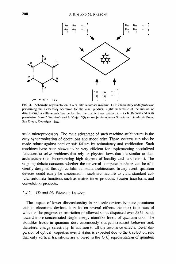
208 S. KIM AND M. RAZEGHI
a i l
All
ai2
322
c<- « c~-> +ab
C i l
C21
C|2
C22
FIG. 4. Schematic representation of a cellular automata machine. Left: Elementary node processor performing the elementary operation for the inner product. Right: Schematic of the motion of data through a cellular machine performing the matrix inner product c = a • b. Reproduced with permission from C. Weisbuch and B. Vinter, "Quantum Semiconductor Structures." Academic Press, San Diego, Copyright 19xx.
scale microprocessors. The main advantage of such machine architecture is the easy synchronization of operations and modularity. These systems can also be made robust against hard or soft failure by redundancy and verification. Such machines have been shown to be very efficient for implementing specialized functions to solve problems that rely on physical laws that are similar to their architecture (i.e., incorporating high degrees of locality and parallelism). The ongoing debate concerns whether the universal computer machine can be effi-ciently designed through cellular automata architecture. In any event, quantum devices could easily be associated in such architecture to yield standard cel-lular automata functions such as matrix inner products, Fourier transform, and convolution products.
2.4.2. ID and OD Photonic Devices
The impact of lower dimensionality in photonic devices is more prominent than in electronic devices. It relies on several effects, the most important of which is the progressive restriction of allowed states dispersed over E{k) bands toward more concentrated single-energy atomlike levels of quantum dots. The atomlike levels in quantum dots enormously sharpen resonant behavior and, therefore, energy selectivity. In addition to all the resonance effects, lower dis-persion of optical properties over k states is expected due to the k selection rule that only vertical transitions are allowed in the E{k) representation of quantum

5 ADVANCES IN QUANTUM DOT STRUCTURES 209
states (/:-conserving transitions). Therefore, the occupancy of varied k states as required by statistics increasingly scatters the properties of injected carriers in ID, 2D, and 3D states. For injection lasers, the occupancy of the same number of electrons of 2D, ID, and OD states above inversion leads to higher gains due to the concentration of electrons and holes over fewer k states.
Considering exciton effects, three scales are to be considered in quantum dots: When L <^ a^, the confining kinetic energy is much larger than the Coulomb interaction between electrons and holes. In this case, the latter is a perturba-tion and the wave functions are the exact quantum box wave functions. The oscillator strength per transition in the quantum box is the usual interband oscil-lator strength, because the transition matrix element can be factorized in the three directions, such as f{D^Dy)~^ per unit surface, where D^ and Dy are the center-to-center distances in the x and y directions. An oscillator strength per unit surface of quantum well of (8/7ra|)/at can be strengthened if the center-to-center distance is less than (25(77/8)^/^. When L > a^, the oscillator strength is enhanced mainly due to the coherent excitation of the QB volume, which yields a transition matrix element
/ ' ^ /at ' V ' box / ''' exc /
where V^^ and V^^^ are the QB and exciton volume, respectively. In addition, nonlinear effects exhibit lower thresholds due to the smaller num-
ber of states that need to be filled to reach saturation. Multiple-particle interac-tions are strongly increased in ID and OD: Increasing number of electron-hole pairs in a confined volume leads to large Coulomb interactions, which can be described as biexciton or multiple-exciton effects.
3. State of the Art
The earliest method of obtaining quantum dots was implemented by Reed et al, who etched them in a structure containing two-dimensional electron gas. In this case, the surface of a sample containing one or more quantum wells was covered with a polymer mask and then partly exposed. Several techniques can be used to etch uniform pillars with a few tens of nanometers. Low-energy electron-beam lithography (Fig. 5) can be used to realize uniform 30-nm patterns [15] over a large area. In addition, laser-induced surface electromagnetic waves has been used to enhance gas etching and fabricate quantum dots successfully [16].
Another method of creating quantum dots consists of the creation of minia-ture electrodes over the surface of a quantum well by means of lithographic techniques as shown in Figure 6 [17]. The application of an appropriate voltage to the electrodes produces a spatially modulated electric field, which localizes the electrons within a small area (Fig. 7).
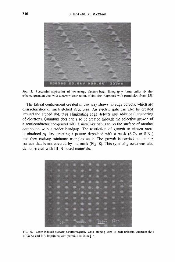
210 S. KIM AND M. RAZEGHI
o f t ; , : : ; J ^ ^ S i ••*••':•
ill*?"
8 5 8 8 t ' S . a k V X 9 « . e n ' ^ ' 3 a ' j n i
FIG. 5. Successful application of low-energy electron-beam lithography forms uniformly dis-tributed quantum dots with a narrow distribution of dot size. Reprinted with permission from [15].
The lateral confinement created in this way shows no edge defects, which are characteristics of such etched structures. An electric gate can also be created around the etched dot, thus eliminating edge defects and additional squeezing of electrons. Quantum dots can also be created through the selective growth of a semiconductor compound with a narrower bandgap on the surface of another compound with a wider bandgap. The restriction of growth to chosen areas is obtained by first creating a pattern deposited with a mask (Si02 or SiN^) and then etching miniature triangles on it. The growth is carried out on the surface that is not covered by the mask (Fig. 8). This type of growth was also demonstrated with III-N based materials.
FIG. 6. Laser-induced surface electromagnetic wave etching used to etch uniform quantum dots of GaAs and InP. Reprinted with permission from [16].
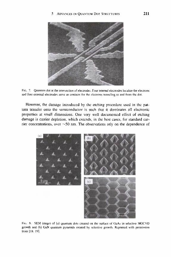
5 ADVANCES IN QUANTUM D O T STRUCTURES 211
FIG. 7. Quantum dot at the intersection of electrodes. Four internal electrodes localize the electrons and four external electrodes serve as contacts for the electrons tunneling to and from the dot.
However, the damage introduced by the etching procedure used in the pat-tern transfer onto the semiconductor is such that it dominates all electronic properties at small dimensions. One very well documented effect of etching damage is carrier depletion, which extends, in the best cases, for standard car-rier concentrations, over ^50 nm. The observations rely on the dependence of
X r
FIG. 8. SEM images of (a) quantum dots created on the surface of GaAs in selective MOCVD growth and (b) GaN quantum pyramids created by selective growth. Reprinted with permission from [18, 19].

212 S. KIM AND M. RAZEGHI
FIG. 9. Evolution of self-assembled quantum dots grown by MBE. Reprinted with permission from [6].
the electronic population of quantum wires or dots on geometric lateral size: below '^100-nm, quantum wires or dots are empty. Another probe of the dam-age is the decrease in luminescence efficiency due to numerous nonradiative defects. To obtain less damaged structures, softer fabrication techniques have been sought. Direct semiconductor growth on vicinal surfaces, step-induced directional growth using the patterned substrate, or growth of cleaved and etched multiquantum well structures on sidewalls have been tried through a delicate two-step growth technique. In addition to the etching damage, overgrowth on the etched pillar and the acquisition of smaller size present other hard tasks for optical devices. Actually, the performance of quantum dot optoelectronic devices has been inhibited mainly due to these limitations in technologies.
Therefore, the emerging growth technology of self-organization of the epi-taxial semiconductor layer on different lattice constant substrates holds great promise for removing complicated technologies. This method, originally called the Stranski-Krastanow (S-K) growth mode, was discovered in 1939 [2] and rediscovered [6] during the epitaxy of InAs on GaAs, where islands form due to the strain of lattice mismatch between the epilayer and the substrate. These islands are small enough to expect quantum size effects, which we call zero-dimensional quantum structure. Figure 9 shows the evolution of InAs quantum dots on GaAs grown by molecular beam epitaxy (MBE).
References
1. R. C. Ashoori, Nature 379, 413 (1996). 2. I. N. Stranski and L. von Krastanow, Akad. Wiss. Let. Mainz Math. Natur Kl lib 146, 797
(1939). 3. L. Goldstein, F. Glas, J. Marzin, M. Charasse, and G. LeRoux, Appl. Phys. Lett. 41, 1099
(1985). 4. R. Notzel, N. Ledentsov, L. Daweritz, M. Hohenstein, and K. Ploog, Phys. Rev. Lett. 67, 3812
(1991). 5. D. Leonard, M. Krishnamurthy, C. Reaves, S. Denbaars, and R Petroff, Appl. Phys. Lett. 63,
3203 (1993). 6. R Petroff, A. Gossard, R. Logan, and W. Wiegmann, Appl. Phys. Lett. 41, 635 (1982). 7. A. Efros, Sov. Phys. Semicond. 16, 702 (1982).

5 ADVANCES IN QUANTUM DOT STRUCTURES 213
8. M. Grundmann, O. Stier, and D. Bimberg, Phys. Rev. B 52, 11,969 (1995). 9. U. Woggon, Festkitper Problem 35, 175 (1995).
10. J. Scott, S. Field, M. Kastner, H. Smith, and D. Antoniadis, Phys. Rev. Lett. 62, 583 (1989). 11. M. Kastner, S. Field, U. Meirav, J. S. Thomas, D. Antoniadis, and H. Smith, Phys. Rev. Lett.
63, 1894 (1989). 12. A. Palevski, C. P. Umbach, and M. Heiblum, Phys. Rev Lett. 62, 1776 (1989). 13. G. Frazier, "Concurrent Computations." Plenum, New York, (1988). 14. H. Wu and D. Sprung, J. Appl. Phys. 84, 4000 (1998). 15. R. Steffen, Th. Koch, J. Oshinowo, F Faller, and A. Forchel, Appl. Phys. Lett. 68, 223 (1996). 16. M. Ezaki, H. Kumagai, K. Toyoda, and M. Obara, Proc. SPIE 2125, 344 (1994). 17. M. A. Reed, Sci. Am. March (1993).

This Page Intentionally Left Blank
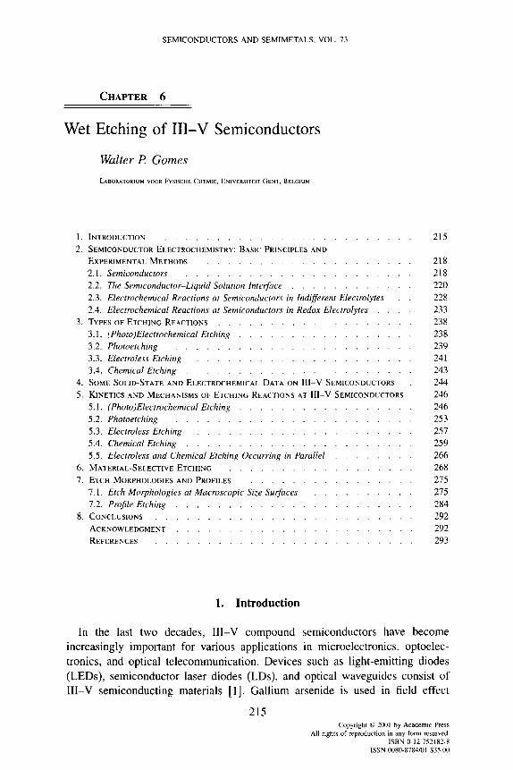
SEMICONDUCTORS AND SEMIMETALS, VOL. 73
CHAPTER 6
Wet Etching of III-V Semiconductors
Walter P. Gomes
LABORATORIUM VOOR FYSISCHE CHEMIE, UNIVERSITEIT GENT, BELGIUM
1. INTRODUCTION 215
2. SEMICONDUCTOR ELECTROCHEMISTRY: BASIC PRINCIPLES AND
EXPERIMENTAL METHODS 218
2.1. Semiconductors 218 2.2. The Semiconductor-Liquid Solution Interface 220 2.3. Electrochemical Reactions at Semiconductors in Indifferent Electrolytes . . 228 2.4. Electrochemical Reactions at Semiconductors in Redox Electrolytes . . . . 233
3. TYPES OF ETCHING REACTIONS 238
3.1. (Photo)Electrochemical Etching 238 3.2. Photoetching 239 3.3. Electroless Etching 241 3.4. Chemical Etching 243
4. SOME SOLID-STATE AND ELECTROCHEMICAL DATA ON I I I - V SEMICONDUCTORS . 244
5. KINETICS AND MECHANISMS OF ETCHING REACTIONS AT III-V SEMICONDUCTORS 246
5.1. (PhotojElectrochemical Etching 246 5.2. Photoetching 253 5.3. Electroless Etching 257 5.4. Chemical Etching 259 5.5. Electroless and Chemical Etching Occurring in Parallel 266
6. MATERIAL-SELECTIVE ETCHING 268
7. ETCH MORPHOLOGIES AND PROFILES 275
7.1. Etch Morphologies at Macroscopic Size Surfaces 275 7.2. Profile Etching 284
8. CONCLUSIONS 292
ACKNOWLEDGMENT 292
REFERENCES 293
1. Introduction
In the last two decades, III-V compound semiconductors have become increasingly important for various applications in microelectronics, optoelec-tronics, and optical telecommunication. Devices such as light-emitting diodes (LEDs), semiconductor laser diodes (LDs), and optical waveguides consist of III-V semiconducting materials [1]. Gallium arsenide is used in field effect
215 Copyright © 2001 by Academic Press
All rights of reproduction in any form reserved. ISBN 0-12-752182-8
ISSN 0080-8784/01 $35.00

216 WALTER P. GOMES
transistors because of the higher mobiUty of electrons in GaAs as compared to silicon, leading to devices that can operate faster [2]. In recent years, semicon-ducting group III nitrides have received great interest because they allow the wavelength range of LEDs and LDs to be extended into the green and the blue, which allows full color displays to be achieved through mixing of the three primary colors [3, 4].
The processing of III-V compound semiconductors for component fabrica-tion involves steps in which material is removed in a controlled way, that is, etching steps. Both dry and wet etching methods are employed. This chapter pertains to wet etching, which is the controlled dissolution of the semiconductor as a consequence of a chemical or an electrochemical reaction. In addition to the controlled dissolution of semiconducting material as such, wet etching also has more specific applications. Whereas the etch morphology often depends on the crystal face, etching is used as a means to identify crystal faces. So-called polishing etchants are used to obtain samples with perfectly smooth surfaces, which is essential in certain process steps [5]. Wet etchants may in many cases react specifically at crystallographic defects such as dislocations, impurity stri-ations, and microprecipitates, and hence have defect-revealing properties [6]. Because the performances of III-V devices are influenced by these defects, etching may hence be used for quality control of semiconducting materials. In many applications, multilayer structures of different III-V semiconductors that are grown epitaxially on a III-V substrate by techniques such as metal-organic chemical vapor deposition (MOCVD) are used. In the processing of these mul-tilayer structures, it is often necessary to remove epitaxial layers selectively with respect to other layers [7]. Wet etchants that exhibit this material selectiv-ity, based upon a difference in reactivity of the etchant with respect to differ-ent semiconductor materials, are available. Finally, in device fabrication, mask etching is often employed. It allows well-defined patterns of etch grooves with predetermined shapes to be obtained. For these process steps, wet etching is also appropriate, because it is known that the shape of the etch grooves is deter-mined not only by crystallographic factors, but also by the etching kinetics and mechanisms.
For many years, etching recipes have been proposed mainly on an empirical basis, that is, as the result of trial-and-error experiments. As a consequence of the increasing variety in materials used (i.e., mixed III-V semiconductors com-posed of more than one group III and/or group V element and with varying composition) and in view of the quite different but very stringent requirements of etching agents for various applications, it has been gradually realized that for an efficient design of etching procedures, a deeper insight is needed into the factors governing the rates of etching reactions and the resulting morphologies, and hence into the mechanisms of etching of semiconductors. Obviously, this objective is not only important from the technological point of view, but also from the scientific. It was further realized that this fundamental approach to the

6 WET ETCHING OF III-V SEMICONDUCTORS 217
etching of semiconductors should be electrochemical. Indeed, wet etching pro-cesses in general take place at a semiconductor-electrolyte interface. Moreover, in certain cases, etching is achieved by integrating the semiconductor as an elec-trode into an electrochemical circuit and by drawing (mostly anodic) current through the semiconductor-electrolyte interface. Even when the etching is per-formed by simply immersing the semiconductor into the electrolyte solution, the net dissolution reaction may be the result of electrochemical steps compensat-ing each other electrically, but not chemically. Gerischer and co-workers [8-11], on the occasion of their electrochemical studies on III-V semiconductors such as GaAs, were probably the first to recognize the potential of semiconductor electrochemistry for investigating the mechanisms of etching processes taking place without any net current flow. In the last 15 years or so, the strategy that consists of combining etch rate measurements with electrochemical studies on the individual steps of etching reactions has been successfully applied to many etching systems, mostly involving III-V semiconductors (for earlier reviews, see, e.g., [12, 13]). The main reasons why III-V semiconductors are especially suited for this line of research is first that most III-V compounds (in contrast to most II-VI compounds) are available both as n-type and p-type semiconduc-tors, allowing identification of the charge-transfer mechanism of electrochemi-cal steps (see further). Second, in contrast to silicon, where one is for a greatly restricted in aqueous media to fluoride or NaOH solutions, at III-V semicon-ductors a large variety of chemicals can be investigated. Later in this chapter we reveal how electrochemical studies may also help to unravel etching mechanisms that are purely chemical; that is, that do not consist of electrochemical partial reactions.
The oudine of this chapter is as follows. Section 2 is devoted to the basic principles and experimental methods of semiconductor electrochemistry. The necessity of such a section is obvious from the foregoing considerations. In Section 3, the four types of etching reactions—(photo)electrochemical etch-ing, photoetching, electroless etching, and chemical etching—are introduced. Section 4 is a short survey of relevant solid-state and electrochemical data on III-V semiconductors. Section 5 contains a detailed discussion on the kinetics and mechanisms of various etching reactions, representative of the previously cited four types of reactions and taking place at different III-V semiconduc-tor materials. In Section 6, the discussion pertaining to the etching kinetics and mechanisms is focussed specifically on the problem of material selectivity, which is important with respect to the etching of multilayer structures as previ-ously mentioned. It is thereby demonstrated that it is essential to know the etch-ing mechanisms to understand and predict material-selective etching. Section 7 pertains to the resulting macroscopic (i.e. at single crystal faces) as well as microscopic (i.e. on the micrometer scale at mask edges) etch morphologies. Both subjects are shown to be closely related; that is, the macroscopic etching kinetics usually constitutes a good guideline for understanding and predicting the shapes of etch profiles near mask edges.
218 WALTER P. GOMES
2. Semiconductor Electrochemistry: Basic Principles and Experimental Methods
In this section, the basic principles of semiconductor electrochemistry are briefly recalled. The discussion mainly is restricted to those aspects that are relevant to the wet etching of semiconductors. We refer to the literature [14-17] for more detailed treatments of this subject.
2.1. SEMICONDUCTORS
The electronic energy levels in semiconductors are grouped into energy bands. The highest (nearly) occupied band is denoted as the valence band and is sep-arated from the lowest (nearly) unoccupied band, the conduction band, by a forbidden region of energy called the bandgap. The width of the bandgap E^ is thus given by
E, = E,-E, (1)
where E^ is the energy at the bottom of the conduction band and E^ is the energy at the top of the valence band. Common values for the bandgap of semi-conductors are between 1 and 3 eV. This range of values implies that under equilibrium conditions at room temperature, only a minor fraction of the valence band electrons will be able to get thermally excited from the valence band to the conduction band and hence to create positive holes h^ (empty levels in the valence band) and conduction band electrons e~ (occupied levels in the conduc-tion band). Because these valence band holes and conduction band electrons are mobile and therefore responsible for the electrical conductivity of the solid, the band structure of most semiconductors is such that they normally are expected to behave as insulators. However, impurities or imperfections in the solid often give rise to localized energy levels in the bandgap. Two types of levels are important with respect to semiconductivity. The first type is that of a donor level; that is, a level close to the conduction band edge E^ and filled with an electron at 0 K. The majority of such levels will have donated their electron to the conduction band at room temperature. If the crystal contains a typical donor density A , of 10 ^ cm~^ and the donor level is close enough to E^, the density of conduction band electrons n will hence be approximately 10 ^ cm~^ at room temperature, giving rise to so-called n-type semiconductivity. The sec-ond type of localized level is that of an acceptor level; that is, a level not far above the valence band edge E^ and being empty at 0 K. At room temperature, most acceptor levels will have extracted an electron from the valence band and thus created a density of holes p, approximately equal to the acceptor density A . A material in which the conductivity is due to holes is denoted as a p-type semiconductor. In certain cases, a solid material will be either an n- or a p-type

6 WET ETCHING OF III-V SEMICONDUCTORS 219
semiconductor because it unintentionally contains a certain density of donors or acceptors, respectively, due to the circumstances under which the crystal was grown. Mostly, however, the material is made semiconducting by intentionally doping it with impurities. For example, gallium arsenide can be made an n-type semiconductor by doping with silicon and p-type by doping with zinc. Note that it is not always possible to achieve a given type of semiconductivity by doping.
The distribution of electrons among the available energy levels of a solid at thermodynamic equilibrium is described by Fermi statistics and characterized by a parameter, the Fermi energy or Fermi level Ep. An electronic level at the Fermi energy has a probability of 0.5 of being filled. The chemical significance of Ep is the electrochemical potential of the electrons divided by the Avogadro constant (i.e., expressed per particle). Usually, the Fermi level is within the bandgap and sufficiently distant (> 2kT) from the band edges. In that case, the Fermi distribution can be approximated by the following Boltzmann-type expressions for the densities of conduction band electrons and of holes:
n = N,cx^[-{E,-E,)/kT] (2)
or
Ep = E^ + kT\n{n/N,) (3)
and
p = N,tx^[{E,-Ep)/kT] (4)
or
Ep = E^,-kT\n{plN,) (5)
N^ and A^ represent the effective density of states at the bottom of the conduc-tion band and at the top of the valence band, respectively. From Eqs. (1), (2), and (4), it follows that
np = N^N^Qxp{-EJkT) (6)
Equation (6) implies that at equilibrium, when n is relatively high (n-type semi-conductor), p will be negligibly small and vice versa. However, nonequilibrium conditions also must be considered. For example, when illuminating the semi-conductor with photons that have an energy hv greater than E^, electrons will be excited from the valence band to the conduction band, leading to an excess of both electrons and holes but affecting, on a relative scale, primarily the den-sity of minority carriers (holes in an n-type and electrons in a p-type semicon-ductor). Under constant illumination, a steady-state density of minority carriers
220 WALTER P. GOMES
will build up, depending on the generation and recombination rates of electrons and holes.
2.2. THE SEMICONDUCTOR-LIQUID SOLUTION INTERFACE
Wet etching of semiconductors implies reactions that occur at a semiconductor-liquid solution interface. In most cases, an (aqueous) electrolyte solution is involved. Therefore, we will first deal with the properties of the semiconductor-electrolyte interface, and more specifically with the charge and potential distribution at this interface.
2.2.7. Charge and Potential Distribution
Consider an electrochemical cell containing a semiconductor electrode SC, and a large area counterelectrode consisting of a metal ME (e.g., Pt) and a ref-erence electrode RF. For the sake of simplicity, assume that all three electrodes are connected to wires consisting of the metal ME. The potential difference (p(hghi)—(p(\efi) in the circuit
ME/RF/EL/SC/ME
is called the electrode potential V of the semiconductor. It is the sum of the potential differences at the individual interfaces of the circuit. In what follows, the potential differences across ME/RF/EL are considered to be constant. Also the contact potential SC/ME can be considered to be constant for a given com-bination of materials. The potential difference of interest here is <Psc/ei' defined as the potential in the bulk of the semiconductor minus that in the bulk of the electrolyte, and hence related to V by
or, under varying V, by
y = <Psc/el+Ct (7)
dV = dcp,,/,, (8)
An accumulation of charges at both sides of the SC/EL interface corresponds to a given <Psc/ei- ^ ^hat follows, assume that the electrolyte solution is concen-trated (c > 0.1 mol r^) . In that case, the charge at the electrolyte side of the interface can be considered to be concentrated in the (outer) Helmholtz plane, that is, the plane of closest approach of solvated ions to the semiconductor sur-face, which is located at about 0.3 nm from the surface. The layer between the surface and Helmholtz plane is called the Helmholtz layer H. It contains pri-marily solvent molecules which are more or less oriented in the electric field at
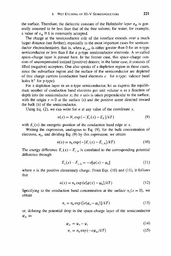
6 WET ETCHING OF III-V SEMICONDUCTORS 221
the surface. Therefore, the dielectric constant of the Helmholtz layer e^ is gen-erally assumed to be less than that of the free solvent; for water, for example, a value of e^ — 6 is commonly accepted.
The charge at the semiconductor side of the interface extends over a much larger distance (see further), especially in the most important cases for semicon-ductor electrochemistry, that is, when (p^^/^^ is either greater than 0 for an n-type semiconductor or less than 0 for a p-type semiconductor electrode. A so-called space-charge layer is present here. In the former case, this space-charge con-sists of uncompensated ionized (positive) donors; in the latter case, it consists of filled (negative) acceptors. One also speaks of a depletion region in these cases, since the subsurface region and the surface of the semiconductor are depleted of free charge carriers (conduction band electrons e~ for n-type; valence band holes h+ for p-type).
For a depletion layer in an n-type semiconductor, let us express the equiUb-rium number of conduction band electrons per unit volume « as a function of depth into the semiconductor x; the x axis is taken perpendicular to the surface, with the origin x = 0 at the surface (s) and the positive sense directed toward the bulk (b) of the semiconductor.
Using Eq. (2), we can write for n at any value of the coordinate x,
n{x) = N,tx^{-[E,{x)-EA/m (9)
with E^{x) the energetic position of the conduction band edge at x. Writing the expression, analogous to Eq. (9), for the bulk concentration of
electrons, n^, and dividing Eq. (9) by this expression, we obtain
n{x) = n,exp {-[E,{x) - E,^,]/kT) (10)
The energy difference E^{x) — E^^ is correlated to the corresponding potential difference through
£ , (x ) -£ , . b = -4<PW- 'Pb] (11)
where e is the positive elementary charge. From Eqs. (10) and (11), it follows that
n{x) = n^ exp {e[cp{x) - (p^]/kT) (12)
Specifying to the conduction band concentration at the surface n^{x = 0), we obtain
n, = /Zb exp i{e{(p, - (p^,)]/kT) (13)
or, defining the potential drop in the space-charge layer of the semiconductor
< sc = <Pb-^s (14)
n^ = n^ exp {-ecp^JkT) (15)

222 WALTER P. GOMES
The analogous expression for the equiUbrium concentration of holes at the sur-face of a p-type semiconductor, p^, is
p, = p^Qxp{e(p,JkT) (16)
Whereas the separation of charges at the interface SC/EL involves two regions, that is, the space-charge layer within the semiconductor and the Helmholtz layer, we can write
^sc/el = i<Ph - <Ps) + ( ^ s - ^d)
= 'Psc + 'Pu (17)
Here, (p^^ represents the potential in the bulk of the electrolyte and cp^ represents the potential drop across the Helmholtz layer. From Eqs. (8) and (17), it follows that, when one changes the semiconductor electrode potential V, for example, by an external voltage supply connected between the semiconductor and the counterelectrode, one changes, in principle, (p^^ as well as (p^. Subsequently, we will see that in many cases the change in (p^ is negligible. Anyway, according to Eqs. (15) and (16), this allows the concentrations of free charge carriers at the surface to change. This point is important as far as semiconductor electrode kinetics is concerned.
The change of the potential (p(x) with distance into the semiconductor elec-trode corresponds to a change in the position of the energy bands. The relation-ship is given by an expression of the type of Eq. (11); that is, the energy bands are bent in the space-charge layer. Figure 1 shows schematically the charge and potential distribution as well as the band-bending in the case of an n-type semi-conductor electrode that is positively charged with respect to the electrolyte. In Figure Ic, the Fermi level is drawn horizontally, because it is assumed that no current flows and hence the system is at equilibrium.
Let us now describe the potential distribution over the interface SC/EL more quantitatively. We again consider the case of an n-type semiconductor polarized positively, that is, ^ c/ei > 0. The starting point of the derivation is the one-dimensional form of the Poisson equation
d^(p{x)/dx^ = -p{x)/soS (18)
where p{x) is the charge density at the position x. Integration of Eq. (18) from X = 0 to jc -> 00 leads to an expression for the total charge per unit of surface area in the space-charge layer Q^^,
Gsc = s,e[dcp{x)/dxl^o (19)
in which s represents the dielectric constant of the semiconductor (note that [dcp(x)/dxU^ = 0).
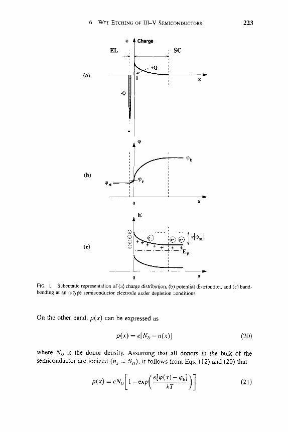
6 WET ETCHING OF III-V SEMICONDUCTORS 223
(a)
(b)
+ i Charge
EL
b<:: +Q
SC
(c) e ©©
+ +
FIG. 1. Schematic representation of (a) charge distribution, (b) potential distribution, and (c) band-bending at an n-type semiconductor electrode under depletion conditions.
On the other hand, p{x) can be expressed as
p(x) = e[Ni) - n{x)] (20)
where A^ is the donor density. Assuming that all donors in the bulk of the semiconductor are ionized {n^ = N^), it follows from Eqs. (12) and (20) that
p{x) = eNJ 1 — exp /e[cp(x) - cp^,]V
V kT ) _ (21)

224 WALTER P. GOMES
Combining Eqs. (18) and (21) yields
.^[l_exp(f[^(^)] (22)
Now consider the mathematical expressions
dx \ dx ) dx^ dx
and hence
dx) J dx^ d(p
Application on Eq. (22) yields
\dx) 2eNn
£nS ^ ( . ) - - e x p ( ^^ + ct
(23)
(24)
(25)
The value of the integration constant follows from the condition (dcp/dx) = 0 for (f = <p^:
2eNr,{ kT\
SQB \ e )
Hence
\dx J SQ£ [ b - <P W ] -
kT 1 — exp
e[(p{x) - <Pb] kT
Specifying to jc = 0 and in view of Eq. (14),
dcpV 2eNa\ kT\ ( eip,,V\\
(26)
(27)
(28)
In the so-called Mott-Schottky approximation, it is assumed that e(p^^ ^ kT, so that the exponential term can be neglected, and Eq. (28) reduces to
kT
e
1/2
(29) \dx)^^Q \ e^e ) \ '
Combination of Eqs. (19) and (29) yields
6.0 = {2e,eeN^y'\<p^ - kT/eY" (30)
The countercharge of the space-charge is located in the Helmholtz plane:
\QH\ = QSC (31)

6 WET ETCHING OF III-V SEMICONDUCTORS 225
According to Eq. (18), because no charges are present within the Helmholtz layer, the potential drop over this layer is linear,
dip/dx = ct = (Pu/d^i (32)
where d^ is the width of the Helmholtz layer (= 3 x 10"^^ m). Application of Eq. (19) to the Helmholtz layer yields
\QH\ = ^ 0 % ^ H / ^ H = 2sc (33)
From Eqs. (30) and (33), it finally follows that
^^ = (2s,seN,y^^-^L-^-^Y (34)
The discussion of the relative contributions of (p^^ and ( H to ( sc/ei [s^^ Eq. (17)] is somewhat hampered by the fact that the relationship (34) is not linear. As an example, consider typical values of (p^^ == 0.2 V, A , = 10 ^ cm~^ = 10 ^ m~^ and e = 5. Equation (34) then yields a value of (p^^ = S.S x 10'"^ V = I mV, which is negligible with respect to cp^^. In most cases, (p c/ei can hence be approximated by (Psc and Eq. (7) can be approximated by
^ = ^sc/el + ^^ = 9sc + ^^ (35)
The fact that the potential drop ( c/ei occurs practically exclusively over the space-charge region of the semiconductor is due to the relatively low concen-tration of charge carriers w = A ^ in the semiconductor. This can easily be seen by repeating the preceding calculation for a typical metal such as silver, with n^^ = 6x 10 ^ m~ . Here, the potential drop is found to be predominantly over the Helmholtz layer.
Note that in many cases the Helmholtz potential contains a potential-dependent contribution that has not been considered in the foregoing derivation, because surface charges are involved that are not due to the application of a potential difference < sc/ei' t>ut to the establishment of an acid-base or an adsorp-tion equilibrium at the surface (see further). This V-independent contribution is hence included in the constant term of Eq. (35). It should be kept in mind that this contribution can vary with the composition of the electrolyte (e.g., with pH).
In addition to depletion, other situations may occur at a semiconductor elec-trode surface, depending on bias. In Figure 2, depletion, flat-band situation, and accumulation are depicted for an n- as well as for a p-type electrode. One more possible situation is not shown in the figure, that is, inversion. By inversion we mean the following. In the case of an n-type electrode, for example, when the positive bias is so large that the Fermi level at the surface is below the middle of the bandgap, the equilibrium surface concentration of holes should exceed that of electrons; that is, holes should be created at the surface. When the band-bending is not too large, this inversion phenomenon is usually not observed with wide-bandgap semiconductors.

226 WALTER P. GOMES
n
P
L
Depletion
I
c
^
EL
1
:
VB
sc
E
i
K
Y^ ©©©©
Flat-band
E
I
'(JJ<5X'X«-3C«X«-XO + + + + + + +
E
b©©©©©©
Accumulation
1 j
I
5
1 ^ + + + + + + 1
r
I
1
^
<i (W©©00©©©
FIG. 2. Depletion, flat-band, and accumulation at n- and p-type semiconductor electrodes.
Note that when changes in the applied bias may be assumed to have no effect on the Helmholtz potential drop, the potential at the electrode surface, cp^, can be considered to be fixed with respect to a reference level in the electrolyte or to the potential of the reference electrode, meaning that the band edges remain fixed with respect to the corresponding reference level. Hence the bands in the bulk of the semiconductor move up or down when the electrode potential is varied. As will become clear in the following sections, knowledge of the energetic position of the band edges at the surface E^ ^ and E^ ^ is of crucial importance to understanding the reactivity at the semiconductor-liquid interface. This position can be determined from knowledge of the flat-band potential V^^, that is, the potential of the semiconductor electrode with respect to the reference electrode corresponding to the flat-band situation. Whereas in that case (p^^ = 0, Vfb corresponds to the constant term in Eq. (35), so that
y-y^^'p. (36)
The flat-band potential measures the Fermi level of the semiconductor at the flat band with respect to that in the reference electrode:
E'F,f^^-eV^ (37)
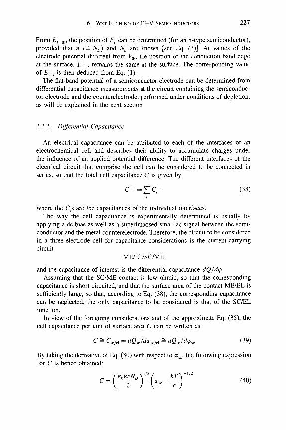
6 WET ETCHING OF III-V SEMICONDUCTORS 227
From Epj^, the position of E^ can be determined (for an n-type semiconductor), provided that n (= A ,) and A^ are known [see Eq. (3)]. At values of the electrode potential different from V^, the position of the conduction band edge at the surface, E^^^, remains the same at the surface. The corresponding value of £'y s is then deduced from Eq. (1).
The flat-band potential of a semiconductor electrode can be determined from differential capacitance measurements at the circuit containing the semiconduc-tor electrode and the counterelectrode, performed under conditions of depletion, as will be explained in the next section.
2.2.2. Differential Capacitance
An electrical capacitance can be attributed to each of the interfaces of an electrochemical cell and describes their ability to accumulate charges under the influence of an applied potential difference. The different interfaces of the electrical circuit that comprise the cell can be considered to be connected in series, so that the total cell capacitance C is given by
C-'=J:C-' (38)
where the Qs are the capacitances of the individual interfaces. The way the cell capacitance is experimentally determined is usually by
applying a dc bias as well as a superimposed small ac signal between the semi-conductor and the metal counterelectrode. Therefore, the circuit to be considered in a three-electrode cell for capacitance considerations is the current-carrying circuit
ME/EL/SC/ME
and the capacitance of interest is the differential capacitance dQ/dcp. Assuming that the SC/ME contact is low ohmic, so that the corresponding
capacitance is short-circuited, and that the surface area of the contact ME/EL is sufficiently large, so that, according to Eq. (38), the corresponding capacitance can be neglected, the only capacitance to be considered is that of the SC/EL junction.
In view of the foregoing considerations and of the approximate Eq. (35), the cell capacitance per unit of surface area C can be written as
C S Q / e l = ^Csc/^^sc/el - dQJd<p^ (39)
By taking the derivative of Eq. (30) with respect to cp^^, the following expression for C is hence obtained:
C = ( £ ^ ) ' " ( , . - ^ ) - " ' (40,

228 WALTER P. GOMES
or
C^ SoSeNj) \ e )
Inserting Eq. (36) into Eq. (41), the so-called Mott-Schottky relationship is obtained:
\-^{v-V^-'^\ (42)
This equation predicts a linear relationship between C~^ and the electrode poten-tial V, which, in principle, allows the following data that are essential to the study of electrode kinetics, to be obtained:
1. The point of extrapolation of the Mott-Schottky plot with the V-axis leads to the determination of V ,-
2. The slope of the Mott-Schottky plot yields the donor density A , pro-vided that e and the surface area of the electrode are known (remember that C is the capacitance per unit area).
3. The knowledge of V^ allows determination of (p^^ at given V [see Eq. (36)] and hence n^ [see Eq. (15)].
4. Still under the assumption that the variation of ( ^ with W is negligible, the (fixed) position of the band edges at the surface E^ ^ and E^^ can be determined; see Section 2.2.1.
Considerations that are analogous to the preceding can be held for a p-type semiconductor electrode. The form of the Mott-Schottky relationship in this case is
1
C^ e^eeNj^ ( - V + V , - ^ ) (43)
Experimentally, it is often found that C at fixed electrode potential V depends on the frequency / of the ac signal used, indicating that the foregoing assump-tions made for an ideal Schottky barrier and on which this simple derivation was based are not always fulfilled. Whereas usually Mott-Schottky plots recorded at different measuring frequencies more or less converge to a common point on the potential axis, the flat-band potential can still be approximately determined in such cases. For a recent discussion on this problem, see [18].
2.3. ELECTROCHEMICAL REACTIONS AT SEMICONDUCTORS IN
INDIFFERENT ELECTROLYTES
We now briefly discuss the current-potential behavior of semiconductor elec-trodes immersed in an indifferent electrolyte solution, that is, in a solvent

6 WET ETCHING OF III-V SEMICONDUCTORS 229
containing ions that do not react electrochemically. The discussion is restricted to aqueous medium.
Figure 3a shows typical current density (j) vs. potential (V) curves for an n-type semiconductor in darkness (curve 1) and under illumination with photons having an energy hv > E^ (curve 2). Curve 1 demonstrates the rectifying char-acteristics of a semiconductor-electrolyte contact: in the anodic sense, a low nearly constant current is observed {j typically between 1 nA cm~^ and 1 /JLA cm"^), whereas in the cathodic sense, the current rises exponentially when the potential becomes more negative. Whereas the latter sense is that in which the electron concentration at the surface increases exponentially [Eq. (15)], the elec-trochemical reaction involved obviously requires the participation of conduction
"a,
1 / ^
(1,2)
n-type
/ / / / / /
/ f
(a)
(2)
(1)
V
FIG. 3. Schematic current density vs. potential curves, (a) n-type electrode; (b) p-type electrode; 1, darkness, 2, light.

230 WALTER P. GOMES
band electrons (electron capture). [Note that usually this exponential current range is found under depletion (V > Vf^^), due to the relatively high electron cap-ture rate constant.] The corresponding reaction appears to be the reduction of water molecules or of protons, resulting in hydrogen evolution. In certain cases, a small fraction of the cathodic current is associated with the reduction of the semiconductor material itself; for example, in the case of InP, the formation of some metallic In is observed.
Curve 2 shows that the anodic current is gready enhanced by illumination. The difference between the current under illumination and that in darkness is denoted as the photocurrent. The onset of the photocurrent curve is in a poten-tial range that is positive to the flat-band potential. Considering the sense in which the energy bands are bent under these circumstances, the occurrence of a photocurrent can be interpreted as follows (Fig. 4a). The electrons and holes, which are formed by absorption of photons, are separated by the electric field in the depletion layer. The holes move to the surface, where they undergo elec-trochemical reactions, and the electrons are drawn into the bulk and from there into the external circuit (at V < Vf , the holes formed by light immediately recombine with electrons due to the large density of majority carriers at and near the surface). Because the photoinduced charge carriers have a finite life-time before recombining, holes created in a region behind the depletion layer, denoted as the diffusion layer, also may reach the depletion layer and hence the surface. In most cases, the reaction associated with the photocurrent is found to be the anodic oxidation of the semiconductor material; in some cases, in aque-ous media, the oxidation of the solvent to O2 is involved (Ti02, SrTi03). In view of the scope of this chapter, we restrict the discussion to the anodic oxi-dation of the semiconductor. Apparently, because this reaction does not occur in darkness at n-type electrodes, at least the first step of this multiequivalent
n-type p-type
EL EL
hu
(a) (b) FIG. 4. Mechanism of photocurrent generation at n- and p-type semiconductor electrodes.
6 WET ETCHING OF III-V SEMICONDUCTORS 231
oxidation reaction requires a valence band hole. Since the valence band is com-posed of the bonding states of the semiconductor, holes at the surface corre-spond to electrons being removed from surface bonds. The problem of whether or not the subsequent steps are so-called hole-capture steps will be addressed subsequently. The photocurrent curve exhibits an onset region (normally rather close to the flat-band potential), the shape of which is mainly determined by sur-face charge-carrier recombination, followed, at not too high light intensities, by a saturation region in which the current density is governed by the rate at which the holes are created by light and, therefore, it is proportional to the light inten-sity. At higher light intensities, various types of alternative behavior may occur. When the dissolution rate of the oxidation products is relatively low, the pho-tocurrent may go through a maximum with increasing potential and then drop to a lower level, where this typical passivating behavior is due to the forma-tion of a product layer on the surface. Under certain circumstances, the anodic oxidation reaction may require the participation of ions from solution for the formation of soluble products (e.g., 0H~ ions to form oxyanions); in that case, at high light intensities, diffusion of these ions toward the electrode surface may become rate-determining (see subsequent text).
Figure 3b shows typical j \s. V curves for a p-type semiconductor in dark-ness (curve 1) and under illumination (curve 2). The cathodic current density is low in darkness, but enhanced by light. Whereas under the given circumstances, photogenerated conduction band electrons are drawn toward the electrode sur-face (see Fig. 4b), it can again be concluded that the hydrogen evolution reaction is a conduction band process. In the anodic sense, the current rises exponen-tially. This can easily be understood by keeping in mind that the first step of the anodic dissolution reaction occurs by hole capture. If the various steps of this multiequivalent reaction are irreversible, the steady-state current density can be written as
j = nFkp.c, (44)
where n is the equivalence of the reaction, F is the Faraday constant, k is the rate constant of the first step, and c^ is the surface concentration of the reactant needed to form the soluble oxidation products. The exponential rise of j is then attributable to that of p^ with cp^^ [Eq. (16)] and hence with V [Eq. (36)]. From these equations, a rise of j by a factor of 10 per 60 mV potential increase is expected. In most cases, for reasons that are not clearly established, the curve is less steep than expected. Also here, passivation effects may occur at higher current densities, due to layer formation.
It should be stressed that in case the anodic oxidation products are soluble, the (photo)anodic reaction under consideration amounts to the electrochemical etching of the semiconductor.
The equivalence n of the anodic dissolution reaction can be determined, based on Faraday's law, from the total amount of (photo)anodic charge drawn over a

232 WALTER P. GOMES
certain amount of time and the corresponding amount of semiconductor material dissolved. The latter quantity can be determined after the passage of current, either by analyzing the cell solution or by measuring the etch depth (using a mask to cover part of the surface from the solution to make the difference between the etched and the unetched surface visible). The value of n for a given reaction in a given medium, combined with chemical considerations, then leads to information on the oxidation products.
The question arises whether or not the subsequent steps of the (photo)anodic oxidation reaction of semiconductors are hole-capture steps. Indeed, let us rep-resent the capture of a hole in a surface bond of a semiconductor AB by the reaction equation
A : B + h + - > A « B (45)
The surface species A • B is then an oxidation intermediate that has an unpaired electron that is no longer in a valence band level, but in a surface state, that is, an energy level in the bandgap at the surface [19]. Therefore, A#B may, in principle, be further oxidized either by capture of a second hole,
A • B + h+ -^ products (46)
or by injection of an electron into the conduction band,
A • B -^ e~ + products (47)
[We do not specify here the nature of the surface products formed in reac-tions (46) and (47). In most cases, several electrochemical steps are needed before soluble products are formed.] Electron injection [reaction (47)] is expected to occur only if the corresponding surface state is sufficiently close to the conduction band edge, which in many cases seems to be rather improbable [19].
Several methods may be used to investigate the contribution of electron injec-tion to (photo)anodic dissolution. An appropriate technique for the photoanodic dissolution of n-type semiconductors is intensity-modulated photocurrent spec-troscopy (IMPS). At a constant potential in the photocurrent saturation region, a harmonically modulated light source is superimposed upon the base illumina-tion, creating a modulated hole flux toward the n-type semiconductor surface. It has been shown that, due to the extremely fast separation of photogenerated electron-hole pairs, the harmonically varying concentration of holes at the sur-face is always in phase with the light source. In the absence of reaction step (47), the current in the external circuit also is in phase with the light intensity. If, however, the second step of the photoanodic dissolution reaction is reaction (47) (for simplicity, we assume here that the overall reaction is two-equivalent), the fact has to be taken into account that such an electron injection step is char-acterized by a time constant, so that the current may lag behind with respect to the modulated light intensity over a certain phase angle. Only at very low

6 WET ETCHING OF III-V SEMICONDUCTORS 233
frequencies of the modulated light is the modulated injection current density in phase with the light source. In contrast, at very high frequencies, the hole cur-rent [reaction (46)] is measured exclusively. Hence by measuring the photore-sponse as a function of frequency, the contribution of electron injection steps to photoanodic dissolution can be detected. More quantitative considerations on this method can be found in the literature [20, 21] and in further sections of this chapter.
In addition to IMPS, electron injection during anodic dissolution of semi-conductors may be investigated by other methods, which are summarized, for example, in [13], some of which are discussed further in this text.
2.4. ELECTROCHEMICAL REACTIONS AT SEMICONDUCTORS IN
REDOX ELECTROLYTES
From the electronic point of view, an oxidizing agent in solution, ox\ can be considered as an empty energy level, and the corresponding reducing agent red^~^ can be considered as a filled energy level (for simplicity in what fol-lows, one-equivalent redox couples are considered). Cathodic reduction of an oxidizing agent at a semiconductor electrode then amounts to electron transfer from a semiconductor level to an empty level in solution; anodic oxidation of a reducing agent amounts to electron transfer from a filled level in solution to an empty level in the semiconductor. The generally accepted theory for these processes was developed by Gerischer [14, 15]. The basic idea is that elec-tron transfer occurs by tunneling through the Helmholtz layer, and thus occurs between electron levels at equal energetic height. To understand electrochemi-cal reactivity, the energy level distribution of the redox couple in solution with respect to that in the semiconductor must be known. Due to the difference in solvation structure between the oxidizing agent and the corresponding reduc-ing agent, the energy of the most stable empty and filled redox states, E" and E^^, respectively, differs considerably. More specifically, it can be shown that the empty level is higher in energy than the filled level over an amount 2A ,
E:,-E:,^2K (48)
in which A , the rearrangement energy, is related to the rearrangement taking place in the solvation structure of the ion when this ion either takes up or gives off an electron. Reliable data on A are not currendy available; values reported in the literature often are between 0.4 and 1.2 eV, depending on the redox couple considered.
Owing to fluctuations of the solvation shell of the ions, the redox energy states do not constitute discrete levels, but are distributed over a certain energy range. In Gerischer's theory, the densities of energy functions are described by

234 WALTER P. GOMES
Gaussian functions, D^^ and Dj. , the widths of which are again determined by the rearrangement energy of the redox couple
D„,~exp[-(£-£-) V4A,A:r] (49)
and
£>red~exp[-(£-£- , ) V4A,^r] (50)
(see Fig. 5). It can be shown that the Fermi level of the redox couple at equal activities of the oxidizing and the reducing agent, ^^ redox' i energetically mid-way between the maxima of the empty and filled level curves:
^F, redox =EI,+K=E:, (51)
Whereas £ ^ redox [measured with respect to the Fermi level in the standard hydrogen electrode (SHE)] is related to the standard redox potential of the couple U° by
£;,redox = - ^ t / ° (52)
the U° value can be used as a rough measure for the energetic position of the redox levels. When also expressing the position of the semiconductor band edges at the surface E^^ and E^^^ with respect to the SHE, mutual compari-son between energy level positions at both sides of the semiconductor-redox electrolyte interface becomes possible, which is essential for discussing electro-chemical reactivity.
D(E)
FIG. 5. Gaussian curves that represent the energetic distribution of redox levels in solution.

6 WET ETCHING OF III-V SEMICONDUCTORS 235
Since in principle, electrons for cathodic charge transfer may originate either from the conduction band or from the valence band of the semiconductor elec-trode, two types of cathodic reactions are possible:
o x ^ - h e - - ^ r e d ' - ^ (53)
and
o x ^ - ^ ^ r e d ^ - ^ + h + (54)
The first type is the capture of a conduction band electron, a process that was discussed previously (Section 2.3). Reaction (54) describes the uptake by the oxidizing agent of an electron from the valence band of the semiconductor, leading to the creation of a hole in that band; therefore this process is denoted as hole injection.
Similarly, two types of anodic oxidation reactions may occur, depending on whether the conduction or the valence band is involved, that is, electron injection and hole capture [reactions (55) and (56), respectively]:
r e d ^ - ^ - ^ o x ^ + e- (55)
r e d ' - * + h + - ^ o x ^ (56)
Whether or not cathodic or anodic current flow can occur depends on the relative positions of the Fermi levels in the semiconductor and in the redox electrolyte. If a reaction is thermodynamically possible and if the surface reaction is rate-determining, the current densities corresponding to reactions (53)-(56) can be expressed by the following respective equations, taking into account the sign conventions for electrochemical currents:
(57)
(58)
(59)
(60)
(CQX and Cred represent concentrations in the outer Helmholtz plane.) The rate constants in these equations evidently depend on the relative posi-
tions of electron energy levels at both sides of the interface. For example, hole injection requires that the empty redox levels overlap with the valence band of the semiconductor and hence have a relatively low position in the energy dia-gram. Considering Eq. (52), such behavior may be, in general, expected for a (one-equivalent) redox couple that has a high standard redox potential; that is, a relatively strong oxidizing agent.
Jc, c
Jc, V
Ja, c
Ja, V
— ^^c,
= e^c.
= ^^a.
= ^^a.
c^ox^s
c
c^red
u^redA

236 WALTER P. GOMES
It also follows from these equations that the rate of the injection pro-cesses (54) and (55) is expected to be independent of the electrode potential V (as long as the position of the band edges at the surface is independent of V; see subsequent sections). This means, for example, that hole injection, when it occurs cathodically, also is expected to occur anodically. Anodically, however, the consumption of the oxidizing agent cannot be measured as an external cur-rent, but has to be detected by other methods. An appropriate method is rotating ring-disk voltammetry (see, e.g., [22, 23]). In this method, the semiconductor, in the shape of a circular disk, is concentrically surrounded by a thin metal ring. Ring and disk are electrically insulated from each other and are incorpo-rated in separate electrochemical circuits. This electrode setup can be rotated at a controlled speed around an axis, perpendicular to the plane of the ring and the disk and passing through the center of the disk. Due to the rotation, the solu-tion flows from the bulk to the disk and from there to the ring, so that products formed electrochemically at the semiconductor disk may be detected quantita-tively through electrochemical reaction at the ring, that is, by measuring the ring current.
The rates of the electron and hole capture reactions are proportional to the sur-face concentration of electrons and holes, respectively [Eqs. (57) and (60)]. At p-type semiconductors, reaction (53) therefore does not occur in darkness, since virtually no conduction band electrons are available. This reaction becomes pos-sible under bandgap illumination however (cathodic photocurrent). The shape of the photocurrent curve is analogous to that discussed in Section 2.3. At n-type electrodes, the rate of reaction (53) is expected to increase exponentially when V is lowered. [Also here, in many cases k^ ^ is sufficiently large so that the reac-tion may occur under depletion (V > V ,) at considerable rates.] Similarly, hole capture can occur in darkness at p-type electrodes only; at n-type electrodes, illumination is required (anodic photocurrent).
In the case of two-equivalent electrochemical reactions, a particular class of reactions—so-called current-doubling reactions—deserves special attention. The current-doubling effect was first observed at the (n-type) ZnO electrode [24, 25]. At given light intensity, the limiting (anodic) photocurrent was found to be approximately doubled when certain two-equivalent reducing agents were added to the indifferent electrolyte solution. This effect was explained by a mechanism analogous to that described by Eqs. (45) and (47) for the photoanodic oxidation of n-type semiconductors (chronologically, the latter was observed experimen-tally much later). The assumption is that the two-equivalent reducing agent A captures a photogenerated hole from the electrode to form a radical-type inter-mediate A" * that has highly reducing properties so that the corresponding filled redox levels are close to or above the conduction band edge so that in a second step, the intermediate injects an electron into the conduction band to form A^+:
A + h+-> A+* (61)
A+->A2+ + e- (62)

6 WET ETCHING OF III-V SEMICONDUCTORS 237
In this way, for each photogenerated hole reacting at the surface, two electrons flow through the external circuit. If, in an indifferent electrolyte, the photoanodic reaction involves hole capture steps only, the saturation photocurrent is doubled by adding the reactant.
Shortly after photoanodic current-doubling was detected, its cathodic coun-terpart was also reported [26] on p-type GaP with two-equivalent oxidizing agents (B) such as hydrogen peroxide and the persulfate ion. The reduction mechanism can be denoted here as
B + e - ^ B - (63)
B-->B^-H-h+ (64)
where B~* is a strongly oxidizing radical such as OH* with empty redox levels located near or below the valence band edge. In view of the electrochemical approach for studying etching mechanisms, the latter type of current-doubling reaction is especially important in the framework of this chapter on etching of III-V compounds, because current-doubling oxidizing agents are often found to be etchants for III-V compounds.
Two important remarks have to be made at this point. The first one is that complications may arise in semiconductor electrode reactivity due to surface states. As an alternative route to direct charge transfer as described previously, charge transfer may occur in two steps, that is, first from the semiconductor bands to surface states and then from surface states to redox species in solution or vice versa. Furthermore, the filling or emptying of surface states may lead to charge accumulation at the electrode surface and hence to the unpinning of the band edges, with evident consequences on the magnitude of the electrochemical rate constants.
The second remark is that at high current densities, mass transport may become the rate-limiting factor of electrochemical reactions. Indeed, due to the high reaction rate, the surface concentration of the oxidizing or the reduc-ing agent may become considerably less than the bulk concentration, so that the electrochemical reactant has to be transported to the surface by diffusion. This leads to a potential-independent current density j^-^ff that, for rotating elec-trodes in which the transport is by convective diffusion, obeys to the Levich equation [23]
j , ^ = 0.155 nFD'/\p/r]y/'w'/'c (65)
In this equation, y iff is the limiting current density in amperes per centimeter squared, n is the number of charge carriers involved in the reaction, D is the diffusion coefficient (in meters squared per second), and c is the concentration (in moles per liter) of the rate-limiting species, p is the density (in kilograms per cubic meter) and r] is the viscosity (in kilograms per meter per second) of the electrolyte solution, and w is the rotation rate of the electrode (per second).

238 WALTER R GOMES
Hence, a limiting current can be identified as diffusion-limited if, at a rotating (ring-) disk electrode, it is found to be proportional to the square root of the rotation rate of the electrode. We recall that diffusion limitation may also occur in an indifferent electrolyte; for example, in the (photo)anodic dissolution of semiconductors in an alkaline medium, the current density may be limited by diffusion toward the electrode of the 0H~ ions necessary to form soluble anions of the lattice constituents (see Section 2.3).
3. Types of Etching Reactions
3.1. (PHOTO)ELECTROCHEMICAL ETCHING
(Photo)electrochemical etching amounts to the (photo)anodic oxidation of the semiconductor under conditions in which the oxidation products are soluble (see Section 2.3). This type of etching has the practical disadvantage that the semiconductor has to be incorporated into an electrochemical circuit; that is, that electrical contact has to be made to connecting wires. On the other hand, (photo)electrochemical etching also offers certain advantages. The amount of semiconductor removed by etching can be controlled coulometrically, that is, through the total anodic charge drawn, provided that the equivalence of the reac-tion involved is known [cf. Eq. (44)]. Also, as mentioned later in this chapter, well-determined morphologies (e.g., porous surfaces) may be induced by choos-ing the appropriate range of applied potentials. Because holes are needed for the anodic dissolution of semiconductors, this process occurs in darkness with p-type semiconductors, whereas for n-type semiconductors, illumination with photons of the appropriate energies is required; that is, the dissolution is pho-toelectrochemical. Special advantages are in principle inherent to the latter pro-cedure. Indeed, local photoelectrochemical etching of well-defined areas on the semiconductor surface may be achieved either by using a thin light beam or by covering chosen parts of the surface from the light. Also, when multilayer structures consisting of semiconductor materials with different bandgaps are involved, material-selective etching of a semiconductor with a narrower bandgap with respect to one having a wider bandgap may be performed by choosing the wavelength range of the light such that only in the former case are electron-hole pairs produced.
Next to (photo)electrochemical etching, three types of etching reactions can be distinguished that involve no net current flow, which is obviously more attrac-tive from the technological point of view: the semiconductor sample is simply immersed in the etchant solution and, in certain cases, illuminated with light of appropriate wavelengths. These three types of etching are photoetching, electro-less etching, and chemical etching. The first type occurs under illumination; the other two in darkness. The first two involve an electrochemical mechanism; the third one does not. We now briefly introduce the principles and characteristics of these three types of etching reactions.

6 WET ETCHING OF III-V SEMICONDUCTORS 239
3.2. PHOTOETCHING
Consider again photoelectrochemical etching as depicted in Figure 4a, which shows an n-type semiconductor under anodic bias and illuminated by photons with energy larger than the bandgap. The photogenerated holes are assumed to oxidize and hence to etch the semiconductor. The electrons flow through the external circuit and reduce some oxidizing agent at the counterelectrode. In the case of photoetching, there is no external circuit. (It should be noted here that a certain confusion in terminology exists in the literature; therefore it is stressed that by photoelectrochemical etching and by photoetching, we mean etching under illumination with and without external current flow, respectively.) Hence in photoetching, the photogenerated electrons have to be consumed at the semiconductor-electrolyte interface; that is, they react with an oxidizing agent. The levels of the oxidizing agent required for photoetching should hence over-lap with the conduction band of the semiconductor (Fig. 6). The net photoetch-ing process thus proceeds by an electrochemical mechanism that consists of two partial currents (photoanodic dissolution of the semiconductor and cathodic reduction of the oxidizing agent; Fig. 7a) that compensate each other electrically but not chemically.
The corresponding reactions can be written as
/zz^->e"+h+
SC-\-n h" ^- dissolution products
n (ox^ 4-e~ -^ red^~^)
SC-\-n ox^—> dissolution products+ /2 red^~^ (66)
FIG. 6. Mechanism of photoetching.

240 WALTER P. GOMES
n-type SC + iih+ -> diss, prod
i z - l
p-type
SC + 7
1
i
J
1
i
'
ox + e~
nh+ ->
-> red -
diss.
-1
(b)
1
1 1
/I 1
prod —^ // 1 /
/ i / V
•'^ i J /V ''''
/' / \ /''
/ / \
FIG. 7. Schematic representation of partial and total current density curves at an illuminated semiconductor electrode in an electrolyte solution that contains an electron-capturing oxidizing agent, (a) n-type; (b) p-type. Photoetching occurs at V,.
(for simplicity, one formula unit of the semiconductor SC is assumed to be oxidized by n holes, whereas the reduction of the oxidizing agent is assumed to be one-equivalent).
Combination of etch rate and electrochemical measurements in principle allows us to check whether this simple photoetching model holds. Indeed, in this case, the open-circuit etch rate should correlate with the cathodic current den-sity at open-circuit potential under illumination V^ (see Fig. 7a), which can be measured separately (e.g., by working with chopped light). From Figure 7a, it is obvious that the open-circuit photoetch rate is determined by the relative posi-tions of both partial current curves. A high photoetch rate, at given light inten-sity and oxidizing agent concentration, implies a steep onset of the photocurrent

6 WET ETCHING OF III-V SEMICONDUCTORS 241
curve and hence a relatively low surface electron-hole recombination rate and a high electron capture rate constant k^^ [see Eq. (57)].
Figure 6 equally applies to the photoetching mechanism at p-type semicon-ductors. The corresponding partial current density curves are schematically rep-resented in Figure 7b. The comments are analogous to those applying to n-type samples.
The particular advantages of light-assisted etching are essentially the same as those enumerated in the previous section.
3.3. ELECTROLESS ETCHING
Electroless etching occurs in darkness but is otherwise rather analogous to photoetching as far as the mechanism is concerned. Indeed, here also the net etching reaction is the sum of two electrochemical steps that cancel each other electrically but not chemically. The anodic step is the same as in photoanodic etching or in photoetching; that is, hole capture leads to dissolution of the semi-conductor. The cathodic step is the injection of holes by an oxidizing agent. The empty levels of the etching reactant must hence overlap with the valence band of the semiconductor in this case. Under the same assumptions as those accom-panying reaction Eq. (66), the electroless mechanism can be symbolized by
SC H- n h^ ^- dissolution products
n (ox'^red'~^-hh+)
SC + n ox^ -^ dissolution products+ « red^~^ (67)
that is, the holes injected by the oxidizing agent are consumed in the oxida-tion reaction of the semiconductor. This mechanism is illustrated in Figure 8a by a current density vs. potential diagram pertaining to a p-type semiconductor. The diagram is based on the simple assumption that the hole injection current is potential-independent (see Section 2.4). The actual etching conditions corre-spond to the rest potential V , which is a mixed potential, and imply that the anodic dissolution current adjusts itself to the constant cathodic reduction cur-rent. At V >V^, all injected holes are consumed in the etching reaction. At potentials sufficiently negative with respect to V , the injected holes lead to cathodic current flow. In the case of an n-type semiconductor, where the cur-rent is transported by conduction band electrons, the graphical representation of electroless etching requires more attention. Indeed, in that case, the injected holes constitute the minority carriers, so that the situation is similar to that under illumination, where the holes are created by light. Hence, one has to construct a fictitious anodic curve in the current-potential diagram (Fig. 8b) that has a shape analogous to the photocurrent curve. At potentials close to the flat-band

242 WALTER P. GOMES
p-type
1 (
1 SC + nh+ -> diss, prod -^ / li
1
1
(a)
n-type SC + nh+
/
ox + e~ ^ red^
-^ diss, prod
:
' \ V 1
(b) FIG. 8. Schematic representation of partial and total current density curves at a dark semicon-ductor electrode in an electrolyte solution that contains a hole-injecting oxidizing agent, (a) p-type; (b) n-type. Electroless etching occurs at V .
potential the injected holes recombine with electrons, which are here the major-ity charge carriers. At more positive potentials, the injected holes remain at the surface, where they oxidize the semiconductor. We note that, in contrast to the case of photoanodic dissolution, in electroless etching, current flow takes place when the holes recombine with electrons (the current is transported through the n-type sample by conduction band electrons), whereas no net current flows when the holes do not recombine. The fictitious anodic current-potential curve in Figure 8b reaches a limiting value that is equal to the absolute value of the Hmiting cathodic hole injection current (it is again assumed that the hole injec-tion rate is potential-independent). The resulting current-potential curve does not

6 WET ETCHING OF III-V SEMICONDUCTORS 243
tend to zero at positive potentials due to the contribution of electron injection to the anodic dissolution reaction (see Sections 2.3 and 5.1) that causes a small net anodic current. As a result, also with n-type semiconductors, a rest poten-tial V is defined (see Fig. 8b), at which the actual electroless etching occurs. It can be seen from Figure 8b that the etch rate at V corresponds to the limit-ing current density of the fictitious anodic dissolution curve. This point will be important in the discussion of the etch morphologies (see Section 7).
It is obvious for electroless etching also that combining etch rate and elec-trochemical measurements may lead to detailed insight into the reaction mech-anism. This will be illustrated by selected examples further on in this chapter.
3.4. CHEMICAL ETCHING
In a chemical etching mechanism, no free charge carriers from the semi-conductor (i.e., neither conduction band electrons nor valence band holes) are involved. The etching reaction amounts to the breaking of surface bonds of the semiconductor by the etchant and the formation of new bonds between the semi-conductor constituents and species from solution. For example, the first step of the etching of InP by HCl can be represented by
CI — H CI H
- I n - P - ^ - l L p - ( ) / \ / \
As this example shows, etchants operating by a chemical mechanism are not necessarily oxidizing agents, although they mostly are. For instance, oxidizing agents such as H2O2 and dihalogens act as chemical etchants.
Although chemical etching reactions are not composed of electrochemical steps, electrochemical measurements can yield useful mechanistic information. Thus, electrochemical data may allow us to decide whether the attack of a semiconductor by an oxidizing agent in darkness is electroless or chemical, especially when p-type samples are available. Indeed, if a given oxidizing agent is found to etch the p-type sample under open-circuit conditions but not to enhance the cathodic dark current and, hence, not to inject holes, then electroless etching can be excluded, so therefore the mechanism must be chemical. If, on the other hand, the etchant does inject holes, it is informative to measure the etch rate under limiting cathodic current flow, that is, under circumstances in which the injected holes are drawn into the semiconductor by the electric field so that they cannot participate in etching. If the p-type sample is etched under these circumstances, this must involve a chemical mechanism, so that at rest potential, the etching will occur by both mechanisms in parallel. If, on the other hand, the p-type sample is not etched cathodically, this does not necessarily mean that chemical etching at rest potential can be excluded. Indeed, if the cathodic

244 WALTER P. GOMES
hole injection current is diffusion-limited, the competition for oxidizing species between hole injection and chemical reaction may be such that the rate of the latter becomes negligible.
These principles of investigation will be further illustrated by specific exam-ples. As will be demonstrated later, identification of the etching mechanism(s) is important in tackling problems of material-selective etching and of etch morphology.
In case it is somehow established that an etching mechanism is chemical, semiconductor electrochemistry may yield further details on this mechanism, in the sense that it may distinguish between a concerted reaction [such as in the example of Eq. (68)] and a sequential reaction. Indeed, if the etchant is an oxidizing agent, it may first extract one electron from a surface bond, leaving a radical-type surface intermediate. Anodically, in a second step, the remain-ing surface electron may either be removed by the etchant or, if the position of the corresponding surface level allows, be injected into the conduction band. In certain cases, an increase in the anodic dark limiting current has been observed with n-type semiconductors in contact with a chemical etchant (see further), and this effect has been attributed to electron injection by surface oxidation inter-mediates of the semiconductor and hence to a sequential etching mechanism.
4. Some Solid-State and Electrochemical Data on III-V Semiconductors
The binary and mixed III-V semiconductors to which this chapter pertains are listed in Table I, together with their crystal structures and their bandgap values Eg at room temperature. All these materials can be made either n-type or p-type semiconducting by appropriate doping, although there are presently still problems in making good quality p-type GaN samples.
In Figure 9, the unit cell of the zincblende structure is represented. This structure belongs to the cubic system (class 43m) and has three inversion tetrad
TABLE I
III-V SEMICONDUCTOR MATERIALS
Semiconductor
GaAs GaP InP
-^10.25^^0.75 A s H.53Gao.47As
GaN
Crystal structure
Zincblende Zincblende Zincblende Zincblende Zincblende Wurtzite
(when grown on sapphire)
Bandgap E^ (eV)
1.43 2.25 1.35 1.75 0.75 3.39

6 WET ETCHING OF III-V SEMICONDUCTORS 245
(100)
[111]
[001]
FIG. 9. The zincblende unit cell.
axes ([100], [010], and [001]) and four triad axes such as the [111] axis shown in the figure. In view of the discussion on etch morphology, it is important to note that the triad axes are polar, so that a sample cut perpendicular to the [111] axis has two faces that have different properties. The (111) face consists of group III atoms and the ( i l l ) face consists of group V atoms exclusively. The (lOO)-type faces, on the other hand, are mixed; that is, they contain group III as well as group V atoms.
The wurtzite structure belongs to the hexagonal system (class 6mm). The hexagonal axis is polar. A sample cut perpendicularly to this axis has a (0001) face consisting of atoms of one constituent (Ga in the case considered) and a (0001) face consisting of the other constituent (N in the given case). In both structures, each atom is surrounded by four atoms of the other kind.
Figure 10 is an energy scheme that shows the energetic position of the band edges (referred to the SHE scale) of the six semiconductor materials consid-ered. The data pertain to an indifferent aqueous medium at pH = 0 and were obtained from differential capacitance measurements, as explained in Section 2. The sources are as follows: for GaAs, [18, 27]; for GaP, [27]; for InP, [18, 28]; for Alo.25Gao.75As, [29]; for lUo.saGao^vAs, [30]; for GaN, [31]. In all these cases, the band edges were found to shift upward over about 0.06 eV per unit pH increase, indicating that acid-base equilibria are established at the semiconductor-electrolyte interface [27]. The positions shown should be con-sidered as approximate only. Indeed, in certain cases the flat-band potential and, hence, the energy band positions were found to differ, depending on the crystal face exposed to the electrolyte. Also several cases have been observed in which the bands may shift by adding redox components to the electrolyte solution, due either to adsorption at the semiconductor surface or to more complex processes
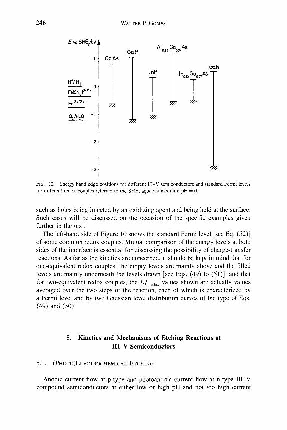
246 WALTER R GOMES
EvsSHE/feVA
H V H 2
FelCNg)^'^
Fe 3*/2*
O2/H2O -1 H
-2]
-3
G a P 0.25 _ 0 7 5
GaAs T
m
InP GaN
In Ga As * "0.53 0/7
#, ^
^ ^
^
FIG. 10. Energy band edge positions for different III-V semiconductors and standard Fermi levels for different redox couples referred to the SHE; aqueous medium; pH = 0.
such as holes being injected by an oxidizing agent and being held at the surface. Such cases will be discussed on the occasion of the specific examples given further in the text.
The left-hand side of Figure 10 shows the standard Fermi level [see Eq. (52)] of some common redox couples. Mutual comparison of the energy levels at both sides of the interface is essential for discussing the possibility of charge-transfer reactions. As far as the kinetics are concerned, it should be kept in mind that for one-equivalent redox couples, the empty levels are mainly above and the filled levels are mainly underneath the levels drawn [see Eqs. (49) to (51)], and that for two-equivalent redox couples, the E^ ^^^^^ values shown are actually values averaged over the two steps of the reaction, each of which is characterized by a Fermi level and by two Gaussian level distribution curves of the type of Eqs. (49) and (50).
Kinetics and Mechanisms of Etching Reactions at III-V Semiconductors
5.1. (PHOTO)ELECTROCHEMICAL ETCHING
Anodic current flow at p-type and photoanodic current flow at n-type III-V compound semiconductors at either low or high pH and not too high current

6 WET ETCHING OF III-V SEMICONDUCTORS 247
densities lead mostly (see subsequent text) to the anodic dissolution and hence to etching of the semiconductor. At high current densities or in the intermediate pH range, the electrochemical oxidation of the semiconductor may lead to pre-cipitation of products upon the surface and hence to passivation of the electrode.
Several studies have been devoted to the electrochemical equivalence of the anodic dissolution reaction, that is, to the number of elementary charges n flow-ing through the external circuit per formula unit of semiconductor dissolved. Values ofn = 6 have been reported for GaAs [8], GaP [32, 33], and InP [34, 35], as well as for the mixed semiconductors Alo25Gao75As [36] and Ino53 Gao47As [37]. It hence follows that in all these cases the elements involved go into solu-tion in the +3 oxidation state. This result is somewhat surprising as far as phos-phorus is concerned, considering the negative standard redox potential of the (H3PO4, H3PO3) couple (t/° = -0.276 V vs. SHE). Since PO^ and PH3 have been detected in solution [32, 38] in the anodic dissolution of GaP, it has been suggested that the H3PO3 or HPO3" formed electrochemically reacts further homogeneously in solution by chemical disproportionation to H3PO4 and PH3. As far as GaN is concerned, recent results demonstrate that n = 3 [31, 39], indi-cating that the oxidation products are Ga in the trivalent state and N2. It should be mentioned that certain authors claim that the photoanodic reaction at n-GaN in aqueous indifferent (H2SO4) electrolyte is H2O oxidation [40]. This appar-ent contradiction in the data may be due to a difference in behavior between the two polar faces perpendicular to the [0001] axis [31] in the sense that, pre-sumably, the N-terminated (0001) face is etched photoanodically, whereas the Ga-terminated (0001) face is not. Whether the free surface is the (0001) or the (0001) face seems to depend on the circumstances under which the GaN film is grown. The growth occurs by MOCVD from (CH3)3Ga and NH3 upon a sap-phire substrate. Gallium-terminated films can apparently be obtained only when, at the initiation of growth, all traces of ammonia have been removed from the reactor.
On the basis of these summarized results and taking into account the chem-istry of the elements involved in strong acidic and alkaline aqueous media [41], the following overall reaction equations can be proposed for the anodic disso-lution of the binary III-V semiconductors under consideration:
At low pH,
GaAs + 2 H2O 4- (6 - jc)h+ -> Ga^+ + HASO2 + 3 H+ + jc e" (69)
GaP -h 3 H2O + (6 - x)h+ -> Ga^+ -f H3PO3 + 3 H+ -h xe' (70)
InP + 3H20 + ( 6 - x ) h + ^ I n ^ + + H3P03-h3H+-hJce- (71)
GaN + (3 - x)h+ -> Ga^+ + ^N2 + xe" (72)

248 WALTER P. GOMES
At high pH,
GaAs + 10 OH- + (6 - jc)h+ -^ GaO^" + ASO2" + 5 H2O + xe" (73)
GaP + 11 OH" + (6 - jc)h+ -^ GaO^" + HPO^" + 5 H2O + jce" (74)
InP + 9 OH" + (6 - jc)h+ -^ InO" + HPO^" + 4 H2O + Jce" (75)
GaN + 6 OH" + (3 - jc)h+ -> GaO^" + ^N2 + 3 H2O + jce" (76)
The symbol x is used to take into account the possible participation of elec-tron injection into the anodic oxidation reaction, a problem that is discussed subsequendy.
In parallel with the foregoing reactions, other reactions may contribute to the anodic current to a minor extent. Thus, an enrichment in As at the GaAs elec-trode surface after anodic current flow has been demonstrated by various exper-imental techniques [42,43]. Hence, it must be concluded that three-equivalent oxidation of GaAs occurs to a small extent in parallel to the six-equivalent oxi-dation. In the intermediate pH range, the formation of an anodic oxide film on the electrode surface is often observed; that is, on GaAs, film formation in a weakly alkaline medium (pH = 11.5) was reported and attributed to slow dis-solution of the Ga203 and AS2O3 formed anodically under these circumstances [44]. Thicker passivating layers on GaAs have been produced under various con-ditions. At n-GaN, a photoanodic current decrease due to Ga203 formation has been observed even in strongly acidic or alkaline media, indicating slow disso-lution kinetics [31]. In view of the scope of this chapter, the focus is primarily on circumstances in which layer formation does not occur.
From various experiments (see subsequent text), it follows that electron injec-tion into the conduction band contributes to the (photo)anodic dissolution reac-tion only to a minor fraction in the case of GaAs [10,45], GaP [33,38,46], and GaN [31]; that is, that JC « 1 in Eqs. (69), (70), (72), (73), (74), and (76). In the case of n-InP, IMPS studies (see Section 2.3) have demonstrated that this fraction depends on the total photocurrent density and may be very significant [47,48]. Indeed, the ratio of the total photocurrent density j vs. the part of it due to hole capture jf^ has been found, for n-InP in an acidic medium, to range from 1.2 at high light intensities [implying JC = 1 in Eq. (71)] to 2 at very low light intensities [implying jc = 3 in Eq. (71)]; see, for example. Figure 11. This means that at low light intensities, three of the six electrochemical steps are hole-capture steps and three are electron-injection steps. At first, this suggests a sequence consisting of a hole-capture step leading to the formation of a radical-type oxidation intermediate, followed by the injection of an electron by that intermediate, again followed by hole capture in a new surface bond, etc. How-ever, from a detailed analysis of the IMPS data [47], it follows that three sub-sequent electron-injection steps are involved, indicating a more complex anodic dissolution mechanism. The decrease in j/jf^ from 2 to 1.2 with increasing light

6 WET ETCHING OF III-V SEMICONDUCTORS 249
logioGh in Acm-2) FIG. 11. Ratio of the total photocurrent density vs. the hole current density, y'/j,,, as a function of the hole current density, 7,,, measured by IMPS at n-InP in 1.2-moI \~^ HCl. The solid and the open symbols refer to measurements on two different electrodes. The curve has been calculated based on the assumptions mentioned in the text. Reprinted from Electwchim. Acta 38, B. H. Erne, D. Vanmaekelbergh, and I. E. Vermeir, pp. 2559-2567, ©1993, with permission from Elsevier Science.
intensity can be understood by assuming that for two electrochemical oxidation steps, a competition exists between electron injection and hole capture, the lat-ter step being increasingly favored when the hole concentration at the surface, and hence the total photocurrent density, increases. The fact that even at very high photocurrent densities one step still occurs exclusively by electron injec-tion leads to the conclusion that for this step, competition with hole capture is absent, the reason presumably being that the corresponding electron level (sur-face state) is located above the conduction band edge. The IMPS data also allow us to estimate the magnitude of the electron-injection rate constants associated with the photoanodic dissolution of n-InP. It was found that in 1-mol \~^ HCl medium, the rate constants are significantly larger (over a factor of 20-200) than in 1.3 mol 1" H2SO4 [48]. Apparently, the presence of CI" ions gives rise to decomposition intermediates with positions more favorable for electron injec-tion as compared to those formed in SO4' containing solutions. It can hence be concluded that the properties of the surface states associated with the anodic decomposition intermediates of In? are influenced by the surface chemistry. The same conclusion follows from the observed enhanced electron-injection rate during photoanodic dissolution of n-InP in the presence of H2O2 [48].
Experimental results obtained at the n-Ino53Gao47As electrode in aqueous 1.3 mol 1~ H2SO4 solution indicate that here, also the contribution of conduction band electron injection to the photoanodic dissolution reaction may be impor-tant when the photocurrent density is low [37]. All this suggests that efficient

250 WALTER R GOMES
electron injection during photoanodic dissolution of III-V compound semicon-ductors may be connected to indium-related surface states.
There are strong indications that, in certain cases, a mixed chemical-electrochemical dissolution mechanism of III-V semiconductors occurs. As far back as 1969, Gerischer et al. [10,11] reported an accelerating effect of Br2 upon the anodic dissolution of p-type GaAs, in the sense that the onset of the anodic current density curve was shifted toward less positive potentials as compared to the curve in an indifferent electrolyte. If the position of the band edges is unaffected by adding the oxidizing agent, this implies that at the same band-bending (i.e., the same hole concentration at the surface pj the anodic current and hence the corresponding rate constant is larger (see Section 2). The authors interpreted this effect as follows. It is generally accepted that the first hole-capture step in the anodic oxidation reation is rate-determining as a conse-quence of the high activation energy for breaking an intact surface bond. Since Br2 is known to be a chemical etchant for GaAs, Gerischer et al. then assumed that, in the presence of Br2, the slow first electrochemical step is substituted by a faster chemical bond-breaking step (or more likely, that the first two steps are substituted). Afterward, the same effect was observed with several other systems, including p-GaP-aqueous Br2 [49], p-GaP-methanoHc Br2 [50], and p-InP-aqueous HIO3 [51]. Such a negative shift of the anodic dissolution curve may serve as an indication that the oxidizing agent involved acts as a chemi-cal etchant under open-circuit conditions. It should be checked by performing impedance measurements, however, whether the observed shift is due to an arte-fact, that is, to a shift in flat-band potential caused by the interaction of the oxi-dizing agent with the semiconductor surface. A particularly interesting case is that of p-GaP-Br2 in methanol [50]. By adding Br2 to the methanolic solution, the anodic dissolution curve of ( i l l ) p-GaP was found to shift up to 0.6 V on the potential scale referred to the flat-band potential, indicating that the preced-ing interpretation holds. At the (111) p-GaP face, however, no such effect was observed, in agreement with the observation that the open-circuit rate of etching by Br2 at the (111) face is much lower than at the opposite polar face [i.e. the ( i l l ) face]. However, rotating ring-disk experiments showed an increased Br2 consumption at the (111) face under anodic current flow. Moreover, the electro-chemical equivalence of the anodic dissolution reaction was found to be about 4 in the presence of Br2, in contrast to the value of 6 measured in an indifferent electrolyte. All these data strongly indicate that a mixed dissolution mechanism holds here also, but the first oxidation steps are hole-capture steps, and two fur-ther steps are chemical; that is, chemical attack of the (111) face by Br2 can occur only after bond cleavage has been initiated by holes.
It is evident that formulas such as Eq. (69) or (73) merely describe the overall anodic etching reactions and that these reactions involve various decomposition intermediates as well as chemical steps in which (in an aqueous medium) H2O molecules or 0H~ ions participate. Several experimental approaches based on

6 WET ETCHING OF III-V SEMICONDUCTORS 251
electrode kinetics have been used to obtain more detailed information on the anodic or photoanodic dissolution mechanisms of III-V semiconductors.
One of these approaches consists of studying the kinetics of the competition between the (photo)anodic dissolution reaction of the semiconductor and the capture of holes by a one-equivalent reducing agent such as the Fe^^ ion or a Fe(II)-based complex. Interest in this subject was originally connected with the field of electrochemical solar energy conversion. Indeed, in 1975, Gerischer [52] proposed a type of solar cell based on a semiconductor electrode, called a regenerative or photovoltaic electrochemical cell, in which a dissolved reduc-ing agent was photoanodically oxidized by holes at an n-type semiconductor electrode, while the corresponding oxidizing agent was reduced back at a dark counterelectrode, the net result being the conversion of solar energy into elec-trical energy. In view of the matching of the bandgap of the semiconductor with the spectral distribution of sunlight, GaAs and InP seemed to be the most suitable candidates for use as photoactive electrode materials. However, it was soon realized that one of the main problems with such cells was the stability of the semiconductor material with respect to photocorrosion, that is, in addition to hole capture by the dissolved reducing agent, reactions such as (69) or (71) take place also. To optimize the competition between both reaction types in favor of the added reducing agent, thorough kinetic studies were made in which the competing rates were investigated as a function of reducing agent concen-tration, pH, solvent composition, and light intensity. These investigations were carried out mainly by rotating ring-disk measurements; see Section 2.2. For a review on the results, see, for example, [13]. The fact that in nearly all cases the competition was more in favor of the photoanodic dissolution reaction when the light intensity was higher turned out to be an especially important clue as far as the competition mechanism is concerned. Indeed, if both reactions were simply occurring in parallel, they both would be first order in photogenerated holes [see Eqs. (44) and (60)], so that the competition would be light-intensity independent. A detailed analysis revealed the central role of the decomposition intermediate X^, formed when an intact surface bond of the semiconductor cap-tures a hole from the valence band. For example, for GaAs,
GaAs + h + ^ X + (77)
where Xf is a surface bond with one electron missing. Many of the kinetic data could be explained by assuming that the dissolved reducing agent is not oxi-dized by a hole, but by donating an electron to X^, hence restoring the surface bond. More importantly in the present context, in most cases involving GaAs the kinetics indicated that the intermediate X^ and not the free hole h" consti-tutes the mobile species participating in the consecutive steps of the dissolution reaction, so that it must be concluded that the intermediate X^ is mobile within a two-dimensional layer; in other words, that a bonding electron may jump from an unbroken surface bond to a neighboring electron-deficient bond.
252 WALTER P. GOMES
More insight into the surface chemistry involved in the anodic dissolution reaction was obtained by studying the competition kinetics under conditions of varying pH and water activity, the latter being varied by adding large con-centrations of a highly hydrated salt such as LiCl or by using mixed solvents such as water-methanol or water-acetonitrile. The results, which were primar-ily obtained on GaAs and GaP, led to a comprehensive model, proposed in [53]. The model assumes that after reaction (77), a chemical reaction between Xf and water occurs:
X+ + mH^O ^ Xi—OH + H+(H20)^_i (78)
In this reaction, m water molecules react with the mobile and positively charged intermediate X^, giving rise to a neutral intermediate X^—OH and a solvated proton. The intermediate X^—OH is then supposed to be immobile since it con-tains an OH group attached to the surface. The equilibrium (78) is thought to play a key role in the dissolution mechanism. For GaAs in an acidic aqueous medium, this equilibrium is supposed to be positioned somewhere in the mid-dle, so that the second step of the photoanodic dissolution reaction is between Xi—OH and X^. In contrast, for GaP, this equilibrium is assumed to be posi-tioned far to the right (i.e., practically no mobile intermediates are available), so that here the second oxidation step is between X^—OH and a free hole. The observed changes in competition mechanism induced by decreasing the water activity can then be explained as consequences of equilibrium (78) being shifted toward the left.
The conclusions just mentioned were largely confirmed from independent data obtained by quantitatively studying the enhancement of the anodic dark current density at n-type electrodes, caused by hole injection. Indeed, as mentioned in earlier sections, under anodic bias, holes injected into an n-type semiconductor by an oxidizing agent in darkness are consumed, just like at rest potential, in the anodic dissolution reaction of the semiconductor. If the latter reaction involves the valence band solely, the anodic blocking current will remain unchanged by adding the hole-injecting reactant. Any participation of conduction band electrons in the dissolution reaction will show up as an increase in the dark anodic limiting current density. By this method, it has been demonstrated that the conduction band contributes considerably to the anodic dissolution reaction in the case of InP and IUQ 53Gag 47 As (as confirmed later by IMPS measurements; see preceding text), but only to a minor fraction (on the order of per thousand to per hundred) to the anodic dissolution of GaAs and GaP. Because j ^ , the anodic current density increase, was found to increase with temperature (for GaAs and GaP) [45,46], this process is believed to be activated; that is, the electron must be thermally excited from the surface state associated with the decomposition intermediate to the conduction band before injection can occur.
Measuring the relationship between the additional anodic current density j^ and the cathodic hole injection current density j^ constitutes a powerful probe

6 WET ETCHING OF III-V SEMICONDUCTORS 253
for investigating the dissolution mechanism. The basic assumption used in the interpretation of such relationships, obtained on GaAs and GaP, is that the anodic current increase is due to injection of an electron by the first decom-position intermediate, X^, into the conduction band. Analysis of the results by standard steady-state kinetic treatment then leads to conclusions that confirm those obtained by studying the competition kinetics [54].
Recall at this point that anodic electron injection by dissolution intermedi-ates can be observed not only as a consequence of hole injection (i.e., of elec-troless etching), but alternatively as a consequence of chemical etching (see Sections 3.4 and 5.4). Analogously, as before, quantitative studies of the rela-tionship between the injection current density j^ and the chemical etch rate may yield important information on the etching mechanism, as will be shown further.
5.2. PHOTOETCHING
The simple model for electroless photoetching, as proposed in Section 3.2, appears to hold in the case of the InP-Fe^^ system in an acidic medium [55, 56]. The partial current densities at the rest potential were determined as follows. The illuminated n- or p-type InP electrode in an Fe^^-containing solution was held at the potential at which the net current was zero (rest potential). Then the light was abruptly shut off. The value of the current density immediately after interruption of the light yields the partial "dark" current density, corresponding to cathodic Fe " reduction in the n-type case and to anodic dissolution of the InP in the p-type case (see Fig. 7). The reason the light has to be shut off abruptly is that the energy bands may shift under illumination, so that the "dark" partial current density under illumination may be different from that in darkness. An alternative procedure consists of working with chopped light (see subsequent text). The (photo)anodic partial electrical current density at rest potential j^^ was then compared to the photoetch rate, the latter being determined analytically. To enable the comparison between both quantities, the photoetch rate rgj h was converted into an etch current density j^^^^ through the relationship
y'etch = «^^etch C79)
where n is the number of charge carriers involved in the anodic dissolution of one formula unit of InP, equal to 6 [see Eq. (71)]. Figure 12 demonstrates the good quantitative correlation between the electrical and the etch current densities and hence the validity of the simple photoetch model of two compensating partial currents. Also according to this model, the photoetch rate is expected to be higher as the onset of the anodic dissolution curve is shifted toward negative potentials and the onset of the cathodic reduction curve is shifted toward positive potentials. This prediction is fulfilled in the given case, because the photoetch rate was found to be considerably higher in a HCl medium than in H2SO4 or

254 WALTER R GOMES
. etch , . -2 / / M.A.cm
PI -2
FIG. 12. Photoetch current density obtained form etch rate measurements, jf^, vs. partial electrical current density, jf measured at rest potential at n-InP in aqueous FeCl3 +HC1 (pH = 0). O, (111) face; A, (111) face. Reprinted from J. Electrochem. Soc. 142, I. E. Vermeir, W. P. Gomes, and P. Van Daele, pp. 3226-3232, 1995. Reproduced by permission of the Electrochemical Society, Inc.
in HCIO4, and corresponding voltammetric results show that in a HCl medium, both currents are shifted favorably as compared to H2SO4 or HCIO4 media. Considering the general reaction scheme for simple photoetching [Eq. (66)], the anodic reaction here is Eq. (71) and the cathodic reaction is
Fe^++e- Fe 2+ (80)
In view of the discussion in Section 7, it is worth mentioning that at the same light intensity, the photoetch rate at the (111) face is much lower than that at the ( i l l ) face [56]. This difference between both polar faces is well known for dark etching, but rather surprisingly holds as well for photoetching in the given case.
Results similar to those outlined previously were obtained for GaP in alka-line OBr~ solution [57]. The partial reactions are now Eq. (74) and the reduction of OBr~, which appears to involve the current-doubling mechanism

6 WET ETCHING OF III-V SEMICONDUCTORS 255
200
100
0
•100
-200
.inn
-
y
Voc
r.
^ ..A^dfiil
a
-1.2 -1.1 -0.9 -0.8 -0.7 -0.6 -0.5 -0.4 Vvs.SCE l\/
-0.3
FIG. 13. Voltammograms, obtained at n-GaN in aqueous 1-mol 1"' KOH with chopped illumi-nation. Curve a, light off; curve b, light on. V^ is the open-circuit potential under illumination. Courtesy of I. M. Huygens, unpublished results.
(see Section 2.4):
OBr- + e + H2O ^ Br* + 2 OH"
Br* -> B r + h +
(81)
(82)
Also in the case of (0001) n-GaN, photoetching can be achieved in aque-ous alkaline-indifferent electrolyte [31]. This is visualized in Figure 13, which shows voltammetric results in 1-mol 1" KOH obtained with chopped illumina-tion. Curves a and b connect the points with the light off and on, respectively. The potential indicated in the figure represents zero net current under illumina-tion. This situation results from two mutually compensating currents, that is, the dark cathodic current and the photoanodic dissolution current, corresponding to reaction Eq. (76), the net result being the photoetching of GaN. The oxidizing agent in indifferent electrolyte is H2O and/or residual dissolved O2. This pho-toetching effect is essentially due to the fact that the onset of the dark cathodic j vs. V curve is situated in a potential range that is markedly positive with respect to the flat-band potential, implying a very high reactivity of conduction band electrons toward the oxidizing agent. Note that in acidic media, no such

256 WALTER P. GOMES
high reactivity of conduction band electrons occurs and hence no photoetching of GaN is observed. Presumably, a special reaction pathway exists in alkaline media through surface states, the presence and/or activity of which is somehow controlled by the surface chemistry.
Due to the high chemical stability of GaN, etching recipes for this semicon-ductor material are scarce, so the proposed photoetching procedure constitutes an interesting possibility for wet processing of GaN in device technology. We recall, however, that it is very likely that this possibility may not exist as far as the (0001) face is concerned, because the photoanodic current does not involve dissolution of the GaN (see Section 5.1).
Photoetching processes do not always consist of a simple superposition of an anodic and a cathodic partial process, and may exhibit various types of com-plications. First, even in the "simple" case of the photoetching of GaP single crystals in alkaline OBr~ solutions, the situation is actually more complex than depicted, because in n-type crystals, the photoetching process itself induces a hole injection reaction and hence an electroless etching effect [57]. Initially, OBr" is reduced at the GaP surface via the previously mentioned current-doubUng mechanism. However, during the reduction of OBr~ ions, Br* radicals are formed as intermediates [cf. reaction (81)], which appear to initiate an auto-catalytic reaction mechanism: surface states are formed, through which holes are injected into the valence band (at least at not too high OBr~ concentra-tions). These surface states, which are experimentally detected as a peak in the capacitance-potential plot [57, 58], are believed to be associated with adsorbed OBr". Furthermore, voltammetric experiments demonstrate that these surface states can be annihilated by a sufficiently large concentration of holes at the sur-face. The latter effect may explain why this induced electroless etching effect is not observed at p-GaP, since in this case the holes are the majority carriers.
Another more complicated case is the photoetching of GaAs by several two-or multiequivalent oxidizing agents such as H2O2, Br2, OBr", OCl", S208~, and Cr03-HF [12,59-66]. The mechanisms of the etching reactions appear to be rather complex. The oxidizing agent was found to react at the semiconduc-tor through various pathways, such as chemical etching, hole injection, electron capture followed by hole injection (current doubling), and hence photoetching. A model has been proposed in which these reactions were supposed to be mutu-ally linked via a common precursor, that is, a chemisorbed surface complex formed by transfer of an electron from a surface bond to the oxidizing agent. A more detailed discussion on the competing reactions subsequent to the for-mation of the precursor will be given later in this chapter.
Particularly interesting features have been observed in the photoetching of n-GaAs surfaces that are partially illuminated with laser Ught [65,66]. Photoetching occurs only at the illuminated spots with a quantum efficiency that is considerably higher than under uniform illumination (in the latter case, the quantum efficiency is usually low because the rest potential is generally situ-ated in the onset region of the photocurrent curve; see Figure 7). The quantum
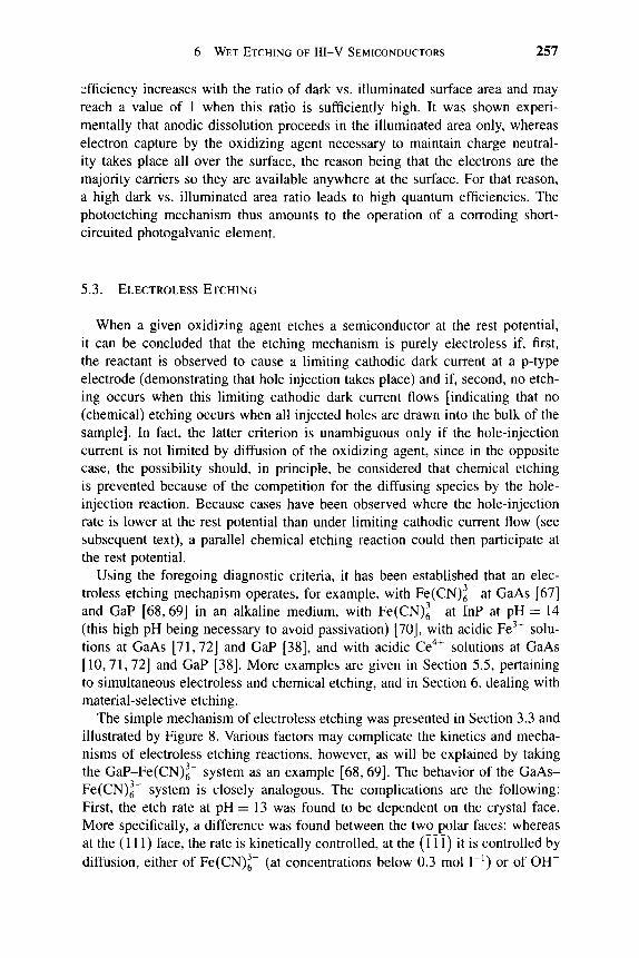
6 WET ETCHING OF III-V SEMICONDUCTORS 257
efficiency increases with the ratio of dark vs. illuminated surface area and may reach a value of 1 when this ratio is sufficiently high. It was shown experi-mentally that anodic dissolution proceeds in the illuminated area only, whereas electron capture by the oxidizing agent necessary to maintain charge neutral-ity takes place all over the surface, the reason being that the electrons are the majority carriers so they are available anywhere at the surface. For that reason, a high dark vs. illuminated area ratio leads to high quantum efficiencies. The photoetching mechanism thus amounts to the operation of a corroding short-circuited photogalvanic element.
5.3. ELECTROLESS ETCHING
When a given oxidizing agent etches a semiconductor at the rest potential, it can be concluded that the etching mechanism is purely electroless if, first, the reactant is observed to cause a limiting cathodic dark current at a p-type electrode (demonstrating that hole injection takes place) and if, second, no etch-ing occurs when this limiting cathodic dark current flows [indicating that no (chemical) etching occurs when all injected holes are drawn into the bulk of the sample]. In fact, the latter criterion is unambiguous only if the hole-injection current is not limited by diffusion of the oxidizing agent, since in the opposite case, the possibility should, in principle, be considered that chemical etching is prevented because of the competition for the diffusing species by the hole-injection reaction. Because cases have been observed where the hole-injection rate is lower at the rest potential than under limiting cathodic current flow (see subsequent text), a parallel chemical etching reaction could then participate at the rest potential.
Using the foregoing diagnostic criteria, it has been established that an elec-troless etching mechanism operates, for example, with Fe(CN)^~ at GaAs [67] and GaP [68,69] in an alkaline medium, with Fe(CN)6" at InP at pH = 14 (this high pH being necessary to avoid passivation) [70], with acidic Fe^^ solu-tions at GaAs [71,72] and GaP [38], and with acidic Ce" ^ solutions at GaAs [10,71,72] and GaP [38]. More examples are given in Section 5.5, pertaining to simultaneous electroless and chemical etching, and in Section 6, dealing with material-selective etching.
The simple mechanism of electroless etching was presented in Section 3.3 and illustrated by Figure 8. Various factors may complicate the kinetics and mecha-nisms of electroless etching reactions, however, as will be explained by taking the GaP-Fe(CN)^~ system as an example [68,69]. The behavior of the GaAs-Fe(CN)^~ system is closely analogous. The complications are the following: First, the etch rate at pH = 13 was found to be dependent on the crystal face. More specifically, a difference was found between the two polar faces: whereas at the (111) face, the rate is kinetically controlled, at the (111) it is controlled by diffusion, either of Fe(CN)^~ (at concentrations below 0.3 mol 1" ) or of OH"
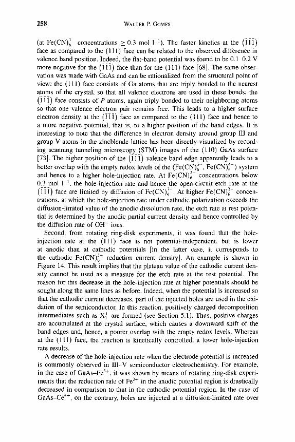
258 WALTER P. GOMES
(at Fe(CN)6~ concentrations > 0.3 mol \~^). The faster kinetics at the (111) face as compared to the (HI) face can be related to the observed difference in valence band position. Indeed, the flat-band potential was found to be 0.1-0.2 V more negative for the ( i l l ) face than for the (HI) face [68]. The same obser-vation was made with GaAs and can be rationalized from the structural point of view: the (HI) face consists of Ga atoms that are triply bonded to the nearest atoms of the crystal, so that all valence electrons are used in these bonds; the ( i l l ) face consists of P atoms, again triply bonded to their neighboring atoms so that one valence electron pair remains free. This leads to a higher surface electron density at the ( i l l ) face as compared to the (HI) face and hence to a more negative potential, that is, to a higher position of the band edges. It is interesting to note that the difference in electron density around group III and group V atoms in the zincblende lattice has been directly visualized by record-ing scanning tunneling microscopy (STM) images of the (110) GaAs surface [73]. The higher position of the ( i l l ) valence band edge apparently leads to a better overlap with the empty redox levels of the (Fe(CN)^~, Fe(CN)^~) system and hence to a higher hole-injection rate. At Fe(CN)^~ concentrations below 03_mo\ ^ ^ the hole-injection rate and hence the open-circuit etch rate at the ( i l l ) face are limited by diffusion of Fe(CN)6". At higher Fe(CN)^~ concen-trations, at which the hole-injection rate under cathodic polarization exceeds the diffusion-limited value of the anodic dissolution rate, the etch rate at rest poten-tial is determined by the anodic partial current density and hence controlled by the diffusion rate of 0H~ ions.
Second, from rotating ring-disk experiments, it was found that the hole-injection rate at the (HI) face is not potential-independent, but is lower at anodic than at cathodic potentials [in the latter case, it corresponds to the cathodic Fe(CN)^~ reduction current density]. An example is shown in Figure 14. This result implies that the plateau value of the cathodic current den-sity cannot be used as a measure for the etch rate at the rest potential. The reason for this decrease in the hole-injection rate at higher potentials should be sought along the same lines as before. Indeed, when the potential is increased so that the cathodic current decreases, part of the injected holes are used in the oxi-dation of the semiconductor. In this reaction, positively charged decomposition intermediates such as Xf are formed (see Section 5.1). Thus, positive charges are accumulated at the crystal surface, which causes a downward shift of the band edges and, hence, a poorer overlap with the empty redox levels. Whereas at the (111) face, the reaction is kinetically controlled, a lower hole-injection rate results.
A decrease of the hole-injection rate when the electrode potential is increased is commonly observed in III-V semiconductor electrochemistry. For example, in the case of GaAs-Fe^^, it was shown by means of rotating ring-disk experi-ments that the reduction rate of Fe^^ in the anodic potential region is drastically decreased in comparison to that in the cathodic potential region. In the case of GaAs-Ce"^" , on the contrary, holes are injected at a diffusion-limited rate over

6 WET ETCHING OF III-V SEMICONDUCTORS 259
/7 m A.cm' 0
-0.4
T3 - 0 . 8 o
J C
r 2
-u
-1.6h
n—
r 1/
I
'—1 u-^:???^-
/^"[y^''
J ! 1 1 1 L.
=T
- L . — L - 1 1
\
—L-J -1.5 -1.0
VvsSOEIM -0.5
FIG. 14. Current density vs. potential curves at (111) n-GaP in aqueous 10~^-mol 1" K3Fe(CN)6 + 0.1-mol r^ KOH. —, net current density; - - -, partial current density due to reduction of Fe(CN)6". Reprinted from Electrochim. Acta 35, H. H. Goossens, I. E. Vermeir, F. Vanden Kerchove, and W. P. Gomes, pp. 1351-1358, ©1990, with permission from Elsevier Science.
the whole potential region [71, 72]. This difference in behavior is explained on the basis of the positions of the redox levels concerned. Whereas the (Ce ^ , Ce " ) standard Fermi level lies well below the valence band edge, the (Fe^^, Fe " ) standard Fermi level is located close to the valence band edge, so that the overlap of the unoccupied (Fe^^) levels with the valence band, and hence the Fe " reduction rate, is very sensitive to the downward displacement of the valence band edge under anodic polarization caused by the accumulation of holes at the surface.
5.4. CHEMICAL ETCHING
In a chemical etching mechanism, no free charge carriers (no valence band holes) are involved. Whereas most chemical etchants for III-V compound semi-conductors are oxidizing agents, just as electroless etchants are, it is essential to distinguish between the two dark etching mechanisms. The obvious way to do this is by observing the cathodic behavior of the p-type semiconductor in darkness in the presence of the etchant: if no cathodic reduction of the etchant (hence no hole injection) occurs, the etching mechanism cannot be electroless and, hence, must be chemical.
In addition to allowing a decision on whether the etching mechanism is elec-troless or chemical, electrochemical measurements also yield essential informa-tion on chemical etching reactions, that is, on the stoichiometry of the surface reaction, on the problem of whether the mechanism is concerted (synchronous) or sequential, etc. This information will be explained by taking a study on the

260 WALTER R GOMES
etching of GaP by methanolic bromine solution [50,74] as an example. This solution is commonly used for the etching various III-V and II-VI semiconduc-tor materials. Considering that bromine-methanol mixtures may be hazardous at high Br2 concentrations [75] and that methanol is toxic, one of the main objectives of this study was to find the possible advantages of using methanol instead of water as the solvent for bromine-based etching solutions.
Measurements were performed at the ( i l l ) and the (111) GaP face. At the rest potential, the etch rate at the (111) face appeared to be diffusion-limited, whereas that at the (111) face was low and independent of the rotation rate of the sample. The etch rate under given circumstances was the same for n- and p-type samples. The etch rate and the current density at the ( i l l ) face were studied at an n-type ( i l l ) GaP electrode as a function of electrode potential. The results are represented in Figure 15. A cathodic diffusion-controlled plateau is observed at sufficiently negative potentials. In this potential region, the etch rate is low. In Figure 15, the etch rates have been converted into etch current densities, based on Eq. (79), in which n has been put equal to 6. The underlying hypothesis here is that, similar to the anodic dissolution, the oxidation of GaP by Br2 is a 6-equivalent redox reaction. When the electrode potential is increased, the cathodic current decreases and, simultaneously, the etch rate increases. Finally, at sufficiently positive potentials, a low limiting anodic current is observed and
rofe/mA.cm"2
2.5i
-5
^^^ K \
L -_^,—• • J
-0.8 -0.6 -O.A -0.2 0.2 0.A
Vvs.AglAgCilCr/si
FIG. 15. Combined etch rate and current density vs. potential plots at ( i l l ) n-GaP in methanolic 4 x 10~^-mol r^ Br2+0.25-mol \~^ LiCl. x, etch rate (expressed as an etch current density); •, electrical current density. Reprinted from J. Electrochem. Soc. 140, K. Strubbe and W. P. Gomes, pp. 3294-3300, 1993. Reproduced by permission of The Electrochemical Society, Inc.

6 WET ETCHING OF III-V SEMICONDUCTORS 261
the etch rate reaches a Umiting value that is proportional to the square root of the rotation speed of the electrode. The sum of the etch rate and the absolute value of the electrical current density is found to be constant over the entire potential range. Rotating ring-disk experiments show that the Br2 consumption at the GaP disk is potential-independent and equal to the diffusion-controlled value.
Measurements at the p-type ( i l l ) face show that Br2 is not reduced cathod-ically in darkness, which allows us to exclude electroless etching. Combined current-potential and impedance measurements reveal that the anodic dissolu-tion current starts at a considerably lower surface hole concentration in the pres-ence of Br2 than in an indifferent electrolyte solution. Also this phenomenon points to a chemical etching mechanism, since it can be explained by assuming that in the presence of Br2, the first (slow) anodic dissolution steps are replaced by faster chemical steps; the faster subsequent hole-capture steps can then occur at a higher rate for the same hole concentration than in a totally electrochemical mechanism (see Section 5.1).
The fact that the cathodic limiting current density j^y^^^ in Figure 15 is found to be equal to the anodic limiting etch current density yetch,iim confirms that this chemical etching process is a 6-equivalent redox reaction, as assumed. Indeed, because the cathodic reduction of Br2 is 2-equivalent, j^ ,jn, can be written as
l,,^ = 2FJ^,^ (83)
where J^^^ is the diffusion flux of Br2 toward the electrode surface. Putting Eq. (83) equal to yet,h,iim = ^Fr,,^hMm yields
^Br2 — ^ '"etch, lim \^^)
that is, the number of moles of Br2 arriving at the surface by diffusion is 3 times the number of moles of GaP consumed. Taking into account chemical considerations [76,77], the reaction equation can then be proposed as
O t
GaP + 3 Br2 + 3 CH3OH -> GaBr3 + (CH30)2 P—H + CH3Br -h 2 HBr (85)
Note that the experiments mentioned yield direct information on the stoichiom-etry of the surface reaction and that it cannot be excluded that (CH30)2PHO is further oxidized by Br2 homogeneously in solution.
The fact that a small limiting current due to the presence of Br2 is observed anodically at ( i l l ) n-GaP allows us to conclude that the etching mechanism is not concerted, but sequential. Indeed, this anodic current can be attributed to electron injection by decomposition intermediates of GaP; see Section 5.1. If the chemical etching mechanism were synchronous, no such intermediates would be formed. More details on the reaction mechanism can be obtained by studying the relationship between this limiting anodic current and the consumption rate

262 WALTER P. GOMES
|;^l/mA.cm"2
FIG. 16. Anodic j^ vs. cathodic \j^\ current density at ( i l l ) n-GaP in methanolic LiCl +various Br2 concentrations; V^ and V^ equal 0.4 and -0.8 V vs. Ag-AgCl-Cl", respectively. The closed symbols refer to 0.25 mol \~^ LiCl; the open ones refer to 4-mol 1"' LiCl. Reproduced from J. Electrochem. Soc. 140, K. Strubbe and W. P Gomes, pp. 3294-3300, 1993. Reproduced by permission of The Electrochemical Society, Inc.
of Br2. As appears from the considerations mentioned previously for the latter, the cathodic Hmiting current density can be taken as a measure. Figure 16 shows the measured relationship between the anodic and the cathodic limiting current densities at two different concentrations of the indifferent electrolyte (LiCl). The relationship appears to be linear in both cases and the slope is lower at higher LiCl concentration. These data can be interpreted as follows [74]. Reaction of an unbroken surface bond with Br2 first leads to the formation of a mobile surface intermediate X^:
GaP + Br2 -> X+ + Br" -f Br* (86)

6 WET ETCHING OF III-V SEMICONDUCTORS 263
(see Section 5.1). In the next step, the positively charged X^ intermediate is converted into an immobile neutral intermediate Xj—A by the reaction
K X+ + A- ^ X|—A (87)
In principle, A~ may be either CI", present in the indifferent electrolyte solution, or Br~, formed during the chemical etching process [Eq. (86)], or methanolate [in which case a proton is released in reaction (87)]. Whereas P is more elec-tronegative than Ga, the A~ anion is localized on the gallium.
We assume that the equilibrium (87) is positioned to the right, so that few mobile Xf intermediates are present. The neutral species Xj—A is then further oxidized by the Br* radical to the intermediate X^:
Xi—A + Br*-^X2+ + Br- (88)
The anodic current increase is attributed to electron injection from Xf into the conduction band of the semiconductor, occurring in parallel with reaction (87):
X ^ - ^ X ^ ' ^ + e - (89)
Whereas the chemical structure of the intermediate X\^ is obviously different from that of Xj , step (89) must be followed by other chemical reaction steps. However, since these steps do not influence the competition between reactions (87) and (89), they are not taken into account in the kinetic derivation.
Further oxidation of the semiconductor is then assumed to proceed in subse-quent steps, in which two more Br2 molecules per GaP formula unit are con-sumed. The small excess of Br* at the surface [formed during reaction (86), but not used up in reaction (89), since X^ is converted into X^^ in reaction (89) without consumption of Br*] is assumed to desorb from the surface and to react further in solution:
Br* ^ (Br-),„„ (90)
By a standard steady-state kinetic derivation, the proposed mechanism is shown to lead to the following relationship between the anodic current density j^ and the cathodic current density \j^\\
i = ^ ek,k_XcA .g^.
in which c^ represents the concentration of A. Equation (91) predicts a linear relationship between j^ and \j^\ for the ( i l l )
face with a positive intercept on the j^ axis, as is found experimentally (Fig. 16). Equation (91) also predicts that an increase of the A concentration leads to a
264 WALTER P. GOMES
decrease of the slope of the j^ vs. |7^| curve. In Figure 16, we see that the slope of the j^ vs. \j^\ plot in 4-mol 1" LiCl is lower than in 0.25-mol T^ LiCl, indicating that step (87) occurs between X^ and a CI" ion in that case. In practical etching conditions in which no LiCl is present, the anion reacting with Xf is presumably the Br~ ion formed in the first step.
When comparing the results of this study on the etching of GaP by methanolic Br2 to those by aqueous Br2 [49], it appears that both processes occur quite similarly. Hence, there seems to be no clear advantage of using methanol as the solvent, except maybe for the fact that the solubility of bromine is higher in methanol than in water. However, especially at high concentrations, bromine solutions in methanol are hazardous. Moreover, it is possible to increase the solubility of bromine in aqueous solutions considerably by complexing it with bromide to form Br^ and Br^.
Other oxidizing substances besides Br2 that usually act as chemical etchants for III-V compound semiconductors are CI2, I2, OCP, H2O2, and HIO3. Most often it is found that the etch rate at the (100) and ( i l l ) faces is comparable, whereas that at the (111) face is considerably lower. The difference in kinetics between both polar faces perpendicular to the [111] axis has been attributed to the fact that electrophilic reactants are concerned and that the electron density at the ( i l l ) face is higher than that at the (111) face, due to the difference in orientation of the group III atom-group V atom surface dipole [78,79]. By exception, the chemical etch rate of InP by HIO3 is diffusion-controlled even at the (111) face [51]; otherwise, the electrochemical and etching behavior of this system is quite similar to that of GaP-methanolic Br2 described previously.
Kelly and co-workers performed extensive studies on the etching of GaAs in acidic solutions containing CI2, Br2, I2, or H2O2 [60,61] and in alkaUne solu-tions containing the hypohalites C10~ and BrO~ [62]. Their observations will be examplified by the case of GaAs-H202. An enhanced anodic dark current at n-type electrodes in the presence of the oxidizing agent was observed, as was an interdependence between the rate of chemical etching and that of cathodic reduction. Indeed, in darkness, the cathodic current at a p-type electrode is low, indicating weak hole injection by the oxidizing agent. Under the same cir-cumstances, GaAs is etched at a potential-independent rate. When the p-type electrode is illuminated, a photocurrent is observed that involves the current-doubling mechanism (see Section 2.3), and the etch rate decreases by a corre-sponding amount. At high light intensities, the etching is completely suppressed cathodically even though no significant depletion of the oxidizing agent at the surface occurs. The conclusion was reached that hole injection, electron cap-ture, and chemical etching are coupled through a common precursor: the oxi-dizing agent is thought to adsorb on the semiconductor surface under injection of a hole in a surface bond, so that an electron-deficient species of the type as depicted in Figure 17 is formed. Electronically, this species acts as a filled sur-face state, the electron of which can be injected into the conduction band or can participate in competing surface reactions (see the scheme of Figure 17, which

6 WET ETCHING OF III-V SEMICONDUCTORS 265
H^Oo • Ga:As '
<A 'OH OH® "OH OH® OH
Ga:As * OH • h < ^ Go® . As - ^ Go® As
(DJ« •OH
® ^Ga : As '^ * OH®
®1 OH^
FIG. 17. Unified model for cathodic reduction of H2O2 at GaAs and chemical etching of GaAs in H2O2 solutions. Reproduced from J. Electroanal. Chem. 273, B. P. Minks, D. Vanmaekelbergh, and J. J. Kelly, pp. 133-145, ©1989, with permission from Elsevier Science.
represents the unified model proposed for these competing reactions). Although at first, this common precursor looks similar to the species X^—CI proposed in the work on GaP-methanolic Br2 (see preceding text), there is a significant difference. Indeed, the intermediate represented in Figure 17 may be viewed as an immobilized hole, complexed with the anion that results from the etchant (0H~, B r ~ , . . . ) that, in a subsequent step, may react with the adsorbed radi-cal (OH*, Br* , . . . ) . Chemical reaction with CI" should hence not occur, and the C r concentration should not influence the injection rate, in contrast to the experimental evidence in the case of GaP-methanolic Br2 (Fig. 16).
Hydrogen peroxide is a very common etchant for GaAs in device fabrication. Several studies have been devoted to the etching mechanisms in different pH ranges. Kelly and Reynders [80] investigated the etching of GaAs in dilute aque-ous H2O2 solutions in the higher pH range. Above pH = 12, where electrolytic dissociation of H2O2 to H^ and HO^ takes place, the etch rate is low. Below pH = 10, etching is prevented by the formation of a Ga-rich oxide film on the GaAs surface. In the intermediate pH range, the etch rate is kinetically con-trolled. These findings were interpreted on the basis of a mechanism in which, first, the GaAs is oxidized by undissociated H2O2 molecules to As(III), which goes into solution, and to adsorbed Ga(0H)3. In a second step, Ga(0H)3 is desorbed. Depending on the pH, either the oxidation step or the desorption step is rate-determining. Similar reaction schemes involving oxidation and desorp-tion have also been proposed for the etching of GaAs by H2O2 in acidic media [81-83].
The etch rate of GaP by H2O2 has found to be rather low [57]. The etching of InP by H2O2 also occurs at a low rate [48].

266 WALTER P. GOMES
The etching behavior of InP is different from that of other III-V semicon-ductors in that InP is etched in concentrated aqueous HCl or HBr solutions [84, 85]. A significant etch rate is observed only at HCl or HBr concentrations above 5 mol 1"^ This strongly suggests that the etch rate depends on the degree of dissociation of the HCl or the HBr, and that, in fact, undissociated hydrogen halide molecules are involved. This hypothesis is confirmed by results obtained with HCl dissolved in acetic acid. Whereas the dissociation constant of HCl in CH3COOH is many orders of magnitude lower than in water, undissociated HCl molecules are the prevailing species in acetic acid solutions, even at low HCl concentrations. Experiments in that medium show that the etch rate of InP is proportional to the HCl concentration, confirming that HCl molecules, and not protons, are the active species. Whereas neither HCl nor HBr is an oxidizing agent, the etching mechanism must be chemical and synchronous as depicted in Eq. (68) as far as the first step is concerned. This step is very likely the rate-determining one. To complete the dissolution of one formula unit of InP, two more HCl or HBr molecules are necessary; the end products are PH3 gas and InCl3 or InBr3, which may undergo further hydrolysis reactions.
It is important to note that InP is normally covered by a native oxide layer, which is also removed in the HCl or HBr solutions used as etchants.
Since the etching mechanism is not sequential, no enhancement of the limiting anodic dark current at n-type InP electrodes upon addition of concentrated HCl solution is expected, because no decomposition intermediates are formed. This expectation appears to be fulfilled experimentally [51]. We recall here that if decomposition intermediates were formed, the electron-injection effect would be substantial in the case of InP (see Section 5.1).
A final remark is that it is hitherto not clear why InP is etched in concentrated HCl or HBr solutions, whereas other III-V compound semiconductors such as GaAs and GaP are not.
5.5. ELECTROLESS AND CHEMICAL ETCHING
OCCURRING IN PARALLEL
Complications may arise in assigning dark open-circuit etching mechanisms in that an electroless and a chemical mechanism may, in certain cases, operate in parallel. Here, electrochemical experiments also are crucial to unravel the mechanisms. An example—that of the etching of IUQ 53Gao 47AS by H2O2—will be presented in Section 6. Another example involving IUQ 53Gao 47AS, that is, the etching by alkaline hypobromite solutions [86], will be discussed next.
The etch rate of InQ53Gao47As by hypobromite in 1-mol 1" aqueous NaOH solution at the rest potential appears to be diffusion-controlled at n- and p-type samples. At n-type samples, diffusion-controlled reduction of OBr~ is observed cathodically. Figure 18 shows dark voltammograms for p-Ino53GaQ47As with-out and with OBr~ added. The interesting point in an indifferent electrolyte is

-8 -8
-2 -1.5 -1 -0.5 0 V I V vs. SCE
FIG. 18. Electrical and etch current density vs. potential curves at a dark rotating p- In,,,G~,,As electrode. Curve a; Electrical current density in 1- mol I- ' NaOH. Curve b; Electrical current density in I-mol I - ' NaOH + 5 x 10-'-mol I- ' O B r . Inset 1: Koutecki-Levich plot of the cathodic current density at V = - 1 V (region I ) . Inset 2: Levich plot of the cathodic current density at V = - 1.4 V (region 2). Curve c, etch current density in I-mol I-' NaOH+5 x 10⁻³-mol I- ' OBr-. Reproduced from A. Theuwis, Ph.D. Thesis, University of Ghent, 1998, with permission of the author.
h, 0\ 4

268 WALTER P. GOMES
the water reduction curve. Apparently, because conduction band electrons are needed for this process, inversion is involved here, that is, electrons are ther-mally generated in this narrow-bandgap material at sufficiently negative bias. With hypobromite added, two current plateaus are observed. In the first plateau, the current is under mixed control; in the second, it is under diffusion con-trol. The limiting current in region 1 appears to be enhanced by illumination. At low light intensities, this photocurrent is twice that in an indifferent elec-trolyte, indicating that OBr~ is photoreduced by a current-doubling mechanism. At high intensities, it reaches the same value as plateau 2 in darkness, that is, the OBr" diffusion limit. These data can be interpreted by assuming that in plateau 1 for p-type samples, the first step is hole injection. Under illumina-tion, addition reduction via a current-doubling mechanism occurs, in which the first step is electron capture and the second is hole injection. At sufficiently high supply rate of conduction band electrons, this process becomes diffusion-limited by hypobromite. Plateau 2 in darkness then corresponds to the same situation, but with thermally generated conduction band electrons. With n-type samples, we may again assume the same reaction scheme, but now electrons are the majority charge carriers. In conclusion, due to the narrow bandgap of Ino 53GaQ 47AS, hypobromite can be reduced via both bands. Considering the rel-ative rates, the overlap of the empty hypobromite levels is apparently better with the conduction band than with the valence band. As far as dark etching at rest potential is concerned, the latter process is evidently the important one. The upper curve in Figure 18 represents the measured etch rate converted into an etch current density, taking into account that the dissolution of IUQ 53Gao 47AS is 6-equivalent [37]. When hypobromite is consumed cathodically in region 2 at a diffusion-limited rate, we see that no etching occurs. In region 1, part of the OBr~ supplied at the surface is used in the cathodic hole-injection reaction and the remaining part is used in etching, which hence must be chemical. At the rest potential, all the hypobromite is consumed in etching. It hence follows that two etching mechanisms operate in parallel: in region 1, only a chemical mechanism operates; at the rest potential (i.e., under practical circumstances), the injected holes also participate in etching through an electroless mechanism.
6. Material-Selective Etching
Optoelectronics and optical telecommunication technology make widespread use of multilayer III-V structures. In the processing of these structures, it is often necessary to selectively dissolve one layer with respect to another, the selectivity being evidently based on the fact that materials of different com-position are involved. Often, a thin etch-stop layer of different composition is incorporated into a layer structure to control the etch depth [87, 88]. An extreme

6 WET ETCHING OF III-V SEMICONDUCTORS 269
example of the use of selective etchants is the so-called epitaxial lift-off tech-nique, which allows removal of thin epitaxial layers (on the order of 1 |Lim) from the original substrate and transplantation of them to a host substrate. In this way, different optoelectronic components may be integrated [89-91]. For exam-ple, in the case of GaAs-based multilayer structures, a thin AlAs film, which is selectively etched away from the sides, is used between the substrate and the epitaxial layer.
Material selectivity in wet etching can be achieved in various ways, depending on the type of etching reaction, the type of semiconductivity, etc.
Material-selective anodic etching is not frequently performed because it is impractical to incorporate the sample into an electrical circuit. For n-type mate-rials, material selectivity can be achieved based on the difference in bandgap: by polarizing the sample anodically and illuminating it with photons of energy in between the bandgap values of the two materials, only the material with the narrower bandgap will dissolve photoanodically. For p-type materials, one may speculate that the two semiconductors have a different flat-band potential and hence a different onset potential of the anodic dissolution curve: by selecting a potential in between both onset potentials, if the potentials are sufficiently apart, the semiconductor with the more negative onset potential (the "less noble" one) will be selectively dissolved.
Selective electroless etching is essentially based on the same principle. Con-sider, for example, two p-type III-V semiconductors in electrical contact with each other and with the same electrolyte solution, containing a hole-injecting oxidizing reactant. The reduction of the oxidizing agent is assumed to be diffusion-limited. Figure 19 is a schematic representation of the partial current-potential curves at the separate semiconductor surfaces and for both surfaces brought together. For simplicity, the surface areas of both materials are assumed to be the same.
In the figure, semiconductor 1 is the "less noble" one; that is, it has the more negative onset potential, normally due to the fact that it has a more negative flat-band potential. The respective rest potentials V^(l) and V (2) for the sepa-rate semiconductors correspond to the situations in which the anodic dissolution current is compensated by the cathodic hole-injection current. Whereas the lat-ter is diffusion-limited in both cases, the etch rates of both materials are equal. However, when the two semiconductors are in electrical contact, as is the case in the etching of a multilayer structure, the total anodic and cathodic (1+2) curves must be considered to determine the new rest potential V^(H-2). As can be seen in the figure, V^(l -|-2) is situated between V^(l) and V^(2), and at that potential, the etch rate of semiconductor 1 is increased and that of semiconduc-tor 2 is decreased as compared to the case in which the semiconductors were separate. Mechanistically, this means that part of the holes that are injected into semiconductor 2 are transported to semiconductor 1, which they then dissolve. The total process amounts to a cathodic protection mechanism.

270 WALTER P. GOMES
FIG. 19. Schematic representation of galvanic element formation between two p-type semicon-ductors 1 and 2 under diffusion-controlled hole injection by an oxidizing agent. The solid lines rep-resent the current-potential curves for the individual semiconductors; the dashed lines refer to the total currents for the two semiconductors in electrical contact. Reprinted from P. H. L. Notten, J. E. A. M. van den Meerakker, and J. J. Kelly, "Etching of III-V Semiconductors: An Electrochemical Approach," ©1991, with permission from Elsevier Science.
A well-known case in which material-selective etching based on cathodic protection was achieved is that of the system p-GaAs-p-AlojGaojAs in a Ce' ^-containing acidic solution [7]. The flat-band potential of p-Alo^GaQ^As is more negative than that of p-GaAs [the same is true for p-Alo25GaQ75As (see Fig. 10), showing that Alo25Gao75As has a higher value of the valence band edge], so that in the given combination, GaAs is the more "noble" material, which is cathodically protected.
When the etching reaction involves a chemical mechanism, material selec-tivity should be based on a difference in chemical rate constant. Striking examples of material-selective chemical etching can be found when In? is involved. Indeed, as mentioned in Section 5, concentrated HCl or HBr solu-tions are specific etchants for InP, and do not etch other binary or mixed III-V semiconductors. This fact has been used to selectively etch InP with respect to the quaternary III-V semiconductor IUQjGaoJASQ 7P0.3 in multilayer structures.
In all this, the importance of passivation effects (i.e., the formation of product layers preventing further reaction) should be kept in mind. The products formed by oxidative etching of GaAs and GaP are soluble at sufficiently low or high pH. In contrast, the products of InP appear to be soluble only at very high pH [70].

6 WET ETCHING OF III-V SEMICONDUCTORS 271
Selective etching of other III-V semiconductors with respect to InP can there-fore be performed in oxidative etchants, based on oxide layer formation on the InP surface. In general, in view of the fact that the solubility or the dissolution rate of oxide products layers is very sensitive to pH, the pH of the solution is a key parameter that influences material selectivity through passivation.
The role of the various factors enumerated in the preceding text in controlling the material selectivity of etching will be further illustrated by some examples taken from recent work in the author's laboratory.
The first example pertains to the selective etching of Alo25Ga()75As with respect to GaAs by acidic iodine (I2 + I") solutions. This procedure is frequently used in device technology [92-94], but the origin of the etch selectivity until recently had not been thoroughly studied. In the present investigation [36, 95], current-potential curves were registered at p-type Alo25GaQ75As rotating disk electrodes in an indifferent electrolyte solution (0.5 mol 1~ H2SO4) and in the presence of 10"" mol 1" I2 (Fig. 20, curves 1 and 2, respectively). It can be seen that a hmiting cathodic current density {jj is measured in I2, indicating that holes are injected by I2 into the valence band of AIQ 25Gao 75AS. This limit-ing current is diffusion-controlled, as can be deduced from the proportionality between j^ and the square root of the rotation rate ^/w (inset of Fig. 20).
Etching experiments were performed on the Alo25Gao75As electrode as a function of potential. To compare the etch rate at given applied potentials with
j I mA.cm'
-3
-12
Irr® 0.0 / 0.5 1.0
jc I / mA.crrV^
FIG. 20. Current density vs. potential curves at (100) p-Alo25Gao75As electrode. (1) Electrical current density in 0.5-mol \~^ H2SO4. (2) Electrical current density in 0.5-mol T^ H2SO4 + 10~^-mol 1-1 I2+4X 10⁻²-moll-i KI. (3) Etch current density in 0.5-mol 1"' H2SO4 + lO'^-mol 1" I2 + 4 X lO'^-mol r^ KI. Inset: Cathodic limiting current density \j^\ vs. square root of rotation rate y/w at -0 .5 V vs. SCE. Reproduced from Bull. Soc. Chim. Belg. 105, P. J. Verpoort, pp. 805-808, 1996, with permisssion.
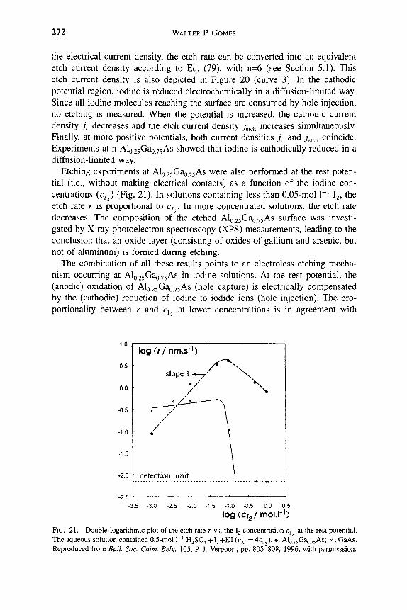
272 WALTER P. GOMES
the electrical current density, the etch rate can be converted into an equivalent etch current density according to Eq. (79), with n=6 (see Section 5.1). This etch current density is also depicted in Figure 20 (curve 3). In the cathodic potential region, iodine is reduced electrochemically in a diffusion-limited way. Since all iodine molecules reaching the surface are consumed by hole injection, no etching is measured. When the potential is increased, the cathodic current density j^ decreases and the etch current density ygt h increases simultaneously. Finally, at more positive potentials, both current densities j^ and j^^^^ coincide. Experiments at U-AIQ 25Gao 75AS showed that iodine is cathodically reduced in a diffusion-limited way.
Etching experiments at Alg 25GaQ 75AS were also performed at the rest poten-tial (i.e., without making electrical contacts) as a function of the iodine con-centrations (cjj (Fig. 21). In solutions containing less than 0.05-mol \~^ I2, the etch rate r is proportional to Cj . In more concentrated solutions, the etch rate decreases. The composition of the etched Alo25Gao75As surface was investi-gated by X-ray photoelectron spectroscopy (XPS) measurements, leading to the conclusion that an oxide layer (consisting of oxides of gallium and arsenic, but not of aluminum) is formed during etching.
The combination of all these results points to an electroless etching mecha-nism occurring at Alo25Gao75As in iodine solutions. At the rest potential, the (anodic) oxidation of AIQ 25Gao 75AS (hole capture) is electrically compensated by the (cathodic) reduction of iodine to iodide ions (hole injection). The pro-portionality between r and q^ at lower concentrations is in agreement with
n.u
0.5
0.0
-0.5
-1.0
-1.5
-2.0
log(r/nm.s'b
slope 1 -^—/
X / '
• detection limit
_i J 1
-3.5 -3.0 -2.5 -2.0 -1.5 -1.0 -0.5 0.0 0.5
logCc/^/mol.I'i)
FIG. 21. Double-logarithmic plot of the etch rate r vs. the I2 concentration q at the rest potential. The aqueous solution contained 0.5-mol T' H2SO4 + I2-I-KI (c^i =4ci ). •, AlojsGaojgAs; x, GaAs. Reproduced from Bull Soc. Chim. Belg. 105, P. J. Verpoort, pp. 805-808, 1996, with permisssion.

6 WET ETCHING OF III-V SEMICONDUCTORS 273
the assumption of an electroless mechanism, since this does not necessitate adsorption of the etchant at the semiconductor surface. That the etching also occurs, although at a lower rate, when an oxide film covers the surface is explained by the ability of holes to tunnel through this film [16].
Similar experiments were performed at p- and n-type GaAs rotating disk elec-trodes. At p-type GaAs, no cathodic reduction current is measured when adding I2 to the indifferent electrolyte solution. This implies that no hole injection occurs, so that an electroless etching mechanism can be excluded. The fact that iodine can inject holes into Alo25GaQ75As but not into GaAs can be explained as follows. The energetic position of the valence band edge is higher at the Alo25Gao75As surface as compared to the GaAs surface (see Fig. 10). Although no reduction current is measured at p-GaAs in contact with iodine solution, GaAs does get etched at open circuit by iodine (Fig. 21). Current-potential dia-grams registered at p-GaAs with and without iodine added show a negative shift in the onset of the anodic dissolution curve (as referred to the flat-band poten-tial). All this is indicative of a chemical etching mechanism. In Figure 21, it is seen that the concentration dependence of the etch rate is less than linear for iodine concentrations below 0.05 mol 1"^ This points to adsorption of iodine at the surface (Freundlich isotherm), in agreement with the fact that interaction between iodine and the GaAs surface is chemical. This difference in concen-tration dependence of the etch rate between Alo 25GaQ 75AS and GaAs leads to inversion of the selectivity at '^ 5 x 10~^-mol 1"' I2.
At both AIQ 25GaQ 75AS and GaAs, the etch rate decreases with increasing q^ in highly concentrated iodine solutions (> 5 x 10"^ mol T^). As can be seen from Figure 21, the decrease is much more drastic for GaAs than for Alo25Gao75As, so that at 0.5-mol 1" I2, the etch rate of GaAs becomes negligible. From the XPS measurements, it was found that oxides are formed during the dissolution of both semiconductors and that the oxide layer thickness d^^ is larger when etching for the same time in solutions in which the iodine concentration is higher. It is reasonable to assume that for both materials, the oxide passivates the surface with respect to etching. The question then arises as to why, although the layer thickness is on the same order of magnitude in both cases, this passivating effect is much more pronounced for GaAs than for Alo25Gao75As. A possible explanation may be offered by the difference in etching mechanism. Electroless etching of AIQ 25Gao 75As implies that holes are injected into the valence band of the semiconductor. Since holes are able to tunnel through an oxide layer, elec-troless etching can still take place when the surface is covered with an oxide. However, the tunneling probability decreases with increasing oxide layer thick-ness. Since d^^ increases with increasing iodine concentration, the decreasing etch rate may be attributed to a smaller tunneling probability. A thickness of ^^3 nm, which is found after etching in 1-mol 1" I2, seems to be a reasonable value for tunneling. In view of the observed high roughness after etching, the oxide layer thickness may be assumed to be highly position dependent. Tunnel-ing may preferentially occur at sites where the layer is thinner. Since the etch

274 WALTER P. GOMES
rate was time independent, the oxide layer thickness is probably controlled by steady-state conditions. In contrast, at GaAs, purely chemical etching by iodine occurs. To react with GaAs surface bonds, I^ ions must adsorb at the surface. The presence of an oxide layer then hinders the contact of the I^ ions with the surface, so that the etch rate may become almost zero when the oxide layer is sufficiently thick, that is, in highly concentrated iodine solutions.
The reason the oxide layer is thicker in solutions with high iodine concentra-tions presumably is connected with the low solubility of the oxidation products in these media. In 1-mol 1" I2, for example, the KI concentration is 4 mol l~^ so that the influence of the decrease in water activity on the solubility of the products must be taken into account.
In the fabrication process of optoelectronic devices, concentrated (= 1 mol r^) iodine solutions are used in = 0.1-mol 1" H3PO4 (pH = 1.6), that is solu-tions in which the pH is higher than in the previously described experiments (pH = 0.3). Therefore, for comparison, in the foregoing fundamental study, etch-ing experiments were also carried out in concentrated I2 + 1 " solutions contain-ing less H2SO4, that is, 0.02 mol T^ (pH = 1.7). At 1-mol 1" I2, the etch rate of AIQ 25Gao75As at pH = 1.7 is, rather surprisingly, found to be about six times higher than at pH = 0.3. The increase in the etch rate of GaAs associated with this increase in pH is even more pronounced, that is, about 2 orders of magni-tude. As a consequence, the selectivity ratio is significantly lower at pH = 1.7 than at pH = 0.3. This initially unexpected decrease in the etch rate caused by increasing the H2SO4 concentration may be explained along the same lines as that caused by increasing the I2 + KI concentration, that is, by considering the effect of the lowering of the water activity on the solubility of the oxidation products.
An alternative mechanism that leads to material-selective etching, that is, galvanic element formation (cathodic protection), can be excluded in the present case. Selective etching of AIQ 25Gao 75 As with respect to GaAs implies that holes are injected into GaAs and consumed in the dissolution of AIQ 25Gao 75 As. Since no holes are injected into GaAs by iodine during etching, this mechanism can be rejected.
Two other examples of material-selective etching pertain to the selective etch-ing of IUQ53Gao47As, lattice-matched on InP, with respect to the InP substrate.
In one case, the etchant was acidic aqueous H2O2 [37]. Hydrogen peroxide does not inject holes into p-InP, so here also, cathodic protection can be ruled out as the origin of the selective etching. At p-type IUQ 53Gao 47 As, hole injection by H2O2 is observed. Under the same circumstances, the semiconductor is also etched, obviously due to a chemical mechanism, since, cathodically, the injected holes are drawn toward the bulk of the sample and hence cannot contribute to etching. Both processes appear to be kinetically controlled. At open circuit, the measured etch rate is approximately the sum of the cathodic rate plus the hole current density converted into an etch rate [see Eq. (79)]. All this shows that at the rest potential, two etching mechanisms operate in parallel, that is, a chemical

6 WET ETCHING OF III-V SEMICONDUCTORS 275
one and an electro-chemical one. As far as InP is concerned, the measured etch rate in H2O2 was very small. Since no hole injection takes place, the mechanism must be chemical. The selective etching is here essentially a consequence of the fact that H2O2 is a very poor etchant for InP, due to the fact that the InP surface is passivated in an oxidizing medium.
In a second case, hexacyanoferrate(III) in an aqueous medium at pH = 14 was tried as a possible selective etchant for Ino53GaQ47As vs. InP [30]. Both sepa-rate semiconductors appear to be etched by Fe(CN)5~, the former at a higher rate than the latter at the same concentration. This can be rationalized on the basis of the relative positions of energy levels. Whereas the valence band edge is located considerably higher for the ternary compound (see Fig. 10), the over-lap with the empty Fe(CN)^~ levels is better. The material-selectivity factor, which is the ratio of the etch rates of Ino53Gao47As vs. InP, was calculated from the data obtained at the separate semiconductors to be around 15 and to be independent of the Fe(CN)^~ concentration. Electrochemical experiments along the lines explained previously helped to establish that the etching mechanism is purely electroless in both cases. With the two semiconductor materials in con-tact (i.e., when etching the multilayer structure), the selectivity factor appeared to reach values over 2000. Apparently a cathodic protection mechanism is oper-ating here. This is not surprising, since hole injection by Fe(CN)^" occurs in both semiconductors and since InP is much more "noble" than Ino53Gao47As (the latter point is again illustrated by the relative positions of the valence band edges of both semiconductors as represented in Fig. 10, which constitutes a rough estimate of their flat-band potentials for p-type samples: V ^ is consider-ably more positive for InP).
7. Etch Morphologies and Profiles
7.1. ETCH MORPHOLOGIES AT MACROSCOPIC SIZE SURFACES
This section on the morphologies that result from wet etching processes at III-V semiconductors starts with a discussion on morphologies obtained at single crystal faces of macroscopic size, that is, obtained by one-dimensional etching. Afterward, the shapes of etch profiles will be considered at the edges of mask grooves, in which case essentially two-dimensional etching is concerned.
7.7.7. (Photo)Electrochemical Etching
The problem of the etch morphology obtained after (photo)anodic etching of III-V compound semiconductors will be discussed primarily on the basis of results obtained on GaP single crystals [69, 96]. The case of strongly alkaline

276 WALTER P. GOMES
( a ) (b)
FIG. 22. Schematic representation of voltammograms for (a) p-type and (b) n-type GaP electrodes in a strongly alkaline aqueous medium.
solutions will be treated first. For the sake of the discussion, the voltammo-grams for p- and n-type electrodes are schematically represented in Figure 22. For p-type GaP (Fig. 22a), distinction has to be made between the exponential region 1 of the j-V curve, in which the current density is determined by the hole-capture rate, and the plateau region 2, in which the anodic current den-sity and hence the etch rate are determined by diffusion of OH" ions toward the surface. For n-GaP (Fig. 22b), distinction has to be made between the pho-tocurrent onset region 1, in which surface recombination of the charge carriers is important, and the photocurrent plateau region, in which the current density is controlled either by 0H~ diffusion (region 2; high light intensities) or by the light-intensity-dependent creation of electron-hole pairs (region 3; low light intensities). The morphological results for the (photo)anodic etching of p- and n-GaP under different circumstances are summarized in Table II.
This table clearly shows that for all three crystal faces studied, etching at a diffusion-limited rate leads to a fiat surface (cases A and E). This is due to the fact that for a diffusion-limited process, the etch rate is the same over the entire surface and is hence unaffected by solid-state factors.
When etching at a rate below the diffusion limit, specific etch patterns develop at the surface due to local differences in the rate of the surface reaction. As a consequence of etching p-GaP in the rising part of the j-V curve (cases B, C, and D), etch pits develop at the surface that have a density of lO^-lO^cm"^ and a geometry depending on the crystal orientation: the pits at the ( lH) and (111) faces exhibit a more or less triangular shape, whereas those at the (100) face are roughly rectangular. Furthermore, it is important to note that at the (111) face, the etch pits are more readily developed than at the ( i l l ) and (100) faces. The etch pit formation and the difference in selectivity are rationalized as

TABLE I1
MORPHOLOGY AFTER (PHOTO)ANODIC ETCHING OF GAP IN AQUEOUS 0.1 MOL L-' KOH
Case ripe Face Etching conditions Rate-determining step Surface morphology
A P (i i i) (1 11) (100)
B P (iii)
Anodic current plateau (Fig. 22a, region 2)
OH- diffusion Smooth
Rising part of j-V curve (Fig. 22a, region 1)
Surface reaction (kinetically controlled)
Triangular etch pits
See D, but more selective
See B See B
See B See B
OH- diffusion
Rectangular pits
Smooth Photocurrent plateau, high light intensity (Fig. 22b, region 2)
Photocurrent plateau, low light intensity (Fig. 22b, region 3)
Hole supply, controlled by e- and h' photogeneration
Microrough
Etch pits See F See F
See F See F Microrough
Photocurrent onset (Fig. 22b, region I)
Hole supply, controlled by e- and h+ photogeneration and recombination
Etch hillocks and ridges

278 WALTER P. GOMES
follows. In a p-type semiconductor, holes are the majority carriers, constituting a quasiequilibrium cloud at the surface. Surface bonds at dislocations and impurity sites may be assumed to be weaker than those at intact sites, resulting in an enhanced hole-capture rate and, hence, in the formation of etch pits at these sites. Assuming that the reactivity at these defect sites is unaffected or hardly affected by the crystal orientation, the observed difference in selectivity can be attributed to differences in the hole-capture rate between the three crystal faces at intact sites, the higher selectivity at the (111) face corresponding to a lower "normal" rate. Remembering that the [111] axis is polar (see Section 4), the difference in the hole-capture rates between the (111) and the ( i l l ) faces can be associated with the GaP surface dipole orientation, which in the case of the ( i l l ) face is in an energetically favorable direction for holes to reach the surface, in contrast to the (HI) face [96]. As to the similar reactivity of the (100) face in comparison to the ( i l l ) face, the assumption is made, based on experimental results, that the etching of the (100) face actually proceeds perpendicularly to the {111} face pairs from the side of the group V element, hence at a rate comparable to that of the ( i l l ) face [69].
When etching n-GaP photoanodically in the onset region 1 of the photocurrent-potential curve (case I), etch hillocks and ridges are observed at the surface after removal of only a small amount of material. In this region of the j-V curve, recombination of the photogenerated charge carriers predominates. As dislocations and damaged sites locally enhance the recombination rate, the local surface concentration of holes will be lower than that of the surroundings, resulting in the formation of etch hillocks. This interpretation of the occurrence of elevations has been evidenced direcdy in the case of n-GaAs anodes by laser scanning of the electrode surface after photoanodic etching, which demonstrated that at elevated lines, apparently associated with mechanical damage, the local photocurrent is indeed lower than elsewhere on the surface [97]. The fact that the etch rate is controlled by the supply of holes, not by their reactivity, explains the similarity in the morphologies obtained at the three faces considered. In the photocurrent plateau region 3, in which the current density is controlled by the light intensity, etching of n-GaP leads either to a large quantity of small etch pits [(111) and (100) face, cases F and H] or to large geometrically shaped etch pits [(111) face, case G]. In contrast to p-GaP, the holes at the n-GaP surface do not necessarily constitute a quasiequilibrium cloud. Instead, they are cre-ated in the semiconductor by light and move through the space-charge region to the surface where they react. Etch pits may then reflect sites of higher reac-tivity and/or be a consequence of an inhomogeneous flow of holes through the space-charge layer [98-100].
In acidic solutions, surface morphologies analogous to the corresponding cases in alkaline solutions are obtained. In contrast to alkaline solutions, how-ever, a steady-state condition in which the anodic current density is diffusion-limited does not exist. Instead, in acidic solutions at sufficiently high anodic current densities, passivation of the GaP surface occurs. Etching in this region

6 WET ETCHING OF III-V SEMICONDUCTORS 279
does not lead to homogeneously flat surfaces; scratches are observed on p-GaP, whereas large-sized etch pits as well as a few scratches form on n-GaP. The development of these etch figures must obviously be related to the physical and chemical properties of the passivation layer, such as the adherence of the layer, the rates of electron and ion transport through this layer, the optical absorption, etc., which are still poorly understood.
Although there are, to our knowledge, no similar systematic studies on the morphology of the (photo)anodically etched surface of GaAs and InP, it seems that several of the conclusions drawn for GaP also hold for these materials. For example, it was found that photoanodic etching of n-GaAs and n-InP in the photocurrent onset region leads to very selective etching and formation of etch hillocks [101, 102], whereas (photo)anodic etching in the (photo)current plateau region of n-GaAs under 0H~ diffusion limitation leads to smooth and structureless surfaces. In the case of InP, diffusion-controlled anodic etching is not feasible due to passivation of the electrode as a result of the formation of an insoluble oxidation product layer involving In(III) compounds [70].
Electrochemical dissolution of n-GaP single crystals under high anodic bias in darkness leads to particular etch morphologies with interesting photoelectro-chemical properties [103, 104]. Indeed, when applying a potential on the order of -HlO V to an n-GaP electrode, the band bending is such that inversion occurs at the semiconductor surface (see Section 2.2) and, hence, the GaP is dissolved by the holes created. The optical and electrical properties of the GaP change dramatically during this anodic dissolution process. The dark anodic current at given potential (+10 V) increases strongly as a function of the charge passed, and the interfacial capacitance at lower anodic potentials, which is a measure of the surface area of the electrode, increases in parallel over more than 2 orders of magnitude. These data suggest that a highly porous structure is formed, a fact that is confirmed by scanning electron microscopy. Pore formation is apparently initiated by preferential attack, probably through avalanche breakdown at a small number of localized sites on the surface such as dislocations, and from these initial pores, a radial system of pores with structural details in the 50-200-nm range develops. These microporous electrodes appear to exhibit a quantum effi-ciency for bandgap (green) light close to unity, in contrast to a value near 0.01 for nonporous GaP. This effect can be ascribed to two reasons: enhanced light scattering that gives rise to a more effective absorption of photons in the porous layer and the fact that even at a considerable depth, the photogenerated holes have to travel only over a short distance to reach the semiconductor-electrolyte interface. Subbandgap photocurrents also have been observed [105]. These results are clearly important for improving the photoresponse of junc-tions based on semiconductors in which the light absorption coefficient and the diffusion length of minority carriers are small. Pore formation in GaAs has also been reported, but was less extensively studied [106].

280 WALTER R GOMES
7.1.2. Photoetching
Photoetching has been reported to lead to etch hillocks (see, e.g., [12, 107]). This can be explained as follows. As mentioned previously, the rest potential is generally situated in the onset region of the photocurrent curve, where a considerable fraction of the photogenerated minority carriers are consumed in surface recombination. The latter process is favored at surface defects, so that the reaction rate and hence the etching is lower at defect sites. Photoetching can thus be used for defect-revealing purposes.
An interesting case is that of the photoetching of GaAs by H2O2 [12]; see also Section 5.2. The formation of the surface precursor at n-GaAs is kineti-cally controlled. In the dark, this reaction is followed by chemical etching, by which a rough surface is obtained. Under illumination, photoetching takes place. Whereas the etch rate is controlled by the formation rate of the precursor, it is the same for photoetching as for dark etching. Nevertheless, under illumination, the resulting etch morphology is entirely different: lattice defects are clearly revealed as etch hillocks.
The situation may, however, be more complex, such as in the case of the pho-toetching of GaP by hypobromite [96] (see also Section 5.2). Photoetched (111) and ( i l l ) faces of GaP in alkaUne OBr" solutions show a remarkable difference in morphology depending on the type of semiconductivity: etch hillocks develop on n-GaP, whereas etch pits are formed on p-GaP. To explain these facts, it is assumed that on the microscale, the two partial reactions under consideration do not necessarily take place at the same sites. The morphology thus reflects local differences in the hole supply rate for n-GaP and local differences in the hole-capture reactivity for p-GaP. At n-GaP, the anodic partial reaction proceeds by the minority carriers. Whereas at the rest potential, recombination processes determine the availability of holes and hence the value of the current density, the hillocks formed by photoetching correspond to sites where the recombina-tion rate is high (dislocation sites, damaged areas). In the case of p-GaP, how-ever, where the holes are the majority carriers, locally enhanced recombination leads to a local decrease of the cathodic partial current density (and hence to a decrease of the overall etch rate), but does not significantly influence the local anodic partial current density. Here, however, the holes are at quasiequilibrium at the surface, so etch pits develop at sites with an enhanced reactivity for hole-capture.
In contrast, in the case of GaAs photoetching in CrOj-HF solutions, etch hillocks are formed both on n- and p-type samples [107, 108]. Hillocks are also observed when etching in darkness, and their occurrence has been explained on the basis of a complex reaction scheme. The Cr03-HF photoetch has been found to be very sensitive to defects at GaAs and even more so at InP crystals [109].
Another fact that demonstrates the complexity of the phenomena that control the photoetch morphologies is that, in contrast to the cases mentioned previ-ously, photoetching of n-InP in Fe^"^-containing aqueous HCl solutions leads to

6 WET ETCHING OF III-V SEMICONDUCTORS 281
etch pits [56]. Obviously, the structural defects that determine the etch morphol-ogy must be entirely different in the latter case.
7.1.3. Electroless Etching
Similarly as for the kinetics and mechanisms of electroless etching (Section 5.3), the GaP-Fe(CN)^" system will be used to illustrate the factors that determine the macroscopic morphology in electroless etching. Alkaline K3Fe(CN)6 solutions are often used to differentiate between the two polar faces of GaP, that is, the (111) and ( i l l ) faces [110]. In fact, in most cases triangular etch pits develop at the (111) face, whereas the ( i l l ) face is etched homoge-neously. The situation, however, is slightly more complex, since triangular etch pits were also observed at ( i l l ) p-GaP, but only at Fe(CN)^~ concentrations below 0.3 mol T^ and after a very long etching time. For the purpose of the dis-cussion of these observations, the morphological results on electroless etching by Fe(CN)^~ are summarized in Table III.
The morphology of etched surfaces can be rationalized on the basis of the electroless mechanism and hence of electrochemical principles. It is thereby assumed that the two partial electrochemical reactions that constitute the elec-troless process do not necessarily take place at the same sites. Furthermore, since only the anodic partial current involves dissolution of the semiconductor, it is important to realize that the surface morphology reflects only local differ-ences in the anodic partial current density. In p-GaP, the holes, which are the majority carriers, are at quasiequilibrium at the surface. The anodic partial reac-tion rate at a given site is thus determined by the local hole-capture reactivity, which hence determines the surface morphology, except when the anodic partial reaction rate is limited by OH" diffusion: in the latter case, the rate is the same
TABLE m
MORPHOLOGY AFTER ELECTROLESS ETCHING OF GAP IN FE(CN)^~ SOLUTIONS (PH = 13)
Face
(111)
(iii)
(iii) (Ili) (iii)
Type
p, n
P
P
n
n
Fe(CN)^ concentration
(mol. 1-')
c<\
c < 0 . 3
0.3 < c < 1
c < 0 . 3
0 . 3 < c < 1
Rate-determining step
Injection of h+, kinetically controlled
Fe(CN)^- diffusion
0H~ diffusion
Fe(CN)3- diffusion
OH" diffusion
Morphology
Triangular pits
Triangular pits after long etching time
Smooth
Smooth
Smooth
282 WALTER P. GOMES
over the entire surface. The case of n-GaP is quite different. Here, holes are the minority carriers, and since they can be assumed to be very rapidly captured in surface bonds, it is now the availability of holes at the surface that determines the anodic partial reaction rate and hence the surface morphology. In electroless etching, holes are supplied by injection from solution, so that for n-GaP, the anodic partial reaction is expected to take place near the sites where the holes are injected by Fe(CN)5". The morphology hence reflects local differences in the hole-injection rate. If either the injection rate is limited by Fe(CN)6" diffu-sion or the anodic partial reaction rate is limited by OH" diffusion, the anodic partial current density is the same over the entire surface.
Keeping these principles in mind, the interpretation of the morphology data in Table III is straightforward. At the (111) face, the overall etch rate is kinetically controlled. The j-V curves for the p-type (111) GaP face are schematically shown in Figure 8a (omitting the potential dependence of the hole-injection rate), which demonstrates that the situation at the rest potential V corresponds to the rising part of the anodic partial current density. Etch pits are formed due to local differences in hole-capture reactivity, analogously to the anodic etching of p-GaP in the rising part of the j-V curve (see Table II, case C). The j-V behavior of the n-type (111) GaP face is schematically represented in Figure 8b. Etch pits are formed at sites with a locally higher hole-injection rate, due to a locally higher position of the valence band edge (dislocation sites). In this case, the situation is analogous to the photoanodic etching of n-GaP in the photocurrent plateau (Table II, case G) in that the morphology is determinedby local differences in the availability of holes at the surface. For the p-type ( i l l ) GaP face and at low Fe(CN)^~ concentrations (<0.3 mol T^), the overall etch rate is determined by diffusion of Fe(CN)5~. The rest potential V is thus located in the rising part of the anodic partial current density curve, and etch pits are similarly formed as a result of local differences in the hole-capture reactivity. The fact that these pits are only visible after a long etching time may be ascribed either to the low etch rate at these low concentrations or, alternatively, to the low selectivity of the ( i l l ) face, as discussed in Section 7.3.1. At high Fe(CN)^" concentrations, the overall etch rate at p-GaP is determined by the diffusion rate of 0H~. The rest potential V thus corresponds to the diffusion-limited plateau region of the anodic partial current density curve, so that etching leads to a homogeneously flat surface, as in the case of anodic etching of p-GaP in the diffusion-limited regime (Table II, case A). For the n-type ( i l l ) GaP face at low Fe(CN)^~ concentrations (<0.3 mol 1~ ), the overall etch rate is determined by Fe(CN)^~ diffusion. The etched surface is homogeneously flat, since the hole supply, that is, the hole-injection rate, is the same all over the surface. At high Fe(CN)^~ concentrations (>0.3 mol T^), the overall etch rate at n-type (111) GaP is limited by 0H~ diffusion. A flat surface is obtained, analogously to the diffusion-limited, photoanodically etched surface.
In summary, the interpretation of the morphology of electroless etching pro-cesses at GaP is analogous to the proposed interpretation of (photo)anodic etch-ing. In electroless etching, however, the potential is not applied by an external

6 WET ETCHING OF III-V SEMICONDUCTORS 283
source, but it is imposed as a rest potential through addition of Fe(CN)^~ to the solution.
In the case of open-circuit etching of GaAs in K3Fe(CN)6 solutions, it was found that etch pits develop at both n- and p-GaAs when etching is diffusion-limited through the cathodic partial reaction [12]. The fact that with GaAs, in contrast to GaP, a distinction between diffusion limitation by the cathodic and by the anodic partial reactions is also observed at n-type crystals may be due to the higher hole mobility in GaAs, which might enable the holes, injected at a diffusion-limited rate, to move along the surface before being captured selectively.
7.1.4. Chemical Etching
In chemical etching of III-V compound semiconductors, differences in the etch morphology that depend on the crystal face have been reported. For exam-ple, a homogeneously flat ( i l l ) surface is obtained, whereas triangular etch pits are formed on the (111) face in the case of GaP-aqueous Br2 [49], GaP-methanolic Br2 [74], and InP-HI03 [^l]- These chemical etchants hence can be used to differentiate between the two surfaces perpendicular to the [111] axis. Considerations involving free charge carriers are evidently irrelevant in the interpretation of these differences. Rather, one should consider that in all these cases, the etch rate at the ( i l l ) face is diffusion-controlled and hence equal at all sites, whereas the etch rate at the (111) face is limited by the surface reaction itself, the rate of which is locally higher at defect sites. The triangular shape of the pits evidently reflects the symmetry of the (111) face. Interpretations for the difference in kinetics were presented in Section 5.4.
The interpretation of the morphology of chemical etching is not always that simple, however. A more complicated case, for example, is the etching of InP by HIO3 [51]. In this case, it was found that although the etch rate is diffusion-controlled at all three crystal faces investigated [(HI), ( i l l ) , and (100)], tri-angular etch pits develop at the (111) face, whereas the ( i l l ) and (100) faces are etched more or less homogeneously. The following explanation has been proposed. The etching mechanism consists of different consecutive steps that involve the formation of decomposition intermediates and of intermediates of the HIO3 reduction. The rate of the first step in the etching reaction, in which an In—P bond is broken by an HIO3 molecule (leading to the formation of a first intermediate X^), may be assumed to be determined by the supply of HIO3 at the surface. Hence, at all surface sites, X^ is formed at the same rate. If, however, one of the subsequent steps is sensitive to local variations in the reac-tion rate, then the reaction between an intermediate of the HIO3 reduction and a decomposition intermediate will be slow at sites with a low intrinsic reaction rate, so that intermediates will be able to move along the surface and hence to react selectively at sites with a higher intrinsic rate. At these sites, etch pits

284 WALTER P. GOMES
develop. The fact that no pits are observed at the ( i l l ) and (100) faces can be explained by assuming a higher reactivity at these faces, analogously to the etching of GaP, so that at these faces, the intermediates are less likely to move along the surface.
7.2. PROFILE ETCHING
7.2.7. General
In the processing of semiconductors for electronic and optoelectronic device technology, often small parts of a semiconductor sample or layer have to be removed according to well-defined patterns. This selective removal is mostly performed by covering the remainder of the surface with a masking layer that prevents the attack of the semiconductor surface by the wet etchant. The mask may consist either of a photoresist layer or of a dielectric layer (e.g., siHcon dioxide or silicon nitride), deposited by techniques such as plasma-enhanced chemical vapor deposition. It is obvious that the etching procedures must meet very specific requirements, depending on the application. A factor of consid-erable importance is the shape of the etching profiles near the mask edges. Whereas profiles etched near mask edges are usually of micrometer scale size, this type of etching is denoted as microscopic etching. To discuss this type of etching problem, a two- or a three-dimensional approach is necessary. Since the semiconductor material covered by the mask is monocrystalline, the micro-scopic etching kinetics of all crystallographic planes, in principle, has to be considered near the mask edge; in practice, this is hardly feasible. With III-V compounds that have the zincblende structure, the fact has to be taken into account that a polar face consisting of group III atoms exclusively usually has a much lower etch rate than a polar face consisting of group V atoms. It has been shown from many experimental data that the etching kinetics plays a decisive role in the determination of the profile shape and that the macroscopic etching kinetics of various crystallographic planes constitutes, in many cases, a good guideline for predicting the microscopic profile shape. With etchants operat-ing through a chemical mechanism, certain crystallographic facets are revealed when the dissolution rate of all crystallographic planes is controlled by the sur-face reaction. However, when the rate of the surface reaction is very high for all faces, then two-dimensional mass transport of etching species becomes rate-determining, generally resulting in rounded profiles. Intermediate profiles, the shapes of which are partly determined by the kinetics of the surface reaction and partly by mass transport, are also found. Although similar rules as for chemical etching hold for etching according to an electroless mechanism, complications may arise in the latter case (see Section 7.2.4.). We now illustrate the preceding principles with some examples.

6 WET ETCHING OF III-V SEMICONDUCTORS 285
72.2. Diffusion-Controlled Etching Profiles
When the etching reaction is controlled by diffusion from solution, a con-centration gradient of the etchant builds up at the semiconductor-liquid inter-face. At a macroscopic surface, one-dimensional diffusion has to be considered. Therefore, the concentration gradient and hence the etch rate is independent of the position at the semiconductor surface. However, in the case of mask etch-ing, two-dimensional diffusion of the etchant has to be taken into account in the neighborhood of the mask edges, so that the concentration gradient depends on the position at the surface. To predict the shape of etch profiles near mask edges, the concentration gradient should, therefore, be calculated as a function of both the etch time and the position with respect to the mask edges. The-oretical models have been developed on this basis [111-114]. Two cases can be distinguished, depending on whether the mask can be considered as "semi-infinite" or is characterized by slits that are so narrow that their width affects the profile shape. As an example. Figure 23 shows experimental and calculated results on the profiles obtained with (100) GaAs in a diffusion-controlled etchant for the face mentioned [H202-concentrated aqueous HCl (1:40)] [12]. A Si02 layer aligned in the [110] direction masked half of the sample (semi-infinite mask). Comparison of the experimental and calculated profiles shows that the theory accounts very well for the various features of the profile, including the rounded shape, the underetching of the mask, and the bulge in the profile. No trace of any facet is observed in the scanning electron microscope (SEM) pho-tograph, indicating that not only the (100) face, but also all other crystal planes are etched under diffusion limitation.
7.2.3. Kinetically Controlled Etching Profiles
In the case of kinetic control, the macroscopic etching kinetics of the various crystal planes has to be considered to understand and predict the shape of pro-files near mask edges. The kinetics of the slowest etching faces is expected to determine the shape of these profiles. In principle, the prediction is anticipated to hold for etching through a chemical as well as through an electroless or a photoetch mechanism. As an example, we consider the case of the photoetch-ing of (100) InP in Fe^"^-containing aqueous HCl [56]. To perform the profile etching experiments, the (100) surface was covered by a dielectric mask, where the mask patterns consisted of squares (1.2-mm size) with the sides oriented along the [Oil] and [Oil] axes (see Fig. 24). These directions are perpendicu-lar to the two faces that can be obtained easily by cleavage, that is, the (Oil) and (Oil) faces, respectively. The slit width between the squares was 300 |Lim. The semiconductor was etched for 1 h under uniform illumination. Figure 25 shows typical examples of etched profiles obtained at p-type InP. For the mask edge oriented in the [Oil] direction, a facet is clearly revealed near the edge.

286 WALTER P. GOMES
A.
B. \ sdutiml
f- 'N^ mask J
solid c. FIG. 23. (A) SEM photograph of a profile etched in GaAs with a semi-infinite Si02 mask aligned in the [110] direction. Etching was carried out for 5 min in a HjOj-HCl (1:40) solution with the wafer placed in a vertical position. (B) A higher magnification of the same profile in the mask edge region. (C) The agreement between the profile measured in (B) (continuous line) and that calculated from theory (filled circles). The underetching and the maximum etched depth are indicated by XQ and Yf,, respectively. Reprinted from P. H. L. Notten, J. E. A. M. van den Meerakker, and J. J. Kelly, "Etching of III-V Semiconductors: An Electrochemical Approach," ©1991, with permission from Elsevier Science.
making an angle of 55° with the (100) surface (see Fig. 25a). Hence, it can be attributed to the (111) In face [115]. As can be seen, the bottom of the etched groove is flat. A typical example of a profile obtained in the [Oil] direction is shown in Figure 25b. Again a facet is revealed, in this case making an angle of about 125° with the (100) surface, so that the etch groove has a so-called dove-tail shape. From crystallographic considerations, it can be concluded that again the (111) In face is involved [115]. Although a small curvature is observed near the mask edge, the bottom of the groove is flat in the middle.
As mentioned in Section 5.2, the photoetch rate of the (111) InP face in Fe^+ is relatively low, which accounts for the facets developed and, hence, for the shapes of the etch profiles. In the case of photoetched n-InP with the mask edge

6 W E T ETCHING OF I I I - V SEMICONDUCTORS 287
[011]
(Oil)
FIG. 24. Schematic representation of a masking pattern on the (100) InP surface. The mask edges are aligned either in the [Oil] or the [Oil] direction. Reprinted from J. Electrochem. Soc. 142,1. E. Vermeir, W. P. Gomes, and P. Van Daele, pp. 3226-3232, 1995. Reproduced by permission of The Electrochemical Society, Inc.
•;iif»:::
20 pm
(a)
InP
20vm
(b)
FIG. 25. Photographs of profiles obtained at a silicon nitride mask on (100) p-InP after 1-h etching under illumination in 2-mol 1' FeCl3 H-HCl (pH = 0); (a) aligned in the [Oli] direction; (b) aligned in the [Oil] direction. Reprinted from 7. Electrochem. Soc. 142, I. E. Vermeir, W. P. Gomes, and R Van Daele, pp. 3226-3232, 1995. Reproduced by permission of The Electrochemical Society, Inc.

288 WALTER P. GOMES
oriented along the [Oil] direction, the sidewall also makes an angle of about 55° with the (100) face. Here, however, complications arise due to the fact that the bottom of the groove shows a very rough structure. For a discussion on this problem, refer to [56].
It should be mentioned that whereas usually the (100) face of III-V semi-conductors is used for mask etching and usually the (111) face is the slowest etching face under kinetic control, sidewalls with inclinations as shown are very common.
7.2A. Complications Due to Cathodic Protection of Crystal Faces
As mentioned before, when all crystal planes are etched at a diffusion-limited rate, rounded profiles at mask edges are normally expected. This is certainly the case when the etching mechanism is chemical. In the case of electroless etch-ing, however, exceptions with respect to this rule have been observed, namely in cases in which the diffusion-limiting step is the cathodic (hole-injection) reac-tion. In the electroless etching of n-GaAs in 0.1-mol 1" Fe(CN)^~ solution at pH = 13, for example, in which diffusion of the Fe(CN)^" is the rate-limiting step, the (111) face is clearly revealed near the mask edge [12]. In the same solution but at 0.5-mol T^ Fe(CN)^", however, in which the rate-Hmiting step is not diffusion of Fe(CN)^" but that of 0H~ ions, a rounded profile is observed. These findings can be rationalized along the same lines as those developed to explain certain material-selectivity phenomena (see Section 6), that is, on the basis of a cathodic protection model. Indeed, as mentioned before, the flat-band potential of a given semiconductor in a solution of given composition may be different for different crystal faces exposed to the electrolyte, due to differences in the structure of the Helmholtz layer. In the case of GaAs, the (111) face appears to have a flat-band potential that is about 200 mV more positive than that of the (111) and (100) faces (cf. Section 5.3). Taking the case of p-GaAs, this implies that at the same electrode potential, the equilibrium hole concen-tration at the surface p^ is lower at the (111) face than at the ( i l l ) and (100) faces. Experimentally, this is reflected by the relative positions of the anodic dissolution curves in the sense that the onset is more positive for the (111) face. The observed effect can then be explained on the basis of the same figure as that used for explaining material selectivity by cathodic protection (Section 6, Fig. 19), but with the left and the right curves representing, in the present case, that for the ( i l l ) and for the (111) faces of GaAs, respectively.
When a single crystal is etched at a mask edge, various crystal planes are exposed to the solution, so that the possibility of local element formation between crystallographic faces must be envisioned. Considering Figure 19, it is clear that although the etch rate at all separated faces is controlled by diffusion of the hole-injection agent, with both faces in contact with the solution and in mutual electrical contact, the etch rate of the "more noble" face [the (111) face]

6 WET ETCHING OF III-V SEMICONDUCTORS 289
will be diminished and that of the "less noble" face [the ( i l l ) face] will be enhanced. As a consequence, although hole injection at the mask edge takes place at a diffusion-limited rate over the entire semiconductor surface, part of the holes injected at the (111) areas will be transported through the semiconduc-tor to a neighboring less noble area, where they will cause anodic dissolution. This will result in "cathodic protection" of the (111) face; that is, this face will dissolve at a relatively low kinetically controlled rate, so that a (111) facet will develop.
72,5. Complications Due to Native Oxide Layers
In the foregoing paragraph, a faceted profile was observed, although a rounded profile would be anticipated. The inverse effect appears to exist also. This point will be exemplified by the InP-HIOg system [56]. In the experiments that follow, the configuration is again that of Figure 24. Profile etching experiments were performed in aqueous 10~^-mol 1" KIO3 -f HCl (pH = 0) in darkness. Photore-sist as well as silicon nitride masks were used. The samples were etched for 30 min. Figure 26 shows examples of etched profiles obtained at p-type samples covered with a photoresist mask. The profile obtained for the photoresist mask edge in the [Oil] direction does not reveal any crystallographic facet; instead, a rounded profile is observed (Fig. 26a). For the mask edge oriented in the [Oil] direction, however, a faceted structure is observed (Fig. 26b). The facet makes an angle of about 47° with the (100) face, which implies that either a (221) or a (331) face is involved [116]. These faces are stepped faces that consist of In atoms and can be considered as combinations of (111) and (110) planes [117].
In view of the discussion in the next section, a top view of an etched p-type sample covered with a photoresist mask is shown in Figure 27. The broad white fringe observed at the mask edge in the [Oil] direction indicates that the underetching is much more important at this edge than at the resist edge oriented in the [Oil] direction. The same results were obtained at n-type samples.
For the sake of the discussion, it is important to realize that HIO3 etches InP through a chemical mechanism and that the macroscopic etch rate at the (100), (111), and (111) faces of InP under the given circumstances is diffusion-controlled [51]. If the same were true for any other face, rounded profiles would be expected, as indeed observed when the mask edge is oriented in the [Oil] direction. However, with the mask edge oriented in the [Oil] direction, a facet [either (221) or (331)] is developed, suggesting that the face concerned is etched slowly. Confirmation of this assumption by etching of a (221) or a (331) single crystal face was not possible, since no samples with the given orientation were available. It is important to note that an alternative mechanism that leads to facet development (i.e. galvanic cell formation) can be excluded because the etching mechanism is chemical.

290 WALTER R GOMES
. 20Mm ,
(a)
20 Mm
(b)
FIG. 26. Photographs of profiles obtained at (100) p-InP covered with a photoresist mask after 30-min etching in lO'^-mol 1" KIO3 + HCI (pH = 0): (a) mask aligned in the [Oil] direction; (b) mask aligned in the [Oil] direction. Reprinted from J. Electrochem. Soc. 142, I. E. Vermeir, W. P. Gomes, and P. Van Daele, pp. 3226-3232, 1995, Reproduced by permission of The Electrochemical Society, Inc.
The question now arises why, in contrast to the photoetching in FeClg, the "slow" face is not revealed when the mask edge is oriented in the [Oil] direc-tion. Notten [118] observed an analogous anisotropy in profile shape when etch-ing InP in Br2 + HBr and proposed an interpretation for this anisotropy.
It is assumed that on top of the InP sample (i.e., between the InP and the mask), a thin oxide film is present and that an anisotropy exists in the lateral dissolution rate of this film. The anisotropy exists in the sense that the lateral etch rate is high at the mask edge oriented in the [Oil] direction but low at the mask edge oriented in the [Oil] direction. This anisotropy is demonstrated experimentally by the pronounced underetching of the [01 ij oriented mask edge, in contrast to the less pronounced underetching of the [011] oriented edge after etching in HIO3 solution (see top view in Fig. 27). This anisotropy suggests that the oxide film has an ordered structure.
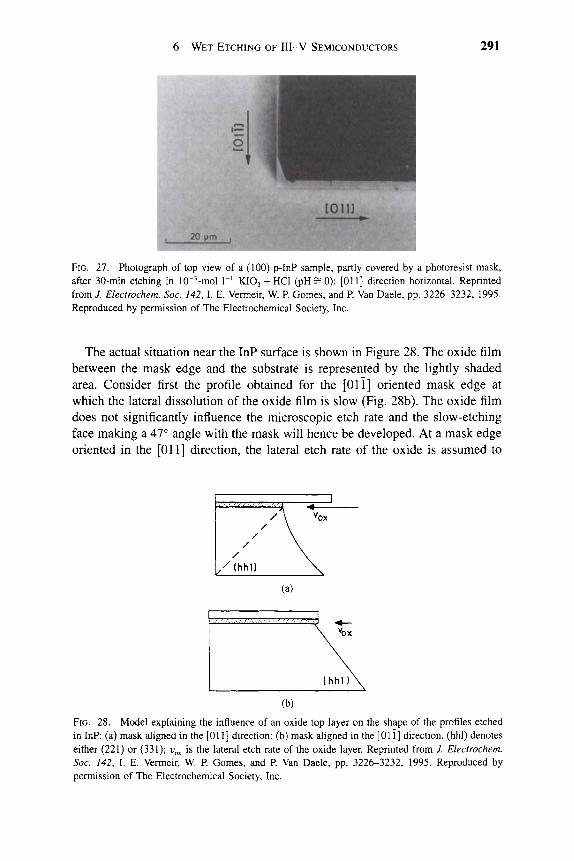
6 WET ETCHING OF III-V SEMICONDUCTORS 291
FIG. 27. Photograph of top view of a (100) p-InP sample, partly covered by a photoresist mask, after 30-min etching in lO'^-mol T^ KIO3 + HCI (pH = 0): [Oil] direction horizontal. Reprinted from J. Electrochem. Soc. 142,1. E. Vermeir, W. P. Gomes, and P Van Daele, pp. 3226-3232, 1995. Reproduced by permission of The Electrochemical Society, Inc.
The actual situation near the InP surface is shown in Figure 28. The oxide film between the mask edge and the substrate is represented by the lightly shaded area. Consider first the profile obtained for the [Oil] oriented mask edge at which the lateral dissolution of the oxide film is slow (Fig. 28b). The oxide film does not significantly influence the microscopic etch rate and the slow-etching face making a 47° angle with the mask will hence be developed. At a mask edge oriented in the [Oil] direction, the lateral etch rate of the oxide is assumed to
(a)
(b)
FIG. 28. Model explaining the influence of an oxide top layer on the shape of the profiles etched in InP: (a) mask aligned in the [Oil] direction; (b) mask aligned in the [Oil] direction, (hhl) denotes either (221) or (331); v^^ is the lateral etch rate of the oxide layer. Reprinted from /. Electrochem. Soc. 142, I. E. Vermeir, W. R Gomes, and R Van Daele, pp. 3226-3232, 1995. Reproduced by permission of The Electrochemical Society, Inc.

292 WALTER P. GOMES
be diffusion-limited. In that case, the slow-etching face would then be expected to appear, extending from the oxide edge into the substrate, as symbolized by the dashed line in Figure 28a. This face is, however, not developed: since the lateral etch rate of the oxide is diffusion-limited, the top layer of the InP itself is in direct contact with the etching solution. The etch rate of this (100) face is diffusion-Hmited as well. Consequently, a rounded profile will be obtained.
When photoetching InP in FeCl3 -f HCl, one may wonder why, in contrast to the dark etching by KIO3 -hHCl, a dovetail profile at the [Oil] oriented mask edge is developed, even though the properties of the oxide film and the pH of the solution attacking this oxide are the same in both cases. The crucial point is evidently that in HIO3, the etching of the (100) face is diffusion-limited, whereas in FeCl3, it is not.
8. Conclusions
From the preceding discussion, it appears that the strategy of combining electrochemical and etch rate measurements constitutes a powerful tool for unraveling the mechanisms of etching reactions at III-V semiconductors, so considerable mechanistic information on these reactions is currently available. Insight into the mechanisms of wet etching reactions provides a fundamental scientific basis for controlling etch rates and for development of new etching procedures, which in the past were established mainly by trial-and-error. This scientific approach is essential in view of the ever-increasing complexity and degree of miniaturization in device fabrication. Understanding and controlling etch rates is particularly important in cases where material-selective etching is involved, as is often the case with III-V multilayer structures used for opto-electronic device fabrication. Insight into the rates and mechanisms of etching reactions at III-V semiconductors also appears to lead to a better understanding of macroscopic and microscopic etch morphologies. Even more detailed (i.e., atomic scale) information on etching mechanisms and on the origin of etch mor-phologies may be expected in the near future as a result of in situ surface studies during etching reactions by surface spectroscopic techniques and by scanning tunneling microscopy. In the case of GaAs, promising results reported recently were obtained from the in situ use of these experimental methods in the course of various electrochemical reactions [119, 120, 121].
ACKNOWLEDGMENT
Most of the work performed by the author and his co-workers and cited in the text was performed in the framework of a Gemeenschappelijk Overlegde Actie program, financed by the Ministry of the Flemish Community (Ministerie van de Vlaamse Gemeenschap), Belgium.
6 WET ETCHING OF I I I - V SEMICONDUCTORS 293
References
1. G. E. Thomas, Philips Tech. Rev. 44, 51 (1988). 2. C. E. Timmerig, J. M. Langemaat, C. T. Foxon, and J. J. Harris, Semicond. Sci. Technol. 3,
1139(1988). 3. E A. Ponce and D. P. Hour, Nature 386, 351 (1997). 4. S. Nakamura, Science 281, 956 (1998). 5. A. Kautek, S. K. Krawczyk, and R. Olier, J. Electrochem. Soc. 134, 1859 (1987). 6. J. L. Weyher and J. van de Ven, J. Cryst. Growth 78, 191 (1986). 7. R. R Tijburg and T. van Dongen, J. Electrochem. Soc. 123, 687 (1967). 8. H. Gerischer, Ber Bunsen-Ges. Phys. Chem. 69, 578 (1965). 9. H. Gerischer and I. Mattes, Z Phys. Chem. NF 49, 112 (1966).
10. H. Gerischer and I. Willem-Mattes, Z Phys. Chem. NF 64, 187 (1969). 11. H. Gerischer, Surf. Sci. 18, 97 (1969). 12. P H. L. Notten, J. E. A. M. van den Meerakker, and J. J. Kelly, "Etching of III-V Semicon-
ductors: An Electrochemical Approach." Elsevier Advanced Technology, Oxford, 1991. 13. W. P. Gomes and H. H. Goossens, in "Advances in Electrochemical Science and Engineering"
(H. Gerischer and C. W. Tobias, Eds.), Vol. 3, Chap. 1. VCH, Weinheim, 1994. 14. H. Gerischer, in "Advances in Electrochemistry and Electrochemical Engineering" (P. Delahay,
Ed.), Vol. 1, p. 139. Interscience, New York, 1961. 15. H. Gerischer, in "Physical Chemistry, An Advanced Treatise" (H. Eyring, Ed.), Vol. IX A,
p. 436. Academic Press, New York, 1970. 16. S. R. Morrison, "Electrochemistry at Semiconductor and Oxidized Metal Electrodes." Plenum,
New York, 1980. 17. Yu. V. Pleskov and Yu. Ya. Gurevich, "Semiconductor Photoelectrochemistry." Consultants
Bureau, New York, 1986. 18. Z. Hens and W. P Gomes, Phys. Chem. Chem. Phys. 1, 3607 (1999). 19. H. Gerischer and W. Mindt, Electrochim. Acta 13, 1329 (1968). 20. L. M. Peter, J. Li, and R. Peat, Electrochim. Acta 35, 1657 (1990). 21. L. M. Peter, A. M. Borazio, H. J. Lewerenz, and J. Stumper, J. Electroanal. Chem. 290, 229
(1990). 22. W. J. Albery and M. L. Hitchmann, "Ring-Disc Electrodes." Clarendon, Oxford, 1971. 23. Yu. V. Pleskov and V. Yu. Filinovskii, "The Rotating Disc Electrode." Consultants Bureau,
New York, 1976. 24. S. R. Morrison and T. Freund, J. Chem. Phys. 47, 1543 (1967). 25. W. P Gomes, T. Freund, and S. R. Morrison, J. Electrochem. Soc. 115, 818 (1968). 26. R. Memming, J. Electrochem. Soc. 116, 785 (1969). 27. W. P Gomes and E Cardon, Prog. Surf. Sci. 12, 155 (1982). 28. A.-M. Van Wezemael, W. H. Laflere, E Cardon, and W. P Gomes, J. Electroanal. Chem. 87,
105 (1978). 29. Ph. Verpoort, Ph.D. Thesis, University of Ghent, 1997. 30. A. Theuwis, Ph.D. Thesis, University of Ghent, 1998. 31. I. M. Huygens, K. Strubbe, and W. P Gomes, J. Electrochem. Soc. 147, 1797 (2000). 32. R. L. Meek and N. E. Schumacher, J. Electrochem. Soc. 119, 1148 (1972). 33. M. J. Madou, F. Cardon, and W. P Gomes, Ben Bunsen Ges. Phys. Chem. 81, 1186 (1977). 34. P A. Kohl, C. Wolowodiuk, and F W. Ostermayer Jr., J. Electrochem. Soc. 130, 2288 (1983). 35. S. Preusser, M. Herlem, A. Etcheberry, and J. Jaume, Electrochim. Acta 37, 289 (1992). 36. P J. Verpoort, I. E. Vermeir, and W. P Gomes, J. Electrochem. Soc. 142, 3589 (1995). 37. A. Theuwis and W. P Gomes, J. Electrochem. Soc. 144, 1390 (1997). 38. R. Memming and G. Schwandt, Electrochim. Acta 13, 1299 (1968). 39. C. Yontsey, I. Adesida, and G. Bulman, Appl. Phys. Lett. 71, 2151 (1997). 40. J. Van de Langemaat, Ph.D. Thesis, University of Utrecht, 1998. 41. M. Pourbaix, "Atlas d'Equilibres Electrochimiques," p. 436. Gauthier-Villars, Paris, 1963.
294 WALTER P. GOMES
42. T. Solomun, R. Mclntyre, W. Richtering, and H. Gerischer, Surf. ScL 169, 414 (1986). 43. S. Lingier and W. R Gomes, Ber. Bunsen Ges. Phys. Chem. 95, 170 (1991). 44. F. Decker, Electrochim. Acta 30, 301 (1985). 45. D. Vanmaekelbergh, J. J. Kelly, S. Lingier, and W. R Gomes, Ber. Bunsen Ges. Phys. Chem.
92, 1068 (1988). 46. D. Vanmaekelbergh and J. J. Kelly, J. Electrochem. Soc. 136, 108 (1989). 47. B. H. Erne, D. Vanmaekelbergh, and I. E. Vermeir, Electrochim. Acta 38, 2559 (1993). 48. A. Theuwis, I. E. Vermeir, and W. R Gomes, / Electroanal. Chem. 410, 31 (1996). 49. H. H. Goossens, K. Strubbe, and W. R Gomes, J. Electroanal. Chem. 286, 133 (1990). 50. K. Strubbe and W. R Gomes, J. Electrochem. Soc. 140, 3301 (1993). 51. I. E. Vermeir, H. H. Goossens, F. Vanden Kerchove, and W. P. Gomes, J. Electrochem. Soc.
139, 1389 (1992). 52. H. Gerischer, J. Electroanal. Chem. 58, 263 (1975). 53. D. Vanmaekelbergh and W. R Gomes, J. Phys. Chem. 94, 157 (1990). 54. D. Vanmaekelbergh, C. W. Hoogendam, and J. J. Kelly, J. Electroanal. Chem. 270, 175 (1989). 55. I. E. Vermeir, F Vanden Kerchove, and W. R Gomes, J. Electroanal. Chem. 313, 141 (1991). 56. I. E. Vermeir, W. R Gomes, and R Van Daele, J. Electrochem. Soc. 142, 3226 (1995). 57. H. H. Goossens, F Vanden Kerchove, and W. R Gomes, J. Electroanal. Chem. 261, 89 (1989). 58. H. H. Goossens, W. R Gomes, and F Cardon, J. Electroanal. Chem. 278, 335 (1990). 59. J. J. Kelly, J. E. A. M. van den Meerakker, R H. L. Notten, and R. R Tijburg, Philips Tech.
Rev. 44, 61 (1988). 60. B. R Minks, G. Oskam, D. Vanmaekelbergh, and J. J. Kelly, J. Electroanal. Chem. 273, 119
(1989). 61. B. R Minks, D. Vanmaekelbergh, and J. J. Kelly, J. Electroanal. Chem. 273, 133 (1989). 62. B. R Minks, M. Wiegel, and J. J. Kelly, Electrochim. Acta 36, 695 (1991). 63. J. J. Kelly, J. van de Ven, and J. E. A. M. van den Meerakker, J. Electrochem. Soc. 132, 3026
(1985). 64. J. van de Ven, J. L. Weyher, J. E. A. M. van den Meerakker, and J. J. Kelly, / Electrochem.
Soc. 133, 799 (1986). 65. J. van de Ven and H. J. R Nabben, J. Electrochem. Soc. 137, 1604 (1990). 66. J. van de Ven and H. J. R Nabben, J. Electrochem. Soc. 138, 144 (1991). 67. R H. L. Notten, Electrochim. Acta 32, 575 (1987). 68. H. H. Goossens, I. E. Vermeir, F Vanden Kerchove, and W. P. Gomes, Electrochim. Acta 35,
1351 (1990). 69. H. H. Goossens and W. R Gomes, Electrochim. Acta 37, 811 (1992). 70. I. E. Vermeir and W. R Gomes, J. Electroanal. Chem. 365, 59 (1994). 71. R Decker, B. Pettinger, and H. Gerischer, J. Electrochem. Soc. 130, 1355 (1983). 72. J. J. Kelly and R H. L. Notten, Electrochim. Acta 29, 589 (1984). 73. R. M. Feemstra, J. A. Stroscio, J. Tersoff, and A. R Fein, Phys. Rev. Lett. 58, 1192 (1987). 74. K. Strubbe and W. R Gomes, J. Electrochem. Soc. 140, 3294 (1993). 75. R T. Bowman, E. I. Ko, and R J. Sides, / Electrochem. Soc. 137, 1309 (1990). 76. F. A. Cotton and G. Wilkinson, "Advanced Inorganic Chemistry." Wiley, New York, 1972. 77. M. Regitz and H. J. Bestmann, "Methoden der Organischen Chemie," 4. Auflage, Band El,
pp. 40, 54. Thieme Verlag, Stuttgart, 1982. 78. H. C. Gatos and M. C. Lavine, in "Progress in Semiconductors" (A. F. Gibson and
R. E. Burgess, Eds.), Vol. 9. Temple Press, Brighton, 1965. 79. H. C. Gatos, Science 137, 311 (1962). 80. J. J. Kelly and A. C. Reynders, Appl. Surf. Sci. 29, 149 (1987). 81. S. lida and K. Ito, J. Electrochem. Soc. 118, 768 (1971). 82. Y. Mori and N. Watanabe, J. Electrochem. Soc. 125, 1510 (1978). 83. E. Kohn, / Electrochem. Soc. 127, 505 (1980). 84. R H. L. Notten and A. A. J. M. Damen, Appl. Surf. Sci. 28, 331 (1987).

6 WET ETCHING OF I I I -V SEMICONDUCTORS 295
85. P. H. L. Notten, J. Electrochem. Soc. 131, 2641 (1984). 86. A. Theuwis and W. P. Gomes, J. Electrochem. Soc. 146, 1903 (1999). 87. T. Tanaka, S. Minagawa, and T. Kajimura, Appl. Phys. Lett. 54, 1391 (1989). 88. H. Temkin, M. B. Panish, R. A. Logan, and J. P van der Ziel, Appl Phys. Lett. 45, 330 (1984). 89. M. Konagai, M. Sugimoto, and T. Takahashi, J. Cryst. Growth 45, 277 (1978). 90. E. Yablonovitch, T. Gmitter, J. Harbison, and R. Bath, Appl. Phys. Lett. 51, 2222 (1987). 91. P Demeester, I. Pollentier, L. Buydens, and P Van Daele, SPIE Conf. Proc. 1361 (1990). 92. P Demeester, L. Buydens, and P Van Daele, Appl. Phys. Lett. 57, 168 (1990). 93. P. Demeester, L. Buydens, I. Moerman, D. Lootens, and P. Van Daele, J. Cryst. Growth 107,
161 (1991). 94. A. Malag, J. Ratajczak, and J. Gazecki, Mater. Sci. Eng., B 20, 332 (1993). 95. P J. Verpoort, Bull. Soc. Chim. Belg. 105, 805 (1996). 96. H. H. Goossens and W. P Gomes, / Electrochem. Soc. 138, 1696 (1991). 97. R. Peat, A. Riley, D. E. Williams, and L. M. Peter, / Electrochem. Soc. 136, 3352 (1989). 98. R. Tenne, V. Marcu, and N. Yellin, Appl. Phys. Lett. 45, 1219 (1984). 99. R. Tenne and M. Schatkay, Appl. Phys. B 35, 243 (1984). 100. R. Tenne, V. Marcu, and Y. Prior, Appl. Phys. A 37, 205 (1985). 101. M. M. Faktor and J. L. Stevenson, J. Electrochem. Soc. 125, 621 (1978). 102. A. Yamamoto, S. Tohno, and C. Uemura, / Electrochem. Soc. 128, 1095 (1981). 103. B. H. Erne, D. Vanmaekelbergh, and J. J. Kelly, Adv. Mater 7, 739 (1995). 104. B. H. Erne, D. Vanmaekelbergh, and J. J. Kelly, J. Electrochem. Soc. 143, 305 (1996). 105. F. Iranzo Marin, M. A. Hamstra, and D. Vanmaekelbergh, J. Electrochem. Soc. 143, 1137
(1996). 106. M. M. Faktor, D. G. Fiddyment, and M. R. Taylor, J. Electrochem. Soc. 122, 1566 (1975). 107. J. L. Weyher and J. van de Ven, J. Cryst. Growth 63, 285 (1983). 108. J. L. Weyher and J. van de Ven, J. Phys. (Paris) 43, 313 (1982). 109. J. L. Weyher and L. J. Gilling, J. Appl. Phys. 58, 219 (1985). 110. L. R. Plauger, / Electrochem. Soc. 121, 455 (1974). 111. H. K. Kuiken, Proc. Roy Soc. London, Ser A 392, 199 (1984). 112. H. K. Kuiken, J. J. Kelly, and P H. L. Notten, J. Electrochem. Soc. 133, 1217 (1986). 113. H. K. Kuiken, Proc. Roy Soc. London, Ser A 396, 95 (1984). 114. C. Vink and C. Cuvelier, / Comput. Phys. 59, 247 (1985). 115. S. Adachi and H. Kawaguchi, J. Electrochem. Soc. 128, 1342 (1981). 116. A. Taylor, in "X-Ray Metallography," p. 995. Wiley, Chichester, 1961. 117. J. R. C. Sangster, in "Compound Semiconductors" (R. K. Willardson and H. L. Goering, Ed.)
Vol. 1, p. 241. Chapman and Hall, London, 1962. 118. P H. L. Notten, J. Electrochem. Soc. 138, 243 (1991). 119. B. H. Erne, M. Stchakovsky, F Ozanam, and J. N. Chazalviel, J. Electrochem. Soc. 145, 447
(1998). 120. M. Koinuma and K. Uosaki, J. Vac. Sci. Technol, B 12, 1543 (1994). 121. C. Kaneshiro and T. Okumura, Physica B 111, 271 (1996).

This Page Intentionally Left Blank

SEMICONDUCTORS AND SEMIMETALS, VOL. 73
Index
Absorption coefficients, 204 Absorption process, 204 Al^Gai_^As/GaAs systems, 35 Ammonium hydroxide-peroxide (NH4OH-
H2O2), popular for device fabrication, 3
B
Bandgap engineering, Si/SiGe heterostruc-tures, 153
Boltzmann's constant, 10
Carrier mobility, enhanced, 169 Cathodic protection, crystal faces, compli-
cations, 288 Cell capacitance, 227 Chemical beam epitaxy (CBE), 23 Chemical etching, 243 CMOS technologies, modem Si-based BJTs
and, 191 Compound semiconductors, 1 Conduction bands, in quantum wells, 50 Crystal growth, GaAs, 22
Doping, annealing, and thermal budget, 175 Double quantum wells (DQWs), 16
Electrochemical reactions semiconductors in indifferent elec-
trolytes, 228 semiconductors in redox electrolytes, 233
Electrochemistry, semiconductors, 218 Electroless etching, 241 Electronic devices, ID and OD, 207 Emitter metallization, gold-based, 9 Energy states, 202 Epi-SiGe growth, process integration issues
with, 174 Etch morphologies, 275
macroscopic size surfaces, 275 Etching
GaAs, 264 GaAs in K3Fe(CN)6 solutions, 283 material-selective, 268
Etching reactions, 238
Field effect transistors (FETs), 6 GaN-based, 63
Density of states, 201 Differential capacitance, 227 Diffusion-controlled etching profiles, 285
GaAs in K3Fe(CN)6 solutions, open-circuit etching of, 283
297

298 INDEX
GaAs Substrate, 79 GaAsi_^P^/GaAs, 46 GaAsi_^Sb^/GaAs, 46 GaAs, etching of, 265 Gallium arsenide (GaAs) heterostruc-
tures, 32 crystal growth and properties of, 22 crystal structure and lattice properties, 24 electronic and electrical properties, 27 growth and material properties, 30 growth of, 17 impurities and deep levels, 24 type III-V, 32 type III-V^-Vi_^/GaAs, 46 type III,-IIIi_,-V^-Vi_^,/GaAs, 47
Gallium nitride (GaN) epilayers and heterostructures, optical
pumping and lasing, 121 field effect transistors based on, 64 growth of different substrates and, 67 line width and quantum beats in, 84 photoluminescence in, 64 quantum wells, 126
GaN substrate, 80 GaP single crystals, 256 Gas-source molecular beam epitaxy
(GSMBE), 23
High-energy electron diffraction system (HEED), 21
High electron mobility transistor (HEMT), 1, 16
HNO3/HCI/H2O solution, selective and non-selective etching for AlosGaQj?, 5
Hydrogen peroxide, etchant for GaAs, 265
Lasing, GaN epilayers and heterostruc-tures, 121
Lateral epitaxial overgrowth, GaN, 81 Lattice mismatch, Si/SiGe heterostruc-
tures, 153 LiGa02 substrate, GaN effects on
growth, 77 Light-emitting diodes (LEDs), 1
III-V semiconducting materials, 215 Line width, GaN, 84 Low-energy electron diffraction (LEED), 24
M
Material-selective etching, 268 Mattiessen's rule, 29 Megaelectronvolt ' He channeling spectrom-
etry, 168 Metal-organic chemical vapor deposition
(MOCVD), 17 Metal-organic chemical vapor deposition
(MOCVD) III-V semiconductors, 216
Metal-organic molecular beam epitaxy (MOMBE), 23
MgAl204 substrate, GaN effects on growth, 77
MgO substrate, GaN effects on growth, 78 Modulation-doped field effect transistor
(MODFET), 16 Molecular beam epitaxy (MBE), 20, 159
growth, 20 Multiple quantum wells (MQWs), 16
In^Gai_^As/GaAs and In>li_,As/GaAs, 43
Indifferent electrolyte solutions, semicon-ductor electrodes immersed in, 228
Native oxide layers, complications, 289
Kinetically controlled etching profiles, 285
Optical pumping GaN epilayers and heterostructures, 121
Optical waveguides, III-V semiconducting materials, 215

INDEX 299
p-GaN, 99 p-type semiconductor, 231 (Photo)anodic etching, III-V compound
semiconductors, 275 (Photo)electrochemical etching, 275 Photoetching, 280 Photonic devices, ID and OD, 208 Profile etching, 284
Quantum beats GaN, 84
Quantum dots optical absorption and transition in, 204
Quantum well energy levels, 50
direct oxidation of, 189 practical process integration issues
with, 190 SiGe films
critical thickness on Si, 161-164 dopant activation in, 172 techniques for measuring defects, 168
Single quantum wells (SQWs), 16 Solid-phase epitaxy, SiGe on Si, 176 Strain, characterization technique for
Si/SiGe heterostructures, 164-166 Strained-layer quantum wells, critical thick-
ness of, 31 Superlattices, 16
Transmission electron microscopy, 166 Two-dimensional electron gas FET
(TEGFETs), 16
Reflection anisotropy spectroscopy (RAS) spectra, 24
UHV-CVD technique, 158
Sapphire substrate, GaN effects on growth, 67
Self-electrooptic effect device (SEED), 17 Semiconductor laser diodes (LDs), III-V
semiconducting materials, 215 Semiconductor quantum dots, 199 Semiconductor-liquid solution inter-
face, 220 Semiconductors
compound, 1 electrochemistry, 218 III-V compound, 217 p-type, 231
Si substrate, GaN effects on growth, 78 Si-based BJTs
CMOS technologies and, 191 Si/SiGe heterostructures
characterization techniques, 164 lattice mismatch and bandgap engineer-
ing, 153 SiC substrate, GaN effects on growth, 76 SiGe
Valence bands, in quantum wells, 53
W
Wet etching, 2 III-V semiconductors, 9
X-ray rocking curves, 165
Zero-dimensional quantum structure, devices based on, 207
ZnO substrate, GaN effects on growth, 77

This Page Intentionally Left Blank

Contents of Volumes in This Series
Volume 1 Physics of III-V Compounds C. Hilsum, Some Key Features of III-V Compounds F. Bassani, Methods of Band Calculations Applicable to III-V Compounds E. O. Kane, The k-p Method V L. Bonch-Bruevich, Effect of Heavy Doping on the Semiconductor Band Structure D. Long, Energy Band Structures of Mixed Crystals of III-V Compounds L. M. Roth and P. N. Argyres, Magnetic Quantum Effects S. M. Pari and T. H. Geballe, Thermomagnetic Effects in the Quantum Region W. M. Becker, Band Characteristics near Principal Minima from Magnetoresistance E. H. Putley, Freeze-Out Effects, Hot Electron Effects, and Submillimeter Photoconductivity
in InSb H. Weiss, Magnetoresistance B. Ancker-Johnson, Plasma in Semiconductors and Semimetals
Volume 2 Physics of III-V Compounds M. G. Holland, Thermal Conductivity S. I. Novkova, Thermal Expansion U. Piesbergen, Heat Capacity and Debye Temperatures G. Giesecke, Lattice Constants / R. Drabble, Elastic Properties A. U. Mac Rae and G. W. Gobeli, Low Energy Electron Diffraction Studies R. Lee Mieher, Nuclear Magnetic Resonance B. Goldstein, Electron Paramagnetic Resonance T. S. Moss, Photoconduction in III-V Compounds E. Antoncik and J. Tauc, Quantum Efficiency of the Internal Photoelectric Effect in InSb G. W. Gobeli and I. G. Allen, Photoelectric Threshold and Work Function P S. Pershan, Nonlinear Optics in III-V Compounds M. Gershenzon, Radiative Recombination in the III-V Compounds E Stern, Stimulated Emission in Semiconductors
301

302 CONTENTS OF VOLUMES IN THIS SERIES
Volume 3 Optical Properties of III-V Compounds M. Hass, Lattice Reflection W. G. Spitzer, Multiphonon Lattice Absorption D. L Stierwalt and R. F. Potter, Emittance Studies H. R. Philipp and H. Ehrenveich, Ultraviolet Optical Properties M. Cardona, Optical Absorption above the Fundamental Edge E. J. Johnson, Absorption near the Fundamental Edge / O. Dimmock, Introduction to the Theory of Exciton States in Semiconductors B. Lax and J. G. Mavroides, Interband Magnetooptical Effects H. Y. Fan, Effects of Free Carries on Optical Properties E. D. Palik and G. B. Wright, Free-Carrier Magnetooptical Effects R. H. Bute, Photoelectronic Analysis B. O. Seraphin and H. E. Benett, Optical Constants
Volume 4 Physics of III-V Compounds N. A. Goryunova, A. S. Borchevskii, and D. N. Tretiakov, Hardness A . A . Sirota, Heats of Formation and Temperatures and Heats of Fusion of Compounds of A"^B^ D. L. Kendall, Diffusion A. G. Chynoweth, Charge Multiplication Phenomena R. W. Keyes, The Effects of Hydrostatic Pressure on the Properties of III-V Semiconductors L. W. Aukerman, Radiation Effects A . A. Goryunova, F P. Kesamanly, and D. N. Nasledov, Phenomena in Solid Solutions R. T. Bate, Electrical Properties of Nonuniform Crystals
Volume 5 Infrared Detectors H. Levinstein, Characterization of Infrared Detectors P. W. Kruse, Indium Antimonide Photoconductive and Photoelectromagnetic Detectors M. B. Prince, Narrowband Self-Filtering Detectors /. Melngalis and T. C. Harman, Single-Crystal Lead-Tin Chalcogenides D. Long and J. L. Schmidt, Mercury-Cadmium Telluride and Closely Related Alloys E. H. Putley, The Pyroelectric Detector A . B. Stevens, Radiation Thermopiles R. J. Keyes and T. M. Quist, Low Level Coherent and Incoherent Detection in the Infrared M. C. Teich, Coherent Detection in the Infrated F R. Arams, E. W. Sard, B. J. Peyton, and F P. Pace, Infrared Heterodyne Detection with
Gigahertz IF Response H. S. Sommers, JK, Macrowave-Based Photoconductive Detector R. Sehr and R. Zuleeg, Imaging and Display
Volume 6 Injection Phenomena M. A. Lampert and R. B. Schilling, Current Injection in Solids: The Regional
Approximation Method R. Williams, Injection by Internal Photoemission A. M. Barnett, Current Filament Formation

CONTENTS OF VOLUMES IN THIS SERIES 303
R. Baron and J. W. Mayer, Double Injection in Semiconductors W. Ruppel, The Photoconductor-Metal Contact
Volume 7 Application and Devices Part A
/. A. Copeland and S. Knight, Applications Utilizing Bulk Negative Resistance F. A. Padovani, The Voltage-Current Characteristics of Metal-Semiconductor Contacts P. L Hower, W. W. Hooper, B. R. Cairns, R. D. Fairman, and D. A. Tremere, The GaAs Field-
Effect Transistor M. H. White, MOS Transistors G. R. Antell, Gallium Arsenide Transistors T. L. Tansley, Heterojunction Properties
PartB T. Misawa, IMPATT Diodes H. C. Okean, Tunnel Diodes R. B. Campbell and Hung-Chi Chang, Silicon Junction Carbide Devices R. E. Enstrom, H. Kressel, and L. Krassner, High-Temperature Power Rectifiers of GaAsj
Volume 8 Transport and Optical Phenomena R. J. Stirn, Band Structure and Galvanomagnetic Effects in III-V Compounds with
Indirect Band Gaps R. W. Ure, Jn, Thermoelectric Effects in III-V Compounds H. Filler, Faraday Rotation H. Barry Bebb and E. W. Williams, Photoluminescence I: Theory E. W. Williams and H. Barry Bebb, Photoluminescence II: Gallium Arsenide
Volume 9 Modulation Techniques B. O. Seraphin, Electroreflectance R. L. Aggarwal, Modulated Interband Magnetooptics D. F Blossey and Paul Handler, Electroabsorption B. Batz, Thermal and Wavelength Modulation Spectroscopy /. Balslev, Piezooptical Effects D. E. Aspnes and N. Bottka, Electric-Field Effects on the Dielectric Function of
Semiconductors and Insulators
Volume 10 Transport Phenomena R. L Rhode, Low-Field Electron Transport J. D. Wiley, Mobihty of Holes in III-V Compounds C M. Wolfe and G. E. Stillman, Apparent Mobility Enhancement in Inhomogeneous Crystals R. L. Petersen, The Magnetophonon Effect

304 CONTENTS OF VOLUMES IN THIS SERIES
Volume 11 Solar Cells H. J. Hovel, Introduction; Carrier Collection, Spectral Response, and Photocurrent; Solar
Cell Electrical Characteristics; Efficiency; Thickness; Other Solar Cell Devices; Radiation Effects; Temperature and Intensity; Solar Cell Technology
Volume 12 Infrared Detectors (II) W. L Eiseman, J. D. Merriam, and R. F. Potter, Operational Characteristics of
Infrared Photodetectors P. R. Bratt, Impurity Germanium and Silicon Infrared Detectors E. H. Putley, InSb Submillimeter Photoconductive Detectors G. E. Stillman, C. M. Wolfe, and J. O. Dimmock, Far-Infrared Photoconductivity in
High Purity GaAs G. E. Stillman and C. M. Wolfe, Avalanche Photodiodes P. L. Richards, The Josephson Junction as a Detector of Microwave and Far-Infrared Radiation E. H. Putley, The Pyroelectric Detector—An Update
Volume 13 Cadmium Telluride K. Zanio, Materials Preparations; Physics; Defects; Applications
Volume 14 Lasers, Junctions, Transport A . Holonyak, Jn and M. H. Lee, Photopumped III-V Semiconductor Lasers H. Kressel and J. K. Butler, Heterojunction Laser Diodes A Van der Ziel, Space-Charge-Limited Solid-State Diodes P. J. Price, Monte Carlo Calculation of Electron Transport in Solids
Volume 15 Contacts, Junctions, Emitters B. L. Sharma, Ohmic Contacts to III-V Compounds Semiconductors A. Nussbaum, The Theory of Semiconducting Junctions J. S. Escher, NEA Semiconductor Photoemitters
Volume 16 Defects, (HgCd)Se, (HgCd)Te H. Kressel, The Effect of Crystal Defects on Optoelectronic Devices C. R. Whitsett, J. G. Broerman, and C. J. Summers, Crystal Growth and Properties of Hgi_^Cd^Se
alloys M. H. Weiler, Magnetooptical Properties of Hgi_^Cd^Te Alloys P. W. Kruse and J. G. Ready, Nonlinear Optical Effects in Hgi_^Cd^Te
Volume 17 CW Processing of Silicon and Other Semiconductors J. F. Gibbons, Beam Processing of Silicon A. Lietoila, R. B. Gold, J. F. Gibbons, and L A. Christel, Temperature Distributions and
Solid Phase Reaction Rates Produced by Scanning CW Beams A. Leitoila and J. F Gibbons, Applications of CW Beam Processing to Ion Implanted
Crystalline Silicon

CONTENTS OF VOLUMES IN THIS SERIES 305
A . M. Johnson, Electronic Defects in CW Transient Thermal Processed Silicon K. K Lee, T J. Stultz, and J. F. Gibbons, Beam Recrystallized Polycrystalline Silicon: Properties,
Applications, and Techniques T. Shibata, A. Wakita, T. W. Sigmon, and J. E Gibbons, Metal-Silicon Reactions and Silicide Y. I. Nissim and J. F. Gibbons, CW Beam Processing of Gallium Arsenide
Volume 18 Mercury Cadmium Telluride R W. Kruse, The Emergence of (Hgi_^Cd^)Te as a Modem Infrared Sensitive Material H. E. Hirsch, S. C. Liang, and A. G. White, Preparation of High-Purity Cadmium,
Mercury, and Tellurium W. E H. Micklethwaite, The Crystal Growth of Cadmium Mercury Telluride P. E. Petersen, Auger Recombination in Mercury Cadmium Telluride R. M. Broudy and V J. Mazurczyck, (HgCd)Te Photoconductive Detectors M. B. Peine, A. K. Soad, and T. J. Tredwell, Photovoltaic Infrared Detectors M. A. Kinch, Metal-Insulator-Semiconductor Infrared Detectors
Volume 19 Deep Levels, GaAs, Alloys, Photochemistry G. F. Neumark and K. Kosai, Deep Levels in Wide Band-Gap III-V Semiconductors D. C. Look, The Electrical and Photoelectronic Properties of Semi-Insulating GaAs R. E Brebrick, Ching-Hua Su, and Pok-Kai Liao, Associated Solution Model for Ga-In-Sb and
Hg-Cd-Te K Ya. Gurevich and Y. V. Pleskon, Photoelectrochemistry of Semiconductors
Volume 20 Semi-Insulating GaAs R. N. Thomas, H. M. Hobgood, G. W. Eldridge, D. L Barrett. T. T. Braggins, L B. Ta, and
S. K. Wang, High-Purity LEC Growth and Direct Implantation of GaAs for Monolithic Microwave Circuits
C A. Stolte, Ion Implantation and Materials for GaAs Integrated Circuits C G. Kirkpatrick, R. T Chen, D. E. Holmes, P M. Asbeck, K. R. Elliott, R. D. Fairman, and
J. R. Oliver, LEC GaAs for Integrated Circuit Applications J. S. Blakemore and S. Rahimi, Models for Mid-Gap Centers in Gallium Arsenide
Volume 21 Hydrogenated Amorphous Silicon Part A
J. I. Pankove, Introduction M. Hirose, Glow Discharge; Chemical Vapor Deposition Y Uchida, di Glow Discharge T. D. Moustakas, Sputtering /. Yamada, lonized-Cluster Beam Deposition B. A. Scott, Homogeneous Chemical Vapor Deposition

306 CONTENTS OF VOLUMES IN THIS SERIES
F. J. Kampas, Chemical Reactions in Plasma Deposition P. A. Longeway, Plasma Kinetics H. A. Weakliem, Diagnostics of Silane Glow Discharges Using Probes and Mass Spectroscopy L Gluttman, Relation between the Atomic and the Electronic Structures A. Chenevas-Paule, Experiment Determination of Structure S. Minomura, Pressure Effects on the Local Atomic Structure D. Adler, Defects and Density of Localized States
PartB /. /. Pankove, Introduction G. D. Cody, The Optical Absorption Edge of a-Si: H N. M. Amer and W. B. Jackson, Optical Properties of Defect States in a-Si: H P. J. Zanzucchi, The Vibrational Spectra of a-Si: H Y. Hamakawa, Electroreflectance and Electroabsorption J. S. Lannin, Raman Scattering of Amorphous Si, Ge, and Their Alloys R. A. Street, Luminescence in a-Si: H R. S. Crandall, Photoconductivity J. Tauc, Time-Resolved Spectroscopy of Electronic Relaxation Processes P. E. Vanier, IR-Induced Quenching and Enhancement of Photoconductivity and
Photoluminescence H. Schade, Irradiation-Induced Metastable Effects L Ley, Photoelectron Emission Studies
Parte J. I. Pankove, Introduction / D. Cohen, Density of States from Junction Measurements in Hydrogenated Amorphous Sihcon P. C. Taylor, Magnetic Resonance Measurements in a-Si: H K. Morigaki, Optically Detected Magnetic Resonance /. Dresner, Carrier Mobility in a-Si: H T. Tiedje, Information about band-Tail States from Time-of-Flight Experiments A. R. Moore, Diffusion Length in Undoped a-Si: H W. Beyer and J. Overhof, Doping Effects in a-Si: H H. Fritzche, Electronic Properties of Surfaces in a-Si: H C R. Wronski, The Staebler-Wronski Effect R. J. Nemanich, Schottky Barriers on a-Si: H B. Abeles and T. Tiedje, Amorphous Semiconductor Superlattices
PartD /. /. Pankove, Introduction D. E. Carlson, Solar Cells G. A. Swartz, Closed-Form Solution of I-V Characteristic for a a-Si: H Solar Cells /. Shimizu, Electrophotography S. Ishioka, Image Pickup Tubes
CONTENTS OF VOLUMES IN THIS SERIES 307
P. G. Lecomber and W. E. Spear, The Development of the a-Si: H Field-Effect Transistor and Its Possible Applications
D. G. Ast, a-Si: H FET-Addressed LCD Panel S. Kaneko, Solid-State Image Sensor M. Matsumura, Charge-Coupled Devices M. A. Bosch, Optical Recording A. D'Amico and G. Fortunato, Ambient Sensors H. Kulkimoto, Amorphous Light-Emitting Devices R. J. Phelan, Jr., Fast Decorators and Modulators /. /. Pankove, Hybrid Structures P. G. LeComber, A. E. Owen, W. E. Spear, J. Hajto, and W. K. Choi, Electronic Switching in
Amorphous SiHcon Junction Devices
Volume 22 Lightwave Communications Technology Part A
K. Nakajima, The Liquid-Phase Epitaxial Growth of InGaAsP W. T. Tsang, Molecular Beam Epitaxy for III-V Compound Semiconductors G. B. Stringfellow, Organometallic Vapor-Phase Epitaxial Growth of III-V Semiconductors G. Beuchet, Halide and Chloride Transport Vapor-Phase Deposition of InGaAsP and GaAs M. Razeghi, Low-Pressure Metallo-Organic Chemical Vapor Deposition of Ga^Ini_^AsPi_^
Alloys P M. Petroff, Defects in III-V Compound Semiconductors
PartB /. P van der Ziel, Mode Locking of Semiconductor Lasers K. Y. Lau and A. Yariv, High-Frequency Current Modulation of Semiconductor Injection Lasers C. H. Henry, Special Properties of Semiconductor Lasers K Suematsu, K. Kishino, S. Arai, and F. Koyama, Dynamic Single-Mode Semiconductor Lasers
with a Distributed Reflector W. T. Tsang, The Cleaved-Coupled-Cavity (C^) Laser
Parte R. J. Nelson and N. K. Dutta, Review of InGaAsP InP Laser Structures and Comparison of
Their Performance N. chinone and M. Nakamura, Mode-Stabilized Semiconductor Lasers for 0.7-0.8- and
Ll-1.6-^tm Regions Y. Horikoshi, Semiconductor Lasers with Wavelengths Exceeding 2 /im B. A. Dean and M. Dixon, The Functional Reliability of Semiconductor Lasers as
Optical Transmitters R. H. Saul, T. P. Lee, and C. A. Burus, Light-Emitting Device Design C. L Zipfel, Light-Emitting Diode-Reliability T. P Lee and T. Li, LED-Based Multimode Lightwave Systems K. Ogawa, Semiconductor Noise-Mode Partition Noise

308 CONTENTS OF VOLUMES IN THIS SERIES
PartD
F. Capasso, The Physics of Avalanche Photodiodes T. P. Pearsall and M. A. Pollack, Compound Semiconductor Photodiodes T Kaneda, Sihcon and Germanium Avalanche Photodiodes S. R. Forrest, Sensitivity of Avalanche Photodetector Receivers for High-Bit-Rate
Long-Wavelength Optical Communication Systems J. C. Campbell, Phototransistors for Lightwave Communications
PartE S. Wang, Principles and Characteristics of Integrable Active and Passive Optical Devices S. Margalit and A. Yariv, Integrated Electronic and Photonic Devices T. Mukai, Y. Yamamoto, and T. Kimura, Optical Amplification by Semiconductor Lasers
Volume 23 Pulsed Laser Processing of Semiconductors R. F Wood, C. W. White, and R. T. Young, Laser Processing of Semiconductors: An Overview C W. White, Segregation, Solute Trapping and Supersaturated Alloys G. E. Jellison, JK , Optical and Electrical Properties of Pulsed Laser-Annealed Silicon R. F Wood and G. E. Jellison, Jr, Melting Model of Pulsed Laser Processing R. F Wood and F W. Young, Jr, Nonequilibrium Solidification Following Pulsed Laser Melting D. H. Lowndes and G. E. Jellison Jr, Time-Resolved Measurement During Pulsed Laser
Irradiation of Silicon D. M. Zebner, Surface Studies of Pulsed Laser Irradiated Semiconductors D. H. Lowndes, Pulsed Beam Processing of Gallium Arsenide R. B. James, Pulsed CO2 Laser Annealing of Semiconductors R. T. Young and R. F Wood, Applications of Pulsed Laser Processing
Volume 24 Applications of Multiquantum Wells, Selective Doping, and Superlattices
C Weisbuch, Fundamental Properties of III-V Semiconductor Two-Dimensional Quantized Structures: The Basis for Optical and Electronic Device Applications
H. Morkoc and H. Unlu, Factors Affecting the Performance of (Al,Ga)As/GaAs and (Al,Ga)As/InGaAs Modulation-Doped Field-Effect Transistors: Microwave and Digital Applications
N. T. Linh, Two-Dimensional Electron Gas FETs: Microwave Applications M. Abe et ai, Ultra-High-Speed HEMT Integrated Circuits D. S. Chemla, D. A. B. Miller, and P. W Smith, Nonlinear Optical Properties of Multiple Quan-
tum Well Structures for Optical Signal Processing F Capasso, Graded-Gap and Superlattice Devices by Band-Gap Engineering W. T. Tsang, Quantum Confinement Heterostructure Semiconductor Lasers G. C Osbourn et ai. Principles and Applications of Semiconductor Strained-Layer Superlattices

CONTENTS OF VOLUMES IN THIS SERIES 309
Volume 25 Diluted Magnetic Semiconductors W. Giriat and J. K. Furdyna, Crystal Structure, Composition, and Materials Preparation of
Diluted Magnetic Semiconductors W. M. Becker, Band Structure and Optical Properties of Wide-Gap A"_^Mn^Biv Alloys at Zero
Magnetic Field 5. Oseroff and P. H. Keesom, Magnetic Properties: Macroscopic Studies T Giebultowicz and T. M. Holden, Neutron Scattering Studies of the Magnetic Structure and
Dynamics of Diluted Magnetic Semiconductors J. Kossut, Band Structure and Quantum Transport Phenomena in Narrow-Gap Diluted Magnetic
Semiconductors C Riquaux, Magnetooptical Properties of Large-Gap Diluted Magnetic Semiconductors / A. Gaj, Magnetooptical Properties of Large-Gap Diluted Magnetic Semiconductors J. Mycielski, Shallow Acceptors in Diluted Magnetic Semiconductors: Splitting, Boil-off, Giant
Negative Magnetoresistance A. K. Ramadas and R. Rodriguez, Raman Scattering in Diluted Magnetic Semiconductors R A. Wolff, Theory of Bound Magnetic Polarons in Semimagnetic Semiconductors
Volume 26 III-V Compound Semiconductors and Semiconductor Properties of Superionic Materials
Z Yuanxi, III-V Compounds H. V. Winston, A. T. Hunter, H. Kimura, and R. E. Lee, InAs-Alloyed GaAs Substrates for
Direct Implantation P. K. Bhattacharya and S. Dhar, Deep Levels in III-V Compound Semiconductors Grown by
MBE Y. Ya. Gurevich and A. K. Ivanov-Shits, Semiconductor Properties of Supersonic Materials
Volume 27 High Conducting Quasi-One-Dimensional Organic Crystals E. M. Conwell, Introduction to Highly Conducting Quasi-One-Dimensional Organic Crystals /. A. Howard, A Reference Guide to the Conducting Quasi-One-Dimensional Organic Molecular
Crystals J. P. Pouquet, Structural Instabilities E. M. Conwell, Transport Properties C. S. Jacobsen, Optical Properties / C. Scott, Magnetic Properties L. Zuppiroli, Irradiation Effects: Perfect Crystals and Real Crystals
Volume 28 Measurement of High-Speed Signals in Solid State Devices / Frey and D. loannou. Materials and Devices for High-Speed and Optoelectronic Applications H. Schumacher and E. Strid, Electronic Wafer Probing Techniques D. H. Auston, Picosecond Photoconductivity: High-Speed Measurements of Devices and
Materials / A. Valdmanis, Electro-Optic Measurement Techniques for Picosecond Materials, Devices, and
Integrated Circuits. J. M. Wiesenfeld and R. K. Jain, Direct Optical Probing of Integrated Circuits and High-Speed
Devices G. Plows, Electron-Beam Probing A. M. Weiner and R. B. Marcus, Photoemissive Probing

310 CONTENTS OF VOLUMES IN THIS SERIES
Volume 29 Very High Speed Integrated Circuits: Gallium Arsenide LSI M. Kuzuhara and T. Nazaki, Active Layer Formation by Ion Implantation H. Hasimoto, Focused Ion Beam Implantation Technology T Nozaki and A. Higashisaka, Device Fabrication Process Technology M. Ino and T. Takada, GaAs LSI Circuit Design M. Hirayama, M. Ohmori, and K. Yamasaki, GaAs LSI Fabrication and Performance
Volume 30 Very High Speed Integrated Circuits: Heterostructure H. Watanabe, T. Mizutani, and A. Usui, Fundamentals of Epitaxial Growth and Atomic Layer
Epitaxy S. Hiyamizu, Characteristics of Two-Dimensional Electron Gas in III-V compound Heterostruc-
tures Grown by MBE T. Nakanisi, Metalorganic Vapor Phase Epitaxy for High-Quality Active Layers T. Nimura, High Electron Mobility Transistor and LSI Applications T Sugeta and T. Ishibashi, Hetero-Bipolar Transistor and LSI Application H. Matsueda, T. Tanaka, and M. Nakamura, Optoelectronic Integrated Circuits
Volume 31 Indium Phosphide: Crystal Growth and Characterization J. P. Farges, Growth of Discoloration-free InP M. /. McCollum and G. E. Stillman, High Purity InP Grown by Hydride Vapor Phase Epitaxy T. Inada and T. Fukuda, Direct Synthesis and Growth of Indium Phosphide by the Liquid
Phosphorous Encapsulated Czochralski Method O. Oda, K. Katagiri, K. Shinohara, S. Katsura, Y. Takahashi, K. Kainosho, K. Kohiro, and
R. Hirano, InP Crystal Growth, Substrate Preparation and Evaluation K. Tada, M. Tatsumi, M. Morioka, T. Araki, and T. Kawase, InP Substrates: Production and
Quality Control M. Razeghi, LP-MOCVD Growth, Characterization, and Application of InP Material T. A. Kennedy and P. J. Lin-Chung, Stoichiometric Defects in InP
Volume 32 Strained-Layer Superlattices: Physics T. P. Pearsall, Strained-Layer Superlattices F. H. Pollack, Effects of Homogeneous Strain on the Electronic and Vibrational Levels in
Semiconductors / Y. Marzin, J. M. Gerard, P. Voisin, and J. A. Brum, Optical Studies of Strained III-V
Heterolayers R. People and S. A. Jackson, Structurally Induced States from Strain and Confinement M. Jaros, Microscopic Phenomena in Ordered Superlattices
Volume 33 Strained-Layer Superlattices: Materials Science and Technology
R. Hull and J. C. Bean, Principles and Concepts of Strained-Layer Epitaxy W. J. Schaff, P. J. Tasker, M. C. Foisy, and L F Eastman, Device Applications of Strained-Layer
Epitaxy

CONTENTS OF VOLUMES IN THIS SERIES 311
S. T. Picraux, B. L Doyle, and J. Y. Tsao, Structure and Characterization of Strained-Layer Superlattices
E. Kasper and F. Schqffer, Group IV Compounds D. L Martin, Molecular Beam Epitaxy of IV-VI Compounds Heterojunction R. L Gunshor, L A. Kolodziejski, A. V Nurmikko, and N. Otsuka, Molecular Beam Epitaxy of
II-VI Semiconductor Microstructures
Volume 34 Hydrogen in Semiconductors J. I. Pankove and N. M. Johnson, Introduction to Hydrogen in Semiconductors C. H. Seager, Hydrogenation Methods J. I. Pankove, Hydrogenation of Defects in Crystalline Silicon J. W. Corbett, P. Dedk, U. V Desnica, and S. J. Pearton, Hydrogen Passivation of Damage
Centers in Semiconductors S. J. Pearton, Neutralization of Deep Levels in Silicon J. I. Pankove, Neutralization of Shallow Acceptors in Silicon N. M. Johnson, Neutralization of Donor Dopants and Formation of Hydrogen-Induced Defects
in n- Type Sihcon. M. Stavola and S. J. Pearton, Vibrational Spectroscopy of Hydrogen-Related Defects in Silicon A. D. Marwick, Hydrogen in Semiconductors: Ion Beam Techniques C Herring and N. M. Johnson, Hydrogen Migration and Solubility in Silicon E. E. Haller, Hydrogen-Related Phenomena in Crystalline Germanium / Kakalios, Hydrogen Diffusion in Amorphous Silicon J. Chevalier, B. Clerjaud, and B. Pajot, Neutralization of Defects and Dopants in III-V
Semiconductors G. G. DeLeo and W. B. Fowler, Computational Studies of Hydrogen-Containing Complexes in
Semiconductors R. F Kiefl and T. L Estle, Muonium in Semiconductors C G. Van de Walle, Theory of Isolated Interstitial Hydrogen and Muonium in Crystalline
Semiconductors
Volume 35 Nanostructured Systems M. Reed, Introduction H. van Houten, C. W. J. Beenakker, and B. J. van Wees, Quantum Point Contacts G. Timp, When Does a Wire Become an Electron Waveguide? M. Buttiker, The Quantum Hall Effects in Open Conductors W. Hansen, J. P. Kotthaus, and U. Merkt, Electrons in Laterally Periodic Nanostructures
Volume 36 The Spectroscopy of Semiconductors D. Heiman, Spectroscopy of Semiconductors at Low Temperatures and High Magnetic Fields A. V. Nurmikko, Transient Spectroscopy by Ultrashort Laser Pulse Techniques A. K. Ramdas and S. Rodriguez, Piezospectroscopy of Semiconductors O. J. Glembocki and B. V. Shanabrook, Photoreflectance Spectroscopy of Microstructures D. G. Seller, C. L Littler, and M. H. Wiler, One- and Two-Photon Magneto-Optical Spectroscopy
of InSb and Hgj.^Cd^Te

312 CONTENTS OF VOLUMES IN THIS SERIES
Volume 37 The Mechanical Properties of Semiconductors A.-B. Chen, A. Sher, and W. T. Yost, Elastic Constants and Related Properties of Semiconductor
Compounds and Their Alloys D. R. Clarke, Fracture of Silicon and Other Semiconductors H. Siethojf, The Plasticity of Elemental and Compound Semiconductors S. Guruswamy, K. T Faber, and J. P. Hirth, Mechanical Behavior of Compound Semiconductors S. Mahajan, Deformation Behavior of Compound Semiconductors / P. Hirth, Injection of Dislocations into Strained Multilayer Structures D. Kendall, C B. Fleddermann, and K. J. Malloy, Critical Technologies for the Micromachining
of Silicon /. Matsuba and K. Mokuya, Processing and Semiconductor Thermoelastic Behavior
Volume 38 Imperfections in IIIA^ Materials U. Scherz and M. Scheffier, Density-Functional Theory of sp-Bonded Defects in IIIA' Semicon-
ductors M. Kaminska and E. R. Weber, E12 Defect in GaAs D. C Look, Defects Relevant for Compensation in Semi-Insulating GaAs R. C Newman, Local Vibrational Mode Spectroscopy of Defects in IIIA^ Compounds A. M. Hennel, Transition Metals in IIIA^ Compounds K. J. Malloy and K. Khachaturyan, DX and Related Defects in Semiconductors V. Swaminathan and A. S. Jordan, Dislocations in IIIA^ Compounds K. W. Nauka, Deep Level Defects in the Epitaxial IIIA^ Materials
Volume 39 Minority Carriers in III-V Semiconductors: Physics and Applications
N. K. Dutta, Radiative Transition in GaAs and Other III-V Compounds R. K. Ahrenkiel, Minority-Carrier Lifetime in III-V Semiconductors T. Furuta, High Field Minority Electron Transport in p-GaAs M. S. Lundstrom, Minority-Carrier Transport in III-V Semiconductors R. A. Abram, Effects of Heavy Doping and High Excitation on the Band Structure of GaAs D. Yevick and W. Bardyszewski, An Introduction to Non-Equilibrium Many-Body Analyses of
Optical Processes in III-V Semiconductors
Volume 40 Epitaxial Microstructures E. F Schubert, Delta-Doping of Semiconductors: Electronic, Optical, and Structural Properties
of Materials and Devices A. Gossard, M. Sundaram, and P. Hopkins, Wide Graded Potential Wells P. Petrojf, Direct Growth of Nanometer-Size Quantum Wire Superlattices E. Kapon, Lateral Patterning of Quantum Well Heterostructures by Growth of Nonplanar
Substrates H. Temkin, D. Gershoni, and M. Panish, Optical Properties of Gai_^In^As/InP Quantum Wells

CONTENTS OF VOLUMES IN THIS SERIES 313
Volume 41 High Speed Heterostructure Devices F. Capasso, F. Beltram, S. Sen, A. Pahlevi, and A. Y. Cho, Quantum Electron Devices: Physics
and Applications P. Solomon, D. J. Frank, S. L Wright, and F Canora, GaAs-Gate Semiconductor-Insulator-
Semiconductor FET M. H. Hashemi and U. K. Mishra, Unipolar InP-Based Transistors R. Kiehl, Complementary Heterostructure FET Integrated Circuits T. Ishibashi, GaAs-Based and InP-Based Heterostructure Bipolar Transistors H. C. Liu and T. C. L. G. Sollner, High-Frequency-Tunneling Devices H. Ohnishi, T. More, M. Takatsu, K. Imamura, and N. Yokoyama, Resonant-Tunneling Hot-
Electron Transistors and Circuits
Volume 42 Oxygen in Silicon F. Shimura, Introduction to Oxygen in Silicon W. Lin, The Incorporation of Oxygen into Silicon Crystals T. J. Schaffner and D. K. Schroder, Characterization Techniques for Oxygen in Silicon W. M. Bullis, Oxygen Concentration Measurement S. M. Hu, Intrinisic Point Defects in Silicon B. Pajot, Some Atomic Configurations of Oxygen / Michel and L C. Kimerling, Electrical Properties of Oxygen in Silicon R. C. Newman and R. Jones, Diffusion of Oxygen in Silicon T. Y Tan and W. J. Taylor, Mechanisms of Oxygen Precipitation: Some Quantitative Aspects M. Schrems, Simulation of Oxygen Precipitation K. Simino and L Yonenaga, Oxygen Effect on Mechanical Properties W. Bergholz, Grown-in and Process-Induced Effects F Shimura, Intrinsic/Internal Gettering H. Tsuya, Oxygen Effect on Electronic Device Performance
Volume 43 Semiconductors for Room Temperature Nuclear Detector Applications
R. B. James and T E. Schlesinger, Introduction and Overview L S. Darken and C. E. Cox, High-Purity Germanium Detectors A. Burger, D. Nason, L Van den Berg, and M. Schieber, Growth of Mercuric Iodide X. J. Bao, T E. Schlesinger, and R. B. James, Electrical Properties of Mercuric Iodide X J. Bao, R. B. James, and T. E. Schlesinger, Optical Properties of Red Mercuric Iodide M. Hage-Ali and P Sijfert, Growth Methods of CdTe Nuclear Detector Materials M Hage-Ali and P Siffert, Characterization of CdTe Nuclear Detector Materials M. Hage-Ali and P Siffert, CdTe Nuclear Detectors and Applications R. B. James, T E. Schlesinger, J. Lund, and M. Schieber, Cdi_^Zn^Te Spectrometers for Gamma
and X-Ray Applications D. S. McGregor, J. E. Kammeraad, Gallium Arsenide Radiation Detectors and Spectrometers J. C. Lund, F Olschner, and A. Burger, Lead Iodide M. R. Squillante and K. S. Shah, Other Materials: Status and Prospects V. M. Gerrish, Characterization and Quantification of Detector Performance J. S. Iwanczyk and B. E. Patt, Electronics for X-ray and Gamma Ray Spectrometers M Schieber, R. B. James, and T E. Schlesinger, Summary and Remaining Issues for Room
Temperature Radiation Spectrometers

314 CONTENTS OF VOLUMES IN THIS SERIES
Volume 44 II-IV Blue/Green Light Emitters: Device Physics and Epitaxial Growth
J. Han and R. L Gunshor, MBE Growth and Electrical Properties of Wide Bandgap ZnSe-based II-VI Semiconductors
S. Fujita and S. Fujita, Growth and Characterization of ZnSe-based II-VI Semiconductors by MOVPE
E. Ho and L A. Kolodziejski, Gaseous Source UHV Epitaxy Technologies for Wide Bandgap II-VI Semiconductors
C. G. Van de Walle, Doping of Wide-Band-Gap II-VI Compounds—Theory R. Cingolani, Optical Properties of Excitons in ZnSe-Based Quantum Well Heterostructures A. Ishibashi and A. V. Nurmikko, II-VI Diode Lasers: A Current View of Device Performance
and Issues S. Guha and J. Petruzello, Defects and Degradation in Wide-Gap Il-VI-based Structures and
Light Emitting Devices
Volume 45 Effect of Disorder and Defects in Ion-Implanted Semiconductors: Electrical and Physiochemical Characterization
H. Ryssel, Ion Implantation into Semiconductors: Historical Perspectives You-Nian Wang and Teng-Cai Ma, Electronic Stopping Power for Energetic Ions in Solids S. T. Nakagawa, Solid Effect on the Electronic Stopping of Crystalline Target and Application
to Range Estimation G. Miller, S. Kalbitzer, and G. N. Greaves, Ion Beams in Amorphous Semiconductor Research / Boussey-Said, Sheet and Spreading Resistance Analysis of Ion Implanted and Annealed
Semiconductors M. L Polignano and G. Queirolo, Studies of the Stripping Hall Effect in Ion-Implanted SiHcon /. Stoemenos, Transmission Electron Microscopy Analyses R. Nipoti and M. Servidori, Rutherford Backscattering Studies of Ion Implanted Semiconductors P. Zaumseil, X-ray Diffraction Techniques
Volume 46 Effect of Disorder and Defects in Ion-Implanted Semiconductors: Optical and Photothermal Characterization
M. Fried, T. Lohner, and J. Gyulai, Ellipsometric Analysis A. Seas and C. Christofides, Transmission and Reflection Spectroscopy on Ion Implanted
Semiconductors A. Othonos and C. Christofides, Photoluminescence and Raman Scattering of Ion Implanted
Semiconductors. Influence of Annealing C Christofides, Photomodulated Thermoreflectance Investigation of Implanted Wafers. Anneal-
ing Kinetics of Defects U. Zammit, Photothermal Deflection Spectroscopy Characterization of Ion-Implanted and
Annealed Silicon Films A. Mandelis, A. Budiman, and M. Vargas, Photothermal Deep-Level Transient Spectroscopy of
Impurities and Defects in Semiconductors R. Kalish and S. Charbonneau, Ion Implantation into Quantum-Well Structures A. M. Myasnikov and N. N. Gerasimenko, Ion Implantation and Thermal Annealing of III-V
Compound Semiconducting Systems: Some Problems of III-V Narrow Gap Semiconductors
CONTENTS OF VOLUMES IN THIS SERIES 315
Volume 47 Uncooled Infrared Imaging Arrays and Systems R. G. Buser and M. P. Tompsett, Historical Overview P. W. Kruse, Principles of Uncooled Infrared Focal Plane Arrays R. A. Wood, Monolithic Silicon Microbolometer Arrays C. M. Hanson, Hybrid Pyroelectric-Ferroelectric Bolometer Arrays D. L. Polla and J. R. Choi, Monolithic Pyroelectric Bolometer Arrays N. Temnishi, Thermoelectric Uncooled Infrared Focal Plane Arrays M. F. Tompsett, Pyroelectric Vidicon T. W. Kenny, Tunneling Infrared Sensors /. R. Vig, R. L Filler, and Y. Kim, Application of Quartz Microresonators to Uncooled Infrared
Imaging Arrays P W. Kruse, Application of Uncooled Monolithic Thermoelectric Linear Arrays to Imaging
Radiometers
Volume 48 High Brightness Light Emitting Diodes G. B. Stringfellow, Materials Issues in High-Brightness Light-Emitting Diodes M. G. Craford, Overview of Device issues in High-Brightness Light-Emitting Diodes F M. Steranka, AlGaAs Red Light Emitting Diodes C. H. Chen, S. A. Stockman, M. J. Peanasky, and C P Kuo, OMVPE Growth of AlGalnP for
High Efficiency Visible Light-Emitting Diodes F. A. Kish and R. M. Fletcher, AlGalnP Light-Emitting Diodes M. W. Hodapp, Applications for High Brightness Light-Emitting Diodes /. Akasaki and H. Amano, Organometallic Vapor Epitaxy of GaN for High Brightness Blue Light
Emitting Diodes S. Nakamura, Group III-V Nitride Based Ultraviolet-Blue-Green-Yellow Light-Emitting Diodes
and Laser Diodes.
Volume 49 Light Emission in Silicon: from Physics to Devices D. J. Lockwood, Light Emission in Silicon G. Abstreiter, Band Gaps and Light Emission in Si/SiGe Atomic Layer Structures T. G. Brown and D. G. Hall, Radiative Isoelectronic Impurities in Silicon and Silicon-Germanium
Alloys and Superlattices / Michel, L V C Assali, M. T. Morse, and L C Kimerling, Erbium in Silicon Y. Kanemitsu, Silicon and Germanium Nanoparticles P. M. Fauchet, Porous Silicon: Photoluminescence and Electroluminescent Devices C Delerue, G. Allan, and M. Lannoo, Theory of Radiative and Nonradiative Processes in Silicon
Nanocrystallites L. Brus, Silicon Polymers and Nanocrystals
Volume 50 Gallium Nitride (GaN) J. I. Pankove and T. D. Moustakas, Introduction S. P DenBaars and S. Keller, Metalorganic Chemical Vapor Deposition (MOCVD) of Group III
Nitrides W. A. Bryden and T. J. Kistenmacher, Growth of Group III-A Nitrides by Reactive Sputtering N. Newman, Thermochemistry of III-N Semiconductors S. J. Pearton and R. J. Shul, Etching of III Nitrides
316 CONTENTS OF VOLUMES IN THIS SERIES
S. M. Bedair, Indium-based Nitride Compounds A. Trampert, O. Brandt, and K. H. Ploog, Crystal Structure of Group III Nitrides H. Morkoc, E Hamdani, and A. Salvador, Electronic and Optical Properties of III-V Nitride
based Quantum Wells and Superlattices K. Doverspike and J. I. Pankove, Doping in the Ill-Nitrides T. Suski and P. Perlin, High Pressure Studies of Defects and Impurities in Gallium Nitride B. Monemar, Optical Properties of GaN W. R. L. Lambrecht, Band Structure of the Group III Nitrides N. E. Christensen and P. Perlin, Phonons and Phase Transitions in GaN S. Nakamura, Applications of LEDs and LDs /. Akasaki and H. Amano, Lasers J. A. Cooper, Jr, Nonvolatile Random Access Memories in Wide Bandgap Semiconductors
Volume 51A Identification of Defects in Semiconductors G. D. Watkins, EPR and ENDOR Studies of Defects in Semiconductors J.-M. Spaeth, Magneto-Optical and Electrical Detection of Paramagnetic Resonance in
Semiconductors T. A. Kennedy and E. R. Glaser, Magnetic Resonance of Epitaxial Layers Detected by
Photoluminescence K. H. Chow, B. Hitti, and R. E Kiefl, ^tSR on Muonium in Semiconductors and Its Relation to
Hydrogen K. Saarinen, P. Hautojdrvi, and C. Corbel, Positron Annihilation spectroscopy of Defects in
Semiconductors R. Jones and P. R. Briddon, The Ab Initio Cluster Method and the Dynamics of Defects in
Semiconductors
Volume 5IB Identification of Defects in Semiconductors G. Davies, Optical Measurements of Point Defects P. M. Mooney, Defect Identification Using Capacitance Spectroscopy M. Stavola, Vibrational Spectroscopy of Light Element Impurities in Semiconductors P. Schwander, W. D. Rau, C Kisielowski, M. Gribelyuk, and A. Ourmazd, Defect Processes in
Semiconductors Studied at the Atomic Level by Transmission Electron Microscopy A . D. Jager and E. R. Weber, Scanning Tunneling Microscopy of Defects in Semiconductors
Volume 52 SiC Materials and Devices K. Jdrrendahl and R. E Davis, Materials Properties and Characterization of SiC V A. Dmitriev and M. G. Spencer, SiC Fabrication Technology: Growth and Doping V Saxena and A. J. Steckl, Building Blocks for SiC Devices: Ohmic Contacts, Schottky Contacts,
and p-n Junctions M. S. Shur, SiC Transistors C D. Brandt, R. C Clarke, R. R, Siergiej, J. B. Casady, A. W. Morse, S. Sriram, and
A. K. Agarwal, SiC for Applications in High-Power Electronics R. J. Trew, SiC Microwave Devices
CONTENTS OF VOLUMES IN THIS SERIES 317
/ Edmond, H. Kong, G. Negley, M. Leonard, K. Doverspike, W. Weeks, A. Suvorov, D. Waltz, and C. Carter, JK, SiC-Based UV Photodiodes and Light-Emitting Diodes
H. Morkog, Beyond Silicon Carbide! III-V Nitride-Based Heterostructures and Devices
Volume 53 Cumulative Subject and Author Index Including Tables of Contents for Volume 1-50
Volume 54 High Pressure in Semiconductor Physics I W. Paul, High Pressure in Semiconductor Physics: A Historical Overview N. E. Christensen, Electronic Structure Calculations for Semiconductors under Pressure R. J. Neimes and M. I. McMahon, Structural Transitions in the Group IV, III-V and II-VI
Semiconductors Under Pressure A. R. Goni and K. Syassen, Optical Properties of Semiconductors Under Pressure P. Trautman, M. Baj, and J. M. Baranowski, Hydrostatic Pressure and Uniaxial Stress in Inves-
tigations of the EL2 Defect in GaAs M. Li and P. Y. Yu, High-Pressure Study of DX Centers Using Capacitance Techniques T. Suski, Spatial Correlations of Impurity Charges in Doped Semiconductors A . Kuroda, Pressure Effects on the Electronic Properties of Diluted Magnetic Semiconductors
Volume 55 High Pressure in Semiconductor Physics II D. K. Maude and J. C. Portal, Parallel Transport in Low-Dimensional Semiconductor Structures P. C. Klipstein, Tunneling Under Pressure: High-Pressure Studies of Vertical Transport in Semi-
conductor Heterostructures E. Anastassakis and M. Cardona, Phonons, Strains, and Pressure in Semiconductors E H. Pollak, Effects of External Uniaxial Stress on the Optical Properties of Semiconductors
and Semiconductor Microstructures A. R. Adams, M. Silver, and J. Allam, Semiconductor Optoelectronic Devices 5. Porowski and I. Grzegory, The Application of High Nitrogen Pressure in the Physics and
Technology of III-N Compounds M. Yousuf, Diamond Anvil Cells in High Pressure Studies of Semiconductors
Volume 56 Germanium Silicon: Physics and Materials / C Bean, Growth Techniques and Procedures D. E. Savage, E Liu, V Zielasek, and M. G. Lagally, Fundamental Crystal Growth Mechanisms R. Hull, Misfit Strain Accommodation in SiGe Heterostructures M. J. Shaw and M. Jaros, Fundamental Physics of Strained Layer GeSi: Quo Vadis? F. Cerdeira, Optical Properties S. A. Ringel and P. N. Grillot, Electronic Properties and Deep Levels in Germanium-Silicon / C. Campbell, Optoelectronics in Silicon and Germanium Silicon K. Eberl, K. Brunner, and O. G. Schmidt, Sij.^C and Sii_^_ Ge^C Alloy Layers

318 CONTENTS OF VOLUMES IN THIS SERIES
Volume 57 Gallium Nitride (GaN) II R. J. Molnar, Hydride Vapor Phase Epitaxial Growth of III-V Nitrides T. D. Moustakas, Growth of III-V Nitrides by Molecular Beam Epitaxy Z Liliental-Weber, Defects in Bulk GaN and Homoepitaxial Layers C G. Van de Walle and N. M. Johnson, Hydrogen in III-V Nitrides W. Gotz and N. M. Johnson, Characterization of Dopants and Deep Level Defects in
Gallium Nitride B. Gil, Stress Effects on Optical Properties C Kisielowski, Strain in GaN Thin Films and Heterostructures J. A. Miragliotta and D. K. Wickenden, Nonlinear Optical Properties of Gallium Nitride B. K. Meyer, Magnetic Resonance Investigations on Group Ill-Nitrides M. S. Shur and M. Asif Khan, GaN and AIGaN Ultraviolet Detectors C. H. Qiu, J. /. Pankove, and C. Rossington, III-V Nitride-Based X-ray Detectors
Volume 58 Nonlinear Optics in Semiconductors I A. Kost, Resonant Optical Nonlinearities in Semiconductors E. Garmire, Optical Nonlinearities in Semiconductors Enhanced by Carrier Transport D. S. Chemla, Ultrafast Transient Nonlinear Optical Processes in Semiconductors M. Sheik-Bahae and E. W. Van Stryland, Optical Nonlinearities in the Transparency Region of
Bulk Semiconductors J. E. Millerd, M. Ziari, and A. Partovi, Photorefractivity in Semiconductors
Volume 59 Nonlinear Optics in Semiconductors II / B. Khurgin, Second Order Nonlinearities and Optical Rectification K. L Hall, E. R. Thoen, and E. R Ippen, Nonlinearities in Active Media E. Hanamura, Optical Responses of Quantum Wires/Dots and Microcavities U. Keller, Semiconductor Nonlinearities for Solid-State Laser Modelocking and Q-Switching A. Miller, Transient Grating Studies of Carrier Diffusion and Mobility in Semiconductors
Volume 60 Self-Assembled InGaAs/GaAs Quantum Dots Mitsuru Sugawara, Theoretical Bases of the Optical Properties of Semiconductor Quantum
Nano-Structures Yoshiaki Nakata, Yoshihiro Sugiyama, and Mitsuru Sugawara, Molecular Beam Epitaxial Growth
of Self-Assembled InAs/GaAs Quantum Dots Kohki Mukai, Mitsuru Sugawara, Mitsuru Egawa, and Nobuyuki Ohtsuka, Metalorganic Vapor
Phase Epitaxial Growth of Self-Assembled InGaAs/GaAs Quantum Dots Emitting at L3 fxm Kohki Mukai and Mitsuru Sugawara, Optical Characterization of Quantum Dots Kohki Mukai and Mitsuru Sugawara, The Photon Bottleneck Effect in Quantum Dots Hajime Shoji, Self-Assembled Quantum Dot Lasers Hiroshi Ishikawa, Applications of Quantum Dot to Optical Devices Mitsuru Sugawara, Kohki Mukai, Hiroshi Ishikawa, Koji Otsubo, and Yoshiaki Nakata, The
Latest News

CONTENTS OF VOLUMES IN THIS SERIES 319
Volume 61 Hydrogen in Semiconductors II
Norbert H. Nickel, Introduction to Hydrogen in Semiconductors II Noble M. Johnson and Chris G. Van de Walle, Isolated Monatomic Hydrogen in Silicon Yurij V Gorelkinskii, Electron Paramagnetic Resonance Studies of Hydrogen and Hydrogen-
Related Defects in Crystalline Silicon Norbert H. Nickel, Hydrogen in Polycrystalline Silicon Wolfhard Beyer, Hydrogen Phenomena in Hydrogenated Amorphous Silicon Chris G. Van de Walle, Hydrogen Interactions with Polycrystalline and Amorphous Silicon—
Theory Karen M. McNamara Rutledge, Hydrogen in Polycrystalline CVD Diamond Roger L. Lichti, Dynamics of Muonium Diffusion, Site Changes and Charge-State Transitions Matthew D. McCluskey and Eugene E. Haller, Hydrogen in III-V and II-VI Semiconductors S. J. Pearton and J. W. Lee, The Properties of Hydrogen in GaN and Related Alloys Jorg Neugebauer and Chris G Van de Walle, Theory of Hydrogen in GaN
Volume 62 Intersubband Transitions in Quantum Wells: Physics and Device Applications I
Manfred Helm, The Basic Physics of Intersubband Transitions Jerome Faist, Carlo Sirtori, Federico Capasso, Loren N. Pfeiffer, Ken W. West, Deborah L. Sivco,
and Alfred Y. Cho, Quantum Interference Effects in Intersubband Transitions H. C Liu, Quantum Well Infrared Photodetector Physics and Novel Devices S. D. Gunapala and S. V Bandara, Quantum Well Infrared Photodetector (QWIP) Focal Plane
Arrays
Volume 63 Chemical Mechanical Polishing in Si Processing Frank B. Kaufman, Introduction Thomas Bibby and Karey Holland, Equipment John P Bare, Facilitization Duane S. Boning and Okumu Ouma, Modeling and Simulation Shin Hwa Li, Bruce Tredinnick, and Mel Hoffman, Consumables I: Slurry Lee M. Cook, CMP Consumables II: Pad Frangois Tardif, Post-CMP Clean Shin Hwa Li, Tara Chhatpar, and Frederic Robert, CMP Metrology Shin Hwa Li, Visun Bucha, and Kyle Wooldridge, Applications and CMP-Related Process
Problems
Volume 64 Electroluminescence I M. G. Craford, S. A. Stockman, M. J. Peanasky, and F A. Kish, Visible Light-Emitting Diodes H. Chui, N. F Gardner, P. N Grillot, J. W. Huang, M. R. Krames, and S. A. Maranowski, High-
Efficiency AIGalnP Light-Emitting Diodes R. S. Kern, W. Gotz, C. H Chen, H. Liu, R. M. Fletcher, and C. P Kuo, High-Brightness Nitride-
Based Visible-Light-Emitting Diodes Yoshiharu Sato, Organic LED System Considerations V Bulovic, P E. Burrows, and S. R. Forrest, Molecular Organic Light-Emitting Devices

320 CONTENTS OF VOLUMES IN THIS SERIES
Volume 65 Electroluminescence II V Bulovic and S. R. Forrest, Polymeric and Molecular Organic Light Emitting Devices:
A Comparison Regina Mueller-Mach and Gerd O. Mueller, Thin Film Electroluminescence Markku Leskela, Wei-Min Li, and Mikko Ritala, Materials in Thin Film Electroluminescent
Devices Kristiaan Neyts, Microcavities for Electroluminescent Devices
Volume 66 Intersubband Transitions in Quantum Wells: Physics and Device Applications II
Jerome Faist, Federico Capasso, Carlo Sirtori, Deborah L. Sivco, and Alfred Y. Cho, Quantum Cascade Lasers
Federico Capasso, Carlo Sirtori, D. L Sivco, and A. Y. Cho, Nonlinear Optics in Coupled-Quantum-Well Quasi-Molecules
Karl Unterrainer, Photon-Assisted Tunneling in Semiconductor Quantum Structures P. Haring Bolivar, T. Dekorsy, and H. Kurz, Optically Excited Bloch Oscillations—Fundamentals
and Application Perspectives
Volume 67 Ultrafast Physical Processes in Semiconductors Alfred Leitenstorfer and Alfred Laubereau, Ultrafast Electron-Phonon Interactions in Semicon-
ductors: Quantum Kinetic Memory Effects Christoph Lienau and Thomas Elsaesser, Spatially and Temporally Resolved Near-Field Scan-
ning Optical Microscopy Studies of Semiconductor Quantum Wires K. T. Tsen, Ultrafast Dynamics in Wide Bandgap Wurtzite GaN J. Paul Callan, Albert M.-T. Kim, Christopher A. D. Roeser, and Eriz Mazur, Ultrafast Dynamics
and Phase Changes in Highly Excited GaAs Hartmut Haug, Quantum Kinetics for Femtosecond Spectroscopy in Semiconductors T. Meier and S. W. Koch, Coulomb Correlation Signatures in the Excitonic Optical Nonlinearities
of Semiconductors Roland E. Allen, Traian Dumitricd, and Ben Torralva, Electronic and Structural Response of
Materials to Fast, Intense Laser Pulses E. Gornik and R. Kersting, Coherent THz Emission in Semiconductors
Volume 68 Isotope Effects in Solid State Physics Vladimir G. Plekhanov: Elastic Properties; Thermal Properties; Vibrational Properties; Raman
Spectra of Isotopically Mixed Crystals; Excitons in LiH Crystals; Exciton-Phonon Interac-tion; Isotopic Effect in the Emission Spectrum of Polaritons; Isotopic Disordering of Crystal Lattices; Future Developments and Applications; Conclusions
Volume 69 Recent Trends in Thermoelectric Materials Research I H. Julian Goldsmid, Introduction Terry M. Tritt and Valerie M. Browning, Overview of Measurement and Characterization
Techniques for Thermoelectric Materials Mercouri G. Kanatzidis, The Role of Solid-State Chemistry in the Discovery of New
Thermoelectric Materials

CONTENTS OF VOLUMES IN THIS SERIES 321
B. Lenoir, H. Scherrer, and T. Caillat, An Overview of Recent Developments for BiSb Alloys Ctirad Uher, Skutterudites: Prospective Novel Thermoelectrics George S. Nolas, Glen A. Slack, and Sandra B. Schujman, Semiconductor Clathrates: A Phonon
Glass Electron Crystal Material with Potential for Thermoelectric Applications
Volume 70 Recent Trends in Thermoelectric Materials Research II Brian C. Sales, David G. Mandrus, and Bryan C. Chakoumakos, Use of Atomic Displacement
Parameters in Thermoelectric Materials Research S. Joseph Poon, Electronic and Thermoelectric Properties of Half-Heusler Alloys Terry M. Tritt, A. L. Pope, and J. W. Kolis, Overview of the Thermoelectric Properties of
Quasicrystalline Materials and Their Potential for Thermoelectric Applications Alexander C. Ehrlich and Stuart A. Wolf, Military Applications of Enhanced Thermoelectrics David J. Singh, Theoretical and Computational Approaches for Identifying and Optimizing
Novel Thermoelectric Materials Terry M. Tritt and R. T Littleton, IV, Thermoelectric Properties of the Transition Metal Pen-
tatellurides: Potential Low-Temperature Thermoelectric Materials Franz Freibert, Timothy W. Darling, Albert Migliori, and Stuart A. Trugman, Thermomagnetic
Effects and Measurements M Bartkowiak and G. D. Mahan, Heat and Electricity Transport through Interfaces
Volume 71 Recent Trends in Thermoelectric Materials Research III M S. Dresselhaus, Y.-M. Lin, T Koga, S. B. Cronin, O. Rabin, M. R. Black, and G. Dresselhaus,
Quantum Wells and Quantum Wires for Potential Thermoelectric Applications D. A. Broido and T L Reinecke, Thermoelectric Transport in Quantum Well and Quantum Wire
Superlattices G. D. Mahan, Thermionic Refrigeration Rama Venkatasubramanian, Phonon Blocking Electron Transmitting Superlattic Structures as
Advanced Thin Film Thermoelectric Materials G. Chen, Phonon Transport in Low-Dimensional Structures
Volume 72 Silicon Epitaxy 5. Acerboni, ST Microelectronics, CFM-AGI Department, Agrate Brianza, Italy V-M. Airaksinen, Okmetic Oyj R&D Department, Vantaa, Finland G. Beretta, ST Microelectronics, DSG Epitaxy Catania Department, Catania, Italy C Cavallotti, Dipartimento di Chimica Fisica Applicata, Politecnico di Milano, Milano, Italy D. Crippa, MEMC Electronic Materials, Epitaxial and CVD Department, Operations Technol-
ogy Division, Novara, Italy D. Dutartre, ST Microelectronics, Central R&D, Crolles, France Srikanth Kommu, MEMC Electronic Materials inc., EPI Technology Group, St. Peters, Missouri M. Masi, Dipartimento di Chimica Fisica Applicata, Politecnico di Milano, Milano, Italy D. J. Meyer, ASM Epitaxy, Phoenix, Arizona J. Murota, Research Institute of Electrical Communication, Laboratory for Electronic Intelligent
Systems, Tohoku University, Sendai, Japan V Pozzetti, LPE Epitaxial Technologies, Bollate, Italy A. M. Rinaldi, MEMC Electronic Materials, Epitaxial and CVD Department, Operations
Technology Division, Novara, Italy K Shiraki, Research Center for Advanced Science and Technology (RCAST), University of
Tokyo, Tokyo, Japan

This Page Intentionally Left Blank