Scattering rings as a tool for birefringence measurements in porous silicon
7
Scattering rings as a tool for birefringence measurements in porous silicon C. J. Oton, a) M. Ghulinyan, Z. Gaburro, P. Bettotti, and L. Pavesi INFM and Department of Physics, University of Trento, Via Sommarive 14, 38050 Povo (TN), Italy L. Pancheri Department of Information and Communication Technology, University of Trento, Via Sommarive 14, 38050 Povo (TN), Italy S. Gialanella Dipartimento di Ingegneria dei Materiali e Tecnologie Industriali, University of Trento, Via Mesiano 77, 38050 Trento, Italy N. E. Capuj Departamento de Fı ´sica Ba ´sica, University of La Laguna, Avenida Astrofı ´sico Fco. Sa ´nchez s/n, 38204 La Laguna, Spain ~Received 22 April 2003; accepted 30 July 2003! We report measurements of angle-resolved light scattering in porous silicon films. Scattering rings were observed, and their aperture allowed to measure optical birefringence. These values are confirmed with other techniques. We study birefringence changes when pores are filled with liquids, after thermal annealing, and when the porous silicon layer is chemically etched in HF for different times. A decrease of optical anisotropy was observed in all cases. © 2003 American Institute of Physics. @DOI: 10.1063/1.1611632# I. INTRODUCTION In the last decade, optical properties of porous silicon ~PS! have been very actively investigated mainly in connec- tion to its strong visible luminescence. 1,2 However, PS also shows many other interesting optical properties, 3,4 mainly because its refractive index can be continuously tuned over a wide range by varying the porosity, i.e., the volumetric frac- tion of air in the layer. Controlled variations of porosity with depth allow fabrication of inexpensive silicon-based high quality dielectric structures such as distributed Bragg reflec- tors ~DBRs!, 5,6 microcavities, 7,8 waveguides, 9 and optical filters. 10 The nanometer scale of the pores makes PS behave as a homogeneous dielectric medium for wavelengths in the vis- ible or infrared ~IR! range. However, anisotropic orientation of the pores can lead to an anisotropic dielectric constant. In previous works, uniaxial birefringence has been reported in porous silicon due to this fact. 11–14 The geometry of the pores that are formed during electrochemical etching of PS depends on the crystallographic orientation of the wafer. In particular, ~110!-oriented PS shows in-plane birefringence, i.e., the optic axis is parallel to the surface, 14 while the optic axis in ~111!- 13 and ~100!- 11 oriented PS is perpendicular to the surface, as in these cases there is no preferential axis parallel to the sample surface. For these kinds of wafers, only oblique incidence allows us to observe polarization- dependent propagation of light. In particular, heavily-doped p 1 -type ~100!-oriented PS presents very high values of bire- fringence, as the pore shape is much less branched than in lightly doped PS. This special geometry also produces ring- shaped scattering of light, which is connected to the optical anisotropy of the layer. 15 In this work we study in detail the scattering of light in PS layers. We demonstrate that the scattering rings are a useful tool to study optical anisotropy of PS, since their po- sition gives a direct quantitative value of birefringence. Fi- nally, we study the birefringence changes induced by filling the pores with a liquid, by thermal annealing, and by chemi- cal etching of a PS layer. II. EXPERIMENT The samples were fabricated starting from ~100!- oriented heavily doped p -type silicon wafers ~0.01 V cm resistivity!. The electrolyte was prepared by mixing 31% volumetric fraction of aqueous HF ~48 wt %! with ethanol. We forced a constant electrochemical current with a Keithley 2400. The current density value was 50 mA/cm 2 for the stud- ied layer. The current durations were estimated assuming an etch rate of 22 nm/s. We also applied 7 mA/cm 2 for the low porosity layers when higher refractive index was needed for multilayers. Free-standing samples required an additional high current short step (400 mA/cm 2 for 2 s! to detach the sample from the substrate. The samples were rinsed in etha- nol and pentane successively, and finally dried in air. It is well known that the pores in heavily doped PS are larger than in lightly doped PS. 16 We have investigated the geometry of the microstructure with transmission electron microscopy ~TEM! on a sample made with 50 mA/cm 2 of about 30 mm thickness. The micrographs shown in Fig. 1 correspond to small pieces extracted by scraping the sample with a metallic blade. Figure 1~a! shows a top view of the sample. We can appreciate clearly that the pores are air holes of ;50 nm diameter surrounded by thin ( ;10 nm) walls of silicon. In Fig. 1~b! one can observe the cross-sectional view a! Present address: Dept. Fı ´sica Ba ´sica, University of La Laguna, Avda. As- trofı ´sico Fco. Sa ´nchez s/n, 38204 La Laguna, Spain; electronic mail: [email protected] JOURNAL OF APPLIED PHYSICS VOLUME 94, NUMBER 10 15 NOVEMBER 2003 6334 0021-8979/2003/94(10)/6334/7/$20.00 © 2003 American Institute of Physics Downloaded 03 Nov 2003 to 193.205.213.166. Redistribution subject to AIP license or copyright, see http://ojps.aip.org/japo/japcr.jsp
-
Upload
independent -
Category
Documents
-
view
2 -
download
0
Transcript of Scattering rings as a tool for birefringence measurements in porous silicon
JOURNAL OF APPLIED PHYSICS VOLUME 94, NUMBER 10 15 NOVEMBER 2003
Scattering rings as a tool for birefringence measurements in porous siliconC. J. Oton,a) M. Ghulinyan, Z. Gaburro, P. Bettotti, and L. PavesiINFM and Department of Physics, University of Trento, Via Sommarive 14, 38050 Povo (TN), Italy
L. PancheriDepartment of Information and Communication Technology, University of Trento, Via Sommarive 14,38050 Povo (TN), Italy
S. GialanellaDipartimento di Ingegneria dei Materiali e Tecnologie Industriali, University of Trento, Via Mesiano 77,38050 Trento, Italy
N. E. CapujDepartamento de Fı´sica Basica, University of La Laguna, Avenida Astrofı´sico Fco. Sa´nchez s/n,38204 La Laguna, Spain
~Received 22 April 2003; accepted 30 July 2003!
We report measurements of angle-resolved light scattering in porous silicon films. Scattering ringswere observed, and their aperture allowed to measure optical birefringence. These values areconfirmed with other techniques. We study birefringence changes when pores are filled with liquids,after thermal annealing, and when the porous silicon layer is chemically etched in HF for differenttimes. A decrease of optical anisotropy was observed in all cases. ©2003 American Institute ofPhysics. @DOI: 10.1063/1.1611632#
oec
erchghec
avisnt.
P. Ie
oanne
ren
ng
ical
nre ao-i-
ngmi-
%
ley
an
fornal
tha-
re
on
1ple
oles
ew
-ail
I. INTRODUCTION
In the last decade, optical properties of porous silic~PS! have been very actively investigated mainly in conntion to its strong visible luminescence.1,2 However, PS alsoshows many other interesting optical properties,3,4 mainlybecause its refractive index can be continuously tuned ovwide range by varying the porosity, i.e., the volumetric fration of air in the layer. Controlled variations of porosity witdepth allow fabrication of inexpensive silicon-based hiquality dielectric structures such as distributed Bragg refltors ~DBRs!,5,6 microcavities,7,8 waveguides,9 and opticalfilters.10
The nanometer scale of the pores makes PS behavehomogeneous dielectric medium for wavelengths in theible or infrared~IR! range. However, anisotropic orientatioof the pores can lead to an anisotropic dielectric constanprevious works, uniaxial birefringence has been reportedporous silicon due to this fact.11–14 The geometry of thepores that are formed during electrochemical etching ofdepends on the crystallographic orientation of the waferparticular, ~110!-oriented PS shows in-plane birefringenci.e., the optic axis is parallel to the surface,14 while the opticaxis in ~111!-13 and ~100!-11 oriented PS is perpendicular tthe surface, as in these cases there is no preferentialparallel to the sample surface. For these kinds of wafers, ooblique incidence allows us to observe polarizatiodependent propagation of light. In particular, heavily-dopp1-type ~100!-oriented PS presents very high values of bifringence, as the pore shape is much less branched thalightly doped PS. This special geometry also produces ri
a!Present address: Dept. Fı´sica Basica, University of La Laguna, Avda. Astrofısico Fco. Sa´nchez s/n, 38204 La Laguna, Spain; electronic [email protected]
6330021-8979/2003/94(10)/6334/7/$20.00
Downloaded 03 Nov 2003 to 193.205.213.166. Redistribution subject to
n-
a-
-
s a-
Inin
Sn,
xisly-d-in-
shaped scattering of light, which is connected to the optanisotropy of the layer.15
In this work we study in detail the scattering of light iPS layers. We demonstrate that the scattering rings auseful tool to study optical anisotropy of PS, since their psition gives a direct quantitative value of birefringence. Fnally, we study the birefringence changes induced by fillithe pores with a liquid, by thermal annealing, and by checal etching of a PS layer.
II. EXPERIMENT
The samples were fabricated starting from~100!-oriented heavily dopedp-type silicon wafers~0.01 V cmresistivity!. The electrolyte was prepared by mixing 31volumetric fraction of aqueous HF~48 wt %! with ethanol.We forced a constant electrochemical current with a Keith2400. The current density value was 50 mA/cm2 for the stud-ied layer. The current durations were estimated assumingetch rate of 22 nm/s. We also applied 7 mA/cm2 for the lowporosity layers when higher refractive index was neededmultilayers. Free-standing samples required an additiohigh current short step (400 mA/cm2 for 2 s! to detach thesample from the substrate. The samples were rinsed in enol and pentane successively, and finally dried in air.
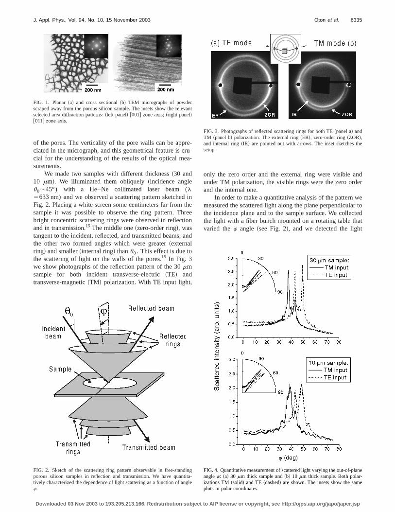
It is well known that the pores in heavily doped PS alarger than in lightly doped PS.16 We have investigated thegeometry of the microstructure with transmission electrmicroscopy~TEM! on a sample made with 50 mA/cm2 ofabout 30mm thickness. The micrographs shown in Fig.correspond to small pieces extracted by scraping the samwith a metallic blade. Figure 1~a! shows a top view of thesample. We can appreciate clearly that the pores are air hof ;50 nm diameter surrounded by thin (;10 nm) walls ofsilicon. In Fig. 1~b! one can observe the cross-sectional vi
:
4 © 2003 American Institute of Physics
AIP license or copyright, see http://ojps.aip.org/japo/japcr.jsp
reru
ea
dthre
tio
a
nder
wear toctedat
t
v
dintitng
he
lane
e
6335J. Appl. Phys., Vol. 94, No. 10, 15 November 2003 Oton et al.
of the pores. The verticality of the pore walls can be appciated in the micrograph, and this geometrical feature is ccial for the understanding of the results of the optical msurements.
We made two samples with different thickness~30 and10 mm!. We illuminated them obliquely~incidence angleu0;45°) with a He–Ne collimated laser beam (l5633 nm) and we observed a scattering pattern sketcheFig. 2. Placing a white screen some centimeters far fromsample it was possible to observe the ring pattern. Thbright concentric scattering rings were observed in reflecand in transmission.15 The middle one~zero-order ring!, wastangent to the incident, reflected, and transmitted beams,the other two formed angles which were greater~externalring! and smaller~internal ring! thanu0 . This effect is due tothe scattering of light on the walls of the pores.15 In Fig. 3we show photographs of the reflection pattern of the 30mmsample for both incident transverse-electric~TE! andtransverse-magnetic~TM! polarization. With TE input light,
FIG. 1. Planar~a! and cross sectional~b! TEM micrographs of powderscraped away from the porous silicon sample. The insets show the releselected area diffraction patterns:~left panel! @001# zone axis;~right panel!@011# zone axis.
FIG. 2. Sketch of the scattering ring pattern observable in free-stanporous silicon samples in reflection and transmission. We have quantively characterized the dependence of light scattering as a function of aw.
Downloaded 03 Nov 2003 to 193.205.213.166. Redistribution subject to
---
ineen
nd
only the zero order and the external ring were visible aunder TM polarization, the visible rings were the zero ordand the internal one.
In order to make a quantitative analysis of the patternmeasured the scattered light along the plane perpendiculthe incidence plane and to the sample surface. We collethe light with a fiber bunch mounted on a rotating table thvaried thew angle ~see Fig. 2!, and we detected the ligh
ant
ga-le
FIG. 3. Photographs of reflected scattering rings for both TE~panel a! andTM ~panel b! polarization. The external ring~ER!, zero-order ring~ZOR!,and internal ring~IR! are pointed out with arrows. The inset sketches tsetup.
FIG. 4. Quantitative measurement of scattered light varying the out-of-panglew: ~a! 30 mm thick sample and~b! 10 mm thick sample. Both polar-izations TM ~solid! and TE~dashed! are shown. The insets show the samplots in polar coordinates.
AIP license or copyright, see http://ojps.aip.org/japo/japcr.jsp
b
urhiP. WTt ore
inanicn
ne
ex.edte.of
alef an
onelar-
ro-
-
tureles
. 1,n betionois
ens,
les:
how
6336 J. Appl. Phys., Vol. 94, No. 10, 15 November 2003 Oton et al.
intensity with a silicon photodiode. Figure 4 shows the otained data.
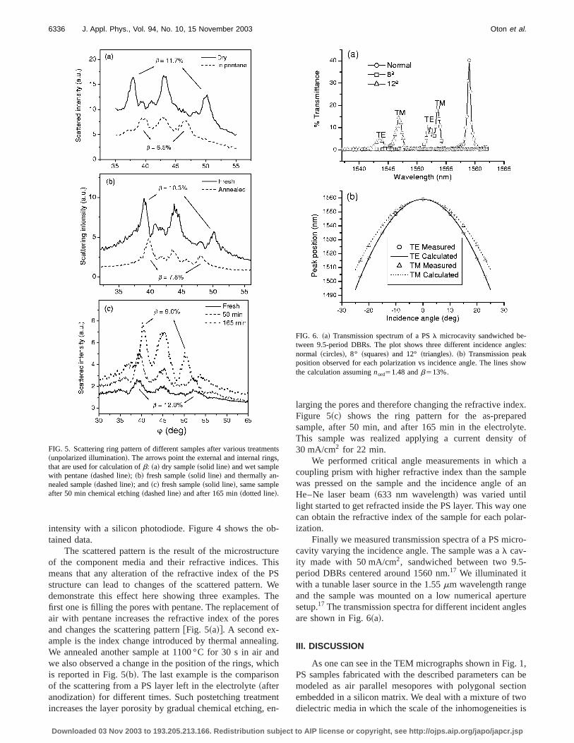
The scattered pattern is the result of the microstructof the component media and their refractive indices. Tmeans that any alteration of the refractive index of thestructure can lead to changes of the scattered patterndemonstrate this effect here showing three examples.first one is filling the pores with pentane. The replacemenair with pentane increases the refractive index of the poand changes the scattering pattern@Fig. 5~a!#. A second ex-ample is the index change introduced by thermal annealWe annealed another sample at 1100 °C for 30 s in airwe also observed a change in the position of the rings, whis reported in Fig. 5~b!. The last example is the comparisoof the scattering from a PS layer left in the electrolyte~afteranodization! for different times. Such postetching treatmeincreases the layer porosity by gradual chemical etching,
FIG. 5. Scattering ring pattern of different samples after various treatm~unpolarized illumination!. The arrows point the external and internal ringthat are used for calculation ofb: ~a! dry sample~solid line! and wet samplewith pentane~dashed line!; ~b! fresh sample~solid line! and thermally an-nealed sample~dashed line!; and~c! fresh sample~solid line!, same sampleafter 50 min chemical etching~dashed line! and after 165 min~dotted line!.
Downloaded 03 Nov 2003 to 193.205.213.166. Redistribution subject to
-
esS
ehefs
g.dh
tn-
larging the pores and therefore changing the refractive indFigure 5~c! shows the ring pattern for the as-preparsample, after 50 min, and after 165 min in the electrolyThis sample was realized applying a current density30 mA/cm2 for 22 min.
We performed critical angle measurements in whichcoupling prism with higher refractive index than the sampwas pressed on the sample and the incidence angle oHe–Ne laser beam~633 nm wavelength! was varied untillight started to get refracted inside the PS layer. This waycan obtain the refractive index of the sample for each poization.
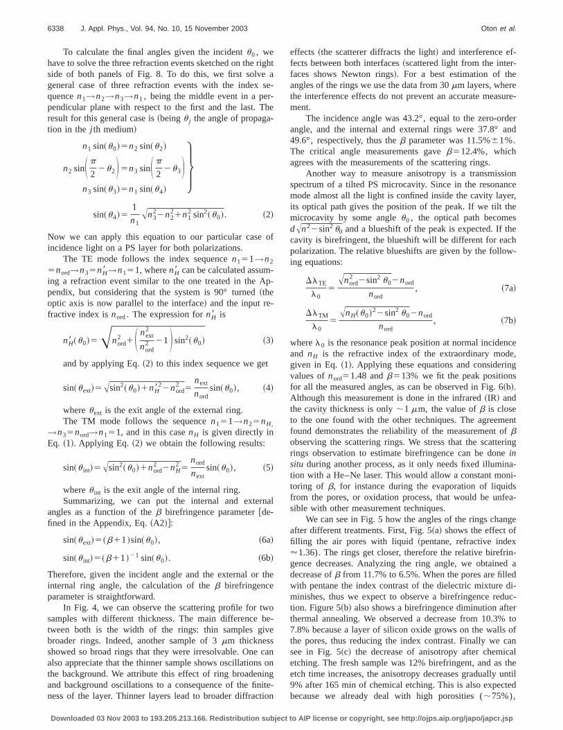
Finally we measured transmission spectra of a PS miccavity varying the incidence angle. The sample was al cav-ity made with 50 mA/cm2, sandwiched between two 9.5period DBRs centered around 1560 nm.17 We illuminated itwith a tunable laser source in the 1.55mm wavelength rangeand the sample was mounted on a low numerical apersetup.17 The transmission spectra for different incident angare shown in Fig. 6~a!.
III. DISCUSSION
As one can see in the TEM micrographs shown in FigPS samples fabricated with the described parameters camodeled as air parallel mesopores with polygonal secembedded in a silicon matrix. We deal with a mixture of twdielectric media in which the scale of the inhomogeneities
ts
FIG. 6. ~a! Transmission spectrum of a PSl microcavity sandwiched be-tween 9.5-period DBRs. The plot shows three different incidence angnormal ~circles!, 8° ~squares! and 12° ~triangles!. ~b! Transmission peakposition observed for each polarization vs incidence angle. The lines sthe calculation assumingnord51.48 andb513%.
AIP license or copyright, see http://ojps.aip.org/japo/japcr.jsp

re
ogh
idtria
eg
helti
instiooealca
inzatitryr
er
tivde
anor-
hecanionis.ion
he
umis
them
es
we
tog a
a-
ent
path
ticalthe
l therial.
6337J. Appl. Phys., Vol. 94, No. 10, 15 November 2003 Oton et al.
much smaller than the wavelength of visible light, therefothe medium optically behaves as homogeneous with anfective refractive index, which for~100!-orientedp1-type PSis optically anisotropic. However, despite the small sizethe microstructure, one could expect a small amount of lito scatter on the walls of the pores.
Let us approach the problem of light propagation insa PS layer by analyzing the scattering by an infinite dieleccylinder. In general one can define the intensity of light sctered with respect to both the azimuth anglej and the lati-tude anglew ~sketched in Fig. 7!. The azimuthal dependencof the scattered light can be calculated given the wavelenand polarization of light as well as the diameter of tcylinder.18 However, if the cylinder has perfectly parallewalls and infinite height, there is no light scattered with latudinal angles different fromw0 , even for columns with non-circular section. In this case, the so-called zero-order rappears~see Fig. 7!. If we suppose many parallel columndensely packed with a broad distribution of sizes and secshapes, we still expect to observe a ring, but with a smodependence onj. Modeling a PS layer as air pores embeddin silicon, one expects to observe a transmitted ring anda reflected one since the bottom surface of the layerreflect the whole pattern.
If the medium is optically anisotropic, as it happensour case, the different polarization modes must be analyseparately. If we assume a propagating ordinary wave thscattered by a cylinder, we expect to have some light wstill ordinary polarization, but also some with extraordinapolarization. Since the refractive index of the extraordinamode is different from the ordinary mode, the light undgoes a refraction event and the latitude anglew changes. Asthe extraordinary light propagates with a greater refracindex, the new angle with respect to the axis of the cylin
FIG. 7. Scattering of light by an infinitely long dielectric cylinder. Formtion of the zero-order ring. Definition of the scattering anglesw andj.
Downloaded 03 Nov 2003 to 193.205.213.166. Redistribution subject to
ef-
ft
ect-
th
-
g
nthdson
edish
y-
er
is larger in this case. The opposite effect can occur forincoming extraordinary mode that scatters and becomesdinary; as the refractive index change is from high to low, tnew angle will be smaller. To calculate these angles weapply Snell’s law the same way as studying a refractevent with an interface which is parallel to the cylinder axFigure 8 shows the scattering events for both polarizatmodes.
To calculate analytically the angles, we start solving tproblem of light initially propagating in an isotropic mediumthat encounters obliquely an anisotropic uniaxial mediwith a perpendicular optic axis. The Appendix solves thproblem in detail and arrives at an equation that givesrefractive index observed by a TM plane wave coming froan isotropic medium of indexniso with incident angleu0 ona uniaxial medium with ordinary and extraordinary indicnord and next. This refractive index lays betweennord andnext, and since it is higher than the ordinary mode index,call it nH
nH~u0!5nordA11niso2 S 1
nord2 2
1
next2 D sin2~u0!. ~1!
As shown in the Appendix, one can apply Snell’s lawthe wave front angle of the extraordinary mode assuminrefractive indexnH .
FIG. 8. Formation mechanism of the internal and external rings for incidTE ~panel a! and TM polarization~panel b!. The diagram on the left showsthe scattering event, and the schematic drawing on the right shows theof the light that comes from outside with a fixed angleu0 and gets refractedthree times. For making the ray-tracing clearer, we have drawn a verinterface and a hypothetical medium with another refractive index onright of the scattering event, but this refers to the scattered light along alazimuthal directions, and this event occurs everywhere inside the mate
AIP license or copyright, see http://ojps.aip.org/japo/japcr.jsp
riga
sr-h
-
o
-p
na
th
obeve
csinitio
-
ure-
derand
ionnceer,e
se
hw-
cee,g
entfring
a-ni-sea-
nge
in-d ad
di-uc-
erto
ofcanaltheuntilted
6338 J. Appl. Phys., Vol. 94, No. 10, 15 November 2003 Oton et al.
To calculate the final angles given the incidentu0 , wehave to solve the three refraction events sketched on theside of both panels of Fig. 8. To do this, we first solvegeneral case of three refraction events with the indexquencen1→n2→n3→n1 , being the middle event in a pependicular plane with respect to the first and the last. Tresult for this general case is~beingu j the angle of propagation in the j th medium!
n1 sin~u0!5n2 sin~u2!
n2 sinS p
22u2D5n3 sinS p
22u3D
n3 sin~u3!5n1 sin~u4!
Jsin~u4!5
1
n1An3
22n221n1
2 sin2~u0!. ~2!
Now we can apply this equation to our particular caseincidence light on a PS layer for both polarizations.
The TE mode follows the index sequencen151→n2
5nord→n35nH8 →n151, wherenH8 can be calculated assuming a refraction event similar to the one treated in the Apendix, but considering that the system is 90° turned~theoptic axis is now parallel to the interface! and the input re-fractive index isnord. The expression fornH8 is
nH8 ~u0!5Anord2 1S next
2
nord2 21D sin2~u0! ~3!
and by applying Eq.~2! to this index sequence we get
sin~uext!5Asin2~u0!1nH822nord
2 5next
nordsin~u0!, ~4!
whereuext is the exit angle of the external ring.The TM mode follows the sequencen151→n25nH,
→n35nord→n151, and in this casenH is given directly inEq. ~1!. Applying Eq. ~2! we obtain the following results:
sin~u int!5Asin2~u0!1nord2 2nH
2 5nord
nextsin~u0!, ~5!
whereu int is the exit angle of the internal ring.Summarizing, we can put the internal and exter
angles as a function of theb birefringence parameter@de-fined in the Appendix, Eq.~A2!#:
sin~uext!5~b11!sin~u0!, ~6a!
sin~u int!5~b11!21 sin~u0!. ~6b!
Therefore, given the incident angle and the external orinternal ring angle, the calculation of theb birefringenceparameter is straightforward.
In Fig. 4, we can observe the scattering profile for twsamples with different thickness. The main differencetween both is the width of the rings: thin samples gibroader rings. Indeed, another sample of 3mm thicknessshowed so broad rings that they were irresolvable. Onealso appreciate that the thinner sample shows oscillationthe background. We attribute this effect of ring broadenand background oscillations to a consequence of the finness of the layer. Thinner layers lead to broader diffract
Downloaded 03 Nov 2003 to 193.205.213.166. Redistribution subject to
ht
e-
e
f
-
l
e
-
anonge-n
effects~the scatterer diffracts the light! and interference ef-fects between both interfaces~scattered light from the interfaces shows Newton rings!. For a best estimation of theangles of the rings we use the data from 30mm layers, wherethe interference effects do not prevent an accurate measment.
The incidence angle was 43.2°, equal to the zero-orangle, and the internal and external rings were 37.8°49.6°, respectively, thus theb parameter was 11.5%61%.The critical angle measurements gaveb512.4%, whichagrees with the measurements of the scattering rings.
Another way to measure anisotropy is a transmissspectrum of a tilted PS microcavity. Since in the resonamode almost all the light is confined inside the cavity layits optical path gives the position of the peak. If we tilt thmicrocavity by some angleu0 , the optical path becomedAn22sin2 u0 and a blueshift of the peak is expected. If thcavity is birefringent, the blueshift will be different for eacpolarization. The relative blueshifts are given by the folloing equations:
DlTE
l05
Anord2 2sin2 u02nord
nord, ~7a!
DlTM
l05
AnH~u0!22sin2 u02nord
nord, ~7b!
wherel0 is the resonance peak position at normal incidenand nH is the refractive index of the extraordinary modgiven in Eq.~1!. Applying these equations and considerinvalues ofnord51.48 andb513% we fit the peak positionsfor all the measured angles, as can be observed in Fig. 6~b!.Although this measurement is done in the infrared~IR! andthe cavity thickness is only;1 mm, the value ofb is closeto the one found with the other techniques. The agreemfound demonstrates the reliability of the measurement obobserving the scattering rings. We stress that the scatterings observation to estimate birefringence can be doneinsitu during another process, as it only needs fixed illumintion with a He–Ne laser. This would allow a constant motoring of b, for instance during the evaporation of liquidfrom the pores, or oxidation process, that would be unfsible with other measurement techniques.
We can see in Fig. 5 how the angles of the rings chaafter different treatments. First, Fig. 5~a! shows the effect offilling the air pores with liquid~pentane, refractive index'1.36). The rings get closer, therefore the relative birefrgence decreases. Analyzing the ring angle, we obtainedecrease ofb from 11.7% to 6.5%. When the pores are fillewith pentane the index contrast of the dielectric mixtureminishes, thus we expect to observe a birefringence redtion. Figure 5~b! also shows a birefringence diminution aftthermal annealing. We observed a decrease from 10.3%7.8% because a layer of silicon oxide grows on the wallsthe pores, thus reducing the index contrast. Finally wesee in Fig. 5~c! the decrease of anisotropy after chemicetching. The fresh sample was 12% birefringent, and asetch time increases, the anisotropy decreases gradually9% after 165 min of chemical etching. This is also expecbecause we already deal with high porosities (;75%),
AIP license or copyright, see http://ojps.aip.org/japo/japcr.jsp
ble-p
mettneetnifW
tice
ISort.
so
-elth
ire
c-
a
lvpulp
d
aveisivepa-a-
le
ryn
e
h,
thewnth
6339J. Appl. Phys., Vol. 94, No. 10, 15 November 2003 Oton et al.
hence even higher porosities unbalance more the mixtween silicon and air, thus the optical properties becomeanisotropic.19 It is also worth noticing the increase in intensity of the rings, which is probably due to lower light absortion of higher porosity porous silicon.20
IV. CONCLUSIONS
In this work we studied the light scattering mechanisin heavily doped~100!-oriented porous silicon layers. Wsuccessfully measured birefringence by analyzing the scaing rings, and we compare the results with values obtaiwith critical angle measurements and with angle-dependtransmission spectra, finding good agreement. We studybirefringence changes when pores are filled with pentaafter thermal annealing, and after chemical etching for dferent times, and in all cases birefringence decreases.propose this technique as a useful tool to measure opanisotropy far from the sample, since it only requires a fixoblique illumination with a laser beam.
ACKNOWLEDGMENTS
The authors acknowledge INFM Section E Project PARANDS 2001 and Science and Technology MinistrySpain Project No. MAT 2002-00044 for financial suppoThey thank L. Zampedri for them-line measurements and DS. Wiersma for fruitful discussions.
APPENDIX
Uniaxial media are characterized by a dielectric tenthat can take the simple form~in a system of principal axes!
S Dx
Dy
Dz
D 5S «ord 0 0
0 «ord 0
0 0 «ext
D S Ex
Ey
Ez
D , ~A1!
whereDx,y,z and Ex,y,z are the components of the displacement vector and the electric field vector, respectivThese media are characterized only by the direction ofoptic axis~in this case, thez direction! and the ordinary andextraordinary permitivities«ord and«ext. The square root ofthese values are the ordinary and extraordinary refractivedicesnord and next. Other parameters usually employed athebirefringenceDn, and theb parameter which are, respetively
Dn5next2nord, ~A2a!
b5Dn
nord. ~A2b!
When light encounters obliquely an interface betweenisotropic ~index niso) and a uniaxial medium~indices nord
and next), double refraction occurs, thus one has to soseparately the TE and the TM modes. The TE mode progates isotropically because the electric field is perpendicto the optic axis for every angle. For this case we can apSnell’s law assumingnord to be the refractive index of theanisotropic medium as follows:
nisosin~u0!5nordsin~uord!. ~A3!
Downloaded 03 Nov 2003 to 193.205.213.166. Redistribution subject to
e-ss
-
er-dnthee,-e
ald
-f.
r
y.e
n-
n
ea-arly
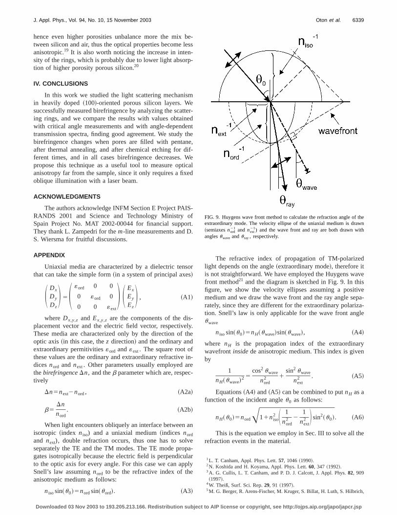
The refractive index of propagation of TM-polarizelight depends on the angle~extraordinary mode!, therefore itis not straightforward. We have employed the Huygens wfront method21 and the diagram is sketched in Fig. 9. In thfigure, we show the velocity ellipses assuming a positmedium and we draw the wave front and the ray angle serately, since they are different for the extraordinary polariztion. Snell’s law is only applicable for the wave front anguwave
nisosin~u0!5nH~uwave!sin~uwave!, ~A4!
where nH is the propagation index of the extraordinawavefrontinsidede anisotropic medium. This index is giveby
1
nH~uwave!2 5
cos2 uwave
nord2 1
sin2 uwave
next2 . ~A5!
Equations~A4! and~A5! can be combined to putnH as afunction of the incident angleu0 as follows:
nH~u0!5nordA11niso2 S 1
nord2 2
1
next2 D sin2~u0!. ~A6!
This is the equation we employ in Sec. III to solve all threfraction events in the material.
1L. T. Canham, Appl. Phys. Lett.57, 1046~1990!.2N. Koshida and H. Koyama, Appl. Phys. Lett.60, 347 ~1992!.3A. G. Cullis, L. T. Canham, and P. D. J. Calcott, J. Appl. Phys.82, 909~1997!.
4W. Theiß, Surf. Sci. Rep.29, 91 ~1997!.5M. G. Berger, R. Arens-Fischer, M. Kruger, S. Billat, H. Luth, S. Hilbric
FIG. 9. Huygens wave front method to calculate the refraction angle ofextraordinary mode. The velocity ellipse of the uniaxial medium is dra~semiaxesnord
21 and next21) and the wave front and ray are both drawn wi
anglesuwave andu ray , respectively.
AIP license or copyright, see http://ojps.aip.org/japo/japcr.jsp

pl
H.
al
pl.
ett.
,
6340 J. Appl. Phys., Vol. 94, No. 10, 15 November 2003 Oton et al.
W. Theiß, and P. Grosse, Thin Solid Films297, 137 ~1997!.6V. Agarwal and J. A. del Rio, Appl. Phys. Lett.82, 1512~2003!.7L. Pavesi, Riv. Nuovo Cimento20, 1 ~1997!.8M. Ghulinyan, C. J. Oton, Z. Gaburro, P. Bettotti, and L. Pavesi, ApPhys. Lett.82, 1550~2003!.
9P. Ferrand, R. Romestain, and J. C. Vial, Phys. Rev. B63, 115106~2001!.10M. Kruger et al., Jpn. J. Appl. Phys., Part 236, L24 ~1997!.11F. Ferrieu, A. Halimaoui, and D. Bensahel, Solid State Commun.84, 293
~1992!.12P. Basmaji, G. Surdutovich, R. Vitlina, J. Kolenda, V. S. Bagnato,
Mohajeri-Moghaddam, and N. Peyghambariam, Solid State Commun91,649 ~1994!.
13H. Kryzanowska, M. Kulik, and J. Zuk, J. Lumin.80, 183 ~1999!.14D. Kovalev, G. Polisski, J. Diener, H. Heckler, N. Ku¨nzner, V. Yu. Ti-
Downloaded 03 Nov 2003 to 193.205.213.166. Redistribution subject to
.
.
moshenko, and F. Koch, Appl. Phys. Lett.78, 916 ~2001!.15C. J. Oton, Z. Gaburro, M. Ghulinyan, L. Pancheri, P. Bettotti, L. D
Negro, and L. Pavesi, Appl. Phys. Lett.81, 4919~2002!.16G. Bomchilet al., Appl. Surf. Sci.65Õ66, 394 ~1993!.17M. Ghulinyan, C. J. Oton, G. Bonetti, Z. Gaburro, and L. Pavesi, J. Ap
Phys.93, 9724~2003!.18C. F. Bohren and D. R. Huffman,Absorption and Scattering of Light by
Small Particles~Wiley, New York, 1983!, p. 194.19F. Genereux, S. W. Leonard, H. M. Van Driel, A. Birner, and U. Go¨sele,
Phys. Rev. B63, 161101~2001!.20I. Sagnes, A. Halimaoui, G. Vincent, and P. A. Badoz, Appl. Phys. L
62, 1155~1993!.21M. Born and E. Wolf,Principles of Optics~Cambridge University Press
Cambridge, 1980!.
AIP license or copyright, see http://ojps.aip.org/japo/japcr.jsp