Silicon Detectors - CERN Indico
71
Silicon Detectors Manfred Krammer Frank Hartmann Institute of High Energy Physics Karlsruhe Institute of Technology Vienna, Austria Karlsruhe, Germany
-
Upload
khangminh22 -
Category
Documents
-
view
1 -
download
0
Transcript of Silicon Detectors - CERN Indico
Silicon Detectors !
Manfred Krammer ! ! !Frank Hartmann!
Institute of High Energy Physics !Karlsruhe Institute of Technology! Vienna, Austria ! ! !Karlsruhe, Germany!
Content!
Silicon Detectors! 1!
1 Material Properties!2 Detector Structures!
3 Performance!
4 Detector Systems!
M. Krammer, F. Hartmann EDIT 2011!
Silicon Detectors! 2!
1 Material Properties!
M. Krammer, F. Hartmann EDIT 2011!
Silicon Detectors! 3!
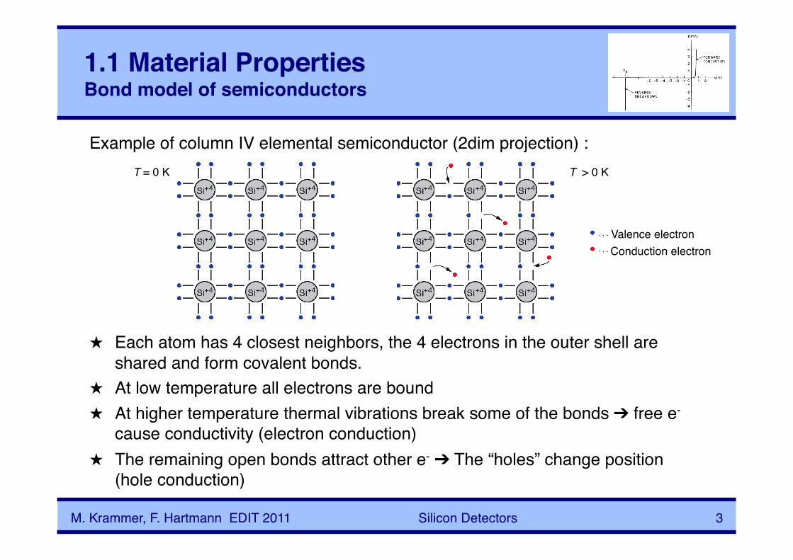
1.1 Material Properties Bond model of semiconductors!
Example of column IV elemental semiconductor (2dim projection) :!
★ Each atom has 4 closest neighbors, the 4 electrons in the outer shell are shared and form covalent bonds.!
★ At low temperature all electrons are bound!★ At higher temperature thermal vibrations break some of the bonds ➔ free e-
cause conductivity (electron conduction)!★ The remaining open bonds attract other e- ➔ The “holes” change position
(hole conduction)!
T = 0 K! T > 0 K!
Conduction electron!Valence electron!
M. Krammer, F. Hartmann EDIT 2011!

Silicon Detectors! 4!
1.1 Material Properties Energy bands: isolator–semiconductor–metal!
In an isolated atom the electrons have only discrete energy levels. In solid state material the atomic levels merge to energy bands. In metals the conduction and the valence band overlap, whereas in isolators and semiconductors these levels are separated by an energy gap (band gap). In isolators this gap is large.!
M. Krammer, F. Hartmann EDIT 2011!
Silicon Detectors! 5!
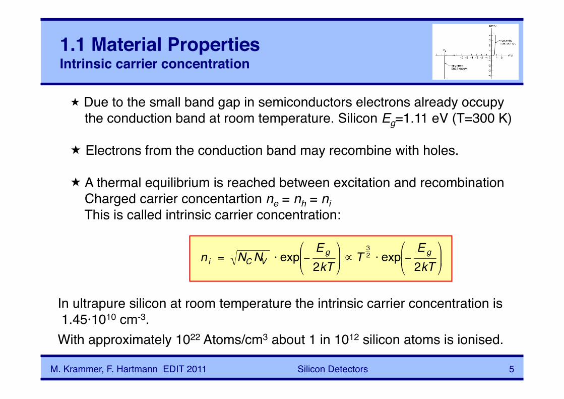
1.1 Material Properties Intrinsic carrier concentration!
Due to the small band gap in semiconductors electrons already occupy! the conduction band at room temperature. Silicon Eg=1.11 eV (T=300 K)!
Electrons from the conduction band may recombine with holes.!
A thermal equilibrium is reached between excitation and recombination! Charged carrier concentartion ne = nh = ni ! This is called intrinsic carrier concentration:!
In ultrapure silicon at room temperature the intrinsic carrier concentration is 1.45·1010 cm-3. !With approximately 1022 Atoms/cm3 about 1 in 1012 silicon atoms is ionised.!
M. Krammer, F. Hartmann EDIT 2011!
Silicon Detectors! 6!
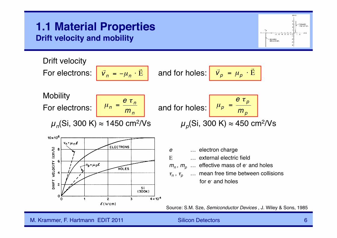
1.1 Material Properties Drift velocity and mobility!
Drift velocity!For electrons: ! ! !and for holes:!
Mobility!For electrons: ! ! !and for holes:!
e !… !electron charge !!Ε !… external electric field!mn , mp !… !effective mass of e- and holes!τn , τp !… !mean free time between collisions!
! for e- and holes!
Source: S.M. Sze, Semiconductor Devices , J. Wiley & Sons, 1985!
µn(Si, 300 K) ≈ 1450 cm2/Vs! µp(Si, 300 K) ≈ 450 cm2/Vs!
M. Krammer, F. Hartmann EDIT 2011!
Silicon Detectors! 7!
1.2 Constructing a Detector The ideal semiconductor detector!
Charged particles penetrating or traversing the detector create electron-hole pairs. The electron-hole pairs are separated by an electric field and drift to the electrodes. This is the signal we are looking for.! One of the most important parameter of a detector is the signal to noise ratio (SNR). A good detector should have a large SNR. However this leads to two contradictory requirements:!
✘ Large signal➔ particles should produce many electron-holes ➔ low ionization energy ➔ small band gap!
✘ Low noise➔ very few intrinsic charge carriers ➔ large band gap!
M. Krammer, F. Hartmann EDIT 2011!
Silicon Detectors! 8!
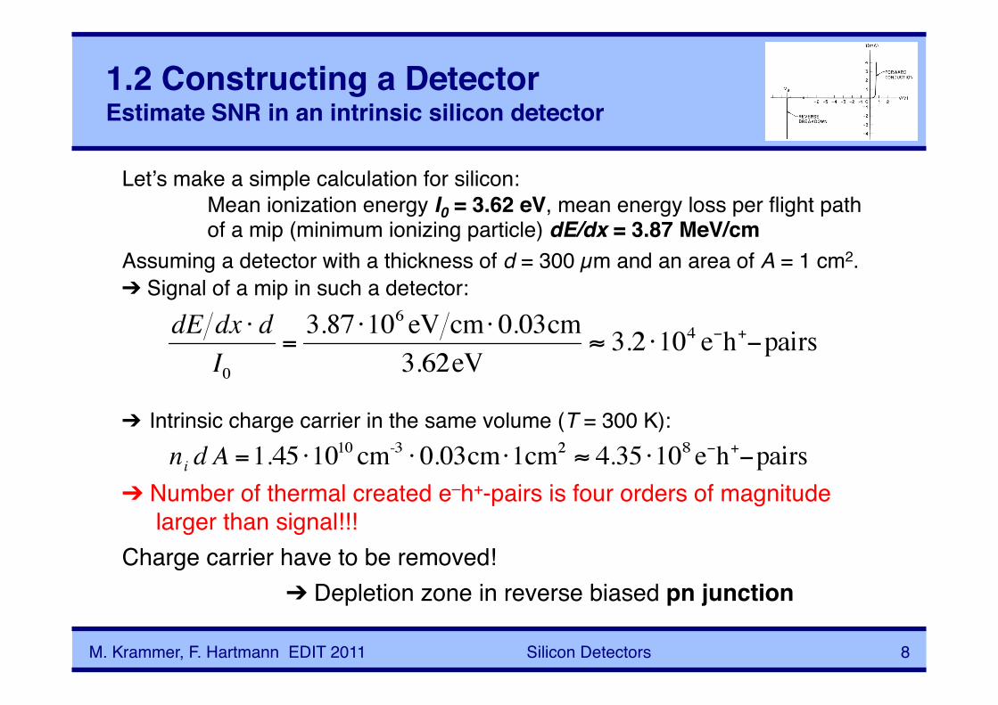
1.2 Constructing a Detector Estimate SNR in an intrinsic silicon detector!
Letʼs make a simple calculation for silicon: ! ! ! !!Mean ionization energy I0 = 3.62 eV, mean energy loss per flight path
!of a mip (minimum ionizing particle) dE/dx = 3.87 MeV/cm!Assuming a detector with a thickness of d = 300 µm and an area of A = 1 cm2.!➔ Signal of a mip in such a detector:!
Charge carrier have to be removed! !! !➔ Depletion zone in reverse biased pn junction!
➔ !Intrinsic charge carrier in the same volume (T = 300 K):!
➔ Number of thermal created e–h+-pairs is four orders of magnitude larger than signal!!!!
M. Krammer, F. Hartmann EDIT 2011!
Silicon Detectors! 9!
1.2 Doping pn junction needs doped materials!
★ Doping is the replacement of a small number of atoms in the lattice by atoms of neighboring columns from the atomic table (with one valence electron more or less compared to the basic material). Typical doping concentrations for Si detectors are ≈1012 atoms/cm3
(1014 und 1018 atoms/cm3 for CMOS elements). !
★ These doping atoms create energy levels within the band gap and therefore alter the conductivity.!
★ An undoped semiconductor is called an intrinsic semiconductor!
★ A doped semiconductor is called an extrinsic semiconductor.!
★ In an intrinsic semiconductor for each conduction electron there exists the corresponding hole. In extrinsic semiconductors there is a surplus of electrons or holes.!
A pn junction consists of n and p doped substrates:!
M. Krammer, F. Hartmann EDIT 2011!
Silicon Detectors! 10!
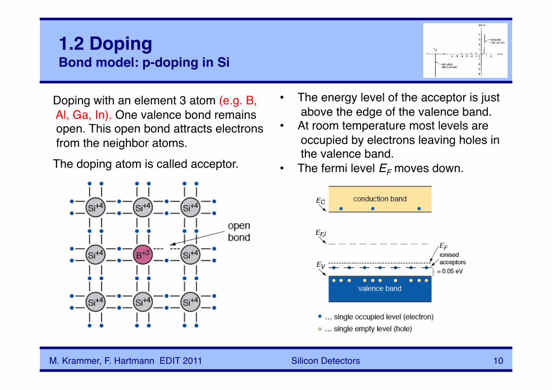
1.2 Doping Bond model: p-doping in Si!
• The energy level of the acceptor is just above the edge of the valence band. !
• At room temperature most levels are occupied by electrons leaving holes in the valence band.!
• The fermi level EF moves down. !
M. Krammer, F. Hartmann EDIT 2011!
Doping with an element 3 atom (e.g. B, Al, Ga, In). One valence bond remains open. This open bond attracts electrons from the neighbor atoms.!The doping atom is called acceptor. !
Silicon Detectors! 11!
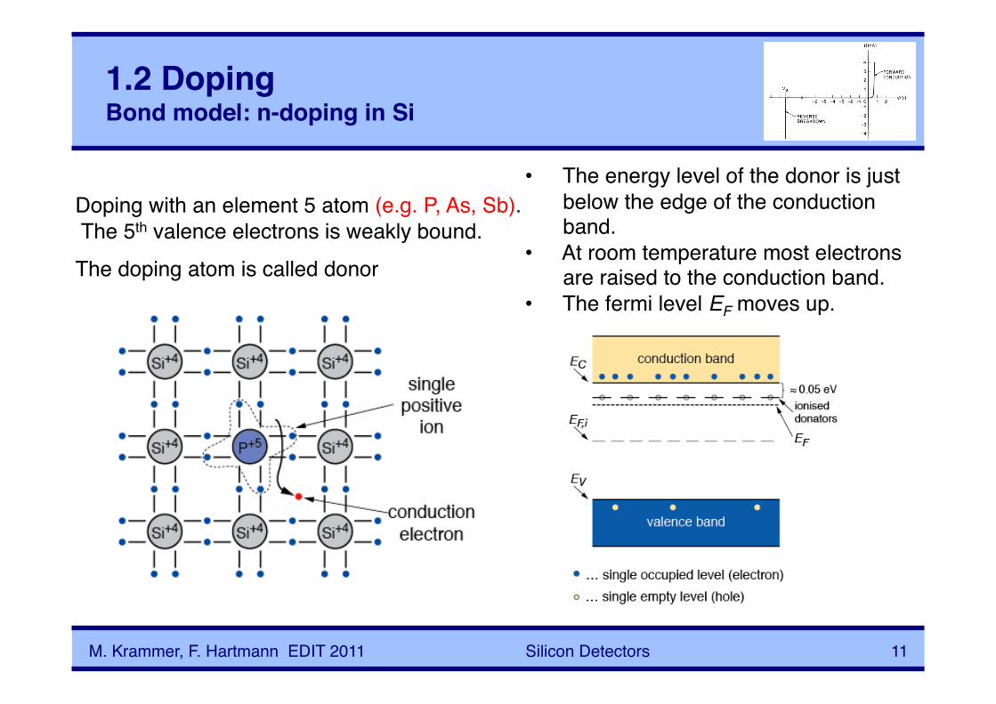
1.2 Doping Bond model: n-doping in Si!
• The energy level of the donor is just below the edge of the conduction band. !
• At room temperature most electrons are raised to the conduction band.!
• The fermi level EF moves up. !
M. Krammer, F. Hartmann EDIT 2011!
Doping with an element 5 atom (e.g. P, As, Sb). The 5th valence electrons is weakly bound.!The doping atom is called donor!
Silicon Detectors! 12!
1.3 The p-n JunctionCreating a p-n junction!
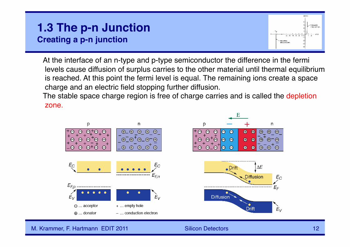
At the interface of an n-type and p-type semiconductor the difference in the fermi levels cause diffusion of surplus carries to the other material until thermal equilibrium is reached. At this point the fermi level is equal. The remaining ions create a space charge and an electric field stopping further diffusion.!The stable space charge region is free of charge carries and is called the depletion zone.!
M. Krammer, F. Hartmann EDIT 2011!

Silicon Detectors! 13!
1.3 The p-n JunctionElectrical characteristics!
M. Krammer, F. Hartmann EDIT 2011!
Silicon Detectors! 14!
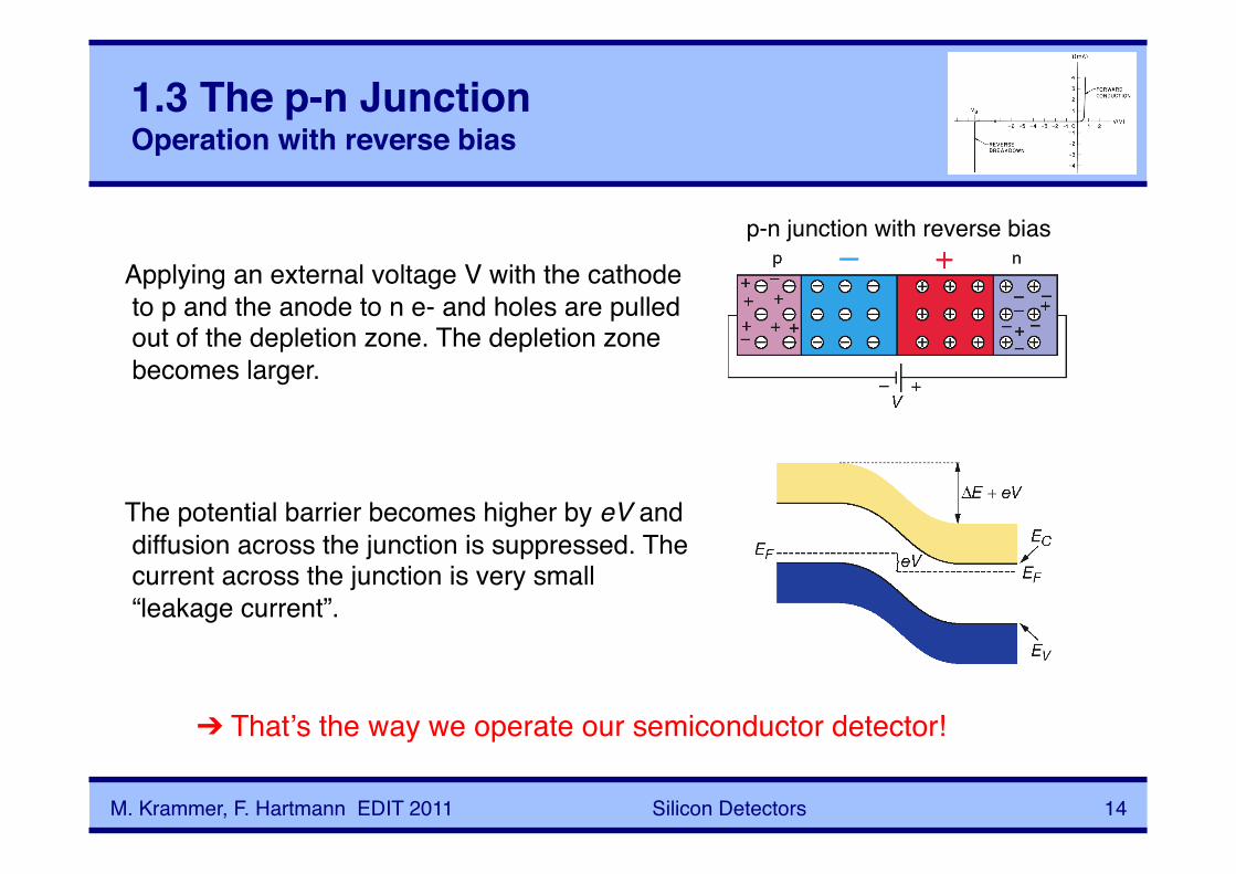
1.3 The p-n JunctionOperation with reverse bias!
p-n junction with reverse bias!
Applying an external voltage V with the cathode to p and the anode to n e- and holes are pulled out of the depletion zone. The depletion zone becomes larger.!
The potential barrier becomes higher by eV and diffusion across the junction is suppressed. The current across the junction is very small “leakage current”.!
➔ Thatʼs the way we operate our semiconductor detector!!
M. Krammer, F. Hartmann EDIT 2011!
Silicon Detectors! 15!
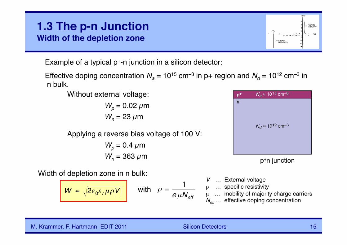
Example of a typical p+-n junction in a silicon detector:!
Effective doping concentration Na = 1015 cm–3 in p+ region and Nd = 1012 cm–3 in n bulk.!
1.3 The p-n JunctionWidth of the depletion zone!
p+n junction!
Without external voltage:!Wp = 0.02 µm !Wn = 23 µm!
Applying a reverse bias voltage of 100 V:!Wp = 0.4 µm !Wn = 363 µm!
with!V !… !External voltage ρ !… !specific resistivity!µ !… !mobility of majority charge carriers!Neff!… !effective doping concentration!
Width of depletion zone in n bulk:!
M. Krammer, F. Hartmann EDIT 2011!
1.3 n-type and p-type Detectors!
M. Krammer, F. Hartmann EDIT 2011! Silicon Detectors! 16!
Note:!
The previous slide explains an n-type detector (detector bulk is n-type silicon)!
Using p-type silicon and exchanging p+ and n+ would give a perfectly working p-type detector. !
For tradition and production reasons most detectors used are n-type detectors. p-type detectors have some advantages in high radiation environment (see later).!
For simplicity I will continue discussing n-type detectors only...!

Silicon Detectors! 17!
1.3 The p-n JunctionCurrent-voltage characteristics!
Typical current-voltage of a p-n junction (diode): exponential current increase in forward bias, small saturation in reverse bias.!
S.M. Sze, Semiconductor Devices , J. Wiley & Sons, 1985!
M. Krammer, F. Hartmann EDIT 2011!
Operation mode!
Silicon Detectors! 18!
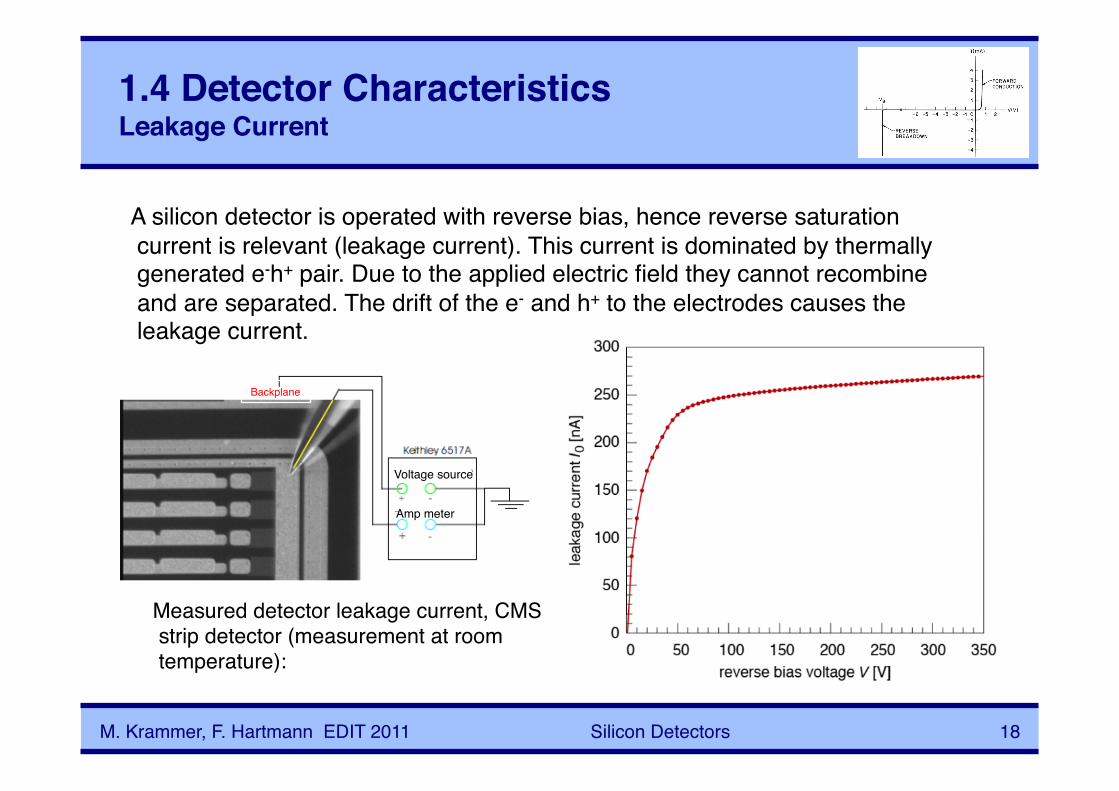
1.4 Detector Characteristics Leakage Current!
Measured detector leakage current, CMS strip detector (measurement at room temperature):!
A silicon detector is operated with reverse bias, hence reverse saturation current is relevant (leakage current). This current is dominated by thermally generated e-h+ pair. Due to the applied electric field they cannot recombine and are separated. The drift of the e- and h+ to the electrodes causes the leakage current. !
M. Krammer, F. Hartmann EDIT 2011!
Backplane!
Voltage source!
Amp meter!
Silicon Detectors! 19!
ρ !… !specific resistivity of the bulk!µ !… !mobility of majority charge carrier!V !… !bias voltage !!A !… !detector surface!D !… detector thickness!
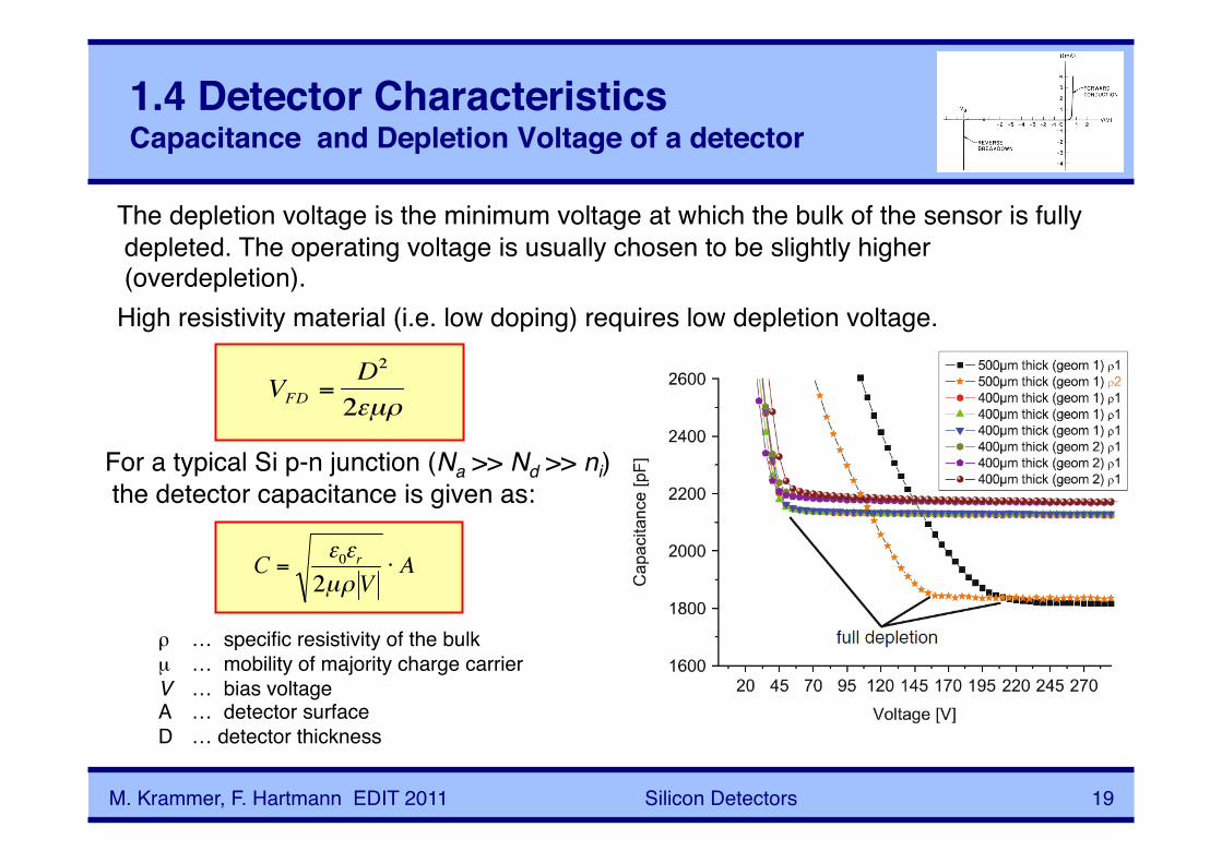
1.4 Detector Characteristics Capacitance and Depletion Voltage of a detector!
For a typical Si p-n junction (Na >> Nd >> ni) the detector capacitance is given as:!
Measured detector capacitance as a function of the bias voltage, CMS strip detector:!
The depletion voltage is the minimum voltage at which the bulk of the sensor is fully depleted. The operating voltage is usually chosen to be slightly higher (overdepletion).!High resistivity material (i.e. low doping) requires low depletion voltage.!
M. Krammer, F. Hartmann EDIT 2011!
Silicon Detectors! 20!
2 Detector Structures!
M. Krammer, F. Hartmann EDIT 2011!
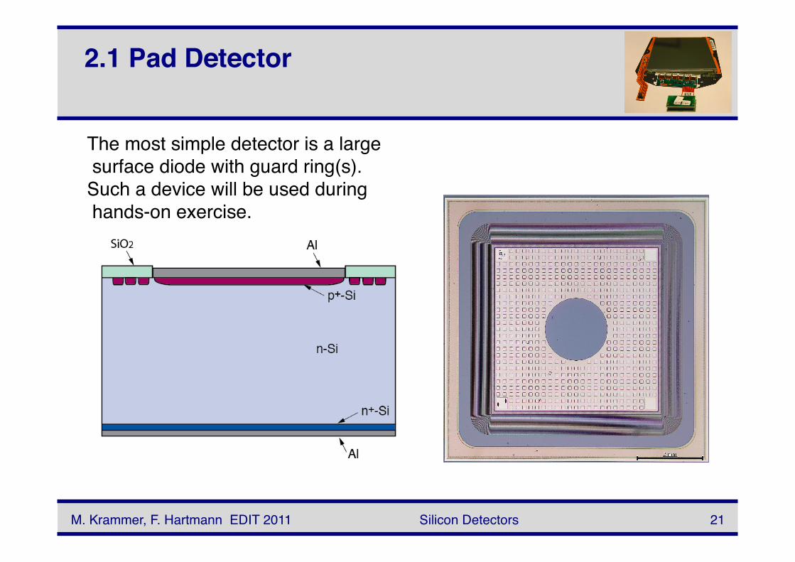
2.1 Pad Detector
Silicon Detectors! 21!
The most simple detector is a large surface diode with guard ring(s).!Such a device will be used during hands-on exercise.!
M. Krammer, F. Hartmann EDIT 2011!
2.2 Microstrip Detector DC coupled strip detector!
Silicon Detectors! 22!
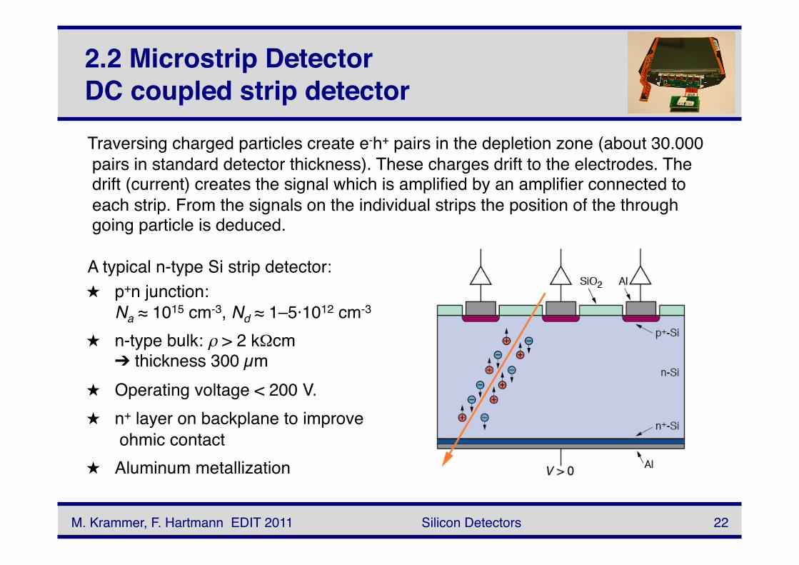
★ p+n junction: Na ≈ 1015 cm-3, Nd ≈ 1–5·1012 cm-3!
★ n-type bulk: ρ > 2 kΩcm➔ thickness 300 µm !
★ Operating voltage < 200 V.!★ n+ layer on backplane to improve
ohmic contact!★ Aluminum metallization !
Traversing charged particles create e-h+ pairs in the depletion zone (about 30.000 pairs in standard detector thickness). These charges drift to the electrodes. The drift (current) creates the signal which is amplified by an amplifier connected to each strip. From the signals on the individual strips the position of the through going particle is deduced. !
A typical n-type Si strip detector:!
M. Krammer, F. Hartmann EDIT 2011!
2.2 Microstrip Detector AC coupled strip detector!
Silicon Detectors! 23!
★ Integration of coupling capacitances in standard planar process.!
★ Deposition of SiO2 with a thickness of 100–200 nm between p+ and aluminum strip!
★ Depending on oxide thickness and strip width the capacitances are in the range of 8–32 pF/cm.!
★ Problems are shorts through the dielectric (pinholes). Usually avoided by a second layer of Si3N4.!
AC coupled strip detector:!
Several methods to connect the bias voltage: polysilicon resistor, punch through bias, FOXFET bias.!
AC coupling blocks leakage current from the amplifier.!
M. Krammer, F. Hartmann EDIT 2011!
2.2 Microstrip Detector Polysilicon bias resistor!
Silicon Detectors! 24!
★ Deposition of polycristalline silicon between p+ implants and a common bias line. !
★ Sheet resistance of up to Rs ≈ 250 kΩ/❏. Depending on width and length a resistor of up to R ≈ 20 MΩ is achieved (R = Rs·length/width).!
★ To achieve high resistor values winding poly structures are deposited.!
CMS Collaboration, HEPHY Vienna!Cut through an AC coupled strip detector with integrated poly resistors:!
M. Krammer, F. Hartmann EDIT 2011!
2.2 Electrical Field Configuration of a Strip Sensor!
Silicon Detectors! 25!M. Krammer, F. Hartmann EDIT 2011!
2.2. Electrical Field across a Strip!
Silicon Detectors! 26!M. Krammer, F. Hartmann EDIT 2011!
Elec
trica
l Fie
ld [
V/cm
]!
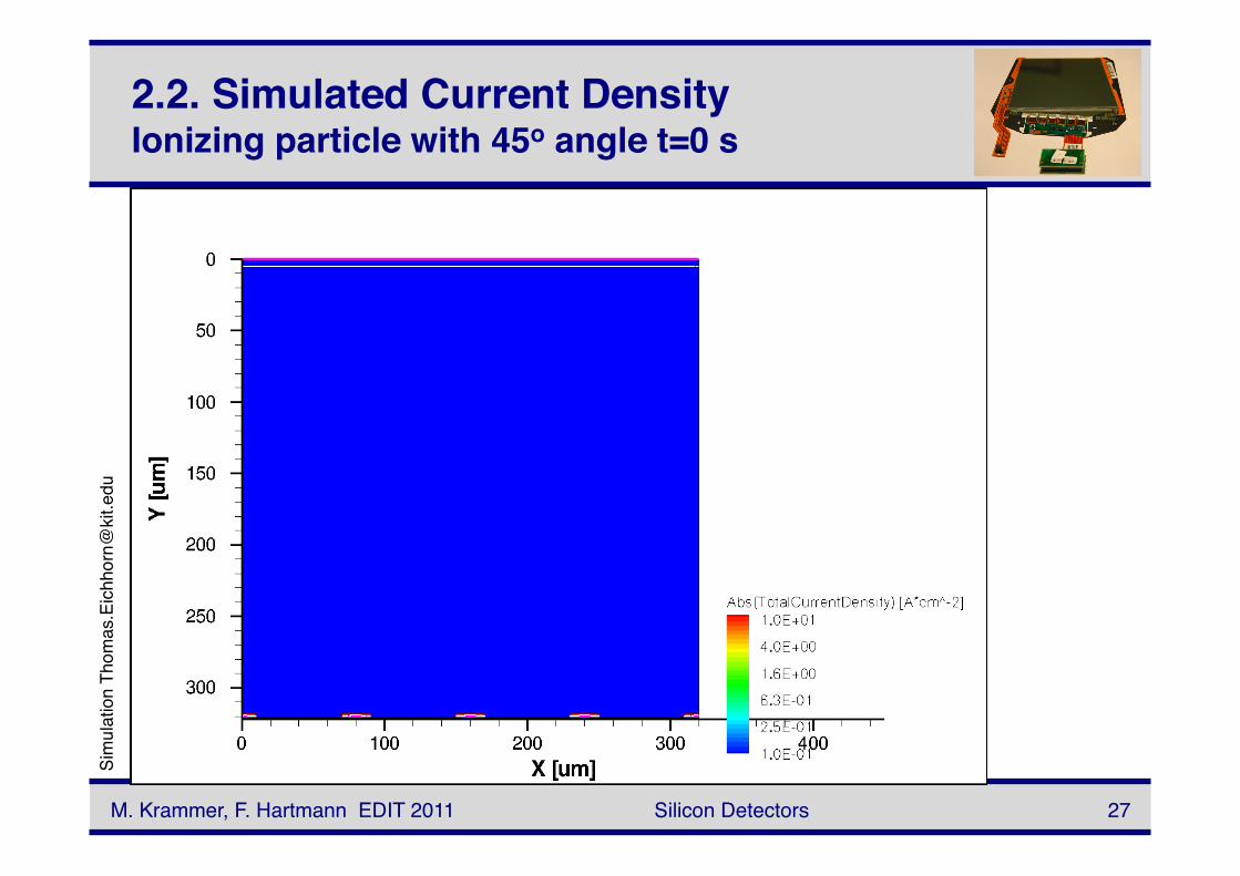
2.2. Simulated Current Density Ionizing particle with 45o angle t=0 s!
Silicon Detectors! 27!
Sim
ulat
ion
Thom
as.E
ichh
orn@
kit.e
du!
M. Krammer, F. Hartmann EDIT 2011!
Silicon Detectors! 28!
Sim
ulat
ion
Thom
as.E
ichh
orn@
kit.e
du!
M. Krammer, F. Hartmann EDIT 2011!
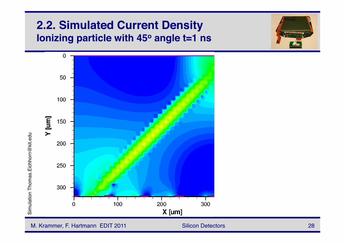
2.2. Simulated Current Density Ionizing particle with 45o angle t=1 ns!
Silicon Detectors! 29!
Sim
ulat
ion
Thom
as.E
ichh
orn@
kit.e
du!
M. Krammer, F. Hartmann EDIT 2011!
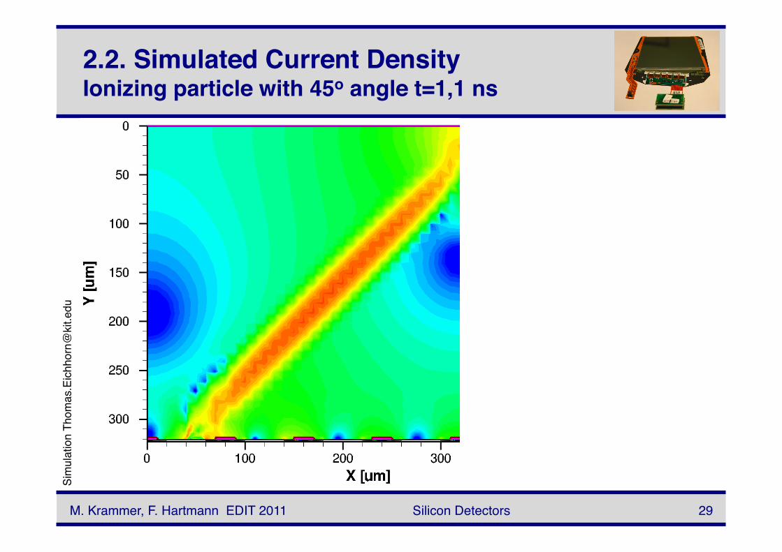
2.2. Simulated Current Density Ionizing particle with 45o angle t=1,1 ns!
Silicon Detectors! 30!
Sim
ulat
ion
Thom
as.E
ichh
orn@
kit.e
du!
M. Krammer, F. Hartmann EDIT 2011!
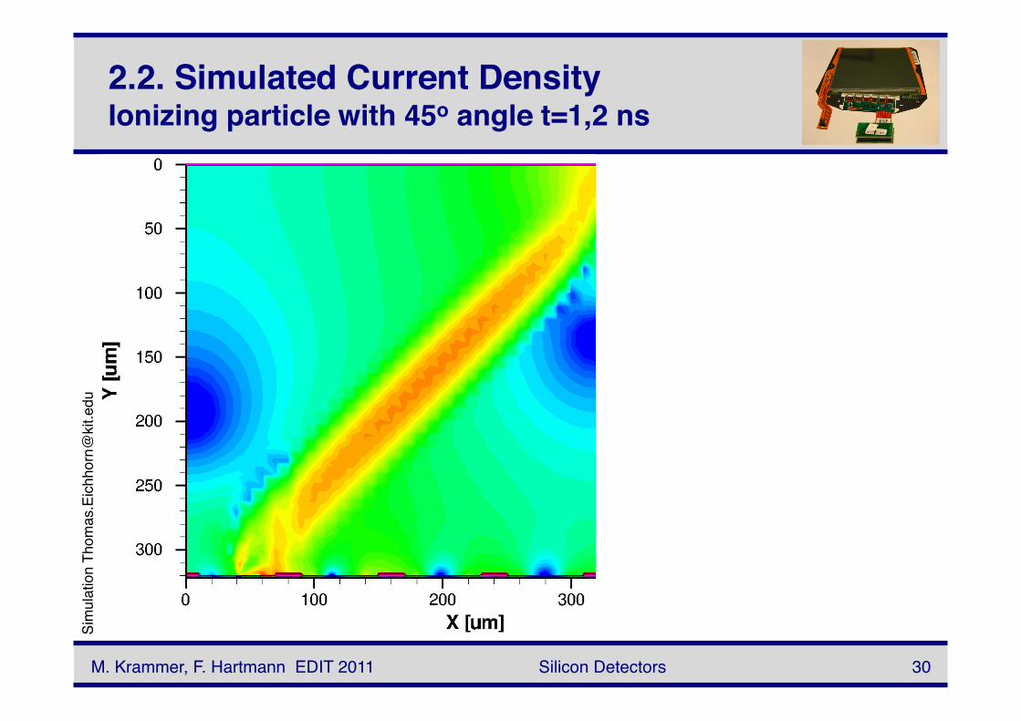
2.2. Simulated Current Density Ionizing particle with 45o angle t=1,2 ns!
Silicon Detectors! 31!
Sim
ulat
ion
Thom
as.E
ichh
orn@
kit.e
du!
M. Krammer, F. Hartmann EDIT 2011!
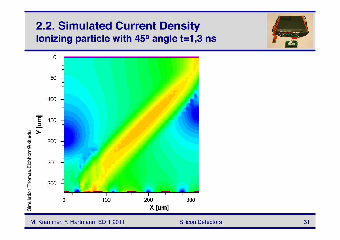
2.2. Simulated Current Density Ionizing particle with 45o angle t=1,3 ns!
Silicon Detectors! 32!
Sim
ulat
ion
Thom
as.E
ichh
orn@
kit.e
du!
M. Krammer, F. Hartmann EDIT 2011!
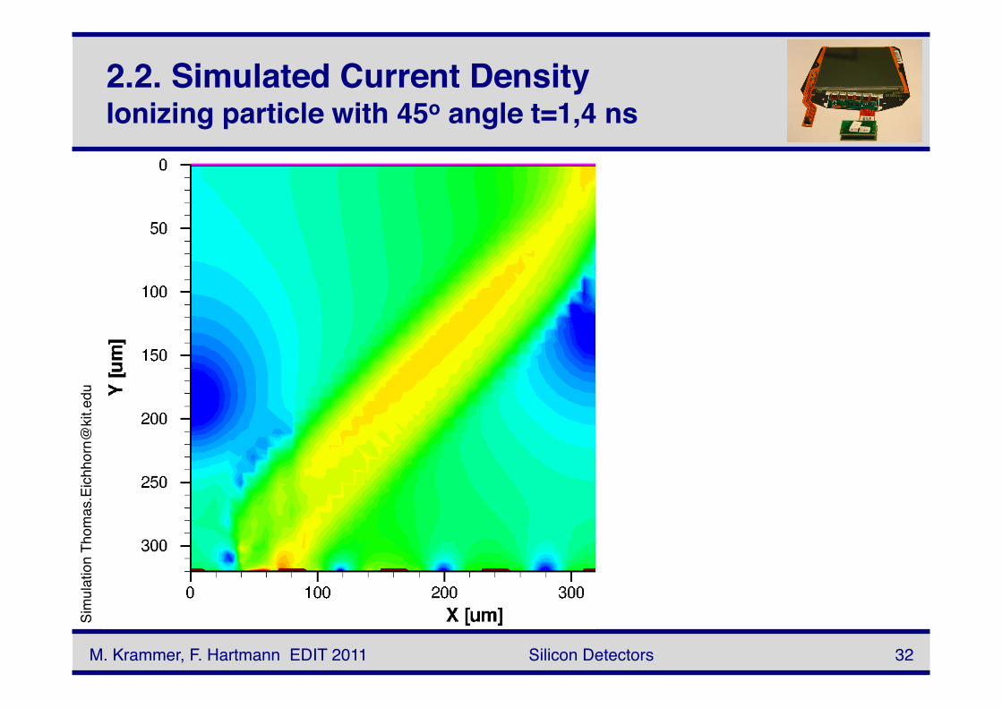
2.2. Simulated Current Density Ionizing particle with 45o angle t=1,4 ns!
Silicon Detectors! 33!
Sim
ulat
ion
Thom
as.E
ichh
orn@
kit.e
du!
M. Krammer, F. Hartmann EDIT 2011!
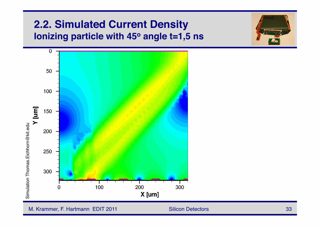
2.2. Simulated Current Density Ionizing particle with 45o angle t=1,5 ns!
Silicon Detectors! 34!
Sim
ulat
ion
Thom
as.E
ichh
orn@
kit.e
du!
M. Krammer, F. Hartmann EDIT 2011!
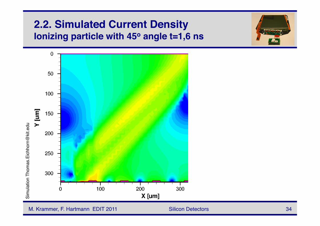
2.2. Simulated Current Density Ionizing particle with 45o angle t=1,6 ns!

Silicon Detectors! 35!
Sim
ulat
ion
Thom
as.E
ichh
orn@
kit.e
du!
M. Krammer, F. Hartmann EDIT 2011!
2.2. Simulated Current Density Ionizing particle with 45o angle t=1,7 ns!
Silicon Detectors! 36!
Sim
ulat
ion
Thom
as.E
ichh
orn@
kit.e
du!
M. Krammer, F. Hartmann EDIT 2011!
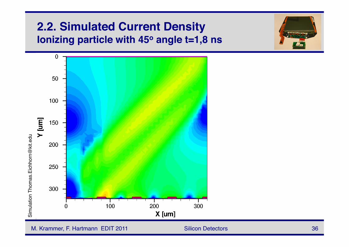
2.2. Simulated Current Density Ionizing particle with 45o angle t=1,8 ns!
Silicon Detectors! 37!
Sim
ulat
ion
Thom
as.E
ichh
orn@
kit.e
du!
M. Krammer, F. Hartmann EDIT 2011!
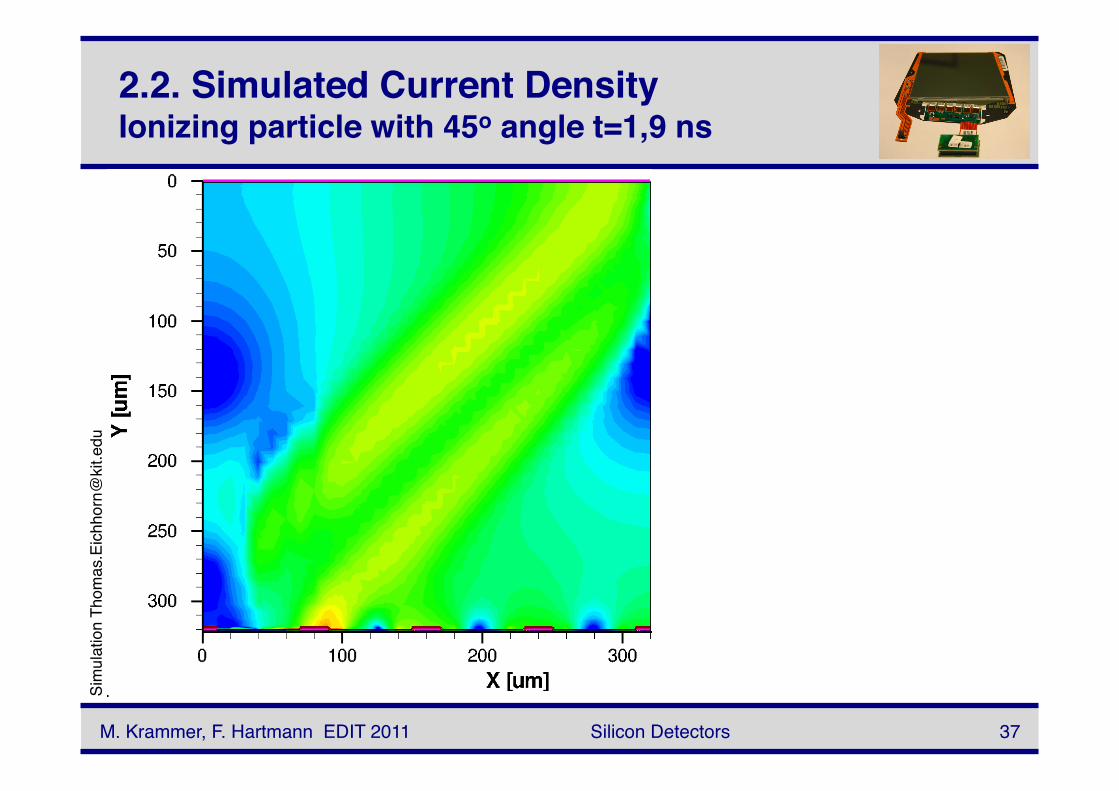
2.2. Simulated Current Density Ionizing particle with 45o angle t=1,9 ns!
Silicon Detectors! 38!
Sim
ulat
ion
Thom
as.E
ichh
orn@
kit.e
du!
M. Krammer, F. Hartmann EDIT 2011!
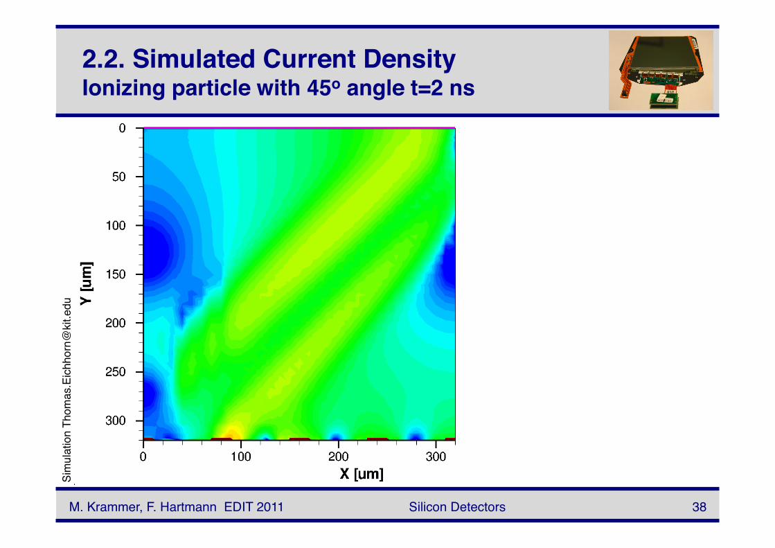
2.2. Simulated Current Density Ionizing particle with 45o angle t=2 ns!
Silicon Detectors! 39!
Sim
ulat
ion
Thom
as.E
ichh
orn@
kit.e
du!
M. Krammer, F. Hartmann EDIT 2011!
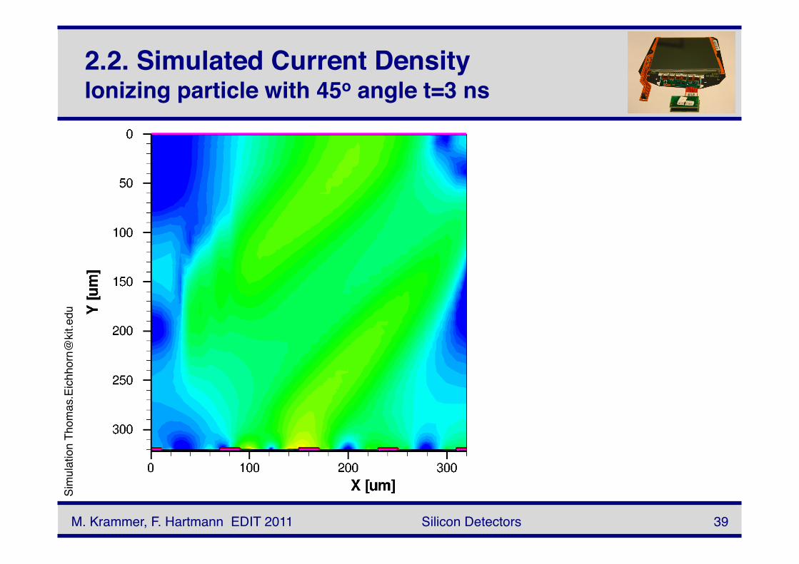
2.2. Simulated Current Density Ionizing particle with 45o angle t=3 ns!
Silicon Detectors! 40!
Sim
ulat
ion
Thom
as.E
ichh
orn@
kit.e
du!
M. Krammer, F. Hartmann EDIT 2011!
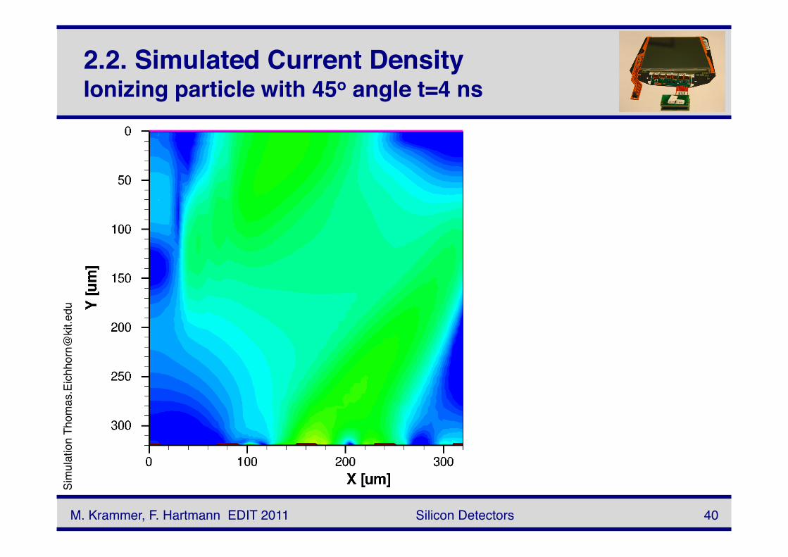
2.2. Simulated Current Density Ionizing particle with 45o angle t=4 ns!
Silicon Detectors! 41!
Sim
ulat
ion
Thom
as.E
ichh
orn@
kit.e
du!
M. Krammer, F. Hartmann EDIT 2011!
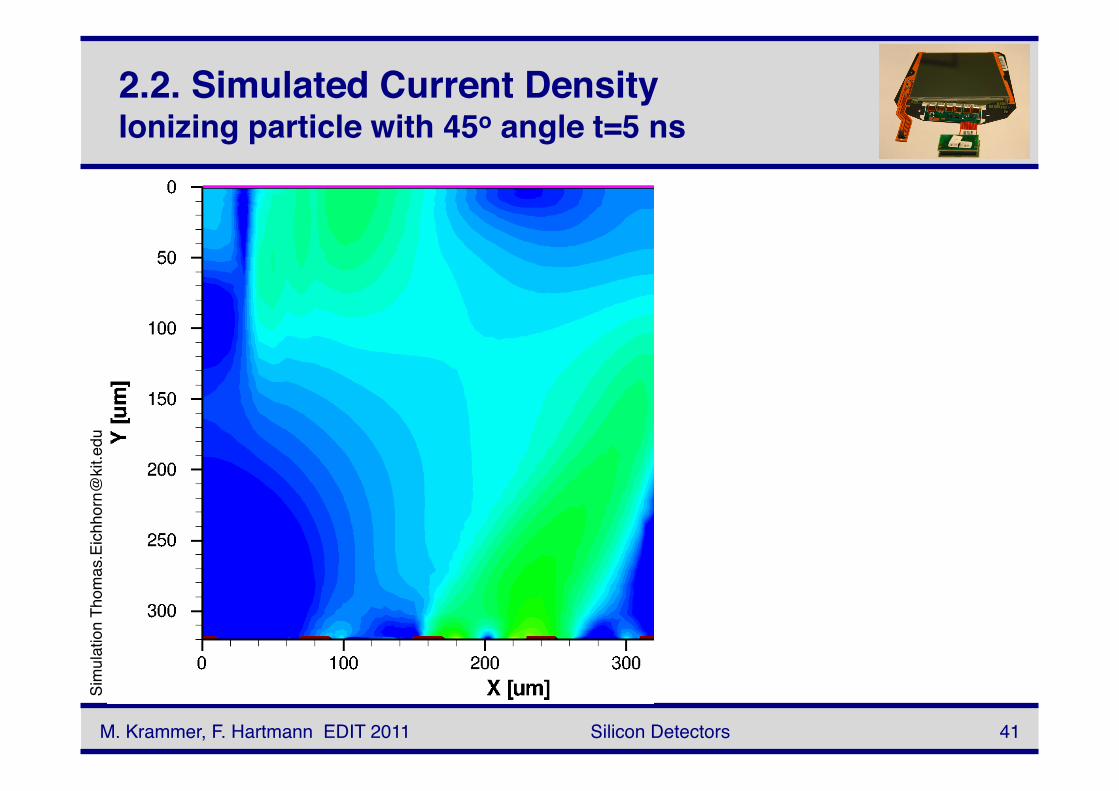
2.2. Simulated Current Density Ionizing particle with 45o angle t=5 ns!
Silicon Detectors! 42!
Sim
ulat
ion
Thom
as.E
ichh
orn@
kit.e
du!
M. Krammer, F. Hartmann EDIT 2011!
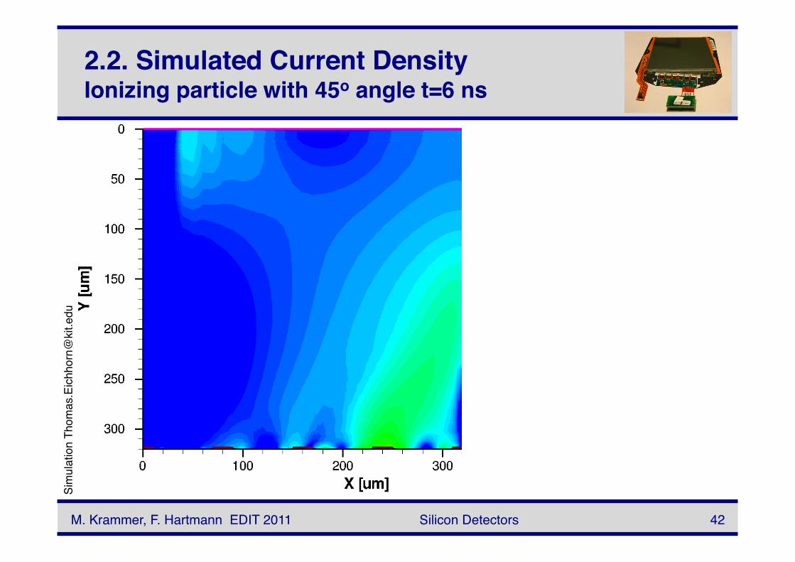
2.2. Simulated Current Density Ionizing particle with 45o angle t=6 ns!
Silicon Detectors! 43!
Sim
ulat
ion
Thom
as.E
ichh
orn@
kit.e
du!
M. Krammer, F. Hartmann EDIT 2011!
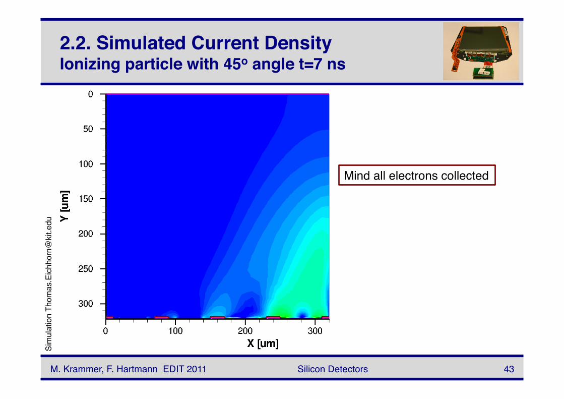
2.2. Simulated Current Density Ionizing particle with 45o angle t=7 ns!
Mind all electrons collected!

2.2. Hole Charge Collection (strip & time resolved)!
Silicon Detectors! 44!
2,27e-15C!
3,27e-15C!
3,04e-15C!
1,08e-15C!
Sim
ulat
ion
Thom
as.E
ichh
orn@
kit.e
du!
M. Krammer, F. Hartmann EDIT 2011!
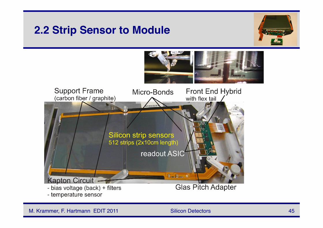
2.2 Strip Sensor to Module!
Silicon Detectors! 45!M. Krammer, F. Hartmann EDIT 2011!
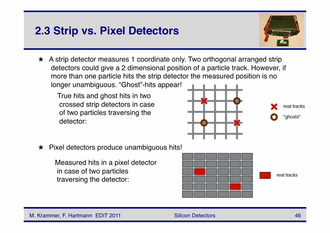
2.3 Strip vs. Pixel Detectors !
Silicon Detectors! 46!
★ A strip detector measures 1 coordinate only. Two orthogonal arranged strip detectors could give a 2 dimensional position of a particle track. However, if more than one particle hits the strip detector the measured position is no longer unambiguous. “Ghost”-hits appear! !
★ Pixel detectors produce unambiguous hits! !
True hits and ghost hits in two crossed strip detectors in case of two particles traversing the detector:!
Measured hits in a pixel detector in case of two particles traversing the detector:!
M. Krammer, F. Hartmann EDIT 2011!
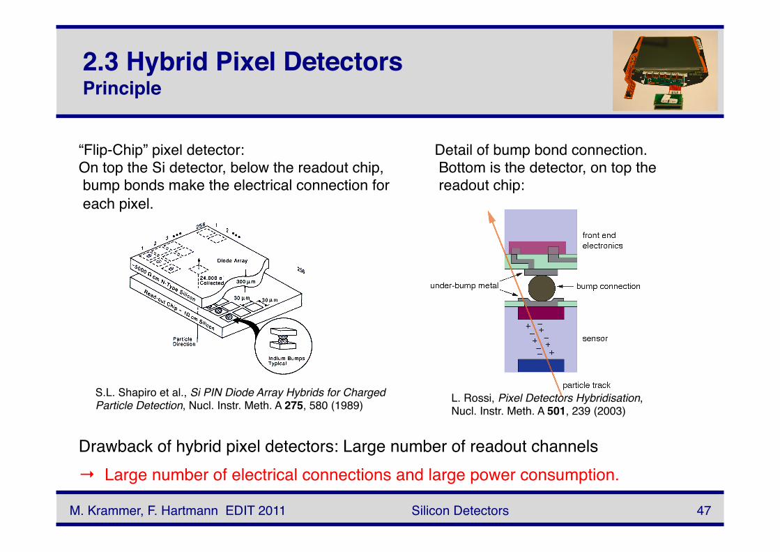
2.3 Hybrid Pixel Detectors Principle!
Silicon Detectors! 47!
Detail of bump bond connection. Bottom is the detector, on top the readout chip:!
“Flip-Chip” pixel detector:!On top the Si detector, below the readout chip, bump bonds make the electrical connection for each pixel. !
S.L. Shapiro et al., Si PIN Diode Array Hybrids for Charged !Particle Detection, Nucl. Instr. Meth. A 275, 580 (1989)! L. Rossi, Pixel Detectors Hybridisation, !
Nucl. Instr. Meth. A 501, 239 (2003)!
Drawback of hybrid pixel detectors: Large number of readout channels!→ Large number of electrical connections and large power consumption.!
M. Krammer, F. Hartmann EDIT 2011!
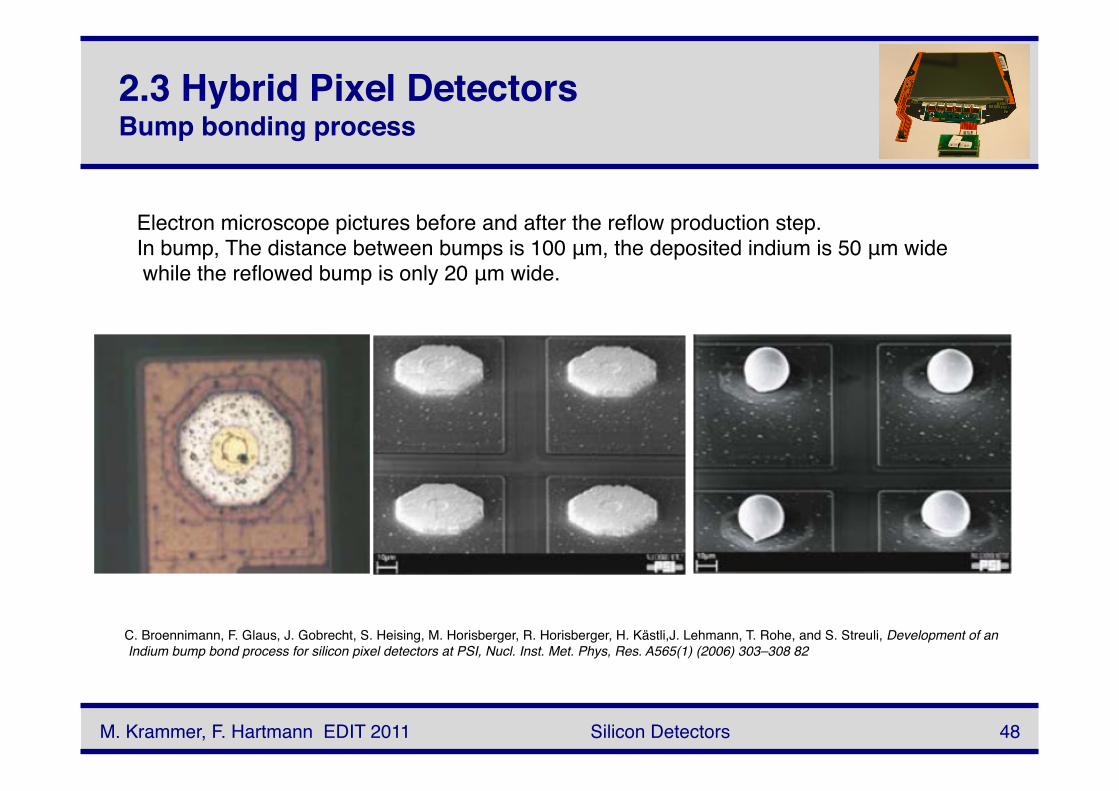
2.3 Hybrid Pixel Detectors Bump bonding process !
Silicon Detectors! 48!
Electron microscope pictures before and after the reflow production step. !In bump, The distance between bumps is 100 μm, the deposited indium is 50 μm wide while the reflowed bump is only 20 μm wide.!
M. Krammer, F. Hartmann EDIT 2011!
C. Broennimann, F. Glaus, J. Gobrecht, S. Heising, M. Horisberger, R. Horisberger, H. Kästli,J. Lehmann, T. Rohe, and S. Streuli, Development of an Indium bump bond process for silicon pixel detectors at PSI, Nucl. Inst. Met. Phys, Res. A565(1) (2006) 303–308 82!
Silicon Detectors! 49!
3 Performance!
M. Krammer, F. Hartmann EDIT 2011!
3.1 Signal to Noise Ratio Introduction!
Silicon Detectors! 50!
The signal generated in a silicon detector depends essentially only! on the thickness of the depletion zone and on the dE/dx of the ! particle.!
The noise in a silicon detector system depends on various ! parameters: geometry of the detector, the biasing scheme, the ! readout electronics, etc. !
!Noise is typically given as “equivalent noise charge” ENC. This !is the noise at the input of the amplifier in elementary charges. !
M. Krammer, F. Hartmann EDIT 2011!
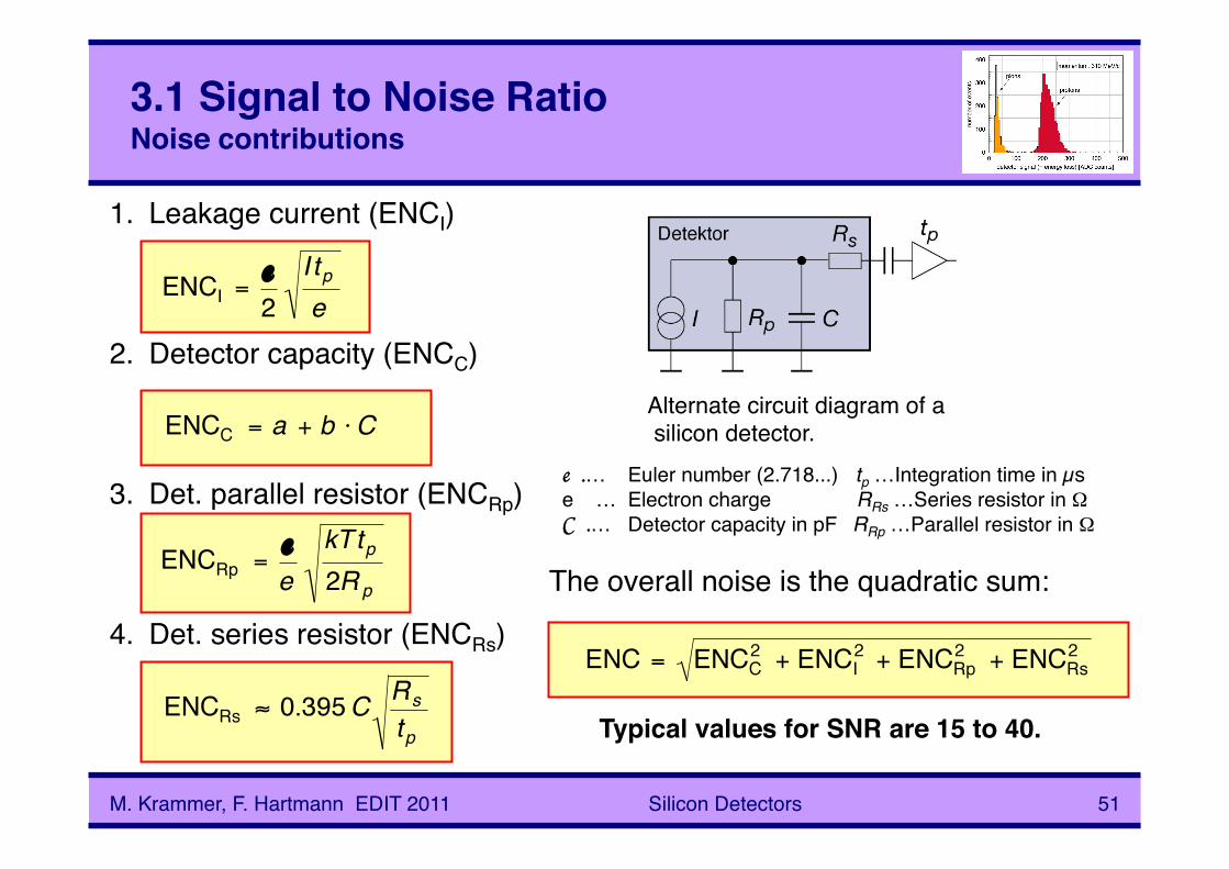
3.1 Signal to Noise Ratio Noise contributions!
Silicon Detectors! 51!
1. Leakage current (ENCI)!
2. Detector capacity (ENCC)!
3. Det. parallel resistor (ENCRp)!
4. Det. series resistor (ENCRs)!
The overall noise is the quadratic sum:!
Alternate circuit diagram of a silicon detector. !
M. Krammer, F. Hartmann EDIT 2011!
e .… !Euler number (2.718...) tp …Integration time in µs e !… !Electron charge RRs …Series resistor in Ω !C .… !Detector capacity in pF RRp …Parallel resistor in Ω
Typical values for SNR are 15 to 40.!
€
ENCI =e2
I tpe
€
ENCRp =ee
kTtp2Rp
3.2 Position ResolutionIntroduction!
Silicon Detectors! 52!
★ Physics processes:!– Statistical fluctuations of the energy loss!– Diffusion of charge carriers!
★ External parameter:!– Binary readout (thresh hold counter) or read out of
analogue signal value!– Distance between strips (strip pitch)!– Signal to noise ratio!
The position resolution – the main parameter of a position detector – depends on various factors, some due to physics constraints and some due to the design of the system (external parameters). !
M. Krammer, F. Hartmann EDIT 2011!
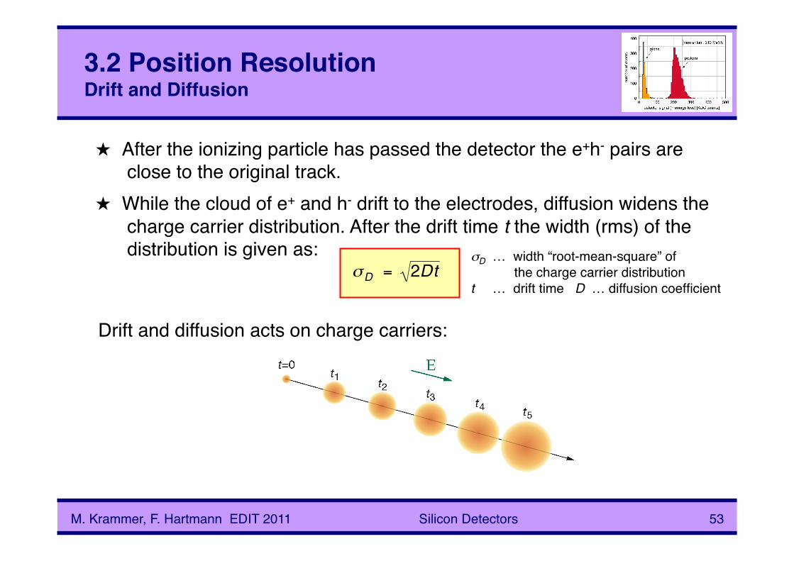
3.2 Position ResolutionDrift and Diffusion!
Silicon Detectors! 53!
★ After the ionizing particle has passed the detector the e+h- pairs are close to the original track. !
★ While the cloud of e+ and h- drift to the electrodes, diffusion widens the charge carrier distribution. After the drift time t the width (rms) of the distribution is given as:! σD !… !width “root-mean-square” of !
! ! the charge carrier distribution!t !… !drift time D … diffusion coefficient!
Drift and diffusion acts on charge carriers:!
M. Krammer, F. Hartmann EDIT 2011!
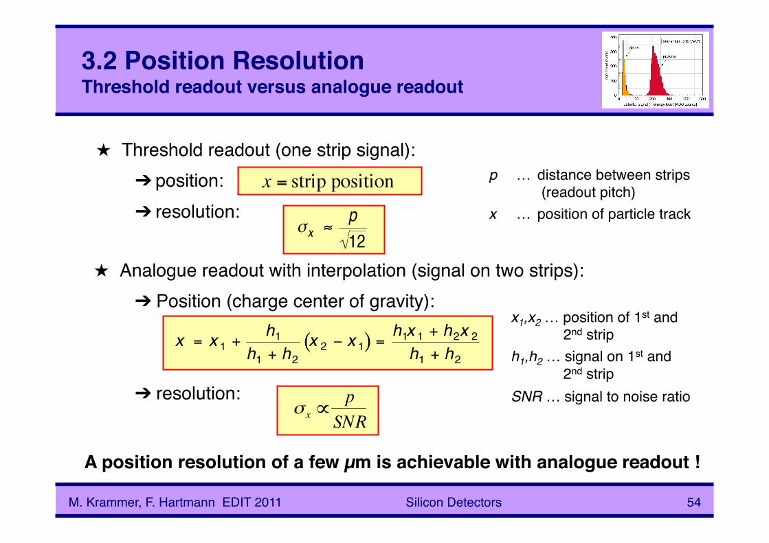
3.2 Position ResolutionThreshold readout versus analogue readout!
Silicon Detectors! 54!
★ Analogue readout with interpolation (signal on two strips):!➔ Position (charge center of gravity): !
➔ resolution: !
p !… !distance between strips (readout pitch)!
x !… !position of particle track!
★ Threshold readout (one strip signal):!➔ position:!➔ resolution: !
x1,x2 … position of 1st and 2nd strip!
h1,h2 … signal on 1st and 2nd strip!
SNR … signal to noise ratio!
A position resolution of a few µm is achievable with analogue readout !!
M. Krammer, F. Hartmann EDIT 2011!
Silicon Detectors! 55!
4 Detector Systems!
M. Krammer, F. Hartmann EDIT 2011!
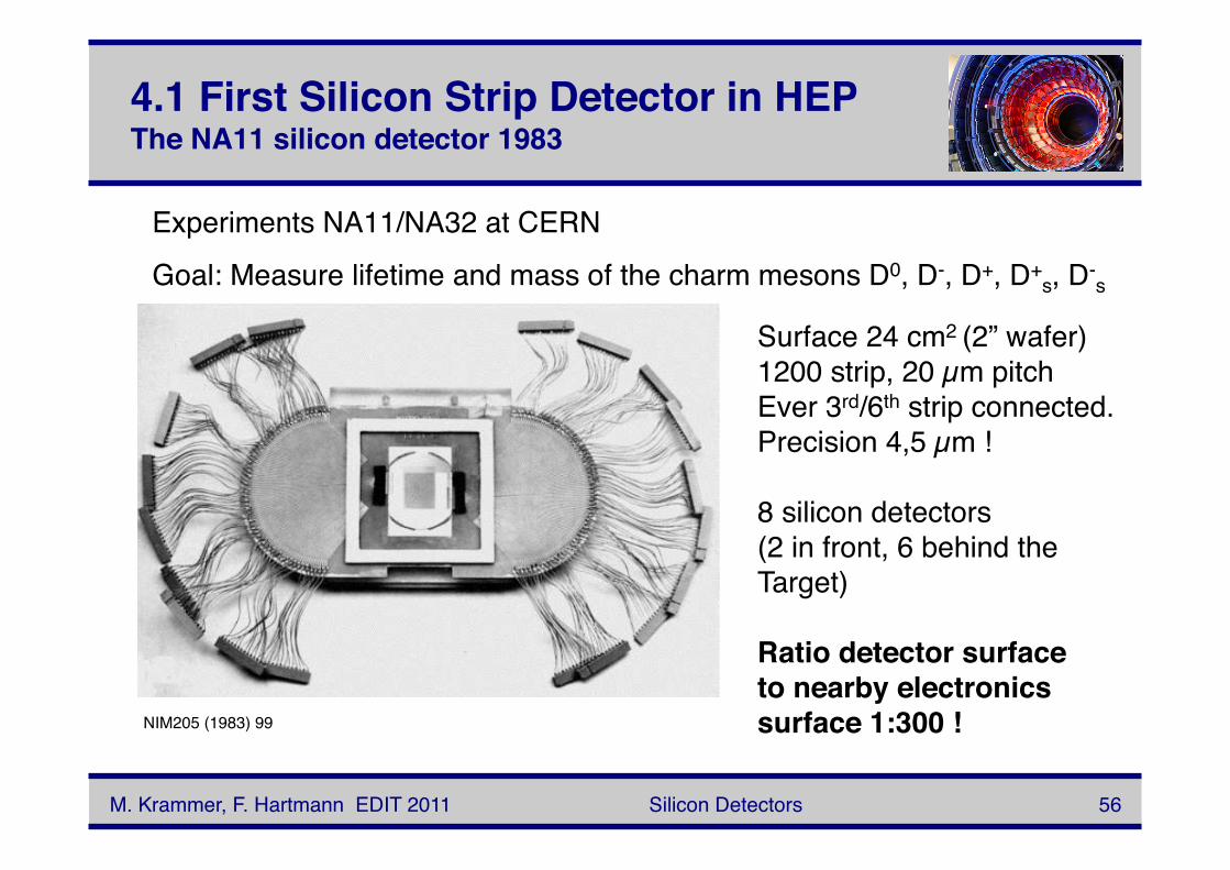
4.1 First Silicon Strip Detector in HEP The NA11 silicon detector 1983!
Silicon Detectors! 56!
Experiments NA11/NA32 at CERN !
Goal: Measure lifetime and mass of the charm mesons D0, D-, D+, D+s, D-
s!
Surface 24 cm2 (2” wafer)!1200 strip, 20 µm pitch!Ever 3rd/6th strip connected.!Precision 4,5 µm !!
8 silicon detectors!(2 in front, 6 behind the!Target)!
Ratio detector surface !to nearby electronics!surface 1:300 !!NIM205 (1983) 99!
M. Krammer, F. Hartmann EDIT 2011!
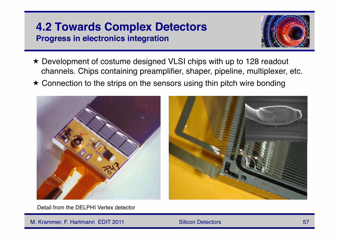
4.2 Towards Complex Detectors Progress in electronics integration!
Silicon Detectors! 57!
Development of costume designed VLSI chips with up to 128 readout ! channels. Chips containing preamplifier, shaper, pipeline, multiplexer, etc.! Connection to the strips on the sensors using thin pitch wire bonding!
Detail from the DELPHI Vertex detector!
M. Krammer, F. Hartmann EDIT 2011!
4.3 Silicon Trackers at the LHC!
Silicon Detectors! 58!
25 years and many developments later: !
! ! !!
! !Silicon Trackers in the LHC !Experiments!
M. Krammer, F. Hartmann EDIT 2011!
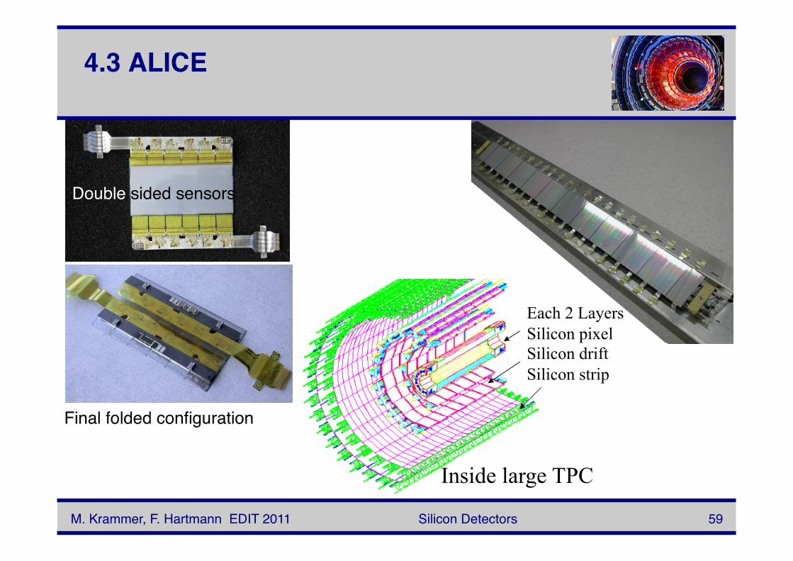
4.3 ALICE
Silicon Detectors! 59!
Each 2 Layers Silicon pixel Silicon drift Silicon strip
Inside large TPC
Final folded configuration!
Double sided sensors!
M. Krammer, F. Hartmann EDIT 2011!
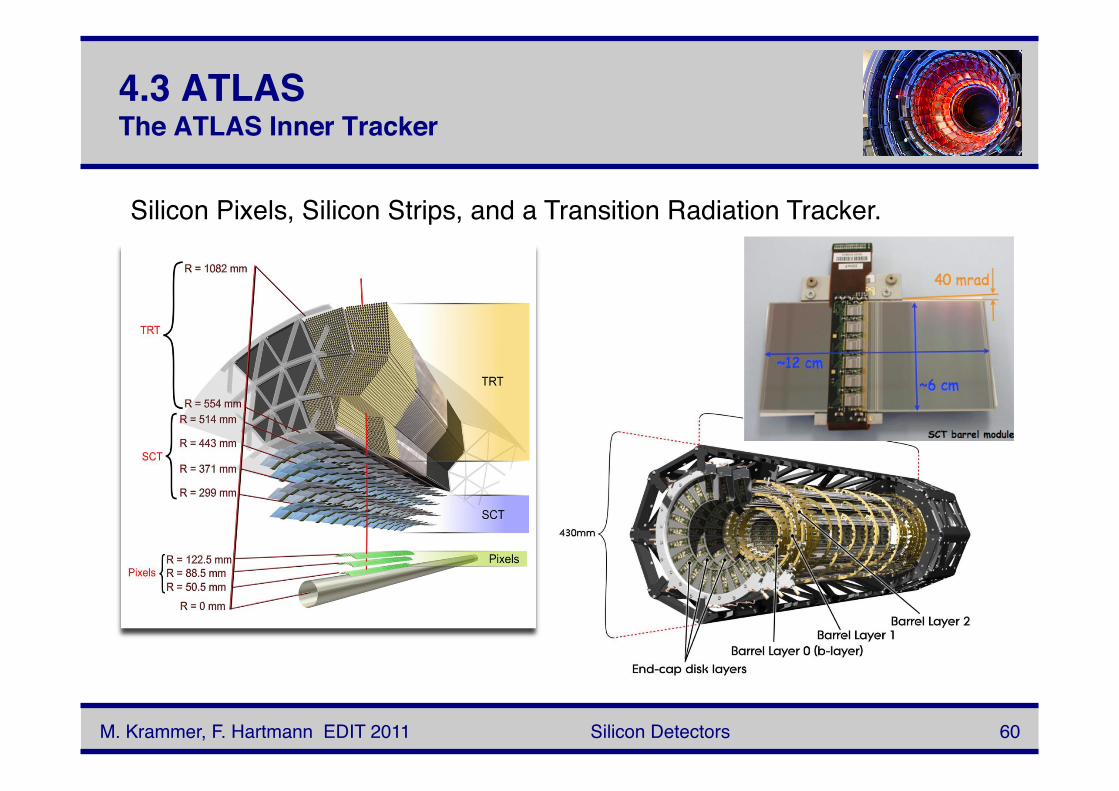
4.3 ATLASThe ATLAS Inner Tracker!
Silicon Detectors! 60!
Silicon Pixels, Silicon Strips, and a Transition Radiation Tracker.!
M. Krammer, F. Hartmann EDIT 2011!
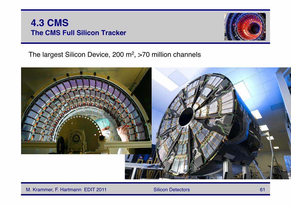
4.3 CMS The CMS Full Silicon Tracker!
Silicon Detectors! 61!
The largest Silicon Device, 200 m2, >70 million channels!
M. Krammer, F. Hartmann EDIT 2011!

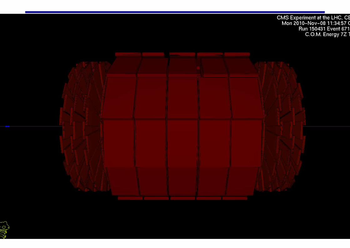
Tracker Insertion!
M. Krammer, F. Hartmann EDIT 2011! Silicon Detectors! 62!
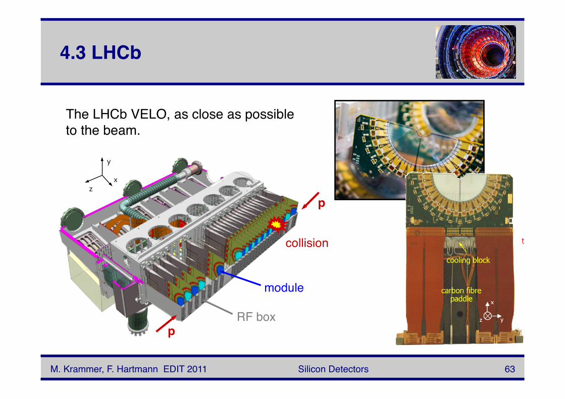
4.3 LHCb!
Silicon Detectors! 63!
RF box!
module!
z x
y
p!
p!
collision!
The LHCb VELO, as close as possible!to the beam.!
M. Krammer, F. Hartmann EDIT 2011!
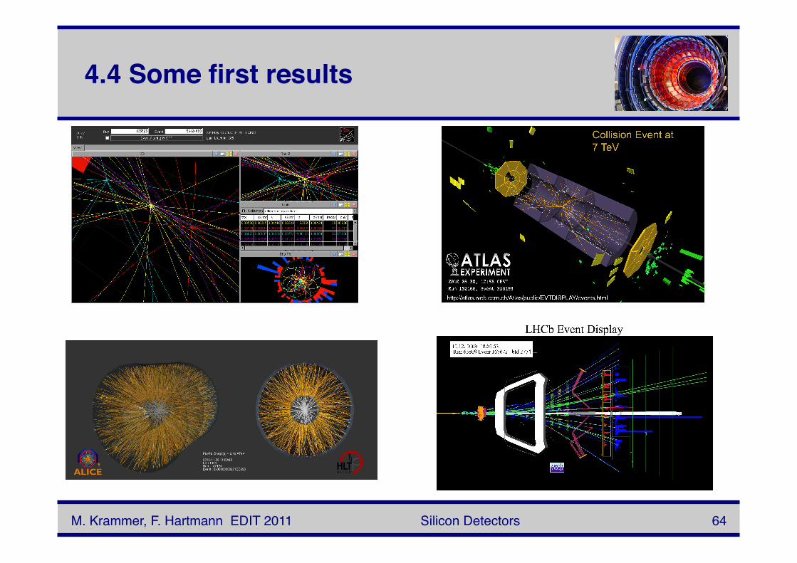
4.4 Some first results!
Silicon Detectors! 64!M. Krammer, F. Hartmann EDIT 2011!
Silicon Detectors! 65!M. Krammer, F. Hartmann EDIT 2011!
Silicon Detectors! 66!
! !THE END !
of this lecture, but not the end of !silicon sensor developments for !experiments in high energy physics.!
M. Krammer, F. Hartmann EDIT 2011!
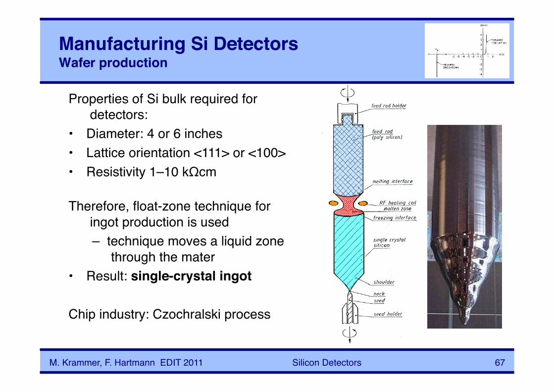
Manufacturing Si Detectors Wafer production!
M. Krammer, F. Hartmann EDIT 2011! Silicon Detectors! 67!
Properties of Si bulk required for detectors:!
• Diameter: 4 or 6 inches !• Lattice orientation <111> or <100>!• Resistivity 1–10 kΩcm
Therefore, float-zone technique for ingot production is used!– technique moves a liquid zone
through the mater!• Result: single-crystal ingot!
Chip industry: Czochralski process!
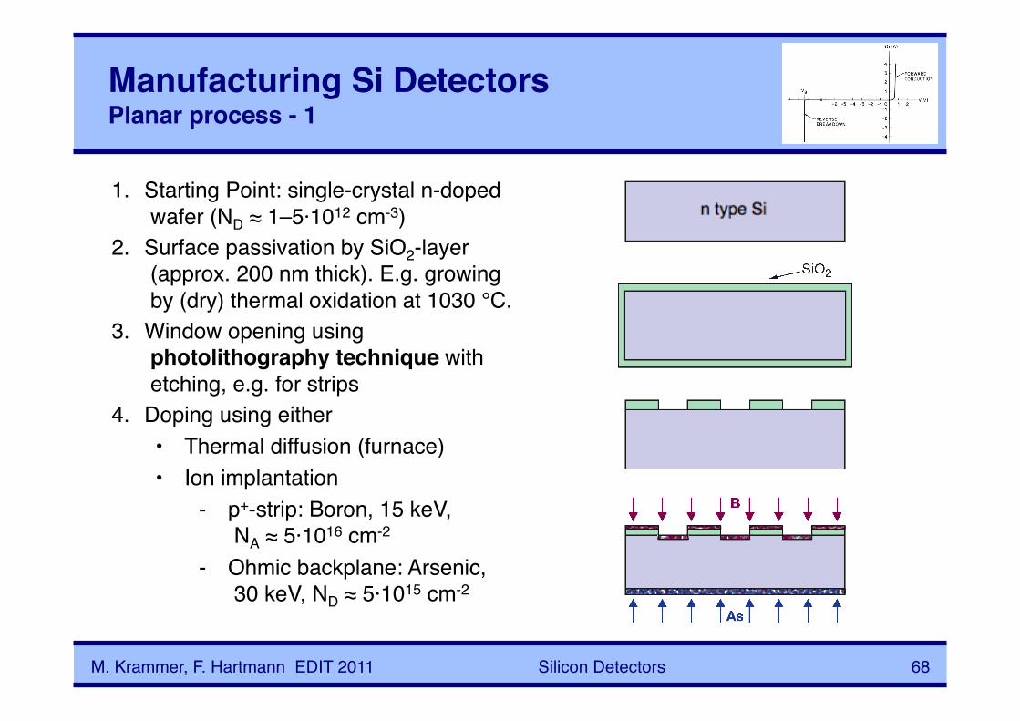
Manufacturing Si Detectors Planar process - 1 !
M. Krammer, F. Hartmann EDIT 2011! Silicon Detectors! 68!
1. Starting Point: single-crystal n-doped wafer (ND ≈ 1–5·1012 cm-3)!
2. Surface passivation by SiO2-layer (approx. 200 nm thick). E.g. growing by (dry) thermal oxidation at 1030 °C.!
3. Window opening using photolithography technique with etching, e.g. for strips!
4. !Doping using either !• Thermal diffusion (furnace)!• Ion implantation!
- p+-strip: Boron, 15 keV, NA ≈ 5·1016 cm-2!
- Ohmic backplane: Arsenic, 30 keV, ND ≈ 5·1015 cm-2!

Manufacturing Si Detectors Planar process - 2!
M. Krammer, F. Hartmann EDIT 2011! Silicon Detectors! 69!
5. After ion implantation: Curing of damage via thermal annealing at approx. 600°C, (activation of dopant atoms by incorporation into silicon lattice)!
6. Metallization of front side: sputtering or CVD!
7. Removing of excess metal by photolitography: etching of non-covered areas!
8. Full-area metallization of backplane with annealing at approx. 450°C for better adherence between metal and silicon
Last step: wafer dicing (cutting)!
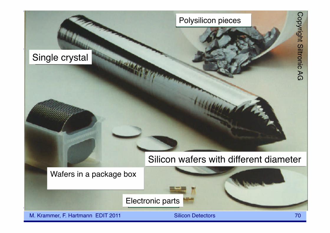
2.6 Manufacturing Si Detectors
M. Krammer, F. Hartmann EDIT 2011! Silicon Detectors! 70!
Single crystal!
Polysilicon pieces!
Silicon wafers with different diameter!
Electronic parts!
Wafers in a package box!
Copyright Siltronic AG
!