Tetsuo ABE - CERN Indico
39
Status of Quadrant - type Waveguide - damped Structure Fabrication and Single - Cell SW Cavity Test Tetsuo ABE <[email protected]> High Energy Accelerator Research Organization (KEK), Japan CLIC Workshop 2019 @ CERN 2019-01-21
-
Upload
khangminh22 -
Category
Documents
-
view
0 -
download
0
Transcript of Tetsuo ABE - CERN Indico
Status of
Quadrant-type Waveguide-
damped Structure Fabrication
and Single-Cell SW Cavity Test
Tetsuo ABE<[email protected]>
High Energy Accelerator Research Organization (KEK), Japan
CLIC Workshop 2019 @ CERN
2019-01-21
Tetsuo ABE (KEK)
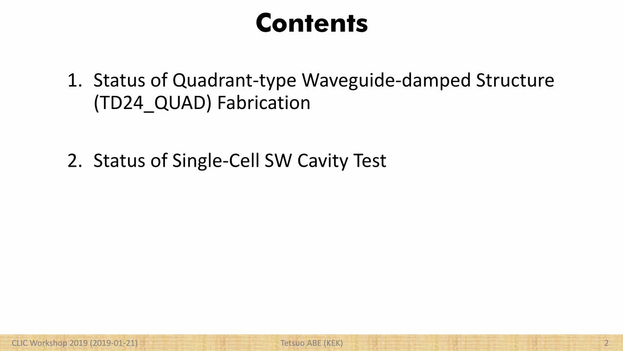
Contents
1. Status of Quadrant-type Waveguide-damped Structure (TD24_QUAD) Fabrication
2. Status of Single-Cell SW Cavity Test
CLIC Workshop 2019 (2019-01-21) 2
Tetsuo ABE (KEK) 3CLIC Workshop 2019 (2019-01-21)
Tetsuo ABE (KEK) 4CLIC Workshop 2019 (2019-01-21)
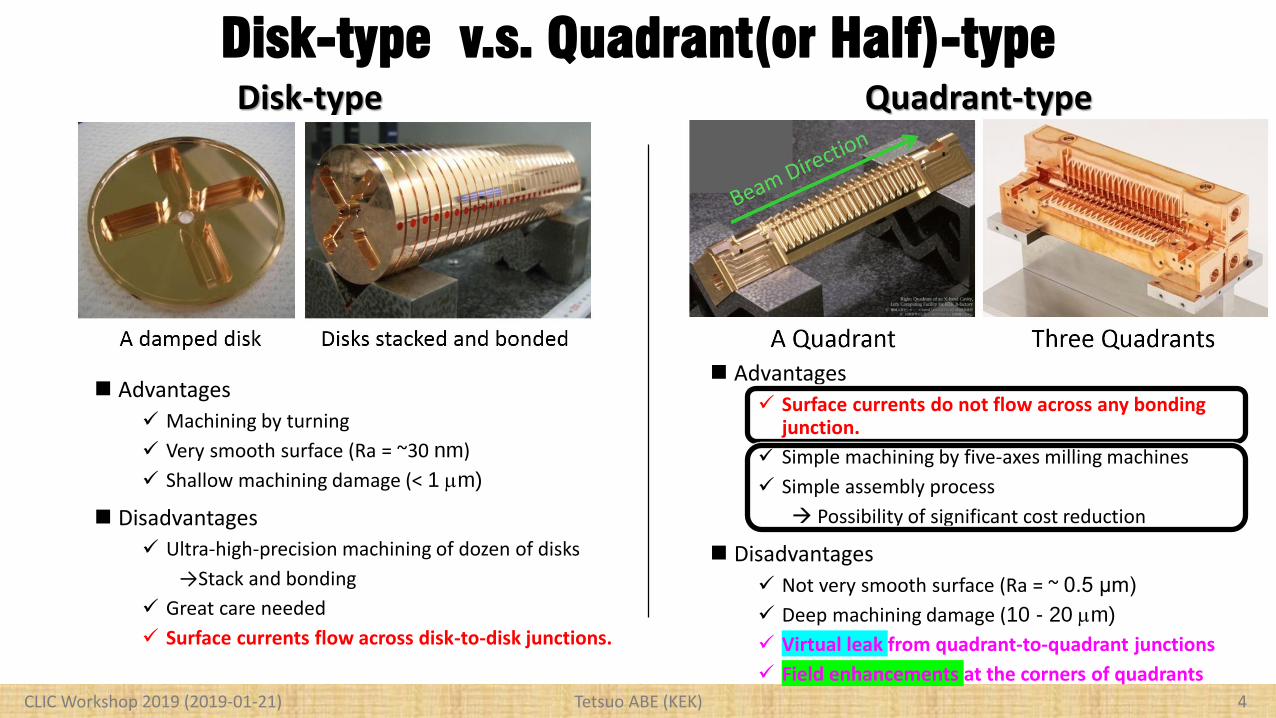
Disk-type v.s. Quadrant(or Half)-type
Advantages
Machining by turning
Very smooth surface (Ra = ~30 nm)
Shallow machining damage (< 1 mm)
Disadvantages
Ultra-high-precision machining of dozen of disks
→Stack and bonding
Great care needed
Surface currents flow across disk-to-disk junctions.
Disk-type Quadrant-type
Advantages
Surface currents do not flow across any bonding junction.
Simple machining by five-axes milling machines
Simple assembly process
Possibility of significant cost reduction
Disadvantages
Not very smooth surface (Ra = ~ 0.5 μm)
Deep machining damage (10 - 20 mm)
Virtual leak from quadrant-to-quadrant junctions
Field enhancements at the corners of quadrants

Tetsuo ABE (KEK) 5
Design improvement
CLIC Workshop 2019 (2019-01-21)
FlatContact
Quadrant A
Quadrant B
8×R50μm
Large R(8×R0.4mm)
Small Gap(0.1mm)
Old Design( Bad performance)
Improved Design
Avoid virtual leak Suppress the field enhancement
The chamfer radius and small-gap size were optimized based on simulation to minimize
A) Field enhancement at the corner of the quadrants ( +25%)
B) Deterioration of the shunt impedance ( -2%)
For details, see T. Abe et al., “Fabrication of Quadrant-Type X-Band Single-Cell Structure used for High Gradient Tests,”
presented at the 11th Annual Meeting of Particle Accelerator Society of Japan (2014), Paper ID: SUP042.
to
Tetsuo ABE (KEK) 6
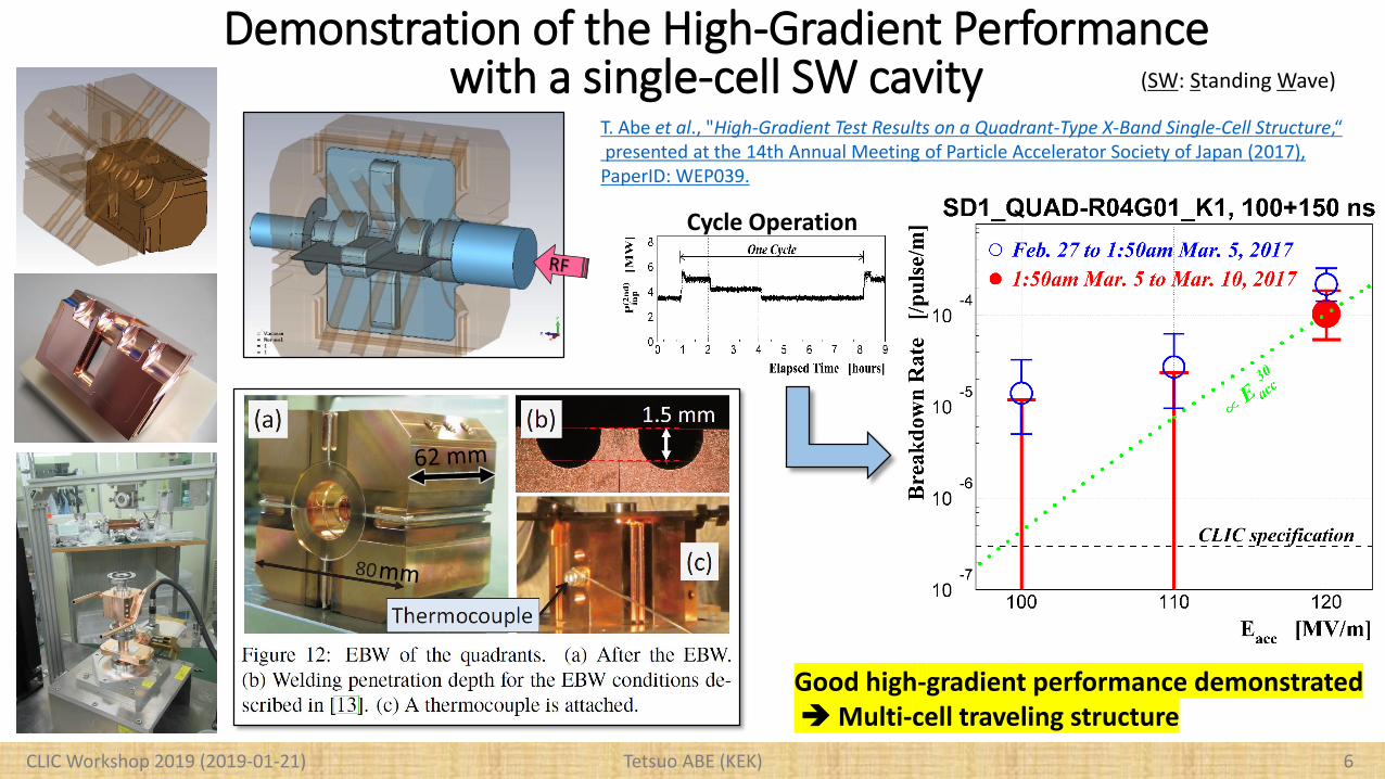
Demonstration of the High-Gradient Performancewith a single-cell SW cavity
CLIC Workshop 2019 (2019-01-21)
Good high-gradient performance demonstratedMulti-cell traveling structure
T. Abe et al., "High-Gradient Test Results on a Quadrant-Type X-Band Single-Cell Structure,“presented at the 14th Annual Meeting of Particle Accelerator Society of Japan (2017), PaperID: WEP039.
(SW: Standing Wave)
Cycle Operation
Tetsuo ABE (KEK) 7CLIC Workshop 2019 (2019-01-21)
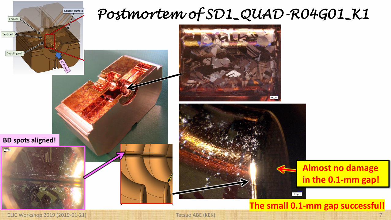
Postmortem of SD1_QUAD-R04G01_K1
Almost no damage in the 0.1-mm gap!
The small 0.1-mm gap successful!
BD spots aligned!
Tetsuo ABE (KEK) 8CLIC Workshop 2019 (2019-01-21)
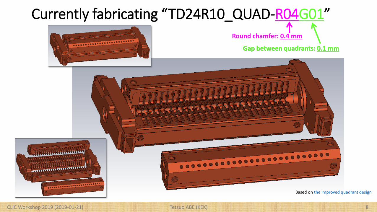
Currently fabricating “TD24R10_QUAD-R04G01”Round chamfer: 0.4 mm
Gap between quadrants: 0.1 mm
Based on the improved quadrant design
Tetsuo ABE (KEK) 9CLIC Workshop 2019 (2019-01-21)
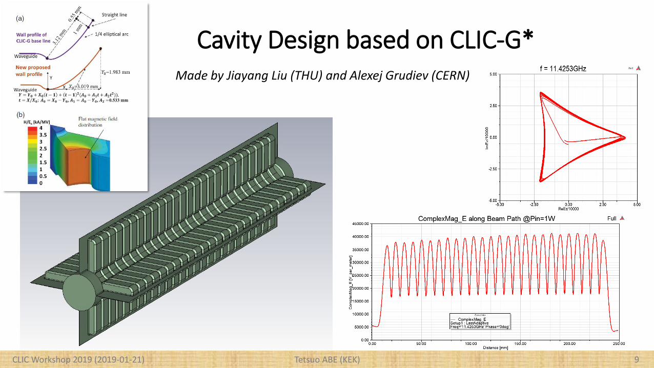
Cavity Design based on CLIC-G*Made by Jiayang Liu (THU) and Alexej Grudiev (CERN)
Tetsuo ABE (KEK) 10
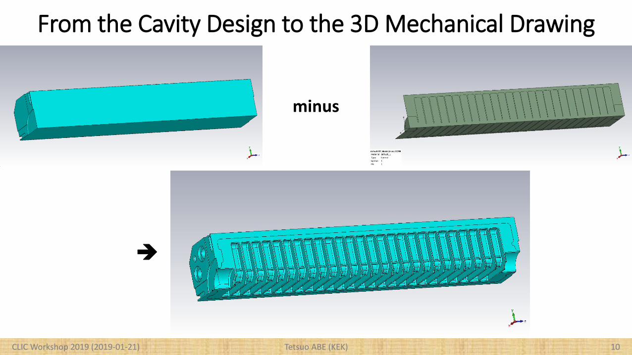
From the Cavity Design to the 3D Mechanical Drawing
CLIC Workshop 2019 (2019-01-21)
minus

Tetsuo ABE (KEK) 11
A Quadrant Machined with Ultraprecision Milling
CLIC Workshop 2019 (2019-01-21)
By U-Corporation
Tetsuo ABE (KEK) 12
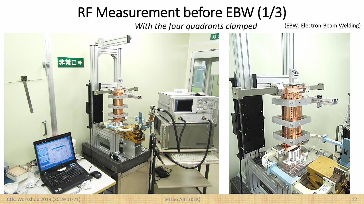
RF Measurement before EBW (1/3)
CLIC Workshop 2019 (2019-01-21)
With the four quadrants clamped (EBW: Electron-Beam Welding)
Tetsuo ABE (KEK) 13CLIC Workshop 2019 (2019-01-21)
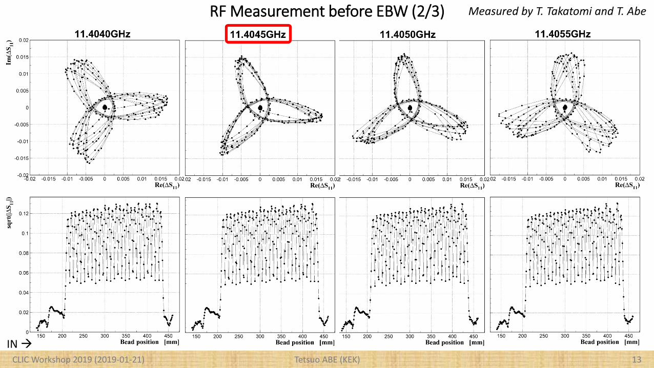
RF Measurement before EBW (2/3) Measured by T. Takatomi and T. Abe
IN
Tetsuo ABE (KEK) 14
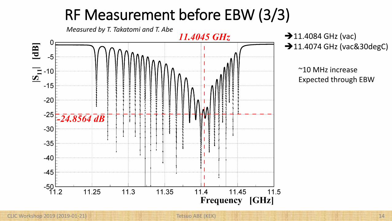
RF Measurement before EBW (3/3)
CLIC Workshop 2019 (2019-01-21)
11.4084 GHz (vac) 11.4074 GHz (vac&30degC)
~10 MHz increaseExpected through EBW
Measured by T. Takatomi and T. Abe
Tetsuo ABE (KEK) 15
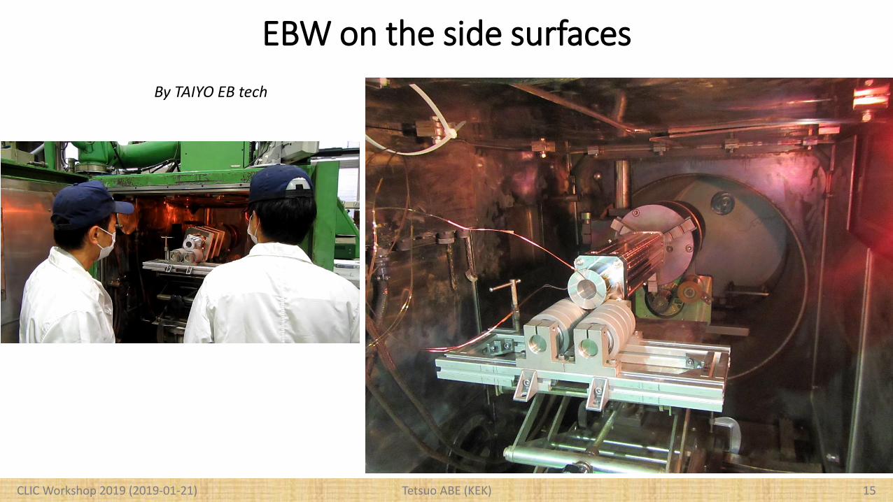
EBW on the side surfaces
CLIC Workshop 2019 (2019-01-21)
By TAIYO EB tech
Tetsuo ABE (KEK) 16
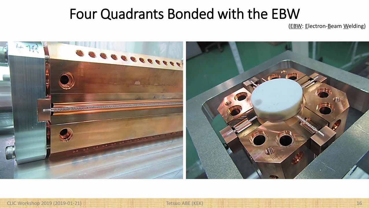
Four Quadrants Bonded with the EBW
CLIC Workshop 2019 (2019-01-21)
(EBW: Electron-Beam Welding)

Tetsuo ABE (KEK) 17
RF Measurement after the EBW
CLIC Workshop 2019 (2019-01-21)
IN OUT
Measured by T. Takatomi and T. Abe
Tetsuo ABE (KEK) 18
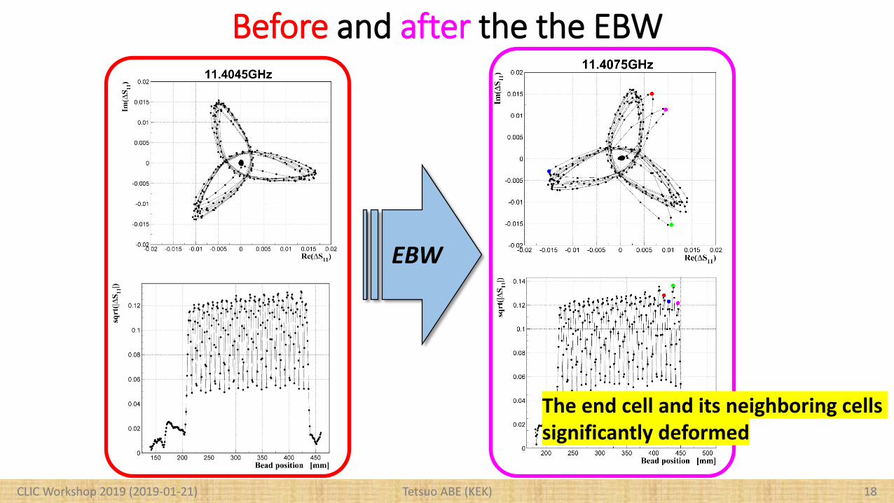
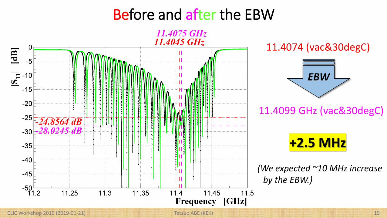
Before and after the the EBW
CLIC Workshop 2019 (2019-01-21)
EBW
The end cell and its neighboring cells significantly deformed
Tetsuo ABE (KEK) 19
Before and after the EBW
CLIC Workshop 2019 (2019-01-21)
11.4074 (vac&30degC)
11.4099 GHz (vac&30degC)
EBW
+2.5 MHz
(We expected ~10 MHz increase by the EBW.)
Tetsuo ABE (KEK) 20
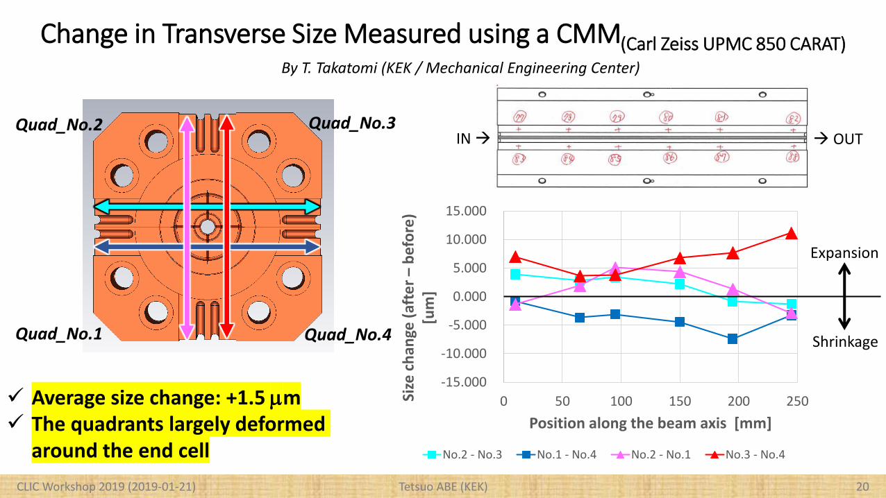
Change in Transverse Size Measured using a CMM(Carl Zeiss UPMC 850 CARAT)
CLIC Workshop 2019 (2019-01-21)
Quad_No.1
Quad_No.2 Quad_No.3
Quad_No.4
-15.000
-10.000
-5.000
0.000
5.000
10.000
15.000
0 50 100 150 200 250Size
ch
ange
(af
ter –
be
fore
) [u
m]
Position along the beam axis [mm]
No.2 - No.3 No.1 - No.4 No.2 - No.1 No.3 - No.4
By T. Takatomi (KEK / Mechanical Engineering Center)
Average size change: +1.5 mm The quadrants largely deformed
around the end cell
Expansion
Shrinkage
IN OUT

Tetsuo ABE (KEK) 21
After brazing tuner pins…
CLIC Workshop 2019 (2019-01-21)
Most of the tuner pins dropped!
Pearskin!
OFC (class1)CuZr
First time to be processed at a high temperature
Alumina ceramics put here
High-temperature-treated copper plates made of CuZr and pure copper (OFC, class1)
Tetsuo ABE (KEK) 22
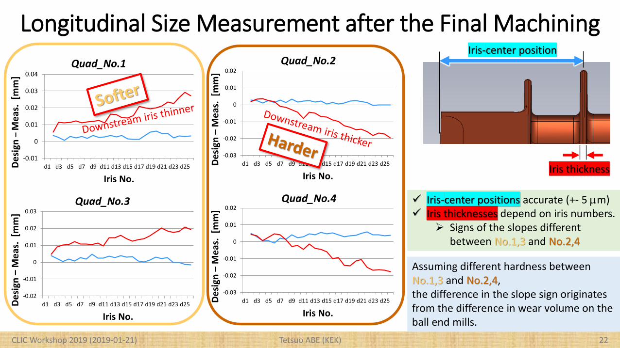
Longitudinal Size Measurement after the Final Machining
CLIC Workshop 2019 (2019-01-21)
-0.01
0
0.01
0.02
0.03
0.04
d1 d3 d5 d7 d9 d11 d13 d15 d17 d19 d21 d23 d25De
sign
–M
eas
. [
mm
]
Iris No.
Quad_No.1
-0.03
-0.02
-0.01
0
0.01
0.02
d1 d3 d5 d7 d9 d11 d13 d15 d17 d19 d21 d23 d25De
sign
–M
eas
. [m
m]
Iris No.
Quad_No.2
-0.02
-0.01
0
0.01
0.02
0.03
d1 d3 d5 d7 d9 d11 d13 d15 d17 d19 d21 d23 d25De
sign
–M
eas
. [m
m]
Iris No.
Quad_No.3
-0.03
-0.02
-0.01
0
0.01
0.02
d1 d3 d5 d7 d9 d11 d13 d15 d17 d19 d21 d23 d25De
sign
–M
eas
. [m
m]
Iris No.
Quad_No.4 Iris-center positions accurate (+- 5 mm) Iris thicknesses depend on iris numbers.
Signs of the slopes different between No.1,3 and No.2,4
Iris-center position
Iris thickness
Assuming different hardness between No.1,3 and No.2,4,the difference in the slope sign originates from the difference in wear volume on the ball end mills.

Tetsuo ABE (KEK) 23CLIC Workshop 2019 (2019-01-21)
Quad_No.1
Quad_No.2
Quad_No.3 Quad_No.4
Softer
Harder
Harder
Softer

Tetsuo ABE (KEK)
Updated Schedule on TD24_QUAD
① Milling of quadrants to be completed by March 2019
② RF & size meas. EBW RF & size meas. by April 2019
③ Brazing of tuner pins, couplers, etc. by May 2019
④ High-gradient test to be started before summer 2019
CLIC Workshop 2019 (2019-01-21) 24
Tetsuo ABE (KEK) 25CLIC Workshop 2019 (2019-01-21)
Tetsuo ABE (KEK) 26
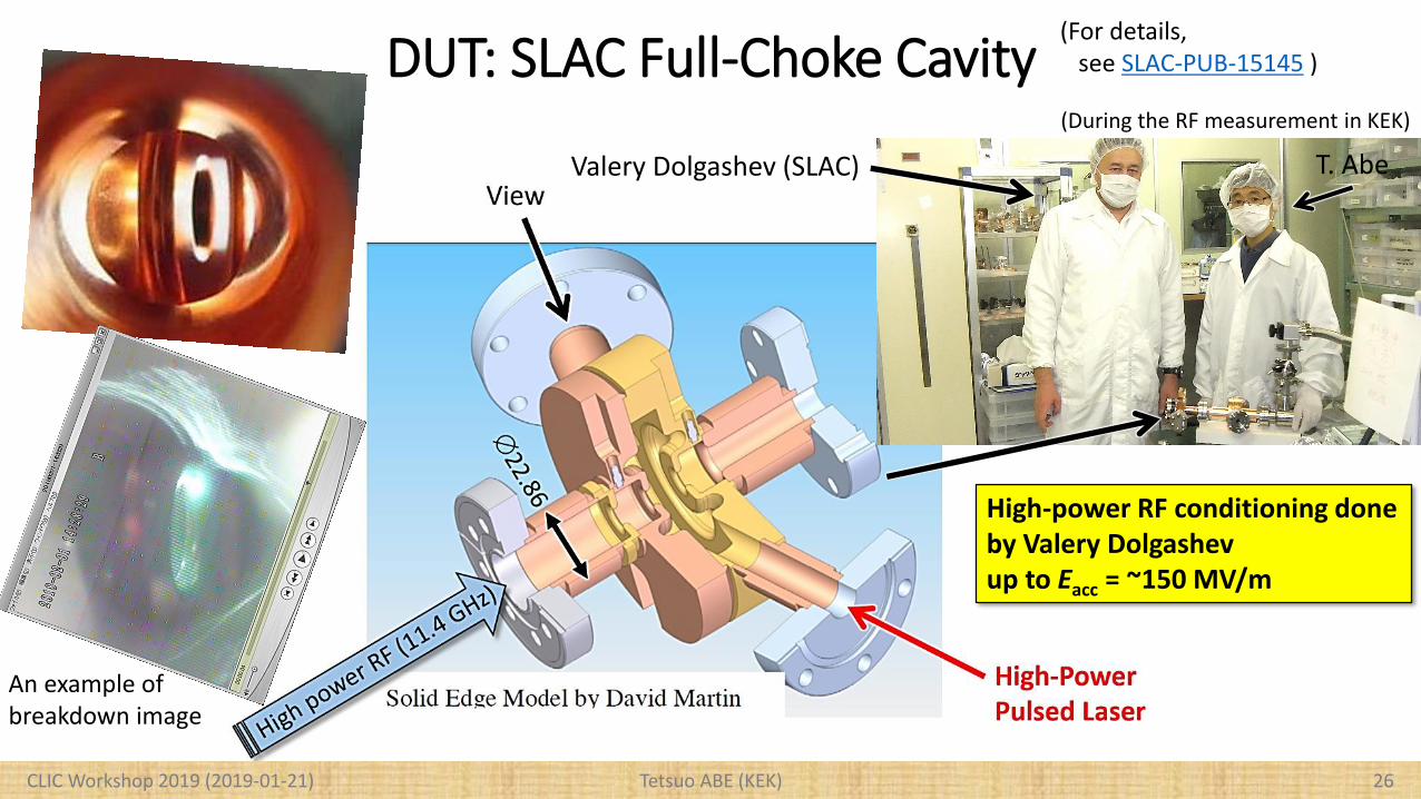
DUT: SLAC Full-Choke Cavity
CLIC Workshop 2019 (2019-01-21)
Valery Dolgashev (SLAC)
An example of breakdown image
High-power RF conditioning doneby Valery Dolgashevup to Eacc = ~150 MV/m
(During the RF measurement in KEK)
(For details, see SLAC-PUB-15145 )
T. Abe
Tetsuo ABE (KEK) 27
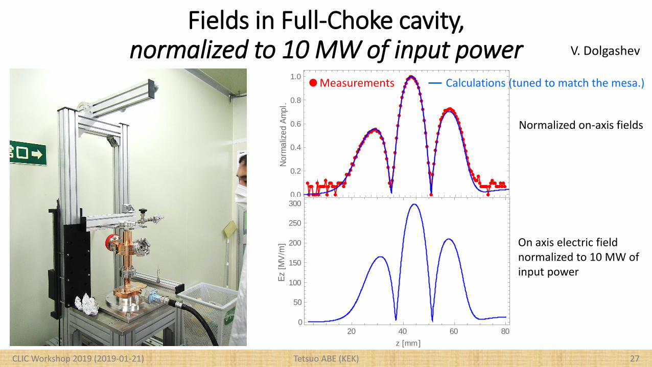
Fields in Full-Choke cavity,normalized to 10 MW of input power
CLIC Workshop 2019 (2019-01-21)
Normalized on-axis fields
10 20 30 40 50 60 700.0
0.2
0.4
0.6
0.8
1.0
z mm
No
rma
lize
dA
mp
l.
20 40 60 800
50
100
150
200
250
300
z mm
Ez
MV
m
On axis electric field normalized to 10 MW of input power
V. Dolgashev
Measurements Calculations (tuned to match the mesa.)
Tetsuo ABE (KEK) 28
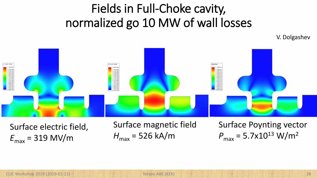
Fields in Full-Choke cavity,normalized go 10 MW of wall losses
CLIC Workshop 2019 (2019-01-21)
Surface electric field,Emax = 319 MV/m
Surface magnetic fieldHmax = 526 kA/m
Surface Poynting vectorPmax = 5.7x10¹³ W/m2
V. Dolgashev
Tetsuo ABE (KEK) 29
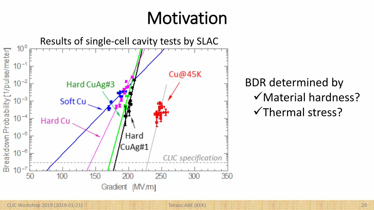
Motivation
CLIC Workshop 2019 (2019-01-21)
Results of single-cell cavity tests by SLAC
BDR determined byMaterial hardness?Thermal stress?
Tetsuo ABE (KEK) 30
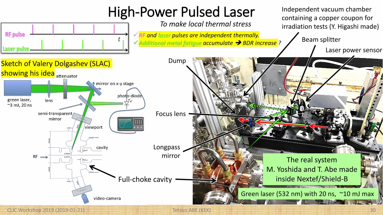
High-Power Pulsed Laser
CLIC Workshop 2019 (2019-01-21)
Sketch of Valery Dolgashev (SLAC) showing his idea
RF and laser pulses are independent thermally.Additional metal fatigue accumulate BDR increase ?
Full-choke cavity
Laser power sensor
The real systemM. Yoshida and T. Abe made
inside Nextef/Shield-B
Green laser (532 nm) with 20 ns, ~10 mJ max
Dump
Independent vacuum chamber containing a copper coupon for irradiation tests (Y. Higashi made)
Longpassmirror
Beam splitter
Focus lens
To make local thermal stress
Tetsuo ABE (KEK) 31
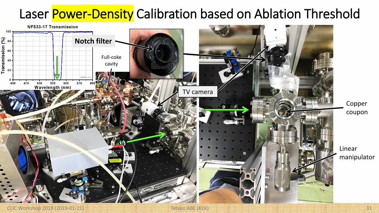
Laser Power-Density Calibration based on Ablation Threshold
CLIC Workshop 2019 (2019-01-21)
Notch filter
Linear manipulator
TV camera
Copper coupon
Full-coke cavity
Tetsuo ABE (KEK) 32
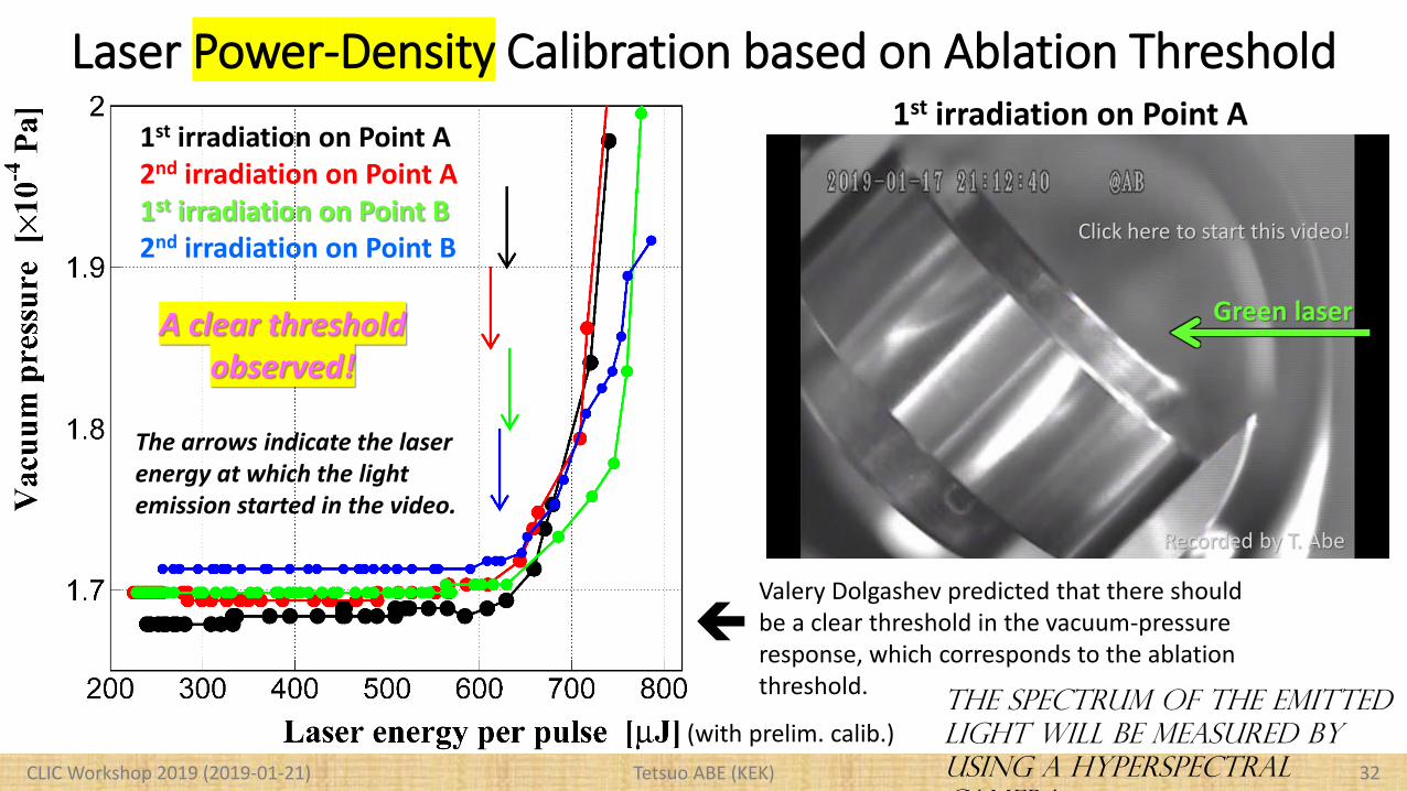
Laser Power-Density Calibration based on Ablation Threshold
CLIC Workshop 2019 (2019-01-21)
1st irradiation on Point A2nd irradiation on Point A1st irradiation on Point B2nd irradiation on Point B
1st irradiation on Point A
The arrows indicate the laser energy at which the light emission started in the video.
Valery Dolgashev predicted that there should be a clear threshold in the vacuum-pressure response, which corresponds to the ablation threshold.
The spectrum of the emitted
light will be measured by
using a hyperspectral
camera.
A clear thresholdobserved!
(with prelim. calib.)
Click here to start this video!
Recorded by T. Abe
Green laser
Tetsuo ABE (KEK) 33CLIC Workshop 2019 (2019-01-21)
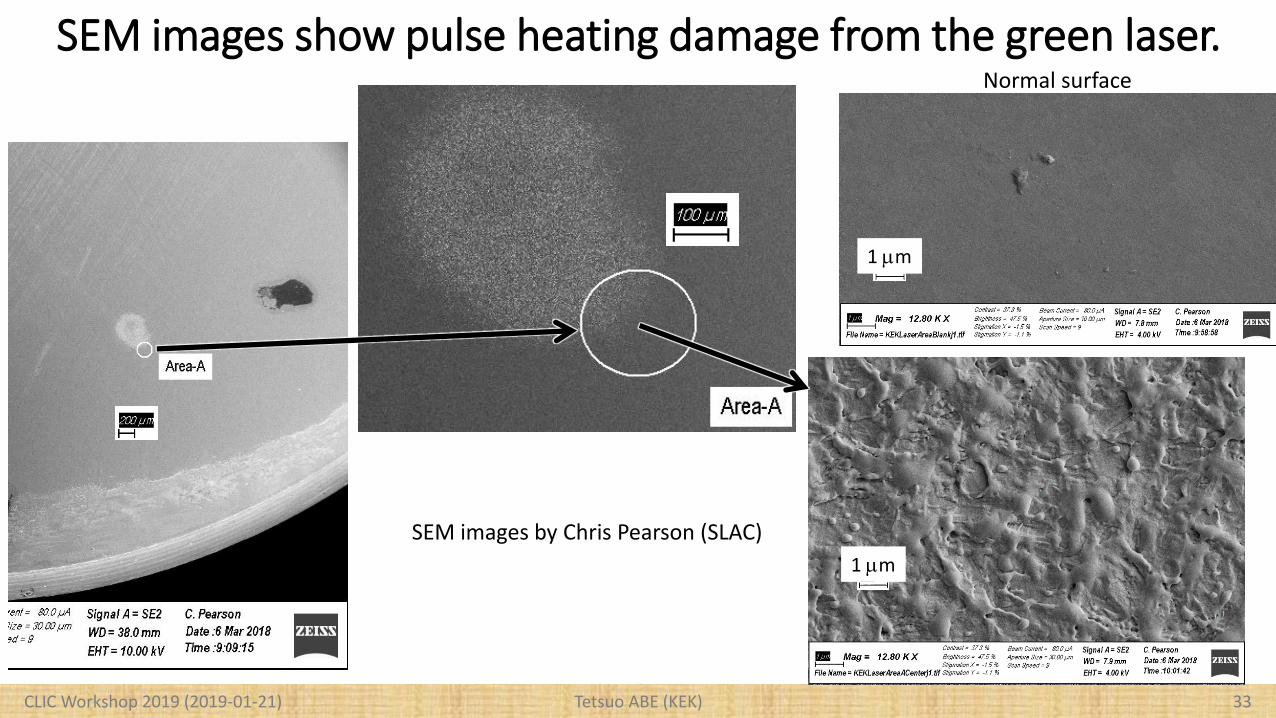
SEM images by Chris Pearson (SLAC)
1 mm
SEM images show pulse heating damage from the green laser.Normal surface
1 mm
Tetsuo ABE (KEK)
Summary TD24_QUAD status The fabrication had been successful until the EBW. Two of the four quadrants turned out not to be pure copper after the first high-temperature
process of brazing. Most probably CuZr
We have decided to started over; need additional several months. High-gradient test to be started before summer 2019
Full-choke single-cell cavity test with laser Everything just ready for high-gradient test, including the high-power pulsed laser system Compare BDRs with or without the laser irradiation for various irradiation positions
Other single-cell test cavities Two TD24-based damped cavities (with the disks brazed or diffusion-bonded) waiting to be tested Undamped cavities made of large-grain copper
34CLIC Workshop 2019 (2019-01-21)
(EBW: Electron-Beam Welding)
Tetsuo ABE (KEK) 35CLIC Workshop 2019 (2019-01-21)
Thank you for your
attention!
Tetsuo ABE (KEK) 36CLIC Workshop 2019 (2019-01-21)
Backup Slides
Tetsuo ABE (KEK) 37
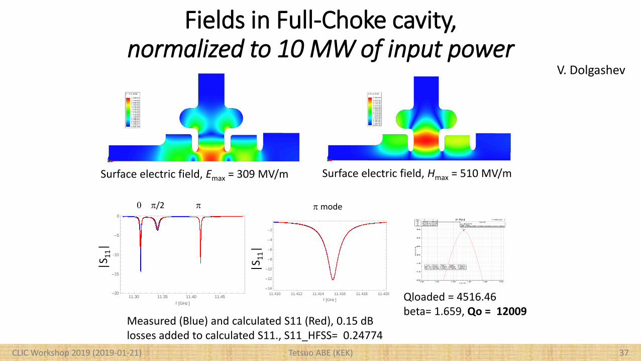
Fields in Full-Choke cavity,normalized to 10 MW of input power
CLIC Workshop 2019 (2019-01-21)
Surface electric field, Emax = 309 MV/m Surface electric field, Hmax = 510 MV/m
11.30 11.35 11.40 11.4520
15
10
5
0
f GHz
S2
2
11.410 11.412 11.414 11.416 11.418 11.420
14
12
10
8
6
4
2
f GHz
S2
2
Measured (Blue) and calculated S11 (Red), 0.15 dB losses added to calculated S11., S11_HFSS= 0.24774
Qloaded = 4516.46beta= 1.659, Qo = 12009
|S1
1|
|S1
1|
0 p/2 p p mode
V. Dolgashev
Tetsuo ABE (KEK) 38
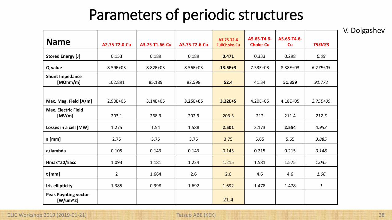
Parameters of periodic structures
CLIC Workshop 2019 (2019-01-21)
Name A2.75-T2.0-Cu A3.75-T1.66-Cu A3.75-T2.6-CuA3.75-T2.6
FullChoke-Cu
A5.65-T4.6-Choke-Cu
A5.65-T4.6-Cu T53VG3
Stored Energy [J] 0.153 0.189 0.189 0.471 0.333 0.298 0.09
Q-value 8.59E+03 8.82E+03 8.56E+03 13.5E+3 7.53E+03 8.38E+03 6.77E+03
Shunt Impedance [MOhm/m] 102.891 85.189 82.598 52.4 41.34 51.359 91.772
Max. Mag. Field [A/m] 2.90E+05 3.14E+05 3.25E+05 3.22E+5 4.20E+05 4.18E+05 2.75E+05
Max. Electric Field [MV/m] 203.1 268.3 202.9 203.3 212 211.4 217.5
Losses in a cell [MW] 1.275 1.54 1.588 2.501 3.173 2.554 0.953
a [mm] 2.75 3.75 3.75 3.75 5.65 5.65 3.885
a/lambda 0.105 0.143 0.143 0.143 0.215 0.215 0.148
Hmax*Z0/Eacc 1.093 1.181 1.224 1.215 1.581 1.575 1.035
t [mm] 2 1.664 2.6 2.6 4.6 4.6 1.66
Iris ellipticity 1.385 0.998 1.692 1.692 1.478 1.478 1
Peak Poynting vector [W/um^2] 21.4
V. Dolgashev
Tetsuo ABE (KEK) 39CLIC Workshop 2019 (2019-01-21)
End of This File