The PPS tracking system - CERN Indico
27
The PPS tracking system Performance in LHC-Run2 Prospects for LHC-Run3 M.M. Obertino Università di Torino, INFN Torino on behalf of the CMS and TOTEM collaborations
-
Upload
khangminh22 -
Category
Documents
-
view
0 -
download
0
Transcript of The PPS tracking system - CERN Indico

The PPS tracking systemPerformance in LHC-Run2
Prospects for LHC-Run3
M.M. ObertinoUniversità di Torino, INFN Torino
on behalf of the CMS and TOTEM collaborations

M.M
.Obe
rtino
–Un
iver
sità
e IN
FN T
orin
o –
IPRD
19
PROCESSES STUDIED IN DETAIL FOR THE CT-PPS TDR [CERN-LHCC-2014-021
The main target of the PPS physics program is the study of Central Exclusive Production (CEP) processes
pp à p X p
FIRST PHYSICS RESULT, JHEP07 (2018) 153
Approved in Dec. 2014 by LHCC and CERN Research Board as common CMS-TOTEM project (CT-PPS à CMS-TOTEM Precision Proton Spectrometer )
The CT-PPS - now PPS - project
Since April 2018, CT-PPS is a standard component of CMS, with name PPS
X = high-ET jets, WW, ZZ, gg …
where both protons remain intact
CERN-LHCC-2014-021
2

M.M
.Obe
rtino
–Un
iver
sità
e IN
FN T
orin
o –
IPRD
19The Precision Proton Spectrometer
ü Tracking detectors used to measure the proton displacement with respect to the beam, which istranslated into momentum loss (x) thanks to the knowledge of the beam optics
ü LHC magnets used to bend protons
LHC Sector 45
Introduction to PPS• Near beam magnetic spectrometer at IP5 of the LHC
• Joint CMS+TOTEM project to include horizontal Roman Pots in the standard, high luminosity, CMS data taking, TDR in 2014 [CERN-LHC-2014-021]
• Started in 2016 (one year early) thanks to the availability of the legacy TOTEM silicon strips detectors
• Collected data throughout the whole LHC Run 2
A. Bellora Low-x 2019 – Recent results from PPS and PPS status and prospects – Nicosia, Cyprus 4
• Two complementary measurements• Tracking detectors measure the proton displacement with respect to the beam, which is
translated into energy-momentum loss thanks to the knowledge of the beam optics• Timing detectors measure the proton arrival time in both arms w.r.t. the reference clock
that keeps the two stations synchronized, allowing the calculation of the longitudinal position of the interaction
PPS physicscase
Experimental apparatus
Operation inLHC Run 2
Tracking efficiency
Detector alignment and
proton reconstruction
(Semi)Exclusive 𝛾𝛾 → ℓ+ℓ−2016 results
Prospects for LHC Run 3
TRACKINGSYSTEM
DETECTOR STATIONSLHC Sector 56
ü Timing detectors to disentangle pile-up
PPS has been designed for measuring the scattered protons on both sides of CMS in standard LHC running conditions
Events of interest are characterized by:§ two leading protons on opposite sides of the CMS interaction point (IP)§ possibility to constrain the event kinematics by matching the momenta of the central system (X) and
the leading protons
E. Bossini’s talk on Thursday3
~200 m
IP5

Experimental challenges• Roman Pots need to operate at few mm from the beam to maximize acceptance
• RF shielding installed to limit the impedance caused by the RP insertion
A. Bellora Low-x 2019 – Recent results from PPS and PPS status and prospects – Nicosia, Cyprus 5
RF shield
Proton beamTrackingDetectors
• Detectors must tolerate high levels of non-uniform irradiation• For ~100 fb-1 (Run 2): ~5 ∙ 1015 protons/cm2
in tracking detectors• Spatial resolution required: ~10-30 μm• Timing resolution required: ∼ 20 ps, to reject high pileup
PPS physicscase
Experimental apparatus
Operation inLHC Run 2Tracking
efficiencyDetector
alignment and proton
reconstruction(Semi)Exclusive 𝛾𝛾 → ℓ+ℓ−2016 resultsProspects for
LHC Run 3
Tracking detectors: experimental challenges§ To maximize the acceptance for low x protons detectors need :
ü to operate as close as possible to the beam without affecting LHC stable operation Roman Pots (RP)
ü to be fully efficient as close as possible to their mechanical edge
§ Detectors must tolerate high levels of non-uniform irradiationà Proton flux up to ~5 · 1015 protons/cm2 for ~100 fb-1
Dose: 1.61 Mrad/ fb-1
In 2017-18 CT-PPS RPs inserted at 12 sbeam+0.3 mm (~1.5 mm) distance from the LHC beam
RADIATION LEVELSIN THE DETECTORESTIMATED USINGTOTEM DATA ANDSIMULATION (LINT ~100 fb-1)
M.M
.Obe
rtino
–Un
iver
sità
e IN
FN T
orin
o –
IPRD
19
4

M.M
.Obe
rtino
–Un
iver
sità
e IN
FN T
orin
o –
IPRD
19PPS detector configurations in LHC-Run2
Pixel + Single and double diamonds
2015 2017 20182016Strip (+Diamond)
Data taking with CMS
Exploratoryphase
Strip + Pixel +Diamonds+UFSD
Data taking in 2016, 2017 and 2018 with different detector configurations
LINT~15 fb-139% OF DATA
RECORDED BY CMS
PPS integrated luminosity in LHC-Run 2: ~115 fb-1
Data recorded with tracking RPs inserted
LINT~40 fb-188% OF DATA
RECORDED BY CMS
LINT~60 fb-193% OF DATA
RECORDED BY CMS
Exploratory phase in 2015 and 2016; very high stability in both 2017 and 2018
5

§ 3D silicon pixel sensors read out with 4 or 6 PSI46dig ROCs (same ROC usedin layers 2-3-4 of the CMS pixel detector) depending on sensor size
M.M
.Obe
rtino
–Un
iver
sità
e IN
FN T
orin
o –
IPRD
19Tracking detector – 3D pixels
Six detector planes per station tilted by 18.4° to improve resolution
2X3 (2x2) SENSOR – 6 (4) ROCs
16 mm
24 m
m
§ Mechanics and cooling adapted from TOTEM tracking system.
§ Operation at -20 °C and in vacuum ( p < 20 mbar)
Rpixportcard
6
§ Modules wire-bonded to a flex circuit connectedto the RPix portcard (interface between modulesand front-end electronics)
§ Same front-end boards for data (FED) and control (FEC) as for the CMS Phase I pixel trackerupgrade
§ Pixel area: 100x150 µm2
§ Sensor thickness: 230 µm§ Column depth: 200 µm§ Column diameter: 10 µm§ 200 µm slim edge

2008
JIN
ST 3
S08
007
Figure4.13:TwoRPhybridsmountedback-to-back.EachhybridcarriesthesilicondetectorandfourVFATreadoutchips.
4.4On-detectorelectronics
Thegeneralisedelectronicsaredescribedinmoredetailinchapter7.Onlytheelectronicboardsthatarerelevanttothemechanicalconstructionandthedetectormonitoringarediscussedhere.Thesilicondetectorhybrid(figure4.13)carriesthedetectorwith512stripswire-bondedtotheinputchannelsof4readoutchips“VFAT”(section7.1),andaDetectorControlUnit(DCU)chip.EachVFATprovidestrackingandtriggergenerationsignalsfrom128strips.TheDCUchipisusedtomonitordetectorleakagecurrents,powersupplyvoltagesandtemperature.Viaan80pinconnectoreachVFATwillsendthetriggeroutputsandtheserialisedtrackingdatafromallstripstothemotherboard,togetherwithclockandtriggerinputsignals,HVandLVpower,andconnectionsforaheaterandaPT100resistancethermometerfortemperaturecontrol.
Duetothe±45�orientationofthedetectorstrips,flippingthedetectorhybridandmountingitfacetofacewiththenextoneresultsinmutuallyorthogonalstripsgivingtheuandvcoordinateinformation.Toavoidlosingspaceinbetweentwohybrids,allelectricalcomponentsaremountedononesidesuchthattheydonotoverlapforthetwocardsmountedfacetofaceandthattheycanbeseparatedbyonlyonecomponentheight.
Insuchway10detectorhybridscloselyarrangedin5pairs,canbeconnectedtoonemoth-erboardfeedingallelectricalconnectionsthroughtheflangebetweenthepot’ssecondaryvacuumandtheoutsideworldatatmosphericpressure.
Themotherboard(figure4.14)hostsclockandtriggerdistributioncircuitry,GigabitOpticalHybrids(GOH)—threefordataandtwofortriggerbittransfer,twoCoincidenceChipmezzanines,LVDS-to-CMOSconverters,TriggerVFATmezzanine,ControlUnitmezzanineCCUM,RadiationMonitorcircuitryandtemperaturesensors.Thebinarytrackingdataarestoredinadigitalmemory
–23–
7
M.M
.Obe
rtino
–Un
iver
sità
e IN
FN T
orin
o –
IPRD
19Tracking detector - Silicon strips
§ 512 strips per plane, ±45o orientation§ Thickness: 300 µm - Pitch: 66 µm§ Edgeless technology: ~50 µm inactive edge
(CTS on the edge facing the beam)§ Resolution ~20 µm§ Designed for low-luminosity running:⚠ Lifetime: up to 5x10¹⁴ p/cm2 integrated flux⚠ No multi-track capability
Digital readout provided by 4 VFAT2chips located on a flexible circuitconnected to a motherboard
2008 JINST 3 S08007
!"#$%&'()*+%,
-"
(.
%.!'/)#0,#)))))
!'**#%/)/#*1+%$/+%,)*+%,
-"
2+34
%&/5(#)6'"7
(.
&!
89:; 89;
<=)>1
?/*+(
6+$?+%,)#"#!/*@0#
?/*+(
8AB
?#%?+/+C#)C@"'1#
Figure 4.8: Cross-section of a silicon detector with CTS in the plane parallel to the strips and itsbiasing scheme.
0
50
100
150
200
250
300
0 50 100 150 200 250 300 350 400 450 500
+0+50+100+150+200
VPotential
20
150
100
50
5
x [um]
y [u
m]
Figure 4.9: Left: potential distribution at the edge of a 300 µm thick silicon pad detector with CTSfor a bias voltage of 200 V. The calculation extended up to 500 µm into the detector from the cutedge. Right: electric potential at the cut edge with an almost linear behaviour.
any further diffusion of this edge current into the sensitive volume, another implanted ring — theClean-up Ring (CR) — can be placed between the CTR and the sensitive volume. The CTS and itsbiasing scheme are shown in figure 4.8.
For devices with this type of CTS, the leakage current in the sensitive volume (IBE) whichcontributes to noise is not affected by the edge current (ICTR + ICR). The leakage current and theedge current have been shown to be completely decoupled. Moreover, for such devices, the chargecollection efficiency has been shown to rise steeply from the edge of the sensitive volume reachingfull efficiency within a few tens of micrometers (see section 4.6.1.1).
The electric potential distribution at the edge of a device with CTS has been modelled takinginto account the highly damaged surface at the chip cut, where the irregularities within the firstatomic layers could be assimilated to amorphous silicon. The results of this modelling have showngood consistency with the experimental results [14]. The potential distribution calculated with ISETCAD [15] is shown in figure 4.9.
– 20 –
Same detectors used in the tracking RPs of the TOTEM experiment [2]
2008 JINST 3 S08007
Figure 4.10: Picture of a Planar Edgeless Detector with CTS (top). The magnification of a portionof the chip cut region (bottom) shows the details of the CTS.
4.3.2 The silicon detector for the TOTEM Roman Pots
The advantages offered by the CTS have led TOTEM to choose this technology for the RP detec-tors. Geometry and granularity have been adapted to the specific requirements on surface coverageand spatial resolution.
The detectors have been developed and produced in a joint effort of the TOTEM group atCERN and Megaimpulse, a spin-off company from the Ioffe Physico-Technical Institute in St.Petersburg (Russia). These devices are single-sided AC p+-n microstrip detectors with 512 stripsand a pitch of 66 µm processed on very high resistivity n-type silicon wafers (> 10kWcm), 300 µmthick. All of them have the CTS as described in section 4.3 on one edge, i.e. the edge facingthe beam. At one end of the strips an integrated pitch adapter reduces the inter-strip distancefrom 66 µm to 44 µm, producing four separated groups of 128 channels. This allows direct wirebonding to the readout chip VFAT. A picture of the planar edgeless Silicon detector for the TOTEMRoman Pots and a detail of the CTS are shown in figure 4.10. In these sensors the biasing is madevia “punch-through” from a biasing electrode placed inside the CR. On all the sides where thesensitivity at the edge is not required, the CTS is integrated into a standard voltage terminatingstructure. The strips on the detector are at an angle of 45� with respect to the edge facing thebeam.
4.3.3 Electrical characterisation
For the detector polarised according to the biasing scheme shown above, the typical values ofcurrents measured at the CTR and the CR, ICTR + ICR, are compared to the current measured at thebiasing electrode, IBE, and shown in figures 4.11 and 4.12. There is a difference of four orders ofmagnitude between the current at the biasing electrode flowing through the sensitive volume of thedetector and the one flowing through CR and CTR. This evidences that virtually all the leakage
– 21 –
35 m
m
VFAT2
[2] The Totem Collaboraytion et al., The TOTEM Experiment at the CERN Large Hadron Collider, 2008 JINST 3 S08007
10 planes of micro-strip silicon detectors per RP
Front-end boards for data and control, mechanics and cooling from TOTEM tracking system.
CURRENT TERMINATING STRUCTURE (CTS)

DETECTOR PERFORMANCE
2018 DETECTOR CONFIGURATION
2017 DETECTOR CONFIGURATION
M.M
.Obe
rtino
–Un
iver
sità
e IN
FN T
orin
o –
IPRD
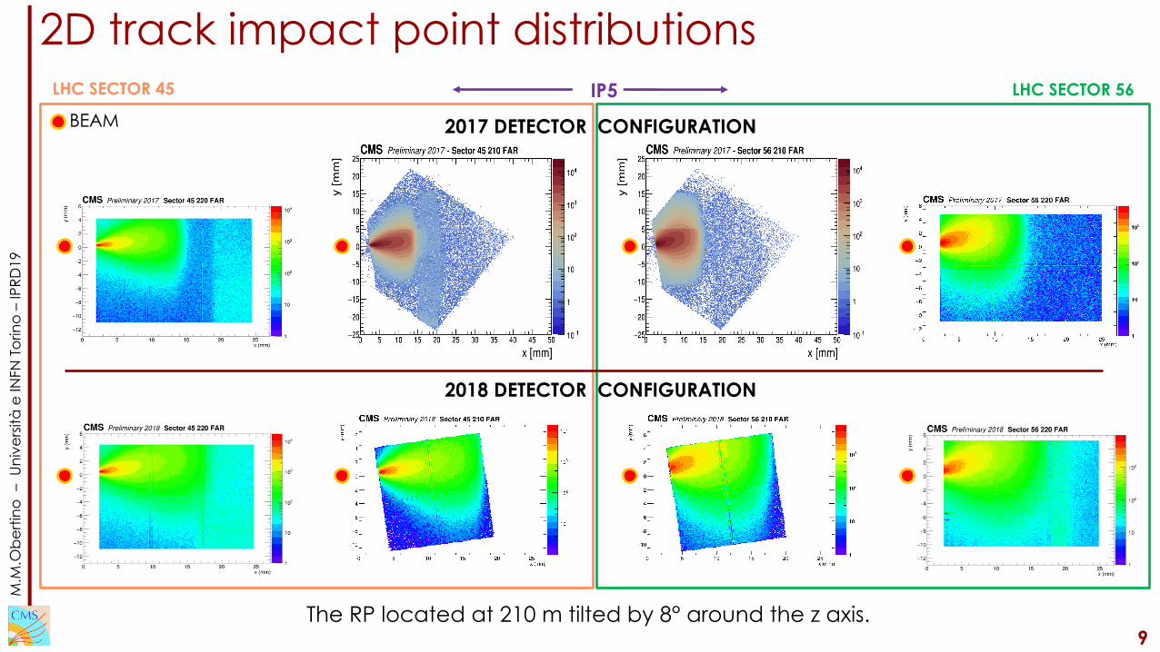
192D track impact point distributions
LHC SECTOR 56LHC SECTOR 45 IP5BEAM
9The RP located at 210 m tilted by 8° around the z axis.

M.M
.Obe
rtino
–Un
iver
sità
e IN
FN T
orin
o –
IPRD
19Si-strip detector efficiency Two major sources of inefficiency (radiation damange and no multi-track capability) studied separately
~50% efficiency at pile-up 40
Only single-track events can be reconstructed with the Si-strip detector
à efficiency decreases with number ofinteractions per bunch crossing (pile-up)
Pile-up10 20 30 40 50 60
0.9
0.8
0.7
0.6
0.5
0.4
0.3
Effic
ienc
y 7
6
5
4
3
2
1
0
2017 postTS2CMS Preliminary
Pile-up
NUMBER OF TRACKS RECONSTRUCTED BY THE PIXEL DETECTOR AS A FUNCTION OF PILE-UP
More than 40% of events with multiple tracks in standarddata taking conditions (PU~40)
The increasing number of multi-track events with pile-upshows the advantage of a pixel detector with respect to astrip one
10

M.M
.Obe
rtino
–Un
iver
sità
e IN
FN T
orin
o –
IPRD
19Effect of radiation on strip detector efficiency
Radiation damaged area clearly visible, especially in sector 45
Efficiency maps produced:§ for the region relevant for physics (covered by the pixel detector acceptance, and below the
collimator aperture limits)§ with the first data collected (LLINT ~ 2.4 fb-1)
à Detector packages replaced during 2017 LHC technical stop11

M.M
.Obe
rtino
–Un
iver
sità
e IN
FN T
orin
o –
IPRD
19Pixel performance: efficiency
RP EFFICIENCY AT BEGINNING OF DATA TAKING
LINT = 8 fb-1 LINT = 11.7 fb-1
Overall very good performance - average efficiency above 99%
The lower efficiency region visible in the right part of the two maps is due to the fact that both RPshave one plane 2x2 not covering that region, and to the presence of malfunctioning ROCs on other planes.
Efficiency estimation based on tracks reconstructed within the same tracking station
SIMILAR RESULTS IN 2018
Less than 0.05% bad/noisy pixels12

M.M
.Obe
rtino
–Un
iver
sità
e IN
FN T
orin
o –
IPRD
19Radiation effect on the ROCPixel ROC (PSI46dig) not optimised for non-uniform irradiation.
Non-uniform irradiation causes a difference between the analog current supplied to the most and the least irradiated pixels.
PIXELS NOT RESPONDING IN THE SAME 25 ns CLOCK WINDOW (BX)
ü Irradiation studies performed before installation at LHC showed that after a dose corresponding to LINT (LHC) ~8 fb-1, the drift of the useful time window for signals in most irradiated pixels exceeds 25 ns
ü To mitigate the impact on the data quality, the tracking stations were lifted up during LHC technicalstops (TS) to shift the occupancy maximum away from the damaged region.
Time
Volta
ge NON-IRRADIATED PIXELHIGHLY IRRADIATED PIXEL
13

M.M
.Obe
rtino
–Un
iver
sità
e IN
FN T
orin
o –
IPRD
19
BEGINNING OF DATA TAKING 21.0 fb-1 50.3 fb-1 57.8 fb-1
SECTOR45
SECTOR56
TS TS
Effect of radiation on RP efficiency (2018)
RP SHIFTED BY 0.5 mm DOWNWARDS
RP SHIFTED BY 0.5 mm DOWNWARDS
EVOLUTION OF THE RP EFFICIENCY MAP IN THE DETECTOR REGION CLOSEST TO THE BEAM FOR RP 220 FAR (worst case)
14
Deterioration of the RPefficiency caused bythe radiation damage[ always in x=0, y=0 ]
BEAM

M.M
.Obe
rtino
–Un
iver
sità
e IN
FN T
orin
o –
IPRD
19
IRRADIATION PEAK AREA
Average efficiency calculated every ∼ 1 fb-1 in the critical region around the irradiation peak
Drop in the efficiency due to irradiation clearly visible in the critical region; recovery after eachLHC technical stop (TS) due to vertical movement of the RPs.
à This plot will be used as monitoring tool in LHC-Run3
IRRADIATION PEAK AREA
Effect of radiation on RP efficiency (2018)
15

M.M
.Obe
rtino
–Un
iver
sità
e IN
FN T
orin
o –
IPRD
19
PPS prospects for LHC-Run3PPS will operate as a full CMS subsystem in LHC-Run3 (2021 - 2023)
TRACKER SYSTEM in LHC-Run3§ 2 Roman Pots per side, at 210 m and 220 m from CMS-IP; 6 detector planes
per RP (same as 2018)
§ New 3D silicon pixel sensors will be produced by FBK
ü single side technologyü 2x2 sensor geometryü 150 µm thickü 2E electrode configuration
§ ROC: PROC600 (same as layer 1 of the CMS pixel detector)
§ New flex circuit design (different ‘look’ but very similar design)
§ New detector package with internal movement system, to better distributethe radiation damage
à 12 positions spaced by 500 µm, possibility of handlingmore than 50 fb-1 with minimal efficiency loss
PPS General Meeting, CERN23/09/2019
Sensor production for Run3Production on 6′′ wafers; 3D sensors with one-side columns, ’2E’ geometry• “2×2” and “1×1” sensor sizeContract through CERN tender:• minimal requirement of 100 good 2×2 sensors;• minimal requirement of 4 good (≥50% yield) wafers;Contract adjudged to FBK Trento• delivery in February-March 2020
!2
Wafer layout
Cell detail
PPS prospects for Run 3
• PPS approved for operation as standard CMS subsystemin LHC Run 3 (2021-2023)
• Experimental apparatus:• Tracking:
• 2 horizontal stations with silicon 3D pixels sensors
(similar to the 3D pixels designed for the
CMS Phase2 Tracker R&D)
• PROC600 readout chip
(same as CMS pixel detector layer 1)
• New internally motorized detector package,
to distribute the radiation damage
and reduce its impact
• Timing:
• 2 horizontal stations
equipped with double-layer diamond sensors
• Optimized readout electronics
A. Bellora Low-x 2019 – Recent results from PPS and PPS status and prospects – Nicosia, Cyprus18
PPS physics
case
Experimental
apparatus
Operation in
LHC Run 2
Tracking
efficiency
Detector
alignment and
proton
reconstruction
(Semi)Exclusive
𝛾𝛾 → ℓ+ℓ−2016 results
PPS
Prospects
PPS General Meeting, CERN23/09/2019
New support structureFirst prototype with new design produced in INFN Ge workshopFeatures:• simplified, easier-to-assemble structure;• reduced friction, with rolling balls;• ad-hoc mechanical coupling with piezo-actuator
for bi-directional active movements;• simple (⟹ rad-hard) position sensor includedTested in Genova starting end of July• successful movement tests in both directions,
under realistic work conditions;• assembly procedure critical: steps to be followed
with care;• few improvements implemented; others planned
!4
DESIGN AND FIRST PROTITYPE OFTHE NEW DETECTOR PACKAGE
PIEZOELECTRICMOTOR
NEW FLEXCIRCUIT
16

Conclusion
Tracking system has been successfully operated since the beginningof LHC-Run2 with overall very good performance:
§ smooth data taking§ high efficiency and tracking capability
despite the high and non uniform irradiation conditions
The preparation for LHC-Run 3 is ongoing• New detectors are getting ready to be installed for the future
data taking• A rich physics programme lies ahead, with many final states to be
studied
M.M
.Obe
rtino
–Un
iver
sità
e IN
FN T
orin
o –
IPRD
19
17
PPS has proven the feasibility of continuously operating a near-beam proton spectrometer at a high-luminosity hadron collider and has collected ~!!" fb-1 of data during LHC-Run 2

BACKUP SLIDES

M.M
.Obe
rtino
–Un
iver
sità
e IN
FN T
orin
o –
IPRD
19
Data takingCT-PPS collected:§ ~ 88% of the full statistics recorded by CMS in 2017
à ~ 40 fb-1 with RP data§ ~ 93 % of the full statistics recorded by CMS in 2018
à ~ 60 fb-1 with RP data
CMS Online Luminosity
CMS Online Luminosity
MD+TS1+high b run
MD
MD+TS2
CMS Online Luminosity
19

Tracking Detector - Silicon 3D Pixels
3D sensors produced by CNM: double side process with no passing-through columns
§Pixel area: 100x150 µm2
§ Sensor thickness: 230 µm§Column depth: 200 µm§Column diameter: 10 µm
ü 200 µm slim edge made of a triple p-type column fence; reduced at ~50 µm by increasing the bias voltage (for 2E electrode configuration)
2E and 1E electrode configuration
100
µm
200 µm
3D sensors bump-bonded to the PSI46dig ROC extensively testedin laboratory and with beam at FNAL [1]
ü Spatial resolution for 2E (1E) sensors tilted by 20° : 22 µm (25 µm)
M.M
.Obe
rtino
–Un
iver
sità
e IN
FN T
orin
o –
IPRD
19
3D sensor technology chosen for its intrinsic high radiation hardness and the possibility to implementslim edges.
[1] F. Ravera, The CT-PPS tracking system with 3D pixel detectors, Pixel2016 Workshop
VBIAS=40V
20
M.M
.Obe
rtino
–Un
iver
sità
e IN
FN T
orin
o –
IPRD
19
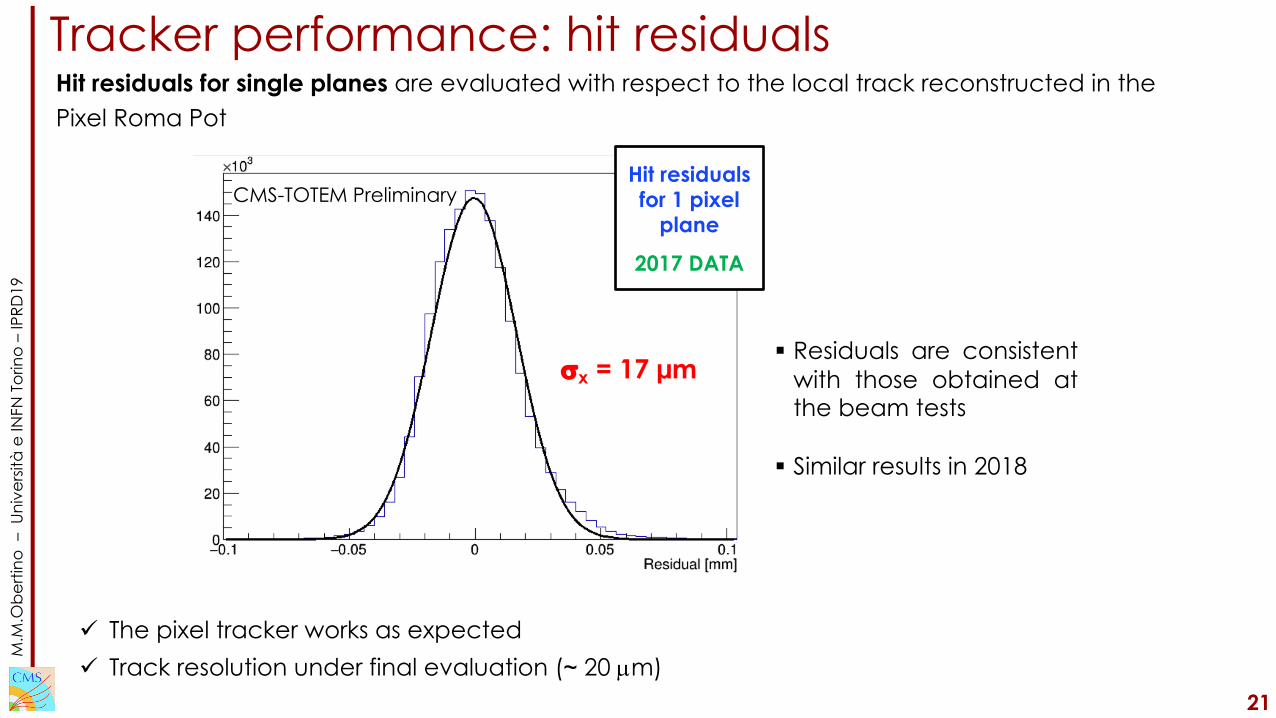
sx = 17 µm
Hit residuals for 1 pixel
plane
2017 DATA
Tracker performance: hit residuals
CMS-TOTEM Preliminary
§ Residuals are consistentwith those obtained atthe beam tests
§ Similar results in 2018
ü The pixel tracker works as expected ü Track resolution under final evaluation (~ 20 µm)
Hit residuals for single planes are evaluated with respect to the local track reconstructed in the Pixel Roma Pot
21

M.M
.Obe
rtino
–Un
iver
sità
e IN
FN T
orin
o –
IPRD
19
The deterioration of theRP efficiency caused bythe radiation damage
8.8 fb-1 18.9 fb-1 29.5 fb-1TS
Effect of radiation on RP efficiency (2017)EVOLUTION OF THE RP EFFICIENCY MAP IN THE DETECTOR REGION CLOSEST TO THE BEAM FOR LHC SECTOR 45
Detectors in sector 56 suffered smaller radiation damage (barely visible in the maps) because ofthe different irradiation profile.
RP SHIFTED BY 1 mm UPWARDS As the integrated luminosity
increases, a second damageregion appears at the newoccupancy maximum
BEAM[ always in
x=0, y=0 ]
22

23
M.M
.Obe
rtino
–Un
iver
sità
e IN
FN T
orin
o –
IPRD
19
COMPLEMENTARY AREA
IRRADIATION PEAK AREAAverage efficiency calculated every ∼ 1 fb-1 :§ in the critical region around the irradiation peak (left plot)§ in the complementary region (right plot)
Drop in the efficiency due to irradiation clearly visible in thecritical region; recovery after each LHC technical stop (TS)due to vertical movement of the RPs.Average efficiency in the complementary area high andalmost constant during the whole data taking.
à These plots will be used as monitoring tool in LHC-Run3
IRRADIATION PEAK AREA COMPLEMENTARY AREA
Effect of radiation on RP efficiency (2018)
23

M.M
.Obe
rtino
–Un
iver
sità
e IN
FN T
orin
o –
IPRD
19RP efficiency versus proton fractional momentum loss (x)
Track efficiency versus the proton fractional momentum loss x at the beginning and at the endof 2018 data taking period for sector 45 (left) and sector 56 (right).§ Efficency shown in the x range corresponding to the detector acceptance§ Efficiency in each x bin evaluated using the values from the RP efficiency maps
These plots show the impact of the sensor radiation damage on physics studies24

M.M
.Obe
rtino
–Un
iver
sità
e IN
FN T
orin
o –
IPRD
19
◦ RPs consist of 5+5 planes with mutually perpendicular strip orientations (denoted U and V)
◦ If two tracks pass through the detector (black dots), they activate 2 U strips (blue) and 2 Vstrips (red), yielding 4 crossings out of which only 2 are real
Only single-track events can be reconstructed
Si strip detectors – “multi-track” inefficiency
Efficiency evaluated, using zero-bias data, as:
Sufficient signal = one or more track patterns recognised OR hit multiplicity greaterthan threshold for pattern-recognition to give up
25

M.M
.Obe
rtino
–Un
iver
sità
e IN
FN T
orin
o –
IPRD
19Effect of radiation on strip detector efficiency
Radiation damaged area clearly visible, especially in sector 45
Efficiencies vs ξ measured in the most irradiated region of y (plotted for ξ values below aperture limitations)
26

M.M
.Obe
rtino
–Un
iver
sità
e IN
FN T
orin
o –
IPRD
19
Roman Pots
Each station includes 3 RPs
Tracking RPs equipped with a thinwindow 150 µm thick toward the
beam
Cylindrical RP specifically designedfor PPS to reduce the impedance andhost larger detectors.
Equipped with a 300 µm thick windowtowards the beam (thickness requiredto compensate the pressure gradienton the larger window).
No vertical stations, alignment doneby propagating tracks from the tracking stations.
27