ELECTRICAL ACTIVATION STUDIES OF SILICON IMPLANTED
311
ELECTRICAL ACTIVATION STUDIES OF SILICON IMPLANTED ALUMINUM GALLIUM NITRIDE WITH HIGH ALUMINUM MOLE FRACTION DISSERTATION Elizabeth A. Moore AFIT/DS/ENP/08-D01 DEPARTMENT OF THE AIR FORCE AIR UNIVERSITY AIR FORCE INSTITUTE OF TECHNOLOGY Wright-Patterson Air Force Base, Ohio APPROVED FOR PUBLIC RELEASE; DISTRIBUTION UNLIMITED.
-
Upload
khangminh22 -
Category
Documents
-
view
0 -
download
0
Transcript of ELECTRICAL ACTIVATION STUDIES OF SILICON IMPLANTED
ELECTRICAL ACTIVATION STUDIES OF SILICON IMPLANTED
ALUMINUM GALLIUM NITRIDE WITH HIGH ALUMINUM MOLE
FRACTION
DISSERTATION
Elizabeth A. Moore
AFIT/DS/ENP/08-D01
DEPARTMENT OF THE AIR FORCEAIR UNIVERSITY
AIR FORCE INSTITUTE OF TECHNOLOGY
Wright-Patterson Air Force Base, Ohio
APPROVED FOR PUBLIC RELEASE; DISTRIBUTION UNLIMITED.

The views expressed in this dissertation are those of the author and do not reflect the official policy or position of the United States Air Force, Department of Defense, or the United States Government.

AFIT/DS/ENP/08-D01
ELECTRICAL ACTIVATION STUDIES OF SILICON IMPLANTED ALUMINUM GALLIUM NITRIDE WITH HIGH ALUMINUM
MOLE FRACTION
DISSERTATION
Presented to the Faculty
Graduate School of Engineering and Management
Air Force Institute of Technology
Air University
Air Education and Training Command
In Partial Fulfillment of the Requirements for the
Degree of Doctor of Philosophy
Elizabeth A. Moore, BS, MS
December 2007
APPROVED FOR PUBLIC RELEASE; DISTRIBUTION UNLIMITED

AFIT/DS/ENP/08-D01
Abstract
This research demonstrates a method for producing highly conductive Si-
implanted n-type aluminum gallium nitride (AlxGa1-xN) alloys, and represents a
comprehensive analysis of the resulting material's electrical and optical properties as a
function of Al mole fraction, anneal temperature, anneal time, and implantation dose.
Highly conductive alloys are critical to the fabrication of devices operating in deep UV,
high-temperature, high-power, and high-frequency environments, and thus this research
is significant in regard to the application of such devices. The AlxGa1-xN wafers of this
study, with Al concentrations of 10 to 50%, were implanted at room temperature with
silicon ions at energies of 200 keV with doses of 1x10¹⁴, 5x10¹⁴, and 1x1015 cm-2 and
annealed from 1100 to 1350 ºC for 20 to 40 minutes in flowing nitrogen. Excellent
activation was achieved for each of the implanted silicon doses for all of the five Al mole
fractions studied, with most activation efficiencies above 90%. These activation
efficiencies are the highest reported activations, to the best of my knowledge. The
Al0.1Ga0.9N annealed for 40 minutes at 1200 ºC had electrical activations of 73, 94, and
100% for implanted silicon doses of 1x10¹⁴, 5x10¹⁴, and 1x1015 cm-2, respectively.
Higher activations of 83, 100, and 100% were achieved for the Al0.2Ga0.8N implanted
with the same doses and annealed at 1300 ºC for 20 minutes. These same annealing
conditions, of 1300 ºC for 20 minutes, produced slightly lower activations of 74, 88, and
iv
v
100% for the Si-implanted Al0.3Ga0.7N. Exceptional activation efficiencies were obtained
for each of the implanted silicon doses in the Al0.4Ga0.6N. The Al0.4Ga0.6N implanted
with a dose of 1x1014 cm-2 silicon ions had an activation of 99% following a 20 minute
anneal at 1350 ºC, while the samples implanted with the higher silicon doses of 5x10¹⁴
and 1x1015 cm-2 had activations of 100 and 96%, respectively, after being annealed at
1200 ºC for 40 minutes. The Al0.5Ga0.5N exhibited activation efficiencies of 100, 96, and
66% for the three implanted silicon doses after being annealed at 1300 ºC for 20 minutes.
The mobilities were found to decrease as the Al concentration of the AlxGa1-xN was
increased from 10 to 50% and also as the implanted silicon dose was increased. Typical
mobilities ranged from 101 cm2/V·s for the Al0.1Ga0.9N implanted with 1x1014 cm-2
silicon ions to 35 cm2/V·s obtained for the Al0.5Ga0.5N implanted with 1x1015 cm-2 silicon
ions. The cathodoluminescence results support the electrical results in determining the
optimal annealing conditions.

Acknowledgements
Writing this dissertation has been one of the most significant academic challenges
I have ever had to face. Without the support, guidance and patience of my colleagues,
family and friends I would never have been able to complete this document. To all these
people I owe my deepest gratitude. I must first thank my husband for his unwavering
support and encouragement through all the years of graduate school, for without him this
effort would be worth nothing. His love, patience, and support gave me the foundation I
needed to complete this study. I am eternally grateful to my family for raising me in an
environment that encouraged and cultivated my inquisitive mind. Their support was also
instrumental in the development and completion of this project. I would like to thank my
advisor, Dr. Yeo, for his guidance, support and sense of humor throughout this endeavor.
He has been wonderful to work with and has taught me a lot, not only about physics, but
also about developing from a student to a professional. I would like to acknowledge my
committee members for their time and expertise. I would like to thank the AFIT lab
technicians, especially Mike Ranft and Greg Smith, for all of their efforts in keeping my
lab equipment functioning and me safe. They have been an invaluable resource for
experimental design questions and maintenance. I would also like to thank the
AFIT/ENP staff, in particular Jo Pollard, Kevin Pope and Jennifer Meier, for all their
efforts and directions. Finally, I would like to thank the many friends I have made along
the way, Matt Lange, Catherine Taylor, Glen Kading, and Greg Pitz for helping me to
remember that life is a journey not a destination, and for reminding me to laugh and have
fun along the way.
vi

Table of Contents
Page
Abstract .................................................................................................................. iv
Acknowledgements................................................................................................ vi
Table of Contents.................................................................................................. vii
List of figures......................................................................................................... ix
List of Tables ........................................................................................................ xx
I. Introduction ...................................................................................................... 1 The Electronic Revolution ................................................................................ 2 The Era Beyond Silicon.................................................................................. 11 A New Material, AlxGa1-xN ............................................................................ 14 Methodology................................................................................................... 18
II. Theory ............................................................................................................. 20 Crystal Structure of Solids .............................................................................. 21 Crystal Growth................................................................................................ 23 Band Structure ................................................................................................ 26 Semiconductor Physics ................................................................................... 33 Effects of Impurities ....................................................................................... 36
III. Characterization Techniques........................................................................... 43 Electrical Properties ........................................................................................ 43
Hall Effect Theory ........................................................................................ 44 Hall Effect Measurements............................................................................. 48
Optical Properties............................................................................................ 50 Optical Theory .............................................................................................. 50 Cathodoluminescence ................................................................................... 54 Cathodoluminescence Measurements........................................................... 54
IV. Experimental Method ..................................................................................... 57 Sample Specifications..................................................................................... 57 Cathodoluminescence Measurements............................................................. 59 Sample Cutting................................................................................................ 62 Ion Implantation.............................................................................................. 64 Annealing........................................................................................................ 69
vii

viii
Page
AlN Encapsulant Removal.................................................................................... 79 Ohmic Contacts............................................................................................... 79
V. Results.............................................................................................................. 82 Silicon Implanted Al0.1Ga0.9N.......................................................................... 87
Room Temperature Hall Effect Measurements ............................................ 88 Temperature-Dependent Hall Effect Measurements .................................. 104 Low Temperature Cathodoluminescence Measurements ........................... 114
Silicon Implanted Al0.2Ga0.8N........................................................................ 129 Room Temperature Hall Effect Measurements .......................................... 130 Temperature-Dependent Hall Effect Measurements .................................. 142 Low Temperature Cathodoluminescence Measurements ........................... 148
Silicon Implanted Al0.3Ga0.7N........................................................................ 158 Room Temperature Hall Effect Measurements .......................................... 159 Temperature-Dependent Hall Effect Measurements .................................. 173 Low Temperature Cathodoluminescence Measurements ........................... 180
Silicon Implanted Al0.4Ga0.6N........................................................................ 191 Room Temperature Hall Effect Measurements .......................................... 192 Temperature-Dependent Hall Effect Measurements .................................. 207 Low Temperature Cathodoluminescence Measurements ........................... 214
Silicon Implanted Al0.5Ga0.5N........................................................................ 224 Room Temperature Hall Effect Measurements .......................................... 225 Temperature-Dependent Hall Effect Measurements .................................. 240
Summary ........................................................................................................ 256
VI. Conclusions................................................................................................... 258 Recommendations for Future Research ....................................................... 265
Appendix A......................................................................................................... 266 Hall Effect Measurements............................................................................. 266 Cathodoluminescence Measurements........................................................... 269
Appendix B ......................................................................................................... 271 Silicon Dose: 1x1014 cm-2 ............................................................................. 272 Silicon Dose: 5x1014 cm-2 ............................................................................. 275 Silicon Dose: 1x1015 cm-2 ............................................................................. 278
References.......................................................................................................... 281
List of figures
Figure Page
2.1 The crystal structure of ZnS is shown in both the (a) zincblende and (b) wurtzite structures. The zincblende structure has cubic symmetry and thus has only one lattice constant while the wurtzite formation has two lattice constants due to its hexagonal symmetry…………………………………………………………………………...23
2.2 An energy band diagram for AlN which illustrates a variety of points of symmetry within the first Brillioun zone. The conduction band minimum and the valance band maximum both occur at the Γ point in k-space………………………………………..…………………………….……30
2.3 The first Brillioun zone of the hexagonal crystal structure of AlN showing various points of symmetry of the crystal structure……………………………………………………………………….……32
2.4 Impurity donor and acceptor levels in eV for various atoms in GaAs (22)……... …………………………………………………………40
3.4 A schematic diagram illustrating the direction of the Lorentz Force, induced electric field, applied magnetic field and applied current to demonstrate the van der Pauw Hall Effect………………..……………..45
3.2 A schematic diagram of the Lake Shore 7505 automated Hall measurement system for carrier concentration, resistivity, and temperature-dependent measurements. The board for room temperature measurements is illustrated and the system is also equipped with a low temperature and high temperature operating head……………………..……...49
3.3 A two dimensional illustration of the most common radiative transitions that take place in semiconductors. The transitions shown are: the band-to-band transition (a), the free exciton transition (b), the neutral donor free hole recombination (c), a free electron transitioning to a neutral shallow acceptor (d), and the donor acceptor transitions for shallow and deep states (e) and (f) respectively…………………………………………………………………………52
ix

Page
3.1 Schematic Diagram of the cathodoluminescence experimental setup designed to excite the samples through electron bombardment. It has both temperature and energy dependent capabilities…………………...……56
4.1 CL Spectra taken at 7.4 K on the original wafers sent from SET, Inc. in order to investigate the quality of the material, as well as determine the Al mole fraction of each wafer………………………………..………………..60
4.2 The transmission spectrum sent from SET, Inc., for the Al0.5Ga0.5N wafer that shows a clear transition at 271nm indicating a good quality wafer that has 51% Al concentration………………………………...……………..62
4.3 A diagram to illustrate how the wafers are divided in preparation (a) for ion implantation and (b) for the annealing processes. The wafer shown in (a) is marked with the Si implantation dose for each quadrant. The wafer quadrant in (b) illustrates the naming system to track the location of the samples……………………………....………….………..64
4.4 A schematic diagram of a typical ion implantation experimental design………………………………………………………………………….…....65
4.5 The predicted TRIM depth profiles for Si ions at various energies and Au at 300 keV in to GaN with a 500 Å AlN encapsulant to illustrate the effects that the ion’s energy and mass have on the shape of the depth profile………………………...……………………………...………..68
4.6 An illustration of the lattice disorder that results from the ion implantation of a light and heavy ion, respectively………………………...………71
4.7 The temperature profile for the Oxy-Gon furnace used for the high temperature post implantation anneal. It takes about 75 seconds for the heat zones temperature to stabilize after the samples are introduced into the chamber and also to bring the samples up to temperature……………………..77
4.1 4.8 The etch rate of AlN on AlxGa1-xN as a function of Al mole fraction when placed in a 5 M solution of KOH and DI water. The etch rate decreases rapidly as the Al concentration of the material increases…………...…..80
x

Page
5.1 Silicon ion implantation profiles generated from TRIM code to illustrate the loss of ions from the removal of the 500 Å AlN encapsulant. The room temperature implantation conditions were silicon ions with an energy of 200 keV in a dose of 1x1015 cm-2 which produce peak concentrations of 5.62x1019 cm-3 and 5.78x1019 cm-3 for Al0.1Ga0.9N and Al0.5Ga0.5N, respectively. The AlxGa1-xN surface is at x = 0 on the graph………………...………………….………………………..84
5.2 Room temperature sheet carrier concentrations for Al0.1Ga0.9N implanted with Si at 200 keV at room temperature with doses of 1x10¹⁴, 5x10¹⁴, and 1x1015 cm-2 and subsequently annealed from 1100 to 1250 ºC for 20 minutes in flowing nitrogen……………………….......…..88
5.3 Electrical activation efficiency for silicon implanted Al0.1Ga0.9N calculated from the room temperature Hall measurements doses of 1x10¹⁴, 5x10¹⁴, and 1x1015 cm-2 and annealed from 1100 to 1250 ºC for 20 minutes…………………..………………………………………...……………….90
5.4 The room temperature sheet carrier concentrations versus the actual implantation dose for Al0.1Ga0.9N implanted with 200 keV silicon at room temperature with doses of 1x10¹⁴, 5x10¹⁴, and 1x1015 cm-2 and annealed from 1100 ºC to 1250 ºC for 20 minutes in a nitrogen ambient…………………………………………….…………………93
5.5 Room temperature resistivity measurements taken under zero magnetic field for Al0.1Ga0.9N implanted with 200 keV silicon at room temperature with doses of 1x10¹⁴, 5x10¹⁴, and 1x1015 cm-2 and annealed from 1100 ºC to 1250 ºC for 20 minutes in a nitrogen ambient…….…………………...…………………………………………..………95
5.6 The room temperature mobility values obtained from the Hall measurements on Al0.1Ga0.9N implanted with 200 keV silicon at room temperature with doses of 1x10¹⁴, 5x10¹⁴, and 1x1015 cm-2 and annealed from 1100 to 1250 ºC for 20 minutes in a nitrogen ambient……………………………...………………………………...…………....97
xi

Page
5.7 Temperature-dependent sheet carrier concentrations of Al0.1Ga0.9N determined from Hall Effect measurements taken from 10 to 700 K. The Al0.1Ga0.9N was implanted with three different doses of Si ions that had an energy of 200 keV and annealed at 1200 ºC for 20 minutes in a flowing nitrogen environment………….…………..…………………………...105
5.8 Arrhenius plot used to calculate the ionization energy of the implanted Si for all three doses in Al0.1Ga0.9N. The samples were annealed at 1200 ºC for 20 minutes in a nitrogen ambient. The ionization energies are calculated from the slope of the fit to the Hall data and are shown by the black line…………………………………..………….108
5.9 Temperature-dependent Hall mobilities taken from 10 to 700 K for Al0.1Ga0.9N implanted at room temperature at different doses of silicon ions that had an energy of 200 keV and annealed at 1200 ºC for 20 minutes…………………………………………………………..…………110
5.10 Temperature-dependent resistivity values calculated from Hall measurements taken from 10 to 700 K for Al0.1Ga0.9N that had been implanted with 1x10¹⁴, 5x10¹⁴, and 1x1015 cm-2 silicon ions at 200 keV and annealed at 1200 ºC for 20 minutes in flowing nitrogen…………………......112
5.11 CL spectra taken at 7.4 K for unimplanted Al0.1Ga0.9N that have been anneal at 1100, 1150 and 1250 ºC for 20 minutes in flowing nitrogen…………...………………………………………………….…..115
5.12 CL spectra taken at 7.4 K for Al0.1Ga0.9N that have been anneal at 1150 ºC for 20 minutes in flowing nitrogen…………………...……………….117
5.13 CL spectra taken at 7.4 K for Si-implanted Al0.1Ga0.9N that have been annealed at 1250 ºC for 20 minutes in flowing nitrogen…………...…….…119
5.14 CL spectra taken at 7.4 K for Al0.1Ga0.9N that has been implanted with 1x1014 cm-2 silicon ions and then annealed at various temperatures for 20 minutes in flowing nitrogen…………………..……………………………121
5.15 CL spectra taken at 7.4 K for Al0.1Ga0.9N that has been implanted with 5x1014 cm-2 silicon ions and then annealed at various temperatures for 20 minutes in flowing nitrogen…………………..……………………………124
xii

Page
5.16 CL spectra taken at 7.4 K for Al0.1Ga0.9N that has been implanted with 1x1015 cm-2 silicon ions and then annealed at various temperatures for 20 minutes in flowing nitrogen………………………………..………………126
5.17 Room temperature sheet carrier concentrations for Al0.2Ga0.8N implanted with silicon ions at 200 keV at room temperature with doses of 1x10¹⁴, 5x10¹⁴, and 1x1015 cm-2 and subsequently annealed from 1150 to 1300 ºC for 20 minutes in flowing nitrogen……………………………………………………………………….…...131
5.18 Electrical activation efficiency for Si-implanted Al0.2Ga0.8N calculated from the room temperature Hall measurements for doses of 1x10¹⁴, 5x10¹⁴, and 1x1015 cm-2 and annealed from 1150 to 1300 ºC for 20 minutes…………………………………………………………………………....133
5.19 The room temperature sheet carrier concentrations versus the actual implantation dose for Al0.2Ga0.8N implanted at room temperature with silicon at 200 keV with doses of 1x10¹⁴, 5x10¹⁴, and 1x1015 cm-2 and annealed from 1150 to 1300 ºC for 20 minutes in a nitrogen ambient….…………………………………………….…...135
5.20 Room temperature resistivity measurements taken under zero magnetic field for Al0.2Ga0.8N implanted at room temperature with silicon ions at 200 keV with doses of 1x10¹⁴, 5x10¹⁴, and 1x1015 cm-2 and annealed from 1150 ºC to 1300 ºC for 20 minutes in a nitrogen ambient………………………………………………...……………………..…...137
5.21 The room temperature mobility values obtained from Hall measurements on Al0.2Ga0.8N implanted at room temperature with silicon at 200 keV with doses of 1x10¹⁴, 5x10¹⁴, and 1x1015 cm-2 and annealed from 1150 to 1300 ºC for 20 minutes in a nitrogen ambient……………………………………………………...…………..………...139
5.22 Temperature-dependent sheet carrier concentrations of Al0.2Ga0.8N determined from Hall Effect measurements taken from 10 to 700 K. The Al0.2Ga0.8N was implanted with three different doses of Si ions at 200 keV and annealed at 1200 and 1300 ºC for 20 minutes in a flowing nitrogen environment…………………………………………………………..……….…..142
xiii

Page
5.23 Temperature-dependent Hall mobilities taken from 10 to 700 K for Al0.2Ga0.8N implanted at room temperature with three different doses of silicon ions at 200 keV and annealed at 1200 and 1300 ºC for 20 minutes……………………………………………………………………..144
5.24 Temperature-dependent resistivity values calculated from Hall measurements taken from 10 to 700 K for Al0.2Ga0.8N that had been implanted with 1x10¹⁴, 5x10¹⁴, and 1x1015 cm-2 silicon ions at 200 keV and annealed at 1200 and 1300 ºC for 20 minutes in flowing nitrogen………………………………………………………………….…….…..146
5.25 CL spectra taken at 7.4 K for unimplanted Al0.2Ga0.8N both as-grown and annealed at 1150, 1200, and 1300 ºC for 20 minutes in flowing nitrogen…………………...…………………………………………...148
5.26 CL spectra taken at 7.4 K for Al0.2Ga0.8N implanted at room temperature with silicon ions at 200 keV with doses of 1x10¹⁴, 5x10¹⁴, and 1x1015 cm-2 and annealed at 1300 ºC for 20 minutes in flowing nitrogen…………………………………………………………………...……….150
5.27 CL spectra taken at 7.4 K for Al0.2Ga0.8N implanted at room temperature with silicon ions at 200 keV in a dose of 1x1014 cm-2 and annealed at various temperatures for 20 minutes in flowing nitrogen……………………………………………………………………………152
5.28 CL spectra taken at 7.4 K for Al0.2Ga0.8N implanted at room temperature with silicon ions at 200 keV in a dose of 5x1014 cm-2 and annealed at various temperatures for 20 minutes in flowing nitrogen……………………………………………………….155
5.29 CL spectra taken at 7.4 K for Al0.2Ga0.3N implanted at room temperature with silicon ions at 200 keV in a dose of 1x1015 cm-2 silicon ions and then annealed at various temperatures for 20 minutes in flowing nitrogen………………………156
5.30 Room temperature sheet carrier concentrations for Al0.3Ga0.7N implanted at room temperature with silicon ions at 200 keV with doses of 1x10¹⁴, 5x10¹⁴, and 1x1015 cm-2 and annealed from 1150 to 1350 ºC for 20 minutes in flowing nitrogen……………………………………159
xiv

Page
5.31 Silicon electrical activation efficiency for Al0.3Ga0.7N calculated from the room temperature Hall measurements for implanted silicon doses of 1x1014,5x1014, and 1x1015 cm-2 and annealed for 20 minutes from 1150 to 1350 ºC………………………...…….162
5.32 The room temperature sheet carrier concentrations versus the actual implantation dose for Al0.3Ga0.7N implanted at room temperature with silicon at 200 keV with doses of 1x10¹⁴, 5x10¹⁴, and 1x1015 cm-2 and annealed from 1150 to 1350 ºC for 20 minutes in a nitrogen ambient………………………………………...……….164
5.33 Room temperature resistivity measurements taken under zero magnetic field for Al0.3Ga0.7N implanted at room temperature with silicon at 200 keV with doses of 1x10¹⁴, 5x10¹⁴, and 1x1015 cm-2 and annealed from 1150 to 1350 ºC for 20 minutes in a nitrogen ambient…………………………………………………….166
5.34 The room temperature mobility values calculated from Hall measurements on Al0.3Ga0.7N implanted at room temperature with silicon at 200 keV with doses of 1x10¹⁴, 5x10¹⁴, and 1x1015 cm-2 and annealed from 1150 to 1350 ºC for 20 minutes in a nitrogen ambient………………………………………………….……………….168
5.35 Temperature-dependent sheet carrier concentrations of Al0.3Ga0.7N determined from Hall effect measurements taken from 10 to 700 K. The Al0.3Ga0.7N was implanted with three different doses of Si ions at 200 keV and annealed at 1200 ºC and 1300 ºC for 20 minutes in a flowing nitrogen environment………………………174
5.36 Temperature-dependent Hall mobilities taken from 10 to 700 K for Al0.3Ga0.7N implanted at room temperature with silicon at 200 keV in three different doses and annealed at 1200 and 1300 ºC for 20 minutes………………………………...……………….176
5.37 Temperature-dependent resistivity values calculated from Hall measurements taken from 10 to 700 K for Al0.3Ga0.7N that had been implanted at room temperature with silicon ions at 200 keV with doses of 1x10¹⁴, 5x10¹⁴, and 1x1015 cm-2 and annealed at 1200 and 1300ºC for 20 minutes in flowing nitrogen………………..178
xv

Page
5.38 CL spectra taken at 7.4 K for unimplanted Al0.3Ga0.7N that have been anneal at 1150, 1200, 1250 and 1350 ºC for 20 minutes in flowing nitrogen and also an as-grown sample……………………………………………………………………………..180
5.39 CL spectra taken at 7.4 K for Al0.3Ga0.7N that have been anneal at 1300 ºC for 20 minutes in flowing nitrogen…………………………….182
5.40 CL spectra taken at 7.4 K for Al0.3Ga0.7N that has been implanted with 1x1014 cm-2 silicon ions and annealed at various temperatures for 20 minutes in flowing nitrogen…………………………………………………………..………………..184
5.41 CL spectra taken at 7.4 K for Al0.3Ga0.7N that has been implanted with 5x1014 cm-2 silicon ions and annealed at various temperatures for 20 minutes in flowing nitrogen………………………………………………………….………………...187
5.42 CL spectra taken at 7.4 K for Al0.3Ga0.7N that has been implanted with 1x1015 cm-2 silicon ions and annealed at various temperatures for 20 minutes in flowing nitrogen……………………………………………………….…………………...189
5.43 Room temperature sheet carrier concentrations for Al0.4Ga0.6N implanted at room temperature with silicon ions at 200 keV with doses of 1x10¹⁴, 5x10¹⁴, and 1x1015 cm-2 and annealed from 1150 to 1350 ºC for 20 minutes in flowing nitrogen……...………………...193
5.44 Silicon electrical activation efficiency for Al0.4Ga0.6N calculated from the room temperature Hall measurements for Si-implanted doses of 1x10¹⁴, 5x10¹⁴, and 1x1015 cm-2 and annealed from 1150 to 1350 ºC for 20 minutes……………………..………..195
5.45 The room temperature sheet carrier concentrations versus the actual implantation dose for Al0.4Ga0.6N implanted at room temperature with silicon ions at 200 keV with doses of 1x10¹⁴, 5x10¹⁴, and 1x1015 cm-2 and annealed from 1150 ºC to 1350 ºC for 20 minutes in a nitrogen ambient………………………..………...197
xvi

Page
5.46 Room temperature resistivity measurements taken under zero magnetic field for Al0.4Ga0.6N implanted at room temperature with silicon ions at 200 keV with doses of 1x10¹⁴, 5x10¹⁴, and 1x1015 cm-2 and annealed from 1150 to 1350 ºC for 20 minutes in a nitrogen ambient…..……………………………...199
5.47 The room temperature mobilities calculated from Hall effect measurements on Al0.4Ga0.6N implanted with at room temperature with silicon at 200 keV with doses of 1x10¹⁴, 5x10¹⁴, and 1x1015 cm-2 and annealed from 1150 ºC to 1350 ºC for 20 minutes in a nitrogen ambient…………...………………………………………..201
5.48 Temperature-dependent sheet carrier concentrations of Al0.4Ga0.6N determined from Hall effect measurements taken from 10 to 700 K. The Al0.4Ga0.6N was implanted with three different doses of Si ions at 200 keV and annealed at 1200 and 1300 ºC for 20 minutes in a flowing nitrogen environment……………………………………………………………..……….. 207
5.49 Temperature-dependent mobilities calculated from Hall effect measurements taken from 10 to 700 K for Al0.4Ga0.6N implanted at room temperature with Si ions at 200 keV in three different doses and annealed at 1200 and 1300 ºC for 20 minutes ………………………………………………………………….....209
5.50 Temperature-dependent resistivity calculated from Hall effect measurements taken from 10 to 700 K for Al0.4Ga0.6N that had been implanted at room temperature with silicon ions at 200 keV with doses of 1x10¹⁴, 5x10¹⁴, and 1x1015 cm-2 and annealed at 1200 and 1300ºC for 20 minutes in flowing nitrogen…………... …..212
5.51 CL spectra taken at 7.4 K for unimplanted Al0.4Ga0.6N that have been anneal at 1200, 1250, 1300, and 1350 ºC for 20 minutes in flowing nitrogen…………………………………………………….…214
5.52 CL spectra taken at 7.4 K for Al0.4Ga0.6N that have been anneal at 1300 ºC for 20 minutes in flowing nitrogen…………….……………....216
5.53 CL spectra taken at 7.4 K for Al0.4Ga06N that has been implanted with 1x1014 cm-2 silicon ions and annealed for 20 minutes at various temperatures in flowing nitrogen………………………………………………………………..218
xvii

Page
5.54 CL spectra taken at 7.4 K for Al0.4Ga0.6N that was implanted with 5x1014 cm-2 silicon ions and annealed at various temperatures for 20 minutes in flowing nitrogen………………………...220
5.55 CL spectra taken at 7.4 K for Al0.4Ga0.6N that was implanted with 1x1015 cm-2 silicon ions and annealed at various temperatures for 20 minutes in flowing nitrogen………………….……………...222
5.56 Room temperature sheet carrier concentrations for Al0.5Ga0.5N implanted at room temperature with silicon ions at 200 keV with doses of 1x10¹⁴, 5x10¹⁴, and 1x1015 cm-2 and annealed from 1200 to 1350 ºC for 20 minutes in flowing nitrogen……………………………...225
5.57 Electrical activation efficiency, for Al0.5Ga0.5N implanted at room temperature with silicon ions at 200 keV with doses of 1x10¹⁴, 5x10¹⁴, and 1x1015 cm-2 and annealed from 1200 to 1350 ºC for 20 minutes…………………………………..…………………..…228
5.58 The room temperature sheet carrier concentrations versus the actual implanted silicon dose for Al0.5Ga0.5N implanted at room temperature with silicon ions at 200 keV with doses of 1x10¹⁴, 5x10¹⁴, and 1x1015 cm-2 and annealed from 1200 to 1350 ºC for 20 minutes in a nitrogen ambient…………………………..………………….230
5.59 Room temperature resistivity measurements taken under zero magnetic field for Al0.5Ga0.5N implanted at room temperature with silicon ions at 200 keV with doses of 1x10¹⁴, 5x10¹⁴, and 1x1015 cm-2 and annealed from 1200 to 1350 ºC for 20 minutes in a nitrogen ambient………………………...……………………….232
5.60 The room temperature mobilities calculated from Hall effect measurements on Al0.5Ga0.5N implanted at room temperature with silicon ions with doses of 1x10¹⁴, 5x10¹⁴, and 1x1015 cm-2 and annealed from 1200 ºC to 1350 ºC for 20 minutes in a nitrogen ambient……………………..……….………………234
5.61 Temperature-dependent sheet carrier concentrations of Al0.5Ga0.5N determined from Hall effect measurements taken from 10 to 700 K. The Al0.5Ga0.5N was implanted with three different doses of Si ions at 200 keV and annealed at 1200 and 1300 ºC for 20 minutes in a flowing nitrogen environment………………………………..240
xviii
xix
Page
5.62 Temperature-dependent mobilities calculated from Hall effect measurements taken from 10 to 700 K for Al0.5Ga0.5N implanted at room temperature with Si ions at 200 keV in three different doses and annealed at 1200 and 1300 ºC for 20 minutes…..………………………………………………………………....….242
5.63 Temperature-dependent resistivity calculated from Hall effect measurements taken from 10 to 700 K for Al0.5Ga0.5N that had been implanted at room temperature with silicon ions at 200 keV in does of 1x10¹⁴, 5x10¹⁴, and 1x1015 cm-2 and annealed at 1200 and 1300ºC for 20 minutes in flowing nitrogen………………………………………………………………......244
5.64 CL spectra taken at 7.4 K for unimplanted Al0.5Ga0.5N that have been anneal at 1200, 1250, 1300, and 1350 ºC for 20 minutes in flowing nitrogen and also an as-grown sample……………………………………………………………………………..246
5.65 CL spectra taken at 7.4 K for Si-implanted Al0.5Ga0.5N that have been anneal at 1250 ºC for 20 minutes in flowing nitrogen…………………………………………………………………………....248
5.66 CL spectra taken at 7.4 K for Al0.5Ga05N that has been implanted with 1x1014 cm-2 silicon ions and annealed at various temperatures for 20 minutes in flowing nitrogen….……………………..250
5.67 CL spectra taken at 7.4 K for Al0.5Ga0.5N that has been implanted with 5x1014 cm-2 silicon ions and annealed at various temperatures for 20 minutes in flowing nitrogen……………………...…252
5.68 CL spectra taken at 7.4 K for Al0.5Ga0.5N that has been implanted with 1x1015 cm-2 silicon ions and annealed at various temperatures for 20 minutes in flowing nitrogen……...…………………254
List of Tables
Table Page
1.1 Summery of key intrinsic material parameters for various semiconductors. * An indirect bandgap is indicated with an I, and a direct bandgap by D (23)……………..........................................................….8
1.2 Figures of merit for several materials with the values normalized to silicon……………………………………………………………………………10
4.1 Values of interest for the determination of the Al concentration from CL spectra. The Al concentration of the Al0.5Ga0.5N wafer was determined from transmission measurements sent from SET, Inc……………………………………………….…61
5.1 Room temperature Hall Effect results for Al0.1Ga0.9N implanted with three doses of silicon ions that had an energy of 200 keV and annealed at 1200 ºC for 20 and 40 minutes in flowing nitrogen………………………………………………………….………………...101
5.2 Room temperature Hall Effect results for Al0.3Ga0.7N implanted at room temperature with Si ions at 200 keV in three doses and annealed at 1200 ºC for 20 or 40 minutes in flowing nitrogen………………………………………………………….………………...171
5.3 Room temperature Hall effect results for Al0.4Ga0.6N implanted at room temperature with silicon ions at 200 keV in three doses and annealed at 1200 ºC for 20 or 40 minutes……………..……………………….…204
5.4 Room temperature Hall effect results for Al0.5Ga0.5N implanted at room temperature with silicon ions at 200 keV in three doses and annealed at 1200 ºC for 20 or 40 minutes nitrogen ambient…………………………………………………………..…………….….237
5.5 The electrical results obtained for the annealing conditions that produced the highest electrical activation efficiency for each silicon dose implanted into AlxGa1-xN……………………………………...…….256
xx

ELECTRICAL ACTIVATION STUDIES OF SILICON IMPLANTED
ALUMINUM GALLIUM NITRIDE WITH HIGHER ALUMINUM MOLE FRACTION
I. Introduction
Wide bandgap semiconductors, especially group-III nitrides, have become
essential for the fabrication of optoelectronic devices that operate in the blue and
ultraviolet (UV) spectral regions and for electronic devices capable of operating under
high temperature, high frequency, and high power conditions. Research of group-III
nitrides has made major strides in the last ten years. This research will further these
advances by determining improved ion implantation and annealing conditions for silicon
implanted aluminum gallium nitride, AlxGa1-xN, in order to create materials for more
optimal device production.
Electronic devices have been reshaping the landscape of the modern world for
almost 50 years. The evolution of electronics has had a major impact on the world with
each new discovery.
1

2
The Electronic Revolution
Since the advent of the transistor in 1947, electronic devices have come to play an
ever increasing roll in warfare, communications, information methods, medicine, and
almost every aspect our daily lives. The advancements in research produced radio,
television, radar, compact disks (CDs), lasers, and computers. Today, cell phones, high
definition televisions, digital versatile disks (DVDs), digital video recorders (DVRs),
portable media players (MP3, I-PODs), car dashboard displays, computers, and the
internet are all made possible by the continuing development of optical and electronic
devices, structures, and material characterization. Researchers continue to push the
frontiers of science by manipulating the fundamental material characteristics of materials
to realize more powerful and efficient optical and electronic devices.
The origin of solid state electronics dates back to 1874 when Karl Braun, a
German scientist, discovered that the electrical resistance in metal sulfides varies with the
magnitude and polarity of the applied voltage through the point-contact. This
breakthrough had no particular application at the time, but would become instrumental
thirty years later in the fabrication of the point contact transistor. Initially the
advancement in semiconductor fundamental properties was under appreciated and
therefore progress was slow. This began to change in 1904 when an Indian scientist,
Jagadish Chandra Bose, invented a solid state diode detector using a galena crystal that
greatly increased the sensitivity of radio receivers. By the 1930s, selenium (Se) rectifiers
and silicon (Si) point contact diodes were being used commercially in devices such as
radio receivers, photocells, thermistors and variable resistors. The development of radar
in the late 1930s and the onset of World War II created a need for better understanding of

3
the fundamental properties of solid state devices as well as improved detector diodes and
electronic mixers (1).
In December of 1947 the first point-contact transistor was created at Bell
Telephone Labs by William Shockley. The transistor changed the world with its
widespread implementation in a vast number of electronic applications. The initial
transistor was a point contact device that used polycrystalline germanium (Ge), soon
thereafter a transistor made of silicon was developed. Within two years single crystal
silicon became available which greatly improved the performance of the transistor.
Diffusion doping was used to form junctions so that the characteristics of devices could
be better controlled and operated at higher frequencies.
Theoretical advancement to explain the conduction of electrons in semiconductors
began to take place in the 1930s when A. H. Wilson published his theory of
semiconductors (2). He put forth that valance electrons can not be associated with a
single atom in a crystal structure. He also developed the concept of filled, partially filled,
and empty bands. Felix Bloch, a Swiss physicist, showed quantum mechanically that
particles in a quantum well have an increasing probability to occupy energy levels in
adjacent wells as the separation distance becomes increasingly smaller, such as in crystal
lattices. The two scientists had thus laid the foundation of semiconductor theory which
satisfactorily explained electronic motion in a crystal lattice and also the inherent
differences in metals, semiconductors, and insulators.
Their theory applies quantum mechanics to the Sommerfeld model of an atom and
assumes that the atom cores in the crystal lattice create the effect of a periodic potential
on the valence electrons of the atoms. The valance electrons are treated as free particles
and when solving Schrödinger’s equation the results are plane waves that are confined to
allowed energy bands. These allowed energy bands are separated by forbidden bands or
an energy gap, . The number of valance electrons and the spacing between the atom
cores determine the structure of the energy bands which ultimately determine the optical
and electronic properties of the material. For example, if the allowed bands overlap and
there is no forbidden region, as is the case with metals, the electrons are available to
participate in conduction. Whereas, if the energy gap between the allowed band and the
forbidden band is large, electrons are not likely to obtain the energy required to bridge the
gap and are therefore unable to contribute to the conduction of the material, i.e.
insulators. For the case of semiconductors, the situation is not as defined. The forbidden
band is small and the electrons can gain enough thermal energy to be excited into the
higher energy band and thus partake in the conduction. A small energy gap is defined as
less than 2 electron volts (eV). Introducing a small amount of a dopant species into a
material can change the band properties and introduce energy levels in the forbidden
energy band. This technique gives the researcher added control over the conductivity and
has become the backbone of all modern optical and electronic devices. This technique
enables conduction in materials even with energy gaps from 2 to 6 eV, a group of
materials known as wide band gap semiconductors. These materials have recently came
to light as promising materials for devices operating in high frequency, high temperature
and high power regimes, where traditional devices made of Si breakdown.
gE
Silicon, an elemental semiconductor from group IV of the periodic table, is
accountable for an estimated 99% of the semiconductors used in commercial
applications. In the beginning of semiconductor development, Si surpassed Ge for use in
electronic materials production for three primary reasons. First, silicon is extremely
prevalent in nature, as it is found in most rocks and can be easily extracted from sand 4

5
using chemical reduction. Secondly, silicon can be easily doped as both n and p-type, a
modification required to make electron transport devices, such as diodes and transistors.
Finally, Si forms a stable non–conducting oxide that can be used to define masks for
microlithography (3).
Silicon’s development was followed by gallium arsenide (GaAs) and other
compound semiconductors (4). Devices made with silicon have high yields, excellent
reliability and are low cost. With that being said, there is little reason to develop other
semiconductor materials to replace Si applications. However, niche markets where the
properties of silicon made it unable to function encouraged the advancement of other
semiconductor materials. For instance, a light emitting diode (LED) has never been
realized with silicon due to its indirect band gap that results in poor quantum efficiency.
The first LEDs and laser diodes were developed with compound semiconductors such as
GaAs and GaP and well as ternary compounds of them with Al (5). Another
disadvantage to Si devices is that they do not operate well above 100 oC because with its
narrow band gap the electrons thermally excite across the bandgap and swamp those
introduced by dopants. This causes the electronic noise in the circuit to increase and has
adverse effects on the efficiency of the device. However, the drawbacks associated with
Si and other semiconductors with small band gaps did not halt the development in
devices that utilize these materials.
The first light emitting diode was invented in 1957 by a group of British scientists
using GaAs. The following year, Jack Kelley of Texas Instruments demonstrated the first
integrated circuit (IC) with Ge. The integrated circuit was the primary electronic creation
that spawned a multitude of other inventions that have defined modern living. They have
made possible most devices that shape our daily lives such as the computer, internet, and

6
cell phones. Shortly after Kelley’s IC, an integrated circuit of Si was introduced by
Fairchild Semiconductors’ researcher Robert Noyce using planar technology (bi-polar
transistors). Another highly utilized invention from this decade was the metal oxide
semiconductor (MOS) transistors, and today they are the most common field effect
transistors (FET) used for digital circuits (1).
In 1960, an American scientist Theodore H. Maiman developed the first laser
while working at Hughes Research Laboratories. He used a solid-state flash lamp-
pumped synthetic ruby crystal to create a pulsed laser at 694 nm. Later the same year, an
Iranian physicist, Ali Javan, fabricated the first gas laser using helium and neon. The first
semiconductor laser was demonstrated two years later by Nick Holonyak Jr., an
American physicist. These early laser diodes exhibited pulsed operation and had to be
cooled to liquid nitrogen temperatures. In the 1970’s, Bell Telephone Laboratories
introduced the first continuous operation laser diodes (LD) that functioned at room
temperature. Numerous other electronic inventions followed, such as the microprocessor
in 1971, the charged couple device (CCD) camera for home videos and the GaAs
compact disc (CD) in 1979.
Silicon and GaAs have become the most developed semiconductors for electronic
and opto-electronic device applications. However, there are several disadvantages due to
their fundamental material properties that make them not suitable for all environments.
To overcome these shortcomings, researchers began looking at group-III nitrides because
they have a wide direct bandgap that allows them to be used in optical devices, in high
temperature regimes, in higher frequency, and in higher power applications.
Every material has unique fundamental properties that determine which type of
devices they would be best suited. Table 1.1 shows the values of these properties for
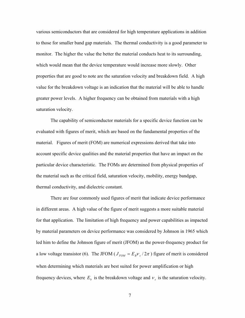
various semiconductors that are considered for high temperature applications in addition
to those for smaller band gap materials. The thermal conductivity is a good parameter to
monitor. The higher the value the better the material conducts heat to its surrounding,
which would mean that the device temperature would increase more slowly. Other
properties that are good to note are the saturation velocity and breakdown field. A high
value for the breakdown voltage is an indication that the material will be able to handle
greater power levels. A higher frequency can be obtained from materials with a high
saturation velocity.
The capability of semiconductor materials for a specific device function can be
evaluated with figures of merit, which are based on the fundamental properties of the
material. Figures of merit (FOM) are numerical expressions derived that take into
account specific device qualities and the material properties that have an impact on the
particular device characteristic. The FOMs are determined from physical properties of
the material such as the critical field, saturation velocity, mobility, energy bandgap,
thermal conductivity, and dielectric constant.
There are four commonly used figures of merit that indicate device performance
in different areas. A high value of the figure of merit suggests a more suitable material
for that application. The limitation of high frequency and power capabilities as impacted
by material parameters on device performance was considered by Johnson in 1965 which
led him to define the Johnson figure of merit (JFOM) as the power-frequency product for
a low voltage transistor (6). The JFOM ( πν 2/sBFOM EJ = ) figure of merit is considered
when determining which materials are best suited for power amplification or high
frequency devices, where is the breakdown voltage and bE is the saturation velocity. sν
7

Table 1.1. Summery of key intrinsic material parameters for various semiconductors. * An indirect bandgap is indicated with an I, and a direct bandgap by D (22).
Si GaAs InP GaP 4H-SiC GaN AlN Diamond
Energy Band Gap at 300K (eV)*
1.12 I 1.42 D 1.34 D 2.89 D 3.26 I 3.44 D 6.13 D 5.47 I
Dielectric Constant
13.2 (dc) 12.4 (dc) 9.6 (dc) 8.9 (dc) 11.1 (dc) 11.7 (dc) 9.14 (dc) 5.57 (dc) 10.9 (∞) 9.66 (∞) 6.7 (∞) 5.35 (∞)
Thermal Expansion 2.92 5.75 4.75 4.65 2.77 5.59 3.48 1.0 (10-6 K-1) Lattice Constant 3.189 a 3.111 a
8
(Å) 5.431 5.653 5.869 5.451 3.073 a 3.567 10.05 c 5.185 c 4.978 c
mc*/mo 1.18 0.063 0.077 0.21 - 0.22 0.40 0.2
mv*/mo 0.81 0.53 0.64 0.67 - 0.8 3.53 0.25
Electron Mobility 1450 8500 4600 160 1140 900 300 2200 (cm2/V·s) Hole Mobility 500 400 190 135 50 150 14 1600 (cm2/V·s) Saturation Velocity 1.0 1.0 - - 2.0 2.5 - 2.7 (107 cm/s) Breakdown Field 0.3 0.4 - - 3 5 - 10 (MV/cm) Thermal Conductivity 1.5 0.46 0.68 0.77 4.9 1.3 3.19 22 (W/cm·K) Melting Point (ºC) 1412 1238 1070 1749
Sublimes Sublimes 3025 3826 T>1827 T > 1300
In 1972, Keyes derived a figure of merit which provides a thermal limitation to the
switching behavior of transistors used in integrated circuits. A high value of the Keyes
figure of merit ( ) indicates materials that are best appropriate for
high speed digital ICs, where
2/1)/( κνσ sTFOMK =
κ is 4/1 . The KFOM is also a function of the thermal 0πε

conductivity, Tσ , which is responsible for setting the lower limit on the dimensions of a
device. In 1983, Baliga defined a figure of merit ( ) which defines material
parameters to minimize the conduction losses in power FETs, where
3BFOM EB κμ=
μ is the mobility.
High frequency systems have a non negligible amount of switching losses which are not
accounted for in the above figure of merit, making it only valid for low frequency
systems. In 1989, Baliga introduced the BHFFOM, a figure of merit for high frequency
devices. To improve efficiency of high frequency power systems, you want a high value
for BHFFOM. It is useful to consider all the FOMs when analyzing the impact of other
semiconductor materials on device performance. Semiconductor materials suited for
high frequency power switching applications should have a large critical breakdown
fields and should have high carrier mobilities. These properties result in minimizing
power loss in die area. Table 1.2 shows the values of the four figures of merit for several
common semiconductor materials with the values normalized to silicon for ease of
comparison.
There are other commonly used FOMs for semiconductor materials, such as the
FSFOM used to compare materials suitability for FET switching speed or the BSFOM
which is the equivalent FOM for bipolar transistors. There is also the FPFOM and
BPFOM for power handling of FET and bipolar transistors, respectively. The power
switching product of FET and bipolar transistors can be evaluated with the FTFOM and
BTFOM figures of merit. In all of the above mentioned FOMs, GaN and AlN have
numbers that far outreach the other conventional semiconductors, except diamond that
has higher values. However, diamond can not be controllably doped and is therefore not
useful as a device material at this time (7).
9

10
Table 1.2. Figures of merit for several semiconductor materials with the values normalized to silicon.
Si GaAs InP GaP 4H-SiC GaN AlN Diamond
JFOM 1 11 13 37 410 790 5120 5330 KFOM 1 0.45 0.72 0.73 5.1 1.8 2.6 31
BFOM 1 28 10 16 290 910 31,670 14,860
BHFFOM 1 16 6.6 3.8 34 100 1100 1080
All of the solid state advancements mentioned in this section paved the way for
the miniaturization of electronic and optical devices that are so prevalent today, and have
transformed the way consumers, industry, and the military rely on electrical device
components. Our modern military, with its heavy emphasis on technologically based
platforms and operations, increasingly depends on these materials each year.
Electronic and optoelectronic device manufacturers search for new materials that
can operate in harsher environments and in smaller devices. Advancements in
understanding the fundamental properties of a material will lead to the production of
more efficient devices with the characteristics required to meet the technical challenges
of current and future applications. Development of wide band gap (WBG)
semiconductor material characteristics and fabrication techniques can presumably thwart
many of the device failure mechanisms that result from inefficient material properties.
The advantages of WBG materials for high temperature, high power, and high
frequency devices are illustrated in the previous tables. They have much better FOM
values than that of Si. SiC has a better thermal conductivity than GaN, but not that of
AlN. AlxGa1-xN is a new material and all of its fundamental properties have not been

cataloged to date. However, it is presumable that the properties of AlxGa1-xN will start at
those of GaN for x equal to zero and migrate towards those of AlN as the Al mole
fraction is increased. What is still to be discovered is the relationship between how the
properties of GaN and AlN will change with increasing Al concentration. For example,
the energy band gap will increase in an almost linear fashion from 3.4 to 6.2 eV as the Al
mole fraction is increased from 0 to 1.
The Era Beyond Silicon
The push for electronics to perform in more caustic environments and in optical
devices that operate in the blue and ultraviolet regimes has increased research activity of
materials with a wide band gap due to their predicted performance in devices based on
the material properties illustrated in Table 1.1.
WBG semiconductors have many material properties, most of which are directly
related the wide band gap, that make them desirable for high temperature, high power,
and high frequency applications. For instance, the critical breakdown voltage is
proportional to the energy gap, , of the material, . Thus, the wider the
energy gap, the higher the breakdown voltage and the better capable the material is in
high power circumstances. WBG semiconductors have a high thermal conductivity and
therefore can conduct heat quickly away from themselves making them more reliable at
high temperatures and in high power situations. The internal electric field of a device
increases linearly as the device dimensions become smaller, thus the size of the device is
linked to the size of the energy gap. The wide band gap semiconductor by its nature
requires a large amount of thermal energy for the electrons in the valance band to be
excited in to the conduction band. This results in the material being able to function at
3/2gBR EV ∝gE
11
12
much higher temperatures before having a pronounced amount of thermal leakage current
that degrades device functionality. Other useful properties of WBG semiconductors are
large saturation velocities for high frequency operation and large cohesion energies
which make them chemically inert and resistant to radiation damage.
Silicon carbide has received a lot of consideration because of its high thermal
conductivity; however, it is not as good as group-III nitrides for optical devices due to its
indirect bandgap. Nitrides initially attracted attention after the commercialization of
bright blue light emitting diodes which were followed by the injection laser. They have
several advantages over other WBG semiconductors such as silicon carbide and diamond.
Nitrides have a direct bandgap, ability for both n- and p-type doping, for heterojunctions
conducive for device applications, and they can be grown epitaxially over a number of
substrates – which means that monocrystalline layers can be obtained over large surfaces.
In the beginning, the brightness of nitride based LEDs was too weak to surpass SiC blue
LEDs. In the late 1990s the brightness levels increased and bright violet, blue, and green
LEDs were fabricated with InGaN and GaN quantum wells.
In the early nineties, group-III nitrides were barely studied, but by the end of the
century GaN blue LEDs were taking over the market. The prospect of large payoffs led
the market and nitride based devices (LEDs, lasers, ultraviolet detectors, high
temperature, and microwave base electronics) were manufactured while their underlying
physics still remained a mystery (8). Group-III nitrides such as GaN, AlxGa1-xN, AlN,
and their alloys with indium are wide bandgap semiconductors that have direct band
gaps. They have many intrinsic material properties like high ionicity, very short bond
lengths, large energy gaps, low compressibility, high thermal conductivity, and high
melting temperatures that make them ideal for certain device applications (8).

13
Group-III nitrides are different from other III-V compounds such as GaAs and
GaP in many aspects. They have larger bandgap energies and therefore much larger
effective masses. Nitrides crystallize in the wurtzite structure in nature rather than zinc-
blende. They are found to be highly polar materials which can lead to strong
piezoelectric fields and even spontaneous polarization due to the low-symmetry wurtzite
structure (9).
Their wide band gaps lend to group-III-nitrides having low attenuation in the
near-infrared wavelength region and as semiconductors their refractive index can be
modified through carrier injection, making them prime candidates for use in fiber optic
communications (10). The fact that they work well in harsh environments, at high
temperatures, and with high power makes them good as tunable optical phased-array
(PHASAR) devices for optical communication. Research thus far has focused mainly on
the blue-UV wavelength applications. Their optical characteristics in the near infrared
region remain largely unknown and their potential application in fiber-optic
communication has just begun to be investigated. Rongqing Hui et al. developed an
optical waveguide device using GaN and AlxGa1-xN semiconductor materials (11). They
found that the refractive index of GaN decreases with wavelengths reaching 2.31 in the
1551 nm region. This is a much improved refractive index match with optical fibers than
InP, which is typically used. The refractive index of AlxGa1-xN was found to
monotonically decrease with increasing Al concentration, which will allow for precise
index adjustments critical in integrated optical circuit design. Group III-nitride
semiconductor materials are capable of making passive devices such as fixed wavelength
filters and splitters, but they may also enable active functionalities such as tunable
filtering and photonic switches (10).

14
Research advances into wide bandgap semiconductors composed of group-III
nitrides are of particular interest in applications which operate in high temperature, high
power, and high frequency environments, such as those associated with new hybrid cars
and the more electronic aircraft, warships, and modern ordnance systems (12). These
applications often require devices to operate under harsher conditions than those at which
smaller bandgap semiconductors can effectively function. Group-III nitride
semiconductor technology allows for the fabrication of UV light emitting diodes, laser
diodes, and solar blind cells. The technology allows for a multitude of other promising
devices such as the all white light emitting diode, which shows possibility of replacing
current lighting devices with solid state lighting applications offering superior energy,
endurance, and luminescence characteristics.
A New Material, AlxGa1-xN
GaN, AlxGa1-xN and AlN, have a direct bandgap that span the energy range from
3.4 eV to 6.2 eV and give rise to properties which show tremendous potential for current
and future electronic applications operating in high temperature, high power, and high
frequency environments. They can produce light from 200-360 nm and have been used
in lighting displays, green traffic signals, photo-catalytic processes, high resolution
optics, and UV solar blind photodetectors. Potential applications of these semiconductors
in opto-electronic devices include early missile plume detection, flame sensors, space-to-
space communications, solar-UV monitoring, biological and chemical detection systems,
water and air sterilization, and as a primary light source for phosphor-based white LEDs
(11). These new devices are more compact, energy efficient, rugged, and reliable than

15
devices made from conventional semiconductor materials, and can be relatively easy to
integrate with other electronics.
AlxGa1-xN is recognized as a promising material for optoelectronic devices in the
deep UV range. Highly conductive n and p-type alloys are necessary for device
applications. A major problem in obtaining highly conductive n-type Al rich material (x
>0.3) is the effect of compensation of electrons by cation vacancies and their complexes.
Suppressing such defects could greatly improve the conductivity of Al rich material (13).
The conductivity of undoped AlxGa1-xN decreases with increasing Al
concentrations and Al rich AlxGa1-xN alloys are normally found to be insulating. It has
been suggested that the decrease in conductivity is due to a transition of oxygen from a
shallow donor to a DX center. This same decrease in conductivity with increasing Al
mole fraction is found in Si-doped AlxGa1-xN. In this case, it is attributed to the
deepening of the Si donor level, compensation from acceptor-like defects, and an increase
in dislocation density. Highly conductive AlxGa1-xN materials are hard to come by due to
the incorporation of compensating acceptor-like defects such as Al vacancies or VAl-ON
complexes (14). Nakarmi et al. developed a growth technique that suppresses Al
vacancies and complexes and were able to grow a highly conductive Si-doped
Al0.7Ga0.3N epilayer (15). The sample had a reported resistivity of 0.0075 Ω·cm, carrier
concentration of 3.3x1019 cm-3, and mobility of 25 cm2/V·s. Although many devices have
already been reported using AlxGa1-xN, improvements in material quality and
conductivity are still needed.
Commercially available LEDs in the deep UV (λ < 340 nm) still face many
challenges and have low internal quantum efficiency. Jong Kyu Kim et al. have
developed a light emitting triode (LET) to try to overcome some of the challenges and

16
have produced a lighting device with increased quantum efficiency (16). AlxGa1-xN has
been used to make deep-ultraviolet light emitting diodes, and M. Khizar et al. found that
using a mircolens array increased the output power by 55% over conventional methods
(17). Their LED had a silicon doped Al0.6Ga0.4N active layer and produced light through
the sapphire substrate at a wavelength of 280 nm. Shakya et al. fabricated blue and UV
LEDs, and found that the degree of polarization of the band edge emission changes with
Al concentration (18). They suggest that the low efficiency of nitride UV LEDs is
partially related to this polarization property.
GaN based high electron mobility transistors (HEMTs) are the leading candidates
for high temperature and high power microwave applications due to GaN’s unique
material properties. The wide bandgap of GaN and its alloys leads to a high breakdown
voltage for GaN based HEMTs. A high breakdown voltage is crucial for power
performances of microwave power devices and circuits. There is still much work to be
done to increase device uniformity and minimize trapping centers in the material surface.
Researchers have tried a multitude of techniques to improve device performance.
An AlxGa1-xN/GaN (HEMT) fabricated with implanted Si ions was studied by
Haijiang Yu et al. (19). They activated the Si dopants in the source and drain region with
an ultra high temperature rapid thermal annealing technique that allowed them to anneal
at 1500 oC with 100-bar N2 overpressure for 1 minute without causing structural damage
to the material. The implanted HEMT device exhibited comparable contact resistance,
manifested DC, small signal and RF power performance comparable to HEMTs
processed by conventional fabrication. AlxGa1-xN/GaN HEMTs were fabricated by
Miyoshi et al. with Al concentration from 0.26 to 0.70 (20). They grew the structures by
metalorganic chemical vapor deposition on 100 mm sapphire substrate with uniformity of

17
±3% for all Al concentrations. They found that the sheet carrier concentration of the
AlxGa1-xN/GaN heterostructures increased with increasing Al content in the AlxGa1-xN
layers. They concluded that to achieve higher power densities for AlxGa1-xN/GaN
HEMTs, the materials should be grown with high Al mole fraction AlxGa1-xN. Jaesun
Lee et al. experimented with post annealing treatments on AlxGa1-xN/GaN HFETs and
found the heating treatment improved device breakdown voltage and device uniformity
as well as reducing trapping centers on the AlxGa1-xN surface (21).
AlxGa1-xN material exhibits many properties that make it an ideal candidate for
next generation electronic and optical devices. Although the research into this material is
still in the early stages of development, a wide variety of devices made from AlxGa1-xN
materials have already been fabricated in a number of research laboratories utilizing
many different Al mole fractions. A major drawback of an intrinsic material in device
performance is that the carrier density is too low and the resistivity is too high. This
problem can be solved by introducing dopants into the material that will act as donors
and acceptors. There are three major methods to accomplish this: in-situ doping,
diffusion doping, and ion implantation doping. For wide bandgap semiconductors,
diffusion doping is impractical due to the extended temperatures required for material
production. In-situ doping is widely used and has shown some major progress in creating
both n- and p-type materials. The ion implantation method is an alternative doping
technique and offers some advantages over in-situ doping. This method allows for a
selected area doping of the sample. It also offers advantages with respect to precise depth
and doping profiles, and device isolation.

18
Methodology
The goal of this research is to improve the functionality of everyday electronics
and optoelectronics by doing research at the material science level. AlxGa1-xN material
with Al concentrations from 0.1 to 0.5 are implanted with silicon ions and investigated as
a function of ion dose, anneal temperature, anneal time and Al concentration. The
objective was to find the conditions that most improved the carrier concentration as well
as the crystal quality of the material. Ion-implanted AlxGa1-xN has not been the subject of
intense investigation up to this point, as most of the research to date focuses on in-situ
doping.
In order to increase the conduction of AlxGa1-xN, silicon ions were implanted at
an energy of 200 keV at a 7º tilt to the material surface to reduce channeling effects. The
Si ions are amphoteric in the AlxGa1-xN crystal lattice but they exhibit a high tendency to
occupy donor positions. Three Si-implanted doses, 1x10¹⁴, 5x10¹⁴ and 1x1015 cm-2, were
investigated. A major draw back to the ion implantation technique is that the high energy
ions damage the crystal structure of the base material. The substrates must then undergo
a high temperature annealing treatment to restore the crystal structure and settle the
implanted ions into electrically active positions.
The Si-implanted AlxGa1-xN was annealed from 1100 to 1350 ºC for 20 to 40
minutes to determine the best possible conditions to achieve the highest activation
efficiency, mobility and a strong exciton peak. The annealing took place in nitrogen
ambient with all samples in a face-to-face configuration. These precautions were taken in
order to prevent out diffusion of nitrogen during the anneal process and also to protect the
sample surface.
19
Electrical material parameters were determined through temperature-dependent
Hall Effect and resistivity measurements, while low-temperature cathodoluminescence
measurements were used to investigate the optical properties. Together these
measurements can provide insight in the process of implantation activation and the defect
structures that result from it. This research effort aims to complete a comprehensive
investigation into the material properties of Si-implanted AlxGa1-xN as a function of Al
concentration, ion implantation dose, anneal temperature, and anneal time, with the goal
of enhancing the functionality of AlxGa1-xN optical and electrical devices.
II. Theory
In order to manipulate the fundamental properties of a given semiconductor
material, it is necessary to understand how these characteristics originate from the basic
structure of the material. Many of the properties discussed in Table 1.1 such as dielectric
constant, mobility, and electric breakdown field are a direct result of the material’s
structure. The arrangement and bonding of the atoms in a material determine how the
electrons will interact with one another. This chapter describes the connection between
the microscopic activities of electrons in a solid and the macroscopic properties they
manifest. The discussion in this chapter follows the development and presentation found
in Fellows’ dissertation (22).
Semiconductors are single crystal materials, which means that they have a high
degree of long range order (4). They have regular geometric periodicity throughout the
entire volume. The electrical and optical properties of the material are determined from
both the chemical composition and the arrangement of atoms. The two types of
semiconductors, elemental and compound, are made up primarily of elements from the
second through sixth columns of the periodic table. Elemental semiconductors consist, as
the name suggest, of only one type of atom from the fourth column of the periodic table,
such as Si and Ge. A compound semiconductor has two or more elements derived from
periodic table columns such as II, III, V, and VI. Compounds comprised of two elements
are referred to as binary compounds; those consisting of three elements are ternary alloys
and denoted as IIIxIII1-xV or IIxII1-xVI.
20

Crystal Structure of Solids
The atomic arrangement of atoms in solids was first investigated in 1913 by W.H.
and W. L. Bragg using their newly developed method of x-ray crystallography. They
discovered that the atoms in a solid have highly organized spatial qualities through the
study of the diffraction patterns produced by x-ray bombardment. The ordered structure
of the atoms is a result of a delicate balance of Coulomb forces that the atoms experience
due to their close proximity within the solid. As a result of these forces, the atoms
maintain a fixed distance from each other creating an ordered lattice formation (5). The
periodic nature of the single crystal allows for the entire lattice to be represented by a
fundamental unit cell which repeats to recreate the entire crystal structure. A lattice is
thus defined as the three-dimensional alignment of the crystal atoms. The arrangements
of atoms are described by Bravais lattices, which in mathematical terms is an infinite
array of discrete points with an arrangement and orientation that is exactly the same from
each point in the array (3). A Bravais lattice is one of fourteen unique unit cells that
represent the geometrical arrangement of the atoms in the solid. The 14 unique
arrangements include 1 triclinic, 2 monoclinic, 4 orthorhombic, 2 tetragonal, 1 hexagonal,
1 rhombohedral and 3 cubic lattice structures. Most semiconductor materials crystallize
in cubic or hexagonal crystal structure groups. Silicon and most III-V compounds
crystallize into the cubic form. Cubic lattices are highly symmetric and have three
classifications: simple (primitive), face-centered cubic (FCC), and the body-centered
cubic (BCC). The simple cubic has an atom at each of its eight corners, as does the BCC,
which also has an additional atom at its center. The FCC has atoms at each corner as
well as an atom at the center of each plane.
21

A crystalline solid is distinguished from other solids in two ways, first, by a
periodic arrangement of atoms, and second, by the binding forces that hold them together.
The binding energy of a material is the amount of energy required to break up a solid into
atoms and is interdependent on the type of bonds formed between the atoms. The
binding force then is a result of the quantum mechanical interaction between the
electrons. Electrons have a tendency to form filled outer electron shells and consequently
they will share, gain, or lose electrons in order to obtain a full valance shell. The two
types of bonding most prevalent in wide band gap semiconductors are ionic and covalent.
When atoms lose or gain electrons in their valance shell, the atoms become positively or
negatively charged ions which are then attracted to each other through Coulombic forces
leading to ionic bonding of atoms. Covalent bonding, on the other hand, results when
atoms share electrons with nearest neighbor atoms. They thus act as though they have
full valance shells. Most semiconductor materials exhibit this type of bonding. A
material determines which structure it will have based on the types of bonds that form
among the atoms.
In compound semiconductors, the chemical bonding is predominately covalent
and only slightly ionic, and therefore they have a tetrahedral bonding configuration which
results in most III-V compounds forming zincblende structures as opposed to wurtzite
structures. Both crystal arrangements are shown in Figure 2.1. A zincblende structure is
one that is made up of two interpenetrating FCC sublattices with each sublattice
containing only one kind of atom. Wurtzite materials have a primitive hexagonal Bravais
lattice structure with each plane of tetrahedra having mirror images of each other. The
physical arrangement of atoms in the lattice is the primary feature in determining the
22
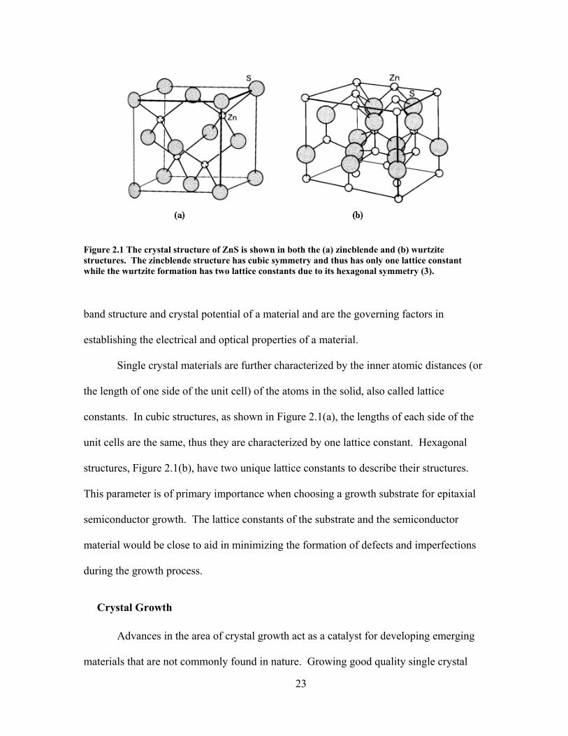
Figure 2.1 The crystal structure of ZnS is shown in both the (a) zincblende and (b) wurtzite structures. The zincblende structure has cubic symmetry and thus has only one lattice constant while the wurtzite formation has two lattice constants due to its hexagonal symmetry (3).
band structure and crystal potential of a material and are the governing factors in
establishing the electrical and optical properties of a material.
Single crystal materials are further characterized by the inner atomic distances (or
the length of one side of the unit cell) of the atoms in the solid, also called lattice
constants. In cubic structures, as shown in Figure 2.1(a), the lengths of each side of the
unit cells are the same, thus they are characterized by one lattice constant. Hexagonal
structures, Figure 2.1(b), have two unique lattice constants to describe their structures.
This parameter is of primary importance when choosing a growth substrate for epitaxial
semiconductor growth. The lattice constants of the substrate and the semiconductor
material would be close to aid in minimizing the formation of defects and imperfections
during the growth process.
Crystal Growth
Advances in the area of crystal growth act as a catalyst for developing emerging
materials that are not commonly found in nature. Growing good quality single crystal
23

material requires precise control over all aspects of the growth conditions, such as the
temperature of the source materials and growth substrate, the distance between the two,
the rotation speed of the substrate, and the cooling rate. Strict thermodynamic
equilibrium conditions must be maintained throughout the entire growth process. This
makes growth of compound semiconductors more difficult than elemental ones because
the stoichiometry (the correct chemical ratio of the compounds’ constituent elements)
must be maintained, while at the same time the thermal parameters to grow the perfect
crystal must be controlled. One component of the compound is generally more volatile
than the other, and is therefore more readily evaporated at high temperatures. In group
III-V semiconductors, this component is normally the group V element, leaving the
material group III rich if the growth conditions are not correct.
There are two types of growth methods for semiconductors: bulk growth and
epitaxial layer formation. In both growth types, it is important to minimize imperfections
and defects as well as the amount of unwanted impurities. The most common bulk
method is the Czochralski Method, in which a seed crystal is placed in contact with the
same material in liquid form and then slowly rotated as it is retracted from the liquid
solution. Bulk materials can be intentionally doped by adding a small amount of the
desired impurity into the liquid solution. After the growth, the boule can be trimmed to
the desired dimensions.
Epitaxy is a growth method of applying regularly oriented single crystals with
controlled thickness over a similar single crystal (called a substrate) which is generally
grown in bulk form. This growth method provides better control over purity, doping, and
thickness profiles. Epitaxial growth is used extensively for device manufacturing. It
24

utilizes a single crystal substrate as the seed and can be performed at much lower
temperatures than bulk growth. There are several methods of epitaxial growth including
vapor-phase epitaxy (VPE), liquid phase epitaxy (LPE), and molecular beam epitaxy
(MBE). For good quality epitaxial growth, it is essential that the substrate and the
material have a close lattice match.
If the lattice constants are not close, it can cause strain and defects in the material,
such as dislocations and vacancies (3, 20). A semiconductor material can be grown on a
substrate if the lattice constants of the two materials are close; however the
semiconductor will experience some type of strain as the lattice of the material tries to
adopt the lattice constant of the substrate. Pseudomorphic materials assume the lattice
constant of the substrate material. The chemical energy of the material, which defines its
lattice constant, and the strain energy which results from the new lattice constant both
contribute to the stability and quality of the crystalline formation. The strain energy
increases linearly with the epitaxial layer thickness and defines the critical thickness as it
approaches the value of the chemical energy. Below this thickness, the minimum energy
state of the epitaxial structure is dominated by strain. Above this thickness, the energy is
minimized by the formation of dislocation lines. The biaxial compression and tensile
strain are proportional to the extent of the lattice mismatch. The strain energy is reduced
through the formation of dislocations at the interface. Dislocations propagate upwards
and multiply as they go, forming threading dislocations. Aberrations to the crystal lattice
structure can affect the motion of the electrons within the crystal and have adverse effects
on the electrical and optical properties of the material.
25

Crystal lattices are not perfect in the real world and often contain defects and
imperfections which can have detrimental effects on the electrical properties of the
material. Lattice vibrations represent one type of disturbance, wherein the atoms do not
rest perfectly in the lattice position but actually vibrate around it. Point defects involve
single atoms and are comprised of vacancies, with an atom missing from a lattice site,
and interstitials, when atoms rest in between lattice sites. Point defects when grouped
together form complexes. A vacancy-interstitial complex is known as a Frenkel defect
and a line defect is one in which an entire line of atoms is missing. Dislocations are
defects in which atoms are misplaced from the lattice site.
The optical and electrical properties observed in a semiconductor can not be
completely explained by classical physics. To understand the movement of electrons in a
solid, it is important to consider what happens to the discrete energy levels of the
individual atoms as they are brought into close proximity to each other to form the crystal
lattice. No two electrons can have the same energy, therefore, the energy levels spread
into energy bands to accommodate all the electrons in the solid. The band theory of
solids explains the spreading of the energy levels by examining the wave functions of the
electrons. Significant outcomes to the theory are forbidden energy regions, the concept
of a hole, effective mass of the carriers, and the conduction properties (3).
Band Structure
The band theory of solids can be used to better understand how the above crystal
structure and residing defects can affect the fundamental properties of a semiconductor
material. To explain the experimentally observed properties of semiconductors, the free
electron model had to be expanded on. The free electron model of a solid is based on the
26

claim that conduction electrons are entirely free and do not interact with the other
electrons or the positively charged ion cores. In semiconductors however, there is a
periodic potential with the periodicity of the lattice that arises from the regular
arrangement of the ion cores from the host atoms. It is the quantum mechanic interaction
between the electrons and the periodic potential of the lattice that gives rise to the
electronic band structure of solids.
To form the crystal lattice of a solid, atoms come in close contact with each other
which enables the wave functions of the electrons to interact and cause the discrete
energy levels of the individual atoms to split in order to accommodate the electrons from
neighboring atoms. This splitting is a direct result of the fermionic nature of the
electrons. The electrons interact with other electrons in the solid and also the ion cores
that are positioned periodically at the lattice sites. The energy band structure for a solid
is determined by the interactions of the electrons with the periodic potential of the lattice.
The electrons in a solid can be considered as core electrons (those tightly bound to the
atomic nuclei), and valance electrons (those less bound due to the effects of screening
from the inner electrons). The microscopic nature of electrons in a solid is described in
terms of this electronic band structure. The best way to visualize the electron in the
lattice is to consider an infinite number of quantum wells with a periodic potential, V0.
When the energy of the electron, E, is less than the potential energy, E < V0, the electron
is bound to the atom. On the other hand, when the energy is greater than the potential, E
> V0, the electron is free to move around the crystal and to participate in conduction.
Schrödinger’s equation has to be solved in each region to determine the energy levels of
the electron. However, since the valance electrons can be considered as nearly free
27

electrons, their approximate energy levels can be determined by considering the case of a
free electron.
This is simplest case to solve because the free electron does not experience any
outside potential forces from either the ion cores or other electrons. The energy levels of
the free electron are determined by solving Schrödinger’s equation, Equation 2.1, with
the potential being equal to zero
)()()(2
)( 2
0
rErrUm
rH vvrhr ψψψ =⎟⎟⎠
⎞⎜⎜⎝
⎛+∇−= , (2.1)
Hwhere is the Hamiltonian operator, h is the reduced Plank’s constant, is the mass
of an electron,
0m
)(rU r is the potential, E is the energy, and )(rrψ is the wave function
describing the motion of the electrons. For a free electron in three dimensions, the
solution to Schrödinger’s equation are plane waves of the form
rkik er
rrr ⋅=)(ψ , (2.2)
where is the electron’s wave vector and kr
rr is the electron’s position vector. The
eigenvalues that satisfy the eigenstates for Equation 2.1 are then given by
0
22
2)(
mkkE hr
= . (2.3)
The variation of energy as a function of the wave number is known as the dispersion
relation. Electrons are not completely free, thus the values of k are dependent on the
periodicity of the lattice by
nL
k π2= , (2.4)
where n is required to be an integer and L is the lattice constant. This relationship dictates
that not all values of k will lead to acceptable electron wave functions. Not all energies
28
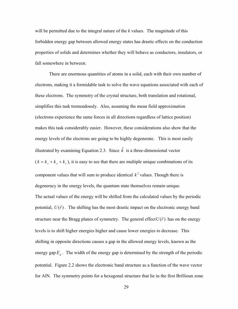
will be permitted due to the integral nature of the k values. The magnitude of this
forbidden energy gap between allowed energy states has drastic effects on the conduction
properties of solids and determines whether they will behave as conductors, insulators, or
fall somewhere in between.
There are enormous quantities of atoms in a solid, each with their own number of
electrons, making it a formidable task to solve the wave equations associated with each of
these electrons. The symmetry of the crystal structure, both translation and rotational,
simplifies this task tremendously. Also, assuming the mean field approximation
(electrons experience the same forces in all directions regardless of lattice position)
makes this task considerably easier. However, these considerations also show that the
energy levels of the electrons are going to be highly degenerate. This is most easily
illustrated by examining Equation 2.3. Since kr
is a three-dimensional vector
( ), it is easy to see that there are multiple unique combinations of its
component values that will sum to produce identical values. Though there is
degeneracy in the energy levels, the quantum state themselves remain unique.
zyx kkkk ++=
2k
The actual values of the energy will be shifted from the calculated values by the periodic
potential, )(rU r . The shifting has the most drastic impact on the electronic energy band
structure near the Bragg planes of symmetry. The general effect )(rU r has on the energy
levels is to shift higher energies higher and cause lower energies to decrease. This
shifting in opposite directions causes a gap in the allowed energy levels, known as the
energy gap . The width of the energy gap is determined by the strength of the periodic
potential. Figure 2.2 shows the electronic band structure as a function of the wave vector
for AlN. The symmetry points for a hexagonal structure that lie in the first Brillioun zone
gE
29
are denoted on the k axis, the most important of which are the Γ point or center and the L
and K points. These symmetry points as they relate to the crystal structure are illustrated
in Figure 2.3 which shows the first Brillioun zone for the hexagonal AlN structure.
These symmetry points are more relevant when considering optical transitions.
Figure 2.2. An energy band diagram for AlN which illustrates a variety of points of symmetry within the first Brillioun zone. The conduction band minimum and the valance band maximum both occur at the Γ point in k-space (77).
30
The motion of the electrons in the allowed bands is generally explained through
the consideration of only two bands, the valance band (VB) and the conduction band
(CB). At a temperature of absolute zero the electrons occupy their lowest energy
configurations, the highest energy band that the electrons fill or partially fill is known as
the valance band and the next highest band containing no electrons is the conduction
band. The difference in energy between these two bands is the energy band gap for the
material. The size of the band gap determines the material’s fundamental electrical
properties. A solid material then can be divided into three types: a conductor, an
insulator, or a semiconductor depending on the magnitude of the energy gap. For metals
the valance and conduction bands overlap so that there are always electrons available to
partake in conduction. Insulators, on the other hand, have a large energy band gap (Eg >
6 eV) requiring the electrons in the valance band to obtain a considerable amount of
energy or extreme temperatures for the electrons to be able to move to the conduction
band, thus insulators do not conduct electricity. Semiconductors are so named based on
their ability to behave as both a conductor and an insulator. Semiconductors have an
energy gap in the range of less then 1 eV to 6 eV, which allows them to act as both an
insulator and a metal depending on the conditional settings. Semiconductors are
distinguished from other solid materials by the behavior of their electrons and the gaps in
their electronic spectra. Valance electrons, due to the effects of screening, experience
only a weak periodic potential and can be considered free electrons (5). However, at
absolute zero (0 K) semiconductors behave as insulators. As the temperature is increased
(T > 0 K), the electrons will gain sufficient thermal energy to move to the conduction
band, and contribute to the conduction.
31

Figure 2.3. The first Brillioun zone of the hexagonal crystal structure of AlN showing various points of symmetry of the crystal structure (77).
Another important aspect to the energy diagrams is whether the band gap is direct
or indirect. For a direct band gap, the valance band maximum and the conduction band
minimum occur at the same point in k-space. For an indirect bandgap, the VB maximum
and the CB minimum do not occur at the same point in k-space, i.e. the conduction band
minimum is not at . This results in a phonon being required for optical transitions as
a result of the conservation of crystal momentum. Materials with a direct band gap are
more ideally suited for optical devices.
0=k
Semiconductor materials are not charged so that when an electron moves into the
conduction band it must leave behind a positively charged state to maintain the charge
32
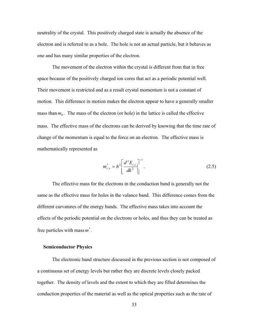
neutrality of the crystal. This positively charged state is actually the absence of the
electron and is referred to as a hole. The hole is not an actual particle, but it behaves as
one and has many similar properties of the electron.
The movement of the electron within the crystal is different from that in free
space because of the positively charged ion cores that act as a periodic potential well.
Their movement is restricted and as a result crystal momentum is not a constant of
motion. This difference in motion makes the electron appear to have a generally smaller
mass than . The mass of the electron (or hole) in the lattice is called the effective
mass. The effective mass of the electrons can be derived by knowing that the time rate of
change of the momentum is equal to the force on an electron. The effective mass is
mathematically represented as
0m
1
2,
22*
,
−
⎥⎥⎦
⎤
⎢⎢⎣
⎡=
dkEd
hm vcvc . (2.5)
The effective mass for the electrons in the conduction band is generally not the
same as the effective mass for holes in the valance band. This difference comes from the
different curvatures of the energy bands. The effective mass takes into account the
effects of the periodic potential on the electrons or holes, and thus they can be treated as
free particles with mass . *m
Semiconductor Physics
The electronic band structure discussed in the previous section is not composed of
a continuous set of energy levels but rather they are discrete levels closely packed
together. The density of levels and the extent to which they are filled determines the
conduction properties of the material as well as the optical properties such as the rate of
33

absorption and emission. Current is due to a flow of charged particles in a material, so it
is important to know the density of electrons or holes. The number of carriers is directly
proportional to the number of available states. The density of states is defined as the
number of states per unit volume and unit energy ( ). This is
easiest to do in k-space using the energy-momentum relation to give the density of states
in terms of the energy.
)/)(/1()( 3 ENLEg ∂∂=
)(kEr
From examining Equation 2.3, it can be seen that forms spheres of constant
energy in three dimensional k-space. The density of discrete energy levels per unit
volume per unit energy is determined by first considering the smallest volume on the
sphere that can contain one energy level. Since nk 2π= L/ , the smallest possible volume
in k-space is then . Accounting for spin degeneracy, the volume becomes
. Dividing the density of states by this volume yields per volume measures.
Consider the number of states in a generic volume in k-space with surface area
multiplied measured outward from the surface. The change in the k-direction is
equivalent to the reciprocal of the derivative of
33 /8 Lπ
33 /4 Lπ
)(ESkΔ
nkΔ
)(kEr
with respect to k. The density of
allowed states as a function of energy for both the valance band and the conduction band
is defined as
23
*,32
,3, )(
||2)(4
1)( vcvc
surface kvc m
EEkE
dsEghππ
−=
∇= ∫ (2.6)
with the integral over constant energy surfaces in k-space. Integrating over the entire
constant energy surface, the number of states per energy per unit volume as a function of
the effective mass is shown also in Equation 2.6. The density of states strictly describes
34

the number of available levels but not how the electrons are distributed in these levels.
The Fermi-Dirac distribution function describes the allocation of electrons among the
available . The Fermi-Dirac distribu
energy levels tion is shown below
1exp
1)(+⎥
⎦⎣ TkB
where is the Fermi energy that is normally about TkB3 lower than the conduction
band, Bk is the Boltzman constant, and T is the temperature. The carrier concentration
involves the integral of the product of the Fermi Dirac Function and th
⎤⎢⎡ −
=EE
EfF
FD , (2.7)
e density of state
function. The number of electrons occupying these states is given by
. (2.8)
nly
zman distri
FE
∫∞
= dEEfEgTn )()()(cE
Sometimes it is simpler to use the Maxwell-Boltzman distribution, which differs o
slightly but significantly simplifies the math required to solve the integral in
Equation 2.8. The Maxwell-Bolt bution can be used instead of the Fermi-Dirac
distribution in the regime where TkE B>>Δ holds true, where EΔ is difference in
between the conduction band and the Fermi level. In this approximation the two
dist
energy
ributions yield close to the same results. The Maxwell-Boltzman distribution is given
by
⎥⎦⎣ TkB
Solving Equation 2.8 using the )(Ef MB yields the foll
⎤⎢⎡ −
=EE
EfF
MB
exp
1)( . (2.9)
owing for the number of electrons
the conduction band as a function of temperature. in
35

⎥⎦
⎢⎣⎦⎣ TkB2 2hπ
For a non-degenerate semiconductor, the coefficient to the exponent represents
the upper limit of the volume concentration of the conduction electrons and is referred to
as the effective density of states. The concentration of holes in the valance band can b
determined similarly and is shown in Equation 2.11. In intrinsic semiconductors, the
concentrations of electrons and holes are equal and their product determines
⎤⎡ −⎥⎤
⎢⎡
=EETkmTn cFBc exp1)(
23
*
(2.10)
e
the intrinsic
carrier concentration; a fundamental material constant for all temperatures.
⎥⎦
⎤⎢⎣⎦⎣ TkB2 2hπ⎡ −
⎥⎤
⎢⎡
=EETkm
Tp FvBv exp1)(23
*
(2.11)
The intrinsic carrier concentration is calculated as follows
⎥⎦⎣
⎥⎦⎢⎣ TkBvci 22 2hπ
The intrinsic carrier concentration is a fundamental material parameter that
depends only on the effective mass and the energy gap. For a pure semiconductor, the
intrinsic carrier concentration is equal to th
⎤⎢⎡ −⎤⎡==
ETkmmTpTnTn gB exp)(1)()()(23
43
** . (2.12)
e electron concentration and also the hole
concentration at any given temperature.
Effe
nd
on
electrical properties can be manipulated in an accurate and reliable way. The main
cts of Impurities
A perfect crystal is something that only exists as an idea and can rarely be fou
in nature. Impurities in semiconductors have been found to enhance the conducti
properties of the material. By introducing impurities in a controlled manner, the
36

properties that are of interest are conductivity, carrier concentration, and mobility. These
three properties are related through Equation 2.13.
)( pn pne μμσ += . (2.13)
Here e is the charge of the electron, n and p are the electron and hole carrier
concentrations, and and nμ pμ represent the mobility for the electrons and holes,
respectively.
Semiconductor materials are unique in that they exhibit conduction from both
electrons and holes. In an intrinsic semiconductor, the concentration of electrons and
holes are equal and their product defines the intrinsic carrier concentration, known as the
law of mass action, as defined in Equation 2.12. The intrinsic carrier concentration is a
fundamental constant of the crystal for all temperatures. In extrinsic semiconductors, the
impurity atoms can donate electrons or holes to the crystal, and in this case the values of
n and p are no longer equal. However, the law of mass action still holds, so that as the
electron carrier concentration increases, the hole concentration must correspondingly
decrease and vice versa. The type of conduction taking place in the material is
determined by whether electrons or holes serve as the majority carriers. In n-type
material, the majority carriers are electrons, while in p-type material the majority carriers
are holes. A small amount of impurity atoms can have profound effects on the
conduction of the material.
Semiconductors form closed valance shells through covalent bonding with their
nearest neighbors. When impurity atoms from neighboring columns in the periodic table
occupy a lattice site of the host crystal, they attempt to form all the bonds the crystal's
atoms would have created. Sometimes the impurity atoms will complete all the bonds
37

but have one or more extra electrons, such as case when silicon ions (column IV) replace
Ga (column III) atoms in a GaN crystal. These “extra” electrons are then free to join the
conduction. In this case, the impurity ions are referred to as donors. On the other hand,
the impurity ions may not have enough electrons to complete all the bonds (Si on an N
site) and thus create holes that are readily available to participate in the conduction in the
valance band. Impurity ions of this type are called acceptors. Impurities that can act as
both acceptors and donors in a material, such as Si in GaN, are called amphoteric
dopants. Silicon ions normally tend to occupy gallium sites, and act as donors when
introduced into a GaN crystal.
The ionization energy of the impurity ions can be estimated by comparing the
isolated impurity atom to the hydrogen model of an atom and seeing that they represent
the same circumstance. The ionization energy can then be approximated by using the
energy levels for the hydrogen model as shown in equation 2.14
eVenm
E 06.132 22
40 −=−=κh
for n = 1 (2.14)
Here κ = 4πε0, where ε0 is the permittivity of a vacuum. In order for this equation to be
valid for impurity atoms, m0 must be replaced by the effective mass and ε0 must be
replaced with the relative dielectric constant of the semiconductor material.
The impurity ions create energy levels within the forbidden band gap region.
Donor levels can be shallow, forming only a few meV below the conduction band for
non-wide band gap semiconductors. Acceptor levels similarly form within a few meV
above the valance band. It is possible, however, for energy levels to be deep within the
band gap region. Shallow donors and acceptors are normally thermally ionized at room
temperature, meaning the electrons (holes) have gained enough thermal energy to move
38

into the conduction (valance) band and participate in the conduction. Shallow and deep
donor and acceptor energy levels in units of electron volts for GaAs are shown in
Figure 2.4. The number of free carriers in a semiconductor crystal can be calculated by
looking at the charge balance equation. The overall net charge of the crystal is zero,
therefore the charge from the positive ions must be equal to the charge of the negative
ions. This is expressed mathematically in Equation 2.15, where n and p are the
concentrations of electrons and holes already taking part in the conduction. The
concentration of unionized donors and acceptors is given by and , and
represents the total concentration of the unionized electron and hole impurities,
respectively (3).
dn ap adN ,
)()( ddaa nNppNn −+=−+ . (2.15)
Solving this equation for and yields an equation proportional to the ionization
energy of the impurity.
ap dn
1/)( += − TkEE
v
aa BaFeg
Np (2.16)
and
1/)( += − TkEE
c
dd BFaeg
Nn (2.17)
where accounts for the degeneracy. These equations, along with experimental data o
the carrier concentrations as a function of temperature, can be used to determine the
ionization energy of the impurity atoms. This data curve can be fitted to extract the
values of , , and and is known as an Arrhenius plot. The extracted values for
the activation energy can be lower than the actual values due to screening effects.
vcg , f
aN dN aE
39

Figure 2.4. Impurity donor and acceptor levels in eV for various atoms in GaAs (71, 23).
When the impurity atom is embedded with the pure semiconductor, the binding
energy is significantly reduced. The binding energy of an electron to an impurity atom is
much smaller compared to the band gap. This makes it easier to thermally ionize the
donor electrons to produce conduction. The conduction band can be approximated by a
parabola. The conductivity of the material includes both the conduction due to electrons
and holes as shown in Equation 2.13.
Intentional introduction of impurities can benefit the conduction up to the point at
which the doping density becomes so large that the impurity atoms are separated by less
than the Bohr radius. At this point the material undergoes a Mott transition and begins
acting like a metal and control over the conductivity of the material is lost. The defining
equation for the critical doping density is given in Equation 2.18, where . A rr πεκ 4/1=
40

high level of doping can result in impurity band formation, band tailing, band filling and
other effects that inhibit the control of the material's conduction properties.
3
9*,
0 1029.53
−
−
⎥⎥⎦
⎤
⎢⎢⎣
⎡×⎟
⎟⎠
⎞⎜⎜⎝
⎛= cm
mm
Nvc
rcrit
κ (2.18)
When the doping concentration is much less than the critical concentration, the
impurity atoms are isolated such that their wave functions do not overlap and form
discrete energy levels. As the doping concentration approaches the critical limit, the
wave functions of the donor electrons begin to overlap, forming an impurity energy band.
If the critical doping density is exceeded, the impurity band merges with the conduction
band or valance band depending on which type of impurity band was created.
The spatial distribution of impurity atoms is generally random, causing random
fluctuations at the band edges, known as band tailing. As the impurity concentration
grows, free carriers begin to occupy states above the bottom of the conduction band.
This is known as band filling, and is common in highly doped, highly degenerate
semiconductors (22).
There are several techniques to incorporate the dopants in the host material.
These include diffusion doping, in-situ doping, and ion implantation doping. Diffusion
doping takes place at high temperatures with the material placed in a gaseous atmosphere
of the desired dopant. This is not feasible for nitrides due to the low evaporation
temperature of nitrogen. In-situ doping (doping during growth) of group-III nitrides has
shown much progress in the last few decades with both n and p-type GaN and low Al
concentration AlxGa1-xN alloys. However, there is still much progress to be made in this
41

42
area with regard to limiting the number of defects caused by the dopant incorporation. In-
situ doping has become a viable method of doping a semiconductor material; however
this method does not allow for selective area doping. Ion implantation has advantages
over other methods because it is quick and cost effective and allows for doping of
specific material areas as well as the aforementioned advantages with respect to device
isolation and precise depth and doping profiles.
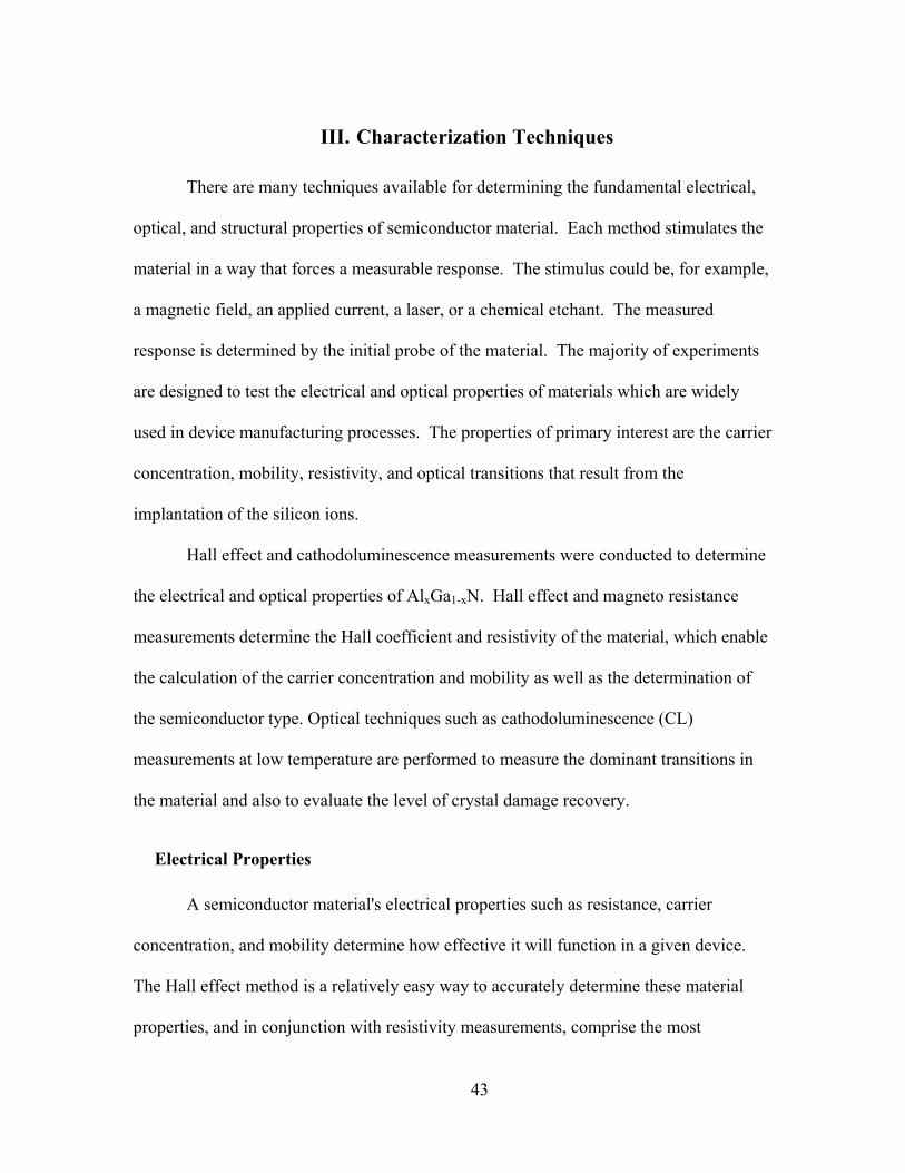
III. Characterization Techniques
There are many techniques available for determining the fundamental electrical,
optical, and structural properties of semiconductor material. Each method stimulates the
material in a way that forces a measurable response. The stimulus could be, for example,
a magnetic field, an applied current, a laser, or a chemical etchant. The measured
response is determined by the initial probe of the material. The majority of experiments
are designed to test the electrical and optical properties of materials which are widely
used in device manufacturing processes. The properties of primary interest are the carrier
concentration, mobility, resistivity, and optical transitions that result from the
implantation of the silicon ions.
Hall effect and cathodoluminescence measurements were conducted to determine
the electrical and optical properties of AlxGa1-xN. Hall effect and magneto resistance
measurements determine the Hall coefficient and resistivity of the material, which enable
the calculation of the carrier concentration and mobility as well as the determination of
the semiconductor type. Optical techniques such as cathodoluminescence (CL)
measurements at low temperature are performed to measure the dominant transitions in
the material and also to evaluate the level of crystal damage recovery.
Electrical Properties
A semiconductor material's electrical properties such as resistance, carrier
concentration, and mobility determine how effective it will function in a given device.
The Hall effect method is a relatively easy way to accurately determine these material
properties, and in conjunction with resistivity measurements, comprise the most
43

commonly used characterization techniques utilized to determine a material’s electrical
properties in the semiconductor industry.
Hall Effect Theory
The Hall Effect theory was discovered in 1879 when Edwin H. Hall, an American
physicist, discovered that a small transverse voltage was generated across a thin metal
strip in the presence of an orthogonal magnetic field. The discovery of this transverse
voltage, or Hall Voltage, enabled the independent calculation of the mobility and the
carrier concentration of the material which was only accomplished up to that time
through difficult measurements. Van der Pauw, in 1958, made the theory more
experimentally testable when he showed that the shape of the measured sample was not a
factor and only required that the sample be simply connected and exhibit highly ohmic
point contacts on the periphery of the material (23).
According to the Hall Effect theory, electrons moving in a specimen find
themselves subject to the Lorentz Force when in the presence of a perpendicular
magnetic field. Hall Effect measurements are conducted by placing a sample in a
magnetic field that is orthogonal to its surface as illustrated in Figure 3.1. A current is
applied to the material so that the charged carriers move in the x direction. The moving
charges induce an internal electric field in the material, which deflects the charges toward
the edges of the material. Positively charged particles (holes) move to one edge, and the
negatively charged particles (electrons) move to the opposite edge. This particle
movement is the result of the charge carriers being subject to the Lorentz Force, which is
normal to the magnetic field. The Lorentz Force is given by
44
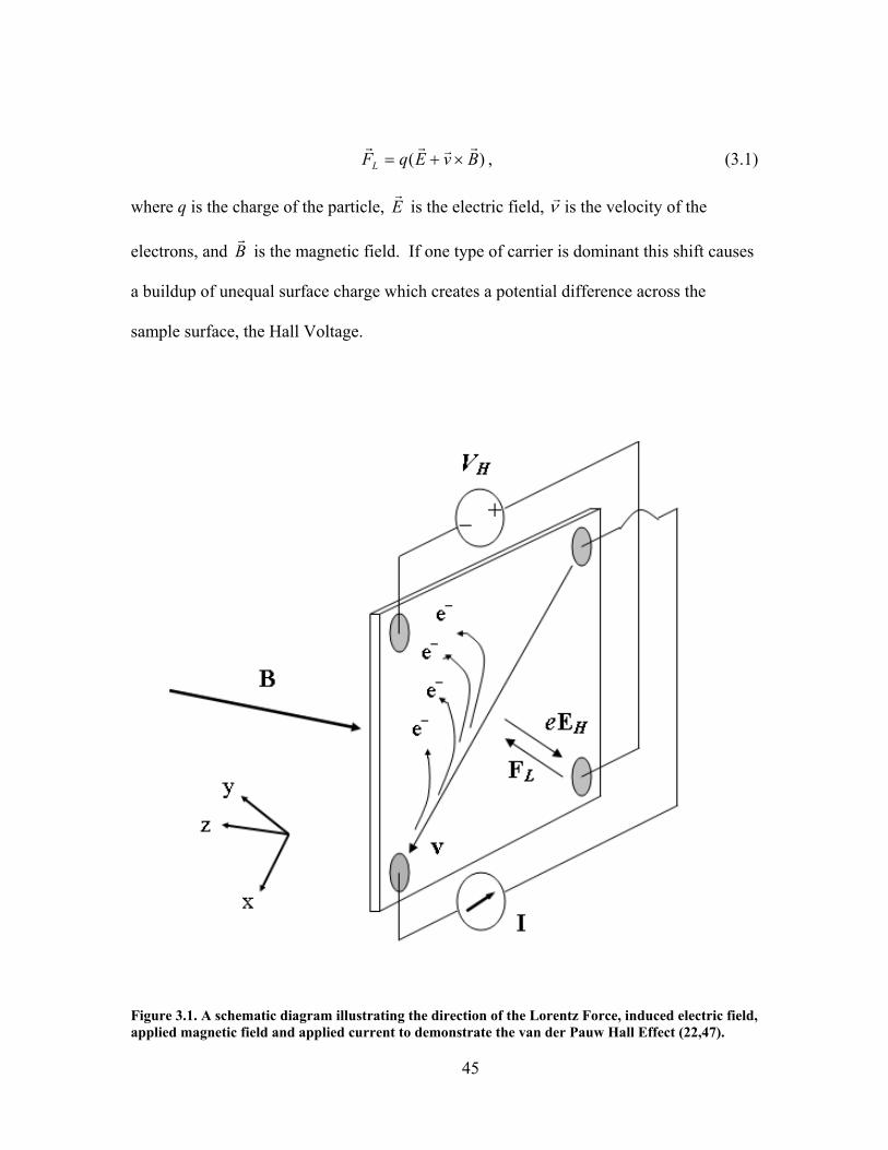
)( BvEqFL
rrrr×+= , (3.1)
Er
where q is the charge of the particle, is the electric field, νr is the velocity of the
electrons, and Br
is the magnetic field. If one type of carrier is dominant this shift causes
a buildup of unequal surface charge which creates a potential difference across the
sample surface, the Hall Voltage.
Figure 3.1. A schematic diagram illustrating the direction of the Lorentz Force, induced electric field, applied magnetic field and applied current to demonstrate the van der Pauw Hall Effect (22,47).
45
This generated transverse voltage will therefore have a different sign for n and p-type
materials. Solving the cross product in Equation 3.1, it can be seen using Figure 3.1 that
the Lorentz Force equation becomes
zxyy BqvqEF += (3.2)
The system will strive for equilibrium and therefore the Hall Voltage will grow until it
becomes equal to the Lorentz Force. When this occurs, is zero and equation 3.2 can
be simplified to
yF
zxy BvE −= (3.3)
The current density which is defined in equation (3.4) can be solved for the velocity and
substituted into the electric field equation (3.3), rendering the equation to experimentally
measurable quantities.
H
xx nqr
Iv =Hxx rnqvI = . (3.4) →
The Hall factor is represented by and denotes the Hall to drift mobility ratio which is
usually approximated to be one, but can vary between one and two. This estimation
causes the Hall Effect measurements to often underestimate the values of the carrier
concentration. The substitution of
Hr
xν into equation (3.3) yields an equation for the electric
field in terms of the Hall coefficient, applied current, and applied magnetic field that is
given by
zxHH
zxy BJR
nqrBI
E == . (3.5)
The above equation is then used to define the Hall voltage. The Hall voltage is the
product of the generated electric field and the width of the sample, w.
46

wBJRwEV zxHyH == . (3.6)
The Hall voltage, being a measurable quantity, is used to calculate the Hall coefficient.
Rearranging equation (3.6) to solve for the Hall coefficient in all experimentally
measurable values yields
wBJVR
zx
HH = . (3.7)
The magnitude of the Hall voltage is inversely proportional to the carrier concentration
and the sign of this voltage indicates the dominant carrier type. For electron
conductivity, the Hall coefficient is negative, and the coefficient is positive for hole
conduction. This value, along with the resistivity of the material, is needed to determine
the carrier concentration and mobility. These relationships are shown as equation (3.8).
s
HH
Rρ
μ =H
Hs qR
rN = and . (3.8)
Temperature-Dependent Hall (TDH) measurements provide carrier concentrations
and mobility values as a function of temperature. At low temperatures the shallowest of
impurities should freeze, leaving the material highly resistive. If the material is highly
degenerate, TDH measurements will reveal this degenerate layer at low temperatures via
the mobility and carrier concentration will be temperature independent. The impurity
ionization energies are extracted by fitting the temperature-dependent carrier
concentration data. The samples are placed in a vacuum during the TDH measurements
to prevent condensation or oxidation, which would be damaging to the sample and
adversely affect measurement accuracy (7).
47

Hall Effect Measurements
The Hall effect measurements are made with an automated Lake Shore 7505
system. A diagram of the system is provided in Figure 3.2. The samples are placed on
Janis vacuum heads designed for low (10-320 K) and high temperature (300-700 K)
measurements which are placed between two coil magnets that are capable of producing
up to a 7 kG magnetic field. All measurements are done in a 5 kG field. Current is
supplied to the sample with a Keithley 220 current source and the generated Hall Voltage
is measured using a Keithley 2182 nanovoltmeter. Lake Shore Hall program version 3.3
automates the process and records the resisitivities and Hall data. Exact operating
procedures can be found in appendix A.
There is a separate system for high and low temperature measurements. The
systems are identical except for the Janis vacuum head. The high temperature system
uses pressure contacts to make contact with the material while the low temperature
system must use gold wires connected with indium solder.
Hall Measurements provide only average carrier concentration and mobility
values over the entire conducting thickness. A total of 8 current-voltage pair
measurements are averaged to calculate the sheet resistivity. Four current-voltage pair
measurements taken under forward and reverse magnetic fields are averaged to calculate
the Hall Coefficient. The Hall measurements are also used to determine the activation
efficiencies of the implanted samples. The following relations are used:
i
s
Drn
A = and ⎟⎟⎠
⎞⎜⎜⎝
⎛−=
TkE
rB
ai exp , (3.9)
where A is the activation efficiency, is the sheet carrier concentration, D is the sn
48

Figure 3.2. A schematic diagram of the LakeShore 7505 automated Hall measurement system for carrier concentration, resistivity, and temperature-dependent measurements. The board for room temperature measurements is illustrated and the system is also equipped with a low temperature and high temperature operating head.
49

implanted ion dose, is the ionization rate, and is the acceptor or donor ionization
energy.
ir aE
From these relations it can be seen that as the temperature rises more impurities
become ionized causing the carrier concentration and mobility to change. For wide
bandgap semiconductors the energy levels are deeper and thus require higher
temperatures to activate these levels.
Optical Properties
The optical properties of the semiconductor material give insight into the
dominant transitions, determination of the band gap, and the quality of the crystal
structure. Materials with strong emission in a short wavelength band make for good
optical device components in the UV and blue spectral regions. All the optical
measurements in this study were performed using cathodoluminescence measurement
techniques at low temperatures (T< 10 K).
Optical Theory
The discussion in this section follows the development and presentation found in
Fellows’ dissertation (22). When a solid is supplied with sufficient energy, it will emit
photons as well as thermal radiation. The type of luminescence depends on the excitation
source and the variance of the material’s bandgap. Some examples of optical excitation
are photoluminescence (PL, excitation by photons), cathodoluminescence (CL, excitation
by energized electrons) and electroluminescence (EL, excitation by an electric field).
There are two types of luminescence that semiconductors exhibit: fluorescence and
phosphorescence. Fluorescence is the emission of photons due to a direct transition from
50

excited state to ground state, while phosphorescence utilizes intermediate transitions so
that the luminescence persists after the excitation source is terminated. Materials that
have this type of luminescence are generally referred to as phosphors (24).
Semiconductors normally exhibit fluorescence.
Luminescence in semiconductors can be described in terms of the radiative
recombination of electron-hole pairs. The wavelength of the luminescence is given by
Ehch Δ== λν / , where h is Plank's constant, ν is the frequency, c is the speed of light,
λ is the wavelength, and EΔ is the initial energy, minus the final energy, , in the
transition.
iE fE
The electron-hole pairs relax to equilibrium through a succession of interactions
with defect and impurity levels within the bandgap that eventually leads to
recombination. This may include transitions from the valence to conduction band, or
those levels within the band gap, such as donor and acceptor levels. The most common
radiative transitions are illustrated in Figure 3.3.
Luminescence spectra can be collected for all radiative transitions that occur
between two energy levels. The transition labeled as (a) in Figure 3.3 is a band-to-band
transition and is generally dominant at room temperature. The energy of this transition is
given by
gvc EEEh =−=ν , (3.10)
where is the energy gap. The free exciton (FE) transition is shown as (b) in the above
figure. In this case the electron is bound to the hole through coulombic forces. The
energy of this transition is the bandgap energy minus the binding energy of the two
particles, and its mathematical representation is given in Equation 3.11.
gE
51

Figure 3.3. A two dimensional illustration of the most common radiative transitions that take place in semiconductors. The transitions shown are: the band-to-band transition (a), the free exciton transition (b), the neutral donor free hole recombination (c), a free electron transitioning to a neutral shallow acceptor (d), and the donor acceptor transitions for shallow and deep states (e) and (f) respectively (22).
2
4*
2 hκν qmEh rg −= (3.11)
where is the reduced effective mass of the exciton, q is the charge, and κ is equal to *rm
, whererπε4 rε is the reduce dielectric constant. Transitions (c) and (d) are the similar
transitions in reverse. Transition (c) shows the transition from an electron on a neutral
donor recombining with a free hole (D0, h), while (d) illustrates the recombination of a
52

free electron in the conduction band and a hole on a shallow neutral acceptor (e, A0). The
energy for these transitions is given by
adg EEh ,−=ν . (3.12)
The last two transitions in the diagram are extremely important and are the same
transition; only the depth of the acceptor and the donor levels change. They are the
donor-acceptor pair (DAP) transitions, where an electron on a shallow donor recombines
with a hole on a shallow neutral acceptor, or as seen in (f) where an electron in a deep
donor recombines with a hole in the deep acceptor. The energy of this type of transition
is given by
rqEEEh adg κ
ν2
+−−= , (3.13)
where r is the separation distance between the donor and the acceptor. The last term in
the equation represents the electrostatic energy gained as the transition is complete and
the neutral pair becomes a dipole.
The DAP transitions can have a broad spectrum due to the wide number of
discrete values r can assume. This transition provides a good means of studying the
interband transitions that occur in the semiconductor material. The FE transition
dominates at low temperatures, with most semiconductor materials exhibiting strong
excitation peaks. The DAP peak can serve as a measure of the compensation level of the
material. A material which is highly compensated will exhibit strong DAP peaks and be
highly resistive with a high level of shallow donor and acceptor levels.
The relative intensity of the transition feature can give insight into the electrical
and structural properties of the semiconductor material. The intensity of unimplanted
samples can be compared to those that have been implanted and annealed to monitor the
53

recovery of the lattice damage caused by the implantation. Deep defect levels in the
bandgap region can trap electrons and prohibit luminescence.
Cathodoluminescence
Cathodoluminescence is achieved by exciting the semiconductor material with a
stream of electrons. The incident electrons undergo a successive series of elastic and
inelastic scattering events within the material. As a result of these collisions, the original
trajectory of the electron is randomized. These incident electrons create thousands of
electron hole pairs that eventually re-stabilize and emit photons in the process. The
photons emitted are proportional to the bandgap of the material.
Electron beam penetration leads to emission by all the luminescence mechanisms
of the material. This method can provide depth-resolved information by varying the
electron beam energy. It can produce orders of magnitude greater carrier generation rates
than typical optical excitation methods, which can be advantageous for wide bandgap
semiconductors. Energies up to 100 keV can be used without inducing atomic
displacement damage.
Cathodoluminescence Measurements
Cathodoluminescence (CL) measurements are taken at low temperature using a
closed cycle helium refrigerator which has the ability to cool the sample stage to 5 K.
The sample temperature for low temperature measurements is normally around 7.4 K due
to the thermal heat generated from the samples due to the incident electrons. A
Lakeshore 330 temperature controller is used to maintain the sample temperature during
measurements from 5 to 300 K. The Kimball Physics EMG-12 Electron Gun and EGPS-
54
12 power supply with 2.4 amperes of source current provide the 10 keV electrons that are
applied to the sample. The path between the beam source and the target, as well as the
environment of the target, is held at a vacuum pressure of approximately 7x10⁻⁷ Torr.
The electron bombardment causes the sample to emit radiation in the form of
luminescence. This luminescence is collected into a lens to collimate the light and then
through another lens to focus the light. The luminescence is focused into a Spex 0.5 m
monochromator which then sends the signal into a GaAs photomultiplier tube (PMT) that
is supplied with 1500 volts and interprets the signal as counts and sends it to the
computer. The PMT is cooled using liquid nitrogen and is kept at a temperature of -30 oC
during the experiment. A diagram of the experimental setup is shown in Figure 3.4 and
complete operating instructions can be found in appendix A. The spectrum is taken as a
function of wavelength from 1800 to 7000 Å with a step of 2 Å and an integration time of
0.1 second at each step. This data is later converted to units of eV using the conversion
between energy and wavelength, E(eV) = 1.2398/ λ (µm).
55

Figure 3.4. Schematic Diagram of the cathodoluminescence experimental setup designed to excite the samples through electron bombardment. It has both temperature and energy dependent capabilities.
56

IV. Experimental Method
In order to ensure the most accurate results, a strict sample regiment was
performed so that all samples were treated identically. This process is detailed in this
chapter, from arrival of the samples to completion of the measurements. Throughout the
sample processing steps, precautions were taken to limit exposure to extreme moisture
and temperature conditions and also to protect the samples' surfaces. Samples for this
study were acquired from Sensor Electronic Technology, Inc. (SET). Detailed operating
instructions for all equipment and preparation techniques can be found in appendix A.
Sample Specifications
Sample quality can be directly linked to the growth conditions of the material.
Samples from SET were grown by a unique form of metal organic chemical vapor
deposition (MOCVD), known as migration-enhanced MOCVD, or MEMOCVD.
MEMOCVD has faster deposition rates and produces smaller screw dislocation densities
than MOCVD (25). This growth method produces higher quality wafers, especially for
AlxGa1-xN with Al concentration above 20%. SET, Inc. developed the MEMOCVD
growth method in 2003 and have reported excellent quality nitride material with this new
growth technique. AlxGa1-xN with Al content up to 50% from SET has always exhibited
excellent optical quality upon arrival. The MEMOCVD technique ensures an improved
material quality resulting in better device performance.
MOCVD and molecular beam epitaxy (MBE), both common growth techniques,
have advantages and disadvantages in the growth of complex nitride materials, such as
AlInGaN. MOCVD growth requires high temperatures, greater than 900 oC, which
57
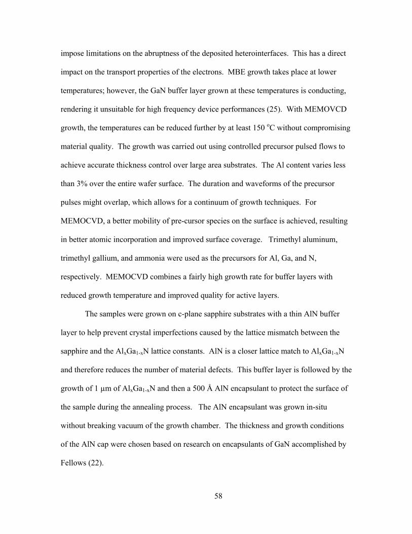
impose limitations on the abruptness of the deposited heterointerfaces. This has a direct
impact on the transport properties of the electrons. MBE growth takes place at lower
temperatures; however, the GaN buffer layer grown at these temperatures is conducting,
rendering it unsuitable for high frequency device performances (25). With MEMOVCD
growth, the temperatures can be reduced further by at least 150 oC without compromising
material quality. The growth was carried out using controlled precursor pulsed flows to
achieve accurate thickness control over large area substrates. The Al content varies less
than 3% over the entire wafer surface. The duration and waveforms of the precursor
pulses might overlap, which allows for a continuum of growth techniques. For
MEMOCVD, a better mobility of pre-cursor species on the surface is achieved, resulting
in better atomic incorporation and improved surface coverage. Trimethyl aluminum,
trimethyl gallium, and ammonia were used as the precursors for Al, Ga, and N,
respectively. MEMOCVD combines a fairly high growth rate for buffer layers with
reduced growth temperature and improved quality for active layers.
The samples were grown on c-plane sapphire substrates with a thin AlN buffer
layer to help prevent crystal imperfections caused by the lattice mismatch between the
sapphire and the AlxGa1-xN lattice constants. AlN is a closer lattice match to AlxGa1-xN
and therefore reduces the number of material defects. This buffer layer is followed by the
growth of 1 µm of AlxGa1-xN and then a 500 Å AlN encapsulant to protect the surface of
the sample during the annealing process. The AlN encapsulant was grown in-situ
without breaking vacuum of the growth chamber. The thickness and growth conditions
of the AlN cap were chosen based on research on encapsulants of GaN accomplished by
Fellows (22).
58

Samples from SET, Inc. are grown on double-side polished sapphire substrates
with only a small number scribed in the back surface, making it difficult to determine the
front and back side once the samples have been cut. Extra precautions must be made to
always mark the backside before cutting the wafer.
Cathodoluminescence Measurements
CL measurements were taken on the as-grown wafers to determine the Al
concentration. The most dominant peak in the spectrum should correspond to a band-to-
band transition which is equal in energy to the band gap of the material. The bandgap is
proportional to the Al mole fraction and thus, the luminescence peak of the material can
be used to determine the Al mole fraction of AlxGa1-xN. The mole fraction of the wafer is
determined through use of the fact that the energy band gap of AlxGa1-xN increases
almost linearly from that of GaN (3.4 eV) to that of AlN (6.2 eV), as shown in Equation
4.1, where the bowing parameter, b, was taken to be one. The bowing parameter has
been experimentally found to range from 0.78 to 1.14 depending on temperature (27).
)1()()1()()( xbxGaNExAlNxExE ggg −−−+= (4.1)
The measurements are taken at 7.4 K on three or more locations on the wafer to
check for the uniformity of the Al distribution. The CL spectra of the wafers as they
were received from SET, Inc are shown in Figure 4.1. The original CL spectra are taken
as a function of wavelength. The relation, )(/24.1)( meVE μλ= , is used to convert the
spectrum to photon energy. For all the samples, the spectra exhibited identical features
regardless of whether the measurements were taken from the edge or middle of the wafer;
however, the intensity decreased as the sampling moved from the middle to the edge.
The spectra shown in the figure are the results from sampling the middle of the wafers.
59

2.0 2.5 3.0 3.5 4.0 4.5 5.0
700600 500 400 300 200
CL
Inte
nsity
(arb
. uni
ts)
Energy (eV)
Al Mole Fraction 10% 20% 30% 40% 50%
3.7eV
3.9eV
4.1eV
4.4eV
4.6eV
Wavelength (nm)
Figure 4.1. CL Spectra taken at 7.4 K on the original wafers sent from SET, Inc. in order to investigate the quality of the material, as well as determine the Al mole fraction of each wafer.
60

The CL spectrum for the AlxGa1-xN wafers with 10, 20, and 30% Al concentration
exhibit a sharp band-to-band peak at a 3.7, 3.9, and 4.1 eV, respectively. The spectrum
of the Al0.4Ga0.6N wafer shows a broadened band-to-band peak at 4.4 eV with two
smaller peaks, seen as shoulders on the low energy side of the band-to-band peak. The
spectrum of the Al0.5Ga0.5N wafer has five peaks between 4.149 and 4.627 eV, with the
peak at 4.425 eV exhibiting the highest intensity. The energies of these peaks are 4.149,
4.333, 4.425, 4.528, and 4.627 eV. From the CL spectra, it appears that the high Al
concentration has degraded the crystal quality of the material. SET was contacted
regarding the wafer quality of the Al0.5Ga0.5N and responded by sending the transmission
spectrum they had taken for the wafer, shown in Figure 4.2, which clearly shows that the
band edge is about 271 nm, which would make the Al mole fraction of the wafer 51%.
With this evidence, the sample could not be refused and further processing continued,
assuming an Al mole fraction calculated from the transmission spectrum sent from SET,
Inc. The energy of the band-to-band transition and equation 4.1 were used to calculate
the Al mole fractions of the wafers and the results are summarized in Table 4.1.
Table 4.1. Values of interest for the determination of the Al concentration from CL spectra. The Al concentration of the Al0.5Ga0.5N wafer was determined from transmission measurements sent from SET, Inc.
Mole Fraction (%)
(Requested)
Peak Wavelength (nm)
(Observed)
B-B Energy Mole Fraction (eV) (%)
(Calculated) (Calculated)
10 335.0 3.701 14.27 20 316.8 3.914 24.50
30 301.6 4.111 33.20
40 280.4 4.422 45.74
50 273.8 4.627 51
61

200 300 400 500 600 700 800
0
20
40
60
80
100
bandedge@ (271nm)
Tr
ansm
issi
on (%
)
Wavelength (nm)
Al0.51Ga0.49N (1.8 μm)
Figure 4.2. The transmission spectrum sent from SET, Inc., for the Al0.5Ga0.5N wafer that shows a clear transition at 271nm indicating a good quality wafer that has 51% Al concentration.
Sample Cutting
The wafers are cut twice during the preparation process. First the wafers are
carefully cut into four quadrants in preparation of silicon implantation, as illustrated in
Figure 4.3(a). Each wafer quadrant is placed surface-side down on blue semiconductor
dicing tape to secure and protect it during the cutting process. The quadrants are cut with
a Loadpoint Limited Microace Series 3 saw, enabling precise adjustment of contact
62

pressure to ensure that the AlxGa1-xN is not damaged in the process. This processing step
was accomplished courtesy of Mr. Larry Callahan, of AFRL/SNDD.
The wafers from SET are polished on both the front and back sides and thus it is
virtually impossible to determine which side is the front, except for a small etching at the
bottom of the back of the sample. Prior to having these wafers cut, it is important to put a
mark on the backside of each quadrant to ensure the front and the back side can be
determined once the quadrants are removed from the tape.
The second cut, illustrated in Figure 4.3(b), comes after the ion implantation with
each of the wafer quadrants cut into 5 by 5 millimeter pieces. During the cutting process,
the small sample pieces can detach from the tape and become destroyed. Each quadrant
yields approximately 15 samples and several scrap pieces. The small scrap pieces were
used to determine the rate at which the AlN encapsulant is removed during a wet KOH
etch of the various wafers.
The samples are returned from the cutting process still on the cutting tape. The
samples should carefully be removed from the tape and scribed immediately before being
placed in the glassine envelope to ensure that the front and back sides can be
differentiated. A diamond tip pen is used to scribe the samples with a number
corresponding to their placement in the wafer quadrant and also with a unique symbol
that corresponds with their wafer quadrant. This ensures that each sample can be traced
back to its original placement in the whole wafer and that each sample’s markings are
unique.
63
Figure 4.3. A diagram to illustrate how the wafers are divided in preparation (a) for ion implantation and (b) for the annealing processes. The wafer shown in (a) is marked with the Si implantation dose for each quadrant. The wafer quadrant in (b) illustrates the naming system to track the location of the samples.
Ion Implantation
The introduction of silicon as a dopant in the AlxGa1-xN wafers was conducted
with ion implantation rather than diffusion or in-situ doping, due to advantages it offers
with regard to device manufacturing. Ion implantation enables doping profile
predictability, strict control of doping concentrations, and the ability to dope selective
areas of a material. These capabilities are critical for the design parameters of most
integrated circuits. Most semiconductor manufacturers use ion implantation almost
exclusively for doping in silicon ICs (1). There are also disadvantages associated with
64

this doping technique that must be a considered when ion implantation is chosen as the
doping method.
Ion implantation is a surface modification process that consists of bombarding the sample
surface with a high energy ion stream. The ions are produced in an accelerator and can
have typical energy ranges of 10-500 keV. Directed into a beam, they are uniformly
scanned across the wafer's surface until the desired dose is reached. A diagram of a
typical ion implantation setup can be seen in Figure 4.4. Common implanted doses range
from 1011 to 1016 ions per cm2. The profile of the implanted ions can be realized by
considering the stopping mechanisms of the implanted ions in the host material. The
depth of the ions into the material depends on the mass and energy of the ions as well as
the atomic mass and density of the host material.
Figure 4.4. A schematic diagram of a typical ion implantation experimental design (78).
65

The implanted ions enter the material and dissipate their energy through
interactions with the host atoms until they finally come to rest. Electronic and nuclear
interactions are the two main stopping forces that affect the movement of the dopant ions
(22). When the incoming ions collide in an inelastic manner with the host atoms' bound
electrons, the energy is transferred into heat or excitation of the host atoms. This is the
electronic stopping mechanism, and it is found to be proportional to the velocity of the
ions. The nuclear stopping mechanism occurs when the incident ions collide with host
atoms, causing equilibrium lattice position displacement of the host atoms. Displacing
one host atom can have a domino effect, displacing atoms throughout the material. The
electronic stopping dominates for ions with high energies, while the nuclear stopping is
the main force in low energy ions. This is due to the high energy ions moving too fast to
transfer enough energy to an incident atom during a collision to displace it. The
projected stopping range is therefore found to be proportional to the incident energy of
the implanted ions.
The first unified theory to determine the stopping and range of ions in matter
came about in 1963 and is named the LSS-theory after the initiating scientists Lindhard,
Scharff, and Schiott (78). The theory, in the beginning, made some broad
approximations in the statistical model representing the atom to atom collisions as a
Gaussian distribution centered around the average projected range, Rp, and having a
standard deviation of ΔRp. In the theory, the penetrating ion beam is considered to scan
the target material uniformly to limit the variation to the projected direction only, i.e. to
reduce the lateral straggle. The theory was valid for the entire atomic spectrum and
found to be accurate to within a factor of two for single element amorphous targets (28).
66

The theory was improved in the next twenty years by replacing some of the initial
approximations with new advances in theory, and the advent of computers introduced
numerical techniques which also increased accuracy. As of 2003, the accuracy of
determining the stopping ranges of ions in matter was within 5% margin of error overall,
with a 6% margin of error for heavy ions, and a less than 2% margin of error for high
velocity light ions (79).
The theory considers the mass and energy of the ions as well as the atomic weight
and density of the host material to determine the parameters that are used to define the
shape of the Gaussian profile, the projected range, and the projected straggle of the ions.
The volume concentration of the ions is given in equation 4.2 with φ being the implanted
ion dose (22).
⎥⎥
⎦
⎤
⎢⎢
⎣
⎡
⎟⎟
⎠
⎞
⎜⎜
⎝
⎛
Δ
−−
Δ=
2
2exp
2)(
p
p
p R
Rx
RxN
πϕ . (4.2)
The peak concentration will occur at a distance Rp beneath the surface. Considering
equation 4.2, the peak concentration is easily determined and given by.
pp R
RNΔ
=πϕ
2)( . (4.3)
The Gaussian profile from the LSS theory is predicted for an amorphous target but has
been found to be a good first order approximation for crystalline solids as well. When
the ion implantation is performed, the target is tilted (normally 7º off axis) in relation to
the incident ion beam, making the incoming beam's target appear more amorphous.
Having the ion beam enter the material off-axis ensures that the ions do not travel in
67

between planes in the crystal and move unobstructed from collisions. The tilt, in effect,
reduces the effects of channeling.
The calculations to determine the ion depth profile were accomplished using a
prewritten commercial code called TRIM which is short for TRansport of Ions in Matter
(28). TRIM is a comprehensive program that considers all of the kinetic mechanisms
associated with the loss of energy of the ion such as sputtering, ionization, phonon
production, and target damage. An example of the predicted depth profiles of silicon and
gold ions into a GaN sample with a 500 Å AlN encapsulant can be seen in Figure 4.5 for
an ion dose of 1x1015 cm-2 at various ion energies.
Figure 4.5. The predicted TRIM depth profiles for Si ions at various energies and Au at 300 keV in to GaN with a 500 Å AlN encapsulant to illustrate the effects that the ion’s energy and mass have on the shape of the depth profile.
68

The program can be used for complex targets with up to eight unique layers and
follows the atom trajectories in the target in-depth. Ideal implantation would result in
the peak concentration lying directly beneath the surface of the AlxGa1-xN material,
requiring the Si ions to travel through the 500Å AlN encapsulant. The ion implantation
conditions such as energy and dose were determined in advance using TRIM code. Ion
implantation services are contracted out through CORE Systems (Sunnydale, CA). The
implantation was accomplished with the AlxGa1-xN wafers at room temperature, tilted at a
7º to minimize channeling. The implanted silicon ions had an energy of 200 keV and
doses of 1x10¹⁴, 5x10¹⁴, and 1x1015 cm-3.
Annealing
The discussion in this section follows the development and presentation found in
Fellows’ dissertation (22). The implanted ions enter the host lattice and slowly dissipate
their energy through electronic and nuclear stopping mechanisms, leaving an assortment
of defects in their wake. As mentioned previously, nuclear stopping involves an incident
ion colliding with the host atom and displacing it from its equilibrium lattice position.
The displaced host atom will then collide with other atoms/ions instituting a cascading
effect that leaves the crystal lattice in a disordered state littered with simple and complex
defects that will degrade the electrical and optical properties of the material. The
implanted ions will most likely come to rest in an interstitial position within the crystal
lattice. To repair the disordered state of the crystal and shift the implanted ions to
electrically active lattice positions, the sample must endure a high temperature anneal. It
is a general rule that the annealing temperature required to fully remove the defects is ⅔
69
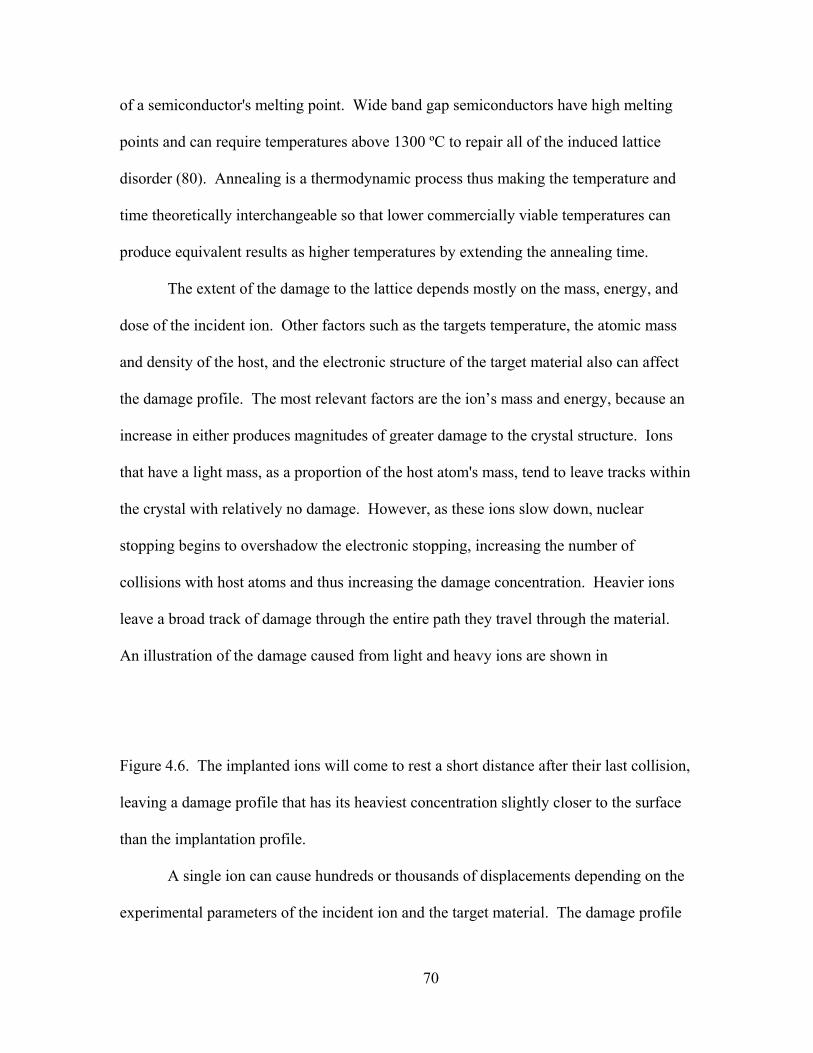
of a semiconductor's melting point. Wide band gap semiconductors have high melting
points and can require temperatures above 1300 ºC to repair all of the induced lattice
disorder (80). Annealing is a thermodynamic process thus making the temperature and
time theoretically interchangeable so that lower commercially viable temperatures can
produce equivalent results as higher temperatures by extending the annealing time.
The extent of the damage to the lattice depends mostly on the mass, energy, and
dose of the incident ion. Other factors such as the targets temperature, the atomic mass
and density of the host, and the electronic structure of the target material also can affect
the damage profile. The most relevant factors are the ion’s mass and energy, because an
increase in either produces magnitudes of greater damage to the crystal structure. Ions
that have a light mass, as a proportion of the host atom's mass, tend to leave tracks within
the crystal with relatively no damage. However, as these ions slow down, nuclear
stopping begins to overshadow the electronic stopping, increasing the number of
collisions with host atoms and thus increasing the damage concentration. Heavier ions
leave a broad track of damage through the entire path they travel through the material.
An illustration of the damage caused from light and heavy ions are shown in
Figure 4.6. The implanted ions will come to rest a short distance after their last collision,
leaving a damage profile that has its heaviest concentration slightly closer to the surface
than the implantation profile.
A single ion can cause hundreds or thousands of displacements depending on the
experimental parameters of the incident ion and the target material. The damage profile
70
may be so large that the concentration of displacements is on the order of the atomic
density of the crystal lattice; in this case the crystal structure is completely destroyed
leaving an amorphous structure. Damage on this great of a level suppresses all electrical
and optical properties of the material and may not be able to be repaired through high
temperature annealing.
Ionic materials, which comprise the majority of semiconductors, are more
resistant than most substances to becoming amorphous. These materials exhibit natural
dynamic annealing in which they repair structural damage during the implantation
process. Dynamic annealing is a beneficial property because it quenches the formation of
stable lattice disorders that resist repair (29). Raising the substrate temperature during the
implantation can enhance the effects of dynamic annealing. The added heat increases the
lattice vibrations and aids in moving the atoms and ions into equilibrium lattice sites.
71

Figure 4.6. An illustration of the lattice disorder that results from the ion implantation of a light and heavy ion, respectively (22, 37).
The structural disorder of ion implanted AlxGa1-xN, with x from 0 to 0.6, was
studied by Kucheyev and Williams, et al. (30). They observed that increasing Al content
strongly enhanced the effects of dynamic annealing in AlxGa1-xN. They reported the
amorphization behavior to be different from that of GaN, in that AlxGa1-xN did not
display any preferential surface disordering. Rather, the AlxGa1-xN exhibited “a rapid
transition from the saturation regime to the nucleation-limit amorphization in the crystal
bulk” when implanted above the critical dose (Au, 300 keV, 3x1015 cm-2) and that this
effect is relatively independent of the Al concentration of the sample (30). The Au
implantation resulted in lattice disorder mainly in the bulk region of the AlxGa1-xN where
the nuclear defect profile has a maximum with the given implant conditions and a dose
up to 1x1015 cm-2. The bulk region exhibits saturation while the damage level at the near
surface region grows up to the saturation level. The surface of GaN shows a strong
preferential site for amorphization resulting in the crystal becoming amorphous layer by
72

layer beginning at the surface. AlxGa1-xN, on the other hand, becomes amorphous
spontaneously in the bulk region and then proceeds to the surface layers. XTEM (cross-
sectional transmission electron microscopy) measurements show the existence of buried
amorphous layers in the AlxGa1-xN epilayers, which increase with Al content, when
implanted above the critical dose. XTEM measurements also revealed similar extended
defects and defect clusters as those found in GaN.
The incident ions collide with the host atoms resulting in a multitude of defect
complexes involving vacancies, antisites, and interstitials. When any one of these defects
occurs, they produce unpaired valance electrons that cause the defect to become ionized.
An aluminum vacancy, VAl, leaves four nitrogen atoms three electrons short of forming
complete valance shells, making the defect a triple acceptor. On the other hand, a
nitrogen vacancy, VN, creates a center with four Al or Ga atoms, with each atom having
three available valance electrons. Two of these atoms will bond, forming an electron-
electron pair, thus leaving this defect a single donor. An antisite in group III-V
compound semiconductors, when the anion host atom resides on the cation lattice site or
vice versa, can act as a double donor or a double acceptor. For example, a gallium or
aluminum antisite, GaN or AlN, is two electrons short of completing all the necessary
bonds of the N atom, thus producing a double acceptor. While a nitrogen antisite, NGa or
NAl, will have two extra electrons after completing all the bonds and is therefore a double
donor.
The ionic nature of the defects will cause them to combine and form defect
complexes with the defects mentioned above and those involving the Si-implanted ions.
In III-V semiconductors, it is energetically favorable for a group IV dopant to occupy
73

either the cation or anion lattice position acting as a single donor or a single acceptor. A
silicon ion occupying a gallium lattice site, SiGa, is a single donor. This defect will be
attracted through Coulomb forces to a triple acceptor VAl. These two defects combine to
form a double acceptor complex. The host atoms and the implanted ions strive to achieve
a lattice configuration with the most favorable energy configurations, which represents
the primary determinate as to which types of defect complexes form.
These defects create deep energy levels within the band gap that act as non-
radiative recombination centers for the free carriers, essentially trapping them and
preventing their participation in the conduction. These traps compensate the shallow
donors and acceptors that are intentionally introduced into the material to enhance the
conduction properties. The random distribution of the atoms that results from the ion
implantation increases the number of scattering centers which can reduce free carrier
mobility. The material defects are not all a result of the ion implantation; some defects
are inherent to the material growth techniques and result from the lack of a perfectly
lattice-matched substrate on which to grow the AlxGa1-xN epilayers. Evaluation of the as-
grown material is essential for the determination of the as-grown defect level to provide a
baseline for evaluating the degree of crystal damage recovery of the implanted samples.
Defects, such as disassociated host atom, can also result from the high temperature anneal
requirement.
The high temperature anneal is designed to give the host atoms and implanted
ions enough thermal energy to form the ordered lattice structure that the material initially
obtained. The goal is to repair the defects that were created and to shift the implanted
ions to electrically active lattice positions. It is more difficult to recreate lattice order in
74

compound semiconductors compared to elemental semiconductors due to the difficulty
involved in getting the atoms to occupy the correct anion or cation lattice sites. The
stoichiometry of the crystal must be maintained, which is difficult due to the mass
difference of the host atoms which allow lighter atoms to travel further once displaced
from their equilibrium positions. At high temperatures, the nitrogen atoms become
volatile and disassociation of these atoms becomes a setback.
There are three common techniques used to prevent disassociation of the
material's host atoms: inert gas overpressure in the annealing chamber, face-to-face
proximity annealing configuration, and a protective encapsulant deposited on the surface
of the samples. With inert gas overpressure, an overpressure of the element with the
lowest vapor temperature, normally the group V atoms, applies a slight pressure to the
sample surface reducing the group V disassociation. In the face-to-face configuration,
samples are placed on top of each other with the implanted surfaces in direct contact.
This precautionary method forces the disassociated N atoms into the surface of the other
sample. This configuration also protects the sample surface from pitting, cracking, and
peeling from the high anneal temperatures. The most effective way to prevent group V
evaporation is to cover the surface of the sample with an encapsulant that can be grown
on epitaxially or deposited after growth. An in-situ grown encapsulant should be
deposited uniformly, so that it does not affect the depth profile of the implanted ions.
The encapsulant material should have a thermal expansion coeffient close to that of the
sample material as to not induce strain related defects during the annealing process. Thin
encapsulants have been shown to handle lattice mismatches better and also resist pealing
and cracking better than thicker caps (22). Common encapsulants for nitride materials
75

are AlN and SiC due to their high thermal integrity and their ease of removal from the
surface after the anneal.
A conventional furnace anneal, CFA, is the most common type of anneal used for
post ion implantation treatments. They are characterized by their long rise times as well
as long dwell times. CFA’s are capable of reaching higher temperatures (≤ 1200 ºC) and
maintaining them reliably for extended periods. Defect and defect complexes have
different thermal activation energies and therefore restore themselves at different
temperatures. The CFA anneal allows the sample to experience each temperature range
for a short duration, thus allowing different types of defects to recover. Another type of
annealing is a rapid thermal anneal, RTA, which is defined by its ability to quickly ramp
the temperature to the desired set point using halogen lamps. Rapid thermal anneals have
very short dwell times, typically less than a minute. Short dwell times limit the amount
of dopant diffusion that takes place at high temperatures and prohibits the widening of the
depth profile. RTA’s are common on production lines due to their quickness and
reliability. Annealing can also be accomplished using a high powered ion beam
annealing to melt the surface layer of the material and allow it to rapidly solidify. High
powered ion beam annealing is not often applied due to atom disassociation occurrences.
All samples for this study were annealed in an Oxy-Gon Industries furnace
uniquely designed to shorten the rise and fall times of the sample. The furnace is
equipped with separate chambers for sample access and heating, which allows samples to
be inserted and removed via a preheated access chamber without altering the heating
chamber's temperature. The quick temperature change from room temperature to
temperatures higher than 1150 ºC allows the sample to spend more time at the actual
76

annealing set point temperature. The sample's temperature is rapidly decreased from the
annealing temperature to room temperature once the annealing time has expired. The
Oxy-Gon furnace has the capability to be heated to 2500 oC, however, most commercial
furnaces do not exceed 1200 ºC. The AlxGa1-xN samples in this study were annealed
from 1150 to 1350 oC from 20 to 40 minutes. Specific operating instructions for the
furnace can be found in appendix A.
In preparation for the anneal, this study's samples were placed face-to-face and
held together by wrapping tantalum (Ta) wire around them at the center of the sample's
width and depth planes, and intertwined and secured at top center, similar to the way
packages are often wrapped with string. The sample “packets” are placed on the graphite
hearth in the access chamber and then covered with a two inch sapphire wafer to ensure
that the samples remain on the hearth during the transport into the heating chamber. The
environment inside the sample access and heating chambers is placed under a vacuum of
10-6 Torr. In order to rid the chambers of oxygen and other contaminates the chambers
were flushed several times before being filled with high purity nitrogen gas. The heating
chamber is then warmed to the desired temperature. Once the anneal temperature has
stabilized, the samples are moved into the heating chamber. The official start time for the
anneal begins once the samples are in the heating chamber. Sample temperature profiles
of set point and furnace stabilization rates are illustrated in Figure 4.7.
77

-25 0 25 50 75 100 125 150 175 200 225 250 275 300 325
0
200
400
600
800
1000
1200
1400
Tem
pera
ture
( o C
)
Time (sec.)
Heat Zone Sample Temp.
Figure 4.7. The temperature profile for the Oxy-Gon furnace used for the high temperature post implantation anneal. It takes about 75 seconds for the heat zones temperature to stabilize after the samples are introduced into the chamber and also to bring the samples up to temperature.
After the heating phase, the samples are quickly lowered from the heating
chamber and cooled to room temperature in a flowing N2 ambient to prevent surface
oxidation. The Ta wrapping wire survives the anneal intact, but becomes brittle enough
to easily break off. The samples are taken to the clean room before being separated and
inspected for damage.
78

AlN Encapsulant Removal
After the high temperature anneal, the AlN encapsulant, which must be removed
to expose the AlxGa1-xN surface, was eliminated by soaking the samples in a 0.5 molar
solution of potassium hydroxide (KOH) and de-ionized (DI) water. The etch rate of the
AlN in the KOH solution varied as a function of the Al mole fraction of the sample
material. The etch rate rapidly reduced as the Al mole fraction of the material increased
from 10 to 50%. A systematic study of the AlN etch rate as a function of Al mole
fraction in AlxGa1-xN was carefully conducted to determine the time for each type of
sample in the solution. The etch time varied from 5 minutes for GaN to 20 minutes for
Al0.5Ga0.5N. Figure 4.8 illustrates the etch rate of the AlN as a function of Al
concentration.
After the removal of the AlN cap, the samples were rinsed thoroughly with DI
water before being placed in an acidic bath of 3:1 HNO3 and HCl (known as aqua regia)
for two minutes to clean the sample surface of oxidation. Following the acid bath, the
samples were rinsed again with DI water and blown dry with N2 in preparation for the
deposition of metal ohmic contact stacks.
Ohmic Contacts
The electrical properties of the Si-implanted AlxGa1-xN could not be obtained
without the deposition of an ohmic contact. Once the samples were cleaned, they were
placed in a van der Pauw shadow mask which only permits metal to be deposited in small
points onto the four corners of the sample. The number of samples that could be
processed at one time was restricted by the van der Pauw mask's ten sample limit and the
evaporator's two mask capacity.
79

The metal stacks of Ti/Al/Ti/Au, with thicknesses of 120/40/80/55 nm, were
deposited in the clean room using a Denton Evaporator (64). The evaporation was
performed under vacuum of 10-7 torr, utilizing high purity metal sources. As-deposited
contacts exhibit rectifying behavior, so they were heated for a short period to instill
ohmic properties. The contacts were rapidly thermally annealed in a clean room furnace
called an RTP (rapid thermal process), where they were heated to 900 oC for 30 seconds
in flowing nitrogen ambient. The resulting samples with highly ohmic contacts then
underwent electrical, and later, optical testing.
80

0 10 20 30 40 50
2
4
6
8
10
Et
ch ra
te (n
m/m
in.)
Al Concentration (%)
Figure 4.8. The etch rate of AlN on AlxGa1-xN as a function of Al mole fraction when placed in a 5 M solution of KOH and DI water. The etch rate decreases rapidly as the Al concentration of the material increases.
81

82
V. Results
The results presented here provide a catalog of the electrical and optical properties
of silicon implanted MEMOCVD grown AlxGa1-xN as a function of aluminum
concentration, implantation dose, anneal temperature and anneal time. This research will
benefit device engineers by improving the performance of AlxGa1-xN based devices that
require ion implantation. The objective of this comprehensive study is to optimize the
silicon ion implantation and anneal conditions for AlxGa1-xN as a function of the Al mole
fraction to create a more suitable material for optical and electronic device purposes.
Ion implantation is a commonly utilized technique for the fabrication of
semiconductor devices that are based on Si and GaAs materials. It is a crucial processing
step that lends for precise controlled doping of nitride-based devices. Ion implantation of
various ions, doses, and energies is used for device isolation, creating highly conductive
n-type regions for improving access resistance and the fabrication of the channel layer in
transistors. The fabrication of many AlxGa1-xN /GaN devices already involve ion
implantation and more often the focus has begun to shift to activation of an implanted
species into AlxGa1-xN rather than GaN. The last decade has seen a drastic increase in the
understanding of the defect structures caused by ion implantation into GaN and how their
stability against annealing can affect the activation of the implanted species. At the
present time, little research has been conducted into the properties of ion implanted
AlxGa1-xN. The knowledge of GaN will undoubtedly aid in the investigation of AlxGa1-
xN; however, how these properties change as a function of Al mole fraction has yet to be
determined.

83
Successful application of ion implantation depends on understanding the
production and annealing of radiation induced damage in the material. Ion implantation
parameters that are responsible for the lattice damage are beam flux, implantation
temperature, and the ion’s mass and energy. Kucheyev et al. investigated damage
profiles obtained from Rutherford backscattering spectrometry (RBS) and cross-sectional
transmission electron microscopy (XTEM) measurements and found that the damage
accumulation in GaN under bombardment occurs at the surface and in the bulk of the
material (31). They found that the parameter that has the most profound effect on the
amount of damage accumulation that will occur in GaN is the beam flux or implantation
dose. Increasing the implantation dose above a critical dose will cause the surface
damage and bulk damage to grow causing them to meet resulting in thick layer
amorphization. The ion’s mass also exhibited a great impact on the level of implantation
produced lattice disorder. Heavy ion bombardment could cause amorphization of the
material that would begin at the surface and proceed layer by layer into the bulk of the
material. Kucheyev et al. observed that the ion implantation temperature was found to
reduce damage accumulation as the temperature was raised from room temperature to
600 K, however lower and higher implantation temperatures had negative effects on the
damage profile. According to Kucheyev’s experiment, the ion’s energy did not exhibit as
great an influence on the damage profile when compared to the other parameters. Both
Kucheyev and Zopler report that the effects of dynamic annealing, which are strong in
GaN, help to suppress the formation of stable lattice defects during the ion implantation
process and as a result the most common defects found in bombarded GaN are planar
defects in the form of interstitials (31, 32). Most literature reports that an anneal
temperature greater than 1300 ºC is required for optimal activation of an implanted

84
species in GaN and an even higher temperature is theorized for AlxGa1-xN materials (29-
32).
It is reported by Kucheyev et al. that AlxGa1-xN experiences a stronger dynamic
annealing effect than GaN, and that increasing the Al content acts to enhance this feature
due to the larger energy of the Al-N bond as compared to the Ga-N bond (32). Kucheyev
studied AlxGa1-xN (x = 0.05-0.60) and observed that AlxGa1-xN, unlike GaN, did not
exhibit disordering of the lattice at the surface (29, 31). Instead, the damage
accumulation in AlxGa1-xN occurred in the bulk of the material. Implantation above a
critical dose (>1020 cm-2) resulted in rapid amorphization of the bulk material which
spread layer by layer to the surface. Raising the concentration of Al in the material
resulted in an elevated critical dose which could be due to the increased effects of
dynamic annealing causing a decrease in implantation produced disorder.
For intentional n-type doping of AlxGa1-xN, silicon is the most widely used dopant
due to its predicted shallow donor level over the complete spectrum of Al compositions.
The silicon ionization energy is theorized to increase with increasing Al content from 20
meV for GaN to 90 meV for AlN (33). Experimentally, there have been few reports on
n-type conductivity achieved through ion implantation in AlxGa1-xN with high Al
concentrations. The majority of the research thus far has focused on ion implanted
AlxGa1-xN with Al mole fractions less than 30% due to difficulty in growing good quality
AlxGa1-xN epilayers with higher Al mole fractions. Research of AlxGa1-xN properties is
minimal and at this time there exist no in-depth data on the fundamental properties of ion
implanted AlxGa1-xN for n-type conductivity. This study provides a systematic
investigation into the electrical and optical properties of silicon implanted AlxGa1-xN as a
function of Al concentration, implant dose, anneal temperature, and anneal time to
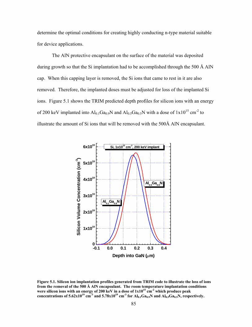
determine the optimal conditions for creating highly conducting n-type material suitable
for device applications.
The AlN protective encapsulant on the surface of the material was deposited
during growth so that the Si implantation had to be accomplished through the 500 Å AlN
cap. When this capping layer is removed, the Si ions that came to rest in it are also
removed. Therefore, the implanted doses must be adjusted for loss of the implanted Si
ions. Figure 5.1 shows the TRIM predicted depth profiles for silicon ions with an energy
of 200 keV implanted into Al0.1Ga0.9N and Al0.5Ga0.5N with a dose of 1x1015 cm-2 to
illustrate the amount of Si ions that will be removed with the 500Å AlN encapsulant.
-0.1 0.0 0.1 0.2 0.3 0.40
1x10¹⁹
2x10¹⁹
3x10¹⁹
4x10¹⁹
5x10¹⁹
6x10¹⁹
Al0.5Ga0.5N
Si, 1x1015 cm-2, 200 keV implant
Silic
on V
olum
e C
once
ntra
tion
(cm
-3)
Depth into GaN (μm)
Al0.1Ga0.9N
Figure 5.1. Silicon ion implantation profiles generated from TRIM code to illustrate the loss of ions from the removal of the 500 Å AlN encapsulant. The room temperature implantation conditions were silicon ions with an energy of 200 keV in a dose of 1x1015 cm-2 which produce peak concentrations of 5.62x1019 cm-3 and 5.78x1019 cm-3 for Al0.1Ga0.9N and Al0.5Ga0.5N, respectively.
85

The AlxGa1-xN sample surface begins at 0 µm on the graph. As can be seen from the
figure, the quantity of removed Si ions decreases as the Al mole fraction in the sample is
increased. This is due to the decreasing density of the material as the Al mole fraction is
increased allowing for the implanted ions to come to rest further into the material with
less residing near the surface. Simple integration of the curve shows that 1.9% of the
implanted ions are removed for the Al0.1Ga0.9N samples and 1.6%, 1.3%, 1%, and 0.7%
of the ions are removed for the samples with Al with mole fractions of 0.2, 0.3, 0.4, and
0.5, respectively. The implanted dose will be corrected for this removal of ions and an
effective dose will be used for calculation of the silicon activation efficiency and the
silicon ionization energy.
As discussed by Fellows, the silicon electrical activation efficiency represents that
the percentage of the implanted Si ions that contribute to the electrons in the conduction
band (22). While the silicon ionization energy represents the energy required to ionize a
silicon ion in a non-degenerately doped semiconductor and can be extracted from the
relationship exp(-Ed/kBT). To calculate the activation efficiency the room temperature
carrier concentration, , is divided by the effective implanted silicon dose,sn effϕ . The
silicon electrical activation efficiency therefore only considers the percent of
substitutional donors in the material. The donor activation, given in equation 5.1,
incorporates the ionization energy and thus corresponds to the percent of ionized donors.
In equation 5.1, Ed is the donor ionization energy, kB is the Boltzman constant, and T is
the temperature (22).
TkEeff
sBde
n/−=
ϕη (5.1)
86

87
Silicon Implanted Al0.1Ga0.9N
The studies of ion implanted AlxGa1-xN are minimal with most of the work
focusing on AlxGa1-xN with lower Al concentrations. Y. Irokawa et al. investigated the
electrical activation characteristics Al0.13Ga0.87N implanted with silicon ions that had
multiple energies to achieve a uniform concentration at 4 µm into the material (34). They
achieved greater than 90% electrical activation for the samples implanted with a silicon
dose of with 5.2x10¹⁴ and 1x1015 cm-2 after annealing at 1375 ºC for 5 minutes in a
nitrogen environment. The sample implanted with 1x1014 cm-2 silicon ions had a
considerably lower electrical activation of 55% under the same annealing conditions.
Zopler et al. observed an electrical activation of only 34% after implanting Al0.15Ga0.85N
with silicon ions that had an energy of 100 keV and a high dose of 5x1015 cm-2 after
annealing under high nitrogen pressures (32). Ryu et al. reported activation efficiencies
of 45% and 76% for Al0.14Ga0.86N implanted with silicon ions that had an energy of 200
keV at doses of 5x10¹³ and 1x1014 cm-2, respectively, and subsequently annealed at 1250
ºC for 20 minutes in flowing nitrogen (35). Polyakov et al. achieved only 10% activation
after annealing at 1140 ºC for Al0.12Ga0.88N implanted with 5x1014 cm-2 silicon ions (36).
Exhibiting such low activation energies at the lower temperature anneals reveals a shift in
behavior from GaN which exhibited silicon activation efficiencies above 50% even in
cases where structural damage recovery was incomplete (34). This trend indicates that
higher anneal temperatures may be required for significant activation in AlxGa1-xN to take
place. This section details the findings of silicon implanted Al0.1Ga0.9N as a function of
anneal temperature and time through Hall Effect and cathodoluminescence
measurements.

88
Room Temperature Hall Effect Measurements
The MEMOCVD grown Al0.1Ga0.9N was capped with 500Å of AlN and then
implanted at room temperature with silicon ions that had an energy of 200 keV to
produce the desired dose. The Si doses were 1x10¹⁴, 5x10¹⁴, and 1x1015 cm-2 which after
taking into account the 500Å AlN cap the effective doses are 9.8x10¹³, 4.9x10¹⁴, and
9.8x1014 cm-2, respectively. The samples were annealed from 1100 to 1250 ºC for 20 to
40 minutes in a flowing nitrogen environment. All the samples had excellent surface
morphology following the anneal at 1250 ºC, increasing the anneal temperature to 1300
ºC however, caused significant damage to the surface for these samples. Room
temperature Hall Effect measurements were conducted to determine sheet carrier
concentrations for the samples annealed for 20 minutes and the results are shown in
Figure 5.Figure 5.2. The unimplanted samples both as-grown and annealed were highly
resistive making it impossible to collect any meaningful data. However, there was one
exception. The room temperature carrier concentration of the unimplanted sample that
had been annealed at 1250 ºC for 20 minutes was 6.5x1012 cm-2, and this value was
subtracted from the implanted sample’s measurements as the background carrier
concentration. The fact that an annealed unimplanted sample had a measurable carrier
concentration, while the as-grown material did not, could indicate that the as-grown
defects were compensating residual shallow donors that were repaired during the
annealing process, thus allowing the shallow donors to contribute to the conduction.
The sheet carrier concentrations for each implanted silicon dose respond
differently to an increase in the anneal temperature. The carrier concentration for the
Al0.1Ga0.9N implanted with a silicon dose of 1x1014 cm-2, shown as a solid square,
increases almost linearly as the anneal temperature is increased from 1100 to 1200 ºC, but

1100 1150 1200 1250
1100 1150 1200 1250
1E13
1E14
1E15
1E13
1E14
1E15
Shee
t Car
rier C
once
ntra
tion
(cm
-2)
Anneal Temperature (oC)
Al0.1Ga0.9N:Si Unimplanted 1x1014 cm-2
5x1014 cm-2
1x1015 cm-2
tA = 20 minutes
Figure 5.2. Room temperature sheet carrier concentrations for Al0.1Ga0.9N implanted with Si at 200 keV at room temperature with doses of 1x10¹⁴, 5x10¹⁴, and 1x1015 cm-2 and subsequently annealed from 1100 to 1250 ºC for 20 minutes in flowing nitrogen.
89

90
the increase in carrier concentration is much less between the 1200 and 1250 ºC anneal.
These samples experienced a maximum carrier concentration of 6.69x1013 cm-2, after
being annealed at 1250 ºC for 20 minutes in nitrogen ambient. The rapid increase in
carrier concentration was only witnessed in the Al0.1Ga0.9N implanted with the lowest
silicon dose. The Al0.1Ga0.9N samples implanted with a silicon dose of 5x1014 cm-2,
shown by the solid circle, exhibit their most noticeable increase in carrier concentration
between the 1100 and 1150 ºC anneals although concentrations at that dose were
relatively weak. The carrier concentration for these samples continues to increases
through the 1200 ºC anneal, reaching a maximum of 3.66x1014 cm-2 at this anneal
temperature. Further increasing the anneal temperature to 1250 ºC causes the carrier
concentration to decrease back to the value obtained for the sample that was annealed at
1150 ºC. The Al0.1Ga0.9N samples implanted with the highest Si dose of 1x1015 cm-2,
shown by the solid triangle, have very high carrier concentration even after being
annealed at 1100 ºC and 1150 ºC of roughly the same value, with the sample annealed at
1150 ºC being only slightly higher at 8.92x1014 cm-2. Increasing the anneal temperature
for the samples implanted with this dose to 1200 ºC results in a decrease in the carrier
concentration and even more so when the anneal temperature is raised to 1250 ºC. The
samples implanted with the highest silicon dose show a decrease in the carrier
concentration as the temperature is elevated above 1150 ºC while the samples implanted
with the middle dose of 5x1014 cm-2 does not begin to decrease until after the anneal
temperature is above 1200 ºC. The carrier concentration for the samples implanted with
the lowest silicon dose increases throughout the given temperature range.
The silicon electrical activations, are shown in Figure 5.3, of these samples are
closely related to the carrier concentrations and thus follow the same trends with the

1100 1150 1200 1250
1100 1150 1200 1250
0
10
20
30
40
50
60
70
80
90
100
0
10
20
30
40
50
60
70
80
90
100
tA = 20 minutes
Silic
on E
lect
rical
Act
ivat
ion
Effic
ienc
y (%
)
Anneal Temperature (oC)
Al0.1Ga0.9N:Si
1x1014 cm-2
5x1014 cm-2
1x1015 cm-2
Figure 5.3. Electrical activation efficiency for silicon implanted Al0.1Ga0.9N calculated from the room temperature Hall measurements doses of 1x10¹⁴, 5x10¹⁴, and 1x1015 cm-2 and annealed from 1100 to 1250 ºC for 20 minutes.
91

92
anneal temperature as mentioned above. The electrical activation efficiency was
calculated using the effective dose, and the room temperature carrier concentration.
Higher implanted doses resulted in higher silicon activation efficiencies for anneal
temperatures up to 1250 ºC, except in the case of the sample implanted with 1x1014 cm-2
and annealed at 1250 ºC which exhibits a slightly higher activation than the sample
implanted with 5x1014 cm-2 and annealed at 1250 ºC. The silicon electrical activation for
the samples implanted with 1x1014 cm-2 silicon ions exhibits the most improvement over
the given temperature range, increasing from 22% to 68% after being annealed for 20
minutes at 1100 ºC and 1250 ºC, respectively. The samples implanted with a dose of
5x1014 cm-2 silicon ions have a significant activation efficiency of 51% after the 1100 ºC,
20 minute anneal, and steadily increases to a maximum of 75% following the 1200 ºC
anneal before dropping off at the 1250 ºC anneal to the same activation as the 1150 ºC
anneal. The decrease in activation efficiency could be due to out diffusion of silicon or
compensating acceptor-like defects that were created during the higher temperature
anneals. The samples implanted with the highest silicon dose, 1x1015 cm-2, exhibit the
highest activation efficiencies of all the implanted doses reaching 88% and 91%
following the lower temperature anneals of 1100 ºC and 1150 ºC, respectively. The
activation for the high dose implanted samples then declines to 80% and 76% for the
higher temperature anneals of 1200 ºC and 1250 ºC, respectively. The samples implanted
with the higher silicon dose experience more damage from the ion bombardment which
would create more lattice damage. That, paired with the high temperature anneal which
can also create defects in the material, may allow for the implanted silicon ions to be
more inclined to occupy nitrogen lattice sites. If this were to occur, the silicon ions that
occupy nitrogen sites would compensate the electrons donated to the conduction by the

93
silicon ions that occupy gallium or aluminum sites and the activation efficiency would
decrease. All three doses display their peak electrical activation at different temperatures,
with optimal anneal temperatures decreasing in inverse relation to increased implantation
doses.
The higher implanted silicon doses were more readily activated than the lower
implanted silicon doses into Al0.1Ga0.9N. To better illustrate the improvement in
activation with dose, the sheet carrier concentration is plotted as a function of the
implanted silicon dose in Figure 5.4. It is clear from the figure that the samples
implanted with the highest silicon dose achieve higher electrical activation efficiencies at
lower anneal temperatures than the samples implanted with the lower silicon doses. The
Al0.1Ga0.9N implanted with the lower silicon doses, even at the highest annealing
temperatures, do not respond as well as the high dose implantation at its worst activation.
Implanted silicon in GaN was found to behave similarly, though GaN did not exhibit a
decrease in the activation efficiency as the anneal temperature was increased even for
implanted silicon doses as high as 5x1015 cm-2 and anneal temperatures as high as
1350°C (22).
The electrical activations are comparable to other previous findings. The low
silicon dose implantation, 1x1014 cm-2, exhibits an electrical activation of 68% following
a 1250 ºC anneal for 20 minutes in flowing nitrogen. Ryu et al. reported a slightly
higher activation of 76% for Si implanted MBE grown AlxGa1-xN under the same
implantation and anneal conditions (35). The silicon implantation dose of 5x1014 cm-2
reached a maximum electrical activation of 75% after being annealed at 1200 ºC for 20
minutes. Irokawa et al. reported a higher activation of 90% for a sample implanted with a
similar dose but the annealing temperature was considerably higher at 1375 ºC with an

1E14 1E15
1E14
1E15Sh
eet c
arrie
r Con
cnet
ratio
n (c
m-2)
Actual Implanted Si Dose (cm-2)
Al0.1Ga0.9N:Si 1100oC/20min. 1150oC/20min. 1200oC/20min. 1250oC/20min.
100% Activation
Figure 5.4. The room temperature sheet carrier concentrations versus the actual implantation dose for Al0.1Ga0.9N implanted with 200 keV silicon at room temperature with doses of 1x10¹⁴, 5x10¹⁴, and 1x1015 cm-2 and annealed from 1100 ºC to 1250 ºC for 20 minutes in a nitrogen ambient.
94

95
anneal time of 5 minutes (34). Irokawa et al. also reported 90% activation for a sample
implanted with a silicon dose of 1x1015 cm-2 under the same anneal conditions. In this
study, however, 91% activation was achieved for this dose at a much lower annealing
temperature of 1150 ºC, with an extended time, 20 minutes.
The data show that for the low dose Si-implantation into Al0.1Ga0.9N, the optimal
anneal temperature may be higher than 1250 ºC while the optimal anneal temperature for
the samples implanted with the higher doses of 5x10¹⁴ and 1x1015 cm-2 are 1200 ºC and
1150 ºC, respectively, when the anneal time is fixed for 20 minutes. The data illustrate
that the optimal anneal temperature for Si-implanted Al0.1Ga0.9N is dose dependent with
lower implanted silicon doses requiring higher temperatures to achieve high electrical
activation as is seen in the case of Si-implanted GaN (22).
The low activation for the low dose Si-implanted Al0.1Ga0.9N could be related to
the high resistivity of these samples. The resistivity values for the Al0.1Ga0.9N implanted
with all three silicon doses are shown in Figure 5.5. The samples implanted with the low
silicon dose of 1x1014 cm-2 has resistivity values 8 and 24 times higher than those for the
samples implanted with 5x10¹⁴ and 1x1015 cm-2 silicon ions when annealed at 1100 ºC for
20 minutes, respectively. However, the resistivity for these samples falls 3 kΩ/ to 830
Ω/ as the anneal temperature is increased to 1250 ºC. The largest measured resistivity
of 3.83 kΩ/ was obtained for the samples implanted with 1x1014 cm-2 silicon ions and
annealed at 1100 ºC for 20 minutes. However, this is much smaller than that of the
unimplanted sample annealed at 1250 ºC, which has a resistivity of 9.4 kΩ/. In general,
the resistivities of the samples decrease as the anneal temperature is increased, with the
highest dose showing the least improvement and the lowest dose showing the most
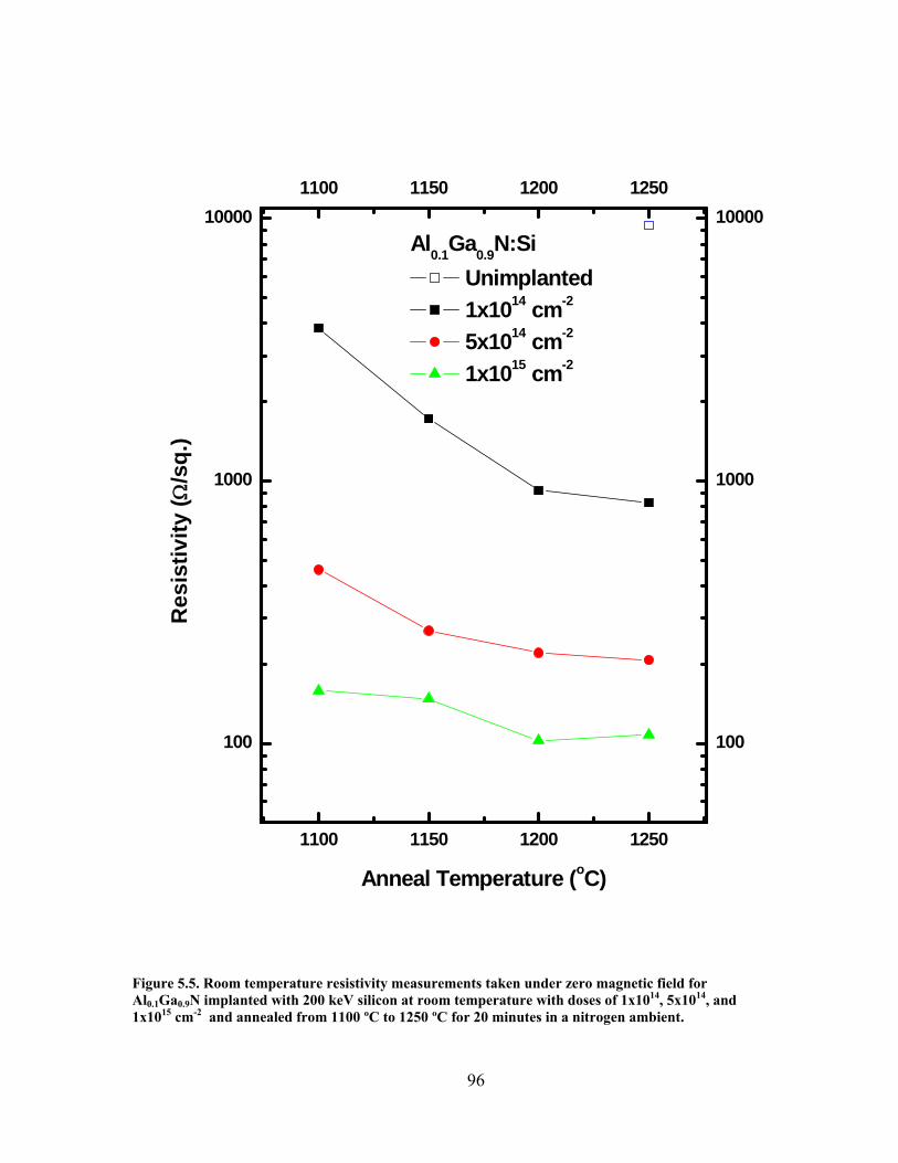
1100 1150 1200 1250
1100 1150 1200 1250
100
1000
10000
100
1000
10000
Res
istiv
ity (Ω
/sq.
)
Anneal Temperature (oC)
Al0.1Ga0.9N:Si Unimplanted 1x1014 cm-2
5x1014 cm-2
1x1015 cm-2
Figure 5.5. Room temperature resistivity measurements taken under zero magnetic field for Al0.1Ga0.9N implanted with 200 keV silicon at room temperature with doses of 1x10¹⁴, 5x10¹⁴, and 1x1015 cm-2 and annealed from 1100 ºC to 1250 ºC for 20 minutes in a nitrogen ambient.
96

97
improvement. The measured resistivities of the higher-dose implanted samples are well
below 1 k Ω/. The samples implanted with 5x1014 cm-2 silicon ions show a dramatic
decrease in resistivity between the 1100 and 1150 ºC anneal and then only show a small
decrease for the rest of the anneal temperature span. The resistivities for these samples
drop from 460 Ω/ after being annealed at 1100 ºC to 208 Ω/ after the 1250 ºC anneal.
The Al0.1Ga0.9N implanted with the high silicon dose exhibited an only a small decrease
in resistivity from the 1100 ºC anneal to the 1150 ºC anneal before decreasing at a much
larger rate for the 1200 ºC anneal. The samples implanted with 1x1015 cm-2 silicon ions
had resistivities of 158 Ω/ and 103 Ω/ after being annealed at 1100 and 1200 ºC,
respectively. The resistivity for the samples implanted with the highest silicon dose
increases slightly to 108 Ω/ after being annealed at 1250 ºC. This increase in resistivity
could be caused by an increase in defects in the crystal lattice from the high temperature
anneal. When the high and low dose silicon implanted Al0.1Ga0.9N experience their
lowest resistivity values, they also have their maximum carrier concentrations, and thus
activations. This is not true for the samples implanted with 5x1014 cm-2 silicon ions;
however, the difference in resistivity between the highest activation anneal temperature
(1200 ºC) and anneal temperature that produces the lowest resistivity (1250 ºC) is only 14
Ω/.
When choosing a material for device applications, the carrier concentration as
well as the mobility is an important aspect of a material to consider. The mobilities for
the Si-implanted Al0.1Ga0.9N annealed for 20 minutes at various temperatures are shown
in Figure 5.6. Room temperature mobility values for Si-implanted GaN have been
reported to be as high as 250 cm2/V·s for samples implanted with a dose of 1x1013 cm-2

1100 1150 1200 1250
1100 1150 1200 1250
0
10
20
30
40
50
60
70
80
90
100
110
0
10
20
30
40
50
60
70
80
90
100
110
Hal
l Mob
ility
(cm
2 /V.s
)
Anneal Temperature (oC)
Al0.1Ga0.9N:Si Unimplanted 1x1014 cm-2
5x1014 cm-2
1x1015 cm-2
Figure 5.6. The room temperature mobility values obtained from the Hall measurements on Al0.1Ga0.9N implanted with 200 keV silicon at room temperature with doses of 1x10¹⁴, 5x10¹⁴, and 1x1015 cm-2 and annealed from 1100 to 1250 ºC for 20 minutes in a nitrogen ambient.
98

99
silicon ions and annealed at 1350 ºC for 17 seconds (22). The reported mobility values
for Al0.1Ga0.9N to date are not as high. Irokawa et al. observed mobility values of 48, 63,
and 65 cm2/V·s for Al0.13Ga0.87N implanted with a dose of 1x10¹⁴, 5.2x10¹⁴, and 1x10¹⁵
cm-2 silicon ions, respectively, and annealed for 5 minutes at 1375 ºC (34). Ryu et al. had
a mobility value of 89 cm2/V·s for Al0.14Ga0.86N implanted with a dose of 1x1014 cm-2
silicon ions after annealing at 1250 ºC for 20 minutes (35). The mobilities determined for
Al0.1Ga0.9N implanted with similar doses in this study are found to be higher than those
reported.
The mobilities of each set of samples increase as the anneal temperature is
increased, with the only exception being the Al0.1Ga0.9N implanted with the lowest dose
and annealed at 1250 ºC where the mobility declines by about 4% of the value following
the 1200 ºC anneal. This decrease in mobility for the Al0.1Ga0.9N implanted with 1x10¹⁴
cm-2 silicon ions and annealed at 1250 ºC can be attributed to an increase in ionized
impurity scattering, which signifies that the lattice damage associated with the ion
implantation has been repaired. The mobility increases in spite of an increase in the
number of ionized impurities indicating that the recovery of the crystal lattice is more
pertinent to the mobility value than ionized impurity scattering. The unimplanted sample
annealed for 20 minutes at 1250 ºC had a mobility value of 103 cm2/V·s. The Al0.1Ga0.9N
implanted with the lowest implantation dose of 1x1014 cm-2 silicon ions has the highest
observed mobilities of the three doses studied, as expected. The mobility values increase
almost linearly from 59 to 109 cm2/V·s as the temperature is increased from 1100 to 1200
ºC. The mobility for these samples then decreases slightly to 103 cm2/V·s, the same as
the unimplanted sample, as the anneal temperature is increased to 1250ºC, at which the
activation for this dose is a maximum and the resistivity is a minimum. The samples

100
implanted with a dose of 5x1014 cm-2 silicon ions show an increase in mobility of about
the same magnitude between the 1100-1150 ºC range and the 1200-1250 ºC range,
however, the change in mobility between 1150 and 1200 ºC is less than 4 cm2/V·s. The
mobilities Al0.1Ga0.9N implanted with this dose increases from 53 to 90 cm2/V·s as the
temperature increases from 1100 to 1250 ºC. Again, anneal temperature for the peak
mobility does not correspond to that of the peak activation. In this case, the mobility
increase can be attributed to a decrease in ionized impurity scattering caused by the
decrease in activation efficiency or that more of the ion implantation induced damage has
been repaired with the higher temperature anneal. The high dose Si-implanted samples,
like the samples implanted with 5x1014 cm-2 silicon ions, show the same magnitude of
mobility change for the 1100-1150 ºC range and the 1200-1250 ºC range, however, the
change in mobility between 1150 and 1200 ºC is a much larger 30 cm2/V·s. The peak
mobility for the Al0.1Ga0.9N implanted with a silicon dose of 1x1015 cm-2 is 76 cm2/V·s
after being annealed at 1250 ºC for 20 minutes. These samples have low mobility values
(~45cm2/V·s) for anneal temperatures (1100-1150 ºC) that produce the higher electrical
activations, and high mobility values at 1200 and 1250 ºC when the activation is low.
One could expect the opposite to be true since the inactive Si and residual damage serve
as scattering centers which would degrade the mobility. However in this case, the
ionized impurity scattering from higher carrier concentrations limits the mobility at lower
anneal temperatures. As the anneal temperature is increased the carrier concentration
declines significantly, reducing the effects of scattering from ionized impurities, which is
reflected as an increase in the mobility. Overall, the mobilities obtained in this study are
higher than most other values reported in the literature to date.
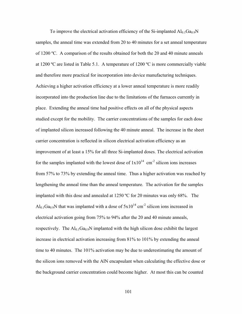
101
To improve the electrical activation efficiency of the Si-implanted Al0.1Ga0.9N
samples, the anneal time was extended from 20 to 40 minutes for a set anneal temperature
of 1200 ºC. A comparison of the results obtained for both the 20 and 40 minute anneals
at 1200 ºC are listed in Table 5.1. A temperature of 1200 ºC is more commercially viable
and therefore more practical for incorporation into device manufacturing techniques.
Achieving a higher activation efficiency at a lower anneal temperature is more readily
incorporated into the production line due to the limitations of the furnaces currently in
place. Extending the anneal time had positive effects on all of the physical aspects
studied except for the mobility. The carrier concentrations of the samples for each dose
of implanted silicon increased following the 40 minute anneal. The increase in the sheet
carrier concentration is reflected in silicon electrical activation efficiency as an
improvement of at least a 15% for all three Si-implanted doses. The electrical activation
for the samples implanted with the lowest dose of 1x1014 cm-2 silicon ions increases
from 57% to 73% by extending the anneal time. Thus a higher activation was reached by
lengthening the anneal time than the anneal temperature. The activation for the samples
implanted with this dose and annealed at 1250 ºC for 20 minutes was only 68%. The
Al0.1Ga0.9N that was implanted with a dose of 5x1014 cm-2 silicon ions increased in
electrical activation going from 75% to 94% after the 20 and 40 minute anneals,
respectively. The Al0.1Ga0.9N implanted with the high silicon dose exhibit the largest
increase in electrical activation increasing from 81% to 101% by extending the anneal
time to 40 minutes. The 101% activation may be due to underestimating the amount of
the silicon ions removed with the AlN encapsulant when calculating the effective dose or
the background carrier concentration could become higher. At most this can be counted

102
Table 5.1. Room temperature Hall Effect results for Al0.1Ga0.9N implanted with three doses of silicon ions that had an energy of 200 keV and annealed at 1200 ºC for 20 and 40 minutes in flowing nitrogen.
Dose
(cm-2) Time (min.)
Carrier Concentration
(cm-2)
Activation (%)
Resistivity (Ω/)
Mobility
(cm2/V·s)
1x10¹⁴ 20 5.57x10¹³ 56.78 920.48 109.19
1x10¹⁴ 40 7.13x10¹³ 72.68 792.03 101.28
5x10¹⁴ 20 3.66x10¹⁴ 74.52 221.72 75.63
5x10¹⁴ 40 4.61x10¹⁴ 93.86 190.24 70.32
1x10¹⁵ 20 7.93x10¹⁴ 80.78 102.64 76.11
1x10¹⁵ 40 9.95x10¹⁴ 101.43 95.85 64.35
as 100% activation, which is a an improvement over the 91% activation achieved for the
sample implanted with this dose after annealing at 1150 ºC for 20 minutes.
The resistivity of the Si-implanted Al0.1Ga0.9N improved about 15% for the
samples implanted with the lowest silicon dose and only about 7% for the samples
implanted with the highest dose of silicon ions. The Al0.1Ga0.9N implanted with 1x10¹⁴
cm-2 silicon ions exhibited a resistivity drop from 920 Ω/ to 792 Ω/ after extending the
anneal time to 40 minutes. This resistivity is lower than the resistivity obtained from
these samples after annealing at 1250 ºC for 20 minutes. The resistivity of the samples
implanted with 5x1014 cm-2silicon ions improved to 190 Ω/from 222 Ω/ after
increasing the anneal time to 40 minutes and annealing at 1200 ºC. The Al0.1Ga0.9N
implanted with this silicon dose and annealed at 1250 ºC for 20 minutes produced a
slightly lower resistivity of 208 Ω/. The Al0.1Ga0.9N implanted with 1x1015 cm-2 silicon
103
ions exhibit a small decrease in resistivity from 103 to 96 Ω/ after increasing the anneal
time to 40 minutes. This is a slight decrease from the samples implanted with this dose
that were annealed for 20 minutes at 1250 ºC that had a resistivity of 108 Ω/.
Lengthening the anneal time to 40 minutes at a lower anneal temperature improved the
resistivities for the Al0.1Ga0.9N that were obtained after annealing at both 1200 and
1250 ºC for the 20 minutes.
The mobility values for the Al0.1Ga0.9N show a slight decrease after lengthening
the anneal time from 20 to 40 minutes, which can be attributed to an increase in the
number of ionized impurities that serve as scattering centers and degrade the mobility.
The samples implanted with the lower doses both show about a 7% drop in mobility
between the two anneals. The samples implanted with 1x1014 cm-2 silicon ions show a
drop from their peak mobility of 109 to 101 cm2/V·s after being annealed at 1200 ºC for
20 and 40 minutes, respectively. The mobility obtained for the sample that were
annealed for 40 minutes is lower than the mobility achieved for the sample implanted
with this silicon dose and annealed at 1250 ºC anneal for 20 minutes, which was 103
cm2/V·s. The Al0.1Ga0.9N implanted with the middle dose of 5x1014 cm-2 silicon ions,
exhibited a mobility drop from 76 to 70 cm2/V·s after extending the anneal time to 40
minutes, which is much lower than the peak mobility of 90 cm2/V·s obtained for the
samples implanted with this silicon dose after being annealed at 1250 ºC for 20 minutes.
The most dramatic decline in mobility was 16% from the peak mobility of 76 cm2/V·s
for the Al0.1Ga0.9N implanted with 1x1015 cm-2 silicon ions after lengthening the anneal
time to 40 minutes.
Most Si-implanted Al0.1Ga0.9N samples achieved high silicon electrical activation
efficiencies above 70% for each implantation dose. The samples implanted with the low

104
silicon dose had the lowest overall activation, reaching 68% for the 20 minute 1250 ºC
anneal and 73% activation after being annealed at 1200 ºC for 40 minutes. The samples
implanted with 5x1014 cm-2 silicon ions reached an activation of 75% after being
annealed for 20 minutes at 1200 ºC, which improved to 94% by extending the anneal
time to 40 minutes. The Al0.1Ga0.9N implanted with the highest dose had the best
activation of 100% following the 1200 ºC anneal for 40 minutes. The samples implanted
with this silicon dose also had considerable activation of 91% following the 1150 ºC
anneal for 20 minutes. Lowering the anneal temperature and lengthening the anneal time
benefited all the material parameters for the Si-implanted Al0.1Ga0.9N except for the
mobility which is due to the increased number of ionized donors, thus implying that the
lattice damage has been fully recovered for all the implanted samples after annealing at
1200 ºC for 20 minutes.
Temperature-Dependent Hall Effect Measurements
Temperature-dependent Hall Effect measurements were taken on the Al0.1Ga0.9N
samples that were annealed at 1200 ºC for 20 minutes in flowing nitrogen to determine
the nature of the carriers as a function of temperature as well as to determine the
ionization energy of the implanted silicon ions. The sheet carrier concentration as a
function of temperature from 10 to 700 K for the samples implanted with each of the
three silicon doses and annealed at 1200 ºC for 20 minutes are shown in Figure 5.7. To
display the temperature-dependent carrier concentration more conveniently, the x-axis is
displayed as 1000/T and split at 20-30 K-1 (50-33 K) to expand the high temperature
regime. The carrier concentrations for all the Al0.1Ga0.9N implanted with each of the
three silicon doses remain relatively constant as the temperature increased from 10 to 50

105
K. The carrier concentration for the samples implanted with the two lower doses of
1x10¹⁴ and 5x1014 cm-2 silicon ions begin to decrease around 50 K, reaching a minimum
at 140 and 300 K, respectively, before increasing continuously to 700 K. The samples
implanted with a dose of 1x1015 cm-2 silicon ions have a relatively constant carrier
concentration at lower temperatures, and increasing gradually over the measured
temperature range. The temperature-independent nature of the carrier concentration
indicates that the implanted silicon ions have formed a degenerate impurity band in the
band gap. A non-degenerate semiconductor would experience carrier freeze out at low
temperatures and the carrier concentration would thus decrease, which is not observed in
the temperature-dependent data for these samples. According to Look, the absence of a
decline in the carrier concentration is due to conduction taking place in the donor level
rather than in the conduction band (72, 113). The critical doping density of Al0.1Ga0.9N is
calculated from equation 2.18 to be 1.83x1018 cm-3. This is the density at which the
material undergoes a Mott transition and most of the donors become ionized independent
of the temperature. The predicted peak carrier concentrations determined from TRIM
calculations for the three implantation doses of 1x10¹⁴, 5x10¹⁴, and 1x1015 cm-2 silicon
ions are 5.62x10¹⁸, 2.81x10¹⁹, and 5.62x1019 cm-3, respectively. All three of the
implanted doses create volume carrier concentrations that exceed the critical Mott
concentration of Al0.1Ga0.9N which explains the metallic-like behavior of the samples.
The Al0.1Ga0.9N implanted with the highest silicon dose has the most temperature
independent carrier concentration as would be expected since this silicon dose produces
the most degenerate samples. The carrier concentration for the lower Si-implanted dose
dips between 100 and 500 K signifying the presence of a multi-channel conduction band,
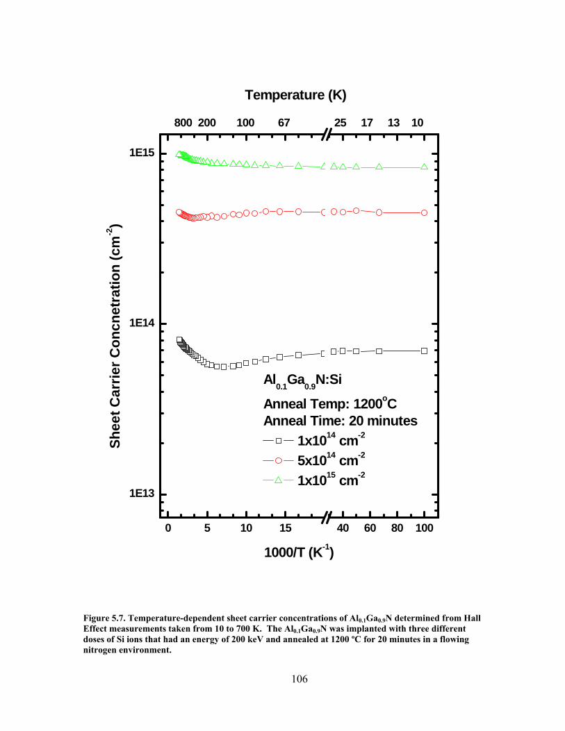
0 5 10 15 40 60 80 100
1E13
1E14
1E15
Temperature (K)
Al0.1Ga0.9N:Si
Anneal Temp: 1200oCAnneal Time: 20 minutes
1x1014 cm-2
5x1014 cm-2
1x1015 cm-2
Shee
t Car
rier C
oncn
etra
tion
(cm
-2)
1000/T (K-1)
800 200 100 67 25 17 13 10
Figure 5.7. Temperature-dependent sheet carrier concentrations of Al0.1Ga0.9N determined from Hall Effect measurements taken from 10 to 700 K. The Al0.1Ga0.9N was implanted with three different doses of Si ions that had an energy of 200 keV and annealed at 1200 ºC for 20 minutes in a flowing nitrogen environment.
106

107
one being the degenerate impurity band and the other the non-degenerate n-type
Al0.1Ga0.9N layer that results from the Gaussian distribution of the implanted ions (37,
68). The samples implanted with 5x1014 cm-2 silicon ions also have a slight dip in the
carrier concentration only at higher temperatures.
As the sample temperature is increased one would expect the carrier concentration
to approach a constant as all the donor electrons become excited into the conduction
band. However, the temperature-dependent carrier concentration for samples implanted
with all three silicon doses begins to increase as the sample temperature approaches 800
K. This sudden increase, along with the dip in carrier concentration for the samples
implanted with the lower silicon doses, indicates the presence of more than one
conducting layer in the material. The dip in the carrier concentration around 140 and
300 K for the samples implanted with 1x10¹⁴ and 5x1014 cm-2 silicon ions is similar to the
temperature-dependent carrier concentrations observed by Look et el. in highly
degenerate GaN samples grown on sapphire substrates with a sputtered ZnO buffer layer
(37). They modeled the dependency using a two-layer Hall effect model and attributed
the conduction to the GaN layer as well as the interfacial region between the GaN and
sapphire substrate.
The temperature-dependent nature of the carrier concentration indicates that the
samples have transitioned from activated conduction to metallic like conduction. This
signifies that the donor impurity level of the silicon has formed into a degenerate band
and as the carrier concentration of the samples increases this impurity band merges with
the conduction band. The effects of impurity screening are enhanced by an increase in
the concentration of ionized donors and will act to reduce the donor ionization energy.
Thus the ionization energy for silicon in Al0.1Ga0.9N can not be accurately estimated from

108
the implanted samples in this study. For the sake of comparison with other literature, the
extracted ionization energies for the three implanted silicon doses in Al0.1Ga0.9N that
were annealed at 1200 ºC are shown in Figure 5.8.
The reported values for the ionization energy of silicon in Al0.1Ga0.9N are on the
order of 1-30 meV. Irokawa et al. reported an ionization energy of 23 meV for
Al0.13Ga0.87N implanted with 1x1014 cm-2 silicon ions and annealed at 1300 ºC for 5
minutes in a nitrogen ambient (34). This energy is consistent with other reported values
for Si ionization energy in AlxGa1-xN with this Al concentration for in-situ doped material
(38-40). Polyakov et al. reported ionization energies on the order of 10 to 16 meV for
AlxGa1-xN with Al concentrations of 10 to 20% (36). While Ryu et al. achieved
ionization energies as low as 1.4 meV and 3.1 meV for Al0.18Ga0.82N that had been
implanted with 5x1014 cm-2 silicon ions and annealed at 1150 ºC and 1250 ºC,
respectively, for 25 minutes in a nitrogen ambient (35). Hwang et al. show that from a
simple hydrogen model, the donor ionization energy of silicon in AlxGa1-xN increases
from 34 to 90 meV as the Al mole fraction is increased from zero to one for a non-
degenerate sample (51).
The ionization energy of the implanted Si ions is determined by assuming that the
carrier concentration is proportional to exp(-ΔE/kBT) for high temperatures. In the low
temperature regime, the ionization energy can then be extracted from the slope of a least
squares fit of the data graphed as the ln(sheet carrier concentration) versus 1/T, which is
referred to as an Arrhenius plot (72,113). The resistivity has a temperature dependence
that is the reciprocal that of the carrier concentration so that resistivity data can also be

1.5 2.0 2.5 3.0 3.5 4.0 4.5 5.0
13.8
14.0
14.2
14.4
14.6
14.8
15.0
15.2
Ed= 3.6 meV
Ed= 1.6 meV
Ln(s
heet
car
rier c
oncn
etra
tion)
1000/T (K-1)
Al0.1Ga0.9N:Si
Anneal Temp: 1200 oCAnneal Time: 20 minutes
1x1014cm-2
5x1014cm-2
1x1015cm-2
Ed= 1.2 meV
Temperature (K)700 500 400 333 285 250 222 200
Figure 5.8: Arrhenius plot used to calculate the ionization energy of the implanted Si for all three doses in Al0.1Ga0.9N. The samples were annealed at 1200 ºC for 20 minutes in a nitrogen ambient. The ionization energies are calculated from the slope of the fit to the Hall data and are shown by the black line.
109

110
used for extracting the ionization energy. The carrier concentration data used for the fit
spanned the temperature range from 200 to 700 K.
The Al0.1Ga0.9N implanted with 1x1014 cm-2 silicon ions exhibits the highest
ionization energy of 3.6 meV of all the implanted silicon doses studied however, this
energy is lower than expected due to degeneracy. The samples implanted with doses of
5x10¹⁴ and 1x1015 cm-2 silicon ions have similar ionization energies of 1.6 and 1.2 meV,
respectively. These empirically determined ionization energies are much lower than
those predicted by Hwang et al. and those reported in the literature due to the degeneracy
of the samples (51). However, they agree well with the results that were reported by Ryu
et al. (35). The actual ionization energy can only be determined if the impurity band is
non-degenerate. The low ionization energy can be attributed to the formation of a
degenerate impurity band caused from exceeding the Mott concentration of 1.8x1018 cm-3
with the implanted silicon doses. The ionization energy levels become shallower as the
implanted silicon doses are increased revealing the higher degeneracy of the samples,
similar to that observed by Fellows in Si-implanted GaN (22).
The temperature-dependent Hall mobilities for the Si-implanted Al0.1Ga0.9N are
shown in Figure 5.9. The samples implanted with each of the three of the silicon doses
exhibit a peak in their mobility curve around 300 K, with the lowest dose exhibiting the
highest mobility of 109 cm2/V·s. The mobility curves for all the Si-implanted Al0.1Ga0.9N
increase as the temperature is raised from 10 to 300 K, at which point they reach their
maximum. The samples implanted with 1x1014 cm-2 silicon ions exhibit the greatest
change in mobility over the given temperature range initially increasing sharply and then
experiencing a more subtle decline. The samples implanted with 5x10¹⁴ and 1x1015 cm-2

0 100 200 300 400 500 600 700 8000
10
20
30
40
50
60
70
80
90
100
110
120
M
obili
ty (c
m2 /V
-s)
Temperature (K)
Al0.1Ga0.9N:Si
Anneal Temp: 1200oCAnneal Time: 20 minutes
1x1014 cm-2
5x1014 cm-2
1x1015 cm-2
Figure 5.9. Temperature-dependent Hall mobilities taken from 10 to 700 K for Al0.1Ga0.9N implanted at room temperature at different doses of silicon ions that had an energy of 200 keV and annealed at 1200 ºC for 20 minutes.
111
112
silicon ions have mobilities very close together, however the mobility is higher for the
Al0.1Ga0.9N implanted with 1x1015 cm-2 silicon ions, as it was for the room temperature
mobility for these samples. The sudden increase in the mobility for the samples
implanted with a dose of 1x1015 cm-2 silicon ions is attributed a decrease in ionized
impurity scattering resulting from the decrease in activation efficiency for the samples
annealed at 1200 °C. These samples a weaker temperature-dependence than the samples
implanted with the lower silicon dose. In general, the mobility decreases as the dose is
increased due to the stronger effects of ionized impurity and polar phonon lattice
scattering. However, at low temperatures (< 100 K), the mobility behavior changes and
begins to increase as the Si-implanted dose is increased. The mobility of non-degenerate
semiconductors should approach zero as the sample temperature is brought down to
absolute zero and then increase rapidly as the temperature is raised due to screening of
ionized impurity scattering that is dominant. The Al0.1Ga0.9N mobilities for the three
implanted silicon doses of 1x10¹⁴, 5x10¹⁴, and 1x1015 cm-2 are 37.3, 46.1, and 47.9
cm2/V·s, respectively, at a temperature of 10 K. The degenerate impurity band causes the
low temperature mobility to be temperature-independent and also to increase with the
doping level. The temperature-dependent mobility curve for the Al0.1Ga0.9N implanted
with the lowest silicon dose most resembles that which is predicted by theory for a non-
degenerate sample. The higher dose curves are more flat and temperature independent as
would be expected by a degenerate sample.
Figure 5.10 shows the temperature-dependent resistivities of the Al0.1Ga0.9N
samples for all three silicon implantation doses. The resistivity decreases significantly as
the implantation dose is increased and also becomes more temperature-independent. All

0 20 40 60 80 10010
100
1000
Al0.1Ga0.9N:Si
Anneal Temp: 1200oCAnneal Time: 20 minutes
1x1014 cm-2
5x1014 cm-2
1x1015 cm-2
Shee
t Res
istiv
ity (Ω
/sq.
)
1000/T (K-1)
Temperature (K)800 100 50 25 17 13 10
Figure 5.10. Temperature-dependent resistivity values calculated from Hall measurements taken from 10 to 700 K for Al0.1Ga0.9N that had been implanted with 1x10¹⁴, 5x10¹⁴, and 1x1015 cm-2 silicon ions at 200 keV and annealed at 1200 ºC for 20 minutes in flowing nitrogen.
113

114
three implantation doses show a relative temperature-independent resistivity from around
10 to 50 K before slowly dipping to a minimum at around 300 K followed by an increase
up through sample temperatures of 700 K. The drop in the resistivity for the samples
implanted with 1x1014 cm-2 silicon ions being the most pronounced and the drop in the
samples implanted with 1x1015 cm-2 silicon ions being almost unnoticeable. The increase
in the resistivity for high temperatures is a result of the dramatic decrease in the mobility
at this temperature range which results from an increase in ionized impurity scattering.
The bend in the resistivity around 300 K for each dose is a manifestation of the
resistivity’s dependence on the mobility, which is dependant on different scattering
mechanisms at different temperatures and thus changes considerably with temperature.
Experiencing a minimum resistivity and a maximum mobility at room
temperature can be beneficial for device performance considering this temperature is the
most common temperature at which devices are required to function. The temperature
independent nature of the carrier concentration, mobility and resistivity as well as the low
ionization energies reveal that the samples increasingly become more degenerate as the
Si-implanted dose is increased from 1x10¹⁴ to 1x1015 cm-2.
Low Temperature Cathodoluminescence Measurements
Cathodoluminescence (CL) measurements were taken with an electron energy of
10 keV with 50 µA of source current. The temperature in the chamber was 7.4 K, and the
slits on the spectrometer were 200 µm both at the entrance and the exit. The range
scanned was 1800 to 7000 Å with a step size of 2 Å and an integration time of 0.1

115
second. The CL spectra give insight into the nature of the energy transitions taking place
in the material, and therefore give the type of defect and impurity levels that may occur in
the band gap.
The spectra of the unimplanted samples shown as a function of anneal
temperature are given in Figure 5.11. To gauge the level of damage recovery in the Si-
implanted samples, the behavior of the unimplanted samples must first be observed. The
dominant feature in AlxGa1-xN luminescence at low temperatures is found to involve the
transition of a localized exciton (44, 60-61). Each of the CL spectra for the given anneal
temperatures show a strong neutral-donor-bound exciton (Do,X) peak at 3.69 eV. The
spectrum for these samples also exhibits a small peak at 3.61 eV, whose source is
unknown. The spectrums for the samples annealed at 1100 and 1150 ºC have been
reduced by a factor of two. The sample annealed for 20 minutes at 1150 ºC has the
strongest intensity followed by the sample annealed at 1100 ºC. The intensity of the
(Do,X) peak at first increases with temperature peaking after the 1150 ºC anneal.
However, increasing the temperature further results in decreasing the (Do,X) intensity.
The sample annealed at 1250 ºC for 20 minutes exhibits the lowest intensity however; the
peak is still very sharp. The reason for the decrease in the intensity of the (Do,X) peak
for this sample are unknown, probably due to the nature of the particular sample, but it is
noticed that the unimplanted sample that was annealed at 1250 ºC was the only
unimplanted sample that had a measurable carrier concentration. The CL spectra for the
unimplanted samples indicate that 1150 ºC is the optimal annealing temperature for
repairing defects that occurred during growth.

2 3 4 5 6
Wavelength (nm)
3.61 eV
x1/2
1250 oC
1150 oC
Unimplanted Al0.1Ga0.9NT = 7.4K
Lum
ines
cenc
e In
tens
ity (a
rb. u
nits
)
Photon Energy (eV)
1100 oC
3.69 eV
700 500 400 300 250 200 180
x1/2
Figure 5.11. CL spectra taken at 7.4 K for unimplanted Al0.1Ga0.9N that have been anneal at 1100, 1150 and 1250 ºC for 20 minutes in flowing nitrogen.
116

117
The low temperature CL spectra, for the silicon implanted Al0.1Ga0.9N annealed
for 20 minutes at 1150 ºC, are shown in Figure 5.12. The spectrum for the unimplanted
sample is 1/20th of its original intensity and shows a sharp (Do,X) peak at 3.69 eV. The
intensities of the (Do,X) peaks for the implanted Al0.1Ga0.9N decrease as the silicon dose
is increased, due to the increased number of donors in the degenerate level. The sample
implanted with a dose of 1x1014 cm-2 silicon ions showed the strongest (Do,X) peak at
3.69 eV, with a shoulder on the lower energy side at 3.61 eV. The spectrum also shows a
broad yellow band (YL) with a peak around 2.4 eV that is not observed in the
unimplanted samples, similar to that observed in GaN (22). Also, this YL band shows
interference patterns. The samples implanted with 5x1014 cm-2 silicon ions exhibit a
similar spectrum only the (Do,X) peak and YL band have weaker intensity. The (Do,X)
peak in the spectrum of the sample implanted with 1x1015 cm-2 silicon ions is much
broader than those for the other implanted doses. The (Do,X) peak is blueshifted to 3.60
eV and has broadened both toward lower and higher energies. The luminescence of this
sample covers a range from 3.5 to 4.0 eV. The near band edge broadening on the low
energy side of the (Do,X) peak or the sample implanted with 1x1015 cm-2 silicon ions is
due to band tailing effects.
These effects are small but are noticeable for the Al0.1Ga0.9N implanted with the
lower silicon doses. The impurity band formation, which was confirmed by the
temperature-dependent Hall effect measurements, can cause random band-edge effects
such as band tailing and band filling. Only the samples implanted with the highest silicon
dose of 1x1015 cm-2 had a volume carrier concentration high enough for band filling to
occur. This effect is seen in the CL spectrum as broadening of the (Do,X) peak towards
higher energies, which is only present in the spectrum of this sample.

2 3 4 5 6
700600 500 400 300 200
Si-Implanted Al0.1Ga0.9N
Anneal: 1150 oC / 20 min.T = 7.4K
Unimplanted
1x1015 cm-2
5x1014 cm-2
1x1014 cm-2
Lu
min
esce
nce
Inte
nsity
(arb
. uni
ts)
Energy (eV)
x1/20
Wavelength (nm)
3.69 eV
2.4 eV
Figure 5.12. CL spectra taken at 7.4 K for Al0.1Ga0.9N that have been anneal at 1150 ºC for 20 minutes in flowing nitrogen.
118
119
The YL band for the Al0.1Ga0.9N implanted with a dose of 1x1015 cm-2 silicon ions
is not as intense as it was in the spectra of the samples implanted with other doses. The
observed YL band decreases as the Si-implanted dose of the Al0.1Ga0.9N is increased (and
therefore activation efficiency) and also as the anneal temperature is increased, which can
be seen in Figure 5.13. There is still much debate over the origin of the yellow band in
GaN and in AlxGa1-xN materials in the literature. Glaser et al. claim the band is the result
of radiative recombination between deep donors and shallow acceptors (41). While
others like Ogino et al. attribute the band to transitions from native shallow donors and
deep carbon related acceptors (42). Polyakov et al. noticed that the peak of the yellow
band shifts to higher energy as the Al concentration of the material is increased. They
claim that it is consistent with a recombination process between native donor defects and
a defect in the middle of the band gap, possibly carbon related (43). Nam et al. also
noticed this shift in the YL band to a violet band, VL, as the Al mole fraction was
increased from 0 to 1 (44). They attribute the formation of this band to DAP transitions
that involve shallow donors, either Si or oxygen, whose ionization energies increase with
increasing Al content and a deep acceptor whose energy does not change with mole
fraction, such as an Al or Ga vacancy or vacancy complex.
The low temperature CL spectra for the silicon implanted Al0.1Ga0.9N annealed
for 20 minutes at 1250 ºC are shown in Figure 5.13. The spectrum of the unimplanted
sample has a strong (Do,X) peak at 3.69 eV with intensity higher than the samples
implanted with 1x10¹⁴ and 5x1014 cm-2 silicon ions. However, as seen in Figure 5.11, the
intensity of the (Do,X) peak for the unimplanted sample annealed at 1250 ºC is
significantly reduced from that of the unimplanted samples annealed at lower
temperatures. The sample implanted with the highest silicon dose exceeds the intensity
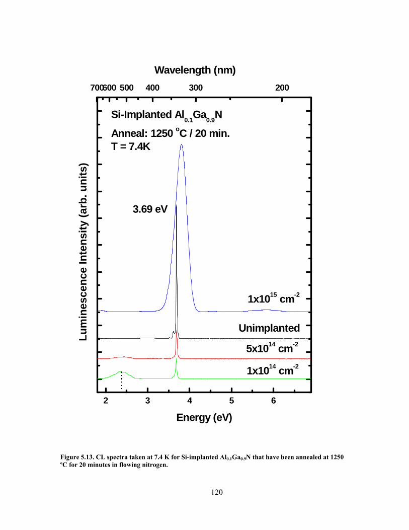
2 3 4 5 6
700600 500 400 300 200
Unimplanted
1x1015 cm-2
5x1014 cm-2
Lum
ines
cenc
e In
tens
ity (a
rb. u
nits
)
Energy (eV)
Si-Implanted Al0.1Ga0.9N
Anneal: 1250 oC / 20 min.T = 7.4K
1x1014 cm-2
3.69 eV
Wavelength (nm)
Figure 5.13. CL spectra taken at 7.4 K for Si-implanted Al0.1Ga0.9N that have been annealed at 1250 ºC for 20 minutes in flowing nitrogen.
120

121
of the unimplanted sample after the 1250 ºC anneal however, the peak has broadened
considerably due to band tailing and band filling effects. At this anneal temperature,
1250 ºC, the intensity of the (Do,X) peak increases slightly as the implantation dose in
increased, which is a little different from what occurred for the 20 minute 1150 ºC anneal.
The sample implanted with 1x1014 cm-2 silicon ions has a sharp (Do,X) peak at 3.69 eV
however, the intensity is weak and band tailing effects are barely noticeable as is for the
samples implanted with a dose of 5x1014 cm-2 silicon ions. The YL band that was
prominent in the spectrum for the 1150 ºC anneal has also lost most of its intensity after
the higher temperature anneal. The YL band is barley distinguishable for the Al0.1Ga0.9N
implanted with 5x1014 cm-2 silicon ions and is no longer visible for the samples implanted
with the highest silicon dose after the 1250 ºC anneal. The spectrum of the samples
implanted with a dose of 5x1014 cm-2 silicon ions exhibits a sharp (Do,X) peak at 3.69 eV
with weaker intensity than the unimplanted sample. The sample implanted with 1x10¹⁵
cm-2 silicon ions has a broad peak centered on 3.80 eV that is as intense as the
unimplanted sample. The peak is more intense and broader than the peak observed for
the 1150 ºC anneal. The YL band luminescence has also been quenched after the high
temperature anneal for the sample implanted with this silicon dose.
The samples annealed at 1250 ºC produce clear spectra that more closely resemble those
of the unimplanted samples, signifying greater recovery of the crystal lattice structure.
The low temperature CL spectra for the Al0.1Ga0.9N implanted with 1x1014 cm-2
silicon ions annealed for 20 minutes at various temperatures are shown in Figure 5.14.
All of the samples result in spectra with sharp (Do,X) peak centered at 3.69 eV. The
(Do,X) peak is very weak for the samples annealed at 1100 ºC but increases rapidly as the
anneal temperature is increased. Apparently, an anneal temperature of 1100 ºC is too low

2 3 4 5 6
x1/4
x1/2
2.4 eV
1200 oC
Si-Implanted Al0.1Ga0.9N
1x1014 cm-2
T = 7.4K
1100 oC
1150 oC
1250 oC
Lum
ines
cenc
e In
tens
ity (a
rb. u
nits
)
Energy (eV)
x1/2
3.69 eV
Wavelength (nm)700 500 400 300 200
Figure 5.14. CL spectra taken at 7.4 K for Al0.1Ga0.9N that has been implanted with 1x1014 cm-2 silicon ions and then annealed at various temperatures for 20 minutes in flowing nitrogen.
122

123
for significant recovery of the implantation induced damage to occur. The spectrum of
the sample annealed at 1250 ºC has been reduced by a factor of 4, and the spectra for the
samples annealed at 1150 and 1200 ºC have been reduced be a factor of 2. The increase
in intensity of the (Do,X) peaks observed for the other anneal temperatures of 1150,
1200, and 1250 ºC indicate that more of the implanted silicon ions have become
electrically active, and successive improvement in the crystal recovery has taken place
with each increase in the anneal temperature.
The YL band in the spectra for the sample annealed at 1100 ºC is barely
observable but quickly becomes prevalent following the 1150 ºC anneal. The YL band
declined in intensity as the anneal temperature was increased from 1150 to 1250 ºC. The
YL band is believed to be caused from transition of a shallow donor and a deep acceptor.
The shallow donor level has been theorized to be the result of silicon or oxygen
impurities in the crystal. The YL band was not observed in any of the spectrum of the
unimplanted samples, even after annealing at 1250 ºC, so that its origin it not believed to
be caused from annealing related defects. The YL band for the samples implanted with
1x1014 cm-2 silicon ions is most prominent is samples that exhibited low activation
efficiency and decreases as the activation of the samples increased. The YL band could
then be attributed to the residual damage from the ion implantation or from the silicon
ions.
These CL results agree very well with the electrical data obtained from Hall
Effect measurements for this implanted silicon dose. The sharpness and strong intensity
of the peak correlate well with the high mobility values obtained on this sample. The
exciton peak and the high mobilities (page 94) observed on the samples implanted with
the low silicon dose indicate excellent implantation damage recovery after annealing at
124
1200 ºC for 20 minutes in flowing nitrogen. This is supported by the decrease in mobility
for the samples annealed at 1250 ºC, which results from an increase in ionized impurity
scattering whose effects can be observed once the lattice damage has been recovered.
The CL spectra of the samples annealed at temperatures from 1100 to 1250 ºC
and implanted with a silicon dose of 5x1014 cm-2 are shown in Figure 5.15. The strongest
(Do,X) peak is observed for the sample annealed at 1150 ºC for 20 minutes. The spectrum
for this sample has been reduced by a factor of twelve. An anneal temperature of
1100 ºC was not sufficient enough to restore a significant amount of lattice damage
caused by the ion implantation. The (Do,X) peak at 3.69 eV in the CL spectrum of this
sample is barely observable and matched in intensity to the YL band. However,
increasing the anneal temperature 50 ºC enhances the exciton peak 200 times signifying a
considerable amount of damage recovery has taken place. The unimplanted sample
annealed at 1150 ºC also exhibited the most intense (Do,X) peak. Increasing the
temperature any further causes the (Do,X) peak to diminish considerably. The YL band
decreases slightly as the temperature is raised from 1150 to 1200 ºC however the YL
band luminescence gets stronger following the 1250 ºC anneal. The peak for the sample
annealed at 1250 ºC is weak and broad showing evidence of band tailing and band filling
effects. The peak is redshifted from the (Do,X) peak to 3.61 eV, which was evident in the
spectrum of the unimplanted samples as a small peak, and is matched in intensity to the
YL band.
The CL spectra would indicate that the optimum anneal temperature for the
(Do,X) signal in the samples that were implanted with this silicon dose is 1150 ºC
whereas the room temperature electrical data indicates that complete lattice damage
recovery takes place after annealing at 1200 ºC. The peak electrical activation efficiency

2 3 4 5 6
x1/12
x1/6
Si-Implanted Al0.1Ga0.9N
5x1014 cm-2
T = 7.4K
3.69 eV
1200 oC
1150 oC
1250 oC
1100 oC
Energy (eV)
Lum
ines
cenc
e In
tens
ity (a
rb. u
nits
)
x1/4
Wavelength (nm)700 500 400 300 200
Figure 5.15. CL spectra taken at 7.4 K for Al0.1Ga0.9N that has been implanted with 5x1014 cm-2 silicon ions and then annealed at various temperatures for 20 minutes in flowing nitrogen.
125

126
for samples implanted with this dose occurred after the samples were annealed at
1200 ºC. Increasing the anneal temperature to 1250 ºC causes the activation to decrease
which in turn causes a decrease in ionized impurity scattering which allows the mobility
to increase. This is also witnessed in the time-dependent annealing in which the
activation efficiency increases after lengthening the anneal time, but the mobility
decreases due to the increase in ionized impurity scattering. As mentioned previously,
the effects of ionized impurity scattering are weaker then those of the lattice recovery and
as a result are normally not witnessed until lattice recovery has taken place. Thus the
electrical data indicates that the lattice damage has been restored after annealing at 1200
ºC. The YL band decreases slightly as the anneal temperature is raised which could
possibly be attributed to an increase in activation. This line of thinking would also
explain the increase in the YL band as the anneal temperature is increased to 1250 ºC.
The decline in intensity of the (Do,X) peak could be due to the silicon ions forming
trapping centers that are charged but are non-radiative. The broadening and redshifting
of the peak in the sample annealed at 1250 ºC could be due to a new transition that is
compensating.
The CL spectra of the Al0.1Ga0.9N implanted with the highest silicon dose of
1x1015 cm-2 are shown in Figure 5.16. As the anneal temperature is increased, the
intensity of the (Do,X) peak increases significantly. The samples annealed at lower
temperatures, where the silicon electrical activation was at its maximum, show very weak
(Do,X) peak. The sample annealed at 1100 ºC has a weak (Do,X) peak at 3.69 eV and a
slightly observable YL band. The (Do,X) peak is observable for the sample that had been
annealed at 1150 ºC, but it is not sharp. The dominant luminescence from this sample
has broadened considerably to cover the range 3.5 to 4.1 eV. The YL band is enhanced

2 3 4 5 6
x 1/102.4 eV
Si-Implanted Al0.1Ga0.9N
1x1015 cm-2
T = 7.4K
Lum
ines
cenc
e In
tens
ity (a
rb. u
nits
)
Energy (eV)
1100 oC
1150 oC
1200 oC
1250 oC
3.80 eV
3.69 eV
Wavelength (nm)700 500 400 300 200
Figure 5.16. CL spectra taken at 7.4 K for Al0.1Ga0.9N that has been implanted with 1x1015 cm-2 silicon ions and then annealed at various temperatures for 20 minutes in flowing nitrogen.
127

128
in the sample annealed at 1150 ºC from the sample annealed at 1100 ºC. The sample
annealed at 1200 ºC show recovery of the (Do,X) centered at 3.69 eV that is sharp but
weak when compared to the intensity of the sample annealed at 1250 ºC whose spectrum
has been reduced by a factor of 10. As the anneal temperature is increased to 1250 ºC,
the band edge peak is broadened considerably due to band tailing and band filling and its
peak occurs at a higher energy of 3.80 eV. However, the (Do,X) peak appears clearly
after annealing at 1200 ºC and also the full width half max of the peak is improved upon
extending the anneal temperature to 1200 ºC. The decrease in the full width half max of
the peak observed when increasing the anneal temperature to 1200 ºC is lost upon raising
the anneal temperature to 1250 ºC. The intensity of the peak annealed at 1250 ºC
supersedes that of all the other anneal temperatures. The YL band for these samples
increases as the anneal temperature is increased from 1100 to 1200 ºC and then
disappears for the sample that was annealed at 1250 ºC. Thus the YL band does not
decrease as the activation increases as it has for the samples implanted with the lower
silicon doses.
The optical data indicates the optimal annealing temperature for Al0.1Ga0.9N
implanted with 1x1015 cm-2 silicon ions would be 1200 ºC considering that this is the
only sample that displays a sharp (Do,X) peak, like the as-grown material. The weak
intensity could be related to the decline in the activation efficiency that occurred for the
sample annealed at this temperature. As the anneal temperature is increased the silicon
ions begin to occupy nitrogen sites and thus begin to compensate the electrons donated to
the conduction by the silicon ions that are on gallium or aluminum sub-lattice positions.
The electrical data indicates that the lattice damage has been greatly restored after
annealing at 1150 or 1200 ºC. The sample that obtained the highest activation efficiency

129
was annealed at 1150 ºC and based on the changes of the mobility for the other annealing
temperatures (increasing from decrease in activation for the 1200 and 1250 ºC anneals
and decreasing from an increase in activation from the extended time anneals at 1200 ºC)
it would appear that the optimal annealing temperature was 1150 ºC. However, the
mobility and the spectral response are weaker than expected if the majority of the lattice
damage has been recovered. When considering all of the data, the optimal annealing
temperature for Al0.1Ga0.9N implanted with 1x1015 cm-2 silicon ions must be 1200 ºC.
In the latter two implantation doses the CL spectrum exhibiting the most lattice
damage recovery does not correspond to the anneal temperature that produces the best
silicon activation. The increased activation at lower anneal temperatures in the samples
implanted with the higher silicon doses is attributed to an increase in the implantation
damage which creates more vacancies and thus a place in the lattice for the implanted Si
ions. The samples implanted with the lowest silicon doses experience the least amount of
radiation damage and exhibits the best lattice recovery yet the lowest silicon electrical
activation.
Silicon Implanted Al0.2Ga0.8N
AlxGa1-xN with Al concentrations around 20% have been less investigated by
other groups than Al0.1Ga0.9N. The most comprehensive studies have come from Ryu et
al. who have shown great success implanting silicon at various doses into MBE-grown
AlxGa1-xN with Al concentrations of 18 and 24 % (35, 45-46). The Al0.18Ga0.82N was
implanted with Si ions at 200 keV with doses of 5x10¹⁴ and 1x1015 cm-2. These samples
were annealed at 1250 ºC for 25 minutes and exhibited 100% and 94% electrical

130
activations, respectively. They found the electrical activation efficiencies to be strongly
dependent on anneal time as well as anneal temperature. In their study, they focused on
annealing at lower temperatures and slowly increasing the anneal time to show that time
variation can have a greater impact on the activation and produce more commercially
viable results. The same group implanted Al0.24Ga0.76N with silicon ions at 200 keV with
doses of 5x10¹³ and 1x1014 cm-2. The Al0.24Ga0.76N exhibited nearly 100% activation for
both doses following a 20 minute anneal at 1350 and 1300 ºC, respectively. Another
study, conducted by Chitwood achieved 65% and 87% activation for MBE-grown
Al0.25Ga0.75N implanted with silicon ions at 200 keV for doses of 1x10¹⁴ and 1x1015 cm-2,
respectively, after annealing at 1350 ºC for 2 minutes (47). Researchers have found that
even with an Al mole fraction of 20%, AlxGa1-xN material’s resistive properties can be
hard to overcome. Nakano et al. implanted Al0.2Ga0.8N with oxygen ions that had an
energy of 83 keV in a dose of 5.8x1014 cm-2 and found the material too resistive to collect
data even after annealing at 1300 ºC for 5 minutes in flowing nitrogen (48). However,
this was not the case for the Si-implanted Al0.2Ga0.8N grown by MEMOCVD used in this
study.
Room Temperature Hall Effect Measurements
The MEMOCVD grown Al0.2Ga0.8N was capped with 500Å of AlN and
implanted at room temperature with Si ions that had an energy of 200 keV with three
different doses. The Si doses were 1x10¹⁴, 5x10¹⁴, and 1x1015 cm-2 and the effective
doses are 9.84x10¹³, 4.92x10¹⁴, and 9.84x1014 cm-2, respectively when taking into
account the AlN cap. The samples were annealed from 1150 to 1300 ºC for 20 minutes

131
in a flowing nitrogen environment. The Al0.2Ga0.8N samples experienced minor damage
to the surface morphology following the anneal at 1300 ºC, increasing the anneal
temperature to 1350 ºC however, caused significant damage to the surface for these
samples. Annealing at 1200 ºC for 40 minutes also produced highly damaged samples
that had visible amounts of liquid gallium and aluminum on the surface, however during
the anneal the sample lifting rod malfunctioned which extended the sample decent
considerably. Room temperature Hall effect measurements were conducted to determine
sheet carrier concentrations for the samples and the results are shown in Figure 5.17. The
unimplanted samples both as-grown and annealed were highly resistive making it
impossible to collect any meaningful data. Thus, the silicon electrical activation was
calculated using the measured room temperature carrier concentration with no correction
for background carriers.
The sheet carrier concentrations for the Al0.2Ga0.8N implanted with each silicon dose
respond uniformly to an increase in the anneal temperature. The carrier concentrations
for these samples increase as the anneal temperature is increased from 1150 to 1300 ºC,
with the samples implanted with the lowest silicon dose experiencing the most dramatic
incline across the given temperature span. The Al0.2Ga0.8N implanted with 1x1014 cm-2
silicon ions exhibit a large increase in carrier concentration between the 1150 and 1200
ºC anneal, after which it increases linearly as the temperature is increased from 1200 to
1300 ºC. The maximum carrier concentration obtained for the samples implanted with
this silicon dose was 8.25x1013 cm-2 following an anneal at 1300 ºC for 20 minutes in a
nitrogen ambient. The carrier concentrations for the Al0.2Ga0.8N samples implanted with
doses of 5x10¹⁴ and 1x1015 cm-2 silicon ions have the same dependence on the anneal
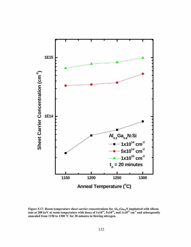
1150 1200 1250 1300
1E14
1E15
Al0.2Ga0.8N:Si
1x1014 cm-2
5x1014 cm-2
1x1015 cm-2
Sh
eet C
arrie
r Con
cent
ratio
n (c
m-2)
Anneal Temperature (oC)
tA = 20 minutes
Figure 5.17. Room temperature sheet carrier concentrations for Al0.2Ga0.8N implanted with silicon ions at 200 keV at room temperature with doses of 1x10¹⁴, 5x10¹⁴, and 1x1015 cm-2 and subsequently annealed from 1150 to 1300 ºC for 20 minutes in flowing nitrogen.
132

133
temperature. The carrier concentrations for both samples increase linearly as the anneal
temperature is raised from 1150 to 1250 ºC and then spikes for the samples annealed at
1300 ºC. The maximum carrier concentrations obtained for the Al0.2Ga0.8N implanted
with silicon doses of 5x10¹⁴ and 1x1015 cm-2 were 5.33x10¹⁴ and 9.92x1014 cm-2,
respectively, after being annealed for 20 minutes at 1300 ºC.
The AlxGa1-xN with Al mole fractions of 10 and 20% implanted with a silicon
dose of 1x1014 cm-2 have carrier concentrations that increase steadily as the anneal
temperature is raised however, the Al0.1Ga0.9N samples exhibit slightly higher carrier
concentrations at any given temperature. The carrier concentrations for the AlxGa1-xN
implanted with a dose of 5x1014 cm-2 silicon ions also show similar dependencies on the
anneal temperature between the two Al mole fractions. The Al0.1Ga0.9N, however,
decreased in carrier concentration after being annealed at 1250 ºC; whereas the
Al0.2Ga0.8N samples continued to show increasing carrier concentrations for anneal
temperatures up to 1300 ºC. The AlxGa1-xN samples implanted 5x1014 cm-2 silicon ions,
unlike the samples implanted with 1x1014 cm-2, have higher carrier concentrations for the
Al0.2Ga0.8N than Al0.1Ga0.9N at any given temperature. The samples implanted with
1x1015 cm-2 exhibit the most remarkable change in behavior between the two different Al
concentrations. The Al0.1Ga0.9N samples reached their peak carrier concentration after
being annealed at 1150 ºC, and further increasing the anneal temperature caused the
carrier concentration to decline. The carrier concentrations of the Al0.2Ga0.8N, however,
are enhanced as the anneal temperature is increased from 1150 to 1300 ºC.
The silicon electrical activations, shown in Figure 5.18, of these samples are
closely related to the carrier concentrations and follow the same trends with the anneal
temperature as mentioned above. The electrical activation efficiency for Al0.2Ga0.8N was
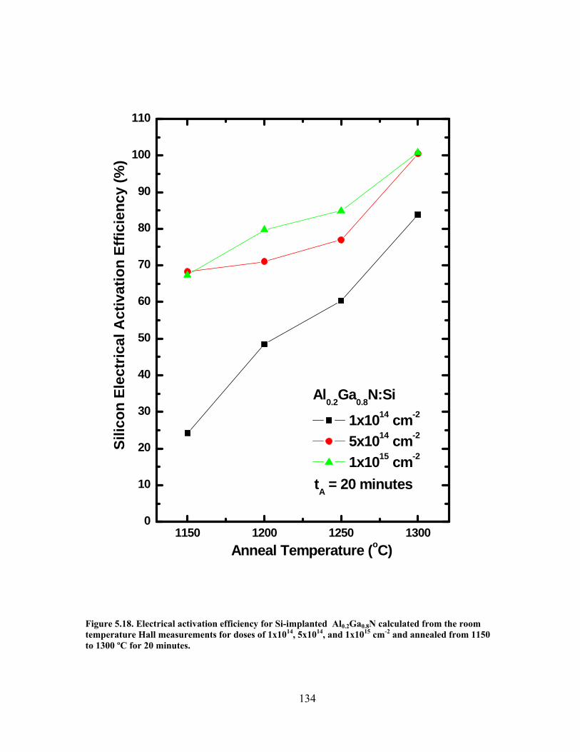
1150 1200 1250 13000
10
20
30
40
50
60
70
80
90
100
110
Al0.2Ga0.8N:Si
1x1014 cm-2
5x1014 cm-2
1x1015 cm-2
Silic
on E
lect
rical
Act
ivat
ion
Effic
ienc
y (%
)
Anneal Temperature (oC)
tA = 20 minutes
Figure 5.18. Electrical activation efficiency for Si-implanted Al0.2Ga0.8N calculated from the room temperature Hall measurements for doses of 1x10¹⁴, 5x10¹⁴, and 1x1015 cm-2 and annealed from 1150 to 1300 ºC for 20 minutes.
134

135
calculated using the effective dose and room temperature sheet carrier concentrations.
Higher implantation doses resulted in higher silicon activation efficiencies for anneal
temperatures up to 1300 ºC. The silicon electrical activation for the samples implanted
with 1x1014 cm-2 silicon ions exhibits the most improvement over the given temperature
range, increasing from 24% to 83% after being annealed for 20 minutes at 1150 ºC and
1300 ºC. The samples implanted with a dose of 5x1014 cm-2 silicon ions have a
significant activation efficiency of 68% after the 1150 ºC twenty minute anneal and
steadily increases to a maximum of 100% following the 1300 ºC anneal. The samples
implanted with the highest silicon dose of 1x1015 cm-2 also reaches 100% activation after
being annealed at 1300 ºC for 20 minutes in a nitrogen ambient.
The increased activation for the samples implanted with the higher doses is
attributed to an increase in the implantation damage which creates more vacancies to
better incorporate the implanted Si ions. The samples implanted with the lowest dose
experience the least amount of radiation damage and exhibit the best lattice recovery
however; they have the lowest silicon electrical activation.
The Al0.1Ga0.9N implanted with all three silicon doses display their peak electrical
activations at different anneal temperatures while the Al0.2Ga0.8N exhibit their peak
activation at 1300 ºC for all the implanted silicon doses. The samples implanted with the
highest silicon dose generally exhibit the best activations for both Al mole fractions at
any given anneal temperature. The AlxGa1-xN implanted with the lowest silicon dose had
the lowest activations but showed the best response to an increase in anneal temperature,
indicating that a further increase in the anneal temperature may result in higher
activation. Like the Al0.1Ga0.9N, the higher implanted silicon doses are more readily
activated than lower silicon doses in Al0.2Ga0.8N, which is illustrated in Figure 5.19.

1E14 1E15
1E14
1E15
Sh
eet C
arrie
r Con
cent
ratio
n (c
m-2)
Actual Implanted Si Dose (cm-2)
Al0.2Ga0.8N:Si
1150 oC/ 20min. 1200 oC/ 20min. 1250 oC/ 20min. 1300 oC/ 20min.
100 % Activation
Figure 5.19. The room temperature sheet carrier concentrations versus the actual implantation dose for Al0.2Ga0.8N implanted at room temperature with silicon at 200 keV with doses of 1x10¹⁴, 5x10¹⁴, and 1x1015 cm-2 and annealed from 1150 to 1300 ºC for 20 minutes in a nitrogen ambient.
136

137
The Al0.2Ga0.8N implanted with 1x1014 cm-2 silicon ions exhibits an electrical
activation of 83% following a 1300 ºC anneal for 20 minutes in flowing nitrogen. Ryu et
al. reported a slightly higher activation of ~100% for Si-implanted MBE-grown
Al0.24Ga0.76N under the same implantation and anneal conditions, while Chitwood
achieved only 65% after annealing at 1350 ºC for 2 minutes (35, 47). The Al0.2Ga0.8N
implanted with a silicon dose of 5x1014 cm-2 reach a maximum electrical activation of
100% after being annealed at 1300 ºC for 20 minutes. Ryu reported the same activation
for Al0.24Ga0.76N implanted with the same silicon dose after annealing at 1250 ºC for 25
minutes. In this study, the electrical activation of the Al0.2Ga0.8N implanted with 1x10¹⁵
cm-2 silicon ions was 100% following a 20 minute anneal at 1300 ºC. Ryu reported an
activation of 94% for similar samples after annealing at 1250 for 25 minutes while,
Chitwood only reported an 87% activation after annealing Al0.25Ga0.75N at 1350 ºC for
two minutes. The optimal anneal temperature for the Al0.2Ga0.8N implanted with a dose
of 1x1014 cm-2 silicon ions may be higher than 1300 ºC, while the optimal anneal
temperature for the samples implanted with the higher silicon doses of 5x10¹⁴ and 1x10¹⁵
cm-2 is 1300 ºC for an anneal time of 20 minutes. The optimal anneal temperature is
found to be dose dependent, requiring higher anneal temperatures as the ion dose is
decreased to achieve high electrical activation.
The resistivity values for the Al0.2Ga0.8N implanted with each silicon dose are
shown in Figure 5.20. The resistivity of all the samples decreased as the anneal
temperature was increased. The samples implanted with a dose of 1x1015 cm-2 silicon
ions exhibit the least improvement in resistivity over the given temperature span and the
samples implanted with a silicon dose 1x1014 cm-2 show the greatest. The samples
implanted with a dose of 1x1014 cm-2 silicon ions have resistivity values 10 and 24 times

1150 1200 1250 13000
100
200
300
400
500
600
700
1000
1500
2000
2500
3000
3500
4000
4500
Al0.2Ga0.8N:SitA=20 min
1x1014 cm-2
5x1014 cm-2
1x1015 cm-2
R
esis
tivity
(Ω/s
q.)
Anneal Temperature (oC)
Figure 5.20. Room temperature resistivity measurements taken under zero magnetic field for Al0.2Ga0.8N implanted at room temperature with silicon ions at 200 keV with doses of 1x10¹⁴, 5x10¹⁴, and 1x1015 cm-2 and annealed from 1150 ºC to 1300 ºC for 20 minutes in a nitrogen ambient.
138

139
higher than the samples implanted with 5x10¹⁴ and 1x1015 cm-2 silicon ions after being
annealed at 1150 ºC for 20 minutes. However, the resistivity for the samples implanted
with this silicon dose decreases 3.2 kΩ/ as the anneal temperature is increased to 1300
ºC. The largest measured resistivity is 4.2 kΩ/ for the samples implanted with 1x10¹⁴
cm-2 silicon ions after being annealed at 1150 ºC for 20 minutes. The measured
resistivities of the samples implanted with 5x10¹⁴ and 1x1015 cm-2 silicon ions are all
below 500 Ω/. The Al0.2Ga0.8N implanted with 5x1014 cm-2 silicon ions show a linear
decrease in resistivity over the entire temperature span dropping from 403 Ω/ to
214 Ω/. The samples implanted with 1x1015 cm-2 silicon ions also show a linear
decrease in resistivity as the anneal temperature is increased from 1150 to 1300 ºC
dropping from 176 Ω/ to 115 Ω/, respectively. The anneal temperature that produces
the lowest resistivity in Al0.2Ga0.8N is also the anneal temperature that corresponds to the
maximum in carrier concentration, and thus activation efficiency for all of the implanted
Al0.2Ga0.8N. The resistivity, for both the 10 and 20% AlxGa1-xN, of the implanted
samples was found to increase as the silicon dose was lowered from 1x1015 cm-2 to
1x1014 cm-2 silicon ions, which is consistent with that of the carrier concentration.
The room temperature mobilities for each dose of the Si-implanted Al0.2Ga0.8N
samples are shown in Figure 5.21. The mobility for all the samples increased as the
anneal temperature was increased up to 1250 ºC, and then declines at an anneal
temperature of 1300 ºC. The mobility of the samples implanted 1x1014 cm-2 silicon ions
had much higher mobilities than the samples implanted with the two higher silicon doses
due to an increase in ionized impurity scattering for the higher dose implanted samples.
The samples implanted with 1x1014 cm-2 silicon ions show a dramatic rise in mobility
from 62 cm2/V·s to 98 cm2/V·s as the anneal temperature is increased from 1150 to

1150 1200 1250 130030
40
50
60
70
80
90
100
110
Al0.2Ga0.8N:Si
1x1014 cm-2
5x1014 cm-2
1x1015 cm-2
Mob
ility
(cm
2 / V-s
)
Anneal Temperature (oC)
tA=20 min
Figure 5.21. The room temperature mobility values obtained from Hall measurements on Al0.2Ga0.8N implanted at room temperature with silicon at 200 keV with doses of 1x10¹⁴, 5x10¹⁴, and 1x1015 cm-2 and annealed from 1150 to 1300 ºC for 20 minutes in a nitrogen ambient.
140
141
1250 ºC. After being annealed at 1300 ºC the mobility for the samples implanted with
this silicon dose decreases to 76 cm2/V·s, slightly lower than the mobility obtained for the
samples annealed at 1200 ºC. The samples implanted with silicon doses of 5x10¹⁴ and
1x1015 cm-2 show a linear increase in mobility as the temperature is raised from 1150 to
1250 ºC, with the mobilities of the samples implanted with 5x1014 cm-2 silicon ions being
higher for any given anneal temperature. The peak mobilities for the samples implanted
with the two highest silicon doses are 63 and 55 cm2/V·s, respectively. After being
annealed at 1300 ºC, the mobilities for the Al0.2Ga0.8N implanted with these silicon doses
drop to 54 cm2/V·s. The decrease in the mobility for the Al0.2Ga0.8N annealed at 1300 ºC
is caused by impurity scattering becoming dominant over defect scattering, considering
the peak activation for each of the samples was achieved after annealing at 1300 ºC. This
implies that lattice damage recovery was complete after annealing at 1250 ºC, whereas
for the Al0.1Ga0.9N this occurred at 1200 ºC.
The observed mobilities, in this study, are similar to those reported by others.
Ryu et al. observed mobilities of are 64 and 62 cm2/V·s for Al0.18Ga0.82N implanted with
doses 5x10¹⁴and 1x1015 cm-2 silicon ions and annealed for 25 minutes at 1200 ºC (35).
They also reported a mobility of 76 cm2/V·s for Al0.24Ga0.76N implanted with a silicon
dose of 1x1014 cm-2 after being annealed at 1300 ºC for 20 minutes. Chitwood observed
mobilities of 28 and 50 cm2/V·s for Al0.25Ga0.75N implanted with doses of 5x10¹⁴ and
1x1015 cm-2 silicon ions after annealing for 2 minutes at 1350 ºC (47). The mobilities for
the Al0.2Ga0.8N implanted with silicon doses of 5x10¹⁴ and 1x1015 cm-2 are comparable to
others findings however, the mobilities obtained for the samples implanted with a dose of
1x1014 cm-2 silicon ions are much higher than those reported to date.

142
Temperature-Dependent Hall Effect Measurements
Temperature-dependent Hall Effect measurements were taken on the Al0.2Ga0.8N samples
that were annealed at 1200 and 1300 ºC for 20 minutes in flowing nitrogen to determine
the nature of the carriers as a function of temperature as well as to determine the
ionization energy of the implanted silicon ions. The sheet carrier concentrations as a
function of temperature from 10 to 700 K for the samples implanted with each of the
three silicon doses and annealed at 1200 and 1300 ºC for 20 minutes are shown in Figure
5.22. The carrier concentrations for all the Al0.2Ga0.8N implanted with each of the silicon
doses remain relatively constant as the temperature increased from 10 to 50 K. The
samples implanted with the two lower doses of 1x10¹⁴ and 5x1014 cm-2 silicon ions
experience a decrease in carrier concentration beginning at 50 K and reaching a minimum
at 100 and 160 K, respectively, before increasing to a higher carrier concentration at
700 K. The samples implanted with a silicon dose of 1x1015 cm-2 have a relatively
constant carrier concentration, only increasing slightly over the measured temperature
range and also reaching a higher carrier concentration at 700 K. The temperature
independent nature of the carrier concentration is similar to that seen for the Al0.1Ga0.9N
samples and indicates that the implanted silicon ions have formed a degenerate impurity
band in the band gap. The critical doping density of Al0.2Ga0.8N calculated from equation
2.18 is found to be 2.35x1018 cm-3. The predicted peak carrier concentrations determined
from TRIM calculations for the three implantation doses of 1x10¹⁴, 5x10¹⁴, and 1x10¹⁵
cm-2 silicon ions are 5.63x10¹⁸, 2.82x10¹⁹, and 5.63x1019 cm-3, respectively. All three
implanted doses have volume carrier concentrations that exceed the critical Mott
concentration, which explains the degenerate nature of the samples.

0 5 10 15 20 25 60 80 100
1E14
1E15
Temperature (K)
Sh
eet C
arrie
r Con
cent
ratio
n (c
m-2)
1000/T(K-1)
Al0.2Ga0.8N:SitA = 20 minutes
1x1015 cm-2
1200 oC 1300 oC
1x1014 cm-2
1200 oC 1300 oC
5x1014 cm-2
1200 oC 1300 oC
800 200 100 70 50 40 20 15 10
Figure 5.22. Temperature-dependent sheet carrier concentrations of Al0.2Ga0.8N determined from Hall Effect measurements taken from 10 to 700 K. The Al0.2Ga0.8N was implanted with three different doses of Si ions at 200 keV and annealed at 1200 and 1300 ºC for 20 minutes in a flowing nitrogen environment.
143

144
The Al0.2Ga0.8N samples implanted with 1x10¹⁴ and 5x10¹⁴ silicon ions undergo a larger
dip in the carrier concentration as the temperature is increased than the Al0.1Ga0.9N. The
samples implanted with the highest silicon dose have the most temperature independent
carrier concentration as would be expected since this dose creates the most degenerate
samples. The carrier concentration for the samples implanted with the lower doses dip
between 100 and 500 K signifying the presence of a multi-channel conduction band, one
being the degenerate layer and the other the non-degenerate layer due to an approximate
Gaussian distribution of the carrier concentration, similar to that reported by Look et al.
(37). The samples implanted with 1x1015 cm-2 silicon ions also have a slight dip in the
carrier concentration which occurs at higher temperatures. Degenerate samples yield
ionization energies lower than the actual energy due to the enhanced effects of impurity
screening as the donor concentration is increased (72). Therefore, the silicon ionization
energy for Al0.2Ga0.8N can not be determined from the samples in this study.
The temperature-dependent hall mobilities for these samples are shown in Figure
5.23. The Al0.2Ga0.8N implanted with the different silicon doses all exhibit a peak in their
mobility curve slightly below 300 K. The sample implanted with 1x1014 cm-2 silicon ions
has the highest mobilities of 82 and 101 cm2/V·s after being annealed for 20 minutes at
1200 and 1300 ºC, respectively. The samples implanted with 5x1014 cm-2 silicon ions
have peak mobilities of 52 and 67 cm2/V·s after being annealed at 1200 and 1300 ºC,
respectively, which are slightly higher than those of the samples implanted with a dose of
1x1015 cm-2 silicon ions. The samples implanted with the highest silicon dose have
mobilities of 40 and 57 cm2/V·s following a 20 minutes anneal at 1200 and 1300 ºC,
respectively. The mobility curves for all the Si-implanted Al0.2Ga0.8N increase as the
sample temperature is increased to about 250 K at which point the mobility begins to

100 200 300 400 500 600 700
10
20
30
40
50
60
70
80
90
100
110
Al0.2Ga0.8N:SitA = 20 minutes
Mob
ility
(cm
2 / V.s
)
Temperature (K)
1200 oC, 1x1014 cm-2
1300 oC, 1x1014 cm-2
1200 oC, 5x1014 cm-2
1300 oC, 5x1014 cm-2
1200 oC, 1x1015 cm-2
1300 oC, 1x1015 cm-2
Figure 5.23. Temperature-dependent Hall mobilities taken from 10 to 700 K for Al0.2Ga0.8N implanted at room temperature with three different doses of silicon ions at 200 keV and annealed at 1200 and 1300 ºC for 20 minutes.
145

146
decline. The mobility curves become more temperature independent as the implanted
silicon dose is increased, exposing the increasingly degenerate nature of the samples.
The degeneracy can also be noticed by the relatively high mobilities observed at 10 K,
where the mobility of a non-degenerate material would approach zero. The mobility for
the samples implanted with doses of 1x10¹⁴, 5x10¹⁴, and 1x1015 cm-2 silicon ions and
annealed at 1200 ºC are 25.9, 35.3, and 36.6 cm2/V·s, respectively, when the samples
temperature is 10 K. These mobilities are all lower than the those for the samples
annealed at 1300 ºC, which are 35.6, 46.9, and 46.7 cm2/V·s for the three doses,
respectively. The degenerate impurity band causes the low temperature mobility to be
temperature independent and is seen here to increase with doping level and also anneal
temperature. The temperature-dependent mobility curve of the samples implanted with
1x1014 cm-2 silicon ions most resembles that which is predicted for a non-degenerate
sample. The mobility curves for the samples implanted with the higher silicon doses are
more flat as would be expected by a degenerate sample.
Figure 5.24 shows the temperature-dependent resistivity of the Al0.2Ga0.8N
samples annealed at 1200 and 1300 ºC for all three implanted silicon doses. The
resistivity of the Al0.2Ga0.8N decreases significantly as the implanted silicon dose is
increased due to an increase in the carrier concentration. The samples implanted with
1x1014 cm-2 silicon ions have a large decrease in resistivity at high temperatures which is
related to the rapid increase in the mobility seen at this temperature range. The resistivity
of the samples implanted with the higher silicon doses are more temperature independent.
The samples for all three implanted silicon doses show a relative temperature
independent resistivity from 10 to 50 K and then they begin to slowly decline to a
minimum around 240-380 K before increasing again as the sample temperature is raised

0 20 40 60 80 1000
100
200
300
400
1000
2000
3000
4000
5000
6000
Temperature (K)
Al0.2Ga0.8N:SitA = 20 minutes
1200 oC, 1x1014 cm-2
1300 oC, 1x1014 cm-2
1200 oC, 5x1014 cm-2
Sh
eet R
eisi
tvity
(Ω/s
q.)
1000/T(K-1)
1300 oC, 5x1014 cm-2
1200 oC, 1x1015 cm-2
1300 oC, 1x1015 cm-2
800 50 25 20 15 10
147
Figure 5.24. Temperature-dependent resistivity values calculated from Hall measurements taken from 10 to 700 K for Al0.2Ga0.8N that had been implanted with 1x10¹⁴, 5x10¹⁴, and 1x1015 cm-2 silicon ions at 200 keV and annealed at 1200 and 1300ºC for 20 minutes in flowing nitrogen.

148
to 700 K. The increase in the resistivity for high temperatures is a result of the dramatic
decrease in the mobility at this temperature range which results from an increase in
ionized impurity scattering. The bend in the resistivity around 300 K for each dose is a
manifestation of the resistivity’s dependence on the mobility, which is dependant on
different scattering mechanisms at different temperatures and thus changes considerably
with temperature.
Low Temperature Cathodoluminescence Measurements
Cathodoluminescence measurements were taken at an electron energy of 10 keV
with 50 µA of source current, the temperature in the chamber was 7.4 K, and the slits on
the spectrometer were 200 µm both at the entrance and the exit. The range scanned was
1800 to 7000 Å with a step size of 2 Å and an integration time of 0.1 second.
To gauge the level of damage recovery in the implanted samples, the behavior of
the unimplanted samples must first be observed. The spectrum of the unimplanted
samples shown as a function of anneal temperature are given in Figure 5.25. The features
of the CL spectra for the unimplanted samples remain undamaged even after annealing at
1300 ºC showing a good (Do,X) peak. However none of the annealed samples have an
intensity as high as that of the as-grown sample, whose CL spectrum has been reduced by
a factor of 80. The as-grown Al0.2Ga0.8N has a (Do,X) peak that is 30 times that of the
unimplanted samples that had been annealed. The CL spectra for the as-grown sample
and those annealed at 1200 and 1300 ºC show a strong neutral-donor-bound exciton
(Do,X) peak at 3.90 eV. The spectrums of the samples annealed at 1200 and 1300 ºC
have been reduced by a factor of 4. The sample annealed for 20 minutes at 1150 ºC has a

2 3 4 5 6
Unimplanted Al0.2Ga0.8NT=7.4 K 3.90 eV
3.78 eV
x 1/80
x 1/4
Wavelength (nm)
As-grown
C
L In
tens
ity (a
rb. u
nits
)
Energy (eV)
1150 oC
1200 oC
1300 oC
700 500 400 300 200
x 1/4
Figure 5.25. CL spectra taken at 7.4 K for unimplanted Al0.2Ga0.8N both as-grown and annealed at 1150, 1200, and 1300 ºC for 20 minutes in flowing nitrogen.
149

150
broad peak with the weakest intensity centered at 3.78 eV. The reasons for the
redshifting and broadening of the peak are unclear. It seems that the low annealing
temperatures have more detrimental effects on the optical properties of the as-grown
material than higher temperature annealing. However, the spectra for the unimplanted
Al0.1Ga0.9N did not exhibit any broadening. In fact, the intensity of the (Do,X) peak
increased as the anneal temperature was increased from 1100 to 1150 ºC, and decreased
upon further elevation of the anneal temperature.
The low temperature CL spectra for the Si-implanted Al0.2Ga0.8N annealed for 20
minutes at 1300 ºC are shown in Figure 5.26. The spectrum of the unimplanted sample
and that of sample implanted with 1x1014 cm-2 silicon ions have been reduced by a factor
of 2. The spectra of all the samples show a sharp (Do,X) peak at 3.90 eV. The (Do,X)
intensity for the samples implanted with 5x10¹⁴ and 1x1015 cm-2 silicon ions are similar
to each other and much weaker than the peak for the sample implanted with 1x1014 cm-2
silicon ions and the unimplanted sample. The decrease in intensity of the (Do,X) peak
could be due to the increased donor concentration as the implanted silicon dose is
increased. The sample implanted with a dose of 1x1014 cm-2 silicon ions show the
strongest (Do,X) peak at 3.90 eV matching the intensity of the unimplanted sample. The
CL spectra for the Al0.2Ga0.8N do not exhibit a broad yellow band (YL) as was seen in the
spectra of the Al0.1Ga0.9N. The samples implanted with 5x1014 cm-2 silicon ions show a
similar spectrum to the samples implanted with the lowest silicon dose, only the intensity
of the (Do,X) peak is much weaker. The features of the spectrum for the samples
implanted with 1x1015 cm-2 silicon ions are similar to the samples implanted with the
other silicon doses however, the peak energy is slightly shifted to higher energies at 3.95
eV, probably due to the effects of band filling.

2 3 4 5 6
Wavelength (nm)
1x1015 cm-2
5x1014 cm-2
x1/2
x1/2
3.90 eV
Si-implanted Al0.2Ga0.8N
Anneal: 1300oC/ 20 min.T=7.4 K
C
L In
tens
ity (a
rb. u
nits
)
Energy (eV)
1x1014 cm-2
Unimplanted
700 500 400 300 200
Figure 5.26. CL spectra taken at 7.4 K for Al0.2Ga0.8N implanted at room temperature with silicon ions at 200 keV with doses of 1x10¹⁴, 5x10¹⁴, and 1x1015 cm-2 and annealed at 1300 ºC for 20 minutes in flowing nitrogen.
151

152
The near band edge broadening on the low energy side of the (Do,X) peak for the
sample implanted with 1x1015 cm-2 silicon ions is due to band tailing effects. These
effects are barely noticeable for the samples implanted with the lower silicon doses. The
Si-implanted doses exceed the Mott concentration of the material which results in random
band-edge effects and band tailing. Only the sample implanted with the highest dose of
1x1015 cm-2 silicon ions has a volume carrier concentration high enough for band filling
to occur, which is seen as broadening of the (Do,X) peak towards higher energies. The
effects of band filling and band tailing are not as noticeable in the CL spectra for the
Al0.2Ga0.8N as they are for the Al0.1Ga0.9N. This is due to the increase in the Mott
concentration as the Al mole fraction of the material is increased.
The low temperature CL spectra for the Al0.2Ga0.8N implanted with 1x1014 cm-2
silicon ions and annealed for 20 minutes at various temperatures are shown in Figure
5.27. All of the anneal temperatures produce a (Do,X) peak in the CL spectra centered at
3.90 eV that broadens as the temperature is decreased. The CL spectra for the samples
annealed at 1200 and 1300 ºC have been reduced by a factor of twenty, while the spectra
for the sample annealed at 1150 ºC was reduced by a factor of two. The samples
implanted with this dose exhibit their best spectra after being annealed at 1300 ºC. The
intensity of this spectrum is only slightly higher than the intensity of the sample annealed
at 1200 ºC. The spectra improve as the anneal temperature is increased except in the case
of the sample annealed at 1250 ºC in which the intensity is noticeably decreased and
evidence of the YL band, seen in the Al0.1Ga0.9N, emerges. The CL intensity of the
samples increases as the anneal temperature is increased signifying successive
improvement in the crystal lattice with each increase in the anneal temperature.

2 3 4 5 6
x1/2
Wavelength (nm)
700 500 400 300 200
x1/20
3.90 eV
1250 oC
1150 oC
1200 oC
1300 oC
Si-implanted Al0.2Ga0.8N
1x1014cm-2
T=7.4 K
C
L In
tens
ity (a
rb. u
nits
)
Energy (eV)
x1/20
Figure 5.27. CL spectra taken at 7.4 K for Al0.2Ga0.8N implanted at room temperature with silicon ions at 200 keV in a dose of 1x1014 cm-2 and annealed at various temperatures for 20 minutes in flowing nitrogen.
153

154
The (Do,X) peak is weak for the samples annealed at 1150 ºC but it increases rapidly as
the anneal temperature is increased. An anneal temperature of 1250 ºC produced
unusually low CL intensity with unknown reason, however an anneal temperature of
1300 ºC produced and excellent peak signifying that the majority of the anneal damage
had been restored as did the 1200 ºC anneal. The increase in intensity of the (Do,X)
peaks observed for all anneal temperatures except 1250 ºC indicate that more of the
implanted silicon ions have become electrically active with an increase in anneal
temperature.
These samples all exhibit their peak carrier concentration after being annealed at
1300 ºC; however the peak mobility occurred for the samples annealed at 1250 ºC. The
decline in mobility was attributed to an increase in ionized impurity scattering, which
occurred since the gain in mobility from the decrease in defect scattering had minimized
(suggesting that the lattice defects had been repaired). Considering this information, the
considerably low intensity of the CL spectrum from the sample annealed at 1250 ºC is
completely unexpected and could be due to experimental error. Otherwise, these CL
spectra agree very well with the electrical activation results obtained from Hall effect
measurements for the samples implanted with this silicon dose. The sharpness and strong
intensity of the (Do,X) peak for the sample annealed at 1300 ºC correlate well with the
high activation efficiencies obtained for this sample. The exciton peak and high
mobilities observed on the samples implanted with 1x1014 cm-2 silicon ions indicate
excellent implantation damage recovery following a 20 minute anneal at 1300 ºC in
flowing nitrogen.

155
The CL spectra of the samples implanted with a silicon dose of 5x1014 cm-2 are
shown in Figure 5.28. The spectra of the samples annealed at 1150, 1250, and 1300 ºC
have all been reduced by a factor of 5. These samples exhibit their strongest (Do,X) peak
after being annealed at 1150 ºC for 20 minutes. The spectrum of the sample annealed at
1200 ºC has the weakest and broadest peak, without an apparent reason. As the anneal
temperature is increased to 1250 and 1300 ºC, the intensity of the (Do,X) peak increases
significantly, almost matching the intensity of the sample annealed at 1150 ºC. Although,
the CL spectra for the samples annealed at 1150 ºC is very strong, the peak electrical
activation efficiency occurred after the samples were annealed at 1300 ºC. The spectrum
of the samples annealed at 1300 ºC also exhibits excellent recovery of the (Do,X) peak,
and is close in intensity and sharpness to the sample annealed at 1150 ºC. The CL spectra
for the Al0.2Ga0.8N implanted with 5x1014 cm-2 silicon ions do not have any yellow
luminescence. All the spectra exhibit a (Do,X) peak with slight broadening on the low
energy side due to band tailing effects.
The CL spectra of the samples implanted with the highest silicon dose of 1x10¹⁵
cm-2 and annealed for 20 minutes at various temperatures are shown in Figure 5.29. All
the samples show recovery of the (Do,X) centered at 3.90 eV and no emergence of yellow
luminescence. As the anneal temperature is increased the intensity of the (Do,X) peak
increases significantly, except in the case of the sample annealed at 1250 ºC. This
spectrum exhibits the weakest intensity and broadest peak of all the anneal temperatures
without clear reason. The intensity of the peak for the samples annealed at 1300 ºC is at
least 5 times more intense than the samples annealed at the lower anneal temperatures.
All the spectra show considerable broadening both towards low and high energies, which

2 3 4 5 6
Wavelength (nm)
x1/5
x1/5
x1/5
3.90 eV
Si-implanted Al0.2Ga0.8N
5x1014cm-2
T=7.4 K
1250 oC
1150 oC
1300 oC
1200 oC
C
L In
tens
ity (a
rb. u
nits
)
Energy (eV)
700 500 400 300 200
Figure 5.28. CL spectra taken at 7.4 K for Al0.2Ga0.8N implanted at room temperature with silicon ions at 200 keV in a dose of 5x1014 cm-2 and annealed at various temperatures for 20 minutes in flowing nitrogen.
156

2 3 4 5 6
Wavelength (nm)
1200 oC
1250 oC
1300 oC
1150 oC
3.90 eV
Si-implanted Al0.2Ga0.8N
1x1015cm-2
T=7.4 K
C
L In
tens
ity (a
rb. u
nits
)
Energy (eV)
700 500 400 300 200
Figure 5.29. CL spectra taken at 7.4 K for Al0.2Ga0.3N implanted at room temperature with silicon ions at 200 keV in a dose of 1x1015 cm-2 silicon ions and then annealed at various temperatures for 20 minutes in flowing nitrogen.
157

158
correlates well with the temperature-dependant data that suggests the samples implanted
with this dose are highly degenerate.
The CL spectrum of the samples implanted with the latter two higher silicon
doses exhibit their most intense (Do,X) peak after being annealed at 1300 ºC for 20
minutes, indicating a greater level of damage recovery. This anneal temperature also
produced the highest activation efficiency and lowest resistivity. The considerable
decrease in intensity of the samples annealed at 1200 and 1250 ºC, respsectively is
curious considering that the electrical data does not show any adverse behavior for this
anneal temperature.
Silicon Implanted Al0.3Ga0.7N
Literature on implanted Al0.3Ga0.7N is limited. Chitwood implanted 1x1015 cm-2
silicon ions into MBE grown Al0.3Ga0.7N and achieved 42 % activation after annealing at
1300 ºC for 2 minutes in flowing nitrogen (47). She also attempted lower implanted
silicon doses but the material quality was poor with visible cracks so that it was
impossible to collect any electrical data. Good quality high Al concentration AlxGa1-xN
epilayers have only become available in recent years (49-50). The MEMOCVD
Al0.3Ga0.7N in this study had excellent surface morphology before and after the high
temperature annealing.
There are no reported ionization energies for silicon implanted Al0.3Ga0.7N.
Hwang et al. calculated the donor ionization energy of AlxGa1-xN from a simple hydrogen
model using low-frequency dielectric constants and found that it increases from 34 meV
to 90 meV as the Al mole fraction is increased from 0 to 1 (51). The theoretical

159
ionization energy for Si in Al0.3Ga0.7N, assuming a linear increase with Al concentration,
would then be on the order of 50 meV for a non-degenerate sample. The implanted
silicon doses of 1x10¹⁴, 5x10¹⁴, and 1x1015 cm-2 correspond to peak volume carrier
concentrations of 5.66x10¹⁸, 2.83x10¹⁹ and 5.66x1019 cm-3, respectively in Al0.3Ga0.7N
which all exceed the Mott concentration of 2.67x1018 cm-3, calculated from equation
2.18, for this material. Therefore, the implanted samples will be degenerate and the
ionization energy for silicon in Al0.3Ga0.7N can not be determined from the samples used
in this study.
Room Temperature Hall Effect Measurements
The MEMOCVD grown Al0.3Ga0.7N was capped with 500Å of AlN and then
implanted at room temperature with Si ions at 200 keV in three different doses. The Si
doses were 1x10¹⁴, 5x10¹⁴, and 1x1015 cm-2 which corresponds to effective doses of
9.87x10¹³, 4.94x10¹⁴, and 9.87x1014 cm-2, respectively after accounting for the AlN
encapsulant. The samples were annealed from 1150 to 1350 ºC for 20 minutes in a
nitrogen environment. The samples exhibited slight edge damage on the surface after
being annealed at 1350 ºC. Room temperature Hall effect measurements were conducted
to determine sheet carrier concentrations for the samples and the results are shown in
Figure 5.30. The unimplanted samples, both as-grown and annealed, were highly
resistive making it impossible to collect any meaningful data. Thus, the silicon electrical
activation was calculated using the measured carrier concentration with no corrections
made for the background carriers.

1150 1200 1250 1300 1350
1E13
1E14
1E15
Al0.3Ga0.7N:Si
1x1014 cm-2
5x1014 cm-2
1x1015 cm-2 Shee
t Car
rier C
once
ntra
tion
(cm
-2)
Anneal Temperature (oC)
tA = 20 minutes
Figure 5.30. Room temperature sheet carrier concentrations for Al0.3Ga0.7N implanted at room temperature with silicon ions at 200 keV with doses of 1x10¹⁴, 5x10¹⁴, and 1x1015 cm-2 and annealed from 1150 to 1350 ºC for 20 minutes in flowing nitrogen.
160

161
The sheet carrier concentrations for Al0.3Ga0.7N implanted with each silicon dose
respond by increasing linearly to an increase in the anneal temperature and exhibit a
small amount of change in magnitude over the given temperature range. The only
exception is the sample implanted with 1x1014 cm-2 silicon ions which exhibits a large
increase as the anneal temperature is raised from 1150 to 1200 ºC. Thus, the samples
implanted with the lowest silicon dose show the most dramatic change in carrier
concentration as the anneal temperature is raised, from 1.4x10¹³ to 6.7x1013 cm-2 for
temperatures 1150 and 1300 ºC, respectively. The carrier concentrations for the
Al0.3Ga0.7N implanted with doses of 5x10¹⁴ and 1x1015 cm-2 silicon ions exhibit similiar
dependence on the anneal temperature. For both samples, the carrier concentration
increases steadily as the anneal temperature is raised from 1150 to 1300 and 1350 ºC,
respectively. The maximum carrier concentration for the samples implanted with 5x10¹⁴
cm-2 silicon ions was 4.43x1014 cm-2 after annealing at 1350 ºC for 20 minutes in a
flowing nitrogen ambient. The Al0.3Ga0.7N implanted with a dose of 1x1015 cm-2 silicon
ions reaches a maximum carrier concentration of 1.08x1015 cm-2 after being annealed for
20 minutes at 1300 ºC.
The dependence of the carrier concentration on the anneal temperature is very
similar for the Al0.1Ga0.9N, Al0.2Ga0.8N and Al0.3Ga0.7N samples. For all the Al mole
fractions, the samples implanted with the higher silicon doses exhibit only a small
variation with the anneal temperature. Only the samples implanted with 1x1014 cm-2
silicon ions show any appreciable change in carrier concentration and just between anneal
temperatures of 1150 and 1200 ºC. The peak carrier concentrations for both Al mole
fractions were achieved after annealing at 1300 ºC for 20 minutes, with the Al0.2Ga0.8N
having higher carrier concentrations at any given ion dose. The Al0.3Ga0.7N implanted

162
with 5x1014 cm-2 silicon ions have carrier concentrations have a 17% decrease in carrier
concentration from the Al0.2Ga0.8N implanted with this dose and annealed at 1300 ºC for
20 minutes, which are 20% lower than the carrier concentrations of the Al0.1Ga0.9N
samples that were annealed for 20 minutes at 1250 ºC. The Al0.3Ga0.7N implanted with
1x1015 cm-2 silicon ions show a 10% decrease in carrier concentration over those
obtained for the Al0.2Ga0.8N under the same anneal conditions. The Al0.2Ga0.8N sample
also shows a 10% improvement over the Al0.1Ga0.9N implanted with this dose and
annealed at 1150 ºC. In general, the carrier concentrations of the AlxGa1-xN with Al
concentrations of 10 to 30% all exhibit similar dependencies on the anneal temperature.
The annealing temperature that produces the highest carrier concentration increases as the
Al mole fraction of the material is increased.
The silicon electrical activation of these samples is closely related to the carrier
concentration and follows the same trends with the anneal temperature as mentioned
above. The electrical activation for the Al0.3Ga0.7N, shown in Figure 5.31, was calculated
using the effective dose and room temperature sheet carrier concentrations. The higher
the implanted silicon dose the higher the activation efficiency for anneal temperatures up
to 1350 ºC. The silicon electrical activation for the samples implanted with 1x1014 cm-2
silicon ions exhibits the most improvement over the given temperature range, increasing
from 14% to 74% after being annealed for 20 minutes at 1150 and 1300 ºC, respectively.
The Al0.3Ga0.7N implanted with the lowest silicon dose experienced the lowest activation
efficiencies but also showed the best response to an increase in anneal temperature,
indicating that a further increase in the temperature may result in higher activation. This
behavior is consistent with the Al0.1Ga0.9N and Al0.2Ga0.8N implanted with this silicon
dose. The samples implanted with a dose of 5x1014 cm-2 silicon ions have a significant

1150 1200 1250 1300 13500
10
20
30
40
50
60
70
80
90
100
110
Anneal Temperature (oC)
tA = 20 minutes
Al0.3Ga0.7N:Si
1x1014 cm-2
5x1014 cm-2
1x1015 cm-2
Si
licon
Ele
ctric
al A
ctiv
atio
n Ef
ficie
ncy
(%)
Figure 5.31. Silicon electrical activation efficiency for Al0.3Ga0.7N calculated from the room temperature Hall measurements for implanted silicon doses of 1x10¹⁴, 5x10¹⁴, and 1x1015 cm-2 and annealed for 20 minutes from 1150 to 1350 ºC.
163

164
70% activation efficiency after being annealed for 20 minutes at 1150 ºC and steadily
increases to a maximum of 90% following the 1350 ºC anneal. The Al0.3Ga0.7N
implanted a silicon dose of 1x1015 cm-2 reaches 100% activation after being annealed at
1300 ºC for 20 minutes in a nitrogen ambient. The Al0.2Ga0.8N samples implanted with
the same dose reach 100% activation under the same annealing conditions, while the
maximum activation for the Al0.1Ga0.9N samples was 94% after a 40 minute anneal at
1200 ºC. The samples implanted with the highest silicon dose exhibited activations of
109% after the 1300 ºC anneal. An electrical activation over 100% could be the result of
over dose implantation or underestimating the effective dose. The AlxGa1-xN with 10 and
20% Al mole fractions implanted with this silicon dose also reached 100% activation
under various annealing conditions. As seen with the AlxGa1-xN with Al mole fractions
of 10 and 20%, the Al0.3Ga0.7N samples implanted with the highest silicon dose are also
more readily activated than those implanted with the lower silicon doses, which is
illustrated in Figure 5.32.
Based on the activation efficiency, the optimal anneal temperature for the
Al0.3Ga0.7N implanted with doses of 1x10¹⁴ and 5x1014cm-2 silicon ions the may be higher
than 1300 and 1350 ºC, respectively. However, 100% activation was achieved for the
sample implanted with the higher silicon dose of 1x1015 cm-2 after annealing at 1300 ºC
for 20 minutes. The optimal anneal temperature is dose dependent, with lower implanted
doses requiring higher temperatures to attain the activations that the high dose implanted
samples achieve at lower anneal temperatures, as was seen for both the Al0.1Ga0.9N and
Al0.2Ga0.8N.
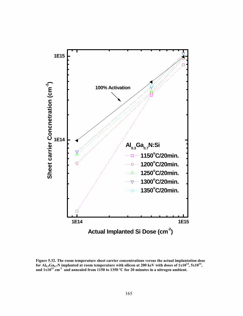
1E14 1E15
1E14
1E15
100% Activation
Actual Implanted Si Dose (cm-2)
Shee
t car
rier C
oncn
etra
tion
(cm
-2)
Al0.3Ga0.7N:Si
1150oC/20min. 1200oC/20min. 1250oC/20min. 1300oC/20min. 1350oC/20min.
Figure 5.32. The room temperature sheet carrier concentrations versus the actual implantation dose for Al0.3Ga0.7N implanted at room temperature with silicon at 200 keV with doses of 1x10¹⁴, 5x10¹⁴, and 1x1015 cm-2 and annealed from 1150 to 1350 ºC for 20 minutes in a nitrogen ambient.
165
166
The resistivities for all the implanted Al0.3Ga0.7N are shown in Figure 5.33. The
low samples implanted with 1x1014 cm-2 silicon ions have a resistivity of 2.57 kΩ/
which is 4 and 8 times higher than the samples implanted with 5x10¹⁴ and 1x1015 cm-2
when annealed at 1150 ºC for 20 minutes. The resistivity for the samples implanted with
the lowest silicon dose falls about 1.3 kΩ/ as the anneal temperature is increased to
1300 ºC. As seen with the Al0.1Ga0.9N and Al0.2Ga0.8N, the resistivity of all the samples
decreases as the anneal temperature is increased, with the samples implanted with the
highest silicon dose showing the least improvement and the samples implanted with the
lowest silicon dose the highest, which is consistent with the carrier concentration. The
measured resistivities of the higher silicon dose implanted Al0.3Ga0.7N are almost all
below 400 Ω/. The samples implanted with 5x1014 cm-2 silicon ions show a rapid
decrease in resistivity as the anneal temperature is increased from 1150 to 1200 ºC and
then begins to decreases linearly as the anneal temperature is brought up to 1350 ºC. The
resistivity for the samples implanted with this dose drop from 666 Ω/ to 221 Ω/ as the
anneal temperature is raised from 1150 to 1350 ºC. The samples implanted with 1x10¹⁵
cm-2 silicon ions showed a slightly linear decrease in resistivity as the anneal temperature
is increased from 1150 to 1300 ºC dropping from 291 Ω/ to 95 Ω/, respectively.
The resistivity of the implanted Al0.3Ga0.7N for each silicon dose is similar to the
resistivity of the corresponding silicon dose in Al0.2Ga0.8N and Al0.1Ga0.9N samples.
However, the overall values of the resistivity have decreased from the previous mole
fractions. Of all the Al concentrations investigated thus far the Al0.3Ga0.7N sample
implanted with 1x1015 cm-2 silicon ions and annealed at 1300ºC for 20 minutes has the
lowest resistivity of 95 Ω/. The anneal temperature that produces the lowest resistivity

1150 1200 1250 1300 13500
200
400
600
1200
1500
1800
2100
2400
2700
Anneal Temperature (oC)
Sh
eet R
eisi
tivity
(Ω/s
q.)
Al0.3Ga0.7N:Si
1x1014 cm-2
5x1014 cm-2
1x1015 cm-2
tA = 20 minutes
Figure 5.33. Room temperature resistivity measurements taken under zero magnetic field for Al0.3Ga0.7N implanted at room temperature with silicon at 200 keV with doses of 1x10¹⁴, 5x10¹⁴, and 1x1015 cm-2 and annealed from 1150 to 1350 ºC for 20 minutes in a nitrogen ambient.
167
168
in the Al0.3Ga0.7N corresponds to the anneal temperature that creates a maximum in
carrier concentration, and thus activation for all of the implanted doses.
Room temperature mobility values for Si-implanted Al0.3Ga0.7N are shown in
Figure 5.34. The mobility increases as the anneal temperature is increased up to 1350 ºC
for each of the implanted samples despite the increased effects of ionized impurity
scattering. The peak activation for each of the samples was achieved after annealing at
1300 ºC or 1350 ºC, which corresponds to the anneal temperature that produces the peak
mobility for each of the samples suggesting that lattice recovery may not be complete
after annealing at these temperatures. In general, the mobility increases as the implanted
silicon dose is increased. However, the reverse it true for the samples annealed at 1150
ºC. The samples implanted with 5x10¹⁴ and 1x1015 cm-2 silicon ions have mobilities that
are very close to one another, and after being annealed at 1300 ºC the samples implanted
with 1x1015 cm-2 silicon ions have a higher carrier concentration. The samples implanted
with 1x1014 cm-2 show a dramatic rise in mobility from 21 cm2/V·s to 64 cm2/V·s as the
temperature is increased from 1150 to 1200 ºC and then begins to increase linearly as the
temperature is raised to 1300 ºC. The mobility for the low-dose implanted Al0.3Ga0.7N
annealed at 1150 ºC decreased more than 40 cm2/V·s from that of the AlxGa1-xN with Al
concentrations of 10 and 20%. After being annealed at 1300 ºC the mobility for these
samples peaks at 76 cm2/V·s.
The mobility for the samples implanted with a dose of 5x10¹⁴ silicon ions increase
throughout the temperature span, more rapidly between the 1150 and 1250 ºC anneal.
These samples reach a peak mobility of 64 cm2/V·s after being annealed for 20 minutes at
1350 ºC. The Al0.1Ga0.9N and Al0.2Ga0.8N implanted with 5x1014 cm-2 silicon ions had
slightly lower peak mobilities of 63 and 55 cm2/V·s, respectively. The mobility of the

1150 1200 1250 1300 1350
20
30
40
50
60
70
80
90
Anneal Temperature (oC)
tA = 20 minutes
Al0.3Ga0.7N:Si
1x1014 cm-2
5x1014 cm-2
1x1015 cm-2
M
obili
ty (c
m2 / V
.s)
Figure 5.34.The room temperature mobility values calculated from Hall measurements on Al0.3Ga0.7N implanted at room temperature with silicon at 200 keV with doses of 1x10¹⁴, 5x10¹⁴, and 1x1015 cm-2 and annealed from 1150 to 1350 ºC for 20 minutes in a nitrogen ambient.
169

170
samples implanted with 1x1015 cm-2 silicon ions increases linearly as the temperature is
raised from 1150 to 1300 ºC, reaching a peak mobility of 61 cm2/V·s. The mobilities for
the Al0.1Ga0.9N and Al0.2Ga0.8N implanted with the same silicon dose are higher, at 90
and 76 cm2/V·s, respectively. The mobilities for the Al0.3Ga0.7N are slightly lower than
the mobilities of t he Al0.1Ga0.9N and Al0.2Ga0.8N. However, the mobilities obtained for
the Al0.3Ga0.7N are much higher than those observed by Chitwood of 35 and 38 cm2/V·s
after annealing at 1300 and 1350 ºC for two minutes (47).
The Si-implanted Al0.3Ga0.7N samples behaved much like the AlxGa1-xN with the
Al mole fractions of 10 and 20%, with all three implanted silicon doses achieving high
electrical activation efficiency. The samples implanted with the lowest silicon dose had
the worst electrical activation and resistivity (74%, 1.3 kΩ/) however, it had the highest
mobility values of 80 cm2/V·s. The samples implanted with a silicon dose of 5x1014 cm-2
reached an activation of 90% after being annealed for 20 minutes at 1300 ºC with
considerably lower resistivity and mobility values of 221 Ω/ and 64cm2/V·s,
respectively. The Al0.3Ga0.7N implanted with the highest silicon dose had the best
activation of 100% and the best resistivity of 95 Ω/ following the 1300 ºC anneal for 20
minutes. The mobility for this dose was 61cm2/V·s.
To improve the silicon electrical activation efficiency of the Si-implanted
Al0.3Ga0.7N samples the anneal time was extended from 20 to 40 minutes for a set anneal
temperature of 1200 ºC. A comparison of the results obtained for both the 20 and 40
minute anneals at 1200 ºC are listed in Table 5.2. A temperature of 1200 ºC is more
commercially viable and therefore more practical for incorporation into device
manufacturing techniques. Extending the anneal time had mixed affects on all of the
physical aspects determined from Hall effect measurements. The carrier concentrations

171
and therefore activation efficiency of the all the implanted samples increased following
the 40 minute anneal. The electrical activation efficiency also increased more with each
successive dose. The resistivity of the samples implanted with 1x10¹⁴ silicon ions
increases 10%, which is related to a decrease in the mobility for these samples. The
samples implanted with 1x1014 cm-2 silicon ions exhibit a small increase in the sheet
carrier concentration which causes a 3% increase in electrical activation efficiency
bringing it up to 56.7%. The mobility for the samples implanted with this silicon dose
decreases from 64.4 cm2/V·s to 54.1 cm2/V·s, due to an increase in ionized impurity
scattering thus suggesting that the lattice damage has been mostly repaired. The
electrical activation for the samples implanted with 5x1014 cm-2 silicon ions increases 8%
to 86% after the 40 minute anneal. The resistivity for the samples implanted with this
dose decreases 17% to 300.5 Ω/ due to the increase in the carrier concentration and
mobility for these samples. The mobility for the samples implanted with 5x1014 cm-2
silicon ions increase 11% to 48.9 cm2/V·s after the extended time anneal despite an
increase in ionized impurity scattering indicating that the lattice damage is not fully
recovered. The samples implanted with 1x1015 cm-2 silicon ions have an activation of
96% following a 20 minute anneal at 1200 ºC, extending the anneal time to 40 minutes
resulted in an increase in the activation to 100%.
The resistivity for these samples decreases less than 35 Ω/. The mobility increased
slightly for the samples implanted with a silicon dose of 1x1015 cm-2 between the two
anneal times from 43 cm2/V·s to 47 cm2/V·s. Like the Al0.3Ga0.7N implanted with
5x1014 cm-2 silicon ions, these samples show an increase in the mobility regardless of an
increase in ionized impurity scattering suggesting that the lattice damage is not fully
recovered.

172
Table 5.2. Room temperature Hall Effect results for Al0.3Ga0.7N implanted at room temperature with Si ions at 200 keV in three doses and annealed at 1200 ºC for 20 or 40 minutes in flowing nitrogen.
Dose
(cm-2) Time (min.)
Carrier Concentration
(cm-2)
Activation (%)
Resistivity (Ω/)
Mobility
(cm2/V·s)
1x10¹⁴ 20 5.27x10¹³ 53.65 1838.4 64.39
1x10¹⁴ 40 5.60x10¹³ 56.74 2035 54.1
5x10¹⁴ 20 3.97x10¹⁴ 74.35 362.55 43.91
5x10¹⁴ 40 4.25x10¹⁴ 86.11 300.52 48.9
1x10¹⁵ 20 9.48x10¹⁴ 96.07 153.56 42.89
1x10¹⁵ 40 1.00x10¹⁵ 100 120.67 47.34
All the samples showed an increase in activation from extending the anneal time
to 40 minutes; however the improvement was not always significant enough to achieve
an activation better than that achieved at higher annealing temperatures. The samples
implanted with 1x1014 cm-2 silicon ions are the only samples not to exhibit a higher
activation after being annealed at 1200 ºC for forty minutes than being annealed at 1250
ºC for 20 minutes. The samples implanted with 1x1014 cm-2 silicon ions responded to
extending the anneal time with a 3% increase in activation efficiency while the activation
increased about 15% after annealing at 1250 ºC for 20 minutes over the activation
achieved for the samples annealed at 1200ºC for 20 minutes. The activation efficiency
for the Al0.3Ga0.7N samples implanted with 5x1014 cm-2 silicon ions was 86% after being
annealed for 40 minutes at 1200 ºC, which is similar to the 88% activation achieved for
these samples after being annealed for 20 minutes at 1300 ºC. The samples implanted

173
with a silicon dose of 1x1015 cm-2 have an activation of 100% after being annealed at
1200 ºC for 40 minutes and 1250 ºC for 20 minutes, which is a 4% increase from the
samples annealed at 1200 ºC for 20 minutes. These results are similar to those of the
Al0.1Ga0.9N which all showed considerable improvement of all the physical
characteristics after the 1200 ºC anneal for 40 minutes, except the mobility.
The Si-implanted Al0.3Ga0.7N samples all achieved high silicon electrical
activation efficiency above 70% for each dose. The samples implanted with the lowest
silicon dose had the lowest overall activation, reaching 74% following a 20 minute
anneal at 1300 ºC, which was not improved upon by extending the anneal time to 40
minutes. The samples implanted with 5x1014 cm-2 silicon ions reached an activation of
90% after being annealed for 20 minutes at 1350 ºC, which was comparable to the 86%
activation achieved after annealing for 40 minutes at 1200 ºC. The samples implanted
with the highest silicon dose had the best activation of 100% following the 1200 ºC
anneal for 40 minutes and the 1250 ºC anneal for 20 minutes. The samples implanted
with this dose also had considerable activation, 96%, following the 1200 ºC anneal for 20
minutes. Lowering the anneal temperature and lengthening the anneal time benefited
the electrical activation of all the samples but had mixed results on the resistivity and
mobility. Lower resistivities and higher mobilities where achieved after annealing at
higher temperatures.
Temperature-Dependent Hall Effect Measurements
Temperature-dependent Hall effect measurements were taken on the Al0.3Ga0.7N
that were annealed at 1200 and 1300 ºC for twenty minutes in flowing nitrogen to

174
determine the nature of the carriers as a function of temperature. The sheet carrier
concentrations as a function of temperature from 10 to 700 K for the samples implanted
with each of the three silicon doses and annealed at 1200 and 1300 ºC for 20 minutes are
shown in Figure 5.35. The carrier concentrations for all the implanted silicon doses
remain relatively constant as the samples temperature is increased from 10 to 50 K. The
carrier concentration for the samples implanted with the two lower silicon doses of
1x10¹⁴ and 5x1014 cm-2 begins to decrease around 50 K, reaching a minimum at 120 K
and 140K, respectively, and then begins to increase to a higher carrier concentration at
700 K. The samples implanted with a dose of 1x1015 cm-2 silicon ions have a relatively
constant carrier concentration that increases slightly over the measured temperature
range.
The Al0.3Ga0.7N implanted with the highest silicon dose has the most temperature
independent carrier concentration, as would be expected considering this silicon dose
produces the most degenerate samples. The temperature independent nature of the carrier
concentration is similar to that seen for the AlxGa1-xN with Al compositions of 20 and
30% also implanted with this dose. This behavior is a result of the implanted silicon ions
forming a degenerate impurity band within the band gap. The Al0.3Ga0.7N samples
implanted with all three doses have volume carrier concentrations that exceed the Mott
concentration of 2.7x1018 cm-3, which defines the point at which the material takes on
metallic characteristics. The samples implanted with 1x1014 cm-2 silicon ions exhibit
properties most like a non-degenerate material since their volume concentration is close
to the Mott concentration and the Gaussian distribution of the implanted ions. The
Al0.3Ga0.7N samples implanted with 1x10¹⁴ silicon ions undergo a larger drop in carrier
concentration than the Al0.1Ga0.9N and Al0.2Ga0.8N, since the implanted doses are static

0 20 40 60 80 100
1E14
1E15
Temperature (K)
1000/T (K-1)
Al0.3Ga0.7N:SitA = 20 minutes
Shee
t Car
rier C
once
ntra
tion
(cm
-2)
1x1015 cm-2
1200 oC 1300 oC
5x1014 cm-2
1200 oC 1300 oC
1x1014 cm-2
1200 oC 1300 oC
800 50 25 20 15 10
Figure 5.35. Temperature-dependent sheet carrier concentrations of Al0.3Ga0.7N determined from Hall Effect measurements taken from 10 to 700 K. The Al0.3Ga0.7N was implanted with three different doses of Si ions at 200 keV and annealed at 1200 ºC and 1300 ºC for 20 minutes in a flowing nitrogen environment.
175
176
and the Mott concentration increases as the Al mole fraction is increased. The dip in
carrier concentration for the samples implanted with the lowest silicon dose is indicative
of the formation of a multi-channel conduction band, one being the impurity band and the
other the non-degenerate n-type layer which results from the Gaussian distribution of the
implanted silicon ions (37). Samples that are degenerate yield ionization energies lower
than the actual energy. Impurity screening acts to reduce the donor ionization energy and
its effects are enhanced by an increase in the concentration of ionized donors. Therefore,
the silicon ionization energy for Al0.3Ga0.7N can not be accurately estimated from the
samples in this study. However, Hwang et al. calculated from a simple hydrogen model
that the ionization for Al0.3Ga0.7N would be on the order of 50 meV.
The temperature-dependent Hall mobilities for the Al0.3Ga0.7N are shown in
Figure 5.36. All the samples exhibit a peak in their mobility curve below 300 K. The
samples implanted with the lowest silicon dose exhibit a mobility of 55 cm2/V·s after
being annealed at 1200 ºC. The peak mobilities for the samples implanted with 5x10¹⁴
cm-2 silicon ions are 41 and 49 cm2/V·s, after being annealed at 1200 and 1300 ºC,
respectively. The mobilities for the samples implanted with the highest dose are slightly
lower at 42 and 54 cm2/V·s for the two anneal temperatures, respectively. The mobility
curves for all the samples increase as the temperature is increased up to about 250 K, at
which point the mobility begins to decline. The mobility curves are more temperature
independent for the samples implanted with the higher silicon doses, exposing the
increasingly degenerate nature of the samples. However, the mobility curves for the
Al0.1Ga0.9N and Al0.2Ga0.8N are much more flat. This degeneracy can also be noticed by
the relatively high mobilities at 10 K where the mobility of a non-degenerate sample
would approach zero. The mobility for the samples implanted with silicon doses of

0 100 200 300 400 500 600 700 80010
15
20
25
30
35
40
45
50
55
60
M
obili
ty (c
m2 /V
.s)
Temperature (K)
Al0.3Ga0.7N:SitA = 20 minutes
1x1015 cm-2
1200 oC 1300 oC5x1014 cm-2
1200 oC 1300 oC1x1014 cm-2
1200 oC 1300 oC
Figure 5.36. Temperature-dependent Hall mobilities taken from 10 to 700 K for Al0.3Ga0.7N implanted at room temperature with silicon at 200 keV in three different doses and annealed at 1200 and 1300 ºC for 20 minutes.
177
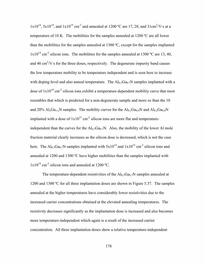
178
1x10¹⁴, 5x10¹⁴, and 1x1015 cm-2 and annealed at 1200 ºC are 17, 28, and 31cm2/V·s at a
temperature of 10 K. The mobilities for the samples annealed at 1200 ºC are all lower
than the mobilities for the samples annealed at 1300 ºC, except for the samples implanted
1x1014 cm-2 silicon ions. The mobilities for the samples annealed at 1300 ºC are 13, 40,
and 46 cm2/V·s for the three doses, respectively. The degenerate impurity band causes
the low temperature mobility to be temperature independent and is seen here to increase
with doping level and also anneal temperature. The Al0.3Ga0.7N samples implanted with a
dose of 1x1014 cm-2 silicon ions exhibit a temperature-dependent mobility curve that most
resembles that which is predicted for a non-degenerate sample and more so than the 10
and 20% AlxGa1-xN samples. The mobility curves for the Al0.1Ga0.9N and Al0.2Ga0.8N
implanted with a dose of 1x1015 cm-2 silicon ions are more flat and temperature-
independent than the curves for the Al0.3Ga0.7N. Also, the mobility of the lower Al mole
fraction material clearly increases as the silicon dose is decreased, which is not the case
here. The Al0.3Ga0.7N samples implanted with 5x10¹⁴ and 1x1015 cm-2 silicon ions and
annealed at 1200 and 1300 ºC have higher mobilities than the samples implanted with
1x1014 cm-2 silicon ions and annealed at 1200 ºC.
The temperature-dependent resistivities of the Al0.3Ga0.7N samples annealed at
1200 and 1300 ºC for all three implantation doses are shown in Figure 5.37. The samples
annealed at the higher temperatures have considerably lower resistivities due to the
increased carrier concentrations obtained at the elevated annealing temperatures. The
resistivity decreases significantly as the implantation dose is increased and also becomes
more temperature-independent which again is a result of the increased carrier
concentration. All three implantation doses show a relative temperature-independent

0 20 40 60 80 1000
100
200
300
400
500
600
2000
3000
4000
5000
6000
7000
Temperature (K)
1000/T (K-1)
Al0.3Ga0.7N:SitA = 20 minutes
Sh
eet R
esis
tivity
(Ω/s
q.) 1x1015 cm-2
1200 oC 1300 oC5x1014 cm-2
1200 oC 1300 oC1x1014 cm-2
1200 oC 1300 oC
800 100 50 25 20 15 10
Figure.5.37. Temperature-dependent resistivity values calculated from Hall measurements taken from 10 to 700 K for Al0.3Ga0.7N that had been implanted at room temperature with silicon ions at 200 keV with doses of 1x10¹⁴, 5x10¹⁴, and 1x1015 cm-2 and annealed at 1200 and 1300ºC for 20 minutes in flowing nitrogen.
179

180
resistivity from 10 to 50 K before the resistivity slowly begins to decline to a minimum
around 240-380 K at which point the resistivity begins to increase as the samples
temperature is raised to 700 K. The dip in the resistivity curve for the samples implanted
with 1x1014 cm-2 silicon ions is the most exaggerated while, the drop in the resistivity of
the samples implanted with a silicon dose of 1x1015 cm-2 is almost unnoticeable. The
decline in the resistivity curves around 300 K are a result of the rapid increase in the
carrier concentration as the sample temperature is increased. The resistivity begins to
increase at higher temperatures due to the decrease in the mobility as ionized impurity
scattering becomes dominant. The resistivities curves for the Al0.3Ga0.7N are similar is
shape and value to those of the Al0.1Ga0.9N and Al0.2Ga0.8N. In all three cases, the
samples annealed at 1300 ºC have lower resistivities than the samples annealed at 1200
ºC. The implanted silicon dose has the most profound effect on the resistivity of the
samples. Increasing the implanted silicon dose causes the resistivity of the material to
decrease significantly and also causes the resistivity to become more temperature-
independent.
Low Temperature Cathodoluminescence Measurements
Cathodoluminescence measurements were taken with an electron energy of 10
keV with 50 µA of source current, the temperature in the chamber was 7.4 K, and the
slits on the spectrometer were 400 µm both at the entrance and the exit. The range
scanned was 1800 to 7000 Å with a step size of 2 Å with an integration time of 0.1
second.
The spectrum of the unimplanted samples shown as a function of anneal
temperature are given in Figure 5.38. To gauge the effects of the annealing on the

2 3 4 5 6
3.99 eV3.90 eV
3.8 eV
Wavelength (nm)
1250 oC
1300 oC
1150 oCx1/2
x1/2
4.08 eV
x1/2
1200 oC
Unimplanted Al0.3Ga0.7NT=7.4 K
C
L In
tens
ity (a
rb. u
nits
)
Energy (eV)
As-grown
700 500 400 300 200
Figure 5.38.CL spectra taken at 7.4 K for unimplanted Al0.3Ga0.7N that have been anneal at 1150, 1200, 1250 and 1350 ºC for 20 minutes in flowing nitrogen and also an as-grown sample.
181

182
implanted samples, the behavior of the unimplanted samples must first be analyzed. The
CL spectra for all the unimplanted samples all show a good neutral-donor-bound exciton
(Do,X) peak at 4.08 eV, except for the sample annealed at 1250 ºC. Nepal et al. identify a
dominant peak at 4.27 eV in un-doped Al0.38Ga0.62N which they attribute to localized
exciton transitions (61). The spectra for the as-grown sample and the samples annealed
at 1150 and 1200 ºC have been reduced by a factor of 2, to enhance the features of the
spectra for the samples annealed at 1250 and 1300 ºC. The spectrum for the as-grown
sample also has two small peaks at 3.99 and 3.90 eV which can be attributed to etalon
effects. At first, the intensity of the (Do,X) peak increases as the anneal temperature is
increased up to 1200 ºC. The samples annealed at 1150 and 1200 ºC have CL spectra that
closely resemble that of the as-grown sample in both intensity and sharpness. Further
increasing the anneal temperature to 1250 ºC causes the (Do,X) peak intensity to weaken
considerably and a broad extension at 3.8 eV, most likely caused by defects created
during the high temperature anneal. This broad emission centered around 3.8 eV is only
evident in the sample annealed at 1250 ºC. Increasing the anneal temperature up to 1300
ºC recovers the (Do,X) peak however, it still has a much weaker intensity than the as-
grown sample. The unimplanted Al0.3Ga0.7N respond better to low temperature annealing
rather than high temperature annealing, indicating some annealing damage may occur for
this Al mole fraction after annealing at 1250 ºC or higher.
The low temperature CL spectra for the Si-implanted Al0.3Ga0.7N annealed for 20
minutes at 1300 ºC are shown in Figure 5.39. All of the spectra show a (Do,X) peak at
4.08 eV, with a slight broadening toward lower energies. The implanted samples all
exhibit a more intense (Do,X) peak than that of the unimplanted sample, however the
unimplanted sample’s spectrum annealed at this temperature is highly reduced from that

2 3 4 5 6
Wavelength (nm)
4.08 eV
Si-implanted Al0.3Ga0.7N
Anneal: 1300oC/ 20 min.T=7.4 K
C
L In
tens
ity (a
rb. u
nits
)
Energy (eV)
1x1014 cm-2
Unimplanted, annealed
5x1014 cm-2
1x1015 cm-2
700 500 400 300 200
Figure 5.39. CL spectra taken at 7.4 K for Al0.3Ga0.7N that have been anneal at 1300 ºC for 20 minutes in flowing nitrogen.
183

184
of the as-grown sample. The intensity of the (Do,X) peak does not increase as the
implanted silicon is decreased as it had in the previous Al mole fraction material. The
Al0.3Ga0.7N samples implanted with a silicon dose of 5x1014 cm-2 have a lower intensity
than the samples implanted with the other silicon dose. The spectra of the Al0.3Ga0.7N,
like those of the Al0.2Ga0.8N, do not show the broad yellow band (YL) that was seen in
the spectra of the Al0.1Ga0.9N. The (Do,X) peak broadens towards lower energy as the
implanted silicon dose is increased from 1x10¹⁴ to 1x1015 cm-2.
The near band edge broadening on the low energy side of the (Do,X) peak, seen
primarily in the spectra for the sample implanted with 1x1015 cm-2 silicon ions, is due
mainly to band tailing effects. The implanted silicon doses exceed the Mott
concentration of Al0.3Ga0.7N, which can result in band-edge effects such as band filling
and band tailing. Band filling, seen in the CL spectrum as broadening of the (Do,X) peak
towards higher energies, occurs in highly-doped semiconductors when the Fermi energy
moves toward very close to the conduction band or into the conduction band, thus
allowing for transitions to occur at higher energies than the band gap. Only the sample
implanted with a silicon dose of 1x1015 cm-2 has a volume carrier concentration high
enough for noticeable band filling to occur.
The low temperature CL spectra for the Al0.3Ga0.7N implanted with 1x1014 cm-2
silicon ions and annealed for 20 minutes at various temperatures are shown in Figure
5.40. All of the anneal temperatures produce spectra with a good (Do,X) peak centered at
4.08 eV, except for the sample that was annealed at 1200 ºC. The peak for this sample
has shifter to 4.0 eV. The spectra for the as-grown sample and the sample annealed at
1150 ºC had to be reduced 150th of their original size. The samples annealed at 1250 and

2 3 4 5 6
Wavelength (nm)
2.61 eV
4.00 eV
4.08 eV
x 1/15
x 1/150
x 1/150
Si-implanted Al0.3Ga0.7N
1x1014cm-2
T=7.4 K
1300 oC
1250 oC
1150 oC
1200 oC
As-grown
x 1/100
C
L In
tens
ity (a
rb. u
nits
)
Energy (eV)
700 500 400 300 200
Figure 5.40. CL spectra taken at 7.4 K for Al0.3Ga0.7N that has been implanted with 1x1014 cm-2 silicon ions and annealed at various temperatures for 20 minutes in flowing nitrogen.
185

186
1300 ºC also had to be reduced, but only by a factor of 15 and 100, respectively. Like the
unimplanted Al0.3Ga0.7N, these samples exhibit their most intense (Do,X) peak following
the 1150 ºC. The intensity of the (Do,X) peak for this temperature is only slightly less
than that of the as-grown sample. Increasing the anneal temperature to 1200 ºC has
detrimental effects on the spectra, the intensity of the (Do,X) peak decreases and a broad
luminescence, similar to the YL band seen in the Al0.1Ga0.9N, emerges. The intensity of
the (Do,X) peak and the intensity with the broad band luminescence centered at 2.61 eV
are almost equal. The CL spectra improve considerably as the anneal temperature is
raised to 1300 ºC. The sample annealed at 1250 ºC exhibits the YL band that has a much
reduced intensity from that of the sample that was annealed at 1200 ºC. The 2.61 eV
band is most likely related to implanted related defects, such as transitions from a silicon
donor to an aluminum vacancy, that are activated at higher anneal temperatures. The
spectra for the sample annealed at 1250 ºC also has a large broad shoulder off the low
energy side of the (Do,X) peak that is similar to the broad emission in the spectra for the
unimplanted sample annealed at this temperature. The unimplanted sample annealed at
1250 ºC has a broad luminescence centered at 3.7 eV that could be related to damage
caused during the anneal. Further increasing the anneal temperature to 1300 ºC produces
a spectra with a sharp (Do,X) peak and no YL band, similar to the spectrum of the
unimplanted sample. The intensity of the (Do,X) peak for the Al0.3Ga0.7N samples
implanted with a silicon dose of 1x1014 cm-2 increases as the anneal temperature is
increased from 1200 to 1300 ºC, signifying successive improvement in the crystal lattice
with each increase in the anneal temperature. The spectrum of the sample annealed at
1150 ºC has the best recovery of the (Do,X) peak however, this sample has the lowest
activation efficiency. An anneal temperature of 1200 ºC produced significantly reduced
187
intensity with no apparent reason, however the carrier concentration for this sample
increased 73% over that of the sample annealed at 1150 ºC. An anneal temperature of
1300 ºC produced an excellent peak signifying that the majority of the implantation
induced damage had been restored and most of the silicon ions have been activated. The
increase in intensity of the (Do,X) peaks observed for the anneal temperatures of 1200,
1250, and 1300 ºC indicate that more of the implanted silicon ions have become
electrically active as the anneal temperature was increased. The CL spectra agree very
well with the electrical activation results obtained from Hall Effect measurements for the
Al0.3Ga0.7N implanted with this silicon dose. The sharpness and strong intensity of the
peak for the sample annealed at 1300 ºC correlate well with the high activation and
mobility values obtained on this sample. The (Do,X) peak and the high mobilities
observed on the these samples indicate excellent implantation damage recovery after
annealing at 1300 ºC for 20 minutes in flowing nitrogen.
Figure 5.41 shows the CL spectra of the Al0.3Ga0.7N implanted with a silicon dose
of 5x1014 cm-2 and annealed for 20 minutes at various temperatures. All the spectrum
have a (Do,X) peak at 4.08 eV with a small shoulder on the low energy side. The sample
annealed at 1150 ºC produces a good (Do,X) peak that is only slightly more intense peak
than the samples annealed at 1200 and 1300 ºC. The intensity of the spectrum of the
sample annealed at 1200 ºC is much reduced, like the Al0.3Ga0.7N samples implanted with
a silicon dose of 1x1014 cm-2, for unknown reasons. The samples implanted with 5x10¹⁴
cm-2 silicon ions exhibit their strongest (Do,X) peak after being annealed at 1250 ºC for
20 minutes, which is more intense than the as-grown sample. However, the sample
annealed at 1300 ºC for 20 minutes again shows a diminished intensity for unknown
reasons. The spectrum of the sample annealed at 1350 ºC closely resembles that of the
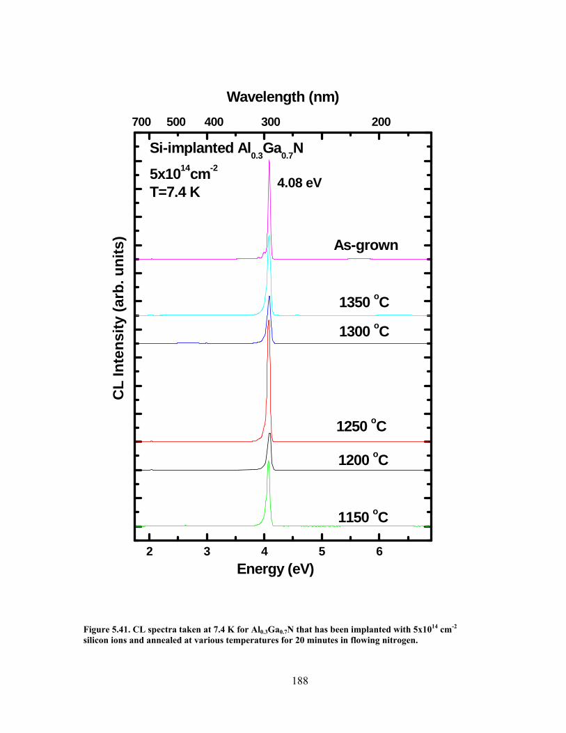
2 3 4 5 6
Wavelength (nm)
1350 oC
Si-implanted Al0.3Ga0.7N
5x1014cm-2
T=7.4 K
1200 oC
1250 oC
1300 oC
1150 oC
As-grown
4.08 eV
C
L In
tens
ity (a
rb. u
nits
)
Energy (eV)
700 500 400 300 200
Figure 5.41. CL spectra taken at 7.4 K for Al0.3Ga0.7N that has been implanted with 5x1014 cm-2 silicon ions and annealed at various temperatures for 20 minutes in flowing nitrogen.
188

189
as-grown sample in both intensity and sharpness. The Al0.2Ga0.8N samples implanted
with this dose also display their best (Do,X) peak at lower anneal temperatures. The
intensity of the (Do,X) peak swamps out the broad band luminescence centered at 2.61
eV, that is present in the samples annealed at 1250, 1300 and 1350 ºC. This
luminescence becomes more intense as the anneal temperature is increased. The samples
annealed at lower temperatures do not have any broad band luminescence. The
Al0.3Ga0.7N samples implanted with 1x1014 cm-2 silicon ions and annealed at 1200 and
1250 ºC also exhibit this luminescence only it decreases ad the anneal temperature is
increased and is not present in the spectrum of the sample annealed at 1300 ºC.
The CL spectra of the samples implanted with the highest silicon dose of 1x10¹⁵
cm-2 and annealed for 20 minutes at various temperatures are shown in Figure 5.42. The
CL spectra exhibit the same dependence on the anneal temperature as the samples
implanted 5x1014 cm-2 silicon ions. All the spectra have a (Do,X) peak at 4.08 eV that
slightly broadens on the lower energy side. The (Do,X) peak for the sample annealed at
1250 ºC has the strongest intensity, which is stronger than the as-grown sample, however
it has broadened both toward high and low energies due to band filling and band tailing
effects. The samples annealed at 1150 and 1300 ºC have about the same intensity
however, the sample annealed at 1300 ºC has a much broader peak due to the enhance
effects of band tailing. The intensity of the peak increases as does the full width half max
of the peak upon extending the anneal temperature from 1150 to 1250 ºC. The spectrum
of the sample annealed at 1200 ºC has been increased 100 times of its original size. This
spectrum shows a broad and weak peak centered at 4.0 eV and broad band centered at
2.61 eV, similar to the spectrum of the Al0.3Ga0.7N sample implanted with 1x1014 cm-2
silicon ions and annealed at this temperature. The spectrum for the samples annealed at

2 3 4 5 6
Wavelength (nm)
x 1002.61 eV
4.08 eV
4.00 eV
1200 oC
1250 oC
1300 oC
1150 oC
As-grown
Si-implanted Al0.3Ga0.7N
1x1015cm-2
T=7.4 K
C
L In
tens
ity (a
rb. u
nits
)
Energy (eV)
700 500 400 300 200
Figure 5.42. CL spectra taken at 7.4 K for Al0.3Ga0.7N that has been implanted with 1x1015 cm-2 silicon ions and annealed at various temperatures for 20 minutes in flowing nitrogen.
190
191
1250 and 1300 ºC also exhibit a broad luminescence at 2.61 eV that has a much reduced
intensity than the (Do,X) peaks for these spectra and are not visible. This broad band
luminescence decreases as the anneal temperature is increased.
The spectra for the Al0.3Ga0.7N samples that were implanted with all three doses and
annealed at 1200 ºC all experience a significant decrease in intensity for no obvious
reason. As the anneal temperature was increased, this was the lowest anneal temperature
to produce the 2.61 eV band for the samples implanted with 1x10¹⁴ and 1x1015 cm-2
silicon ions, which also corresponds to the temperature that the carrier concentration
experiences its largest increase. This band has been suggested to be related to a silicon
donor and a deep acceptor (44). The 2.61 eV band does not emerge for the samples
implanted with 5x1014 cm-2 silicon ions until they were annealed at 1250 ºC. These
samples experience the diminished intensity of the sample annealed at 1200 ºC and also
again for the samples annealed at 1300 ºC, which corresponds to the temperatures that he
carrier concentration increases the most. This could be considered the temperature
required to excite the lattice enough for incorporation of the silicon ions to take place.
Silicon Implanted Al0.4Ga0.6N
Electrical and optical properties of Si-implanted AlxGa1-xN with Al concentrations
of 40 and 50% have not been reported in the literature. However, there is literature that
addresses the effects of silicon doping on high Al mole fraction (x >0.5) AlxGa1-xN.
Hwang et al. investigated the effects of silicon doping on Al0.65Ga0.35N that had a room
temperature carrier concentration of 8.0x1019 cm-3 and mobility of 18 cm2/V·s (51).
Temperature-dependent Hall measurements on this sample exhibited no change with the
increasing temperature, indicating the sample was degenerate. Nakarmi et al.
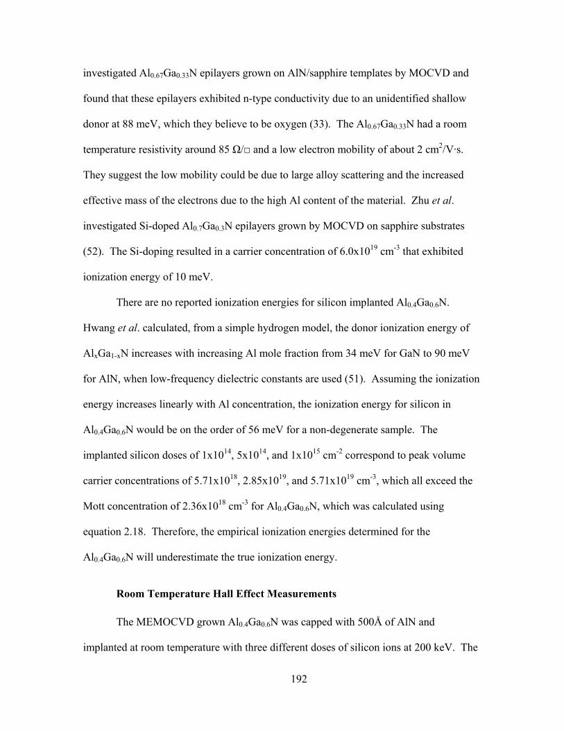
192
investigated Al0.67Ga0.33N epilayers grown on AlN/sapphire templates by MOCVD and
found that these epilayers exhibited n-type conductivity due to an unidentified shallow
donor at 88 meV, which they believe to be oxygen (33). The Al0.67Ga0.33N had a room
temperature resistivity around 85 Ω/ and a low electron mobility of about 2 cm2/V·s.
They suggest the low mobility could be due to large alloy scattering and the increased
effective mass of the electrons due to the high Al content of the material. Zhu et al.
investigated Si-doped Al0.7Ga0.3N epilayers grown by MOCVD on sapphire substrates
(52). The Si-doping resulted in a carrier concentration of 6.0x1019 cm-3 that exhibited
ionization energy of 10 meV.
There are no reported ionization energies for silicon implanted Al0.4Ga0.6N.
Hwang et al. calculated, from a simple hydrogen model, the donor ionization energy of
AlxGa1-xN increases with increasing Al mole fraction from 34 meV for GaN to 90 meV
for AlN, when low-frequency dielectric constants are used (51). Assuming the ionization
energy increases linearly with Al concentration, the ionization energy for silicon in
Al0.4Ga0.6N would be on the order of 56 meV for a non-degenerate sample. The
implanted silicon doses of 1x10¹⁴, 5x10¹⁴, and 1x1015 cm-2 correspond to peak volume
carrier concentrations of 5.71x10¹⁸, 2.85x10¹⁹, and 5.71x1019 cm-3, which all exceed the
Mott concentration of 2.36x1018 cm-3 for Al0.4Ga0.6N, which was calculated using
equation 2.18. Therefore, the empirical ionization energies determined for the
Al0.4Ga0.6N will underestimate the true ionization energy.
Room Temperature Hall Effect Measurements
The MEMOCVD grown Al0.4Ga0.6N was capped with 500Å of AlN and
implanted at room temperature with three different doses of silicon ions at 200 keV. The
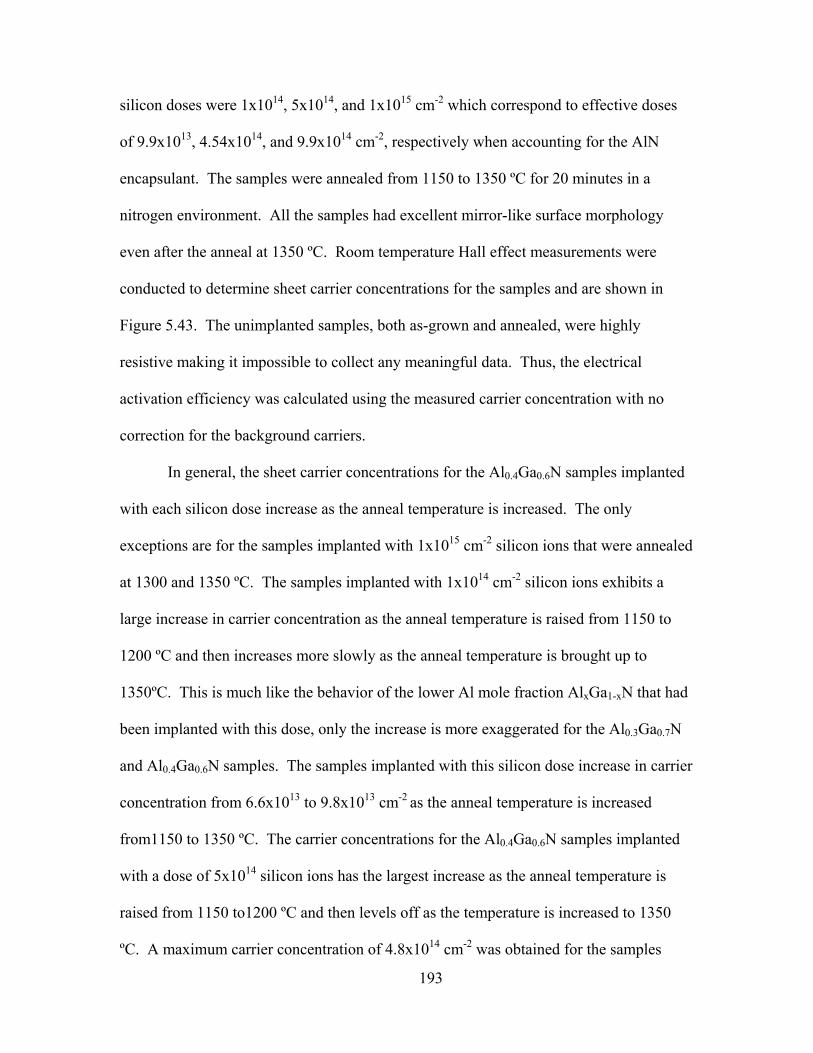
193
silicon doses were 1x10¹⁴, 5x10¹⁴, and 1x1015 cm-2 which correspond to effective doses
of 9.9x10¹³, 4.54x10¹⁴, and 9.9x1014 cm-2, respectively when accounting for the AlN
encapsulant. The samples were annealed from 1150 to 1350 ºC for 20 minutes in a
nitrogen environment. All the samples had excellent mirror-like surface morphology
even after the anneal at 1350 ºC. Room temperature Hall effect measurements were
conducted to determine sheet carrier concentrations for the samples and are shown in
Figure 5.43. The unimplanted samples, both as-grown and annealed, were highly
resistive making it impossible to collect any meaningful data. Thus, the electrical
activation efficiency was calculated using the measured carrier concentration with no
correction for the background carriers.
In general, the sheet carrier concentrations for the Al0.4Ga0.6N samples implanted
with each silicon dose increase as the anneal temperature is increased. The only
exceptions are for the samples implanted with 1x1015 cm-2 silicon ions that were annealed
at 1300 and 1350 ºC. The samples implanted with 1x1014 cm-2 silicon ions exhibits a
large increase in carrier concentration as the anneal temperature is raised from 1150 to
1200 ºC and then increases more slowly as the anneal temperature is brought up to
1350ºC. This is much like the behavior of the lower Al mole fraction AlxGa1-xN that had
been implanted with this dose, only the increase is more exaggerated for the Al0.3Ga0.7N
and Al0.4Ga0.6N samples. The samples implanted with this silicon dose increase in carrier
concentration from 6.6x10¹³ to 9.8x1013 cm-2 as the anneal temperature is increased
from1150 to 1350 ºC. The carrier concentrations for the Al0.4Ga0.6N samples implanted
with a dose of 5x10¹⁴ silicon ions has the largest increase as the anneal temperature is
raised from 1150 to1200 ºC and then levels off as the temperature is increased to 1350
ºC. A maximum carrier concentration of 4.8x1014 cm-2 was obtained for the samples

1150 1200 1250 1300 1350
1013
1014
1015
Al0.4Ga0.6N:Si
1x1014 cm-2
5x1014 cm-2
1x1015 cm-2
o
Sh
eet C
arrie
r Con
cent
ratio
n (c
m-2)
Figure 5.43. Room temperature sheet carrier concentrations for Al0.4Ga0.6N implanted at room temperature with silicon ions at 200 keV with doses of 1x10¹⁴, 5x10¹⁴, and 1x1015 cm-2 and annealed from 1150 to 1350 ºC for 20 minutes in flowing nitrogen.
194
195
implanted with a silicon dose of 5x1014 cm-2 following a 20 minute anneal at 1350 ºC.
The carrier concentrations for the Al0.4Ga0.6N implanted with a dose of 1x1015 cm-2
silicon ions increases as the temperature is raised from 1150 to 1250 ºC and then shows a
slight decline as the anneal temperature is further increased to 1350 ºC. The Al0.4Ga0.6N
implanted with a silicon dose of 1x1015 cm-2 reaches a maximum carrier concentration of
9.55x1014 cm-2 after being annealed for 20 minutes at 1250 ºC. The Al0.1Ga0.9N samples
implanted with the highest silicon dose also had a decline in the carrier concentration
after being annealed at higher temperatures of 1200 and 1250 ºC.
Figure 5.44 shows the electrical activation for the Al0.4Ga0.6N that was
calculated using the effective doses and room temperature sheet carrier concentrations.
The silicon electrical activation of these samples is closely related to the carrier
concentration and follows the same trends with the anneal temperature as mentioned
above. The Al0.4Ga0.6N implanted with all three silicon doses exhibit excellent activation
above 90% after the high temperature anneal. The samples implanted with 1x1014 cm-2
silicon ions have activation efficiencies that increase as the anneal temperatures are
increased up to 1350 ºC. The activation of the Al0.4Ga0.6N implanted with 5x1014 cm-2
silicon ions increases rapidly as the anneal temperature is raised from 1150 to 1250 ºC
and then steadies off and slowly increases as the anneal temperature is raised to 1350 ºC.
The electrical activation for the samples implanted with 1x1015 cm-2 silicon ions peaks
for the sample annealed at 1250 ºC and then begins to decline for the samples that were
annealed at higher temperatures. The decrease in activation efficiency could be due to
out diffusion of silicon or compensating acceptor-like defects that were created during the
higher temperature anneals. However, the activation of the Al0.4Ga0.6N implanted with
this silicon dose still has a significant activation of 78% after being annealed at 1350 ºC.

1150 1200 1250 1300 1350
0
10
20
30
40
50
60
70
80
90
100
110
Al0.4Ga0.6N:Si
1x1014 cm-2
5x1014 cm-2
1x1015 cm-2
Anneal Temperature (oC)
Silic
on E
lect
rical
Act
ivat
ion
Effic
ienc
y (%
)
Figure 5.44. Silicon electrical activation efficiency for Al0.4Ga0.6N calculated from the room temperature Hall measurements for Si-implanted doses of 1x10¹⁴, 5x10¹⁴, and 1x1015 cm-2 and annealed from 1150 to 1350 ºC for 20 minutes.
196

197
This activation is higher than that for the samples implanted with this silicon dose and
annealed at 1150 ºC which is of 67 %.
The samples implanted with 1x1014 cm-2 silicon ions exhibit the most
improvement over the given temperature range, increasing from 6% to 99% after being
annealed for 20 minutes at 1150 ºC and 1350 ºC, respectively. The Al0.4Ga0.6N
implanted with this silicon dose had the lowest activations but showed the
best response to an increase in the anneal temperature, indicating that a further increase in
the anneal temperature or time may result in higher activation. This behavior is
consistent with the AlxGa1-xN samples with Al concentrations from 10 to 30% that were
implanted with this silicon dose. The activation efficiencies of the Al0.4Ga0.6N implanted
with a dose of 5x1014 cm-2 silicon ions reach a peak activation of 97%, for the sample that
was annealed at 1350 ºC for 20 minutes. The peak activation efficiency for the
Al0.2Ga0.8N implanted with this dose was 100% after being annealed at 1300 ºC for 20
minutes. The Al0.1Ga0.9N and Al0.3Ga0.7N samples implanted with this silicon dose
achieved lower peak activations for various annealing conditions. The maximum
activation for the Al0.1Ga0.9N samples implanted with 5x1014 cm-2 silicon ions was 94%
after a 40 minute anneal at 1200 ºC, while the activation for the Al0.3Ga0.7N was
considerably lower at 88% for the sample annealed at 1300 ºC for 20 minutes. The
Al0.4Ga0.6N implanted with the highest silicon dose of 1x1015 cm-2 reaches 96%
activation after being annealed at 1250 ºC for 20 minutes in a nitrogen ambient. The
activation efficiencies of the AlxGa1-xN, with Al concentrations from 10 to 30%,
implanted with the same silicon dose all reach 100% after being annealed at
various temperatures. All of the implanted silicon doses are readily activated in
Al0.4Ga0.6N, which is illustrated in Figure 5.45. Considerably lower anneal temperatures

1E14 1E15
1E13
1E14
1E15
Actual Implanted Si Dose (cm-2)
Shee
t car
rier C
oncn
etra
tion
(cm
-2)
Al0.4Ga0.6N:Si
1150oC/20min. 1200oC/20min. 1250oC/20min. 1300oC/20min. 1350oC/20min.
100% Activation
Figure 5.45. The room temperature sheet carrier concentrations versus the actual implantation dose for Al0.4Ga0.6N implanted at room temperature with silicon ions at 200 keV with doses of 1x10¹⁴, 5x10¹⁴, and 1x1015 cm-2 and annealed from 1150 ºC to 1350 ºC for 20 minutes in a nitrogen ambient.
198

199
were required to achieve a high activation efficiency in the samples implanted with
1x1015 cm-2 silicon ions than in the samples implanted with the lower silicon doses. The
Al0.4Ga0.6N is the only material to have an activation efficiency above 85% for the
samples implanted with a dose of 1x1014 cm-2 silicon ions.
The optimal annealing temperature based solely on the results of activation
efficiency is found to be dose dependant in the Al0.4Ga0.6N, as it was for the AlxGa1-xN
with lower Al mole fractions. The lower the implanted silicon dose the higher the
annealing temperature required to achieve high electrical activation. The samples
implanted with the lower silicon doses of 1x10¹⁴ and 5x1014 cm-2 have an optimal anneal
temperature of 1350, while the optimal anneal temperature for the samples implanted
with 1x1015 cm-2 silicon ions is 1250 ºC.
The resistivities of the Si-implanted Al0.4Ga0.6N implanted with each silicon dose
and annealed for 20 minutes at various temperatures are shown in Figure 5.46. The
samples implanted with 1x1014 cm-2 silicon ions exhibit the largest measured resistivity
181 kΩ/, which is 118 and 487 times higher than the samples implanted with 5x10¹⁴ and
1x1015 cm-2 silicon ions when annealed at 1150 ºC for 20 minutes. The resistivity for
these samples falls about 180 kΩ/ as the anneal temperature is increased to 1350 ºC. As
seen in the AlxGa1-xN with lower Al mole fractions the resistivity of all the samples
decreases as the anneal temperature is increased due to the increase in the carrier
concentration and mobility as the temperature is increased. The Al0.4Ga0.6N implanted
with 5x1014 cm-2 silicon ions show a rapid decrease in resistivity as the anneal
temperature is increased from 1150 to 1200 ºC and then decreases linearly as the anneal
temperature is raised to 1350 ºC. The resistivity for the samples implanted with this dose
drops from 1.5 kΩ/ to 213 Ω/ after being annealed at 1150 and 1350 ºC. The

1150 1200 1250 1300 13500
500
1000
1500
2000
2500
3000
3500
160000
180000
200000
Al0.4Ga0.6N:Si
1x1014 cm-2
5x1014 cm-2
1x1015 cm-2
tA= 20 min
Anneal Temperature (oC)
Res
istiv
ity (Ω
/sq.
)
Figure 5.46. Room temperature resistivity measurements taken under zero magnetic field for Al0.4Ga0.6N implanted at room temperature with silicon ions at 200 keV with doses of 1x10¹⁴, 5x10¹⁴, and 1x1015 cm-2 and annealed from 1150 ºC to 1350 ºC for 20 minutes in a nitrogen ambient.
200
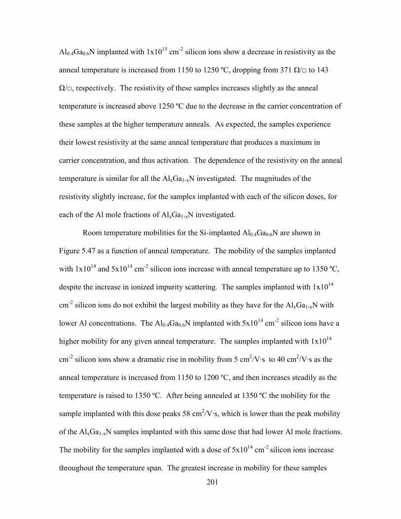
201
Al0.4Ga0.6N implanted with 1x1015 cm-2 silicon ions show a decrease in resistivity as the
anneal temperature is increased from 1150 to 1250 ºC, dropping from 371 Ω/ to 143
Ω/, respectively. The resistivity of these samples increases slightly as the anneal
temperature is increased above 1250 ºC due to the decrease in the carrier concentration of
these samples at the higher temperature anneals. As expected, the samples experience
their lowest resistivity at the same anneal temperature that produces a maximum in
carrier concentration, and thus activation. The dependence of the resistivity on the anneal
temperature is similar for all the AlxGa1-xN investigated. The magnitudes of the
resistivity slightly increase, for the samples implanted with each of the silicon doses, for
each of the Al mole fractions of AlxGa1-xN investigated.
Room temperature mobilities for the Si-implanted Al0.4Ga0.6N are shown in
Figure 5.47 as a function of anneal temperature. The mobility of the samples implanted
with 1x10¹⁴ and 5x1014 cm-2 silicon ions increase with anneal temperature up to 1350 ºC,
despite the increase in ionized impurity scattering. The samples implanted with 1x10¹⁴
cm-2 silicon ions do not exhibit the largest mobility as they have for the AlxGa1-xN with
lower Al concentrations. The Al0.4Ga0.6N implanted with 5x1014 cm-2 silicon ions have a
higher mobility for any given anneal temperature. The samples implanted with 1x10¹⁴
cm-2 silicon ions show a dramatic rise in mobility from 5 cm2/V·s to 40 cm2/V·s as the
anneal temperature is increased from 1150 to 1200 ºC, and then increases steadily as the
temperature is raised to 1350 ºC. After being annealed at 1350 ºC the mobility for the
sample implanted with this dose peaks 58 cm2/V·s, which is lower than the peak mobility
of the AlxGa1-xN samples implanted with this same dose that had lower Al mole fractions.
The mobility for the samples implanted with a dose of 5x1014 cm-2 silicon ions increase
throughout the temperature span. The greatest increase in mobility for these samples
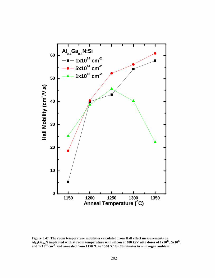
1150 1200 1250 1300 13500
10
20
30
40
50
60
Anneal Temperature (oC)
Hal
l Mob
ility
(cm
2 /V.s
)Al0.4Ga0.6N:Si
1x1014 cm-2
5x1014 cm-2
1x1015 cm-2
Figure 5.47. The room temperature mobilities calculated from Hall effect measurements on Al0.4Ga0.6N implanted with at room temperature with silicon at 200 keV with doses of 1x10¹⁴, 5x10¹⁴, and 1x1015 cm-2 and annealed from 1150 ºC to 1350 ºC for 20 minutes in a nitrogen ambient.
202

203
occurs for the samples annealed from 1150 to 1250 ºC. The Al0.4Ga0.6N implanted with
this dose reaches a peak mobility of 61 cm2/V·s after being annealed for 20 minutes at
1350 ºC, which is only slightly less than the Al0.3Ga0.7N sample implanted with the same
dose and annealed under the same conditions. The mobility of the samples implanted
with 1x1015 cm-2 silicon ions increase linearly as the temperature is raised from 1150 to
1250 ºC reaching a peak mobility of 45 cm2/V·s. A further increase in the anneal
temperature causes a decline in the mobility and activation for these samples, therfore the
decrease in the mobility is not due to an increase in ionized impurity scattering. The
decrease in the mobility can most likely be attributed to an increase in defect scattering
due to damage caused from the high temperatures of the anneal. The mobilities for the
Al0.1Ga0.9N, Al0.2Ga0.8N and Al0.3Ga0.7N samples implanted with the same dose are all
higher at 90, 76 and 61 cm2/V·s, respectively. The magnitude of the mobility for the
Al0.4Ga0.6N is not as large as it was for the AlxGa1-xN with lower Al mole fractions which
could be due to an increase in the effective mass as the Al mole fraction is increased (33).
The mobility of the Al0.4Ga0.6N implanted with the lower two silicon doses
increases as the anneal temperature is increased despite the increased effects of ionized
impurity scattering, indicating that lattice damage is still being repaired even at anneal
temperatures up to 1350 ºC. The samples implanted with the highest silicon dose exhibit
an increase in the mobility with activation for annealing temperatures up to 1250 ºC,
however they both decline as the anneal temperature is increased, thus indicating that
before the lattice damage could be repaired annealing damage became a dominating
factor. This is the first time this behavior has been seen.
To improve the electrical activation efficiency of the implanted silicon in the Al0.4Ga0.6N
the anneal time was extended from 20 to 40 minutes for a set anneal temperature of 1200

204
ºC. A comparison of the results obtained for both the 20 and 40 minute anneals at 1200
ºC are listed in Table 5.3. Extending the anneal time had positive affects on all of the
physical aspects determined from Hall effect measurements. The carrier concentrations
and therefore activation energy of the all the implanted samples increased following the
40 minute anneal. The resistivity of all the implanted samples decreases as does the
mobility, except for the Al0.4Ga0.6N implanted with 5x1014 cm-2 silicon ions, which show
a slight decease in mobility after being annealed for 40 minutes. The samples implanted
with 1x1014 cm-2 silicon ions exhibit a significant 20% increase in the electrical activation
efficiency going from 45 to 66% after the 20 and 40 minute anneals, respectively. The
resistivity drops 40% to 2142 Ω/ for the samples implanted with the lowest silicon dose
after being annealed for 40 minutes at 1200 ºC. The mobility for these samples increases
slightly from 40.0 cm2/V·s to 44.5 cm2/V·s, despite an increase in ionized impurity
scattering. The samples implanted with 5x1014 cm-2 silicon ions exhibit a 20% increase
in the electrical activation bringing it up to 100% following the 40 minute anneal. The
resistivity of these samples decreases 22% to 316 Ω/. The Al0.4Ga0.6N implanted with
this dose were the only samples to show a decrease in mobility due to an increase in
ionized impurity scattering when the anneal time was extended to 40 minutes. The
mobility for the samples implanted with 5x1014 cm-2 silicon ions decreases only slightly
from 40.5 to 37.9 cm2/V·s. The Al0.4Ga0.6N implanted with a dose of 1x1015 cm-2 silicon
ions have an activation of 96% following a 20 minute anneal at 1200 ºC, extending the
anneal time to 40 minutes resulted in an insignificant increase in the activation of 0.4%.
The resistivity for these samples decreases about 6 %, which is less than 10 Ω/. The
mobility for the samples implanted with the highest silicon dose had a negligible increase
from 38.7 to 41.1 cm2/V·s after extending the anneal time to 40 minutes.
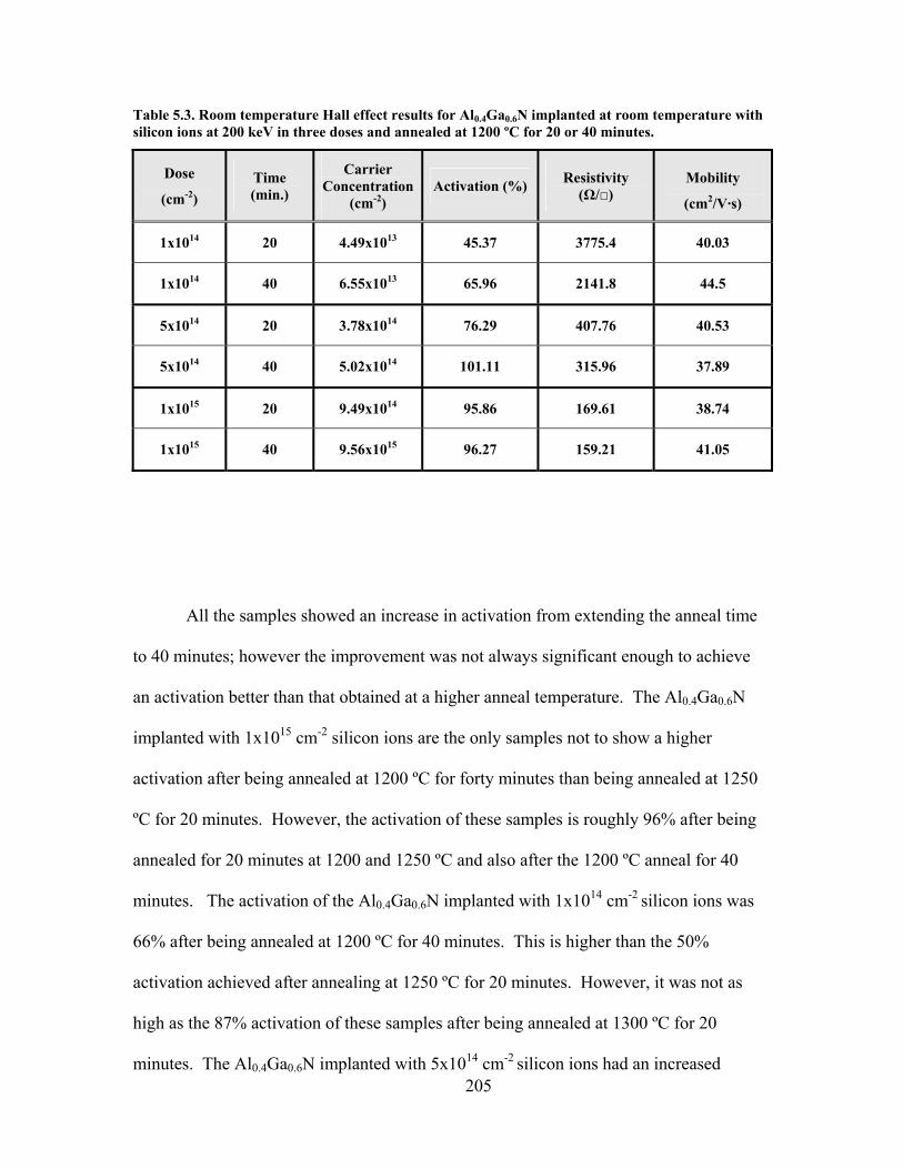
205
Table 5.3. Room temperature Hall effect results for Al0.4Ga0.6N implanted at room temperature with silicon ions at 200 keV in three doses and annealed at 1200 ºC for 20 or 40 minutes.
Dose
(cm-2) Time (min.)
Carrier Concentration
(cm-2) Activation (%) Resistivity
(Ω/) Mobility
(cm2/V·s)
1x10¹⁴ 20 4.49x10¹³ 45.37 3775.4 40.03
1x10¹⁴ 40 6.55x10¹³ 65.96 2141.8 44.5
5x10¹⁴ 20 3.78x10¹⁴ 76.29 407.76 40.53
5x10¹⁴ 40 5.02x10¹⁴ 101.11 315.96 37.89
1x10¹⁵ 20 9.49x10¹⁴ 95.86 169.61 38.74
1x10¹⁵ 40 9.56x10¹⁵ 96.27 159.21 41.05
All the samples showed an increase in activation from extending the anneal time
to 40 minutes; however the improvement was not always significant enough to achieve
an activation better than that obtained at a higher anneal temperature. The Al0.4Ga0.6N
implanted with 1x1015 cm-2 silicon ions are the only samples not to show a higher
activation after being annealed at 1200 ºC for forty minutes than being annealed at 1250
ºC for 20 minutes. However, the activation of these samples is roughly 96% after being
annealed for 20 minutes at 1200 and 1250 ºC and also after the 1200 ºC anneal for 40
minutes. The activation of the Al0.4Ga0.6N implanted with 1x1014 cm-2 silicon ions was
66% after being annealed at 1200 ºC for 40 minutes. This is higher than the 50%
activation achieved after annealing at 1250 ºC for 20 minutes. However, it was not as
high as the 87% activation of these samples after being annealed at 1300 ºC for 20
minutes. The Al0.4Ga0.6N implanted with 5x1014 cm-2 silicon ions had an increased

206
activation of 100% after being anneal for 40 minutes at 1200 ºC, which is slightly higher
than the 96% activation achieved for these samples after being annealed for 20 minutes at
1300 ºC. These results are similar to those of the Al0.1Ga0.9N and Al0.3Ga0.7N, which all
showed considerable improvement in electrical activation after the 1200 ºC anneal for 40
minutes.
The Si-implanted Al0.4Ga0.6N samples all achieved a high electrical activation
efficiency above 95%. Unlike the AlxGa1-xN with lower Al concentrations, the samples
implanted with the highest silicon dose had the lowest activation. The peak activation
efficiency for the samples implanted with 1x1015 cm-2 silicon ions was 96% after being
annealed for the 20 minutes at 1200 or 1300 ºC, and also after annealing for 40 minutes at
1200 ºC. The samples implanted with a dose of 5x1014 cm-2 silicon ions reached an
activation of 100% after being annealed for 40 minutes at 1200 ºC, which was
comparable to the 97% activation achieved after annealing at 1350 for 20 minutes. The
samples implanted with the lowest silicon dose had an activation of 99% following the
1350 ºC anneal for 20 minutes. Lowering the anneal temperature and lengthening the
anneal time benefited the electrical activation of all the samples however it did not
always improve the activation as much as increasing the anneal temperature.
The silicon implanted Al0.4Ga0.6N samples began to deviate in behavior from the
lower Al mole fraction AlxGa1-xN. All the implanted silicon doses in the Al0.4Ga0.6N
were readily activated. The AlxGa1-xN with Al mole fractions from 10 to 30% all
achieved an activation below 85% for the samples implanted with 1x1014 cm-2 silicon
ions. For the AlxGa1-xN with lower Al concentrations, the peak activation efficiency
increased slightly as the implanted silicon dose is increased. The Al0.4Ga0.6N, however,
have a higher activation for the samples implanted with 1x1014 cm-2 silicon ions than it

207
does for the samples implanted with 5x1014 cm-2 silicon ions. Also, the mobility for the
Al0.4Ga0.6N is not as dependent on the implanted silicon dose as it was for the AlxGa1-xN
with Al mole fractions from 10 to 30%.
Temperature-Dependent Hall Effect Measurements
Temperature-dependent Hall Effect measurements were taken on the samples
annealed at 1200 and 1300 ºC for twenty minutes in flowing nitrogen to determine the
nature of the carriers as a function of temperature. The sheet carrier concentrations, as a
function of the temperature from 10 to 700 K, for the samples implanted with each of the
three silicon doses and annealed at 1200 and 1300 ºC for 20 minutes are shown in Figure
5.48. The carrier concentrations for all the Si-implanted samples remain relatively
constant as the sample temperature is increased from 10 to 50 K. The samples implanted
with a dose of 1x1015 cm-2 silicon ions are the most temperature independent, as has been
the case for the AlxGa1-xN with lower Al mole fractions. The carrier concentration of the
samples implanted with the two lower doses of 1x10¹⁴ and 5x1014 cm-2 silicon ions
decreases to a minimum around 110 K and then increases to a maximum at 700 K. The
carrier concentration curve for the samples implanted with a dose of 1x1014 cm-2 silicon
ions and annealed at 1200 ºC show a noticeable increase in carrier concentration from 30
to 80 K before declining to a minimum that has not been seen in the curves for any other
sample. The reason for this behavior is not clear at present.
The samples implanted with the highest silicon dose have the most temperature-
independent carrier concentration, as would be expected considering it is the most
degenerate of all the samples. The temperature-independent nature of the carrier
concentration is similar to that seen for the AlxGa1-xN with Al concentrations from 10 to

20 40 60 80 1001013
1014
1015
Temperature (K)
Al0.4Ga0.6N:SitA = 20 minutes
1x1015 cm-2
1200 oC 1300 oC5x1014 cm-2
1200 oC 1300 oC
1x1014 cm-2
1200 oC 1300 oC
1000/T (K-1)
Shee
t Car
rier C
once
ntra
tion
(cm
-2)
700 100 50 25 20 15 10
Figure 5.48. Temperature-dependent sheet carrier concentrations of Al0.4Ga0.6N determined from Hall effect measurements taken from 10 to 700 K. The Al0.4Ga0.6N was implanted with three different doses of Si ions at 200 keV and annealed at 1200 and 1300 ºC for 20 minutes in a flowing nitrogen environment.
208

209
30%, and indicates that the implanted silicon ions have formed a degenerate impurity
band in the band gap of the Al0.4Ga0.6N. All three of the implanted silicon doses
correspond to volume carrier concentrations that exceed the Mott concentration of the
material. The samples implanted with 1x1014 cm-2 silicon ions exhibit properties most
like a non-degenerate semiconductor and therefore undergo a larger drop in carrier
concentration than the samples implanted with the other doses. This dip in carrier
concentration signifies the presence of a multi-channel conduction band, caused from the
Gaussian profile of the implanted silicon ions (37,68). Impurity screening acts reduce the
donor ionization energy and its effects are enhanced by an increase in the concentration
of ionized donors, consequently degenerate samples yield ionization energies lower than
the actual ionization energy. Therefore, the silicon ionization energy for Al0.4Ga0.6N can
not be accurately estimated from the samples in this study. However, Hwang et al.
calculated from a simple hydrogen model that the ionization for Al0.3Ga0.7N would be on
the order of 56 meV (51).
The temperature-dependent Hall mobilities for these samples are shown in Figure
5.49. All of the mobility curves increases as the temperature is increased up to about
250-300 K, due to the decreased effects of phonon scattering. As the temperature is
increased further the mobility begins to decline due to the increased effects of ionized
impurity scattering. The samples implanted with each of the three silicon doses exhibit a
peak in their mobility curve at or slightly below 300 K. The samples annealed at 1300 ºC
have mobilities that are higher than the mobilities observed for the samples annealed at
1200 ºC for all the implanted silicon doses. The peak mobilities for the samples annealed
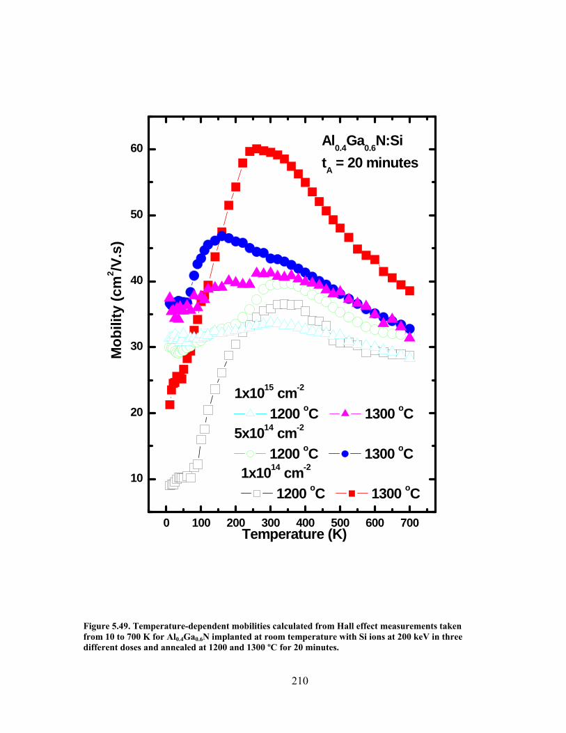
0 100 200 300 400 500 600 700
10
20
30
40
50
60
M
obili
ty (c
m2 /V
.s)
Temperature (K)
1x1015 cm-2
1200 oC 1300 oC5x1014 cm-2
1200 oC 1300 oC1x1014 cm-2
1200 oC 1300 oC
Al0.4Ga0.6N:SitA = 20 minutes
Figure 5.49. Temperature-dependent mobilities calculated from Hall effect measurements taken from 10 to 700 K for Al0.4Ga0.6N implanted at room temperature with Si ions at 200 keV in three different doses and annealed at 1200 and 1300 ºC for 20 minutes.
210

211
at 1300 ºC occur at lower sample temperatures than the mobilities for the samples
annealed at 1200 ºC. As the implanted silicon dose is increased, the mobility curves
become more temperature-independent. The sample implanted with 1x1014 cm-2 silicon
ions and annealed at 1300 ºC has the highest mobility of 60 cm2/V·s at 260 K. The peak
mobilities for the samples implanted with 5x1014 cm-2 are 40 and 57 cm2/V·s which are
slightly lower than those of the samples implanted with the highest dose, 42 and 34
cm2/V·s, for anneal temperatures or 1200 and 1300 ºC, respectively. The degeneracy of
the Si-implanted Al0.4Ga0.6N can be noticed by the relatively high mobilities at 10 K
where the mobility of a non-degenerate sample would approach zero. The mobility at
10K for the samples implanted with silicon doses of 1x10¹⁴, 5x10¹⁴, and 1x1015 cm-2 and
annealed at 1200 ºC are 9, 30, and 31 cm2/V·s. The mobilities for the samples annealed
at 1300 ºC are all higher than those of the samples annealed at 1200 ºC. The mobilities
for the samples annealed at 1300 ºC are 21, 37, and 37 cm2/V·s for the three implanted
silicon doses, respectively. The degenerate impurity band causes the low temperature
mobility to be temperature-independent and is seen here to increase with doping level and
also anneal temperature.
The temperature-dependent mobility curve for the samples implanted with 1x10¹⁴
cm-2 silicon ions most resembles that which is predicted for a non-degenerate sample,
more so for the Al0.4Ga0.6N than for the AlxGa1-xN with Al mole fractions of 10 to 30%.
The Al0.1Ga0.9N and Al0.2Ga0.8N had mobility curves that were more flat and temperature-
independent for the samples implanted with 5x10¹⁴ and 1x1015 cm-2 silicon ions than they
are for the Al0.4Ga0.6N. Also, the lower Al mole fraction material had mobilities that
clearly increased with decreasing implanted silicon dose, which is not the case here. The
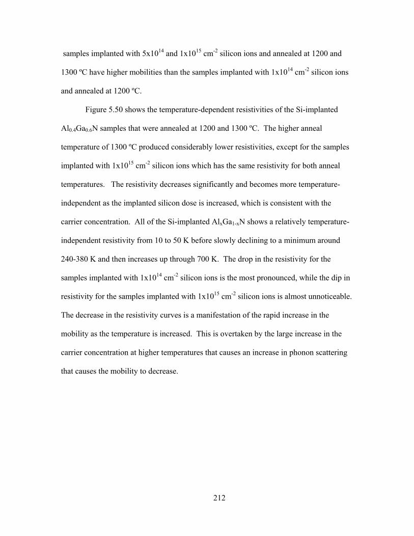
212
samples implanted with 5x10¹⁴ and 1x1015 cm-2 silicon ions and annealed at 1200 and
1300 ºC have higher mobilities than the samples implanted with 1x1014 cm-2 silicon ions
and annealed at 1200 ºC.
Figure 5.50 shows the temperature-dependent resistivities of the Si-implanted
Al0.4Ga0.6N samples that were annealed at 1200 and 1300 ºC. The higher anneal
temperature of 1300 ºC produced considerably lower resistivities, except for the samples
implanted with 1x1015 cm-2 silicon ions which has the same resistivity for both anneal
temperatures. The resistivity decreases significantly and becomes more temperature-
independent as the implanted silicon dose is increased, which is consistent with the
carrier concentration. All of the Si-implanted AlxGa1-xN shows a relatively temperature-
independent resistivity from 10 to 50 K before slowly declining to a minimum around
240-380 K and then increases up through 700 K. The drop in the resistivity for the
samples implanted with 1x1014 cm-2 silicon ions is the most pronounced, while the dip in
resistivity for the samples implanted with 1x1015 cm-2 silicon ions is almost unnoticeable.
The decrease in the resistivity curves is a manifestation of the rapid increase in the
mobility as the temperature is increased. This is overtaken by the large increase in the
carrier concentration at higher temperatures that causes an increase in phonon scattering
that causes the mobility to decrease.

0 20 40 60 80 1000
100
200
300
400
500
2500
5000
7500
10000
12500
15000
17500
Temperature (K)
Al0.4Ga0.6N:SitA = 20 minutes
1x1015 cm-2
1200 oC 1300 oC
5x1014 cm-2
1200 oC 1300 oC
1x1014 cm-2
1200 oC 1300 oC
Shee
t Res
istiv
ity (Ω
/sq.
)
1000/T (K-1)
700 100 50 25 20 15 10
Figure 5.50. Temperature-dependent resistivity calculated from Hall effect measurements taken from 10 to 700 K for Al0.4Ga0.6N that had been implanted at room temperature with silicon ions at 200 keV with doses of 1x10¹⁴, 5x10¹⁴, and 1x1015 cm-2 and annealed at 1200 and 1300ºC for 20 minutes in flowing nitrogen.
213

214
Low Temperature Cathodoluminescence Measurements
Cathodoluminescence measurements were taken at an electron energy of 10 keV
with 50 µA of source current, the temperature in the chamber was 7.4 K, and the slits on
the spectrometer were 400 µm both at the entrance and the exit. The range scanned was
1800 to 7000 Å at a step size of 2 Å with an integration time of 0.1 second.
The spectrum of the unimplanted samples shown as a function of anneal
temperature are shown in Figure 5.51. To gauge the effects of annealing on the
implanted samples the behavior of the unimplanted samples must first be observed. The
CL spectrum for the as-grown sample has a strong neutral donor bound exciton peak at
4.41 eV. The spectra of the as-grown sample exhibits two phonon coupled replicas
separated by 80 meV on the low energy side of the (Do,X) peak at 4.33 and 4.25 eV (49).
Annealing the as-grown material changes the luminescence properties immensely. The
spectrum of the sample annealed at 1200 ºC has been reduced by a factor of 3. This
spectrum has a very intense broad peak centered at 3.78 eV and also shows the
development of some peaks on the low energy side of the peak at 3.78 eV. Increasing the
temperature to 1250 ºC causes the 3.78 eV peak to decrease in intensity and the lower
energy peaks that began to emerge in the spectra for the sample annealed at 1200 ºC are
considerably enhanced. The energies of these peaks are 3.75, 3.64, 3.53, 3.41, 3.29, 3.17,
3.05, 2.92, 2.78, and 2.64 eV. The spacing in between the peaks increases slightly from
110 to 140 meV as the energy of the peaks decreases. The CL spectra for the samples
annealed at 1300 ºC show no evidence of this broad luminescence instead it had an
excellent (Do,X) peak centered at 4.41 eV with two phonon replicas at 4.33 and 4.25 eV,
as seen in the spectrum of the as-grown sample. The spectrum for the sample annealed at
1300 ºC was more intense than the as-grown sample and the spectrum had to be reduced

2 3 4 5 6
Wavelength (nm)
4.25 eV
4.33 eV
Unimplanted Al0.4Ga0.6NT=7.4 K
x1/3
1350 oC
3.78 eV
C
L In
tens
ity (a
rb. u
nits
)
Energy (eV)
4.41 eV
As-grown
1300 oC
1250 oC
1200 oC
x1/25
700 500 400 300 200
Figure 5.51. CL spectra taken at 7.4 K for unimplanted Al0.4Ga0.6N that have been anneal at 1200, 1250, 1300, and 1350 ºC for 20 minutes in flowing nitrogen.
215

216
by a factor 25. Further increasing the anneal temperature to 1350 ºC produces a CL
spectrum that resembles that of the samples annealed at 1250 ºC in that there was no
evidence of the (Do,X) peak only a broad luminescence that consisted of 10 individual
peaks. Similar oscillations were seen by Lee et al. for Mg-doped AlxGa1-xN with Al mole
fractions from less than 0.1. They observed the same oscillations and attributed the peak
at 3.3 eV to be a free electron transitioning to a Mg acceptor and the other peaks to be
interference patterns (76). They also observed that the peak position of the free electron
to Mg acceptor transition blueshifts from 3.30 to 3.35 as the Al mole fraction of the
material was increased from 0.05 to 0.09. This luminescence is obviously not due to Mg
acceptors, but it could be related to reduction of the crystalline quality with increasing Al
content which can increase the number of Al vacancies that act as deep acceptors in
AlxGa1-xN (44). The spectra for the samples annealed at all of the temperatures except
1300 ºC exhibit this lower energy luminescence.
The low temperature CL spectra for the Si-implanted Al0.4Ga0.6N annealed for 20
minutes at 1300 ºC are shown in Figure 5.52. All of the spectra show a (Do,X) peak at
4.41 eV and two phonon coupled replicas separated by 80 meV on the low energy side of
the (Do,X) peak at 4.33 and 4.25 eV (49). The intensities of the (Do,X) peak for the
unimplanted sample and the sample implanted with 1x1014 cm-2 silicon ions are much
stronger than those of the other implanted samples and their spectrums have been
decreased by a factor of 5. The sample implanted with a dose of 1x1014 cm-2 silicon ions
has a (Do,X) peak with higher intensity than the unimplanted sample, indicating excellent
recovery of the lattice damage and incorporation of the implanted silicon ions. The
samples implanted with a dose of 5x1014 cm-2 silicon ions have a CL spectrum that has
broadened due to band tailing effects from the increased carrier concentration. The

2 3 4 5 6
4.25 eV
4.33 eV
Wavelength (nm)
2.8 eV
x1/5
x1/5
C
L In
tens
ity (a
rb. u
nits
)
Energy (eV)
Si-implanted Al0.4Ga0.6N
Anneal: 1300oC/ 20 min.T=7.4 K
4.41 eV
1x1014 cm-2
1x1015 cm-2
5x1014 cm-2
Unimplanted
700 500 400 300 200
Figure 5.52. CL spectra taken at 7.4 K for Al0.4Ga0.6N that have been anneal at 1300 ºC for 20 minutes in flowing nitrogen.
217

218
spectrum for this sample also shows a broad band of luminescence centered around 2.8
eV that could be similar to the luminescence observed for the unimplanted samples. The
sample implanted with 1x1015 cm-2 silicon ions has a also has a broadened (Do,X) peak
with evidence of the two phonon replicas, but does not exhibit the broad band
luminescence centered around 2.8 eV. Like the AlxGa1-xN with lower Al mole fractions
the intensity of the (Do,X) peak decreased as the implanted dose was increased.
However, the sample implanted with 5x1014 cm-2 silicon ions have the most degraded
optical properties.
The low temperature CL spectra for the Al0.4Ga0.6N implanted with 1x1014 cm-2
silicon ions and annealed for 20 minutes at various temperatures are shown in Figure
5.53. All of the anneal temperatures produced a good (Do,X) peak centered at 4.41 eV
and evidence of two phonon coupled replicas separated by 80 meV on the low energy
side of the (Do,X) peak at 4.33 and 4.25 eV (49) in their CL spectra.
The spectra for the samples annealed at 1200 and 1250 ºC are very similar, only
the sample annealed at 1250 ºC has a more intense (Do,X) peak. The phonon peaks for
the samples implanted with this dose and annealed at 1200 and 1250 ºC are clearly
identifiable. However, as the anneal temperature is increased the carrier concentration
increases, thus increasing the effects of band tailing causing the peaks to broaden and
merge together, as seen in the spectra for the samples annealed at higher temperatures.
The intensity of the (Do,X) peak increases as the anneal temperature is increased, except
for the sample annealed at 1300 ºC which shows diminished intensity for unknown
reasons. However, as seen in the previous figure, the spectra for the samples annealed at
1300 ºC shows a sharp (Do,X) peak that has similar intensity as the as-grown sample.
None of the samples implanted with 1x1014 cm-2 silicon ions exhibit any broad
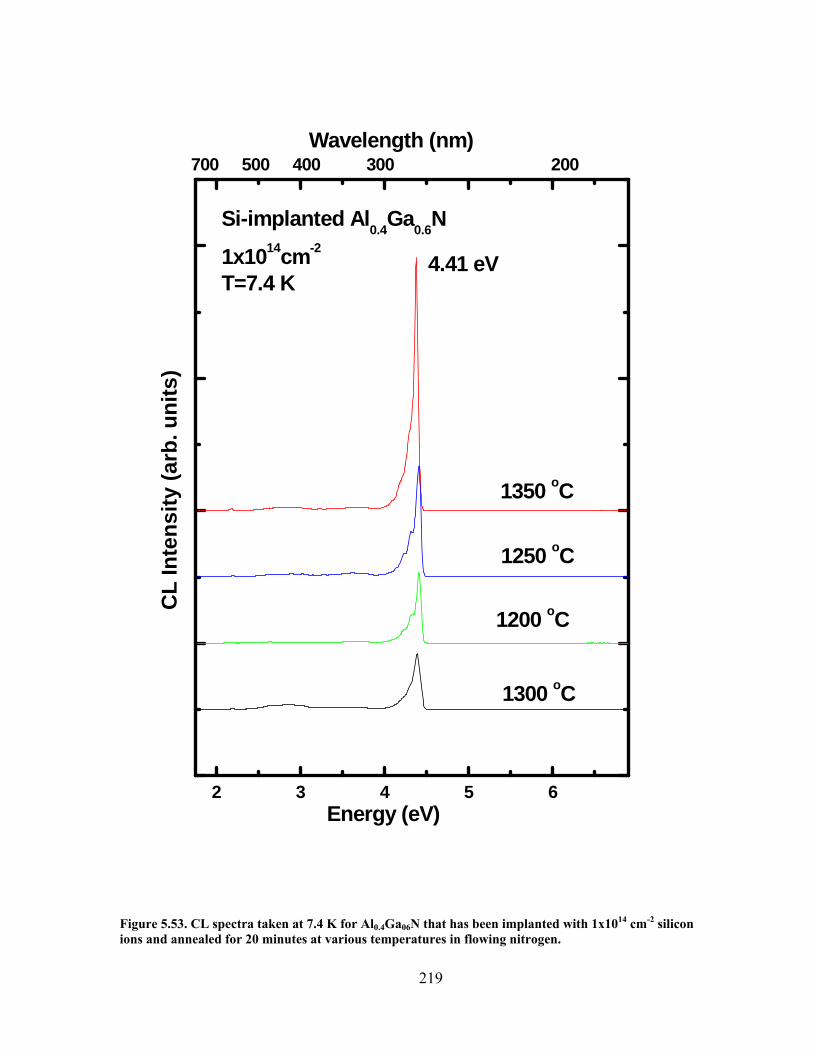
2 3 4 5 6
Wavelength (nm)
4.41 eV
C
L In
tens
ity (a
rb. u
nits
)
Energy (eV)
Si-implanted Al0.4Ga0.6N
1x1014cm-2
T=7.4 K
1350 oC
1300 oC
1250 oC
1200 oC
700 500 400 300 200
Figure 5.53. CL spectra taken at 7.4 K for Al0.4Ga06N that has been implanted with 1x1014 cm-2 silicon ions and annealed for 20 minutes at various temperatures in flowing nitrogen.
219

220
luminescence at lower energies, as was seen for the Al0.1Ga0.9N. The intensity of the
(Do,X) peak increases as the anneal temperature is increased from 1200 to 1350 ºC,
signifying successive improvement in the crystal lattice with each increase in the anneal
temperature. The increase in intensity of the (Do,X) peaks observed for the samples
annealed at temperatures of 1200, 1250, and 1350 ºC indicate that more of the implanted
silicon ions have become electrically active as the anneal temperature was increased.
These CL spectra agree very well with the electrical activation results obtained
from Hall effect measurements for the samples implanted with this silicon dose. The
strong intensity of the (Do,X) peak and the band tailing effects seen in the spectra of the
sample annealed at 1350 ºC anneal correlate well with the high activation obtained for
this sample. The (Do,X) peak and the high mobilities observed on the samples implanted
with the lowest silicon dose indicate excellent recovery of the radiation damage caused
during the ion implantation after annealing at 1350 ºC for 20 minutes in flowing
nitrogen.
The CL spectra of the samples implanted with a silicon dose of 5x1014 cm-2 and
annealed for 20 minutes at various temperatures are shown in Figure 5.54. Not all of the
spectrum have the (Do,X) peak at 4.41 eV and the phonon related peaks. The sample
annealed at 1200 ºC exhibit a strong (Do,X) peak along with some weak luminescence
centered around 2.8 eV that could be similar to the broad emission in the spectra for the
unimplanted samples. Increasing the anneal temperature to 1250 ºC causes the peak
position to shift to 4.37 eV however there is still evidence of the phonon replicas. This
spectrum has an increased broad luminescence centered at 2.8 eV. Nam et al. attribute
the origin of this luminescence to the be the same as that of the yellow luminescence
found in GaN at 2.15 eV, which is still under debate, however it is generally accepted to

2 3 4 5 6
Wavelength (nm)
3.80 eV
4.37 eV
4.41 eV
C
L In
tens
ity (a
rb. u
nits
)
Energy (eV)
1250 oC
Si-implanted Al0.4Ga0.6N
5x1014cm-2
T=7.4 K
1350 oC
1300 oC
1200 oC2.8 eV
700 500 400 300 200
Figure 5.54. CL spectra taken at 7.4 K for Al0.4Ga0.6N that was implanted with 5x1014 cm-2 silicon ions and annealed at various temperatures for 20 minutes in flowing nitrogen.
221

222
be related to a donor acceptor pair transition with a shallow donor and deep acceptor that
could be an aluminum vacancy or vacancy complex (44). The (Do,X) peak in the spectra
for the samples annealed at 1300 ºC is similar in intensity and shape to the sample
annealed at 1200 ºC. However, the intensity of the broad luminescence centered at 2.8
eV is more enhanced for the sample annealed at 1300 ºC. The sample annealed at 1350
ºC has a unique spectrum with a broad peak centered at 3.8 eV that has a shoulder that
extends out to 3.3 eV. This is similar to a peak reported by McFall et al, who observed a
donor bound acceptor pair (DAP) peak at 3.82 eV in Si-doped Al0.5Ga0.5N and a phonon
replica at 3.72 eV (49).
The CL spectra indicate that for the samples implanted with this silicon dose were
generally recovered from the ion implantation induced damage. The silicon electrical
activation for these samples gradually increased as the anneal temperature was increased
to 1350 ºC. However, there is only a 1% difference in the activation between the samples
annealed at 1300 and 1350 ºC. Electrical efficiencies for the samples implanted with
5x1014 cm-2 silicon ions increases dramatically as the anneal temperature is raised from
1200 to 1300 ºC.
The CL spectra of the samples implanted with the a silicon dose of 1x1015 cm-2
and annealed for 20 minutes at various temperatures are shown in Figure 5.55. The
samples annealed from 1200 to 1300 ºC all have a (Do,X) peak centered at 4.41 eV,
whose intensity increases as the anneal temperature is increased. The spectrum for the
sample annealed at 1350 ºC does not have any features in common with the spectra of the
other samples. The samples annealed at 1200 ºC show a weak peak that has red shifted to
4.33 eV and the broad luminescence at 2.8 eV, which is similar to the spectrum of the
Al0.4Ga0.6N sample implanted with 5x1014 cm-2 silicon ions and annealed at 1250 ºC. The

2 3 4 5 6
Wavelength (nm)
3.43 eV
4.41 eV
4.33 eV
C
L In
tens
ity (a
rb. u
nits
)
Energy (eV)
Si-implanted Al0.4Ga0.6N
1x1015cm-2
T=7.4 K
1250 oC
1300 oC
1200 oC
1350 oC
700 500 400 300 200
Figure 5.55. CL spectra taken at 7.4 K for Al0.4Ga0.6N that was implanted with 1x1015 cm-2 silicon ions and annealed at various temperatures for 20 minutes in flowing nitrogen.
223

224
sample annealed at 1250 ºC shows recovery of the (Do,X) peak at 4.41 eV and the has a
broad shoulder for the lower energy phonon replicas. The peak has broadened
considerably towards the lower energy due to band tailing effects, and the two low
energy peaks are seen as shoulder peaks. The spectra for the sample annealed at 1300 ºC
has the strongest (Do,X) peak with the two low energy peaks seen as shoulders. The
spectra for the sample annealed at 1350 ºC shows a broad band luminescence that is
centered at 3.43 eV. This sample has a spectrum similar to that of the Al0.4Ga0.6N sample
implanted with 5x1014 cm-2 silicon ions and annealed at 1350 ºC, only what was seen as a
broad, wide shoulder has now developed into an etalon effect of the donor acceptor pair
peak identified by Mcfall et al. at 3.82 eV (49). This type of luminescence was also seen
in the spectra for the unimplanted samples that were annealed at this temperature
suggesting that is could be caused from anneal related damage.
Silicon Implanted Al0.5Ga0.5N
In the last few years the emerging importance of high mole fraction AlxGa1-xN for
device applications has become prevalent sparking an increase in research regarding
silicon doping of AlxGa1-xN with Al concentrations 50% or above. Yoshitaka et al.
investigated the effects of Si-doping on AlxGa1-xN and AlN alloys. AlxGa1-xN with Al
concentrations above 50% were found to exhibit a sharp decrease in the electron
concentration and a spike in resistivity by 5 orders of magnitude (53). Silicon was found
to act as a donor over the entire range of Al content however; there is an upper Si-doping
limit at which n-type conduction is obtained that decreases with increasing Al content.
Additional silicon ions form an acceptor state that compensates the silicon donors
producing a highly resistive material (53). They reported that the ionization energy of

225
AlxGa1-xN with Al concentration less than 0.49 slowly increases from 8.1 to 12 meV as
the Al concentration was increased. When the Al content is greater than 0.49, the
ionization energy increases at a greater rate going from 12 meV for Al0.49Ga0.51N to 86
meV for AlN.
There are no reported ionization energies for Si-implanted Al0.5Ga0.5N. The
ionization energy can be extracted from Hwang et al. who determined that the donor
ionization energy of AlxGa1-xN increases with increasing Al mole fraction from 34 meV
for GaN to 90 meV for AlN, by using hydrogen atom model (51). Assuming the
ionization energy increases linearly the ionization energy for Si in Al0.5Ga0.5N would then
be on the order of 61 meV for a non-degenerate sample. The implanted silicon doses of
1x10¹⁴, 5x10¹⁴, and 1x1015 cm-2 correspond to peak volume carrier concentrations of
5.78x10¹⁸, 2.89x10¹⁹ and 5.78x1019 cm-3, which all exceed the Mott concentration of
4.16x1018 cm-3 for Al0.5Ga0.5N. The Si-implanted Al0.5Ga0.5N samples will be degenerate
and therefore will underestimate the actual ionization energies.
Room Temperature Hall Effect Measurements
The MEMOCVD grown Al0.5Ga0.5N was capped with 500Å of AlN and
implanted at room temperature with silicon ions at 200 keV in three different doses. The
silicon doses were 1x10¹⁴, 5x10¹⁴, and 1x1015 cm-2 and the effective doses are 9.93x10¹³,
4.96x10¹⁴, and 9.93x1014 cm-2, respectively after taking into account the 500Å AlN cap.
The samples were annealed from 1200 to 1350 ºC for 20 minutes in a nitrogen
environment. All the samples had excellent surface morphology following the anneal at
1350 ºC. Room temperature Hall effect measurements were conducted to determine
sheet carrier concentrations for the samples and are shown in Figure 5.56. The
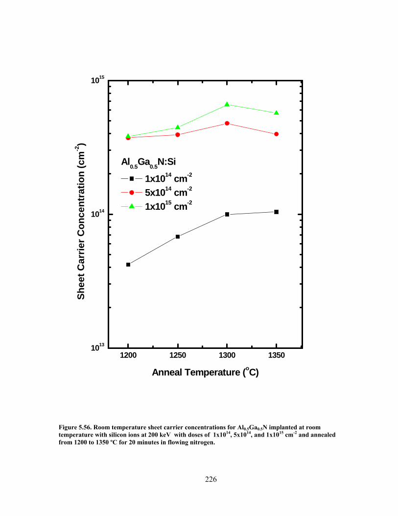
1200 1250 1300 13501013
1014
1015
Shee
t Car
rier C
once
ntra
tion
(cm
-2)
Anneal Temperature (oC)
Al0.5Ga0.5N:Si
1x1014 cm-2
5x1014 cm-2
1x1015 cm-2
Figure 5.56. Room temperature sheet carrier concentrations for Al0.5Ga0.5N implanted at room temperature with silicon ions at 200 keV with doses of 1x10¹⁴, 5x10¹⁴, and 1x1015 cm-2 and annealed from 1200 to 1350 ºC for 20 minutes in flowing nitrogen.
226

227
unimplanted samples, both as-grown and annealed, were highly resistive making it
impossible to collect any meaningful data. Thus, the silicon electrical activation was
calculated using the measured room temperature carrier concentration with no correction
for the background carriers.
The room temperature sheet carrier concentrations for the samples implanted with
1x1014 cm-2 silicon ions behave differently from the samples implanted with the other
silicon doses. The carrier concentration for the Al0.5Ga0.5N implanted with a dose of
1x1014 cm-2 silicon ions increases linearly as the anneal temperature is raised from 1200
to 1300 ºC. The carrier concentration begins to saturate for the samples annealed at
1350 ºC. Like the AlxGa1-xN with the lower Al mole fractions, these samples also show
the most dramatic change in carrier concentration as the anneal temperature is increased.
The carrier concentrations for the Al0.5Ga0.5N implanted with 1x1014 cm-2 silicon ions
increases from 4.2x10¹³ to 1.04x1014 cm-2 as the anneal temperature is raised from 1200
to 1350 ºC, respectively. The carrier concentrations for the Al0.5Ga0.5N implanted with
5x10¹⁴ and 1x1015 cm-2 silicon ions have a similar dependence on the anneal temperature.
The carrier concentration for these samples increases slightly as the anneal temperature is
raised from 1200 to 1250 ºC. The increase in carrier concentration is more significant
when the anneal temperature is raised to 1300 ºC for these samples. The samples
implanted with both silicon doses exhibit their peak carrier concentrations after being
annealed at 1300 ºC for 20 minutes in a nitrogen environment. The carrier concentration
decreases for the samples implanted with 5x10¹⁴ and 1x1015 cm-2 silicon ions after being
annealed at 1350 ºC. The carrier concentration for the Al0.5Ga0.5N implanted with a dose
of 5x1014 cm-2 silicon ions reaches a maximum carrier concentration of 4.8x1014 cm-2
while the sample implanted with 1x1015 cm-2 reaches a maximum carrier concentration of

228
6.6x1014 cm-2. The carrier concentrations for the Al0.5Ga0.5N implanted with a dose
1x1015 cm-2 silicon ions are considerably lower than those of achieved for the AlxGa1-xN
with the lower Al mole fractions. However, the carrier concentrations for the Al0.1Ga0.9N
and Al0.4Ga0.6N samples implanted with this silicon dose also declined as the anneal
temperatures reached their upper range.
The silicon electrical activation is closely related to the carrier concentration and
has the same trends with the anneal temperature as mentioned above. The electrical
activations for the Al0.5Ga0.5N were calculated using the effective doses and room
temperature sheet carrier concentrations and the results are shown in Figure 5.57. Unlike
the AlxGa1-xN with lower Al mole fractions, the Al0.5Ga0.5N exhibit excellent activation
for the samples implanted with 1x1014 cm-2 silicon ions. The samples implanted with this
dose experience higher silicon activation as the anneal temperatures are increased from
1200 to 1350 ºC. The samples implanted with 1x1014 cm-2 silicon ions reach 100%
activation after being annealed for 20 minutes at 1300 ºC and 104% following the 1350
ºC anneal. Activation efficiency greater than 100% is unrealistic and could be due to an
underestimate of the effective dose. This is the best activation for samples implanted
with this dose for all the Al concentrations of AlxGa1-xN investigated. The activation
efficiency for the samples implanted with 5x10¹⁴ and 1x1015 cm-2 silicon ions peak after
being annealed at 1300 ºC. The activation efficiency for these samples declines as the
anneal temperature is raised to 1350 ºC. The samples implanted with 5x1014 cm-2 silicon
ions experience a peak activation of 96% following the anneal at 1300 ºC for 20 minutes.
The activation of the samples implanted with this dose and annealed at 1350 ºC drops to
80%, which is the same as the activation achieved for the samples annealed at 1250 ºC.
The activation efficiencies of the samples implanted with the highest silicon dose of
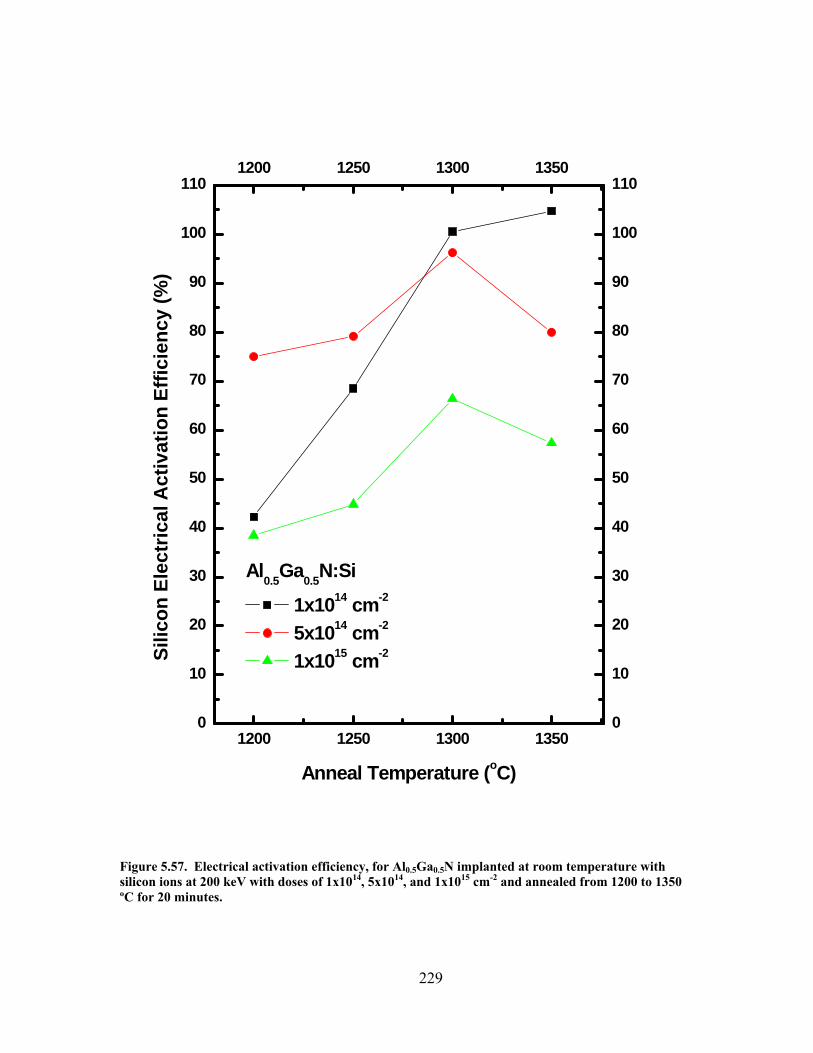
1200 1250 1300 1350
1200 1250 1300 1350
0
10
20
30
40
50
60
70
80
90
100
110
0
10
20
30
40
50
60
70
80
90
100
110
Silic
on E
lect
rical
Act
ivat
ion
Effic
ienc
y (%
)
Anneal Temperature (oC)
Al0.5Ga0.5N:Si
1x1014 cm-2
5x1014 cm-2
1x1015 cm-2
Figure 5.57. Electrical activation efficiency, for Al0.5Ga0.5N implanted at room temperature with silicon ions at 200 keV with doses of 1x10¹⁴, 5x10¹⁴, and 1x1015 cm-2 and annealed from 1200 to 1350 ºC for 20 minutes.
229

230
1x1015 cm-2 reaches 66% after being annealed at 1300 ºC for 20 minutes in a nitrogen
ambient. The samples implanted with the highest silicon dose had the lowest activation
efficiencies and increasing the anneal temperature to 1350 ºC caused the activation for
these samples to decline. Thus, the optimal anneal temperature for the Al0.5Ga0.5N
implanted with a dose of 1x1015 cm-2 silicon ions is less then 1350 ºC and an anneal time
of 20 minutes is insufficient.
This behavior is inconsistent with the AlxGa1-xN samples with lower Al mole
fractions implanted with 1x1015 cm-2 silicon ions, which all had activation efficiencies
higher than 96% under various annealing conditions. This decline in activation could be
related to the upper silicon doping limit referred to by Yoshitaka et al. at which point the
silicon ions begin to act as acceptors (53). All of the implanted samples show
considerable activation efficiencies in Al0.5Ga0.5N however, the activation increases as
the implantation dose is decreased as is illustrated in Figure 5.58, which is a shift in
behavior from the AlxGa1-xN with lower Al concentrations.
Based on the electrical activation efficiencies of the implanted silicon the optimal
anneal temperature for the Si-implanted Al0.5Ga0.5N is 1300 ºC. The samples implanted
with 1x10¹⁴ and 5x1014 cm-2 silicon ions reach activations of 100% and 96% after being
annealed at this temperature for 20 minutes. The Al0.5Ga0.5N implanted with a dose of
1x1015 cm-2 silicon ions has a lower activation of 66% at this temperature however,
further increasing the anneal temperature to 1350 ºC has negative effects on the
activation, indicating that extending the anneal time at 1300 ºC could improve the
activation. The optimal anneal temperature for the Si-implanted Al0.5Ga0.5N was not as
dependent on the implanted as it was for the AlxGa1-xN with lower Al concentrations.
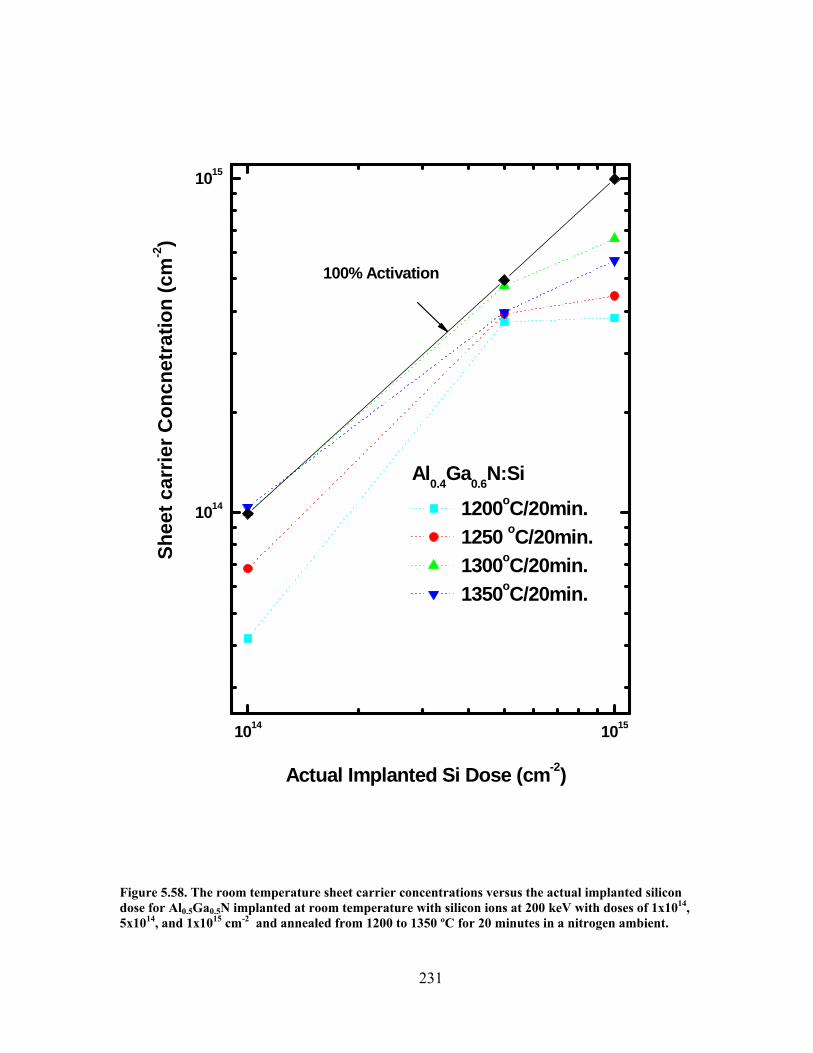
1014 1015
1014
1015
Al0.4Ga0.6N:Si
1200oC/20min. 1250 oC/20min. 1300oC/20min. 1350oC/20min.
Actual Implanted Si Dose (cm-2)
Shee
t car
rier C
oncn
etra
tion
(cm
-2)
100% Activation
Figure 5.58. The room temperature sheet carrier concentrations versus the actual implanted silicon dose for Al0.5Ga0.5N implanted at room temperature with silicon ions at 200 keV with doses of 1x10¹⁴, 5x10¹⁴, and 1x1015 cm-2 and annealed from 1200 to 1350 ºC for 20 minutes in a nitrogen ambient.
231

232
The resistivities for the Si-implanted Al0.5Ga0.5N that have been annealed for 20
minutes at various temperatures are shown in Figure 5.59. The sample implanted with
1x1014 cm-2 silicon ions has a resistivity of 6.6 kΩ/ which is 10 times higher than the
resistivity of the samples implanted with 5x10¹⁴ and 1x1015 cm-2 silicon ions when
annealed at 1200 ºC for 20 minutes. The resistivity for the samples implanted with the
lowest silicon dose falls about 5.5 kΩ/ as the anneal temperature is increased to
1350 ºC. Unlike the AlxGa1-xN with lower Al mole fractions, only the resistivity of the
samples implanted with 1x1014 cm-2 silicon ions decrease as the anneal temperature is
increased, due to the increase in the carrier concentration. The resistivity for the samples
implanted with 5x10¹⁴ and 1x1015 cm-2 silicon ions decreases as the anneal temperature is
increased from 1200 to 1300 ºC, but then the resistivity increases for the samples
annealed at 1350 ºC due to a decrease in the carrier concentration. The resistivity for
Al0.5Ga0.5N implanted with 1x1014 cm-2 silicon ions decreases from 6.6 kΩ/ to 1.1 kΩ/
as the anneal temperature is raised from 1200 to 1350 ºC, respectively. The lowest
resistivity for the Al0.5Ga0.5N implanted with 5x1014 cm-2 silicon ions is of 362 Ω/ and
occurred for the samples annealed at 1300 ºC. The samples implanted with 1x1015 cm-2
silicon ions showed a slightly linear decrease in resistivity as the anneal temperature is
increased from 1250 to 1300 ºC dropping from 674 Ω/ to 270 Ω/, respectively.
However the resistivity for the samples implanted with this dose and annealed at 1350 ºC
increases to 352 Ω/.
The anneal temperature that produces the lowest resistivity corresponds to the
temperature at which the samples have a maximum in carrier concentration, and thus
activation for all of the implanted silicon doses, as expected. The dependence of the
resistivity on the anneal temperature of the Si-implanted Al0.5Ga0.5N are similar to the

1200 1250 1300 1350 14000
100
200
300
400
500
600
700
800
900
1000
1100
1200
1300
1400
2500
5000
Res
istiv
ity (Ω
/[ ])
Anneal Temperature (oC)
Al0.5Ga0.5N:Si
1x1014 cm-2
5x1014 cm-2
1x1015 cm-2
Figure 5.59. Room temperature resistivity measurements taken under zero magnetic field for Al0.5Ga0.5N implanted at room temperature with silicon ions at 200 keV with doses of 1x10¹⁴, 5x10¹⁴, and 1x1015 cm-2 and annealed from 1200 to 1350 ºC for 20 minutes in a nitrogen ambient.
233

234
dependence observed in AlxGa1-xN with lower Al concentrations. However, the
magnitude of the resistivity is higher, for samples implanted with each silicon dose, in
Al0.5Ga0.5N than for the AlxGa1-xN with lower Al concentrations.
The room temperature mobilities for all the Si-implanted Al0.5Ga0.5N annealed for
20 minutes at various temperatures are shown in Figure 5.60. The mobility increases as
the anneal temperature is increased from 1200 to 1350 ºC for the samples implanted with
doses of 1x10¹⁴ silicon ions, despite an increase in ionized impurity scattering. The
mobility for the samples implanted with and 1x1015 cm-2 silicon ions also increases as the
anneal temperature is increased. The carrier concentration for the sample implanted with
the highest silicon dose decreases after being annealed at 1350 ºC, thus decreasing the
effects of ionized impurity scattering causing the mobility to increase. The mobility of
the Al0.5Ga0.5N implanted with 5x1014 cm-2 silicon ions increases as the anneal
temperature is raised from 1200 to 1250 ºC, where is reaches a peak of 43 cm2/V·s.
Further increasing the anneal temperature to 1300 ºC causes the mobility to decrease to
36 cm2/V·s which could be caused by an increase in ionized impurity scattering. The
samples implanted with this dose and annealed at 1350 ºC show a slight increase in the
mobility to 38 cm2/V·s due to the decreased effects of ionized impurity scattering,
however this mobility is not as high as it was for the samples annealed at 1250 ºC. The
Al0.5Ga0.5N implanted with a dose of 1x1015 cm-2 silicon ions exhibit a large increase in
mobility as the anneal temperature is raised from 1200 to 1250 ºC. The mobility for these
samples levels off as the anneal temperature is increased further to 1350 ºC. The peak
mobility for the samples implanted with the highest silicon dose was of 35 cm2/V·s which
occurred for the sample annealed at 1350 ºC for 20 minutes. The sample implanted with

1200 1250 1300 1350
20
30
40
50
60
Hal
l Mob
ility
(cm
2 /V.s
)
Anneal Temperature (oC)
Al0.5Ga0.5N:Si
1x1014 cm-2
5x1014 cm-2
1x1015 cm-2
Figure 5.60. The room temperature mobilities calculated from Hall effect measurements on Al0.5Ga0.5N implanted at room temperature with silicon ions with doses of 1x10¹⁴, 5x10¹⁴, and 1x1015 cm-2 and annealed from 1200 ºC to 1350 ºC for 20 minutes in a nitrogen ambient.
235

236
1x1014 cm-2 silicon ions shows a dramatic rise in mobility from 23 cm2/V·s to 55 cm2/V·s
as the temperature is increased from 1200 to 1350 ºC.
The mobility for the Al0.5Ga0.5N is dose dependent, as it has been for all of the
AlxGa1-xN investigated, with the lower doses having higher mobilities. The samples
implanted with a dose of 1x1014 cm-2 silicon ions achieved their peak activation after
annealing at 1350 ºC, which corresponds to the anneal temperature for the peak mobility.
Indicating that with each successive increase in the anneal temperature more lattice
damage is recovered and more of the implanted silicon ions are activated. The samples
implanted with silicon doses of 5x10¹⁴ and 1x1015 cm-2 experience their peak activation at
different anneal temperatures than their peak mobilities, suggesting that most of the
implantation induced damage had been repaired since the effects of ionized impurity
scattering are dominant over those of defect scattering. The samples implanted with the
lowest silicon dose exhibit the largest mobility, as they have for all the AlxGa1-xN
samples with lower Al mole fractions, except for the Al0.4Ga0.6N samples. The peak
mobilities for the Si-implanted Al0.5Ga0.5N are lower than those of the lower Al mole
fraction samples which is lost likely related to the increased effective mass as the Al mole
fraction is increased (33).
To improve the electrical activation efficiency of the Si-implanted Al0.5Ga0.5N the
anneal time was extended from 20 to 40 minutes for a set anneal temperature of 1200 ºC.
A comparison of the results obtained for both the 20 and 40 minute anneals at 1200 ºC
are listed in Table 5.4. The Al0.5Ga0.5N implanted with a dose of 1x1014 cm-2 silicon ions
were not included in the study based on the low activation efficiency achieved after
annealing at 1200 ºC and the poor results obtained from the samples implanted with a
silicon dose of 1x1015 cm-2, which also had a low activation after the 20 minute anneal at

237
1200 ºC. Complete activation has been shown to be achievable for the Si-implanted
Al0.5Ga0.5N however, an anneal temperature of 1200 ºC appears to be too low for this to
take place.
Extending the anneal time to 40 minutes had positive affects on all of the physical aspects
determined from the Hall effect measurements. The carrier concentrations, and therefore
activation energies, of the samples implanted with 5x10¹⁴ and 1x1015 cm-2 silicon ions
increased only slightly for the samples annealed for 40 minutes as opposed to those
annealed for 20 minutes. The samples implanted with 5x1014 cm-2 silicon ions exhibit
less than a 5% increase in the electrical activation efficiency going from 75% to 80% for
the 40 minute anneal. The mobility for the samples implanted with this dose increase
significantly from 27.6 to 39.6 cm2/V·s regardless of the increase in ionized impurity
scattering. The resistivity for these samples decreases 30% by extending the anneal time,
as expected. The electrical activation for the samples implanted with 1x1015 cm-2 silicon
ions increases 5% bringing it up to 44% after the 40 minute anneal. The resistivity for
the samples implanted with this silicon dose and annealed for 40 minutes is almost half
that of the samples annealed for 20 minutes. The mobility for the Al0.5Ga0.5N implanted
with 1x1015 cm-2 silicon ions increases from 24.3 to 40.7 cm2/V·s after the extended time
anneal, despite the increase in ionized impurity scattering. This is the highest mobility
obtained for an Al0.5Ga0.5N sample implanted with 1x1015 cm-2 silicon ions.
All the samples showed an increase in activation from extending the anneal time
to 40 minutes; however the improvement was not always significant enough to achieve
an activation better than that achieved at a higher annealing temperature. The samples
implanted with a dose of 5x1014 cm-2 silicon ions, as well as the samples implanted with
1x1015 cm-2 silicon ions, have the same activation for the samples annealed at 1200 ºC

238
Table 5.4. Room temperature Hall effect results for Al0.5Ga0.5N implanted at room temperature with silicon ions at 200 keV in three doses and annealed at 1200 ºC for 20 or 40 minutes nitrogen ambient.
Dose
(cm-2) Time (min.)
Carrier Concentration
(cm-2) Activation (%) Resistivity
(Ω/) Mobility
(cm2/V·s)
5x10¹⁴ 20 3.72x10¹⁴ 74 .98 607.89 27.59
5x10¹⁴ 40 3.96x10¹⁴ 79.76 428.93 39.55
1x10¹⁵ 20 3.82x10¹⁴ 38.47 674 24.26
1x10¹⁵ 40 4.39x10¹⁵ 44.21 349.93 40.66
for 40 minutes and 1250 ºC for 20 minutes. Despite having the same activation the other
physical properties of the Al0.5Ga0.5N, such as resistivity and mobility, do not respond to
the lengthened anneal time the same way. The resistivity of the samples implanted with
5x1014 cm-2 silicon ions and annealed at 1250 ºC have a 58 Ω/ lower resistivity and a
3 cm2/V·s higher mobility than the samples implanted with this dose and annealed at
1200 ºC for 40 minutes. The Al0.5Ga0.5N implanted with 1x1015 cm-2 silicon ions exhibit
the opposite behavior, the samples annealed at 1200 ºC for 40 minutes have a lower
resistivity and a higher mobility than the samples implanted with this dose and annealed
at 1250 ºC for 20 minutes. The resistivity of the samples implanted with this dose and
annealed for 40 minutes is lower by 22 Ω/ and the mobility increases by 7 cm2/V·s over
the samples annealed at 1250 ºC for 20 minutes.
The Al0.5Ga0.5N implanted with a dose of 5x10¹⁴ and 1x1015 cm-2 silicon ions
reach their peak activation efficiencies after being annealed for 20 minutes at 1300 ºC.

239
Their peak activations for the samples annealed at this temperature are 16% and 20%
higher than the activations achieved for the samples annealed at 1200 ºC for 40 minutes.
Annealing the Al0.5Ga0.5N at 1200 ºC for 40 minutes did not significantly increase the
activation efficiency of the implanted samples as it had for the AlxGa1-xN with lower Al
concentrations. An anneal temperature of 1200 ºC does not appear to be high enough for
complete activation of the implanted silicon to occur in Al0.5Ga0.5N.
The Si-implanted Al0.5Ga0.5N implanted with a doses of 1x10¹⁴ and 5x1014 cm-2
achieved high electrical activation efficiency above 95% for the samples annealed at
1300 ºC for 20 minutes. The samples implanted with the lowest silicon dose had the best
activation of 100% and the activation for the samples implanted with 5x1014 cm-2 silicon
ions was only slightly lower at 96%. The samples implanted with the highest silicon dose
of 1x1015 cm-2 had the lowest peak activation efficiency of 66% for the samples annealed
at 1300 ºC for 20 minutes. The Si-implanted Al0.5Ga0.5N samples deviate in behavior
from the AlxGa1-xN material with lower Al mole fractions. The Al0.5Ga0.5N samples are
the only AlxGa1-xN samples to achieve higher activation efficiencies for the samples
implanted the lowest silicon dose than the samples implanted with the highest silicon
dose. The peak activation for the AlxGa1-xN with Al concentrations of 10 to 40%
increases as the implanted silicon dose increases, except for the Al0.4Ga0.6N which had
excellent activation for all three implanted silicon doses. The opposite is true for the
Al0.5Ga0.5N which exhibit a decrease in activation as the implanted silicon dose in
increased.
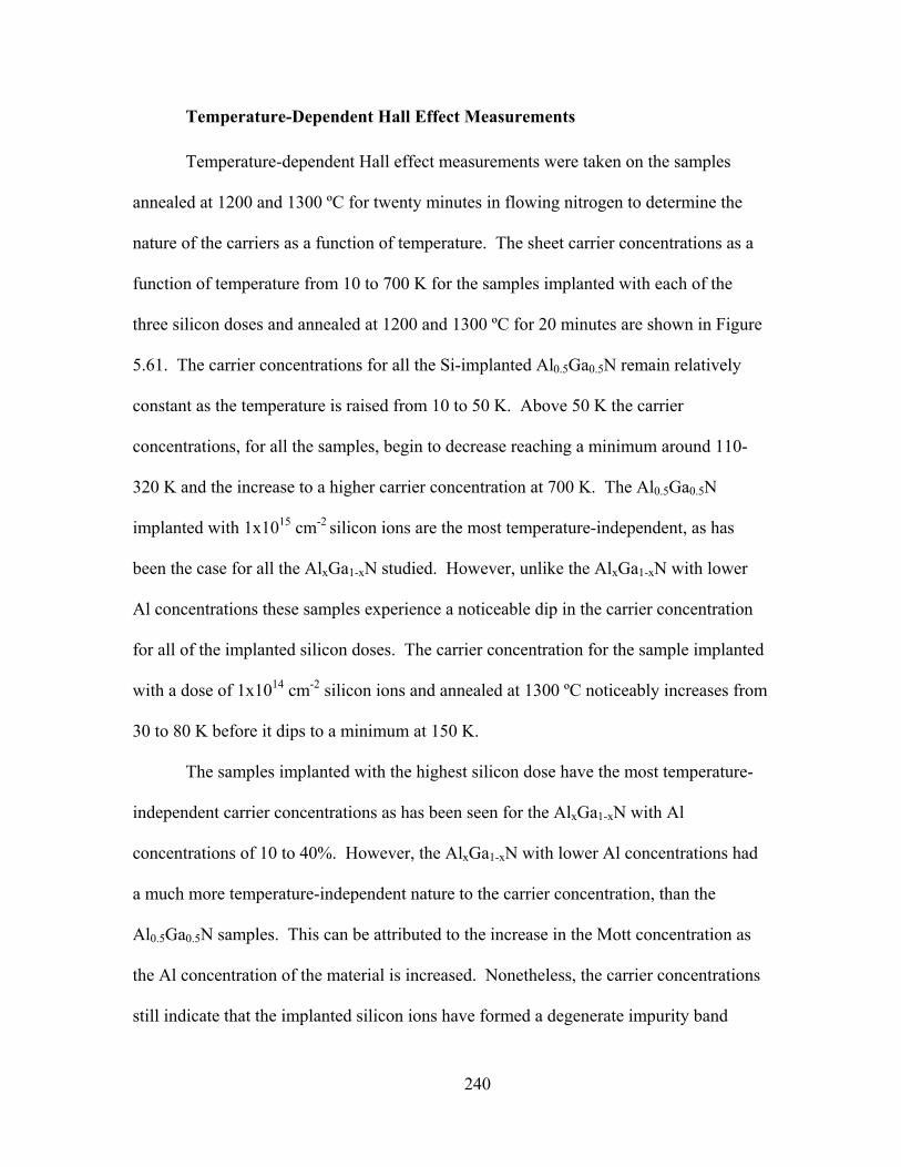
240
Temperature-Dependent Hall Effect Measurements
Temperature-dependent Hall effect measurements were taken on the samples
annealed at 1200 and 1300 ºC for twenty minutes in flowing nitrogen to determine the
nature of the carriers as a function of temperature. The sheet carrier concentrations as a
function of temperature from 10 to 700 K for the samples implanted with each of the
three silicon doses and annealed at 1200 and 1300 ºC for 20 minutes are shown in Figure
5.61. The carrier concentrations for all the Si-implanted Al0.5Ga0.5N remain relatively
constant as the temperature is raised from 10 to 50 K. Above 50 K the carrier
concentrations, for all the samples, begin to decrease reaching a minimum around 110-
320 K and the increase to a higher carrier concentration at 700 K. The Al0.5Ga0.5N
implanted with 1x1015 cm-2 silicon ions are the most temperature-independent, as has
been the case for all the AlxGa1-xN studied. However, unlike the AlxGa1-xN with lower
Al concentrations these samples experience a noticeable dip in the carrier concentration
for all of the implanted silicon doses. The carrier concentration for the sample implanted
with a dose of 1x1014 cm-2 silicon ions and annealed at 1300 ºC noticeably increases from
30 to 80 K before it dips to a minimum at 150 K.
The samples implanted with the highest silicon dose have the most temperature-
independent carrier concentrations as has been seen for the AlxGa1-xN with Al
concentrations of 10 to 40%. However, the AlxGa1-xN with lower Al concentrations had
a much more temperature-independent nature to the carrier concentration, than the
Al0.5Ga0.5N samples. This can be attributed to the increase in the Mott concentration as
the Al concentration of the material is increased. Nonetheless, the carrier concentrations
still indicate that the implanted silicon ions have formed a degenerate impurity band

0 20 40 60 80 100
1014
Temperature (K)
Al0.5Ga0.5N:SitA = 20 minutes
1x1015 cm-2
1200 oC 1300 oC
5x1014 cm-2
1200 oC 1300 oC
1x1014 cm-2
1200 oC 1300 oC
1000/T (K-1)
Shee
t Car
rier C
once
ntra
tion
(cm
-2)
700 100 50 25 20 15 10
Figure 5.61. Temperature-dependent sheet carrier concentrations of Al0.5Ga0.5N determined from Hall effect measurements taken from 10 to 700 K. The Al0.5Ga0.5N was implanted with three different doses of Si ions at 200 keV and annealed at 1200 and 1300 ºC for 20 minutes in a flowing nitrogen environment.
241

242
region in the band gap. All three of the implanted silicon doses in Al0.5Ga0.5N correspond
to volume carrier concentrations that exceed the Mott concentration. Like the AlxGa1-xN
with lower Al mole fractions, the samples implanted with 1x1014 cm-2 silicon ions exhibit
properties most like that of a non-degenerate semiconductor. The dip in carrier
concentrations of the Si-implanted Al0.5Ga0.5N signifies the presence of a multi-channel
conduction band, caused by the Gaussian profile of the implanted silicon ions (37,68).
Degenerate samples yield ionization energies lower than the actual energy due to
impurity screening. Impurity screening acts reduce the donor ionization energy and its
effects are enhanced by an increase in the concentration of ionized donors. Therefore, the
silicon ionization energy for Al0.5Ga0.5N can not be accurately estimated from the
samples in this study. However, Hwang et al. calculated from a simple hydrogen model
that the ionization for Al0.5Ga0.5N would be on the order of 61 meV.
The temperature-dependent Hall mobilities the Si-implanted Al0.5Ga0.5N are
shown in Figure 5.62. All of the samples exhibit a peak in their mobility curve around
320 K. The sample implanted with 1x1014 cm-2 silicon ions and annealed at 1300 ºC has
the highest mobility of 52 cm2/V·s after being annealed at 1300 ºC. The mobility of the
samples implanted with this dose and annealed at 1200ºC are considerably lower. Only
the samples implanted with the lowest silicon dose have higher mobilities for the samples
annealed at 1300ºC, which is consistent with the room temperature data. The mobility
curves become more temperature-independent as the implanted silicon dose is increased.
The samples implanted with 5x10¹⁴ and 1x1015 cm-2 silicon ions have very similar
temperature dependencies, especially in the high temperature regime. The peak
mobilities for the samples implanted with 5x1014 cm-2 silicon ions are 27 and 31 cm2/V·s
after being annealed at 1200 and 1300ºC, respectively. The samples implanted with the

0 100 200 300 400 500 600 700
0
10
20
30
40
50
Temperature (K)
1x1014 cm-2
1200 oC 1300 oC
5x1014 cm-2
1200 oC 1300 oC
1x1015 cm-2
1200 oC 1300 oC
Al0.5Ga0.5N:SitA = 20 minutes
Mob
ility
(cm
2 /V.s
)
Figure 5.62. Temperature-dependent mobilities calculated from Hall effect measurements taken from 10 to 700 K for Al0.5Ga0.5N implanted at room temperature with Si ions at 200 keV in three different doses and annealed at 1200 and 1300 ºC for 20 minutes.
243

244
highest silicon dose have peak mobilities of 27 and 35 cm2/V·s for the two anneal
temperatures, respectively. As seen in the AlxGa1-xN with lower Al concentrations, the
mobilities at 10 K increase as the implanted silicon is increased due to the degeneracy of
the samples. The mobilities at 10 K for the samples implanted with 1x10¹⁴, 5x10¹⁴, and
1x1015 cm-2 silicon ions and annealed at 1200 ºC are 4, 15, and 18 cm2/V·s. The mobility
for the samples that were annealed at 1300 ºC are 9, 23, and 28 cm2/V·s for the three
doses, respectively. The degenerate impurity region causes the low temperature mobility
to be temperature-independent, more so for the samples implanted with 1x1015 cm-2
silicon ions. The temperature-dependent mobility of the samples implanted with 1x10¹⁴
cm-2 silicon ions most resembles that which is predicted for a non-degenerate sample,
more so for the Al0.5Ga0.5N than the AlxGa1-xN with lower Al mole fractions due to the
increase in the Mott concentration as the Al mole fraction is increased. The mobility
curves for the Al0.1Ga0.9N and Al0.2Ga0.8N implanted with the higher silicon doses curves
are more flat and temperature-independent than they are for the Al0.5Ga0.5N. Also, the
lower Al mole fraction material had mobilities that clearly increased as the implanted
silicon dose was decreased, which is not the case here. The samples implanted with
5x10¹⁴ and 1x1015 cm-2 silicon ions and annealed at 1200 and 1300 ºC have higher
mobilities than the samples implanted with 1x1014 cm-2 silicon ions and annealed at 1200
ºC.
Figure 5.63 shows the temperature-dependent resistivity of the Al0.5Ga0.5N
samples annealed at 1200 and 1300 ºC for all three of the implanted silicon doses. The
samples annealed at the higher temperature of 1300 ºC had larger resistivity, except for
the samples that were implanted with a dose of 1x1015 cm-2 silicon ions which is
consistent with the room temperature data. The resistivity decreases significantly as the

0 20 40 60 80 100
200
400
600
800
1000
1200
1400
5000
Temperature (K)
Sh
eet R
esis
tivity
(Ω/s
q.)
1000/T (K-1)
1x1014 cm-2
1200 oC 1300 oC
5x1014 cm-2
1200 oC 1300 oC
1x1015 cm-2
1200 oC 1300 oC
Al0.5Ga0.5N:SitA = 20 minutes
700 100 50 25 20 15 10
Figure 5.63. Temperature-dependent resistivity calculated from Hall effect measurements taken from 10 to 700 K for Al0.5Ga0.5N that had been implanted at room temperature with silicon ions at 200 keV in does of 1x10¹⁴, 5x10¹⁴, and 1x1015 cm-2 and annealed at 1200 and 1300ºC for 20 minutes in flowing nitrogen.
245

246
implantation dose is increased and also becomes more temperature-independent. The Si-
implanted Al0.5Ga0.5N show a relative temperature-independent resistivity from 10 to 50
K and then the resistivity slowly dips to a minimum around 380 K before beginning to
increasing up through 700 K. The dip in the samples implanted with 1x1014 cm-2 silicon
ions is the most exaggerated and the drop resistivity for the samples implanted with
1x1015 cm-2 silicon ions is significantly less noticeable. This dip in the resistivity is
related to the dramatic increase in the carrier concentration and also the decline of the
mobility.
Low Temperature Cathodoluminescence Measurements
Cathodoluminescence measurements were taken at an electron energy of 10 keV
with 50 µA of source current, the temperature in the chamber was 7.4 K, and the slits on
the spectrometer were 400 µm both at the entrance and the exit. The range scanned was
1800 to 7000 Å with a step size of 2 Å and an integration time of 0.1 second.
The spectrum of the unimplanted samples shown as a function of anneal
temperature are given in Figure 5.64. To gauge the level of damage recovery in the
implanted samples the behavior of the unimplanted samples must first be observed. The
CL spectra for the as-grown sample shows a neutral-donor-bound exciton (Do,X) peak at
4.59 eV followed by three peaks at 4.49, 4.42, and 4.35 eV due to etalon effects. The
peak at 4.35 eV is more enhanced in the spectra of the implanted samples that it is for the
as-grown samples. The spectrum also has a broad luminescence centered at 3.0 eV,
similar to that seen in GaN, due to a deep impurity transition between a shallow donor
and a deep acceptor. Nam et al. observed that as the peak positions in AlxGa1-xN blue
shifted from 3.42 to 5.96 eV with increasing Al mole fraction from zero to one, the deep
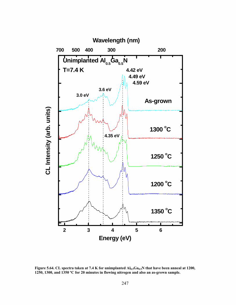
2 3 4 5 6
3.0 eV
Wavelength (nm)
3.6 eV
4.35 eV
4.42 eV4.49 eV
C
L In
tens
ity (a
rb. u
nits
)
Energy (eV)
Unimplanted Al0.5Ga0.5NT=7.4 K
1300 oC
1200 oC
1350 oC
1250 oC
As-grown
4.59 eV
700 500 400 300 200
Figure 5.64. CL spectra taken at 7.4 K for unimplanted Al0.5Ga0.5N that have been anneal at 1200, 1250, 1300, and 1350 ºC for 20 minutes in flowing nitrogen and also an as-grown sample.
247

248
impurity peaks also shifted from 2.15 eV (YL) in GaN to 3.90 eV (VL) for AlN (44).
They attribute this luminescence to be related to an Al vacancy or an Al vacancy
complex. The CL spectra also exhibit a broad luminescence centered around 3.6 eV that
is the most prominent in the spectrum of the as-grown sample. The origin of this
luminescence is unknown at this time but is most likely related to defects is the crystal
caused from the large incorporation of Al atoms. The as-grown sample has the most
intense (Do,X) peak. As the anneal temperature is increased from 1200 to 1300 ºC, the
intensity of the (Do,X) peak increases however, annealing at 1350 ºC severely decreases
the intensity of the (Do,X) peak, most likely due to annealing related damage. The
implanted samples show considerable amplification of the 3.0 eV and diminishing
intensity of the 3.6 eV band compared to that of the as-grown sample. As the anneal
temperature is increased from 1200 to 1300 ºC the 3.0 eV band intensifies and the peaks
become more distinguished.
The low temperature CL spectra for the Si-implanted Al0.5Ga0.5N annealed for 20
minutes at 1250 ºC are shown in Figure 5.65. All of the samples have a comparable
spectrum with the unimplanted sample. The spectrum show a (Do,X) peak at 4.59 eV
followed by a several other peaks due to etalon effects. All of the spectra have a
dominant luminescence centered at 3.0 eV that is attributed to deep impurity transitions
most likely related to Al vacancy complexes (44). There is also an unknown
luminescence centered at 3.6 eV that could be the result of as-grown defects from the Al
composition of the sample. All of the spectra of the implanted Al0.5Ga0.5N show an
increase in the 3.0 eV band compared to the as-grown sample, with samples implanted
with 1x1014 cm-2 silicon ions being the most profound. The unimplanted samples have
the weakest intensity. The intensity of the spectra decrease as the implanted dose is

2 3 4 5 6
4.24 eV4.59 eV
3.0 eV
Wavelength (nm)
4.34 eV
C
L In
tens
ity (a
rb. u
nits
)
Energy (eV)
1x1014 cm-2
Unimplanted
1x1015 cm-2
5x1014 cm-2
Si-implanted Al0.5Ga0.5N
Anneal: 1250oC/ 20 min.T=7.4 K
3.6 eV
4.42 eV
4.49 eV
700 500 400 300 200
Figure 5.65. CL spectra taken at 7.4 K for Si-implanted Al0.5Ga0.5N that have been anneal at 1250 ºC for 20 minutes in flowing nitrogen.
249
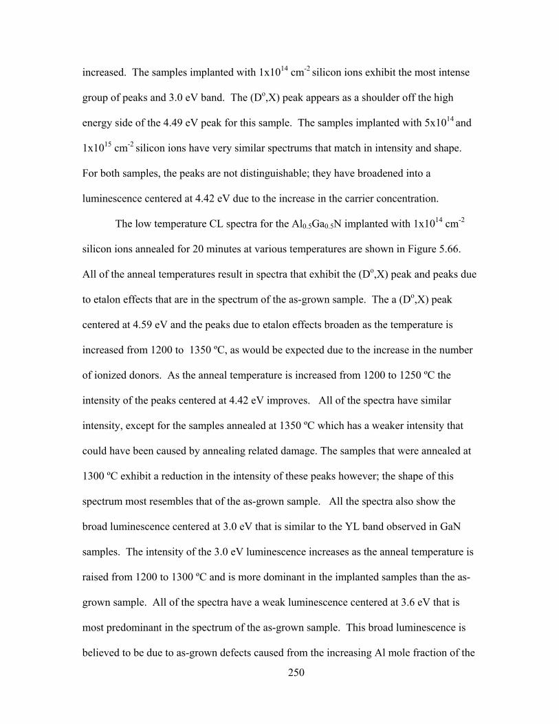
250
increased. The samples implanted with 1x1014 cm-2 silicon ions exhibit the most intense
group of peaks and 3.0 eV band. The (Do,X) peak appears as a shoulder off the high
energy side of the 4.49 eV peak for this sample. The samples implanted with 5x10¹⁴ and
1x1015 cm-2 silicon ions have very similar spectrums that match in intensity and shape.
For both samples, the peaks are not distinguishable; they have broadened into a
luminescence centered at 4.42 eV due to the increase in the carrier concentration.
The low temperature CL spectra for the Al0.5Ga0.5N implanted with 1x1014 cm-2
silicon ions annealed for 20 minutes at various temperatures are shown in Figure 5.66.
All of the anneal temperatures result in spectra that exhibit the (Do,X) peak and peaks due
to etalon effects that are in the spectrum of the as-grown sample. The a (Do,X) peak
centered at 4.59 eV and the peaks due to etalon effects broaden as the temperature is
increased from 1200 to 1350 ºC, as would be expected due to the increase in the number
of ionized donors. As the anneal temperature is increased from 1200 to 1250 ºC the
intensity of the peaks centered at 4.42 eV improves. All of the spectra have similar
intensity, except for the samples annealed at 1350 ºC which has a weaker intensity that
could have been caused by annealing related damage. The samples that were annealed at
1300 ºC exhibit a reduction in the intensity of these peaks however; the shape of this
spectrum most resembles that of the as-grown sample. All the spectra also show the
broad luminescence centered at 3.0 eV that is similar to the YL band observed in GaN
samples. The intensity of the 3.0 eV luminescence increases as the anneal temperature is
raised from 1200 to 1300 ºC and is more dominant in the implanted samples than the as-
grown sample. All of the spectra have a weak luminescence centered at 3.6 eV that is
most predominant in the spectrum of the as-grown sample. This broad luminescence is
believed to be due to as-grown defects caused from the increasing Al mole fraction of the

2 3 4 5 6
4.24 eV
3.0 eV
Wavelength (nm)
4.59 eV
4.34 eV
3.6 eV
Si-implanted Al0.5Ga0.5N
1x1014cm-2
T=7.4 K
1350 oC
1200 oC
1250 oC
1300 oC
As-grown
C
L In
tens
ity (a
rb. u
nits
)
Energy (eV)
4.42 eV
4.49 eV
700 500 400 300 200
Figure 5.66. CL spectra taken at 7.4 K for Al0.5Ga05N that has been implanted with 1x1014 cm-2 silicon ions and annealed at various temperatures for 20 minutes in flowing nitrogen.
251

252
material. The intensity of the 3.6 eV band for the samples annealed at 1200 and 1250 ºC
remains the same as that of the as-grown sample. The intensity of this band deceases as
the anneal temperature is increased up to 1350 ºC, indicating that an anneal temperatures
of at least 1300 ºC are required to repair as-grown defects in Al0.5Ga0.5N.
The CL spectra of the samples implanted with a silicon dose of 5x1014 cm-2
silicon ions and annealed for 20 minutes at various temperatures are shown in Figure
5.67. All of the anneal temperatures result in spectra that exhibit the (Do,X) peak and
etalon effects that are in the spectrum of the as-grown sample. However, the (Do,X) peak
an phonon replicas are not as distinguishable for the implanted samples as they are for the
as-grown sample. The a (Do,X) peak centered at 4.59 eV and the etalon effect peaks
broaden as the temperature is increased from 1200 to 1300 ºC, as would be expected due
to the increase in the number of ionized donors. Initially, the intensity of these peaks
increases as the anneal temperature is raised from 1200 to 1250 ºC, however increasing
the anneal temperature further causes the intensity to diminish. All of the spectrums for
the implanted samples have a dominant broad luminescence centered at 3.0 eV, which is
enhanced compared to the as-grown sample, which is similar to the YL band observed in
GaN samples (44). The 3.0 eV band for the sample annealed at 1250 ºC is orders of
magnitude higher than that of the samples annealed at the other temperatures. The
intensity of this band decreases for higher anneal temperature. All of the spectra have a
weak luminescence centered at 3.6 eV that is most predominant in the spectrum of the as-
grown sample. This broad luminescence is believed to be due to as-grown defects caused
from the increasing Al mole fraction of the material. The intensity of the 3.6 eV band for
the samples annealed at 1200 and 1300 ºC remains the same as that of the as-grown
sample. The intensity of this band increases only for the sample annealed at 1250 ºC.
2 3 4 5 6
3.0 eV
Wavelength (nm)
As-grown
C
L In
tens
ity (a
rb. u
nits
)
Energy (eV)
Si-implanted Al0.5Ga0.5N
5x1014cm-2
T=7.4 K
1200 oC
1300 oC
1250 oC
1350 oC
3.6 eV4.42 eV
4.49 eV4.59 eV
700 500 400 300 200
Figure 5.67. CL spectra taken at 7.4 K for Al0.5Ga0.5N that has been implanted with 5x1014 cm-2 silicon ions and annealed at various temperatures for 20 minutes in flowing nitrogen.
253

254
The intensity of this band deceases as the anneal temperature is increased to 1350 ºC,
indicating that an anneal temperatures of at least 1350 ºC are required to repair as-grown
defects in Al0.5Ga0.5N. The electrical results for samples implanted with this silicon dose
all steadily improve as the anneal temperature was increased from 1200 to 1300 ºC,
which corresponds to a decrease of the 3.0 eV luminescence.
The CL spectra of the samples implanted with a dose of 1x1015 cm-2 silicon ions
and annealed for 20 minutes at various temperatures are shown in Figure 5.68. All of the
anneal temperatures result in spectra that exhibit the (Do,X) peak and etalon effects that
are in the spectrum of the as-grown sample. However, the (Do,X) peak an phonon
replicas are not as distinguishable for the implanted samples as they are for the as-grown
sample. The a (Do,X) peak centered at 4.59 eV and the etalon effect peaks broaden as the
temperature is increased from 1200 to 1300 ºC, as would be expected due to the increase
in the number of ionized donors. The spectra for the sample annealed at 1250 ºC had to
be reduced by a factor of 5. The intensity of the (Do,X) peak decreases as the anneal
temperature is increased from 1200 to 1300 ºC and is no longer observable in the
spectrum of the sample annealed at 1350 ºC. All of the spectrums for the implanted
samples have a dominant broad luminescence centered at 3.0 eV, similar to the YL band
observed in GaN samples, which is enhanced compared to the as-grown sample (44).
The 3.0 eV band is not the dominant feature in the spectrum of the samples annealed at
1350 ºC, but rather the main feature is a luminescence centered around 2.5 eV. This band
is present in all the spectra of the Si-implanted samples. Nam et al. also observed a
luminescence band at 2.56 eV that was only observed in samples with Al mole fraction
greater than 0.5, and increased as the Al mole fraction was increased (44). They
attributed this impurity band to a DAP transition from shallow donor to an aluminum

2 3 4 5 6
3.6 eV
Wavelength (nm)
2.5 eV
4.49 eV
x1/5
As-grown
C
L In
tens
ity (a
rb. u
nits
)
Energy (eV)
Si-implanted Al0.5Ga0.5N
1x1015cm-2
T=7.4 K
1300 oC
1250 oC
1200 oC
1350 oC
3.0 eV
4.42 eV
4.59 eV
700 500 400 300 200
Figure 5.68. CL spectra taken at 7.4 K for Al0.5Ga0.5N that has been implanted with 1x1015 cm-2 silicon ions and annealed at various temperatures for 20 minutes in flowing nitrogen.
255

256
vacancy (VAl)3-, which acts as a deep acceptor. This luminescence was not observed in
the Al0.5Ga0.5N implanted with lower silicon doses or in the as-grown sample All of the
spectra have a weak luminescence centered at 3.6 eV that is most predominant in the
spectrum of the as-grown sample, except for the sample annealed at 1350 ºC. This broad
luminescence is believed to be due to as-grown defects caused from the increasing Al
mole fraction of the material. The 3.36 eV luminescence band decreases for all of the
anneal temperatures, except for the samples annealed 1250 ºC for which it is considerably
enhanced. The 3.36 eV band is not present in the spectra for the sample annealed at
1350 ºC, similar to the behavior of the Al0.5Ga0.5N implanted with the lower silicon
doses. The spectrum for the sample annealed at 1350 ºC has a different shape than the
other spectra, as was seen in the Al0.4Ga0.6N samples implanted with all three doses and
annealed at this temperature.
Summary
The Si-implanted AlxGa1-xN samples with Al mole fractions from 10 to 50% all
achieved high activation efficiencies after a high temperature anneal treatment. The
highest obtainable activation for each implanted sample are shown in Table 5.5 along
with the anneal conditions and other physical properties.
Anneal conditions were determined for each Al mole fraction implanted with each
silicon dose that produce greater than 95% activation in most samples. The activations
and mobilities obtained for Si-implanted AlxGa1-xN, in this study, are higher than those
reported (33-35, 47, 51-52).

257
Table 5.5. The electrical results obtained for the annealing conditions that produced the highest electrical activation efficiency for each silicon dose implanted into AlxGa1-xN.
Silicon dose
(cm-2)
Anneal Temp.
(ºC)
Anneal Time (min.)
Activation (%)
Carrier Concentration
(cm-2)
Mobility (cm2/V·s)
Resistivity (Ω/)
1x10¹⁴ 1200 40 73 7.13x10¹³ 101 792
Al0.1Ga0.9N 5x10¹⁴ 1200 40 94 4.61 x10¹⁴ 70 190
1x10¹⁵ 1200 40 100 9.95 x10¹⁴ 64 96
1x10¹⁴ 1300 20 83 8.25 x10¹³ 76 1000
Al0.2Ga0.8N 5x10¹⁴ 1300 20 100 5.33 x10¹⁴ 54 214
1x10¹⁵ 1300 20 100 9.92 x10¹⁴ 54 115
1x10¹⁴ 1300 20 74 7.27 x10¹³ 80 1298
Al0.3Ga0.7N 5x10¹⁴ 1300 1350
20 20
88 90
4.34x10¹⁴
4.49 x10¹⁴ 58 64
249 221
1x10¹⁵ 1200 1300
40 20
100 100
1.00 x10¹⁴
1.00 x10¹⁴ 47 61
121 95
1x10¹⁴ 1350 20 99 9.78x10¹³ 58 1099
Al0.4Ga0.6N 5x10¹⁴ 1200 40 100 5.02x10¹⁴ 38 316
1x10¹⁵ 1200 40 96 9.56x10¹⁴ 41 159
1x10¹⁴ 1300 20 100 9.98x10¹³ 51 1223
Al0.5Ga0.5N 5x10¹⁴ 1300 20 96 4.78x10¹⁴ 36 362
1x10¹⁵ 1300 20 66 6.59x10¹⁴ 35 270

VI. Conclusions
Ion implantation of silicon ions into AlxGa1-xN with Al mole fractions of 0.1 to
0.5 was found to be a viable method of creating highly conductive n-type material. The
implanted silicon ions were readily activated with a post implantation annealing
treatment that resulted in a minimum of 66% activation efficiency of the implanted ions
and in most cases close to 100% activation. The optimal annealing temperature was
found to vary between 1200 and 1350 °C depending on the anneal time, ion dose, and Al
mole fraction of the sample. The overall mobilities are weak in comparison to Si or
GaAs; however they are higher than those reported in the literature for Si-implanted
AlxGa1-xN (33-35, 47, 51-52). Resistivity values lower then 100 Ω/ were attainable.
The Si-implanted AlxGa1-xN with Al concentrations of 10 to 30% were found to
behave similarly to each other as well as GaN in that the higher implanted silicon doses
are more readily activated than the lower implanted doses. As the Al mole fraction of the
AlxGa1-xN was increased up to 50% the trend reverses and higher activations are achieved
for the samples implanted with the lower silicon doses, as is the case with gallium
arsenide (GaAs). However, the Al0.4Ga0.6N exhibit much less of a preference on the
doping level and high activation efficiencies were achieved for all three silicon implanted
doses. This phenomenon could be related to the elevated temperatures required to
sufficiently repair lattice damage in the higher Al mole fraction material.
The annealing conditions for the implanted AlxGa1-xN were varied in order to
attain the best configuration of time and temperature that generates the highest activation
of the implanted silicon ions as well as significant restoration of the crystal lattice
configuration. The anneal temperature at which the majority of the ion implantation
258

induced lattice damage is repaired was found to increase as the Al mole fraction of the
material was increased indicating that damage profile from the implantation increased as
the Al mole fraction increased. Correlating the activation efficiency and mobility data for
the Al0.1Ga0.9N samples indicated that most of the lattice damage had been recovered
after annealing at 1200°C, while this did not occur for the Al0.2Ga0.8N samples until after
annealing at 1250°C. Complete lattice recovery did not take place for the AlxGa1-xN with
higher Al mole fractions even after annealing at temperatures up to 1350°C. However,
electrical activations of the implanted silicon were greater than 95% for most of the
implanted doses.
The optimal annealing temperature for the AlxGa1-xN with Al concentrations of 10
to 30% increases as the implanted silicon dose is decreased or the Al concentration of the
material is increased. Optimal annealing conditions are easily identified for the samples
implanted with a dose of 1x1015 cm-2 silicon ions however; the samples implanted with
the lower silicon doses do not always achieve 100% activation. The Al0.1Ga0.9N required
the lowest temperatures to activate the implanted ions and therefore responded the best to
a lengthened anneal time of 40 minutes at an anneal temperature of 1200 ºC. These are
the annealing conditions for Al0.1Ga0.9N and produce electrical activation efficiencies of
73, 94, and 100% for the Al0.1Ga0.9N implanted with doses of 1x10¹⁴, 5x10¹⁴, and 1x10¹⁵
cm-2 silicon ions, respectively. For the Si-implanted Al0.2Ga0.8N the optimal annealing
conditions are 1300 ºC for 20 minutes, which generate electrical activation efficiencies of
100% for the samples implanted with the two higher silicon doses. The Al0.2Ga0.8N
implanted with the lowest silicon dose had an electrical activation of only 83%, even
after annealing at 1300 ºC. An anneal temperature of 1300 ºC produced excellent
259

activation for the Si-implanted Al0.2Ga0.8N however, this anneal temperature was not high
enough to produce the same results for the Al0.3Ga0.7N samples. This anneal temperature
generated electrical activation efficiencies of 74, 88, and 100% for Al0.3Ga0.7N implanted
with doses of 1x10¹⁴, 5x10¹⁴, and 1x1015 cm-2 silicon ions, respectively. The electrical
activations for the two lower implanted silicon doses for the Al0.3Ga0.7N are much lower
than those of the Al0.2Ga0.8N, indicating that a higher anneal temperature or longer anneal
time may be required to achieve improved activation for these samples. Samples with all
three Al mole fractions have their lowest electrical activations for the samples implanted
with 1x1014 cm-2 silicon ions. These samples show no sign of saturation suggesting that
higher anneal temperatures or longer anneal times may produce elevated activation
efficiencies. The annealing conditions were found to be dependent on the implanted
silicon dose as well as the Al concentration of the material, with lower doses and higher
Al mole fractions requiring higher annealing temperatures.
The Si-implanted AlxGa1-xN with Al concentrations of 40 and 50% shifts in
behavior from that of the samples with lower Al concentrations, in that the lower silicon
implanted doses are more readily activated. Although the Al0.4Ga0.6N exhibits a high
activation efficiency for the lowest implanted silicon dose, the anneal conditions are
much more extreme (1350 ºC for 20 minutes) than those required to achieve 100 and 96%
electrical activation for the two higher silicon implanted doses. The latter two activations
were obtained after annealing the Al0.4Ga0.6N implanted with doses of 5x10¹⁴ and 1x10¹⁵
cm-2 silicon ions at 1200 ºC for 40 minutes. By increasing the Al concentration to 40%
the samples maintain the ability to readily activate the high dose implants and gain the
ability to activate low doses as well. The Al0.5Ga0.5N behaves as the Al0.4Ga0.6N samples
260

however, the increase in Al content caused the materials ability to activate highest dose
implants to diminish. Electrical activation efficiencies of 100 and 96% were obtained
after annealing the Al0.5Ga0.5N implanted with doses of 1x10¹⁴ and 5x1014 cm-2 silicon
ions for 20 minutes at 1300 ºC. The Al0.5Ga0.5N implanted with a dose of 1x1015 cm-2 has
an electrical activation of only 66% after being annealed at the same conditions.
Optimal annealing conditions were identified for the Si-implanted AlxGa1-xN as a
function of implanted silicon dose and Al concentration. Based on the electrical
activations the optimum annealing conditions appear to be 1200 ºC for 40 minutes or
1300 ºC for 20 minutes and dependent on the implantation dose and the Al mole fraction
of the material. The AlxGa1-xN with Al concentrations of 10 and 40% implanted with
doses of 5x10¹⁴ and 1x1015 cm-2 silicon ions manifest their best electrical properties after
being annealed for 40 minutes at 1200 ºC, while the remaining Al concentrations
preferred the higher temperature anneal. The Al0.4Ga0.6N is the transition point between
the activation behavior of the lower Al concentration samples and that of the Al0.5Ga0.5N,
allowing for easy activation of al three implanted silicon doses.
The electrical activation efficiencies obtained for the AlxGa1-xN with Al mole
fractions from 0.1 to 0.5 are higher than those reported in similar studies for all of the Al
mole fractions investigated (32-36, 47-48, and 51-53). At least one dose had an
activation of 100% for each Al mole fraction and in most cases each Al mole fraction had
samples that had an activation efficiency around 95% for a second dose. The high
activations were obtained at relatively low annealing temperatures of 1200 and 1300 ºC.
The Si-implanted AlxGa1-xN also had higher mobilities and lower resistivity than those in
the aforementioned reports.
261

The electrical properties obtained from Hall Effect measurements, such as the
carrier concentration, mobility and resistivity of the implanted silicon all change as a
function of the Al concentration of the material. Graphs of these properties as a function
of Al mole fraction can be found in Appendix B. In general, these properties all decrease
as the implanted silicon dose is increased. However, increasing the Al content of the
AlxGa1-xN has differing effects on the mobility and the resistivity.
In general, the mobility increased as the anneal temperature was increased from
1100 to 1350 ºC. The mobility decreases as the Al mole fraction of the material is
increased which is most likely due to the increase in the effective mass as the Al
concentration is increased. The mobility also decreases as the implanted silicon dose is
increased due to an increase in ionized impurity scattering. All of the Al mole fractions
investigated exhibited an increase in mobility despite an increase in the activation
indicating that a decrease in defect scattering has stronger effects on the mobility than an
increase in impurity scattering. The AlxGa1-xN for all the Al mole fractions exhibited the
highest mobility for the samples implanted with a dose of 1x1014 cm-2 silicon ions. The
highest mobility obtained at 300 K was 109 cm2/V·s for an Al0.1Ga0.9N sample that had
been implanted with 1x1014 cm-2 silicon ions and annealed at 1200 ºC for 20 minutes in
nitrogen ambient. This is the highest reported mobility for Si-implanted Al0.1Ga0.9N
however; the mobility is much lower than those observed in Si-implanted GaN (22). The
peak mobility for the Al0.5Ga0.5N implanted with a silicon dose of 1x1015 cm-2 is the
lowest of all the samples at 35 cm2/V·s after being annealed for 20 minutes at 1350 ºC.
The mobility values obtained in this study are higher than those reported in the literature
262
for samples with similar Al compositions and implantation conditions, except for the
20% samples where Ryu et al. obtained slightly higher mobilities (35).
The resistivity for all the implanted samples decreases as the ion dose is decreased
or as anneal temperature is increased from 1100 to 1350 ºC due to an increase in lattice
damage recovery and in activation efficiency. The lowest resistivity obtained was 96
Ω/, for an Al0.1Ga0.9N sample that was implanted with 1x1015 cm-2 silicon ions and
annealed at 1200 ºC for 40 minutes. The resistivities for the AlxGa1-xN samples
implanted with the highest silicon dose are under 270 Ω/, while the samples implanted
with 5x1014 cm-2 silicon ions have resistivities under 362 Ω/. The resistivity of the
AlxGa1-xN samples implanted with a dose of 1x1014 cm-2 silicon ions are much larger,
increasing from 792 to 1298 Ω/ as the Al composition is increased from 10 to 30%,
where it reaches a maximum. As the Al concentration is increased to 40% the resistivity
declines to 1099 Ω/ however, it increases again as the Al concentration is raised to 50%.
The temperature-dependent Hall shows that the samples are degenerate. The
AlxGa1-xN samples implanted with a dose of 1x1014 cm-2 silicon ions exhibit less of a
temperature-independence than the samples implanted with the higher silicon doses. The
Mott concentration for AlxGa1-xN increases slightly as the Al mole fraction is increased,
so that as the Al mole fraction is increased from 0.1 to 0.5 the samples implanted with the
lower silicon doses become more temperature-dependent.
All the CL spectra for the Si-implanted AlxGa1-xN have a dominant donor bound
exciton peak whose energy shifts from 3.7 to 4.6 eV has the Al mole fraction is increased
form 0.1 to 0.5. The implanted Al0.1Ga0.9N samples have a broad yellow luminescence
(YL) band centered around 2.4 eV, which is not visible for the Al0.2Ga0.8N. This broad
263

luminescence shifts to 3.6 eV for the Al0.3Ga0.7N and is only visible for the samples
implanted with 1x10¹⁴ and 1x1015 cm-2 silicon ions that were annealed at 1200 °C. The
Al0.4Ga0.6N samples have a very weak luminescence around 2.8 eV for the higher
implanted silicon doses. The Al0.5Ga0.5N samples have a large luminescence centered
around 3.1 eV that is more intense than the donor bound exciton peak. The broad band
luminescence is attributed to a transition between silicon donors and a deep acceptor that
could possibly be an aluminum vacancy or aluminum vacancy complex (44).
The mobility, resistivity and the high electrical activations achieved in this study
for the implanted AlxGa1-xN, when correlated with the temperature-dependent and
cathodoluminescence data, conclude that AlxGa1-xN is a well suited material for
electronic and optical device applications. The fundamental properties can easily be
modified with Si-implantation to create the desired material functionality required for
different device purposes. This research will assist device engineers by offering
enhanced insight into the silicon activation of implanted AlxGa1-xN that will improve the
performance of AlxGa1-xN based devices that require ion implantation.
264
265
Recommendations for Future Research
1. Replace the AlN encapsulant. As the Al mole fraction of the material is
increased the AlN capping layer becomes more difficult to remove.
2. Investigate the optical properties of the material with temperature and power
dependant cathodoluminescence to determine the nature of broad luminescence
features and their connection to the activation efficiency.
3. Anneal the Al0.1Ga0.9N and Al0.2Ga0.8N implanted with doses of 5x10¹⁴ and
1x1015 cm-2 silicon ions at lower temperatures than 1200 ºC extending the anneal
time beyond 20 minutes to obtain significant electrical activation efficiencies.
4. Determine commercially viable annealing conditions for the AlxGa1-xN
implanted with a dose of 1x1014 cm-2 for Al concentrations of 10 to 30% and
Al0.5Ga0.5N implanted with a dose of 1x1015 cm-2 silicon ions.
5. Continue the investigation of Si-implanted AlxGa1-xN with Al mole fractions of
0.6 to 1.

Appendix A
Hall Effect Measurements
Room Temperature Measurements – Sample Mounting 1. Use the green sample card kept in the cabinet by the HT system. 2. Place sample within the outline square on card 3. Place one of the four pressure probes on each contact. 4. Use the curve tracer (power on, memory 1, hit recall) to check the connections 5. Insert card into RT sample mount. 6. Connect the 4 yellow testing cables to the top of the sample probe. Low Temperature Measurements – Sample Mounting 1. Turn on the soldering iron. 2. Get a wet paper towel from the restroom. 3. Use indium solder only. Place some on a glass slide. 4. The LT sample holder is brass with four gold wires kept in the drawer of the
LT system. Make sure the sapphire plate is in place. 5. Check the wires on the samples holder, spare wire is kept in the drawer to the
right of the desk. 6. Apply a small drop of rubber cement to the back of the sample using a
sharpened cotton swap stick. 7. Mount the sample in the middle of the sapphire plate. Wait a few minutes for
the rubber cement to dry. 8. With the soldering iron place a small amount of indium of each contact. 9. Attach the wires from the samples holder to the contacts on the sample. 10. Use the curve tracer to test the connection. 11. Place the samples holder on the samples mount and tighten in place with 2
screws. 12. Attached the cold shield with 2-4 brass screws 13. Attach the top cover so that the windows are opposite the windows of the cold
shield; tighten in place with 4 screws. 14. Connect the 4 yellow testing cables to the side of the sample chamber. 15. Check that the temperature sensor cable is connected. 16. Check that the vacuum gauge is connected. 17. Connect the turbo pump. 18. Turn the turbo pump on and let it come up to speed. 19. Open the valve so that the turbo pumps on the chamber. 20. Carefully flip the sample chamber in between the magnets, making sure the
helium lines do NOT rub against the mounting plate. 21. Wait for the chamber pressure to get below 10 microns. (~30 minutes) 22. Turn on water to the compressor. NEVER turn on water to full pressure,
open valve enough to override the interlocks of the compressor. 23. Turn on compressor and wait for system to cool. (~45 minutes)
266

High Temperature Measurements – Sample Mounting 1. Place high temperature head on foam block 2. Make sure set screws are loose so that the sample can fit underneath the
probes. 3. Place sample in the center of the copper sample holder. 4. Place one probe on a contact at a time by tightening the set screws. 5. Place the probes in a clockwise fashion careful not to knock the previous
probe out of position. 6. Use the curve tracer to test the connection. 7. Carefully place the sample holder into the vacuum jacket and secure with
clamp. 8. Connect the 4 yellow testing cables to the top of the sample chamber. 9. Connect the yellow thermocouple wire 10. Connect the heater cable. 24. Turn the turbo pump on and let it come up to speed. 11. Open the valve so that the turbo pumps on the chamber. 12. Wait for the chamber pressure to get below 10 microns. (~15 minutes) System Start-up 1. Turn on water to magnets. NEVER turn on water to full pressure, open valve
enough to override the interlocks of the magnets. 2. Checks to make sure the return water lines are open. 3. Check for water leaking from the connections at the back of the magnets. 4. Check the placement of the Gaussmeter. 5. Flip the switch on the front of the magnet power supply into stand by mode. 6. Make sure all the interlock lights are green. Hit the reset button if any are red. 7. Push the green button to power on the magnets. 8. Turn on equipment stack. (red button upper right side on cabinet) 9. Turn on the computer and log in with password Lake Shore. 10. Open the program from icon on desktop. (Hall Measurement System) 11. Make sure all equipment in functioning by checking the Systems Logs box in
the program. Taking Measurements 1. Choose a current to test the samples, one that works through the entire
temperature range. - Click on the resistivity button at the top right corner of the program. - Choose high or low resistivity. - Select the contact configuration to test (12,12). - Select a current and click the measure button. - Monitor that the out put is in range and that there are no errors. - Check that the current works for all contact pairs. (23,23; 34,34; 14,14)
2. Check that the contacts are linear.
267

268
- Do an I-V test with the selected current chose a step that results is about 5 measurement points. (right click in the measurements box on the left and choose I-V measurement) - Choose high or low resistivity based on the sample material. - Choose default contact pairs, click ok. - Click the Start button at the top of the program.
3. Create a program for RT, HT or LT measurements. (right click in the measurements box on the left and choose variable field of variable temperature measurement) - Select Hall and resistivity measurements - Select to calculate resistivity at zero field. - Select a magnetic field of 5 kG; choose a step of 1 kG. - Enter the chosen current both positive and negative. - Select high or low resistivity. - Enter the temperatures for measurement.
* Temperature-dependent measurements take ~5 hours. * Room temperature measurements with different three currents take ~20 min. Shut Down 1. Turn off the magnets. (red button) 2. Put the magnet power supply out of stand by mode. (toggle switch) 3. Turn off water to magnets. 4. Turn off compressor after LT measurements. 5. Turn of water to the compressor. 6. Close the HMS.exe program. 7. Turn off computer monitor or entire stack if not going to use for awhile. 8. Wait for systems to return to room temperature. (294 K) 9. Turn of vacuum pump. (ONLY if system is at room temperature) 10. Wait for sample chamber to pressurize. 11. Unplug the necessary cables to remove sample mount. 12. Remove sample. 13. Assemble the sample chamber to keep dust and contaminants out while not in
use.

Cathodoluminescence Measurements
Mounting Sample 1. Prepare, at most 8 samples, by thoroughly cleaning the surface in the clean
room with TCE, acetone, methanol, and DI water. 2. The sample holder is marked with a black line across the top and an “X” and a
black line on the bottom. Two samples can be mounted on at the top and 6 can be mounted on the bottom row beginning at the “X”. The samples mounted on the top (bottom) row should be mounted slightly above (below) the black line to unsure proper grounding.
3. Apply a small drop of rubber cement to the back of the sample using a sharpened cotton swap stick to the portion of the sample that will be placed above (below) the black line. Wait a few minutes for the rubber cement to dry.
4. There are 4 mounting screws inside the chamber. Make sure they are loose. 5. Slide the sample plated onto the 4 screws 6. Place the grounding bars on the screws and then tighten, making sure that the
grounding bar makes contact with all the samples. 7. Close chamber door 8. When mounting a whole 2 inch wafer, do not use sample holder. Take out he
4 mounting screws. Place flat edge of wafer up leaving one of the mounting screws holes uncovered. Use this mounting screw to mount pne discharge bar.
System Start-up 1. Open vacuum line is open. (green in-line valve on the floor under table) 2. Turn on roughing pump by flipping breaker on the wall. (2nd from right) 3. Check that power strips behind the computer are on. 4. Turn on power to turbo pump. 5. Turn on power to vacuum pressure moniter. 6. Plug the green switch on the back of the turbo pump. 7. Flip switch on small black box on the back of the table to begin pumping on
the chamber. (On is to the right) 8. When chamber pressure is less than 1x10⁻² (~10 minutes) turn on turbo pump.
(Press start un Alcatel box) 9. When chamber pressure reads 1x10⁻³, turn on ion gauge. (Green light comes
on) 10. Flip switch on black box to off. (towards the left) Cooling 1. Turn on water ( in-line valve on floor under table) 2. Turn on Lakeshore temperature controller. 3. Wait until chamber pressure is below 5x10⁻⁶.(~30 minutes) 4. Turn off ion gauge. 5. Check pressure reading on back of compressor.
269

270
6. Turn first switch on the right on the back of the compressor. Wait 10 seconds. 7. Flip the second switch. There is a 30 second built-in delay. 8. Flip the last switch to turn on the cold head. (It takes about one hour to cool) Taking Measurements 1. Turn the key on gamma high voltage supply. 2. Turn on E-gun power. (green button) 3. Turn on High voltage (red button) 4. Turn on Source (red button) 5. Turn on Deflection (blue button) 6. Turn the E-gun energy knob the desired energy. ( 10keV) 7. Make sure ammeter on top of the spectrometer is on. 8. Slowly turn up the E-beam source current to 2.3 - 2.5 Amps, until the
ammeter reads 50 µA. Takes ~30 minutes to stabilize. 9. Turn on PMT HV power supply. (push button, lower right) 10. Supply 1500 V to PMT (toggle switch, lower left) 11. Turn on computer and open the “Instrument Control” program. Select yes to
both questions. 12. Check the slit openings on the spectrometer. 13. Check to make sure the program is set up to read from the correct slit
openings. 14. Open the Faraday cup. Be gentle it is tricky. The current on the ammeter will
drop. 15. Focus the beam on the samples using the X-Y control box. 16. Turn off the room lights to eliminate background noise. 17. Align the sample luminescence with the entrance slit on the spectrometer
using two lenses. 18. Open shutter all the way. 19. Take spectrum. Shut Down 1. Gradually turn down source current on E-gun. 2. Turn down the E-gun energy. 3. Turn off all buttons, 2 red, green and blue. 4. Turn the key on the high voltage source. 5. Turn off high voltage to PMT. 6. Close the shutter on spectrometer. 7. Cover lenses. 8. Turn off computer monitor. 9. Turn off compressor – 3 switches from left to right. 10. Wait for chamber to reach 294 K. (~12 hours) 11. Stop the turbo pump. 12. Pull green plug from back of turbo. 13. Wait for the system to pressurize. (~30 minutes) 14. Turn off Turbo pump. 15. Turn off roughing pump. (flip breaker)

Appendix B
This Appendix contains graphs of the activation efficiency, mobility, resistivity
and donor bound exciton energy as a function of the Al mole fraction of the material to
aid in the discussion in the conclusion. The plot of the donor bound exciton peak energy
as a function of the Al mole fraction utilizes the calculated mole fractions from Equation
4.1, assuming a bowing parameter of one, that are given in Table 4.1. This is followed by
plots of the activation efficiency, mobility and resistivity graphs for the AlxGa1-xN
samples implanted with the lowest silicon dose, and then those of the samples implanted
with the higher silicon doses.
10 20 30 40 503.6
3.8
4.0
4.2
4.4
4.6
Al Concentration (%)
D
onor
bou
nd e
xcito
n pe
ak (e
V)
271

Silicon Dose: 1x1014 cm-2
10 20 30 40 500
20
40
60
80
100
1200 oC1250 oC1300 oC1350 oC
t=20 min
AlxGa1-xN, Si=1x1014 cm-2
1100 oC1150 oC
El
ectr
ical
Act
ivat
ion
Effic
ienc
y (%
)
Al mole fraction (%)
272

10 20 30 40 500
20
40
60
80
100
120AlxGa1-xN, Si=1x1014 cm-2
t=20 min1100 oC1150 oC1200 oC1250 oC1300 oC1350 oC
M
obili
ty (c
m2 /V
.s)
Al mole fraction (%)
273

10 20 30 40 500
1000
2000
3000
4000
5000
6000
160000
180000R
esis
tivity
(Ω /s
q)AlxGa1-xN, Si=1x1014 cm-2
t=20 min1100 oC1150 oC1200 oC1250 oC1300 oC1350 oC
Al mole fraction (%)
274

Silicon Dose: 5x1014 cm-2
10 20 30 40 500
20
40
60
80
100
AlxGa1-xN, Si=5x1014 cm-2
t=20 min1100 oC 1150 oC1200 oC 1250 oC1300 oC 1350 oC
Elec
tric
al A
ctiv
atio
n Ef
ficie
ncy
(%)
Al mole fraction (%)
275

10 20 30 40 500
20
40
60
80
100
Mob
ility
(cm
2 /V.s
)AlxGa1-xN, Si=5x1014 cm-2
t=20 min1100 oC 1150 oC1200 oC 1250 oC1300 oC 1350 oC
Al mole fraction (%)
276

10 20 30 40 500
200
400
600
800
1000
1200
1400
1600R
esis
tivity
(Ω /s
q)AlxGa1-xN
Si=5x1014 cm-2
t=20 min1100 oC1150 oC1200 oC1250 oC1300 oC1350 oC
Al mole fraction (%)
277
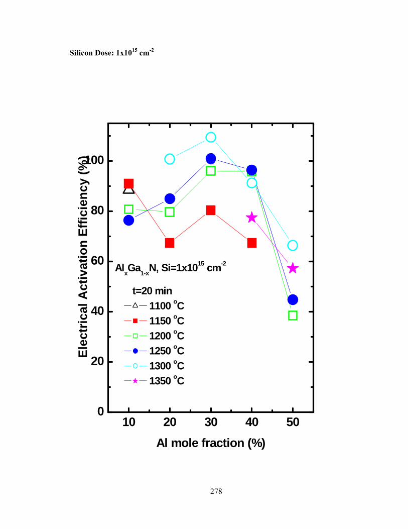
Silicon Dose: 1x1015 cm-2
10 20 30 40 500
20
40
60
80
100
Elec
tric
al A
ctiv
atio
n Ef
ficie
ncy
(%)
Al mole fraction (%)
t=20 min 1100 oC 1150 oC 1200 oC 1250 oC 1300 oC 1350 oC
AlxGa1-xN, Si=1x1015 cm-2
278

10 20 30 40 500
20
40
60
80
100
Mob
ility
(cm
2 /V.s
)
AlxGa1-xN, Si=1x1015 cm-2
t=20 min1100 oC 1150 oC1200 oC 1250 oC1300 oC 1350 oC
Al mole fraction (%)
279

10 20 30 40 500
100
200
300
400
500
600
700R
esis
tivity
(Ω /s
q)
AlxGa1-xN, Si=1x1015 cm-2
t=20 min1100 oC 1150 oC1200 oC 1250 oC1300 oC 1350 oC
Al mole fraction (%)
280

References
1. Houglum, Rodger J. Electronics: Concepts, Applications and History. Boston, Massachusetts: Breton Publishers (1985).
2. Wilson, A. H. Proceedings of the Royal Society A, 133:458 (1931).
3. Bhattacharya, Pallab, Semiconductor Optoelectronic Devices Second Edition.
New Jersey: Prentice Hall (1997).
4. Neaman, Donald A. Semiconductor Physics and Devices Basic Principles. New York: McGraw-Hill (2003).
5. Aschroft, Neil and David Mermin. Solid State Physics. United States of
America: Thompson Learning (1976).
6. Tolbert, Leon M., B. Ozpineci, S. K. Islam and M. S. Chinthavali. “Wide Band Gap Semiconductors for Utility Applications,” Power and Energy Systems, 379: 80 (2003).
7. Materials for High Temperature Semiconductor Devices, the National
Materials Advisory Board, Committee on Engineering and Technical Systems, National Research Council, NMAB-474, Washington D. C: National Academy Press (1995).
8. Nepal, N., L. Nakarmi, J. Y. Lin and H. X. Jiang. “Photoluminescence Studies
of Impurity Transitions in AlGaN Alloys,” Applied Physics Letters, 89: 092107 (2006).
9. Pavlidis, Dimitris. “Recent Advances in III-V Electronics,” Electron Device
Meeting, IEDM Technical Digest, IEEE International: 795-798 (2004).
10. Yu, Haijing, L. McCarthy, S. Rajan, S. Keller, S. Denbaars, J. Speck and U. Mishra. “Ion Implanted AlGaN-GaN HEMTs with Nonalloted Ohmic Contacts,” IEEE Electron Device Letters, 26(5): 283-285 (2005).
11. Hui, Rongqing, Yueting Wan, Jing Li, Sixuan Jin, Jingyu Lin and Hongxing
Jiang. “III-Nitride-Based Planar Lightwave Circuits for Long Wavelength Optical Communications,” IEEE Journal of Quantum Electronics, 41(1): 100-110 (2005).
12. Scofield, James D. Electrical Characterization of Intrinsic and Induced Deep
Level Defects in Hexagonal Si. PhD Dissertation, AFIT/DS/ENP/96-08. Graduate School of Management and Engineering, Air Force Institute of Technology (AU), Wright-Patterson AFB, OH, November 1996.
281

13. Zavada, J. M. and S. J. Pearton. “High Resistivity AlxGa1-xN Layers Grown by
MOCVD,” MIJ-NSR 1(36): (1997).
vice Letters, 10(10): 455-457
ctrochemical Society, 153(8): G734-G737
17. Lin, and H. X. Jiang. “Nitride Deep-
18. . Kim, J. Li, J. Y Lin and H. X. Jiang. “Polarization
sics
19.
lGaN-GaN HEMTs with Nonalloted Ohmic
20.
itsuhiro Tanaka and Osamu Oda. “MOVPE Growth and
er 2001.
14. Baliga, B. J. “Power Semiconductor device Figure of Merit for High Frequency Applications” IEEE Electron De(1989).
15. Nakarmi, M.L., N. Napal, J. Y Lin and H. X. Jiang. “Unitentionally doped n-
type AlxGa1-xN Epilayers,” Applied Physics Letters, 86: 261902 (2005).
16. Kim, Jong Kyu, E. Fred Schubert, Jeahee Cho, Cheolsoo, J. Y. Lin, H. X. Jiang and J. M. Zavada. “GaN Light Emitting Triodes for High-Efficiency Hole Injection,” Journal of the Ele(2006).
Khizar, M., Z. Y. Fan, K. H. Kim, J. Y.ultaviolet Light-emitting Diodes with Microlens Array,” Applied Physics Letters, 86: 172504 (2005).
Shakya, J., K. Knabe, K.Hof III-nitride Blue and Ultraviolet Light Emitting Diodes,” Applied PhyLetters, 86: 091107 (2005).
Yu, Haijing, L. McCarthy, S. Rajan, S. Keller, S. Denbaars, J. Speck and U. Mishra. “Ion Implanted AContacts,” IEEE Electron Device Letters, 26(5): 283-285 (2005).
Miyoshi, Makoto, Masahiro Sakai, Hiroyasu Ishikawa, Takashi Egawa, Takashi Jimbo, MCharacterization of High Al Content AlGaN/GaN Heterostructures on 100 mm Diameter Sapphire Substrates,” Journal of Crystal Growth, 272: 293-299(2004).
21. Lee, Jaesun, Dongmin Liu, Hyeongnam Kim and Wu Lu. “Post Annealing
Efects on Device Performance of AlGaN/GaN HFETs,” Solid-State Electronics, 48: 1855-1859 (2004).
22. Fellows, James. Electrical Activation studies of ion implanted GaN, PhD
Dissertation, AFIT/DS/ENP/02-2. Graduate School of Management and Engineering, Air Force Institute of Technology (AU), Wright-Patterson AFB, OH, Novemb
23. van der Pauw, van der Pauw, L.J. (1958). "A method of measuring specific
resistivity and Hall effect of discs of arbitrary shape, " Philips Research Reports 13: 1–9.
282

24. Yacobi, B. G. Cathodoluminescence Microscopy of Inorganic Solids. New
York: Plenum Press (1990).
25. Fareed, Qhalid, R. Gaska, J. Mickevicius, G. Tamulatis, M. S. Shur, aA. Khan. “Migration Enhanced Metalorganic Chemical Vapor Deposition Aln/GaN
nd M. of
/InN Based Heterostructures,” Compound Semiconductor, 21799: (2005).
26.Aderhold and J. Graul. “The Influence of V/III Ratio in the Initial Growth
27. . Ager III, K. M. Yu, W. Walukiewicz, E. E. Haller, M.C.
Martin, W. R. McKinney, and W. Yang. “Dependence of the Fundamental
28. Ziegler, J. F., J. P. Biersack and U. Littmark. The Stopping and Range of Ions
29. Kachi, S. J. Pearton, F. Ren. “Implantation
temperature dependence of Si activation in AlxGa1-xN,” Applied Physics
30. planted
AlGaN,” Applied Physics Letters, 80: 5 (2002).
31.
32. C, J. Han, S. Van Deusen, R. Buefeld, J. Jun, T. Suski, J. Baranowski,
S. Pearton, and M. Crawford. “Recent Progress in implanting and annealing of
33. Nakarmi, M., N. Nepal, J.Y. Lin, H.X. Jiang. “Unintentionally doped n-type
34.
plnated Si in AlxGa1-xN,” Applied Physics Letters, 86: 192102 (2005).
35. , T.
l and Optical Characterization Studies of Lower Dose Si-
F. Fedler, R. J. Hauenstein, H. Klausing, D. Mistele, O. Semchinova, J.
Stage on the Properties of GaN Epilayer deposited on low temperature AlNBuffer Layer,” Journal of Crystal Growth, 303( 2): 414-418 (2007).
Shan, W, J. W
Band Gap of AlxGa1-xN on Alloy Composition and Pressure,” Journal of Applied Physics, 85(12): 8505-8507 (1999).
in Solids, New York: Pergamon Press (1985).
Irokawa, Y., O. Ishiguro, T.
Letters, 88: 182106 (2006).
Kuckeyev, S. O. and J. S. Williams. “Structural disorder in ion-im
Kuckeyev, S. O., J. Williams, and C. Jagadish. “Ion Beam Defect Processes in group-III nitrides and ZnO,” Vacuum 73: 93-104 (2004).
Zopler, .
GaN and AlxGa1-xN,” Materials Research Society Symposium Proceedings 482: 979-980 (1998).
Al0.67Ga0.33N Epiolayers,” Applied Physics Letters 86: 261902 (2005).
Irokawa, Y., O. Ishiguro, T. Kachi, S. J. Pearton, F. Ren. “Activation characteristics of ion-im +
Ryu, Mee-Yi, Y.K. Yeo, M. Marciniak, T. Zens, E. Moore, R. HengeholdStiener. “Electrica
283

Implanted AlxGa1-xN,” Journal of Electromagnetic Materials, 35(4): 647-653
36. Polyakov, A.Y, N. Smirnov, A. Govorkov, M. Milividskii, J. Redwing, M.
7. Look, D.C. and R. J. Molnar. “Degenerate layer at GaN/sapphire Interface on
38.
ics Letters 85(20): 4669-4671 (2004).
39. i
40. Zavada, J. M. and S. J. Pearton. “High Resistivity Al Ga N Layers Grown by
41. Glaser, E. R. “Optically Detected Magnetic Resonance in GaN Films Grown
1:
42. Ogino, T. and Masaharu Aoki. “Mechanism of Yellow Luminescence in
43. Polyakov, A. Y, M. Shin, J. A. Freitas, M. Showronski, D. W. Grere, R. J.
(1996).
45. Ryu, Mee-Yi, Y.K. Yeo, M. Marciniak, T. Zens, E. Moore, R. Hengehold, T.
-653 (2006).
46.
ealing studies of Si-Implanted Al0.25Ga0.75N,” Physics Stat Sol(c) 1-4, (2003).
(2006).
Shin, M. Skowronski, D. Greve, and R. Wilson. “Properties of Si Donors andPersistent Photoconductivity in AlxGa1-xN,” Solid State Electronics 42(4): 627-635 (1998).
3Hall Effect Measurements,” Applied Physics Letters 70: 3377, (1997).
Zhu, K., M. L. Nakarmi, K. Kim, J.Y. Lin, and H. X Jiang. “Silicon Doping Dependence of Highly Conductive n-type Al0.7Ga0.3N,” Applied Phys
Lee, Cheul-Ro, “N-type Doping Behavior of Al0.15Ga0.85N:Si with Various SIncorporations,” Journal of Crystal Growth 246: 25-30 (2002).
x 1-xMOCVD,” MIJ-NSR 1, 36: (1997).
by OMVPE,” Physical Review B: Condensed Matter Material Physics 513326 (1995).
GaN,” Japanese Journal of Applied Physics 119: 2395-2405 (1980).
Wilson. “On the Origin of Electrically Active Defects in AlxGa1-xN Alloys Grown by OMVPE,” Journal of Applied Physics 80: 6349
44. Nam, K.B., M. L. Nakarmi, J.Y. Lin, and H. X. Jiang. “Deep Impurity
Transitions Involvonig Cation Vacancies and Complexes in AlxGa1-xN alloys,” Applied Physics Letters 86: 222108 (2005).
Stiener. “Electrical and Optical Characterization Studies of Lower Dose Si-Implanted AlxGa1-xN,” Journal of Electromagnetic Materials, 35(4): 647
Ryu, Mee-Yi, E. Chitwood, E. Claunch, Y. Yeo, R. Hengehold, J. Fellows, and T. Steiner. “Ann
284

47.d GaN. MS thesis, AFIT/GAP/ENP/03-01. Graduate School of
Management and Engineering, Air Force Institute of Technology (AU),
48.
. Jimbo. “n-Type Doping Characteristics of O-Implanted AlGaN,” Journal of the Electrochemical Society, 151(12): G801-G804
49. McFall, J. L., R. Hengehold, Y.K. Yeo, J. Van Nostrand and A. Saxler.
:
al of Crystal Growth 279(1-2): 31-36 (2005).
51. stman, S. Bradley, L, Brillson, D. Look,
J. Ku, W. Walukiewicz, M. Furis, and A. Cartwright. “Si Doping of High-Al-
52. Zhu, K., M. Nakarmi, K. Kim, J. Lin and H. Jiang. “Silicon Doping
54. Madelung, Otfried. Semiconductors: Data Handbook 3 Edition, New York:
55. ics and Material
Properties, New York: Springer Publishing, 2001.
56.
12 (2002).
. 1-
rowth 189/190: 528-531 (1998).
Chitwood, Elizabeth. Electrical Activation Studies of AlxGa1-xN and Co-implante
Wright-Patterson AFB, OH, March 2003.
Nakano, Yoshitaka, Osamu Fujishima, T. Kachi, K. Abe, O. Eryu, K. Nakashima, and T
(2005).
“Optical Investigation of MBE Grown Si-doped AlxGa1-xN as a Function of Nominal Al Mole fraction up to 0.5,” Journal of Crystal Growth, 227-228458-465 (2001).
50. Touzi, C., F. Omnes, B. El Jani, P. Gibart. “LP MOVPE Gowth and
Characterization of High Al Content AlxGa1-xN Epilayers,” Journ
Hwang, Jeonghyun, W. Schaff, L. Ea
mole Fraction AlxGa1-xN Alloys with rf Plasma-induced Molecular Beam Epitaxy,” Applied Physics Letters 81(27): 5192-5194 (2002).
Dependence of Highly Conductive n-type Al0.7Ga0.3N,” Applied Physics Letters 85(20): 4669-4671 (2004).
53. Gil, Bernard. Low-Dimensional Nitride Semiconductors. New York: Oxford
University Press (2002).
rd
Springer Publishing, 2003.
Yu, Peter Y. Fundamentals of Semiconductors: Phys
Li, J. N. Oder, M. Nakarmi, J.Lin, and H. Jiang. “Optical and Electrical properties of Mg-Doped p-type AlxGa1-xN,” Applied Physics Letters 80(7): 1210-12
57. Katsuragawa, Maki, S. Sota, M. Komori, C. Anbe, T. Takeuchi, H. Sakai, H
Amano, and I. Akasaki. “Thermal Ionization Energy of Si and Mg in AlxGaxN,” Journal of Crystal G
285

58. Kuckeyev, S.O., J. Williams, J. Zou, C. Jagadish, G. Li. “The effects of imass, energy, dose, flux and irradiation temperature on implantation disoin GaN,” Nuclear Instruments and Methods in Physics Research B 178: 2213 (2001).
on rder 09-
60. Nepal, N., J. Li, M. L. Nakarmi, J. Y. Lin and H. X. Jiang. “Exciton
61. . L. Nakarmi, J. Y. Lin and H. X. Jiang. “Temperature and
Compositional Dependence of the Energy Band Gap of AlxGa1-xN Alloys,”
62. . Schaff. “Time Resolved
Photoluminescence of Si-doped High AL Mole Fraction AlxGa1-xN Epilayers
63. eber. “Donor
and Acceptor Concentrations in Degenerate InN,” Applied Physics Letters
64. g, and R. Wang. “Electrical
Characterization and Surface Morphology of Optimized Ti/Al/Ti/Au Ohmic
(2006).
N Schottky Barrier Height on Al Mole Fraction,” Journal of Applied Physics 87(2): 801-804 (2000).
66. o, C. J. Tun, S. J. Chang,
and G. C. Chi. “ GaN p-n Junction Diode Formed by Si Ion Implantation into
67. n, L. McCarthy, L. P. Smorchkova, P. Chavarkar, T.
Mates, S. Keller, S. DenBaars, J. Speck and Umesh K. Mishra. “Progress in
59. Nam, K.B., M. L. Nakarmi, J.Y. Lin, and H. X. Jiang. “Unique Optical
Properties of AlxGa1-xN Alloys and Related Ultraviolet Emmitters,” AppliedPhysics Letters 84: 5264-5266 (2004).
Localization in AlxGa1-xN Alloys,” Applied Physics Letters 88: 062103 (2006).
Nepal, N., J. Li, M
Applied Physics Letters 87: 242104 (2005).
Furis, M., A. Cartwright, J. Hwang and W
Grown by Plasma-Enhanced Molecular Beam Epitaxy,” Material Research Society Symposium Proceedings 798: Y5.45.1-5 (2004).
Look, D. C., H. Lu, W. J. Schaff, J. Jasinski and Z. Liliental-W
80(2): 258-260 (2002).
Bardwell, J. A., S. Haffouz, H. Tan
Contacts for AlxGa1-xN/GaN HEMTs,” Journal of The Electrochemical Society 153(8): G746-749
65. Qiao, D., L. S. Yu, S. S. Lau, J. M. Redwing, J. Y. Lin and H. X. Jiang. “
Dependance of Ni/ AlxGa1-x
Lee, M. L., J. K. Sheu, L. S. Yeh, M.S. Tsai, C. J. Ka
p-GaN,” Solid-State Electronics 46: 2179-2183 (2002).
Xing, H., D. S. Gree
Gallium Nitride-based Bipolar Transistors,” Bipolar/BiCMOS Circuits and Technology Meeting, Proceedings of the 2001:125-130 (2001).
286

68. Fellows, James A., Y. K. Yeo, Mee-Yi Ryu, and R. L. Hengehold. “Electricaand Optical Activation Studies of Si-Implanted GaN,” Journal of Electronic Materials 34(8): 1157-1164 (2005).
l
69. Seghier, D., H. P. Gislason. “Effect of Hydrogenation on the Electrical
70. Piazza, Gianluca, P. J. Stephanou and A. P. Pisano. “AlN Contour-Mode
,” Solid -64
72. Look, David C., Electrical Characterization of GaAs Materials and Devices.
73.
B 21 (6): 2558-2563 (2003).
en deficiency
76. Lee, Sung-Nam, JoongKon Son, Tan Sakong, Wonseok Lee, Hosun Peaek,
CVD,” Journal of Crystal Growth 272: 455-459 (2004).
77.
1994).
79. Ziegler, James F. Ion Implantation – Science and Technology 2004 Edition.
New York: IIT Press, 2004.
Properties of n-type AlxGa1-xN,” Journal of Physics D: Applied Physics 37: 10-12 (2004).
Vibrating RF MEMS for Next Generation Wireless CommunicationsState Device Research Conference, Proceedings of the 36th European: 61(2006).
71. Sze, S. M. Physics of Semiconductor Devices (2nd Edition). New York: John
Wiley & Sons, 1981.
New York: John Wiley & Sons, 1989.
Shklovskii, B. I., and A. L. Efros, Electrical Properties of Doped Semiconductors. Berlin: Springer-Verlag, 1984.
74. Bradley, S.T., S. H. Goss, L. J. Brillson, J. Hwang, W. J. Schaff. “Deep level
defects and doping of high Al mole fraction AlxGa1-xN,” Journal of VacuumScience and Technology
75. Hashizume, Tamotsu, and Hideki Hasegawa. “Effects of nitrog
on the electronic properties of AlxGa1-xN surfaces subject to thermal and plasma radiation,” Applied Surface Science 234 (1-4): 387-394 (2004).
Euijoon Yoon, Jiyoung Kim, Yong-Hoon Cho, Okhyun Nam, and Yongjo Park. “Investigation of optical and electrical properties of Mg-doped p-InxGa1-xN, p-GaN and p-AlxGa1-xN grown by MO
Christensen, N.E., and Gorczyca I. “Optical and structural properties of III-V nitrides under pressure,” Physics Review B: 4397-4415 (
78. Neilson, Karl Ove. “Accelerators with ion sources for heavy radioactive
decay,” Presented at the Conference for Applications of Ion Beams to Semiconductors Technology, Grenoble. May 1967. www.phys.au.dk/main/historie/giraf/home.htm
287

288
80. Pearton, S. J. “ GaN: Processing, defects and devices,” Journal of Applied Physics 86(1): 1-78 (1999).

REPORT DOCUMENTATION PAGE Form Approved
OMB No. 074-0188
The public reporting sting data sources, gathering and maintaining the da e collection of information, including suggestions for re gton Headquarters Services, Directorate for Information Operations and Reports (0704-0188), 1215 Jefferson Davis Highway, Suite 1 4, Ar are that notwithstanding any other provision of law, no person shall be subject to an penalty for failing to comply with a collection of inform on if it does not display a currently valid OMB control number.
PLEASE DO NO RETURN YOUR FORM TO THE ABOVE ADDRESS.
burden for this collection of information is estimated to average 1 hour per response, including the time for reviewing instructions, searching exita needed, and completing and reviewing the collection of information. Send comments regarding this burden estimate or any other aspect of th
ducing this burden to Department of Defense, Washinlington, VA 22202-4302. Respondents should be aw20
atiT
1. REPORT DATE (DD-MM-YYYY) 12-2007
2. REPORT TYPE Doctoral Dissertation
3. DATES COVERED (From – To) Oct 2004 – Dec 2007
5a. CONTRACT NUMBER
5b. GRANT NUMBER
4. TITLE AND SUBTITLE
ELECTRICAL ACTIVATION STUDIES OF SILICON IMPLANTED ALUMINUM GALLIUM NITRIDE WITH HIGH ALUMINUM MOLE FRACTION 5c. PROGRAM ELEMENT NUMBER
5d. PROJECT NUMBER
5e. TASK NUMBER
6. AUTHOR(S) Elizabeth A. Moore
5f. WORK UNIT NUMBER
7. PERFORMING ORGANIZATION NAME(S) AND ADDRESS(ES) Air Force Institute of Technology Graduate School of Engineering and Management (AFIT/EN) 2950 P Street, Building 640 WPAFB OH 45433-7765
8. PERFORMING ORGANIZATION REPORT NUMBER
AFIT/DS/ENP/08-D01
10. SPONSOR/MONITOR’S ACRONYM(S)
AFOSR/NE
9. SPONSORING/MONITORING AGENCY NAME(S) AND ADDRESS(ES) Air Force Office of Scientific Research Dr. Don Silversmith 4015 Wilson Blvd. Arlington, VA 22203
11. SPONSOR/MONITOR’S REPORT
NUMBER(S)
12. DISTRIBUTION/AVAILABILITY STATEMENT
APPROVED FOR PUBLIC RELEASE; DISTRIBUTION UNLIMITED.
13. SUPPLEMENTARY NOTES
14. ABSTRACT This research demonstrates a method for producing highly conductive Si-implanted n-type aluminum gallium nitride
(AlxGa1-xN) alloys, and represents a comprehensive analysis of the resulting material's electrical and optical properties as a function of Al mole fraction, anneal temperature, anneal time, and implantation dose. Highly conductive alloys are critical to the fabrication of devices operating in deep UV, high-temperature, high-power, and high-frequency environments, and thus this research is significant in regard to the application of such devices. The AlxGa1-xN wafers of this study, with Al concentrations of 10 to 50%, were implanted at room temperature with silicon ions at energies of 200 keV with doses of 1x10¹⁴, 5x10¹⁴, and 1x1015 cm-2 and annealed from 1100 to 1350 ºC for 20 to 40 minutes in flowing nitrogen. Excellent activation was achieved for each of the implanted silicon doses for all of the five Al mole fractions studied, with most activation efficiencies above 90%. These activation efficiencies are the highest reported activations, to the best of my knowledge. The mobilities were found to decrease as the Al concentration of the AlxGa1-xN was increased from 10 to 50% and also as the implanted silicon dose was increased. Typical mobilities ranged from 101 cm2/V·s for the Al0.1Ga0.9N implanted with 1x1014 cm-2 silicon ions to 35 cm2/V·s obtained for the Al0.5Ga0.5N implanted with 1x1015 cm-2 silicon ions. The cathodoluminescence results support the electrical results in determining the optimal annealing conditions. 15. SUBJECT TERMS
Electrical activation efficiency, AlGaN, Hall effect, Ion Implantation, Cathodoluminescence 16. SECURITY CLASSIFICATION OF: 19a. NAME OF RESPONSIBLE PERSON
Dr. Yung Kee Yeo, ENP a. REPORT U
b. ABSTRACT U
c. THIS PAGE U
17. LIMITATION OF
ABSTRACT UU
18. NUMBER OF
PAGES 312 19b. TELEPHONE NUMBER (Include area code)
(937) 255-3636, ext 5432
Standard Form 298 (Rev. 8-98) Prescribed by ANSI Std.
Z39-18

290