Physical, electrical, and optical properties of SF-PECVD-grown hydrogenated microcrystalline silicon...
11
Abstract Characterization results on hydrogenated microcrystalline silicon (lc-Si:H) thin films grown in a Saddle Field (SF) PECVD system are presented. The microcrystalline content of the films is controlled by the application of a positive electrical bias to the film growth surface. The results of photoluminescence, atomic force microscopy, infrared-absorption, and electrical conductivity studies are presented. The results correlate to the changing microcrystalline content of the films in the same way as when micro- crystalline content is influenced through growth parameters such as hydrogen dilution in other CVD techniques. 1 Introduction The microcrystalline content of Saddle Field (SF)- PECVD-grown lc-Si:H shows dependence on many growth parameters (pressure, hydrogen dilution, flow- rate, plasma power density), much as samples grown in other CVD systems [1]. Previous work on the growth of lc-Si:H in the SF-PECVD system has also shown that the electrical potential at the substrate surface is crucial to the formation of the microcrystalline phase. The substrate surface must either have a positive voltage applied to it [2] or be electrically floating [3] to encourage the growth of microcrystalline material. The technique of applying a voltage to the growth surface only yields microcrystalline material under specific pressure and voltage conditions (E. Johnson et al., submitted). It has been proposed that this effect is due to the reduced ion bombardment of the growth surface. The importance of ion-bombardment during lc-Si:H growth has been studied in other growth technologies [4], and elevated ion bombardment generally reduces the microcrystalline content of the bulk and can even result in a layered structure in the resulting films [5]. Energetic ions amorphize the top-most layer and the transformation to microcrystalline material occurs in a subsurface region. In this way, ion bombardment affects not just the microscopic properties of the material, but will affect devices through the creation of undesired interfaces. Addressing this effect is crucial if the SF-PECVD technique is to be applied to large area electronic growth, and this work explores the effect on material properties that result in attempting to mini- mize ion bombardment through the use of an applied electrical bias. In this work, the optical and electrical character- ization of matched sets of lc-Si:H films grown on test- appropriate substrates is presented. The films are grown in a SF-PECVD system using growth conditions near the threshold of microcrystalline growth and the surface potential is actively controlled with an external voltage source. We present here the results of tem- perature-dependent photoluminescence (PL), atomic force microscopy (AFM), Fourier transform infrared absorption (FTIR), and four-point temperature- dependent conductivity. We correlate this data to E. V. Johnson S. Hoogland E. Klem N. Kherani S. Zukotynski (&) Department of Electrical and Computer Engineering University of Toronto, Toronto, Ontario, CanadaM5S 3G4 e-mail: [email protected] Present address: E. V. Johnson LPICM, E ´ cole Polytechnique, Palaiseau Cedex 91128, France J Mater Sci: Mater Electron (2006) 17:789–799 DOI 10.1007/s10854-006-0025-0 123 Physical, electrical, and optical properties of SF-PECVD-grown hydrogenated microcrystalline silicon with growth surface electrical bias Erik V. Johnson Sjoerd Hoogland Ethan Klem Nazir Kherani Stefan Zukotynski Received: 9 January 2006 / Accepted: 11 March 2006 Ó Springer Science+Business Media, LLC 2006
Transcript of Physical, electrical, and optical properties of SF-PECVD-grown hydrogenated microcrystalline silicon...
Abstract Characterization results on hydrogenated
microcrystalline silicon (lc-Si:H) thin films grown in a
Saddle Field (SF) PECVD system are presented. The
microcrystalline content of the films is controlled by
the application of a positive electrical bias to the film
growth surface. The results of photoluminescence,
atomic force microscopy, infrared-absorption, and
electrical conductivity studies are presented. The
results correlate to the changing microcrystalline
content of the films in the same way as when micro-
crystalline content is influenced through growth
parameters such as hydrogen dilution in other CVD
techniques.
1 Introduction
The microcrystalline content of Saddle Field (SF)-
PECVD-grown lc-Si:H shows dependence on many
growth parameters (pressure, hydrogen dilution, flow-
rate, plasma power density), much as samples grown in
other CVD systems [1]. Previous work on the growth
of lc-Si:H in the SF-PECVD system has also shown
that the electrical potential at the substrate surface is
crucial to the formation of the microcrystalline phase.
The substrate surface must either have a positive
voltage applied to it [2] or be electrically floating [3] to
encourage the growth of microcrystalline material. The
technique of applying a voltage to the growth surface
only yields microcrystalline material under specific
pressure and voltage conditions (E. Johnson et al.,
submitted). It has been proposed that this effect is due
to the reduced ion bombardment of the growth surface.
The importance of ion-bombardment during lc-Si:H
growth has been studied in other growth technologies
[4], and elevated ion bombardment generally reduces
the microcrystalline content of the bulk and can even
result in a layered structure in the resulting films [5].
Energetic ions amorphize the top-most layer and the
transformation to microcrystalline material occurs in a
subsurface region. In this way, ion bombardment
affects not just the microscopic properties of the
material, but will affect devices through the creation of
undesired interfaces. Addressing this effect is crucial if
the SF-PECVD technique is to be applied to large area
electronic growth, and this work explores the effect on
material properties that result in attempting to mini-
mize ion bombardment through the use of an applied
electrical bias.
In this work, the optical and electrical character-
ization of matched sets of lc-Si:H films grown on test-
appropriate substrates is presented. The films are
grown in a SF-PECVD system using growth conditions
near the threshold of microcrystalline growth and the
surface potential is actively controlled with an external
voltage source. We present here the results of tem-
perature-dependent photoluminescence (PL), atomic
force microscopy (AFM), Fourier transform infrared
absorption (FTIR), and four-point temperature-
dependent conductivity. We correlate this data to
E. V. Johnson Æ S. Hoogland Æ E. Klem Æ N. Kherani ÆS. Zukotynski (&)Department of Electrical and Computer EngineeringUniversity of Toronto, Toronto, Ontario, CanadaM5S 3G4e-mail: [email protected]
Present address:E. V. JohnsonLPICM, Ecole Polytechnique, Palaiseau Cedex 91128,France
J Mater Sci: Mater Electron (2006) 17:789–799
DOI 10.1007/s10854-006-0025-0
123
Physical, electrical, and optical properties of SF-PECVD-grownhydrogenated microcrystalline silicon with growth surfaceelectrical bias
Erik V. Johnson Æ Sjoerd Hoogland ÆEthan Klem Æ Nazir Kherani Æ Stefan Zukotynski
Received: 9 January 2006 / Accepted: 11 March 2006� Springer Science+Business Media, LLC 2006

previously measured microcrystalline content (as
determined by Raman scattering). We show that the
use of substrate bias during the growth of microcrys-
talline material in a SF-PECVD system impacts all its
physical, optical, and electrical properties to a signifi-
cant extent, and that this impact can be correlated with
the microcrystalline phase transition.
2 Experimental procedure
All of the samples for this study were grown in a
SF-PECVD system, which employs a semi-transparent
central anode to extend the mean free path of electrons
and increase their likelihood of ionizing and dissoci-
ating collisions. Twenty sets of samples were grown for
this study. All of the samples were grown under similar
conditions, tabulated in Table 1.
Further detail about the growth conditions and the
topology for the application of a substrate surface bias
can be found in previous publications [2]. For these sets
of samples, only the chamber pressure and the sub-
strate surface electrical potential (Vsub) were actively
varied. The chamber pressure was varied from 100 to
300 mTorr and Vsub from 150 V to 250 V.
The PL spectra of the lc-Si:H samples deposited by
SF-PECVD on f-SiO2 were taken using a tunable
Spectra Physics Mai Tai diode-pumped Ti:Sapphire
laser operating at 800 nm, and frequency doubled with
a KTP crystal to 400 nm. The sample was cooled
through contact with a liquid He cooled cold-finger,
and the temperature was measured with thermocou-
ples both at the cold-finger and on the sample surface.
The temperature difference between the two was sig-
nificant, so the cold finger temperature is considered a
lower limit on the sample temperature and the surface
temperature an upper limit.
The surface morphology of the films deposited on
f-SiO2 were analyzed through AFM using a Digital
Instruments Nanoscope in tapping mode. The sampled
area of the film was 750 nm · 750 nm.
The films to be analyzed through FTIR were
deposited on c-Si wafers for sufficient transparency in
the infrared. The error introduced by coherent reflec-
tion in the film is ignored [6], so the absolute values of
the atomic density may be overestimated as the films
are very thin. However, the relative density is the more
important parameter in this study.
The films grown on f-SiO2 were deposited in the
Van Der Pauw configuration and were analyzed
through temperature dependent four-point conductiv-
ity. These measurements were taken over a tempera-
ture range from 390 K to 430 K—well below the
sample growth temperature but in the temperature
range for extended state conduction—and were done
in high vacuum at an estimated pressure of 10)6 Torr.
3 Results and discussion
3.1 Temperature-dependent PL
The different PL signatures of a-Si:H and lc-Si:H
clearly define the two materials. In a-Si:H, PL shows a
broad dominant peak at 1.3–1.5 eV which is attributed
to tail state recombination [7], and another much
weaker peak at 0.9–1.0 eV which may be attributed to
defect states at mid-gap [8]. In lc-Si:H, a narrow
0.9 eV peak dominates, particularly at low-tempera-
tures [9], and there is a second, much broader peak at
~1.2 eV. The low energy peak is attributed to a
recombination center, due to its narrow linewidth,
which indicates a crystalline or ordered character to
the system. Authors have alternatively declared this
peak a result of dangling bond luminescence in the
a-Si:H matrix, or to a transition between bandtail states
in the lc-Si:H gap [10]. Savchouk et al. [10] used poly-
Si deposited on glass by pyrolysis at 625�C. Post-
deposition hydrogenation increased the intensity of
the PL by a factor of 3–4, indicating the suppression of
a non-radiative recombination channel, most likely
defects at grain boundaries. Komuro et al. [11] have
demarcated three distinct peaks in the PL spectrum
of lc-Si:H: one below 0.8 eV, one between 0.9 eV
and 1.0 eV, and the tail-to-tail amorphous peak at
1.2–1.4 eV. They observed a much shorter lifetime for
the lower energy peaks, and maintain that the 0.8 eV
peak is due solely to the a-Si:H defects. Merdzhanova
et al. [12] have simultaneously observed both the
0.8 eV and the 0.9–1.0 eV peaks but attributed the
peak separation to interference effects.
The transition from one material phase to the other
over a series of depositions due to changing conditions
can be followed by observing the changing PL peaks,
as explored by Yue et al. [13] with samples grown by
HW-CVD with varying degrees of hydrogen dilution.
They have attributed certain luminescence peaks to
different types of boundaries—a boundary between
c-Si islands and the a-Si:H matrix at ~1.0 eV, and the
Table 1 Growth conditionsFlow rate (FR) = 5 sccmDilution ratio (R),SiH4:H2 = 1:10Substrate temperature(Tsub) � 180�CAnode current(IAN) = 20 mA
790 J Mater Sci: Mater Electron (2006) 17:789–799
123
other between c-Si grains at 0.9 eV. A closer exami-
nation of their data shows three peaks, as identified in
[11] and [14], where the peak at 0.9 eV is dominant at
high microcrystalline fractions and shifts towards
1.0 eV with increasing amorphous content. A second
peak emerges near 1.25 eV with decreasing micro-
crystalline content, and a third peak near 1.4 eV in
amorphous samples.
So in summary, a total of four distinct peaks can be
identified at the following locations:
(1) £0.8 eV attributed to dangling bond recombina-
tion in a-Si:H.
(2) 0.9–1.0 eV, attributed to either the electronic tail
recombination in lc-Si:H grains or recombination
at grain boundaries (0.9 eV for GB’s between
crystallites and 1.0 eV for GB’s between crystal-
lites and amorphous matrix).
(3) 1.2–1.3 eV, attributed to a shifted a-Si:H tail-
to-tail transition peak but only present when
some microcrystalline fraction occurs.
(4) 1.3–1.4 eV, attributed to tail-to-tail recombina-
tion in a-Si:H.
Han et al. [14] performed both front and back side
illumination of the films for PL and observed signifi-
cantly different PL in each case. In the same sample,
the 1.2–1.3 eV peak is dominant for film side illumi-
nation, while the ~1.4 eV peak is dominant for back-
side illumination. This suggests that the 1.2–1.3 eV
peak is indicative of either protocrystalline material, or
very small crystallites.
The coincidence of the PL peaks in a-Si:H
and lc-Si:H make data interpretation difficult, but the
emergence of the peak at 0.9–1.0 eV in lc-Si:H at
low-temperatures is a good diagnostic measure of the
predominance of lc-Si:H in the material. This peak
shows a strong temperature dependence, whereas the
a-Si:H peak is much more temperature stable [9].
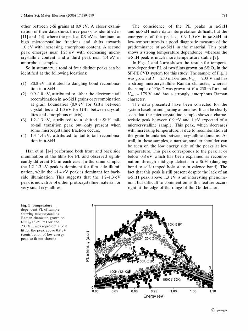
In Figs. 1 and 2 are shown the results for tempera-
ture-dependent PL of two films grown on f-SiO2 in the
SF-PECVD system for this study. The sample of Fig. 1
was grown at P = 250 mTorr and Vsub = 200 V and has
a strong microcrystalline Raman character, whereas
the sample of Fig. 2 was grown at P = 250 mTorr and
Vsub = 175 V and has a strongly amorphous Raman
character.
The data presented have been corrected for the
system baseline and grating anomalies. It can be clearly
seen that the microcrystalline sample shows a charac-
teristic peak between 0.9 eV and 1 eV expected of a
microcrystalline sample. This peak, which decreases
with increasing temperature, is due to recombination at
the grain boundaries between crystalline domains. As
well, in these samples, a narrow, smaller shoulder can
be seen on the low energy side of the peaks at low
temperature. This peak corresponds to the peak at or
below 0.8 eV which has been explained as recombi-
nation through mid-gap defects in a-Si:H (dangling
bond to self-trapped hole state in valence band). The
fact that this peak is still present despite the lack of an
a-Si:H peak above 1.3 eV is an interesting phenome-
non, but difficult to comment on as this feature occurs
right at the edge of the range of the Ge detector.
Fig. 1 Temperaturedependent PL of sampleshowing microcrystallineRaman character, grown onf-SiO2 at 250 mTorr and200 V. Lines represent a bestfit for the peak above 0.9 eV(contribution of low-energypeak to fit not shown)
J Mater Sci: Mater Electron (2006) 17:789–799 791
123
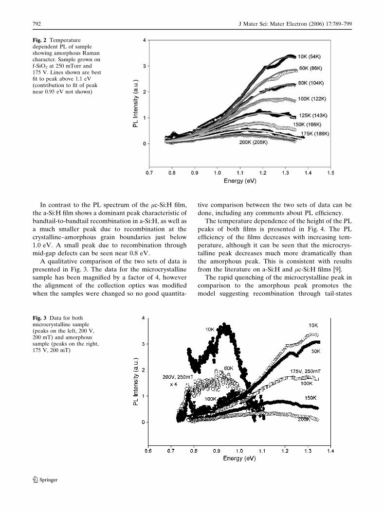
In contrast to the PL spectrum of the lc-Si:H film,
the a-Si:H film shows a dominant peak characteristic of
bandtail-to-bandtail recombination in a-Si:H, as well as
a much smaller peak due to recombination at the
crystalline–amorphous grain boundaries just below
1.0 eV. A small peak due to recombination through
mid-gap defects can be seen near 0.8 eV.
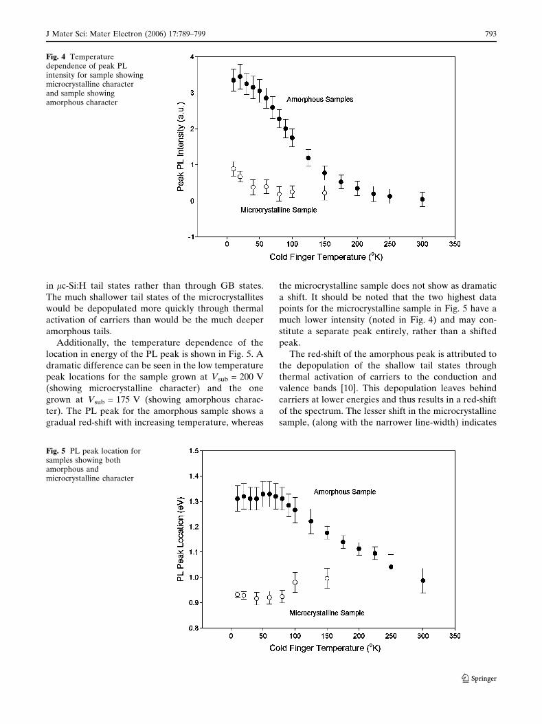
A qualitative comparison of the two sets of data is
presented in Fig. 3. The data for the microcrystalline
sample has been magnified by a factor of 4, however
the alignment of the collection optics was modified
when the samples were changed so no good quantita-
tive comparison between the two sets of data can be
done, including any comments about PL efficiency.
The temperature dependence of the height of the PL
peaks of both films is presented in Fig. 4. The PL
efficiency of the films decreases with increasing tem-
perature, although it can be seen that the microcrys-
talline peak decreases much more dramatically than
the amorphous peak. This is consistent with results
from the literature on a-Si:H and lc-Si:H films [9].
The rapid quenching of the microcrystalline peak in
comparison to the amorphous peak promotes the
model suggesting recombination through tail-states
Fig. 3 Data for bothmicrocrystalline sample(peaks on the left, 200 V,200 mT) and amorphoussample (peaks on the right,175 V, 200 mT)
Fig. 2 Temperaturedependent PL of sampleshowing amorphous Ramancharacter. Sample grown onf-SiO2 at 250 mTorr and175 V. Lines shown are bestfit to peak above 1.1 eV(contribution to fit of peaknear 0.95 eV not shown)
792 J Mater Sci: Mater Electron (2006) 17:789–799
123
in lc-Si:H tail states rather than through GB states.
The much shallower tail states of the microcrystallites
would be depopulated more quickly through thermal
activation of carriers than would be the much deeper
amorphous tails.
Additionally, the temperature dependence of the
location in energy of the PL peak is shown in Fig. 5. A
dramatic difference can be seen in the low temperature
peak locations for the sample grown at Vsub = 200 V
(showing microcrystalline character) and the one
grown at Vsub = 175 V (showing amorphous charac-
ter). The PL peak for the amorphous sample shows a
gradual red-shift with increasing temperature, whereas
the microcrystalline sample does not show as dramatic
a shift. It should be noted that the two highest data
points for the microcrystalline sample in Fig. 5 have a
much lower intensity (noted in Fig. 4) and may con-
stitute a separate peak entirely, rather than a shifted
peak.
The red-shift of the amorphous peak is attributed to
the depopulation of the shallow tail states through
thermal activation of carriers to the conduction and
valence bands [10]. This depopulation leaves behind
carriers at lower energies and thus results in a red-shift
of the spectrum. The lesser shift in the microcrystalline
sample, (along with the narrower line-width) indicates
Fig. 4 Temperaturedependence of peak PLintensity for sample showingmicrocrystalline characterand sample showingamorphous character
Fig. 5 PL peak location forsamples showing bothamorphous andmicrocrystalline character
J Mater Sci: Mater Electron (2006) 17:789–799 793
123

a more ordered population is producing this PL peak,
which supports both the models using tail-state
recombination in the crystallites as well as GB
recombination.
The results of the temperature dependent PL study
on the films demonstrate the powerful effect that
substrate bias plays on the resulting film properties in
the SF-PECVD system. It must be restated that the
two films under study were grown under identical
growth conditions to similar thickness, except for a
difference in ion bombardment energy reduced by an
externally applied substrate bias. These films show PL
properties that encompass those exhibited by films
grown under dramatically different growth conditions
in other systems.
3.2 Atomic force microscopy
AFM is an important diagnostic tool for the growth
of lc-Si:H. It allows characterization of the surface
morphology and this gives information about the
microcrystalline content of the film as explored in the
work of Collins et al., who observed that the transition
to microcrystalline growth is accompanied by a
roughening of the growth surface [15, 16].
AFM characterization was performed on the sam-
ples grown on f-SiO2. In Fig. 6(a)–(f) are presented the
scans for these samples. There is clearly a correlation
between the surface roughness and the microcrystal-
linity in this limited set of samples. The two films that
showed high microcrystalline content (deposition con-
ditions of 250 mTorr/200 V (Fig. 6a) and 200 mTorr/
225 V (Fig. 6d)) also show much more surface rough-
ness. A plot of the roughness layer thickness depen-
dence on the microcrystalline content is presented in
Fig. 7.
Clearly, the microcrystalline content of the films and
the surface roughness are strongly correlated, as
described in the literature for lc-Si:H films grown in
other CVD systems. The microcrystalline content of
the SF-PECVD films has been solely modified through
the application of a substrate surface electrical bias.
3.3 FTIR spectroscopy—hydrogen content and
microcrystallinity in lc-Si:H films
The hydrogen content and the configuration of
hydrogen in lc-Si:H also gives interesting information
about the structure of the material. Kroll et al. [17]
studied the hydrogen concentration of films of varying
microcrystalline fraction (controlled by H2-dilution).
As hydrogen dilution of the supply gas is increased
and the films become protocrystalline, the hydrogen
content first peaks, and then decreases to a few atomic
percent. As well, the configuration of the remaining
hydrogen changes from mostly mono-hydride (Si–H)
configuration to di-hydride (Si–H2). This effect has
also been noted by Fujiwara et al. [18] at interfaces
between lc-Si:H and ZnO, indicating that it is intrinsic
to the phase transition of proto-Si:H into lc-Si:H.
Fig. 6 AFM scans of films grown on f-SiO2 with varyingpressures and substrate bias voltages. (a) 250 mTorr and200 V, (Xl c = 64.4%), (b) 250 mTorr and 175 V, (Xlc= 4.7%),(c) 200 mTorr and 250 V, (Xl c = 44.8%), (d) 200 mTorr and225 V, (Xl c = 63.0%), (e) 200 mTorr and 200 V, (Xlc = 14.5%),and (f) 200 mTorr and 175 V, (Xl c = 21.5%)
794 J Mater Sci: Mater Electron (2006) 17:789–799
123

Silicon–hydrogen bonds contribute to the absorp-
tion spectrum through three modes: stretching (near
2000 cm)1), bending (near 850 cm)1) and wagging
(640 cm)1). Isolated Si–H bonds contribute to the
wagging peak at 640 cm)1, and also to a stretching
peak at 2000 cm)1. The presence of silicon dihydride is
indicated by a bending mode near 880 cm)1, while
silicon trihydride and polyhydrides ðSiH2Þn create a
doublet with peaks at 890 cm)1 and 850 cm)1. All of
the bonded hydrogen, however, contribute to the
wagging mode at ~640 cm)1, so the bonded hydrogen
content NHB can be best determined from this peak as
NHB ¼ CB
ZaðxÞx
dx; ð1Þ
where CB is the oscillator strength, x is the optical
frequency of the light, and a is the optical absorption.
The peak in a(x)/x, can be fit to a Gaussian with
amplitude a0 and standard deviation r0, so the total
hydrogen content will be given as
NHB ¼ CBa0r0
ffiffiffiffiffiffi2pp
: ð2Þ
This relationship can then be used to determine
the atomic percentage of hydrogen, assuming an
atomic density of 5.0 · 1022 cm)3, and a CB value of
2 · 1019 cm)3 [19]. The peaks near 2000–2100 cm)1 are
also often used to obtain hydrogen content. The dif-
ferent oscillator strengths for each of the stretching
modes made this calculation difficult for the samples
deposited for this study as many hydrogen-bonding
configurations were observed in the FTIR spectra.
The important role of hydrogen in initiating micro-
crystalline growth is well documented in the literature.
All the growth models rely on the participation of
hydrogen—either through an etching process, a surface
mobility process, or a subsurface chemical process. In
particular, the chemical annealing model relies on a
threshold hydrogen content in the film so that micro-
crystalline sites can nucleate. In Fig. 8, the atomic
hydrogen content of the films grown in this study
is plotted as a function of microcrystalline content.
Despite a fair amount of uncertainty,1 a pattern
indicative of hydrogen-instigated microcrystalline
growth can be seen. As films go from conditions that
generate amorphous films to conditions that result in
microcrystalline films, the hydrogen content increases,
peaks, and then decreases. The decrease occurs as
crystalline sites begin to expand and the chemical
gradient pushes H out of the crystallites, into grain-
boundaries, voids, and towards the surface of the film.
Some of the low-microcrystallinity films show a dis-
proportionally high hydrogen content. This result may
be due to these films being porous or columnar and
having a low density. This theory is supported by a
noticeable Si–O peak near 1000 cm)1, indicating the
deep oxidation of the film, a symptom of low density.
Fig. 6 continued
1 The crystallinity is calculated for films on either SnO2:F, f-SiO2, or CG7059 substrates, whereas the H-content is calculatedfor films on crystalline wafers.
J Mater Sci: Mater Electron (2006) 17:789–799 795
123
Additional information about the films can be
obtained by observation of the stretching mode peaks
around 2000 cm)1. In this area, isolated Si–H bonds
contribute to a peak at 2000 cm)1, clustered Si–H’s
create a peak at 2080 cm)1, and Si–H2 bonds show up
in a peak at 2120 cm)1. To summarize these bonding
configurations, the microstructure parameter R* is
often used. It is defined as the ratio of the integrated
intensity of the peaks above 2000 cm)1 (the peaks
associated with clustered Si–H and Si–H2) to the
integrated intensity of all the peaks in the 1900–
2200 cm)1 range. It gives a good indication of the
quality of amorphous films; films with microstructure
parameters below 0.1 have carrier mobilities that make
them suitable for use in photovoltaic devices.
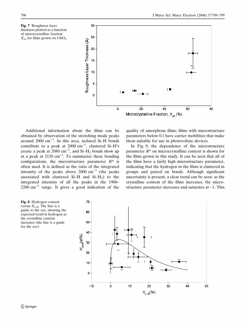
In Fig. 9, the dependence of the microstructure
parameter R* on microcrystalline content is shown for
the films grown in this study. It can be seen that all of
the films have a fairly high microstructure parameter,
indicating that the hydrogen in the films is clustered in
groups and paired on bonds. Although significant
uncertainty is present, a clear trend can be seen: as the
crystalline content of the films increases, the micro-
structure parameter increases and saturates at ~1. This
Fig. 7 Roughness layerthickness plotted as a functionof microcrystalline fractionXlc for films grown on f-SiO2
Fig. 8 Hydrogen contentversus Xc-Si. The line is aguide to the eye, showing theexpected trend in hydrogen asthe crystalline contentincreases (the line is a guidefor the eye)
796 J Mater Sci: Mater Electron (2006) 17:789–799
123
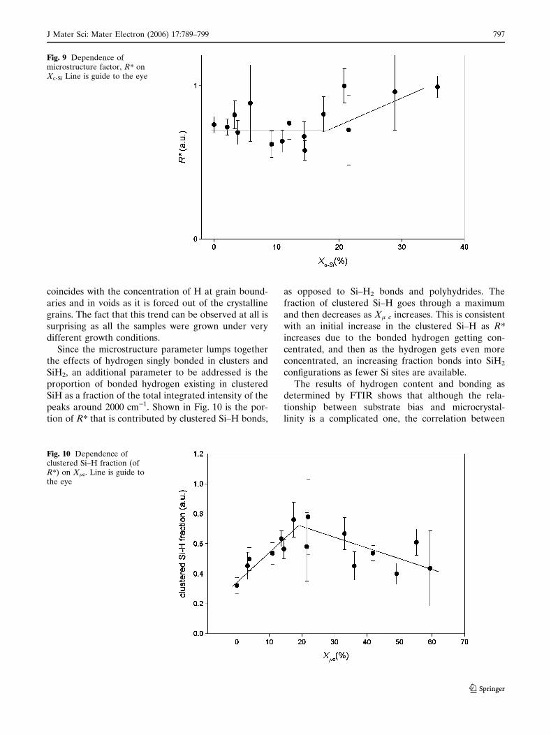
coincides with the concentration of H at grain bound-
aries and in voids as it is forced out of the crystalline
grains. The fact that this trend can be observed at all is
surprising as all the samples were grown under very
different growth conditions.
Since the microstructure parameter lumps together
the effects of hydrogen singly bonded in clusters and
SiH2, an additional parameter to be addressed is the
proportion of bonded hydrogen existing in clustered
SiH as a fraction of the total integrated intensity of the
peaks around 2000 cm)1. Shown in Fig. 10 is the por-
tion of R* that is contributed by clustered Si–H bonds,
as opposed to Si–H2 bonds and polyhydrides. The
fraction of clustered Si–H goes through a maximum
and then decreases as Xl c increases. This is consistent
with an initial increase in the clustered Si–H as R*
increases due to the bonded hydrogen getting con-
centrated, and then as the hydrogen gets even more
concentrated, an increasing fraction bonds into SiH2
configurations as fewer Si sites are available.
The results of hydrogen content and bonding as
determined by FTIR shows that although the rela-
tionship between substrate bias and microcrystal-
linity is a complicated one, the correlation between
Fig. 10 Dependence ofclustered Si–H fraction (ofR*) on Xlc. Line is guide tothe eye
Fig. 9 Dependence ofmicrostructure factor, R* onXc-Si Line is guide to the eye
J Mater Sci: Mater Electron (2006) 17:789–799 797
123

microcrystallinity and hydrogen content/bonding is
similar to that observed in a-Si:H/lc-Si:H films grown
in other PECVD systems.
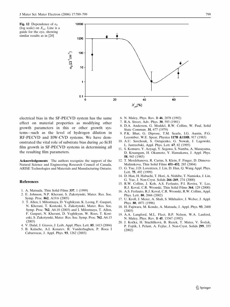
3.4 Temperature dependent conductivity and
microcrystallinity
As in most amorphous films, electronic transport
in lc-Si:H films can happen through a variety of
mechanisms, and the dominant mechanism at any
temperature will dictate the behaviour of electrical
conduction. After Kocka et al. [20], we assume the
primary conduction mechanism for these films to be
carriers excited into the conduction and valence bands,
so the resulting measurements were fit to a tempera-
ture-dependent exponential. From this fit, the activa-
tion energy, EA, and the conductivity prefactor, r0, can
be extracted.
rðTÞ ¼ r0eEA=kT : ð3Þ
In Fig. 11, the variation in EA with Xl c is shown for
films grown on f-SiO2. As the microcrystalline fraction
increases, the activation energy approaches the value
characteristic of lc-Si grains due to an upwards shift in
the Fermi level [20]. This is accompanied by a decrease
of several orders of magnitude in r0, as shown in
Fig. 12. In the literature, this has been attributed to a
change in the conductivity path in lc-Si:H due to the
presence of grain boundaries between large grains,
formed when the films become very microcrystalline. It
has been proposed that the increased barriers at the
grain boundaries make the main lateral conduction
path hopping through tails states below the conduction
band, as opposed to extended state conduction. As the
size of the grains increase, the number of barriers
decreases, although their height does not. This explains
the upward trend in r0 whereas EA shows no such
trend.
The results presented in Figs. 11 and 12 clearly show
that the microcrystalline character of the films domi-
nates the conductivity behaviour. The changes in the
lateral conduction mechanism as the film gains crys-
talline character are clearly seen in the conductivity
prefactor and the activation energy of the conductivity.
Once again, controlling the surface potential of the film
during growth has drastically changed the macroscopic
properties of the resulting film.
4 Conclusions
In this work, we have characterized a set of lc-Si:H
films grown by a novel thin-film deposition technology,
the SF-PECVD system. The formation of the micro-
crystalline phase was promoted through the use of an
external electrical bias applied to the growth surface.
The films were subject to PL spectroscopy, AFM, IR
absorption spectroscopy, and conductivity measure-
ments. These results have been correlated with the
microcrystalline content of the films as previously
determined by Raman spectroscopy. In general, it has
been demonstrated that influencing the microcrystal-
line content through the use of substrate surface
Fig. 11 Dependence of EA
on Xlc. As Xlc increases, theactivation energy approachesthat for lc-Si:H. Shown arethe results for films grown onf-SiO2 and the best linear fit isshown
798 J Mater Sci: Mater Electron (2006) 17:789–799
123
electrical bias in the SF-PECVD system has the same
effect on material properties as modifying other
growth parameters in this or other growth sys-
tems—such as the level of hydrogen dilution in
RF-PECVD and HW-CVD systems. We have dem-
onstrated the vital role of substrate bias during lc-Si:H
film growth in SF-PECVD systems in determining all
the resulting film parameters.
Acknowledgements The authors recognize the support of theNatural Science and Engineering Research Council of Canada,ARISE Technologies and Materials and Manufacturing Ontario.
References
1. A. Matsuda, Thin Solid Films 337, 1 (1999)2. E. Johnson, N.P. Kherani, S. Zukotynski, Mater. Res. Soc.
Symp. Proc. 862, A19.6 (2005)3. T. Allen, I. Milostnaya, D. Yeghikyan, K. Leong, F. Gaspari,
N. Kherani, T. Kosteski, S. Zukotynski, Mater. Res. Soc.Symp. Proc. 762, A6.10 (2003) and I. Milostnaya, T. Allen,F. Gaspari, N. Kherani, D. Yeghikyan, W. Roes, T. Kost-eski, S. Zukotynski, Mater. Res. Soc. Symp. Proc. 762, A6.15(2003)
4. V. Dalal, J. Graves, J. Leib, Appl. Phys. Lett. 85, 1413 (2004)5. B. Kalache, A.I. Kosarev, R. Vanderhaghen, P. Roca I
Cabarrocas, J. Appl. Phys. 93, 1262 (2003)
6. N. Maley, Phys. Rev. B 46, 2078 (1992)7. R.A. Street, Adv. Phys. 30, 593 (1981)8. D.A. Anderson, G. Moddel, R.W. Collins, W. Paul, Solid
State Commun. 31, 677 (1979)9. P.K. Bhat, G. Diprose, T.M. Searle, I.G. Austin, P.G.
Lecomber, W.E. Spear, Physica 117B &118B, 917 (1983)10. A.U. Savchouk, S. Ostapenko, G. Nowak, J. Lagowski,
L. Jastrzebski, Appl. Phys. Lett. 67, 82 (1995)11. S. Komuro, Y. Aoyagi, Y. Segawa, S. Namba, A. Masuyama,
D. Kruangam, H. Okamoto, Y. Hamakawa, J. Appl. Phys.58, 943 (1985)
12. T. Merdzhanova, R. Carius, S. Klein, F. Finger, D. Dimova-Malinskova, Thin Solid Films 451–452, 285 (2004)
13. G. Yue, J.D. Lorentzen, J. Lin, D. Han, Q. Wang Appl. Phys.Lett. 75, 492 (1999)
14. D. Han, H. Habuchi, T. Hori, A. Nishibe, T. Namioka, J. Lin,G. Yue, J. Non-Cryst. Solids 266–269, 274 (2000)
15. R.W. Collins, J. Koh, A.S. Ferlauto, P.I. Rovira, Y. Lee,R.J. Koval, C.R. Wronski, Thin Solid Films 364, 129 (2000)
16. A.S. Ferlauto, R.J. Koval, C.R. Wronski, R.W. Collins, Appl.Phys. Lett. 80, 2666 (2002)
17. U. Kroll, J. Meier, A. Shah, S. Mikhailov, J. Weber, J. Appl.Phys. 80, 4971 (1996)
18. H. Fujiwara, M. Kondo, A. Matsuda, J. Appl. Phys. 93, 2400(2003)
19. A.A. Langford, M.L. Fleet, B.P. Nelson, W.A. Lanford,N. Maley, Phys. Rev. B 45, 13367 (1992)
20. J. Kocka, H. Stuchlıkova, B. Rezek, T. Mates, V. Svrcek,P. Fojtık, I. Pelant, A. Fejfar, J. Non-Cryst. Solids 299, 355(2002)
Fig. 12 Dependence of r0
(log scale) on Xlc. Line is aguide for the eye, showingsimilar results as in [20]
J Mater Sci: Mater Electron (2006) 17:789–799 799
123