Correlation of local structure and electrical activation in arsenic ultrashallow junctions in...
9
Correlation of local structure and electrical activation in arsenic ultrashallow junctions in silicon Damiano Giubertoni, Giancarlo Pepponi, Salvatore Gennaro, Massimo Bersani, Mehmet Alper Sahiner et al. Citation: J. Appl. Phys. 104, 103716 (2008); doi: 10.1063/1.3026706 View online: http://dx.doi.org/10.1063/1.3026706 View Table of Contents: http://jap.aip.org/resource/1/JAPIAU/v104/i10 Published by the AIP Publishing LLC. Additional information on J. Appl. Phys. Journal Homepage: http://jap.aip.org/ Journal Information: http://jap.aip.org/about/about_the_journal Top downloads: http://jap.aip.org/features/most_downloaded Information for Authors: http://jap.aip.org/authors Downloaded 06 Oct 2013 to 221.181.192.46. This article is copyrighted as indicated in the abstract. Reuse of AIP content is subject to the terms at: http://jap.aip.org/about/rights_and_permissions
Transcript of Correlation of local structure and electrical activation in arsenic ultrashallow junctions in...

Correlation of local structure and electrical activation in arsenic ultrashallowjunctions in siliconDamiano Giubertoni, Giancarlo Pepponi, Salvatore Gennaro, Massimo Bersani, Mehmet Alper Sahiner et al. Citation: J. Appl. Phys. 104, 103716 (2008); doi: 10.1063/1.3026706 View online: http://dx.doi.org/10.1063/1.3026706 View Table of Contents: http://jap.aip.org/resource/1/JAPIAU/v104/i10 Published by the AIP Publishing LLC. Additional information on J. Appl. Phys.Journal Homepage: http://jap.aip.org/ Journal Information: http://jap.aip.org/about/about_the_journal Top downloads: http://jap.aip.org/features/most_downloaded Information for Authors: http://jap.aip.org/authors
Downloaded 06 Oct 2013 to 221.181.192.46. This article is copyrighted as indicated in the abstract. Reuse of AIP content is subject to the terms at: http://jap.aip.org/about/rights_and_permissions

Correlation of local structure and electrical activation in arsenicultrashallow junctions in silicon
Damiano Giubertoni,1,a� Giancarlo Pepponi,1 Salvatore Gennaro,1 Massimo Bersani,1
Mehmet Alper Sahiner,2 Stephen P. Kelty,3 Roisin Doherty,4 Majeed A. Foad,4 Max Kah,5
Karen J. Kirkby,5 Joseph C. Woicik,6 and Piero Pianetta7
1Center for Materials and Microsystems-Fondazione Bruno Kessler, via Sommarive 18, 38050 Povo, Trento,Italy2Department of Physics, Seton Hall University, South Orange, New Jersey 07079, USA3Department of Chemistry and Biochemistry, Center for Computational Research, Seton Hall University,South Orange, New Jersey 07079, USA4Front End Products, Applied Materials Inc., 974 E. Arques Avenue, Sunnyvale, California 94085, USA5Surrey Ion Beam Centre, Advanced Technology Institute, Faculty of Engineering and Physical Sciences,University of Surrey, Guildford GU2 7XH, United Kingdom6National Institute of Standards and Technology, Gaithersburg, Maryland 20899, USA7SSRL, 2575 Sand Hill Road, Menlo Park, California 94025, USA
�Received 4 August 2008; accepted 7 October 2008; published online 24 November 2008�
The understanding of the behavior of arsenic in highly doped near surface silicon layers is of crucialimportance for the formation of N-type ultrashallow junctions in current and future very large scaleintegrated technology. This is of particular relevance when studying recently developedimplantation and annealing methods. Past theoretical as well as experimental investigations havesuggested that the increase in As concentration, and therefore the reciprocal proximity of several Asatoms, leads to a drastic increase in electrically inactive defects giving only marginal reduction insheet resistance. Monoclinic SiAs aggregates as well as various arsenic-vacancy clusters contributeto the deactivation of arsenic. This study aims to correlate between the results of electrical activationmeasurements and x-ray absorption fine structure measurements. Samples were doped with anominal fluence of 1�1015–3�1015 atoms /cm2, implanted at 2 keV, and annealed by rapidthermal treatments, laser submelt treatments, and a combination of both. Hall effect and sheetresistance measurements have been performed to obtain the density of charge carriers. Secondaryion mass spectrometry has been employed to measure the depth profile and the total retainedfluences. The percentage of substitutional arsenic has been obtained by least-squares fits of themeasured x-ray absorption spectra with simulated spectra of relaxed structures of the defectsobtained by density functional theory. A good agreement with the Hall effect measured electricallyactive dose fraction has been obtained and a quantification of the population of the different defectsinvolved has been attempted. © 2008 American Institute of Physics. �DOI: 10.1063/1.3026706�
I. INTRODUCTION
The use of arsenic as n-type dopant in silicon has beenextensively investigated and applied for the past and presentsemiconductor technology. Compared to other n-type dop-ants, arsenic offers a relatively high solid solubility and ahigh mass that gives low penetration depth when the dopantatoms are introduced by ion implantation. In addition, thelow diffusivity minimizes transient enhanced diffusivitycompared to phosphorus. Moreover, nonequilibrium anneal-ing processes such as flash or laser annealing �LA� result inlevels of As solubility as high as 9.6�1021 cm−3.1 However,active As distribution in Si at concentrations higher than1020 cm−3 has a tendency to electrically deactivate whensubjected to thermal treatment in the 300–750 °C range,2–4
even without forming extended precipitates. This was con-firmed by Rutherford backscattering spectroscopy5,6 �whichrevealed just slight atom displacement �0.2 ��,7 x-raystanding wave spectroscopy,8,9 and transmission electron
microscopy.10,11 Several experimental results suggested theclustering around a vacancy of a number of As atoms up to 4�AsnV with n�4�12 as the main mechanism responsible forthe deactivation. This would explain phenomena associatedwith As deactivation such as the decrease in coordinationnumber around As atoms measured by extended x-ray ab-sorption fine structure �EXAFS�12–14 and the injection ofself-interstitials observed on buried boron delta distributionsunder deactivating As distributions.15,16 Formation of dislo-cation loops in correspondence with the maximumconcentration,11 the increase in vacancy number detected bypositron annihilation spectroscopy �PAS�,17 and the As atomssurrounding vacancies detected by the combined use of PASand Doppler broadening18–20 are other observations related toarsenic deactivation.
These experimentally based models found more valida-tion from the theoretical calculations reported earlier by Ra-mamoorthy and Pantelides21 and more recently by Mueller etal.,22 whose results showed that As3V and As4V clusters al-ways have negative formation energies, whereas AsV andAs2V can be thought of as initial steps for deactivation anda�Electronic mail: [email protected].
JOURNAL OF APPLIED PHYSICS 104, 103716 �2008�
0021-8979/2008/104�10�/103716/8/$23.00 © 2008 American Institute of Physics104, 103716-1
Downloaded 06 Oct 2013 to 221.181.192.46. This article is copyrighted as indicated in the abstract. Reuse of AIP content is subject to the terms at: http://jap.aip.org/about/rights_and_permissions

the base of As diffusion through a ring mechanism in a per-colation model.23,24 DP�2�, DP�4�, and DP�2�-V-I donor pairshave also been proposed as deactivating defects for n-typedopants.25,26 However, the first two pairs would not be ableto account for the injection of self-interstitials observed byRousseau et al.,16 and their formation energies would alwaysbe too high to be relevant according to Mueller et al.22 Morerecently, new theoretical results revealed that an interstitialmediated As diffusion mechanism could foresee activationenergies compatible with the measured values.27,28 Further-more, vacancies are easily annihilated by interstitials in thepresence of As atoms with a gain of energy �1.3 eV.29
These findings suggest that in the presence of an excess ofself-interstitials �I�, As would remain more favorably as anAsn or AsmIn complexes rather than AsmVn. This possiblerole played by interstitials on As diffusion and deactivationwas suggested also by some experimental results.30–34
It is hence evident that the definitive description ofmechanisms behind the As deactivation in Si is still uncer-tain. Moreover, the present and future complementary metal-oxide semiconductor technology for the realization of ul-trashallow junctions �USJ� needs dopant distributionsconfined in the first 20 nm depth with ultimate junctionabruptness in order to overcome short-channel effects. Thisrequires levels of electrical activation higher than equilib-rium in order to match the specifications of sheet resistance�Rs�. These characteristics bring the As distribution to a re-gime where dopant is expected to deactivate. Furthermore,the USJ requirements are implying the introduction of stateof art processes such as ultralow energy implantation, plasmaimmersion ion implantation, and millisecond thermal treat-ments like flash or laser melt or submelt annealing, whosejunction activation behavior needs to be deeply investigated.
The present study aims to investigate the behavior ofdistributions of arsenic in ultrashallow regime created in sili-con by either rapid thermal annealing or laser submelt an-nealing using Hall effect measurements, secondary ion massspectrometry �SIMS�, and EXAFS. The latter technique hasalso been recently applied to investigate the atomic localorder around As atoms in USJ.35,36 However, after rapid ther-mal processing �RTP� a large accumulation of disordered orprecipitated As is usually created at the surface,14,37,35,38 hin-dering an accurate EXAFS probing of the deeper part of theAs distribution. This also affects the discrimination of differ-ent levels of local atomic order produced by different ther-mal processes.36 In a preliminary work, we reported the pos-sibility to remove this As accumulation and to probe thedeeper part of the junction.35 In this study, a quantitativeinterpretation of the EXAFS spectra has been carried out inorder to correlate the local atomic order of arsenic to theelectrical characteristics as determined by Hall effect mea-surement. Moreover, the percentage of substitutional dopantproduced by the different annealing processes has been ob-tained through least-squares fits of the EXAFS spectra withsimulations of relaxed structures of AsnV defects obtained bydensity functional theory �DFT�. The results confirm EXAFSas a powerful technique, not only able to correlate atomic
structures with macroscopic electrical behaviors but also togive quantitative information about the defect populationseven for ultrashallow As distributions.
II. EXPERIMENTAL
P-type �100� Czochralski-silicon wafers have been im-planted with As+, nominal fluence of 1�1015 atoms /cm2,implant energy of 2 keV at 0° tilt, and twist angles with anApplied Materials Quantum X implanter. Another wafer wasimplanted with the same conditions but with 3�1015 cm−2
As+ fluence. Wafers were annealed in N2 atmosphere using aproduction scanning LA system that utilizes a line of solidstate lasers under nonmelt conditions. Anneal temperatureswere measured using a pyrometer calibrated using a NISTtraceable standard, and the laser power was adjusted toachieve a stable temperature to within �1 °C. Strips wereannealed on each wafer at temperatures of 1150 and1300 °C. A portion of the remaining as-implanted sampleand a portion of the LA sample at 1150 °C were subjected toa RTP at 1050 °C in 10% O2 /90% N2 atmosphere usingApplied Materials RTP Radiance. The diode laser thermalprocess shows ramp-up and ramp-down rates of about106 °C /s and the RTP system a ramp up of 250 °C /s and aramp down of about 90 °C /s. Both thermal processes werespike annealings where the sample was kept between 1000and 1050 °C for 1.5 s in RTP, whereas LA time was just 1ms. A part of the samples submitted to the RTP has beenetched through several cycles of silicon oxide removal indiluted HF �2% solution� and oxidation in ultrapure water toremove the topmost layer ��2.8 nm for sample 5 and�4.0 nm for sample 6�, where slightly less than half of thearsenic resides after the RTP. Atomic force microscopy mea-surements on the sample surface before and after etchingshowed that the etch process has no significant impact on theroughness: the root mean square values were 0.30 nm beforeetching and 0.24 nm after etching, respectively. A descriptionof the samples and processes can be found in Table I.
The arsenic depth distribution and the total retained flu-ence for all samples have been determined by SIMS. Mea-surements have been performed with a CAMECA Wf/SCUltra with Cs+ sputtering at 0.5 keV impact energy and 45°incidence angle, and collection of the 28Si 75As− and 28Si2
−
secondary ions in high mass resolution. Details of the quan-tification procedure can be found elsewhere.39 The van derPauw method was used to measure sheet resistance. The ar-eal “carrier concentration” and mobility results were ob-tained using Accent HL5500 Hall System. The applied mag-netic field of 0.328 T and Hall scattering factor of unity wereused.
X-ray absorption fine structure measurements have beenperformed at room temperature at the BM08 GILDA beam-line of the European Synchrotron Radiation Facility in graz-ing incidence and fluorescence acquisition with a side-looking 13 element GeHP detector. The sample waspositioned horizontally.40 K-edge spectra have been acquiredin the energy range of 11600–12700 eV with variable energystep �0.5 eV in the proximity of the edge, 5 eV at the periph-ery of the scan� at an incidence angle above the critical for
103716-2 Giubertoni et al. J. Appl. Phys. 104, 103716 �2008�
Downloaded 06 Oct 2013 to 221.181.192.46. This article is copyrighted as indicated in the abstract. Reuse of AIP content is subject to the terms at: http://jap.aip.org/about/rights_and_permissions

total reflection �about 0.18° measured from the sample sur-face� for all samples. The critical angle for total reflection forSi varies between 0.154° and 0.140° for energies in the rangeof 11600 and 12700 eV, respectively. The chosen angle ofincidence allows the sampling of the whole dopant distribu-tion with almost uniform weight across the implant. Forsamples 5 and 6, spectra have also been acquired at 0.12°�below the critical angle for total reflection and count ratescomparable to the measurement at 0.18°� with the aim ofsampling only the As atoms in the topmost layer �80% of Asfluorescence signal is from the initial �4 nm for sample 5�.A 100 keV As implant �fluence: 1�1015 cm−2� laser �melt-ing� annealed with supposed electrical activation close to100% was used as a reference for the EXAFS analyses.
Theoretical EXAFS functions were calculated usingUniversity of Washington’s multiple scattering XAFS calcu-lation code FEFF8.4.41 The structural parameters, which wereobtained by the DFT calculations, were used in calculatingthese EXAFS models. The theoretical EXAFS standards forpossible cluster structures and monoclinic SiAs precipitateswere used in least-square EXAFS fits to the Fourier trans-formed �FT� data. Experimental EXAFS functions ��k�’s areextracted by subtracting atomic absorption background usingthe AUTOBK code.42 The ��k�’s are then FT using a Gaussianwindow for �2.0–10.0 Å−1� k-range range with a k2 weight-ing in order to fully account the contribution from the largerk region. EXAFS fits were performed assuming the copres-ence of all the AsnV �n=1–4� clusters, SiAs precipitates, andthe substitutional As �arsenic atoms surrounded by siliconatoms in silicon crystal� in the samples.
A. Computational details
Geometry optimizations were carried out for four sys-tems containing a Si vacancy surrounded by one to four Assubstitutional defects using the CASTEP plane wave densityfunctional code.43 Initial state structures of AsnV �V=vacancy, n=1–4� were prepared as follows. A bulk Si crys-
tal �Fd3̄m�, in which the cell origin was translated by 0.5a toplace a Si atom at its center, was first relaxed using the GGAPW-91 exchange-correlation functional44 to less than 0.01eV/atom. The plane wave basis cutoff energy was 320 eV,and a Monkhorst–Pack k-point grid with 0.037 Å−1 spacingwas used for all energy minimizations. The relaxed Si crystalwas modified to contain a Si vacancy defect at the cell centerand one to four As substitutional defects in the first coordi-nation shell around the vacancy, Fig. 1. For each defect statethe fractional coordinates were optimized using the samefunctional and convergence criteria as used for bulk Si. Thecubic lattice parameters obtained for relaxed bulk Si wereused for initial state structures for each of the As substitu-tional defect states. Geometry optimizations of the defectstates were done using fixed lattice parameters but flexibleinternal fractional coordinates. Fixing the lattice parametersto relaxed bulk values permits geometry optimization of thedefect environment while retaining cubic bulk symmetry inthe neighboring cells and bulk crystal lattice.
DFT geometry optimizations yielded a Si bulk latticeconstant of 5.382 Å, 0.9% smaller than the experimental
TABLE I. Description and Hall effect results for LA and rapid thermal annealed samples.
Sample ID Implanted dose �cm−2� Annealing EtchingRs
�� /sq�Mobility
�cm2 /V s�Carrier dose
�cm−2�Retained dose
�cm−2�Active fraction
�%�
1 1�1015 As implanted ¯ ¯ ¯ ¯ 9.6�1014 -2 1�1015 LA 1150 °C ¯ 679 31.7 2.9�1014 9.9�1014 29.53 1�1015 LA 1300 °C ¯ 723 32 2.7�1014 1.0�1015 27.34 3�1015 LA 1300 °C ¯ 782 95 9.15�1013 2.7�1015 3.45 1�1015 RTP 1050 °C ¯ 490 64.6 2.0�1014 7.0�1014 28.26 1�1015 LA 1150 °C + RTP 1050 °C ¯ 450 60.8 2.2�1014 6.6�1014 33.65 etch 1�1015 RTP 1050 °C Yes 818 73.4 1.0�1014 3.1�1014 33.26 etch 1�1015 LA 1150 °C + RTP 1050 °C Yes 698 68.7 1.3�1014 3.1�1014 41.9
FIG. 1. �Color online� Unit cell schematic showing Si �light�, As substitu-tion sites �dark�, and Si vacancy �white�.
FIG. 2. �Color online� SIMS determined arsenic profiles of as-implantedand LA samples at 1100 and 1300 °C. Sample 1, 1�1015 cm−2 as im-planted. Sample 2, 1�1015 cm−2 LA at 1150 °C. Sample 3, 1�1015 cm−2 LA at 1300 °C; Sample 4, 3�1015 cm−2 LA at 1300 °C.
103716-3 Giubertoni et al. J. Appl. Phys. 104, 103716 �2008�
Downloaded 06 Oct 2013 to 221.181.192.46. This article is copyrighted as indicated in the abstract. Reuse of AIP content is subject to the terms at: http://jap.aip.org/about/rights_and_permissions
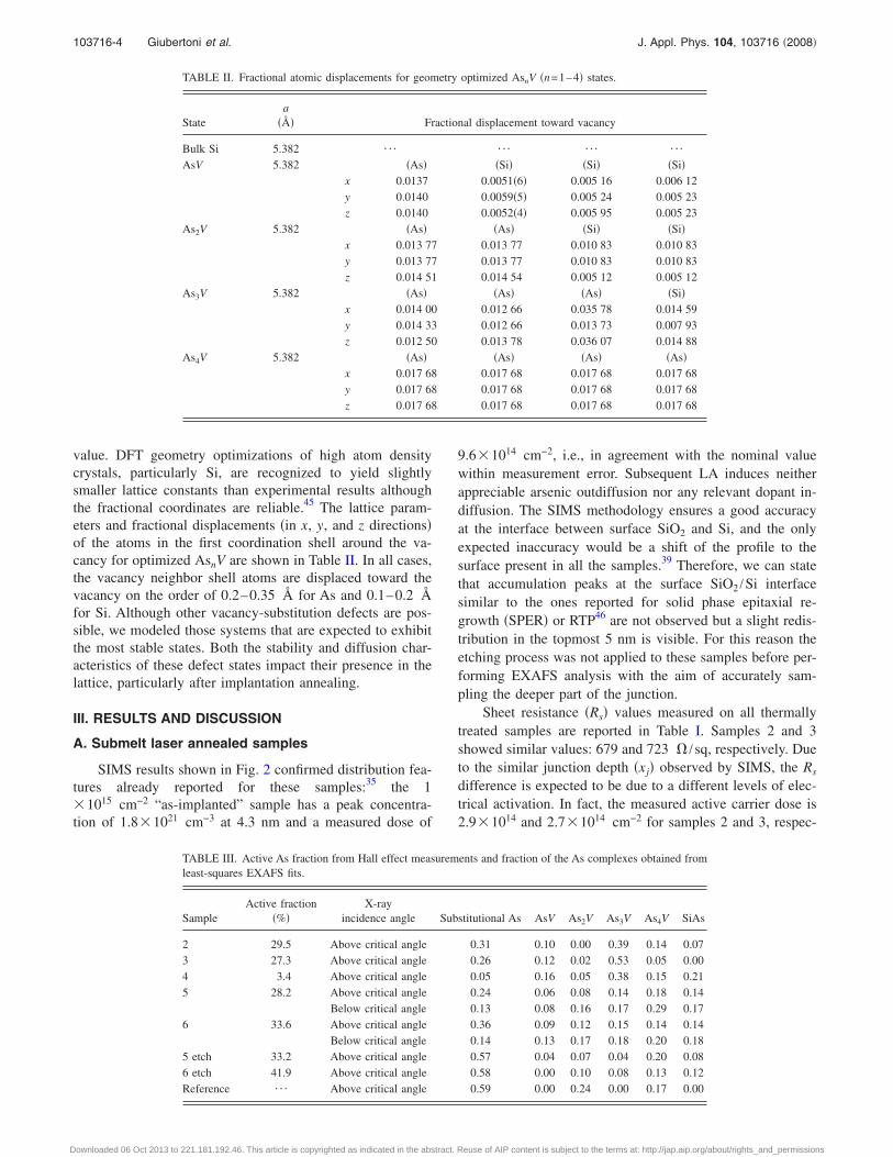
value. DFT geometry optimizations of high atom densitycrystals, particularly Si, are recognized to yield slightlysmaller lattice constants than experimental results althoughthe fractional coordinates are reliable.45 The lattice param-eters and fractional displacements �in x, y, and z directions�of the atoms in the first coordination shell around the va-cancy for optimized AsnV are shown in Table II. In all cases,the vacancy neighbor shell atoms are displaced toward thevacancy on the order of 0.2–0.35 Å for As and 0.1–0.2 Åfor Si. Although other vacancy-substitution defects are pos-sible, we modeled those systems that are expected to exhibitthe most stable states. Both the stability and diffusion char-acteristics of these defect states impact their presence in thelattice, particularly after implantation annealing.
III. RESULTS AND DISCUSSION
A. Submelt laser annealed samples
SIMS results shown in Fig. 2 confirmed distribution fea-tures already reported for these samples:35 the 1�1015 cm−2 “as-implanted” sample has a peak concentra-tion of 1.8�1021 cm−3 at 4.3 nm and a measured dose of
9.6�1014 cm−2, i.e., in agreement with the nominal valuewithin measurement error. Subsequent LA induces neitherappreciable arsenic outdiffusion nor any relevant dopant in-diffusion. The SIMS methodology ensures a good accuracyat the interface between surface SiO2 and Si, and the onlyexpected inaccuracy would be a shift of the profile to thesurface present in all the samples.39 Therefore, we can statethat accumulation peaks at the surface SiO2 /Si interfacesimilar to the ones reported for solid phase epitaxial re-growth �SPER� or RTP46 are not observed but a slight redis-tribution in the topmost 5 nm is visible. For this reason theetching process was not applied to these samples before per-forming EXAFS analysis with the aim of accurately sam-pling the deeper part of the junction.
Sheet resistance �Rs� values measured on all thermallytreated samples are reported in Table I. Samples 2 and 3showed similar values: 679 and 723 � /sq, respectively. Dueto the similar junction depth �xj� observed by SIMS, the Rs
difference is expected to be due to a different levels of elec-trical activation. In fact, the measured active carrier dose is2.9�1014 and 2.7�1014 cm−2 for samples 2 and 3, respec-
TABLE II. Fractional atomic displacements for geometry optimized AsnV �n=1–4� states.
Statea
�� Fractional displacement toward vacancy
Bulk Si 5.382 ¯ ¯ ¯ ¯
AsV 5.382 �As� �Si� �Si� �Si�x 0.0137 0.0051�6� 0.005 16 0.006 12y 0.0140 0.0059�5� 0.005 24 0.005 23z 0.0140 0.0052�4� 0.005 95 0.005 23
As2V 5.382 �As� �As� �Si� �Si�x 0.013 77 0.013 77 0.010 83 0.010 83y 0.013 77 0.013 77 0.010 83 0.010 83z 0.014 51 0.014 54 0.005 12 0.005 12
As3V 5.382 �As� �As� �As� �Si�x 0.014 00 0.012 66 0.035 78 0.014 59y 0.014 33 0.012 66 0.013 73 0.007 93z 0.012 50 0.013 78 0.036 07 0.014 88
As4V 5.382 �As� �As� �As� �As�x 0.017 68 0.017 68 0.017 68 0.017 68y 0.017 68 0.017 68 0.017 68 0.017 68z 0.017 68 0.017 68 0.017 68 0.017 68
TABLE III. Active As fraction from Hall effect measurements and fraction of the As complexes obtained fromleast-squares EXAFS fits.
SampleActive fraction
�%�X-ray
incidence angle Substitutional As AsV As2V As3V As4V SiAs
2 29.5 Above critical angle 0.31 0.10 0.00 0.39 0.14 0.073 27.3 Above critical angle 0.26 0.12 0.02 0.53 0.05 0.004 3.4 Above critical angle 0.05 0.16 0.05 0.38 0.15 0.215 28.2 Above critical angle 0.24 0.06 0.08 0.14 0.18 0.14
Below critical angle 0.13 0.08 0.16 0.17 0.29 0.176 33.6 Above critical angle 0.36 0.09 0.12 0.15 0.14 0.14
Below critical angle 0.14 0.13 0.17 0.18 0.20 0.185 etch 33.2 Above critical angle 0.57 0.04 0.07 0.04 0.20 0.086 etch 41.9 Above critical angle 0.58 0.00 0.10 0.08 0.13 0.12Reference ¯ Above critical angle 0.59 0.00 0.24 0.00 0.17 0.00
103716-4 Giubertoni et al. J. Appl. Phys. 104, 103716 �2008�
Downloaded 06 Oct 2013 to 221.181.192.46. This article is copyrighted as indicated in the abstract. Reuse of AIP content is subject to the terms at: http://jap.aip.org/about/rights_and_permissions
tively. When the implanted fluence is increased to 3�1015 cm−2 the Rs value also appeared to increase to782 � /sq and the active carrier dose decreased to just 9.1�1013 cm−2, indicating poorer electrical activation. Due tothe accuracy of the SIMS results, the ratio of the Hall effectmeasured active dose to the SIMS determined dose gives arelatively reliable measure of the active fraction of dopant inthe junction: this value, reported in Table I, is nearly onethird for the 1�1015 cm−2 samples, whereas it falls to �3%for the 3�1015 cm−2 sample. EXAFS was thus used to in-vestigate the amount of As in substitutional position and tounderstand defects behind the relatively large fractions ofinactive dopant. Only AsnV clusters and SiAs precipitateswere incorporated in the EXAFS fits together with the sub-stitutional arsenic. As discussed before, AsnV complexes arenot the only possible As clusters according to theoreticalstudies but most likely ones due to lower formation energies.Not only the formation energies but also the diffusion char-acteristics of different clusters have important effects on thepresence of these structures after postimplantationannealing.21,22 For AsnV clusters, the local structural param-eters obtained from geometry optimization calculations wereused in modeling of the EXAFS functions that were used inthe least-squares fits. For the monoclinic SiAs, EXAFS mod-eling the structural parameters from literature was used47 andfor the substitutional As form, EXAFS model was calculatedwith arsenic core atom replacing one of the Si atom in asilicon crystal.
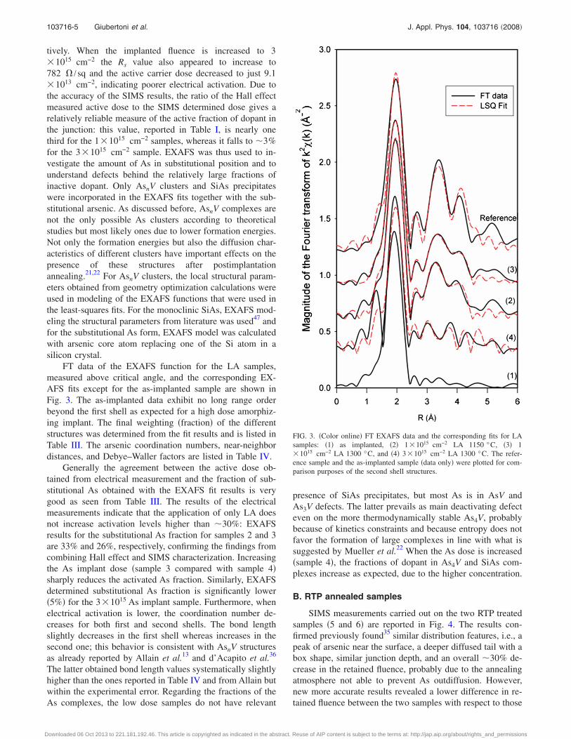
FT data of the EXAFS function for the LA samples,measured above critical angle, and the corresponding EX-AFS fits except for the as-implanted sample are shown inFig. 3. The as-implanted data exhibit no long range orderbeyond the first shell as expected for a high dose amorphiz-ing implant. The final weighting �fraction� of the differentstructures was determined from the fit results and is listed inTable III. The arsenic coordination numbers, near-neighbordistances, and Debye–Waller factors are listed in Table IV.
Generally the agreement between the active dose ob-tained from electrical measurement and the fraction of sub-stitutional As obtained with the EXAFS fit results is verygood as seen from Table III. The results of the electricalmeasurements indicate that the application of only LA doesnot increase activation levels higher than �30%: EXAFSresults for the substitutional As fraction for samples 2 and 3are 33% and 26%, respectively, confirming the findings fromcombining Hall effect and SIMS characterization. Increasingthe As implant dose �sample 3 compared with sample 4�sharply reduces the activated As fraction. Similarly, EXAFSdetermined substitutional As fraction is significantly lower�5%� for the 3�1015 As implant sample. Furthermore, whenelectrical activation is lower, the coordination number de-creases for both first and second shells. The bond lengthslightly decreases in the first shell whereas increases in thesecond one; this behavior is consistent with AsnV structuresas already reported by Allain et al.13 and d’Acapito et al.36
The latter obtained bond length values systematically slightlyhigher than the ones reported in Table IV and from Allain butwithin the experimental error. Regarding the fractions of theAs complexes, the low dose samples do not have relevant
presence of SiAs precipitates, but most As is in AsV andAs3V defects. The latter prevails as main deactivating defecteven on the more thermodynamically stable As4V, probablybecause of kinetics constraints and because entropy does notfavor the formation of large complexes in line with what issuggested by Mueller et al.22 When the As dose is increased�sample 4�, the fractions of dopant in As4V and SiAs com-plexes increase as expected, due to the higher concentration.
B. RTP annealed samples
SIMS measurements carried out on the two RTP treatedsamples �5 and 6� are reported in Fig. 4. The results con-firmed previously found35 similar distribution features, i.e., apeak of arsenic near the surface, a deeper diffused tail with abox shape, similar junction depth, and an overall �30% de-crease in the retained fluence, probably due to the annealingatmosphere not able to prevent As outdiffusion. However,new more accurate results revealed a lower difference in re-tained fluence between the two samples with respect to those
FIG. 3. �Color online� FT EXAFS data and the corresponding fits for LAsamples: �1� as implanted, �2� 1�1015 cm−2 LA 1150 °C, �3� 1�1015 cm−2 LA 1300 °C, and �4� 3�1015 cm−2 LA 1300 °C. The refer-ence sample and the as-implanted sample �data only� were plotted for com-parison purposes of the second shell structures.
103716-5 Giubertoni et al. J. Appl. Phys. 104, 103716 �2008�
Downloaded 06 Oct 2013 to 221.181.192.46. This article is copyrighted as indicated in the abstract. Reuse of AIP content is subject to the terms at: http://jap.aip.org/about/rights_and_permissions

previously reported, i.e., 7.0�1014 and 6.6�1014 cm−2 forsamples 5 and 6, respectively. In the Hall effect results, TableI, a higher Rs value is measured for sample 5 �RTP� com-pared to sample 6 �laser and RTP�, 490 against 450 � /sq,respectively. The active carrier fluence, however, is higherfor sample 6, 2.2�1014 against 2.0�1014 of sample 5. Con-sequently, the determined active dose fraction is 28% and34% for samples 5 and 6, respectively. This is coherent withthe difference in Rs values, given the same junction depth forthe two samples.
The accumulation of As below the surface oxide follow-ing RTP or SPER annealing is well known in literature.38,46,48
This arsenic accumulation is often constituted of As in eithera disordered form or in SiAs precipitates,10,37 and it canhinder the probing of the deeper part of the junction in anx-ray absorption experiment using grazing incidence.35
Therefore, the etching process was tested on these samples asdescribed in Sec. II. SIMS profiles obtained on the etchedsamples are reported in Fig. 4, shifted by 2.8 and 4.0 nm,respectively, in order to match the As tail.
FT of EXAFS function for these samples together withthe relative fits are depicted in Fig. 5 for measurements car-ried out above and below critical angle for the unetchedsamples, only above critical angle for the etched ones. Theresults of the analysis are summarized in Tables III and IV.
All the measurements revealed very similar values for num-ber of coordination and bond length in the first and secondshells between samples 5 and 6: The absolute values forbond length reproduce the ones obtained by Allain et al.13 onAs distributions with similar coordination number in the firstshell, whereas they are systematically lower than the morerecently published by d’Acapito et al.36 This discrepancy
TABLE IV. Coordination numbers, near-neighbor distances, and Debye–Waller factors from EXAFS fits.
Sample ID X-ray incidence angle
First shell Second shell
NR
���
�Å2� N�
R��
��Å2�
2 Above critical angle 3.7�2� 2.38�2� 0.002�1� 10.8�4� 3.85�2� 0.04�1�3 Above critical angle 3.6�2� 2.37�2� 0.002�1� 11.3�3� 3.87�2� 0.03�1�4 Above critical angle 3.3�2� 2.36�2� 0.004�2� 9.9�4� 3.88�2� 0.05�3�5 Above critical angle 3.7�3� 2.38�2� 0.003�2� 10.6�3� 3.86�2� 0.04�2�
Below critical angle 3.4�3� 2.35�1� 0.003�2� 10.3�4� 3.87�1� 0.03�2�6 Above critical angle 3.6�3� 2.38�2� 0.002�1� 10.6�3� 3.85�2� 0.02�2�
Below critical angle 3.5�2� 2.36�1� 0.003�1� 10.2�4� 3.88�2� 0.04�2�5 etch Above critical angle 3.8�2� 2.39�2� 0.002�1� 11.5�2� 3.85�1� 0.03�2�6 etch Above critical angle 3.8�2� 2.39�2� 0.002�1� 11.4�2� 3.85�1� 0.03�2�Reference Above critical angle 3.9�1� 2.40�1� 0.002�1� 11.6�2� 3.84�1� 0.02�1�
FIG. 4. �Color online� Arsenic SIMS profiles before and after etch forsamples with RTP and LA followed by RTP. The etched sample SIMS pro-files were rigidly shifted to match the As tail as depicted in the figure inorder to know how much As was removed.
FIG. 5. �Color online� FT EXAFS data for the RTP and the LA+RTPsample. �5� 1�1015 cm−2 RTP 1050 °C. �6� 1�1015 cm−2 LA 1150 °C+RTP 1050 °C. FT data for the etched samples, and above and below criti-cal angle measurements, were shown with the reference samples for com-parison purposes.
103716-6 Giubertoni et al. J. Appl. Phys. 104, 103716 �2008�
Downloaded 06 Oct 2013 to 221.181.192.46. This article is copyrighted as indicated in the abstract. Reuse of AIP content is subject to the terms at: http://jap.aip.org/about/rights_and_permissions

might be due to differences in the implant energies used inthis work �2 keV� and the ones used in the work of d’Acapitoet al.36 �5 keV�. In the lower energy implants one wouldexpect to have a higher As peak concentration close to sur-face where the near neighbor distances tend to go to lowervalues.14,37
However, when probing the topmost layer with an inci-dent angle below critical, coordination number and bondlength of the first shell decrease compared to the above criti-cal angle results as well as to the values observed on the onlyLA samples. This would denote a higher presence of vacan-cies near As atoms and thus a poorer substitutionality. On theother hand, when etched samples are analyzed, those param-eters are very close to the ones obtained on the highly acti-vated reference.
Regarding the fraction of As in the different complexes,the higher values for the substitutional As fraction have beenfound for sample 6, to which both LA and RTP have beenapplied, in agreement with the Hall effect result. Further-more, in measurements carried out at primary beam inci-dence below the critical angle, the As substitutional fractionfalls to �13% for both samples, indicating that the As in thetopmost layer is mostly off lattice sites. On the other hand,when the etched samples are probed, the same fraction in-creases to �60%. If this factor is applied to the total retaineddoses as measured by SIMS ��3.1�1014 cm−2 for bothsamples�, the total As in substitutional position is 1.8�1014 cm−2, that is nearly the same as that measured abovecritical angle �probing the whole dopant distribution� onsample 5 �1.7�1014 cm−2� and slightly less than sample 6�2.4�1014 cm−2�, probably because the latter was etchedmore than sample 5. This means that the active dopant ismainly located in the box-shaped tail, whereas in the accu-mulation close to the surface �top 2.5 nm�, where As concen-tration is high ��2�1021 cm−3�, the clustering and precipi-tation of As are expected. In fact, the fraction of As in thedeactivating defects AsnV and SiAs increases when samplesare probed below critical angles, especially As3V, As4V, andSiAs. The As4V and SiAs population is higher than what isobserved in the LA 1�1015 cm−2 samples. This is argued tobe due to the higher As concentration created at the surfaceby the RTP induced diffusion. Moreover, the same effectmoved dopant atoms, favoring the formation of more stablecomplexes and overcoming the kinetics constraints. On theother hand, in the etched samples, all the AsnV complex frac-tions are very low except for As4V and SiAs ones. In anycase, in absolute values, the latter corresponds to 3–6�1013 As /cm−2, i.e., just �40% of what is observed in thesurface layer. The biggest discrepancy between Hall effectactive fraction and EXAFS determined As substitutionalfraction was found on the etched samples. The reason isunder investigation at the moment, but it can be supposed tobe related to artifacts induced by the etching process.
A detailed investigation on the correlation between vari-ous heat treatments and EXAFS determined fractions of theAs clusters and the correlation between the theoretically cal-culated parameters �such as formation energies and diffusionproperties� will be performed in the future.
IV. CONCLUSION
Electrically active As concentration and local structurearound the As atom have shown good correlation in a seriesof As implants in Si subjected to various postimplantationheat treatments. The As atoms were implanted at an energyof 2 keV with doses between 1�1015 and 3�1015 cm−2,and then annealed by either laser submelting treatment orRTP. The active carrier concentration from Hall effect mea-surements was correlated with the substitutional As deter-mined by the EXAFS least-squares fits performed by usingDFT calculated theoretical standards for the AsnV clusterforms and monoclinic SiAs precipitates. Fractions of theSiAs precipitates and the other AsnV clusters were deter-mined from the EXAFS results. A strong correlation wasobserved between the EXAFS results and the electrical re-sults in terms of active carrier concentration and the substi-tutional As. The only laser treatment produced less than athird of active As on the 1�1015 cm−2 samples. The �70%inactive dopant is mainly confined in As3V complexes asexpected from theoretical considerations. In fact, the As4Vcomplex is more stable but kinetics constraints hinder itsformation. However, when the As dose is increased to 3�1015 cm−2 the electrically active fraction falls to less than5% and As is found also in As4V and SiAs precipitates. RTPprocessing induced a relevant As indiffusion and an accumu-lation of As in a thin layer below the surface oxide. Thecombined use of results obtained by varying primary x-raybeam angle and using a surface etched sample enabled us toconclude that 24% of the As implanted dose is essentiallyconfined below the surface accumulation. The latter ismainly formed by As3V, As4V, and SiAs complexes. LAfollowed by RTP led to pronounced As atom redistribution,resulting also in the highest active carrier concentration�34%� as determined from electrical measurements. EXAFSresults indicated 36% of substitutional As for the samesample.
ACKNOWLEDGMENTS
The authors would like to acknowledge Francescod’Acapito, INFM, and ESRF Grenoble for support and dis-cussion during EXAFS analysis session, Silvia Milita, CNR-IMM Bologna for providing reference sample and helpingduring EXAFS analysis, and Justin Hamilton and Jim Sharp,University of Surrey for characterizing some samples by HallEffect measurements. The work of M.A.S. is supported byResearch Corporation Award No. CC6405 and NSF GrantNo. DMI 0420952. We acknowledge the support of the Eu-ropean Commission under the action �Structuring the Euro-pean Research Area’. NIST disclaimer: Certain commercialequipment, instruments, or materials are identified in thisdocument. Such identification does not imply recommenda-tion or endorsement by the National Institute of Standardsand Technology, nor does it imply that the products identifiedare necessarily the best available for the purpose.
1R. Duffy, T. Dao, Y. Tamminga, K. van der Tak, F. Roozeboom, and E.Augendre, Appl. Phys. Lett. 89, 071915 �2006�.
2R. O. Schwenker, E. S. Pan, and R. F. Lever, J. Appl. Phys. 42, 3195�1971�.
103716-7 Giubertoni et al. J. Appl. Phys. 104, 103716 �2008�
Downloaded 06 Oct 2013 to 221.181.192.46. This article is copyrighted as indicated in the abstract. Reuse of AIP content is subject to the terms at: http://jap.aip.org/about/rights_and_permissions

3A. Lietoila, J. F. Gibbons, T. J. Magee, J. Peng, and J. D. Hong, Appl.Phys. Lett. 35, 532 �1979�.
4D. Nobili, S. Solmi, A. Parisini, M. Derdour, A. Armigliato, and L. Moro,Phys. Rev. B 49, 2477 �1994�.
5A. Lietoila, J. F. Gibbons, and T. W. Sigmon, Appl. Phys. Lett. 36, 765�1980�.
6C. Brizard, J. R. Regnard, J. L. Allain, A. Bourret, M. Dubus, A. Ar-migliato, and A. Parisini, J. Appl. Phys. 75, 126 �1994�.
7A. Satta, E. Albertazzi, G. Lulli, and L. Colombo, Phys. Rev. B 72,235206 �2005�.
8A. Herrera-Gomez, P. M. Rousseau, G. Materlik, T. Kendelewicz, J. C.Woicik, P. B. Griffin, J. Plummer, and W. E. Spicer, Appl. Phys. Lett. 68,3090 �1996�.
9A. Herrera-Gómez, P. M. Rousseau, J. C. Woicik, T. Kendelewicz, J.Plummer, and W. E. Spicer, J. Appl. Phys. 85, 1429 �1999�.
10A. Parisini, A. Bourret, A. Armigliato, M. Servidori, S. Solmi, R. Fabbri,J. R. Regnard, and J. L. Allain, J. Appl. Phys. 67, 2320 �1990�.
11O. Dokumaci, P. M. Rousseau, S. Luning, V. Krishnamoorthy, K. S. Jones,and M. E. Law, J. Appl. Phys. 78, 828 �1995�.
12K. C. Pandey, A. Erbil, G. S. Cargill III, R. F. Boehme, and D. Vanderbilt,Phys. Rev. Lett. 61, 1282 �1988�.
13J. L. Allain, J. R. Regnard, A. Bourret, A. Parisini, A. Armigliato, G.Tourillon, and S. Pizzini, Phys. Rev. B 46, 9434 �1992�.
14M. A. Sahiner, S. W. Novak, J. Woicik, J. Liu, and V. Krishnamoorthy,IEEE Transactions Ion Implantation Technology, 2000 �unpublished�, Vol.00EX432, p. 600.
15P. M. Rousseau, P. B. Griffin, and J. D. Plummer, Appl. Phys. Lett. 65,578 �1994�.
16P. M. Rousseau, P. B. Griffin, W. T. Fang, and J. D. Plummer, J. Appl.Phys. 84, 3593 �1998�.
17D. W. Lawther, U. Myler, P. J. Simpson, P. M. Rousseau, P. B. Griffin, andJ. D. Plummer, Appl. Phys. Lett. 67, 3575 �1995�.
18U. Myler, P. J. Simpson, D. W. Lawther, and P. M. Rousseau, J. Vac. Sci.Technol. B 15, 757 �1997�.
19K. Saarinen, J. Nissila, H. Kauppinen, M. Hakala, M. J. Puska, P. Hauto-jarvi, and C. Corbel, Phys. Rev. Lett. 82, 1883 �1999�.
20V. Ranki, A. Pelli, and K. Saarinen, Phys. Rev. B 69, 115205 �2004�.21M. Ramamoorthy and S. T. Pantelides, Phys. Rev. Lett. 76, 4753 �1996�.22D. C. Mueller, E. Alonso, and W. Fichtner, Phys. Rev. B 68, 045208
�2003�.23D. Mathiot and J. C. Pfister, Appl. Phys. Lett. 42, 1043 �1983�.24J. Xie and S. P. Chen, Phys. Rev. Lett. 83, 1795 �1999�.25D. J. Chadi, P. H. Citrin, C. H. Park, D. L. Adler, M. A. Marcus, and H.-J.
Gossman, Phys. Rev. Lett. 79, 4834 �1997�.26P. M. Voyles, D. J. Chadi, P. H. Citrin, D. A. Muller, J. L. Grazul, P. A.
Northrup, and H.-J. L. Gossmann, Phys. Rev. Lett. 91, 125505 �2003�.27S. A. Harrison, T. F. Edgar, and G. S. Hwang, Appl. Phys. Lett. 87,
231905 �2005�.28S. A. Harrison, T. F. Edgar, and G. S. Hwang, Phys. Rev. B 74, 195202
�2006�.29S. A. Harrison, T. F. Edgar, and G. S. Hwang, Appl. Phys. Lett. 85, 4935
�2004�.30R. Brindos, P. Keys, K. S. Jones, and M. E. Law, Appl. Phys. Lett. 75, 229
�1999�.31R. Kim, T. Hirose, T. Shano, H. Tsuji, and K. Taniguchi, Jpn. J. Appl.
Phys., Part 1 41, 227 �2002�.32S. Solmi, M. Ferri, M. Bersani, D. Giubertoni, and V. Soncini, J. Appl.
Phys. 94, 4950 �2003�.33N. Kong, S. K. Banerjee, T. A. Kirichenko, S. G. H. Anderson, and M. C.
Foisy, Appl. Phys. Lett. 90, 062107 �2007�.34N. Kong, T. A. Kirichenko, Y. Kim, M. C. Foisy, and S. K. Banerjee, J.
Appl. Phys. 104, 013514 �2008�.35D. Giubertoni, G. Pepponi, M. Bersani, S. Gennaro, F. D’Acapito, R.
Doherty, and M. A. Foad, Nucl. Instrum. Methods Phys. Res. B 253, 9�2006�.
36F. d’Acapito, S. Milita, A. Satta, and L. Colombo, J. Appl. Phys. 102,043524 �2007�.
37A. Terrasi, E. Rimini, V. Raineri, F. Iacona, F. La Via, S. Colonna, and S.Mobilio, Appl. Phys. Lett. 73, 2633 �1998�.
38R. Kasnavi, Y. Sun, R. Mo, P. Pianetta, P. B. Griffin, and J. D. Plummer,J. Appl. Phys. 87, 2255 �2000�.
39D. Giubertoni, M. Bersani, M. Barozzi, S. Pederzoli, E. Iacob, J. A. vanden Berg, and M. Werner, Appl. Surf. Sci. 252, 7214 �2006�.
40G. Pepponi, D. Giubertoni, S. Gennaro, M. Bersani, M. Anderle, R.Grisenti, M. Werner, and J. A. van den Berg, in Ion Implantation Technol-ogy, Marseille, France, edited by K. J. Kirkby, R. Gwilliam, A. Smith, andD. Chivers �AIP, New York, 2006�, Vol.117.
41A. L. Ankudinov, B. Ravel, J. J. Rehr, and S. D. Conradson, Phys. Rev. B58, 7565 �1998�.
42M. Newville, P. Livins, Y. Yacoby, J. J. Rehr, and E. A. Stern, Phys. Rev.B 47, 14126 �1993�.
43M. D. Segall, P. J. D. Lindan, M. J. Probert, C. J. Pickard, P. J. Hasnip, S.J. Clark, and M. C. Payne J. Phys.: Condens. Matter 14, 2717 �2002�.
44J. P. Perdew and Y. Wang, Phys. Rev. B 45, 13244 �1992�.45C. Skylaris and P. D. Haynes, J. Chem. Phys. 127, 164712 �2007�.46A. Parisini, V. Morandi, S. Solmi, P. G. Merli, D. Giubertoni, M. Bersani,
and J. A. van den Berg, Appl. Phys. Lett. 92, 261907 �2008�.47T. Wadsten, Acta Chem. Scand. 19, 1232 �1965�.48K. Suzuki, Y. Kataoka, S. Nagayama, C. W. Magee, T. H. Buyuklimanli,
and T. Nagayama, IEEE Trans. Electron Devices 54, 262 �2007�.
103716-8 Giubertoni et al. J. Appl. Phys. 104, 103716 �2008�
Downloaded 06 Oct 2013 to 221.181.192.46. This article is copyrighted as indicated in the abstract. Reuse of AIP content is subject to the terms at: http://jap.aip.org/about/rights_and_permissions