
Magnetic Tunnel Junctions and Superconductor/Ferromagnet ...
101
-
Upload
khangminh22 -
Category
Documents
-
view
0 -
download
0
Transcript of Magnetic Tunnel Junctions and Superconductor/Ferromagnet ...

Magnetic Tunnel Junctions andSuperconductor/Ferromagnet Hybrids
Investigated by Low-Temperature ScanningLaser Microscopy
Dissertationder Mathematisch-Naturwissenschaftlichen Fakultät
der Eberhard Karls Universität Tübingenzur Erlangung des Grades einesDoktors der Naturwissenschaften
(Dr. rer. nat.)
vorgelegt vonRobert Werneraus Laupheim
Tübingen2011

Tag der mündlichen Qualikation: 1. Februar 2012Dekan: Prof. Dr. Wolfgang Rosenstiel1. Berichterstatter: Prof. Dr. Dieter Kölle2. Berichterstatter: Prof. Dr. Reinhold Kleiner

Abstract
Low-temperature scanning laser microscopy (LTSLM) allows the investigation of lo-cal properties in thin lm structures in a broad temperature range. Depending onthe sample under investigation, LTSLM can map various kinds of physical proper-ties such as the current distribution or the magnetic microstructure. In this thesis,the correlation between local and integral magnetotransport properties in thin-lmsuperconductor/ferromagnet (S/F) hybrids and magnetic tunnel junctions are in-vestigated.In S/F hybrids composed of Pb/BaFe12O19, we studied experimentally the eectof the stripe like domain structure of the BaFe12O19 substrate on the magnetore-sistance of superconducting Pb microbridges. A thin insulating layer between Pband the ferromagnet ensures pure electromagnetic coupling between the antagonis-tic phenomena of singlet superconductivity and ferromagnetism. Two bridges withdierent orientation with respect to the stripe-like domain walls (parallel and per-pendicular) were probed by LTSLM. In this technique, the sample is locally heatedin the thin lm (x, y) plane by a laser beam, which can induce a detectable voltagechange ∆V (x, y), depending on the physical properties of the heated area. Theresulting voltage images can visualize various physical properties, depending on theinvestigated sample. Direct verication of the formation of inhomogeneous super-conducting states in the Pb bridges, induced by the inhomogeneous stray eld ofthe ferromagnet and their manipulation by an external magnetic eld were obtainedby LTSLM. In particular, the localized state of domain-wall superconductivity wasvisualized in a sample where exactly one domain wall is running along the center ofthe Pb bridge, inducing a superconducting path for the current. Another state oflocalized superconductivity, called edge superconductivity, was probed in Nb micro-bridges. In an external magnetic eld applied perpendicular to the sample surface,superconductivity survives at the edges even for elds larger than the upper criticaleld Hc2 for bulk superconductivity.The interaction between superconductivity and ferromagnetism was also studied inheteroepitaxially grown bilayers composed of ferromagnetic La0.7Ca0.3MnO3 on topof superconducting YBa2Cu3O7 (YBCO). The focus was on transport properties aswell as on magnetic ordering and orbital occupation at the interface. We found, thata signicant reduction of the superconducting transition temperature Tc of singleYBCO thin lms occurs only for a layer thickness below 10 nm. The suppression ofTc in the bilayers was only slightly stronger compared to single YBCO lms. Ourx-ray magnetic circular dichroism measurements conrm recently published data ofan induced magnetic moment on the interfacial Cu by the ferromagnetically orderedMn ions. However, we observe a signicantly larger Cu moment than previouslyreported, indicating stronger coupling between Cu and Mn at the interface. Thiscan explain the reduced suppression of Tc in our samples.Magnetic tunnel junctions (MTJs) were investigated by LTSLM to correlate integralmagnetotransport measurements with local sample properties. We have performedresistance versus magnetic eld measurements for a MTJ based on La0.65Sr0.35MnO3
(LSMO) with SrTiO3 barrier, grown by molecular-beam epitaxy. Magnetoresistancemeasurements show a large eld window of extremely high tunneling magnetoresis-

tance (TMR) at low temperature which reached about 1900 %. This is the highestTMR value reported so far. Assuming identical interfaces, this TMR ratio corre-sponds to an interfacial spin polarization of ∼ 95 %. Studies with LTSLM allow thedetermination of the local relative magnetization orientation of the two electrodesas a function of magnitude and orientation of the external magnetic eld. Sweepingthe eld amplitude at xed orientation revealed magnetic domain nucleation andpropagation in the junction electrodes. The results show that LTSLM can be usedto link the magnetic microstructure to the integral magnetotransport properties andthus provides a valuable tool for further investigations of MTJs. Moreover, the ob-tained information on the relative magnetization orientation could not be obtainedby any other imaging technique, so far.

Kurzfassung
Die Tieftemperatur-Rasterlasermikroskopie (TTRLM) ermöglicht die Untersuchunglokaler Eigenschaften von Dünnlmstrukturen in einem breiten Temperaturbereich.Abhängig von der untersuchten Probe lassen sich durch die TTRLM verschiedenstephysikalische Eigenschaften wie zum Beispiel die Stromverteilung oder die mag-netische Mikrostruktur abbilden. In dieser Arbeit wird die Beziehung zwischenlokalen und integralen Magnetotransport-Eigenschaften von Dünnlmstrukturen ausSupraleiter/Ferromagnet Hybriden und magnetischen Tunnelkontakten untersucht.In S/F Hybriden aus Pb/BaFe12O19 wurde experimentell der Eekt der ferromag-netischen Streifendomänen des BaFe12O19 Substrates auf den Magnetowiderstandvon supraleitenden Pb Brücken untersucht. Eine dünne isolierende Schicht zwis-chen Pb und dem Ferromagnet garantiert eine rein elektromagnetische Wechsel-wirkung zwischen den gegensätzlichen Phänomenen von Spin-Singulett Supraleitungund Ferromagnetismus. Es wurden zwei Brücken mit unterschiedlicher Orientierungbezüglich der streifenartigen Domänen (parallel oder senkrecht) mittels TTRLM un-tersucht. Bei dieser Technik wird die Probe lokal in der Filmebene (x, y) mit einemLaser erwärmt. Je nach Eigenschaft der bestrahlten Fläche kann dies zu einer mess-baren Spannungsänderung ∆V (x, y) führen. Die dabei entstehenden Spannungs-bilder können verschiedenste physikalische Eigenschaften abbilden. Mit Hilfe derTTRLM konnte ein direkter Nachweis von Zuständen inhomogener Supraleitung inden Pb Brücken erbracht werden. Desweiteren konnte gezeigt werden, dass sich dieZustände durch ein externes Magnetfeld manipulieren lassen. Insbesondere wurdeder Zustand der Domänenwandsupraleitung in einer Brücke abgebildet, in der genaueine einzige Domänenwand entlang der Mitte der Brücke verläuft und welche einenals supraleitenden Pfad für den Strom induziert. Ein weiterer Zustand lokalisierterSupraleitung wurde in Nb Brücken untersucht, die sogenannte Randsupraleitung.Dabei existiert die Supraleitung an den Probenrändern in einem externen Mag-netfeld senkrecht zur Probenoberäche, auch wenn das Feld gröÿer als das oberekritische Feld Hc2 ist.Die Wechselwirkung von Supraleitung und Ferromagnetismus wurde auch in het-eroepitaktisch gewachsenen Bilagen aus ferromagnetischem La0.7Ca0.3MnO3 undsupraleitendem YBa2Cu3O7 (YBCO) untersucht. Dabei lag der Schwerpunkt aufden Transporteigenschaften sowie der magnetischen Ordnung und den elektronis-chen Eigenschaften an der Grenzäche. Eine deutliche Unterdrückung der kritischenTemperatur Tc von YBCO Dünnlmen trat erst unterhalb einer Dicke von 10 nm auf.In Bilagen war die Unterdrückung im Vergleich zu einzelnen YBCO Dünnlmen nuretwas stärker. Mit Hilfe von Röntgenabsorptionsspektroskopie mit zirkular polar-isierten Röntgenstrahlen konnten kürzlich erschienene Messungen eines induziertenmagnetischen Moments auf Cu Atomen durch die ferromagnetisch geordneten MnMomente an der Grenzäche bestätigt werden. Jedoch zeigte die vermessene Probeein deutlich stärkeres Cu Moment, was für eine stärkere Wechselwirkung an derGrenzäche spricht. Dies könnte die relativ geringe Unterdrückung von Tc in un-seren Proben erklären.Magnetische Tunnelkontakte (MTK) wurden mittels TTRLM untersucht um dielokalen und integralen Eigenschaft miteinander zu korrelieren. An La0.65Sr0.35MnO3

(LSMO) basierten MTK mit SrTiO3 Barriere wurden Widerstandsmessungen in Ab-hängigkeit vom äuÿeren Magnetfeld durchgeführt. Die LSMO/SrTiO3/LSMO Tri-lagen wurden mittels Molekularstrahlepitaxie gewachsen. Widerstandsmessungenin Abhängigkeit des äuÿeren Magnetfeldes zeigen einen groÿen Magnetfeldbereichmit sehr hohem Tunnelmagnetowiderstand (TMR), welcher bei tiefen Temperatureneinen Wert von bis zu ∼ 1900% erreicht. Dies ist bisher der höchste gemessene TMRWert überhaupt. Unter der Annahme von identischen Grenzächen ergibt sich da-raus eine Spinpolarisation an den Grenzächen von ungefähr 95%. Mit Hilfe derAbbildungen konnte lokal die relative Magnetisierung in Abhängigkeit von Richtungund Gröÿe des angelegten Magnetfeldes bestimmt werden. Beim Durchfahren desMagnetfeldes zeigen die Abbildungen die Bildung und die Ausbreitung von Domänenin den ferromagnetischen Elektroden. Die Ergebnisse zeigen, dass durch TTRLMeine Beziehung zwischen der lokalen magnetischen Struktur und den integralen Mag-netowiederstandskurven hergestellt werden kann. Darüber hinaus erhält man Infor-mation über die Verteilung der relativen Orientierung der Magnetisierung beiderElektroden, was bisher mit keiner anderen Abbildungstechnik möglich war.

List of publications
This is a cumulative thesis which is based on the publications listed below. Theyare referred to in the text by their roman numerals. The publications are attachedat the very end of the thesis.
Appended publications
I A.Yu. Aladyshkin, J. Fritzsche, R. Werner, R.B.G. Kramer, S.Guénon, R. Kleiner, D. Koelle and V.V. Moshchalkov,Crossover between dierent regimes of inhomogeneous superconduc-tivity in planar superconductor-ferromagnet hybrids,Phys. Rev. B 84, 094523 (2011)
II R. Werner, A.Yu. Aladyshkin, S. Guénon, J. Fritzsche, I.M. Nefe-dov, V.V. Moshchalkov, R. Kleiner and D. Koelle,Domain-wall and reverse-domain superconducting states of a Pbthin-lm bridge on a ferromagnetic BaFe12O19 single crystal,Phys. Rev. B 84, 020505(R) (2011)
III R. Werner, A. Yu. Aladyshkin, I. M. Nefedov, A. V. Putilov, M.Kemmler, D. Bothner, A. Loerincz, K. Ilin, M. Siegel, R. Kleiner,and D. Koelle,Edge superconductivity in Nb thin lm microbridges revealed by in-tegral and spatially resolved electric transport,submitted to Phys. Rev. B (2011), arXiv:1112.2256
IV R. Werner, C. Raisch, A. Ruosi, B. A. Davidson, P. Nagel, M.Merz, S. Schuppler, M. Glaser, J. Fujii, T. Chassé, R. Kleiner andD. Koelle, YBa2Cu3O7 / La0.7Ca0.3MnO3 bilayers: Interface cou-pling and electric transport properties,Phys. Rev. B 82, 224509 (2011)
V R. Werner, M. Weiler, A. Yu. Petrov, B. A. Davidson, R. Gross,R. Kleiner, S. T. B. Goennenwein and D. Koelle,Local Tunneling Magnetoresistance probed by Low-TemperatureScanning Laser Microscopy,App. Phys. Lett. 99, 182513 (2011)
VI R. Werner, A. Yu. Petrov, L. Alvarez Miño, R. Kleiner, D. Koelleand B. A. Davidson,Improved tunneling magnetoresistance at low temperature in man-ganite junctions grown by molecular beam epitaxy,App. Phys. Lett. 98, 162505 (2011)

Publications not included in this thesis
VII R. Werner, C. Raisch, V. Leca, V. Ion, S. Bals, G. Van Tendeloo,T. Chassé, R. Kleiner and D. Koelle,Transport, magnetic, and structural properties of La0.7Ce0.3MnO3
thin lms: Evidence for hole-doping,Phys. Rev. B 79, 054416 (2009)
VIII J. Nagel, K. B. Konovalenko, M. Kemmler, M. Turad, R. Werner,E. Kleisz, S. Menzel, R. Klingeler, B. Büchner, R. Kleiner and D.Koelle,Resistively shunted YBa2Cu3O7 grain boundary junctions and low-noise SQUIDs patterned by a focused ion beam down to 80 nmlinewidth,Supercond. Sci. Technol. 24, 015015 (2011)

Contents
Introduction 3
1 Superconductor/ferromagnet hybrids 71.1 Introduction . . . . . . . . . . . . . . . . . . . . . . . . . . . . . . . . 71.2 Inhomogeneous superconductivity . . . . . . . . . . . . . . . . . . . . 9
1.2.1 Introduction . . . . . . . . . . . . . . . . . . . . . . . . . . . . 91.2.2 Low-temperature scanning laser microscopy . . . . . . . . . . 111.2.3 Summary of pub. I: inhomogeneous superconducting states . . 111.2.4 Summary of pub. II: domain-wall superconductivity . . . . . . 121.2.5 Summary of pub. III: edge superconductivity . . . . . . . . . 12
1.3 Electrically coupled S/F oxide heterostructures . . . . . . . . . . . . 131.3.1 Introduction . . . . . . . . . . . . . . . . . . . . . . . . . . . . 131.3.2 Summary of pub. IV: YBCO/LCMO bilayers . . . . . . . . . 14
2 Magnetic tunnel junctions 172.1 Introduction . . . . . . . . . . . . . . . . . . . . . . . . . . . . . . . . 172.2 Magnetoresistance of LSMO based MTJs . . . . . . . . . . . . . . . . 19
2.2.1 Introduction . . . . . . . . . . . . . . . . . . . . . . . . . . . . 192.2.2 Summary of pub. V: TMR in LSMO based MTJ . . . . . . . 20
2.3 Visualization of local properties in a MTJ . . . . . . . . . . . . . . . 202.3.1 Introduction . . . . . . . . . . . . . . . . . . . . . . . . . . . . 202.3.2 Summary of pub. VI: local TMR probed by LTSLM . . . . . . 21
Bibliography 23
Appended publications 35

2

Introduction
Transition metal oxides with strong electron correlations form since many years anactive and constantly growing research eld of solid state physics.13 The interplay ofspin, charge and orbital degree of freedom leads to a number of dierent phenomenasuch as ferroelectricity, ferromagnetism, antiferromagnetism and superconductivity.4
In strongly correlated electron systems, interfacial properties can be crucial for themacroscopic behavior of the system and they can dier signicantly from those ofthe bulk compounds. This allows for the possibility to create new physical stateswhich do not exist in bulk compounds.5 The most prominent example of unexpectedinterface eects is the system LaAlO3/SrTiO3.6,7 Though both materials are insu-lators, a quasi-two dimensional electron liquid is formed at the interface which evenbecomes superconducting. Another possibility is the combination of oxide mate-rials with dierent ordering phenomena. Of special interest is the combination oftwo antagonistic phenomena such as superconductivity and ferromagnetism in anall oxide heterostructure.8,9 While superconductor/ferromagnet (S/F) hybrid struc-tures based on metallic ferromagnets and conventional superconductors have beeninvestigated in detail,10 there are much less studies on S/F systems involving oxidematerials.1114
Interface properties also determine the characteristics of many devices such as pn-junctions, metal-oxide-semiconductor eld-eect transistors or magnetic tunnel junc-tions (MTJs). In the latter one, the tunnel magnetoresistance (TMR) which is thegure of merit of MTJs, depends on the spin polarization at the interface.15 Thehigher the spin polarization, the higher the TMR ratio. It has been shown that theinterfacial spin polarization can be increased by the so-called interface engineering,where the doping prole is gradually changed at the interface.16,17 Beside that, im-proving the TMR ratio as well as the switching behavior needs investigations of theimpact of the magnetic microstructure on the integral magnetotransport properties.The domain structure is also crucial in electrically decoupled S/F hybrids where thestray eld of the ferromagnetic domains can lead to inhomogeneous superconduc-tivity, tunable by an external magnetic eld H.1822 This leads to a complex H − Tphase diagram with various dierent states of inhomogeneous superconductivity.While ngerprints of this inhomogeneous states have been found in magnetotrans-port measurements,19 a clear correlation between integral and local properties is stilllacking for most states22.Since many years, low-temperature scanning laser microscopy (LTSLM) is used tomap various kinds of physical properties such as the critical current or critical tem-perature distribution in superconducting thin lms or the magnetic domain struc-ture in ferromagnetic thin lms and to correlate them with integral transport mea-

4
surements.2224 Therefore, LTSLM seems to be a valuable technique, to visualizeinhomogeneous properties in S/F hybrids as well as in MTJs.In the framework of this thesis, the transport and interface properties of S/F hybridscomposed of YBa2Cu3O7 (YBCO) and La0.7Ca0.3MnO3 (LCMO) have been probed.Due to the similar crystal structure of these materials, it is possible to combinethe dierent ordering phenomena in epitaxial heterostructures with well denedinterfaces. The aim of our investigations was to improve the understanding of theinuence of LCMO on YBCO transport properties as well as the electronic andmagnetic properties at the interface.MTJs based on the half-metal oxide La0.65Sr0.35MnO3 (LSMO), grown by molecular-beam epitaxy (MBE), were investigated. LSMO has a Curie-temperature well aboveroom temperature and it is, due to its spin polarization of about 100 %, a promisingcandidate for high TMR ratios at room temperature. We used MBE, as it is thegrowth technique with the highest growth control on the atomic scale and it allowsto adjust the doping level at any time during the growth process. It is therefore themost suitable technique to realize MTJ with engineered interfaces. But rst, theidea was to grow and pattern reproducible MTJs and to probe the inuence of thelocal microstructure on the integral magnetotransport by LTSLM.The technique of LTSLM was also applied to electrically decoupled S/F hybridscomposed of Pb/BaFe12O19. Here we focused on the electrical characterization ofthe S/F hybrid and the visualization of inhomogeneous states of superconductivityat dierent positions in the H − T phase diagram, induced by the stray eld of thedomain structure in the ferromagnetic substrate. A correlation between local andintegral properties should be established. In these studies we included investigationson Nb microbridges, where we probed one particular case of inhomogeneous super-conductivity, localized at the samples edges.
This thesis is organized as follows:
The rst part of chapter 1, gives a general introduction to the eld of S/F systems,followed by a detailed overview on states of inhomogeneous superconductivity in elec-trically decoupled S/F hybrids and superconducting bridges in an external magneticeld. In the following, the signal mechanism of LTSLM which was used to investigatestates of inhomogeneous superconductivity is described. Subsequently, the most im-portant ndings of the publications dealing with inhomogeneous superconductivityare summarized. The next section gives an introduction to interface eects of elec-trically coupled YBCO/LCMO bilayers, followed by a summary of the main results.The content of chapter 2 are MTJs. The rst paragraph gives an introduction toMTJs and describes open issues in this eld. The paragraph thereafter summarizesthe main results of the electrical characterization of LSMO/SrTiO3/LSMO MTJs.The last section in this chapter summarized the investigations of local properties ofa MTJ by LTSLM. The publications on which this thesis is based on are attachedafter the bibliography.

5
a

6

Chapter 1
Superconductor/ferromagnet hybrids
This chapter presents investigations on superconductor/ferromagnet hybrids. Therst paragraph will briey introduce the interplay between ferromagnetism and su-perconductivity and motivate the research. In the framework of this thesis, vari-ous aspects of two superconductor/ferromagnet systems have been studied. Electrictransport and interface properties were investigated in YBa2Cu3O7/La0.7Ca0.3MnO3
bilayers with both materials in direct electrical contact, while in electrically decou-pled Pb/BaFe12O19 hybrids, the aim was the visualization of inhomogeneous super-conductivity. Although it is not an superconductor/ferromagnet hybrid, studies ofinhomogeneous superconductivity in Nb bridges are included in this chapter, as theycomplete the experiments on Pb/BaFe12O19 hybrids.
1.1 Introduction
Superconductivity and ferromagnetism are two ordering phenomena which have beeninvestigated in detail over the past decades. While, initially, both phenomena wereinvestigated separately, the interest in combining and exploring the interaction ofboth phenomena under various circumstances has been increasing in the last years.Ferromagnetism and superconductivity are two antagonistic phenomena, as ferro-magnets tends to align the electron spins parallel, due to the exchange interaction†,while the superconducting condensate is formed by Cooper-pairs (CPs) which con-sist of two electrons (or holes) with opposite spin orientation (spin-singlet state).These fundamental dierences make it very unlikely to nd the phenomena of spin-singlet superconductivity and long-ranged ferromagnetism (FM) in bulk materials.It should be noted, that beside the spin-singlet state (S = 0), CPs can also be in thespin-triplet state (S = 1), which leads to completely dierent interaction betweensuperconductivity and ferromagnetism. Only spin-singlet superconductivity will beconsidered in the following, if not stated otherwise.The interaction between both phenomena was rst considered by Ginzburg,26 whodescribed the suppression of superconductivity by a pure electromagnetic interactionwhich will be shortly described in the following. Besides the opposite spin alignment
†The exchange interaction is a quantum mechanical eect, based on the Pauli Principle and the
coulomb repulsion. For details see Blundell et al..25

8 Chapter 1. Superconductor/ferromagnet hybrids
in spin singlet CPs, the electrons have wavenumbers k with opposite sign, corre-sponding to an opposite momentum p = ~k. According to classical electrodynam-ics, electrons get diracted in a magnetic eld by the Lorentz force FL ∝ (p×H).Since the electrons of the CPs have opposite momentum, the eld of the ferromagnetcreates a Lorentz force in opposite directions, leading to pair-breaking of the CPs.Such a suppression of superconductivity is called the orbital eect. Another eectwhich suppresses superconductivity in presence of FM is the so-called paramag-netic eect. This eect is based on the exchange interaction between the magneticmoments and the electrons of the CP which favors parallel spin alignment and thussuppresses CP formation. The rst experimental investigations of this eect weremade by Matthias et al., who observed a reduction of the critical temperature Tc byintroducing magnetic impurities in conventional superconductors.27
A compromise between both phenomena was theoretically proposed by Andersonand Suhl.28 They predicted that superconductivity and FM can coexist, if the fer-romagnetic domain size is much smaller than the superconducting coherence lengthξGL, which is the length scale for the suppression of the superconducting order pa-rameter. Such a non-uniform magnetic ordering is called crypto-ferromagnetism.In this case superconductivity can survive, as the CPs see a vanishing averaged mag-netization.29 Alternatively, it was theoretically proposed, that superconductivityand FM can co-exist, if the superconducting order parameter is spatially modulated(FFLO-state).3032 While the superconducting ground state is usually characterizedby a zero value of the pairing momentum, the exchange eld of the ferromagnet leadsto a nonzero value of the pairing momentum and thus to a dierent superconductingstate.Due to the antagonism of both phenomena, the discovery of truly ferromagneticsuperconductors like UGe2 and URhGe was highly unexpected.33,34 However, itturned out, that the CPs in this materials are not in the spin-singlet state butin the spin-triplet state. Since spin-triplet CPs are formed by electrons with parallelspin-orientation, the paramagnetic-eect can not harm the pairing mechanism andthus superconductivity is not suppressed.Since the coexistence of superconductivity and long-range FM is very unlikely toexist in bulk compounds, the competing ordering phenomena can be studied inarticial superconductor/ferromagnet (S/F) structures where both phenomena arephysically separated. The layers in articial S/F systems can be either in directelectric contact or they can be electrically decoupled. First, the properties of sys-tems in direct electric contact will be discussed. Typically, the paramagnetic eectis much stronger than the orbital eect and dominates the properties of the system.But in articial S/F systems, the paramagnetic eect is limited to the interface re-gion. At the interface, CPs penetrate into the ferromagnet (proximity-eect) on acertain length scale while simultaneously spin-polarized particles are injected intothe superconductor close to the interface and superconductivity is suppressed (in-verse proximity eect)35. This coexistence in the interface region results in a uniqueopportunity to study the interplay of superconductivity and FM. This leads to alarge number of interesting physical phenomena such as Josephson π-junctions,36
long range proximity eect,37,38 strong magnetoresistance in F/S/F structures,39,40
induced FM in the superconductor at S/F oxide interfaces8 and many more. An

Chapter 1. Superconductor/ferromagnet hybrids 9
overview of S/F structures in electrical contact can be found in recent reviews.10,41
It should be noted, that only recent progress in thin lm growth and sample fabri-cation have made it possible to investigate these eects, which mainly occur at thenanoscale range.Another class of S/F systems are electrically decoupled S/F layers, e.g by an insu-lating layer in between. In this case, the paramagnetic eect is prevented and thesystems only interact via the orbital eect. In other words, superconductivity is onlyinuenced by the magnetic stray eld of the ferromagnet. So far, the focus of exper-imental investigations was primarily on the pinning properties of superconductingthin lms with arrays of magnetic dots42,43 and planar S/F bilayers18,19,4446. Inthe latter case, superconductivity is inuenced by the nonuniform magnetic eld ofthe domain structure in the ferromagnet. In such a system, the conditions for theappearance of superconductivity are modied by the magnetic stray eld of the do-mains which results in the formation of inhomogeneous superconducting states andan exotic dependence of the superconducting critical temperature Tc on the externalmagnetic eld.19,22,4650
A detailed introduction about the appearance of inhomogeneous states in S/F hy-brids depending on temperature and external magnetic eld will be given in thefollowing section.
1.2 Inhomogeneous superconductivity
1.2.1 Introduction
In purely electromagnetically coupled planar S/F hybrids, superconductivity is af-fected only by the stray eld of the ferromagnet HFM. Bulk superconductivity isdestroyed, if HFM is larger than the upper critical eld Hc2 for a type-II supercon-ductor. More precisely, in a planar thin lm structure, it is the eld componentperpendicular to the surface which destroys superconductivity, because H⊥c2 is usu-ally much smaller than the parallel critical eld H ||c2. This can bee seen by a simpleestimate of the critical elds, H⊥c2 ∼ Φ0/ξ
2GL and H ||c2 ∼ Φ0/(ξGLDs), where Φ0 is the
ux quantum and Ds the sample thickness. For Ds ξGL, H⊥c2 is much smaller thanH||c2.
51 This is the case if Ds is small enough, or if the sample temperature T is closeto the critical temperature Tc where ξGL diverges†. Therefore, only the out-of-planecomponent H⊥FM will be considered in the following discussion and Hc2 = H⊥c2.An external magnetic eld H can be used to manipulate the eective eld whichsuppresses superconductivity. If H is applied in the same direction as H⊥
FM, super-conductivity can be destroyed, if |H⊥
FM + H| > Hc2 while superconductivity can beturned on, if |H⊥
FM−H| < Hc2. If we assume a domain structure where the domainshave an out-of-plane component with opposite sign, superconductivity is suppressedabove the domains with parallel magnetization orientation (positive domains), whileit is enhanced above domains with antiparallel magnetization orientation (negativedomains). The state, when superconductivity is turned on in the negative domains
†ξGL(T ) = ξGL(T = 0K)/√
1− T/Tc

10 Chapter 1. Superconductor/ferromagnet hybrids
by H , is called reverse-domain superconductivity (RDS). The state when super-conductivity survives above positive domains, is called parallel-domain supercon-ductivity (PDS). RDS and PDS have been observed experimentally in transportmeasurements of Pb/BaFe12O19, Nb/BaFe12O19, and Al/BaFe12O19 hybrid struc-tures.20,45,52,53
While RDS and PDS are inhomogeneous bulk states, another state of inhomoge-neous superconductivity in S/F systems is localized above domain walls. This stateof localized superconductivity has been theoretically investigated by Buzdin andMel'nikov, which considered a step-like distribution of H⊥FM.
21 They have demon-strated, that superconductivity will survive in the vicinity along the step, even ifthe amplitude H⊥FM is larger than Hc2. This state of localized superconductivityis called domain-wall superconductivity (DWS). The onset of DWS depending onH and H⊥FM has been estimated by Aladyshkin et al..47 First experimental nger-prints of DWS were found by transport measurements of a Nb thin lm on topof a BaFe12O19 single crystal, separated by a thin insulating layer.19 In the samesamples, Fritzsche et al. visualized dierent states of inhomogeneous superconduc-tivity by low-temperature scanning laser microscopy (LTSLM).22 Details about thesignal mechanism of LTSLM will be described later. While the regime of RDS andPDS was successfully visualized, no indication for DWS was found in these experi-ments. This was mainly attributed to the rather complex domain structure (bubbledomains) of the BaFe12O19 single crystal.19
Similar to DWS, localized superconductivity can also appear at the surface of asuperconductor in an external magnetic eld. This state is called surface supercon-ductivity (SuSc). It is well known, that so-called surface or bound states can begenerated by the presence of boundaries in a material.54,55 The formation of sur-face bound states for the superconducting order parameter was rst considered bySaint-James and de Gennes.56,57 They showed that localized superconductivity ata superconductor/vacuum or superconductor/insulator interface can nucleate in Hlarger than the upper critical eld Hc2 for bulk superconductivity. The upper criticaleld for SuSc is given by Hc3 ≈ 1.7Hc2. Experimental evidence for SuSc has beenfound by dc transport5861 or inductive measurements62 shortly after the theoreticalprediction in 1963.56 Later on, other methods such as ac-susceptibility and per-meability measurements,6265 magnetization measurements,66,67 surface impedancemeasurements68 and tunneling spectroscopy69 conrmed the existence of SuSc whenH was applied parallel to the surface. While two dierent regions for bulk and SuScwere clearly observed for elds parallel to the surface, no signature for SuSc was ob-served when H was applied perpendicularly. The in-plane eld dependence of thecritical current Ic(H) in the regime of SuSc for H parallel to the bias current wasdescribed by Abrikosov70 and studied experimentally7173. Park described theoreti-cally the evolution of Ic(H) in the state of SuSc when the in-plane eld H is appliedperpendicular to the bias current ow.74 He predicted an asymmetry in the criticalsurface current, resulting from the superposition of surface screening currents andexternal currents. Such an asymmetry has not been observed experimentally yet.Similarly to SuSc, localized superconductivity can also nucleate near the sample edgein a thin semi-innite superconducting lm, in a thin superconducting disk of verylarge diameter or around holes in a perpendicular magnetic eld.7580 It should be
Chapter 1. Superconductor/ferromagnet hybrids 11
mentioned, that SuSc and localized states at the sample edges in perpendicular eld(called edge superconductivity (ES)) are qualitatively and quantitatively the same.While SuSc has been investigated in several compounds like Pb-based alloys,62,66,81
Nb and Nb-based alloys,61,65,66,68 polycrystalline MgB2,82 Pb,62,69,83 UPt3 whiskers84
and NbSe2,85 experimental studies on ES in thin lm structures are rare86,87. Re-cently, the rst real space observation of ES was obtained by scanning tunnelingmicroscopy on Pb thin lm islands88.Before we discuss the experimental results of the investigations on inhomogeneoussuperconducting states by LTSLM technique, the signal mechanism of LTSLM willbe described in the following section.
1.2.2 Low-temperature scanning laser microscopy
Depending on the sample under investigation, various kinds of physical propertiescan be mapped with LTSLM.24,8991 For LTSLM, the sample is mounted on a coldnger of a Helium ow cryostat with an optical window which enables irradiationof the sample surface in the (x, y) plane by a focused laser beam with beam spotdiameter ∼ 1.5 − 2µm.22,24,89 The amplitude modulated laser beam (at frequency∼ 10 kHz) induces a local increase of temperature δT (x − x0, y − y0), centered atthe beam spot position (x0, y0) on the sample surface. During imaging, the bridgeunder investigation is biased at a constant current I and the beam-induced changeof voltage ∆V (x0, y0) is recorded by lock-in technique. The LTSLM voltage signal ofa superconducting sample can be interpreted in the following way: If the irradiatedpart of the sample is in the normal state with conductivity gn, the laser beam inducesa very small voltage signal ∆V ∝ ∂gn/∂T . However, if the irradiated region takespart in the transfer of a substantial part of the supercurrents, the beam-inducedsuppression of superconductivity might switch the sample from a low-resistive toa high-resistive state. This eect should be maximum, if I is close to the overallcritical current Ic = Ic(T,H) of the sample. In this case, LTSLM allows one to mapout the ability of the sample to carry supercurrents, depending on T and H .In this thesis, LTSLM was used to visualize dierent states of inhomogeneous su-perconductivity in Pb/BaFe12O19 hybrids and in Nb bridges. The main results ofthe investigations are summarized in the following three sections, starting with theS/F hybrids.
1.2.3 Summary of pub. I: inhomogeneous superconductingstates
The aim of our investigations of an electrically decoupled S/F hybrid was to visualizestates of inhomogeneous superconductivity by means of LTSLM. The investigatedS/F hybrid was composed of Pb on top of a ferromagnetic BaFe12O19 (BFO) singlecrystal, separated by a thin Ge layer. BFO single crystals have two main advantages:First, the domain structure is almost not aected by external elds in the usedmagnetic eld range (|H| ∼ 1200Oe) and second, the domain structure as well asH⊥FM can be adjusted by the cutting angle with respect to the crystal axis. While thedomain pattern of the BFO substrate was rather complex in the rst experiments,19

12 Chapter 1. Superconductor/ferromagnet hybrids
recent progress in the preparation have made it possible to get well dened strip-like domain patterns with a width of about 30µm.20 This allowed the patterningof microbridges with two particular orientations with respect to the domain walls.One bridge was oriented perpendicularly to the domain walls while the other bridge,investigated in publication II, was oriented parallel to the domains with exactly onedomain wall underneath.In publication I, we studied experimentally the eect of the stripe-like domain pat-tern of the BFO substrate on the magnetoresistance of a superconducting Pb mi-crobridge which was oriented perpendicular to the domain walls. The sample waselectrically characterized by variation of temperature T and external eld H andan experimental H − T phase diagram was composed out of the R(H,T ) mea-surements. The out-of-plane component of the stray eld H⊥FM (H⊥FM ∼ ±500Oe)leads to a splitting of the phase boundary for the Pb lm above positive (+H⊥FM)and negative domains (−H⊥FM). The sample only shows zero resistance, when theregions of inhomogeneous superconductivity above positive and negative domainsoverlap in the H − T plane. It is demonstrated that high T superconductivity ap-pears in the form of reverse-domain superconductivity only above negative domainswhich have an out-of-plane magnetization opposite to the sign of H. By transportmeasurements, we experimentally determined the critical currents, corresponding tothe suppression of inhomogeneous superconductivity above parallel and antiparallelmagnetic domains in a broad T range. LTSLM made it possible to directly visualizethe temperature- and eld-induced transitions from complete superconductivity toRDS and PDS and from these inhomogeneous superconducting states to the nor-mal state. We clearly observed the migration of the maximum of the beam-inducedresponse along the bridge between the domains of dierent polarity upon sweepingH. While slight indications of edge superconductivity were found, no signature ofDWS was observed.
1.2.4 Summary of pub. II: domain-wall superconductivity
This publication presents the visualization of non-uniform superconducting statesin a Pb thin-lm bridge with a single straight domain wall along the center of thebridge. In this sample, the state of DWS was successfully visualized for the rsttime. The evolution of the DWS state with decreasing T was mapped. UsingH as a control parameter, it is demonstrated that superconductivity in a widesuperconducting bridge can be switched from the DWS to RDS state. This opensup interesting perspectives for the creation of spatially non-uniform superconductingstates and for their manipulation by external and internal magnetic elds.
1.2.5 Summary of pub. III: edge superconductivity
For the investigation of edge superconductivity (ES), two Nb microbridges have beenstudied in H, applied perpendicularly to the sample surface. As LTSLM has beensuccessfully used to visualize inhomogeneous superconducting states in the Pb/BFOhybrids, the idea was to map the current distribution close to the transition fromthe superconducting to the normal state. In the study we compare microbridges

Chapter 1. Superconductor/ferromagnet hybrids 13
with and without microholes (antidots (ADs)).The resistance R vs perpendicular external magnetic eld H was measured for su-perconducting Nb thinlm microbridges with and without ADs. Well below thetransition temperature, integral R(H) measurements of the resistive transition tothe normal state on the plain bridge show two distinct regions, which can be iden-tied as bulk and edge superconductivity, respectively. The transition from bulk toES, and nally to the full normal state, can be identied by a pronounced change inslope dR/dH, which however strongly depends on the applied bias current density.ES appears, when bulk superconductivity becomes suppressed at the upper criticaleld Hc2 and below the critical eld of edge superconductivity Hc3 ≈ 1.7Hc2. Thepresence of additional edges in the AD bridge leads to a dierent shape of the R(H)curves. We used LTSLM to visualize the current distribution in the plain and ADbridge upon sweeping H. While the plain bridge shows a dominant LTSLM signalat its edges for H > Hc2 the AD bridge also gives a signal from the inner partsof the bridge due to the additional edge states around the ADs. LTSLM revealsan asymmetry in the current distribution between left and right edges, which con-rms theoretical predictions by Park et al..74 The experimental results are in goodagreement with our numerical simulations (based on the time-dependent GinzburgLandau model) yielding the spatial distribution of the order parameter and currentdensity for dierent bias currents and H values.
1.3 Electrically coupled S/F oxide heterostructures
1.3.1 Introduction
In this paragraph we come back to S/F hybrids, now in direct electrical contact.In contrast to the previously described experiments on inhomogeneous supercon-ducting states, we have been interested in the transport and interface propertiesof oxide heterostructures, composed of the unconventional high-Tc superconductorYBa2Cu3O7 (YBCO) and the transition metal oxide La0.7Ca0.3MnO3 (LCMO). Re-cent progress on the atomic scale growth, make it possible to combine dierentphysical phenomena such as superconductivity and ferromagnetism in epitaxial het-erostructures. In such S/F hybrids, superconducting correlations may be establishedin the ferromagnet due to the proximity eect, allowing superconductivity and fer-romagnetism to coexist within a short distance from the interface of the order ofthe induced superconducting correlation length.10,92,93 Simultaneously, the exchangeeld causes pair breaking in the superconductor, weakening or even suppressing thesuperconducting order parameter, and inducing a local magnetic moment in thesuperconductor at a distance from the S/F interface set by the superconducting co-herence length. Magnetic ordering is generally more robust than superconductivity(the exchange energy in ferromagnets is typically ∼ 1 eV, while the Cooper pairformation energy is ∼ 0.01 eV), and for materials having a strong exchange eld,magnetism may be unperturbed by the proximity of a superconductor. While S/Fhybrid structures based on metallic ferromagnets and conventional superconductorshave been investigated in detail,10 there are much less studies on S/F systems in-volving high-Tc cuprate superconductors, characterized by a very short coherence

14 Chapter 1. Superconductor/ferromagnet hybrids
length and an anisotropic superconducting gap. In this context, half metallic rareearth manganites like LCMO are ideal ferromagnets, as they are nearly perfectlyin-plane lattice matched with cuprates like YBCO, which enables heteroepitaxialgrowth of cuprate/manganite SF bilayers and superlattices with well dened inter-faces.9496 YBCO/LCMO superlattices have allowed the study of novel phenomena,such as a long range proximity eect,11,12 spin polarized quasiparticle injection intothe superconducting layer within a spin diusion length ξFM,13 giant magnetoresis-tance97 and a giant modulation of the ferromagnetic layer magnetization inducedby superconductivity14.Another issue which is investigated with increasing intensity, are physical propertiesof interfaces between complex oxides. In strongly correlated electron systems, inter-facial properties can be crucial for the macroscopic behavior of the system and theycan dier signicantly from those of bulk materials. This allows the possibility to cre-ate new physical states which do not exist in bulk compounds. The most prominentexample of unexpected interface eects is the system LaAlO3/SrTiO3.6,7 Thoughboth materials are insulators, a quasi-two dimensional electron gas is formed at theinterface which even becomes superconducting. Since YBCO/LCMO heterostruc-tures with well-dened interfaces can be grown, it is a perfect system for the in-vestigation of the interface properties of an S/F system based on oxide materials.Recently, interfacial properties in YBCO/LCMO superlattices were investigated byx-ray magnetic circular dichroism (XMCD)†.8,9 The studies revealed an induced fer-romagnetic moment on the interfacial Cu, oriented antiparallel to the adjacent Mn,whose temperature dependence follows that of the Mn moment. The authors suggestthat Cu and Mn are coupled across the interface by covalent chemical bonding thatresults in strong hybridization and large rearrangements of the orbital occupancies(orbital reconstruction). Within this context, the Mn-O-Cu superexchange inter-action explains the induced magnetic moment in the cuprate and the presence of anon-superconducting YBCO layer at the interface.In our investigation of YBCO/LCMO bilayers, we have focused on transport prop-erties as well as on interface properties studied by spectroscopic techniques such asXMCD. The results are summarized in the following publication.
1.3.2 Summary of pub. IV: YBCO/LCMO bilayers
In publication IV, we present a detailed investigation of YBCO/LCMO bilayers,focusing on the transport properties depending on the YBCO layer thickness as wellas on interface properties on the atomic length scale. In order to study the inuenceof the injection of spin-polarized particles, we prepared bilayers with dierent YBCOlayer thickness dY , ranging from 5 − 50 nm with a constant LCMO layer thicknessof 50 nm on top. To extract the inuence of the LCMO layer, we fabricated YBCOsingle layers with the same thicknesses. Transport measurements indicate high-quality bilayers, showing a reduction in the superconducting transition temperatureTc only below dY ≈ 10 unit cells. We found, that in our samples, the suppression of
†XMCD is an experimental technique, which reveals the element-specic magnetization.98 When
a magnetic atom is irradiated by circular polarized light, the absorption spectra depends on the
helicity of the light. The dierence of the absorption spectra is the XMCD signal.

Chapter 1. Superconductor/ferromagnet hybrids 15
Tc by the injection of spin-polarized particles is much less than observed in previousexperiments.13 This leads to a smaller spin-diusion length. The observation can beexplained by the stronger interaction between Mn and Cu moments at the interface,which we observed by XMCD measurements. Our XMCD data clearly conrm thephenomenon of magnetic moments being induced on Cu atoms at the LCMO/YBCOinterface, with an even stronger interaction than found in the original report ofChakhalian et al..8 Dichroism measurements with linearly polarized light, whichgive information about the orbital occupancy, show no evidence of any signicantdierence between the orbital occupations in the interfacial Cu as compared to theCu in bulk YBCO. This implies, that an induced magnetic moment on Cu throughhybridization at the interface with Mn can result without any accompanying orbitalreconstruction, as found by Chakhalian et al..9

16 Chapter 1. Superconductor/ferromagnet hybrids

Chapter 2
Magnetic tunnel junctions
This chapter presents studies on magnetic tunnel junctions, obtained in the frame-work of this thesis. The rst part will briey introduce the eld of magnetic tunneljunctions, and the actual challenges which need to be solved for further improve-ments will be mentioned. The main experimental results on this topic are summa-rized in the second part.
2.1 Introduction
For a long time, charge and spin of the electron were only considered separately.While charges were controlled by electric elds, the electron spin was used onlyindirectly via the resulting magnetization in ferromagnets, e.g. to store information.This situation changed with the discovery of the giant magnetoresistance (GMR)eect which allows the control of the charge transport through magnetization.99,100
This pioneering work of the groups around Fert and Grünberg was honored bythe Nobel Prize in Physics in 2007.101 The discovery of the GMR eect was thebeginning of a new eld in physics, nowadays called spintronics, where charge andspin of the electron are considered simultaneously.102 Magnetoresistive eects havebeen investigated intensively in the following years and only a few years after itsdiscovery, the GMR eect was already used in read heads of hard disc drives whichlead to an increase of the storage density of about three orders of magnitude. Theever increasing need for higher storage density of hard disc drives could be fullledby further progress in micropatterning which led to smaller device sizes and by theuse of larger and more sensitive magnetoresistive eects. Nowadays, the industrialstandard of read heads in hard disc drives is based on magnetic tunnel junctions(MTJs).103 Although they are already used in various applications, there are stillmany open issues which need to be solved to exploit the full potential of MTJs.MTJs consist of two ferromagnetic layers separated by a thin insulating tunnelingbarrier. The resistance of such a device depends on the relative magnetizationorientation of the electrodes. This results from the dierence in the density of statesat the Fermi-level N(EF ) for spin-up N↑(EF ) and spin-down N↓(EF ) electrons in aferromagnetic material which leads to subbands for spin-up and spin-down electrons.When the electron conserves its spin, it can only tunnel into the subband with thesame spin orientation. In an elastic tunneling process, the tunneling probability

18 Chapter 2. Magnetic tunnel junctions
is proportional to the number of occupied states on one side and the number ofunoccupied states on the other side for the same spin orientation and energy (Fermisgolden rule). The total conductivity of the MTJ can be explained in the two channelmodel. In the parallel magnetization orientation of the electrodes, the number ofoccupied and unoccupied states is large for one spin orientation while it is smallfor the other spin orientation. This leads to a high and low conductivity in thetwo channels, respectively. In the antiparallel state, the number of occupied statesfor one spin orientation is high on one side while the number of unoccupied statesfor the same spin orientation is low on the other side and vice versa for the otherspin orientation. This yields a higher total conductivity for the parallel state ascompared to the antiparallel state.The rst spin-dependent tunneling experiments were made by Meservey and Tedrowwith superconductor/insulator/ferromagnet junctions.104 They showed that the spin-polarization of the electron is conserved in the tunneling process. The tunnelingspectra allows to calculate the spin polarization of the ferromagnet, dened asP = N↑(EF )−N↓(EF )
N↑(EF )+N↓(EF ). Motivated by this results, Jullière investigated Fe/Ge/Co junc-
tions where he observed a dierence in the conductance for parallel and antiparallelmagnetization orientation of the electrodes.15 With the assumption that the spinpolarization is conserved during the tunneling process, Jullière relates the relativechange in conductance to the spin polarization P1 and P2 directly at the interface ofthe two ferromagnetic electrodes. According to the Jullière model, the tunnel mag-neto resistance (TMR) is dened as TMR = 2P1P2/(1 − P1P2) = (Rap − Rp)/Rap.Rap and Rp is the resistance in the antiparallel and parallel state, respectively. TheJullière model is a phenomenological model and far too simple to describe the en-tire properties of MTJs satisfyingly, but it captures all essentials of the tunnelingprocess. The model was further improved by Slonczewski who also took the heightand the thickness of the tunneling barrier into account.105
The intensity of the research in the eld of MTJs was rather low in the years afterthe discovery of the TMR eect. This was mainly due to low reproducibility infabricating working junctions and the eect was too low for technological applica-tions. Only the discovery of the GMR eect in the groups of Grünberg and Ferthas fuelled the renewed interest on MTJs.99,100,106 This was because the potential ofspintronic based devices, which not only explore the charge but also the spin of theelectron, was considered as huge. Similar to a MTJ, a GMR element is based ontwo ferromagnetic layers separated by a nonmagnetic metal instead of an insulatingbarrier.The breakthrough of MTJs regarding reproducibility and higher TMR ratios wasaccomplished by Moodera et al. and Miyazaki et al.107,108 They used amorphousAl2O3 as a tunneling barrier and achieved a TMR ratio of ∼ 10% at room temper-ature which increased up to ∼ 70% in the following years.109 This improvement indevice operation and reproducibility can be mainly attributed to the fabrication ofwell-controlled, uniform tunneling barriers of Al2O3 by evaporating and oxidizing athin amorphous Al layer. Nowadays, the highest TMR ratios of about ∼ 500% atroom temperatures are reached by using (001)-oriented single crystal MgO tunnel-ing barriers.110112 Theoretical calculations even predict higher TMR ratios of morethan 1000% at room temperature for MgO based MTJs. This is due to the elec-
Chapter 2. Magnetic tunnel junctions 19
tronic band structure of MgO (spin-ltering eect).113,114 According to the Jullièremodel, an innite TMR ratio is expected for ferromagnets with a spin polarizationof 100%. Half-metallic oxides like Fe3O4,115 CrO2,116 Heusler alloys117 or dopedmanganites LaxA1−xMnO3 (A = Ca, Sr, Ba)118 are believed to be 100% spin polar-ized well below the Curie-temperature (TC) and are therefore the most promisingcandidates for huge TMR ratios. Among the doped manganites, especially the com-pound La0.65Sr0.35MnO3 is intensively studied because of its high TC of about 360K.Therefore it is a promising candidate for room temperature applications.
2.2 Magnetoresistance of LSMO based MTJs
2.2.1 Introduction
Due to a spin polarization of about 100%, La0.65Sr0.35MnO3 (LSMO) is a promis-ing candidate for huge TMR ratios which should be even innite according to theJullière model. However, the rst experimental results on LSMO based MTJs havebeen disillusioning. TMR ratios even at low temperatures were low (∼ 100%) anddicult to reproduce. In the following years, the TMR ratio could be continuouslyincreased up to 1800% at 4.2K for LSMO electrodes separated by a SrTiO3 (STO)tunneling barrier.119 This was the highest TMR ratio for any kind of MTJ reportedso far. Assuming identical interfaces, this results in a spin polarization of P ∼ 95%.Unfortunately, this high TMR ratio was only found in one junction and the shape ofthe resistance versus eld measurements was very uncommon and not reproducible.The main problem of LSMO based junctions is the fast decay of the TMR ratiowith increasing temperature and the disappearance well below TC . It is known, thatferromagnetic correlations at manganite surfaces and interfaces are weaker than inbulk, causing a dead layer.120122 For example, at the vacuum/LSMO interface thenon-ferromagnetic layer is about 3 unit cells thick at 200K , well below bulk TC .123
It has been shown, that a robust ferromagnetism can be realized even at room tem-perature by changing the doping prole at the interface (interface engineering).16,17
Therefore, investigations and improvements in the interfacial spin polarization mightbe the key for a further increase of the TMR ratio and an improved temperaturedependence. This could help to exploit the full potential of LSMO based MTJs atroom temperature.In this work, we report on the TMR eect in LSMO based tunnel junctions grownby molecular-beam epitaxy (MBE). MBE is the growth technique with the highestgrowth control on the atomic scale. It further allows to adjust the doping level at anytime during the growth process.124 This makes MBE the most suitable technique torealize interface engineering, which was proposed to increase the spin-polarization atthe interface.16,17 Before one can start with investigations on interface engineering,reproducible junctions have to be fabricated and other eects like surface roughnessor the quality of the tunneling barrier, which also lead to a fast decay of the TMR,have to be improved.120,125127
The following publication presents the electrical characterization of a LSMO basedMTJ grown by MBE engineered interfaces.

20 Chapter 2. Magnetic tunnel junctions
2.2.2 Summary of pub. V: TMR in LSMO based MTJ
Vertical mesa MTJs were patterned in several steps by photolithography and Ar-ion milling. The patterning process of the investigated MTJs is described in detailin the supplement of this publication. The investigated MTJ was grown on topof an antiferromagnetic La0.35Sr0.65MnO3 (AF-LSMO) layer. This was necessaryto increase the coercive eld of the bottom electrode based on the exchange biaseect.128 Without this AF-LSMO layer, the coercive eld was almost the same forboth electrodes and the eld window for a high TMR ratio was extremely small. Adetailed study on the inuence of the exchange bias on the coercive eld, dependingon layer thickness and doping level of the antiferromagnetic layer has been madeand will be published in the near future.The investigated MTJ shows a large eld window of extremely high TMR at lowtemperature. The TMR reaches ∼ 1900 % at 4K. Assuming identical interfaces,this corresponds to an interfacial spin polarization higher than 95 %. This is thelargest TMR ratio for any MTJ reported in the literature so far. The TMR decaysquickly with increasing temperature and vanished around ∼ 280K, which is close tothe temperature where the exchange bias eect disappears. Scanning the in-planeapplied eld orientation through 360, the TMR shows 4-fold symmetry, i.e. biaxialanisotropy, aligned with the crystalline axes but not with the junction geometricallong axis. This indicates that an uniaxial anisotropy is not necessarily required tostabilize well-dened antiparallel states and high TMR ratios, as proposed by Bowenet al. and Jo et al..119,126
The rst measurements on MBE grown MTJs already showed an improvement inthe TMR ratio compared to previous manganite based tunnel junctions. This canbe mainly attributed to the high crystal and interface quality of the samples. Thegroup of B. A. Davidson, which has grown the samples, has already veried byspectroscopic measurements, that they can enforce the interface ferromagnetism bychanging the doping prole at the interface. Therefore, further improvement in theTMR ratio as well as in the temperature dependence can be expected in futuredevices.
2.3 Visualization of local properties in a MTJ
2.3.1 Introduction
This section presents investigations on a MTJ by low-temperature scanning lasermicroscopy (LTSLM) with the aim to correlate local properties with integral magne-totransport measurements. While TMR properties of MTJs have been investigatedin detail in various material systems,129,130 not much is known about the impactof their magnetic microstructure on the integral TMR properties. However, bothin view of applications and from a fundamental point of view, it is of high inter-est to identify the spatial dependence of TMR on the magnetic properties of theelectrodes. Nucleation and growth of magnetic domains in ferromagnets has beenthe focus of many eorts using various imaging techniques.131136 LTSLM has al-ready been used to visualize locally dierent resistive states in a quasi-1-dimensional

Chapter 2. Magnetic tunnel junctions 21
La0.67Ca0.33MnO3 thin lm grain boundary junction. It has been shown that theobtained LTSLM signal is directly proportional to the local TMR ratio.24 These re-sults suggest that LTSLM could also be useful to investigate TMR in vertical MTJsunder typical bias conditions.The signal mechanism of LTSLM in terms of MTJs diers from the mechanism insuperconducting samples (cf. 1.2.2) and will be shortly described in the following.The amplitude modulated laser beam is scanned across the sample which locallyheats the sample in vicinity of the beam spot position (x0, y0). In the case ofLSMO, the penetration depth of light with λ = 680 nm is ∼ 65 nm.137 Thereforethe heating occurs throughout the entire thickness of the LSMO/STO/LSMO stack.This induces a change in the local tunneling conductivity g(x, y) and in turn a changein the global conductance. This change in conductance leads to a laser inducedvoltage drop ∆V (x0, y0) ∝ dg/dT (x0, y0) which is recorded by lock-in technique.Therefore, if dg/dT (x, y) depends on the magnetization orientation of the electrodes,the voltage image ∆V will give information on the local properties of the sample.
2.3.2 Summary of pub. VI: local TMR probed by LTSLM
This publication reports on LTSLM imaging of local resistive states in a verticalLSMO/STO/LSMO MTJ upon variation of direction and amplitude of the externalin-plane magnetic eld. The electric properties of the investigated sample are pre-sented in publication V. The investigation of the MTJ by LTSLM was possible dueto the dierence in dg/dT (Θ), with Θ being the relative angle between the magne-tization orientation of the electrodes. In a quantitative analysis, we have calculatedfrom the voltage images the convolution1 of cosΘ(x0, y0) with the beam inducedtemperature prole δT , for dierent values of amplitude and direction of appliedmagnetic eld. By assuming that the domain size is larger than the temperatureprole, the convolution 〈cosΘ(x0, y0)〉 = cosΘ(x0, y0) and we can get the dis-tribution of the relative magnetization orientation Θ(x, y) from the voltage images.With Θ(x, y) we can calculate the global resistance for each image, yielding quan-titative agreement with the integral R(H) measurements. A detailed descriptionof the calculation can be found in the supplement of this publication. By meansof LTSLM, it is possible to visualize magnetic domain nucleation and propagationduring magnetic eld sweeps. It is found that the domain walls are predominantlyoriented along the crystalline a- and b-axes of LSMO. The results show that LTSLMcan be used to link the magnetic microstructure to the integral magnetotransportand thus provides a valuable tool for further investigations of MTJs.It should be mentioned, that there are various other techniques to visualize the do-main structure in ferromagnets. This can be divided into two classes, depending onthe interaction between probe and sample.131136 Techniques like magnetic force orLorentz microscopy are using the stray elds while in magneto-optical Kerr or spin-dependent tunneling microscopy, the magnetization is used to map out the domainstructure. None of this techniques is able to measure locally the relative magnetiza-tion orientation Θ in real-life operating conditions (i.e., with applied voltages and
1〈cosΘ(x0, y0)〉 = 1∆TAs
∫AJ
cosΘ(x, y)δT (x− x0, y − y0)dxdy with As is the approximate size
of the area warmed up by the laser and ∆T is the maximal induced increase in temperature.

22 Chapter 2. Magnetic tunnel junctions
in large magnetic elds) in MTJs as shown in publication VI. Therefore the investi-gation of MTJs by means of LTSLM gives additional information not attainable byany other imaging technique so far.

Bibliography
[1] Yoshinori Tokura and Harold Y. Hwang. Condensed-Matter Physics: ComplexOxides on Fire. Nature Mater., 7:694, 2008.
[2] Sang-Wook Cheong. Transition metal oxides: The exciting world of orbitals.Nature Mater., 6:927, 2007.
[3] S.-W. Cheong and M. Mostovoy. Multiferroics: a magnetic twist for ferroelec-tricity. Nature Mater., 6:13, 2007.
[4] Y. Tokura and N. Nagaosa. Orbital Physics in Transition-Metal Oxides. Sci-ence, 288:462, 2000.
[5] Jacobo Santamaría. Interfaces on stage. Nature Mater., 2:229, 2008.
[6] A. Ohtomo and H. Y. Hwang. A high-mobility electron gas at theLaAlO3/SrTiO3 heterointerface. Nature, 427:423, 2004.
[7] S. Thiel, G. Hammerl, A. Schmehl, C. W. Schneider, and J. Mannhart. Tun-able Quasi-Two-Dimensional Electron Gases in Oxide Heterostructures. Sci-ence, 313:1942, 2006.
[8] J. Chakhalian, J. W. Freeland, G. Srajer, J. Strempfer, G. Khaliullin, J. C.Cezar, T. Charlton, R. Dalgliesh, C. Bernhard, G. Cristiani, H.-U. Haber-meier, and B. Keimer. Magnetism at the Interface between Ferromagneticand Superconducting Oxides. Nature Phys., 2:244, 2006.
[9] J. Chakhalian, J. W. Freeland, H.-U. Habermeier, G. Cristiani, G. Khaliullin,M. van Veenendaal, and B. Keimer. Orbital Reconstruction and CovalentBonding at an Oxide Interface . Science, 318:1114, 2007.
[10] A. I. Buzdin. Proximity Eects in Superconductor-Ferromagnet Heterostruc-tures. Rev. Mod. Phys., 77:935, 2005.
[11] Z. Sefrioui, D. Arias, V. Peña, J. E. Villegas, M. Varela, P. Prieto, C. León,J. L. Martinez, and J. Santamaria. Ferromagnetic/Superconducting Prox-imity Eect in La0.7Ca0.3MnO3/YBa2Cu3O7−δ Superlattices. Phys. Rev. B,67:214511, 2003.
[12] V. Peña, Z. Sefrioui, D. Arias, C. Leon, and J. Santamaria. Coupling ofsuperconductors through a half-metallic ferromagnet: Evidence for a long-range proximity eect. Phys. Rev. B, 69:224502, 2004.

24 Bibliography
[13] S. Soltan, J. Albrecht, and H.-U. Habermeier. Ferromagnetic/superconductingbilayer structure: A model system for spin diusion length estimation. Phys.Rev. B, 70:144517, 2004.
[14] J. Hoppler, J. Stahn, Ch. Niedermayer, V. K. Malik, H. Bouyanf, A. J.Drew, M. Rössle, A. Buzdin, G. Cristiani, H.-U. Habermeier, B. Keimer, andC. Bernhard. Giant Superconductivity-Induced Modulation of the Ferromag-netic Magnetization in a CuprateManganite Superlattice. Nature Mater.,8:315, 2009.
[15] M. Julliere. Tunneling between ferromagnetic lms. Phys. Lett. A, 54:225,1975.
[16] H. Yamada, Y. Ogawa, Y. Ishii, H. Sato, M. Kawasaki, H. Akoh, andY. Tokura. Engineered Interface of Magnetic Oxides. Science, 305:646, 2004.
[17] J. J. Kavich, M. P. Warusawithana, J. W. Freeland, P. Ryan, X. Zhai, R. H.Kodama, and J. N. Eckstein. Nanoscale suppression of magnetization atatomically assembled manganite interfaces: XMCD and XRMS measurements.Phys. Rev. B, 76:014410, 2007.
[18] W. Gillijns, A. Yu. Aladyshkin, A. V. Silhanek, and V. V. Moshchalkov.Magnetic connement of the superconducting condensate in superconductor-ferromagnet hybrid composites. Phys. Rev. B, 76:060503(R), 2007.
[19] Z. R. Yang, M. Lange, A. Volodin, R. Szymczak, and V. V. Moshchalkov.Domain-Wall Superconductivity in Superconductor-Ferromagnet Hybrids. Na-ture Mater., 3:793, 2004.
[20] J. Fritzsche, R. B. G. Kramer, and V. V. Moshchalkov. Highly transparentsuperconducting-normal junctions induced by local elds of magnetic domainsin a homogeneous superconductor. Phys. Rev. B, 80:094514, 2009.
[21] A. I. Buzdin and A. S. Mel'nikov. Domain Wall Superconductivity in Ferro-magnetic Superconductors. Phys. Rev. B, 67:020503(R), 2003.
[22] J. Fritzsche, V. V. Moshchalkov, H. Eitel, D. Koelle, R. Kleiner, andR. Szymczak. Local Observation of Reverse-Domain Superconductivity ina Superconductor-Ferromagnet Hybrid. Phys. Rev. Lett., 96:247003, 2006.
[23] R. Gross and D. Koelle. Low Temperature Scanning Electron Microscopyof Superconducting Thin Films and Josephson Junctions. Rep. Prog. Phys.,57:651, 1994.
[24] M. Wagenknecht, H. Eitel, T. Nachtrab, J. B. Philipp, R. Gross, R. Kleiner,and D. Koelle. Laser Microscopy of Tunneling Magnetoresistance in ManganiteGrain-Boundary Junctions. Phys. Rev. Lett., 96:047203, 2006.
[25] Stephen Blundell. Magnetism in Condensed Matter. Oxford University Press,2001.

Bibliography 25
[26] V. L. Ginzburg. J. Exp. Theor. Phys., 4:153, 1956.
[27] B. T. Matthias, H. Suhl, and E. Corenzwit. Ferromagnetic Superconductors.Phys. Rev. Lett., 1:449, 1958.
[28] P. W. Anderson and H. Suhl. Spin Alignment in the Superconducting State.Phys. Rev., 116:898, 1959.
[29] S. K. Sinha, G. W. Crabtree, D. G. Hinks, and H. Mook. Study of Coexistenceof Ferromagnetism and Superconductivity in Single-Crystal ErRh4B4. Phys.Rev. Lett, 48:950, 1982.
[30] A. I. Larkin and Yu. N. Ovchinnikov. Inhomogeneous state of superconductors.Zh. Eksp. Teor. Fiz., 47:1136, 1964.
[31] Peter Fulde and Richard A. Ferrell. Superconductivity in a Strong Spin-Exchange Field. Phys. Rev., 135:A550, 1964.
[32] E. A. Demler, G. B. Arnold, and M. R. Beasley. Superconducting proximityeects in magnetic metals. Phys. Rev. B, 55:15174, 1997.
[33] S. S. Saxena, P. Agarwal, K. Ahilan, F. M. Grosche, R. K. W. Haselwim-mer, M. J. Steiner, E. Pugh, I. R. Walker, S. R. Julian, P. Monthoux, G. G.Lonzarich, A. Huxley, I. Sheikin, D. Braithwaite, and J. Flouquet. Supercon-ductivity on the border of itinerant-electron ferromagnetism in UGe2. Nature,406:587, 2000.
[34] Dai Aoki, Andrew Huxley, Eric Ressouche, Daniel Braithwaite, Jacques Flou-quet, Jean-Pascal Brison, Elsa Lhotel, and Carley Paulsen. Coexistence ofsuperconductivity and ferromagnetism in URhGe. Nature, 413:613, 2001.
[35] A. Levy Yeyati F. S. Bergeret and A. Martín-Rodero. Inverse proximity eectin superconductor-ferromagnet structures: From the ballistic to the diusivelimit. Phys. Rev. B, 72:064524, 2005.
[36] V.V. Ryazanov, V. A. Oboznov, A.Yu. Rusanov, A.V. Veretennikov, A. A.Golubov, and J. Aarts. Coupling of Two Superconductors through a Ferro-magnet: Evidence for a π JunctionPhys. Rev. Lett., 86:2427, 2001.
[37] F. S. Bergeret, A. F. Volkov, and K. B. Efetov. Long-Range Proximity Eectsin Superconductor-Ferromagnet Structures. Phys. Rev. Lett., 86:4096, 2001.
[38] R. S. Keizer, S. T. B. Goennenwein, T. M. Klapwijk, G. Miao, G. Xiao, andA. Gupta. A spin triplet supercurrent through the half-metallic ferromagnetCrO2. Nature, 439:825, 2006.
[39] L. R. Tagirov. Low-Field Superconducting Spin Switch Based on a Supercon-ductor/Ferromagnet Multilayers. Phys. Rev. Lett., 83:2058, 1999.
26 Bibliography
[40] J.Y. Gu, C.-Y. You, J. S. Jiang, J. Pearson, Ya. B. Bazaliy, and S. D.Bader. Magnetization-Orientation Dependence of the Superconducting Tran-sition Temperature in the Ferromagnet-Superconductor-Ferromagnet System:CuNi/Nb/CuNi. Phys. Rev. Lett., 89:267001, 2002.
[41] F. S. Bergeret, A. F. Volkov, and K. B. Efetov. Odd triplet superconductivityand related phenomena in superconductor-ferromagnet structures. Rev. Mod.Phys., 77:1321, 2005.
[42] Y. Otani, B. Pannetier, J.P. Nozièresc, and D. Givordc. Magnetostatic inter-actions between magnetic arrays and superconducting thin lms. J. Magn.Magn. Mater., 126:622, 1993.
[43] O. Georoya, D. Givord, Y. Otania, B. Pannetier, and F. Ossart. Magneticand transport properties of ferromagnetic particulate arrays fabricated on su-perconducting thin lms. J. Magn. Magn. Mater., 121:223, 1993.
[44] Z. Yang, K. Vervaeke, and V. V. Moshchalkov. Modulation of superconductiv-ity by a magnetic template in Nb/BaFe12O19 hybrids. Phys. Rev. B, 73:224509,2006.
[45] Z. Yang, J. V. de Vondel, W. Gillijns, W. Vinckx, V. V. Moshchalkov, andR. Szymczak. Eect of reversed magnetic domains on superconductivity inPb/BaFe12O19 hybrids . Appl. Phys. Lett., 88:232505, 2006.
[46] W. Gillijns, A. Yu. Aladyshkin, M. Lange, M. J. Van Bael, and V. V.Moshchalkov. Domain-Wall Guided Nucleation of Superconductivity in HybridFerromagnet-Superconductor-Ferromagnet Layered Structures. Phys. Rev.Lett., 95:227003, 2005.
[47] A. Yu. Aladyshkin, A. I. Buzdin, A. A. Fraerman, A. S. Mel'nikov, D. A.Ryzhov, and A. V. Sokolov. Domain-Wall Superconductivity in HybridSuperconductor-Ferromagnet Structures. Phys. Rev. B, 68:184508, 2003.
[48] Martin Lange, Margriet J. Van Bael, Yvan Bruynseraede, and Victor V.Moshchalkov. Nanoengineered Magnetic-Field-Induced Superconductivity.Phys. Rev. Lett., 90:197006, 2003.
[49] I. F. Lyuksyutov and V. L. Pokrovsky. Ferromagnet-Superconductor Hybrids.Adv. Phys., 54:67, 2005.
[50] A. Yu. Aladyshkin, A. V. Silhanek, W. Gillijns, and V. V. Moshchalkov. Nucle-ation of Superconductivity and Vortex Matter in Superconductor-FerromagnetHybrids. Supercond. Sci. Technol., 22:053001, 2009.
[51] M. Tinkham. Introduction to superconductivity. McGraw-Hill Inc., secondedition, 1996.

Bibliography 27
[52] Zhaorong Yang, Joris Van de Vondel, Werner Gillijns, Wim Vinckx, Victor V.Moshchalkov, and Ritta Szymczak. Eect of reversed magnetic domains onsuperconductivity in Pb/BaFe12O19 hybrids. Appl. Phys. Lett., 88:232505,2006.
[53] A. Yu. Aladyshkin, J. Fritzsche, and V. V. Moshchalkov. Planar supercon-ductor/ferromagnet hybrids: Anisotropy of resistivity induced by magnetictemplates. Appl. Phys. Lett., 94:222503, 2009.
[54] I. Tamm. Physik. Zeits. Sowjetunion, 1:733, 1932.
[55] W. Shockley. On the Surface States Associated with a Periodic Potential.Phys. Rev, 56:317, 1939.
[56] D. Saint-James and P. G. de Gennes. Onset of superconductivity in decreasingelds. Phys. Lett., 7:306, 1963.
[57] D. Saint-James, G. Sarma, and E. J. Thomas. TypeII superconductivity.Pergamon Press, 1969.
[58] C. F. Hempstead and Y. B. Kim. Resistive transitions and surface eects intype-II superconductors. Phys. Rev. Lett., 12:145, 1963.
[59] Frank T. J. Smith and Harry C. Gatos. Surface Superconductivity in Tantalum. J. Appl. Phys., 39:3793, 1968.
[60] A. Rothwarf, J. I. Gittleman, and Bruce Rosenblum. Surface impedance inthe surface superconducting state. Phys. Rev., 155:370, 1967.
[61] J. Kirschenbaum. Superconducting critical elds in niobium and niobiumcontaining oxygen. Phys. Rev. B, 12:3690, 1975.
[62] M. Strongin, A. Paskin, D. G. Schweitzer, O. F. Kammerer, and P. P. Craig.Surface superconductivity in Type I and type II superconductors. Phys. Rev.Lett., 12:442, 1964.
[63] Francisco de la Cruz, M. David Maloney, and Manuel Cardona. Variation ofthe Ratio Hc3/Hc2 in the Immediate Vicinity of Tc. Phys. Rev., 187:766, 1969.
[64] R. W. Rollins, R. L. Cappelletti, and J. H. Fearday. Anomalous Hc3/Hc2 nearTc in Pb-In and Critical Phenomena in the Superconducting Sheath. Phys.Rev. B, 2:105, 1970.
[65] J. R. Hopkins and D. K. Finnemore. Surface superconductivity in niobiumand niobium-tantalum alloys. Phys. Rev. B, 9:108, 1974.
[66] D. G. Schweitzer and B. Bertman. Experimental Evidence for a Surface Mech-anism for Hysteresis in Low-κ Type-II Superconductors. Phys. Rev., 152:293,1966.

28 Bibliography
[67] J. P. McEvoy, D. P. Jones, and J. G. Park. Nucleation of Superconductivityin Tantalum in a Decreasing Magnetic Field. Phys. Rev. Lett., 22:229, 1969.
[68] Y. Brunet, P. Monceau, and G. Waysand. Dynamical properties of type-IIsuperconductors: An experimental study. Phys. Rev. B, 10:1927, 1974.
[69] M. Strongin, A. Paskin, O. F. Kammerer, and M. Garber. SuperconductingTunneling at High Magnetic Fields and Possible Evidence for Ginzburg SurfaceSuperconductivity. Phys. Rev. Lett., 10:362, 1965.
[70] A. A. Abrikosov. Concerning surface superconductivity in strong magneticelds. Soviet Phys. JETP, 20:480, 1965.
[71] R. V. Bellau. Inuence of surface condition on the critical currents above Hc2
in a superconducting Tantalum-Niobium alloy. Physics Letter, 21:13, 1966.
[72] R. V. Bellau. Critical surface currents and the angular dependence of thesurface critical eld of a type I1 superconductor. Proc. Phys. Soc., 91:144,1967.
[73] J. Lowell. Contribution of the surface to the current-carrying capacity of typeI1 superconductors in the mixed state. J. Phys. C: Solid State Phys., 2:372,1969.
[74] J. G. Park. Asymmetry in the critical surface current of type-2 superconduc-tors. Phys. Rev. Lett., 15:352, 1965.
[75] R. H. White. Fluxoid Quantization and Critical Fields in Small Supercon-ducting Samples. Phys. Rev., 142:241, 1966.
[76] A. Bezryadin and B. Pannetier. Nucleation of Superconductivity in a ThinFilm with a Lattice of Circular Holes. J. Low Temp. Phys., 98:251, 1995.
[77] A. Bezryadin and B. Pannetier. Edge Superconducting States. Physica Scripta,T66:225, 1996.
[78] J. Berger and J. Rubinstein. Connectivity and Superconductivity. SpringerVerlag, 2000.
[79] L. F. Chibotaru, A. Ceulemans, M. Morelle, G. Teniers, C. Carballeira, andV. V. Moshchalkov. Ginzburg landau description of connement and quan-tization eects in mesoscopic superconductors. J. Math. Phys., 46:095108,2005.
[80] A. Yu. Aladyshkin, D. A. Ryzhov, A. V. Samokhvalov, D. A. Savinov, A. S.Mel'nikov, and V. V. Moshchalkov. Localized superconductivity and Little-Parks eect in superconductor/ferromagnet hybrids. Phys. Rev. B, 75:184519,2007.
Bibliography 29
[81] J. Kirschenbaum and Y.-H. Kao. Temperature Dependence of the Surface-Sheath Nucleation Field in Strong-Coupling Superconductors. Phys. Rev.Lett., 22:1177, 1969.
[82] M. I. Tsindlekht, G. I. Leviev, V. M. Genkin, I.Felner, P. Mikheenko, andJ. Stuart Abell. Surface superconducting states in a polycrystalline MgB2
sample. Phys. Rev. B, 74:132506, 2006.
[83] G. Fischer. Surface Nucleation Field Hc3 of Pure Lead. Phys. Rev. Lett.,20:268, 1968.
[84] N. Keller, J. L. Tholence, A. Huxley, and J. Flouquet. Surface superconduc-tivity in the heavy-fermion superconductor UPt3. Phys. Rev. B, 54:13188,1996.
[85] G. D'Anna, P. L. Gammel, A. P. Ramirez, U. Yaron, C. S. Oglesby, E. Bucher,and D. J. Bishop. Evidence of surface superconductivity in 2H-NbSe2 singlecrystals. Phys. Rev. B, 54:6583, 1996.
[86] D. Stamopoulos, M. Pissas, V. Karanasos, D. Niarchos, and I. Panagiotopou-los. Inuence of randomly distributed magnetic nanoparticles on surface su-perconductivity in Nb lms. Phys. Rev. B, 70:054512, 2004.
[87] J. Scola, A. Pautrat, C. Goupil, L. Méchin, V. Hardy, and Ch. Simon. Voltagenoise and surface current uctuations in the superconducting surface sheath.Phys. Rev. B, 72:012507, 2005.
[88] Y. X. Ning, C. L. Song, Z. L. Guan, X. C. Ma, Xi Chen, J. F. Jia, andQ. K. Xue. Observation of surface superconductivity and direct vortex imagingof a Pb thin island with a scanning tunneling microscope. Europhys. Lett.,85:27004, 2009.
[89] H. B. Wang, S. Guénon, J. Yuan, A. Iishi, S. Arisawa, T. Hatano, T. Ya-mashita, D. Koelle, and R. Kleiner. Hot Spots and Waves in Bi2Sr2CaCu2O8
Intrinsic Josephson Junction Stacks a Study by Low Temperature ScanningLaser Microscopy. Phys. Rev. Lett., 102:017006, 2009.
[90] R. Werner, A. Yu. Aladyshkin, S. Guénon, J. Fritzsche, I. M. Nefedov, V. V.Moshchalkov, R. Kleiner, and D. Koelle. Domain-wall and reverse-domainsuperconducting states of a Pb thin-lm bridge on a ferromagnetic BaFe12O19single crystal. Phys. Rev. B, 84:020505(R), 2011.
[91] R. Werner, M. Weiler, A. Yu. Petrov, B. A. Davidson, R. Gross, R. Kleiner,S. T. B. Goennenwein, and D. Koelle. Local tunneling magnetoresistanceprobed by low-temperature scanning laser microscopy. Appl. Phys. Lett.,99:182513, 2011.
[92] F. S. Bergeret, A. F. Volkov, and K. B. Efetov. Induced ferromagnetism dueto superconductivity in superconductor-ferromagnet structures. Phys. Rev. B,69:174504, 2004.

30 Bibliography
[93] Guy Deutscher. AndreevSaint-James reections: A probe of cuprate super-conductors . Rev. Mod. Phys., 77:109, 2005.
[94] H.-U. Habermeier, G. Cristiani, R.K. Kremer, O. Lebedev, and G. van Tende-loo. Cuprate/manganite superlattices: A model system for a bulk ferromag-netic superconductor. Physica C, 364:298, 2001.
[95] M. Varela, A. R. Lupini, Stephen J. Pennycook, Z. Sefrioui, and J. Santamaria.Nanoscale analysis of YBa2Cu3O7−x/La0.67Ca0.33MnO3 interfaces. Solid StateElectron., 47:2245, 2003.
[96] Z. L. Zhang, U. Kaiser, S. Soltan, H.-U. Habermeier, and B. Keimer. Magneticproperties and atomic structure of La2/3Ca1/3-MnO3YBa2Cu3O7 heterointer-faces . Appl. Phys. Lett., 95:242505, 2009.
[97] V. Peña, Z. Sefrioui, D. Arias, C. Leon, and J. Santamaria. Giant Magne-toresistance in Ferromagnet/Superconductor Superlattices. Phys. Rev. Lett.,94:057002, 2005.
[98] J. Stöhr. Exploring the microscopic origin of magnetic anisotropies with X-raymagnetic circular dichroism (XMCD) spectroscopy. J. Magn. Magn. Mater.,200:470, 1999.
[99] G. Binasch, P. Grünberg, F. Saurenbach, and W. Zinn. Enhanced magne-toresistance in layered magnetic structures with antiferromagnetic interlayerexchange. Phys. Rev. B, 39:4828, 1988.
[100] M. N. Baibich, J. M. Broto, A. Fert, F. Nguyen Van Dau, and F. Petro.Giant Magnetoresistance of (001)Fe/(001)Cr Magnetic Superlattices. Phys.Rev. Lett., 61:2472, 1988.
[101] http : //www.nobelprize.org/nobelprizes/physics/laureates/2007.
[102] I. Zuti¢, J. Fabian, and S. Das Sarma. Spintronics: Fundamentals and appli-cations. Rev. Mod. Phys., 76:323, 2004.
[103] G.-X. Miao, M. Münzenberg, and J. S Moodera. Tunneling path toward spin-tronics. Rep. Prog. Phys,, 74:036501, 2011.
[104] P. M. Tedrow and R. Meservey. Spin-Dependent Tunneling into FerromagneticNickel. Phys. Rev. Lett., 26:192, 1971.
[105] J. C. Slonczewski. Conductance and exchange coupling of two ferromagnetsseperated by a tunneling barrier. Phys. Rev. B, 39:6995, 1989.
[106] A. Fert. Nobel Lecture: Origin, development, and future of spintronics. Rev.Mod. Phys., 80:1517, 2008.
[107] J. S. Moodera, L. R. Kinder, T. M. Wong, and R. Meservey. Large Magne-toresistance at room temperature in ferromagnetic thin lm tunnel junctions.Phys. Rev. Lett., 74(16), 1995.

Bibliography 31
[108] T. Miyazaki and N. Tezuka. Giant magnetic tunneling eect in Fe/Al2O3/Fejunction. J. Magn. Magn. Mater., 139:L231, 1995.
[109] D. Wang, C. Nordman, J. M. Daughton, Q. Zhenghong, and J. Fink. 70%TMR at room temperature for SDT sandwich junctions with CoFeB as freeand reference Layers. IEEE Trans. Magn., 40:2269, 2004.
[110] Stuart S. P. Parkin, Christian Kaiser, Alex Panchula, Philip M. Rice, BrianHughes, Mahesh Samant, and See-Hun Yang. Giant tunnelling magnetoresis-tance at room temperature with MgO (100) tunnel barriers. Nature Materials,3:862, 2004.
[111] Shinji Yuasa, Taro Nagahama, Akio Fukushima, Yoshishige Suzuki, , andKoji Ando. Giant room-temperature magnetoresistance in single-crystalFe/MgO/Fe magnetic tunnel junctions. Nature Materials, 3:868, 2004.
[112] Y. M. Lee, J. Hayakawa, S. Ikeda, F. Matsukura, and H. Ohnoa. Eect of elec-trode composition on the tunnel magnetoresistance of pseudo-spin-valve mag-netic tunnel junction with a MgO tunnel barrier. Appl. Phys. Lett., 90:212507,2007.
[113] W. H. Butler, X.-G. Zhang, T. C. Schulthess, and J. M. MacLaren. Spin-dependent tunneling conductance of Fe/MgO/Fe sandwiches. Phys. Rev. B,63:054416, 2001.
[114] J. Mathon and A. Umerski. Theory of tunneling magnetoresistance of anepitaxial Fe/MgO/Fe(001) junction. Phys. Rev. B, 63:220403(R), 2001.
[115] Ze Zhang and Sashi Satpathy. Electron states, magnetism, and the Verweytransition in magnetite. Phys. Rev. B, 44:13319, 1991.
[116] Steven P. Lewis, Philip B. Allen, and Taizo Sasaki. Band structure and trans-port properties of CrO2. Phys. Rev. B, 55:10253, 1997.
[117] R. A. de Groot, F. M. Mueller, P. G. van Engen, and K. H. J. Buschow. NewClass of Materials: Half-Metallic Ferromagnets. Phys. Rev. Lett., 50:2024,1983.
[118] Warren E. Pickett and David J. Singh. Electronic structure and half-metallictransport in the La1−xCaxMnO3 system. Phys. Rev. B, 53:1146, 1996.
[119] M. Bowen, M. Bibes, A. Barthélémy, J.-P. Contour, A. Anane, Y. Lemaître,and A. Fert. Nearly total spin polarization in La2/3Sr1/3MnO3 from tunnelingexperiments. Appl. Phys. Lett., 82:233, 2003.
[120] J. Z. Sun, D. W. Abraham, R. A. Rao, and C. B. Eom. Thickness-dependentmagnetotransport in ultrathin manganite lms. Appl. Phys. Lett., 74:3017,1999.
32 Bibliography
[121] M. Bibes, Ll. Balcells, S. Valencia, J. Fontcuberta, M. Wojcik, E. Jedryka,and S. Nadolski. Nanoscale multiphase separation at La2/3Ca1/3MnO3/SrTiO3
Interfaces. Phys. Rev. Lett., 87:067210, 2001.
[122] A. Tebano, C. Aruta, S. Sanna, P. G. Medaglia, G. Balestrino, A. A.Sidorenko, R. De Renzi, G. Ghiringhelli, L. Braicovich, V. Bisogni, and N. B.Brookes. Evidence of Orbital Reconstruction at Interfaces La[sub 0.67]Ca[sub0.33]mno[sub 3] lms. Phys. Rev. Lett., 100:137401, 2008.
[123] A. Verna, B. A. Davidson, Y. Szeto, A. Y. Petrov, A. Mirone, A. Giglia,N. Mahne, and S. Nannarone. 2010.
[124] J. M. Haeni, C. D. Theis, and D. G. Schlom. RHEED Intensity Oscillationsfor the Stoichiometric Growth of SrTiO3 Thin Films by Reactive MolecularBeam Epitaxy. J. Electrocer, 4:385, 2000.
[125] M. Viret, M. Drouet, J. Nassar, J. P. Contour, C. Fermon, and A. Fert. Low-feld colossal magnetoresistance in manganite tunnel spin valves. Europhys.Lett., 39:545, 1997.
[126] M.-H. Jo, N. D. Mathur, N. K. Todd, and M. G. Blamire. Very large mag-netoresistance and coherent switching in half-metallic manganite tunnel junc-tions. Phys. Rev. B, 61:R14905, 2000.
[127] J. O'Donnell, A. E. Andrus, S. Oh, E. V. Colla, and J. N. Eckstein. Colos-sal magnetoresistance magnetic tunnel junctions grown by molecular-beamepitaxy. Appl. Phys. Lett., 76:1914, 2000.
[128] I. K. Schuller. Unusual phenomena in exchange-biased nanostructures. Mater.Res. Bull., 29:642, 2004.
[129] J. S. Moodera, J. Nassar, and George Mathon. Spin-Tunneling in ferromag-netic junctions. Annu. Rev. Mater. Sci., 29:381, 1999.
[130] M. Bowen, J.-L. Maurice, A. Barthélémy, M. Bibes, D. Imho, V. Bellini,R. Bertacco, D. Wortmann, P. Seneor, E. Jacquet, A. Vaurès, J. Humbert,J.-P. Contour, C. Colliex, S. Bl'ugel, and P. H. Dederichs. Using half-metallicmanganite interfaces to reveal insights into spintronics. j. Phys.: Condens.Matter, 19:315208, 2007.
[131] M. R. Freeman and B. C. Choi. Advances in Magnetic Microscopy. Science,294:1484, 2001.
[132] I. Schmid, M. A. Marioni, P. Kappenberger, S. Romer, M. Parlinska-Wojtan,H. J. Hug, O. Hellwig, M. J. Carey, and E. E. Fullerton. Exchange Bias andDomain Evolution at 10 nm Scales. Phys. Rev. Lett., 105:197201, 2010.
[133] J. Huang, C. Hyun, T.-M. Chuang, J. Kim, J. B. Goodenough amd J.-S. Zhou,J. F. Mitchell, and A. de Lozanne. Magnetic state of La1.36Sr1.64Mn2O7 probedby magnetic force microscopy. Phys. Rev. B, 77:024405, 2008.

Bibliography 33
[134] R. Wiesendanger. Spin mapping at the nanoscale and atomic scale. Rev. Mod.Phys., 81:1495, 2009.
[135] M. Konoto, T. Kohashi, K. Koike, T. Arima, Y. Kaneko, T. Kimura, andY. Tokura. Direct Imaging of Temperature-Dependent Layered Antiferromag-netism of a Magnetic Oxide. Phys. Rev. Lett., 93:107201, 2004.
[136] M. Kubota, T. Taniuchi, R. Yasuhara, H. Kumigashira, M. Oshima, K. Ono,H. Okazaki, T. Wakita, T. Yokoya, H. Akinaga, M. Lippmaa, M. Kawasaki,and H. Koinuma. Magnetic domain structure of a technically patterned ferro-magnetic La0.6Sr0.4MnO3 thin lm. Appl. Phys. Lett., 91:182503, 2007.
[137] M. Veis, . Vi²¬ovský, Ph. Lecoeur, A.-M. Haghiri-Gosnet, J.-P. Renard,P. Beauvillain, W. Prellier, B. Mercey, J. Mistrík, and T. Yamaguchi.Magneto-optic spectroscopy of La2/3Sr1/3MnO3 lms on SrTiO3 (100) and(110) substrates. J. Phys. D, 42:195002, 2009.

34 Bibliography

Appended publications
Reprints of the publications are made with permission of the corresponding journals.
c©American Institute of Physicsc©American Physical Society


Publication I


PHYSICAL REVIEW B 84, 094523 (2011)
Crossover between different regimes of inhomogeneous superconductivity in planarsuperconductor-ferromagnet hybrids
A. Yu. Aladyshkin,1,2 J. Fritzsche,1 R. Werner,3 R. B. G. Kramer,1,4 S. Guenon,3 R. Kleiner,3
D. Koelle,3 and V. V. Moshchalkov1
1INPAC–Institute for Nanoscale Physics and Chemistry, K.U. Leuven, Celestijnenlaan 200D, B-3001 Leuven, Belgium2Institute for Physics of Microstructures RAS, 603950, Nizhny Novgorod, GSP-105, Russia
3Physikalisches Institut–Experimentalphysik II, Universitat Tubingen, Auf der Morgenstelle 14, D-72076 Tubingen, Germany4Institut Neel, CNRS–Universite Joseph Fourier, BP 166, F-38042 Grenoble Cedex 9, France
(Received 8 March 2011; revised manuscript received 5 May 2011; published 23 September 2011)
We studied experimentally the effect of a stripelike domain structure in a ferromagnetic BaFe12O19 substrateon the magnetoresistance of a superconducting Pb microbridge. The system was designed in such a way thatthe bridge is oriented perpendicular to the domain walls. It is demonstrated that depending on the ratio betweenthe amplitude of the nonuniform magnetic field B0, induced by the ferromagnet, and the upper critical fieldHc2 of the superconducting material, the regions of the reverse-domain superconductivity in the H -T planecan be isolated or can overlap (H is the external magnetic field, T is temperature). The latter case correspondsto the condition B0/Hc2 < 1 and results in the formation of superconductivity above the magnetic domainsof both polarities. We discovered the regime of edge-assisted reverse-domain superconductivity, correspondingto localized superconductivity near the edges of the bridge above the compensated magnetic domains. Directverification of the formation of inhomogeneous superconducting states and external-field-controlled switchingbetween the normal state and inhomogeneous superconductivity were obtained by low-temperature scanninglaser microscopy.
DOI: 10.1103/PhysRevB.84.094523 PACS number(s): 74.25.F−, 74.25.Sv, 74.25.Op, 74.78.−w
I. INTRODUCTION
Recent advances in fabrication technology have made itpossible to realize superconductor-ferromagnet (S/F) hybridstructures with a controlled arrangement of the ferromagneticlayers or elements. These flux-coupled and exchange-coupledS/F hybrids1–4 are of fundamental interest for investigationsof the nontrivial interaction between superconductivity anda nonuniform distribution of a local magnetic field (ormagnetization). Furthermore, S/F hybrids seem to be potentialcandidates for the development of tunable elements of super-conducting electronics.4 In this paper we focus only on theplanar S/F structures, consisting of a low-Tc superconductingfilm and a ferromagnetic layer with a domain structure with adominant magnetostatic interaction between superconductingand ferromagnetic films.5–30
The nonuniform component of the magnetic field, inducedby a ferromagnet, can modify the conditions for the appearanceof superconductivity in thin superconducting films due tothe effect of field compensation. The formation of localizedsuperconductivity in the areas of compensated magneticfield31–34 results in an exotic dependence of the supercon-ducting critical temperature Tc on the external magnetic fieldH , applied perpendicular to the thin film plane. This phasetransition line Tc vs H for planar S/F hybrids becomesnonmonotonous5–17,32–36 and thus it differs significantly fromthe standard linear dependence of the upper critical field Hc2
on temperature T , which can be written as
1 − Tc
Tc0= |H |
H(0)c2
. (1)
Here Tc0 is the critical temperature of the superconductingtransition at zero magnetic field, H
(0)c2 = 0/(2πξ 2
0 ) and
ξ0 are upper critical field and coherence length at T = 0,respectively, and 0 = πhc/e is the magnetic flux quantum.Such dependence given by Eq. (1) is inherent for plainsuperconducting films in a uniform magnetic field H andshown by the dashed line in Fig. 1.
Considering qualitatively the effect of an inhomogeneousmagnetic field, which varies periodically from +B0 (abovepositive magnetic domains) to −B0 (above negative domains)and remains constant inside the domains, one can expect twodifferent phase transition lines
1 − T (+)c
Tc0= |H + B0|
H(0)c2
(positive domains), (2)
1 − T (−)c
Tc0= |H − B0|
H(0)c2
(negative domains). (3)
These two different transition lines correspond to the formationof superconductivity in the areas where the perpendicularz component of the nonuniform magnetic field is positive,Eq. (2), or negative, Eq. (3). The phase diagram H -T ,composed according to Eqs. (2) and (3), is shown in Fig. 1. Aninhomogeneous superconducting state, trapped only within theareas above the domains of the opposite polarity with respectto the sign of H , is commonly referred to as reverse-domainsuperconductivity (RDS).8–12,35 In order to guarantee the for-mation of such RDS exclusively above either positive domains(at H < 0) or above negative domains (at H > 0), one shouldsatisfy B0/Hc2 > 1 (i.e., at high temperatures and/or large B0
values). Such separated regions of RDS above the domainsof different signs were observed experimentally10–14,18 forPb/BaFe12O19, Nb/BaFe12O19, and Al/BaFe12O19 hybridstructures. Upon decreasing T and/or B0, inhomogeneous
094523-11098-0121/2011/84(9)/094523(10) ©2011 American Physical Society

A. YU. ALADYSHKIN et al. PHYSICAL REVIEW B 84, 094523 (2011)
-H Bc2 0(0)
-
B0
H Bc2 0(0)
-
H
-H Bc2 0(0)
+
T
H Bc2 0(0)
+
T*
superconductivity above positive domainssuperconductivity above negative domains
T (H)c(+) T (H)c
(-)
PDS( )+
RDS( )+
RDS( )+
PDS( )-
RDS( )-
RDS( )-
FIG. 1. (Color online) Transformation of the phase diagram“external magnetic field (H )-temperature (T )” in the presenceof a nonuniform magnetic field (B0 is the amplitude of the z
component of the stray field). The dashed line is plotted accordingto Eq. (1). The filled (shaded) area corresponds to inhomogeneoussuperconductivity above positive and negative magnetic domains,respectively, see Eqs. (2) and (3). Here we use the following notations:RDS(±)—reverse-domain superconductivity localized above positive(+) domains at H < 0 and above negative (−) domains at H > 0;PDS(±)—parallel-domain superconductivity localized above positive(+) domains at H > 0 and above negative (−) domains at H < 0.
superconductivity above magnetic domains of both polarities(i.e., parallel and antiparallel) can coexist (cf. Fig. 1), sinceboth criteria for the formation of inhomogeneous supercon-ductivity above both magnetic domains |H − B0| < Hc2 and|H + B0| < Hc2 can be fulfilled simultaneously, provided
−(
1 − B0
Hc2
)<
H
Hc2<
(1 − B0
Hc2
). (4)
The threshold temperature T ∗ of the crossover from simpleRDS to a complex state consisting of RDS in the compensatedregions and parallel domain superconductivity (PDS) in theregions with enhanced magnetic field corresponds to theintersection point of the dependencies T (+)
c (H ) and T (−)c (H ) at
H = 0 and can be estimated as T ∗ = Tc0(1 − B0/Hc2). Suchan inhomogeneous superconducting state, potentially observedin the H range described by Eq. (4) and characterized by adevelopment of superconductivity above magnetic domains ofboth polarities, can be also called complete superconductivity(CS).
For superconducting samples of finite lateral di-mensions one can expect the appearance of surfacesuperconductivity,37,38 i.e., superconductivity localized nearthe sample edges even in the presence of a nonuniformmagnetic field. In the first approximation, the phase transitionline for such anticipated edge-assisted (EA) superconductivitycan be described by the shifted Hc3 dependencies
1 − T (±)c
Tc0= 0.59
|H ± B0|H
(0)c2
, (5)
where the signs +(−) correspond to edge-assisted super-conductivity above positive (negative) magnetic domains,respectively. This means that superconductivity near the
sample’s edges will survive until the local field exceeds thecritical field of surface superconductivity Hc3 = 1.69 Hc2.Furthermore, the presence of the domain walls stimulatesthe formation of domain-wall superconductivity (DWS) formoderate fields |H | B0.33,36 It has been shown that for thinsuperconducting films [in the (x,y) plane] in a perpendicularmagnetic field Bz = H + bz(x) with a steplike componentbz(x) = B0 sign(x) induced by a domain wall, nucleation ofthe superconducting order parameter along the domain wall(at x = 0) becomes possible below the phase transition line39
1 − T DWSc
Tc0 B0
H(0)c2
0.59 − 0.70
(H
B0
)2
+ 0.09
(H
B0
)4
.
Thus, the set of possible nonuniform superconducting solu-tions in flux-coupled S/F hybrids has to include the followingstates: domain-wall superconductivity (DWS), “bulk” RDSand PDS above either positive or negative domains, edge-assisted RDS and PDS above either positive or negativedomains, and CS above the domains of both polarities.
In this paper we present an experimental study of thetemperature- and field-induced crossover between the differentregimes of bulk and localized superconductivity in S/F hybridstructures, consisting of a thin superconducting Pb filmon top of a bulk ferromagnetic BaFe12O19 single crystalwith a well-defined stripelike domain structure. In order toexclude percolation effects and electrical shunting arisingfrom different superconducting states, we prepared the hybridS/F structure such that the domain walls are oriented acrossthe superconducting microbridge. As a result, the currentdensity is distributed over the entire cross section of themicrobridge, which allows us to detect variations of the voltagedrop associated with the appearance and/or destruction ofinhomogeneous superconductivity of various types.
II. MAGNETIC PROPERTIES OF THEFERROMAGNETIC SUBSTRATE
For the creation of a static nonuniform magnetic fieldwith a well-defined domain structure, we used bulk ferro-magnetic crystals BaFe12O19 (BFO). When cut along theproper crystallographic direction, these BFO crystals exhibita stripe-type domain structure with dominant in-plane mag-netization and a relatively small out-of-plane component ofmagnetization.12–14,18
Measurements with a vibrating sample magnetometerrevealed that at low temperatures the magnetization of the usedcrystal depends almost linearly on the applied perpendicularmagnetic field, and that it saturates at H 17 kOe (see Fig. 2).This means that external magnetic field |H | 1.5 kOe, whichcorresponds to the range of the H sweeps in our measurements,can only be of minor influence on the domain structure, sincethe variation of magnetization of the substrate is expected tobe not more than 9% of the saturated magnetization.
The spatial two-dimensional (2D) distribution of the per-pendicular z component of the magnetic field bz, induced bythe laminar domain structure, was imaged with a scanningHall probe microscope40 (Fig. 3). By analyzing the two-dimensional (2D) patterns of bz(x,y), which corresponds tothe difference between the locally measured field Bz(x,y) of
094523-2

CROSSOVER BETWEEN DIFFERENT REGIMES OF . . . PHYSICAL REVIEW B 84, 094523 (2011)
−20 −15 −10 −5 0 5 10 15 20−600
−400
−200
0
200
400
600
H (kOe)
M (
emu/
cm3 )
FIG. 2. (Color online) Magnetization curve M vs H , obtainedwith a vibrating sample magnetometer at T = 5 K. The shaded areaindicates the range of H in our experiment.
the crystals and the external magnetic field H [Figs. 3(a) and3(b)], we come to the following conclusions: (i) The domainwalls remain rectilinear even in the presence of an externalfield; and (ii) the effect of the external field is limited mainlyto a small displacement of the domain walls as H varies,leading to a broadening of the positive magnetic domains atH > 0 at the expense of the negative magnetic domains, andvice versa.
The one-dimensional (1D) profile of the stray field bz alonga line perpendicular to the domain walls is shown in Fig. 3(c).We find that an external field of the order of 1 kOe shifts thepoints bz 0 at maximum 3 μm, which is much less thanthe equilibrium domain width of 30 μm, without substantialchanges in both the shape of the domain wall and the amplitudeof the built-in magnetic field. This allows us to consider thefield pattern as almost independent on H .
III. SUPERCONDUCTING PROPERTIES OF THE S/FBILAYER
A. Sample preparation
After polishing the cut surfaces of the BFO crystals, weprepared lithographically an array of metallic Au markers(2 × 2 μm in size) on top of the ferromagnetic template. Thelocation of the domain walls with respect to the periodicallypositioned Au markers was determined with a magnetic forcemicroscope (MFM) at room temperature. A thin insulating Gelayer (4 nm thick) was evaporated in order to prevent exchangeinteraction and proximity effect between the superconductingand ferromagnetic layers. Finally, two Pb bridges orientedacross the domain walls were fabricated by means of e-beamlithography, molecular beam epitaxy, and lift-off technique ina single run on the same substrate. These superconductingbridges have the same width (30 μm) and thickness (40 nm)and differ only by their lengths: 100 μm for the short bridgeand 700 μm for the long bridge, resulting in different numbersof domain walls (4 and 24, respectively) in the narrow part ofthe bridges. A combination of an optical and a MFM image ofthe short Pb bridge is presented in Fig. 4.
(b) H = 1.5 kOe G
−150
−100
−50
0
50
100
150
0 20 40 60−200
−100
0
100
200
x⊥ (μm)
b z (G
)
(c)T = 72 K
H = 1.5 kOe
H = 0
(a) H = 0 kOe
FIG. 3. (Color online) (a), (b) Two-dimensional distributionof the z component of the nonuniform magnetic field bz(x,y) =Bz(x,y) − H measured near a domain wall by a scanning Hall probemicroscope at the distance 400 nm above the ferromagnetic crystal atthe external magnetic field H = 0 (a) and H = 1.5 kOe (b) at T =72 K. The scanning area is 35 μm × 35 μm. (c) One-dimensionalprofile of the nonuniform magnetic field bz(x⊥) = Bz(x⊥) − H alongthe direction perpendicular to two domain walls, measured by ascanning Hall probe microscope for the same conditions: H = 0(red circles) and H = 1.5 kOe (blue squares).
B. Magnetoresistive curves R(H)
Measurements of the dc electrical resistance R of both theshort and the long superconducting Pb bridges, as functionsof temperature T , H (applied perpendicularly to the plane ofthe structures), and the bias current I , were carried out in acommercial Oxford Instruments cryostat using a conventionalfour-terminal configuration.
Typical R(H ) curves measured at I = 100 μA are shownin Fig. 5(a). The appearance of two symmetrical minimain R(H ) at T = 7.20 K corresponds to RDS above thedomains of opposite polarity. Taking the positions of the R
minima, one can estimate the amplitude of the nonuniformmagnetic field B0 inside the superconducting bridge to480 Oe. The observed linear increase in the width of theR minima with decreasing temperature (compare the curvesfrom T = 7.20 K, and to 6.50 K) allows us to prove theusual relationship Hc2 = H
(0)c2 (1 − T/Tc0) [Eq. (1)] and to
estimate both the maximal critical temperature Tc0 = 7.25 Kand H
(0)c2 2.25 × 10³ Oe. Contrary to the previously studied
hybrid Al/BaFe12O19 bilayers,12–14 the estimated H(0)c2 value
for Pb is substantially higher than B0 at low temperatures.
094523-3

A. YU. ALADYSHKIN et al. PHYSICAL REVIEW B 84, 094523 (2011)
V
m
I
~1
m
~ m
FIG. 4. (Color online) Combined MFM and optical image of theshort Pb thin-film bridge fabricated on top of the BFO single crystal.The alternating dark and bright stripes, corresponding to the magneticdomains with different orientations of the magnetic moment, areshown only within the superconducting bridge. All elements of theelectrical circuit as well as the geometry of the contact pads (grayareas) are shown schematically.
The ratio B0/H(0)c2 0.2 gives us the temperature of the
anticipated crossover T ∗ = 5.70 K between RDS and CS. TheR(H ) at T = 5.70 K confirms this simple estimate since thesample resistance vanishes for T < 5.70 K at H = 0, whichindicates CS.
Considering the R(H ) curves at rather low temperatures(T < T ∗), one can see that the transition from the super-conducting to the normal state upon increasing |H | fromzero occurs in two stages. The first stage and an appearanceof nonzero resistance can be attributed to the suppression ofbulk PDS above the parallel domains since the position ofthis anomaly corresponds to Eqs. (2) and (3). However, dueto the presence of a continuous superconducting path alongthe sample edges attributed to edge-assisted superconductivity(PDS), the resistance increases slowly as H increases. Theexclusive survival of RDS above opposite domains at largerH explains the rise in the total sample’s resistance R upto 50%–60% from the normal-state resistance Rn (curves4.50, 4.90, 5.30, and 5.70 K). Indeed, for the consideredtopology of the magnetic field, the superconducting andnormal regions are connected in series and therefore R shouldreflect the ratio between the volume of the bridge in the normalstate and the total volume of the bridge. We observe that in thedeveloped RDS state R is not constant but slightly increaseswith |H |. This finding can be attributed to the external-field-induced shrinkage of the reverse domains. However, evenwhen bulk RDS is suppressed, the resistance is still lowerthan the normal resistance. Such a resistive state observedat low temperature and high field can be attributed to theformation of compensated superconductivity above magneticdomains of opposite polarity but localized near the edge of thesample. In the following, this state will be referred to as edge-assisted RDS. Apparently, such states can exist until the localmagnetic field above the opposite domains |H − B0| exceedsthe critical field of surface superconductivity Hc3 = 1.69Hc2
at a given temperature.37,38 The position of the critical fields|Hc2 + B0| and |Hc3 + B0|, which determine the shape of themagnetoresistive curve, are shown in Fig. 5(b) for T = 6.10 K.For instance, the experimentally determined ratio Hc3/Hc2 forT = 6.10 K is close to 1.77, supporting our interpretation.
−1200 −800 −400 0 400 800 12000
2
4
6
8
10−B
0B
0
50% Rn
7.20 K6.50 K
6.10 K
5.70 K
5.30 K
4.90 K
4.50 K
6.90 K
(a)
H (Oe)
R (
Ω)
−1200 −800 −400 0 400 800 12000
2
4
6
8
10
−Hc3
−B0
−Hc2
−B0
Hc3
+B0
Hc2
+B0
50% Rn
98% Rn
6.10 K
(b)
H (Oe)
R (
Ω)
FIG. 5. (Color online) (a) Typical dependencies R vs H takenfor the long Pb microbridge at a fixed bias current I = 100 μA andat different temperatures T . (b) A single resistive R(H ) curve at6.10 K and the position of the critical fields |Hc2 + B0| and |Hc3 +B0|, marked by arrows: B0 480 Oe, Hc2 350 Oe, Hc3 620 Oe.The two dashed horizontal lines show the levels 0.50Rn and 0.98Rn,where Rn ≈ 9.55 .
C. H-T diagram
A full H -T diagram for the long bridge, composed fromisothermal R(H ) measurements, is presented in Fig. 6(a). Asimilar diagram for the short bridge is not given since bothS/F hybrid samples showed almost identical behavior. Theinterpretation of all distinctive regions of this diagram is givenin Fig. 6(b).
We explain the initial deviation of the resistance from thenormal value Rn by the formation of the edge-assisted RDSfor large H . Such states I and II are shown schematicallyin Fig. 6(c). We note that, according to this schematicrepresentation, one might expect that states I and II shouldyield 50%–60% of the normal-state resistance Rn. Instead,we observe a gradual increase, with increasing H fromthis value to up to Rn. This deviation can be explained bythe bias-current-induced destruction of the superconductingshorts (i.e., quasi-1D) channels of width of the order of thesuperconducting coherence length) running along the edges.As the critical current for these 1D channels is expected todecrease with increasing H , one expects the observed increaseof R(H ). For rather high T and moderate H , superconductivity
094523-4
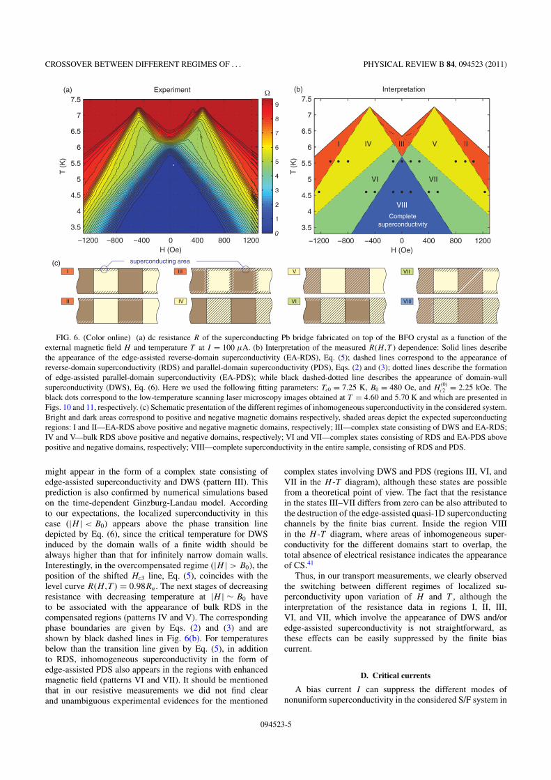
CROSSOVER BETWEEN DIFFERENT REGIMES OF . . . PHYSICAL REVIEW B 84, 094523 (2011)
H (Oe)
T (
K)
(a) Experiment Ω
−1200 −800 −400 0 400 800 1200
3.5
4
4.5
5
5.5
6
6.5
7
7.5
0
1
2
3
4
5
6
7
8
9
−1200 −800 −400 0 400 800 1200
3.5
4
4.5
5
5.5
6
6.5
7
7.5
Completesuperconductivity
I IV III V II
VI VII
VIII
H (Oe)
T (
K)
(b) Interpretation
I
II
V
VI
(c)VII
VIII
III
IV
superconducting area
FIG. 6. (Color online) (a) dc resistance R of the superconducting Pb bridge fabricated on top of the BFO crystal as a function of theexternal magnetic field H and temperature T at I = 100 μA. (b) Interpretation of the measured R(H,T ) dependence: Solid lines describethe appearance of the edge-assisted reverse-domain superconductivity (EA-RDS), Eq. (5); dashed lines correspond to the appearance ofreverse-domain superconductivity (RDS) and parallel-domain superconductivity (PDS), Eqs. (2) and (3); dotted lines describe the formationof edge-assisted parallel-domain superconductivity (EA-PDS); while black dashed-dotted line describes the appearance of domain-wallsuperconductivity (DWS), Eq. (6). Here we used the following fitting parameters: Tc0 = 7.25 K, B0 = 480 Oe, and H
(0)c2 = 2.25 kOe. The
black dots correspond to the low-temperature scanning laser microscopy images obtained at T = 4.60 and 5.70 K and which are presented inFigs. 10 and 11, respectively. (c) Schematic presentation of the different regimes of inhomogeneous superconductivity in the considered system.Bright and dark areas correspond to positive and negative magnetic domains respectively, shaded areas depict the expected superconductingregions: I and II—EA-RDS above positive and negative magnetic domains, respectively; III—complex state consisting of DWS and EA-RDS;IV and V—bulk RDS above positive and negative domains, respectively; VI and VII—complex states consisting of RDS and EA-PDS abovepositive and negative domains, respectively; VIII—complete superconductivity in the entire sample, consisting of RDS and PDS.
might appear in the form of a complex state consisting ofedge-assisted superconductivity and DWS (pattern III). Thisprediction is also confirmed by numerical simulations basedon the time-dependent Ginzburg-Landau model. Accordingto our expectations, the localized superconductivity in thiscase (|H | < B0) appears above the phase transition linedepicted by Eq. (6), since the critical temperature for DWSinduced by the domain walls of a finite width should bealways higher than that for infinitely narrow domain walls.Interestingly, in the overcompensated regime (|H | > B0), theposition of the shifted Hc3 line, Eq. (5), coincides with thelevel curve R(H,T ) = 0.98Rn. The next stages of decreasingresistance with decreasing temperature at |H | ∼ B0 haveto be associated with the appearance of bulk RDS in thecompensated regions (patterns IV and V). The correspondingphase boundaries are given by Eqs. (2) and (3) and areshown by black dashed lines in Fig. 6(b). For temperaturesbelow than the transition line given by Eq. (5), in additionto RDS, inhomogeneous superconductivity in the form ofedge-assisted PDS also appears in the regions with enhancedmagnetic field (patterns VI and VII). It should be mentionedthat in our resistive measurements we did not find clearand unambiguous experimental evidences for the mentioned
complex states involving DWS and PDS (regions III, VI, andVII in the H -T diagram), although these states are possiblefrom a theoretical point of view. The fact that the resistancein the states III–VII differs from zero can be also attributed tothe destruction of the edge-assisted quasi-1D superconductingchannels by the finite bias current. Inside the region VIIIin the H -T diagram, where areas of inhomogeneous super-conductivity for the different domains start to overlap, thetotal absence of electrical resistance indicates the appearanceof CS.41
Thus, in our transport measurements, we clearly observedthe switching between different regimes of localized su-perconductivity upon variation of H and T , although theinterpretation of the resistance data in regions I, II, III,VI, and VII, which involve the appearance of DWS and/oredge-assisted superconductivity is not straightforward, asthese effects can be easily suppressed by the finite biascurrent.
D. Critical currents
A bias current I can suppress the different modes ofnonuniform superconductivity in the considered S/F system in
094523-5

A. YU. ALADYSHKIN et al. PHYSICAL REVIEW B 84, 094523 (2011)
−1000 −500 0 500 1000−12
−8
−4
0
4
8
12(a) T = 3.50 K
H (Oe)
I (m
A)
−1000 −500 0 500 1000−12
−8
−4
0
4
8
12(b) T = 4.50 K
H (Oe)−1000 −500 0 500 1000
−12
−8
−4
0
4
8
12(c) T=5.50 K
H (Oe)−1000 −500 0 500 1000
−12
−8
−4
0
4
8
12(d) T = 6.50 K
H (Oe)
FIG. 7. (Color online) dc resistance R = V/I dependence of the long superconducting Pb bridge on the external magnetic field H and thebias current I taken at different temperatures: T = 3.50 K (a), T = 4.50 K (b), T = 5.50 K (c), and T = 6.50 K (d). We use the same colorscheme as in Fig. 6(a).
various ways. The effect of H and I on the current (I )-voltage(V ) dependencies and on the dc resistance R = V/I areillustrated in Figs. 7 and 8. We observed that the state ofRDS is more robust with respect to current injection than thestate of CS, since in the latter case the bias current can firstdestroy the weakly developed superconductivity above parallelmagnetic domains (i.e., above positive domains at H > 0 andvice versa), where the local magnetic field is maximal.
In order to evaluate the critical current destroying CS andRDS, we consider the effect of T on the I -V dependencies(Fig. 8) measured at H = 0 and |H | B0 (i.e., close to thecompensation field). One can see that the state with zeroresistance, which is inherent to CS, can be destroyed if I
exceeds a threshold value ICSc . Taking the position of the
jumps in the I -V curves at H = 0 or the maximal differentialresistance dR/dH [Fig. 8(a)], we plotted the the temperaturedependence of the critical current ICS
c , corresponding to thedestruction of the most developed CS state at H = 0. Fora characterization of the critical current IRDS
c , correspondingto the suppression of the developed RDS at the compensationfield (|H | B0), we traced the position of the jump on the I -Vcurves at H = 480 Oe upon increasing T [Fig. 8(a)]. Indeed,this estimate seems to be reasonable for the describing of thecurrent-induced destruction of inhomogeneous superconduc-tivity under the condition when the minimal resistance of theinvestigated sample in the superconducting state is finite (ofthe order of 50%Rn). The dependencies of the both estimatedcritical currents IRDS
c and IRDSc as a function of T are presented
in Fig. 9.
IV. VISUALIZATION OF NONUNIFORMSUPERCONDUCTING STATES BY SCANNING
LASER MICROSCOPY
In order to image the inhomogeneous superconductingstates trapped by the nonuniform magnetic field, we usedlow-temperature scanning laser microscopy (LTSLM).
The principle of operation of LTSLM can be introduced asfollows.9,42–45 The hybrid S/F samples were mounted on thecold finger of a helium gas flow cryostat, which is equippedwith optical windows to enable laser irradiation. An amplitudemodulated laser beam (wavelength 680 nm, modulationfrequency 10 kHz) heats locally the superconducting sample
within a spot with a diameter of 1.5–2 μm. This value isdetermined by the diameter of the focused incident beam andby the thermal conductivity of the tested bilayer sample.43
The incident beam intensity power on the sample surface(up to ∼25 μW) appears to be high enough to provide a maxi-mum beam-induced increase in temperature T ∼ 0.1–0.2 K,leading to a local suppression of superconductivity within this
−10 −8 −6 −4 −2 0 2 4 6 8 10−100
−50
0
50
100
3.50
K
4.00
K
4.50
K
5.00
K
5.50
K
7.00
K
I (mA)
V (
mV
)
(a)H = 0
V=IRn /2
V=IRn
−10 −8 −6 −4 −2 0 2 4 6 8 10−100
−50
0
50
100
4.00
K
4.50
K
5.00
K
5.50
K
6.00
K
6.50
K
7.00
K
I (mA)
V (
mV
)
(b)H = 480 Oe
V=IRn /2
V=IRn
FIG. 8. (Color online) Typical I -V dependencies measured atH = 0 (a) and H = 480 Oe (b) for the long superconducting Pbbridge at different temperatures indicated in the plots. Two dashedlines correspond to the Ohmic-like behavior with the resistance R =Rn/2 and R = Rn.
094523-6

CROSSOVER BETWEEN DIFFERENT REGIMES OF . . . PHYSICAL REVIEW B 84, 094523 (2011)
3 4 5 6 70
2
4
6
8Long bridge (I<0)Long bridge (I>0)Short bridge (I<0)Short bridge (I>0)
0.00
1.66
5.00
6.66
I c (m
A)
j c (10
5 A/c
m2 )
T (K)
T*
Reverse−domainsuperconductivity
Ic RDS
Completesuperconductivity
Ic CS
FIG. 9. (Color online) Temperature dependence of the criticalcurrents IRDS
c and ICSc , corresponding to the suppression of reverse-
domain superconductivity (red/light gray symbols near the top line),and complete superconductivity (blue/gray squares near the bottomline), respectively. For the determination of IRDS
c (ICS) we plottedthe positions of the maximal differential resistance on the I -Vdependencies measured at H = 480 Oe (H = 0) both for the longand short bridges; I < 0 and I > 0 denote the negative and positivebranches of the corresponding I -V curves (Fig. 8). The dashed linesare guides to the eyes.
hot spot. We assume that the effect of the laser irradiationshould be uniform across the superconducting film thicknesssince the thickness of the Pb film (40 nm) is much smaller than
the lateral spot size. In our LTSLM measurements we apply aconstant bias current and measure the beam-induced voltagedrop V along the entire bridge by lock-in technique. A setof scanning mirrors allows us to control the position (x,y) ofthe spot and thus to obtain the position-dependent 2D map ofthe LTSLM signal: V = V (x,y).
The LTSLM voltage signal can be interpreted as follows.If the laser spot heats an area of the bridge which is in thenormal resistive state, the beam-induced perturbation of thelocal temperature causes only a very small change in the totalresistance, since ∂Rn/∂T is very small. However, if the irradi-ated part of the bridge is in the superconducting state and it tookpart in the transfer of a substantial part of the supercurrents, thebeam-induced suppression of superconductivity might switchthe whole sample from a low-resistive state to a high-resistivestate. In other words, the LTSLM technique makes it possibleto map out the ability of the sample to carry supercurrents.Comparing the LTSLM responses upon varying H and T , onecan trace the evolution of local superconducting properties inthe investigated system.
For the observation of the different regimes of inhomoge-neous superconductivity in the long Pb/BFO hybrid samples,we applied a constant current of I = 300 μA and the field wasvaried in the range between H = ±1350 Oe.
Figure 10 shows the LTSLM images obtained at T =4.60 K, which is below the crossover temperature T ∗ =5.70 K (see Fig. 11). For |H | 130 Oe the measuredresponses have no detectable variations [see Figs. 10(a),10(b1), and 10(b2)]. Apparently, at these points inside the
LTSLM images at T = 4.60 K
ΔV (μV)
(a)
H=0 Oe
(b1)
(c1)
(d1)
(e1)
(f1)
(b2)
(c2)
(d2)
(e2)
(f2)
−130 Oe
−400 Oe
−530 Oe
−1230 Oe
−1350 Oe
+130 Oe
+400 Oe
+530 Oe
+1230 Oe
+1350 Oe
0
1
2
3
4
5
6
7
8
FIG. 10. (Color online) Low-temperature scanning laser microscopy (LTSLM) images obtained for the same area of the long Pb bridgeat T = 4.60 K. The color scale indicates the change in the beam-induced voltage drop V . The H values are indicated in the plots and thebias points for all presented images are also marked by black dots in the phase diagram in Fig. 6(b). The scanning area is ∼120 μm × 40 μm.Vertical dashed cyan (light gray) lines indicate the positions of the domain walls. The sample edges are marked by horizontal solid whitelines.
094523-7

A. YU. ALADYSHKIN et al. PHYSICAL REVIEW B 84, 094523 (2011)
LTSLM images at T = 5.50 K
ΔV (μV)
(a)
H=0 Oe
(b1)
(c1)
(d1)
(e1)
(f1)
(b2)
(c2)
(d2)
(e2)
(f2)
−130 Oe
−800 Oe
−940 Oe
−1060 Oe
+130 Oe
+260 Oe
+800 Oe
+940 Oe
+1060 Oe
0
1
2
3
4
5
6
7
8
FIG. 11. (Color online) Low-temperature scanning laser microscopy (LTSLM) images obtained for the same area of the long Pb bridge atT = 5.50 K. All parameters and notations are the same as in Fig. 10. The LTSLM image at H = −260 Oe (c1) was recorded with technicalproblems and therefore we do not present this plot.
CS state in the H -T diagram, the intensity of the laserbeam is insufficient for the destruction of the developed bulksuperconductivity.
According to our estimates, at T = 4.60 K, the depletion ofsuperconductivity above the parallel magnetic domains shouldoccur at |H | 350 Oe. This means that near the “CS-RDS”transition line the areas above the parallel domains have tobe in the resistive state, while the areas above the oppositedomains are still in the superconducting state. As a result,the maxima in the LTSLM response at H = 400 Oe should beattributed solely to the nonsuperconducting regions above thepositive domains [Figs. 10(c2) and 10(d2)]. Correspondingly,at H = −400 Oe the resistive areas above negative domainsare responsible for the beam-induced voltage [Figs. 10(c1) and10(d1)]. At higher H values (i.e., deeper in the RDS areas in theH -T diagram) superconductivity survives exclusively abovethe opposite domains and such compensated superconductivityis strong enough not to be destroyed by the laser beam of thegiven intensity. However, close to the transition line “RDS–edge-assisted RDS,” describing the destruction of the bulkRDS, the bulk reverse-domain superconductivity becomesweaker and can be affected by the laser beam. Therefore,the bright areas in the corresponding LTSLM signal originatefrom the regions with the compensated magnetic field abovethe opposite domains. The inversion of the H sign immediatelyresults in a switching between enhanced reverse-domain super-conductivity and depleted parallel-domain superconductivityfor the same areas of the superconducting bridge [Figs. 10(e1)and 10(e2) and Figs. 10(f1) and 10(f2)]. Thus, all findingsconcerning the migration of the maximal beam-induced
voltage along the Pb bridge upon varying H are in agreementwith our transport measurements.
We would like to note that the LTSLM images[Figs. 10(c1)–10(f1) and 10(c2)–10(f2)] reveal an inhomo-geneity of the beam-induced voltage across the width of thebridge. Indeed, the V maxima are always located near theedges of the bridge. At the present moment we have no reliableinterpretation of this effect. Probably, it can be explained bythe current enhancement near the sample edges, typical forplain superconducting bridges,46,47 or by a suppression ofthe energy barrier for flux entry or exit for superconductorsin the developed mixed state. Another possible explanationfor the pronounced edge signal is the manifestation of edge-assisted PDS, since such edge-assisted PDS states seem to bethe states with weakest superconductivity. Finally, the edgesignal can be explained by a hampered heat diffusion and,correspondingly, a larger heating effect of the beam focusednear the edges as compared to that in the interior of the bridge.Thus, at the current state of our LTSLM measurements wecannot unambiguously interpret the inhomogeneous LTSLMsignal across the bridge as a clear evidence of the edge-assisted superconducting states. This issue requires a detailedtheoretical treatment which is beyond the scope of the presentwork.
At T = 5.50 K, close to the crossover temperature, avoltage signal can be detected at H = 0. The amplitude ofthe built-in magnetic field is close to the corresponding uppercritical field and therefore even a weak optical influence cansubstantially suppress bulk superconductivity equally abovethe domains of both polarities. Upon increasing |H | we
094523-8
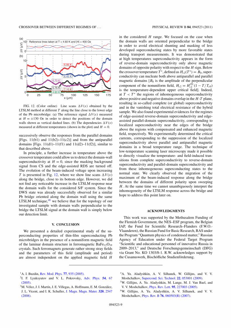
CROSSOVER BETWEEN DIFFERENT REGIMES OF . . . PHYSICAL REVIEW B 84, 094523 (2011)
0
10
0
5
10
Reference lines taken at T = 4.60 K and |H| = 400 Oe
0 25 50 75 100 125 150 1754.60 K
5.75 K
5.95 K
6.45 K
6.70 K
7.10 K
x (μm)
(b)
(a)
ΔV (
μV)
ΔV (
μV)
FIG. 12. (Color online) Line scans V (x) obtained by theLTSLM method at different T along the line close to the lower edgeof the Pb microbridge: (a) The reference signal V (x) measuredat H = ±130 Oe in order to detect the positions of the domainwalls shown as vertical dashed lines. (b) The dependencies V (x)measured at different temperatures (shown in the plot) and H = 0.
successively observe the responses from the parallel domains[Figs. 11(b1) and 11(b2)–11(c2)] and from the antiparalleldomains [Figs. 11(d1)–11(f1) and 11(d2)–11(f2)], similar tothat described above.
In principle, a further increase in temperature above thecrossover temperature could allow us to detect the domain-wallsuperconductivity at H = 0, since the masking backgroundsignal from CS and the edge-assisted RDS are turned off.The evolution of the beam-induced voltage upon increasingT is presented in Fig. 12, where we show line scans V (x)along the bridge, close to its bottom edge. However, we didnot find any noticeable increase in the LTSLM response nearthe domain walls for the considered S/F system. Since theDWS state was already successfully observed for a similarPb bridge oriented along the domain wall using the sameLTSLM technique,48 we believe that for the topology of ourinvestigated sample with domain walls perpendicular to thebridge the LTSLM signal at the domain wall is simply belowour detection limit.
V. CONCLUSION
We presented a detailed experimental study of the su-perconducting properties of thin-film superconducting Pbmicrobridges in the presence of a nonuniform magnetic fieldof the laminar domain structure in ferromagnetic BaFe12O19
crystals. Such ferromagnets generate rather strong stray fieldsand the parameters of this field (amplitude and period)are almost independent on the applied magnetic field H
in the considered H range. We focused on the case whenthe domain walls are oriented perpendicular to the bridgein order to avoid electrical shunting and masking of lessdeveloped superconducting states by more favorable statesduring transport measurements. It was demonstrated thatat high temperatures superconductivity appears in the formof reverse-domain superconductivity only above magneticdomains of opposite polarity with respect to the H sign. Belowthe crossover temperature T ∗, defined as Hc2(T ∗) = B0, super-conductivity can nucleate both above antiparallel and parallelmagnetic domains [B0 is the amplitude of the perpendicularcomponent of the nonuniform field, Hc2 = H
(0)c2 (1 − T/Tc0)
is the temperature-dependent upper critical field]. Indeed,at T < T ∗ the regions of inhomogeneous superconductivityabove positive and negative domains overlap in the H -T plane,resulting in so-called complete (or global) superconductivityand in the vanishing total electrical resistance of the hybridsample. We also found experimental evidences for the regimesof edge-assisted reverse-domain superconductivity and edge-assisted parallel-domain superconductivity, corresponding tolocalized superconductivity near the edges of the bridgeabove the regions with compensated and enhanced magneticfield, respectively. We experimentally determined the criticalcurrents, corresponding to the suppression of the localizedsuperconductivity above parallel and antiparallel magneticdomains in a broad temperature range. The technique oflow-temperature scanning laser microscopy made it possibleto directly visualize the temperature- and field-induced tran-sitions from complete superconductivity to reverse-domainsuperconductivity and parallel-domain superconductivity andfrom these inhomogeneous superconducting states to thenormal state. We clearly observed the migration of themaximum of the beam-induced response along the bridgebetween the domains of different polarity upon sweepingH . At the same time we cannot unambiguously interpret theinhomogeneity of the LTSLM response across the bridge andhope to address this point later on.
ACKNOWLEDGMENTS
This work was supported by the Methusalem Funding ofthe Flemish Government, the NES–ESF program, the BelgianIAP, the Fund for Scientific Research–Flanders (F.W.O.-Vlaanderen), the Russian Fund for Basic Research, RAS underthe Program “Quantum physics of condensed matter,” RussianAgency of Education under the Federal Target Program“Scientific and educational personnel of innovative Russia in2009–2013,” and Deutsche Forschungsgemeinschaft (DFG)via Grant No. KO 1303/8-1. R.W. acknowledges support bythe Cusanuswerk, Bischofliche Studienforderung.
1A. I. Buzdin, Rev. Mod. Phys. 77, 935 (2005).2I. F. Lyuksyutov and V. L. Pokrovsky, Adv. Phys. 54, 67(2005).
3M. Velez, J. I. Martın, J. E. Villegas, A. Hoffmann, E. M. Gonzalez,J. L. Vicent, and I. K. Schuller, J. Magn. Magn. Mater. 320, 2547(2008).
4A. Yu. Aladyshkin, A. V. Silhanek, W. Gillijns, and V. V.Moshchalkov, Supercond. Sci. Technol. 22, 053001 (2009).
5W. Gillijns, A. Yu. Aladyshkin, M. Lange, M. J. Van Bael, andV. V. Moshchalkov, Phys. Rev. Lett. 95, 227003 (2005).
6W. Gillijns, A. Yu. Aladyshkin, A. V. Silhanek, and V. V.Moshchalkov, Phys. Rev. B 76, 060503(R) (2007).
094523-9

A. YU. ALADYSHKIN et al. PHYSICAL REVIEW B 84, 094523 (2011)
7A. Yu. Aladyshkin, A. P. Volodin, V. V. Moshchalkov, J. Appl. Phys.108, 033911 (2010).
8Z. Yang, M. Lange, A. Volodin, R. Szymczak, and V. V.Moshchalkov, Nat. Mater. 3, 793 (2004).
9J. Fritzsche, V. V. Moshchalkov, H. Eitel, D. Koelle, R. Kleiner,and R. Szymczak, Phys. Rev. Lett. 96, 247003 (2006).
10Z. Yang, J. van de Vondel, W. Gillijns, W. Vinckx, V. V.Moshchalkov, and R. Szymczak, Appl. Phys. Lett. 88, 232505(2006).
11Z. Yang, K. Vervaeke, V. V. Moshchalkov, and R. Szymczak, Phys.Rev. B 73, 224509 (2006).
12A. Yu. Aladyshkin, J. Fritzsche, and V. V. Moshchalkov, Appl.Phys. Lett. 94, 222503 (2009).
13A. Yu. Aladyshkin, J. Fritzsche, and V. V. Moshchalkov, Physica C470, 883 (2010).
14A. Yu. Aladyshkin, D. Yu. Vodolazov, J. Fritzsche, R. B. G.Kramer, and V. V. Moshchalkov, Appl. Phys. Lett. 97, 052501(2010).
15L. Y. Zhu, T. Y. Chen, and C. L. Chien, Phys. Rev. Lett. 101, 017004(2008).
16L. Y. Zhu, Marta Z. Cieplak, and C. L. Chien, Phys. Rev. B 82,060503(R) (2010).
17S. Haindl, M. Weisheit, T. Thersleff, L. Schultz, and B. Holzapfel,Supercond. Sci. Technol. 21, 045017 (2008).
18J. Fritzsche, R. B. G. Kramer, and V. V. Moshchalkov, Phys. Rev.B 80, 094514 (2009).
19V. K. Vlasko-Vlasov, U. Welp, A. Imre, D. Rosenmann, J. Pearson,and W. K. Kwok, Phys. Rev. B 78, 214511 (2008).
20V. Vlasko-Vlasov, U. Welp, G. Karapetrov, V. Novosad,D. Rosenmann, M. Iavarone, A. Belkin, and W.-K. Kwok, Phys.Rev. B 77, 134518 (2008).
21V. Vlasko-Vlasov, U. Welp, W. Kwok, D. Rosenmann, H. Claus,A. A. Buzdin, and A. Melnikov, Phys. Rev. B 82, 100502(R)(2010).
22C. Bell, S. Tursucu, and J. Aarts, Phys. Rev. B 74, 214520 (2006).23R. K. Rakshit, R. C. Budhani, T. Bhuvana, V. N. Kulkarni, and
G. U. Kulkarni, Phys. Rev. B 77, 052509 (2008).24R. K. Rakshit, S. K. Bose, R. Sharma, N. K. Pandey, and R. C.
Budhani, Phys. Rev. B 77, 094505 (2008).25A. Belkin, V. Novosad, M. Iavarone, J. Fedor, J. E. Pearson,
A. Petrean-Troncalli, and G. Karapetrov, Appl. Phys. Lett. 93,072510 (2008).
26A. Belkin, V. Novosad, M. Iavarone, J. Pearson, and G. Karapetrov,Phys. Rev. B 77, 180506 (2008).
27G. Karapetrov, M. V. Milosevic, M. Iavarone, J. Fedor, A.Belkin, V. Novosad, and F. M. Peeters, Phys. Rev. B 80, 180506(2009).
28A. Belkin, V. Novosad, M. Iavarone, R. Divan, J. Hiller, T. Proslier,J. E. Pearson, and G. Karapetrov, Appl. Phys. Lett. 96, 092513(2010).
29C. Visani, N. M. Nemes, M. Rocci, Z. Sefrioui, C. Leon, S. G. E.te Velthuis, A. Hoffmann, M. R. Fitzsimmons, F. Simon, T. Feher,M. Garcia-Hernandez, and J. Santamaria, Phys. Rev. B 81, 094512(2010).
30T. Tamegai, Y. Nakao, S. Mohan, and Y. Nakajima, Supercond. Sci.Technol. 24, 024015 (2011).
31B. Pannetier, S. Rodts, J. L. Genicon, Y. Otani, and J. P.Nozieres, in Macroscopic Quantum Phenomena and Coherencein Superconducting Networks, edited by C. Giovannella andM. Tinkham (World Scientific, Singapore, 1995 ), pp. 17–24.
32M. Lange, M. J. Van Bael, Y. Bruynseraede, and V. V. Moshchalkov,Phys. Rev. Lett. 90, 197006 (2003).
33A. Yu. Aladyshkin, A. I. Buzdin, A. A. Fraerman, A. S. Mel’nikov,D. A. Ryzhov, and A. V. Sokolov, Phys. Rev. B 68, 184508(2003).
34M. V. Milosevic, G. R. Berdiyorov, and F. M. Peeters, Phys. Rev.Lett. 95, 147004 (2005).
35A. Yu. Aladyshkin and V. V. Moshchalkov, Phys. Rev. B 74, 064503(2006).
36A. I. Buzdin and A. S. Mel’nikov, Phys. Rev. B 67, 020503(R)(2003).
37D. Saint-James, G. Sarma, and E. J. Thomas, Type II Superconduc-tivity (Pergamon, Oxford, UK, 1969).
38M. Tinkham, Introduction to Superconductivity, 2nd ed. (McGraw-Hill, New York, 1996).
39Equation (6) may be considered as an ultimate estimate of DWS,since the critical temperature of the solution, localized in vicinityof the domain walls of the finite width, will be always higher thanthat given by Eq. (6).
40S. J. Bending, Adv. Phys. 48, 449 (1999).41Since these tested S/F samples were degraded after the experimental
LTSLM session, we were unable to complete our study by anotherseries of transport measurements and/or LTSLM images for thesame samples, i.e., in order to show the effect of the bias current onthe measured characteristics.
42L. R. Testardi, Phys. Rev. B 4, 2189 (1971).43J. Fritzsche, Ph.D. thesis, Katholieke Universiteit Leuven, 2008.44M. Wagenknecht, H. Eitel, T. Nachtrab, J. B. Philipp,
R. Gross, R. Kleiner, and D. Koelle, Phys. Rev. Lett. 96, 047203(2006).
45H. B. Wang, S. Guenon, J. Yuan, A. Iishi, S. Arisawa, T. Hatano,T. Yamashita, D. Koelle, and R. Kleiner, Phys. Rev. Lett. 102,017006 (2009).
46M. Yu. Kupriyanov and K. K. Likharev, Fiz. Tverd. Tela 16, 2829(1974) [Sov. Phys. Solid State 16, 1835 (1975)].
47A. A. Elistratov, D. Yu. Vodolazov, I. L. Maksimov, and J. R. Clem,Phys. Rev. B 66, 220506 (2002).
48R. Werner, A. Yu. Aladyshkin, S. Guenon, J. Fritzsche, I. M.Nefedov, V. V. Moshchalkov, R. Kleiner, and D. Koelle, Phys.Rev. B 84, 020505(R) (2011).
094523-10

Publication II


RAPID COMMUNICATIONS
PHYSICAL REVIEW B 84, 020505(R) (2011)
Domain-wall and reverse-domain superconducting states of a Pb thin-film bridgeon a ferromagnetic BaFe12O19 single crystal
R. Werner,1 A. Yu. Aladyshkin,2,3 S. Guenon,1 J. Fritzsche,2 I. M. Nefedov,3 V. V. Moshchalkov,2 R. Kleiner,1 and D. Koelle1,*
1Physikalisches Institut–Experimentalphysik II and Center for Collective Quantum Phenomena in LISA+, Universitat Tubingen,Auf der Morgenstelle 14, D-72076 Tubingen, Germany
2INPAC–Institute for Nanoscale Physics and Chemistry, K.U. Leuven, Celestijnenlaan 200D, B-3001 Leuven, Belgium3Institute for Physics of Microstructures RAS, 603950 Nizhny Novgorod, GSP-105, Russia
(Received 14 February 2011; revised manuscript received 13 May 2011; published 20 July 2011)
We report on imaging of the nonuniform superconducting states in a Pb thin-film bridge on top of aferromagnetic BaFe12O19 single crystal with a single straight domain wall along the center of the bridge bylow-temperature scanning laser microscopy. We have visualized domain-wall superconductivity (DWS) close tothe critical temperature of Pb, when the Pb film above the domain wall acts as a superconducting path for thecurrent. The evolution of the DWS signal with temperature and the external-field-driven transition from DWS toreverse-domain superconductivity was visualized.
DOI: 10.1103/PhysRevB.84.020505 PACS number(s): 74.78.Na, 74.25.Op, 75.47.−m
It is well known that so-called surface or bound states canbe generated by the presence of boundaries in a material.For example, the formation of surface states for a singleelectron wave function in a semi-infinite crystalline latticedue to the modification of the boundary conditions wasdescribed by Tamm1 and by Shockley.2 Other examples ofbound states are surface plasmons, propagating along theinterface between a dielectric and a metal,3–5 and surfaceacoustic waves traveling along the surface of a materialexhibiting elasticity.6,7 In both latter cases these waves areconfined in the direction perpendicular to the wave vector,i.e., their amplitudes decay exponentially far from the inter-face or surface. The formation of surface bound states forthe superconducting order-parameter wave function wasconsidered by Saint-James and de Gennes.8,9 They showed thatlocalized superconductivity at a superconductor (S)/vacuumor S/insulator interface can appear at an applied magneticfield Hext above the upper critical field Hc2 for bulk supercon-ductivity. Similarly to this surface superconductivity, localizedsuperconductivity can also nucleate near the sample edge ina thin semi-infinite superconducting film10 or in a thin super-conducting disk of very large diameter11 in a perpendicularmagnetic field. Such so-called edge superconductivity (ES),with transition temperature T ES
c , has the same phase-transitionline as surface superconductivity,12 given by 1 − T ES
c /Tc0 0.59 |Hext|/H (0)
c2 . Here, Tc0 is the superconducting transitiontemperature in zero magnetic field, H
(0)c2 = 0/(2πξ 2
0 ) and ξ0
are the upper critical field and coherence length at temperatureT = 0, respectively, and 0 = πhc/e is the magnetic-fluxquantum. This means that ES will survive up to the criticalfield Hc3 = 1.69Hc2, while above Hc2 = H
(0)c2 (1 − T/Tc0)
bulk superconductivity is totally suppressed.An alternative way to prepare localized states in supercon-
ducting films is to confine the order-parameter wave functionby a nonuniform magnetic field in hybrid S/ferromagnet(F ) structures (see, e.g., Ref. 13 and references therein).Buzdin and Mel’nikov14 considered a steplike distributionbz(x) = B0 sgn(x) of the perpendicular component of themagnetic field, Bz = Hext + bz, induced by domain wallsin the ferromagnet (with the z axis perpendicular to the
film surface). They demonstrated that superconductivity willsurvive in vicinity along the step, even if the amplitude ofthe nonuniform magnetic B0 > Hc2. The dependence of thetransition temperature T DWS
c (Hext) for domain-wall supercon-ductivity (DWS) in a plain superconducting film (i.e., infinitein lateral direction) can be estimated as 1 − T DWS
c /Tc0 0.59 − 0.70(Hext/B0)2 + 0.09(Hext/B0)4B0/H
(0)c2 .15
For flux-coupled S/F structures of finite lateral size thelocalized states of ES and DWS may compete as illustrated inFig. 1 for the case of a thin-film S strip of finite width above a F
substrate with a domain wall along the center of the bridge, forHc2 < B0 < Hc3. For a domain structure with steplike bz(x)profile and Hext = 0, ES and DWS nucleate simultaneouslyin the S strip as shown in Fig. 1(a). Figure 1(b) shows thecase of a domain wall with finite width and Hext = 0. Here,DWS becomes energetically more favorable compared to ESand only DWS nucleates.16 For Hext = 0, the local field iscompensated above the domain with magnetization directionopposite to Hext. If ||Hext| − B0| < Hc2 superconductivity isturned on above this reverse domain while it is still suppressedabove the parallel domain [cf. Fig. 1(c)]. This effect is termedreverse-domain superconductivity (RDS).17,18 We note thatwhen Hc2 becomes larger than |Hext| + B0 (e.g., upon cooling)above the parallel domain, superconductivity may also nucle-ate there and the entire strip will be in the superconductingstate, which we call complete superconductivity (CS).
Fingerprints of RDS and DWS have been found byelectric transport measurements on S/F hybrids with a rathercomplex domain structure in BaFe12O19 (BFO) crystals17
and multilayered CoPt films19 with perpendicular magneticanisotropy. Using low-temperature scanning laser microscopy(LTSLM), RDS has been visualized in a hybrid Nb/PbFe12O19
system.18 However, due to the complex domain structureand relatively small domain size, visualization of DWS wasnot possible. Recently, significant improvements have beenachieved, regarding the fabrication of specially polishedBFO crystals, characterized by a well defined and stabledomain structure with straight domain walls separated bytypically 30 μm.20,21 Here we report on the direct imagingof the development of DWS and RDS in a hybrid S/F
020505-11098-0121/2011/84(2)/020505(4) ©2011 American Physical Society

RAPID COMMUNICATIONS
R. WERNER et al. PHYSICAL REVIEW B 84, 020505(R) (2011)
DWS(b)DWS
M
0
-Hc2
ES
M
(a)
-Hc3
B0
x
bz
| |Ψ
x
| |Ψ
bz
M
RDS
M
Hext
b +Hz ext
| |Ψ
bz
M
Hc3
Hc2
(c)
x
0
FIG. 1. (Color online) Illustration of DWS, ES, and RDS acrossa thin-film S strip on top of a F substrate with two domains withperpendicular magnetization M. Magnetic-field profiles Bz(x) =Hext + bz(x) inside the S strip generated by the domains underneathand modulus of superconducting order parameter |(x)| are shownfor (a) steplike bz(x) for Hext = 0, (b) field profile with finite widthfor Hext = 0, and (c) finite Hext ≈ B0. White dashed lines indicateupper critical fields ±Hc2 and ±Hc3.
structure, consisting of a superconducting Pb film on top of aferromagnetic BFO crystal by means of LTSLM.18,22–25
We prepared a 40-nm-thick and 30-μm-wide Pb micro-bridge on top of a BFO substrate, so that only a single domainwall is running along the center of the Pb bridge parallel to thecurrent flow. The BFO substrate and the Pb thin film were sep-arated by a 4-nm-thick insulating Ge layer so that the systemis only flux coupled. From resistance R vs Hext measurementsat variable T of a reference sample with several domain wallsoriented perpendicular to the long side of the bridge,26 wecompose the Hext-T phase diagram shown in Fig. 2(b).
For imaging by LTSLM, the sample was mounted on thecold finger of a helium gas flow cryostat, with an opticalwindow to enable irradiation of the sample surface in the(x,y) plane by a focused laser beam with beam spot diameter∼1.5–2 μm.24,25 The amplitude modulated laser beam (at fre-quency f ≈ 10 kHz) induces a local increase of temperatureδT (x − x0,y − y0) centered at the beam spot position (x0,y0)on the sample surface. During imaging, the Pb bridge is biasedat a constant current I , and the beam-induced change ofvoltage V (x0,y0) is recorded with lock-in technique. TheLTSLM voltage signal can be interpreted as follows: If theirradiated part of the sample was in the normal state withresistivity ρn, the laser beam induces a very small voltagesignal V ∝ ∂ρn/∂T . However, if the irradiated region tookpart in the transfer of a substantial part of the supercurrents, thebeam-induced suppression of superconductivity might switchthe sample from a low-resistive state to a high-resistive state.This effect should be maximal if I is close to the overallcritical current Ic = Ic(T ,Hext) of the sample. In this caseLTSLM allows one to map out the ability of the sample tocarry supercurrents.
In order to trace out the evolution of DWS with temperature,we recorded a series of LTSLM voltage images V (x,y) atHext = 0 and different T across the resistive transition of thePb bridge. Figure 2(a) shows the R(T ) curve of the Pb/BFOmicrobridge; the labels 1–8 indicate the bias points for whichLTSLM images and line scans are shown in Figs. 2(d) and 2(c),respectively. The dots in the Hext-T phase diagram shown inFig. 2(b) indicate the bias points for which LTSLM data areshown. LTSLM voltage images 1–8 in Fig. 2(d) show theevolution of the superconducting properties of the Pb/BFObridge upon cooling through Tc (from left to right) at Hext = 0;
0.00.10.20.30.40.50.60.70.80.9ΔV (µV)(d) 0 60 x (µm)
optical image5.7 K6.4 K 6.3 K 6.2 K 6.1 K 6.0 K
)c()b()a(
6.6 K1 2 3 4 5 6 7 5.0 K8
FIG. 2. (Color) Evolution of DWS upon cooling through Tc and Hext-T phase diagram. (a) R(T ) curve (I = 100 μA); dots indicate biaspoints of LTSLM voltage images 1–8 in (d) and corresponding line scans in (c). (b) Hext-T phase diagram, constructed from experimentallydetermined values Tc0 = 7.25 K, B0 = 480 G, and H
(0)c2 = 2.25 kOe. The phase diagram contains separate regions of DWS, ES, RDS, and CS.
Dots label bias points for LTSLM data shown in (c), (d), and Fig. 3. (c) Line scans V (x) across the bridge for different T , taken from voltageimages in (d). Red dots show simulation results for T = 6.4 K. The position of the edges of the bridge is indicated by dashed gray lines. (d) Seriesof LTSLM voltage images V (x,y) (1–8 from left to right) taken at different T during cooling the Pb bridge through its resistive transition (I =10 μA). White dashed lines indicate the position of line scans in (c). The graph on the right shows a corresponding optical LTSLM image.
020505-2

RAPID COMMUNICATIONS
DOMAIN-WALL AND REVERSE-DOMAIN . . . PHYSICAL REVIEW B 84, 020505(R) (2011)
(b)
-165 Oe 165 Oe0 10 20 30 40 50 600.0
0.2
0.4
0.6
0.8
V (
V)
x (µm)
Hext (Oe)
0336699
132165
(a)
FIG. 3. (Color online) Switching from DWS to RDS: variableHext at T = 6.2 K. (a) Line scans V (x) along white dashed linein (b) for different Hext 0; dashed gray lines indicate edges of thebridge. (b) LTSLM images for maximal |Hext|.
according to Fig. 2(b), these should cover the transitions fromthe normal state to DWS and finally to CS. The graph on theright shows an optical LTSLM image, in order to indicate sizeand position of the bridge in the voltage images.27 For a morequantitative analysis, in Fig. 2(c) we show line scans V (x)across the bridge [along the white dashed lines in Fig. 2(d)].
Starting with the highest temperature T = 6.6 K, thevoltage image in Fig. 2(d) and the corresponding line scan(black line) in Fig. 2(c) shows no signal, as the bridge is inthe normal state. Lowering T to 6.4 K [entering the resistivetransition shown in Fig. 2(a)], the voltage image gives asmall homogeneous signal with a broad maximum centeredabove the bridge [red line in Fig. 2(c)]. For a (still) resistivePb bridge with homogeneous conductivity but finite ∂R/∂T ,this behavior can be simply explained by the finite width ofthe beam-induced δT (x,y) profile, i.e., its tails will induce avoltage signal, even if the beam spot is positioned outside thebridge. This is confirmed by numerical simulations [cf. red datapoints in Fig. 2(c)], which solve the heat diffusion equationfor an absorbed laser power of 25 μW, a beam spot diameterof 2 μm and thermal conductivity of the BFO substrate of0.8 W cm−1 K−1. These simulations yield a maximum increasein beam-induced temperature T = 0.14 K.
Upon further cooling (see voltage images and correspond-ing line scans for T = 6.3 K and T = 6.2 K), a clear LTSLMsignal develops, running along the domain wall [green andblue lines, respectively, in Fig. 2(c)]. This observation can beinterpreted as an evidence that a channel above the domainwall with higher conductivity than the regions above thedomains has formed, and therefore the current density j (x)has a maximum above the domain wall. We note that, althoughaccording to the Hext-T phase diagram the sample should be inthe the DWS state, the overall resistance of the bridge is closeto the full normal resistance. This is consistent with numericalsimulations based on the time-dependent Ginzburg-Landauequations, which indicate that for our experimental situationthe critical current density jc,DWS along the domain-wallchannel is too small, i.e., the bias current might be above thecritical current of this channel. This also explains why, upondecreasing T , the LTSLM signal at the domain wall increases,as jc,DWS increases, and the peak in V (x) becomes sharper(see below). We did not find a similar enhancement of theLTSLM voltage signal at the edges of the bridge, i.e., we donot find any signature of ES. We attribute this to the finite
width of the domain wall, which stabilizes DWS compared toES.
For T < 6.2 K the amplitude of the peak of the LTSLMresponse at the domain wall decreases as T decreases, and themaximum of the LTSLM signal shifts toward the edges of thebridge; see magenta and orange lines in Fig. 2(c) for T = 6.0 Kand T = 5.7 K, respectively, and the corresponding voltageimages in Fig. 2(d). We interpret this observation as thetransition from DWS to CS, which is consistent with the phasediagram shown in Fig. 2(b). At this transition, CS spreadingover the whole sample becomes favorable and the sample isturned into the mixed state. The onset of CS can explain theappearance of two pronounced maxima in V (x) at the sampleedges: In the mixed state the current distribution depends onthe edge energy barrier for vortex entry. Upon laser irradiation,the edge energy barrier is locally suppressed, which in turnopens a gate for vortex entry/exit. Hence one can expect thatirradiation at the edges of the bridge should strongly affectthe vortex pattern and the resulting current distribution. Incontrast, laser irradiation of the interior of the bridge does notchange the existing energy barrier, and the modification ofthe current pattern is probably less pronounced, and thereforethe beam-induced voltage change is much smaller. Finally,at T = 5.0 K the LTSLM signal is zero [cf. Fig. 2(d) andbrown line in Fig. 2(c)], which indicates that the bridge is inthe CS state and the beam-induced perturbation is not strongenough to suppress superconductivity and induce a voltagesignal.
Finally, we investigated the effect of finite perpendicularfield |Hext| 165 Oe on superconductivity in our system.The measurements were carried out at T = 6.2 K, whichcorresponds to the most pronounced LTSLM signal above thedomain wall at Hext = 0. Figure 3(a) shows the evolution ofthe LTSLM voltage signal V (x) with increasing externalfield for positive polarity. For Hext = 0 the DWS signal isclearly visible as described above. With increasing Hext theamplitude of the domain-wall signal decreases monotonouslywhile its width stays roughly constant. Simultaneously a signalabove the reverse (right) domain appears. In the RDS state, forHext 70 Oe, the voltage signal shows a peak at the rightedge of the bridge, which can be explained in the same wayas for the edge signal discussed in the context of the T seriesshown in Fig. 2. Figure 3(b) shows LTSLM voltage imagestaken at Hext = −165 Oe (left image) and Hext = +165 Oe(right image), which clearly demonstrate switching betweenthe RDS states above the two domains upon reversing thepolarity of the external field.
In conclusion, we have clearly identified the formationof the spatially inhomogeneous superconducting state in asuperconducting Pb thin film induced by the stray field ofthe domains in the ferromagnetic substrate BFO underneath.The crucial feature of the investigated system is that the su-perconducting Pb bridge was fabricated exactly above a singlestraight domain wall, which is running along the center of thebridge. Such a well-defined geometry of the hybrid Pb/BFOsample makes it possible to directly visualize the localized anddelocalized superconductivity by means of low-temperaturescanning laser microscopy. We imaged the evolution of DWSwith decreasing temperature. Using the external field as acontrol parameter, we demonstrated that superconductivity in
020505-3

RAPID COMMUNICATIONS
R. WERNER et al. PHYSICAL REVIEW B 84, 020505(R) (2011)
a wide superconducting bridge can be switched from the DWSto RDS state. This opens up interesting perspectives for the cre-ation of spatially nonuniform superconducting states and fortheir manipulation by external and “internal” magnetic fields.
This work was funded by DFG via Grant No. KO 1303/8-1,the Methusalem Funding of the Flemish Government, the
NES-ESF program, the Belgian IAP, the Fund for Sci-entific Research–Flanders (F.W.O.-Vlaanderen), the RFBR,RAS under the Program “Quantum physics of condensedmatter,” and FTP “Scientific and educational personnel ofinnovative Russia in 2009–2013.” R.W. gratefully acknowl-edges support by the Cusanuswerk, Bischofliche Studi-enforderung.
*[email protected]. Tamm, Phys. Z. Sowjetunion 1, 733 (1932).2W. Shockley, Phys. Rev. 56, 317 (1939).3R. H. Ritchie, Phys. Rev. 106, 874 (1957).4L. D. Landau and E. M. Lifshitz, Electrodynamics of ContinuousMedia, 2nd ed. (Pergamon, New York, 1984).
5S. A. Maier, Plasmonics: Fundamentals and Applications(Springer, New York, 2007).
6Lord Rayleigh, in Proc. London Math. Soc. 17, 4 (1885).7Acoustic Surface Waves, Topics in Applied Physics Vol. 24,edited by A. A. Oliner (Springer-Verlag, Berlin, 1978).
8D. Saint-James and P. G. de Gennes, Phys. Lett. 7, 306 (1963).9D. Saint-James, G. Sarma, and E. J. Thomas, Type II Superconduc-tivity (Pergamon, New York, 1969).
10R. H. White, Phys. Rev. 142, 241 (1966).11A. Y. Aladyshkin, D. A. Ryzhov, A. V. Samokhvalov, D. A. Savinov,
A. S. Melnikov, and V. V. Moshchalkov, Phys. Rev. B 75, 184519(2007).
12M. Tinkham, Introduction to Superconductivity, 2nd ed. (McGraw-Hill, New York, 1996).
13A. Y. Aladyshkin, A. V. Silhanek, W. Gillijns, and V. V.Moshchalkov, Supercond. Sci. Technol. 22, 053001 (2009).
14A. I. Buzdin and A. S. Mel’nikov, Phys. Rev. B 67, 020503(R)(2003).
15A. Y. Aladyshkin, A. I. Buzdin, A. A. Fraerman, A. S. Mel’nikov,D. A. Ryzhov, and A. V. Sokolov, Phys. Rev. B 68, 184508(2003).
16We calculate |(x)| by solving numerically the linearizedGinzburg-Landau equation for a thin superconducting bridge offinite width in the presence of the nonuniform field Bz(x) =Hext + (2B0/π ) arctan(x/L), following the approach of Ref. 15.The case L → 0 corresponds to a steplike field profile, and any
(even very small but) finite L gives a finite transient region forthe stray magnetic field near the domain wall. I.e., for the systeminvestigated here, with typical width 5–10 nm of the domain wallsin the BaFe12O19 substrate, ES will be suppressed.
17Z. R. Yang, M. Lange, A. Volodin, R. Szymczak, and V. V.Moshchalkov, Nat. Mater. 3, 793 (2004).
18J. Fritzsche, V. V. Moshchalkov, H. Eitel, D. Koelle, R. Kleiner,and R. Szymczak, Phys. Rev. Lett. 96, 247003 (2006).
19A. Y. Aladyshkin, A. P. Volodin, and V. V. Moshchalkov, J. Appl.Phys. 108, 033911 (2010).
20J. Fritzsche, R. B. G. Kramer, and V. V. Moshchalkov, Phys. Rev.B 80, 094514 (2009).
21A. Y. Aladyshkin, J. Fritzsche, and V. V. Moshchalkov, Appl. Phys.Lett. 94, 222503 (2009).
22A. P. Zhuravel, A. G. Sivakov, O. G. Turutanov, A. N.Omelyanchouk, S. M. Anlage, A. Lukashenko, A. V. Ustinov, andD. Abraimov, Low Temp. Phys. 32, 592 (2006).
23A. Lukashenko, A. V. Ustinov, A. P. Zhuravel, E. Hollmann, andR. Wordenweber, J. Appl. Phys. 100, 023913 (2006).
24M. Wagenknecht, H. Eitel, T. Nachtrab, J. B. Philipp, R. Gross,R. Kleiner, and D. Koelle, Phys. Rev. Lett. 96, 047203 (2006).
25H. B. Wang, S. Guenon, J. Yuan, A. Iishi, S. Arisawa, T. Hatano,T. Yamashita, D. Koelle, and R. Kleiner, Phys. Rev. Lett. 102,017006 (2009).
26A. Yu. Aladyshkin, J. Fritzsche, R. Werner, R. B. G. Kramer,S. Guenon, R. Kleiner, D. Koelle, and V. V. Moshchalkov, e-printarXiv:1105.1596 (to be published).
27The bright area in the upper part of the optical image is due to an Aucontact layer on top of the Pb film, which gives a strongly enhancedreflected laser signal and due to reduced absorbtion a reduction ofthe LTSLM signal, which can be clearly seen in images 2–7 inFig. 2(d).
020505-4

Publication III


arX
iv:1
112.
2256
v1 [
cond
-mat
.sup
r-co
n] 1
0 D
ec 2
011
Edge superconductivity in Nb thin film microbridges revealed by integral andspatially resolved electric transport
R. Werner,1 A. Yu. Aladyshkin,2 I. M. Nefedov,2 A. V. Putilov,2 M. Kemmler,1
D. Bothner,1 A. Loerincz,3 K. Ilin,3 M. Siegel,3 R. Kleiner,1 and D. Koelle1
1Physikalisches Institut – Experimentalphysik II and Center for Collective Quantum Phenomena in LISA+,Universitat Tubingen, Auf der Morgenstelle 14, 72076 Tubingen, Germany
2Institute for Physics of Microstructures RAS, 603950, Nizhny Novgorod, GSP-105, Russia3Institut fur Mikro- und Nanoelektronische Systeme,
Karlsruher Institut fur Technologie, Hertzstraße 16, D-76187 Karlsruhe, Germany(Dated: December 13, 2011)
The resistance R vs perpendicular external magnetic field H was measured for superconductingNb thin–film microbridges with and without microholes [antidots (ADs)]. Well below the transitiontemperature, integral R(H) measurements of the resistive transition to the normal state on theplain bridge show two distinct regions, which can be identified as bulk and edge superconductivity,respectively. The latter case appears when bulk superconductivity becomes suppressed at the uppercritical field Hc2 and below the critical field of edge superconductivity Hc3 ≈ 1.7Hc2. The presenceof additional edges in the AD bridge leads to a different shape of the R(H) curves. We usedlow-temperature scanning laser microscopy (LTSLM) to visualize the current distribution in theplain and AD bridge upon sweeping H . While the plain bridge shows a dominant LTSLM signalat its edges for H > Hc2 the AD bridge also gives a signal from the inner parts of the bridgedue to the additional edge states around the ADs. LTSLM reveals an asymmetry in the currentdistribution between left and right edges, which confirms theoretical predictions. Furthermore, theexperimental results are in good agreement with our numerical simulations (based on the time-dependent Ginzburg–Landau model) yielding the spatial distribution of the order parameter andcurrent density for different bias currents and H values.
PACS numbers: 74.25.F-, 74.25.Op, 74.25.Dw
I. INTRODUCTION
The concept of localized superconductivity in bulksuperconductors was introduced in 1963 by Saint-James and de Gennes1. They demonstrated thatsuperconductivity in a semi–infinite sample with anideal flat surface in the presence of an external mag-netic field H (with amplitude H) parallel to its sur-face can survive in a thin surface layer, even abovethe upper critical field Hc2, when bulk superconduc-tivity is completely suppressed. Based on the phe-nomenological Ginzburg–Landau theory, the criticalfield Hc3 for surface superconductivity, localized nearsuperconductor/vacuum or superconductor/insulatorinterfaces, can be calculated as2,3
1.695Hc2 ≃ Hc3 = H(0)c3 (1− T/Tc0) , (1)
where H(0)c3 is the upper critical field for surface su-
perconductivity at temperature T = 0, and Tc0 is thesuperconducting critical temperature for H = 0. Thistheory predicts that in the regime of the surface su-perconductivity the order parameter wave function Ψdecays exponentially with increasing distance from thesurface on the length scale of the coherence length ξ.
Experimental evidence for surface superconduc-tivity has been found by dc transport4–7 or in-ductive measurements8 shortly after the theoreti-cal prediction.1 Later on, other methods such as
ac-susceptibility and permeability measurements,8–11
magnetization measurements,12,13 surface impedancemeasurements14 and tunneling spectroscopy15 con-firmed the existence of surface superconductivitywhen H was applied parallel to the surface. Theevolution of the resistance R vs H , depending onthe orientation of H relative to the surface was alsoinvestigated.4 While two different regions for bulk andsurface superconductivity were clearly observed forfields parallel to the surface, no signature for sur-face superconductivity was observed when H wasapplied perpendicularly. The in-plane-field depen-dence of the critical current Ic(H) in the regime ofsurface superconductivity for H parallel to the biascurrent was described by Abrikosov16 and studiedexperimentally.17–19 Park described theoretically theevolution of Ic(H) in the state of surface supercon-ductivity when the in-plane field H is applied per-pendicular to the bias current flow20. He predictedan asymmetry in the critical surface current, result-ing from the superposition of surface screening cur-rents and external currents. Such an asymmetry hasnot been observed experimentally yet.
Similar to surface superconductivity, localized su-perconductivity can also nucleate near the sampleedge in a thin semi-infinite superconducting film,in a thin superconducting disk of very large diam-eter or around holes in a perpendicular magneticfield.21–26 It should be mentioned, that surface super-

2
conductivity and localized states at the sample edgesin perpendicular field [called edge superconductivity(ES)] are qualitatively and quantitatively the same.While surface superconductivity has been investigatedin several compounds like Pb-based alloys8,12,27, Nband Nb-based alloys,7,11,12,14 polycrystalline MgB2
28,Pb8,15,29, UPt3 whiskers30, NbSe2
31, experimentalstudies on ES in thin film structures are rare32,33. Re-cently, the first real space observation of ES was ob-tained by scanning tunneling microscopy on Pb thinfilm islands34.Localized states do not only occur at sample bound-
aries but can also be induced by an inhomogeneousmagnetic field as it appears e.g. above domain walls insuperconductor/ferromagnet hybrids. This localizedstate is therefore called domain wall superconductivity(DWS)35–37. Recently, a Pb/BaFe12O19 superconduc-tor/ferromagnet hybrid has been investigated by low-temperature scanning laser microscopy (LTSLM) andthe inhomogeneous current distribution of the samplein the DWS state has been visualized.38 LTSLM istherefore a valuable tool to visualize the redistribu-tion of the current in the crossover from bulk to edgesuperconductivity.In this paper we present our investigations on the
evolution of edge superconductivity in plain and anti-dot Nb microbridges in perpendicular magnetic field.Measurements of R(H) were performed to composean experimental phase diagram and to identify theregions of bulk and edge superconductivity. Then weuse LTSLM to visualize the current distribution atthe transition from the superconducting to the nor-mal state in both bridges. In addition, we used atime–dependent Ginzburg–Landau model to compareour experimental findings with theoretical predictions.
II. SAMPLE FABRICATION ANDEXPERIMENTAL DETAILS
A Nb thin film with thickness d = 60 nm was de-posited on a single crystal Al2O3 substrate (r-cutsapphire) at T ≈ 800C using magnetron sputter-ing. Two Nb bridges with width W = 40µm andlength L = 660µm were patterned by e-beam lithog-raphy and reactive ion etching into a bridge geometryas shown in Fig. 1. One of these bridges was pat-terned with circular microholes [antidots (ADs) with580nm diameter] in a triangular lattice with a periodof 1.5µm.The samples were electrically characterized in a He-
lium cryostat at 4.2K≤ T ≤10K and |H | ≤20kOe us-ing a conventional four-terminal scheme (cf. Fig. 1).For both investigated Nb microbridges we foundTc0 =8.5K. H was always applied along the z-direction, i.e. H = H ez was perpendicular to thethin film surface and the applied bias current I. Weperformed isothermal measurements of voltage V (I)
characteristics for different T and H values out ofwhich we determined the dependence of the dc re-sistance R = V/I on H . The data presented be-low were obtained with I=1mA, unless stated oth-erwise. This corresponds to a bias current densityJ ≡ I/dW ≈ 40 kA/cm2.
FIG. 1: Optical image of the plain 40µm wide Nb bridge.The contact pads used for I and V are indicated.
To visualize the current distribution for differentbias points in the T − H phase diagram, we usedLTSLM.38–41 For imaging by LTSLM, the sample wasmounted on a cold finger of a Helium flow cryostat,which is equipped with an optical window to enable ir-radiation of the sample in the (x, y) plane by a focusedlaser beam with beam spot diameter ∼ 1.5−2µm.39,40
The amplitude modulated laser beam (at frequencyf ≈ 10 kHz) induces a local increase of temperaturecentered at the beam spot position (x0, y0) in the sam-ple. During imaging, the Nb bridge is biased at aconstant I, and the beam-induced change of voltage∆V (x0, y0) is recorded by lock-in technique as a func-tion of the beam coordinates (x0, y0). The LTSLMvoltage signal can be interpreted as follows: If the ir-radiated part of the sample was in the normal statewith resistivity ρn, the laser beam induces a very smallvoltage signal ∆V ∝ ∂ρn/∂T . However, if the irradi-ated part of the bridge took part in the transfer of asubstantial part of the superconducting currents, thebeam-induced suppression of superconductivity mightswitch the whole sample from a low-resistive state toa high-resistive state. Details of the LTSLM signalinterpretation can be found in Refs. [38–41].
III. RESULTS AND DISCUSSION
A. Magnetoresistance data andGinzburg-Landau simulations
Figure 2 shows R(H) measurements of the resistivetransition at T=4.2K for different values of I for theplain [Fig. 2(a)] and the AD bridge [Fig. 2(b)]. Allcurves are normalized to the normal state resistanceRn at H=9.0kOe. Except for the AD bridge at thehighest current value of 10mA, all R(H) curves reachRn at the same field value |H | ≈ 8 kOe. However, weobserve a pronounced dependence of the shape of the

3
R(H) curves on I, which we describe and discuss inthe following.
For the plain bridge [cf. Fig. 2(a)], at the highestcurrent value of 10mA, we observe with increasing|H | an onset of dissipation (appearance of a finite R)at ∼3 kOe. Upon further increasing |H |, the slopedR/d|H | steadily increases, yielding a rather steepR(|H |) transition curve up to ∼0.9Rn. At ∼0.9Rn
(|H | ∼4.4 kOe) a kink in R(|H |) appears, i.e. with fur-ther increasing |H |, the slope dR/d|H | is significantlyreduced. Upon reducing I, the field value where thekink appears stays almost constant; however, the re-sistance at the kink steadily decreases, and becomeszero for I <0.5mA, i.e. the kink disappears. Similarshapes of the R(H) curves (including the above de-scribed kink) and their current dependence as shownin Fig. 2(a) for the plain bridge have been found in[4,7] when H was applied parallel to the sample sur-face.
The R(H) measurements of the AD bridge[cf. Fig. 2(b)] show similar behavior upon variationof I as compared to the plain bridge in the followingsense: Within the same range of (high) bias currents,the onset of dissipation appears almost at the same Hvalue (for the same value of I) as for the plain bridge.Upon further increasing |H |, a similar steep transition(with slightly smaller slope as for the plain bridge) ap-pears, up to the kink in R(|H |), which is also presentfor the AD bridge within the same range of (high) biascurrents.
However, we also observe distinct differences bycomparing the AD and plain bridge: The resistance atthe kink is lower for the AD bridge. This deviation in-creases with increasing bias current. Furthermore, forthe two highest I values the AD bridge shows a sec-ond kink in the R(H) curve where the slope dR/d|H |suddenly increases again with increasing H ; this fea-ture is absent at smaller I and is not seen for the plainbridge for all values of I. Finally, for the two lowest Ivalues, the onset of dissipation (upon increasing |H |)is shifted to larger |H | values for the AD bridge, ascompared to the plain bridge.
In the following, we present an interpretation of theR(H) curves described above, starting with the dis-cussion of the results obtained for the plain bridge.At the highest I=10mA, upon increasing the externalmagnetic field fromH = 0, vortices will enter the sam-ple whenH is larger than the field of first vortex entry,which is rather small for thin-film structures in per-pendicular magnetic field. The onset of energy dissi-pation can then be attributed to the onset of motion ofvortices, when the bias current density J exceeds thedepinning current density Jdpin at a given T and H .In this case, upon further increasing H , the flux flowresistance will strongly increase, i.e. , the rather largeslope dR/dH should correspond to the bias-current-stimulated motion of the vortex lattice in the presenceof a strong pinning potential. The kink in the R(H)
0.2
0.4
0.6
0.8
1.0
-8 -6 -4 -2 0 2 4 6 80.0
0.2
0.4
0.6
0.8
1.0
plain bridge
I (mA) 10.0 5.0 2.5 1.0 0.5 0.1 0.01
(b)
R/R
n
(a)
plain bridge
I (mA) 10.0 5.0 1.0 0.5 0.1 0.01
AD bridge
I (mA) 10.0 5.0 1.0 0.5 0.1 0.01
R/R
n
H (kOe)
FIG. 2: (Color online) R(H) curves (normalized to normalstate resistance Rn) measured at T=4.2K with differentbias currents I=0.01–10mA for (a) the plain and (b) theAD bridge. To facilitate the comparison, in (b) the datafrom (a) are shown again as thin lines.
curve where the slope dR/dH substantially decreases(upon increasingH), can be assigned to the transitionfrom the resistive flux-flow regime to a resistive regimewith fully suppressed bulk superconductivity and sur-viving ES at Hc2 (and above). This interpretation isthe same as given in [7] (for surface superconductivitywith H parallel to the sample surface). However, incontrast to our observation, a more gradual transitionto Rn already at Hc2 without any kinks and no signa-ture of ES was observed in [4,7] when H was appliedperpendicular to the sample surface.
We would like to emphasize that the position of thekink should be close to the upper critical field Hc2 butnot identical to it, since the destruction of bulk super-conductivity is a thermodynamical property of a ma-terial, but the kink can be observed only under strongnon-equilibrium conditions upon the bias current in-jection. Still, below we use the field value where thekink appears as the experimentally determined Hc2
value.
Obviously, in our case the edge states form contin-uous channels with enhanced conductivity, which re-duce the overall resistance to a value below Rn. Theobserved reduction of the resistance at the kink fea-ture in R(H) with decreasing I can be explained bythe strengthening of ES upon decreasing I, until atsmall enough currents the injected bias current flowsentirely as a dissipationless supercurrent along theedge channels at H = Hc2, leading to a disappear-ance of the kink feature.
As described above, the full normal resistance Rn

4
is reached (for all I values) at the same field, whichwe now associate with the upper critical field Hc3 ≈1.7Hc2 for ES. An analysis of the T dependence ofHc2
and Hc3 will be presented in Sec. III B.
In the AD bridge, the holes lead to additional“edges” in the sample interior, which results in ahigher volume fraction of ES and more effective pin-ning. This explains the lower R value (as compared tothe plain bridge) at the kink when bulk superconduc-tivity becomes suppressed at Hc2. The origin of thesecond kink at Hc2<|H |<Hc3, developing at ratherlarge bias current [Fig. 2(b)], might be associated witha slightly reduced Hc3 value at the AD edges, as com-pared to the edges of the bridge, due to the differentedge geometry. However, further investigations arerequired to provide a more conclusive explanation onthis feature. Similarly, we cannot yet provide an ex-planation for the observed shift of the onset of dissi-pation to larger H , for the AD bridge (as comparedto the plain bridge) for the lowest values of I.
To compare the experimental results with theo-retical calculations based on the Ginzburg-Landau(GL) model described in the Appendix, we calcu-lated for a rectangular plain superconducting thinfilm (W = 30 ξ0, L = 60 ξ0; ξ0 is the GL coher-ence length at T = 0) the spatial distribution andtime dependence of the normalized order parameter(OP) wave function ψ(x, y, t) and the voltage dropV (t) along the rectangle for different values of H andnormalized bias current density j at a reduced tem-perature T/Tc=0.47 (corresponds to T=4.2K for Nbwith Tc=9K). We want to note, that the real dimen-sions of the investigated sample exceed considerablythe dimensions used in our modeling. Nevertheless,the model correctly captures the essential physics be-hind the discussed effects for H > Hc2. Figure 3(a)shows the spatial distribution |ψ(x, y)| for a rathersmall value of j=5 × 10⁻⁴ for five different values ofH/Hc2 from 0.19 to 1.50. We note that the chosenvalue for j is several orders of magnitude below theGL depairing current density jGL=0.386 [cf. the ap-pendix] at T=0. In all cases, the OP distributionsare time-independent (”stationary case“) correspond-ing to zero resistance. At |H | < Hc2, a regular vortexstructure appears and the density of vortices increaseswith increasing H . However, even when bulk super-conductivity is depleted at |H | > Hc2, superconduct-ing channels with finite and time-independent |ψ| run-ning along the edges of the rectangle are still presentand can provide a non-dissipative current transfer.If H is further increased, the superconductor turnsto a non-stationary regime with finite resistance andreaches its normal value at the upper critical field forES at H = Hc3. The calculated R/Rn vs H/Hc2
curves for different j are shown in Fig. 3(b). The nu-merical simulations reproduce the shift of the curvesto smaller H and the decrease of the slope dR/dH inthe interval Hc2 < |H | < Hc3 as j increases. This is
0 0.2 0.4 0.6 0.8 1 1.2 1.4 1.6 1.80
0.2
0.4
0.6
0.8
1
j=0.5 × 10⁻³j=1.0 × 10⁻³j=2.0 × 10⁻³j=4.0 × 10⁻³j=8.0 × 10⁻³
(b)
H/Hc2
R/R
n
FIG. 3: (Color online) Numerical GL-simulation resultsfor a superconducting rectangular thin film (W = 30 ξ0,L = 60 ξ0) biased at normalized current density j at vari-able magnetic field H and T/Tc=0.47. (a) Spatial distri-bution of the modulus of the normalized order parameterwave function |ψ(x, y)| with j=0.5×10⁻³ [lowest value in(b)]. The five panels show simulation results for differentvalues of H/Hc2; j is flowing from top to bottom. (b)R/Rn vs H/Hc2 for different j. Two vertical dashed linesdepict the upper critical field Hc2 and the critical field ofES Hc3 = 1.695Hc2.
qualitatively the same as observed experimentally inFig. 2. However, for large enough j (finite R at Hc2)our model is unable to describe the kink in R(H) closeto Hc2 and the disappearance of R for H < Hc2, sincebulk pinning was not taken into account [cf. curve forj = 8× 10⁻³ in Fig. 3(b)]).
B. Superconducting phase diagram for the plainbridge
Figure 4(a) shows the results of the R(H) measure-ments for T=4.2–8.7K. With increasing T , the devia-tion from R = 0 and the kink, both shift to smaller Hvalues, and the resistance at the kink shifts to a higherR/Rn ratio, while the change in the slope dR/dH atthe kink becomes less pronounced. In order to ex-perimentally determine Hc2 and Hc3 we use the fieldvalue at the kink and a criterion of 0.98Rn, respec-tively. The determined transition lines forHc2(T ) andHc3(T ) for the above mentioned criteria are shownin Fig. 4(b). The experimental transition line forHc3(T ) can be fitted with Eq. (1) and Tc0 = 8.5K
which extrapolates to H(0)c3 =15.3 kOe. Plotting the
transition line for Hc2(T ) with the relation Hc3(T ) =1.695Hc2(T ), we find that the experimentally deter-mined Hc2 values are close to the calculated transitionline for bulk superconductivity. This result gives con-vincing evidence that depending on T , I and H (per-

5
pendicular to the sample surface), our sample can beeither in the state with developed bulk superconduc-tivity and pinned vortex lattice (H < Hc2), or in theresistive state, controlled by ES (Hc2 < H < Hc3).
0.0
0.2
0.4
0.6
0.8
1.0
-8 -6 -4 -2 0 2 4 6 84
5
6
7
8
(b)
T (K) 4.2 4.7 5.2 5.7 6.2 6.7 7.2 7.7 8.2 8.7
R/R
n
(a)
Hc3Hc2 Hc3 fit Hc3/1.695
T (K
)
H (kOe)
FIG. 4: (Color online) (a) R(H) curves (normalized tonormal state resistance Rn) of the plain bridge for T=4.2–8.7K (from outside to inside). (b) H − T -phase diagramof the plain bridge. Data points for Hc3 (dots) and Hc2
(triangles) are deduced from R(H) curves in (a). The linesare the transition lines for ES, which were fitted to the datapoints with Eq. (1) and Tc0 = 8.5K, and the calculatedtransition lines for Hc2 using the relation Hc3 = 1.695Hc2
C. Visualization of the current distribution byLTSLM
We used LTSLM to visualize the current distribu-tion in the Nb bridges during the transition from bulksuperconductivity to the normal state. As the max-imum H was limited to ∼ 2 kOe in this setup, theLTSLM measurements were performed at rather highT values, T = 7.0− 7.5K.Figure 5(a) shows anH-series of beam-induced volt-
age images, ∆V (x, y), at T=7.5K for various super-conducting states of the plain Nb bridge, orientedvertically in all these images [cf. optical image (leftpanel) in Fig. 5(a)]. For a more quantitative analysis,we show an H-series of linescans, ∆V (y), across the
bridge in Fig. 5(b) and (c). The insets in Fig. 5(b)and (c) show the corresponding R(H) curve, fromwhich we estimate Hc2 ≈1.1 kOe and Hc3 ≈1.8 kOe.At H = 0.67 kOe in Fig. 5(a), the LTSLM signal iszero, which means that the beam-induced perturba-tion is not strong enough to suppress superconductiv-ity and to induce a voltage signal. Upon increasingH , the first signal appears at H ≈ 0.8 kOe which cor-responds to the onset of the resistive transition [seeinset in Fig. 5(b)]. With further increasing H , thesignal at the edges is enhanced, but also a signal fromthe inner part of the bridge appears. The latter can beattributed to the depletion of bulk superconductivitywith increasing H (below Hc2), which leads to an in-creasing voltage response to the perturbation by thelaser beam with a maximum beam-induced voltagesignal at H = 1.06 kOe, which is very close to the es-timated Hc2 value. The pronounced edge signal belowHc2 can be explained by the suppression of the edgebarrier for vortex entry/exit by the laser spot. Henceone can expect that irradiation at the edges of thebridge should strongly affect the vortex pattern andthe resulting current distribution. In contrast, laser ir-radiation of the interior of the bridge does not changethe energy barrier and the modification is probablyless pronounced and the signal in the interior is muchsmaller.
Fig. 5(c) shows linescans for H ≥ Hc2. For fieldslarger than Hc2, the beam-induced voltage in the cen-ter of the bridge drops almost to zero while large peaksare still observed at the edges of the bridge. This ap-parently reflects the fact that above Hc2, the bulk isno longer superconducting and therefore does not leadto a voltage signal, while the edges still contribute toa strong LTSLM signal due to ES. The rather largewidth of these edge peaks in the state of ES can beexplained by the fact that the edge states are notonly perturbed when the laser beam spot is centeredright at the edges, but also when the tail of the beam-induced heat distribution leads to a suppression of theedge states when the beam is centered slightly off theedges. A further increase in H leads to a gradual de-crease of the edge peaks which finally disappear atH = 1.76 kOe which is close to Hc3. Above Hc3, thesample is completely in the normal state and the effectof the laser beam on the resistive state is negligible.
In summary, the linescan series in Fig. 5(c) indicate,that above Hc2, the dominant part of the current isflowing at the edges of the sample. Thus, LTSLMseems to be a capable to visualize the ES states andto identify the different regimes in the R(H) curvesfor the plain bridge.
For comparison, we show a linescan series (variableH) for the plain [Fig. 6(a)] and AD bridge [Fig. 6(b)]at T = 7.0K. The corresponding R(H) curves withthe bias points of the linescans are shown in Fig. 6(c).The Hc2 value for this temperature is ∼ 1.6 kOe.We note, that the beam-induced signal of the AD

6
FIG. 5: (Color online) LTSLM signals from plain Nb bridge at T=7.5K. (a) Optical image (left) and voltage images∆V (x, y) for different H ; (b) linescans ∆V (y) across the bridge for H ≤ Hc2 and (c) for H ≥ Hc2. The insets in (b) and(c) show the R(H) curve with corresponding bias points for the linescans. Vertical dashed lines in (b) and (c) indicateposition of the edges of the bridge
-60 -40 -20 0 20 400
1
2
3
4
(c)(b)
V (µ
V)
y (µm)
(a)
-40 -20 0 20 40 600
2
4
6
8
H (kOe) 1.20 1.34 1.47 1.60 1.74 1.87
y (µm)0.0 0.5 1.0 1.5 2.0 2.5 3.0
0.0
0.2
0.4
0.6
0.8
1.0 plain bridge AD bridge
R/R
n
H (kOe)
T = 7.0 K
Hc2 1.60 kOeHc3 2.70 kOe
FIG. 6: (Color online) LTSLM linescans ∆V (y) for variableH at T=7.0K across (a) the plain and (b) the AD bridge; notethe different ∆V scale in (a) and (b). Vertical dashed lines indicate position of the edges of the bridge (c) CorrespondingR(H) curves with bias points for the linescans in (a,b).
bridge is higher than for the plain bridge, which weascribe to the higher current density in the AD bridgedue to its reduced cross section because of the holes.For the lowest field value, H = 1.20 kOe, the beam-induced heating of the laser has no effect, while atH = 1.34 kOe the whole cross section of both bridgesleads to a LTSLM signal. As H increases further, theLTSLM signal from the edges becomes larger than the
signal from the interior and the overall signal increasesup to H = Hc2 = 1.60 kOe. For the plain bridge theoverall signal gets strongly reduced above Hc2, andthe signal from the central part of the bridge almostvanishes. The key difference between the plain andAD bridge is that for the latter sample the voltagesignal gets much less reduced and the whole cross sec-tion of the AD bridge gives a measurable signal. This

7
means that the current is distributed across the entirewidth of the bridge even for H > Hc2. This observa-tion is consistent with the R(H) measurements shownin Fig. 6(c), where the additional edges inside the ADbridge lead to a different shape in R(H) and a lowerR for any value of H within the interval Hc2
<∼H<∼Hc3.
D. Bias-current-induced asymmetry: LTSLMresponse and Ginzburg-Landau simulations
According to Fig. 5(b,c), the LTSLM signal ∆V (y)is asymmetric with respect to the bridge center (axisy=0) for several H values around Hc2, i.e. the rightmaximum is slightly higher than the left one. Thisasymmetry in the beam-induced voltage response canbe explained by an asymmetry in the supercurrentdensity distribution js,x(y) close to the left and rightedge. Based on the time dependent GL model42, wecalculate the time-averaged quantities for the OP dis-tribution 〈|ψ|2〉(y) and the x–components of the su-perfluid current density 〈js,x〉(y) and the normal cur-rent density 〈jn,x〉(y).Figure 7 shows results of such calculations for H =
1.3Hc2 and T/Tc0=0.47, which were obtained for zerobias current density j = js,x + jn,x [Fig. 7(a)], forj close to the critical current density at H = Hc2
[Fig. 7(b)] and for j which is larger than the criticalcurrent density for ES within the entire field rangeHc2 < H < Hc3 [Fig. 7(c)].According to our calculations, even in the resistive
ES state, there is a finite superfluid flow localizedwithin the ES channels. These supercurrents are cir-culating in opposite direction within each of the twoedge channels, which is due to the applied magneticfield H .For further analysis, we determined the net currents
iL, iR and in. Here, iL and iR are the integrals of js,xacross the left and right edge channel, respectively(shaded areas in Fig. 7); in is the integral of jn,x acrossthe entire width of the rectangular film. Hence, forthe normalized bias current ib ≡ jWξ0 we have ib =iL + iR + in.For j = 0 (ib = 0) [cf. Fig.7(a)], the net currents iL
and iR in the right and left edge channel have the samefinite amplitude, but differ in sign, and in = 0. Forj > 0 (ib > 0) [cf. Fig.7(b,c)] the steady-state distri-bution of the superconducting parameters differs fromthe case j = 0. Now, iL and iR do have the same (pos-itive) sign, but different amplitudes. Thus, analyzingonly the large-scale details in the supercurrent dis-tribution (spatially averaged over length scales muchlarger than the coherence length ξ0), one can think interms of a combination of two parallel currents flowingalong the sample edges with different amplitudes de-pending both on I andH direction. It should be notedthat a very similar situation – the asymmetry of thecritical current density – was described by Park [20]
within a stationary Ginzburg-Landau model. Sincethe mentioned asymmetry results from the superposi-tion of the bias current I and the currents induced bythe applied H field, the asymmetry can therefore be-ing changed either by changing the current directionor the sign of H .
−15 −10 −5 0 5 10 15−0.2
−0.1
0
0.1
0.2
0.3
Left
edge
channel
iL =0∫
−w/2
〈js,x〉dy
Rig
ht
edge
channel
iR =+w/2∫0
〈js,x〉dy
Bias current ib = 0
Net supercurrent (left channel) iL ≈ −1.52 × 10⁻²
Net supercurrent (right channel) iR ≈ 1.52 × 10⁻²
Net normal current in = 0
〈|ψ|2〉
〈js,x〉 × 2
y/ξ0
〈|ψ|2 〉
,〈j s
,x〉
(a)
−15 −10 −5 0 5 10 15−0.2
−0.1
0
0.1
0.2
0.3
Left
edge
channel
iL =0∫
−w/2
〈js,x〉dy
Rig
ht
edge
channel
iR =+w/2∫0
〈js,x〉dy
Bias current ib = 0.004 × 30(ws/ξ0) = 0.12
Net supercurrent (left channel) iL ≈ 2.29 × 10⁻²
Net supercurrent (right channel) iR ≈ 2.46 × 10⁻²
Net normal current in ≈ 7.24 × 10⁻²
〈|ψ|2〉
〈js,x〉 × 2
y/ξ0
〈|ψ|2 〉
,〈j s
,x〉
(b)
(iR − iL)/iR ≈ 6.9%
−15 −10 −5 0 5 10 15−0.2
−0.1
0
0.1
0.2
0.3
Left
edge
channel
iL =0∫
−w/2
〈js,x〉dyR
ight
edge
channel
iR =+w/2∫0
〈js,x〉dy
Bias current ib = 0.008 × (ws/ξ0) = 0.24
Net supercurrent (left channel) iL ≈ 1.69 × 10⁻²
Net supercurrent (right channel) iR ≈ 1.98 × 10⁻²
Net normal current in ≈ 2.03 × 10⁻¹
〈|ψ|2〉
〈js,x〉 × 2
(iR − iL)/iR ≈ 14.6%
y/ξ0
〈|ψ|2 〉
,〈j s
,x〉
(c)
FIG. 7: (Color online) Time-averaged normalized OP wavefunction 〈|ψ|2〉(y/ξ0) and x–components of the normal-ized superfluid current density 〈js,x〉(y/ξ0) and normalizednormal current density 〈jn,x〉(y/ξ0), calculated for a rect-angular thin film (W = 30 ξ0, L = 60 ξ0; cf. Fig. 3) atT/Tc=0.47 and H = 1.3Hc2. The three graphs differ inthe normalized bias current (a) ib=0, (b) ib=0.12 and (c)ib=0.24. iL and iR denote the integrals of 〈js,x〉 (shadedareas) over the left and right edge channels, respectively.
In order to prove, whether the asymmetry of theLTSLM signal can be related to the bias-current-induced asymmetry, we calculated the normalizedbeam-induced voltage ∆v(y), i.e., linescans across arectangular superconducting thin film with the geom-etry as in Fig. 3 and Fig. 7, biased at j = 4×10⁻³. De-tails of the calculation can be found in the Appendix.Assuming a Gaussian shape of the laser-beam-induced

8
increase in T with a maximum amplitude ∆T and afull width half maximum of σ = 7ξ0, we obtain thelinescan series for different values of H/Hc2 shown inFig. 8. These simulations clearly show that the voltagesignal has maxima near the left and right edges, andthat their amplitudes are different, with this asym-metry being most pronounced at H = Hc2. This is innice agreement with experimental LTSLM results.
-25 -20 -15 -10 -5 0 5 10 15 20 250.00
0.05
0.10
0.15
0.20
0.25
v
y/
H/Hc2 0.9 1.0 1.1 1.2 1.3
FIG. 8: (Color online) Calculated normalized LTSLMbeam-induced voltage ∆v=von-voff vs y/ξ0 across a rectan-gular thin film (W = 30 ξ0, L = 60 ξ0; cf. Figs. 3 and 7) fordifferent values of H/Hc2 at T/Tc=0.47 and j=4×10⁻³.The vertical dashed lines indicate the position of the edges.
To proof experimentally, that the asymmetry de-pends on sign of H and I, we performed a series ofLTSLM linescans on the plain Nb bridge. The rever-sal of the asymmetry of the measured LTSLM signalupon the inversion of the I and H signs is illustratedin Fig. 9(a) and (b). We find that the right peak islarger for I > 0 while the left peak is larger for I < 0and vice versa. The slightly larger amplitudes of thepeaks in Fig. 9(b) are probably due to the residualfield (in the 10Oe range) in the cryostat at the sam-ple position. To the best of our knowledge, this is thefirst direct experimental verification of an asymmetryin the current density in the ES state, as predicted byPark for surface superconductivity.
IV. CONCLUSION
In this paper we studied experimentally and nu-merically the peculiarities of the resistive transitionin thin-film Nb microbridges with and without anti-dots (ADs) in perpendicular magnetic field H . Fromintegral R(H) measurements we find that the transi-tion from bulk to edge superconductivity (ES), andfinally to the full normal state, can be identified bya pronounced change in slope dR/dH , which howeverstrongly depends on the applied bias current density.
-40 -20 0 20 400
1
2
-40 -20 0 20 400
1
2
H/Hc2 = -1.02(b) I+
I-
V (µ
V)
y (µm)
H/Hc2 = +1.02(a) I+
I-
V
(µV
)
y (µm)
FIG. 9: (Color online) LTSLM linescans ∆V (y) across theplain Nb bridge (T=7.2K, Hc2=1.37 kOe, |H |=1.40 kOe,|I |=1mA) for different sign of I and (a) negative H and(b) positive H . Vertical dashed lines indicate position ofthe edges of the bridge
The additional edges induced by the holes in the ADbridge lead to a different shape of the R(H) curvesas compared to the plain bridge. The ES state aswell as the evolution of superconductivity upon sweep-ing H was imaged by low-temperature scanning lasermicroscopy (LTSLM). For the ES state, LTSLM re-vealed an asymmetry in the currents flowing along theleft and right edges, depending on the relative direc-tion of applied current and external field, as proposedlong time ago20. Our calculations based on the time–dependent Ginzburg–Landau theory confirm essentialfeatures of the experimental results.
V. ACKNOWLEDGMENT
This work was supported by the Russian Fundfor Basic Research, RAS under the Program ”Quan-tum physics of condensed matter“, Russian Agencyof Education under the Federal Target Program ”Sci-entific and educational personnel of innovative Rus-sia in 2009–2013“, Deutsche Forschungsgemeinschaft(DFG) via grant no. KO 1303/8-1. R. Werner ac-knowledges support by the Cusanuswerk, BischoflicheStudienforderung, D. Bothner acknowledges supportby the Evangelisches Studienwerk Villigst e.V. andM. Kemmler acknowledges support by the Carl-ZeissStiftung. The authors thank A. I. Buzdin for valuablediscussions.
VI. APPENDIX
In order to describe the general properties of the re-sistive state in a mesoscopic superconducting thin filmsample and to compare them with experiment, we usea simple time–dependent Ginzburg–Landau (TDGL)model.43 For simplicity we assume that the effect ofthe superfluid currents on the magnetic field distribu-tion is negligible and consider the internal magnetic

9
field B equal to the external magnetic field H (per-pendicular to the thin film plane). This assumptionsseems to be valid for the following two cases; (i) formesoscopic thin-film superconductors with lateral di-mensions smaller than the effective magnetic penetra-tion depth Λ = λ2/d (λL is the London penetrationdepth, d is the thickness); (ii) for superconductors forlarge H and/or T (i.e. close to the phase transitionline), when the superfluid density tends to zero. Thenthe TDGL equations take the form
u
(∂
∂t+ iϕ
)ψ = τ
(ψ − |ψ|2ψ
)+ (∇+ iA)
2ψ, (2)
τ = 1− T (r)/Tc0, (3)
∇2ϕ = div js, js = − i
2τψ∗ (∇+ iA)ψ − c.c.
, (4)
where ψ is the normalized order parameter (OP), ϕis the dimensionless electrical potential, A is the vec-tor potential [rotA = H ez], T (r) is local tempera-ture (potentially position–dependent), js is the den-sity of the supercurrent, u is the rate of the OP re-laxation, c.c. stands for complex conjugate. We usethe following units: m∗σnβ/(2e2α) for time, the co-herence length ξ0 at temperature T = 0 for distances,Φ0/(2πξ0) for the vector potential, ~e|α|/(m∗σnβ) forthe electrical potential, and 4eα2ξ0/(~β) for the cur-rent density, where α = −α τ and β are the conven-tional parameters of the GL expansion, e and m∗ arecharge and the effective mass of carriers, σn is the nor-mal state conductivity. In these units the Ginzburg–Landau deparing current density at T = 0 is equalto 0.386. We apply the boundary conditions in thefollowing form
(∂
∂n+ iAn
)
Γ
ψ = 0,
(∂ϕ
∂n
)
Γ
= jext, (5)
where n is the normal vector to the sample’s bound-ary Γ, jext is the normal component of the inward(outward) flow of the bias current density j (with|j| ≡ j). We do not consider bulk pinning, since thenumber of additionally required parameters (describ-ing the spatial distribution of pinning sites and theirpinning strength) would be too large.We calculate42 the instant value of the normalized
voltage drop v(t) = 〈ϕ1(t)〉 − 〈ϕ2(t)〉 and analyze thedependence of v(t) on H and jext. Here
〈ϕi(t)〉 =1
Si
∫ ∫
Si
ϕi(x, y, t) dxdy (6)
is the time-dependent electrical potential averagedover the region Si (”virtual electrodes”, i = 1, 2).These regions have the same width as the samplewidth and they are shifted from the physical edgestowards the sample interior (see Fig. 10) for eliminat-ing the effect of the sample edges. In addition we for-mally consider an inhomogeneous sample, containing
two areas at the left and right edges [cf. Fig. 10] with acritical temperature Tc1 (at H = 0) and upper criticalfield H0
c2,1 (at T = 0) exceeding considerably Tc0 and
H0c2 in the rest of the sample. The reason for that is
a pure technical one. This approach guarantees thatthe injected normal current ib is fully converted into asupercurrent within these enhanced superconductingareas at any temperature and any value of H .
FIG. 10: (Color online) Schematic drawing (top view) ofrectangular superconducting thin film bridge consideredfor GL simulations. Arrows indicate injection and extrac-tion of the bias current. Shaded areas S1 and S2 are virtualelectrodes.
For the stationary regime all the calculated param-eters, after transient processes induced by changesin the external parameters, tend to their time–independent values, pointing out to the absence of en-ergy dissipation for the established state and R → 0.For larger T , H or ib the relaxation to the station-ary case becomes impossible and all parameters oscil-late in time. Calculating the mean normalized voltagedrop v, averaged over a very large time interval (in-cluding up to 102 of the voltage oscillations), one candetermine the normalized beam–induced LTSLM volt-age signal ∆v = von − voff , where von and voff are thetime averaged normalized voltage signals if the laserbeam is on or off, respectively.
The effect of the focused laser beam can be treatedas a quasistatic perturbation of the superconductingproperties of the bridge, since the time scales of thisperturbation are much longer than the GL time con-stant. In the most simple form this perturbation canbe modelled as a Gaussian–like increase in local tem-perature in Eq. (3):
T (r) = T0 +∆T · e[−(x−x0)2−(y−y0)
2]/σ2
. (7)
Here, T0 is the sample temperature if the laser beam isoff or far from the beam spot centered at (x0, y0), ∆Tis the amplitude of the local heating, depending onthe beam intensity and on the rate of heat dissipationdue to the thermal conductivity of the superconduct-ing film and the substrate and on the thermal bound-ary resistance between the film and the substrate; σis the full width half maximum of the beam–inducedtemperature profile.44

10
1 D. Saint-James and P. G. de Gennes, Phys. Lett. 7, 306(1963).
2 A. A. Abrikosov, Fundamentals of the Theory of Metals(Elsevier Science Ltd, 1988).
3 M. Tinkham, Introduction to superconductivity(McGraw-Hill Inc., 1996), 2nd ed.
4 C. F. Hempstead and Y. B. Kim, Phys. Rev. Lett. 12,6 (1964).
5 F. T. J. Smith and H. C. Gatos, J. Appl. Phys. 39,3793 (1968).
6 A. Rothwarf, J. I. Gittleman, and B. Rosenblum, Phys.Rev. 155, 370 (1967).
7 J. Kirschenbaum, Phys. Rev. B 12, 3690 (1975).8 M. Strongin, A. Paskin, D. G. Schweitzer, O. F. Kam-merer, and P. P. Craig, Phys. Rev. Lett. 12, 442 (1964).
9 F. de la Cruz, M. D. Maloney, and M. Cardona, Phys.Rev. 187, 766 (1969).
10 R. W. Rollins, R. L. Cappelletti, and J. H. Fearday,Phys. Rev. B 2, 105 (1970).
11 J. R. Hopkins and D. K. Finnemore, Phys. Rev. B 9,108 (1974).
12 D. G. Schweitzer and B. Bertman, Phys. Rev. 152, 293(1966).
13 J. P. McEvoy, D. P. Jones, and J. G. Park, Phys. Rev.Lett. 22, 229 (1969).
14 Y. Brunet, P. Monceau, and G. Waysand, Phys. Rev.B 10, 1927 (1974).
15 M. Strongin, A. Paskin, O. F. Kammerer, and M. Gar-ber, Phys. Rev. Lett. 14, 362 (1965).
16 A. A. Abrikosov, Soviet Phys. JETP 20, 480 (1965).17 R. V. Bellau, Physics Letters 21, 13 (1966).18 R. V. Bellau, Proc. Phys. Soc. 91, 144 (1967).19 J. Lowell, J. Phys. C (Solid St. Phys.) 2, 372 (1969).20 J. G. Park, Phys. Rev. Lett. 15, 352 (1965).21 R. H. White, Phys. Rev. 142, 241 (1966).22 A. Bezryadin and B. Pannetier, J. Low Temp. Phys.
98, 251 (1995).23 A. Bezryadin and B. Pannetier, Physica Scripta T66,
225 (1996).24 J. Berger and J. Rubinstein,
Connectivity and Superconductivity (Springer Verlag,2000).
25 L. F. Chibotaru, A. Ceulemans, M. Morelle, G. Teniers,C. Carballeira, and V. V. Moshchalkov, J. Math. Phys.46, 095108 (2005).
26 A. Y. Aladyshkin, D. A. Ryzhov, A. V. Samokhvalov,D. A. Savinov, A. S. Melnikov, and V. V. Moshchalkov,
Phys. Rev. B 75, 184519 (2007).27 J. Kirschenbaum and Y.-H. Kao, Phys. Rev. Lett. 22,
1177 (1969).28 M. I. Tsindlekht, G. I. Leviev, V. M. Genkin, I. Felner,
P. Mikheenko, and J. S. Abell, Phys. Rev. B 74, 132506(2006).
29 G. Fischer, Phys. Rev. Lett. 20, 268 (1968).30 N. Keller, J. L. Tholence, A. Huxley, and J. Flouquet,
Phys. Rev. B 54, 13188 (1996).31 G. D’Anna, P. L. Gammel, A. P. Ramirez, U. Yaron,
C. S. Oglesby, E. Bucher, and D. J. Bishop, Phys. Rev.B 54, 6583 (1996).
32 D. Stamopoulos, M. Pissas, V. Karanasos, D. Niar-chos, and I. Panagiotopoulos, Phys. Rev. B 70, 054512(2004).
33 J. Scola, A. Pautrat, C. Goupil, L. Mechin, V. Hardy,and C. Simon, Phys. Rev. B 72, 012507 (2005).
34 Y. X. Ning, C. L. Song, Z. L. Guan, X. C. Ma, X. Chen,J. F. Jia, and Q. K. Xue, Europhys. Lett. 85, 27004(2009).
35 A. I. Buzdin and A. S. Mel’nikov, Phys. Rev. B 67,020503(R) (2003).
36 A. Y. Aladyshkin, A. I. Buzdin, A. A. Fraerman, A. S.Mel’nikov, D. A. Ryzhov, and A. V. Sokolov, Phys.Rev. B 68, 184508 (2003).
37 Z. R. Yang, M. Lange, A. Volodin, R. Szymczak, andV. V. Moshchalkov, Nature Mater. 3, 793 (2004).
38 R. Werner, A. Y. Aladyshkin, S. Guenon, J. Fritzsche,I. M. Nefedov, V. V. Moshchalkov, R. Kleiner, andD. Koelle, Phys. Rev. B 84, 020505(R) (2011).
39 M. Wagenknecht, H. Eitel, T. Nachtrab, J. B. Philipp,R. Gross, R. Kleiner, and D. Koelle, Phys. Rev. Lett.96, 047203 (2006).
40 H. B. Wang, S. Guenon, J. Yuan, A. Iishi, S. Arisawa,T. Hatano, T. Yamashita, D. Koelle, and R. Kleiner,Phys. Rev. Lett. 102, 017006 (2009).
41 A. Y. Aladyshkin, J. Fritzsche, R. Werner, R. B. G.Kramer, S. Guenon, R. Kleiner, D. Koelle, and V. V.Moshchalkov, Phys. Rev. B 84, 094523 (2011).
42 The described simulations were performed using theWindows–oriented solver GLDD, developed in the In-stitute for Physics of Microstructures RAS.
43 B. I. Ivlev and N. B. Kopnin, Usp. Fiz. Nauk 142, 435(1984).
44 R. Gross and D. Koelle, Rep. Prog. Phys. 57, 651(1994).

Publication IV


YBa2Cu3O7 ÕLa0.7Ca0.3MnO3 bilayers: Interface coupling and electric transport properties
R. Werner,1 C. Raisch,2 A. Ruosi,3 B. A. Davidson,4 P. Nagel,5 M. Merz,5 S. Schuppler,5 M. Glaser,2 J. Fujii,4 T. Chassé,2
R. Kleiner,1 and D. Koelle1,*1Physikalisches Institut-Experimentalphysik II, Universität Tübingen, Auf der Morgenstelle 14, 72076 Tübingen, Germany
2Physikalische Chemie, Universität Tübingen, Auf der Morgenstelle 18, 72076 Tübingen, Germany3Department of Physics, University of Naples Federico II, P.Tecchio 80, 80125 Naples, Italy
4CNR-IOM, TASC National Laboratory, S.S. 14 Km 163.5 in AREA Science Park, 34012 Basovizza, Trieste, Italy5Institut für Festkörperphysik, Forschungszentrum Karlsruhe, D-76021 Karlsruhe, Germany
Received 10 September 2010; revised manuscript received 17 November 2010; published 10 December 2010
Heteroepitaxially grown bilayers of ferromagnetic La0.7Ca0.3MnO3 LCMO on top of superconductingYBa2Cu3O7 YBCO thin films were investigated by focusing on electric transport properties as well as onmagnetism and orbital occupation at the interface. Transport measurements on YBCO single layers and onYBCO/LCMO bilayers, with different YBCO thickness dY and constant LCMO thickness dL=50 nm, show asignificant reduction in the superconducting transition temperature Tc only for dY 10 nm, with only a slightlystronger Tc suppression in the bilayers, as compared to the single layers. X-ray magnetic circular dichroismmeasurements confirm recently published data of an induced magnetic moment on the interfacial Cu by theferromagnetically ordered Mn ions, with antiparallel alignment between Cu and Mn moments. However, weobserve a significantly larger Cu moment than previously reported, indicating stronger coupling between Cuand Mn at the interface. This in turn could result in an interface with lower transparency, and hence smallerspin-diffusion length, that would explain our electric transport data, i.e., smaller Tc suppression. Moreover,linear dichroism measurements did not show any evidence for orbital reconstruction at the interface, indicatingthat a large change in orbital occupancies through hybridization is not necessary to induce a measurableferromagnetic moment on the Cu atoms.
DOI: 10.1103/PhysRevB.82.224509 PACS numbers: 78.70.Dm, 73.40.c, 74.72.h, 75.47.Lx
I. INTRODUCTION
Singlet superconductivity and ferromagnetism do not usu-ally coexist in bulk compounds, as the exchange field in theferromagnet favors an alignment of the conduction-electronspins in the same direction, preventing the pairing effect inCooper pairs formed by electrons with antiparallel spin.However, the combination of superconducting S and ferro-magnetic F materials in artificial thin layered systems,gives the unique opportunity to investigate the interplay be-tween these two competing long-range order phenomena. Insuch SF hybrid devices, superconducting correlations may beestablished in the ferromagnet due to the proximity effect,allowing superconductivity and ferromagnetism to coexistwithin a short distance from the interface on the order of theinduced superconducting correlation length, F.1–3 Simulta-neously, the exchange field causes pair breaking in the super-conductor, weakening or even suppressing the superconduct-ing order parameter, and inducing a local magnetic momentin the superconductor at a distance from the SF interface setby the superconducting coherence length S. Magnetic order-ing is generally more robust than superconductivity the ex-change energy in ferromagnets is typically 1 eV while theCooper pair formation energy is 0.01 eV, and for materialshaving a strong exchange field, magnetism may be unper-turbed by the proximity of a superconductor.
While SF hybrid structures based on metallic ferromag-nets and conventional superconductors have been investi-gated in detail,1 there are much less studies on SF systemsinvolving high-transition temperature cuprate superconduct-ors characterized by a very short coherence length and an
anisotropic superconducting gap. In this context, half metal-lic rare-earth manganites such as La0.7M0.3MnO3 M=Ca,Sr,Ba are ideal ferromagnets, as they are nearly per-fectly in-plane lattice matched with cuprates, which enablesheteroepitaxial growth of cuprate/manganite SF bilayersBLs and superlattices with well-defined interfaces.4,5 Inparticular, YBa2Cu3O7 /La0.7Ca0.3MnO3 YBCO/LCMO su-perlattices have allowed the study of novel phenomena, suchas a long-range proximity effect,6,7 spin-polarized quasipar-ticle injection into the S layer within a spin-diffusion lengthFM,8 giant magnetoresistance,9 and a giant modulation of theF-layer magnetization induced by superconductivity.10
Recently, interfacial properties in YBCO/LCMO superlat-tices were investigated by x-ray magnetic circular dichroismXMCD Ref. 11 and x-ray linear dichroism XLD.12
These studies revealed an induced ferromagnetic moment onthe interfacial Cu, oriented antiparallel to the adjacent Mn,whose temperature dependence follows that of the Mn mo-ment. The authors suggest that Cu and Mn are coupledacross the interface by covalent chemical bonding that re-sults in strong hybridization and large rearrangements of theorbital occupancies orbital “reconstruction”. Within thiscontext, the Mn-O-Cu superexchange interaction explainsthe induced magnetic moment in the cuprate and the pres-ence of a nonsuperconducting YBCO layer at the interface.
Here, we present a detailed investigation of YBCO/LCMO bilayers, focusing on the dependence of transportproperties on the YBCO layer thickness as well as on theinterface coupling on an atomic length scale. Transport mea-surements indicate high-quality bilayers, showing a reduc-tion in the superconducting transition temperature Tc only
PHYSICAL REVIEW B 82, 224509 2010
1098-0121/2010/8222/2245097 ©2010 The American Physical Society224509-1

below a YBCO thickness of 10 unit cells uc’s. Dichroismmeasurements using synchrotron radiation have been used toprobe magnetic order and orbital occupations on both sidesof the YBCO/LCMO interface by tuning the photon energyto Cu or Mn absorption resonances. The XMCD measure-ments confirm the induction of a small net magnetic momenton Cu that vanishes near the Curie temperature of theLCMO. Dichroism measurements with linearly polarizedlight show no evidence of any significant difference betweenthe 3d orbital occupations in the interfacial Cu as comparedto the Cu in the bulk YBCO. This implies that an inducedmagnetic moment on Cu through hybridization at the inter-face with Mn can result without any accompanying “orbitalreconstruction.”
II. EXPERIMENTAL DETAILS
Commercially available stoichiometric polycrystallineYBCO and LCMO targets were used for epitaxial growth ofYBCO and LCMO thin films with thickness dY and dL, re-spectively and YBCO/LCMO bilayers by pulsed laser depo-sition on 001 SrTiO3 STO substrates. The targets wereablated by using a KrF =248 nm excimer laser at a rep-etition rate of 2 Hz.13 The substrate temperature Ts duringdeposition was 750 °C for all films for which data are pre-sented below. The oxygen pressure pO2
during thin-filmgrowth was 20 Pa. After thin-film deposition, the chamberwas immediately vented with oxygen, and the samples werecooled down to Ts=550 °C in pO2
1 mbar and annealedfor t=1 h to obtain fully oxidized films. The cooling processwas started right after the deposition to minimize interdiffu-sion at the bilayer interfaces. For all bilayers shown here,YBCO was grown directly on STO and covered by LCMO.
In situ high-pressure reflection high-energy electron dif-fraction was used to monitor the growth mode and the exactnumber of deposited monolayers. The surface morphologywas checked by atomic force microscopy AFM in contactmode and the crystal structure was characterized by x-raydiffraction XRD. The thin-film resistance R was measuredby a Van der Pauw method on unpatterned films in a tem-perature range of T=10–300 K in order to determine thesuperconducting transition temperature Tc of the YBCOfilms or the metal-to-insulator transition temperature TMI ofthe LCMO films. Here, we define TMI as the temperature forwhich RT shows a maximum, which is typically within afew kelvins of the ferromagnetic transition temperature TCuriein LCMO. A superconducting quantum interference deviceSQUID magnetometer was used to characterize the mag-netic and superconducting properties of the samples by mea-suring magnetization MT from T=10 to 250 K in order toobtain Tc of the YBCO films and TCurie of the LCMO films.
In order to obtain site- and element-specific informationregarding the local electronic structure orbital occupationand magnetic properties of YBCO/LCMO bilayers, we per-formed x-ray absorption spectroscopy XAS, which is theabsorption of an x-ray photon and the excitation of a core-level electron into an unoccupied state through the electricdipole transition. These experiments were performed at thehigh-energy branch of the advanced photoelectric effect
APE beamline located at the ELETTRA storage ring inTrieste14 and at the soft x-ray beamline WERA at the Ang-strömquelle Karlsruhe ANKA. All XAS data shown belowSecs. V and VI were obtained from the same YBCO/LCMO bilayer and are representative of all samples mea-sured. This consists of a thin capping layer of 13 uc LCMOdL5.2 nm, which was grown on top of a thicker layer ofYBCO of about 18 uc dY =20 nm.
The XAS data were recorded in surface-sensitive totalelectron yield TEY mode and in bulk-sensitive fluorescentyield FY mode. In TEY mode, we probe predominantlyinterfacial Cu within the YBCO/LCMO bilayer. Due to thesmall electron escape depth at the Mn or Cu L edge energies2 nm, most 90% of the signal comes from within6–8 nm of the surface and is dominated by the 5 nm over-layer of LCMO. Circularly polarized synchrotron radiationwas used for measuring soft x-ray absorption spectra of theCu and Mn L2,3 2p⇒3d transition absorption edges inTEY mode on the YBCO/LCMO bilayer. At APE, a fixedphoton-sample geometry was used 30° incident angle oflight with respect to the film plane and polarization circu-lar, linear was changed at the undulator located in the stor-age ring. At WERA, the photon polarization was chosen byadjusting the exit slits after the bending magnet and wastherefore fixed. For the linear dichroism measurements, theelectric field vector was aligned in the film plane or along thesurface normal by changing the orientation of the samplenormal. The XAS spectra are normalized to equal stepheights beyond ionization threshold. XMCD spectra havebeen corrected for the incomplete photon polarization 90%and the 30° incident angle at APE. Geometrical correctionsfor LD spectra taken at WERA have been made. We definethe XMCD signal for a given energy as the difference ofthe XAS signals normalized to their average value withincident light helicity oriented, respectively, parallel and an-tiparallel to the magnetization. The XMCD measurements atAPE were always measured in remanence, after applyingaround 60 mT in the film plane at 30° incidence anglewith respect to the photon helicity. We further recorded XLDdata in both TEY and FY mode in plane or out of plane withrespect to the sample surface. The XLD signal is defined asout-of-plane minus in-plane XAS normalized to in-planeXAS intensity.
III. THIN-FILM CHARACTERIZATION
Figure 1 shows typical AFM measurements for LCMOand YBCO films dY =dL=50 nm. In the case of LCMO cf.Fig. 1a, the monolayer steps of the substrate are transmit-ted to the LCMO thin film. The films are atomically flat witha root-mean-square rms roughness of 0.2 nm, determinedover the scan area 55 m2 shown in Fig. 1. The case ofthe YBCO cf. Fig. 1b is different, because YBCO grownon STO relaxes after a few monolayers, due to the largerlattice mismatch, and starts to grow in a three-dimensionalmode. The rms roughness of the shown YBCO film is 0.8nm.
Figure 2 shows XRD data −2 scans in the maingraph and scans rocking curves in the inset of a single-
WERNER et al. PHYSICAL REVIEW B 82, 224509 2010
224509-2

layer SL YBCO dY =10 nm and LCMO dL=50 nmfilm and a YBCO/LCMO 20 nm/50 nm bilayer. All samplesare single phase and c axis oriented. Bulk YBCO has latticeconstants a=3.817 Å, b=3.883 Å, and c=11.682 Å.YBCO films grown on STO under optimized conditions re-lax their in-plane lattice constants within the first unit cells tothe bulk values. Bulk LCMO is orthorhombic, withpseudocubic lattice parameters a=3.868 Å, b=3.858 Å,and c=3.856 Å. LCMO thin films grown on STO substratesor YBCO films grow fully strained for thicknesses up to dL=50 nm. For LCMO films grown on STO this strain is ten-sile so that the out-of-plane lattice constant of the LCMO isdecreased while LCMO grown on YBCO is under slightcompressive strain. Due to the different lattice mismatch be-tween YBCO/LCMO and STO/LCMO, the LCMO 00peaks for the bilayer are shifted to smaller angles, as com-
pared to the LCMO single layer, depending on the transmit-ted strain. The low lattice mismatch between YBCO andLCMO 0.3% in plane, results in an excellent epitaxialgrowth of the bilayers. This is confirmed by rocking curvesaround the 002 peak of LCMO and the 005 peak ofYBCO, which yield almost the same values for SL and BLfilms.
IV. ELECTRIC TRANSPORT PROPERTIES
In this section, we present and discuss results obtained onelectric transport properties of YBCO/LCMO bilayers andcompare those with the properties of single layer YBCO andLCMO films.
A. YBCO and LCMO single layers
Figure 3 shows resistivity vs temperature T for sixYBCO single-layer films with dY =5–50 nm and for twoLCMO single-layer films with dL=50 and 100 nm. Themetal-to-insulator transition temperature of the LCMO filmsis TMI166 K for dL=50 nm and 235 K for dL=100 nm. The TMI values depend on the oxygen contentthat influences the carrier density and on film strain thatchanges the strength of the double exchange interaction.15
XRD reciprocal space mapping not shown here shows thatthe 50 nm LCMO film is coherently strained and thereforedoes not reach the bulk value of TCurie=260 K while the 100nm LCMO film is relaxed and shows a much larger TMI anda much smaller T=TMI. The superconducting transitiontemperature Tc of the YBCO thin films is Tc85–90 K forall films, except for the thinnest one for TcdY see Fig.4b, and the normal-state resistivity increases with de-creasing dY. The room-temperature resistivity is L30 m cm and Y 0.3–0.6 m cm for the LCMO andYBCO films, respectively, i.e., differs by up to two ordersof magnitude at room temperature.
B. YBCO/LCMO bilayers
We prepared bilayers with dL=50 nm and dY=5–50 nm; in all bilayers, YBCO was grown first and cov-
FIG. 1. Color online a AFM images of LCMO film surfacedL=50 nm with an rms roughness of 0.2 nm and b YBCO filmsurface dY =50 nm with an rms roughness of 0.8 nm. Numbersleft and right from color bar refer to a and b, respectively.
FIG. 2. Color online XRD data for a single layer YBCO dY
=10 nm and LCMO dL=50 nm film and for a YBCO/LCMObilayer dY =20 nm and dL=50 nm. The main graph shows −2 scans for YBCO and YBCO/LCMO shifted vertically forclarity. The inset shows a comparison of rocking curves around theYBCO 005 and LCMO 002 peaks for the SLs and the BLs, withfull width half maximum =0.05° and 0.06° for LCMO in the SLand BL and 0.10° and 0.11° for YBCO in the SL and BL,respectively.
FIG. 3. Color online Resistivity vs temperature T of YBCOand LCMO single-layer films with thicknesses dY and dL,respectively.
YBa2Cu3O7 /La0.7Ca0.3MnO3… PHYSICAL REVIEW B 82, 224509 2010
224509-3

ered by LCMO. The RT dependence of five YBCO/LCMObilayers with fixed dL=50 nm and variable dY is shown inFig. 4a. The signature of TMI is visible for all bilayersshown here, except for the one with the thickest YBCO layer.While this is most clear for the sample with the thinnestYBCO layer, it gets less pronounced once dY is increased,due to decreasing YBCO resistance. We note that shunting ofthe LCMO resistance by the YBCO layer cannot account fora shift in position of the observed maximum or kinks in thebilayer RT curves to higher temperatures, i.e., within thebilayers, TMI of the LCMO film is significantly higheraround 230–240 K as compared to the single layer LCMOfilm with same thickness dL=50 nm cf. Fig. 3. This can beattributed to the release of strain, either by exceeding thecritical thickness 50 nm of LCMO on STO or by grow-ing on a YBCO template, which is known to increase TMIand to reduce the resistivity of LCMO films.16–19
The suppression of Tc with decreasing dY is shown in Fig.4b, both for YBCO single layers and YBCO/LCMO bilay-ers. In both cases a significant suppression of Tc is onlyobserved for dY =5 nm, and only for this smallest thicknesswe do observe a clear difference in Tc between single-layerand bilayer samples. We note that this observation is in con-trast to Ref. 8, where a drop in TcdY of YBCO/LCMObilayers was found for dY 30 nm. The Tc suppression ob-
served for only very small dY might indicate a smaller spin-diffusion length of spin-polarized electrons into YBCO ascompared to the one derived from TcdY data in Ref. 8. Onepossible explanation for this is a stronger interaction betweenthe Cu and Mn moments at the interface for our samples. Thestronger hybridization could give rise to an electronicallyless-transparent interface F/I/S, where I indicates insulatingthat blocks injection of spin-polarized electrons. To ourknowledge, there has been no theoretical study of the elec-tronic structure of the ferromagnetic YBCO layers for differ-ent strengths of hybridization. In order to shed more light onthis, we performed XAS measurements, which will be de-scribed below.
V. INTERFACE SPECTROSCOPY AND PROXIMITYEFFECT
In the following two sections, we discuss XAS data ob-tained from the YBCO/LCMO bilayer with thicknesses dY=20 nm and dL=5.2 nm. Magnetization measurementsMT for this sample yielded Tc80 K for the YBCO filmand TCurie200 K for the LCMO film within the bilayer.Figure 5 shows XMCD spectra at the manganese L2,3 edge640 eV for different temperatures. The shape of thespectra is typical for manganese atoms in a mixedMn3+ /Mn4+ oxidation state.20 The strong multiplet broaden-ing of the Mn L3 peak is a consequence of the partial occu-pation of the five Mn d orbitals. The dichroism peak heightat the L3 edge 638 eV at T=46 K is 29%. The inset showsthe XMCD signal at the Cu L edge with the L3 and L2 peaksat 931 eV and 951 eV, respectively, at the same temperature.The nonzero XMCD signal indicates a ferromagnetic order-ing of the Cu moments. In addition, the opposite sign of Mn
FIG. 4. Color online a Resistance R vs temperature T ofYBCO/LCMO bilayers with dL=50 nm thick LCMO and differentYBCO thickness dY. b Superconducting transition temperature Tc
vs YBCO thickness dY for YBCO single layers and for YBCO/LCMO bilayers obtained from the RT data shown in a and inFig. 3.
FIG. 5. Color online XMCD spectra at the Mn L3 edge fordifferent T from the YBCO/LCMO bilayer dY =20 nm and dL
=5.2 nm. The maximum dichroic signal is 29% at low T and de-creases as T approaches TCurie. The inset shows the XMCD signal atthe Cu L edge with a maximum of 3.0% at T=46 K, revealingantiferromagnetic coupling to the Mn magnetic moments. As the CuXAS signal is one order of magnitude smaller than for Mn, and asCu dichroism is another order of magnitude smaller, we had toaverage over many scans and do a careful smoothing of the data.Kinks in the signal arise from switching between different step sizesnear the L3 and L2 edges.
WERNER et al. PHYSICAL REVIEW B 82, 224509 2010
224509-4

and Cu dichroism reveals an antiparallel coupling betweenLCMO and YBCO across the heterostructure interface.
The maximum magnitude of the dichroism at the Cu L3edge at T=46 K of about 3.0% is higher than the value of1.4% reported in Ref. 11 at T=30 K. However, it is in goodagreement with theory,21 predicting 2.4% XMCD forYBCO /La1−xCaxMnO3 interfaces in which a single unit cellof YBCO is included in their model. This demonstrates thatthe proximity to ferromagnetically ordered Mn spins inducesspin canting in the Cu atoms of YBCO. According to Ref.21, the presence of the ferromagnet leads to exchange split-ting of the Cu d shell, resulting in spin-polarized states. Thehybridization at the interface of Cu d3z2 with spin-splitMn d3z2 states via O pz in the BaO layer for an interfaceformed by adjacent layers of BaO and MnO2 Refs. 4 and 5then creates a slightly larger amount of holes in the majoritythan in the minority spin Cu d3z2 bands. This produces asmall net moment on the Cu sites. Superexchange interac-tions determine the antiferromagnetic orientation of the Cumoment with respect to Mn. In this model, the number ofexcess d3z2-derived majority states from the hybridization issmall, sufficient for producing a measurable interfacial CuXMCD signal but not enough to modify the orbital occupan-cies that determine the experimentally measured linear di-chroism. This is in agreement with the LD measurements onour samples as discussed in Sec. VI.
Figure 6 shows a comparison of the temperature depen-dence of XMCD signals and bulk magnetization M obtainedfrom SQUID measurements. XMCD measured at the Mn L3edge is in good agreement with MT from SQUID measure-ments, which yields TCurie=200 K. The intensity of dichro-ism at the Cu L3 edge multiplied by a factor of 10 alsodecreases with increasing temperature until the signal be-comes lower than a detectable threshold at T=188 K. Themagnetic behavior of Cu closely follows the temperature de-pendence of the LCMO layer, persisting up to TCurie. Thissupports the interpretation of induced ferromagnetism inYBCO across the YBCO/LCMO interface. From sum-rulecalculations,22 that relate the spin and orbital magnetic mo-
ments mS and ml, respectively, to the areas of the L2 and L3peaks, at low temperature we find mS=0.1 B /Cu to withinan error of 20%, and ml0.03 B /Cu in remanence. If theCu moment is concentrated at the interface, the actual mo-ment on the Cu atoms near the interface would be higher.Depending on the assumed profile, this could imply an actualCu moment higher by a factor of 2 or 3. For a single hole 3dground state 2p6-3d9 and a closed 3d shell final state2p5-3d10 system these sum-rule calculations are precise towithin 5–10 %.23 Strong multiplet effects at the Mn L edgeprevent a detailed analysis of manganese spin and orbitalmoments for this mixed Mn3+ /Mn4+ system.
VI. ORBITAL OCCUPATION
In order to investigate the occupation of valence-electronorbitals on copper and manganese atoms we measured XLDin surface-sensitive TEY and bulk-sensitive FY detectionmode on the YBCO/LCMO bilayer. We were specificallyinterested in the orbital reconstruction proposed in Ref. 12,where a large XLD signal in bulk YBCO but no XLD signalfor YBCO in proximity to LCMO was reported. The authorsproposed orbital reconstruction to explain the almost identi-cal occupation of in-plane and out-of-plane d-band states atthe YBCO/LCMO interface. However, in Ref. 21 it is notedthat hybridization between Cu and Mn at the interface, re-sponsible for a measurable XMCD on Cu, should not changethe orbital occupations enough in either Cu or Mn interfa-cial layers to change the experimental XLD from their bulkvalues. For interfacial Cu, then, the number of holes createdin the d3z2 orbitals by hybridization is still much smaller thanthe number of holes in the dx2−y2 orbital, leading to a strongnegative XLD in the interfacial region as well as in the bulk.
In fact we found a strong XLD signal at the Cu L edgesee Fig. 7a and inset in Fig. 8 in TEY mode, 48% at T=25 K at ANKA and 40% at T=46 K at ELETTRA notshown here. Moreover we do not observe any appreciabledifferences between bulk-sensitive FY detection 42% XLDsignal at T=100 K, cf. Fig. 7c and interface-sensitiveTEY detection cf. Figs. 7b and 7c, neither in shape norin energy. The shift in the XA edge energy of 0.4 eV towardhigher binding energy with increasing information depth,which was attributed to a charge-transfer effect in Ref. 12could not be reproduced.
These results are evidence that it is possible to induce asizeable magnetic moment on Cu across the interface with-out covalent bonding that drastically changes the orbital oc-cupancies, as previously proposed. From our XLD data wecan place an upper limit of 15% on any changes in theorbital occupations relative to the bulk, if we assume that theratio of the thickness of the “reconstructed” interfacial regionto the probing depth in TEY mode is 0.4. This is reason-able if we assume that the interfacial region extends 1–2 unitcells into the YBCO, and the probing depth is between 2 and5 nm.24,25
The third piece of information obtained from linear di-chroism is the temperature independence of orbital occupa-tion. Comparison between TEY data at T=25 K Fig. 7aand T=200 K Fig. 7b show no difference in XLD signal.
FIG. 6. Color online Evolution of magnetic moments withtemperature for YBCO/LCMO bilayer. The comparison of XMCDsignals magnetic moments at the Cu sites open triangles and theMn sites open squares as well as bulk magnetization from SQUIDmeasurements black dots; field cooled in 10 mT show the samebehavior. The Cu dichroism signal is scaled by a factor of 10.
YBa2Cu3O7 /La0.7Ca0.3MnO3… PHYSICAL REVIEW B 82, 224509 2010
224509-5

This T independence is robust, as expected for an energy-level alignment by hybridization. The orbital occupation be-ing independent of temperature also emphasizes the absenceof any signature on the Mn XMCD related to an inducedsuperconductivity on interfacial LCMO.
Figure 8 shows the XLD at the Mn L edge, whichamounts to no more than 4.5% at the Mn L3 edge. The insetshows LD at the Cu L edge in interface-sensitive TEY modeat T=25 K see Fig. 7a. In contrast to Chakhalian et al.12
who reported the absence of XLD at the Mn L edge, stem-ming from an equal occupation of Mn dx2−y2 and Mn d3z2
orbitals, we observe a small negative XLD signal. This isconsistent with published reports of negative XLD of a fewpercent 5% in very thin La0.7Sr0.3MnO3 films grown on anumber of different substrates.26 Since the oxygen octahedraaround Mn are only weakly distorted lattice mismatch0.3%, most of the linear dichroism should arise from in-
terfacial Mn atoms. Following the calculations of Ref. 21,linear dichroism at the Cu and the Mn L edge should havethe same sign at the YBCO/LCMO interface because in bothcases the density of unoccupied dx2−y2 states is higher thanfor d3z2 states at the Fermi level.
VII. CONCLUSIONS
We examined bilayers of the high-temperature supercon-ductor YBCO and the almost 100% spin-polarized ferromag-net LCMO by means of electric transport measurements andx-ray absorption spectroscopy. The observation of a signifi-cant Tc suppression only for very small YBCO thickness canbe explained by the strong interaction between Mn and Cumoments at the interface, which we observed by XAS mea-surements. Our XMCD data clearly confirm the phenomenonof magnetic moments being induced on copper atoms at theLCMO/YBCO interface, with an even stronger interactionthan found in the original report.11 The effect is robust andclosely follows the temperature dependence of magnetism inthe manganite. From the analysis of linear dichroism data,we conclude that covalent bonding and the resulting “orbitalreconstruction” are not necessary for the spin canting of Cumoments in proximity to Mn spins.
ACKNOWLEDGMENTS
R.W. gratefully acknowledges support by the Cusa-nuswerk, Bischöfliche Studienförderung. A.R. and B.A.D.would like to acknowledge useful discussions with A. Verna.B.A.D. acknowledges support by the FVG Regional projectSPINOX funded by Legge Regionale 26/2005 and Decreto2007/LAVFOR/1461. ANKA Angströmquelle Karlsruhe andELETTRA Synchrotron Trieste are acknowledged for theprovision of beamtime. This work was funded by the Deut-sche Forschungsgemeinschaft Project No. KL 930/11-2.
FIG. 7. Color online Comparison of Cu L edge XA spectrataken with in-plane and out-of-plane polarization. Shown aresurface-sensitive TEY detection at a T=25 K and b 200 K andc bulk-sensitive FY detection. Data in a was taken at ANKA; band c at ELETTRA.
FIG. 8. Color online XLD signal of the YBCO/LCMO bilayerat the Mn L edge in TEY mode at T=25 K. The inset shows thecorresponding LD at the Cu L edge.
WERNER et al. PHYSICAL REVIEW B 82, 224509 2010
224509-6

*[email protected] A. I. Buzdin, Rev. Mod. Phys. 77, 935 2005.2 F. S. Bergeret, A. F. Volkov, and K. B. Efetov, Phys. Rev. B 69,
174504 2004.3 G. Deutscher, Rev. Mod. Phys. 77, 109 2005.4 M. Varela, A. R. Lupini, S. J. Pennycook, Z. Sefrioui, and J.
Santamaria, Solid-State Electron. 47, 2245 2003.5 Z. L. Zhang, U. Kaiser, S. Soltan, H.-U. Habermeier, and B.
Keimer, Appl. Phys. Lett. 95, 242505 2009.6 Z. Sefrioui, D. Arias, V. Peña, J. E. Villegas, M. Varela, P. Prieto,
C. León, J. L. Martinez, and J. Santamaria, Phys. Rev. B 67,214511 2003.
7 V. Peña, Z. Sefrioui, D. Arias, C. Leon, J. Santamaria, M. Varela,S. J. Pennycook, and J. L. Martinez, Phys. Rev. B 69, 2245022004.
8 S. Soltan, J. Albrecht, and H.-U. Habermeier, Phys. Rev. B 70,144517 2004.
9 V. Peña, Z. Sefrioui, D. Arias, C. Leon, J. Santamaria, J. L.Martinez, S. G. E. te Velthuis, and A. Hoffmann, Phys. Rev.Lett. 94, 057002 2005.
10 J. Hoppler, J. Stahn, C. Niedermayer, V. K. Malik, H. Bouyanfif,A. J. Drew, M. Rössle, A. Buzdin, G. Cristiani, H.-U. Haber-meier, B. Keimer, and C. Bernhard, Nature Mater. 8, 3152009.
11 J. Chakhalian, J. W. Freeland, G. Srajer, J. Strempfer, G. Khali-ullin, J. C. Cezar, T. Charlton, R. Dalgliesh, C. Bernhard, G.Cristiani, H.-U. Habermeier, and B. Keimer, Nat. Phys. 2, 2442006.
12 J. Chakhalian, J. W. Freeland, H.-U. Habermeier, G. Cristiani, G.Khaliullin, M. van Veenendaal, and B. Keimer, Science 318,1114 2007.
13 R. Werner, C. Raisch, V. Leca, V. Ion, S. Bals, G. Van Tendeloo,T. Chassé, R. Kleiner, and D. Koelle, Phys. Rev. B 79, 0544162009.
14 G. Panaccione, I. Vobornik, J. Fujii, D. Krizmancic, E. Annese,
L. Giovanelli, F. Maccherozzi, F. Salvador, A. D. Luisa, D.Benedetti, A. Gruden, P. Bertoch, F. Polack, D. Cocco, G. Sos-tero, B. Diviacco, M. Hochstrasser, U. Maier, D. Pescia, C. H.Back, T. Greber, J. Osterwalder, M. Galaktionov, M. Sancrotti,and G. Rossi, Rev. Sci. Instrum. 80, 043105 2009.
15 M. B. Salamon and M. Jaime, Rev. Mod. Phys. 73, 583 2001.16 Z. Q. Yang, R. Hendrikx, J. Aarts, Y. Qin, and H. W. Zandber-
gen, Phys. Rev. B 67, 024408 2003.17 B. Vengalis, A. Maneikis, F. Anisimovas, R. Butkutė, L. Dapkus,
and A. Kindurys, J. Magn. Magn. Mater. 211, 35 2000.18 L. Abad, V. Laukhin, S. Valencia, A. Gaup, W. Gudat, L. Bal-
cells, and B. Martínez, Adv. Funct. Mater. 17, 3918 2007.19 R. A. Rao, D. Lavric, T. K. Nath, C. B. Eom, L. Wu, and F. Tsui,
Appl. Phys. Lett. 73, 3294 1998.20 M. Abbate, F. M. F. de Groot, J. C. Fuggle, A. Fujimori, O.
Strebel, F. Lopez, M. Domke, G. Kaindl, G. A. Sawatzky, M.Takano, Y. Takeda, H. Eisaki, and S. Uchida, Phys. Rev. B 46,4511 1992.
21 X. Yang, A. Yaresko, V. Antonov, and O. Andersen,arXiv:0911.4349 unpublished.
22 C. T. Chen, Y. U. Idzerda, H.-J. Lin, N. V. Smith, G. Meigs, E.Chaban, G. H. Ho, E. Pellegrin, and F. Sette, Phys. Rev. Lett.75, 152 1995.
23 C. Piamonteze, P. Miedema, and F. M. F. de Groot, Phys. Rev. B80, 184410 2009.
24 J. Lüning, F. Nolting, A. Scholl, H. Ohldag, J. W. Seo, J. Fo-mpeyrine, J.-P. Locquet, and J. Stöhr, Phys. Rev. B 67, 2144332003.
25 S. Gota, M. Gautier-Soyer, and M. Sacchi, Phys. Rev. B 62,4187 2000.
26 A. Tebano, C. Aruta, S. Sanna, P. G. Medaglia, G. Balestrino, A.A. Sidorenko, R. D. Renzi, G. Ghiringhelli, L. Braicovich, V.Bisogni, and N. B. Brookes, Phys. Rev. Lett. 100, 1374012008.
YBa2Cu3O7 /La0.7Ca0.3MnO3… PHYSICAL REVIEW B 82, 224509 2010
224509-7


Publication V


Improved tunneling magnetoresistance at low temperature in manganitejunctions grown by molecular beam epitaxy
R. Werner,1 A. Yu. Petrov,2 L. Alvarez Miño,3 R. Kleiner,1 D. Koelle,1 and B. A. Davidson2,a
1Physikalisches Institut–Experimentalphysik II, Universität Tübingen, Auf der Morgenstelle 14,72076 Tübingen, Germany2TASC National Laboratory, CNR-IOM, S.S. 14 Km 163.5 in AREA Science Park, 34012 Basovizza,Trieste, Italy3Universidad Nacional de Colombia, Sede Manizales, Cra 27 # 64-60 Manizales, Colombia
Received 24 January 2011; accepted 31 March 2011; published online 20 April 2011
We report resistance versus magnetic field measurements for a La0.65Sr0.35MnO3 /SrTiO3 /La0.65Sr0.35MnO3 tunnel junction grown by molecular-beam epitaxy, that show a large field windowof extremely high tunneling magnetoresistance TMR at low temperature. Scanning the in-planeapplied field orientation through 360°, the TMR shows fourfold symmetry, i.e., biaxial anisotropy,aligned with the crystalline axis but not the junction geometrical long axis. The TMR reaches1900% at 4 K, corresponding to an interfacial spin polarization of 95% assuming identicalinterfaces. These results show that uniaxial anisotropy is not necessary for large TMR, and lay thegroundwork for future improvements in TMR in manganite junctions. © 2011 American Institute ofPhysics. doi:10.1063/1.3581885
The figure of merit for magnetic tunnel junctions MTJsis the tunneling magnetoresistance TMR ratio, whichdetermines their performance in practical devices such asmagnetic random access memories and low-field sensors.1
An MTJ consists of two ferromagnetic electrodes separatedby a thin insulating tunneling barrier. According to the Jul-liere model,2 the TMR ratio is defined as TMRJ= RAP
−RP /RP=2P1P2 / 1− P1P2. Here P1 and P2 are the spinpolarizations of the two electrodes and RAP and RP are thejunction resistances with antiparallel and parallel orientationof magnetization M of the two electrodes, respectively. Ac-cordingly, an MTJ made from half-metallic electrode mate-rials, such as doped manganites,3 should yield an infiniteTMR ratio at temperature T well below the Curie tempera-ture TC. Noting that TMR is more precisely associated withthe properties of the electrode/barrier interface,4 this concepthas been extended to also describe interfaces ashalf-metallic,5 i.e., the TMR is determined by the spin-polarization of the local density of states at the two interfaceswith the barrier. Ferromagnetic correlations at manganite sur-faces and interfaces are known to be weaker than in bulk,causing a “dead layer.”6–8 For example, at thevacuum/La1−xSrxMnO3 LSMO interface the nonferromag-netic layer is about three unit cells uc thick at T=200 K,9
well below the bulk TC360 K for ferromagnetic LSMOF-LSMO with optimal doping x=0.35. This and other ef-fects have been discussed to explain the disappearance of theTMR well below the bulk TC in manganite MTJs.6,10–12 At-tempts have been made to “engineer” the interfaces by cre-ating a doping profile to overcome this problem, and eventhough the TMR ratio remained low,13 spectroscopic charac-terization suggested this approach could improve the low-temperature TMR.14
To date, TMR at small dc voltage bias of MTJs based onnonoxide electrodes reached 1150% at T=5 K Ref. 15while the highest ratio was reported for manganite/titanate
interfaces with a maximum value of about 1800% at 4 K ina very small window of applied in-plane magnetic field H.16
Here, an antiferromagnetic CoO layer was used to pin theupper electrode via exchange bias17 that can favor uniaxialanisotropy in the pinned electrode; such anisotropy wasclaimed necessary for the stabilization of well-defined anti-parallel states and high TMR ratios.11,16
In this letter, we report on the TMR of MTJs based onF-LSMO with an antiferromagnetic x=0.65 LSMO AF-LSMO exchange bias layer and a SrTiO3 STO barrier,grown by molecular beam epitaxy MBE. We find a TMRratio up to 1900% at T=4 K, which decreases rapidly withincreasing T, disappearing at 280 K. Rotating the appliedin-plane magnetic field, we find a fourfold symmetry of theTMR, indicating that uniaxial anisotropy in not required forhigh TMR ratios.
For sample fabrication, we developed atomic-layer con-trol of LSMO and STO growth and their interfaces by com-bining reactive MBE Ref. 18 with in situ reflection high-energy electron diffraction RHEED techniques, extendingthe work of Haeni et al.19 These RHEED techniques permitus to adjust the surface termination at any point during depo-sition, including during interface growth.20 LSMO/STO/LSMO trilayers were grown on 001-oriented STO sub-strates at a typical substrate temperature Ts=750 °C andozone pressure p=10−6 mbar. The bottom and top F-LSMOelectrode thicknesses were 50 uc, separated by a tunnel bar-rier of stoichiomsic STO, 5–6 uc thick. A 100 uc thick AF-LSMO layer was grown underneath the bottom electrode toincrease and shift its coercive field Hc due to exchange bias.The resulting difference in Hc between the electrodes favorsthe establishment of fully antiparallel magnetization orienta-tion of the two electrodes in a larger window of H Ref. 17in the resistance versus magnetic field RH loops used todetermine the TMR ratio. The effect of exchange bias on thejunction TMR characteristics should only be seen below250 K, in agreement with exchange bias effects seen inthe hysteresis loops of an AF-LSMO 100 uc/F-LSMO 50aElectronic mail: [email protected].
APPLIED PHYSICS LETTERS 98, 162505 2011
0003-6951/2011/9816/162505/3/$30.00 © 2011 American Institute of Physics98, 162505-1
Downloaded 11 Oct 2011 to 134.2.74.171. Redistribution subject to AIP license or copyright; see http://apl.aip.org/about/rights_and_permissions

uc bilayer by superconducting quantum interference devicemagnetometry measured independently.
Vertical mesa MTJs were patterned in several steps byphotolithography and Ar ion milling; for details see Ref. 21.Figure 1 shows in a an optical microscope image of anMTJ with a 530 m2 mesa with vertical current injectionfrom a Au/Ti/Au top contact and the stacking sequence of thesample in b.
The junction resistance was more than an order of mag-nitude larger than the electrode resistances, ensuring uniforminjection of bias current I.22 Electrical transport measure-ments were made in 2- and 3-point geometries in a He-flowcryostat at T=4–300 K. A Helmholtz coil outside the cry-ostat allows full rotation of H from =0° –360° with amaximum amplitude Hmax=1 kOe. The angle describesthe relative orientation of H with respect to the long side ofthe junction cf. Fig. 1. All RH loops shown or discussedbelow were taken after the junction was field-cooled at H=Hmax with fixed cooling angle FC=70°, which correspondsto the crystallographic lattice a-axis direction. The differen-tial junction resistance was measured by a lock-in amplifierat a dc voltage bias V=0, using an ac current amplitude of afew nanoampere. Full characterization of the junction IVand TMR as a function of dc voltage bias will be reportedseparately.
The inset of Fig. 2 shows two representative RHloops at low temperature T=4 K and =145°, taken aftertwo identical cooling cycles. We define TMRH= RH−Rmin /Rmin and the maximum TMR ratio within an RHloop as TMRmax= Rmax−Rmin /Rmin. Here, Rmax and Rmin arethe maximum and minimum junction resistances, and only in
the ideal case of uniform and fully antiparallel electrodemagnetization does this definition coincide with TMRJ de-fined above. The RH loops differ in shape asymmetry,Rmax and width H of the magnetic field window, defined asthe full width at half maximum of the RH peaks. The RHloop with larger H shows a stronger asymmetry in peakheights and the highest TMRmax=1904%, which also ex-ceeds measured TMR ratios for other combinations of fieldorientations FC and , during cooling and measurement,respectively.
The RH loops cf. inset of Fig. 2 show switching tothe high and low R states at 100 Oe and 200–300 Oe,which we attribute to Hc of the upper free and bottomexchange-biased electrodes, respectively. We note thatthese values of increased Hc as compared to single layer Ffilms and nearly negligible hysteresis loop shifts Heb for thebottom electrode due to an exchange bias field deduced fromthe inset of Fig. 2, are consistent with Heb and Hc in ex-change bias AF/F bilayers of the same thicknesses measuredseparately not shown. The RH loops for nominally iden-tical cooling cycles implies that the exchange bias couplingat the AF/F interface can vary between cooling cycles. Weattribute this to a history dependence of the exchange bias,i.e., the exchange coupling at the AF/F interface may dependsensitively on exactly its cooling history. Reproducible ex-change coupling is required for practical devices, and shouldbe further investigated in our LSMO heterostructures.
The main panel in Fig. 2 shows the temperature depen-dence of TMRmax, which decays quickly with increasing Tand vanishes at 280 K, which is also near the temperatureat which exchange bias effects disappear. The strong decayof TMRmaxT, could in principle be explained by differentT-dependent mechanisms, for example, intrinsic to theLSMO/STO interfaces such as intrinsic loss of spin polar-ization or extrinsic such as weakening of the exchange biaspinning of the bottom electrode. Any study of the tempera-ture dependence of the domain structure and thus relativemagnetization orientations of the electrodes would require amicroscopic technique such as demonstrated in Ref. 23. Evi-dence for weakened exchange bias pinning at higher T isseen in the decreasing asymmetry of H and Rmax as tem-perature is increased; the asymmetry in RH between posi-tive and negative H disappears around 100 K. Furthercharacterization is necessary to distinguish between thesecompeting mechanisms, and will be crucial to understandany limits to the potential high-temperature TMR.
Figure 3 shows a polar plot of TMRmax at T=30 K,after field-cooling along the a-axis of LSMO, which stillshows a slight asymmetry for opposite field directions. Thefourfold symmetry of TMRmax indicates a biaxial aniso-tropy with easy axis along the a- and b-directions of ourF-LSMO layers. The slight difference in TMRmax values fororientations close to the a- and b-axes could be due to, e.g.,a shape effect correlated with the junction long axis, or asmall anisotropy in the exchange bias; fourfold symmetry inthe switching fields has been previously reported.24 We notethat cooling the device with the field oriented in differentdirections does not change the fourfold symmetry seen in thepolar plot, although it can have a sizable impact on TMRmax.Additional study of the interplay between junction geometryand magnetocrystalline anisotropy will be necessary to fur-ther optimize these MTJs.
FIG. 1. Color online a Optical image of the MTJ. The arrows indicatethe current flow while the junction area is indicated by the dashed rectangle.b The inset shows a cross section of the stacking sequence of the MTJ.
FIG. 2. Color online Maximum TMR ratio vs. temperature for FC=70°,=145°. The inset shows two RH sweeps measured at 4 K for the samefield conditions after different cooling cycles.
162505-2 Werner et al. Appl. Phys. Lett. 98, 162505 2011
Downloaded 11 Oct 2011 to 134.2.74.171. Redistribution subject to AIP license or copyright; see http://apl.aip.org/about/rights_and_permissions

In summary, we have shown RH at 4 K for a manga-nite MTJ with a useful TMRmax ratio of 1900%, the largestvalue for any MTJ reported so far in the literature at low dcbias. The strength of pinning of one electrode magnetizationvia exchange bias has a noticeable influence on the TMRboth by enlarging the magnetic field window of antiparallelalignments and inducing an asymmetry in the RH curvesbut is also very sensitive to the cooling history. The polarplot of TMRmax demonstrates that uniaxial anisotropy inthe F layers is not necessary for high TMR. It is reasonablethat interface roughness, oxygen vacancies and the interfacegrowth play a crucial role in the exchange bias mechanism inthese manganite interfaces as has been demonstrated in moreconventional exchange bias systems,25 and merits furtherstudy.
R.W. gratefully acknowledges support by the Cusa-nuswerk, Bischöfliche Studienförderung. B.A.D. and A.Y.P.acknowledges support by the FVG Regional project SPI-NOX funded by Legge Regionale Grant No. 26/2005 andDecreto Grant No. 2007/LAVFOR/1461. L.A.-M. thanks theAbdus Salam ICTP Trieste for financial support through aSTEP fellowship. The TASC Technical group is acknowl-edged for contributions to the design and construction of theMBE system. This work was funded in part by the Deutsche
Forschungsgemeinschaft Project No. KO 1303/8-1.
1S. A. Wolf, D. D. Awschalom, R. A. Buhrman, J. M. Daughton, S. vonMolnár, M. L. Roukes, A. Y. Chtchelkanova, and D. M. Treger, Science294, 1488 2001.
2M. Julliere, Phys. Lett. A 54, 225 1975.3J. M. D. Coey, M. Viret, and S. von Molnar, Adv. Phys. 48, 167 1999.4J. M. De Teresa, A. Barthélémy, A. Fert, J. P. Contour, F. Montaigne, andP. Seneor, Science 286, 507 1999.
5M. Bowen, J.-L. Maurice, A. Barthélémy, M. Bibes, D. Imhoff, V. Bellini,R. Bertacco, D. Wortmann, P. Seneor, E. Jacquet, A. Vaures, J. Humbert,J.-P. Contour, C. Colliex, S. Blugel, and P. H. Dederichs, J. Phys.: Con-dens. Matter 19, 315208 2007.
6J. Z. Sun, D. W. Abraham, R. A. Rao, and C. B. Eom, Appl. Phys. Lett.74, 3017 1999.
7M. Bibes, L. Balcells, S. Valencia, J. Fontcuberta, M. Wojcik, E. Jedryka,and S. Nadolski, Phys. Rev. Lett. 87, 067210 2001.
8A. Tebano, C. Aruta, S. Sanna, P. G. Medaglia, G. Balestrino, A. A.Sidorenko, R. D. Renzi, G. Ghiringhelli, L. Braicovich, V. Bisogni, and N.B. Brookes, Phys. Rev. Lett. 100, 137401 2008.
9A. Verna, B. A. Davidson, Y. Szeto, A. Y. Petrov, A. Mirone, A. Giglia, N.Mahne, and S. Nannarone, J. Magn. Magn. Mater. 322, 1212 2010.
10M. Viret, M. Drouet, J. Nassar, J. P. Contour, C. Fermon, and A. Fert,Europhys. Lett. 39, 545 1997.
11M.-H. Jo, N. D. Mathur, N. K. Todd, and M. G. Blamire, Phys. Rev. B 61,R14905 2000.
12J. O’Donnell, A. E. Andrus, S. Oh, E. V. Colla, and J. N. Eckstein, Appl.Phys. Lett. 76, 1914 2000.
13H. Yamada, Y. Ogawa, Y. Ishii, H. Sato, M. Kawasaki, H. Akoh, and Y.Tokura, Science 305, 646 2004.
14J. J. Kavich, M. P. Warusawithana, J. W. Freeland, P. Ryan, X. Zhai, R. H.Kodama, and J. N. Eckstein, Phys. Rev. B 76, 014410 2007.
15S. Ikeda, J. Hayakawa, Y. Ashizawa, Y. M. Lee, K. Miura, H. Hasegawa,M. Tsunoda, F. Matsukura, and H. Ohno, Appl. Phys. Lett. 93, 0825082008.
16M. Bowen, M. Bibes, A. Barthélémy, J.-P. Contour, A. Anane, Y.Lemaître, and A. Fert, Appl. Phys. Lett. 82, 233 2003.
17I. K. Schuller, Mater. Res. Bull. 29, 642 2004.18J. N. Eckstein and I. Bozovic, Annu. Rev. Mater. Sci. 25, 679 1995.19J. M. Haeni, C. D. Theis, and D. G. Schlom, J. Electroceram. 4, 385
2000.20B. A. Davidson, A. Y. Petrov, A. Verna, X. Torrelles, M. Pedio, A. Cos-
saro, and S. Nannarone unpublished.21See supplementary material at http://dx.doi.org/10.1063/1.3581885 for de-
tails on MTJ patterning.22R. J. M. van de Veerdonk, J. Nowak, R. Meservey, J. S. Moodera, and W.
J. M. de Jonge, Appl. Phys. Lett. 71, 2839 1997.23M. Wagenknecht, H. Eitel, T. Nachtrab, J. B. Philipp, R. Gross, R. Kleiner,
and D. Koelle, Phys. Rev. Lett. 96, 047203 2006.24M.-H. Jo, N. D. Mathur, and M. G. Blamire, Appl. Phys. Lett. 80, 2722
2002.25W. Kuch, L. I. Chelaru, F. Offi, J. Wang, M. Kotsugi, and J. Kirschner,
Nature Mater. 5, 128 2006.
FIG. 3. Color online Polar plot of the maximum TMR ratio at T=30 Kvs field direction for field-cooling at FC=70° dashed arrow. Crystallineaxis are indicated by solid arrows; junction orientation is indicated byrectangle.
162505-3 Werner et al. Appl. Phys. Lett. 98, 162505 2011
Downloaded 11 Oct 2011 to 134.2.74.171. Redistribution subject to AIP license or copyright; see http://apl.aip.org/about/rights_and_permissions

Supplementary information for: Improved tunneling magnetoresistance at lowtemperature in manganite junctions grown by molecular beam epitaxy
R. Werner, A. Yu. Petrov, R. Kleiner, D. Koelle, and B. A. Davidson
This supplement describes in detail the patterning pro-cedure for MTJ fabrication, which is based on opticallithography and Ar ion milling. We use a self-alignmentprocess for final definition of the MTJ area, which en-sures alignment of the metallic wiring layer with the up-per electrode of the MTJ and which prevents exposureof the junction edges to chemicals during any time inthe patterning process. The MTJs were patterned infour steps, which we denote as (I) feed line patterning,(II) edge isolation, (III) metallization and (IV) junctionmilling.
During Ar+-milling (beam energy 0.3 keV), the samplewas mounted on a water-cooled (T ≈ 8C) copper blockwhich reduces heating of the sample. A shutter in frontof the sample was used to mill in intervals of to = 5 s openand tc = 10 s closed. This helps to avoid excessive heatingof the sample surface, which might induce interdiffusionat the interface and oxygen loss in the LSMO and STOlayers, both of which do have a detrimental effect on theTMR.
I. FEED LINE PATTERNING
This step defines the feed lines of the MTJ. Figure 1 (a)shows a cross section of the as-grown sample, indicatingthe stacking sequence. The two F-LSMO electrodes areseparated by 6 uc thick STO barrier layer (black), and
F-LSMO
F-LSMO
STO
AF-LSMO
(c)
(a)
Ar+(b)
(d)I+, V+
I-, V- (V-)
AA
BB
B BAA
A
FIG. 1: Feed line patterning: cross sections of the sample,(a) prior to patterning, (b) before, and (c) after Ar ion millingand removal of PR. (d) shows top view corresponding to (c);white dashed line indicates the position of cross sections ABshown in (a)-(c).
the sample was covered in-situ by a ∼ 1 nm thick Au layer(yellow), for protection against humidity and chemicalsduring the patterning process. In a first step, the sam-ple was coated by photoresist (PR) which was patternedby optical lithography [c.f. Fig. 1 (b)]. Subsequently,the sample was loaded into the milling chamber, and theregions exposed to the Ar ions were milled down intothe STO substrate. Figure 1 (c) shows the cross sectionafter PR removal in acetone, and Fig. 1 (d) shows thecorresponding top view. After step I, the feed lines forcurrent and voltage terminals (I+, V +) and (I−, V −)are completely separated.
II. EDGE ISOLATION
The next step provides isolation of the edges of the feedlines by an SiO2 layer and at the same time defines thelength (along AB) of the MTJ. Here, a mask was usedwhich had essentially the same geometry as the one usedfor feed line patterning. However, the structures on thismask are slightly smaller, i.e. their edges are shifted by10µm with respect to the previous mask; c.f. Fig. 2(a).Furthermore, Ar ion milling is stopped after milling intothe bottom F-LSMO electrode as indicated in Fig. 2 (b).Subsequently, we sputtered ∼ 40 nm of SiO2 in a Ar/O2
atmosphere (at 200Pa), followed by lift-off. This process
SiO2
(c)
(a)
Ar+(b)
(d)AA
BB
B BAA
A
FIG. 2: Edge isolation: cross sections of the sample, (a)before, and (b) after Ar ion milling into the bottom F-LSMOlayer. (c) shows the structure after deposition of an SiO2
layer and lift-off patterning (removal of PR). (d) shows topview corresponding to (c); black dashed line indicates positionof cross sections AB shown in (a)-(c).

2
results in the structure shown in Figs. 2 (c) and (d).
III. METALLIZATION
Step III provides a low-resistance connection betweenthe upper F-LSMO electrode of the MTJ and the feed linewith the (I+, V +) terminals, which shall ensure homoge-neous current injection into the MTJ. For this purpose, aTi(2 nm)/Au(50 nm)/Ti(10 nm) trilayer is deposited in-situ by electron beam evaporation. The bottom Ti layeris used as an adhesive layer underneath the Au layer, inorder to improve sticking on the SiO2 layer. The upperTi layer on top of the Au layer will be used as a millingmask in step IV. We note that the in-situ Au layer (ontop of F-LSMO) is crucial to avoid a high contact resis-tance between the upper F-LSMO layer and the bottomTi layer.Step III starts with preparation of a lift-off mask
[c.f. Fig. 3 (a)], which covers everywhere, except the greenareas shown in Fig. 3 (d). Subsequently, the Ti/Au/Titrilayer is deposited and patterned by lift-off. Figures3 (b) and (c) show vertical (AB) and horizontal (CD)cross sections, respectively, after this step. Figure 3 (d)shows the corresponding top view at the end of this met-allization process. The width of the central Ti/Au/Tistrip (along CD) defines the width of the MTJ.
(c)
(a) (b)
(d)A
BD
D BAC
C
C D
FIG. 3: Metallization: cross sections of the sample, (a) afterpatterning a lift-off mask, and (b),(c) after Ti/Au/Ti trilayerdeposition and lift-off patterning (removal of PR). (d) showstop view corresponding to (b) and (c); black dashed linesindicate the position of the cross sections AB and DC shownin (a), (b) and (c).
IV. JUNCTION MILLING
Step IV is the final patterning step of the MTJ, usinga self-alignment method. Here, the whole sample area ismilled with Ar+, without any PR [c.f Fig. 4 (a)]. Thisstep is possible, as the milling rate for Ti is much lowerthan the ones for Au, F/AF-LSMO and STO. Duringmilling, the areas uncovered by Ti are milled down tothe bottom F-LSMO electrode as shown in Fig. 4 (b).The thickness ∼ 10 nm of the Ti layer has been adjustedto ensure that after milling, also the upper Ti layer hasbeen removed completely [c.f. Figs. 4 (b) and (c)]. Thefinal top view, shown in Fig. 4 (d), is a schematic rep-resentation of the optical image shown in Fig. 1 in themain paper.
Ar+
(c)
(a) (b)
(d)A
BD
D BAC
C
C D
FIG. 4: Junction milling: cross sections of the sample, (a)at the start of Ar milling, and (b),(c) after Ar milling. (d)shows top view corresponding to (b) and (c); black dashedlines indicate the position of the cross sections AB and DCshown in (a), (b) and (c).


Publication VI


Local tunneling magnetoresistance probed by low-temperature scanninglaser microscopy
Robert Werner,1 Mathias Weiler,2 Aleksandr Yu. Petrov,3 Bruce A. Davidson,3
Rudolf Gross,2 Reinhold Kleiner,1 Sebastian T. B. Goennenwein,2 and Dieter Koelle1,a)
1Physikalisches Institut and Center for Collective Quantum Phenomena in LISAþ, Universitat Tubingen,72076 Tubingen, Germany2Walther-Meißner-Institut, Bayerische Akademie der Wissenschaften, 85748 Garching, Germany3CNR-IOM TASC National Laboratory, S.S. 14 Km 163.5 in AREA Science Park, 34012 Basovizza, Trieste,Italy
(Received 29 August 2011; accepted 17 October 2011; published online 4 November 2011)
Tunneling magnetoresistance in a vertical manganite junction was investigated by low-temperature
scanning laser microscopy (LTSLM) allowing to determine the local relative magnetization Morientation of the two electrodes as a function of magnitude and orientation of the external
magnetic field H. Sweeping the field amplitude at fixed orientation revealed magnetic domain
nucleation and propagation in the junction electrodes. For the high-resistance state, an almost
single-domain antiparallel magnetization configuration was achieved, while in the low-resistance
state the junction remained in a multidomain state. Calculated resistance Rcalc(H) based on the local
M configuration obtained by LTSLM is in quantitative agreement with R(H) measured by
magnetotransport. VC 2011 American Institute of Physics. [doi:10.1063/1.3659301]
Tunneling magnetoresistance (TMR) is an important
effect for spintronics1 which has been vigorously investigated
both theoretically2,3 and experimentally,4,5 predominantly to
develop devices such as magnetic random access memories6
based on magnetic tunnel junctions (MTJs). In an MTJ, two
ferromagnetic electrodes are separated by a thin insulating
tunnel barrier. According to the Julliere model,4 the maximum
TMR ratio is TMRJ: (RapRp)/Rp, where Rap and Rp is the
resistance for antiparallel and parallel orientation of the mag-
netizations M of the two electrodes, respectively. While inte-
gral TMR properties of MTJs have been investigated in
detail,7,8 not much is known about the impact of their mag-
netic microstructure on the TMR properties. However, both in
view of applications and from a fundamental point of view, it
is of high interest to identify the spatial dependence of the
TMR on the magnetic properties of the electrodes. Nucleation
and growth of magnetic domains in ferromagnets has been the
focus of many efforts, using techniques such as magneto-
optical Kerr, magnetic force, spin-polarized scanning tunnel-
ing, spin-polarized scanning electron, and photoemission mi-
croscopy.9 Low-temperature scanning laser microscopy
(LTSLM) has been used to visualize locally different resistive
states in a quasi-1-dimensional La0.67Ca0.33MnO3 thin film
grain boundary junction, for which it has been shown that the
obtained LTSLM signal is directly proportional to the local
magnetoresistance ratio.10 These results suggested that
LTSLM could also be useful to investigate TMR in vertical
MTJs under typical bias conditions and in a wide range of
magnetic fields.
In this letter, we report on LTSLM imaging of resistive
states in a planar La0.65Sr 0.35MnO3/SrTiO3/La0.65Sr0.35MnO3
(LSMO/STO/LSMO) heterostructure MTJ upon variation of
direction and amplitude of the external in-plane magnetic field
H. The TMR of this device was investigated in Ref. 11.
LTSLM probes changes in the tunneling conductivity induced
by local thermal perturbation, which allows to infer the spatial
distribution of the relative magnetization orientation of the
two electrodes. By varying H, imaging of magnetic domain
nucleation and propagation during the field-driven transitions
between low- and high-resistive states is possible.
The heterostructure samples were grown in situ by
molecular beam epitaxy on (001)-oriented STO substrates
with 19 nm thick top and bottom LSMO electrodes, sepa-
rated by 2.3 nm thick STO. A 38 nm thick antiferromagnetic
La0.35Sr0.65MnO3 layer was grown underneath the junction
trilayer to pin the bottom electrode via exchange bias. MTJs
with area AJ¼ 5 30 lm2 were patterned by optical lithogra-
phy; for details on sample characterization and fabrication
see Ref. 11. Figure 1(a) shows a schematic view of the MTJ.
The relative difference in the orientation of the magnetiza-
tion M1 and M2 of the top and bottom electrode, respec-
tively, is given by the angle H. The angle a indicates the Hdirection with respect to the y-axis (long axis of the
junction).
The sample was mounted on the cold finger of an optical4He flow cryostat. In-plane fields jHj 1 kOe were applied
by a rotatable Helmholtz coil and the junction resistance Rwas measured with constant bias current I in two-point con-
figuration. Figure 1(b) shows R vs. temperature T warm-up
curves at H¼ 0, recorded after the junction was field-cooled
at a¼ 70 to 5 K and either a low-R state (with resistance
Rmin) or high-R state (with resistance Rmax) was prepared.
In LTSLM, an amplitude modulated laser beam
(f 10 kHz, k¼ 680 nm, P¼ 5 mW, spot diameter 1.5 lm,10,12
penetration depth 65 nm in LSMO (Ref. 13)) is scanned
across the sample. Local heating in vicinity of the beam spot
position (x0,y0) throughout the entire thickness of the LSMO/
STO/LSMO stack induces a change in tunneling conductivity
(conductance per area) g and in turn a change DG in the global
conductance G¼ 1/R, which is detected as a change DV of thea)Electronic mail: [email protected].
0003-6951/2011/99(18)/182513/3/$30.00 VC 2011 American Institute of Physics99, 182513-1
APPLIED PHYSICS LETTERS 99, 182513 (2011)
Downloaded 02 Dec 2011 to 134.2.74.171. Redistribution subject to AIP license or copyright; see http://apl.aip.org/about/rights_and_permissions

voltage V across the sample. If R(T) differs for parallel and
antiparallel orientation of the magnetizations [cf. Fig. 1(b)],
also dR/dT(T) may be significantly different; cf. Fig. 1(c),
which shows even opposite sign for T. 120 K and maximum
difference in dR/dT at T¼ 30 K. In this case, LTSLM allows to
image local variations of H. For a detailed analysis, see Ref.
14, where we assume that (i) local variations of g are due to
variations in H, i.e., arise from the formation of multidomain
states in the electrodes, (ii) laser heating in the top and bottom
electrode does not significantly affect H, and (iii) the relation15
gðx; y; TÞ ¼ gpðTÞcos2
Hðx; yÞ
2
þ gapðTÞsin2
Hðx; yÞ
2
(1)
holds, with T-dependent gp¼ g(H¼ 0) and gap¼ g(H¼ 180).Then from LTSLM images DV (x0,y0), we extract (cf. Eq. (14)
in Ref. 14) the convolution hcosH(x0,y0)i a1DV(x0,y0)/
R2þ a2 of cosH(x, y) with the beam-induced T profile,16 cen-
tered at (x0,y0) and assumed to be Gaussian with amplitude DTand variance r. Data analysis14 yields DT¼ 3.5 K, r¼ 0.8 lm,
a1 2AJ
IðG0apG0pÞDT2pr2 ¼ 4:0 ðkXÞ2lV
and a2 G0pþG
0ap
G0apG0p¼ 0:6; here,
G0ap and G
0ap are the T-derivative of the MTJ conductance for
homogeneous parallel and antiparallel magnetization orienta-
tion, respectively.
For T¼ 30 K, Fig. 2 shows R(H) and the corresponding
TMR(H): [R(H)Rmin]/Rmin (left panel) together with
images hcosH(x0,y0)i for three different field orientations
[increasing a from (a) to (c)]. Data were obtained for increas-
ing field from H¼ 0, after the junctions were prepared in the
low-R state upon applying H¼1 kOe. The overall shape of
R(H) depends strongly on a. However, in all cases, upon
increasing H, we observe a subsequent step-like increase in
R up to the maximum resistance Rmax, which depends on a,
and a further decrease in several steps down to Rmin at
H& 300 Oe, which is roughly the same for all values of a.
For all values of a, at H¼ 0 (R¼Rmin), the LTSLM images
reveal hcos Hi 1 except for the upper and lower edges
where hcosHi approaches zero, indicative of domains with
H¼ 90. Consequently, the measured Rmin 4.5 k X is about
2% higher than our estimated value for Rp (i.e., for a homo-
geneous parallel orientation of the magnetizations).14 For
increasing R(H), we find an inhomogeneous distribution of
hcos Hi and domains with H 90 110 appear for all a.
The maximum TMR value is reached for a¼ 140 and
H¼ 100 Oe. The corresponding LTSLM image, Fig. 2(c)9,
reveals that the junction is almost completely in the antipar-
allel state here. A similar value for Rmax and a nearly homo-
geneous antiparallel configuration of M1 and M2 is found as
well for a¼ 70. By contrast, for a¼ 7, an inhomogeneous
FIG. 1. (Color online) (a) MTJ geometry with angles a (between y direction
and in-plane field H) and H (between magnetization M1 and M2). (b) R(T)
for high-R and low-R states. (c) dR/dT(T) for same states as in (b).
FIG. 2. (Color online) MTJ characteristics at T¼ 30 K (I¼ 4 lA) for different field orientation a. Left: R and TMR vs H (dots); triangles are Rcalc from corre-
sponding LTSLM images. Right: Spatial dependence of hcos Hi, as calculated from LTSLM voltage images for the bias points shown left and for H¼ 1 kOe
[images 15 in (a), 19 in (b) and 17 in (c)].
182513-2 Werner et al. Appl. Phys. Lett. 99, 182513 (2011)
Downloaded 02 Dec 2011 to 134.2.74.171. Redistribution subject to AIP license or copyright; see http://apl.aip.org/about/rights_and_permissions

distribution of hcosHi can be seen even at maximum resist-
ance and consequently the TMR is strongly reduced com-
pared to a¼ 140 and a¼ 70.We note that the observed magnetic texture is qualita-
tively different for, e.g., images 5 and 13 in Fig. 2(c),
although the integral R(77 Oe)¼R(180 Oe). This demon-
strates that an integral determination of the TMR is not suffi-
cient to extract information on the magnetic microstructure.
Furthermore, in the images of Figs. 2(b) and 2(c), domain
walls are predominantly oriented along the a-axis [cf. Figs.
2(a)4-6 and 2(c)13-17] or b-axis [cf. Figs. 2(b)4-5 and 2(c)4-
7] of the LSMO electrodes. From previous measurements of
exchange-biased LSMO bilayers, the effect of exchange bias
is primarily an increase of the coercive field of the pinned
electrode (here, the MTJ bottom electrode) together with a
small shift in the hysteresis loop. This coercivity contrast is
clearly visible in the R(H) scans of Figs. 2(b) and 2(c), which
show a large field window with nearly fully antiparallel mag-
netizations and a plateau in maximum TMR. Therefore, the
non-collinear magnetization configuration seen at small
H< 100 Oe results from domain switching in the top
(unpinned) electrode, while the magnetic structure at large
H> 130 Oe results from domain switching in the bottom
electrode. This suggests that domains tend to form along the
crystalline b-axis in the upper electrode [Figs. 2(c)4-7 and
2(b)4-6] and along the a-axis in the bottom electrode [Figs.
2(c)10-16 and 2(b)12-18]. Using LTSLM we can conclude
that the switching process occurs via evolution of multido-
main states, which form due to competition between crystal-
line anisotropy and shape anisotropy that can also be
influenced by exchange bias. Furthermore, even though the
LTSLM signal reflects the local relative angle between the
two magnetizations, under conditions of sufficient coercivity
contrast, the LTSLM technique can also yield information
about domain evolution in the individual electrodes.
For each image shown in the right panel of Fig. 2, using
Eq. (1) and hcosHi cosH we can calculate the conductivity
g and, by integrating over the junction area, the conductance
G and junction resistance R, which is shown as Rcalc by trian-
gles in Figs. 2(a)–2(c). The measured R(H) and TMR(H) is
reproduced quite well for values of a and H below the TMR
maximum. For fields above the TMR maximum there are
deviations from the measured curves; the origin of this we
could not clarify yet.17
In conclusion, we have analyzed by LTSLM the local
TMR of a LSMO/STO/LSMO MTJ. In a quantitative analy-
sis, we have calculated the local relative magnetization ori-
entation of the two electrodes for different values of
amplitude and direction of applied field. LTSLM images
visualized magnetic domain nucleation and propagation dur-
ing magnetic field sweeps. The domain walls are predomi-
nantly oriented along the crystalline a- and b-axes of LSMO.
The LTSLM images also allowed to calculate the global
TMR, yielding quantitative agreement with the integral R(H)
measurements. The results show that LTSLM can be used to
link the magnetic microstructure to the integral magnetotran-
sport properties and thus provides a valuable tool for further
investigations of MTJs.
R. Werner gratefully acknowledges support by the Cusa-
nuswerk, Bischofliche Studienforderung. This work was
funded by the DFG (Projects KO 1303/8-1 and GO 944/3-1)
and the German Excellence Initiative via the Nanosystems
Initiative Munich (NIM). B.A.D. and A.Yu.P. acknowledge
support by the FVG Regional project SPINOX funded by
Legge Regionale 26/2005 and Decreto 2007/LAVFOR/1461.
1S. D. Bader and S. S. P. Parkins, Annu. Rev. Condens. Mater. Phys. 1, 71
(2010).2J. C. Slonczewski, Phys. Rev. B 39, 6995 (1989).3J. M. MacLaren, X.-G. Zhang, and W. H. Butler, Phys. Rev. B 56 (1997).4M. Julliere, Phys. Lett. A 54, 225 (1975).5J. S. Moodera, L. R. Kinder, T. M. Wong, and R. Meservey, Phys. Rev.
Lett. 74 (1995).6R. Scheuerlein, W. Gallagher, S. Parkin, A. Lee, S. Ray, R. Robertazzi,
and W. Reohr, ISSCC Dig. Tech. Papers, 128–129 (2000).7J. S. Moodera, J. Nassar, and G. Mathon, Annu. Rev. Mater. Sci. 29, 381
(1999).8M. Bowen, J.-L. Maurice, A. Barthelemy, M. Bibes, D. Imhoff, V. Bellini,
R. Bertacco, D. Wortmann, P. Seneor, E. Jacquet, et al., J. Phys.: Condens.
Matter 19, 315208 (2007).9M. R. Freeman and B. C. Choi, Science 294, 1484 (2001).
10M. Wagenknecht, H. Eitel, T. Nachtrab, J. B. Philipp, R. Gross, R. Kleiner,
and D. Koelle, Phys. Rev. Lett. 96, 047203 (2006).11R. Werner, A. Y. Petrov, L. A. Mino, R. Kleiner, D. Koelle, and B. A.
Davidson, Appl. Phys. Lett. 98, 162505 (2011).12H. B. Wang, S. Guenon, J. Yuan, A. Iishi, S. Arisawa, T. Hatano,
T. Yamashita, D. Koelle, and R. Kleiner, Phys. Rev. Lett. 102, 017006
(2009).13M. Veis, S. Visnovsky, P. Lecoeur, A.-M. Haghiri-Gosnet, J.-P. Renard, P.
Beauvillain, W. Prellier, B. Mercey, J. Mistrık, and T. Yamaguchi, J.
Phys. D 42, 195002 (2009).14See supplemenatry information at http://dx.doi.org/10.1063/1.3659301 for
a detailed analysis of LTSLM signal generation.15H. Jaffres, D. Lacour, F. Nguyen Van Dau, J. Briatico, F. Petroff, and A.
Vaures, Phys. Rev. B 64, 064427 (2001).16R. Gross and D. Koelle, Rep. Prog. Phys. 57, 651 (1994).17Each image was taken in the following sequence: After preparing the MTJ
at a certain value of H (and measuring R(H)), the field was reduced to
H¼ 0, the image was taken, and the field was swept back to the initial
value of H. During this sweep sequence, the resistance did slightly change
(by typically 65 10%) but always returned back to the initial value. This
procedure could partially explain the deviations between R and Rcalc for
a¼ 7 for field values above the resistance maximum [cf. Fig. 2(a)], as in
this particular case the resistance upon sweeping back to H¼ 0 went up by
up to 20%. However, this effect was much weaker in all other cases.
182513-3 Werner et al. Appl. Phys. Lett. 99, 182513 (2011)
Downloaded 02 Dec 2011 to 134.2.74.171. Redistribution subject to AIP license or copyright; see http://apl.aip.org/about/rights_and_permissions

Supplementary information for:Local Tunneling Magnetoresistance probed by Low-Temperature Scanning Laser
Microscopy
Robert Werner, Mathias Weiler, Aleksandr Yu. Petrov, Bruce A. Davidson,Rudolf Gross, Reinhold Kleiner, Sebastian T. B. Goennenwein, and Dieter Koelle
(Dated: August 29, 2011)
We consider a planar magnetic tunnel junction (MTJ) where an in-plane magnetic field H is applied at an angle αwith respect to the y-axis of the junction, cf. Fig. 1 (a).1 An amplitude modulated focused laser beam is scanned acrossthe sample surface in the (x, y)-plane. When the laser beam is positioned at coordinates (x0, y0) it locally warms upthe MTJ, generating a change in the temperature-dependent local conductivity (conductance per area) g. This canbe detected as a beam-induced change ∆V (x0, y0) of the voltage V across the sample, which is biased at constantcurrent I. In the following, we derive a relation between the LTSLM voltage signal ∆V and the local conductance g,which shall be used for obtaining information on the local relative orientation (angle Θ) of the magnetizations in thetwo electrodes of the MTJ.
If the laser is on (’on-state’) the sample has a temperature distribution T (x− x0, y− y0) = T0 + δT (x− x0, y− y0),where T0 is the temperature of the undisturbed sample (off-state) and δT (x − x0, y − y0) is the temperature profilecreated by the beam. Typically, δT has Gaussian shape, i.e.
δT (x− x0, y − y0) = ∆T exp
− (x− x0)
2 + (y − y0)2
2σ2
, (1)
and ∆T is a few Kelvin and σ ≈ 1− 2µm. For some quantities introduced below, indices ’on’ and ’off’ refer to laserbeam on and off, respectively.
The conductance of the sample in the off-state is given by
Goff =
∫
AJ
g(x, y,Θ(x, y), T0) dxdy (2)
where the local tunneling conductivity g may explicitly depend on the coordinates x and y, e.g., due to inhomogeneitiesin the tunnel barrier; T is the temperature and Θ is the relative angle of the local magnetizations of the two electrodesof the MTJ. Θ will in general be a function of x and y and depends on amplitude H and orientation angle α of theapplied magnetic field. Integration is over the area AJ of the MTJ.
In the on-state the conductance is
Gon(Θ(x0, y0), x0, y0) =
∫
AJ
g(x, y,Θ(x, y), T0 + δT (x− x0, y − y0)) dxdy . (3)
A Taylor expansion leads to
Gon(Θ(x0, y0), x0, y0) ≈∫
AJ
[g(x, y,Θ(x, y), T0) +
dg(x, y,Θ(x, y), T )
dT|T0 δT (x− x0, y − y0)
]dxdy . (4)
Hence, for the laser induced change in conductance ∆G ≡ Gon −Goff we find by inserting Eq. (2) in Eq. (4)
∆G(Θ(x0, y0), x0, y0) ≈∫
AJ
dg(x, y,Θ(x, y), T )
dT|T0 δT (x− x0, y − y0)] dxdy . (5)
This means, that ∆G is the convolution of g′ ≡ dg/dT (at T = T0) with the beam induced temperature profile.
The voltage across the TMR element is Voff = I/Goff in the off-state, and Von = I/Gon in the on-state. For thebeam induced voltage change ∆V (x0, y0) = Von(x0, y0)− Voff we thus find
∆V (Θ(x0, y0), x0, y0) ≡ I
Goff
(1
1 + ∆G(Θ(x0, y0), x0, y0)/Goff− 1
)
≈ − I
G2off
∆G(Θ(x0, y0), x0, y0)
= −IR2off∆G(Θ(x0, y0), x0, y0) (6)

2
Here we assumed that ∆G/Goff ≪ 1 and also introduced the resistance Roff of the MTJ in the off-state at a given H ,α and T0.
We next relate ∆G(Θ(x0, y0), x0, y0) to the values Gp and Gap of the conductance for parallel and antiparallelalignment of magnetizations. For the local conductivity g(Θ(x, y), T0, x, y) we have the relation by Jaffres et al.2
g(Θ(x, y), T0, x, y) = gp(T0, x, y) cos2Θ(x, y)
2+ gap(T0, x, y) sin
2Θ(x, y)
2 , (7)
where the indices ’p’ and ’ap’ stand for parallel and antiparallel alignment, respectively, of the magnetizations in thetwo electrodes. Eq. (7) can be written as
g(Θ(x, y), T0, x, y) =gp(T0, x, y) + gap(T0, x, y)
2
[1 +
gp(T0, x, y)− gap(T0, x, y)
gp(T0, x, y) + gap(T0, x, y)cosΘ(x, y)
](8)
For the derivative of g(Θ(x, y), T0, x, y) with respect to temperature we obtain
g′(Θ(x, y), T0, x, y) =g′p(T0, x, y) + g′ap(T0, x, y)
2
[1 +
g′p(T0, x, y)− g′ap(T0, x, y)
g′p(T0, x, y) + g′ap(T0, x, y)cosΘ(x, y)
](9)
where we have assumed that Θ does not depend on T . Inserting Eq. (9) into Eq. (5) yields
∆G(Θ(x0, y0), x0, y0)≈∫
AJ
g′p(T0, x, y)+g′ap(T0, x, y)
2
[1 +
g′p(T0, x, y)−g′ap(T0, x, y)
g′p(T0, x, y)+g′ap(T0, x, y)cosΘ(x, y)
]δT (x−x0, y−y0)dxdy
(10)
For further evaluation we assume that g(Θ(x, y), T0, x, y) for a fixed value of Θ does not depend on x and y,i.e., we assume that the MTJ is homogeneous except for local variations in Θ(x, y). This is supported e.g. by thehomogeneous LTSLM images obtained for antiparallel magnetization orientation, cf. Fig. 2. Then, g′p(T0, x, y) andg′ap(T0, x, y) are constant in space and can be calculated from the global quantities G′
p(T0) and G′ap(T0) as g
′p = G′
p/AJ
and g′ap = G′ap/AJ .
Eq. (10) then reduces to
∆G(Θ(x0, y0), x0, y0) ≈∫
AJ
(G′p +G′
ap)|T0
2AJ
[1 +
(G′
p −G′ap
G′p +G′
ap
)
|T0
cosΘ(x, y)]δT (x− x0, y − y0)dxdy
=(G′
p +G′ap)|T0
2AJ
[∫
AJ
δT (x− x0, y − y0)dxdy +
(G′
p −G′ap
G′p +G′
ap
)
|T0
∫
AJ
cosΘ(x, y)δT (x− x0, y − y0)dxdy
] (11)
Using Eq. (1) we obtain
∆G(Θ(x0, y0)) ≈ (G′p +G′
ap)|T0
∆TAs
2AJ
[1 +
(G′
p −G′ap
G′p +G′
ap
)
|T0
〈cosΘ(x0, y0)〉]
. (12)
Here, As=2πσ2 is the approximate size of the area warmed up by the laser, and 〈cosΘ(x0, y0)〉 =1
∆TAs
∫AJ
cosΘ(x, y)δT (x− x0, y − y0)dxdy.
At this point, by inserting Eq. (12) into Eq. (6), we can determine the magnitude of the LTSLM voltage signals∆Vp and ∆Vap for homogeneous parallel (Θ = 0) and antiparallel (Θ = 180) magnetization of both electrodes,respectively. For ∆Vp, with Roff = Rp and 〈cosΘ(x0, y0)〉 = 1, we obtain Vp = 2I∆TAs/AJ · R′
p|T0 . For ∆Vap,with Roff = Rap and 〈cosΘ(x0, y0)〉 = −1, we obtain Vap = 2I∆TAs/AJ · R′
ap|T0 . This shows that for these twocases, the voltage signal is proportional to the derivative of the junction resistance with respect to T and that thecontrast for the voltage signals between parallel and antiparallel states can be maximized by choosing an operationtemperature T0 which yields a maximum difference in the slopes of the Rp(T ) and Rap(T ) curves.
By converting Eq. (12), we find for the convolution 〈cosΘ(x0, y0)〉 of the local value of cosΘ(x, y) with the laserbeam induced temperature profile
〈cosΘ(x0, y0)〉 ≈(G′
p +G′ap
G′p −G′
ap
)
|T0
[2AJ∆G(Θ(x0, y0))
∆TAs(G′p +G′
ap)|T0
− 1
]. (13)

3
This equation can be used to calculate the local variation of 〈cosΘ〉 from the beam-induced voltage signal ∆V , i.e.,inserting ∆G(Θ(x0, y0))=−∆V (Θ(x0, y0))/IR
2off from Eq. (6) into Eq. (13) finally yields
〈cosΘ(x0, y0)〉 ≈ a1∆V (Θ(x0, y0))
R2off
+ a2 (14a)
with a1 ≡ 2AJ
I(G′ap −G′
p)|T0∆TAs
and a2 ≡(G′
p +G′ap
G′ap −G′
p
)
|T0
. (14b)
The coefficients a1 and a2 can be determined experimentally. In order to obtain maximum contrast betweenparallel and antiparallel magnetization orientation, we chose T0 = 30K, i.e., the temperature for which we foundthe maximum difference in the slopes of the R(T ) curves for high-R and low-R states [cf. Fig. 2(c)]. G′
p|T0 andG′
ap|T0 can be measured, provided that the magnetizations in the electrodes in the MTJ are uniform. Our LTSLMimages indicate that this is essentially the case for α = 70 and antiparallel orientation, cf. Fig. 2(b)9, yieldingG′
ap|T0 = 0.16 (MΩK)−1 from Fig. 1(c) at T0 = 30K.
By contrast, for parallel orientation LTSLM imaging revealed some local variations of ∆V , requiring a more carefulevaluation of G′
p|T0 . We first use G′ap|T0 to determine the product ∆TAs, which is not known with high accuracy a
priori. From Eq. (12), using 〈cos (Θ(x0, y0))〉 = −1 and ∆G(Θ(x0, y0)) = ∆Gap we find
∆TAs =∆GapAJ
G′ap|T0
= − AJ∆Vap
G′ap|T0IR
2off
(15)
With the measured ∆Vap = −20µV and Roff = 18.3 kΩ for the antiparallel state at α = 70 we obtain ∆TAs =14K(µm)2. From the most abrupt change of ∆V (Θ(x0, y0)) in the LTSLM voltage images we can estimate σ ≈ 0.8µmand with this we get ∆T ≈ 3.5K, which is reasonable.
The above value of the product ∆TAs is the same for all images. Thus, to obtain G′p|T0 we use this value and the
relation G′p|T0 = −AJ∆Vp/(IR
2off∆TAs), where for ∆Vp we use a value measured in the center of the MTJ where
the magnetizations were in the parallel configuration, cf. Fig. 2(b)1. With Roff = 4.5 kΩ and ∆Vp = 5µV we obtainG′
p|T0 = −0.66 (MΩK)−1.
Having all parameters fixed now, we convert all LTSLM images, by calculating 〈cos (Θ(x0, y0))〉 from Eq. (14),which yields
〈cos (Θ(x0, y0))〉 = 4.0(kΩ)2
µV
∆V (x0, y0)
R2off
− 0.6 , (16)
for I = 4µA; these images are shown in the right panel of Fig. 2.
We further use cos(Θ(x, y)) ≈ 〈cos(Θ(x0, y0))〉 to re-calculate the conductance G(H) from the converted LTSLMimages (at given field H and angle α) by integrating Eq. (8) over the junction area. Here, we use gap = Gap/AJ =1/(RmaxAJ ) = 0.36 (MΩ)−1µm−2 with Rmax = 18.3 kΩ as determined from Fig.2(b), which is justified by the homoge-nous LTSLM images 8-10 in Fig. 2(b). Since we know from the LTSLM images that the low-R state (Rmin ≈ 4.5 kΩ)is inhomogeneous, we cannot simply calculate gp from 1/(RminAJ ). Instead, we use gp as a fitting parameter, toobtain after integration of Eq. (8) for the low-R state G = (4.5 kΩ)−1. This yields gp = 1.51 (MΩ)−1µm−2, whichcorresponds to Rp = 1/(gpAJ ) = 4.41 kΩ, i.e., a value which is ∼ 2% smaller than the measured Rmin. From here weobtain TMR(H) = [R(H)−Rmin] /Rmin = Gmin/G(H)− 1 (with Gmin ≡ 1/Rmin), cf. triangles in Fig. 2.
1 Throughout this text Fig. numbers refer to the figures in the main paper.2 H. Jaffres, D. Lacour, F. Nguyen Van Dau, J. Briatico, F. Petroff, A. Vaures, Phys. Rev. B 64, 064427 (2001); Ref. [14] inthe main paper.

a