Shaping magnetic fields with superconductor-metamaterial ...
Upload
khangminh22Category
view
1download
0
Mesoscopic phenomena in hybridsuperconductor/ferromagnet structures
Taras Golod

Doctoral Thesis in PhysicsDepartment of PhysicsStockholm UniversitySweden
c⃝Taras Golod, 2011c⃝American Physical Society (papers)c⃝Institute of Physics, IOP (papers)c⃝Elsevier (papers)
ISBN 978-91-7447-282-0
Printed in Sweden by Universitetsservice US AB, Stockholm 2011Distributor: Department of Physics, Stockholm University

Abstract
This thesis explores peculiar effects of mesoscopic structures revealed at lowtemperatures. Three particular systems are studied experimentally: Ferro-magnetic thin films made of diluted Pt1−xNix alloy, hybrid nanoscale Nb-Pt1−xNix-Nb Josephson junctions, and planar niobium Josephson junctionwith barrier layer made of Cu or Cu0.47Ni0.53 alloy.
A cost-effective way is applied to fabricate the sputtered NixPt1−x thinfilms with controllable Ni concentration. 3D Focused Ion Beam (FIB) sculp-turing is used to fabricate Nb-Pt1−xNix-Nb Josephson junctions. The planarjunctions are made by cutting Cu-Nb or CuNi-Nb double layer by FIB.
Magnetic properties of PtNi thin films are studied via the Hall effect. It isfound that films with sub-critical Ni concentration are superparamagnetic atlow temperatures and exhibit perpendicular magnetic anisotropy. Films withover-critical Ni concentration are ferromagnetic with parallel anisotropy. Atthe critical concentration the films demonstrate canted magnetization withthe easy axis rotating as a function of temperature. The magnetism appearsvia two consecutive crossovers, going from paramagnetic to superparamag-netic to ferromagnetic, and the extraordinary Hall effect changes sign at lowtemperatures.
Detailed studies of superconductor-ferromagnet-superconductor Joseph-son junctions are carried out depending on the size of junction, thicknessand composition of the ferromagnetic layer. The junction critical currentdensity decreases non-monotonically with increasing Ni concentration. Ithas a minimum at ∼ 40 at.% of Ni which indicates a switching into the πstate.
The fabricated junctions are used as phase sensitive detectors for analysisof vortex states in mesoscopic superconductors. It is found that the vortexinduces different flux shifts, in the measured Fraunhofer modulation of theJosephson critical current, depending on the position of the vortex. When thevortex is close to the junction it induces a flux shift equal to Φ0/2 leadingto switching of the junction into the 0 – π state. By changing the biascurrent at constant magnetic field the vortices can be manipulated and thesystem can be switched between two consecutive vortex states. A mesoscopicsuperconductor can thus act as a memory cell in which the junction is usedboth for reading and writing information (vortex).
i


Sammanfattning
Denna avhandling undersöker ovanliga eekter hos mesoskopiska strukturersom uppträder vid låg temperatur. Tre särskilda system studeras experi-mentellt: Ferromagnetiska tunna lmer gjorda med utspädda Pt1−xNix leg-eringar, hybrid Nb-Pt1−xNix-Nb Josephsonövergångar i nanoskala, och planaNb Josephson-övergångar med spärrskikt av Cu eller Cu0.47Ni0.53 legering.
Ett kostnadseektivt sätt tillämpas för tillverkningen av sputtradePt1−xNix tunna lmer med kontrollerbar Ni koncentration. 3D fokuserad jon-stråle (FIB) skulptering används för att tillverka Nb-Pt1−xNix-Nb Josephson-övergångar. De plana övergångarna görs genom att skära ut Cu-Nb ellerCuNi-Nb dubbellager med hjälp av FIB.
De magnetiska egenskaperna hos PtNi tunnlmer studeras genom Hall-eekt mätningar. Det konstateras att lmer med sub-kritisk Ni koncentrationär superparamagnetiska vid låg temperatur och uppvisar vinkelrät magnetiskanisotropi. Tunnlmer med överkritisk Ni koncentration är ferromagnetiskamed parallell anisotropi. Vid en kritisk koncentration uppvisar tunnlmernatiltad magnetisering med en rotation av den enkla magnetiseringsriktningensom funktion av temperaturen. Magnetismen uppstår via två på varandraföljande övergångar, från att vara paramagnetiska till superparamagnetiskatill ferromagnetiska. Den extraordinära Halleekten byter även tecken vidlåg temperatur.
Detaljerade studier av supraledare-ferromagnet-supraledare Josephson-övergångar utförs för att undersöka beroendet av storleken på övergången,tjockleken och sammansättningen av det ferromagnetiska skiktet. Övergån-gens kritiska strömtäthet minskar icke-monotont med ökande Ni koncentra-tion. Den uppvisar ett minimum på ∼ 40 atom% Ni, vilket är en indikationpå att övergången övergår till så kallat π-tillstånd.
De fabricerade övergångarna används som fas-känsliga detektorer för studi-er av vortex-tillstånd i mesoskopiska supraledare. Det konstateras att en vor-tex inducerar olika ödesskift hos den uppmätta Fraunhofer-moduleringenav den kritiska Josephson strömmen, beroende på vortexens placering. Närvortexen ligger nära övergången leder den till ett ödesskifte lika med Φ0/2som leder till en övergång till 0 π tillstånd. Genom att ändra den pålag-da strömmen vid konstant magnetfält kan vortexarna manipuleras. Systemetkan då växla mellan två olika vortex-tillstånd. En mesoskopisk supraledarekan därför fungera som en minnescell i vilken övergången används både förläsning och skrivning av information (vortex).
iii


List of appended papers
This thesis is based on the following papers, which are referred to in the textby their Roman numerals.
Paper I. V. M. Krasnov, T. Golod, T. Bauch and P. Delsing, Anticorrelationbetween temperature and fluctuations of the switching current in mod-erately damped Josephson junctions, Phys. Rev. B 76 224517 (2007)
My contribution: Fabricated and characterized of one of the studiedsamples. Participated in writing the paper.
Paper II. A. Rydh, T. Golod and V. M. Krasnov, Field- and current controlledswitching between vortex states in a mesoscopic superconductor, J. Phys.:Conf. Ser. 153 012027 (2009)
My contribution: Fabricated the sample and assisted in the mea-surements. Participated in writing the paper.
Paper III. T. Golod, H. Frederiksen and V. M. Krasnov, Nb-PtNi-Nb Josephsonjunctions made by 3D FIB nano-sculpturing, J. Phys.: Conf. Ser. 150052062 (2009)
My contribution: Fabricated the samples. Conducted the measure-ments and analyzed the data. Wrote the paper.
Paper IV. T. Golod, A. Rydh, and V. M. Krasnov, Application of nano-scaleJosephson junction as phase sensitive detector for analysis of vortexstates in mesoscopic superconductors, Physica C 470 890 (2010)
My contribution: Fabricated the samples. Conducted the measure-ments and analyzed the data. Wrote the paper.
Paper V. T. Golod, A. Rydh, and V. M. Krasnov, Detection of the Phase Shiftfrom a Single Abrikosov Vortex, Phys. Rev. Lett. 104 227003 (2010)
My contribution: Fabricated the samples. Conducted the measure-ments and analyzed the data. Participated in writing the paper.
Paper VI. T. Golod, A. Rydh, and V. M. Krasnov, Anomalous Hall effect in NiPtthin films, Submitted to J. Appl. Phys. arXiv:1103.0367v1 [cond-mat.mtrl-sci]
My contribution: Fabricated the samples. Conducted the measure-ments and analyzed the data. Wrote the paper.
v

vi
Paper not included in this thesis
Paper VII. V. M. Krasnov, H. Motzkau, T. Golod, A. Rydh, and S.O. Katterwe,Comparative analysis of tunneling magnetoresistance in low TcNb/ALALOx/Nb and high Tc intrinsic Josephson junctions, manuscriptin preparation for submission to Phys. Rev. B
My contribution: Conducted the measurements related to charac-terization of Nb/ALALOx/Nb Josephson junctions. Participated inwriting the paper.
Reprints are made with permission from the publishers.

Contents
1 Introduction 11.1 Motivation . . . . . . . . . . . . . . . . . . . . . . . . . . . . . 11.2 Josephson effect . . . . . . . . . . . . . . . . . . . . . . . . . . 6
1.2.1 DC and AC Josephson effects . . . . . . . . . . . . . . 61.2.2 Proximity effect in S-N-S Josephson junctions . . . . . 61.2.3 Dynamics of Josephson junctions . . . . . . . . . . . . 81.2.4 Magnetic properties of Josephson junctions . . . . . . . 11
1.3 Vortices in type II superconductors . . . . . . . . . . . . . . . 131.4 Introduction to ferromagnetism . . . . . . . . . . . . . . . . . 15
1.4.1 Basic concepts . . . . . . . . . . . . . . . . . . . . . . . 151.4.2 Anomalous Hall effect . . . . . . . . . . . . . . . . . . 171.4.3 Magnetism in thin film structures . . . . . . . . . . . . 181.4.4 Theory of PtNi alloys . . . . . . . . . . . . . . . . . . . 20
1.5 S-F-S Josephson junction . . . . . . . . . . . . . . . . . . . . . 221.5.1 Origin of order parameter oscillation in S-F bilayer . . 221.5.2 Theory of S-F-S π junction . . . . . . . . . . . . . . . . 24
2 Experimental methods 272.1 Sample fabrication . . . . . . . . . . . . . . . . . . . . . . . . 27
2.1.1 Film deposition . . . . . . . . . . . . . . . . . . . . . . 272.1.2 Film pattering . . . . . . . . . . . . . . . . . . . . . . . 322.1.3 Focused ion beam milling . . . . . . . . . . . . . . . . 352.1.4 Anodization . . . . . . . . . . . . . . . . . . . . . . . . 42
2.2 Sample characterization . . . . . . . . . . . . . . . . . . . . . 452.2.1 EDS Characterization of PtNi thin films . . . . . . . . 452.2.2 Low-temperature measurement setup . . . . . . . . . . 46
3 Results and discussion 493.1 Chemical composition of PtNi thin films . . . . . . . . . . . . 493.2 Magnetic properties of PtNi thin films . . . . . . . . . . . . . 56
3.2.1 Films with low Ni concentration . . . . . . . . . . . . . 573.2.2 Films with high Ni concentration . . . . . . . . . . . . 583.2.3 Angular dependence of the anomalous Hall effect . . . 62
3.3 Mesoscopic Josephson junctions . . . . . . . . . . . . . . . . . 67
vii

viii
3.3.1 Basic characteristics . . . . . . . . . . . . . . . . . . . 683.3.2 Origin of hysteresis in S-N-S Josephson junctions . . . 713.3.3 Magnetic characterization of S-F-S and planar S-N-S
Josephson junctions . . . . . . . . . . . . . . . . . . . . 723.3.4 The Effect of anodization on the properties of the over-
lap type junctions . . . . . . . . . . . . . . . . . . . . . 753.3.5 0 – π transition in S-F-S overlap type junctions . . . . 773.3.6 Application of mesoscopic Josephson junction as phase
sensitive detectors . . . . . . . . . . . . . . . . . . . . . 793.3.7 Controllable manipulation of the vortex by transport
current . . . . . . . . . . . . . . . . . . . . . . . . . . . 863.3.8 Discussion of unsustainable scenarios of phase shifts in
Josephson junctions . . . . . . . . . . . . . . . . . . . . 87
Summary 91
Conclusions 93
Acknowledgments 95
Bibliography 97
A Nb-PtNi-Nb Josephson junctions 103
Appended papers 107
Chapter 1
Introduction
The thesis is organized as follows: The introductory part starts with moti-vation of this work. The next chapters provide some insight into the physicsof Josephson junctions, vortex matter, basics of magnetism, and physics ofsuperconductor-ferromagnet-superconductor Josephson junctions. The ex-perimental part goes through the sample fabrication and describes differentexperimental setups which were used during this work. The experimentalresults and conclusions are presented at the end.
1.1 Motivation
“Meso” comes from Greek word µϵσoς meaning middle or intermediate.Mesoscopic physics deals with physical phenomena in the regime betweenthe microscopic world of atoms, subjected to laws of quantum mechanics,and the macroscopic, subjected to laws of classical mechanics. For electronicsystems, the mesoscopic length scale is defined by the so called phase brakinglength Lϕ. Over this length, the electron motion is coherent in the sense thatits wavefunction will maintain a definite phase [1]. This means that we needto take into account the quantum mechanical wave nature of electrons whenstudying transport properties in such systems.
The interest in studying systems in the intermediate size range betweenmicroscopic and macroscopic is stimulated by ongoing miniaturization of elec-tronic devices. There is a size limit for electronic components before quantummechanical effects should be considered in practical applications of such com-ponents. But there is not only an applied point of view. Many novel phenom-ena exist that are intrinsic to mesoscopic systems and are of great interestfrom a fundamental point of view. The combination of superconductivityand mesoscopic physics leads to an interesting physical properties which donot exist neither in superconducting nor in mesoscopic system apart.
The important characteristic of superconducting state is the macroscopicphase coherence of superconducting charge carriers (Cooper pairs). TheCooper pair, formed by two electrons with opposite spins, has zero total
1

2 CHAPTER 1. INTRODUCTION
spin and is similar to Bose-Einstein type of particles. The Cooper pairs areallowed to be in the same lowest energetic level: the wave functions of theCooper pairs are connected to form a single coherent wave by making thephases of all waves the same [2]. The common wave function Ψ called theorder parameter. The macroscopic quantities, such as current, can now ex-plicitly depend on the phase of common wave function since such dependencedoes not disappear upon summation over all particles [3].
Such macroscopic coherence of superconducting condensate leads not onlyto infinite conductivity and Meissner effect but also to very important coher-ent effects such as magnetic flux quantization [4, 5] which implies that themagnetic flux passing through any area enclosed by supercurrent is quantizedwith the magnetic flux quanta
Φ0 =π~ce
.
Another consequence of the phase coherence is the appearance of the DCand AC Josephson effects in superconducting weak links [6, 7, 8]. The mainidea of the DC effect is that some amount of supercurrent, Is, can flowthrough non superconducting barrier between two superconductors withoutresistance. The arrangement of two superconductors linked by a non su-perconducting barrier is known as a Josephson junction. Such a current isdriven by only a phase difference between two superconductors. The max-imum possible supercurrent through the junction is called the Josephsoncritical current Ic and depends on physical nature and dimensions of thejunction. If the current through the Josephson junction exceeds the value ofcritical current, the junction enters in the dynamic state and generates highfrequency electromagnetic oscillations. This phenomena is know as the ACJosephson effect.
The interesting effect appears when a ferromagnet which is characterizedby some exchange field is used as a barrier in a Josephson junction. It iswell known that superconductivity and ferromagnetism are two competingorders. Indeed, the ferromagnetic order assumes a similar orientation of elec-tron spins which is decremental for the superconducting order with singletspins of electrons in a Cooper pair. The problem of coexistence of theseinteractions and their interplay is the subject of active research and will bediscussed more in section 1.5. One way to realize such an interplay is tospatially separate the two interactions. In this case, the superconductingorder parameter can penetrate into the ferromagnet to some extent due tothe so-called proximity effect [9]. The main manifestation of the proximityeffect in superconductor-ferromagnet (S-F) structures is the damped oscil-latory behavior of the superconducting order parameter in F. As a result,the critical current of S-F-S Josephson junctions can change the sign uponvariation of temperature, F layer thickness, or exchange energy of the Flayer [10, 11, 12, 13, 14, 15]. The negative sign of the critical current corre-sponds to the so-called π state and the junction is called π junction since the
1.1. MOTIVATION 3
change of the sign in the Josephson current corresponds to the change of thephase difference between two superconductors by π. In a real experiment theabsolute value of the critical current can be measured. Thus, the transitionfrom a conventional 0 state to the π state results in a non-monotonic be-havior of the critical current with vanishing Ic at the transition point. S-F-Ssystems provide a unique opportunity to study properties of superconductingelectrons under the influence of the exchange field acting on electron spins. Itis possible to study the interplay between superconductivity and magnetismin a controlled manner, since by varying the thicknesses of the layers and/ormagnetic content of F the layer one can change the relative strength of thetwo competing orders.
S-F proximity structures has attracted interest also due to a possibilityto induce the spin triplet (p-wave) superconductivity in F materials [16, 17].The Cooper pairs of conventional superconductors are in a singlet spin state(two spins with opposite directions). It was predicted [18] that triplet Cooperpairs (two spins are pointed in the same direction) can be induced in aferromagnet adjacent to a conventional (singlet) superconductor.
Hybrid S-F structures are also actively studied as possible candidatesfor future quantum electronics. There are several suggestions how S-F-S πjunctions can be embedded into digital and quantum circuits as stationaryphase π shifters [19, 20].
Unique phenomena which do not exist in bulk materials can be observedin magnetic thin films. Magnetism of thin film structures will be discussed insubsection 1.4.3. Apart from the interest from a fundamental point of view,thin films and multilayers reveal many applications, particularly in the area ofmagnetic or magneto-optical recording and novel spintronic applications [21].Thin ferromagnetic films are important elements of S-F hybrid structures. Itwas suggested that the absolute spin valve effect [22] can be achieved in S-Fproximity structures. The ordinary spin valve is a device consisting of twoor more conducting magnetic materials. An electrical resistance of such adevice can be alternated (from low to high or high to low) depending on thealignment of the magnetic layers in order to exploit the giant magnetoresistive(GMR) effect [23]. The effect manifests itself as a significant decrease in theelectrical resistance in the presence of magnetic field. In the absence of anexternal magnetic field, the direction of magnetization of adjacent F layers isantiparallel due to a weak anti-ferromagnetic coupling between layers. Theresult is a high-resistance magnetic scattering. When an external magneticfield is applied, the magnetization of the adjacent F layers is parallel. Theresult is a lower magnetic scattering and lower resistance. The GMR hasbeen widely used in reading heads of hard drives and other magnetic sensors.
An ideal F metal would have electrons with only one direction of spin.There will be no current between two such metals if their magnetizationsare opposite. This is the absolute spin valve effect. The basic concepts offerromagnetism will be discussed in subsection 1.4.1. However, conventional

4 CHAPTER 1. INTRODUCTION
F metals have electron states of both spin directions at the Fermi surface, sothat the absolute spin valve effect is impossible to achieve with such materials.It was suggested [22] to use the proximity effect minigap [24] induced in anormal metal (N) by adjacent superconductor to achieve the absolute spinvalve effect. The suggested device consists of two S-N-F structures with Nparts connected by insulating barrier. The S will induce the minigap in theN metal and the tunneling current between N parts of two S-N-F structureswill have a jump at the threshold voltage eVth = (∆1 + ∆2), where ∆1(2)
are the minigaps in N parts of each structure. The F part, on the otherhand, will induce magnetic correlations in the N part resulting in a shiftof the gap edges for opposite spin directions due to exchange energy of theferromagnet. Then, the tunneling current between N parts will have jumps atdifferent threshold voltages depending on which spin components contributeto the current. In the voltage interval between these threshold voltages, thetunneling current jumps from zero to a finite value differently for paralleland antiparallel orientations of magnetizations in these two structures. TheN metal is needed only to physically separate the F and S so that neither Fsuppresses the superconductivity nor S the ferromagnetism. Note that theN metal should be in clean limit in order to realize such device. In this case,S-N-F structure can be replaced by S-F structure with diluted F in whichthe superconducting state coexists with ferromagnetic.
Both hybrid S-F-S and spin-valve devices put strong constrains on the Flayer. Technologically the F layer should be thick enough, ∼ 10 nm, to forma uniform Josephson barrier without defects such as pin-holes. However, inconventional strong ferromagnets like Ni, Fe, etc., the coherence length is . 1nm [16]. This in turn requires that the F layer is made of a weak, dilutedF alloy, to allow a significant supercurrent [11]. Even more requirementsare imposed on spin-valve devices, which require monodomain F componentswith uniform spin polarization. This can only be achieved by decreasing thesize of the F layers and by using the shape anisotropy. However, this putsadditional demands on the nano-scale spatial homogeneity of the F-alloys.Another reason for decreasing the total area of S-F-S junctions is a very smallresistance per unit area, which require SQUID measurements [11].
The PtNi alloy, studied here, is probably one of the best candidates forthe F-material in nano-scale S-F devices because Ni and Pt form a solidsolution in any proportion [25], unlike CuNi and many other Ni and Febased alloys, which are prone to phase segregation [26]. The onset of zerotemperature ferromagnetism in bulk Pt1−xNix occurs at xc ≃ 40 at.% of Niconcentration [25, 27]. Increased interest to NiPt alloys in recent years isassociated with its non-trivial magnetic and catalytic properties [28, 29] andbecause of earlier controversies about its chemical stability. The magneticproperties of bulk PtNi alloy will be discussed in subsection 1.4.4.
This work can be divided into three main parts. In the first part theHall effect in Pt1−xNix thin films with Ni concentration ranging from 0 to

1.1. MOTIVATION 5
70 at.% is studied. Temperature, magnetic field and angular dependenciesare analyzed and the phase diagram of PtNi thin films is obtained. It isfound that films with low, sub-critical, Ni concentration are superparam-agnetic at low temperatures and exhibit perpendicular magnetic anisotropybelow the blocking temperature. Films with over-critical Ni concentrationare ferromagnetic with parallel anisotropy. At the critical concentrationthe state of the film is strongly frustrated: magnetization is canted andis rotating with respect to the film plain as a function of temperature,and the magnetism appears via two consecutive crossovers paramagnetic-superparamagnetic-ferromagnetic, rather than a single second order phasetransition. But most remarkably, the extraordinary Hall coefficient changessign from electron-like to hole-like at the critical concentration, while the or-dinary Hall coefficient remains always electron-like. This phenomenon maybe a consequence of the quantum phase transition, caused by reconstructionof the electronic structure upon transition in the spin-polarized ferromagneticstate.
In the second part the nano-scale Nb-Pt1−xNix-Nb Josephson junctions ofthe overlap type fabricated by 3D Focused Ion Beam (FIB) nano-sculpturingare addressed. The FIB allows fabrication of junctions with area down to∼ 70 × 80 nm2. The nanometer size of the junctions both facilitates themono-domain state in the F barrier and allows measurements with conven-tional technique due to sufficiently large junction resistance. To characterizethe fabricated junctions the following measurements are performed: current-voltage, field and temperature dependence of critical current and dependenceof critical current on Ni concentration and barrier layer thickness. It is ob-served that the critical current density of the Nb-Pt1−xNix-Nb junctions de-creases non-monotonically with increasing Ni concentration, which may bedue to switching from conventional 0 state into π state [11].
In the third part a quantum mechanical phase rotation induced by a singleAbrikosov vortex in a superconducting mesoscopic electrode is studied using aJosephson junction as a phase-sensitive detector. Here two types of junctionsare used: nano-scale Nb-Pt1−xNix-Nb and planar niobium junctions of the“variable thickness” type with a barrier layer made of Cu or Cu0.47Ni0.53 alloy.The planar junctions are made by cutting Cu1−xNix/Nb double layers by FIB.It is found that the vortex induces a certain flux shift ∆Φ in the measuredFraunhofer modulation of the Josephson critical current depending on theposition of the vortex and/or geometry of the junction. When the vortex isclose to the junction it induces ∆Φ equal to Φ0/2 leading to switching of thejunction into the 0 – π state. The vortex may hence act as a tunable “phasebattery” for quantum electronics. By changing the maximum bias current atconstant magnetic field the vortices can be manipulated and the system canbe switched between two consecutive vortex states which are characterizedby different critical currents of the junction. A mesoscopic superconductorthus acts as a non-volatile memory cell in which the junction is used both

6 CHAPTER 1. INTRODUCTION
for reading and writing information (vortex).
1.2 Josephson effect
1.2.1 DC and AC Josephson effects
As it was mentioned in section 1.1, some supercurrent can exist between twosuperconductors separated by a weak link (normal metal, insulator, semicon-ductor, superconductor with smaller critical temperature (Tc), geometricalconstriction) and its value is proportional to the sine of the difference
φ = θ1 − θ2 (1.1)
of the phases of the superconductor order parameters Ψ1 = |Ψ1| exp (iθ1) andΨ2 = |Ψ2| exp (iθ2):
Is = Ic sinφ. (1.2)
This is called the DC Josephson effect. With a fixed DC voltage V across thejunction (voltage biased junction), the phase φ will vary linearly with timeand the current will oscillate with amplitude Is and frequency proprtional toV :
dφ
dt=
2e
~V. (1.3)
This result is a consequence of the quantum mechanical principle that thetime derivative of the phase is proportional to the energy of a state. Thus,the time derivative of a phase difference is proportional to the voltage in acharged system. This is called the AC Josephson effect.
Equation (1.2) is the simplest and commonly used current-phase relationto describe ordinary Josephson junctions. There are several general proper-ties of the current-phase relation: if there is no current across the junction,Is = 0, then the phase difference φ = 0; Is is a 2π periodic function since achange of the phase by 2π in any of the electrodes is not accompanied by achange in their physical state; changing the direction of a supercurrent flowacross the junction must cause a change of the sign of the phase difference,therefore Is(φ) = −Is(−φ) [30].
1.2.2 Proximity effect in S-N-S Josephson junctions
Consider a junction with a normal metal (N) as a barrier layer. In this caseCooper pairs can penetrate the normal metal over some distance ξn knownas the coherent length. In the case of a “dirty” normal metal (ln ≪ ξn)with a diffusive electron motion this distance is proportional to the thermaldiffusion length scale
ξ(dirty)n =√
~D/kBT , (1.4)

1.2. JOSEPHSON EFFECT 7
where D = 13vF ln is the diffusion coefficient, ln is the electron mean free path
and vF is the Fermi velocity. In the case of a “clean” normal metal (ln ≫ ξn)the corresponding characteristic distance is
ξ(clean)n = ~vF/2πkBT. (1.5)
Therefore, superconductivity may be induced in the normal metal and thisphenomena is called proximity effect. The induced superconducting wavefunction exponentially decays in the normal metal
Ψ = Ψ0 exp (−x/ξn),
where Ψ0 is an order parameter at the S-N interface. The wave functionsof the superconducting electrodes interfere in the region of their overlap,with the consequence that a phase coherence is established between twosuperconductors. Figure 1.1 shows the decay of order parameters of left andright superconductors into the N barrier layer. The jumps at the left and rightS-N interfaces are due to an interface transparency γB = Rbσn/ξn, where Rb
is the S-N boundary resistance per unit area and σn is the conductivity ofthe N layer [31].
S N S
Fig. 1.1. Schematic view of the proximity effect in S-N-S Josephson junctions. The solidline represents the decay of the order parameter into the N metal. The jump at the S-Ninterface is due to a finite interface transparency.
A unique characteristic of the superconducting proximity effect is theAndreev reflection revealed at the microscopic level. A. F. Andreev [32]demonstrated how single-electron states of the normal metal are convertedinto Cooper pairs and also explained the conversion at the interface of thedissipative electrical current into the non-dissipative supercurrent. An elec-tron in the barrier layer with energy lower than the superconducting energygap cannot enter into the superconductor. In this case, the electron will pen-etrate into the superconductor with another electron from the normal metal
8 CHAPTER 1. INTRODUCTION
of opposite spin in order to form a Cooper pair. The second electron leavesa hole below the Fermi level in the normal electrode. In order to satisfy theconservation laws this hole must have exactly the same energy as the firstelectron and its momentum must have the same value but opposite direction(since the hole’s mass is negative). Thus, a charge 2e is carried away, but allthe energy is returned back when an electron diffuses through the interface.The hole is consequently Andreev reflected at the second interface and isconverted back to an electron, leading to the destruction of the Cooper pair.As a result of this cycle, the pair of correlated electrons is transferred fromone superconductor to another.
1.2.3 Dynamics of Josephson junctions
A Supercurrent can flow through a Josephson junction either by tunnelingthrough an insulating barrier or by diffusing through a normal barrier (prox-imity effect). Consider the Josephson junction connected to a DC currentsource. Slowly increase the current and measure the resulting voltage acrossthe junction.
For I = Is ≤ Ic, the voltage across the junction is zero and only the super-current flows across the junction. Since the supercurrent is dissipationless,the work done by the current source to advance the phase will be stored inthe junction as a potential energy. This energy is given by the time integralof the voltage (1.3) times the current (1.2) with integration constant chosenby imposing E = 0 for φ = 0
E = Ej (1− cosφ) . (1.6)
Here Ej = ~Ic/2e = Φ0Ic/2π is called the Josephson coupling energy. Inorder to observe the DC Josephson effect, this energy must be large enoughto keep the phases on both sides coupled against thermal fluctuations.
When I > Ic a quasiparticle (normal) current can flow across the junctionby tunneling of unpaired electrons from one electrode to the other (if thebarrier is an insulator) or by the flow of unpaired electrons in the barrier(if it is a normal metal). This current is often approximated by an ohmicrelation In = V/R in case of S-N-S type of junctions. To complete thepicture one should also consider a displacement current Id = C dV/dt due toa capacitance C between electrodes (junction capacitance).
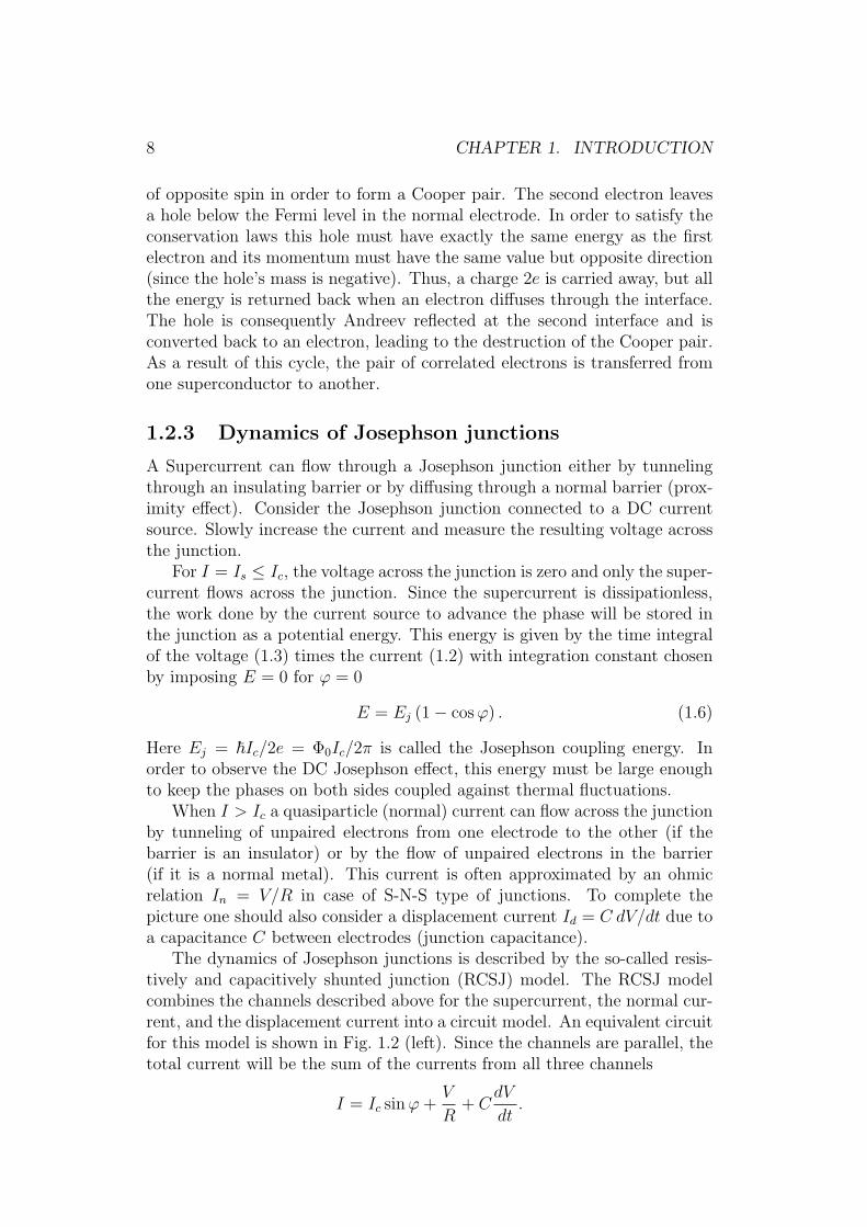
The dynamics of Josephson junctions is described by the so-called resis-tively and capacitively shunted junction (RCSJ) model. The RCSJ modelcombines the channels described above for the supercurrent, the normal cur-rent, and the displacement current into a circuit model. An equivalent circuitfor this model is shown in Fig. 1.2 (left). Since the channels are parallel, thetotal current will be the sum of the currents from all three channels
I = Ic sinφ+V
R+ C
dV
dt.

1.2. JOSEPHSON EFFECT 9
JR C
I=Ic
I=0
I=0.5Ic
I=1.5Ic
2E j
0
Ωp
Π 2 Π 3 Π 4 Πj
Fig. 1.2. Left: Equivalent circuit diagram for the RCSJ model. From left to right are theresistive, capacitive, and supercurrent channels. Right: Washboard potential of the RCSJmodel for different bias currents.
Using the AC Josephson relation this expression can be rewritten as
I = Ic sinφ+~
2eR
dφ
dt+
~C2e
d2φ
dt2. (1.7)
This equation describes the phase dynamics of the Josephson junction.When C is small the voltage across the junction at I > Ic can be found
from (1.7) (without the last term) and (1.3). This voltage is a periodicfunction of time
V (t) = RI2 − I2c
I + Ic cosωt,
where ω = 2eR√I2 − I2c /~.
Equation (1.7) can be considered as the equation of motion of a dampedand driven pendulum were C represents the moment of inertia, 1/R thedamping, and Ic the gravitation. The applied current I is the driving force.The natural frequency of the motion is given by the Jospehson plasma fre-quency
ωp(0) =√
(2eIc/~C).
This expression is only valid in the absence of an applied current. At a finitebias current, the Jospehson plasma frequency is
ωp(I) = ωp(0)(1− (I/Ic)2)1/4.
A qualitative insight into the junction dynamics can be obtained fromthe so-called tilted washboard model [Fig. 1.2 (right)]. It is also convenientto consider equation (1.7) as the equation of motion of a particle with aposition given by φ, a mass given by C, and a velocity given by φ. The

10 CHAPTER 1. INTRODUCTION
particle moves in the potential given by (1.6) minus the energy done bythe current source Esource = (~I/2e)φ, and is subjected to the viscous dragforce given by the conductance 1/R. The bias current I corresponds to theexternal force which tilts the potential. The kinetic energy of such a particleis equal to the energy CV 2/2 stored in the capacitive channel when thereis a time-varying voltage across the junction. In the case when I < Ic,the particle is confined to one of the potential minima, where it oscillatesback and forth at the plasma frequency. The time average of dφ/dt, andhence the time averaged voltage, is zero in this state. The local minima inthe washboard potential disappears and φ evolves in time when the currentI exceeds Ic. The dynamic case is associated with a finite voltage acrossthe junction which increases with increasing the bias current. The particlebecomes retrapped in one of the minima of the washboard when the biascurrent is reduced above Ic. The current at which it retrapps Ir dependson the inertial term given by C. There are two types of junctions namelyoverdamped and underdamped junctions. The particle has a small mass, andthus a small inertia, in the overdamped case and it becomes immediatelyretrapped at the current Ir = Ic. In contrast, it is necessary to reduce thecurrent to the retrapping current Ir < Ic in the underdamped case. Theparticle now has a large mass and can overshoot the minimum. This leads toa hysteretic current-voltage (I−V ) curve for an underdamped junction. TheMcCumber parameter βc is a measure of the degree of damping in a junction
βc = Q2 =2e
~IcR
2C,
where Q is the quality factor of the junction. The junction is overdampedwhen β . 1. In the opposite (underdamped) case, the energy stored in thecapacitor must be taken into account [33].
At I < Ic, the particle can escape from the potential well as a result of athermal activation (TA) process or macroscopic quantum tunneling (MQT).TA escapes from one potential well over the barrier to the next have a prob-ability ∼ e[−∆U(I)/kBT ] at each attempt. The attempt frequency is given bythe Jospehson plasma frequency. The barrier height ∆U(I) can be approx-
imated by ∆U(I) ≈ 2EJ (1− I/Ic)3/2. The probability for thermal escapes
is very small when kBT ≪ EJ and I ≪ Ic. As I approaches Ic, the barrierheight goes to zero and the probability of escapes from local energy minimarises exponentially. Once the particle overcomes the barrier by a thermalfluctuation, it can be either retrapped in the next potential well (for low Q)or continue to roll down the potential (for high Q), leading to a switching ofthe junction from the superconducting to the resistive state.
On the contrary, at a sufficient low temperature, the quantum tunneling isdominant and the escape process is characterized by quantum fluctuations.The motion of a particle moving in a tilted washboard potential can betreated as a simple harmonic oscillator in a well. Quantum mechanics shows

1.2. JOSEPHSON EFFECT 11
that there is a finite motion of the quantum oscillator (quantum fluctuation)at the lowest energy level. This leads to a finite tunneling amplitude throughthe barrier in a tilted washboard potential. The crossover from TA to MQTin underdamped Josephson junctions occurs at the crossover temperaturekBTcr ≈ ~ωp(I)/2π [34].
1.2.4 Magnetic properties of Josephson junctions
The important characteristic of a superconductor is that it screens magneticfields. The applied field will only penetrate a very short distance into asuperconductor, known as the London penetration depth λ, which is thecharacteristic length over which the magnetic field decays exponentially. If aJosephson junction is placed in an external magnetic field, its dynamics willbe altered because the field will penetrate a distance λJ into the junction.The Josephson penetration depth λJ is given by
λJ =
√Φ0c
8π2Jcdmagn[Si units: λJ =
√Φ0
2πJcµ0dmagn], (1.8)
where Jc is the critical current density and dmagn is the so-called magneticthickness. Since the Josephson currents are much weaker than the ordinarysuperconducting screening currents λJ ≫ λ. λJ is a very important charac-teristic since it determines the “magnetic size” of the junction. When thelength of the junction is smaller than λJ , the field will penetrate into thejunction uniformly and the junction is called “short”. If the length is biggerthan λJ , the flux dynamics of the junction starts to be important and thejunction is called “long”.
-3 -2 -1 0 1 2
1
Φ/Φ0
Imax
/Ic
L
H0
B
x x+ xd1
d2
t
zy
x
dl
Fig. 1.3. Left: Josephson junction in magnetic field H0. The thicknesses of two supercon-ducting electrodes are d1 and d2. Right: Simulated, according to (1.17), dependence ofthe maximum supercurrent on the external magnetic field.

12 CHAPTER 1. INTRODUCTION
Consider the “short” thin film type of Josephson junctions. The junctionis formed by two thin films which are separated by a barrier layer locatedwhere they overlap each other. The external magnetic field H0 is appliedin the y-axis direction perpendicular to the junction side L as it is shownin Fig. 1.3 (left). The thicknesses of two thin films d1,2 are of the order ofλ. In this case the field will completely penetrate the superconducting elec-trodes. The supercurrent density in the electrodes is given by the quantum-generalized second London equation [33]
J1,2 =c
4πλ2
(Φ0
2π∇θ1,2 −A
), (1.9)
where A is the magnetic vector potential. In the presence of a magnetic fieldin the barrier, the phase difference will have a gradient along the junctionlength L and can be found by integration of equation (1.9) over the infinites-imal contour of length 2dl, covering the barrier of thickness t ≪ d1,2 [Fig. 1.3(left)]∫
C1
∇ θ1 dl +
∫C2
∇ θ2 dl = θ1(x)− θ1(x+∆x) + θ2(x+∆x)− θ2(x) =
=2π
Φ0
(4πλ2
c
[J(x)2 − J
(x)1
]+Bt
)∆x.
Here J(x)1,2 are the x-components of the supercurrent density in the vicinity of
the barrier in the electrodes 1 and 2, and B is the in-plane (y-axis) magneticinduction in the barrier. Taking into account equation (1.1) and the definitionof derivative one can find
dφ(x)
dx=
2π
Φ0
(4πλ2
c
[J(x)2 − J
(x)1
]+Bt
). (1.10)
J(x)1,2 can be found from the Maxwell’s equation J1,2 = (c/4π)∇×H1,2, where
H1,2 is the field in electrodes 1 and 2 given by the second London equationfor the magnetic field in both electrodes
H1,2 + λ2∇×∇×H1,2 = 0. (1.11)
Taking into account the symmetry of the problem (H1,2 changes only in thez-axis direction), equation (1.11) can be rewritten as
d 2H1,2(z)
dz2=
H1,2(z)
λ2. (1.12)
Using the boundary conditions H1,2(0) = B and H1(d1) = H2(−d2) = H0,
J(x)1,2 can be calculated
J(x)1,2 =
c(±H0 cosh
[zλ
]∓B cosh
[d1,2∓z
λ
])cosech
[d1,2λ
]4πλ
, (1.13)

1.3. VORTICES IN TYPE II SUPERCONDUCTORS 13
anddφ(x)
dx=
2π
Φ0
(BΛ−H0S) . (1.14)
Here, Λ = t+ λ coth[d1λ
]+ λ coth
[d2λ
]and S = λ cosech
[d1λ
]+ λ cosech
[d2λ
].
When d1,2 . λ, screening by the electrodes is weak, B ≈ H0, and (1.14) canbe simplified to
dφ(x)
dx=
2πH0
Φ0
dmagn, (1.15)
where
dmagn =
(t+ λ tanh
[d12λ
]+ λ tanh
[d22λ
])(1.16)
is the magnetic thickness for thin films. Therefore thin film junctions are lesssensitive to magnetic field [35].
Integration of (1.15) gives φ(x) = (2πH0/Φ0)dmagnx + C, and, using
the DC Josephson relation, the total maximum supercurrent through thejunction is
Imax = Ic
∣∣∣∣sin(πΦ/Φ0)
πΦ/Φ0
∣∣∣∣ , (1.17)
where Φ = H0Ldmagn is the total magnetic flux through the junction. Imax is
the periodic function of Φ/Φ0 and is equal to zero when the total magneticflux is equal to an integer number of Φ0. Such a diffraction pattern is calledthe Fraunhofer pattern [Fig. 1.3 (right)] in analogy to diffraction of lightthrough a slit.
1.3 Vortices in type II superconductors
There are two classes of superconductors, depending oh their response to anexternal magnetic field: type I and type II. For type I superconductors, themagnetic field cannot penetrate inside the material, showing the Meissnereffect, up to some critical field Hc at which a first order superconducting-to-normal phase transition takes place. Unlike type I superconductors, typeII superconductors have intermediate range between two critical fields, Hc1
and Hc2, where they remain superconducting but allow magnetic field insidethe material in form of Abrikosov vortices. The field Hc1 is a characteristicof the particular material. Upon increasing the field further, the magneticflux density gradually increases. Finally, at Hc2 the superconductivity isdestroyed.
Each vortex consists of a region of circulating supercurrent around asmall non-superconducting core. The magnetic field is able to pass throughthe sample inside the vortex core. Each vortex carries a flux quantum, Φ0 =hc/2e. For type II superconductors λ/ξ > 1/
√2, where λ is the magnetic
penetration depth and ξ is the superconducting coherence length representingradius of non-superconducting vortex core.
14 CHAPTER 1. INTRODUCTION
L
2-nd electrode
z
x
L
2-nd electrode
zV
Abrikosovantivortex
V
xV
V
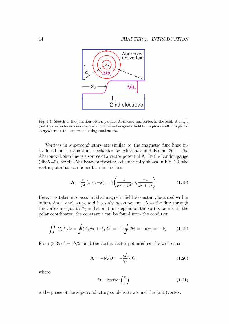
Fig. 1.4. Sketch of the junction with a parallel Abrikosov antivortex in the lead. A single(anti)vortex induces a microscopically localized magnetic field but a phase shift Θ is globaleverywhere in the superconducting condensate.
Vortices in superconductors are similar to the magnetic flux lines in-troduced in the quantum mechanics by Aharonov and Bohm [36]. TheAharonov-Bohm line is a source of a vector potentialA. In the London gauge(divA=0), for the Abrikosov antivortex, schematically shown in Fig. 1.4, thevector potential can be written in the form
A =b
r2(z, 0,−x) = b
(z
x2 + z2, 0,
−x
x2 + z2
)(1.18)
Here, it is taken into account that magnetic field is constant, localized withininfinitesimal small area, and has only y-component. Also the flux throughthe vortex is equal to Φ0 and should not depend on the vortex radius. In thepolar coordinates, the constant b can be found from the condition∫∫
Bydxdz =
∮(Axdx+ Azdz) = −b
∮dΘ = −b2π = −Φ0 (1.19)
From (3.35) b = c~/2e and the vortex vector potential can be written as
A = −b∇Θ = −c~2e
∇Θ, (1.20)
where
Θ = arctan(xz
)(1.21)
is the phase of the superconducting condensate around the (anti)vortex.

1.4. INTRODUCTION TO FERROMAGNETISM 15
1.4 Introduction to ferromagnetism
1.4.1 Basic concepts
Ferromagnetism is magnetically ordered state in which the majority of atomicmagnetic moments are oriented in one direction. Consequently, the ferro-magnetic state is characterized by a net spontaneous magnetization M i.e. amagnetization even in zero external field. Ferromagnetism occurs at temper-ature below the Curie temperature TC in the absence of external field. Uponapplication of a weak magnetic field, the magnetization increases rapidly toa high value called the saturation magnetization. Ferromagnets tend to staymagnetized to some extent after being subjected to an external magneticfield. This tendency to “remember magnetic history” is called hysteresis.The fraction of the saturation magnetization which is retained when thedriving field is removed is called the remanence of the material.
The first successful attempt to explain magnetic ordering was made by P.Weiss. He postulated that a ferromagnet is composed of small spontaneouslymagnetized regions (domains) and the total magnetic moment is the vectorsum of the magnetic moments of the individual domains. Each domain isspontaneously magnetized because of a strong internal (molecular) magneticfield which is proportional to M . The effective field acting on any magneticmoment within the domain may be written as H = H0 + αM , where H0 isexternal field and αM is the Weiss molecular field.
A quantitative description of ferromagnetism requires a quantum theorytreatment. The important consequence of the Pauli exclusion principle is thedependence of the energy of a system of fermions (electrons) on the total spinof a system. This can be explained by existence of an additional exchangeinteraction. The exchange interaction appears when the wave functions ofneighboring electrons overlap (direct exchange). The exact expression foran exchange interaction cannot be obtained even in the simplest case oftwo-electron system. There are different approximations to the exchangeinteractions exist. One of the simplest is the Heisenberg Hamiltonian
Hex = −∑i =j
JijSiSj.
This interaction favors parallel orientation of the spin magnetic moments Si
and Sj if the parameter Jij > 0 and antiparallel spin orientation if Jij < 0.The exchange interaction has an electrostatic origin and depends on themutual spin orientation of the electrons in the system, and is responsible forthe magnetic ordering.
Magnetic ordering occurs only in materials which have unfilled electronshell (orbital) in the atoms. Only non saturated internal electronic shells(i.e. those protected to form chemical bonds by shells further out from thenucleus) can remain unfilled when an atom incorporated in a multiatomic

16 CHAPTER 1. INTRODUCTION
system. Such unfilled shell creates a non-zero total magnetic moment. Thetotal magnetic moment is the sum of the spin and the orbital momentum ofthe electrons. For 3d transition metals, such as Ni, Fe, Co, etc., the totalmagnetic moment is largely determined by the spin moment.
There are two models of magnetism. The first assumes that the magneticelectrons are localized at the atomic sites, and can be found in states thatare similar to the free atom. This is the model of magnetism of localizedelectrons. On the other hand, the model of itinerant electrons states that themagnetic electrons are the conduction electrons which are totally delocalize,and free to travel anywhere in the sample. In this case, the magnetic momentcarried by a magnetic atom differs markedly from the free atom. The firstmodel well describes the rare earth metals (4f) while second is appropriatein case of metals and alloys of the 3d transition series.
The magnetic moments of the rare earth metals are associated both withthe spin and the orbital angular momentum of the f electrons. The f elec-trons have small spatial extension making them weakly sensitive to theirlocal environment. The s or d electrons delocalize to some extent to becomeconduction electrons. Typically, the spatial extension of f electrons is far lessthan the interatomic distances, and correspondingly there can be no direct in-teraction between f electrons of different atoms. Rather, it is the conductionelectrons which couple the magnetic moments. The conduction electron ispolarized when interacting with a localized magnetic moment. The electronpasses to the next localized magnetic moment and interacts with it. Thusthe two localized magnetic moments are correlated. This type of indirectexchange mechanism is called the Ruderman-Kittel-Kasuya-Yosida (RKKY)exchange.
In case of 3d transition metals, the localized magnetic moment is carriedby d electrons. These electrons are not very much affected by the lattice,but they overlap a little with the orbitals of neighboring atoms forming aconduction band. The ferromagnetic state arises from a difference in theoccupation of the bands with spin up and down. This can happen in somecases when energy is minimized upon transferring of some electrons fromone spin state to the other. The main reason for this comes from the Pauliexclusion principle, which postulates that two electrons with the same spincan never be in the same “place” at the same time. This means that twoelectrons with opposite spins will repel each other more than two electronswith the same spin, as the latter feel each other less because they can never bein the same place. The criterion for instability with respect to ferromagnetismis IN(EF ) > 1, where I is the difference in repulsion energy between electronswith opposite spins and electrons with the same spin direction, and N(EF )is the density of electron states at the Fermi level. This criterion is calledStoner criterion. Note that this criterion shows that strength of ferromagneticmetals is largely depend on the density of states at the Fermi level [37].

1.4. INTRODUCTION TO FERROMAGNETISM 17
0.0 0.2 0.4 0.6 0.8 1.00.00
0.05
0.10
0.15
xy (
cm)
H (T)
MsatR1
Fig. 1.5. Behavior of the Hall resistivity ρxy as a function of magnetic field in ferromagnet.Two contribution from the ordinary Hall effect and from spontaneous magnetization canbe distinguished.
1.4.2 Anomalous Hall effect
Ordinary Hall effect (OHE) results in appearance of transverse resistivityρxy = Ey/jx when magnetic field H is applied perpendicular to a plate witha current flowing in longitudinal direction. This is a consequence of theLorentz force acting on charge carriers which gives rise to the electric field inthe transverse direction Ey. The ordinary Hall resistivity is a linear functionof applied magnetic field ρxy = R0H, where R0 is called ordinary Hall coeffi-cient, which depend on a charge density. However, magnetic materials suchas ferromagnets show different response of the Hall resistivity on the externalmagnetic field, as shown in Fig. 1.5. Initially, the Hall resistivity increasesrapidly with magnetic field up to some saturation value. After saturation, theHall resistivity increases linearly with much smaller gradient. The Hall effectin this case does not arise only from the Lorenz force acting on the chargecarriers. It is called the anomalous Hall effect (AHE) [38, 40]. The behaviorshown in Fig. 1.5 can be regarded as having two contributions: first is theordinary Hall effect with a behavior expected from a consideration of theLorenz force, and second is proportional to the spontaneous magnetizationM [38, 39]
VH = (ρxyIx)/d = (R0H +R1M)I/d. (1.22)
Here VH is the Hall voltage, Ix is the applied current, d is the film thickness,and R1 is the extraordinary Hall coefficient. The coefficient R1 may be oneto two orders higher than R0 and has strong temperature dependence.
The AHE may have both extrinsic and intrinsic contributions [40]. Theextrinsic contribution is due to spin-orbit coupling. It involves two impurity

18 CHAPTER 1. INTRODUCTION
scattering mechanisms, skew scattering [41, 42] and side jump [43], which givedifferent scattering directions depending on spin orientation of the chargecarriers. As a consequence, the spin-up carriers will scattered to one side ofthe plate and spin-down to opposite side. There is an imbalance betweenspin-up and spin-down charge carriers in ferromagnetic materials. This willlead to a charge accumulation at one of the side creating a transverse electricfield and leading to the anomalous Hall effect.
The intrinsic contribution arises from finite effective magnetic flux, as-sociated with the Berry phase [44]. A charge carrier acquires an additionalphase, called the Berry phase, when its spin follows the local magnetizationdirection within the plate, by analogy to the parallel transport of a vectoralong closed path on a sphere [45]. The effect of this Berry phase can beseen as effective magnetic flux applied perpendicular to the plate. Hence,the spatially varying magnetization and its related Barry phase can induceHall effect in the absence of an external magnetic field.
To make things clear for the following discussions it is convenient to pointout some difference in definitions which are in use in the literature. The AHEcombines both the OHE, which is related only to external magnetic field,and the extraordinary Hall effect (EHE). The last is related to spin-orbitcoupling and/or Berry phase as well as to the Lorenz force from intrinsicmagnetization of ferromagnet. The spontaneous Hall effect is related only tospin-orbit coupling and/or Berry phase.
Magnetic alloys have been reported to show anomalously large EHE [46,47, 48, 49], which is two orders of magnitude larger than for magnetic el-ements such as Fe, Co and Ni [50]. The EHE provides a very simple wayof studying magnetic properties of thin films, compared to other measure-ment techniques such as vibrating sample magnetometer [51], superconduct-ing quantum interference device magnetometer [103], optical [53] and Hallprobe magnetometer [54]. The reciprocal dependence of the measured Hallvoltage on the film thickness, see equation (1.22), makes this technique pref-erential for analysis of thin films. The EHE allows us to study magneticproperties at all temperatures and magnetic fields [55].
1.4.3 Magnetism in thin film structures
Magnetic properties of thin films can be quite different from that for thebulk material. The magnetism of metals is very sensitive to the local atomicenvironment. This environment influences both the strength and sign of theexchange interaction, and it determines the local anisotropy of the material.The atomic environment at the surface of a material, or at the interface be-tween two different materials, is strongly modified in comparison to the bulkmaterial. At a surface the number of neighbors is reduced and, moreover, thesymmetry is not the same as for the bulk material. Obviously, any surfaceeffect may have a substantial impact on the properties of a thin film.
1.4. INTRODUCTION TO FERROMAGNETISM 19
The magnetic moment of ferromagnetic transition metals is predicted tobe higher at the surface than in the bulk. This is due to a narrowing of thed-band because of the lower number of atom’s neighbours. This results inan increase of the density of states N(EF ) at the Fermi level. In the transi-tion metals which are characterized by itinerant magnetism, the increase ofN(EF ) leads to an increase of the surface magnetism (Stoner criterion).
The magnetic properties of the thin films may also depend on the na-ture of the substrate. If the cell matching between the substrate and thedeposited film is not perfect, both materials will be deformed depending ontheir respective rigidness and thicknesses. This results in a variation of thecell parameter of the deposited material causing a change in its magneticproperties. Contraction of the cell results in a reduction in the magneticmoment while a dilation of the cell tends to increase the magnetic moment.The choice of substrate can also influence the electronic structure of the de-posited film. Certain substrates have little or no direct electronic interactionwith the deposited films, while the use of others leads to hybridization effectsbetween the electrons of the magnetic film and those of the substrate.
The ordering temperature of ferromagnetic materials (the Curietemperature) is given by
TC = J0S(S+1)/3kB,
where S is the value of an individual atom’s spin, and J0 is the sum of theexchange interactions with all neighbours. According to this expression, TC
is proportional to the number of neighbours. Therefore one can expect areduction in the ordering temperature at the surface of a ferromagnetic ma-terial. This is true in a number of real cases where one then refers to thecreation of dead layers at interfaces and surfaces. However, in certain casesthe dominant effect is not a reduction but an increase in the ordering tem-perature at the surface. For transition metals, this is again due to increaseof N(EF ). This strengthens the magnetic stability at the surface accordingto the Stoner criterion.
Magnetic anisotropy is the dependence of the magnetic energy of asystem on the direction of magnetization within the sample. Thin filmsshow very large anisotropy which may be very complex, since the strengthof magnetic anisotropy of thin films can be affected by composition and/orfabrication conditions. Moreover, the absence of preferred crystallographicorientation in polycrystalline thin films makes it difficult to control the mag-netic anisotropy. For thin films, the shape usually favors an orientation ofmagnetization within the plane in order to minimize the energy. This energy

20 CHAPTER 1. INTRODUCTION
is often described by a uniaxial anisotropy
E = −K cos2 θ,
where θ is the angle between the magnetization and the normal to the planeof the sample. By definition, a positive value of K implies an easy axisof magnetization perpendicular to the plane of the sample (θ = 0) while anegative value of K corresponds to an easy plane of magnetization (θ = π/2).There are different sources of magnetic anisotropy in thin films. They canbe divided into two groups, those related to the volume of the material (Kv),and those related to its surface or interface (Ks). The anisotropy of a thinfilm of thickness t is given by K = Kv + Ks/t [37]. The reorientation ofthe easy axis of magnetization from in-plane to out-of-plane, as a function ofthe film thickness and temperature, has been observed in a large number oftransition metal thin films and multilayers [56, 57, 58, 59, 60, 61, 62, 63].
As it was mentioned in section 1.1, in this work the Hall effect is em-ployed for analysis of magnetic properties of the Pt1−xNix thin films. Byusing the Hall effect it is possible to determine the easy axis of uniaxialmagnetic anisotropy [64, 65, 66]. For the out-of-plane orientation of theeasy axis, magnetization of the film in the perpendicular field will have ahysteresis/coercivity and so will Hall resistance. However, for the in-planeorientation of the easy axis, the magnetization of the film in perpendicularmagnetic field will have zero coercivity, because in this case only rotation ofmagnetization takes place without translational movement of magnetic do-main walls [65].
Magnetic thin films often exhibit superparamagnetism [67, 68], whichis not common for bulk materials. In the supermagnetic state the systembehaves not like one single domain particle with all its moments aligned inone direction, but rather splits into multiple magnetic domains (clusters). Athigh temperatures the direction of magnetization of each domain fluctuatesand eventually freezes below the so-called blocking temperature Tb, belowwhich the system can exhibit a spontaneous magnetization. Superparamag-netism differs from conventional paramagnetism because the effective mag-netic moment of the particle is the sum of its ion constituents and can beseveral thousand Bohr magnetons [68].
1.4.4 Theory of PtNi alloys
PtNi is an interesting alloy both from fundamental and technological pointsof view due to non-trivial magnetic and catalytic properties [28, 29]. Pt ischaracterized by the strong spin-orbit interaction, which leads for example tothe appearance of a large spin-Hall effect [69, 70]. When mixed with magneticelements, like Ni or Fe, Pt provides a non-trivial host matrix, which leadsto a large variety of physical properties among magnetic binary alloys of Pt.

1.4. INTRODUCTION TO FERROMAGNETISM 21
Detailed understanding of those properties remain a serious theoretical chal-lenge, which is further complicated by existence of different ordered phases,showing different properties compared to disordered alloys [71, 72, 73, 27].PtNi together with PdNi are the two known binary Ni alloys that form solidsolutions at arbitrary proportions [25, 71]. However, while PdNi becomes fer-romagnetic at very low Ni concentration, the onset of zero temperature fer-romagnetism in bulk PtNi occurs at fairly large Ni concentration [25, 27, 74],which makes it easier to control the composition, material and magneticproperties.
The magnetic moment distribution in bulk PtNi alloys was studied quiteexhaustively by high field susceptibility measurements [26], magnetization [74]and by neutron scattering experiments [76]. It was observed that PtNi alloysindeed are spatially uniform, in contrast to CuNi and many other Ni andFe based binary alloys, which are prone to phase segregation [26]. The bulkPtNi alloy can exist in two phases: a chemically disordered face centered cu-bic (fcc) with Pt and Ni atoms randomly distributed over the crystal lattice;and a chemically ordered state, either with face centered tetragonal (fct) orfcc structure, depending on Ni concentration [71]. The concentration depen-dence of the magnetic moment and the Curie temperature is different for theordered and disordered alloys, especially at low Ni concentrations [74, 27, 75].
Both experimental and theoretical analysis of the local magnetic momentfor disordered alloys show that the magnetization decreases monotonicallywith a decreasing Ni concentration. The zero temperature magnetizationvanishes at a Ni concentration around 40 at.%. The structure is fcc withoutany distortion for all Ni concentrations, but any short-ranged ordering hasa great impact on the local Ni magnetic moment. The magnetism of Ni inalloys strongly depends on its near environment. For example, if Ni is notsurrounded by at least six other Ni in a fcc lattice, then it loses its mag-netic moment altogether at any temperature. Thus the effect of environmentshould be taken into account while considering the local magnetic momentof Ni [27].
There is a tetragonal distortion of the lattice in ordered alloys at about50 at.% concentration of Ni. The tetragonal distortion increases the Ni-Nidistance leading to a self-dilution in this system. This results in vanishingof the local magnetic moment on Ni at this concentration as it was experi-mentally observed in [77, 27]. However, the theoretical analysis given in [27]predicts reasonably large magnetic moments on Ni at 25 at.% concentrationof Ni. The alloy at this concentration has a fcc structure without tetragonaldistortion.
22 CHAPTER 1. INTRODUCTION
1.5 S-F-S Josephson junction
1.5.1 Origin of order parameter oscillation in S-F bi-layer
Superconducting correlations induced in the ferromagnet differ from thosein S-N proximity systems. In a normal metal, the destruction of Cooperpairs is due to thermal fluctuations (characteristic energy E = kBT ). Incase of a S-F system, there is one more depairing factor in the ferromagnet,namely the exchange energy Eex. The exchange energy will try to orient allspins in one direction. This will destroy the Cooper pair which forms fromelectrons with opposite spins. Thus the length scale on which the Cooperpair can penetrate the ferromagnet is also affected by Eex. Moreover, thesuperconducting order parameter displays an oscillatory behavior under theinfluence of the exchange energy of the ferromagnet.
The exchange energy is the main depairing factor if the Curie temper-ature TC is much higher than the superconducting critical temperature Tc
(Eex ≫ kBT ). In this case and for a “dirty” ferromagnet, the Cooper paircan penetrate the ferromagnet up to a distance ξF1 = (~D/Eex)
1/2. Here Dis the diffusion coefficient in the ferromagnet layer. The order parameter willoscillate with an oscillation period of 2πξF2 , where ξF2 = ξF1 .
In case of Eex > kBT , ξF1 and ξF2 are not equal and can be written as [11]
ξF1,2 =
√~D(
(πkBT )2 + E2
ex
)1/2 ± πkBT. (1.23)
Expression (1.23) is valid for a “dirty” ferromagnet.A qualitative picture of the appearance of the order parameter oscillation
can be obtained for “clean” metals in the framework of quantum mechanics.In the S-F bilayer the correlated electrons in the pair having opposite spindirections experience the exchange field of the ferromagnet, resulting in theappearance of a net nonzero momentum Q of the Cooper pair [78]. Con-sider the Cooper pair formed by two electrons with opposite (lying on theFermi surface) momentums pF and −pF , so that the total momentum of thepair equal to zero. Under the influence of Zeeman interaction only, the singleparticle Hamiltonian for an electron with a spin can be written as
H =p2
2m− e~
2mc(σ · h),
where h is the exchange field. The corresponding two classical Hamiltoniansfor electrons with spin up and spin down are
H↑ =p2
2m− Eex, H↓ =
p2
2m+ Eex. (1.24)

1.5. S-F-S JOSEPHSON JUNCTION 23
h
p1
p2
pF
- pF
S
p1
p2
p+ pDF
- p+ pDF
F
z
x
p1
p2
pF
- pF
S
p1
p2
p p-DF
- p p-DF
F
(a)
(b)
Fig. 1.6. Appearance of the nonzero net momentum in the ferromagnet close to S-Finterface under an exchange field h. (a) and (b) correspond to different spin configurationsof electrons in pair. Adopted from [78].
Consider the one dimensional case when the electrons forming the Cooperpair may change their momentums in the x direction only. According to(1.24), the spin up electron in the pair lowers its energy by Eex and the spindown electron raises its energy by the same amount upon entering the Fregion. In order for each electron to conserve its total energy, and thus keepthe Copper pair, the spin up electron must increase its kinetic energy whilethe spin down must decrease. Because kinetic energy depends only on themomentum, a change of energy means change the momentum. Consider thecase when an electron with momentum p1 has a spin down and an electronwith momentum p2 has a spin up [Fig. 1.6(a)]. Then, the kinetic energiesfor electrons with momentums p1 = −pF and p2 = pF in the F region can bewritten as
E↓1 =
(−pF +∆p1)2
2m=
p2F2m
− pF∆p1m
+∆p212m
=(−pF )
2
2m− Eex
E↑2 =
(pF +∆p2)2
2m=
p2F2m
+pF∆p2m
+∆p222m
=(pF )
2
2m+ Eex.
(1.25)
Taking into account that ∆p ≪ pF , from (1.25) each electron acquires a pos-itive gain in momentum p1,2 = Eex/υF . Here υF = pF/m is the Fermi ve-

24 CHAPTER 1. INTRODUCTION
locity. The Cooper pair as a whole acquires the momentum Q = 2Eex/υF .As a result it starts to move in the positive direction from the S-F interface.Then, the wave function of the pair acquires an additional exponential factorand can be written as
Ψa(x) = ΨF (x) exp
(i2Eex
~υFx
),
where ΨF (x) = Ψ0 exp (−x/ξF1) describes the damping of the superconductororder parameter by analogy with the S-N proximity effect and Ψ0 is the orderparameter at the S-F interface.
In the opposite case, the electron with momentum p1 has the spin up andelectron with momentum p2 has the spin down [Fig. 1.6(b)]. In this case,both electrons acquire a negative gain in momentum p1,2 = −Eex/υF . TheCooper pair as a whole acquires the momentum Q = −2Eex/υF and thewave function can be written as
Ψb(x) = ΨF (x) exp
(−i2Eex
~υFx
).
Since states Ψa(x) and Ψb(x) are equally probable, the real state will be asuperposition of these states
Ψ(x) =1
2(Ψa(x) + Ψb(x)) = Ψ0 exp
(− x
ξF1
)cos
(2Eex
~υFx
).
It is seen that the superconducting order parameter is a decaying oscillatoryfunction (Fig. 1.7). The wavelength of such oscillations is
λ =π~υFEex
,
which gives ξF2 = ~υF/2Eex for a clean ferromagnet.One should bear in mind that the picture described above is purely qual-
itative. It implies continuity of the order parameter at the S-F interface.This corresponds to a very weak ferromagnet with an extremely small ex-change energy. Other drawbacks are the temperature independence and thedescription of the Cooper pair by the common wave function. To get a morecorrect picture one should consider the correlation of independent electronsrather than the Cooper pair as one whole.
1.5.2 Theory of S-F-S π junction
To describe the relevant experimental situation one needs to use a micro-scopic approach. The main objects of this approach are the Bogoliubov-deGennes equations or the Green’s function technique which describe correla-tion between electrons with parallel and antiparallel spins. These equations

1.5. S-F-S JOSEPHSON JUNCTION 25
S F
l
Fig. 1.7. Schematic picture of the order parameter oscillations in a S-F bilayer. The realpart of the order parameter is the decaying oscillatory function.
can be reduced to the Eilenberger [79] equations by averaging with respectto the relative electron motion in the pair. The Eilenberger equations canbe further simplified to the Usadel [80] equations in case when the electronmean free path is small (diffusive approximation) and the ferromagnet is un-perturbed by the proximity with the superconductor (the pairing potential∆ is absent in the ferromagnet).
In the “clean” limit the critical current of the S-F-S junction can bewritten as [81]
IcRn =π∆2
4e
|sin (4Eextf/~υF )|4Eextf/~υF
, (1.26)
whereas in the case of the diffusive (“dirty”) limit, the critical current isgiven by
IcRn =π∆2
4eTc
4y
∣∣∣∣cos(2y) sinh(2y) + sin(2y) cosh(2y)
cosh(4y)− cos(4y)
∣∣∣∣ , (1.27)
where y = tf/ξF , tf is ferromagnet barrier layer thickness, Rn is the normalstate resistance of the junction, and ξF ≡ ξF2 = (~D/Eex)
1/2 [82]. In the“clean” limit the critical current decays as ξF/tf while in the diffusive limitit decays exponentially as e−tf/ξF .

26 CHAPTER 1. INTRODUCTION

Chapter 2
Experimental methods
2.1 Sample fabrication
Different micro/nano fabrication techniques were used in the sample fabri-cation process. In this section the most important of them will be describedand we will go through all steps required for samples fabrication. Most ofthe fabrication steps were done in the AlbaNova nanofabrication lab at theCore Facility in Nanotechnology, Stockholm University.
2.1.1 Film deposition
All multilayered structures and single films used in this work were depositedby DC magnetron sputtering. Sputtering is the most widely used laboratorytechnique for preparing thin films. The majority of sputtering machinesworks with a base pressure of 10−8 to 10−6 mbar. An inert gas, usually Ar,is introduced into the chamber in a controlled manner, and maintained at apressure between 5 · 10−4 and 2 · 10−2 mbar. The gas is ionized in a strongelectric field creating a plasma. The positive Ar ions are attracted towards atarget of the material to be deposited. The bombardment of the target withthese relatively heavy ions results in atoms being torn out of the target, i.e.sputtered away. These atoms travel through the plasma and the neutral gas,and condense on a wafer. In the case of metallic targets, the ions are attractedto the target by applying a constant negative voltage to the target (DCsputtering). In magnetron sputtering systems, the field lines of permanentmagnets placed behind the target act to channel the electric charges, andthus concentrate the plasma in the vicinity of the target, resulting in theincreased sputtering rate.
Before starting the sputtering process, the oxidized Si wafer was cleanedin oxygen plasma over 10 min with the RF power of 50 W in order to removeorganic contamination and therefore to improve the adhesion between waferand material to be sputtered.
27

28 CHAPTER 2. EXPERIMENTAL METHODS
N S N
Ar+
Ar+
Electrons
Anode
Substrate
Magnetic lines
Cathode(target)
15 cm
DCpowersupply
-
+
Ar+
Ar+
3.75 cm
N S N
(a) (b)
6cm
10
cm
DCpowersupply
-
+
Fig. 2.1. Scheme of the sputtering setup for Nb (a) and Pt1−xNix (b) depositions. Theoff-axis displacement between the target and the wafer creates the thickness gradient from20 nm to 30 nm, in the middle of wafer, for Pt1−xNix thin film.
S-F-S multilayers and test ferromagnetic single-layers
The Nb-Pt1−xNix-Nb-Pt1−xNix multilayers were sputtered in a single vacuumcycle with the base pressure about 10−6 mbar. The Ar pressure was main-tained at 9.3 · 10−3 and 6.7 · 10−3 mbar during Nb and Pt1−xNix sputteringrespectively. This provides mean free path of about 2.3 cm for Nb and 3.2cm for Pt1−xNix. The lower and upper Nb layers were sputtered with thesmallest distance (6 cm) between the 6” Nb target and wafer and the DCpower of 0.35 kW for over 3 min 15 sec and 5 min for lower and upper layersrespectively. The Nb deposition rate was estimated prior, using the lift-offprocess, to 11.5 A/sec. Thus the thicknesses of lower and upper layers of Nbexpected to be 225 and 350 nm respectively. The smallest distance betweenthe target and wafer during deposition and high deposition rate for Nb werechosen to provide the highest Tc.
The layers of Pt1−xNix were sputtered at the maximum distance (10 cm)from the 1.5” target to the wafer and the DC power of 0.05 kW with sput-tering rate of 1.67 A/sec for over 3 min.
The edge of the 2” wafer was positioned just under the target center as itis schematically shown in Fig. 2.1(b). This does not cause any problems withuniformity on Nb deposition, since the target is large (6” diameter) [see thescheme in Fig. 2.1(a)]. On the other hand, such off-axis displacement createsthe thickness gradient from 20 nm to 30 nm in the middle of wafer, forPt1−xNix, since the target is only 1.5” diameter. Therefore, S-F-S junctionswith different F-layer thickness but the same Ni-content could be made lateron from the different parts of the same wafer.
The left panel in Fig. 2.2 shows the Scanning Electron Microscope (SEM)image of the deposited multilayer side view from which the thicknesses ofupper and lower layers of Nb can be verified. The right panel in Fig. 2.2 shows
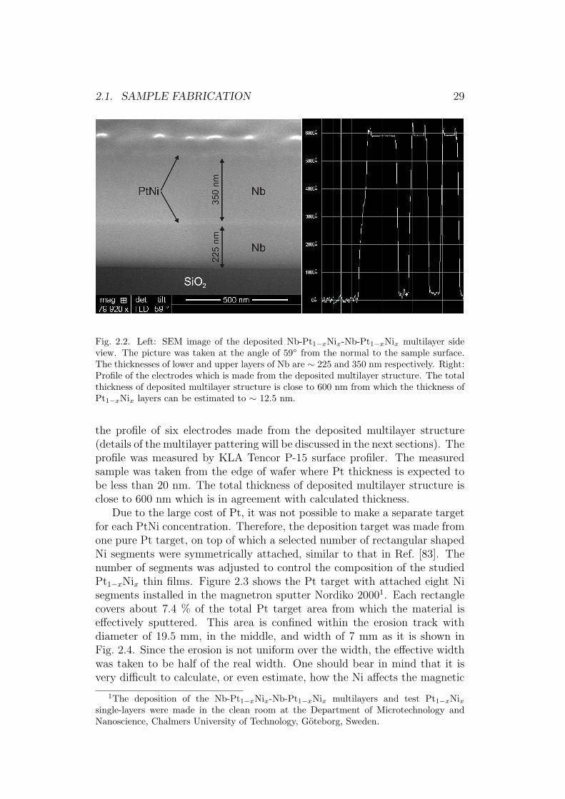
2.1. SAMPLE FABRICATION 29
Fig. 2.2. Left: SEM image of the deposited Nb-Pt1−xNix-Nb-Pt1−xNix multilayer sideview. The picture was taken at the angle of 59 from the normal to the sample surface.The thicknesses of lower and upper layers of Nb are ∼ 225 and 350 nm respectively. Right:Profile of the electrodes which is made from the deposited multilayer structure. The totalthickness of deposited multilayer structure is close to 600 nm from which the thickness ofPt1−xNix layers can be estimated to ∼ 12.5 nm.
the profile of six electrodes made from the deposited multilayer structure(details of the multilayer pattering will be discussed in the next sections). Theprofile was measured by KLA Tencor P-15 surface profiler. The measuredsample was taken from the edge of wafer where Pt thickness is expected tobe less than 20 nm. The total thickness of deposited multilayer structure isclose to 600 nm which is in agreement with calculated thickness.
Due to the large cost of Pt, it was not possible to make a separate targetfor each PtNi concentration. Therefore, the deposition target was made fromone pure Pt target, on top of which a selected number of rectangular shapedNi segments were symmetrically attached, similar to that in Ref. [83]. Thenumber of segments was adjusted to control the composition of the studiedPt1−xNix thin films. Figure 2.3 shows the Pt target with attached eight Nisegments installed in the magnetron sputter Nordiko 20001. Each rectanglecovers about 7.4 % of the total Pt target area from which the material iseffectively sputtered. This area is confined within the erosion track withdiameter of 19.5 mm, in the middle, and width of 7 mm as it is shown inFig. 2.4. Since the erosion is not uniform over the width, the effective widthwas taken to be half of the real width. One should bear in mind that it isvery difficult to calculate, or even estimate, how the Ni affects the magnetic
1The deposition of the Nb-Pt1−xNix-Nb-Pt1−xNix multilayers and test Pt1−xNixsingle-layers were made in the clean room at the Department of Microtechnology andNanoscience, Chalmers University of Technology, Goteborg, Sweden.

30 CHAPTER 2. EXPERIMENTAL METHODS
Fig. 2.3. Pt target with 8 attached rectangular shaped Ni segments providing the totaleffective deposition area of Ni about 59.2 %.
Fig. 2.4. 1.5” Pt target. The position of rectangular shaped Ni segment with the size4.5 × 14 mm is shown schematically. The erosion track has the diameter of 19.5 mm, inthe middle, (shown by blue circle) and width of 7 mm. The rectangular shaped Ni segmentcovers ∼ 7.4% of the total Pt target area from which the material is effectively sputtered.The region, from which the material is effectively sputtered, is confined within two dashedcircles.
2.1. SAMPLE FABRICATION 31
field and thereby the deposition rate. The real concentration of Ni in the filmdeposited from the target, shown in Fig. 2.3, corresponds to about 54 at.%of Ni. The details of determination of Ni concentration will be discussed insection 3.1.
The deposited structure consists of two Nb layers separated by Pt1−xNixlayer. One additional layer of Pt1−xNix was deposited on top of the upper Nblayer as it is shown in Fig. 2.2. The intermediate layer of Pt1−xNix was usedas the junction barrier, while the upper layer was used for improving adhesionwith bonding contacts. Initially, Au was used, instead of Pt1−xNix, as thecontact layer (upper layer). However, it turned out that the deposition of Auon top of Nb-Pt1−xNix-Nb trilayer is inadmissible in case when anodizationis needed (see subsection 2.1.4).
In addition, test Pt1−xNix single-layers were deposited on oxidized Siwafer for analysis of ferromagnetic properties of Pt1−xNix alloys. The filmswere deposited with the same parameters as the Pt1−xNix layers implementedin the Nb-Pt1−xNix-Nb-Pt1−xNix multilayers but without the of-axis displace-ment. The deposition time was about 5 min providing the thicknesses ofPt1−xNix single layers in the range between 50 and 60 nm.
F-S and N-S bilayers
Cu0.47Ni0.53-Nb bilayers were deposited on oxidized Si substrates by RF andDC magnetron sputtering, respectively2. The Cu0.47Ni0.53 alloy has the CurieTC temperature ∼ 60 K and the coherence length ξF ∼ 2-7 nm. The thick-nesses of the CuNi and Nb layers are 50 and 70 nm respectively.
The critical temperature Tc of a superconducting thin film can be quitesensitive to the deposition conditions. To check Tc of the Nb layer embeddedin the Cu-Nb bilayers, the resistance as a function of temperature has beenmeasured for the films deposited at different process pressures and DC pow-ers. The Nb films were deposited by combination of RF and DC magnetronsputtering. Figures 2.5 (a), (b), and (c) show R(T ) dependencies of the filmsdeposited at a DC power of 167 W, 203 W, and 253 W respectively. Arprocess pressure was varied from 5 to 10 mTorr for each DC power, and aRF power of 5 W was kept always the same. One can see that the highestTc together with the lowest normal state resistance were obtained at the DCpower of 253 W and Ar pressure of 5 mTorr. The deposited final structureconsists of Cu layer with the thickness of 50 nm, deposited at a DC power of132 W and Ar pressure of 3 mTorr, covered by Nb layer with the thicknessof 70 nm. To protect the Nb layer from oxidation, thin layer of Cu with thethickness of 11 nm was deposited on top.
2The deposition of the Cu0.47Ni0.53-Nb bilayers and magnetic characterization of theCu0.47Ni0.53 alloy were done by V. A. Oboznov and V. V. Ryazanov at Institute of SolidState Physics, Chernogolovka, Russian Federation.

32 CHAPTER 2. EXPERIMENTAL METHODS
8.0 8.5 9.0 9.5 10.0
0
3
6
9
12(a)
DC=167 W; P=5mTorr DC=167 W; P=8mTorr DC=167 W; P=10mTorr
R (
)
T (K)8.0 8.5 9.0 9.5
0
1
2
3
4
5
(b)
DC=203 W; P=5mTorr DC=203 W; P=8mTorr DC=203 W; P=10mTorr
R (
)
T (K)8.5 9.0 9.5 10.0
0.0
0.5
1.0
1.5
2.0
2.5
DC=253 W; P=5mTorr DC=253 W; P=8mTorr DC=253 W; P=10mTorr
R (
)
T (K)
(c)
Fig. 2.5. R(T ) as a function of Ar process pressure for the Nb films deposited at a DCpower of (a) 167 W, (b) 203 W, and (c) 253 W. RF power of 5 W was kept always thesame.
2.1.2 Film pattering
The deposited structures were patterned with standard photolithography,reactive ion etching and/or Ar+ milling. Photolithography is a process whenlight transfers the pattern from the original mask onto the substrate which iscoated with the light sensitive layer (photoresist). This layer absorbs the lightat the particular wavelength and undergoes a photochemical reaction. Beforestarting photolithography process, a dicing saw was used to cut the wafer onchips with a size of 5 by 5 mm. Then the sample was spin coated with positivephotoresist for 1 min at 4000 rpm and soft-baked on a hotplate for 1 minat 90C. During soft-baking, solvents evaporate from the photoresist. Afterexposure with UV light (λ ∼ 365 nm), irradiated areas of photoresist weredissolved in developer. In order to remove residue of irradiated photoresist,the sample was cleaned in oxygen plasma over 20 sec with the RF power of100 W.
S-F-S multilayers and test ferromagnetic single-layers
The steps which are required for pattering of Nb-Pt1−xNix-Nb-Pt1−xNix mul-tilayers are shown schematically in Fig. 2.6(a). The etching of Pt1−xNix lay-ers was done by Ar+ milling. In this process, the argon ions, generated andaccelerated in the ion source, reach the sample and physically mill the unpro-tected by photoresist areas of the sample. Since the electrons, created duringionization of argon gas, also hit the sample causing heating of photoresist oneshould be very careful with milling time. Long milling time causes the prob-lem with the following removal of unexposed photoresist. During the Ar+
milling, the Ar gas was added into the process independently of ion beam,increasing the number of ions bombarding the sample. The process pressurewas about 2 · 10−4 mbar. With the Ar ion beam current of 6.4 mA andaccelerating voltage of 500 V, 20-30 nm of Pt1−xNix was etched in about 10min.
In principle, 225 and 350 nm of Nb can also be milled with Ar ions, butlong time needed to do this will cause the hardening of photoresist which will
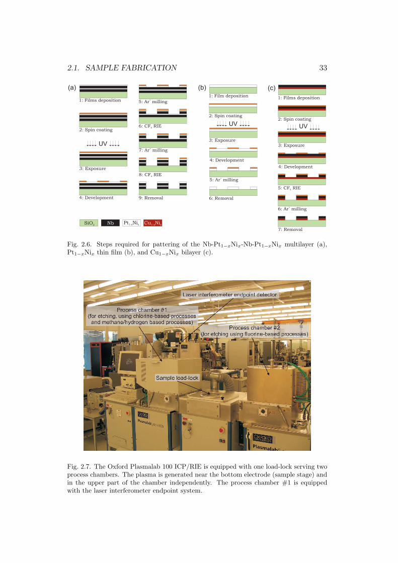
2.1. SAMPLE FABRICATION 33
Nb
UVUV
(a) (c)
1: Films deposition
2: Spin coating
3: Exposure
4: Development
5: Ar milling+
6: CF RIE4
7: Ar milling+
8: CF RIE4
9: Removal
UV
(b)
1: Film deposition
2: Spin coating
3: Exposure
4: Development
5: Ar milling+
6: Removal
1: Films deposition
2: Spin coating
3: Exposure
4: Development
5: CF RIE4
6: Ar milling+
7: Removal
SiO2Pt Ni1-x x Cu Ni1-x x
Fig. 2.6. Steps required for pattering of the Nb-Pt1−xNix-Nb-Pt1−xNix multilayer (a),Pt1−xNix thin film (b), and Cu1−xNix bilayer (c).
Fig. 2.7. The Oxford Plasmalab 100 ICP/RIE is equipped with one load-lock serving twoprocess chambers. The plasma is generated near the bottom electrode (sample stage) andin the upper part of the chamber independently. The process chamber #1 is equippedwith the laser interferometer endpoint system.

34 CHAPTER 2. EXPERIMENTAL METHODS
be impossible to remove afterwards. For this reason, the etching of Nb layerswas done in the Inductively Coupled Plasma/Reactive Ion Etcher (ICP/RIE)with a process gas of tetrafluoromethane (CF4) mixed with oxygen in pro-portion 20 to 1 (60 to 3 sccm).
In this system, the plasma is generated near the bottom electrode and inthe upper part of the chamber independently. The RF power applied to thebottom electrode is capacitively coupled, and offset by self generated DC-bias. The RF power applied to the water-cooled antenna, winded around theceramic part of the chamber, couples to the plasma inductively. The verticalelectric field near the bottom electrode provides directionality for anisotropicetching. The RF power of 100 W was applied to the antenna and 55 W wasapplied to the sample stage (bottom electrode). Fig. 2.7 shows the ICP/RIEOxford Plasmalab System 100.
The CF4 ICP/RIE combines physical etching (milling) by F+ and chem-ical etching by chemical reaction with F atoms. In CF4 plasma, F atoms areformed by electron impact dissociation of CF4. The combination of physi-cal etching with chemical provides high anisotropy (contribution of physicaletching) and high etching rate (contribution of chemical etching). The chem-ical etching also provides high material selectivity of the etching process. Theetching was done over 5 and 7 min for lower and upper layer of Nb respec-tively with the process pressure of 80 mtorr. The process chamber is equippedwith the laser interferometer endpoint detector. It can work in two modes,either in the “reflectance mode” or in the “interferometric mode”. In the“reflectance mode”, one can measure the intensity changes of light reflectedfrom the sample surface during etching. In the “interferometric mode”, theinterference signal formed by two signals from two interfaces (e.g. the top of atransparent layer and its bottom) is monitored. The system is also equippedwith CCD camera allowing accurate laser beam positioning. During the etch-ing of Nb, the “reflectance mode” was used. Since the intensity of reflectedlight from Nb is different from light reflected from Pt1−xNix and SiO2, theetching can be precisely stopped when Nb is etched away completely. Thisprevents undesired additional undercut of Nb layer.
Finally, after all layers were etched, the unexposed photoresist was re-moved in acetone. In case of hard baking of photoresist, the ultrasonic bathwas used over 5 min. Then the sample was cleaned in oxygen plasma over 1min with the RF power of 100 W. Six electrodes with the width ∼ 6µm weremade on each chip [see Figs. 2.8(a) and 2.8(b)].
To do magnetic characterization of Pt1−xNix alloys, test Pt1−xNix single-layers were pattered using photolithography and Ar ion milling [see Fig. 2.6(b)]over 20-25 min to form a bridge with both Hall and longitudinal contacts, asshown in Fig. 2.8(c).
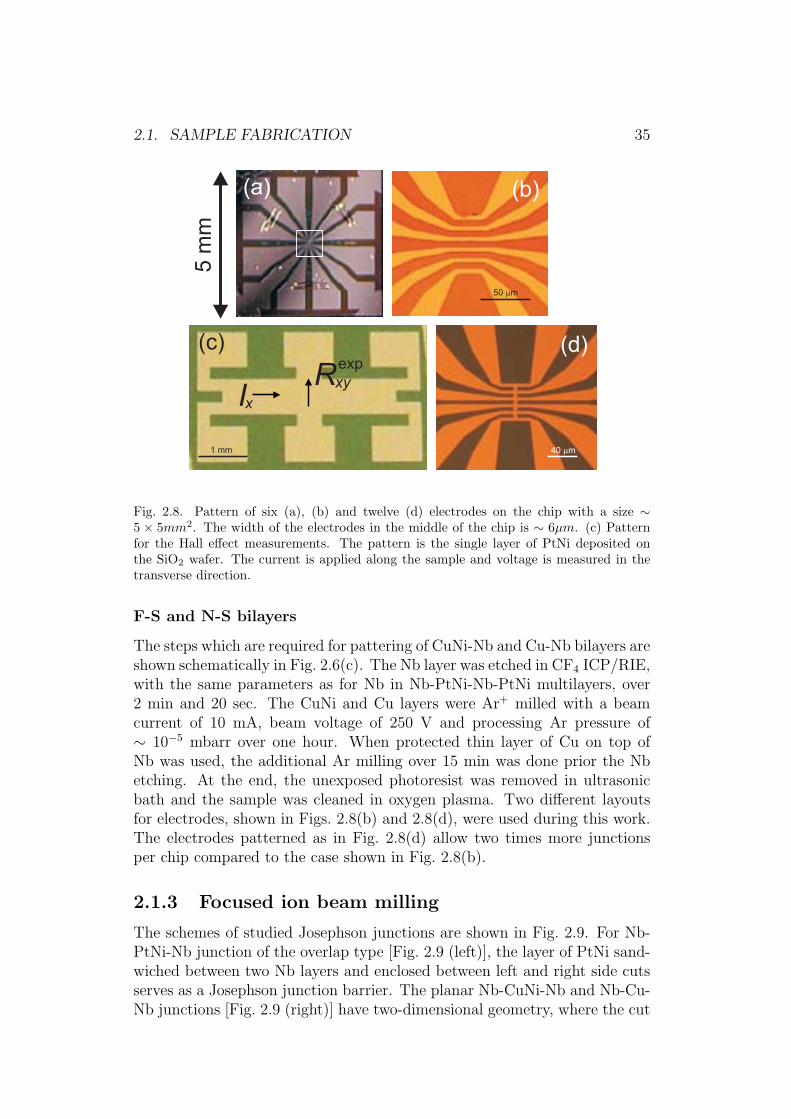
2.1. SAMPLE FABRICATION 35
5m
m(a)
50 m
(b)
IxRxy
exp
(c) (d)
40 m1 mm
Fig. 2.8. Pattern of six (a), (b) and twelve (d) electrodes on the chip with a size ∼5 × 5mm2. The width of the electrodes in the middle of the chip is ∼ 6µm. (c) Patternfor the Hall effect measurements. The pattern is the single layer of PtNi deposited onthe SiO2 wafer. The current is applied along the sample and voltage is measured in thetransverse direction.
F-S and N-S bilayers
The steps which are required for pattering of CuNi-Nb and Cu-Nb bilayers areshown schematically in Fig. 2.6(c). The Nb layer was etched in CF4 ICP/RIE,with the same parameters as for Nb in Nb-PtNi-Nb-PtNi multilayers, over2 min and 20 sec. The CuNi and Cu layers were Ar+ milled with a beamcurrent of 10 mA, beam voltage of 250 V and processing Ar pressure of∼ 10−5 mbarr over one hour. When protected thin layer of Cu on top ofNb was used, the additional Ar milling over 15 min was done prior the Nbetching. At the end, the unexposed photoresist was removed in ultrasonicbath and the sample was cleaned in oxygen plasma. Two different layoutsfor electrodes, shown in Figs. 2.8(b) and 2.8(d), were used during this work.The electrodes patterned as in Fig. 2.8(d) allow two times more junctionsper chip compared to the case shown in Fig. 2.8(b).
2.1.3 Focused ion beam milling
The schemes of studied Josephson junctions are shown in Fig. 2.9. For Nb-PtNi-Nb junction of the overlap type [Fig. 2.9 (left)], the layer of PtNi sand-wiched between two Nb layers and enclosed between left and right side cutsserves as a Josephson junction barrier. The planar Nb-CuNi-Nb and Nb-Cu-Nb junctions [Fig. 2.9 (right)] have two-dimensional geometry, where the cut

36 CHAPTER 2. EXPERIMENTAL METHODS
Nb 0Nb
NbPt Ni
1-x x
Si/SiO2
Cu Ni1-x x
Fig. 2.9. Schematic pictures of the Nb-Pt1−xNix-Nb junction of the overlap type (left)and the planar Nb-Cu1−xNix-Nb junction (right). The arrow at the planar junction lineindicates the magnetic flux and is referred to subsection 3.3.6.
Fig. 2.10. The main panel shows the FEI Nova 200 Dual Beam system. The electron gunis pointed normal to the sample surface while ion gun is tilted over 52 from electron gun.The system is equipped with one GIS for deposition of Pt. The inset shows the scheme oftypical dual beam system with one GIS. The main components of ion column are liquidGa ion source, cathode to extract the ions from the source, and the number of aperturesand magnetic lenses to shape the ions into the beam.

2.1. SAMPLE FABRICATION 37
through Nb layer forces the supercurrent to flow through non-superconductinglayer. The fabrication processing of Nb-PtNi-Nb, Nb-CuNi-Nb, and Nb-Cu-Nb junctions was performed in the dual beam Scanning Electron Microscope-Focused Ion Beam (SEM-FIB) workstation.
The FIB workstation is a very versatile and powerful tool for micro andnano fabrication. In a typical FIB system the focused ion beam is ejectedfrom a liquid metal ion source (Ga). The Ga+ ions are emitted and accel-erated by extractor voltage applied between liquid gallium source and cath-ode. The ions are shaped into a beam by a number of electrostatic lensesand apertures and focused onto the sample surface. The ions penetrate intothe sample and knock out the uppermost ions from the sample surface. Thescheme of the ion column is shown in the inset of Fig. 2.10. Alignment ofthe ion optics and positioning of the beam is completely computer controlledwhich facilitates easy handling. Characteristics of milling or deposition aredetermined using the built-in software so the desired pattern may have ba-sically any shape and can just be drawn as an image on a computer screen.Milling is performed by sputtering the material with the high energy (30keV) Ga+ ions. The milling rate is determined by the ion beam current.
In the FIB chamber there can also be one or several gas injection systems(GIS) that can be used either for deposition or increasing the milling rate.The inset of Fig. 2.10 shows the scheme of typical dual beam SEM-FIB work-station equipped with one GIS. The ion beam can also be used for imaging,providing the ion induced secondary electron image of the sample. The imageis produced by the electron contrast due to differences in crystallographic ori-entation, topography etc. However, imagining leads to implantation of Ga+
and milling of the sample so care has to be taken not to etch away or destroydelicate feature during viewing.
During this work the FEI Nova 200 Dual Beam system, which is the FIBsystem combined with SEM, was used. The main panel of Fig. 2.10 shows theFEI Nova 200 system at AlbaNova nanofabrication laboratory. The sampleis loaded directly into the vacuum chamber via the side door. The systemis equipped with one GIS for deposition of Pt. There are two detectors inthis system, namely through-the-lens detector (TLD) and Everhart Thornelydetector (ETD). The TLD uses secondary and backscatter electrons (SEand BE). It is mounted within the lens and therefore collects electrons fromimmediately over the scanned area of the sample. The ETD is mountedin the chamber above and to one side of the sample. It uses SE and BEgenerated for collection outside of the lens. The ETD has worse resolutionbut can provide better topography imaging. In additional, there is the CCDcamera installed inside the chamber. The working pressure for SEM is ∼10−5 mbar and for FIB is ∼ 10−6 mbar. The ion beam current in this systemcan be changed in steps from 1 pA to 20 nA by using a number of differentapertures. Depending on the ion beam current, the milling spot size rangingfrom 6 nm to 150 nm. The ion and electron guns are tilted with respect to

38 CHAPTER 2. EXPERIMENTAL METHODS
Fig. 2.11. Left: Position of the sample holder for narrowing of electrode. The sample ismounted on the side of the 45 wedge holder. In the right corner is the tilted FIB columnand next to the left is the vertical SEM column. The picture is taken by the CCD camerainside the chamber. The ion beam is normal to the sample surface at the sample stage tiltof 7. Right: Position of the sample holder for making the side cuts into the electrode.The sample stage is rotated over 180 in respect to the position shown in the left paneland tilted to the same angle of 7. At this position the ion beam is parallel to the samplesurface
each other at the angle of 52. The FIB-SEM allows the SEM to performimaging and the FIB to perform milling simultaneously or sequentially. Thusthe sample can be imaged during preparation without any damage. For theFEI Nova 200, the sample stage can be tilted from −10 to 59. Rotation of±180 about an axis normal to the sample stage is also possible.
3D FIB nano-sculpturing of S-F-S overlap Josephson junctions
For 3D FIB nano-sculpturing the custom-built 45 wedge holder was used,similar to that in Ref. [84]. The ion beam is perpendicular to the samplesurface when the sample stage is tilted over 7 as it shown in the left panel ofFig. 2.11. The ion beam becomes parallel to the sample surface by rotatingthe sample stage over 180 and tilting over 7 (see the right panel of Fig. 2.11).
Both pictures shown in Fig. 2.11 are taken by the CCD camera insidethe chamber. In the right corner, of both of these pictures, is the tilted FIBcolumn and next to the left is the vertical SEM column. The sample wasglued on one of the side of the 45 wedge holder by a silver paint and thenthe electrodes were grounded to the holder either by silver paint or wedgebonded using aluminium or gold wires.
The sculpturing of the junction was performed in the following sequence.First, the electrodes were narrowed from ∼ 6µm to ∼ 0.5µm with the FIBcurrent of 100 pA (milling spot size ∼ 20 nm), accelerating voltage 30 kVand with the position of ion beam perpendicular to the sample surface. The
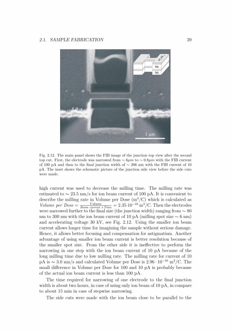
2.1. SAMPLE FABRICATION 39
Nb
PtN
ix
1-x
Nb
Fig. 2.12. The main panel shows the FIB image of the junction top view after the secondtop cut. First, the electrode was narrowed from ∼ 6µm to ∼ 0.8µm with the FIB currentof 100 pA and then to the final junction width of ∼ 206 nm with the FIB current of 10pA. The inset shows the schematic picture of the junction side view before the side cutswere made.
high current was used to decrease the milling time. The milling rate wasestimated to ∼ 23.5 nm/s for ion beam current of 100 pA. It is convenient todescribe the milling rate in Volume per Dose (m3/C) which is calculated asVolume per Dose = V olume
Beam current ×Time= 2.35·10−10 m3/C. Then the electrodes
were narrowed further to the final size (the junction width) ranging from∼ 80nm to 300 nm with the ion beam current of 10 pA (milling spot size ∼ 6 nm)and accelerating voltage 30 kV, see Fig. 2.12. Using the smaller ion beamcurrent allows longer time for imagining the sample without serious damage.Hence, it allows better focusing and compensation for astigmatism. Anotheradvantage of using smaller ion beam current is better resolution because ofthe smaller spot size. From the other side it is ineffective to perform thenarrowing in one step with the ion beam current of 10 pA because of thelong milling time due to low milling rate. The milling rate for current of 10pA is ∼ 3.0 nm/s and calculated Volume per Dose is 2.96 · 10−10 m3/C. Thesmall difference in Volume per Dose for 100 and 10 pA is probably becauseof the actual ion beam current is less than 100 pA.
The time required for narrowing of one electrode to the final junctionwidth is about two hours, in case of using only ion beam of 10 pA, in compareto about 15 min in case of stepwise narrowing.
The side cuts were made with the ion beam close to be parallel to the

40 CHAPTER 2. EXPERIMENTAL METHODS
PtNi
Fig. 2.13. SEM image of the junction side view after the side cuts were made. The junctionhas the length ∼ 230 nm. The left and right cuts are overmilled into the upper and lowerNb layers respectively for ∼ 50 nm and left side cut into SiO2/Si for ∼ 100 nm. The layerof PtxNi1−x sandwiched between two Nb layers and enclosed between left and right sidecuts serves as a Josephson junction barrier.
sample surface with the ion beam current of 10 pA. The distance betweentwo side cuts, which determine the junction length, varied from ∼ 70 nm to1500 nm for different junctions.
Figure 2.13 shows the SEM image of the junction side view with thedistance between two side cuts ∼ 230 nm. Figure 2.14 shows the SEM topimage of the same junction as it is shown in Fig. 2.13. The junction has thewidth ∼ 160 nm.
The small undercut of the bottom Nb layer may appear since the ionbeam is not perfectly parallel to the sample surface. In order to avoid suchundercuts the side cut must overmill into the upper Nb layer by the valuewhich depends on the actual alignment of the ion beam and the junctionwidth. The minimum overmill distance is given by a = tanα · b, where bis a junction width and α is an angle between ion beam and normal to thejunction side. The left and right cuts of the Junction shown in Fig. 2.13are overmilled into the upper and lower Nb layers respectively for ∼ 50 nm.The left side cut is also overmilled into SiO2/Si for ∼ 100 nm. The effect ofundercut of the Nb layer and the way how to get rid of it will be discussedin subsection 3.3.3.
Figure 2.15 shows the SEM image of typical chip, ready for measurements,

2.1. SAMPLE FABRICATION 41
Fig. 2.14. SEM image of the junction top view after the side cuts were made. The junctionis the same as it is shown in Fig. 2.13. The width of the junction is ∼ 160 nm.
where the junction is made in the middle of each electrode. In total, there aresix junctions made on one chip. Therefore junctions with the same propertiescan be made with different geometries.
FIB fabrication of planar S-F-S and S-N-S Josephson junctions
The chip with patterned electrodes was fixed on a standard SEM stub bysilver paint or carbon tape and bonded to the stub for a good electricalgrounding. After focusing and correcting the astigmatism, a single cut ofthe length 6 µm through the top Nb layer was made at the beam currentof 1 or 10 pA. The ion beam was always normal to the sample surface andhad a dwell time of 0.3 µs, a beam spot overlap of 20 %, and an accelerationvoltage of 30 kV through the process. The depth of the cut was controlledby changing the etching time. The length of the junction was varied from 4to 6 µm.
The advantage of using small current of 1 pA is smaller width of thecut which is determined by the beam spot size (< 6 nm). However, thesmaller current requires longer milling time. Typical time is about 1 to2 min depending on the depth of the cut. During this time, the drift ofthe ion beam can be quite substantial, leading to a non-uniform milling andincreasing the final junction width. Instead, 10 pA ion current requires muchshorter time (∼ 5 sec) during which the drift is not crucial. After the cut
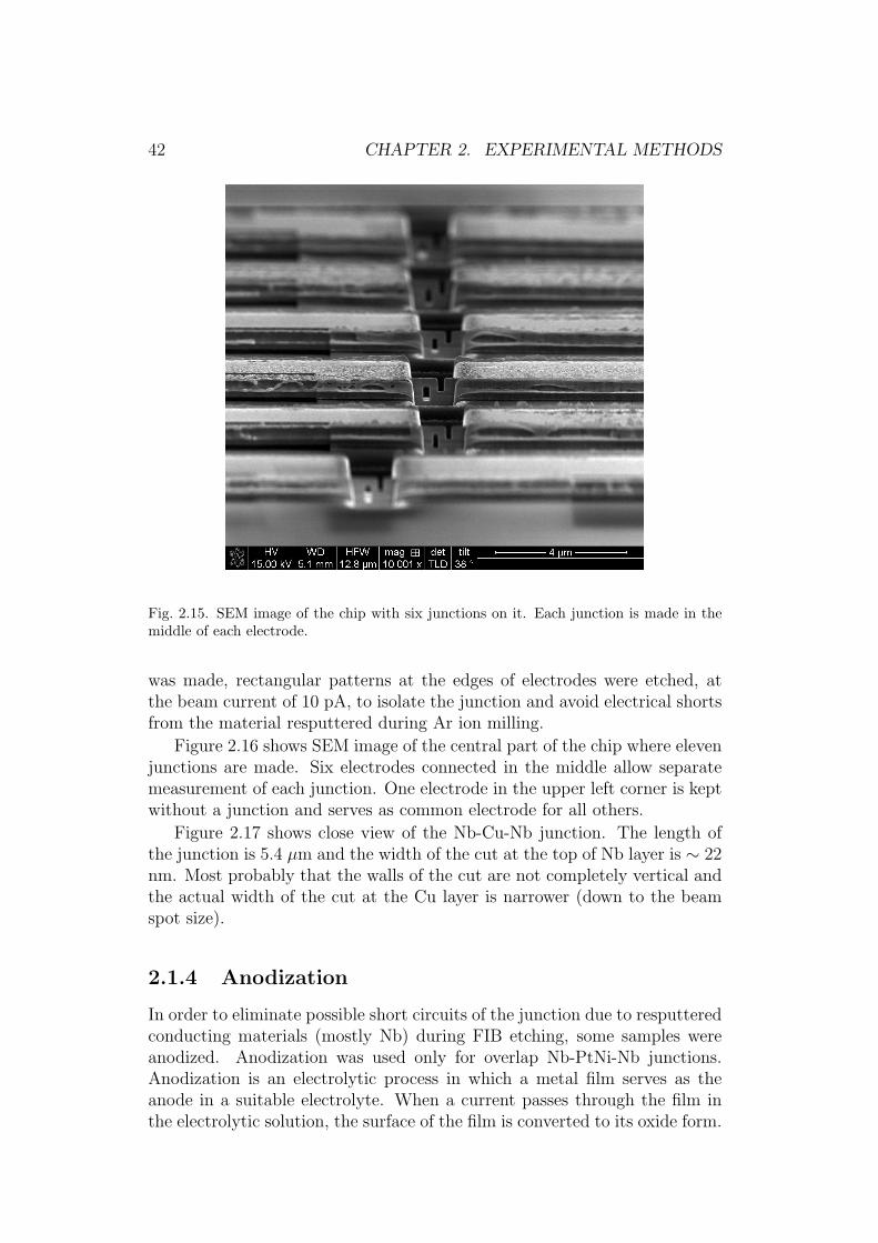
42 CHAPTER 2. EXPERIMENTAL METHODS
Fig. 2.15. SEM image of the chip with six junctions on it. Each junction is made in themiddle of each electrode.
was made, rectangular patterns at the edges of electrodes were etched, atthe beam current of 10 pA, to isolate the junction and avoid electrical shortsfrom the material resputtered during Ar ion milling.
Figure 2.16 shows SEM image of the central part of the chip where elevenjunctions are made. Six electrodes connected in the middle allow separatemeasurement of each junction. One electrode in the upper left corner is keptwithout a junction and serves as common electrode for all others.
Figure 2.17 shows close view of the Nb-Cu-Nb junction. The length ofthe junction is 5.4 µm and the width of the cut at the top of Nb layer is ∼ 22nm. Most probably that the walls of the cut are not completely vertical andthe actual width of the cut at the Cu layer is narrower (down to the beamspot size).
2.1.4 Anodization
In order to eliminate possible short circuits of the junction due to resputteredconducting materials (mostly Nb) during FIB etching, some samples wereanodized. Anodization was used only for overlap Nb-PtNi-Nb junctions.Anodization is an electrolytic process in which a metal film serves as theanode in a suitable electrolyte. When a current passes through the film inthe electrolytic solution, the surface of the film is converted to its oxide form.
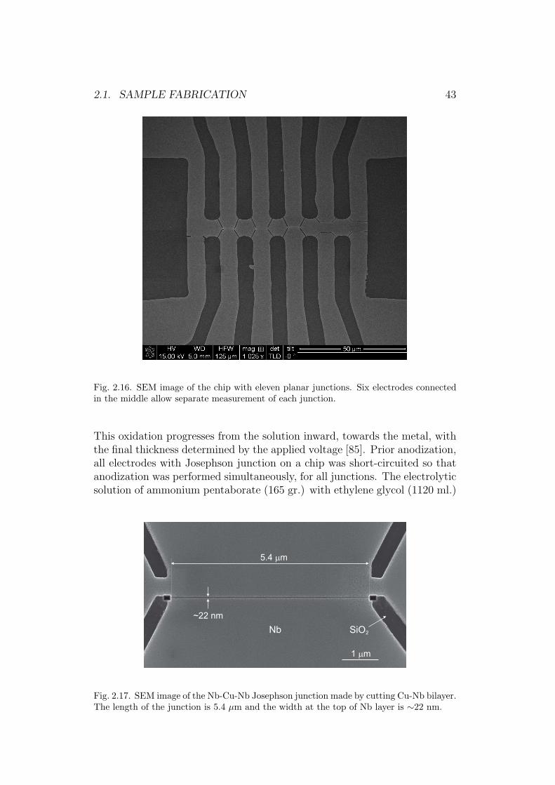
2.1. SAMPLE FABRICATION 43
Fig. 2.16. SEM image of the chip with eleven planar junctions. Six electrodes connectedin the middle allow separate measurement of each junction.
This oxidation progresses from the solution inward, towards the metal, withthe final thickness determined by the applied voltage [85]. Prior anodization,all electrodes with Josephson junction on a chip was short-circuited so thatanodization was performed simultaneously, for all junctions. The electrolyticsolution of ammonium pentaborate (165 gr.) with ethylene glycol (1120 ml.)
Nb SiO2
1 m
5.4 m
~22 nm
Fig. 2.17. SEM image of the Nb-Cu-Nb Josephson junction made by cutting Cu-Nb bilayer.The length of the junction is 5.4 µm and the width at the top of Nb layer is ∼22 nm.

44 CHAPTER 2. EXPERIMENTAL METHODS
and deionized water (760 ml.) was used.The anodization process proceeded as follows:
1. The cathode in the electrolytic solution was grounded while the sample(anode) was connected to a power supply;
2. The voltage from the power supply was ramped, from 0 V to 16 V,maintaining the initial constant current of about 10 mA through thesample. The overall ramp time was approximately 1 min;
3. The voltage was holding constant at 16 V. During the voltage holdtime, the current through the sample dropped exponentially as theoxide layer densified;
4. When the current level reached the value of about 0.2 mA, the powersupply was abruptly switched off.
The total immersion time was approximately 15 min.As it was mentioned in subsection 2.1.1, the anodization is inadmissible
in case of having the Au as contact layer. The reason for this is that theused electrolytic solution has etching influence on Au. The result of etchingof Au by electrolytic solution is destroying of junction. Figure 2.18 showsthe junction with Au on top of Nb-PtNi-Nb trilayer after anodization.
2 m
junction
Fig. 2.18. SEM image of the sample with Au as contact layer after anodization. The usedelectrolytic solution etched Au and destroyed the junction.

2.2. SAMPLE CHARACTERIZATION 45
2.2 Sample characterization
2.2.1 EDS Characterization of PtNi thin films
To characterize the Pt1−xNix thin films, the Hall effect was studied and anal-ysis of chemical composition of single-layer Pt1−xNix thin films by means ofenergy dispersive X-ray spectroscopy (EDS) was performed. The experimen-tal setup for the Hall effect measurements is roughly the same as for junctioncharacterization and will be described in the next subsection while in thissubsection EDS technique will be briefly described3.
The EDS is add-on that can be used for analytical microscopy in bothSEM and Transmission Electron Microscope (TEM). When used in TEM theresolution can nearly as good as the spot size, i.e. a couple of nm. For SEMon the other hand, the resolution is of the order of µm since the electrons canbe scattered around the volume much larger than the spot size, and X-raysgenerated can easily reach the specimen surface. In this work, the JEOLJSM-7000F system was used, which is the high resolution SEM equippedwith energy dispersive and wavelength dispersive spectrometers.
When an incident electron hits the specimen, it causes an inner shellelectron to be ejected from the specimen atom. An electron from an outershell then jumps to the inner shell. The difference in energy between theshells is sent out as an X-ray. The different X-ray peak can be observedin the EDS spectrum. The K-peak indicates that the first ejected electronoriginated to the K-shell, the L-peak means the L-shell and so on. The indicesα, β... indicate from where the second electron jumps. Since each elementhas a unique electronic structure, the series of generated X-ray photons arecharacteristic of the particular element emitting the X-rays. The intensityof the X-rays is proportional to number of atoms generating the X-rays.Note, that not only the characteristic X-rays are generated when the electronbeam hits the sample. There are also secondary electrons and backscatteredelectrons. At the surface of the sample, X-rays emission is enhanced byscattered electrons from below. Moreover, those X-rays produced at depth ofanalytical volume must pass through a certain distance within the sample andrisk being absorbed. The escape energy of an element is the energy thresholdneeded to initiate inner sphere ionization and generate characteristic X-rays.In addition to incident electrons, other X-rays can also exceed this threshold.Ionizing X-rays can be generated by ionization of other elements with higherescape energy. All these factors should be taken into account while processingthe measured data.
In SEM-based EDS system, the generated X-rays are detected by a lithiumdrifted silicon (Si(Li)) detector. When an X-ray strikes the detector, it willgenerate a photoelectron within the body of the Si. As this photoelectron
3The EDS measurements were carried out at Electron Microscopy Center, Departmentof Materials and Environmental Chemistry, Stockholm University.

46 CHAPTER 2. EXPERIMENTAL METHODS
travels through the Si, it generates electron-hole pairs (every 3.8 eV). Theelectrons and holes are attracted to opposite ends of the detector by thestrong electric field. The size of the generated current pulse depends on thenumber of electron-hole pairs created, which in turn depends on the energyof the incoming X-ray. The pulses are then stored in a multichannel ana-lyzer where each channel represents a certain amplitude interval of the pulses.Thus, an X-ray spectrum can be acquired giving information on the elementalcomposition of the material under examination. In a spectrum, the exponen-tially decreasing energy known as the Bremsstrahlug can be seen. This isbackground X-rays produced by inelastic scattering (loss of energy) of theprimary electron beam in the specimen. It covers a range of energies up tothe energy of the electron beam. For SEM analysis, this is the backgroundin the spectrum above which the characteristic peaks from the elements rise.
Electron probe microanalysis has traditionally been used as a bulk analyt-ical technique for the characterization of samples with the spatial resolution∼ 1µm. Successful utilization of the technique requires an interplay betweenthe heterogeneity of the sample, the beam energy, and the X-ray energies.Typical beam energies of 10-30 keV have excitation depth of 1-5 µm, lowerbeam energies (5-10 keV) have excitation depth of 0.1-1 µm, and ultra-lowenergies (below 5 keV) have excitation depth of 0.05-0.1 µm. However at suchlow energies, quantitative complexities arise due to fewer X-ray lines avail-able. When analyzing a thin film specimen with a thickness of the order ofhundred nanometers or less, incident electrons penetrate into the substrate.In this case, the EDS analysis becomes a complicated task. The character-istic X-ray intensity from the thin film can be influenced by the parasiticsignal from the substrate [86, 87].
2.2.2 Low-temperature measurement setup
All measurements during this work were carried out using either a liquidhelium (He) dewar (left panel in Fig. 2.19) or cryogen-free magnet system(right panel in Fig. 2.19) with a flowing gas insert.
The sample was glued on the plug-in by a silver paint and then wedgebonded using aluminium or gold wires [see Fig. 2.20(a)]. possible to doa four point measurement of all six junctions in one cooling cycle. Theplug-in was mounted on the probe and then fixed in the gas flow insert.In case of using the dewar, the gas flow insert was cooled in 4He dewarunder continuous pumping. In such a refrigerator a small fraction of theliquid 4He from the main bath flows through a suitable flow impedance intothe insert. The sample is located in the vapour above the liquid 4He. Thecontinuous pumping of the 4He vapour allows to reach the temperature about1.6 K. In this case, the 4He is pumped away to the atmosphere. Whenthe dewar was used the superconducting solenoid mounted on the insert orbuilt-in superconducting magnet was used for magnetic field measurements.
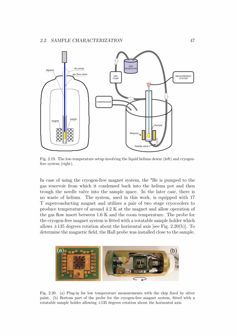
2.2. SAMPLE CHARACTERIZATION 47
sample
dipstick
magnet
gas flow insert
dry pumpGAS
RESERVOIR
DRY
PUMP
COMPRESSOR
MEASUREMENT
SYSTEM
Magnet
Sample
Needle valve
Fig. 2.19. The low-temperature setup involving the liquid helium dewar (left) and cryogen-free system (right).
In case of using the cryogen-free magnet system, the 4He is pumped to thegas reservoir from which it condensed back into the helium pot and thentrough the needle valve into the sample space. In the later case, there isno waste of helium. The system, used in this work, is equipped with 17T superconducting magnet and utilizes a pair of two stage cryocoolers toproduce temperature of around 4.2 K at the magnet and allow operation ofthe gas flow insert between 1.6 K and the room temperature. The probe forthe cryogen-free magnet system is fitted with a rotatable sample holder whichallows ±135 degrees rotation about the horizontal axis [see Fig. 2.20(b)]. Todetermine the magnetic field, the Hall probe was installed close to the sample.
(a) (b)
Fig. 2.20. (a) Plug-in for low temperature measurements with the chip fixed by silverpaint. (b) Bottom part of the probe for the cryogen-free magnet system, fitted with arotatable sample holder allowing ±135 degrees rotation about the horizontal axis.

48 CHAPTER 2. EXPERIMENTAL METHODS
RSER JJR
S
preamplifier
preamplifier
+ -
+ -
PXI
LabVIEW
PC
AD
CA
DC
Fig. 2.21. Diagram of the I − V measurement setup. RSER is the series resistance and RS
is the resistor used to measure the current.
For current-voltage (I−V ) measurements the four point contact methodwas used. It means that the measurement of the voltage and applying ofthe current were done at the different contacts. By using this method onlythe voltage across the junction was measured and not the voltage across thecontact resistance of the probes and oxide layer.
The measured samples were always current biased. All I − V measure-ments were performed using real-time PCI eXtensions for Instrumentation(PXI) system which is a rugged PC-based platform. The instrumentation isintegrated by means of a LabVIEW-based measurement program. An arbi-trary waveform generator was used as a current source. The sample voltagewas measured using the 24-bit analog-to-digital converter. The software-based lock-in amplifier was used to extract the resistance from I − V sig-nal. The PXI system allows simultaneous measurements of different samplesor/and measurements of the signal from the sample and e.g. the signal fromthe Hall probe. A scheme of the measurement setup is shown in Fig. 2.21.The biasing is done by connecting the series resistor, another smaller re-sistor (100Ω) is used in order to read out the current flowing through thecircuit by measuring the voltage. Both current (indirectly) and voltage ismeasured by using battery driven differential preamplifiers. Simultaneously,the Hall probe is current biased and the voltage signal is used to calculatethe magnetic field at the sample.

Chapter 3
Results and discussion
3.1 Chemical composition of PtNi thin films
The study of chemical composition of thin films by EDS is not an easy taskas it seems to be at the first sigh. The reason for this is the presence ofa thick substrate material underneath analyzed thin film and a small filmthickness in comparison to the whole analytical volume.
The typical spectra for 5 keV and 15 keV electron beam voltages areshown in Fig. 3.1 and Fig. 3.2, respectively. The letters indicate the peakswhich are used for determination of Ni, Pt, Si and O concentrations. Thespectra were taken from a film with a thickness of 50 nm which was depositedfrom a Pt/Ni target with a relative Ni area of 44.4 %. The incident elec-tron beam in this case was normal to the surface. To analyze the measuredspectra, first the background is removed and then the integrated peak inten-sity is determined from each elemental peak in the sample. This value fromthe sample is then normalized to known standard values for each element.The treatment of the measured X-ray spectra is usually done using a specialsoftware. In this work, INCA software was used. This software takes intoaccount the so-called matrix effect, i.e. the combined effect of all componentsof the sample other than the desired on the measurement result. These ef-fects will be different for different accelerating voltages, and correspondinglyfor different analytical volumes. Thus, it is important to know exactly thesize and shape of the analytical volume. The extended algorithm of Pouchouand Pichoir (XPP) [88] is used to make the corrections for the effect on
• the electron interaction (depth of electron penetration and fraction ofbackscattered electrons) with the sample (atomic number correction);
• the absorption of the emitted X-rays in the sample which reduces themeasured intensity;
• the fluorescence of secondary X-rays which increases the measured in-tensity.
49

50 CHAPTER 3. RESULTS AND DISCUSSION
Pt
Ni L
O
Ni L
C
Si
0 1 2 3 4 keV
Fig. 3.1. X-ray energy spectrum of the PtNi thin film which was deposited from a targetwith a relative Ni area of 44.4 % for an incident electron beam energy of 5 keV. Thepeaks which are used for determination of Ni, Pt, Si and O concentrations are markedrespectively. The arrow indicates the possible Si induced secondary fluorescence of Ni.
The silicon and oxygen signals on the spectra shown in Fig. 3.1 andFig. 3.2 are coming from the oxidized Si wafer, while the carbon signal is dueto contamination in the SEM. The Si peak becomes much stronger for 15keV electron beam. In this case, the interaction volume is mostly confined
Si
O
Pt
Ni K Ni K
0 5 10 keV
Fig. 3.2. X-ray energy spectrum of the PtNi thin film which was deposited from a targetwith a relative Ni area of 44.4 % for an incident electron beam energy of 15 keV. Thepeaks which are used for determination of Ni, Pt, Si and O concentrations are markedrespectively.

3.1. CHEMICAL COMPOSITION OF PtNi THIN FILMS 51
0 15 30 45 60 750
15
30
45
60
75
(a)
Ni c
once
ntra
tion
(at.%
)
Ni target area (%)
electron beam energy: 5 keV 10 keV 15 keV 30 keV
0 15 30 45 60 750
15
30
45
60
75
(b)
Ni c
once
ntra
tion
(at.%
)
Ni target area (%)
electrone beam energy:(including effect of C, O and Si)
5 keV 10 keV 15 keV 30 keV
Fig. 3.3. Ni concentrations of the PtNi thin films determined by EDS as a function of therelative Ni target area for different electron beam energies. (a) the sample is considered asbulk PtNi alloy and (b) the sample is considered as mixture of PtNi alloy with C, O andSi. The dashed lines represent linear fit to Ni concentrations at different electron beamenergies with double weight of concentration for 5 keV and triple for 15 and 30 keV.
in the Si wafer. From Fig. 3.1, the Si induced fluorescence effect (indicatedby the arrow) can be seen. In this case, the Ni Lα (0.85 keV) and Ni Lβ
(0.87 keV) peaks are used to estimate the Ni concentration. For an electronbeam energy of 15 keV (Fig. 3.2), the Si induced fluorescence effect can beneglected since the Ni Kα (7.48 keV) and Ni Kβ (8.26 keV) peaks are usedfor the determination of the Ni concentration.
Figure 3.3 shows the dependence of the Ni concentration of PtNi thinfilms on the relative Ni target area. The thicknesses of the PtNi thin filmsare ranging from 50 to 60 nm. The error in the relative Ni target area wastaken to be ∼ 5 %. There are two sources for this error. First, the exact sizeof the Ni segment can slightly vary between different segments, and second,the erosion track of the target is not well defined so there can be an error inthe track diameter. Both the Ni segment size and the erosion track diameterwere used in the determination of the relative Ni target area (see subsection2.1.1).
Since the quantitative analysis routine, XPP, assumes the material underexamination to be a uniform alloy rather than a layered structure (Pt1−xNixalloy on Si/SiO2 wafer), two different cases were considered. First, it wasassumed that the sample is only a Pt1−xNix alloy [Fig. 3.3(a)], and second,the sample was considered to be the mixture of a Pt1−xNix alloy with C,O and Si [Fig. 3.3(b)]. From comparison of Figs. 3.3(a) and 3.3(b) it isseen that the difference between the two cases is rather small. It is seenthat the measured Ni concentration is proportional to the relative Ni targetarea, however, EDS measurements at different electron beam energies provideslightly different estimation of Ni concentrations. This difference can be dueto the following reasons:

52 CHAPTER 3. RESULTS AND DISCUSSION
• effect of the substrate which can provoke error in the correction ofsecondary fluorescence by Si;
• change in the yield of backscattered electrons in the film due to thefilm/substrate interface;
• secondary fluorescence of Ni by Pt in the film.
All these factors will give the rise to the error in XPP correction.
A possible reason for different Ni concentrations depending on electronbeam energies is the error in fluorescence correction. The fluorescence effectof Si is expected to be less in the case of the PtNi alloy on a Si/SiO2 sub-strate in comparison to the bulk Pt/Ni/Si/SiO2 alloy. In case of the PtNialloy on Si/SiO2 the amount of X-rays which can cause secondary fluores-cence is less due to energy loss at the film/substrate interface. For higherelectron beam energies the Si induced fluorescence can be neglected whilethe error in fluorescence correction can be important for lower beam ener-gies. On the other hand, the change in Ni concentration is rather small whenwe ignore the presence of Si/SiO2 at all [see Figs. 3.3(a) and 3.3(b)]. This im-plies that the difference in measured Ni concentrations for differentelectron beam energies can be only partly explained by the errorin correction of Si induced secondary fluorescence.
The determination of the composition from the characteristic X-rays canonly be made correctly if it is exactly known where the X-rays are beingproduced. The generation of X-rays as a function of depth z is representedby the X-ray depth distribution function ϕ(ρz), where ρ is the density ofa sample material. This function describes the volume and shape of theanalytical volume [86]. The shape of the ϕ(ρz) curve for the thin film isdifferent from that for the bulk standard since the scattering of incidentelectrons at the film/substrate interface is different from the scattering inthe bulk specimen. The backscattered electron yield at the film/substrateinterface increases with the atomic number of the substrate. Therefore, theX-ray production in the film increases [89].
At a beam energy of 5 keV, most of the analytical volume is confinedin the film and not in the substrate. This can be seen in Fig. 3.1 wherethe amount of Ni and Pt is larger than the amount of Si and O. Due tothe low energy of incident electrons there will be a lack of electrons at thefilm/substrate interface, and consequently a lack of backscattering electrons.Thus the effect of backscattering electrons will be less seen for beam energyof 5 keV.
For electron beam energies of 15 keV and higher, the analytical volume isconfined much deeper in the Si substrate as it can be seen from Fig. 3.2 wherethe amount of Si is larger than all other elements. In this case the proba-bility for high energy incident electrons to be reflected at the film/substrate

3.1. CHEMICAL COMPOSITION OF PtNi THIN FILMS 53
interface is quite small. Moreover, the probability to be excited by backscat-tering electrons is higher for less energetic Pt M lines than for high energeticNi K lines. Those two types of lines are used to estimate the Ni and Ptconcentrations for electron beam energies of 15 and 30 keV.
However, at intermediate electron beam energies such as 10 keV, the an-alytical volume is enough confined within the PtNi thin film. There is aconsiderable amount of backscattering electrons from the film/substrate in-terface with high enough energy. In this case the probability to overestimatethe value of the concentration is higher for Ni since less energetic L lines areused for quantitative analysis.
From the discussion above the following conclusions can be made. Forvery low electron beam energies, the effect of the backscattering electronsfrom the film/substrate interface is small simply due to lack of these elec-trons. At high electron beam energies, this effect is also small and has moreinfluence on the Pt concentration leading to a slightly overestimated Pt con-centration. However, for an electron beam energy of about 10 keV, theeffect of backscattering electrons from the film/substrate interfaceis substantial and can lead to an overestimated Ni concentration.
In order to further investigate the effect of the substrate on actual Niconcentrations, the dependence of the Ni concentration on the angle of inci-dence of the electron beam was studied. Figure 3.4 shows the dependence ofNi, Pt, Si and O concentrations on the deviation angle from the normal tothe surface for a thin film deposited from the target covered by 44.4 % of Ni.The results are presented for the electron beam energies of 5 keV [Fig. 3.4(a)]and 15 keV [Fig. 3.4(b)]. The Ni concentration remains almost the same fordifferent angles and for different beam energies while the Pt concentration isnot constant for the electron beam energy of 5 keV. The contents of Si andO vary with the electron beam incident angle for both beam energies. Theincrease of oxygen contents and decrease of Si with increasing the angle isexpected since the interaction volume will be now confined more in the SiO2
layer than in Si. The increase of oxygen is not proportional to the decreaseof Si for the electron beam energy of 5 keV. In this case, the Pt concentrationdecreases while the Ni concentration remains the same. Since the PtNi alloyis expected to be homogeneous, the Pt and Ni concentrations should followthe same trend. In order to understand whether this difference is due to anerror in the correction procedure or caused by a change in the angle, thearea of elemental peaks from the spectrum as a function of electron beamincident angle is plotted in Fig. 3.5. Here the same spectrum was used as inFig. 3.4 but no correction was made to the data. The correction is neededto get concentrations in the at.%.
The concentrations of Pt, Ni and O increase with increasing the angle,while the Si content has the trend to decrease for electron beam energiesof 5 keV. This behavior is plausible since, as it was mentioned above, uponincreasing the angle, the interaction volume is confined more in PtNi/SiO2
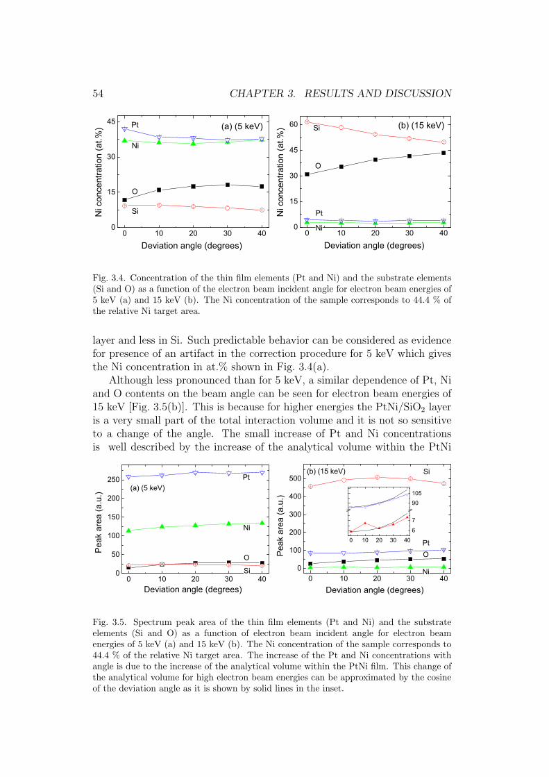
54 CHAPTER 3. RESULTS AND DISCUSSION
0 10 20 30 400
15
30
45
(a) (5 keV)
Pt
Ni
Si
O
Ni c
once
ntra
tion
(at.%
)
Deviation angle (degrees)
0 10 20 30 400
15
30
45
60
(b) (15 keV)
Pt
Ni
O
Si
Ni c
once
ntra
tion
(at.%
)
Deviation angle (degrees)
Fig. 3.4. Concentration of the thin film elements (Pt and Ni) and the substrate elements(Si and O) as a function of the electron beam incident angle for electron beam energies of5 keV (a) and 15 keV (b). The Ni concentration of the sample corresponds to 44.4 % ofthe relative Ni target area.
layer and less in Si. Such predictable behavior can be considered as evidencefor presence of an artifact in the correction procedure for 5 keV which givesthe Ni concentration in at.% shown in Fig. 3.4(a).
Although less pronounced than for 5 keV, a similar dependence of Pt, Niand O contents on the beam angle can be seen for electron beam energies of15 keV [Fig. 3.5(b)]. This is because for higher energies the PtNi/SiO2 layeris a very small part of the total interaction volume and it is not so sensitiveto a change of the angle. The small increase of Pt and Ni concentrationsis well described by the increase of the analytical volume within the PtNi
0 10 20 30 400
50
100
150
200
250
Si
O
Ni
Pt(a) (5 keV)
Pea
k ar
ea (a
.u.)
Deviation angle (degrees)
0 10 20 30 400
100
200
300
400
500Si
O
Ni
Pt
(b) (15 keV)
Pea
k ar
ea (a
.u.)
Deviation angle (degrees)
0 10 20 30 40
6
7
90105
Fig. 3.5. Spectrum peak area of the thin film elements (Pt and Ni) and the substrateelements (Si and O) as a function of electron beam incident angle for electron beamenergies of 5 keV (a) and 15 keV (b). The Ni concentration of the sample corresponds to44.4 % of the relative Ni target area. The increase of the Pt and Ni concentrations withangle is due to the increase of the analytical volume within the PtNi film. This change ofthe analytical volume for high electron beam energies can be approximated by the cosineof the deviation angle as it is shown by solid lines in the inset.
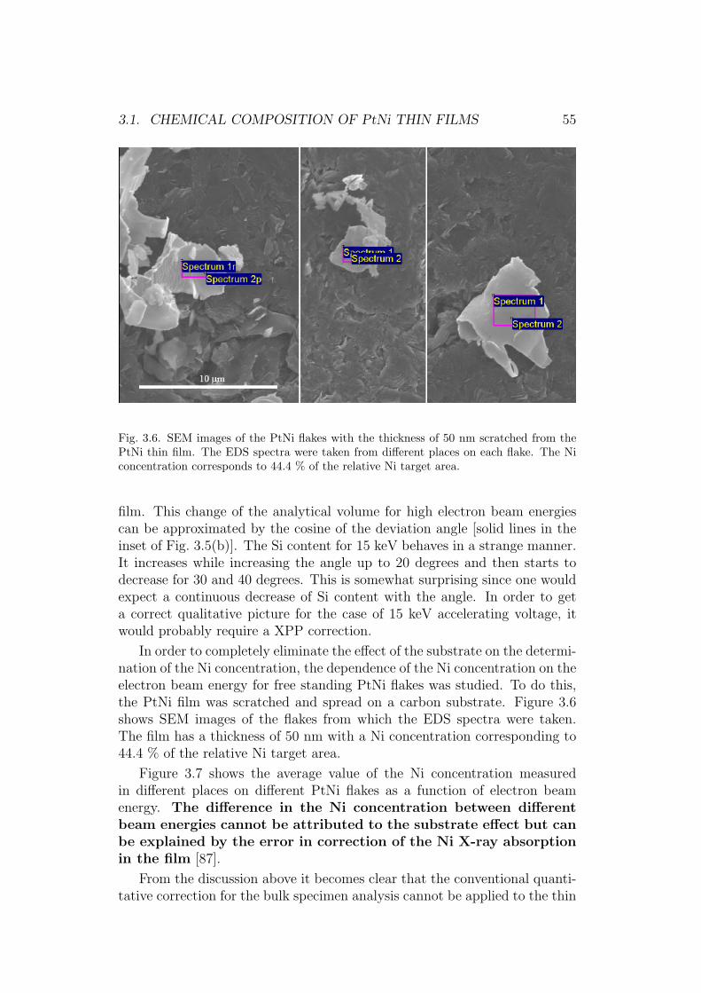
3.1. CHEMICAL COMPOSITION OF PtNi THIN FILMS 55
Fig. 3.6. SEM images of the PtNi flakes with the thickness of 50 nm scratched from thePtNi thin film. The EDS spectra were taken from different places on each flake. The Niconcentration corresponds to 44.4 % of the relative Ni target area.
film. This change of the analytical volume for high electron beam energiescan be approximated by the cosine of the deviation angle [solid lines in theinset of Fig. 3.5(b)]. The Si content for 15 keV behaves in a strange manner.It increases while increasing the angle up to 20 degrees and then starts todecrease for 30 and 40 degrees. This is somewhat surprising since one wouldexpect a continuous decrease of Si content with the angle. In order to geta correct qualitative picture for the case of 15 keV accelerating voltage, itwould probably require a XPP correction.
In order to completely eliminate the effect of the substrate on the determi-nation of the Ni concentration, the dependence of the Ni concentration on theelectron beam energy for free standing PtNi flakes was studied. To do this,the PtNi film was scratched and spread on a carbon substrate. Figure 3.6shows SEM images of the flakes from which the EDS spectra were taken.The film has a thickness of 50 nm with a Ni concentration corresponding to44.4 % of the relative Ni target area.
Figure 3.7 shows the average value of the Ni concentration measuredin different places on different PtNi flakes as a function of electron beamenergy. The difference in the Ni concentration between differentbeam energies cannot be attributed to the substrate effect but canbe explained by the error in correction of the Ni X-ray absorptionin the film [87].
From the discussion above it becomes clear that the conventional quanti-tative correction for the bulk specimen analysis cannot be applied to the thin

56 CHAPTER 3. RESULTS AND DISCUSSION
5 10 15 20
38
40
42
44
46
48
50
Electron beam energy (keV)
Ni c
once
ntra
tion
(at.%
)
Ni target area = 44.4 %
Fig. 3.7. The EDS measured average value of the Ni concentration of the PtNi flakes asa function of electron beam energy. The PtNi flakes were scratched from the film with aNi concentration corresponding to 44.4 % of the relative Ni target area and are shown inFig. 3.6.
film when using low electron beam energies. The XPP correction procedureseems to work properly for electron beam energies of 15 and 30 keV. For elec-tron beam energies above 10 keV one can neglect the Si induced secondaryfluorescence effect. For an electron beam energy of 10 keV, the effect ofbackscattering electrons from the film/substrate interface is substantial andcan lead to an overestimated Ni concentration. The absorption probabilityof the light Ni L series, which is used for the determination of the Ni con-centration in case of low beam energies, is much higher than the absorptionprobability of the high energy Ni K series. In general, the absorption is verydifficult to correct when working with light elements. The error in the X-rayabsorption correction is smaller at higher beam energies. It is also difficultto correctly compensate for the secondary fluorescence of the very light NiL series by Pt in case of a low electron beam energy. In what follows, Niconcentrations are obtained from the linear fit to the EDS data at electronbeam energies of 5, 10, 15 and 30 keV but with two times larger weight for5 keV and three times for 15 and 30 keV [dashed line in Fig. 3.3(b)].
3.2 Magnetic properties of PtNi thin films
This section summarizes the main results presented in the appended paperVI and also includes some unpublished results.
PtNi thin films with the thicknesses of 50-60 nm and Ni concentrations

3.2. MAGNETIC PROPERTIES OF PtNi THIN FILMS 57
0 40 80 120 160 200 240 2800.000
0.004
0.008
0.012
0.016
R* xy
/ H
( /
T)
T (K)
13 at.% 27 at.% 40 at.%
0.00
0.02
0.04
0.06
0.08
67 at.%
Fig. 3.8. Field normalized Hall resistance as a function of temperature for Ni concen-trations of 13 (open squares, left axis), 27 (solid circles, left axis), 40 (open stars, leftaxis) and 67 (open circles, right axis) at.%. The data are obtained from the transverseresistances by subtracting the linear term due to longitudinal resistance.
of 13, 27, 40 and 67 % were studied. Measurements were carried out in acryogen-free magnet system over a temperature range from 1.8 K to 300 Kand fields up to ±10 T.
Figure 3.8 shows the T dependence of the Hall resistance R∗xy normalized
by the absolute value of the applied field, perpendicular to the film. Anonset of R∗
xy(T ) with decreasing temperature is seen for all studied films.The R∗
xy/|H| has a strong temperature dependence and increases rapidlywith increasing Ni concentration. At T = 2 K, R∗
xy/|H| differs by more thantwo orders of magnitude between films with the largest (67 at.%) and thesmallest (13 at.%) Ni concentrations.
3.2.1 Films with low Ni concentration
The main panels of Figs. 3.9 and 3.10 show Hall resistances Rxy as a func-tion of perpendicular magnetic field for films with 13 at.% and 27 at.% ofNi, respectively, at low temperatures. Both Rxy and R∗
xy represent the Hallresistance but they are determined in a slightly different way (see appendedpaper VI). The films in Figs. 3.9 and 3.10 show hysteresis at the lowest T(solid circles) with significant coercivity of 0.16 T and 0.6 T, respectively, in-dicating out-of-plane magnetic anisotropy. It is seen, however, that Rxy(H)does not saturate at large fields. This is due to a weak magnetism in thosestrongly diluted, sub-critical, PtNi films. In this case the saturable extraor-dinary Hall effect (EHE) is of the same order as the non-saturable ordinaryHall effect contribution [90]. With increasing temperature, the coercivity

58 CHAPTER 3. RESULTS AND DISCUSSION
-2 -1 0 1 2
-1.4
-0.7
0.0
0.7
1.4 13 at.% of Ni
Rxy
(m)
H (T)
T=1.8 K T=7 K
H
-1.5 0.0 1.5
-1.4
-0.7
0.0
0.7
1.4 T=60 K T=280 K
Rxy
(m)
H (T)
Fig. 3.9. Magnetic field dependence of the Hall resistance at low (main panel) and elevated(inset) temperatures for film with 13 at.% of Ni.
rapidly decreases and vanishes at Tb ≃ 7 K for the film with 13 at.% of Niand Tb ≃ 12.8 K for 27 at.% of Ni. However, Rxy(H) remains nonlinear,see curves with open circles in the main panel of Figs. 3.9 and 3.10, indi-cating presence of residual superparamagnetism in the films. Therefore, Tb
represents the superparamagnetic blocking temperature of the films.
The M(H) curves of superparamagnets are represented by the Langevinfunction [67] L = coth (µH/kBT )−kBT/µH, where µ is the total moment ofindividual magnetic domains or clusters. By fitting Rxy(H), measured justabove the blocking temperature, with the Langevin function one can estimatean average magnetization µ = 1.19 · 10−21 A·m2 and µ = 3.3 · 10−21 A·m2 forthe films with 13 at.% and 27 at.% of Ni, respectively. Therefore, magneticdomains of the film are composed of about 128 and 356 µB, respectively.
3.2.2 Films with high Ni concentration
PtNi films with over-critical Ni concentrations show a distinctly different be-havior compared to films with sub-critical Ni concentrations described above.
Figure 3.11 shows Rxy as a function of magnetic field at different T forthe film containing 40 at.% of Ni, which is close to the critical concentrationfor appearance of ferromagnetism. The field is applied perpendicular to thefilm. At low temperatures the Rxy(H) curves drop down with increasingfield, opposite to that for sub-critical concentrations, see Figs. 3.9 and 3.10.This means that the extraordinary Hall coefficient changes sign from negative(electron-type) to positive (hole-type) for the film with 40 at.% of Ni. The

3.2. MAGNETIC PROPERTIES OF PtNi THIN FILMS 59
-2 -1 0 1 2
-1.6
-0.8
0.0
0.8
1.6
-1.5 0.0 1.5-1.6
-0.8
0.0
0.8
1.6
27 at.% of Ni
Rxy
(m)
H (T)
T=2.2 K T=12.8 K
H
Rxy
(m)
H (T)
T=112 K
Fig. 3.10. Magnetic field dependence of the Hall resistance at low (main panel) andelevated (inset) temperatures for film with 27 at.% of Ni.
extraordinary Hall contribution is dominant up to H ≃ 2 T. At high fields (&5 T) the non-saturable ordinary Hall effect contribution becomes visible. Theordinary Hall coefficient is negative (electron-like) resulting in a backbendingof Rxy(H) curves at high fields [see Fig. 3.11(a)].
A new characteristic feature is seen at the lowest T=2.2 K: a pronouncedpeak appears in Rxy(H) at H ≃ ±0.35 T. The peak is hysteretic, i.e. de-pends on the field sweep direction. For example, when the field is sweptdown from positive to negative field, the peak appears at H = −0.35 T, butnot at H = +0.35 T. Such non-monotonic behavior of Rxy is attributed toobliquely canted magnetization [64, 66]. In this case, equation (1.22) shouldbe rewritten in more general form [93]
VH =R0I
dcosα+
R1I
dM cos θ +
kI
dM2 sin2 θ sin 2ϕ, (3.1)
where α is the angle between the normal to the film and the applied field, θis the angle between the normal and the direction of the magnetization andϕ is the angle between the in-plane component of the magnetization and thex-axis [current direction as shown in Fig. 2.8(c)]. The constant k is related tothe difference in resistivity between the directions parallel and perpendicularto the magnetization. The last term in equation (3.1) represents the planarHall effect (PHE) according to which a Hall voltage can be detected if thereis a component of the magnetization in the film plane. The PHE contributesto Rxy until the film becomes magnetized in the direction perpendicular tothe film plane (θ = 0) at H > ±0.35 T.
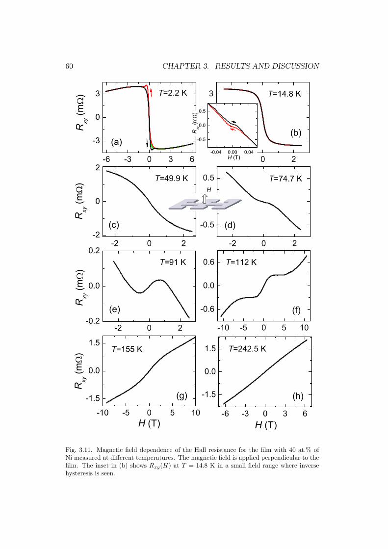
60 CHAPTER 3. RESULTS AND DISCUSSION
-6 -3 0 3 6
-3
0
3
T=2.2 K
(a)
-2 0 2
-3
0
3
T=14.8 K
(b)
-2 0 2-2
0
2
Rxy
(m)
Rxy
(m)
Rxy
(m)
Rxy
(m) T=49.9 K
(c)
-10 -5 0 5 10
-0.6
0.0
0.6
T=112 K
H
(f)
-2 0 2
-0.5
0.0
0.5
T=74.7 K
(d)
Rxy
(m)
-0.04 0.00 0.04
-0.5
0.0
0.5
H (T)
-2 0 2-0.2
0.0
0.2
T=91 K
(e)
-10 -5 0 5 10
-1.5
0.0
1.5
H (T)
H (T)
T=155 K
(g)
-6 -3 0 3 6
-1.5
0.0
1.5
T=242.5 K
(h)
Fig. 3.11. Magnetic field dependence of the Hall resistance for the film with 40 at.% ofNi measured at different temperatures. The magnetic field is applied perpendicular to thefilm. The inset in (b) shows Rxy(H) at T = 14.8 K in a small field range where inversehysteresis is seen.

3.2. MAGNETIC PROPERTIES OF PtNi THIN FILMS 61
-1 0 1
-20
-10
0
10
20
T =280 K
T =240 KT =180 K
T =120 K
Rxy
(m)
H (T)
T =1.8 K
H
filled symbol: H from + to -open symbol: H from - to +
67 at.% of Ni
Fig. 3.12. Magnetic field dependence of the Hall resistance for the film with 67 at.% of Ni,measured at different temperatures. The magnetic field is applied perpendicular to thefilm. The film shows high saturation Rxy with strong T dependence.
The peaks are smeared out already at T = 3.8 K, and the hysteresis van-ishes at T = 10.8 K. The hysteresis free shape of the Hall loop indicates anin-plane magnetization at this temperature. After that, another small “flat”hysteresis in the reverse, clockwise direction, appears at T = 14.8 K in thelow field region [see inset of Fig. 3.11(b)]. Such behavior is similar to thatobserved in Ref. [64], and is associated with restoring of the canted magneti-zation, with the easy axis flipping to the opposite side of the film, comparedto the low-T case. The competition between anisotropies of different do-mains results in an inverted hysteresis loop [64]. This hysteresis disappears atT ≃ 25 K. Upon further increase of temperature, the Rxy(H) curve becomesunsaturated [see Fig. 3.11(c)]. At T ≃ 75 K, a large plateau develops aroundzero field [see Fig. 3.11(d)]. At higher temperatures, the extraordinary Hallcoefficient changes the sign to negative, and the film becomes paramagneticat T ≃ 240 K. A behavior similar to that shown in Figs. 3.11(d) and 3.11(e),where Rxy displays the zero field slope and changes the sign of the slope atlow fields, was also reported in Refs. [91] and [92].
Figure 3.12 shows Rxy(H) at different temperatures for the film with thehighest studied Ni concentration of 67 at.%. The magnetic field is appliedperpendicular to the film. The measured curves show almost no hysteresisand a clear saturation. In contrast to the film with 40 at.% of Ni, the filmwith 67 at.% of Ni has a negative (electron-type) contribution from the EHEat all measured temperatures. The saturation value of Rxy at the lowest Tis seven times larger than for the film with 40 at.% of Ni, shown in Fig. 3.11.The film becomes paramagnetic at T ≃ 280 K.

62 CHAPTER 3. RESULTS AND DISCUSSION
-4 0 4
-2
0
2
-4 0 4
-2
0
2
-4 0 4
-2
0
2
-4 0 4
-2
0
2
-4 0 4
-2
0
2
-4 0 4
-2
0
2
90o
H
H
13 at.% of NiT=1.8 K
60o
Rxy
(m)
Rxy
(m)
Rxy
(m)
30o
(f)(e)
(d)(c)
(b)(a)
10o
H (T)
H (T)
5o
0o
Fig. 3.13. Magnetic field dependence of the Hall resistance for the film with 13 at.% of Nimeasured at T = 1.8 K for different angles between applied magnetic field and the samplesurface.
From Figs. 3.11 and 3.12 it is seen that although films with high Niconcentrations are clearly ferromagnetic in a wide temperature range andRxy(H) is dominated by the extraordinary contribution R1M , the observedcoercivity remains very small. As mentioned in subsection 1.4.3, such abehavior is expected for ferromagnetic films with in-plane orientation of theeasy axis of magnetization.
3.2.3 Angular dependence of the anomalous Hall effect
To study the orientation of the magnetic anisotropy the Hall effect was stud-ied at different angles between the field and the film surface.
Figures 3.13-3.16 show Rxy(H) curves at T ≃ 2 K for angles of (a) 90

3.2. MAGNETIC PROPERTIES OF PtNi THIN FILMS 63
-4 0 4
-1
0
1
-4 0 4
-1
0
1
-4 0 4
-1
0
1
-4 0 4
-1
0
1
-4 0 4
-1
0
1
-4 0 4
-1
0
1
90o
H
H
27 at.% of NiT=2.1 K
60o
Rxy
(m)
Rxy
(m)
Rxy
(m)
30o
(f)(e)
(d)(c)
(b)(a)
10o
H (T)
H (T)
5o
0o
Fig. 3.14. Magnetic field dependence of the Hall resistance for the film with 27 at.% of Nimeasured at T = 2.1 K for different angles between applied magnetic field and the samplesurface.
(field perpendicular to the film), (b) 60, (c) 30, (d) 10, (e) 5 and (f) 0
(field parallel to the film) between the magnetic field and the film surface forall studied Ni concentrations. The saturation Hall resistance decreases withdecreasing angle in all cases, since it is proportional to the magnetic momentperpendicular to the film. For the parallel field orientation the saturationRxy becomes almost zero.
Films with low Ni concentrations possessing out-of-plane magnetization(13 at.% and 27 at.% of Ni) show an increase of coercivity as the angle ofapplied field approaches the hard axis, which is in agrement with calculatedhysteresis loops reported in Ref. [93]. Near the hard axis, the coercivityis so large that the film is hardly saturated, and the hysteresis becomes

64 CHAPTER 3. RESULTS AND DISCUSSION
-4 0 4
-4
-2
0
2
4
-4 0 4
-4
-2
0
2
4
-4 0 4
-4
-2
0
2
4
-4 0 4
-4
-2
0
2
4
-4 0 4
-4
-2
0
2
4
-4 0 4
-4
-2
0
2
4
90o
H
H
40 at.% of NiT=2.1 K
60o
Rxy
(m)
Rxy
(m)
Rxy
(m)
30o
(f)(e)
(d)(c)
(b)(a)
10o
H (T)
H (T)
5o
0o
Fig. 3.15. Magnetic field dependence of the Hall resistance for the film with 40 at.% of Nimeasured at T = 2.1 K for different angles between applied magnetic field and the samplesurface.
invisible [see Fig. 3.13(f)]. As it is mentioned in Ref. [65], the hysteresis isvery sensitive to the angle between the film surface and the magnetic field,and the disappearance of the hysteresis can be seen for the angles less than1. This explains the hysteresis shown in Fig. 3.14(f) where the field is notperfectly parallel to the film surface.
The film with 40 at.% of Ni (Fig. 3.15) shows somewhat similar behavioras the films with 13 at.% and 27 at.% of Ni, except for the presence ofthe PHE. The contribution from the PHE slightly increases at intermediateangles followed by decreasing at 0.
The film with 67 at.% of Ni shows an abrupt switching of the Hall re-sistance in the low field region at the angle of 10 [see Fig. 3.16(d)]. As theangle decreases further towards the film surface, the value of Rxy between the
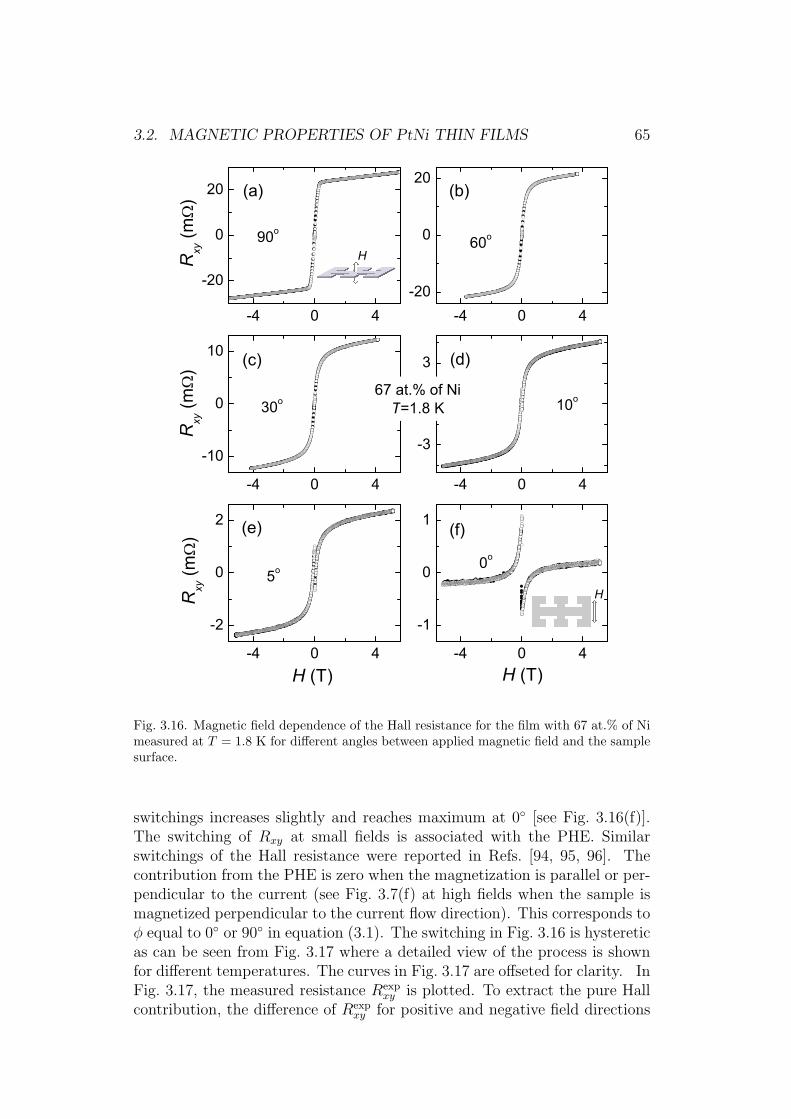
3.2. MAGNETIC PROPERTIES OF PtNi THIN FILMS 65
-4 0 4
-20
0
20
-4 0 4-20
0
20
-4 0 4
-10
0
10
-4 0 4
-3
0
3
-4 0 4
-2
0
2
-4 0 4
-1
0
1
90o
H
H
67 at.% of NiT=1.8 K
60o
Rxy
(m)
Rxy
(m)
Rxy
(m)
30o
(f)(e)
(d)(c)
(b)(a)
10o
H (T)
H (T)
5o
0o
Fig. 3.16. Magnetic field dependence of the Hall resistance for the film with 67 at.% of Nimeasured at T = 1.8 K for different angles between applied magnetic field and the samplesurface.
switchings increases slightly and reaches maximum at 0 [see Fig. 3.16(f)].The switching of Rxy at small fields is associated with the PHE. Similarswitchings of the Hall resistance were reported in Refs. [94, 95, 96]. Thecontribution from the PHE is zero when the magnetization is parallel or per-pendicular to the current (see Fig. 3.7(f) at high fields when the sample ismagnetized perpendicular to the current flow direction). This corresponds toϕ equal to 0 or 90 in equation (3.1). The switching in Fig. 3.16 is hystereticas can be seen from Fig. 3.17 where a detailed view of the process is shownfor different temperatures. The curves in Fig. 3.17 are offseted for clarity. InFig. 3.17, the measured resistance Rexp
xy is plotted. To extract the pure Hallcontribution, the difference of Rexp
xy for positive and negative field directions

66 CHAPTER 3. RESULTS AND DISCUSSION
-0.04 -0.02 0.00 0.02 0.04
0
2
4
6
8
67 at.% of Ni
Rexp
xy(m
)
H (T)
T =270 K
T =200 K
T =130 K
T =90 K
T =1.8 K
H
Fig. 3.17. Measured resistance in transverse direction at different temperatures as a func-tion of magnetic field for the film with 67 at.% of Ni. The magnetic field is applied parallelto the film surface and swept in a small range around zero. The curves are offseted forclarity.
0 5 10 15 20-0.8
-0.4
0.0
0.4
0.8
R* xy
(m)
H (mT)
T =1.8 K T =90 K T =130 K T =200 K T =270 K
Fig. 3.18. Hall resistance, subtracted from the measured resistance Rexpxy using equa-
tion (3.2), as a function of magnetic field for the same temperatures as in Fig. 3.17. Thecoercivity vanishes at T = 270 K.

3.3. MESOSCOPIC JOSEPHSON JUNCTIONS 67
2 4 6 8 10 12 140.0
0.2
0.4
0.6
0 50 100 150 200 2500.000
0.003
0.006
0.009
13 at.%
27 at.%C
oerc
ivity
(T)
T (K)
67 at.% @ 90o
T (K)C
oerc
ivity
(T)
Fig. 3.19. Coercivity estimated from RH vs H curves at different temperatures for thefilms with 13 (solid squares) and 27 (solid circles) at.% of Ni, with magnetic field appliedperpendicular to the film surface. The inset shows coercivity vs T for the film with 67at.% of Ni, with magnetic field applied parallel to the film surface.
is taken:
R∗xy =
[Rexpxy (+H)−Rexp
xy (−H)]
2. (3.2)
In this way the contribution from the longitudinal resistance, even with re-spect to the field direction, is canceled out. Figure 3.18 shows the pure Hallresistance R∗
xy as a function of magnetic field for the same temperatures asin Fig. 3.17. The hysteresis is observed up to T = 270 K, indicating thein-plane magnetization in this film.
Figure 3.19 summarizes the T -dependence of coercivity for the films withlow (main panel) and high (inset) Ni concentrations. It allows most accurateestimation of the blocking temperature Tb ≃ 7 and 13 K for the films with13 and 27 at.% of Ni, respectively, and Curie temperature TC ≃ 270 K forthe film with 67 at.% of Ni. Despite a dramatic increase of the transitiontemperature, the coercivity of the film with 67 at.% of Ni is much smallerthan that for films with low Ni concentrations. This is caused by reorientationof the magnetic anisotropy from out-of-plane to in-plane with increasing Niconcentration.
3.3 Mesoscopic Josephson junctions
In this section the results which are partially included in the papers I-V willbe presented. However, significant parts of the data from this section did notappear in any of the appended publications.

68 CHAPTER 3. RESULTS AND DISCUSSION
4 5 6 7 8 9 100
1
2
3
4
5
6
7
Nb-Pt0.40
Ni0.60
-Nb
Tc of upper andlower Nb layers
R
()
T (K)
2 4 60
50
100 Nb-Pt0.40
Ni0.60
-Nb
I c ( A
)
T (K)
0
3
6
9
12
Nb-Cu-Nb
Fig. 3.20. T -dependence of the normal state resistance for the Nb-Pt0.40Ni0.60-Nb and Nb-Cu-Nb Josephson junctions. The resistance above Tc is the resistance of the Nb electrode.The two transition temperatures of the Nb-Pt0.40Ni0.60-Nb junction at ∼ 8.8 and ∼ 8.6K correspond to Tc of the upper and lower Nb layers, respectively. The inset showsT -dependence of the critical current density for the Nb-Pt0.40Ni0.60-Nb junction.
3.3.1 Basic characteristics
The main panel of Fig. 3.20 shows a resistive transition of the 3D FIB sculp-tured Nb-Pt0.40Ni0.60 (20 nm)-Nb and planar Nb-Cu-Nb junctions. Abovethe superconducting critical temperature Tc, the resistance is predominantlythe resistance of the Nb bridge (see schematic pictures of the junctions inFig. 2.9). The Nb-Pt0.40Ni0.60-Nb junction has Tc ≃ 9 K which is higher thanTc ≃ 7 K of the Nb-Cu-Nb. The difference in Tc and also different normalstate resistances of the leads, 6 Ω for Nb-Pt0.40Ni0.60-Nb junction and 11.3 Ωfor Nb-Cu-Nb junction, are due to the different thicknesses of the Nb layersin those two types of junctions. From Fig. 3.20 one can see that the resis-tance of the bridge of the Nb-Pt0.40Ni0.60-Nb junction first drops abruptly at∼ 8.8 K and then at ∼ 8.6 K. These temperatures represent Tc of the upperand lower Nb layers, respectively. The difference between Tc is because ofthe different structure of the two Nb layers due to the substrate effect onthe lower Nb layer and, to some extent, due to different thicknesses of Nblayers and correspondingly the different influence of the proximity effect inthe Pt0.40Ni0.60 interlayer. The resistive transition of the junction itself isimpossible to see on the main panel of Fig. 3.20. The critical temperatureof the junction with 60 % of Ni (the temperature at which critical currentbecame measurable) is defined from the dependence of the junction criticalcurrent on the temperature (inset of Fig. 3.20) to ∼ 5 K. The Tc of the Nb-Pt1−xNix-Nb junction depends on the Ni concentration and becomes almost

3.3. MESOSCOPIC JOSEPHSON JUNCTIONS 69
-0.2 0.0 0.2
-0.4
0.0
0.4
H=0 TT~3 K
I (m
A)
V (mV)
Nb-Pt1.00Ni0.00-Nb (170 88 nm2)
Nb-Pt0.60Ni0.40-Nb (225 640 nm2)
-0.05 0.00 0.05
planar Nb-Cu-Nb
Fig. 3.21. I−V characteristics of the Nb-Pt1−xNix-Nb junctions with x = 0 (full squares),x = 40 (open circles), and the Nb-Cu-Nb planar junction (open squares) in the absence ofexternal magnetic field and at T ≃ 3 K. The voltage for the Nb-Cu-Nb junction is plottedit the top axis. The values of Rn are 0.6 Ω and 0.4 Ω for the junctions with 0 at.% and40 at.% of Ni, respectively. The planar Nb-Cu-Nb junction has Rn ≃ 0.1 Ω.
8 K for the junctions with zero Ni concentration.
The most basic measurement one can perform on a Josephson junction isa current-voltage characterization. Figure 3.21 shows I−V curves of the Nb-Pt1−xNix-Nb junctions with x = 0 (full squares) and x = 40 (open circles),and a Nb-Cu-Nb planar junction (open squares, top axis) in the absence ofexternal magnetic field and at a temperature of about 3 K. The thickness ofthe PtNi interlayer in the Nb-Pt1−xNix-Nb junctions is 30 nm. The I − Vcharacteristics of measured junctions are well described by the resistivelyand capacitively shunted junction (RCSJ) model (see subsection 1.2.3). Thenormal state resistances Rn are 0.6 Ω and 0.4 Ω for the junctions with 0at.% and 40 at.% of Ni, respectively. The value of Rn provides the value ofresistivity for PtNi alloys which is ranging from ∼ 25 µΩcm for pure Pt toseveral hundreds µΩcm for the junctions with a high Ni concentration. TheRn of the Nb-Cu-Nb junction is much smaller (∼ 0.1 Ω) due to a relativelylarge junction length (see subsection 2.1.3). In the appendix A, the resistivityand some other characteristics of all measured Nb-Pt1−xNix-Nb junctions arepresented.
Figure 3.22 shows the critical current density Jc of the Nb-Pt1−xNix-Nb overlap type junctions plotted in semi-logarithmic scale as a function ofT (left panel) and
√T (right panel) for different Ni concentrations. From
Fig. 3.22 it is seen that the critical current density has a strong temperature

70 CHAPTER 3. RESULTS AND DISCUSSION
1 2 3 4 5 6 7 8101
102
103
104
105
106
107
J c (A
)
T (K)
0 at.% of Ni 20 at.% of Ni 54 at.% of Ni (low IC) 54 at.% of Ni (high IC) 60 at.% of Ni (low IC) 60 at.% of Ni (high IC)
1.5 2.0 2.5101
102
103
104
105
106
107
J c (A
)
sqrt(T) (K)1/2
0 at.% of Ni 20 at.% of Ni 54 at.% of Ni (low IC) 54 at.% of Ni (high IC) 60 at.% of Ni (low IC) 60 at.% of Ni (high IC)
Fig. 3.22. Dependence of the critical current densities on the temperature (left) and thesquare root of temperature (right) in semi-logarithmic scale for junctions with 0, 20, 54and 60 at.% of Ni. Jc has a strong dependence on T and
√T . Jc(T ) becomes exponential
for 54 and 60 at.% of Ni.
dependence. Jc(T ) becomes exponential for high Ni concentrations. Sucha temperature dependence is typical for S-N-S proximity coupled junctions,in which the thickness of the normal metal exceeds the coherence lengthξN [98]. In this case, the temperature dependence of Jc is determined bythe temperature dependence of the coherence length in the barrier. If so, ξFfor the junctions with strong ferromagnetic barrier should also have a strongtemperature dependence. Figure 3.23 shows ξF as a function of 1/T (leftpanel) and 1/
√T (right panel) calculated from Jc(T ) using the expression
for temperature dependence of Jc in S-N-S junctions:
Jc(T ) ∝ Jc(0) exp
(− t/2
ξF (T )
). (3.3)
0.1 0.2 0.3 0.4 0.5 0.6
1
2
3
4
5
6 54 at.% of Ni (low Ic) 54 at.% of Ni (high Ic) 60 at.% of Ni (low Ic) 60 at.% of Ni (high Ic)
cohe
rent
leng
th (n
m)
1/T (1/K)0.3 0.4 0.5 0.6 0.7 0.8
1
2
3
4
5
6
cohe
rent
leng
th (n
m)
1/sqrt(T) (1/K)1/2
54 at.% of Ni (low Ic) 54 at.% of Ni (high Ic) 60 at.% of Ni (low Ic) 60 at.% of Ni (high Ic)
Fig. 3.23. 1/T (left) and 1/√T (right) dependence of the coherence lengths in the fer-
romagnetic barrier layer of the Nb-PtNi-Nb junctions with 54 and 60 at.% of Ni. Thecoherent length is calculated from expression (3.3).
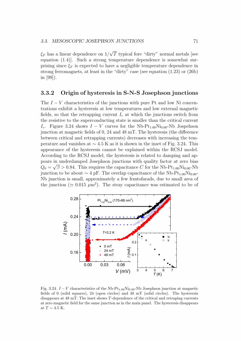
3.3. MESOSCOPIC JOSEPHSON JUNCTIONS 71
ξF has a linear dependence on 1/√T typical fore “dirty” normal metals [see
equation (1.4)]. Such a strong temperature dependence is somewhat sur-prising since ξF is expected to have a negligible temperature dependence instrong ferromagnets, at least in the “dirty” case (see equation (1.23) or (26b)in [99]).
3.3.2 Origin of hysteresis in S-N-S Josephson junctions
The I − V characteristics of the junctions with pure Pt and low Ni concen-trations exhibit a hysteresis at low temperatures and low external magneticfields, so that the retrapping current Ir at which the junctions switch fromthe resistive to the superconducting state is smaller than the critical currentIc. Figure 3.24 shows I − V curves for the Nb-Pt1.00Ni0.00-Nb Jospehsonjunction at magnetic fields of 0, 24 and 48 mT. The hysteresis (the differencebetween critical and retrapping currents) decreases with increasing the tem-perature and vanishes at ∼ 4.5 K as it is shown in the inset of Fig. 3.24. Thisappearance of the hysteresis cannot be explained within the RCSJ model.According to the RCSJ model, the hysteresis is related to damping and ap-pears in underdamped Josephson junctions with quality factor at zero biasQ0 =
√β > 0.84. This requires the capacitance C for the Nb-Pt1.00Ni0.00-Nb
junction to be about ∼ 4 pF. The overlap capacitance of the Nb-Pt1.00Ni0.00-Nb junction is small, approximately a few femtofarads, due to small area ofthe junction (≃ 0.015 µm2). The stray capacitance was estimated to be of
0.00 0.03 0.06 0.09 0.12 0.15
0.16
0.20
0.24
0.28
3 4 5 6 7
0.1
0.2
T=3.2 K
Pt1.00
Ni0.00
(170 88 nm2)
V (mV)
I (m
A)
0 mT24 mT48 mT
Ic Ir
T (K)
I (m
A)
Fig. 3.24. I −V characteristics of the Nb-Pt1.00Ni0.00-Nb Josephson junction at magneticfields of 0 (solid squares), 24 (open circles) and 48 mT (solid circles). The hysteresisdisappears at 48 mT. The inset shows T -dependence of the critical and retraping currentsat zero magnetic field for the same junction as in the main panel. The hysteresis disappearsat T ∼ 4.5 K.
72 CHAPTER 3. RESULTS AND DISCUSSION
the same order of magnitude. Therefore, the total C of this junction is insuf-ficient for observing a hysteresis within the RCSJ model. Another origin forthe hysteresis can be a self-heating phenomenon [97]. Within the self-heatingscenario, the retrapping current simply represents Ic at the elevated temper-ature due to power dissipation at the resistive branch of the I−V curve. Oneway to check the origin of the hysteresis is to study the power dissipation de-pendence of Ir. It turns out that the self-heating scenario as well cannot fullyexplain the presence of the hysteresis in this junction. In general, a hysteresisin I − V curves is quite common phenomenon in S-N-S type of Josephsonjunctions and can be attributed to non-equilibrium phenomena or frequencydependent damping. More details about the origin of the hysteresis in theNb-Pt1.00Ni0.00-Nb junction can be found in the appended paper I.
3.3.3 Magnetic characterization of S-F-S and planarS-N-S Josephson junctions
The right panel of Fig. 3.25 shows the dependence of Ic on the in-plane mag-netic field H|| (Fraunofer pattern) for the junction with a size of 1140×230nm2, a Ni concentration of 54 at.% and a barrier layer thickness of 20 nm.The field was applied across the longer (1140 nm) side. In general, the fieldcan be applied in either x-direction or y-direction, as it is shown in the leftpanel of Fig. 3.25, depending on the chip orientation on the plug-in. Themeasured Ic(H||) curve is in very good agreement with a calculated field de-pendence of Ic (solid line in the right panel of Fig. 3.25). From the Fraunoferpattern in Fig. 3.25 the magnetic thickness of the Nb-Pt0.46Ni0.54-Nb junctioncan be estimated dmagn ≃ 214 nm, where ∆H ≃ 8.5 mT is the periodicityof the Fraunhofer pattern. Using equations (1.8) and (1.16) one can findλJ ≃ 392 nm and λ ≃ 118 nm. λ has the same order of magnitude for dif-ferent junctions while λJ is different for different junctions depending on theNi concentration and thickness of the junction barrier layer. This is becauseλJ is inversely proportional to the square root of critical current density [seeequation (1.8)]. The values of λJ ranging between hundreds of nm to severalµm for the studied overlap type junctions.
Figure 3.26 shows the Fraunhofer patterns for the Nb-Pt1−xNix-Nb junc-tions with 13, 20, 27 and 40 at.% of Ni. In order to compare the differentjunctions with different properties and geometries, the critical current den-sity is plotted as a function of the total magnetic flux through the junctionplane normalized to magnetic flux quanta. The critical current density van-ishes when the total magnetic flux is equal to an integer number of Φ0 (seesubsection 1.2.4).
Figure 3.27 shows the field dependence of Ic for the Nb-Cu-Nb planarjunction. The typical length of the fabricated planar junctions is ∼ 6µm.Since the total magnetic flux through the junction is proportional to thejunction length (see subsection 1.2.4), the field needed to get one flux quanta

3.3. MESOSCOPIC JOSEPHSON JUNCTIONS 73
-0.06 -0.03 0.00 0.03 0.06
-2
-1
0
1
2 Pt0.46
Ni0.54
(1140 230 nm2)T=1.8 K
I C (m
A)
H (T)
Fig. 3.25. Left: Scheme of the magnetic field experiment. Right: Ic(H||) modulation ofthe Nb-Pt0.46Ni0.54-Nb Josephson junction. The field is applied across the side of thelength of 1140 nm. The solid line represents calculated Ic(H||) using equation (1.17) andan experimental value of dmagn.
-3 -2 -1 0 1 2 30.00
0.02
0.04
0.06
0.08
J C (1
05 A/c
m2 )
/ 0
x=13 % x=20 % x=27 % x=40 %
T~3 K
Nb-Pt1-xNix-Nb
Fig. 3.26. Jc as a function of Φ/Φ0 for the junctions with 13, 20, 27 and 40 at.% of Ni.Jc vanishes when the total magnetic flux is equal to an integer number of Φ0. The goodquality of the Fraunhofer patterns can serve as an evidence for uniformity of the propertiesof the junctions and monodomain structure of the ferromagnetic layer.

74 CHAPTER 3. RESULTS AND DISCUSSION
-0.2 0.0 0.2-0.4
-0.2
0.0
0.2
0.4
I c (m
A)
H (mT)
T~3.5 K
planar Nb-Cu-Nb
Fig. 3.27. Ic as a function of in-plane magnetic field for the Nb-Cu-Nb planar junction.The large (∼ 6 µm) junction length results in a high sensitivity to the applied magneticfield.
through the junction is much smaller for planar junctions. This results in ahigh sensitivity of the junction critical current to the applied field in com-parison with overlap type Nb-Pt1−xNix-Nb junctions (see the right panel inFig. 3.25).
Figure 3.28 characterizes another Nb-Pt1−xNix-Nb junction with the high-est measured Ni concentration of 67 at.%. The size of the junction is 120×350 nm2 which is too small to detect any Ic. Instead, the resistance ofthe junction Rn was measured with the software-based lock-in amplifier (seesubsection 2.2.2). The applied bias current was 2.26 · 10−5 A, and Rn wasmeasured at the maximum bias current. The Rn modulation shows the samebehavior as the Ic(H||) modulation. The maximum Rn, when there is no con-tribution to the resistance from the supercurrent, corresponds to an integernumber of Φ0 through the junction plane.
There are no visible distortions or asymmetries in the Fraunhofer patternsand the Rn(H||) modulation. This can serve as an evidence for uniformity ofthe properties of the junctions and monodomain structure of the ferromag-netic layer.
As it was mentioned in subsection 2.1.3, one should overmill in to theupper Nb layer for some depth in order to avoid the undercut of the bottomNb layer. Such an undercut will lead to the appearance of excess currentwhich is flowing not through the junction barrier as schematically shown inthe left inset of Fig. 3.29. Sometimes it was still difficult to determine thedepth of overmilling with a good accuracy due to the several reasons:
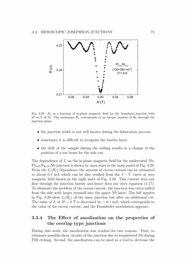
3.3. MESOSCOPIC JOSEPHSON JUNCTIONS 75
-0.08 -0.04 0.00 0.04 0.080.21
0.24
0.27
Pt0.33Ni0.67
(120 350 nm2)T=1.8 KR
(
H (T)
Fig. 3.28. Rn as a function of in-plane magnetic field for the Josephson junction with67 at.% of Ni. The maximum Rn corresponds to an integer number of Φ0 through thejunction plane.
• the junction width is not well known during the fabrication process;
• sometimes it is difficult to recognize the barrier layer;
• the drift of the sample during the milling results in a change of theposition of a ion beam for the side cut.
The dependence of Ic on the in-plane magnetic field for the undercuted Nb-Pt0.87Ni0.13-Nb junction is shown by open stars in the main panel of Fig. 3.29.From the Ic(H||) dependence the amount of excess current can be estimatedto about 0.1 mA which can be also verified from the I − V curve at zeromagnetic field shown in the right inset of Fig. 3.29. This current does notflow through the junction barrier and hence does not obey equation (1.17).To eliminate the problem of the excess current, the junction was extra milledfrom the side with larger overmill into the upper Nb layer. The full squaresin Fig. 3.29 show Ic(H||) of the same junction but after an additional cut.The value of Ic at H = 0 T is decreased by ∼ 0.1 mA, which corresponds tothe value of the excess current, and the Fraunhofer modulation appears.
3.3.4 The Effect of anodization on the properties ofthe overlap type junctions
During this work, the anodization was studied for two reasons. First, toeliminate possible short circuits of the junction due to resputtered Nb duringFIB etching. Second, the anodization can be used as a tool to decrease the

76 CHAPTER 3. RESULTS AND DISCUSSION
-0.2 0.0 0.20.0
0.1
0.2
0.3
0.4
Pt0.87Ni0.13
(180 218 nm2)T~3 K
I C (m
A)
H (T)
before additional cut after additional cut after additional cut
and anodization
-0.1 0.0 0.1
-0.5
0.0
0.5
Nb
Nb
PtNi Josephson current
excess current I C (m
A)
V (mV)
Fig. 3.29. Ic(H||) modulation of the Nb-Pt0.87Ni0.13-Nb Josephson junction. The curve,shown by open stars, indicates that there is an excess current of ∼ 0.1 mA which flow notthrough the junction barrier. The additional cut removes the remaining Nb material in thelower Nb electrode resulting in the improvement of Ic(H||) modulation (full squares). Theanodization further improves the Ic(H||) (open circles). The left inset shows the schematicpicture of the junction side view where the arrows indicate the Josephson supercurrentand excess current through the remaining Nb material in the lower electrode. The rightinset shows I−V curve for the same junction before and after additional cut at H|| = 0 T.
-0.08 -0.04 0.00 0.04 0.08
0.00
0.06
0.12
0.18
I C (m
A)
H (T)
Pt0.80Ni0.20
(319 117 nm2)across long side
T~3.2 K
before anodizationafter anodization
Fig. 3.30. Ic(H||) modulations of the junction with 20 at.% of Ni before (full squares)and after (open circles) anodization. The field was applied across the long (319 nm) side.From the difference in the periodicity of Ic(H||) before and after anodization, the depthof anodization was estimated to ∼ 30 nm.

3.3. MESOSCOPIC JOSEPHSON JUNCTIONS 77
effective size of the junction. As it can be seen from the main panel ofFig. 3.29, the anodization further improves the Fraunhofer pattern after anadditional cut, indicating that there were some remaining short circuits. TheIc(H||) after anodization is shown in Fig. 3.29 by open circles. The increaseof ∆H after anodization from ∼ 81 to ∼ 85 mT corresponds to change inthe size of the junction side, from 180 to 172 nm, across which the field wasapplied. This effective size corresponds to the total size minus the depth ofthe anodized layer.
Figure 3.30 shows Ic(H||) at T ∼ 3.2 K for another junction with 20 at.%of Ni before and after anodization. The initial size of the junction was319×117 nm. From the change in periodicity of the Fraunhofer pattern thedepth of anodization can be estimated to ∼ 30 nm.
3.3.5 0 – π transition in S-F-S overlap type junctions
Figure 3.31 summarizes the study of various Nb-Pt1−xNix-Nb Josephson junc-tions. It shows the critical current density at T = 3.1−3.2 K as a function ofNi concentration. Jc decreases with increasing the Ni concentration from 0to 40 at.%. For larger Ni content (54 and 60 at.%) the maximum Jc becomeslarger, before it becomes unmeasurably small in the case of 67 at.% of Ni.Such a non-monotonic behavior can be due to switching into the π state [11]as a function of Ni concentration. At the same time, S-F-S junctions withsimilar geometry on the same chip with 54 and 60 at.% of Ni could exhibita large spread in Jc as marked in Fig. 3.31, presumably due to considerable
10 20 30 40 50 60 700
4
8
12
16
32
36
T~3K
J c (1
05 A/c
m2 )
Ni concentration (at.%)
d=20 nmd=20 nmd=20 nmd=25 nmd=24 nmd=30 nm
0
Fig. 3.31. Critical current density of the Nb-Pt1−xNix-Nb Josephson junctions for allmeasured Ni concentrations. The non-monotonic behavior of Jc can be due to switchinginto the π state as a function of Ni concentration.

78 CHAPTER 3. RESULTS AND DISCUSSION
-0.2 0.0 0.20.0
0.2
0.4
0.6 Pt0.46Ni0.54
T=1.8 K
1140 230 nm2
I c (m
A)
H (T)
0.03
0.04
0.05
0.06
800 225 nm2
0.00 0.02 0.04
0.4
0.8
1.2
Pt0.40Ni0.60
T=1.8 K
1200 300 nm2
0.04
0.08
0.121050 420 nm2
H (T)
I c (m
A)
Fig. 3.32. Left: Ic(H||) modulations for the junctions with low (open symbols, rightaxis) and high (solid symbols, left axis) Jc and a Ni concentration of 54 at.%. Right:Ic(H||) modulations for the junctions with low (open symbols, right axis) and high (solidsymbols, left axis) Jc and a Ni concentration of 60 at.%. The modulation of Ic can beclearly distinguished in all cases and the periods of modulation are in agreement with thejunction cross sections. All this confirms the quality of the junctions. H|| was appliedacross the long side for all junctions.
stray fields from the ferromagnet layers in the electrodes.Each panel in Fig. 3.32 shows the Fraunhofer modulation for the junctions
with the same Ni concentration (left panel for 54 at.% and right panel for60 at.% of Ni) which show low (open symbols, right axis) and high (solidsymbols, left axis) Jc, as marked in Fig. 3.31. H|| is applied across the longside for all junctions. The modulation of Ic can be clearly distinguishedin all cases. The junctions with the same Ni concentrations have similar
20 25 30
4
8
12
27 at.% of Ni
20 at.% of Ni
13 at.% of Ni
J c (1
05 A/c
m2 )
thickness (nm)
Fig. 3.33. Critical current density as a function of the Pt1−xNix barrier thickness fordifferent Ni concentration in the barrier layer.

3.3. MESOSCOPIC JOSEPHSON JUNCTIONS 79
periods of modulation, which is in agrement with the junction cross sections,but very different Ic.
Interestingly, the junctions with high Jc (shown in Fig. 3.31 by opendiamonds) had a spontaneous jump from low to the present value of Jc. Jcbefore the jump had a value similar to Jc of the corresponding junction withthe same (54 or 60 at.%) Ni concentrations but low Jc shown by open trianglesin Fig. 3.31. The jump in Jc was accompanied by a jump in resistivity. Theresistivity increased about tree times to 262 and 342 µΩcm for the junctionswith 54 and 60 at.% of Ni, respectively.
Figure 3.33 shows Jc as a function of the barrier layer thickness for thejunction with 13, 20 and 27 at.% of Ni. Jc monotonically decreases withincreasing of thickness in all cases.
3.3.6 Application of mesoscopic Josephson junction asphase sensitive detectors
The vortex state in mesoscopic systems can be probed, e.g., by Hall-probemeasurements [100], point-contact techniques [101], scanning tunnel micro-scopy [102], scanning superconducting quantum interference device micro-scopy [103], magnetic force microscopy [104], or Bitter decoration [105]. Here,the fabricated Josephson junctions are used as phase sensitive detectors foranalysis of vortex states.
Figure 3.34 shows the Fraunhofer modulation of an overlap type junctionof size 207×104 nm2 with a pure Pt barrier for different sweeping directionsof the magnetic field. The magnetic field was applied across the junction sideof 207 nm. At certain fields, the smooth Fraunhofer pattern is interruptedby jumps in Ic. Each jump in the Fraunhofer pattern corresponds to theentrance or exit of a vortex into the upper or lower superconducting electrode(see Fig. 2.13). The vortex induces a flux shift ∆Φ in the Ic(H||) modulation.In mesoscopic junctions, the vortex enters at a higher field than it exits. Thiscauses metastability upon changing the field sweeping direction which leadsto the hysteresis of the Ic(H||) modulations as seen in Fig. 3.34. The vorticesstart to enter at a field ∼ 0.25 T while upon sweeping back they start to exitat a field ∼ 0.15 T.
As it was mentioned in section 1.3, the vortex is a source of a vectorpotential A which, in turn, induces a global 2π phase rotation in the su-perconducting condensate. This is a consequence of the Aharonov-Bohmeffect [36]. Now, if a junction is introduced as it is shown schematically inFig. 1.4, the change of the phase within the junction length can be writtenas (see section 1.3)
Θv(x) = arctan
(x− xv
zv
)+ const., (3.4)
where xv and zv are the vortex coordinates and x is the position along the
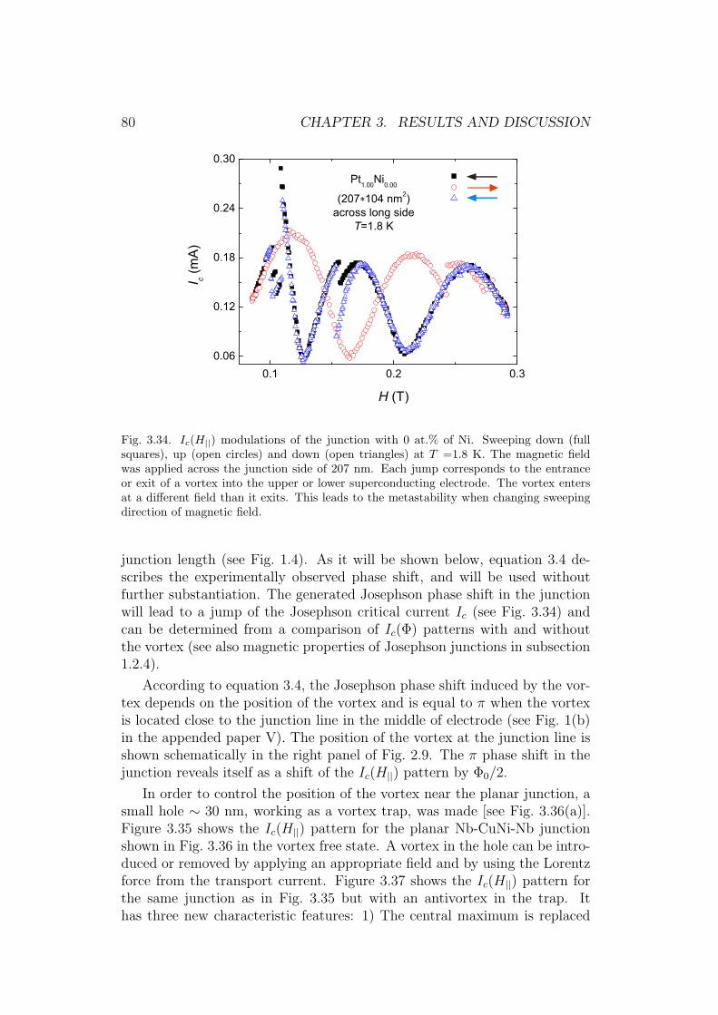
80 CHAPTER 3. RESULTS AND DISCUSSION
0.1 0.2 0.30.06
0.12
0.18
0.24
0.30
I c (m
A)
H (T)
Pt1.00Ni0.00
(207 104 nm2)across long side
T=1.8 K
Fig. 3.34. Ic(H||) modulations of the junction with 0 at.% of Ni. Sweeping down (fullsquares), up (open circles) and down (open triangles) at T =1.8 K. The magnetic fieldwas applied across the junction side of 207 nm. Each jump corresponds to the entranceor exit of a vortex into the upper or lower superconducting electrode. The vortex entersat a different field than it exits. This leads to the metastability when changing sweepingdirection of magnetic field.
junction length (see Fig. 1.4). As it will be shown below, equation 3.4 de-scribes the experimentally observed phase shift, and will be used withoutfurther substantiation. The generated Josephson phase shift in the junctionwill lead to a jump of the Josephson critical current Ic (see Fig. 3.34) andcan be determined from a comparison of Ic(Φ) patterns with and withoutthe vortex (see also magnetic properties of Josephson junctions in subsection1.2.4).
According to equation 3.4, the Josephson phase shift induced by the vor-tex depends on the position of the vortex and is equal to π when the vortexis located close to the junction line in the middle of electrode (see Fig. 1(b)in the appended paper V). The position of the vortex at the junction line isshown schematically in the right panel of Fig. 2.9. The π phase shift in thejunction reveals itself as a shift of the Ic(H||) pattern by Φ0/2.
In order to control the position of the vortex near the planar junction, asmall hole ∼ 30 nm, working as a vortex trap, was made [see Fig. 3.36(a)].Figure 3.35 shows the Ic(H||) pattern for the planar Nb-CuNi-Nb junctionshown in Fig. 3.36 in the vortex free state. A vortex in the hole can be intro-duced or removed by applying an appropriate field and by using the Lorentzforce from the transport current. Figure 3.37 shows the Ic(H||) pattern forthe same junction as in Fig. 3.35 but with an antivortex in the trap. Ithas three new characteristic features: 1) The central maximum is replaced

3.3. MESOSCOPIC JOSEPHSON JUNCTIONS 81
-1.4 -0.7 0.0 0.7 1.4-80
-40
0
40
80with trap and without drain
I c (A
)
H (mT)
No vortexNb-CuNi-NbT=1.6 K
-2 -1 0 1 2
25
50with trap and drainT=1.6 K
H (mT)
I c (A
)
-2 -1 0 1 2
30
60
without trap and drainT=1.9 K
I c (A
)
H (mT)
Fig. 3.35. Ic(H||) modulation for the planar Nb-CuNi-Nb junction shown in Fig. 3.36,after the vortex trap was drilled but before the stray field drain was made. The clearFraunhofer pattern indicates the vortex free state over the whole measured field range.Left inset: Ic(H||) modulation before the vortex trap and field drain were made. Rightinset: Ic(H||) modulation after the vortex trap and field drain were made. No differencebetween the patterns indicate that the modifications made to the junction do not effectthe junction properties.
1 m
vortex trap
~ 30 nm
stray field
drain
~ 20 nm
xy
z
1 m
Nb-CuNi-Nb
planar junction
(a)
(b)
Fig. 3.36. SEM images of the planar Nb-CuNi-Nb junction with the vortex trap only (a)and with the trap and the stray field drain (b). The diameter of the vortex trap is ∼30 nm.

82 CHAPTER 3. RESULTS AND DISCUSSION
-1.2 -0.6 0.0 0.6 1.2
-80
-40
0
40
80
With field drainWithout field drain
Nb-CuNi-Nb
T=1.6 K
Antivortex in the hole
I c (
µA)
H (mT)
-60
-30
0
30
60
Fig. 3.37. Ic(H||) modulation for the same junction as in Fig. 3.35 but with an antivortexin the trap before (left axis) and after (right axis) the stray field drain was made. Sketchesdemonstrate junction sample geometries: with the vortex hole only and with the hole andthe stray field drain.
by a minimum; 2) The Ic(H||) modulation is out-of-phase with that for thevortex-free pattern, i.e., ∆Φ ≃ Φ0/2; 3) The periodicity of Ic(H||) modu-lation doubles at the left side of the pattern, leading to a clear left-rightasymmetry. When a vortex is trapped in the hole, instead of an antivortex,the Ic(H||) pattern becomes mirror reflected with respect to the H|| = 0 axis(see Fig. 3.38). These are well known fingerprints of 0 – π junctions with astep-like π-shift in the Josephson phase difference within the junction.
To verify that the observed behavior is not related to a stray field fromthe vortex, a stray field drain was etched through the Nb-CuNi bilayer in thevicinity of the vortex hole [see Fig. 3.36(b)]. The drain should substantiallydecrease the magnetostatic stray fields from the vortex at the junction. Fig-ure 3.37 (right axis) shows the Ic(H||) modulation after such a modificationwas made to the junction. The stray field drain does not affect the Ic(H||)pattern and the offset ∆Φ. This clearly shows that the effective trapped fluxin the junction is not driven by the simple magnetostatic spreading of thevortex stray field. Both, drilling the vortex hole and making the stray fielddrain do not affect the junction properties. This can be verified from the leftand right insets in Fig. 3.35 where Ic(H||) patterns are plotted before andafter all modifications were made. Scanning with FIB during preparationto the modification resulted in uniform milling of the sample, which slightlyreduces the critical current.
The left panel of Fig. 3.39 shows Ic(H||) patterns for the planarNb-Cu-Nb junction with the vortex trap made at the distance ≃ 1 µm (see

3.3. MESOSCOPIC JOSEPHSON JUNCTIONS 83
-2 -1 0 1 2-60
-30
0
30
60
Nb-CuNi-NbT=1.6 K
Vortex in the holeI c (
A)
H (mT)
Fig. 3.38. Ic(H||) modulation for the same junction as in Fig. 3.35 but with a vortex inthe trap. The Ic(H||) pattern becomes mirror reflected with respect to the H|| = 0 axis incomparison with the case when an antivortex is trapped (see Fig. 3.37).
the right panel of Fig. 3.39) with and without a vortex in the trap. TheIc(H||) modulation with a vortex shows a similar left-right asymmetry as inFigs. 3.37 and 3.38. Using equation (3.4) one can calculate the junction phaseshift induced by the vortex. For the case shown in Fig. 3.39 ∆Θv ≃ 0.76π.The polar angle of the vortex Θv(x) along the junction length is plotted inthe inset of Fig. 3.40 (right). Figure 3.40 shows measured (left panel) andcalculated (right panel) Ic(H||) patterns with an antivortex in the trap. Clear
-3 -2 -1 0 1 2 3-1.0
-0.5
0.0
0.5
1.0
Vortexin the holeNo vortex
Nb-Cu-NbT =2.5 K
/ 0
I c / I c0
Nb-Cu-Nb
planar junction
1 m
vortex trap
Fig. 3.39. Left: Ic(H||) modulations for the Nb-Cu-Nb junction with the vortex trap madeat the distance ≃ 1 µm (see SEM image in the right panel) with and without a vortex inthe trap.

84 CHAPTER 3. RESULTS AND DISCUSSION
-3 -2 -1 0 1 2 3-1.0
-0.5
0.0
0.5
1.0
Nb-Cu-NbT =2.5 K
Antivortexin the hole
(experiment)
/ 0
I c / I c0
-3 -2 -1 0 1 2 3-1.0
-0.5
0.0
0.5
1.0Antivortexin the hole
(theory)
I c / I c0
/ 010 0
v (x)
x/L
zv/L=0.19
Fig. 3.40. Left: The same Nb-Cu-Nb junction as in Fig. 3.39 but with an antivortex inthe trap. Right: Calculated Ic(H||) pattern for the junction with an antivortex in theposition xv = L/2 and zv = 0.19L, where L is the junction length. The inset shows thecalculated polar angle, equation (3.4), of the vortex Θv(x) along the junction length. Theposition of the vortex in the calculations is the same as the position of the vortex trap inthe experiment.
agreement of the measured curve with the calculated one is seen.
Figure 3.41 (left panel) shows the Ic(H||) modulation for the Nb-Cu-Nbsquid without and with an antivortex in the trap. The close position of thevortex trap [see SEM image in Fig. 3.41 (right panel)] results in the Φ0/2shift of the Fraunhofer pattern when the (anti)vortex is trapped.
To get more insight into the influence of the junction geometry on ∆Φ,mesoscopic Nb-PtNi-Nb junctions were used, where the vortex is geomet-rically confined in the middle of the electrodes, (zv ≃ d/2, xv ≃ L/2).
-2 -1 0 1 2-90
-60
-30
30
60
90
/ 0
No vortex
Antivortexin the hole
Nb-Cu-Nb squid T =3.4 KI c (
A)
1 mNb-Cu-Nb
squid
SiO2
Nbvortex trap
Fig. 3.41. Left: Ic(H||) modulation for the Nb-Cu-Nb squid without and with an antivortexin the trap. Right: SEM image of the Nb-Cu-Nb squid with the vortex trap close to thejunction lines.
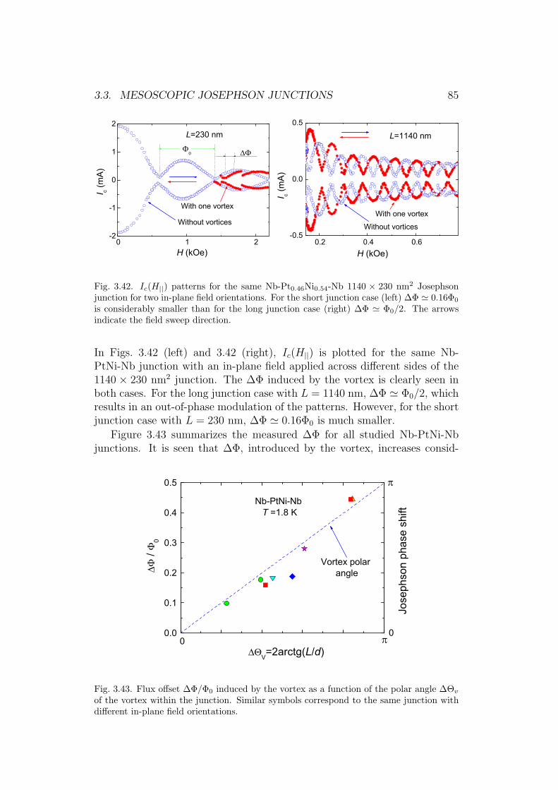
3.3. MESOSCOPIC JOSEPHSON JUNCTIONS 85
0 1 2-2
-1
0
1
2
I c (mA
)
With one vortex
Without vortices
L=230 nm
H (kOe)0.2 0.4 0.6
-0.5
0.0
0.5
I c (mA
)
L=1140 nm
H (kOe)
With one vortex
Without vortices
Fig. 3.42. Ic(H||) patterns for the same Nb-Pt0.46Ni0.54-Nb 1140 × 230 nm2 Josephsonjunction for two in-plane field orientations. For the short junction case (left) ∆Φ ≃ 0.16Φ0
is considerably smaller than for the long junction case (right) ∆Φ ≃ Φ0/2. The arrowsindicate the field sweep direction.
In Figs. 3.42 (left) and 3.42 (right), Ic(H||) is plotted for the same Nb-PtNi-Nb junction with an in-plane field applied across different sides of the1140 × 230 nm2 junction. The ∆Φ induced by the vortex is clearly seen inboth cases. For the long junction case with L = 1140 nm, ∆Φ ≃ Φ0/2, whichresults in an out-of-phase modulation of the patterns. However, for the shortjunction case with L = 230 nm, ∆Φ ≃ 0.16Φ0 is much smaller.
Figure 3.43 summarizes the measured ∆Φ for all studied Nb-PtNi-Nbjunctions. It is seen that ∆Φ, introduced by the vortex, increases consid-
0.0
0.1
0.2
0.3
0.4
0.5
0
Nb-PtNi-Nb T =1.8 K
0
Vortex polar angle
Jose
phso
n ph
ase
shift
/ 0
V=2arctg(L/d)
Fig. 3.43. Flux offset ∆Φ/Φ0 induced by the vortex as a function of the polar angle ∆Θv
of the vortex within the junction. Similar symbols correspond to the same junction withdifferent in-plane field orientations.
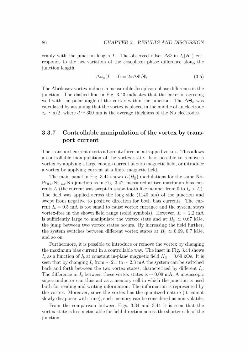
86 CHAPTER 3. RESULTS AND DISCUSSION
erably with the junction length L. The observed offset ∆Φ in Ic(H||) cor-responds to the net variation of the Josephson phase difference along thejunction length
∆φv(L− 0) = 2π∆Φ/Φ0. (3.5)
The Abrikosov vortex induces a measurable Josephson phase difference in thejunction. The dashed line in Fig. 3.43 indicates that the latter is agreeingwell with the polar angle of the vortex within the junction. The ∆Θv wascalculated by assuming that the vortex is placed in the middle of an electrodezv ≃ d/2, where d ≃ 300 nm is the average thickness of the Nb electrodes.
3.3.7 Controllable manipulation of the vortex by trans-port current
The transport current exerts a Lorentz force on a trapped vortex. This allowsa controllable manipulation of the vortex state. It is possible to remove avortex by applying a large enough current at zero magnetic field, or introducea vortex by applying current at a finite magnetic field.
The main panel in Fig. 3.44 shows Ic(H||) modulations for the same Nb-Pt0.46Ni0.54-Nb junction as in Fig. 3.42, measured at two maximum bias cur-rents Ib (the current was swept in a saw-tooth like manner from 0 to Ib > Ic).The field was applied across the long side (1140 nm) of the junction andswept from negative to positive direction for both bias currents. The cur-rent Ib = 0.5 mA is too small to cause vortex entrance and the system staysvortex-free in the shown field range (solid symbols). However, Ib = 2.2 mAis sufficiently large to manipulate the vortex state and at H|| ≃ 0.67 kOe,the jump between two vortex states occurs. By increasing the field further,the system switches between different vortex states at H|| ≃ 0.69, 0.7 kOe,and so on.
Furthermore, it is possible to introduce or remove the vortex by changingthe maximum bias current in a controllable way. The inset in Fig. 3.44 showsIc as a function of Ib at constant in-plane magnetic field H|| = 0.69 kOe. It isseen that by changing Ib from ∼ 2.1 to ∼ 2.3 mA the system can be switchedback and forth between the two vortex states, characterized by different Ic.The difference in Ic between these vortex states is ∼ 0.09 mA. A mesoscopicsuperconductor can thus act as a memory cell in which the junction is usedboth for reading and writing information. The information is represented bythe vortex. Moreover, since the vortex has the quantized nature (it cannotslowly disappear with time), such memory can be considered as non-volatile.
From the comparison between Figs. 3.34 and 3.44 it is seen that thevortex state is less metastable for field direction across the shorter side of thejunction.

3.3. MESOSCOPIC JOSEPHSON JUNCTIONS 87
0.6 0.70.0
0.1
0.2
0.3
0.4
2.2 2.30.05
0.10
0.15 H=0.69 kOe
H (kOe)
I c (m
A)
Ib=2.2 mA I
b (mA)
I c (m
A)
Ib=0.5 mA
Fig. 3.44. Main panel shows Ic(H||) modulations of the Nb-Pt0.46Ni0.54-Nb junction forbias currents of 0.5 mA (full squares) and 2.2 mA (open circles) at T = 1.83 K. The fieldwas applied across the junction side of 1140 nm. For Ib = 2.2 mA, the system switchesbetween different vortex states upon increasing the field. For Ib = 0.5 mA, the systemremains in the vortex-free state over the whole field range shown here. Inset shows Ic vsIb for the same Josephson junction at T = 1.83 K and at constant H|| ≃ 0.69 kOe. Bychanging the bias current from ∼ 2.1 to ∼ 2.3 mA the system can be brought between twovortex states with the difference in Ic between these vortex states ∼ 0.09 mA.
3.3.8 Discussion of unsustainable scenarios of phaseshifts in Josephson junctions
As it was mentioned in sections 1.3 and 3.3.6, the measured phase shiftsin Josephson junctions can be described in terms of phase rotation inducedby an Abrikosov vortex. It should be noticed, however, that the questionwhether a distant Abrikosov vortex gives rise to a Josephson junction phaseshift or not is non-trivial. The reason is the gauge-invariance principle whichallows adding a gradient of arbitrary scalar function to the phase. This meansthat only loop integrals of gauge fields are significant, while line integrals arenon-integrable and should not be measurable. For example, we can only saythat the total phase shift around the vortex is 2π, but cannot say that thephase difference from the left to the right side of the vortex is π. In thissection some other scenarios which may contribute to the observable phaseshifts in Josephson junctions will be discussed.
First of all, the possibility to control the induced flux offset ∆Φ in the de-tector junction solely by the transport current (see subsection 3.3.7) clearlydemonstrates that the observed phenomenon is caused by the Abrikosov vor-
88 CHAPTER 3. RESULTS AND DISCUSSION
tex. However, the vortex can affect Ic(Φ) patterns in a different ways:
Direct penetration of the full vortex flux Φ0 into the junction. In the studiedstructures, the Abrikosov vortices were oriented strictly parallel to the junc-tion interface and never cross the junction area. In particular, such crossingis impossible for the planar junctions because of the two-dimensional junc-tion geometry. The mesoscopic sizes of the Nb-PtNi-Nb junctions help toconfine the vortex in the middle of the electrode, parallel to the junctionplane, and allow detection of Ic in very strong magnetic fields up to 20 kOe,which further helps to align the vortex.
Direct field of a vortex. The magnetic field from a vortex can penetratein to a bulk superconductor over the distance λ (see section 1.3), which is∼ 150 nm for Nb. If this field would stretch into the junction area, it wouldgenerate some Josephson phase shift according to equation (1.14). However,this field must have the same sign as the applied field, while in experiment itis always observed that the effective trapped flux is opposite to the appliedfield. Moreover, when the vortex traps were used, the distance to the junctionwas always larger than λ. Thus, the phenomenon cannot be due to directfield from the vortex.
Effect of magnetic barrier . In some cases barrier layers in our junctionscontain Ni and are ferromagnetic at low T. Junctions with non-magneticbarriers: planar junctions with pure Cu barrier and mesoscopic junctionswith pure Pt barrier were also studied. Similar phenomena were observedfor junctions with both magnetic and non-magnetic barriers. Data for twonon-magnetic Nb-Pt-Nb junctions are explicitly shown in Fig. 3.43 (greencircles and a down triangle) and clearly follow the same trend. Therefore,the phenomenon as such is not caused by the magnetism in the barrier. Themagnetic barrier was used to reduce the critical current to a comfortablerange below about 1 mA. The observed offset of the Fraunhofer pattern iscertainly not related to the magnetism of the barrier because a ferromagnetwould be magnetized in the direction of the applied field, in contrast with theexperimental observations. There is no reason for the magnetic moment ofa ferromagnet to induce a quantized Φ0/2 flux contribution in the junctioneither. The possibility to manipulate ∆Φ by a transport current clearlyindicates that it is caused by vortices in electrodes rather than magnetism inthe barrier.
Vortex current. It can be shown [106] that the contribution from the vortexcurrent may be significant leading to a flux shift in Ic(Φ) in the observeddirection. However, it depends crucially on a number of parameters: zv, λ,d, L. Since the same behavior is obsereved for two very different types ofjunctions with substantially different parameters, one can conclude that theobserved direct correspondence of the induced Josephson phase shift to thepolar angle of the vortex cannot be explained by the vortex current alone.

3.3. MESOSCOPIC JOSEPHSON JUNCTIONS 89
Effect of stray fields : Stray fields from a vortex returning back through thejunction area generate field in the direction opposite to the vortex field andwould give rise to a flux shift in Ic(Φ), similar to the vortex current con-tribution. In fact, there is a well known fundamental connection betweenthe magnetic field outside the superconductor and the surface current inthe superconductor. Therefore, effects of the vortex stray field and the sur-face current at the junction interface are identical [follow for example thetransition from equation (1.10) to equation (1.14)]. Discussion in terms ofstray field lines from the vortex closing through the junction area is perhapsmore illustrative because it shows more clearly the nontrivial behavior of thetrapped flux in the junction. Indeed, in the classical case, i.e., in the ab-sence of Josephson effect in the junction Ic = 0, the stray field distributionshould be governed by simple magnetostatics, which minimizes the magneticfield energy outside the superconductor. In this case only a small portion ofthe total flux should go through the junction because field focusing in thenarrow slit costs extra energy. To the contrary, it is observed that a half ofthe flux ∆Φ ≃ Φ0/2 is going through the junction for long enough junctions.Such quantization is not expected for the magnetostatic stray field. Mostclearly the non-magnetostatic behavior of the trapped flux is demonstratedby the experiment with the stray field drain. As seen from Fig. 3.36(b),the drain opens an additional area for returning the stray field, which ismore than twenty times larger than the area of the junction slit. It is clearthat this should dramatically reduce the magnetostatic flux in the junctionslit. However, experimental data in Fig. 3.37 show that this is not the case.Apparently, a magnetostatic stray field alone cannot explain the observedphenomenon.

90 CHAPTER 3. RESULTS AND DISCUSSION

Summary
During this work, two types of mesoscopic S-F-S and S-N-S Josephson junc-tions were fabricated using Focused Ion Beam (FIB) milling: nanoscale junc-tions of the “overlap” type and planar junctions of the “variable thickness”type. A Pt1−xNix alloy with a Ni concentration ranging between 0 and 67at.%, Cu or a Cu0.47Ni0.53 alloy were used as a junction barrier. The FIBallows to fabricate the Josephson junctions with a size down to 70× 80 nm2.The small size of the junction allows to use conventional measurement tech-niques due to sufficiently high junction resistance (Rn & 0.1Ω) and facilitatedmono-domain structure of the F layer.
To study the chemical composition of the deposited Pt1−xNix thin films,energy dispersive X-ray spectroscopy (EDS) was used. To eliminate possibleerrors during the EDS characterization caused by the secondary fluorescenceand the errors in the quantitative analysis, the results were analyzed depend-ing on the electron beam energy and incident angle. To completely eliminatethe possible effect of the substrate material the EDS characterization wasalso performed on free standing Pt0.67Ni0.33 flakes. Various complications forEDS on thin films were discussed. It was found that the conventional quan-titative correction for the bulk specimen analysis cannot be applied to thethin film when using intermediate electron beam energies. The correctionprocedure, which was used during this work, seems to work properly for theelectron beam energies of 15 and 30 keV. Thus, it is advisable to use highelectron beam energies for chemical analysis of thin films.
To characterize the ferromagnetic properties of Pt1−xNix thin films, theHall effect in the films with Ni concentrations of 13, 27, 40 and 67 at.% andwith thicknesses ∼ 50− 60 nm was studied. Measurements were carried outover a temperature range from 1.8 K to 300 K, fields up to ±10 T, and atdifferent angles between the field and the film surface.
It is found that films with sub-critical Ni concentration of 13 and 27 at.%are superparamagnetic at low T and exhibit perpendicular magneticanisotropy. Films with over-critical Ni concentration of 67 at.% are fer-romagnetic with parallel anisotropy. At the critical Ni concentration of40 at.% the films demonstrate canted magnetization with the easy axis rotat-ing as a function of temperature. The magnetism appears via two crossoversparamagnetic-superparamagnetic-ferromagnetic, and the extraordinary Halleffect changes sign at low T while the ordinary Hall effect does not.
91
92 CHAPTER 3. RESULTS AND DISCUSSION
The I − V characteristics of the measured junctions are well describedby the RCSJ model. The studied junctions with different Ni concentrationsin the barrier layer are characterized by the good quality of the measuredFraunhofer patterns. This serves as the evidence for uniformity of the junc-tion properties and monodomain structure of the ferromagnetic layer.
The critical current density of the Nb-PtNi-Nb junctions has a strong tem-perature dependence and becomes exponentially dependent on the temper-ature for high Ni concentrations. The observed non-monotonic dependenceof the critical current density on the Ni concentration can be attributed toswitching from the conventional 0 state into the π state.
The fabricated junctions were used as phase sensitive detectors for theanalysis of vortex states in mesoscopic superconductors. The position of thevortex in the “overlap” type junctions were controlled by a suitable samplegeometry. In order to control the position of the vortex near the planarjunction a small hole with a diameter of ∼ 30 nm working as a vortex trapwas made. It is found that the vortex induces a different phase shift in aJosephson junction which is equal to the polar angle of the vortex. This inturn results in different flux shifts in the Ic(H∥) modulation, depending onthe position of the vortex. The flux in the junction shows an unusual Φ0/2quantization when the vortex is close to the junction.
The vortices were manipulated either by an external magnetic field or bya bias current through the junction. By changing the junction bias currentat constant magnetic field it is possible to toggle the system between twoconsecutive vortex states which are characterized by different Ic. A meso-scopic superconductor thus acts as a memory cell. The neighboring junctionis used for reading the information since the change of Ic indicates that thevortex appears or disappears in the superconductor. By applying the currentthrough the junction the vortex is thus introduced in the superconductor orremoved in such a way that information is written or erased.

Conclusions
A collapse of the switching current fluctuations with increasing temperaturewas observed in moderately damped Josephson junctions. Such an anticor-relation with a temperature was explained by interplay of two conflictingconsequences of thermal fluctuations, which, on one hand, assist in prema-ture switching to the resistive state and, on the other hand, help in retrappingback to the superconducting state.
A PtNi alloy was employed for S-F-S Josephson junctions. The fabricatedjunctions are characterized by the good uniformity of the junction propertiesand the monodomain structure of the ferromagnetic layer. Therefore, suchjunctions may be promising for hybrid S-F spin-valve devices which requirea small, mono-domain ferromagnetic barrier.
Magnetic properties of PtNi thin films were studied. Unusual sign changeof the extraordinary Hall effect was observed at the critical concentrationindicating a reconstruction of the Fermi surface and possibly a quantumphase transition.
It is found that introduction of a single Abrikosov vortex leads to a con-trollable and reversible switching of a conventional 0 – Josephson junctioninto the 0 – π state. The vortex may hence act as a tunable “phase battery”for quantum electronics.
93

94 CHAPTER 3. RESULTS AND DISCUSSION

Acknowledgments
First of all, I would like to thank my supervisor Professor Vladimir Krasnovfor his support, advice and guidance during my work. Special thanks toAndreas Rydh for all his brilliant solutions of measurement problems and forthe fruitful discussions.
Many thanks to Henrik Frederiksen and Alexey Pavolotsky from ChalmersUniversity of Technology for their help with sample fabrication. I am thank-ful to V. A. Oboznov and V. V. Ryazanov from Institute of Solid StatePhysics in Chernogolovka for providing me with the CuNi-Nb bilayers. I amgrateful to Kjell Jansson and Osamu Terasaki from Arrhenius Laboratory fortheir help with sample characterization.
I am grateful to all present and former members of Experimental Con-densed Matter Physics group for their help and interesting discussions. Thankyou Holger Motzkau for proofreading this thesis and providing useful com-ments.
I would also like to thank the KTH group of Nanostructure Physics forfruitfull collaboration. I am grateful to the staff of the AlbaNova Nanofabri-cation lab and the staff of the Core facility in Nanotechnology at StockholmUniversity for keeping the clean room facilities running smoothly.
On a personal level, my very special and enormous thanks go to myparents and to my brother Igor for all their unlimited love, support andencouragement throughout my life.
Finally, I would like to thank my lovely wife Oresta. There are no suchwords to express all my gratitude for all your love, help, support and under-standing.
95

96 CHAPTER 3. RESULTS AND DISCUSSION

Bibliography
[1] Y. Imry, Introduction to mesoscopic physics, Oxford University Press(2002).
[2] Akira Tonomura, The quantum world unveiled by electron waves, WorldScientific (1998).
[3] K. K. Likharev, Dynamics of Josephson junctions and circuits, Gordonand Breach Science Publishers (1986).
[4] Bascom S. Deaver, Jr. and William M. Fairbank, Phys. Rev. Lett. 7, 43(1961).
[5] R. Doll and M. Nabauer, Phys. Rev. Lett. 7, 51 (1961).
[6] B. D. Josephson, Phys. Lett. 1, 251 (1962).
[7] P. W. Anderson and J. M. Rowell, Phys. Rev. Lett. 10, 230 (1963).
[8] K. K. Likharev, Rev. Mod. Phys. 51, 101 (1979).
[9] A. I. Buzdin, Rev. Mod. Phys. 77, 935 (2005).
[10] L. Bulaevskii, V. Kuzii, and A. Sobyanin, JETP Lett. 25, 7 (1977).
[11] V. V. Ryazanov, V. A. Oboznov, A. Yu. Rusanov, A. V. Veretennikov,A. A. Golubov, and J. Aarts, Phys. Rev. Lett. 86, 2427 (2001).
[12] T. Kontos, M. Aprili, J. Lesueur, F. Genet, B. Stephanidis, and R.Boursier, Phys. Rev. Lett. 89, 137007 (2002).
[13] M. Weides, M. Kemmler, E. Goldobin, D. Koelle, R. Kleiner, and H.Kohlstedt, Appl. Phys. Lett. 89, 122511 (2006).
[14] Y. Blum, A. Tsukernik, M. Karpovski, and A. Palevski, Phys. Rev. Lett.89, 187004 (2002).
[15] J. W. A. Robinson, S. Piano, G. Burnell, C. Bell, and M. G. Blamire,Phys. Rev. Lett. 97, 177003 (2006).
97
98 BIBLIOGRAPHY
[16] R. S. Keizer, S. T. B. Goennenwein, T. M. Klapwijk, G. Miao, G. Xiao,and A. Gupta, Nature (London) 439, 825 (2006).
[17] T. Yokoyama, Y. Tanaka, and A. A. Golubov, Phys. Rev. B 75, 134510(2007).
[18] F. S. Berget, A. F. Volkov, and K. B. Efetov, Phys. Rev. Lett. 86, 4096(2001).
[19] G. Blatter, V. B. Geshkenbein, and L. B. Ioffe, Phys. Rev. B 63, 174511(2001); E. Terzioglu and M. R. Beasley, IEEE Trans. Appl. Supercond.8, 48 (1998); A. V. Ustinov and V. K. Kaplunenko, J. Appl. Phys. 94,5405 (2003).
[20] A. K. Feofanov, V. A. Oboznov, V. V. Bolginov, J. Lisenfeld, S. Po-letto, V. V. Ryazanov, A. N. Rossolenko, M. Khabipov, D. Balashov, A.B. Zorin, P. N. Dmitriev, V. P. Koshelets, and A. V. Ustinov, NaturePhysics 6, 593 (2010).
[21] I. Zutic, J. Fabian, and S. Das Sarma, Rev. Mod. Phys. 76, 323 (2004).
[22] Daniel Huertas-Hernando, Yu. V. Nazarov, and W. Belzig, Phys. Rev.Lett. 88, 047003 (2002).
[23] P. Grunberg, R. Schreiber, Y. Pang, M. B. Brodsky, and H. Sowers,Phys. Rev. Lett. 57, 2442 (1986); M. N. Baibich , J. M. Broto, A. Fert,F. Nguyen Van Dau, F. Petroff, P. Eitenne, G. Creuzet, A. Friederich,and J. Chazelas, Phys. Rev. Lett. 61, 2472 (1988).
[24] W. L. McMillan, Phys. Rev. 175, 537 (1968).
[25] M. J. Besnus, and A. Herr, Phys. Lett. A 39, 83 (1972).
[26] J. Beille, D. Bloch, and M. J. Besnus, J. Phys. F 4, 1275 (1974).
[27] Uday Kumar, P. K. Mukhopadhyay, Biplab Sanyal, Olle Eriksson, PerNordblad, Durga Paudyal, Kartick Tarafder, and Abhijit Mookerjee,Phys. Rev. B 74, 064401 (2006).
[28] Y. Jugnet, J. C. Bertolini, J. Massardier, B. Tardy, T. M. Duc, and J.C. Vedrine, Surf. Sci. 107, L320 (1981).
[29] J. Sedlacek, L. Hilaire, P. Legare, and G. Maire, Surf. Sci. 115, 541(1982).
[30] A. A. Golubov, M. Yu. Kupriyanov and E. Il’ichev, Rev. Mod. Phys.76, 411 (2004).
[31] A. Buzdin and I. Baladie, Phys. Rev. B 67, 184519 (2003).

BIBLIOGRAPHY 99
[32] A. F. Andreev, Sov. Phys. JETP 19, 1228 (1964).
[33] V. V. Schmidt, The Physics of Superconductors: Introduction to Funda-mentals and Applications, Springer-Verlag (1997).
[34] M. Tinkham, Introduction to Superconductivity, Dover Publications, Inc.(2004).
[35] V. M. Krasnov and D. Winkler, Phys. Rev. B 56, 9106 (1997).
[36] Y. Aharonov and D. Bohm, Phys. Rev. 115, 485 (1959).
[37] E.du Tremolet de Lacheisserie, D. Gignoux, and M. Schlenker, Mag-netism: Fundamentals, Materials and Applications, Springer (2005).
[38] Colin M. Hurd, The Hall Effect in Metals and Alloys, Plenum Press(1972).
[39] Emerson M. Pugh and Norman Rostoker, Rev. Mod. Phys. 25, 151(1953).
[40] Naoto Nagaosa, Jairo Sinova, Shigeki Onoda, A. H. MacDonald, and N.P. Ong, Rev. Mod. Phys. 82, 1539 (2010).
[41] J. Smit, Physica (Amsterdam) 21, 877 (1955).
[42] J. Smit, Physica (Amsterdam) 24, 39 (1958).
[43] L. Berger, Phys. Rev. B 2, 4559 (1970).
[44] M. V. Berry, Proc. R. Soc. London 392, 45 (1984).
[45] N. P. Ong and W.-L. Lee, in Foundations of Quantum Mechanicsin the Light of New Technology (Proceedings of ISQM Tokyo 2005),edited by S. Ishioka and K. Fujikawa, World Scientific, 121 (2006)(http://arxiv.org/abs/cond-mat/0508236).
[46] K. Okamoto, T. Shirahawa, S. Matsushita, and Y. Sakurai, IEEE Trans.Magn. MAG-10, 799 (1974).
[47] T. R. McGuire, R. J. Gambino, and R. C. Taylor, IEEE Trans. Magn.MAG-13, 1598 (1977).
[48] C. L. Canedy, G. Q. Gong, J. Q. Wang, and G. Xiao, J. Appl. Phys. 79,6126 (1996).
[49] G. X. Miao and G. Xiao, Appl. Phys. Lett. 85, 73 (2004).
[50] M. Watanabe and T. Masumoto, Thin Solid Films 405, 92 (2002)

100 BIBLIOGRAPHY
[51] S. Foner, Rev. Sci. Instrum. 30, 548 (1959).
[52] A. H. Miklich, J. J. Kingston, F. C. Wellstood, J. Clarke, M. S. Col-clough, K. Char, and G. Zaharchuk, Appl. Phys. Lett. 59, 988 (1991).
[53] D. Budker and M. Romalis, Nature Physics 3, 227 (2007).
[54] The Hall Effect and Its Applications, edited by C. L. Chien and C. R.Westgate, Plenum, New York (1980).
[55] A. Gerber, A. Milner, M. Karpovsky, B. Lemke, H.-U. Habermeier, J.Tuaillon-Combes, M. Negrier, O. Boisron, P. Melinon, and A. Perez, J.Magn. Magn. Mater. 242-245, 90 (2002).
[56] R. Allenspach and A. Bischof, Phys. Rev. Lett. 69, 3385 (1992).
[57] P. Xhonneux and E. Courtens, Phys. Rev. B 46, 556 (1992).
[58] Z. Q. Qiu, J. Pearson, and S. D. Bader, Phys. Rev. Lett. 70, 1006 (1993);B. Schulz and K. Baberschke, Phys. Rev. B 50, 13467 (1994).
[59] D. Li M. Freitag, J. Pearson, Z. Q. Qiu, and S. D. Bader, Phys. Rev.Lett. 72, 3112 (1994).
[60] D. E. Fowler and J. V. Barth, Phys. Rev. B 53, 5563 (1996).
[61] M.-T. Lin, J. Shen, W. Kuch, H. Jenniches, M. Klaua, C. M. Schneider,and J. Kirschner, Phys. Rev. B 55, 5886 (1996).
[62] C. A. F. Vaz, J. A. C. Bland, and G. Lauhoff, Rep. Prog. Phys. 71,056501 (2008).
[63] I. S. Veshchunov, V. A. Oboznov, A. N. Rossolenko, A. S. Prokofiev, L.Ya. Vinnikov, A. Yu. Rusanov, and D. V. Matveev, JETP Lett 88, 758(2008).
[64] K. Okamoto, J. Appl. Phys. 53, 601 (1982).
[65] K. Okamoto, J. Magn. Magn. Mater. 35, 353 (1983).
[66] K. Okamoto, IEEE Transl. J. Magn. Jpn. 5, 1053 (1990).
[67] C. P. Bean and J. D. Livingston, J. Appl. Phys. 30”, S120 (1959).
[68] C. M. Hurd, Contemp. Phys. 23, 469 (1982).
[69] L. Vila, T. Kimura, and Y. C. Otani, Phys. Rev. Lett. 99, 226604 (2007).
[70] G. Y. Guo, S. Murakami, T.-W. Chen, and N. Nagaosa, Phys. Rev. Lett.100, 096401 (2008).
BIBLIOGRAPHY 101
[71] C. E. Dahmani, M. C. Cadeville, J. M. Sanchez, and J. L. Moran-Lopez,Phys. Rev. Lett. 55, 1208 (1985).
[72] A. V. Ruban, I. A. Abrikosov, and H. L. Skriver, Phys. Rev. B 51, 12958(1995).
[73] W. Olovsson, C. Goransson, L. V. Pourovskii, B. Johansson, and I. A.Abrikosov, Phys. Rev. B 72, 064203 (2005).
[74] H. L. Alberts, J. Beille, D. Bloch, and E. P. Wohlfarth, Phys. Rev. B 9,2233 (1974).
[75] Uday Kumar, K. G. Padmalekha, P. K. Mukhopadhyay, Durga Paudyal,and Abhijit Mookerjee, Journal of Magnetism and Magnetic Materials292, 234 (2005).
[76] R. E. Parra and J. W. Cable, Phys. Rev. B 21, 5494 (1980).
[77] C. E. Dahmani, M. C. Cadeville, J.M. Sanchez, and J.L. Moran-Lopez,Phys. Rev. Lett. 55, 1208 (1985).
[78] E. A. Demler, G. B. Arnold and M. R. Beasley, Phys. Rev. B 55, 15174(1997).
[79] G. Eilenberger, Z. Phys. 214, 195 (1968).
[80] L. Usadel, Phys. Rev. Lett. 25, 507 (1970).
[81] A. I. Buzdin, L. N. Bulaevskii, and S. V. Panyukov, JETP Lett. 35, 178(1982).
[82] A. I. Buzdin, and M. Y. Kuprianov, JETP Lett. 53, 321 (1991).
[83] Yutaka Sato, Takayuki Ishibashi, Keisuke Obara, Shunji Ichida, Yoshi-taka Morishita, and Katsuaki Sato, Jpn. J. Appl. Phys. 46, L297 (2007).
[84] C. Bell, G. Burnell, D-J. Kang, R. H. Hadfield, M. J. Kappers, and M.G. Blamire, Nanotechnology 14, 630 (2003).
[85] D. Nakada, K. K. Berggren, E. Macedo, V. Liberman, and T. P. Orlando,IEEE Transactions on Applied Superconductivity 13, 111 (2003).
[86] T. M. Phung et al., X-Ray Spectrom. 37, 608 (2008).
[87] M. Takakura, H. Takahashi and T. Okumura, JEOL News 33, 15 (1998).
[88] Jean-Louis Pouchou and Francoise Pichoir, Quantitative analysis of ho-mogeneous or stratified microvolumes applying the model PAP, pages31-75 of Electron Probe Quantitation edited by K. F. J. Heinrich andDate E. Newbury, Plenum (1991).

102 BIBLIOGRAPHY
[89] G. F. Bastin and H. J. M. Heijligers, X-Ray Spectrom. 29, 212 (2000).
[90] V. N. Matveev, V. I. Levashov, O. V. Kononenko, and A. N. Chaika,Russian Microelectronics 35, 392 (2006).
[91] A. Gerber, A. Milner, M. Karpovsky, B. Lemke, H.-U. Habermeier, J.Tuaillon-Combes, M. Negrier, O. Boisron, P. Melinon, and A. Perez, J.Magn. Magn. Mater. 242-245, 90 (2002).
[92] V. T. Volkov, V. I. Levashov, V. N. Matveev, and V. A. Berezin, Appl.Phys. Lett. 91, 262511 (2007).
[93] D. G. Stinson, A. C. Palumbo, B. Brandt, and M. Berger, J. Appl. Phys.61, 3816 (1987).
[94] Z. Q. Lu, G. Pan, and Y. K. Zheng, J. Appl. Phys. 91, 2161 (2002).
[95] Z. Q. Lu, G. Pan, W. Y. Lai, D. J. Mapps, and W. W. Clegg, J. Magn.Magn. Mater. 242-245, 525 (2002).
[96] B. A. Aronzon, A. B. Granovskii, S. N. Nikolaev,D. Yu. Kovalev, N. S.Perov, and V. V. Ryl’kov, Phys. Solid State, 46, 1482 (2004).
[97] G. Burnell, E. J. Tarte, D.-J. Kang, R. H.Hadfield, and M. G. Blamire,Physica C 241, 241 (2002).
[98] V. M. Krasnov, Physica C 252, 319 (1995).
[99] A. S. Vasenko, A. A. Golubov, M. Yu. Kupriyanov, and M. Weides,Phys. Rev. B 77 134507 (2008).
[100] A. K. Geim, S. V. Dubonos, J. J. Palacios, I. V. Grigorieva, M. Henini,and J. J. Schermer, Phys. Rev. Lett. 85, 1528 (2000).
[101] A. Kanda, B. J. Baelus, F. M. Peeters, K. Kadowaki, and Y. Ootuka,Phys. Rev. Lett. 93, 257002 (2004).
[102] G. Karapetrov, J. Fedor, M. Iavarone, M. T. Marshall, and R. Divan,Appl. Phys. Lett. 87, 162515 (2005).
[103] T. Nishio, S. Okayasu, J. Suzuki, and K. Kadowaki, Physica C 412-414, 379 (2004).
[104] A. Volodin, K. Temst, C. V. Haesendonck, and Y. Bruynseraede, Phys-ica C 332, 156 (2000).
[105] H. J. Zhao, V. R. Misko, F. M. Peeters, V. Oboznov, S. V. Dubonos,and I.V. Grigorieva, Phys. Rev. B 78, 104517 (2008).
[106] See supplementary material to the appended paper V athttp://link.aps.org/supplemental/10.1103/PhysRevLett.104.227003.
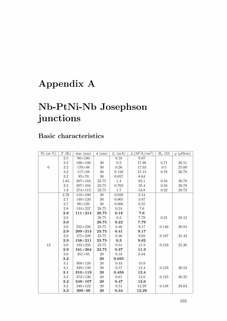
Appendix A
Nb-PtNi-Nb Josephsonjunctions
Basic characteristics
Ni (at.%) T (K) size (nm) d (nm) Ic (mA) Jc(105A/cm2) Rn (Ω) ρ (µΩcm)
2.5 90×180 0.16 9.873.2 106×106 30 0.2 17.86 0.71 26.51
0 3.2 170×88 30 0.26 17.33 0.5 25.003.2 117×88 30 0.156 15.15 0.78 26.783.2 95×70 30 0.057 8.641.65 207×104 23.75 1.4 65.1 0.34 30.783.2 207×104 23.75 0.762 35.4 0.34 30.781.8 274×113 23.75 1.7 54.8 0.22 28.722.76 110×100 30 0.028 2.542.7 140×120 30 0.065 3.872.7 90×120 30 0.006 0.552.8 134×237 28.75 0.24 7.62.8 111×214 28.75 0.18 7.62.8 28.75 0.3 7.79 0.21 28.123.0 28.75 0.22 7.793.0 222×226 23.75 0.46 9.17 0.146 30.842.9 209×213 23.75 0.41 9.173.0 175×228 23.75 0.36 9.02 0.187 31.422.9 158×211 23.75 0.3 9.02
13 3.0 192×235 23.75 0.51 11.3 0.133 25.262.9 161×204 23.75 0.37 11.33.0 351×85 20 0.18 6.043.2 20 0.0353.1 308×128 20 0.43 10.93.1 330×139 20 0.57 12.4 0.133 30.523.1 310×119 20 0.456 12.43.2 372×130 20 0.61 12.6 0.125 30.253.2 349×107 20 0.47 12.63.2 340×122 20 0.51 12.29 0.138 28.633.2 308×90 20 0.34 12.29
103

104 APPENDIX A. Nb-PtNi-Nb JOSEPHSON JUNCTIONS
Ni (at.%) T (K) size (nm) d (nm) Ic (mA) Jc(105A/cm2) Rn (Ω) ρ (µΩcm)
2.9 144×197 20 0.23 8.132.9 144×229 20 0.3 9.123.1 319×106 30 0.12 3.55 0.237 26.703.08 30 0.024 3.553.1 266×128 30 0.13 3.82 0.228 25.843.2 30 0.043 3.82
20 3.1 319×117 30 0.18 4.83 0.181 22.503.3 280×95 30 0.129 4.833.0 287×106 25 0.12 3.95 0.302 36.723.0 277×128 25 0.155 4.37 0.248 35.223.0 170×106 25 0.08 4.44 0.462 33.263.0 287×106 25 0.125 4.11 0.307 37.333.0 319×64 25 0.08 3.92 0.390 31.823.1 266×181 25 0.25 5.23.1 193×266 30 0.104 2.03 0.203 34.713.1 167×266 30 0.095 2.14 0.218 32.263.1 140×256 30 0.073 2.04 0.278 33.173.2 210×120 20 0.1015 4.03 0.415 52.293.2 210×170 20 0.157 4.4 0.293 52.303.2 212×90 20 0.072 3.77 0.53 50.61
27 3.2 210×190 20 0.179 4.49 0.245 48.883.2 202×140 20 0.120 4.24 0.36 50.943.2 175×180 20 0.137 4.35 0.335 52.763.08 158×149 25 0.0615 2.62 0.375 35.253.08 175×123 25 0.074 3.44 0.33 28.383.2 175×140 20 0.13 5.31 0.3 36.753.2 255×96 20 0.136 5.55 0.32 39.203.0 300×165 30 0.14 2.83 2.0 330.003.0 280×180 30 0.0075 0.149 1.03 173.043.0 260×110 30 0.0183 0.64 2.2 209.73
40 2.8 640×225 30 0.11 0.76 0.3 144.002.18 630×230 25 0.16 1.1 0.05 29.002.19 770×320 25 2.07 8.4 0.22 216.832.97 770×320 25 0.73 2.96 0.22 216.833.17 770×320 25 0.52 2.11 0.22 216.831.8 800×225 20 0.063 0.35 0.05 45.002.2 800×225 20 0.048 0.267 0.05 45.003.0 800×225 20 0.028 0.156 0.05 45.003.2 800×225 20 0.025 0.139 0.05 45.00
54 1.8 1140×230 20 2.1 8.0 0.12 157.322.2 1140×230 20 1.6 6.1 0.12 157.323.0 1140×230 20 0.8 3.05 0.12 157.323.2 1140×230 20 0.67 2.55 0.12 157.321.8 1140×380 20 0.092 0.21 0.022 47.651.8 1200×300 20 3.49 9.69 0.09 162.002.2 1200×300 20 2.87 7.98 0.09 162.00
60 3.0 1200×300 20 1.48 4.12 0.09 162.003.2 1200×300 20 1.17 3.26 0.09 162.001.8 1050×420 20 0.136 0.308 0.025 55.102.2 1050×420 20 0.1 0.227 0.025 55.10

105
Ni (at.%) T (K) size (nm) d (nm) Ic (mA) Jc(105A/cm2) Rn (Ω) ρ (µΩcm)
60 3.0 1050×420 20 0.062 0.141 0.025 55.103.2 1050×420 20 0.058 0.131 0.025 55.102.0 190×350 20 0.16 53.202.0 120×350 20 0.25 52.50
67 2.0 182×290 20 0.20 52.782.0 180×410 20 0.16 59.002.0 160×490 20 0.135 52.9
Junctions described by the bold type were anodized prior the measure-ments (see subsection 2.1.4). Each anodized junction in the table followsthe same junction characterized before anodization. The depth of anodiza-tion was estimated by assuming that the critical current density remains thesame for a junction before and after anodization. Then by measuring thecritical current after anodization, and taking into account the value of criti-cal current density before anodization, the effective area of the junction wasestimated.

106 APPENDIX A. Nb-PtNi-Nb JOSEPHSON JUNCTIONS

Appended papers
107
Copyright © 2022 FDOKUMEN