HIGH-TC SUPERCONDUCTIVITY TUNNELING PHENOMENA
205
Second International Symposium •;-"' HIGH-T C SUPERCONDUCTIVITY TUNNELING PHENOMENA Sept.3-6, 1994 Donetsk Slavyanogorsk UKRAINE
-
Upload
khangminh22 -
Category
Documents
-
view
1 -
download
0
Transcript of HIGH-TC SUPERCONDUCTIVITY TUNNELING PHENOMENA

SecondInternationalSymposium
• ; - " '
HIGH-TC
SUPERCONDUCTIVITYTUNNELINGPHENOMENA
Sept.3-6, 1994
DonetskSlavyanogorsk
UKRAINE

W/i-6 ' l - j> t-V-.-b UA9600431
Proceedings of the IS-HTS-TP'942nd International Symposium on
HIGH TEMPERATURESUPERCONDUCTIVITY
and TUNNELINGPHENOMENA
September 3-6 1994,Slavyanogorsk (Donetsk), Ukraine
EditorVladimir M.Svistunov
Donetsk - 1995
SPONSORS
National Academy of Sciences of UkraineState Committee for Science and Technology of UkraineJapan Society for Promotion of ScienceScientific Council of the National Program of Russia on" High-Temperature Superconductivity"
SYMPOSIUM CO-CHAIRMEN
V.G.Baryakhtar Vice-President of the NationalAcademy of Sciences of Ukraine
S.M.Ryabchenko Chairman of the State Committee ofScience and Technology of Ukraine
E.A.Zavadskii Director of A.Galkin DonetskPhysico-Technical Institute
SYMPOSIUM CHAIRMEN
V.M.Svistunov
A.Galkin Donetsk Physico-Technical InstituteNational Academy of Sciences of Ukraine72 Str. R.Luxemburg, Donetsk, 340114, UkraineFAX: (0622) 55-01-27E-mail: svistuno @, sts.dipt.donetsk.ua
C A.Galkin Donetsk Physico-Technical InstituteUkraine National Academy of Sciences, 1995

SYMPOSIUM COMMITTEES
INTERNATIONAL ADVISORY COMMITTEE
A»A.Abrikosov (Argonne)E.Baggio-Saitovich
(Rio de Janeiro)K.Barner (Gottingen)I.Bozovic (Palo Alto)N. A. Chernopleko v
(Moscow)C.W.Chu (Houston)F.de Ja Cruz (Barifeche)I.Iguchi (Tsukuba)V.Z.Kresin (Berkeley)
V.A.Moskalenko(Kishinev)
K.Osamura (Kyoto)Yu.A.Osyp'yan
(Chernogolovka)K, V.RaoH.SzymczakS.TanakaK.TaylorI.K.YansonZ.X.Zhao
(Stockholm)(Warszaw)(Toky6)(Kensigton)(Kharkov)(Beijing)
ORGANIZING COMMITTEE
M.A.Belogolovskii (Donetsk) Yu.V.Medvedev (Donetsk)Secretary Vice-chairman
V.B.Ephimov Yu.V.Melikhov (Donetsk)(Chernogoloyka) A.N.Omelyanchouk
A.M.Grishin (Donelisk) .>- .....vv^^M'̂ K f̂iCQy)..;̂ ^V.P.Kuznetsov (Moscow) E.A.Pashitskii (Kiev) *'V.M.Loktev (Kiev) A.I.Sokolov (Saint Peterburg)
A.A.Zhukov (Moscow)

CEBEPCKOM

CONTENTS
Instead of Preface:Tunnel and direct current transfer in HTCS system. 11
V.M.Svistunov.
I.Tunneling Effect and HTS Mechanisms. 15
Linear Approximation of the Eliashberg equation for obtaing 17
a2(Q) F(Q) from tunneling data. rf$J/ 17R.Aoki, H.Murakami, T.Kita, Y.Nishio, and M.Shirai.
Limitation of the 2A/kTc ratio in a boson theory of high-Tc 21superconductivity: a Monte Carlo study. l~/3->
A.I.D'yachenko.
Feature of the energy gap in YBa2Cu3O7 from break junction , 2 5measurements. hfA V
T.Ekino, T.Minami, and H.Fujii.
Josephson and quasiparticle tunneling for superconductors with ^ 29partial dielectric gapping. i/.?-'>
A.M.Gabovich.
Inelastic electron scattering influence on the strong- coupling oxide 32superconductors. '-[$£
A.M.Gabovich and A.I.Voitenko.
Josephson current in superconducting superstructure. , , , t , OAG.A.Gogadze.
Nonequilibrium states of high Tc YBCO superconductors under ^Qtunnel injection of quasiparticles. >-•'%•?
I.Iguchi, Q.Wang, K.Lee, and K.Yoshida.
Barrier properties of HTSC tunnel junctions. ,, •, fi 44A.I.Khachaturov, M.A.Belogolovskii.

Quantum- and subquantum conductance in SB contacts • A 49J.M.Krans, I.K.Yanson and J.M.van Ruitenbeek
Common features in Josephson self-radiation and Shapiro steps for 53various HTSC junctions. /,/Y/
K.Lee and I.Iguchi.
A microscopic constriction in the superconducting state. 57/ p , /•• A
CJ.Muller, B.J.Vleeming, M.C.Koops and ? r/R.de Brayn Ouboter.
Anisotropyof point-contact spectra of URu2Si2 in normal state. 61Yu.G.Naidyuk, O.E.Kvitnitskya, I.K.Yanson, A.Nowack, "'A.A.Menovsky.
Transparency of atom-sized superconducting junctions. /.V"" ^N.van der Post, E.T.Peters, I.K.Yanson andJ.M.van Ruitenbeek.
On the possible origin of gap smearing in the metaloxide ,__ 66point-contact junctions. ^ ~>
Yu.F.Revenko, D.N.Afanassyev.
The spectral function of electron-boson interactionsof BjSrCaCuO metaloxide.
Yu.F.Revenko, D.N.Afanassyev, V.D.Okunev, I.Iguchi,V.M.Svistunov.
The spectroscopy of 1:2:3-crystal near-surface layer. / / •>' ?*>V.V.Rumyantsev and E.Ya.Shtaerman.
Self energy effects in the normal state tunneling conductivity of 80metal oxides.
V.M.Svistunov, I.Iguchi, K.Lee, AJ.Khachaturov, ? 7 <<M.A.Belogolovskii and D.N.Afanassyev.
Effective interactions and charge ordering in the model with 84local anharmonicity for HTSC systems.
I.V.Stasyuk, A.M.Shvaika and O.D.Danyliv.

Electron tunneling in Bi2223 under high pressure. t-/5~& 88V.Yu.Tarenkov, A.I.D'yachenko, A.V.Abalioshev.
II. Current Transfer. 93
Magnetic-field and dispersion characteristics of Josephson medias. U5i ^L.V.Belevtsov and S.S.Shevchenko.
Giant magnetostriction in textured YBaCuO plates. U'n '• 97V.V.Chabanenko, I.B.Krynetskii, S.Piechota, andH.Szymczak.
Flux instabilities and anisotropy in textured YBaCuO in the strong • r, « 100magnetic fields
V.V.Chabanenko, S.Piechota, H.Szymczak, E.M.Roizenblat,SJ.Ermolina, and N.G.Kisel
Magnetic properties of TmBaCuO7-<5 123 and YBaCuOs 124 103crystals. hr5l/
L.E.Cohen, D.Lacey, G.Perkins, D.Caplin, MingXu,S.X.Dou, S.A.KIestov and V.I.Voronkova.
Determination of irreversibility line and dissipative loss in YBCO 107films. ', 3 5
V.A.Khokhlov and V.F.Drobot'ko.
Double-step behavior of the critical current vs magnetic field in 112a metal ceramic: intergranular fields and relaxation. '-; 5£
A.I.D'yachenko.
Effect of substitution of Hg for Cu on properties of Hg-based 116HSTC. ^
R.V.Lutciv, Yu.N.Myasoedov, M.V.Matviiv, Ya.V.Boiko.
About the role of silver in high temperature reactions on 121Yi Ba2Cu3O7-<5 superconductor ceramic. lff)$
Jorge E.Fiscina, Carlos J.R.Gonzalez Oliver,and Daniel A.Esparza.

Study of current-voltage characteristics in Bi2Sr2CaCu2Ox single 125crystals by pulse method. U5d
S.N.Gordeev, WJahn, A.A.Zhukov, H.Kupfer, A.A.Bush.
Formation mechanism of the (Bi,Pb)-Sr-Ca-Cu-0 system 2223 129phase. //" / Q
M.T.Malachevsky and D.A.Esparza.
The location of two-dimensional superconducting layers in 133
P.M.Mikheenko, V.A.Voloshin, V.V.Babenko, V.Y.Boot'ko,I.M.Reznik, Ya.LYuzhelevskii,
Localized states and superconductivity in BiPbSrCaCuO films. 139V.D.Okunev, N.N.Pafomov, B.I.Perekrestov, I.Iguchi, HK<tV.M.Svistunov.
The microdoping influence on the structure and properties of 144high-Tc YBa2Cu3-xMxOy superconductors. ) / A ̂
V.P.Pashchenko, R.M.Poritski, V.B.Tuytuynnik,O.P.Cherenkov, E.P.Strekalova.
HTSC ceramic current-transport devices. Iffi '4 • 147B.I.Perekrestov, A.V.Vasilenko and J.Leszczynskii
High pressure effect on structure and properties of MeBa2Cu3O7-<5 150(Me = La,Nd,Gd,Sm,Eu) HTSC ceramics. y£C
T.A.Prikhna, V.S.Melnikov, V.E.Moshchil, V.V.Kovylyaev,V.F.Solovyov and P.A.Nagorny.
X-Ray electron spectroscopy study of the electron structure of 154
I.N.Shabanova, S.F.Lomaeva, N.S.Terebova,N.M.Nebogatikov.
Correlation between the superconductivity and structure t fTof BiPbSrCaCu films. ^9
Z.A.Samoilenko, V.D.Okunev, E.I.Pushenko, H.H.Pafomov

Correspondence of the Tc values for YBa2Cu3O6+<S compounds to 160the positions of lability boundaries for the ortho- and tetra- phases / t ^ „on the ncuO2-d state diagram. "' °
B.Ya.Sukharevskii.
Magnetic field and high pressure dependences of Tc and critical 166current in HgBaCaCuO system. / / g Q
V.Yu.Tarenkov, A.V.Abalioshev, R.V.Lutciv,Yu.N.Myasoedov, and Ya.V.Boiko.
Modification of YBa2Cu3O7-<5 ceramics after pulse neodymium 169laser irradiation. £//£>
M.M.Vasyuk, R.V.Lutciv.
The conditions of the critical state transition in the YReBaCuO 173(RE = Pr, Nd) system. " !•/$ *f
V.A.Voloshin, I.S.Abaliosheva, G.Yu.Bochkovaya,F.A.Boiko, N.A.Doroshenko, Ya.I.Yuzhelevskii.
Some Achievements. 179
Some publications. 186
Author index 188

UKRAINE
KIEV©, I'VIV K'HARKOV®*SLAVYANOGORSKf
ODESSA DONETSK^
SEVASTOPOL

TUNNEL AND DIRECT CURRENT TRANSFERIN HTcS SYSTEMS
(instead of preface)
The main purpose of our Symposium is to discuss a problem of the CurrentTransfer in HTS: direct and tunneling mechanisms. As you know metaloxideis a very complicated object which is described in the net approximation ofweakly coupled superconducting contacts. In fact we have a deal with amulticonnected system that determines a specificity of the current transfer andcomplicates an analysis of experimental data. I would like to call attention toseries of questions and to share with you some considerations.
I. Spectral function of the Electron-Phonon Interaction (EPI) in HTS. Themanifestation of the phonon structure in the tunneling conductivity impliesthat phonons strongly couple with electrons in the metaloxides. It is a greatexperimental achievement of Tunneling Spectroscopy. However the onlyevidence of the EPI dominant role can be the numerical reconstruction of theEliashberg function.
To receive the EPI function first of all we must strive to take into accountcontributions from various mechanisms of the current transfer throuth tunnelbarrier (Andreev reflection, proximity effects, Yanson shorts and so on). It isappropriate to remind that for HT superconductors the probing depth is veryshort (about hvf /co lmZ(.co), where Z(a>) is the renormalization function).Hence the getting from superconducting (N-I-S and/or S-I-S) tunnels of thereliable amplitude data on high energy bosons seems to be problematical.
Unfortunately until to day publications did not contain a detailed numericalanalysis of initial HTS tunnel experimental data for EPI function.Consequently there was no reason to place our trust in the quantitative side ofsuch informations.
Therefore the tunnel study of the self-energy effects for nonsuperconductingoxides (N-I-N junctions) acquires the actual value as another approach to risean experimental trustworthiness of the EPI contributions in the pairingmechanisms for HTS.

2. The linear background conductance is other interesting tunnel result,which requiers of an explanation yet. As a matter of fact the linear contributioncan be explained by energy dependence of the transfer matrix element(and/or by exotic mechanism). Thank to the success of the modern technologyof both native and artificial barrier fabrication (Tsukuba, Lausanne) therearise unique experimental possibilities to investigate an influence of barrierproperties on the tunnel transfer of charge in the contact of the metal-metaloxide type. Here Tunnel Experiments under High Pressure (HP) andwith photo-sensitive barriers can contribute to our understanding of themechanisms of the "linear conductance" and "zero bias anomaly".
From the point of view the STM study it is very important to remove aneffect of solid state barrier properties. It seems to me, the current transferin the atom-sized contacts discovers fantastic experimental possibilities tosimulate different situations on the atomic level (Kharkov, Leiden).
3. A network of weak links creates a serious technological barrier to achieveand to maintain the High Critical Current in Magnetic Fields in bulkmaterials.lt is obvious we must decrease amount of weak links. However fromour point of view an important reason of the current stabilization of ceramicsin high magnetic fields is both the spatial inhomogeneity of the Josephson weaklinks and the existence of Abrikosov vortices within the granules. As a resultthe improvement of the Critical Current-Magnetic Field Dependence could beachieved by reduction of the granule sizes. Of course to day there are thesplendid technological achievements in some Labs of Europe, China, Japan,and USA but I believe our conclusion will be useful for the further improvementof HTS properties.
4. To study in detail the role of the weak superconducting links and thedifferent nature contributions in current transfer of HTS it is possible to useHigh Pressure. The basic idea of HP experiments is to vary the weak linkparameters which will change characteristics of intergranular and interplanebarriers and hence the density of structural fluctuations. Moreover HPprovides a variation in the lattice constant and hence of the EPI. An efficiencyand prospective of such an experimental approach with HP had beendemonstrated by investigations of Texas Center for Superconductivity,Amsterdam Free University and our Institute.
12
It is hoped that Symposium will stimulate fresh ideas and will promote to thescientific cooperation.
And now let me express our sincere thanks to• National Academy of Sciences and State Commettee for Science and
Technology of Ukraine for giving us opportunity to continue HTSinvestigations and to carry out International Symposium (the financialfoundation is Ukrainian Grants ##0.9.01.01/012-92, 04/065-93,02/030-94, 01/056-94, 04/057-94);
• Japan Society for the Promotion of Science for the palpable financialsupporting of Second Symposium.This generous gesture was possiblethank to the understanding of our today life by many Japanese scientistsand especially thank to the initiative and noble steps of Prof.I.Iguchi andProf.Y.Ichikawa;
• Jnternational Soros Foundation via the American Physical Society forindividual Grants (500 $US) for many symposium's participants;
• Scientific Council of the National Program of Russia on "HTS" andespecially to Prof.N.Chernoplyokov and Prof.Yu.Osyp'an for the warmmoral supporting;
• Prof.A.Alekseev, Dr. Medicine Felix Vouhl and his sons Aleksei andSeva, and Mr.A.Stojan for the disinterested assistance;
• many coworkers of Donetsk Physico-Technical Institute and especiallyDr.Yu.Kuzin, Dr.N.Mezin, Dr.I.Sibarova, Dr.E.Solovjov, Mr.G.Ajzetulovand Mr.V.Chajka for invaluable assistance in the various stages ofSymposium organization.
The success of this Conference was equally due to the close attention of theInternational Advisory Committee and to the brilliance of the speakers and tothe high standard of contributed papers and posters.
This book contains the proceedings of the Second International Symposiumon High Temperature Superconductivity and Tunneling Phenomena (ISHTS-TP'94) held in Slavyanogorsk (a nice place near the Donets river,Donetsk region, Ukraine) from September 3 through September 6, 1994.The Proceedings contain the selection of invited and contributed paperscovering the most important issues in the field of high-Tc superconductivity.
13
The number of participants was more than sixty. I appreciate their activityand especially I thank them for the decision to visit our country just when thetremendous social perturbations take place.
i would like to create together with future sponsors the SymposiumFoundation to support and to stimulate the International ScientificCooperation and an activity of a promising researchers in countries of theFormer SU. This support will be very important in our heavy times ofeconomic and social experiments. As it says in the Bible "Any gift is ablessing".
Thank you !
Vladimir M.Svistunov
14

I. TUNNELING EFFECT ANDHTSC MECHANISMS
NEXT PAGEtS)left BLANK

UA9600432
LINEAR APPROXIMATION OF THE ELIASHBERGEQUATION FOR OBTAING <x2(Q)F(Q) FROM
TUNNELING DATA
R.Aoki, H.Murakami, T.Kita, Y.Nishio* and M.Shirai* ;Dept. of Electrical Engineering Fac. of Engineering,*Dept. of Material Phys. Fac. of Eng. Science, OsakaUniversity ; 565 Suita, *560 Toyonaka, Japan
For obtaining the high Tc Cooper-pair informationsfrom the tunneling spectrum conductance data a=(dI/dV)-V, a linear approximation of the Eliashberg equation iscarried out, and it turns out that peak intensityS(Qoi)=H • W2 in d2I/dV2-V spectrum well representsthe pair coupling intensity a2(Qoi)F(Qoi)/Qoi.
In terms of the Eliashberg equation, superconducting gapparameter A(co) is expressed, as follows
A(co) = Z(co)~ •CCQ(O)')[K+(CQ,(O') -
where
Q(co')=Re . ^-ylieo'-ir)2 -A(<w')2
K+ (w,a)') =J^°°a2(Q)F(Q) [L+ (©,ft)1 Q,) + L_(m, w' ,Q)]dQ
17

>\Q,«>) =1
)1 +Q) ± (co + id)
We can observe this A(co) character by means of thetunneling conductance o=dI/dV measurement withfollowing relation, and it can be approximated for the bias(eV) range far beyond the gap edge (Ao) as
as =
and+A(eV)
dV = uN eV do)
eV J
(2)
Many investigators have undertaken numericalcalculation to obtain the pair coupling spectral functiona2F(Q) by introducing the a-V data into the Eliashbergequation (1), for instance, previously Huang et al. [1] forBKBO and NCCO, and recently a systematicalinvestigation by Svistunov et al. [2] for most of the highTc superconductors.
However, their computational process is rathercomplicated and much sensitive to the background noise ofthe spectrum data, and some possibilities to lead a spuriousresult,since without any perspective during the numericalcomputation.
Here we attempt this elucidation in more simple andanalytical procedure by the following linearapproximation of the Eliashberg equation.
18

For o>' integral in eq(l), dominant part comes from thegap edge point of <JQ'=AQ , where Q(o)') becomesmaximum of Q(Ao)= y/Ao/4r. Then A(co) is expressed bythe principal value of
ACOD^ZO'1 • Q(A0) • K+(co,A0)
where the renormalization function Z(co) was assumednearly in constant Zo, and the screened Coulomb potential\x* was neglected.
The next approximation is related to the phononspectrum F(Q). The observed tunneling spectrum (do/dV-V) shows a certain evidence of optical phononscontribution [3] to the Cooper-pairing. In that case, thedensity spectrum F(Q) shows sharp van Hove singularitiesand can be approximated with 6 function followingly
Accordingly, the interaction kernel K+(co,co') will beexpressed in a form of
In subsequence, we obtain a linearized form of A(co) as
a 2 (QOi ) F ( Q a )L_ (A 0 , QOi,I
19
Combining this result with the tunnneling conductancederivative expression of eq(2), we obtain in consequence
Here P(Q)=a2(Q)F(Q)/Q is the electron-phononcoupling intensity, and P • L[(Ao+Qoi)-(co+iS)]) is aLorentz type function, and its derivative PdL/dco ischaracterized by a negative peak at coi=Ao+Qoi with heightHi=Pi/Si2 and width Wi=2>/3~- Si, therefore the peakintenstity S(QOi)=H • W2 observed on the tunnelingspectrum dos/dV is just proportional to the a2(Q)F(Q) tobe investigated.
Thus obtained a2F(Q) was again introduced into eq(l)and da/dV-V spectrum was re-calculated, and it turns outin good agreement with the initial data,which means thevalidity of this linear approximation. [4]
[1] Q.Huang, J.F.Zasadzinsky, N.Tralshawala, K.E.Gray,D.G.Hinks, J.L.Peng and R.L.Greene ; Nature 347, 369(1990)[2] V.M.Svistunov, M.A.Belogolovskii and A.I.Khachaturov ; Physics Uspekhi 36 (2), 65 (1993)[3] R.Aoki, H.Murakami and T.Kita ; Physica C 225, 1(1994) ; ibid Physica C 235-236 (1994) (in print)[4] R.Aoki, H.Murakami,Y.Nishio and M.Shirai ; (to besubmitted elsewhere)
20

LIMITATION OF THE ZA/kTc RATIO IN A BOSON THEORY OF HIGH-TcSUPERCONDUCTIVITY: A MONTE CARLO STUDY
AXD'yachenkoUA9600433
A.Galkin Donetsk Physicotechnical Institute, National Academy of Sciences ofU/craine, Donetsk 340114 , Ukraine
Calculations of the 2A/kTc value for the all possible Bose- like pairingmechanisms are presented. The maximum value for 2A/Tc was found to be lowerthan 7 (Tor Tc~)20 K). It is a new upper limit for the isotropic gap value for anysuperconductor characterized by an electron- phonon density and Coulomb jrepulsion parameter -0.2< \k* <0.45.
Tunneling experiments with high-Tc superconductors often give very highvalues for the ratio of 2A/kTc >7 [1-2]. Here we state that these values areimpossible in the limits of any boson approach. As is known, the high values of theenergy gap correspond to the strong coupling limit [3] when the critical temperatureTc is determined by the isotropic Eliashberg equations. [4] That is why we studiedonly the isotropic limit. The Tc and energy gap parameter were calculated with thehelp of the numerical solution of the Eliashberg equations for complex frequency
-«xm<oo, (1)
where A and Z are Matsubara gap and renormalization function evaluated on theimaginary frequency axis at the discrete points icon=i7tkgT(2n-l), n=0,l,2,3...In theseequations T is the temperature, kg is Boltsmann's constant, «>c is a cutoff on theCoulomb repulsion, and K(n) is given by
X(n)=2J{o)g(foV(o32+con2)}dco .
The real- axis formulation of the Eliashberg equations can be obtained from eq (1)by the simple analytic continuation. The resulting equations would be fullyequivalent only if an infinite cutoff ©c is used. In the spirit of the strong coupling
21

theory, finite cutoffs are introduced both in the real- and imaginary- axis versions. Itmust be emphasized, however that a sharp cutoff on the real axis does notanalytically continue on the imaginary axis and vice versa [5] The real gap at zerotemperature was obtained by the analytically continuing A(Vtin> to the real axis usingPade apprroxitnants.
For the spectral function of electron-phonon interaction, gfco^-a-Fuoi dieknown data on the phonon density of states F(o>V YBCO. BSCCO and LCCOmetalceramics [4], gtra^Za-fropFf'cbj ) were taken while the ou« > ninctions weresubstituted by constants 04 . These constants were varied independently butpreserving the given value for Tc=120'Kfcutoff toc-500nieV). Here Ff(o() is the partof the function F(w) localized near the iUl= peak of the phonon spectrum [4J. Thecomparison of me calculated and experimental [5,6] results for F(o.V) YBCO.BSCCOand LCCO metalceramics shows that the position of the spectrum singularities at »=-Wj (maxima and minima) is set even for different cuprates with essentially accuracywhereas the relative amplitude of the peaks essentially depends on the material.
To provide the maximum statistical reliability a Monte Carlo method wasused. The 04 parameters and the constant
were considered as random and uniformly distributed values, so the wholepossible variety of g(w) functions for the given Tc was computed The non-phonon pairing mechanism was considered by the variation of the Coulombpseudopotential (.i*. The extension to negative u* values formally include also amagnetic for plasmon) mechanism into the analysis. Effective values for u* weredetermined by the self-consistent way for the Tc=120K corresponding to the Bi2223metalloxide. The calculations include --10"' different model g(o.i) spectra. Thus, thewhole variety of possible functions gira) was simulated numerically (see tig).As a result, the limits of 5<2A/kTc<'7 are surely satisfied for all the reasonablevalues of Coulomb pseudopotential -0.25< u* - 0.45 and Tc -120K. So the valueof 2A/kTc>8 was never obtained for any realistic g(a> i function and an additionalhigh-frequency Bose-like pairing mechanism, ft should be noted that the BCSlimit for 2A/kTc~3.5 also was not reached because the phonons increasesignificantly the value of A at presence of the strong Bose-like pairing.
When the high-Tc superconductivity was discovered and realization ofelectron- phonon interaction with large coupling constant X became possible anumber of attempts were made to set up the dependence of 2 A;'kTc on X at X~ > 1.The Monte Carlo calculation shows that the relation of 2A/kTc -A. has alogarithmic behavior.
?A/kTc=4.2 * 1
12

8.0
7.0
w 6\ 0 A
5. H
.1
0.4 -0.2 0.0
Fig. The "2A;TC its a tunction of effective Coulomb mteractioii parameter \i* forthe whole possible spectra] function g(co) andTc=120 K.
23

In conclusion, the main assumption that underlie the derivation of Eliashbergequations is the Migdal's theorem which states that contribution from theelectron- phonon vertex corrections to the electron self- energy would be of theorder of XQ /Ep, where Q is the characteristic phonon frequency and Ep is theFermi energy. In conventional metallic superconductors, in winch Q/Ep <0.01 and X<2, the lower order perturbation theory is sufficient if we include Coulombinteraction (that is a renormalization of the X value and the pseudopotential u*1. Thesituation in high-Tc oxides is quite different. Here Q/Ep~0.1 and if X>\, formallyspeaking the perturbation theory does not hold. It can be shown [7] that at least foran Einstein spectrum the effect of the vertex correction is to renormalize theinteraction constant X and the characteristic frequency Qg These changes aretaken into our calculations directly.
Quite possible that this result is a simple consequence of the relation A=KJ>/Z allthe same topological structure of the F^ynmaft, diagrams. So, if the sign of thecollections to Z and <p is the same, the:i?p|i5crions in the relation A=<p/Z aresufficiently reduced. In fact, for this reason in the attractive strong-coupling limit theenergy gap becomes isotropic. For the mean values of X ~1 the large A can exist forhighly anisotropic but still three dimensional superconductors. The rather largervalue ot 2A/kTc~10 have also been obtained for the spin- fluctuation mechanism ofsuperconductivity {8] which predicted the dx2.v2 pairing state.
Acknowledgment'sThe work was supported by the State Committee on Science and Technologyof Ukraine (Project N91031).
References
1. E.L.Wolf, A.Chang, Z.Y.Rong, Yu.M.lvanchenko, and Lu Farum, J.Superconduct., 7,355 (1994)
2 Liu Jin-Xiang, Wan Ji-Chum, Goldman A.M.,Chang Y.C., and P.Z.Jiang, Phys. Rev. Lett. 67 (1991) 2195
3 R.Combesot, Phys.Rev.Lett. 67,148 (1991)4 P.B.Allen and R.C.Dynes, Phys. Rev.B 12.905
(1975).5 M.Arai et al Phys.Rev.Lett., 69,359 (1992).o S.Mase and T. Yasuda, J.Phys. Soc. Japan, 58,658 (1989)7 J.Cai, X.L.Lei, and J.M.Xie, Phys. Rev. B 39,
11618(1989)8 D.Pines, Physica C, in press (1995).
24

UA9600434

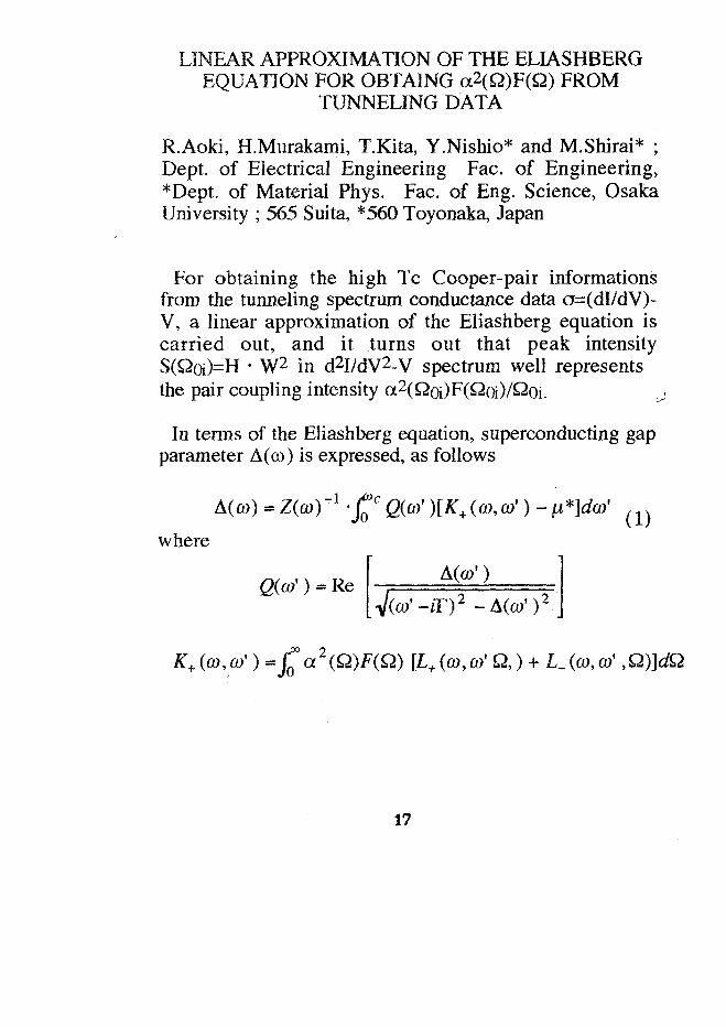
FEATURE OF THE ENERGY GAP IN YBa2Cu,O. FROM BREAK JUNCTIONMEASUREMENTS
T. Ekino, T. Minami, and H. FujiiFaculty of Integrated Arts and Sciences, Hiroshima University, Higashi-Hiroshima724, Japan
Superconducting energy gap in YBa,Cu3O7 have been investigated using breakjunctions. The tunneling conductance, di/dV, at T= 4.2 K shows no leakage aroundzero bias, while the gap edge peaks are broadened compared to the simple BCSdensity of states. These features suggest the spatial distribution of the energy gap orthe anisotropic j-wave pairing. The observed largest gap value, determined by thepeak-to-peak(p-/>) separation in dl/dV, is 140 meV, which corresponds to the 4A ofan SIS junction. The observed tunneling density of states is fairly well expressed bythe probability distribution of the energy gap using the BCS density of states.
Electron tunneling technique has been provided the most direct information aboutthe mechanism of superconductivity through the measurements of the quasiparticledensity of states[l]. However, the tunneling measurements using the high-rcsuperconductors have been confronted with serious difficulties because of the surfacedegradation of samples during the junction fabrication processes. One of the solutionsagainst the difficulties is to use the in situ break junction. Since this techniqueprovides the most clean and unaffected junction interface, intrinsic feature of thetunneling density of states can be obtained.
In this paper, we report on the tunneling measurements of the superconductingenergy gap in Y(Gd)Ba,Cu3O7 using the break junction technique. For themeasurements, polycrystaftine samples with Tc = 90 K and the resistive transitionwidth ATC < 1 K were used. The junctions were formed by fracturing the thinstrip-shaped sample in liquid helium just before the measurements. It is noted that inthe break junction method, the fractured surface will be rough so that the scatteringof tunneling electrons in the junction is expected to occur. In this case it is consideredthat the averaged tunneling density of states with respect to the Fermi surface isobtained. The tunneling conductance, dl/dV, were measured using a standard lock-intechnique with a constant modulation amplitude of 100 jiV.
Figure 1 shows the tunneling conductances from the different GuBa,Cu3O7(GBCO)break junctions at T=A3 - 4.7 K. In Fig. 1 (a), the magnitudes of the conductanceare largely different between opposite bias polarities, but the peak positions in dl/dVoccur at ± 70 mV. The gap structure is largely broadened compared to the simpleBCS denstity of states and the large leakage conductance is observed. On the otherhand, the gap-edge peaks in dl/dV in Fig. l(b) are much sharper than those in Fig.l(a), and no leakage conductance is observed around zero bias. The junction resistanceat the gap edge is 300 kfi in Fig. l(b), which is much higher than 400 Q. in Fig. l(a).Nevertheless, the peak-to-peak separation of 140 mV in dl/dV is similar with eachother and this is the largest value observed in our measurements. From these facts,the value of 140 meV is considered to be Ahpp of the SIS(S=Superconductor,I=Insulator) structure in the break junction, where the A is defined by the half
25

T)
GdBa2Cu307
(a)
0.2VOLTAGE (V)
»7 break junctions in (a) low and (b)Fig. 1 Tunneling conductances fromhigh junction resistance regimes.
value of the peak-to-peak separation in dl/dV of an SIN(N=Normal metal) junction.As- shown in Fig.l, the conductance peak position is almost independent of the shapeof the curve. This is different from the usual broadening of the BCS density ofstates, where the peak position is moved to higher bias with increasing the broadeningparameter[2]. The A_. = 35 meV is consistent with the largest gap value obtainedfrom the Andreev reflection measurements of YBCO[3] and is almost the same asthat of B i ^ C a C u P g single crystal[4]. The structure at the bias of + 50 mV in Fig.l(b) is probably due to ?Ap.Je from a lower r phase because the well defined gapstructure with 4/1^ = 100 meV was also reproducible in our measurements.
Figure 2 shows the tunneling conductance (solid points) from a YBCO breakjunction at T = 4.2 K with an s-wave like gap structure. This is our best data in asense that there is a wide zero-conductance bias region within the gap. The peaks indl/dV occur at ± 35 mV, while there is no leakage within ± 15 mV. Since thepeak-to-peak separation of 70 mV is half that of Fig.l, this can be attributed to the2A Je of an SIN junction which is accidentaly formed in the break junction. Thebackground conductance shown by the solid curve in Fig. 2 is obtained by the fittingusing the data between ± 6 5 - 8 5 mV. The curve is expressed by the parabolic shapeof a + p v + yVzwitha = 21.8 xl0'6[S],|3 = -3.3 x 10 "5 [S/V], and y = 3.3 x 10 "3
[S/V2][lj. The asymmetry of the background about zero bias is due to the asymmetricbarrier profile.
The normalized conductance, which is obtained from the raw data in Fig. 2devided by the background at each bias point, is shown by the open circles in Fig. 3.The asymmetric feature of the raw data in Fig. 2 is more or less diminished by thisprocedure, which makes the data more reliable. To evaluate the tunneling density ofstates for YBCO, we have fitted the experimental data in Fig. 3 with the calculated
26
so
40
(A=1 30
20
10
. ,00 -75 -50 -25 0 25 50Voltage (mV)
75 100
Fig. 2 Tunneling conductance from a YBa,Cu3O7 break junction. Solid points andsolid curve represent the experimental raw data and the fitted background (see text),respectively.
curve. For the fitting function, we here introduce the probability distribution of theBCS density of states as follows,
N.(E) = Nn(0) / (E2 - A2)l/2} g(A) dA (1)
where. N (E) is the superconducting density of states, Np(0) is the normal statedensity of states at zero bias, A is the energy gap, and g(A) is the weighting functionfor the probability distribution^]. We assume that g(A) = (2n) 8 exp[ -(A-A,,)7(28)] (the Gaussian distribution function) for A, < A < A2 and g(A) = 0 for A < A,, A} < A,where A,, and 8 are the average gap value and the standard deviation, respectively.The tunneling conductance were thus calculated and fitted to the experimental databy choosing appropriate values of Ao, 8, A,, and A^ as the fitting parameters. In thiscalculation, we put T= 0 K because thermal smearing at 4.2 K is not significant forthe superconductor with Tc = 90 K.
The fitting result is shown by the solid curve in Fig. 3. The calculated conductancecurve on the basis of the above assumption actually matches with the data especiallybelow the gap-peak biases. The disagreement between the experimental and calculatedcurves at higher biases is due to ambiguity of determining the background. Thefitting parameters are A,, = 31 meV, 8 = 6 meV, A, = 17 meV and \ = 61 meV forthe negative bias, and Ao = 33 meV, 8 = 10 meV, A, = 17 meV and A2 = 71 meV forthe positive bias, respectively. The significant feature of the fitting result is that it
27

.42
-100 -75 -25 0 25 50
Voltage (mV)75 100
Fig. 3 Conductance fitting result for YBajC^O, using the Gaussian distribution ofthe BCS density of states. Open circles and solid curve repesent the experimentaldata and the calculated curve using Eq. (l)(see text), respectively.
really needs a sharp cut off at A,, which indicates the existence of the minimum gapvalue in the quasiparticle excitation spectrum. The higher-energy cut off at A, =61-71 meV, which is larger than the SIN gap value of Ap.p = 35 meV, probablyreflects a mixture of the gaps from partly formed SIS junctions at the interface.
In conclusion, the measurements of the superconducting energy gap in YBajCu?O7using the break junctions showed the s- wave like gap structure. The obtained tunnelingconductance is fairly well fitted with the Gaussian distribution of the BCS density ofstates with the energy cut offs at both sides of the distribution. These featuresindicate the existence of either the real gap distribution due to the local distributionof oxygen concentration or the gap anisotropy in this compound.
This work was surported by a Grant-in-Aid for Scientific Research on PriorityAreas, "Science of High Tc Superconductivity" given by Ministry of Education,Science and Culture, Japan.
References[1] E.L. Wolf, Principles of Electron Tunneling Spectroscopy, (Oxford, New York,1985).[2] T. Ekino and J. Akimitsu, in Studies ofHigh-Tc superconductors, edited by A.V.Narliker (Nova, New York, 1992), Vol. 9, p. 259.[3] A.I. Akimenko, G. Goll, H.v. Lohneysen, and V.A. Gudimenko, Phys. Rev. B40,6409 (1992).[4] T. Ekino, T. Minami, H. Fujii, and J. Akimitsu, Physica C (to be published).

JOSEPHSON AND QUASIPARTICLE TUNNELING FORSUPERCONDUCTORS WITH PARTIAL DIELECTRIC GAPPING
A.M.Gabovich Crystal Physics Department, Institute of Physics of the NationalAcademy of Sciences, Kiev, Ukraine
UA9600435Josephson and quasiparticle current-voltage characteristics for junctionswith partially-gapped CDW- or SDW- superconductors are calculated. ExtraRiedel-like and Giaver-like peculiarities appear for voltages determined bythe superconducting gaps as well as the dielectric gap L.
The question whether the superconducting state and charge- (or spin-) densitywaves (CDW, SDW) really coexist has a long history and is still unresolved inexperiment directly. But many indirect data as well as theoretical considerationsspeak in favour of the promising coexistence possibility for various substances (see,e.g. [1-3]). In the temperature range where there are both the superconductingorder parameter A and the dielectric gap S (the latter accompanies CDW or SDW)various thermodynamic and transport properties should somehow differ from theBCS ones. Of course, the same should be valid for tunneling between CDW- orSDW- superconductors (both in symmetrical and in non-symmetrical junctions).Here we outline the main features of tunneling phenomena involving suchmaterials.
The consideration is based on the Bilbro-McMillan model [4] of the anisotropicmetal with nesting Fermi surface (FS) sections (1 and 2), where the gap £ developsbelow temperatures T = Td or 7^ (higher than the critical temperature Tc of thesuperconducting transition). Thus, the dielectrization is partial because the section3 of the FS is not influenced by the electron-hole pairing and may be affected onlyby formation of the gap A for T < Tc.
The superconducting order parameter will be considered hereafter to be spin-singlet and posessing s-wave symmetry and the dielectric order parameter to bespin-singlet (CDW) or spin-triplet (SDW). The corresponding energy gap 2 ischosen to be real (positive or negative). Imaginary order parameter 2 describesphenomena which have not yet been observed. The strong mixing of all branches ofthe non-reconstructed electron spectrum is suggested [4].
For CDW-superconductors the following normal and anomalous Green'sfunctions should be taken into account: Gnd, Ga, Fnd, and Fd. The "interband"function GA describes the influence of the electron-hole pairing on various metalproperties and is analogous to the Gorkov's functions Fnd (Fd) for the Cooperpairing. For SDW-superconductors the extra Green's function F& enters into the

problem. Clearly the explicit expressions for the functions involved are different forthe two cases [1].
The full current through the junctions with slowly varying bias voltages V(t) canbe expressed as follows:
(1)
Here e is the electron charge, I, is the Josephson current, I2 ts the interference pair-quasiparticle dissipative current, and J is the quasiparticle current. The componentsI,, I2, and J consist of several terms each. These terms correspond to variouscombinations of fs and G's. It is well known that there are singularities and jumpsin lj, 12, and J for definite V [5]. In our more complicated case the number of thefeature points is much larger.
As a result, for CDW-superconductors in the symmetrical case (CDW-metal/insulator/CDW-metal) we have jumps in the dependences I,(V) for D-A (forT = 0), where D = (A2+22)l/2 and the logarithmic singularities for eV - ID, A+D,arid 2A. Hereafter we assume eV > 0. Otherwise, one should take -eV = \eV\instead. For 12(V) and J(V) there are jumps for eV = 2D, A+D, and 2A andsingularities for D-A.
For the non-symmetrical junctions CD W-metal/insulator/ordinarysuperconductor, where the latter is characterized only by one superconducting gapd, the Riedel-rype logarithmic singularities for lt(V) will exist when eV = D+5,S±A, and jumps when eV = \D-d[ and |A-$ (for T * 0). The correspondingsingularities and jumps for I2 and J can be easily obtained from the Kramers-Kronig-like relations [5].
The SDW-superconductors are characterized by slightly more involvedquasiparticle spectrum in the parent undistorted phase. Thus, the results aredifferent from those for CDW-superconductors, although rather similar. In thesymmetrical case the Josephson current 1, has logarithmic singularities for eV =
2D± = |S±A| , H+ = D+ +D_, M±=D±+A and 2A and jumps for eV =
H_ = D+-D_ , N± = \D± - A| and T* 0. The same biases correspond to jumps
and singularities ofI2(V) andJ(V).
30

For non-symmetrical junctions the Riedel-type singularities should be observed
for eV = D±- S and A+S and jumps for eV = D±-5 and A-£, where 8 is.thesuperconducting gap of a conventional superconductor.
We want to stress that our results for I^(V) and Jm(V) in SDW-superconductors crucially depend on the sign of E. That is the direct consequence ofthe existence of C?a, and F^. These Green's functions are different for E > 0 and E <0 due to dissimilar structures of the elementary Fermi excitation spectrum in twocases [6].
The predicted peculiarities of the current-voltage characteristic behaviour can beobserved directly by tunnel or point-contact spectroscopies. Also, the Josephson
subharmonics for eV = eV9Se6al / ( 2 « + l ) , where n = 2,3,..., and Riedel
singularities in the microwave-irradiated junctions for eV + CO = ^V^eAeX, where cois the frequency, should appear.
To summarize, the dielectric gap not only changes the quasiparticle currentJ(V), that is quite natural, but can also drastically modify the Josephson coherentsuperconducting properties. One should bear in mind that the possible interestingcoherent effects [7] of sliding CDW or SDW are completely excluded fromconsideration here.
1. A.M.Gabovich, in: High-Tc Superconductivity, Experiment and Theory, edited byA.S.Davydov and V.M.Loktev (Springer, Berlin, 1992), p. 161.
2. E.Fawcett, H.L.Alberts, V.Yu.Galkin, D.R.Noakes, and J.V.Yakhmi, Rev. Mod.Phys. 66, 25 (1994).
3. K.Machida, Prog. Theor. Phys. Suppl. No 108, 229 (1992).4. G.Bilbro and W.L.McMillan, Phys. Rev. B 14, 1887 (1976).5. A.B.Zorin, I.O.Kulik, K.K.Likharev, and J.RSchrieffer, Fiz. Nizk. Temp. 5,
1139(1979).6. A.MIsmagilov and Yu. V.Kopaev, Zh. Eksper. Teor. Fiz. 96, 1492 (1989).7. A.L.Kasatkin, Fiz. Tverd. Tela25, 3091 (1983).
31
INELASTIC ELECTRON SCATTERING INFLUENCE ON THE STRONG-COUPLlNG OXIDE SUPERCONDUCTORS
A.M.Qabovich and A.I.Voitenko Crystal Physics Department, Institute ofPhysics of the National Academy of Sciences, Kiev, Ukraim
UA9600436The superconducting order parameter A and energy gap A are calculatedtaking into account the pair-breaking inelastic quasiparticle scattering bythermal Bose-excitations, e.g., phonons. The treatment is self-consistentbecause the scattering amplitude depends on A. The superconductingtransition for any strength of the inelastic scattering is the phase transition ofthe first kind and the dependences A(T) and AJT) tend to rectangular curvesthat agrees well with the experiment for high-Tc oxides. On the basis of thedeveloped theory the nuclear spin-lattice relaxation rate Rs in thesuperconducting state is calculated. The Hebel-Slichter peak in RS(T) isshown to disappear for strong enough inelastic scattering.
For high-T0 oxides one of the most important distinctions from the BCSbehaviour is the almost rectangular temperature, T, dependence of thosecharacteristics which are measured by resistive (tunnel and point-contact), infraredor Raman spectroscopies, and are generally identified with the superconductingorder parameter A or the energy gap A in the quasiparticle spectrum. The otherunusual feature of the these superconductors is the absence of the Hebel-Slichterpeak in the nuclear spin-lattice relaxation rate Rs below Te. This peak is a clearmanifestation of the s-wave Cooper pairing and traditionally serves as a check of itsrealization for various specific superconductors. We suggest that these phenomenaare due to the inelastic quasiparticle scattering in the superconducting state.
Here we develop a phenomenological approach, based on the BCS scheme,which treats the scattering processes as pair-breaking factors [1]. All theseprocesses are described by a single pair-breaking factor v= (TTC0)-\ where r is theinverse inelastic relaxation time, Tc0 is the critical temperature of the metal with noinelastic thermal scattering (v = 0), and h — kB = 1. We suggest that v depends onT as well as on the order parameter A of the superconductor. In turn, A is definedby the equation derived within the framework of Abrikosov-Gor'kov theory forsuperconductors with paramagnetic impurities [2]. This equation includes v as aparameter, so the problem becomes self-consistent.
We consider Cooper pairing to be of the s-type. We think that this assumptionagrees well with experiment (the situation is quite different from that for heavy-fermion substances). But there is another point of view suggesting a spin-singlet
32

anisotropic d-wave pairing. It is based, in particular, on experiments where the lowtemperature power dependences of transport properties were observed.Nevertheless, the s-wave character of the high-Tc oxide superconductivity issupported by gap-like Giaver one-particle tunnel currents for oxides, theconventional magnetic flux quantization in Nb-YBajCujOy rings, and usualtemperature and magnetic field dependences of the Josephson current inPb/insulator/Y,^P^BajCujO^g tunnel junctions.
We select the dependence v(t) in a rather general form v(t) = Atpf[t, S(t)],where t = T/Tc0, 6= A/Tc0, A and /? are the dimensionless parameters of the theory.The exponent J3 can be found both from theoretical considerations and fromresistive measurements, and usually falls into the interval 1 to 3.
The function f(t, 5) allows for the reverse effect of the electron spectrum gap onthe scattering process. In particular, it can be chosen as a constant, which makesthe problem non-self-consistent. But if the quasiparticle recombination processesmake the dominant contribution into inelastic scattering, it is reasonable to selectf(t, 5) in the form
f(t,S) = cxV[-S(t)/t]. (1)
This equation has been obtained [3] from Eliashberg equations not allowing forthe reduction of the real spectrum gap A (T) against the order parameter A(T):
(2)
where S^AJT^ is the dimensionless energy gap. So, we assume that the followingmodel will be more correct:
g() (3)
In Fig. 1 the temperature dependences of the superconducting order parameter8(1) are shown for various types of the pair-breaking factor. The dashed curve is theMiihlschlegel curve within a factor rc0/A(0) = y/it, where y = 1.7810... is the Eulerconstant. Curve 1 corresponds to our model with a temperature-dependent pair-breaking scattering but without self-consistency: v(t) = 0.5t. We remark that evenin this version of the theory the ratio 2A(0)/Tc0 is far in excess of its BCS value
33

Inly, the conclusion being in agreement with the majority of experimental data forHTSC. Curves 2 and 3 were calculated in the self-consistent framework of Eqs.(l)
and (3), respectively. Here A = 0.5 and /3= 1, the latter being common toYBa^UjO?. The calculations wereperformed only in the gap regiondefined by the condition v(t) S(l). Onecan see from Fig. 1 that the orderparameter becomes double-valued whentreating self-consistently. The dashedportions of curves 2 and 3 describe thelower branches connecting thebranching points and the points wherethe condition v(t) 8(t) fails. Oneshould note that curve 3 ends at theintersection point with curve 1 since v(l)- 5(t) here.
The double-valued character of A(T)
t = TIT.cOFig.l:
in Fig. 1 at the first-glance resembles one for the gap edge obtained in [4,5] withinthe Eliashberg theory. However, the calculations of these works led to the single-valued behaviour of the order parameter \(T) and the energy gap \CO, whichvanished continuously when 7" approached Te in line with the theory of second-order phase transitions. The double-valued nature of the order parameter A CO andhence the gap \(D survives, as our calculations show, for arbitrary small A and J3> 0, but the branching point rapidly shifts towards the close vicinity of 7'c when Abecomes small. Therefore, the predicted effect would not be observed for low-Tc
superconductors since it goes there beyond the accuracy of the experiment.The lower branches of curves 2 and 3 correspond to-unstable states which can
not be realized since the free energies of the superconducting state for them exceedthe free energies of the corresponding stable branches with larger order parameterACO- Therefore, the continuous behaviour of &(T) is interrupted at the branchingpoint and the phase transition of the first kind into the normal state occurs, so thatthe order parameter goes discontinuously to zero at T = 7C. The transition isdepicted by the vertical solid parts of curves 2 and 3. The transformation of thephase transition order in a similar situation, when the instability is driven by a non-equilibrium external electromagnetic radiation, was obtained in Ref.6.
The T-dependence of the nuclear spin-lattice relaxation rate in thesuperconducting state is the most popular among transport characteristics of high-Tc oxides. First of all, here the BCS theory leads to the non-monotonous behaviour
34
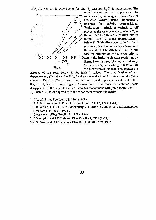
of RS(T), whereas in experiments for high-Tc ceramics RS(T) is monotonous. Theother reason is its importance forunderstanding of magnetic properties ofCu-based oxides, being magneticallyunstable for definite compositions.Without any intrinsic or extrinsic cut-offprocesses the ratio p = RJRn, where Rn isthe nuclear spin-lattice relaxation rate innormal state, diverges logarithmicallybelow Tt. With allowance made for theseprocesses, the divergence transforms intothe so-called Hebel-Slichter peak. In ourcase the elimination of the singularity is
1 .Odue to the inelastic electron scattering bythermal excitations. The main challengefor any theory describing relaxation in
& the superconducting state is to explain theabsence of the peak below Tc for high-Tc oxides. The modification of thedependences p(0), where 0= T/Tt, for the most realistic self-consistent model (3) isshown in Fig. 2 for /? = 1. Here curves 1-5 correspond to parameter values A = 0.1,0.2, 0.5, 1, and 1.5. From Fig.2 it follows that in this model the coherent peakdisappears and the dependence p(T) becomes monotonous with jump to unity at T =Tc. Such a behaviour agrees with the experiment for ceramic oxides.
1. J.Appel, Phys. Rev. Lett. 21, 1164 (1968).2. A.A.AbrikosovandL.P.Gor'kov, Sov.Phys.JETP 12, 1243 (1961).3. S.B.Kaplan, C.C.Chi, D.N.Langenberg, J.J.Chang, S.Jafarey, andD.J.Scalapino,
Phys.Rev.B 14, 4854 (1976).4. C.R.Leavens, Phys.Rev.B 29, 5178 (1984).5. F.Marsiglio and J.P.Carbotte, Phys.Rev.B 43, 5355 (1991).6. C.S.Owen and D.J.Scalapino, Phys.Rev.Lett. 28, 1559 (1972).
35

JOSEPHSON CURRENT IN SUPERCONDUCTINGSUPERSTRUCTURE.
G.A.Gogadze. UA9600437B.I.Verkin's Institute for Low Temperature Physics & Engineering by theAcademy of Sciences of Ukraine, Lenin av.47, Kharkov 310164, Ukraine.
The Josephson current in superconducting superlattices is investigated.
1. The Josephson-type model structure which consists of the periodicallyalternating superconducting (S) and ̂ normal ,(N) metallic layers(superconducting superlattice) was considered. The period of this structureequals d = ds + dh (there ds , dh are the thicknesses of S- and N-layers,consequently). The period is large to be compared with the atomic scale but itis comparable with the superconductor coherence length £ (T). TheJosephson current in the superlattice depends on both the Fourier-transformof the thermodynamical Green function of superconducting superstructureand the Green function of normal metal. The Josephson current near thecritical temperature Tc is a complex function of the phase difference <pbetween the nearest superconducting layers. If we introduce the dimensionlessparameters a = JtTd/V y =d s /dh and believe that parameter 1 / [a(l+y)]is small then we can obtain the current as a series (there V is the Fermi-velocity) :
i(!P ) = ^f- • | f [[ A (a) - B (a; y) ] sin* +
" (1)
00
y e-2a(2n+l) 4 V"< e-2a(2+y)(2n+l)where A (a) = JL* 5-, B (a; y) = -TT— JLA
n=0 \ nn=0
The critical current of the superconducting superstructure is
36

J(*}" ̂ r • £ [ A"B
In the limit case y -* oo the expression obtained is equal to the criticalcurrent of the S-N-S contact.
2. The essential role can be played by the modification of the superlatticecondensate spectrum from the continuous to bandy one while studying thethermodynamical and kinetic characteristics of the superconductingsuperlattices (SS). In paper [1] the possibility of existence of the bandcondensate spectrum in SS was pointed out for the first time. It waspredicted.that the condensate spectrum slipping became available startingfrom a critical level of modulation of the order parameter SS. The condensatestates in different bands are distinguished with the modulus of order parameterin space. The Josephson specific of the SS behavior appears in the possibilityof upper in energy current bands of condensate in excited bands with theordinary superconductive current, which corresponds to the lowest band.Thepresence of the SS energy bands makes it possible for the condensatetransitions from one quantum state to another as an macroscopic system.
Let us study the band states stability of SS. The consideration is done inframework of the Ginzburg-Landau (GL) scheme on a superconductive filmthe order parameter of which is depressed due to proximity effect by peri-odically deposited normal metal layers.
The Ginzburg-Landau equation in normalized variables for SS is:
+ 00
d V ^ + V(x) [ 1- | V(x) 12 ] = X 2 d (x- m d) V(x) (3)d x m=-oo
where V (x) is the order parameter of SS, d is the period of superlattice, thedimensionless constant A > 0 characterizes the degree of suppression ofsuperconductivity in the points x = md. The Kronig-Penney model for SSwith delta functions is true, when the effect of the pair-breakingmechanism is localized on distances much smaller than d,£ (T). The states of
51
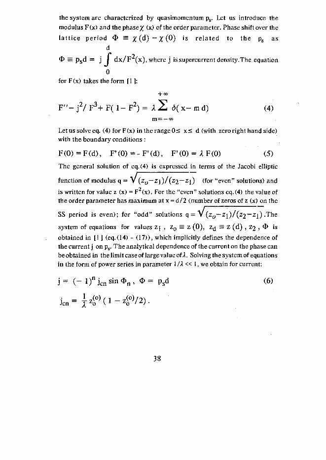
the system are characterized by quasimomentum ps. Let us introduce themodulus F(x) and the phased (x) of the order parameter. Phase shift over thelattice period <I> = % (d) - % (0) is related to the ps as
d
4> = p sd = j I d x / F (x), where j is supercurrent density.The equation
0for F(x) takes the form [1 ]:
+ 00
F"- j 2 /F 3 +F( l -F 2 )= A 2 <5(x-md) (4)m= —oo
Let us solve eq. (4) for F(x) in the range 0< x< d (with zero right hand side)with the boundary conditions :
F(O)=F(d), F(0)=-F'(d), F'(O) = AF(O) (5)
The general solution of eq.(4) is expressed in terms of the Jacobi elliptic
function of modulus q = V (zo—Z])/(z2—z{) (for "even" solutions) and
is written for value z (x) = F2(x). For the "even" solutions eq.(4) the value ofthe order parameter has maximum at x = d/2 (number of zeros of z (x) on the
SS period is even); for "odd" solutions q = V(zo—z\)/{z2—z\) .The
system of equations for values Z\ , z0 = z (0), Z(j = z (d) , zj > *& *s
obtained in [1 ] (eq.(14) - (17)), which implicitly defines the dependence ofthe current j on ps. The analytical dependence of the current on the phase canbe obtained in the limit case of large value of A. Solving the system of equationsin the form of power series in parameter 1IX « 1, we obtain for current:
j = ( - l ) n j c n s i n O n , 0»= psd (6)
,- - I 7(°) ( 1 _ 7(°)/2)Jen ~ X zo V l zo ' z) •
38

( ) (7)
where K(q) is the complete elliptic integral of the first kind.
It is necessary to consider the sign of the second variation of thethermodynamical SS potential W for the investigations of the thermodynamicalstability of the solutions of GL equations. Let us consider SS in the form ofclosed ring with one weak link, when the phase F is fixed. It can be shown,that F(x) is stable, when the lowest level of the operator 3F2(x) - 3 j 2 / F4(x)-
ry ry
- 1— d /dx is positive. The equation for the eigen functions and eigenvalues of this operator in the current absence can be transformed to the Lameequation of degree 2 :
= {6q2sn2(a;q)-A}u(a) ; (8)da
u (0) =u [2 (n+l)K(q) ] = 0, n = 0,l,2,...
where A = ( 1 + q 2 ) (1+e) = 2(1+ £) / ( 2 - zQ0)) .The values z^0) are
quantized by the condition (7). It follows from the connection between X and
e that £ on) = X (")/( 1 - q2) - 1 > 0, i.e. stability band condition is of
the form:
A on ) > 1 + q 2 (9)
We choose the functions Uj(a) and U2 (cc) (depending from the elliptic
0 ' (cc\
functions H( a ± a j) § (a) and Z(a) = Q ; . ' , which satisfy to the bound-
ary condition (8) as linear independent solutions of the Lame equation.The
fulfilled analysis showed that the smallest eigen value has the solution in the
form sn a dn a. The condition XQ = 1+ 4q 2 > 1 + q2 is fulfilled.i.e. the
band is stable.
1. OmeVyanchuk A.N.,Gogadze G.A.,Kulik I.O..Sov.J.Low Temp.Phys. 6(1),19 (1980).

NONEQUILIBRIUM STATES OF HIGH Tc YBCOSUPERCONDUCTORS UNDER TUNNEL INJECTION OFQUASIPARTICLES
I. Iguchi, Q. Wang, K. Lee and K. Yoshida UA9600438
Institute of Materials Science, University of Tsukuba, Tsukuba, Ibaraki, 305 Japan
The nonequilibrium states of high Tc superconductors are investigated by means of tunnel
injection of quasiparticles using Pb(or Au)/MgO/YBCO tunnel junctions. The effective
critical-current reduction due to tunnel injection is observed, whose behavior is different
from simple heating. The observed results suggest that the resultant nonequilibrium
states may also differ from those described by conventional nonequilibrium models.
The nonequilibrium states of low 7c metal superconductors under highquasiparticle injection attracted considerable attention. They can be created byinjecting photons or quasiparticles into a superconducting film. Under stronginjection of quasiparticles, various interesting phenomena such as the gapreduction, the spatial instability, the multiple gap states have been observed
[1-5] . On the other hand, there have been very few reports on thenonequilibrium states of high Tc superconductors. By means of opticalexcitation .technique, both bolometric and nonbolometric reponses to pulsedlaser excitations have been observed [6-8] . For tunnel injection ofquasiparticles, we have recently reported the strong critical-currentsuppression under tunnel injection current [9,10] . Here we report theseobserved results on tunnel injection of quasiparticles into a superconductingYBCO film and the further extended works.
The samples were prepared by fabricating a runnel junction onto a YBCOstripline by in situ deposition technique. First, a YBCO film was epitaxiallygrown onto a MgO(lOO) single crystal. The film was patterned out either byin situ metal mask technique or by photolithography technique. The filmwidth was 0.2mm for the former case and 15-60 fi m for the latter case. Thefilm thickness was 40-100nm. The junction was formed by depositing MgObarrier of l-4nm thick and subsequently a Pb or an Au counterelectrode.
The measurements for Pb(or Au)/MgO/YBCO junctions were performed by
40

feeding two currents in a YBCO film, one across the junction( injector
current: Bnj), the other through a YBCO film only (transport current I). The
Pb/MgO/YBCO injector junctions showed a reasonable gaplike structure at
V= A/e~20mV and a sharp Pb gap structure [11,12] .
It was found that the film critical current Ic decreased as Iinj was increased.
Figure 1 shows an example for the I-V characteristics under different injector
current Iinj for an Au/MgO/YBCO junction. The junction resistance was
about 30 Q. The positive current axis corresponds to the case that / flows in
the same direction as Iinj in a YBCO film. Ic (=20mA) was suppressed to
zero at Iinj=14mA, suggesting the effective gap reduction due to quasiparticle
injection. The second bend in the I-V curve may correspond to the critical
current in the unperturbed film part. The current gain defined by
Ic(Iinj=0)/Iinj(Ic=0) was about 1.45. Figure 2 depicts the plot of Ic as a
function of Iinj at 4.2K for the other sample. The solid line corresponds to the
case that only the current summation effect is involved. The calculation for
simple heating model (dashed line) yielded the curve with downward
Fig.l Current-voltage characteristics of a YBCO Fig.2 YBCO film critical current Ictilm
under different injection current Iinj as a function of injection current Iiaj
41
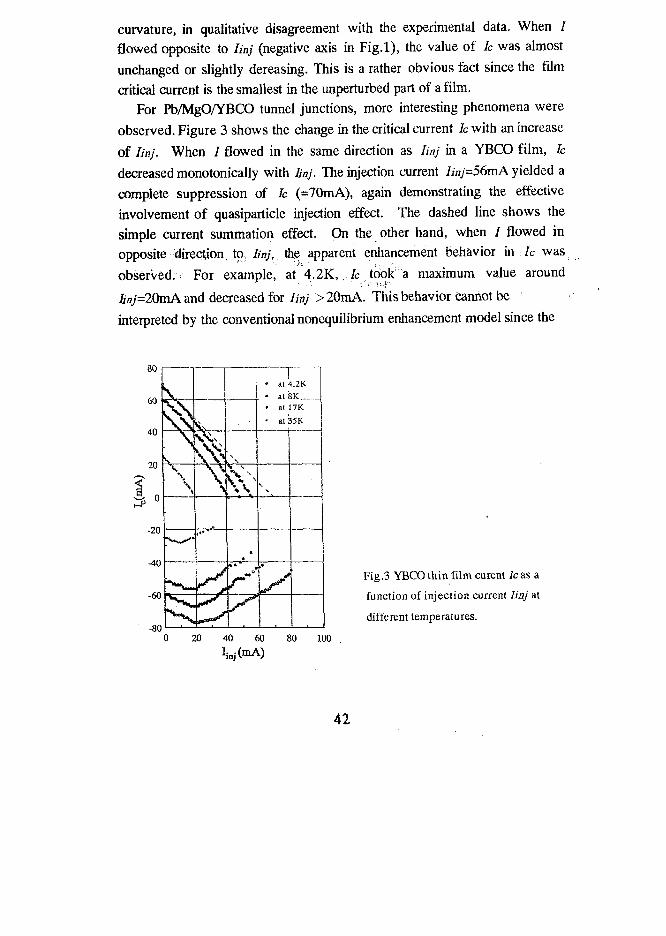
curvature, in qualitative disagreement with the experimental data. When /flowed opposite to Iinj (negative axis in Fig.l), the value of h was almostunchanged or slightly dereasing. This is a rather obvious fact since the filmcritical current is the smallest in the unperturbed part of a film.
For Pb/MgO/YBCO tunnel junctions, more interesting phenomena were
observed. Figure 3 shows the change in the critical current Ic with an increase
of Unj. When / flowed in the same direction as Iinj in a YBCO film, k
decreased monotonically with Iinj. The injection current Iinj=56mA yielded a
complete suppression of Ic (=70mA), again demonstrating the effective
involvement of quasiparticle injection effect. The dashed line shows the
simple current summation effect. On the other hand, when / flowed in
opposite direction, to Iinj,, the apparent enhancement behavior in Ic was
observed. For example, at 4.2K,./c tooka maximum value around
2rn/=2QmAand decreased for Iinj >20mA. This behavior cannot be
interpreted by the conventional nonequilibrium enhancement model since the
80
60
40
20
-20
-40
-60
\V\ \
r• al 4.2K• al8K• al 17K• al 35K
-80' l-0 20 40 60 80 100
Fig.3 YBCO thin film curent /cas a
function of injection current Iiaj at
different temperatures.
42

bias voltage for the injector junction is much greater than A • The
enhancement of Ic in the experimental situation may be interpreted by
assuming that Ic of a YBCO film underneath a junction part is smaller than
that outside a junction part due to possible damage by multilayer deposition
process. It should be emphasized that the enhancement can be observable only
for a certain range of junction resistance (75 Q — 300 Q) The mechanism of
enhancement of Ic is, however, still unclear. We conjecture that it may arise
from either the inelastic scattering effect (hence creating preferable
nonequilibrium enhancement condition) due to injection of very high energy
quasiparticles (~0.5eV) or the local current distribution in a junction part.In conclusion, the tunnel injection of quasiparticles into a YBCO film
yielded a variety of interesting phenomena, which may be different from thoseobserved for low Tc superconductors. Further study is necessary to clarifythe nonequilibrium states of high Tc superconductors.
1. D. N. Langenberg, in Proceedings of the 14th International Conference on Low
Temperature Physics, edited by M. Krusius and M. Vuorio (North-Holland, Amsterdam,
1975) Vol. V,p.223.
2. A.-M. S. Trembley, in Nonequilibrium Superconductivity, Phonons and Kapitza
Boundaries, edited by K. Gray (Plenum, New York, 1981), p.309.
3. I. Iguchi, Phys. Rev. B16, 1954 (1977).
4. G. A. Sai-Halasz, C. C. Chi, A. Denenstein and D. N. Langenberg, Phys. Rev. Lett.
33,215(1974).
5. I. Iguchi and D. N. Langenberg, Phys. Rev. Lett. 44, 486 (1980).
6. S. G. Han, Z. V. Vardeny, K. S. Wong and O. G. Symko, Phys. Rev. Lett. 65, 2708
(1990).
7. A. Frenkel et al., Appl. Phys. Lett. 54, 1594 (1989).
8. M. Johnson, Appl. Phys. Lett. 59, 1371 (1991).
9. I. Iguchi, K. Nukui and K. Lee, Phys. Rev. B50, 457 (1994).
10. Q. Wang and I. Iguchi, Physica C228, 393 (1994).
11. I. Iguchi et al . ,Jpn.J . Appl. Phys. 29, L614 (1990).
12. I. Iguchi and Z. Wen, EEETrans. Mag. MAG-27, 3102 (1991).
43
BARRIER PROPERTIES OF HTSC TUNNELJUNCTIONS
A.I.Khachaturov, M.A.Belogolovskii UA9600439A.Galkin Donetsk Physico-Technical Institute of Ukrainian NationalAcademy of Sceinces, Donetsk 340114, Ukraine
It was found that the overall shape of the normal state tunnel conductance ofmetal oxides with low Fermi energies is very sensitive to the barrier height andthickness. It was shown that this curve can differ considerably from the usualtunnel characteristics known from the tunnel spectroscopy of conventionalmetals.
In the most part of metal oxide tunneling investigations in analyzing normalstate anomalies of their tunnel conductance it is assumed that its ideal behaviordoes not differ from that of the conventional metals, i.e. for low voltages itshould be a constant and should increase as a parabola for high voltages(« 1 eV). In any case [ 1 ] it was universally accepted that this curve increasesmonotonically and therefore any deviation from this behavior should beregarded as a peculiarity. But such an approach does not take into account thatthe metal oxide differs considerably from conventional metals not only in theirsuperconductive properties but in a number of normal ones, hence goodreasons exist for revising some of the fundamentals accepted in the tunnelspectroscopy of conventional metals.
The aim of the present work is to answer for the question "What differences inoverall shape of a (V) could be caused by the small value of the Fermi energyin metal oxides, that is very much less than in the conventional metals ?". Inour calculating we take care not to deviate remarkably from the initialsuggestions on the nature of the potential barrier made by previousinvestigators [1,2] and used the simple model proposed Brinkman et al intheir classic work [ 1 ]. Following these authors we chose the trapezoidal barrierto present insulator <p (z,V) == (pi+ (z /d) (<P2~eV~<Pl)> where^pj and<P2 are the barrier height on opposite sides of the tunnel junctions with zeroapplied voltage, d is the barrier thickness. As far as we interested in
44

conductance variations over a large bias range a zero-temperature evaluationwill suffice for the present work.
In this paper we restrict attention to symmetrical tunnel junctions with thesame Fermi energies in both electrodes Ep =» EF « EF . This conditions is
fulfilled automatically in the break-junctions. In other types of contacts itexists if both electrodes are fabricated from the same materials. As pointedout in [3 ] symmetrical tunnel junctions can be also formed by asymmetricalelectrodes for example in the point contacts between the metallic tip andceramic. In this case the former intimately contacts with one of conductivegrains of the ceramic and electron tunneling takes place betweenneighboring grains in a bulk of ceramic.
The calculations of the tunnel conductance a (V) were performed using theexpression for tunneling current proposed in [2 ]. **
J(V) =H
0
P(EZ,V) dE
J(EFi-Ez)P(Ez,V)dEz (1)
One of the conclusions by Brinkman et al [1 ] is that the shape of the curve a(V) does not depend on the Fermi energy EF. Our calculations for the
rectangular barrier with the fixed values of the thickness of d - 10 A and the
height of (p = <p i= <P2 = 3eV show that this is true only for the relatively large
Fermi energies. Indeed, curve 3 and curve 4 in Fig. 1 obtained for EF - 3 eV and
EF = lOeV respectively practically coincide. But at low EF less than 1 eV
the delineation of a (V) changes drastically. At EF = l.OeV (curve 2, Fig.l) a
zero bias "resisting peak" anomaly is seen in this curve and at EF=0.5 eV the
tunnel conductance decreases throughout the entire range of voltages.
45

1.05
0.91
-100 0 100
V,mV•if
Fig.l
The barrier thickness d proved to have a pronounced effect on the overallshape of the tunnel conductance. As shown in Fig.2 (curve 4 and curve 5) atquite large thicknesses d - 15-20A the conductance versus voltage appearsroughly as a parabola but when thickness decreases down to 10 A (curve 2,Fig.2) and 5 A the behavior of the o (V) undergoes the profound alternations.Taking into account that in many types of junctions (for example pointcontacts) the barrier thickness can be changed quiet easily (often by anuncontrol fashion) the reason of conflicting results in the tunneling literaturebecome understood.
The set of plots in Fig.3 shows the pronounced effect of changing the barrierheight on the shape of the a (V) at low EF. The fixed parameters here are
Ep = 0.5eV and d =10A. Curve 1 are calculated for <p = 3 eV, curve 2 for <p =
1 eV, curve 3 for <p = 0.5 eV, curve4 for 0.3 eV. As we see the usual parabolicshape has only curve 1 whose barrier height less than Fermi energy EF .
Let us discuss some simple reasons that on our opinion are good enough forthe qualitative understanding of the nature of the effects under consideration.It is instructive to recall that the band density of states of three dimensionalmetal with the spherical Fermi ocean decreases rnonotonically by a square
46

1.10
0(0)
0.90-100
Fig.3 Fig.4
root law N(E)/N(0) = ( 1 - E / E F ) 1 / 2 when moving to the bottom of theconductance band. In the case of conventional metal tunneling spectroscopythis factor can be ignored because of at low voltages the density of state canbe regarded as a constant and at large voltages, when the decreasing in N(E)becomes remarkable, the behavior of the tunnel conductance is dominated bythe exponentially increasing tunneling probability P (Ez ,V). For metal oxidecompounds with a small Fermi energy we have another situation. In this casethe density of states considerably decreases already in the voltage region nearzero bias where the tunneling probability can be considered not to depend onboth the energy Ez and applied voltage V. Then from formula (1) we reach theconclusion that the density of states N(E) = a(V) /a(0) = 1 - eV/EFlinearly decreases, i.e. it behaves in the same fashion as the curve 4 inFig.4.
The inclusion of the preexponential term does not qualitativelyalter our results. This point is illustrated in Fig.4 where thecalculations for the same barrier parameters as in Fig.3 arerepeated taking this term into account. For this we used theexpression given in [ 1 ] that was obtained in the sharp boundarylimit.Conclusions. In contrast to the tunneling spectroscopy of conventional metals
47

the overall shape of the conductance versus voltage dependence of metal oxidetunnel junctions proved to be sensible to barrier parameters <p and d. Theirmagnitude can be determined by many factors (including little controlled)and, therefore, can alter their values considerably even for one experimentalcycle. In our point, namely this reason should be regarded as the main sourcea great deal variation in HTSC tunneling spectra seen from differentexperiments. The work is supported in part by the State Committee of Scienceand Technology of Ukraine.
Acknowledgements. The authors are very grateful to the Japan Society forPromotion of Science for supporting the Symposium where this work ispresented. We are also indebted to V.M.Svistunov for his encouragementduring the investigation.
1. W.F.Brinkman , R.C.Dynes, J.M.Rowell Journ. of Appl.Phys. 41 (1970)1915.
2. R.B.Floyd, D.G. Walmsley J.Phys.C: Solid state Phys., 11 (1978) 4601.3. V.M.Svistunov, AJ.Khachaturov, M.A.BelogolovskiiModern.Phys.Let.B., 4
(1990) 111.
48

UA9600440

QUANTUM- AND SUBQUANTUM CONDUCTANCE IN SB CONTACTS
J. M. Krans", I. K. Yanson* and J. M. van Ruitenbeek"
aKamerlingh Onnes Lab., P.O. Box 9506, 2300 RA Leiden, The Netherlands6Verkin Inst. for Low Temp. Physics and Engineering, 47 ,Lenin Av. ,310164Kharkov, Ukraine
Using a mechanically controllable break junction atom-sized Sbcpntactsare studied at liquid helium temperature. The absence of conductancequantization, which, if present, would be clearly distinguishable from ,. v
conductance steps resulting from atomic rearrangements, is rfjscussed. f
Mechanically controllable breakjunction (MCB) technique, scanning tunnel-;
ing- and atomic force microscopy (STM and AFM) have, been used extensivelyin recent years to study the conductance in atom-sized metallic pointcontactswith variable constriction diameter [1-5]. An important item in experimentson these systems is the possible existence of conductance quantization. Thep-,,.retically, continuous variation of a mesoscopic constriction diameter (which isof the order of the Fermi wavelength, Ap) leads to discrete steps in the con-ductance ofexactly the quantum unit, 2e2//i, in case of ballistic current flow.This quantum size effect, described by the Landauer formula [6], is due toquantization of the transverse electron motion in the constriction. Experimen-tally, in metallic contacts discrete steps in the conductance are observed as thecontact size is changed by varying the pressure of the contact. These steps areof order 2e2//i, but not exactly reproducible at integer values of this quantumunit. The diameter of the metallic contact, in which the Fermi wavelength iscomparable to the atomic radius, can not be varied continuously due to the fi-nite size of the atoms. The non-reproducible conductance steps are attributedto strain-induced atomic rearrangements in the contact, such as those found inmolecular dynamics simulations [7].
In the present experiment atom-sized contacts are studied for the semi-metal Sb using an MCB at liquid helium temperature. In a semimetal thenumber of carriers per unit volume is small compared to typical metals: inSb n«5-1019cm~3 in each band (for Cu n«91022cm~3). In a free electrongas approximation this results in AF«55 A (for Cu AF«4.5 A). Because of thislarge Fermi wavelength it should be possible to make a clear distinction bet-ween steps resulting from the above mentioned quantum size effect and thoseresulting from geometrical rearrangements.
49
The samples of the very brittle single crystals of Sb are spark-cut to theshape of a thin bar with approximate dimensions 0.5x0.5xl5mm. Into thecenter of the bar, which is glued on a phosphor bronze substrate, a notchto about halfway the diameter was spark-cut. By bending the substrate thesample was broken at the notch at 4.2 K, under UHV conditions. The size ofthe extremely stable contact can be adjusted on an atomic level over a widerange down to one atom by applying a voltage over a piezo element, by whichthe bending of the substrate is controlled. This voltage Vp is proportional tothe displacement of the electrodes. From the sample geometry we estimatethat IV corresponds to ~0.05-0.lA. The temperature for the measurementspresented was between 1.3 and 4.2 K.
tt
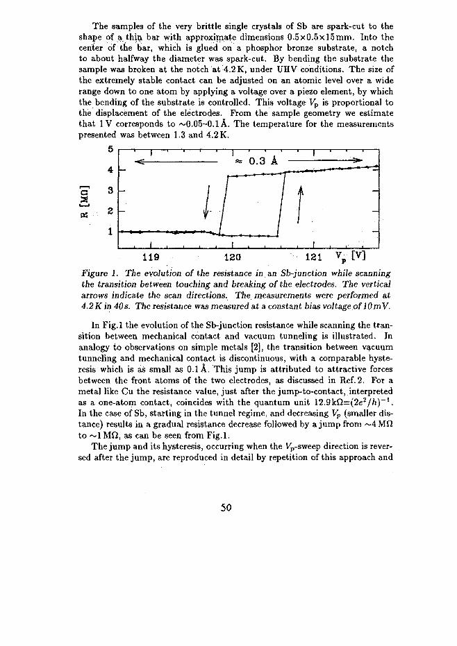
119Figure 1. The evolution of the resistance in an Sb-junction while scanningthe transition between touching and breaking of the electrodes. The verticalarrows indicate the scan directions. The measurements were performed at4.2K in 40s. The resistance was measured at a constant bias voltage of 10mV.
In Fig. 1 the evolution of the Sb-junction resistance while scanning the tran-sition between mechanical contact and vacuum tunneling is illustrated. Inanalogy to observations on simple metals [2], the transition between vacuumtunneling and mechanical contact is discontinuous, with a comparable hyste-resis which is as small as 0.1 A. This jump is attributed to attractive forcesbetween the front atoms of the two electrodes, as discussed in Ref. 2. For ametal like Cu the resistance value, just after the jump-to-contact, interpretedas a one-atom contact, coincides with the quantum unit 12.9kQ=(2e2/ft)~1.In the case of Sb, starting in the tunnel regime, and decreasing Vp (smaller dis-tance) results in a gradual resistance decrease followed by a jump from ~4 MQto ~1 Mfi, as can be seen from Fig.l.
The jump and its hysteresis, occurring when the V -̂sweep direction is rever-sed after the jump, are reproduced in detail by repetition of this approach and
50
retreat sweep over a small Vp-range. For R > 4 MQ in Fig. 1 decreasing or in-creasing Vp over a larger range gives perfectly reproducible smooth resistancebehavior, which is characteristic for the vacuum tunneling regime. At largeelectrode separation the resistance depends exponentially on the distance. Thelogarithmic slope is in good agreement with the literature value of the work-function of Sb. For R < 1 Mfi larger V̂ >-sweeps do not reproduce: the contactarea between the two Sb-surfaces can not be controlled reversibly.
For a series of measurements on different Sb-samples the resistance valuejust after the jump-to-contact ranges mostly between (approximately) 1 and2 Mfl, although values 50 % larger and smaller are sometimes found. This highresistance value can be explained by the large Ap of the electrons in a semimetalcompared to a simple metal. Atom-sized contacts of Sb have a transverse lineardimension much smaller than Xf. This implies that in these contacts there areno ballistic conducting states at Er, so that only tunneling contributes to thecurrent, resulting in a conductance much smaller than 2e2/ft.
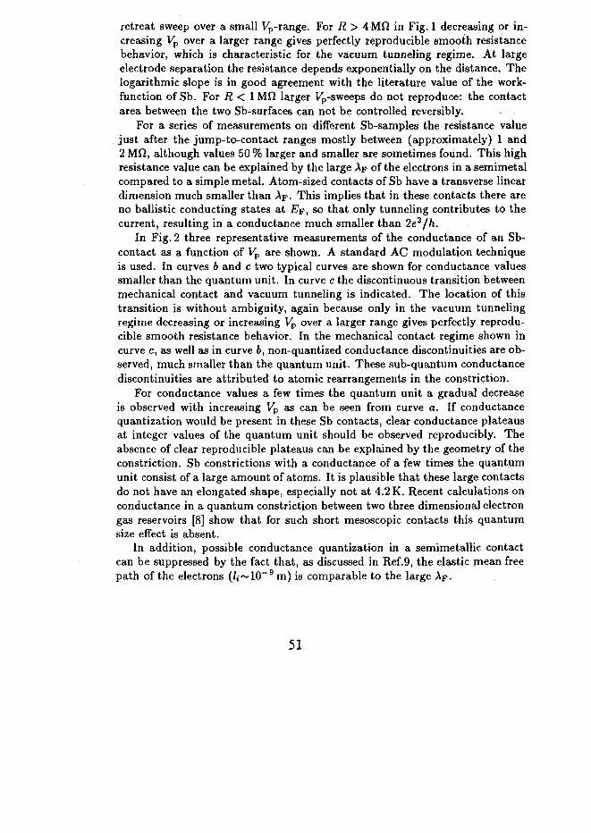
In Fig. 2 three representative measurements of the conductance of an Sb-contact as a function of Vp are shown. A standard AC modulation techniqueis used. In curves b and c two typical curves are shown for conductance valuessmaller than the quantum unit. In curve c the discontinuous transition betweenmechanical contact and vacuum tunneling is indicated. The location of thistransition is without ambiguity, again because only in the vacuum tunnelingregime decreasing or increasing Vp over a larger range gives perfectly reprodu-cible smooth resistance behavior. In the mechanical contact regime shown incurve c, as well as in curve fc, non-quantized conductance discontinuities are ob-served, much smaller than the quantum unit. These sub-quantum conductancediscontinuities are attributed to atomic rearrangements in the constriction.
For conductance values a few times the quantum unit a gradual decreaseis observed with increasing Vp as can be seen from curve a. If conductancequantization would be present in these Sb contacts, clear conductance plateausat integer values of the quantum unit should be observed reproducibly. Theabsence of clear reproducible plateaus can be explained by the geometry of theconstriction. Sb constrictions with a conductance of a few times the quantumunit consist of a large amount of atoms. It is plausible that these large contactsdo not have an elongated shape, especially not at 4.2 K. Recent calculations onconductance in a quantum constriction between two three dimensional electrongas reservoirs [8] show that for such short mesoscopic contacts this quantumsize effect is absent.
In addition, possible conductance quantization in a semimetallic contactcan be suppressed by the fact that, as discussed in Ref.9, the elastic mean freepath of the electrons (/,~10~9m) is comparable to the large Ap.
51

100 150 [V] , 200
4r-, 3
< 2
'» 1
i~J 1.0
o
o
0.5 -
0.0 L
_ 1
1
- \
-
-
1
11
1
• 1 .
1 - ,
11
1
1
\
1
1 1 1 , 1— «=12 A
1 1 1 11 1
«=2 A
mechanicalcontact
'i
1 I I
1 1 11
I
vacuumtunneling
I _
1 -
( b ) -
(c)"§ 0.06° 0.04
0.020.00
Figure 2. Three examples of the conductance of an Sb-contact at 1.3Kas a function ofVp, with Vp increasing. The curves are recorded for threedifferent Vp-sweeps, in ~30s using a current modulation of a few nA. Inall three plots every tick on the horizontal axis corresponds to Vp=10V.
[1] C.J. Muller, J.M. van Ruitenbeek, and L.J. de Jongh, Phys. Rev. Lett.69, 140 (1992) and references therein.
[2] J.M. Krans, C.J. Muller, I.K. Yanson, Th.C.M. Govaert, R. Hesper andJ.M. van Ruitenbeek, Phys. Rev. B 48, 14721 (1993).
[3] N. Agrait, J.G. Rodrigo and S. Vieira, Phys. Rev. B 47, 12345 (1993).[4] J. M. Krans, C.J. Muller, N. van der Post, F. R. Postma, A. P. Sutton, T. N.
Todorov and J.M. van Ruitenbeek, Phys. Rev. Lett., to appear.[5] J.I. Pascual, J. Mendez, J. Gomez-Herrero, A.M. Baro, N. Garcia and Vu
Thien Binh, Phys. Rev. Lett. 71, 1852 (1993); L. Olesen, E. Lasgsgaard,I. Stensgaard, F. Besenbacher, J. Schi0tz, P. Stoltze, K.W. Jacobsen andJ.K. N0rskov, Phys. Rev. Lett. 72, 2251 (1994).
[6] R. Landauer, IBM J. Res. Dey. i , 223 (1957).[7] T.N. Todorov and A.P. Sutton, Phys. Rev. Lett. 70, 2138 (1993).[8] J.A. Torres, J.I Pascual and J.J. Saenz, Phys. Rev. B 49, 16581 (1994).[9] I.K. Yanson, N.N.Gribovand O.I. Shklyarevskii,JETPLett.42,195 (1985).
52

UA9600441

COMMON FEATURES IN JOSEPHSON SELF-RADIATION ANDSHAPIRO STEPS FOR VARIOUS HTSC JUNCTIONS
Kiejin Lee and Ienari IguehiInstitute of Materials Science, University of Tsukuba, Tsukuba, Ibaraki3Q5, Japan.
Abstract—We have investigated the Josephson self-radiation from different typesof YBCO thin film junctions: natural grain boundary junctions, step-edge junctionsand bicrystal junctions. The self-radiationpowers were directly detected using atotal power radiometer receiver system with receiving frequencies off =11-72 GHz.For all types of junctions the observed self-radiation linewidths were deviated fromthe theoreticalRSJ values due to noise source in the junction boundaries. Formicrowave-induced Shapiro steps, the harmonic steps and additional subharmonicsteps with their quasi-periodic variation satisfying the Josephson equation, V=(n/m)(hf/2e), were clearly observed. The results on the observed ac and dcJosephson effects will be discussed in terms of a model which treats the grainboundary junction as a multi-connected Josephson junction having a non-sinusoidalcurrent-phase relation.
Recently, many types of HTSC Josephson junctions, such as natural grainboundary junctions]!], step-edge junctions[2] and bicrystal junctionsf3] have beeninvestigated for the purpose of microwave device applications. For natural grainboundary junction, the junction properties are strongly influenced by themicrostructure of grains, which behave in many ways like a random arrangement ofweak links, sometimes called a Josephson medium. For step-edge junctions, a c-axis oriented YBCO film is grown across the edge with the appropriate step height.In this case, the c-axis is tilted at the edge and at least two grain boundaries areformed. For artificial grain boundary junctions on bicrystal substrate, during theYBCO growth, the grain boundary is characterized by the disorientation angle givenby the difference between the lattice directions in the crystals on either side of theboundary and, hence, the in-plane(a-Z>) grain boundaries are formed at the border. Inthis paper, we report the direct detection of the Josephson self-radiation from thevarious YBCO junctions and the current-voltage(/- V) characteristics as a function ofmicrowave irradiation. The microscopic crystal orientation relationship at thejunction boundaries will be discussed in connection with the observed Josephsoneffects.
The YBCO natural grain boundary bridge junctions were prepared by surfacediffusion process on ceramic Y2BaCuO5 substrates[l]. The constriction dimensionswere 100x100 (xm .̂ The YBCO step-edge junctions on LaAlO3 substrates onwhich steps were shaped by Ar ion beam milling and the bicrystal junction on the
53

(100) MgO bicrystal substrate with the disorientation angle of 24° were prepared byan electron beam and resistive heater coevaporation method. We patterned filmsinto an apex of the bow-tie antenna with constriction dimensions of 5-20 \im wideby conventional etching process. The microwave experimental setup and thedetection system were used in the measurements reported in ref. [1].
Figure 1 shows the typical / -F characteristic and the current-dependentJosephson self-radiation power at receiving frequency/=11 GHz of the natural grainboundary junction bridge. One can see that the distinct radiation power P(I)exhibited at about 0.5 mV which has no relation to the Josephson voltage-frequencyrelation. The strong asymmetry in the microwave radiation characteristics alsoobserved. It indicates that the natural grain boundary bridge junction act as aJosephson medium which consists of the. complex series-parallel array of Josephsonweak links in bridge junction. The resistive state of the j'unction is also caused bythe random distribution of impurity and inhomogeneity of the grain boundaries.Hence, the Josephson radiation peaks showed at higher bias voltage values and themultifrequency behavior. The radiation power at 0.5 mV was about 1.6x10'12 Wwhich is typical value of the HTSC Josephson junction. But the Josephsonlinewidth was about 43 GHz which was considerably larger than that of thetheoretical RSJ value.
For the step-edge junction, at the step angle about 50-60°, two tilted grainboundaries with the (103X103) segments nucleated at the two step edges. In thiscase, the step-edge junction is a series connection of two junctions formed by the90° tilt grain boundaries with their different critical currents. In Fig.2, Thevoltage value of distinct peak at receiving frequency fREc=22 GHz and 72 GHzexactly satisfied the Josephson frequency-voltage relation//{£c=(2e/nft,)F, where
8.0
-8.0'-3.0 -2.0 -1.0 0.0 1.0 2.0 3.0
CURRENT(mA)
Fig.l Typical/-K characteristic and the Josephson self-radiation power at receivingfrequency/=11 GHz of the natural grain boundary YBCO bridge junction.
54

0.3
5§0.2
§0 ,
o
• i • i • i •
-
-
1
— _. A
(a) /
/
. 1 . I f i , [.. , 17
6 8 10 12CURRENT(mA)•-' '
0 2 4 6 8 10CURRENTfmA)
Fig. 2. Typical l-V characteristic and the Josephson self-radiation peaks at (a)f=22 and(b)72 GHz, and the/-K characteristics under the microwave irradiation/=72 GHz of aYBCO step-edge junction at 4.2 K.
fREC's the central frequency of a receiver and n is an integer. The full-width half-power linewidth of the Josephson self-radiation at/BEC=22 and 72 GHz were about
10
08
Q4
08
10
" T=42Kf=22 6Hz
- * - /
/
1 — i —
7/—v.
-5 -U -3 -2 -1 0 1 2 3 4 5
CURRENT(mA)
Fig. 2. Typical /-^characteristic and the Josephson self-radiation peaks at/=22 GHzand the /-^characteristics under the microwave irradiation/=72 GHz of a YBCO junctionon (100) MgO bicrystal substrate at 4.2 K.
55

4/=4.8, and 3.6 GHz, respectively. Note that, as the self-radiation frequencyincreased the linewidth was decreased. These facts indicated that the 1/f Flickernoise may be main source of the broad linewidth. For the /- K characteristics underexternal microwave field irradiation, the typical harmonic steps V=n(h/2e)fa andadditional half-integer steps satisfying the Josephson equation V=(n/m)(h/2e)fa
with their quasi-periodic variation were clearly observed.For the bicrystal junction, it has been shown that the grain boundaries in the
film wiggles back and forth over the bicrystal grain boundary with the average tiltedangle about 24° on a scale of 180 nm. At the junction boundary the c-axis orientedYBCO film have the [100] and [010] in-plane direction aligning either with the[010] and [100]. Figure 3 shows the /- V characteristic and the Josephson self-radiation peaks at receiving frequency f=22 GHz. The Josephson self-radiation peakexactly satisfied the basic Josephson relation. The Josephson linewidth was about4 GHz, which was larger than that of the RSJ value. For the / - F characteristicsunder external microwave field irradiation, the typical harmonic steps and additionalhalf-integer steps were also clearly observed.
For all the grain boundary junctions one can find the half integer steps. Theoccurrence of half-integer Shapiro steps in the step-edge and bicrystal junctions canbe understood by considering the total phase difference which appears across thejunction. In this case the current-phase relation deviates from the simple sinusoidalform., This behavior also found that the magnetic field dependence did not showthe sine-type shape. Thus we can write the current-phase relation as/js/^in (wi4<|>)[5]. The variation of half-integer steps is seen to be distorted Besselfunction of the type Jn[2(u> i/to)]., where Jn is the «th-order Bessel function of thefirst kind.
In conclusion, the experimental investigation of the Josephson effects invarious HTSC junctions showed the deviation of the Josephson linewidth from thepredicted RSJ model and additional subharmonic Shapiro steps according toV=(n/m)(hf/2e). These behaviors may be explained by the existence of the multi-current-paths along the junction boundaries and the mixture effect due to theeffective nonsinusoidal total phase difference across the junction.
[1] K. Lee, I. Iguchi, S. Lee, and G. Park, Physica C, 221, 254 (1994).[2] W. Reuter, M. Siegel, K. Hermann, J. Schubet, W. Zander, A. I. Braginski, and P.Muller, Appl. Phys. Lett. 62, 2280(1993).[3] Yu. Ya. Divin, J. Mygind, N.F. Pedersen, and P. Chauddari, Appl. Phys. Lett. 61,vol. 61, .3053(1992).[4] K. Lee, and I. Iguchi, submitted in Appl. Phys. Lett(1994).[5] P. E. Gregers-Hansen, M. T. Levinsen, and G. F. Pedersen.J. Low Temp. Phys. 7,99(1972).
56

UA9600442

A microscopic constriction in the superconducting state
C. J. Muller*, B. J. Vleeming, M. C. Koops and R. de Bruyn OuboterKamerlingh Onnes Laboratory, University of Leiden, P.O. Box 9506,2300 RA Leiden, The Netherlands
Recent progress in micro mechanical manipulation has resulted in thepossibility to fabricate long-term stable point contacts with a constric-tion as small as a single atom. These microscopic size constrictions areobtained with the use of the mechanically controllable break (MCB)junction. Here we present investigations on one atom point contactsjnjthe superconducting state. The one atom point contacts can be brokenand reestablished in a perfectly reproducible manner. We show_thatit is possible to apply a pressure or a tensile force on the single atom,which bridges the two electrodes. The superconducting and normal stateproperties are studied during a change of pressure on this atom.\
In this experimental paper we will start by giving some arguments whysingle atom point contacts exists and why they can be adjusted in aninherently stable manner. In the mechanically controllable break orMCB technique a reduction factor is used for the manipulation of twoelectrodes [1]. The extreme stability of this system is obtained due tothis reduction factor and to the small section between the electrodeswhich are glued to a rigid bending beam. The smaller this section isthe better, since it increases the reduction factor, which means a bettercontrol and a more stable geometry. When a vacuum gap is adjustedbetween the two electrodes somewhere tunneling will occur between twonearest atoms on opposite electrodes. In this respect we should keep inmind that the diameter of a metal atom is about 2 A and that the tunnelprobability decays by a factor of 100 over this distance in vacuum. Sinceboth electrodes are rough on an atomic scale the majority of the currentwill tunnel between two atoms. This is also the reason why the STMworks, making it possible to map surfaces with subatomic resolution. Soif tunneling always takes place between two nearest atoms why is there somuch effort spend in the STM world to make sharp tips? That is becausethe STM takes scans of surfaces which are not always atomically flat.
* present address: Dep. of Electrical Engineering, Yale University, P.O.Box 208284, New Haven, CT 06520-8284, USA
57

If a STM tip'has multiple tips close to the surface, tunneling can changefrom one tip to another during the scan if e.g. a terrace is approached.This unwanted effect can be avoided by having only one tip. Despitethis possible multiple tip effect during scanning we still claim that nomatter what the electrode geometry looks like, if the distance betweenthe electrodes is reduced to tunnel distance (« 5 A) tunneling will occurbetween two nearest atoms due to the atomic roughness of our two elec-trodes after breaking. Even if we approach an atomically flat surfacewith an atomicaUy fiat rod of 1 m diameter it is practically impossi-ble to have these surfaces exactly parallel within tunnel distance, thussomewhere two atoms will be closest and there tunneling will occur.
We now proceed by showing an I-V curve of an single atom contact inthe superconducting state of Sn at 1.3 K (figure 1). The normal stateresistance of this contact is 7kft. By studying many single atom contactsof various materials we come to the conclusion that the resistance of asingle atom contact just before jumping to the tunnel regime lies between6.5-13 kft. The curve shows a critical current region which is enlargedin the inset.
500
I(nA)
250 -
-250 -
-5001 0 1 2
V(mV)Figure 1: The I-V curve of a single atom contact (Sn electrodes) shows thethreshold current region, subgap structure and a linear branch. The lowerinset is an enlargement of the central section, the arrow indicates the thresholdcurrent It.
58

a
5
0
- 5
1 1
/ v1
f 1 1 •
/ \ / \ a "
V \1
20
10
0
8.5
8.0
7.5
0.2
0.1
0.0
A
A0 200
\A
\ / \
400t(s)
600
Figure 2: The nature of the experiment is to break and reestablish a one atomcontact, this is achieved with Ta by applying a varying voltage on the piezoelement (top panel). The following panels display data in the contact regimeonly. Increasing the Vp (electrodes move apart) results in a large increase anddecrease oflt whereas R^ increases slowly until a jump occurs into the tunnelregime, indicated by the first arrow. A subsequent reduction of Vp resultsin the sudden formation of a single atom contact, indicated by the secondarrow. The reproducibility shows that during contact formation and breakingthe bridging atom favors one specific site. The ItR^ panel is obtained bymultiplying the It with the RN panel.
59

The supercurrent is not a clear zero voltage supercurrent but has a finiteslope. For this reason we call this a threshold current It. In the followingexperiment we apply a pressure or a tensile force on the bridging atom(Ta at 1.3 K) and study the It and the R^ changes as a result of this. Thetop panel in figure 2 shows the triangular shaped voltage applied to thepiezo element to induce the pressure or tensile force on the atom. The / t
panel shows that as a result of an increasing tensile force (increasing Vp)the It increases by about 100%, then decreases followed by.a jump tothe tunnel regime where Jt is smaller than 1 nA. When the electrodes arebrought together again a jump to a single atom contact coincides witha jump like increase in It. Applying a pressure on this contact leads toa decreasing / t . As demonstrated the breaking and establishing of thesingle atom contact is perfectly reproducible. After the / t measurementa _RN measurement was performed. As expected, the jumps in the R^panel line up with those in the / t panel, so at a specific time the i t andi?N value belong to the same contact configuration. We observe that the/ t variation is about 100% whereas the R^ variation amounts to 6%.This is reflected in the ICR^ panel, which shows a similar behaviouras the Jt panel. In contrast to this large iti?N variation we observed aconstant /<,-RN product in the tunnel regime [2].
In conclusion, it is shown experimentally that the /t. values for a singleatom contact may double while the concomitant resistance variationsare relatively small. A possible explanation may find its origin in thescattering on a single defect and the variation in scattering probabilitieswhen a pressure or a tensile force is applied on the bridging atom [3].
We acknowledge many stimulating discussions with A. N. Omelyan-chouk. One of us (CJM) gratefully acknowledges the financial supportfrom the Niels Stensen Foundation from The Netherlands.
1 C. J. Muller, J. M. van Ruitenbeek and L. J. de Jongh, Physica C 191,485 (1992).
2 C. J. Muller and R. de Bruyn Ouboter, Proc. of the 20th Int. Conf. onLow Temp. Phys., Physica B 194-196, 1043 (1994).
3A.N. Omelyanchouk, R. de Bruyn Ouboter and C.J. Muiler, LowTemp. Phys. 20, 398 (1994).
60

UA9600443

ANISOTROPY OF POINT-CONTACT SPECTRAOF URu2Si2 IN NORMAL STATE
Yu.G.Naidyuk1, O.E-Kvitnitskaya1,1.K.Yanson1,A.Nowack , A.A.Menovsky1 B.I. Verkin Institute for Low Temperature Physics and Engineering, NationalAcademy of Sciences of Ukraine, 47 Lenin Av., 310164, Kharkov, Ukraine'
II-Physikalishes Institut Universitat zu Koln, Germany;Van der Waals-Zeeman Laboratorium, Universiteit van Amsterdam,Amsterdam, The Netherlands
A series of point-contact experiments were performed in the temperature rangebetween 4,2 and 20 K to study the anisotropic transport properties of thesuperconducting heavy-fermion system URu2Si2 along two main crystal-lografic directions in the normal state. Below the Neel temperature, TN, thedV/dI(V)-characteristics of URu2Si2-homocontacts show asymmetricalmaximum at zero bias. This maximum was seen at the symmetrical part ofdV/dl (V) for current directed perpendicular to c-axis, although it was absentor suppressed for current along c. Mentioned maximum we associate withopening of an asymmetrical gap over a part of the Fermi surface due toformation of a spin-density wave. The gap value estimated from maximumwidth of symmetrical part of dV/dI(V)-characteristics at V = 0 is 10± 1 mV.While temperature increased the amplitude of maximum rapidly decreasedand the maximum disappeared at temperatures closed to TN, although itswidth decreased slightly. Such behavior is similar to temperature dependenceof effective energy gap obtained from tunnel measurements for charge-densitywave systems with an anisotropic electron spectrum [ 1 ].
The reproducible asymmetry of differential resistance for heterocontacts be-tween URu2Si2 and simple metals was also investigated. It appears to be dueto the influence of a peak of density of states which is asymmetric relativelyFermi level.
/. X.Huang and K.Maki, Phys.Rev. B 40, 2575(1989).

TRANSPARENCY OF ATOM-SIZED SUPERCONDUCTING JUNCTIONS
N. van der Post", E.T. Peters", I.K. Yanson* and J.M. van Ruitenbeek"
"Kamerlingh Onnes Lab., P.O. Box 9506, 2300 RA Leiden, The Netherlands
*Verkin Inst. for Low Temp. Physics and Engineering, 47 ,Lenin Av. ,310164
K h " k 0 V | U k r a i " e
UA9600444We discuss the transparency of atom-size superconducting tunnel junc-tions by comparing experimental values of the normal resistance andSubgap Structure with the theoretical predictions for these phenomenaby Landauer's formula and Multiple Andreev Reflection, respectively.
Since its invention in the 1960's Point Contact Spectroscopy (PCS) wasalways restricted to junctions of relatively large surfaces (compared to for in-stance the: Fermi wavelength). The reason for this can be found in the fabri-cation process: in case of the spear-anvil technique the stability of a junctionrequires a large surface, and when planar junctions are used the lithographicallengths are typically 100 nm.
The recently developed Mechanically Controllable Breakjunction (MCB)extended PCS up to contacts consisting of a single atom. The MCB technique[1] uses a (superconducting) metal wire which is glued oil a substrate and canbe broken by bending the substrate. Breaking the wire at low temperature andhigh vacuum guarantees two atomically clean surfaces. The surfaces can bebrought together again, and the distance can be controlled by a piezoelectricelement. Reducing the piezo-voltage, the surfaces will be pressed together anda point contact with resistance less than an Ohm can be formed. Increasingthe piezo-voltage results in a smaller point contact, which is eventually reducedto only a few atoms. In this regime the resistance increases stepwise, since thecontact breaks down atom by atom. It is possible to form a point contactconsisting of only a single atom [2]. The difference between a one atom MCBjunction and a one atom STM junction is the exceptional stability of the former(better than 10~13m), allowing detailed current-voltage measurements. Whenthe piezo-voltage is increased still further, a jump to tunneling is observed anda vacuum barrier is formed between the two foremost atoms. In this case wehave a single atom tunnel junction with a transparency T decreasing with thewidth d of the vacuum barrier. These ultra small junctions have been studiedfor several properties: resistance per atom, Kondo effect, supercurrent, excess
62

current, subgap structure and vacuum tunneling regime[l,2]. Several questionsremain open. In this paper we will discuss two ways of gaining insight in thetransparency T of superconducting atom-size tunneljunctions of Nb and Pb,applicable in the contact and vacuum tunneling regime, respectively.
i) One atom contact Upon decreasing the junction surface, the last stepbefore entering the tunneling regime is a contact consisting of a single atom.The resistance of this contact can be measured and is called Re. A lot oftheoretical work has been done on contacts of dimensions close to the Fermiwavelength. It is generally accepted that the best theory to describe this regimeis according to Landauer, which expresses the conductance 1/RC of a contactas a sum of the conduction channel transparancies: l/Re = 2e2/A ]£m Tm =1/12.9 kn]£^mTm where Tm is the transparency of the m-th channel. We me-asured for superconducting Nb and Pb contacts Rc = (8 ± 2) kfl. Taking themeasured value Rc ~ 8k£2, £ m Tm ~ 12.9kfi/8kfi ~ 1.6. Clearly, at least twochannels contribute to the current through a single atom of Nb and Pb, andthe transparencies are smaller than 1.
40
30 -
20 -
10
<• 1
0
Nb
2A/2
2A/3 I
T
2A
tdJS P
U5kn '.= 1.4 K y
d J l :
i i l i i i r l i i i i l l i i . t i i i i l l . i l
0 1 2 3 4 5V [mV]
Figure 1. Current-voltage characteristics of a Nb MCB junc-tion with Rn — 145AQ, at 1.4K. Subgapcurrents at eV = 2A/nare clearly visible on the expanded vertical scale of the inset.
ii) Tunneling regime Another way of gaining insight in the transparency ofatom-size junctions is checking the theoretically expected behaviour of Sub-harmonic Gap Structure with respect to the resistance Rn of an MCB in thevacuum tunneling regime [3]. A typical I — V curve of a Nb junction with
63
Rn = 145 kf2 is depicted in Fig. 1. The superconducting gap is clearly visibleat a bias of 2A = 2.85 meV. Visible in the inset are the subgap current stepsdJn at biases eV = 2A/n for n — 2 and 3. The position of the steps, dennedas the position of the maximum in dl/dV, is constant for the various junc-tion resistances and dJn is found at 2A/n within 6he experimental accuracy of5 fiV. Many curves similar to those in Fig. 1 were measured for both Pb andNb, for various settings of the vacuum barrier width d. The magnitude of thecurrent steps at 2A/n decreases rapidly with respect to the step at 2A whenthe separation between the electrodes is increased. The systematic variation ofthe subgap structure is brought out by the plot in Fig. 2 where we present theratio of subgap currents dJnldJn-\ for n=2 and n=3, as a function of 1/Rn-
0,1 :
dJ
dJn-1
0.01 :
1 1 . . 1
« Nb,• " Pb,
• Nb," Pb,
n=2n=2n=3n=3 /
/
0.01 0.1
RFigure 2. Ratio of the subgap currents versus h/(2e2Rn), withRn the normal resistance measured far above the gap and h/(2e2)the quantum resistance. The full line is a fit to the data pointsand corresponds to the prediction of MPT and MAR theories.
Here, we anticipate that the current steps dJn scale with the transparency T ofthe tunnelbarrier as dJn ~ Tn . The ratio of the steps at 2A/n and 2A/(n — 1)would therefore scale as dJn/dJn~i ~ T. The normal state resistance is ex-pected to depend on the same transparency as Rn ~ T"1. An example of theway in which dJn is extracted from the I — V curve is given in Fig. 1. Rn isdetermined from the slope of the line connecting points on the I — V curve at
64

eV = ±4A. Some non-linearities in the I—V curve above the gap are taken intoaccount and lead to small error bars. Fig. 2 is given on a double logarithmicscale since we cover almost two orders of magnitude in Rn, i.e. Rn ranges from45 kfl to 1.3 Mfi. A least squares fit of the form dJn/dJn-i = (Ro/RnY givesp — (1.00±0.05) which is in excellent agreement with the expected dependence(see below). The constant Ro is found to be (7.9±0.8)kQ which is comparableto the value of a one atom contact. It is observed that for both Nb and Pbboth dJ^/dJx and dJ$/dJ2 follow the same law. It is generally accepted thatthe explanation of the SGS can be found in the theory of Multiple AndreevReflection. The theory predicts dJn/dJn-i ~ T, since djn is the current in-crease where n particles cross the barrier simultaneously, with probability T".The prefactor of this formula has been calculated recently by Shumeiko andcoworkers [4]: dJn/dJn-i ~ 0.5T for n = 2 and n = 3 and T < 1. If wecompare this to the experimental finding djn/djn-i = Ro/Rn, we can inter-prete the prefactor Ro, depending on the number of quantum channels thatcontribute to the tunnel current. For a tunnel junction, we view the potentialbarrier between the two front atoms to be squeezed forming a saddle point inthe center of the junction so that the tunneling is dominated by a single chan-nel. In this case the Landauer formula allows us to make the identification T —Rcj/Rn, with RQ = ft/(2e2) = 12.9 kQ. With the experimental observationdJnjdJn-x = Ro/Rn we obtain dJn/dJn-t = (Ro/RQ)T = (0.61 ± 0.06)T.This is remarkably close to the theoretical prediction. Hence, in the tunnelingregime conduction is taking place through a single channel, with transparencydependent on the vacuum barrier width. For Rn between 45 k£2 to 1.3 MQ weobtain T - 0.3 to 0.01.
Conclusion We have used the Landauer formula, the theory of MultipleAndreev Reflection and our experimental results to discuss the problem of thetransparency of atom-size superconducting tunnel junctions. We found that inthe contact regime several conduction channels'contribute to the current' withnon-unity transparency, whereas in the tunneling regime a single conductionchannel is present, with a transparency dependent on the normal resistanceRn-[1] C.J. Muller, J.M. van Ruitenbeek, and L.J. de Jongh, Phys. Rev. Lett.
69, 140 (1992).[2] J.M. Krans, C.J. Muller, I.K. Yanson, Th.C.M. Govaert, R. Hesper and
J.M. van Ruitenbeek, Phys. Rev. B 48, 14721 (1993).[3] N. van der Post, E.T. Peters, I.K. Yanson, and J.M. van Ruitenbeek, to be
published[4] We are grateful to V.S. Shumeiko and E.N. Bratus for communicating these
results to us prior to publication.
65

ON THE POSSIBLE ORIGIN OF GAP SMEARING INTHE METALOXIDE POINT- CONTACT JUNCTIONS
Yu.F.Revenko, D.N.Afanassyev UA9600445A.Galkin Physico-Technical Institute of Ukrainian Academy of Sciences ofUkraine, Donetsk 340114, Ukraine.
The considerable smearing and shift of gap feature as well as the distortionsof the whole conductance structure taking place for the point-contactmetaloxide tunneling junctions have been described introducing the outsideresistances in series and in parallel to the junction itself. As is shown, theorigin for these resistances is due to the presence of a deteriorated surface layerof metaloxide. Their influence on the observed tunneling conductance in somecases could be more significant than the smearing due' to the finite lifetimeof quasiparticles.
The correct determination of energy gap parameter A is crucial for thenumerical reconstruction of Eliashberg function from the tunneling data.However, the metaloxide superconductors usually demonstrate more or lesssmeared gap structure. The gap value obviously does not correspond to the peakposition of the gap feature, the measured value of A p for the N-I-S structure
means that the ratio of 2A p /kT c = 8-10 and even more for some high-
resistance junctions [ 1 ]. This gap smearing is often considered to be due to the
finite lifetime of quasiparticles and is approximated by introducing the T
parameter into the BCS density of states (Dynes formula),
NS(E) = Re [(E- iT) / ( ( E - ir)2 - A2 ) V l ] (1)
Such an approach is now widely used to fit the experimental data and, in
principle, it could enhance the accuracy of determination of the A value.
However, even at the low temperatures the smearing could be so large that even
assuming the T > 0.5A one can not get the good fit. We think that at T = 4.2K
there is no physical reason for so large T values in the given metaloxide
66

compound except the inelastic processes in the deteriorated surface layer[2 ]. That is why we have to consider the object under investigation to be notthe simple S-I-N junction but the more complex structure. According to [3],the presence of oxygen-deficit layer at the very surface of superconductingmetaloxide in the case of injector electrode made of Pb makes possible toobtain several different structures: Spjj-I-Nj^^-Sj^g , Spb-NHTS-I-SHTS ,Spb~^HTS~^HTS a n c* Spb-SHTS-I-SHTS • Considering our experimentsdescribed in [4 ], we assume that we can get any of the mentioned structuresso there is the reason for the great diversity of measured conductance curves.Where the energy gap and spectral features of superconducting metaloxide arevisible, the structure of second type is probably realized. To determine thebehavior of dynamic conductance in this case we have examined a modelwhere the structure elements surrounding the N-I-S junction are consideredto be the linear series resistance, r s and shunting conductance, 0j. The r s
represents the resistance of normal surface layer which could by high for themetaloxide films featuring the higher values of the normal state resistance oreven that of the S-I-N - type junction formed by the lead injector, nativedielectric barrier at the very surface of metaloxide and the normal surfacelayer. This is probably the case where the gap of Pb is observed in the tunnelingconductance, the r s here would be of course nonlinear, but this situation is not
considered in our analysis. The O| represents the shunting conductance of
non-tunneling origin. If a (V) = dl/dV (V) is a dynamic conductance of thetunneling junction, the total voltage V, developed on the potential terminals
VJ
Vj+ rsJcr(V)dV (2)
Here Vj is a voltage developed directly on the N-I-S junction whatcan not be measured due to the presence of rs. So, the followingequations
67

V(Vj) = Vj + rs / a (V) dV0 (3)
vj
0
describe parametrically the current-voltage characteristic of our structure.Assuming A = 1 and varying the T within 0.02-0.2 in (1), the background
conductance as crn(V) = a + b V or 0n = a+cV, we have calculated the
dynamic conductance dl/dV(V) of the described model circuit. The results
are shown in Fig. 1. The inclusion of r s in series with a N-l-S junction leads to
the additional gap broadening and shift towards the higher voltages and that
shift could be even as large as D for the significant value of rs. Moreover, there
is a reduction of gap peak as well as the influence of background conductance,
CTn (V). The dI/dV(V) curve of the described structure remains nearly
constant at V » A while the Cn (V) features a strong rise at that region. Such
a behavior remains the same for both types of analyzed a n (V). The
introduction of a shunting conductance, Ox enhances both the smearing and
shift of the gap feature together with the increase in zero-bias conductancewhat is obvious. In this case, the considerable shift of the gap is observedeven at the small values of r s and O-x, for example, rs < 0,5 and Ox < 0,5 .
Moreover, the whole voltage scale is distorted and the features of the phononor other origin observed in the spectrum would be shifted and reduced inamplitude. To make this distortion visible, we have calculated the dl / dV (V)curve with the small harmonic oscillation 0.1 cos (&rE) added to the BCS-typedensity of states, as is shown in Fig.l , the introduction of r s and, especially,together with CTj, results in nonuniform distortion of the oscillation period.
Hence, the considerable and nonuniform shift between the positions of thespecific features in the tunneling spectra and those obtained using the
68

2 4 Q 2 *
Voltage. ^Fig.l Results of calculation: a - gap shift and smearing due to the rs only;
b - the same for rs and o\; c - distortion of the whole energy scale underthe influence of r s ; d - the same for rs and o\. For all the cases A = 1.0meV, T =0.1meV.
other methods may take place. The inclusion of r s and o{ makes the sum rule[5 ] unsatisfied as well what is demonstrated in Fig.l. So, the situation wherethe influence of these structure components is significant is easy to recognizeand such conductance curves should be ruled out while selecting ones suitablefor the reconstruction of the Eliashberg function.
This work is supported in part by the State Committee for Science andTechnology of Ukraine (grant No 09.01.01/056-94, The State Programme ofHigh-Temperature Superconductivity). Also the authors are grateful to theJapan Society for Promotion of Science for the support of the Symposium wherethis work is presented.

/. T.Hasegawa et al, in "Physical Properties of High-TemperatureSuperconductors" 3, ed. by D.M.Ginsberg, World scientific, Singapore(1992).
2. APlecenik, M.Grajcar, S.Benacka etal, Pkys.Rev.B49, 10016 (1994).3. H. T. Chen, T. T. Chen, Physica C 218, 151 (1993).4. Yu.F.Revenko, D.N.Afanassyev etal, in this book, .p.5. A.l.Uyashenko, Fiz. Nizk. Temp., 5, 440(1979).

UA9600446

THE SPECTRAL FUNCTION OF ELECTRON-BOSONINTERACTIONS OF BiSrCaCuO METALOXIDE
Yu.F.Revenkoa, D.N.Afanassyeva, V.D.Okuneva, I.Iguchib,V.M.Svistunova
aA.Galkin Physico-Technical Institute of National Academy of Sciences ofUkraine, Donetsk, Ukraine, institute of Materials Science, University ofTsukuba, Tsukuba, Ibaraki 305, Japan.
The tunneling spectroscopy method using the point-contact junction has beenapplied to study the spectrum of quasiparticle excitations in the BiSrCaCuOsuperconductive films. The obtained dlfdV(V) curves have demonstrated thevarious structures depending on the pressure applied to the injector electrode.For the curves revealing mostly the tunneling behavior of conductance andfeaturing the pronounced phonon structure the Eliashberg function has beenreconstructed. Also the analysis of possible partial contribution of the mainlattice vibration modes has been performed.
In the present report we discuss the results of determination of the Eliashbergfunction for the bismuth high-Tc cuprates using the method of electrontunneling. To measure the quasiparticle density of states we have adopted thepoint-contact barrier technique providing the possibility to vary the junctionresistance over the wide range. These junctions were formed by thesuperconductive film of BaSrCaCuO (mostly of 2212-phase) and the injectorelectrode made of lead wire. The films were fabricated using the methoddescribed in [1 ]. Adjusting the pressure applied to the injector electrode wecould get the dI/dV(V) curves characterized by the different barriertransparency as is shown in fig.l. If the resistance of junction was within10-100 Ohms (fig.l, curves 2 and 3) the behavior of dl/dV was indicative ofhighly transparent barrier where the structure due to the Andreev reflection isquite visible [2 ]. With an increase in junction resistance the character ofconductance curve changed to be more BCS-like but the gap backgroundconductance and all other structure was progressively smeared and reduced inamplitude. That is why we have tried to reconstruct the Eliashberg function
71

•^Ap'/A ' " : ' ; 'her?•onm
~A2K
I0 (M
Fig.l. The dI/dV(V) curves of Pb/BCCO point junction for three differentpressures applied to the injector tip. The zero-bias resistance is 500Qfor curve 1, 220Q for curve 2 and 140Q for curve 3. Note the departurefrom the BCS-type density of states and inverted slope of thebackground conductance.
from the curve 2 in fig.l. Although in this case the potential barrier was ofrelatively high transparency and the conductance was of course influencedbythe Andreev reflection, the observed structure should be understood as onedefined to the large extent by electron tunneling. Also we had to exclude theinfluence of deteriorated surface layer what can introduce distortions into theobserved structure of dynamic conductance. This problem is discussed in [3 j .
The background conductance was derived extrapolating to zero voltage thehigh bias regions of dI/dV(V) curve in order to satisfy the sum rule (seecurve 2 in fig.l). Then the renormalized density of states was processed bythe special software for the inversion of Eliashberg equations [4 ]. Thecalculated values of A = 2.42, fi = 0.075 and Tc = 65.2K for the sampleconsisting mostly of Bi-2212 phase and having the measured Tc = 80K andA = 19 meV allow us to state that the obtained Eliashberg function is good
Fig.2.The normalized tunnelingconductance cr(V - A /e) for curve2 (fig.l), its derivative da /dV,experimental and calculateddensities of states Nexp (E) and Nc
(E) and the reconstructed
a z F(E) functions. The verticalbars point the energy positions oflattice vibration modes taken fromthe Raman spectra for Bi-2212 [5].
20 4fl 60 80
Energy B tmeVlat least for the qualitative understanding. Also we have found (see fig.2) thatthe positions of the main features of reconstructed a F(tt>) and Van-Hovesingularities of the Raman spectrum [5 ] are in good agreement. Hence, weassume that the observed structures in the tunneling conductance should beof phonon origin. Then we have performed the inverse calculationreconstructing the density of states N (co) from the neutron diffraction data
on F (CO) function [6 ]. Here we have assumed that a 2 (<w) = const. The
parameters of electron-phonon interaction in this case were: X = 2.66, fi= 0.1
and A = 19.2 meV, Tc = 80.3K. The comparison of this N((O) and
experimental normalized conductance is given in fig. 3 together with the
73

I—
"aTo
/cafe.
V
Fig.3.
The comparison of da/dE from thetunneling experiment and thatcalculated from a F(co) function(a = const) from [6 ].
0 20 40 60 60
Energy [meV]a F(a>) from [6 JAnalyzing the reconstructed Eliashberg function we havedetermined that the main contribution into the electron-phonon interactionin these compounds is due to the oscillations of oxygen atoms in the Cu2-0planes where the superconductive pairing takes place according to the existingunderstanding. The contribution of high-frequency oscillations of oxygenatoms in the Bi2-O2 planes in our spectra have not been observed what couldbe explained by the significant attenuation of high-frequency phonon modesdue to the short probing depth in comparison to the thickness of thedeteriorated surface layer.
This work is supported in part by the State Committee for Science andf echno'logy of Ukraine (grant No 09.01.01/056-94, The State Programme ofHigh-Temperature Superconductivity). Also the authors are grateful to theJapan Society for Promotion of Science for the support in organizing theSymposium where this work is presented.
74

/. V.D.Okunev, N.N.Pafomov, Z.A.Samoilenko, V.M.Svistunov, JTP"planter, 30, 39 (1993).
2. A.DiChiara, F.Fontana, G.Peluso, F.Tafuri, J. of Superconductivity, 1, 391(1994).
3. Yu.F.Revenko, D.N.Afanassyev in this book, p4. A.A.Galkin, AJ.D'yachenko, V.M.Svistunoy, Sov.Phys.JETP, 66, 2262
(1974).
5. S.Sugai, M.Sato, Phys. Rev. B40, 9292 (1992).6. B.Renker, F.Gompf, D.Ewert et al, Z.Phys.B - Condensed Matter B77, 65,
(1989).
75
THE SPECTROSCOPY OF 1 : 2 : 3-CRYSTALNEAR-SURFACE LAYER
V.V.Rumyantsev, E.Ya.ShtaermanA.A.Galkin Phys.-Tech. Institute of National Academy of
Ilillllllllllllll ''UA9600447
Because of the small coherence length £ of the YBaCuO-type high-temperature superconductors the experimental da-ta are often detennind by layer of width d ~ £. The Ramanlight scattering is a good means for diagnostics of the stateof such near-surface region. The paper theoretically stud-ied both spontanious and induced liglit scattering at surfacepolaritons propagating in the near-surface layer of 1 : 2 : 3-crystal.
In ideal crystals with the inversion centre (to which the1 : 2 : 3 compound also belongs) the Raman active phononscorresponds to symmetrical displacements of ions (of the g-type) and the IR-active ones to antisymmetrical displace-ments (of the it-type). However, in real crystals the rulesof selection with respect to parity may be violated. This wasthe case of our earlier work [1] - in the YBaCuO crystal thedisplacement of 0(4) ion in the bridge having vacancy, on theone hand, has the dipole moment (and, thus interacts withthe electromagnetic field) and on the other hand, it stretchesthe chemical bond Cu( 1) - 0(4) resulting in the change of po-larizability ^(and the Raman light scattering at dipoleacticeoscillations of 0(4). The like odd IR-modes which becameactive because of crystal structure violation (disordering or
16

presence of oxygen defects) were possibly observed in the Ra-man spectra of YBa2Cuf0r [2]. Since the symmetry of (110)surface of 1 : 2 : 3 compounds is lower than that of the spacegroup of the crystal, mixing of g- and w-phonon modes atthe interface is also possible. The potential energy U of z-oscillations (the z-axis is along the normal to the surface) ofthe near-surface pair of the 0(4) ions is of the form:
U = m(uJ2u+Au:2/2)(qu+aqg)
2/2+m(uj2g+Au2/2)(qg~aqu)
2/2
where m is the mass of the 0(4) ion. In case of evensmall correction Au> to the frequency of surface 0(4) (be-cause of the distortion of lattice symmetry), symmetricalq"g and antisymmetrical qu combinations of 0(4) displace-ments with corresponding frequences ug and uiu have no sense.a = Au2/2(u>2 - ul). . We have studied the spontaneous Ra-man light scattering at surface polaritons (frequency Cl) dueto like mixing of g- and it-modes in YBaCuO single crystal.
. The intensity of scatted light flow generated at Stock's andanti-Stock's frequences: LOS = u>i± fi (u>i is the frequency ofincident light) is found by the formula:
/, = Ii4KYg(0)(dx^z/dqgnojsd/c)Hg2&s (2)
where qg(0) is the addition of <7-oscillations to displacementof ions under the action of polariton, d is the thickness of thenear-surface layer, 0 s is the angle between the direction ofscattering and the z-axis. Account of the anharmonicity sura-niand fiqgq'i added to formula (1) has made it possible to con-sider other consequences of mixing u- and ^-electromagneticmodes in the near-surface layer of YBaCuO crystal:
77

1) Second-harmonic generation.2) Induced Raman light scattering.As for the l)-st one, the two conditions should be satisfied:
1) presence of cubic anharmonism in energy operator and 2)each dynamic variable in anharmonicity operator should beconnected with the electromagnetic field. The both condi-tions are satisied which makes the observation of the effectsdue to second-harmonic generation possible. This case con-sidered in our work [3]. A possible scheme of the experimentfor second-harmonic signal recording is as follows. The waveof frequency u> falls on surface at anqle 0. Then, in direc-tion of the reflected light one can observe a signal of doubledfrequency 2u and wave vector 2k , occurring in the result ofnon-linear interaction of g- and it-modes. If one considers thedisplacement of 0(4) ion in the near-surface layer of YBaCuOunder the influence of the exciting light signal of intensity 70within the framework of unharmonicity oscillator model, thenthe intensity of second harmonics /(2a;) is determined by theexpression
When considering the induced Raman light scattering dueto parametric, bond of nuclei and electrons we used the modelof bound oscilltors which is described by the potential:
•U(x\ Q) = mwgz2/2 + Mtt*Q2/2 - fix'Q - eEx (4)
here x and U>Q are coordinate and eigenfrequency of the elec-tron, Q and flo are the same for nuclei (qg<u is linear com-bination of normal displacements of electrons x9iU and nuclei
78

Qg,u), the binding parameter n ~ (dx /dQ)m2u>o/'2e2 If theincident field is the biharmonic one u\ - u>2 ~ fi (frequencyof polariton) then 0(4) displacements coherent with the in-cident light will cause, due to the cubic anharmonism nqgq^in energy operator, additional coherent scattering at 2u>2 — ^>\Stock's and anti -Stock's 2uj\ - u>2 frequences.
The approach under consideration is a rough one (it stud-ies only ^-oscillations of the apex oxygen 0(4) since it doesnot take into account the mixing, in full-symmetrical high-frequency modes, of oscillations of the oxygen ions bilongingto CuOi -plane and the bridge. But it allows us to eluci-date the peculiarities of the Raman light scattering becauseof 0(4) symmetry violation (vacancy, surface, etc.). E.Sodtkeand H.Munder [4] also note a peculiar role of the apex 0(4)in disordering of the oxygen subsystem. The above opticalmethods of investigation are good as the theoretical groundfor non-destructive diagnostics of the oxygen subsystem statein the near-surface layer of a HTSC-crystal.
1. V.Rumyantsev, V.Shunyakov, Superconductivity 5,832(1992).
2. R.Lin et all., Phys. Rev. bf B37, 7971 (1988).3. V.Rumvantsev, V.Shunyakov, Izv AN SSSR. Ser. Fiz.
56, 178 (1992).4. E.Sodtke, H.Munder, Preprint of Research Center
JulichGmbh(1992).
79

SELF-ENERGY EFFECTS IN THE NORMAL STATETUNNELING CONDUCTIVITY OF METAL OXIDES
V.M.Svistunovab, I.Iguchib, K.Leeb, A.I.Khachaturova,M.A.Belogolovskiia, and D.N.Afanassyeva
aA.Ga]kin Donetsk Physico-Technical Institute of Ukrainian NationalAcademy of Sciences, Donetsk 340114, Ukraineinstitute of Materials Science, University of Tsukuba, Tsukuba, Ibaraki-305,
l l l l l l l l l l l l l l l l l l WUA9600448
The self-energy effects in the normal state tunneling junctions of yttrium-basedmetaloxides have been observed that allowed us to reconstruct the Eliashbergfunction. The results are indicative of the visible role of interaction between theelectrons and the high-frequency lattice vibrations in these materials.
For all effort undertaken for clearing up the mechanism of high-Tcsuperconductivity this problem is still unsolved. Here an important part wasassigned to the tunneling spectroscopy that in the case of ordinarysuperconductors enabled to convincingly prove the crucial role of the electron-phonon interaction in arising the conventional superconductivity. But in thecase of HTSC this method has encountered a number of the serious difficulties.The point is that the top layer of metal oxides is oxygen deficient so thesuperconductivity here is partially or completely suppressed. On the otherhand the coherent length £ in these materials is very short and comparablewith the lattice parameters. It is not surprising therefore that even observationof the superconductive gap in the tunneling conductance curves is not simple.Still worse the things stand with the observation of a structure at the highenergies m related to the electron-boson interaction responsible for theappearance of a superconductive state. In this case, the probing depth is abouth ft)p / ( Im Z(fi>) 0) ) and decreases with increasing to, where Z (CO) is
the renormalization function. Therefore the getting of the reliable informationon high energy bosons seems to be very problematical. That is why, thetunneling spectroscopy of the normal top surface layer of metal oxide, that incomposition and structure does not very differ from the superconductive bulk,

shows promise. The self-energy effects as is well known, are manifesting inthe structure of the odd part of dynamic conductance of the normal-statetunneling junctions:
cr_(V) = [ a (V) - a (-V)] / 2 * Re 2 (V) (1)
According to the method [1 ] the cr_(V) determined by (1) can be used to
obtain the Eliashberg function for the normal metal:
/ / - > • " .ox-^r^cto 1 - (2)0
We represent here the experimental results based on the analysis of theself-energy contributions to the elastic components of the tunneling current.
The YBCO/barrier/Pb tunnel junctions were fabricated using the electronbeam and resistive heater coevaporation chamber described in [2 ]. The YBCOfilms were grown onto MgO and SrTiO substrata at 650-700 °C. The obtainedfilms were highly c-axis oriented and the Tc was typically of 82-88 K. Theartificial barrier was formed by depositing the layer of A12O3 a few nanometersthick. The counter electrode was a Pb film deposited at the room temperature.These junctions had the well-reproduced tunneling properties and were stableagainst at least one or two thermal cycles. Measurements of the tunnel charac-teristics were performed using the conventional modulation technique in thefour-terminal configuration. The most part of the conductance curves of theYBCO/I/Pb tunnel junctions manifested the well-pronounced gap structureof Pb and had no signs of the gap structure of the material under investigation(see Fig.l). The former implies that the tunneling is the dominantmechanism of the charge transfer in our junctions but the latter gives apossibility to assume that the electron tunneling occurs in anonsuperconductive surface layer of the metal oxide film. The method forreconstructing the electron-boson interaction function [1 ] is based on theanalysis of the nonlinear contributions to the odd part of the dI/dV(V) curves.As their magnitude is small (one or two percent of the background value for thecase of conventional superconductor), the excessive noise of 1 /f type specific
81

Fig.l.
The experimentaldI/dV(V) curve for thenormal YBCO/I /Pbjunction at T= 4.2K.
for the metaloxide compounds makes the data processing more difficult. Toavoid this problem the primary experimental data were subjected to the furthernumerical filtering using the gaussian weighting function. This smoothingroutine was perfonned several times for the fine adjustment of weightingparameters. As a result, the data were smoothed enough to provide a goodquality of the second derivative, d2I/dV2(V), taken numerically from thedirectly recorded dl/dV data.
In Fig. 2 the reconstructed electron-boson function for yttrium metal oxide andthe phonon density of states from the neutron
1.0 -'•a
0:5 -
0.00.00 50.00 100.00
E.meV
o.o
Fig.2.
The phonondensity of statesfrom [3 ] (solidline) and thec a l c u l a t e delectron-bosoni n t e r a c t i o nfunction.
82

measurements [3 ] are presented. The locations of the main peaks of the bothcurves are in satisfactory agreement and this, on our opinion, is the conclusiveevidence that boson excitations have a mere phonon nature. Our calculationsby the method [4 ] show that this spectrum provides a quantitative charac-terization of the superconductive properties. The values of the mainmicroscopic parameters for jw =0.1 were found to. be equal? 4>«=J 7.0 meVI,A = 2.05, TC = 84K. --.y .<-
This work was supported partially by the Science Research Fund of theMinistry of Education of Japan, the Japan Society for Promotion of Science,and by the State Committee on Science and Technologies of the Ukraine.
1. V.M.Svistunov, M.A.Belogolovskii, O.I.Cnernyak, A.I.Kvachev andAJ.Khachaturov, Sov.Phys. JETP, 57 (1983) 1038.
2. I.Iguchi and Z. Wen, Physica C, 178 (1991) 1.3. M.Arai, K.Yamada, Y.Hidaka, S.Itoh, Z.A.Bowden, A.D.Taylor and
Y.Endoh, Phys. Rev.Lett, 69 (1992) 359.4. AJ.Lyyachenko, A.A.Kvachev, I. V.Kochergin and V.M.Svistunov, Phys.Lett.
A, 150 (1990) 121.
83
EFFECTIVE INTERACTIONS AND CHARGE ORDERINGIN THE MODEL WITH LOCAL ANHARMONICITYFOR HTSC SYSTEMS.
I.V.Stasyuk, A.M.Shvaika and O.D.Danyliv, Irist. Cond. Matt. Phys. Nat.Acad. Sci. Ukr., 1 Svientsitsky St., Lviv UA-290011, Ukraine
Abstract UA9600449Pseudospin-electron model (used for the description of high-Tc su-
perconducting systems) including strong electron correlations and inter-action with local anharmonic vibrations is investigated. It was shownthat in mean field approximation (MFA) the pseudospin-elcctron inter-action further the transition to charge ordered state. The calculationof the "transversal" dielectric susceptibility xi(q,w) within the general-ized random phase approximation in the method of Matsubara's Greenfunctions is performed. The possibility of the dielectric instability andinstability with respect to charge ordering is shown; the influence of theanomalies of % i. o n the superconducting pairing of electrons is discussed.
1. Introduction. An important role of the apex oxygen anharmonic vi-brations in the phase transition into superconducting state has been alreadymentioned [1,2]. Within the models describing the coupling of correlated elec-trons to vibrational degrees of freedom one can consider the model for which theHubbard Hamiltonian is supplemented with the interaction of electrons withlocal anharmonic vibrations where the latter are represented by pseudospinvariables. The Hamiltonian of the pseudospin-electron model derived in thisway has the following form [3]
H = T,Hi + T,uA<,«i<» (1)i ijcr
Hi = Un^nn + £70(n,-T + nn) + g(n^ + nu)S? - QSf - hSf. (2)
In the previous papers [4,5], we considered single-electron spectrum, elec-tron-electron exchange interaction and static dielectric susceptibility of themodel (1).
2. The effective Hamiltonian and charge ordering in MFA. Theperturbation theory expansion up to the second order of tij is constructed withthe help of canonical transformation of Hamiltonian
H -*H = e-iSHeiS, (3)
84

where the generator S is determined from the cancellation condition of termsdescribing so-called nondiagonal interband hopping.
Besides the exchange interaction, the perturbation theory expansion con-tains the terms which do not vanish for infinite Coulomb repulsion (U —*• oo)and describe the interaction between electrons and pseudospins at neighbouringsites
Hint = J2lUl- ">K [-« (Si + S/) + b(S!~ S/) + 2c5? + Id Sf] , (4)
where the coefficients a, b, c, d are complicated functions of the Hamiltonianparameters [6]. One can interpret (4) as the effective interaction between elec-trons at neighbouring sites of VijTiiUj type with the constant depending onthe orientation and dynamics of pseudospins. Such interaction can lead to theelectron charge ordering.
Next, the transformation from the Hamiltonian Yji Hi + Hint in the Hub-bard operator representation to the mean field Hamiltonian HMF is performed.It was obtained that the instability arises at certain temperature Qc • This dealswith the phase transition into charge-ordered state accompanied by the mod-ulation of pseudospin mean values.
Using mean field Hamiltonian the free energy calculations were also per-formed. It is found that transition into the charge ordered state is of thesecond order type [6].
3. Dielectric and charge—ordering instabilities. The external electricfield directed normally to CuO layers is taken into account by addition of theterm
J2i, Pi = dsS? + dem (5)
to the Hamiltonian (1). Vector Pi corresponds to the so-called transverse com-ponent of polarization. In the case of YBaCuO-type superconductors thiscomponent is connected with the apex oxygen ion motion in the double poten-tial well and with the electron charge redistribution between layers and otherstructure elements. We can separate ion, electron and mixed components inthe total susceptibility
Xx(q,w«) = 4* 5 5 (q , "n ) + ^X""(q,wn) + dsde (XSn(q,un) + X n 5 (q ,^ ) ) ,
where \AA — KAA in the regime n = const (when we fix the value of thechemical potential ji = —EQ and allow 'charge redistribution between con-ducting sheets CuO2 and other structural elements) and xAA = KAA —
85

KAnKnA jKnn in the regime n = const (when we fix the electron concen-tration value n in the conducting sheets CUO2) [9J. Here KAA (q,wn) areFourier-transforms of semi-invariant Matsubara's Green functions
Kfm'ir ~ r') = (TAl{T)A'm{T'))e = {TA,(r)A'm(T')a(l3))Oc (7)
constructed of the operators 5 | , n;., We restricted ourselves to the case of the absence of tunnelling splittingin anharmonic potential well (fi = 0). For calculation of functions (7) werewrote them in the terms of Hubbard operators and then used perturbationtheory with respect to hopping term in (l):and corresponding diagrammatictechnique for Hubbard operators within the so-called generalized random phaseapproximation (GRPA) [7,8]. Detailed description of these procedures is givenin [9].
4. Numerical calculations and conclusions. The numerical calculati-ons of the static dielectric susceptibility X-LCQ'O) were performed for differentpoints of Brillouin zone. We may separate three regions corresponding to differ-ent values of asymmetry parameter h (h < 0, 0 < h < g, h > g) with differentbehaviour of susceptibility.
The divergencies of the temperature dependencies of functions \nS ancl xf,S
(appearing in the certain range of parameter values) are the essential featureof the model [9].. At T < T* (where T* is the temperature of the divergency),susceptibility \SS is negative in certain temperature range. For h > 0 andh < g such divergencies exist only at q = 0 (T-point) and can be treated as themanifestation of the dielectric type instabilities which appear in the pseudospinsubsystem (i.e. system of anharmonic oscillators) under the influence of theeffective interactions.
The phase diagram T* vs n and q (where q is changed along T — M linein the 2D Brillouin zone) is shown in. fig. la, where the surface limiting thestability region is plotted.
For 0 < h < g besides the dielectric instability at F-point the instabilityat q = (J, J) (M-point) with respect to the charge ordering is manifested(fig-lb).
This instability at Af-point corresponds to the one obtained within themean field approximation (MFA) in the previous section.
It should be mentioned, that obtained considerable increase of the contri-bution into transverse dielectric susceptibility from pseudospin and electronsubsystems can be relevant to superconductivity state. In so far as the effec-tive interelectron coupling constant A is proportional to the contributions of thecorrespondent lattice mode into dielectric susceptibility (A ~ A^(0)(^2)xs(0)),the increase of Xsity and especially the anomalies of this function can initiate
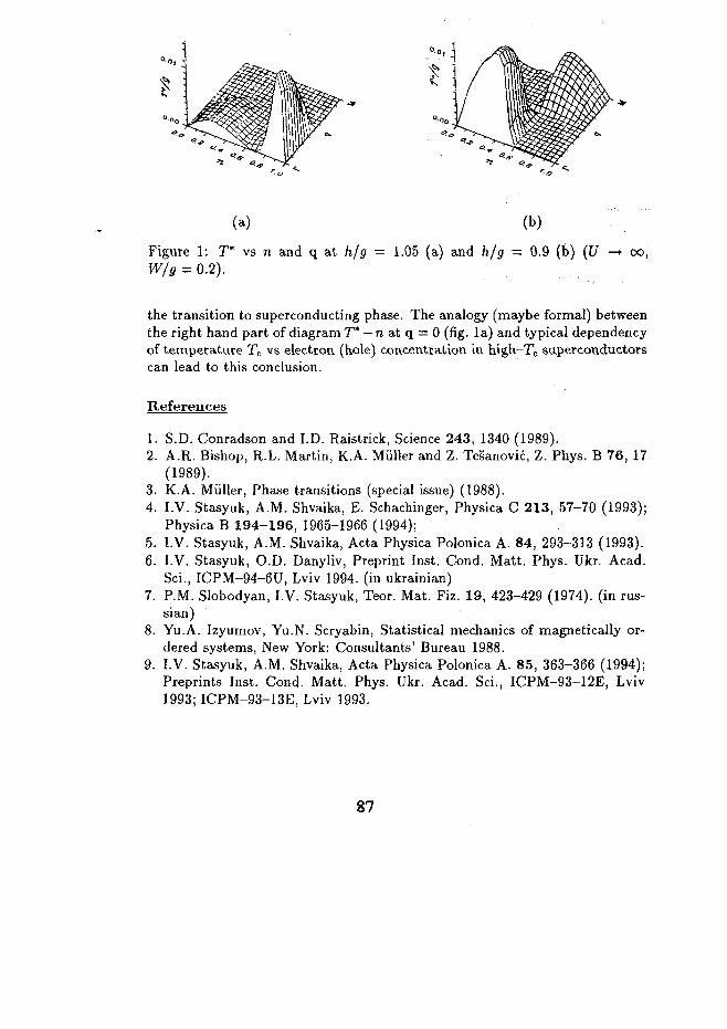
(a) (b)
Figure 1: T* vs n and q at h/g = 1.05 (a) and h/g - 0.9 (t>) (U -> oo,
the transition to superconducting phase. The analogy (maybe formal) betweenthe right hand part of diagram T* — n at q = 0 (fig. la) and typical dependencyof temperature Tc vs electron (hole) concentration in high-Tc superconductorscan lead to this conclusion.
References
1. S.D. Conradson and I.D. Raistrick, Science 243, 1340 (1989).2. A.R. Bishop, R.L. Martin, K.A. Miiller and Z. Tesanovic, Z. Phys. B 76, 17
(1989).3. K.A. Miiller, Phase transitions (special issue) (1988).4. I.V. Stasyuk, A.M. Shvaika, E. Schachinger, Physica C 213, 57-70 (1993);
Physica B 194-196, 1965-1966 (1994);5. I.V. Stasyuk, A.M. Shvaika, Acta Physica Polonica A. 84, 293-313 (1993).6. I.V. Stasyuk, O.D. Danyliv, Preprint Inst. Cond. Matt. Phys. Ukr. Acad.
Sci., ICPM-94-6U, Lviv 1994. (in Ukrainian)7. P.M. Slobodyan, I.V. Stasyuk, Teor. Mat. Fiz. 19, 423-429 (1974). (in rus-
sian)8. Yu.A. Izyumov, Yu.N. Scryabin, Statistical mechanics of magnetically or-
dered systems, New York: Consultants' Bureau 1988.9. I.V. Stasyuk, A.M. Shvaika, Acta Physica Polonica A. 85, 363-366 (1994);
Preprints Inst. Cond. Matt. Phys. Ukr. Acad. Sci., ICPM-93-12E, Lviv1993; ICPM-93-13E, Lviv 1993.
87

ELECTRON TUNNELING IN BI2223 UNDER HIGH PRESSURE.
V.Yu.Tarenkov, AJ.D'yachenko, A.V.AballoshevUA9600450
A.Galkin Donetsk Physicotechnical Institute National Academy of Sciences ofUkraine, Donetsk 340114, Ukraine
We have studied the electron tunneling in Bi2223 break junctions under highpressure 0<P<10 kbar. A reproducible pressure influence on the linear conductancebackground has been found. We observed, that the normalized conductance vsvoltage was increased with the pressure. This set of measurements seems to indicate,that the linear tunneling conductance may have its explanation in the characteristicsof the tunneling barrier namely on the resonant tunneling through the localized statesin the insulating barrier.
The Cu-O based superconductors were found to have the universal anomalies inthe tunneling conductance: for the NIN-junctions the dynamic conductancedl/dV=dI/dV(O)+yabs(V), where constant y depends on experimental conditions. Anumber of explanations for the unusual behavior of dl/dV in tunneling into the high-Tc supercondiictors has been proposed, including the voltage dependence of theelastic tunneling matrix elements [1], charging effects in the insulating barrier [2],and a modification of the effective tunneling density of states in terms of themarginal Fermi liquids theory (3], Kirtley et al [4] have argued that it may be clue toinelastic tunneling from a broad distribution of states. We may point, however, thatthe linear conductance background extends to the energies of eV-~0.5V [5] and more.that is beyond those of the elementary excitations, e.g. phonons, magnons. chargedensity waves that may be excited in the inelastic scattering.
An alternative approach has been developed by Halbritter [6], who showed theimportance of the contribution of localized states in runnel junctions. The localizedstates appear to be caused by title great number of defects, for example, by oxygendisorder in the Cu-0 chain region, which change the delicate hybridization betweenthe coper and oxygen levels. Both mechanisms of the linear contribution in to dl/'dVcan essentially distort the usual dl/dV-V parabolic dependencies for NIN runneljunction.
As is well known, the technique of liigh pressures is a powerful tool in the tunnelinvestigations [7], In our experiments it allows to separate the effects due to a changeof the tunnel density of states [3,4], inelastic tunneling [4.8] and the effects, whichare caused by the localized states [6].
The tunneling break junctions were prepared using small (0.02*0.5*10 mm) platesamples of Bi-2223 ceramic material with the optimal composition of
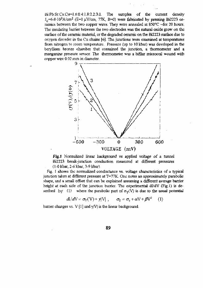
Bi:Pb:Sr:Ca:Cir-=1.6:0.4:1.8:2.2:3.0. The samples of the current densityJc=6-8-103A/cm2 (E=l aV/cm, 77K, B=0) were fabricated by pressing Bi2223 ce-ramics between the two copper wires. They were annealed at 850°C -for 20 hours.The insulating barrier between the two electrodes was the natural oxide grow on thesurface of the ceramic material, or the degraded ceramic on the Bi2223 surface due tooxygen disorder in the Cu chains [6]. The junctions were examined at temperaturesfrom nitrogen to room temperature. Pressure (up to 10 kbar) was developed in theberyllium bronze chamber that contained the junction, a thermometer and amanganine pressure sensor. The thermometer was a bifilar microcoil wound withcopper wire 0.02 mm in diameter.
-600 - 3 0 0 0 300VOLTAGE (mV)
600
Flg.1 Normalized linear background vs applied voltage of a tunnelBi2223 break-junction conduction measured at different pressures(1 -0 kbar, 2-6 kbar, 3-9 kbarY
Fig. 1 shows the normalized conductance vs. voltage characteristics of a typicaljunction taken at different pressure at T=77K. One notes an approximately parabolicshape, and a small offset that can be explained assuming a different average barrierheight at each side of the junction barrier. The experimental dl/dV (Fig.l) is de-scribed by (1) where the parabolic part of o"T(V) is due to the usual potential
dl/dV = crT(V) + y\,V| ,
bamer changes vs. V [1] and y|V| is the linear background.
* (1)
89

We have observed tlie strong pressure influence on the linear background term inthe normalized tunnel conductance cf=dI/dV. that is difficult to explain by the''marginal Fermi liquids effects" [3] or in the spirit of the theory ['!]. According to thetheory of inelastic tunneling [4] the changes in linear background are amount tochanges of the anfiferroniagnetic magnon spectral density F'.oV) and can no; beessentially.
30 -
K
b
10
-400
/ II
\
-200 0 200 100
U (mV)Flg.2 Normalized tunnel conduction vs applied voltage of a Bi222.'V)nmeasured at. different pressings (a- 9 kbai, b- 0 kbar>.
Sharifi et al. [9] formed the tunnel RKBO/Au junctions of vario\is resistances sothe change in the junction arrays was minimal. As a result, tliey have observed thatthe background slope y(P) was proportional to the zero-bias conductance rro(P) Wehave obtained another result: the linear background slope changed with pressuremore quickly than the conductance a 0 (Fig 1) For runnel junctions withtheconventional metals the pressure do not change the normalized tunnelconductance a f W a o , the obtained results demonstrated only a sensitivity of theasymmetry of conductivity o(V) to the applied hydrostatic compression (Svishmovet ai.[7]). As is seeii (Fig.2) for the Bi2223/In junction we have observed a stronginfluence of the pressure on the tunnel parabola.
To our mind there is only one main mechanism of the pressure influence on thelinear background: the change of the potential barrier height cp and thickness d underpressure. Really the tunneling into localized states is proportional to expt-dtp1'2') and
90

the conventional tunneling through ideal insulating layer is exp(-2d<pi/2). Thereforeafter the normalization process the contact conductance retains the exponentialbehavior with the tliickness d. .
This phenomenon have not been observed for tunnel junctions when barrier notcontains the localized states. In this case we have the equation (2), where o(v) is
o ( V ) / o ( 0 ) ~ N ( V ) (2)
conductance at the bias voltage v and N(V) is the density of states. The contributionto the pressure dependence of tunnel conductance arisen from the tunnel density otstates is small because according to the model [3] this contribution can be changedas the critical temperature Tc, but the observed dln(Tc>dP=0.002 value is too smallto explain the observed pressure effects.
Acknowledgments. , f
The authors are grateful to the State Committee on Science and Technology otthe Ukraine and to Prof. V.M.Svistunov for stimulating and helpful discussions.
References(1] J.R.Kirtley, Int.J.Mod.Phys. B4, 201 (1990)[2] S.Pan et aL Phys.Rev. B35,7220 (1987)[3] CM.Vaima and al, Phys.Rev.Lett. 63 (1989) 1996[4] J.R.Kirtley and D.J.Scalapino, Phys.Rev.Lett. 65,798 (1990)[5] V.M.Svistunov et al., Sov. Solid State Physics, 31, 296-299 (1989)[6] J.Halbritter Phys.Rev. B, 46, 14 861 (1992-11)[7] V.M.Svistunov. M.A.Belogolovskii, O.I.Chernyak, Usp. Fiz. Nauk. 151,31-66(1987)[8]V.M.Svistunov. l.lguchi, M.A.Belogolovskii, and A.l.Khachaturov,Mod. Phys. Let. B, 8 , 407 (1994)[9] F Sharifi. A.Pargellis, R.C.Dynes, Phys.Rev.Lett., 67,509 (1991)
NEXT PAGE(S)left BLANK
91


II. CURRENT TRANSFER
NEXTPAGE(S)left BLANK

UA9600451

MAGNETIC-FIELD AND DISPERSIONCHARACTERISTICS OF JOSEPHSON MEDIA.
L.V,BeIevtsov and S.S.ShevchenkoDonbas State Mashinbuilding Academy, 343916 Kramatorsk, Ukraine
As is well known, the current transport in Y-Ba-Cu-0 superconductingceramics has the Josephson nature. The disordered system of weak linksconsists of the contacts with the different critical current densities. Somewhatthese contacts can be destroyed with an increase in the transport current. Thatis why, the study of the self magnetic field which influences the intergraincurrent will be actual.
Another question is the correlation between the intergrain critical currentdensity and the grain size.
In this paper we consider the field and dispersion characteristics of the)Josephson system consisting of two grains. We assume the model is in thecritical state. We admit that the grain is of cylindrical geometry as well as thesmall size (i.e. a grain radius R « A:, with the A: is Josephson penetration
depth). As is shown in the inset in figure, the transport current J = (0,0,JZ)N
flows along the Z-direction, assuming that the external field is absent. J
Making use of the London (for grains) and Maxwell equations the followingrelation may be obtained for the average critical current density
<JC(H)>=JCO(1-H/HO) , (1)
where
I2
c"and A^ is the London penetration depth, Jco is the critical current density at
the temperature T = 0 and the magnetic induction H = 0. The dispersionfunction
271 AT
Ho = -=± P(y) Jco , y = R/AL , (2)
95
POO = v h(Y) / / tto0O- 1] xdx, (3)0
in terms of the modified Bessel's functions \v ( £ ). So, T = 77 K and
AL~ Kr5m, P(y) __ » 10, J c o « 10 I0A/m2 ,thenH0 == 1(T5T.y — 5
As appears from (1) - (3), the JC(H) function depends on:
(1) The grain shapes and sizes (R).
(2) The grain physical properties UL).
(3) The intergrain media properties (Jco).
(4) The self magnetic field (H).
Otherwise speaking JC = JC (H, R,AL,JC0)
It follows from obtained relation that if X\j* °o or R-> 0, then <JC> -» Jco.
But, if AL~* 0 o r R-> oo., then <JC> approaches to constant.
The figure shows the dispersioncurves for different magnetic fields
10'6T(2) and0"65 10"6T (3), as is computed from
eqs. (1) - (3). The stronger falldepending on < Jc(y) > is found for
the stronger fields and it characterizesthe beginning part of the curve. Next,with the growth of y the saturationbegins. This tendency shows, that thefine-grained ceramics is useful for us.
6 V
96
GIANT MAGNETOSTRICTION IN TEXTURED YBaCuOPLATES
V.V.Chabanenkoa, I.B. Krynetskiib, S. Piechotac andH.Szymczakc
a A.Galkin Donetsk Physico-Technical Institute, Donetsk, 340114, UkraineMoscow State University, Moscow, 117234, Russia
cInstitute of Physics, Warszawa, 02-668, Polandi IIIII mil
UA9600452The anisotropy of unusually large magnetostriction for textured YBaCuO wereinvestigated. The sample length change A L In the ab-plane when magnetic fieldH parallel and perpendicular to the c-axis were measured. Large jump of themagnetostriction coefficient assotiated with the flux jump were founded.
Magnetostriction measurements are a new technique for studies of themagnetic flux pinning as a fundamental property of real type-IIsuperconductors.
Studying Bi2Sr2CaCu20g single crystals, H.Ikuta et al. [1 ] reporteduncommon for superconductors high magnetostriction values, which can bequalitatively explained on the basis of the pinning mechanism for the magneticflux in the samples. High values of critical currents (80 kA/cm at 77K) inour MTG-samples stimulated us in our magnetostriction experiments.
For these measurements we used 0.5x3x5 mm3 melt processing YBaCuOplates. Variations of linear dimension of samples A L(H) = L(H) - Lo (whereLQ = L(H = 0)) in ab-plane was registered by a resistance tensometcr,incorporated in the branch of a dc-bridge. The rate of H variations alignedalong c-axes was8mT/sin the range ± 12T. Before every measurements thesamples were heated above the critical temperature.
In Fig. I field dependencies of the magnetostriction coefficient A L/Lo atdifferent temperatures for H orientation along c-axes are shown. At T=4,2Kif the field is increased up to 8T the sample is monotonously compressed andthen a avalanche-like (jump) variation of A L/Lo takes place associated withthe jump of the magnetic flux. After the jump of of the magnetostriction
97

is observed. After this in magnetic field 11 T the flux is again torn-off and thenafter some recpyer of dimensions a smooth change of the deformation sign upto 12 T takes place. Such jump phenomena associated with magnetotermicinstability were observed by us also in the magnetization. These data speak inthe favour of the magnetostriction mechanism based on the pinning [1,2].In accordance with [ 1 ] the equation of balance between the pinning force of aflux line f (on the unit of the length) and the internal local stress a (z) is writtenas follows:
da(z)/dz = N(z) fp, (1)
where N (z) - is the density of magnetic flux lines B (z). Sincef ~ dB(z) /dz, then from the balance equation (1) it follows that
(2)A L /LQ ~ 1/C j |BJ - B2(z)j dz ,
where C is the hardness coefficient, Ba is the external field and d is thethickness of the plate. Thus, variation of samples dimensions are given byvariations of magnetic flux distribution. The hysteresis of the magnetostrictioncoefficient (see Fig. 1) can be explaine by difference of distributions B (z) in theincreased and decreased fields.
In H 11 ab-orientation together with hysteresis phenomena in A L(H) consid-erable reversible variations of the magnetostrictioncoefficient are observed. Asfollows from the above data, the reversible part of magnetostriction is of hightemperature dependence. However, the irreversible phenomena in L(H) in thisorientation do not practically depend on temperature and have a complexform.
As follows from the measurements carried out and from the data taken from[3 ] the magnetic field as high as 8 T at 4,2 K produces in the sample pressureof ~ 0,5 kbar. Considerable external cyclic tensions can produce cracks insamples and thus decrease their current carrying characteristics. Sensitivity ofthe experiment allows to well register quite a few "creaking" impulses. It is tobe noted that these inpulses can be caused also by local lupms of the magneticflux.

- 3 . 5 •1 1 3 5 7 9 11Magnetic Field (T) Magnetostriction A L/LQvsH.
H II c,
7 § 4 6 4 , s nMagnetic Reid (T)
1. H. Ikuta et al. Phys. Rev. Lett. 70 (1993) 2166.2. M. Isino at al Phys. Rev. B 38, (1988) 4457.3. J.S.Schilling and S. Klotz, Physical Properties of HTS (ed. by
D.M.Ginsberg), 3, Singapore, 1992.

FLUX INSTABILITIES AND ANISOTROPY INTEXTURED YBaCuO IN THE STRONG MAGNETICFIELDS
V.V.Chabanenkoa, S.Piechotab, H. Szymczakb,E.M.Roizenblatc' S.I.Ermolinacand N.G.Kiselc
aA.Galkin Physico-Technical Institute of Ukrainian Academy of Sciences,Donetsk, 340114, UkrainebInstitute of Physics Academy of Sciences, Warszawa, 02-668, PolandLScientific and Research Institute of the Chemical Reactives and Materials forElectronic Technics, Donetsk, 340036, Ukraine
UA9600453Anisotropy of the development of instabilities in YBa2Cu307_<5 texturedsamples in magnetic field up to 12 T has been studied. Large jumps of themagnetic moment of the sample have been observed. Stabilization of themagnetic properties through remagnetization has been found out.
Progress in the HTSC technology resulted in creation textured samples, whichare usefull for technical needs. In this relation there is an increased interest instudying magnetodynamic instabilities in such objects [1-4]. The MTG-process results in a number of layered defects set in the ab-plane, in theformation of twins directed normal to the plane. These defects are theanisotropic centres of pinning and provide the anisotropy of instabilitybehaviour.
This report gives the results of investigations of anisotropy in the behaviour ofinstabilities in the magnetic properties of MTG-samples.
The magnetization M of the sample (1,5x1, 6x4, 2 mm ; jc(77K) =~ 80 kA/cm2 in the intrinsic magnetic field, Tc = 91,8 K) has been studiedwith the aid of the vibrating sample magnetometer. The rate of H change wasequal to 20 mT/s.
Initiation of instabilities for the samples with remanent magnetizationMrem > 300 emu/g in high enough fields is the well- known factor. Thus, forexample, in [3 ] for samples with M = 330 emu/g, at T = 6K, instabilities of
100

Hirr
co
C
o5
50
0
* ^ ™ ~ ~ - ^ _ ^
^ o ^ * * " ^
600
300
0
-300
-BOO0 4 8 . ^ 12Magnetic field (T)
8
4
0
-4
-8
0 4 8 y v 12Magnetic field (T)
b " ' } ' • • • - "
Fig.l. Magnetization vs H: (a) - H I I c, (b) - H I I ab.
the magnetic flux have been already observed in the H > IT oriented along thec-axes and expressed as nonrnonotous behaviour of magnetization M (H).In our samples possessing the helium temperature Mrem= 600 emu/g in thisorientation a large jump of magnetization has been observed (Fig la). Suchjumps of the magnetic flux accompanied by the development of instabilities
I 01

800'rfirst magnetizationsecond magnetization+Mmaxi
Fig.2.
Remagnetization curves.
-12 - 8 - 4 0 4 6Magnetic Field (T)
are typical of the type-II LTS (Evetts J.E. et al., 1964). Development of theseinstabilities can be explained by Mintz and Rakhmanov model.
One of the important experimental results is that in MTG-samples themagnetic-flux jumps at 4,2K take place only during the first magnetization andsubsequent first remagnetization of the sample after passing the maximum +Mmax (Fig.2). All other remagnetization starting from point - Mmax do not revelthe magnetic flux suppression, i.e. the total cycle of remagnetization as ifstabilizes the magnetic properties of the sample. Data of Fig.la evidence toothat at T = 46K, the hysteretic loop M(H) as a whole lowers down themagnetization axis, i.e. becomes "more diamagnetic" one. For field orientationalong the ab-plane at helium temperature the instabilities are absent (Fig. lb)which is evidently connected with a more than two time decrease of themaximum diamagnetic moment as compared with its orientation along thec-axis. But with temperature increase they occur in the form of giant non-monotonicities of magnetization with breaks (Fig.lb, T = 42K).
/. L. Legrand et al. Physica C 211 (1993) 239.2. A. Gerber et al. Physica C 209 (1993) 147.3.1. Monot et al. Supercond. Set Technol. 5 (1992) 712.4. K.-H.Muller and C.Andrikidis. Phys.Rev. B, 49 (1994) 1294.
102

UA9600454

MAGNETIC PROPERTIES OF TmBaCuO7_s 123 and YBaCuO8 124CRYSTALS
L.F.Cohen3, D.Laceya, G.Perkins3,D.Caplin3, Ming Xu", S.X.Douc,
S.A.Klestov ,V.l.Voronkova
a Centre for HTS, Blackett Laboratory, Imperial College, London SW7 2BZ, UK.
b Ames Laboratory, Iowa State University, Ames, Iowa 50011, USA.
c University of Woilongong, NSW 2500 Australia.
d Physics Department, Moscow State University, 117234 Moscow, Russia.
Magnetic studies of single crystals of HTS have been central in stimulating newideas relating to vortex phases and dimensionality. We have studied the form of themagnetic relaxation in high quality TmBaCuO 123 as a function of oxygenationand YBaCuO 124 crystals, for dc magnetic fields up to 8 Tesla, applied parallel tothe crystal c axis. In both systems similar regimes of vortex dynamics can bediscerned over a wide region of the H-T plane. We compare pinning properties inthe two systems as a function of reduced temperature and find the 124 systemapears to be considerably more anisotropic than well oxygenated 123.
IntroductionThe YBCOg 124 system is an interesting one to study magnetically because itshows no oxygen deficiency and does not form twin domains. Since it possesses adouble CuO chain structure it is instructive to compare its magnetic properties withthat of its sister compound YBCO.S 123 which has a single CuO chain only. It iswell known that the CuO chain in YBCO 123 plays a dual role[l]. Firstly, as acharge reservoir for the in plane superconductivity and secondly as an interplaneconducting link. The latter is responsible for the much lower anisotropy ofsuperconducting parameters in the YBCO 123 system compared to BSCCO 2212,for example. Although it might seem plausible that a second copper oxygen chainper unit cell would reduce the anisotropy further, this turns out not the case. Wehave studied the form of the irreversible magnetisation in high quality YBCO 124crystals and we make comparision with the behaviour of a series of deoxygenatedTmBCO7.s 123 crystals [2].
103

ExperimentAll experiments were carried out using an Oxford Instruments 3001 vibratingsample magnetometer with a 8T maximum vertical field. In this study we restrictour discussion to magnetic field applied parallel to the crystal c axis only.We define the irreversibility line (Hirr), as the collapse of the irreversiblemagnetisation or M-H loop. This evaluation is a function of magnetic field sweeprate and threshhold criteria. Although Hirr is rather ill defined a comparisonbetween different samples is still meaningful if the same criteria are used in eachcase. Where we discuss the normalised creep rate we refer to the change of themagnetisation signal as a function of the sweep rate of the magnetic field H'and wedefine the normalised creep rate to be S= dlnM/dlnH'[3].
Results and DiscussionWe first use the irreversibility line data to compare the behaviour in severaldifferent families of crystals. As oxygen is removed from the thulium samples theTc drops in a similar fashion to that observed for YBaCuO7.8 [2]. The Tc valuesvary from 91,88,84.8,82, 68.5, 57.8 to 56.5K. The BSCCO 2212 sample has a Tc'= 89K and the YBCO (124) a TC=85K. Figure 1 shows Hirr plotted against reducedtemperature t=T/Tc. We can see clearly the effect of deoxygenation in the thulium123 system and how it compares to the extremely anisotropic 2212 [4].Interestingly, the Hirr line for the 124 sample lies between that of the two thuliumcrystals which have a Tc of 82 and 84.8K (samples T4 and T3 respectively).
Figure 1: The Irreversibility field versus reduced temperature T/Tc for a series ofdeoxygenated TmBaCuOi.5 (123) crystals (+), an YBaCuOg (124) sample (0) anda BiSrCaCuO 2212 crystal (*).
104

We speculate that although 124 has two chains layers, its CuO2 plane-plane (or outof plane) coupling is weaker than well oxygenated 123 because of the greaterdistance between the planes. (The variation is from 8A in 123 to 14A in 124).Furthermore, as we remove oxygen from 123 we disorder the chains making the outof plane coupling weaker. The Hirr(t) in the BSCCO 2212 system is much lowerover much of the H-t plane than 123 or 124 and this is attributed both to weaker inplane pinning and out of plane coupling.As a result of this line of arguement it is interesting to compare the pinningproperties of two systems with chain layers whose Hirr(t) (for t>0.7), lie inapproximately the same region of the H-t plane, implying similar anisotropy values.In figure 2 we have made this comparison for the 124 sample withtC=85K and the123 sample (T4) with TC=82K at the same value of reduced temperature t = 0.5. Itcan be seen that the 123 crystal carries 30 times the current of the 124 crystalimplying that the in plane pinning in 124 is greatly reduced. We speculate that thisis a result of the absence of twin domains and oxygen disorder in the 124 system.
0E + 0 0 --0 2 3 4 5
Applied Field
Figure 2. The variation of the screening current density J with external magneticfield for the YBaCuOg 124 and the TmBaCuO6.7 123 crystal at the same value ofreduced temperature t =T/Tc=0.5. The latter shares the same Hirr (t) line as the124 sample but carries 30 times more current.
Next we look at the flux dynamics S (averaged for increasing and decreasing dcmagnetic field) in the 124 and T4 crystals. In order to compare the S behaviour inthe two systems using appropriate field scales [5] we show the correspondingmagnetisation curve M (in arbitrary units) on the same graph.
105

Cfl
0,042 4
Applied Field/T
Figure 3: The normalised creep rate S as a function of applied magnetic field atT=40K for the 124 crystal and T4, a deoxygenated 123 crystal with Tc = 82K. Inboth cases the magnetisation M is plotted in arbitrary units for comparison only.
We find for the 124 and 123 crystal T4, whose Hirr(t) lies in the same region of theH-t plane, rather similar behaviour both in the form of S as a function of magneticfield, and the absolute value. The 124 crystal has some extra low field feature in Sand M which has been associated with surface barriers[6]. We conclude that the inplane pinning properties which are quite different in these systems do not stronglyaffect the form of the flux dynamics.
References1. J.L.Tallon, 7th IWCC Austria, (1994). To be published, World Scienific.2. G. Perkins et al, to be published IEEE Trans, on Appl. Supercon. (1995).3. G. Perkins et al, submitted to Phys. Rev. B.4. L.F. Cohen t al, to be published in Physica C Dec. (1994).5. L.F. Cohen et al, Physica C 230,1, (1994).6. Ming Xu et al, Phys. Rev. B 48 10630 (1993).
106
DETERMINATION OF IRREVERSIBILITY LINEAND DISSIPATIVE LOSS IN YBCO FILMS
V.A.Khokhlov and V.F.Drobotko. UA96U0455A. Galkin Donetsk Physico-Technical Institute, Ukrainian Academy ofSciences, Donetsk, 340114, Ukraine.
The ac"susceptihility,,pf policristaline and epitaxial YBCO flliHs was*
investigated in exciting magnetic fields Hac = (' 0.1 - 1000 mOe) using the
inductance technique. The irreversibility line ('•' 1-Tm /Tc ) (Hac) and', the,n
maximum ofdissipativeios'ses% " (li.AC) were studied. Two characteristic fields
H* and H*2 with which ( 1-Tm /Tc ) fHa (J and x" (H&c) line than change
their slope were found. It was been shown that the index of degree at Ha c in
equation ( 1-Tm/Tc ) ~ a H^c depends.on a type of the weak links forming in
the YBCO film when it grows. .•-••.
One of the most important characteristics of high-Tc superconductors is the
irreversibility line, Tj^CH). This line separates the region of the reversible
behavior from irreversible one. Muller et-al. [1] found, measuring the
temperature dependence of the DC magnetization, that for bulk LaBaCuO
composites there existed in these materials a magnetically reversible region
above a magnetic field-temperature line between the lower and upper critical
magnetic field curves. The zero field cooled and field cooled magnetization
curves coincided in this region. They found that with increasing the applied
field H the certain lower temperature T ^ shifted according to
1-Tirr/Tc = aH q (1)where q = 2/3. They argued that this behavior was a consequence of asuperconducting glassy state.
Malozemoff et al. [2] found a similar relation in a single crystal of
YBa2Cu307 and called the new field-temperature relation the irreversibility
line. They have found that it could also be measured by the shift in temperature
of the peak of the dissipative susceptibility %" (T) with DC magnetic field.
107

Within the limitations imposed by the thermally activated flux creep modelused in they analysis, the irreversibility line is a crossover from flux creep toflux flow and not a true phase transition.
Alternative mechanisms have been suggested to explain the origin of theirreversibility line. These are vortex-lattice melting [3 ] and a phase transitionfrom a vortex glass to vortex liquid [4 ].
A detailed study revealed difference between the shift in temperature of thedissipative % " peak with DC and AC magnetic fields. The latter can bedescribed by the empirical expression [5 ]:
(1-Tm/Tc ) = [c list d jc(0) ] q x H!jc (2)
where d is the slab thickness, j c(0) is the critical current and T m is the
dissipative % '' peak temperature. The expression (2) describes the casewhen AC field parallel to the slab surface.
At the same time there was a report [6-9 ] that the irreversibility line does notfollow a power law (l)and(2)or that the exponent power q does not agree withthe theoretical values of 2/3 or 3/4.
In the present work we investigate the irreversibility line of epitaxial YBCOfilms using AC susceptibility measurements at exciting magnetic fields Ha c=
= 0.1-1000 mOe.There are three magnetic field regimes where the irre-versibility line and the dissipative susceptibility are quite different.
The diamagnetic susceptibility was measured at a frequency of 10 KHz bymeans of Hartshorn bridge, well balanced within a wide temperature range.The mutual inductance bridge was calibrated by the susceptibility measure-ments on a niobium film 0.1 mm thick whose shape was the same as that ofthe films studied. The apparatus and techniques for AC inductance measure-ments have been described previously [10 ].
The samples used in this study were prepared by the standart laser ablationtechnique on an StTiO3 (100) substrate. Thefilmthicknesswas0.3mm. X-rayanalysis has revealed that the films were single phase (100 % YBa2Cu307x).The scanning electron micrographs of this films indicated that the averagegrain size is of the order of 1 mm and the connectivity between the grains
108

appears to be fairly good, with no gaps arid that these often from clusters ofthe size of 0.1 -1 mm. Details of preparation methods can be found in ref. [11].
The irreversibility line is determined from of the imaginary (£ " ) part of the
AC susceptibility at different exciting magnetic fields.The irreversibility
temperature is defined as the peak temperature T m of the# ".. versus T
curves, that is T i r r = T m [12 - 14 ]. The dissipative loss curve % " (T) at the
ultraweak magnetic field 0.2 mOe has a fine structure - five of the dissipative
X " peaks. The width of the dissipative peaks is increased with increasing the
AC field, they are merged and a single peak is only observed at H a c = 1 Oe.
At these magnetic fields a good match between the hysteresis losses % "
(Hac) and the shift.in temperature of the# " peak in the low temperature
region has been obtained. As shown in Fig.l, there are three differentmagnetic field regions: from 0.2 to 5 mOe, from 5 to 100 mOe and up, to 100mOe. At H a c up to 100 mOe the diamagnetic response can be described with
help to the critical state model. The local value of the macroscopic currentdensity induced in the film is given by
j = j c (0) { 1 - (kT/U) In (cE / 2 K VO B)} . (3)
0.20
0.15 -
O
"X
> o.io -
"x
0.00
. - - - • — * •
• * - , -
si-0.015
0.0S 1 f /
H2* j H t = 9 0 mOe
YBCO #364
o.6o
0.020
£Fig.l
-0.009
0.000
(Oe)" 2
109

where K is the average distance between the pinning centers, v0 is thefrequency of the vortex oscillation in potential well and U is the well depth [12].In the magnetic field region from 5 to 100 mOe there is a transition from a lowto strong flux creep. The slope of the irreversibility line in such fields varieswith decrease of the critical current density. We assume that in a weakmagnetic field the pinning potential is decreased with increasing thetemperature. As a result, the viscous motion of vortices is decreased and thevortex lattice is melted. The hysteresis losses are drastically reduced.The existence of the gigantic flux creep can be the reason of the independencetemperature range on a magnetic field-temperature line in ultraweak ACfields. This assumption confirms of the anomalous behavior of the lower criticalcurrent H c j in a narrow temperature range around T = 85.8 K, asillustrated in Fig.2.
In the magnetic field region from 0.2 to 5 mOe we found the linearity of thediamagnetic susceptibility of the film. Previously, we reported that thelinear diamagnetic response had nothing common with the critical state [IS].
The most interesting information about films has been obtained when filmswere exited by a very weak magnetic field « 0.1 to 1 mOe. The diamagneticresponse in such fields develops in a narrow temperature range around T .
c
1U ;
CO io*i
ri
m 10:
i:
10"-YBCO { |l 364
k
Fig.2
T, K
no

'Owing to this we have observed the change in the motion mechanisms 6fvortices in three magnetic field regimes. It is suggested that the exponent powerq in empirical expression (2) depends on type of the weak links forming inthe film during growth.
Acknowledgments. This work was supported in part by Soros Foundation grant(UG 334) awarded by the American Physical Society, by the Ukrainian StateCommittee for Science and Technologies (project "Control" and "Network").The authors also with to thank Dr.A.I.D'yachenko and Dr.Yu.V.Medvedevfor their valuable discussions.
/. K.A.Muller, M.Takashige, J.G.Bednorz, Phys.Rev.Lett 58, 1143 (1987).2. Y. Yeshurun, A.P.Malosemoff, Phys.Rev.Lett. 60, 2202 (1988).3. D.R.Nelson, Phys.Rev.Lett. 60, 1973 (1988).4. P.A.Fisher, Phys.Rev.Lett. 62, 1415(1988).
5. A.P.Malozemoff. in: Physical Properties of High-TemperatureSuperconductors, D.M.Ginsberg (ed.), World Scientific, Singapore-NewJersey-London-Hong Kong (1989).
6. C.C.Almasan, CL.Seam.an, Y.Dalichaouch, M.B.Maple, PhysicaC 174, 93(1991).
7. J.CGarland, C.C.Alsman, M.B.MariePhysica C 181, 181 (1991).8. A.Hammer, G.Srinivasan, J.Appl.Phys 69, 4899 (1991).9. A.A.El-Abbar, P.J.King, K.J.Maxwell, J.R.Owers-Brandley, W.B.Roys,
Physica C 198, 81 (1992).10. A.M.rpHinHH, B.O.flpoooTbKO, B.fl.OracoBCKHH, B.A.XOX^OB, 5KT<D, 63,
190(1993).11. V.G.Prokhorov, V.I.Matsuy and B.A.Vas'ko, Superconductivity 5, 505
(1992).12. A.N.Artemov, V.F.Drobotko, D.G.Emel'ynenkov et al., Phys. Lett. A
157,85(1991).13. A.M.Grishin, V.F.Drobotko, D.G.Emel'ynenkovet al., Superconductivity
5,290(1992). , '14. A.M.Grishin, V.F.Drobotko and V.A.Khokhlov, Superconductivity 5, 648
(1992).15. A.M.Grishin, V.F.Drobotko, V.A.Khokhlov et al., Low. Temp. Phys. 19,
930(1993).
I l l

DOUBLE-STEP BEHAVIOR OF THE CRITICAL CURRENT VSMAGNETIC FIELD IN A METAL CERAMIC: infergranular fields andrelaxation
A.l.D'yachenko UA9600456A.Galkin Donetsk Physicotchnical Institute National Academy of Sciences ofUkraine, Donetsk 34114, Ukraine.
A theoretical analysis of metastable states for the flux line lattice at thevacuum- superconductor interface have been performed. A new model is describedthe physics of a strong magnetic field H influence on the critical current Jc ofthe anisotropic high- Tc superconductors.
It is known that the magnetic field H considerably influences the critical current Jc
of a system of superconducting grains coupled by Josephson weak links (the"Josephson medium"). It turns out, however that the situation changes considerablyif vortices have entered into the granules. If the field H is parallel to the contact areathen intragranular vortices reduce the surface current Jsf of the granules and hencechange the sensitivity of Josephson junctions critical current on the field H. In themost general case the JC(H) value is determined by the magnitude of a surfacecurrent Jsf, Jc(H)~l/Jsf(H). The basic idea of the model [1,2] is that the Jsf value isthe sum of "Meissner" component Jm and the irreversible critical current ofgrains J c g [1 ], Jsf=Jcg^Jra, and
Jc<Ky-JC0/{\+q(2k (Jcg+Jm)+Hxt)), (I)
q=27ija0 r /O 0 , r is the "short Josephson junctions" width, t is the Josephson contactthickness, X. is the London penetration depth into the granules H is the fieldcomponent parallel to the contacts plane. The value of surface current J in canbe equal to the Ginzburg-Landau decoupling current J ^ only for H>HC andvery uniform superconductor/vacuum (S/V) interface, when the situation withthe Bean- Livingston surface barrier is realized (here Hc is thethermodynamic magnetic field. H c » H c j ) . For a nonuniform S/V interface theMeissner state becomes unstable for H>Hcj at a "weak place", where the value ofthe surface current Jm is close to J^c. But out of the surface defects the localvalue of the surface current Jm(r) is regulated by small elastic deformations of theflux line lattice. Let us assume that this process realizes in accordance with theknown principle of minimum entropy production. In that case, almost on the wholesurface of the superconductor the flux line lattice is in a metastable state with theminimum possible "Meissner" current Jm= Je c= Hc\/\«i^c, -consequently, if

the vacuum- superconductor mterface is nonuniform almost on the whole surfacethe condition >ni=JSq is fulfilled. Once the flux line have penetrated into theJosephson junction banks, an addition surface current component J c g appearswhich is caused by the gradient of the density of these vortices, whereas theamplitude of the Meissner surface current J^ is controlled by the induction Bjump at the S/V interface. In an increasing magnetic field H u p , the vortex densityinside the grains is less than at their periphery, so that Jc g sums with Jm:•}si^up)~= •'m : hg>- l n decreasing field H(}o w n tlie total surface current densitydecreases, Jsf{down>=Jm(down)-JCg.
If there exists a Bean- Livingston surface barrier to vortex motion theequilibrium par! J in for field increasing and field decreasing processes isextremely different and, as a result, the strong hysteresis of the Josephson criticalcurrent Jc exist: Jni(up)/Jm(down)~Hc/Hcj».l (!]. On the other hand, whenthe vortices penetrate into the granules the surface current Jsf(up) isapproximately constant and the Josephson medium critical current Jc vs. Hdependence has a double- step behavior (2]. The first drop in Jc is for H<Hcj(H<kHc for the;Bean-Livingston surface barrier, k<l). This is followed by aplateau region of relatively constant critical current at magnetic fields H<Hjj.,where the Josephson medium irreversibility field Hj,- is
Hil.=(2X/t)(Hc!! 1 + A/f) + XJcg) . (2)
In the framework of the discussed model, reason for the Jc vs. H hysteresisbehavior lies in the irreversible dependence of the granules surface current. Anadditional contribution arises if the dipole field of the grains H r e v (or persistentloops) changes the intergranular field value Hg [3].
Let HU]f is tlie internal field, H e x is the external field and B a v is the averageinduction field in the sample. Then
f H r e v - Hex+(Dg-D)xMay+H r ev , (4)
where D, Dg are the demagnetizing factors of the whole sample and of theaverage grain respectively, Mav=Mav(Hjnt) is an average magnetization of theJosephson media and H r e v is the dipole field of the grains (or persistent loops)which spills into the intergranular region, Hrev=-kgMg, for Mg~±y<a>JCg is thegrain magnetization for the intragrain critical current lcs and grain diameter <a>^y~l.The average induction field B a v is related to the field within (subscript s) andbetween the granules ("subscript n) by . ... - ,;,,
113

Bn> = £;(Hg+Mg+Meq) + (l-f s)Hg-Hg+f sxM) , (5)
frpl-fs, M(Hgr)=Meq+Mg is the full grain magnetization, Meq is theequilibrium part of the grain magnetization, Meq~ -H c j g . From (3-5) one obtainthe relation between internal Ho and applied HgX fields
Hg= HeX + {(Dg-D)xfsxM + (l-D)xHrev}/(l-Dg) . (6)
The average field along the grain boundaries (6) can be approximated by
Hg=Hex - nxM(Hg), (7)
where n is the effective demagnetization factor of the grains in the granular sample,
n={(D - Dg)xfs+(l-D)xkg)/(l-DgKO . (8)
For a granular film in the normal external field D~l, Dg~l/3 and n~fs, Hg=Hex-fsxM. For a thin slab in the parallel field D ~ 0 and
ri=-!'Dgxfs-kg)/(l-Dg).
Recently, Kwasnitza and Widmer have found, that the relaxation rate of theintergrain critical current Jc is strongly hysteretic[4]. They take on trust that the valueJc is determined by the effective field Hg between the grains. This effective field is asuperposition of the applied field H e x and the field B m due to the magnetization ofthe grains [3]. At first sight, this simple model is evident. Unfortunately, this model isunrealistic. As is seen from (7-9) in the very experimental situation effectivedemagnetizing factor n <1 and at high fields and low temperatures intragrainvortices in the closer vicinity of the Josephson junctions strongly influence theJqsephson current and are responsible for the high- field hysteresis behavior of Jc.The grain demagnetization effect (7) undoubtedly plays a secondary role at thesefields.
According to the model [1,2] even without grain demagnetization, theirreversible flux dynamics inside grains should contribute to the irreversible behaviorof Jc. The reason is that the intragranular critical current density. Jc g at the grainsurface adds to or subtracts from the Meissner shielding current. With me knowledgeof the hysteresis of intragrain current JCg relaxation is it now possible to makedetailed predictions on how the critical transport current Jc should change in time.
114
The critica] current of a Josephson contact Ic in the parallel field H can be writtenin the following form Ic(H}=ffHef|(H)), where f(H) is given by the real structure oft h e c o n t a c t a n d • • • • • • • .-
In the Meissner phase of grains the surface current density Jsf is Jsf=H/A,, soHej=f=H. For the derivation of the transport-current relaxation Jc(t)~Ic('c) we find thederivative
d/( ;Jc(x))/dA={di(Jc(H))/dH} x {dH/dHeff} x
In the mixed state dHefj/d/T=+(2A.2/t)x{dJcg/d/t}, Jcg=yt<a>Mg? and at least
d/«Jc/d/x=±{2X2/7t<a>}x{d/«Jc/dH}exp{dM7d/x}exp; ... (9) .
where the derivatives {d/«Jc/dH}cxp, {dM/d/x}exp are the experimental values, (+),.corresponds to the increasing and (-) to the decreasmg external field H. According to(9) the relaxation rate of the critical transport current is strongly hysteretic. As afiinction of the external magnetic field cycling the Jc relaxation rate dJc/dx can bepositive or negative and even equal to zero.
In summary, we favor the idea that hysteretic behavior of criticalintergrain current JC(H) is caused by the change in the direction of ihsintTagranular critical current density Jcg. Usually the plateau in JC(H) is explainedby current percolation through weak link free paths [5]. We argue that this high fieldbehavior is also consistent with Josephson coupling of grains that are in the mixedstate. The thermally activated motion of the vortices in the grains should be reflectedin the surface current what turns in the transport current Jc(H)=Jc(Jm±JCg). Thisnovel flux creep effect is a result of the decay of the induced intragrain current JCgand supports the proposed model.
Acknowledgments. The work was supported by the State'Committee on scienceand Technology of the Ukraine.
References . .1 A.I.D'yachenko, Physica C 213,167(1993)2 A.I.D'yachenko, Mod.Phys.Lett. B, 8,N17 (1994)3J.E.EvetsandB.A.Glowacki,Cryogenics,28,641(1988)i.4 K.KwasmtzaandCh.Widmer, Physica C 202; 75 (199^) "-.5 J.V.Ekm, H.R.Hart and A.R.Gaddipati, J.Appl.Phys..,68,2285 (1990)
115

UA9600457
EFFECT OF SUBSTITUTION OF Hg FOR Cu ON PROPERTIES OF Hg-BASED HTSC.R.V. Lutsiv, Yu.N. Myasoedov, M.V. Matviiv, Ya.V. BojkoHTSC Laboratory, Dep. of Phsics, Lviv State University, Lviv, UA-290005,UKRAINE
New Hg-based HTSC are synthesized in a homological series ofHgBa2Can_1CarP2n*2+5i w e r e n > 1 a n d 5 - excessive oxigen in a Hg-plane [1-5J. Analogously to Tl based HTSC, number of CuO2 layers per elementarycell in the Hg-based HTSC grows with increase of n and the temperature ofsu-perconductive transition Tc increases for 3>n>1 The Tl- and Hg-seriesdiffer in oxygen occupancy of a site in Tl - or Hg-plane, what is greater then0,75 in the Tl-compound [6,7], but is significantly less than 0,5 in Hg-basedsuperconductors [8,9], In contrast to Tl-based HTSC, a HgOs plane in the Hg-based HTSC in larger extent is depleted by oxygen, were uniqueproperties of dependence of Tc on pressure are observed for 0,25<5<0,4[10-12]. Maximal reached Tc=164K has been obtained for Hg-1223 underpressure of 100GPa [12]. For low temperature phase of this HgBa2Cu)4+5
(n=1, Hg-1201) series, the temperature Tc is changed reversibly with 5 fromOK in underdoped state (5=0; dielectric) to 97K (8=0,25; peak) and furtherit is decreased to 20K (5=0,4; overdoped state) [13-15]. The structure of Hg-1201 represents by itself a sequence of layers(CuO2)(BaO)(HgOs)(BaO)(CuO2), were Cu cations are octaedricallycoordinated but coordination of others cations depends on value of oxigenindex 5. As the excessive oxigen atoms increase the average oxidation rateof copper and create the concentration of holes necessary forsuperconductivity, then one can expect that the change of Tc is bound upwith the extent of filling of possible positions in Hg-plane by oxigen atoms.J.L.Wagner for the first time has observed, that 5 is changed depending onoccupation of (1/2 1/2 0) position in Hg-plane by the oxigen atoms (0,08 performula unit) [8]. It was noted, that the substitution of some Hg for Cu at (0 00) position can initiate additional oxigen in (1/2 0 Z) position. At the sametime the autors have not noticed in the samples studied the change ofconcentration of this defects type depending on an annealing conditions, andits contribution in doping has remained unclear.
In our papers [16,17], it was set forth an assumption, that creation ofsuffitient number of defects of substitution of Hg for Cu together withadditional oxigen in Hg-plane at (1/2 0 0) position should result in the holesconcentration increase and respectively in the Tc increase. In papers ofL.W.Figner and O.Chmaissem [18,19] one can find confirmation of influence
116

UA9600458

of excessful oxigen at different positions on SC-properties. Samplescorresponding to nominal stoichiometry of Hg-1201 have been prepared in atwo-step process as described in reference [1,16,17]. After synthesis, smalldrops of Hg were observed in a quartz tube. At the same time X-ray powderdiffraction analysis gives evidence of possibility of substitution of Cu for Hg.In Table 1, there are characteristics of two samples with different levels ofsubstitution of Hg for Cu. Occupancy of (1/2 1/2 0) position for(Hg089Cu011)Ba2CuO4+5 and (1/2 0 0 ) one for (Hg083Cu017)Ba2CuO4+6 with
the oxigen results in considerable differences in SC-properties.The temperature dependences of second harmonic generation and magnetic
susceptibility are shown in Fig. 1 and the values of Tc equal to 94K and 120Kfor the (Hg089Cu011)Ba2CuO4+5 and (Hg083Cu017)Ba2CuO4+5,correspondingly, were found from comparison of these dependences.Schematic representation of an elementary cell for different levels of fillingby oxigen of position in Hg-plane is shown in Fig.2. The difference inproperties between the three mentioned states is defined by coordinatecharacteristics of positions of statistical mixture H g i ^ C u ^ . Stoichiometric
defectless HgBa2CuO4 (81=82=5=0) is a antiferromagnetie insulatoraccording to the Mott-Habbard description as well as others undoped cuprates(e.g., La2CuO4 and (Sr,Ca)CuO2) . Filling of positions (1/2 1/2 0} with oxigenfor (Hg089Cu011)-1201 results in appearance of SCrproperties. For exceptthe filled to 78% atomic positions 01, corresponding to the"dipole"surrounding of the Hg atoms it appears that,-the one of possibleintestitial positions (1/2 0 0) is filled fo 26%, providing with general octahedralcoordination at joint presence of all oxigen atoms at (0 0 0..221) and (1/2 0 0)positions in elementary cell. The presence of statistical fragments withquadratic (octahedral, see Fig.2c) coordination of Cu in addition to basiclayers of squares [CuO2], i.e. the presence of two layers [CuO2] in averagedelementary cell, allows to explain characteristic for two-layered by [CuO2]structures increase of Tc from 94K for (Hg089Cu011)-1201 to 120K forO~'9o83(-'U0 17H201. Defects of substitution of Hg for Cu is the necessarycondition of the structure stabilization and together with additional oxigen atposition (1/2 0 0) affords the increase of the hole concentration and density ofstates near Fermi level. As a concequence of this, it is the increase of Tc.
Increasing of Tc to 118 K under pressure for Hg-1201 [19] gives evidence ofpossibility of Tc increasing also at "chemical" compresssion. Complex studyof the substitutional defects Hg/Me will reveal directions of search of newHTSC.
117

160
Fig.1. Temperature dependence of SHG and %ac for t w 0 different states of
oxidatort Hg- states of oxidaton Hg-1201 : o -(Hg089Cu011) - 1201, with theposition (1 /21 /2 0) which is occupated by the atom of oxigen and o -(Hg083Cu017)1201 with the position (1/2 0 0 ) which is occupated by the
atom of oxigen respectivrly. In the inset we plot p(T) for (Hg089Cu011) -1201.
118

CuO
Fig.2.Schematic representation of an elementary cell for different levelsof filling by oxigen of position in Hg-plane. .;••
Tabl.1. Coordinates and isotropic thermal parameters of atoms in the(Hgi.6lCu51)Ba2CuO4+sl^2
8 =(ATOM X YHgCud
BaCuO(1)O(2)O(3)O(4)
0 00 00.5 0.50 00.5 0.50 00.5 0.5-
0,11Z
000.2970.500.2090-
Sites occupationsa) Hg:d)O3: i
N0.89(1 )a)0.11(1)a>2122Id)-
0.89(1)Hg+0.11(1)Cu; b)0.12(4)0 e)O4 : 0,24(9)0
B(is/eq)1.45(4)-0.96(3)0.81.(7)0.5(3)1.2(3)1.160-
X000.500.50-0,5
Y000000-
0
Hg: 0,83(2)Hg+0,
8=0 ,
z00
.5 0.2940.5
.5 00.221-0
17(2)Cu
17N
0.83")0,17b)21202
-2e)
c) O1:
B(is/eq)1.0(2)-
1.2(1)1.5(8)1.5801.580-
1,580
0,78(9)0;
119

-*[1 ] S.N. Pu|Jlin , E.V. Antipov , O. Chmaissem & M. Marezio, Nature-362,226(1993).
[2] R.L. Meng, Y.Y. Sun, J. Kulik, Z.J. Huang, F. Chen, Y.Y Xue & C.W.Chu, Physica C 214, 307.(1993).
[3] A. Schilling, M. Cantoni, J.D. Guo & H.R.Ott, Nature 363, 56 (1993).[4]S.M.Lourairo, E.V.Antipov, J.L.Tholence, J.J.Capponi,
O.Chmaissem, Q. Huang & M. Marezio, Physica C 217, 253 (1993).[5] E.V. Antipov, S.M. Lourairo, C. Chaillout, J.J. Capponi, P. Bordet,
J.LTholence, S.N. Putilin & M. Marezio, Physica C 215,1 (1993).[6] S.S.Parkin, V.Y.Lee, A.I.Nazza, R. Savoy, R. Beyers and S. LaPlaca,
Phys. Rev.Lett., 61 (1988).[7]R.M.Hazen, in Physical Properties of High Temperature Supercon-
ductors, ed. D.M.Gindzberg, 2, 121 (1990).[8]J.LWagner, P.G.Radaelli, D.G.Hinks, J.D.Jorgensen, J.F. Mittchel,
B. Dabrowski, G.S. Knapp and M.A. Beno, Physica C 210, 447(1993).
[9] O.Chmaissem, Q.Huang, E.A. Antipov, S.N. Putilin, M. Marezio,S.M.Loureiro, J.J.Capponi, J.L.Tholence and A.Matoro, Phys. C217, 265 (1994).
[10] B.A.Hunter, J.D.Jorgensen, J.LWagner, P.G.Radaelli, D.G.Hinks,H. Shaked and R.LHitterman, R.B.Von Dreele, Phys.C 221,1 (1994).
[11] A.I.D'yachenko, V.Yu.Tarenkov, A.V.Abalioshev, R.V.Lutsiv.Yu.N.Myasoedov and Ya.V. Bojko, Phys. C (to be published).
[12] J.H.Eggert, J.Z.Hu, H.K.Mao and L.Beauvais, R.L.Meng, C.W. Chu,Phys. Rev. B 49, 15299 (1994).
[13] Y.Y.Xue, Q.Xiong, F.Chen, Y.Gao, L.M. Liu, A.J. Jacobson, C.W.Chu, Preprint No 94:055, Houston, Texas.
[14] Q.Xiong, Y.Y.Xue, Y.Gao, F.Chen, Y.Y.Sun, Y.Gibson, L.M. Liu,A. Jacobson, C.W. Chu., Preprint No 94:022, Houston, Texas.
[15] Q.Xiong, Y.Y.Xue, Chen, Y.Gao, Y.Y.Sun, L.M. Liu, A.J. Jacobson,C.W. Chu., Preprint No 94:054, Houston, Texas.
[16] R.V.Lutsiv.Yu.N.Myasoedov, I.V. Kityk et. al, FNT, 20, 6, 606 (1994)[17] Yu.N.Myasoedov, R.V.Lutsiv, I.V.Kityk et.al, to be published in the
Vll-Evrophys.conference of material EURODIM-94, France (1994).18] L.W.Finger.R.M.Hazen, R.T.Downs, R.L.Meng, C.W.Chu, Physica C
226, 216(1993).[19] O. Chmaissem, L. Wessels, Z.Z. Sheng , Phys. C 231, 216 (1994).
120

ABOUT THE ROLE OF SILVER IN HIGH TEMPERATURE REACTIONS OF YjBa2Cu3O7 .8
SUPERCONDUCTOR CERAMICJorge E. Fiscina1-2. Carlos J.R. Gonzalez Oliver2, and Daniel A. Esparza1. Centra Atomico Bariloche (CNEA). 8400S.C. de Bariloche (RN). ARGENTINA. (1) Comision, Nacional de Energia Atomica. (2) Consejo Nacional deInvestigaciones Cientificas y Tecnicas.
^Superconducting properties vs. firing protocol was studied in Ag-YiBa2Cit3O7^ composite. We present. as a part of a
jiiore complete study, R vs. T characterization, DTA-TGA measurements, and SEM-EDAX analysis^Silver affects the high temperature reactions of YjBa2Cu-^O7_5 ceramic, shifting the on-set temperature of reaction,
and changing its dynamics. The central rol of Ag-AgO eutectic temperature in the thermal behavior of Ag-YjBa2Cu3O7_g cermets was established. At pre-Ag-AgO eutcctic temperatures, silver increases the partial
decomposition of !23 phase, while at post Ag-AgO eutectic temperatures, we note a optimal re-absorption of the 123acompanying phases. In this range of temperatures, a modified 123 phase, named 123 , is re-assembled in the 123grain boundary region. R-T characterization show us for the 123 an on-set critical temperature of 95K, and from XRDanalysis an increased c-axis.In particular, we deduced from SEM-EDAX that the liquid post-peritcctic was modified. We can observe that theprocess of nucleation and growing of the 123 phase was more efficient in the silver doped ceramic, it means a betterreabsorption of 123 acompanying phases (ie.:011).
Synthesis of Ag-Y]Ba2Cu3O7_§ cermets allows the obtainement of a material with superconducting state performance
that is specially apt for specific applications (i.e.: superconducting wires and tapes). This work is a part of a completestudy*'2 of the role of silver in the interaction between 123 phase with its accompanying phases.Here in, we present DTA-TGA experiment on a Ag plus YiBa2Cu3G"7_§ homogeneously mixed powder', under
dynamic Oxygen atmosphere, with constant heating rate of 10°C/min. The cycle consisted of heating from ambienttemperature up to 1200°C, and cooling till around 400°C.In order to carry out R-T characterization and SEM-EDAXmicrostructural analysis vs. thermal protocol, we treated by differnt sintering paths, pellets from the Ag plus
_§ powder1.
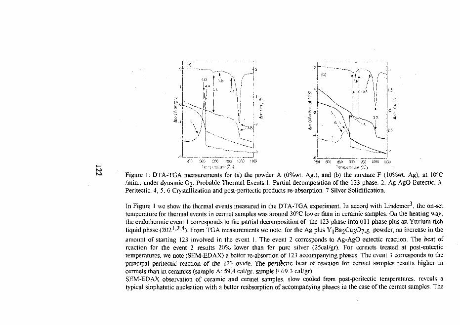
toto
750 800 8W) 900 960 1000 1050
Figure 1: DTA-TGA measurements for (a) the powder A (0%wt. Ag.), and (b) the mixture F (10%wt. Ag), at 10°C/min., under dynamic 02- Probable Thermal Events: 1. Partial decomposition of the 123 phase. 2. Ag-AgO Eutectic. 3.Peritectic. 4, 5, 6 Crystallization and post-peritectic products re-absorption. 7 Silver Solidification.
In Figure 1 we show the thermal events measured in the DTA-TGA experiment. In accord with Lindemer-', the on-settemperature for thermal events in cermet samples was around 30°C lower than in ceramic samples. On the heating way,the endothermic event 1 corresponds to the partial decomposition of the 123 phase into 011 phase plus an Yttrium richliquid phase (2021'2-4). From TGA measurements we note, for the Ag plus Y j I ^ C ^ C ^ s powder, an increase in theamount of starting 123 involved in the event 1. The event 2 corresponds to Ag-AgO eutectic reaction. The heat ofreaction for the event 2 results 20% lower than for pure silver (25cal/gr). For cermets treated at post-eutectictemperatures, we note (SEM-EDAX) a better re-absortion of 123 accompanying phases. The event 3 corresponds to theprincipal peritectic reaction of the 123 oxide. The peritectic heat of reaction for cermet samples results higher incermets than in ceramics (sample A: 59.4 cal/gr. sample F 69.3 cal/gr).SEM-EDAX observation of ceramic and cermet samples, slow cooled from post-peritectic temperatures, reveals atypical sinphatetic nucleation with a better reabsorption of accompanying phases in the case of the cermet samples. The

presence of ~3(.im silver grains array on a 123 ceramic-pseudograin matrix, the event 7 (figure 1 (b)) of a 21 cal / grcorresponds to silver segregation and solidification, and it is an evidence of the Ag-. Ba-, and Cu- liquid compoundexistence at postperilectic temperatures. From etching studies on these samples, it was concluded^ that in the presenceof silver the 123 grain boundary is formed with_a lower interface solid-solid energy.
Figure 2: R-T behavior of 123 Ceramics, and 123-Ag Cermets vs. sintering paths in Oxygen dynamic atmosphere(except M120: in Air): M112A (SSC+6%wt. Ag Flakes): s 9()0°C, 10 hs.. M117A (SSC+6%wt. Ag Flakes). Ml 18(SSC+6%wt. Ag JM), y Ml 19 (SSC): s 930°C, 40 hs.. M120 (SSC+6%wt. JM): 932°C. 17hs.. M135 (SSC+3%wt. AgFlakes), y M137 (SSC+6%wt. Ag Flakes): s 950°C, 20hs.

In figure 2, we show the R-T characteristics vs. different sintering paths. The experiment of the figure 2 (a) shows theeffect of the endothermic event 1 on the transport properties, because of the 011 phase precipitation at the 123 gTainboundaries zones, i.e.: cermet Ml 12 was sintered at 900°C that correspond to the beginning of the event 1. CermetM117A was treated first at 93O°C, that is around Ag-AgO eutectic temperature, and in a second treatment, the samesample was treated at the event 1 on-set temperature (~900°C) for obtaining the cermet M117B. SEM-EDAX analysisshow us, a good densificated cermet Ml 17A, with 123 grain boundaries zones free of accompanying phases. Thiscontrast with the 011 zones between 123 grains for sample Ml 17B. We noted through chemical etching technique, thehigh degree of crystallinity of 123 grain couplings. M117A and B microstructural aspects correlate with a sharptransition R-T behavior for sample M117A (Figure 2(a)), that it was degraded after the second treatment (sampleM117B). In Figure 2 (c) we show R-T characteristics for ceramic and cermet samples treated at 930°C, the high silverdiffusivity at this temperature promotes for cermets a sharp transition behavior.Figure 2 (d) shows the R-T characteristics for cermets M137 and Ml35 treated at 950°C, for these samples the on-settemperature for the normal-superconductor transition was around 95K. An XRD analysis on these samples show us atendency in 123 phase c-axis to be longer than in 123 phase treated without silver.We can conclude that the Ag-AgO eutectic reaction is central to clarify the rol of silver in these cermet system. While atpre-eutectic temperatures silver promotes the partial decomposition of 123 phase in a Oil phase plus a 202 liquidformed at the 123 grain boundaries zones, at temperatures around Ag-AgO eutectic temperature, it could be a formationof a Ag-, Ba-. Cu- compound, that results in an optimal re-absorption to form a new grain boundary. From the fact of alower interface solid-solid energy for this new grain boundary, and the results of XRD analysis (a increased c-axis), andR-T behavior for this type of samples (on-set TC=95K), we conclude that for post-Ag-AgO eutectic temperatures it isoperating a "re-assembling" mechanism of the partially decomposed grain boundary region, that results in a new 123 c-axis increased phase, that we have named 123 .
1. Jorge E. Fiscina. Ph. D. Thesis, submitted to Institute Balseiro (1994)2. Jorge E. Fiscina. et.al.. to be published in Physica C the proc. of the M2S-HTSC IV Conference. (1994).3. T.B. Lindemer, et. al. Phys. C 196, p. 390 (1992).4. Rodriguez et.al. Phys. C 206 (1-2), p. 48 (1993).

UA9600459

STUDY OF CURRENT-VOLTAGE CHARACTERISTICS INBi2Sr2CaCu2Ox SINGLE CRYSTALS BY PULSE METHOD
S.N.GORDEEV1, W.JAHN2, A.A.ZHUKOV3, H.KtJPFER2, A.A.BUSH1
^•Moscow Institute ofRadioengineering, Electronics and Automation,Moscow 117454, Russia
^•Kernforschungszentrum Karlsruhe, Institutfitr Technische Physik,Postfach 3640, D-76021 Karlsruhe, Germany
3Physics Department, Moscow State University, Moscow 117234,Russia
ABSTRACT .Two Bi2Sr2CaCu2<?x single crystals from the same
batch with different contact configurations have beenstudied by DC and pulsed current method. Threetemperature regions with various types of current-voltage(I-U) characteristics are distinguished. Above 40K at amagnetic field of 20kOe the I-U dependence is ohmic,between 40 and 27K the nonlinearity becomes morepronounced and below 27K the nonlinear I-Ucharacteristics is independent of temperature. It is proposedthat thermal instabilities limit the transport current in thislow temperature regime.
Two single crystals with Tc=90K, grown by flux method [1] wereinvestigated. To study the transport properties along and perpendicular tothe ab-plane, we used different contact geometries. For the sample BB1(dimensions: 0.025x0.7x2 mm-*) all four contacts were placed on the topsurface, as shown in the inset of Fig. la. In the sample BB2 (dimensions:0.025x0.9x2 mm-*) current contacts were deposited on top and bottomsurfaces and covered ~70% of the sample area (inset in Fig. lb). Strictlyspeaking, the geometry of contacts in both cases cannot provide uniformcurrent distribution, especially in ohmic regime. But at low temperatures,where I-U dependence is strongly nonlinear, current should be much morehomogeneous because the regions with higher current densities have largerresistivity and the current will flow around such high resistivity domains.
125

icr
10-
10'rS
10H
10
Triangular current
. ramps (10"2s)
r7
10"; 10,-2 10-1
(A)
10,-1
s10^
10"3
10"4
10"s
10"1
10-'
10"'
10,-9
10° 101
Pulse method
10'7 10"6 10"5 1CT4 10 '3 10"2 10"1
I (A)
Fig.l. Current-voltage characteristics for the samples BBl (a) and BB2 (b)at magnetic field H=20kOe. The inset show the geometry of the contacts.
12(5
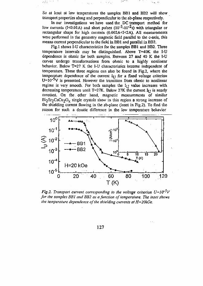
So at least at low temperatures the samples BBl and BB2 will showtransport properties along and perpendicular to the ab-plane respectively.
In our investigations we have used the DC transport method forlow currents (KO.OIA) and short pulses (10"^-10"^s) with triangular orrectangular shape for high currents (0.002A<K2A). All measurementswere performed in the geometry magnetic field parallel to the c-axis, thismeans current perpendicular to the field in BBl and parallel in BB2.
Fig.l shows I-U characteristics for the samples BBl and BB2. Threetemperature intervals may be distinguished. Above T=40K the I-Udependence is ohmic for both samples. Between 27 and 40 K the I-Ucurves undergo transformations from ohmic to a highly nonlinearbehavior. Below T=27 K the I-U characteristics become independent oftemperature. These three regions can also be found in Fig.2, where thetemperature dependence of the current IJJ for a fixed voltage criterionU=10'^V is presented. However the transition from ohmic to nonlinearregime is very smooth. For both samples the ITJ value increases withdecreasing temperature until T=27K. Below 27K the current ITJ is nearlyconstant. On the other hand, magnetic measurements of similarBi2Sr2CaCu2Ox single crystals show in this region a strong increase ofthe shielding current flowing in the ab-plane (inset in Fig.2). To find thereason for such a drastic difference in the low temperature behavior
0 20 40 60 80T(K)
100
Fig.2. Transport current corresponding to the voltage criterion U=1for the samples BBl and BB2 as a function of temperature. The inset showsthe temperature dependence of the shielding currents atH=20kOe.
127

between transport and shielding currents, we have compared the I-Ucharacteristics for both methods. Magnetization measurements [2] give asmooth powerlike dependence U~In with high values of n larger than 5.Transport I-U curves have a steplike fine structure (Fig.3). As shown in theinset of Fig.3 the voltage response in the region of the steps is not
10'
'10
10
-5
-6
T=21.8K IH=20 kOe J,
* - * 3 0
J A1.0 1.5 2.0 2.5
t(rns)
*
0.10(A)
0.15 0.20
Fig.3. Current-voltage characteristics for the sample BB2 obtained fromrectangular current pulses. The inset shows the shape of the voltage signalfor current pulse with 1=0.144A.
constant during the rectangular current pulse. The arising voltage jumps maybe explained by thermal instabilities. As shown in Ref.3 the thermalequilibrium state for high currents becomes unstable in the region where thederivative dR/dT has a sufficiently large value. Thermal instabilities can leadnot only to voltage jumps but also to periodical voltage oscillations as wasobserved in Y E ^ C ^ O y thin films [3]. Another reason for steplike finestructure might be a mechanism proposed by A.Gurevich [4]. This modelpredicts a fragmentation of magnetic flux in anisotropic superconductors withhighly nonlinear I-U dependence.
Work was supported by the Russian Foundation of Fundamental Researsh(N93-02-14768) and Scientific Council on HTSC (Russia) (Project 93173).
1. A. A. Bush et al., Superconductivity: Phys. Sci. Tech. 4 697 (1991).2. A. A. Zhukov, H. Kupfcr et al., Physica C 219,99 (1994).3. V. I. Gavrilenko ct al., Fiz. Pis'ma Zh. Tckh. 15, 83 (1989).4. A. Gurevich, Phys. Rev. Lclt. 65, 3197 (1990)
128

UA9600460

FORMATION MECHANISM OF THE (Bi,Pb)-Sr-Ca-Cu-O SYSTEM 2223 PHASEM.T. Malachevsky and D.A. Esparza - Centro Atomico Barilochc, Comision Nacional de Energia Atomica. 8400 San'
Carlos de Bariloche. Argentina. <'r
Isothermal treatments were used to investigate the transformation mechanism from 2212 to 2223 phase on the(Bi,Pb)-Sr-Ca-Cu-0 system. Silver was added in 10 wt% to observe modifications in the reaction. With the aid ofRietveld refinement, the fractional conversion of 2223 phase with time was calculated. Silver addition was observed toslow down the formation of the 2212 phase, and hence of the 2223 phase, and stabilized the PbCa2O4 phase. SEManalysis showed that the 110 K phase grew by deposition of a viscous liquid in layers over the platelets. We assignedthis mechanism to the coherent superficial nucleation of 2223 phase on 2212 plates, the rate of formation beingcontrolled by nuclei growth, that is by the velocity of migration of the liquid.INTRODUCTION
To analyze the kinetics of reaction of the 2223 phase, a non-isothermal method would hardly detect the onset of thetransformation from 2212 to 2223 as the whole range of formation-decomposition temperatures is very narrow. Inorder to get information about the 2223 phase evolution, an isothermal method should be employed. The aim of ourwork was to establish the transformation process from 2212 phase to 2223 phase as function of time, starting from amixture of oxides (with and without silver addition) submitted to isothermal anneals of different duration.EXPERIMENTAL PROCEDURE
Precursors were prepared by a citrate route [1], with nominal stoichiometry Bil.6Pb0.4Sr2Ca2Cu3Ox (BSCCO),plus 10 wt% silver (in metallic form) for the doped case (BSCCO/Ag). Neither 2212 nor 2223 phases were detected byx-ray diffraction analysis on the powders. Samples were annealed for different periods of time in an atmosphere ofnitrogen with 7% oxygen at 2223 phase formation promoting temperatures (840 °C for BSCCO and 825 °C forBSCCO/Ag). Intermediate grindings were performed after anneals of more than 50 hours, x-ray diffraction analyses ,K
were performed after each heat treatment, using CuKa radiation in 0.05° - 5 sed steps; - . , . . .RESULTS AND DISCUSSION
In a multiphase compound, if the x-ray diffraction peaks of its components do not interfere, a linear relation can be, Jobtained between the intensity ratio of the peaks of any two compounds in the mixture and their weight fraction ratjo /

|2], For our study we selected the (002) peaks of the 2212 and 2223 phases as their corresponding Bragg reflectionsare well differentiated in a mixture of both. The weight fractions of each phase were obtained from a quantitativeanalysis performed using Rietveld refinement on selected samples [3]. The results show that the quantity of 2223phase increases as the 2212 phase decreases. This is a clear indication that 2212 phase is the precursor for theformation of 2223. Once the proportionality constant is obtained for each precursor, the law followed by the fractional
Figure 1: Evolution of the fractional conversion of the 2223 phase with the annealing time. The curves result fromfitting the experimental data with an exponential law.
conversion a in each case can be easily derived from the relative intensity of the (002) peaks. Then the fractionalconversion of the 2223 phase as a function of annealing time for BSCCO and BSCCO-Ag precursors can be calculated(figure I). The experimental data were fitted to an exponential law. this approximation being good for the undopcdsamples but not for the silver-doped ones. The latter suffer an abrupt transformation after an incubation time of 20hours. X-ray analysis indicated that silver slows down the formation of 2212 phase thus retarding the appearance of

2223 phase. There exists a linear dependence of the transformation process, represented by the function g(a). withlime that makes possible to find by trial and error the function that best fits the experimental data ot(t). The mostsuitable model would be the one whose g(a) best fits a straight line when plotted as function of the annealing time.The analytical form of g(a) has been established for several models of solid state reaction mechanisms, satisfying therelation |4|:
g{a) = k(T)t or g(a) ~ - I n ( l - a ) = k(T)tr (Avrami-Yerofcev-Koglomorov relation) (1)
where k(T) is only dependent on temperature and the Avrami factor r depends on the shape of the product domains,the rate of nucleation and the type of subsequent growth of the nuclei. Four mechanisms were found to satisfy theserequirements for both precursors (figure 2 (a) and (b)). The Fl model considers the random formation of one nucleusin each particle and its subsequent growth. Taking into account that it has an Avrami factor equal to 1. this modelindicates a diffusion-controlled growth for plate-like particles, starting from instantaneous nucleation. The D2, D3 andD4 mechanisms correspond to a shrinking core model in 2 (D2) or 3 (D3 and D4) dimensions. These models assumethat when diffusion starts, a thin layer of product is already distributed coherently and propagates to the center of theparticle. In our case, for the D2 model, we have to assume that 2212 platelets have cylindrical symmetry, and arerapidly covered by a layer oflllTi that grows leaving the 2212 phase in the interior. Both D3 and D4 models assume aspherical shape for the 2212 phase with isotropical diffusion, which do not fit the real shape of the grains of thesematerials. In order to establish which model fits better the real process, samples were examined by SEM. On somegrains, a layered growth can be observed as if a liquid phase has been deposited on the plates. At increasing annealingtime, the quantity of these grains increases. For the silver-doped samples annealed for 10 hours, no grains with thesecharacteristics were found and very few can be observed for 20-hour annealed samples. These two specimens have no2223 phase as detected by x-ray diffraction. After complete transformation is achieved (150 hours annealing) allgrains present this layered morphology. We can conclude that this is the way in which the 2223 phase grows. It isevident from this observation that the mechanism of formation of the 2223 phase is better represented by the Flmodel, as the growing is not to the interior of the plates. According to this mechanism, the 2223 phase nucleatescoherently on each 2212 plate and grows by deposition of a viscous liquid in layers over the platelets. The growth rateis limited by the migration of this liquid phase. The velocity of migration must be connected with the velocities of

diffusion of Ca and Cu toward the liquid, as this phase must be rich in these elements in order to transform the 2212phase to 2223 phase.
co
(a). ., <•» / * !
D3D4
u.o \
0 -JO !00
.—•-1
Figure 2: g(a) vs. annealing time plots for the four bets fitting models for (a) BSCCO and (b) BSCCO/Ag (the delay inthe formation of the 2223 phase is taken into account by reducing the effeclive annealing time in 20 hours).
REFERENCES|1] M.T.Malachevsky. P.L.Villa and L.Gherardi. Appl. Supercond. 2. 35 (1994).[21 H.P.Klug and L.E.Alexander. X-Ray Diffraction Procedures for Polycrystalline and Amorphous Materials - Wiley-New York (1975).[3] R.J.Hill and C.J.Howard. J.Appl.Cryst. 20, 467 (1987).[4] J.Sestak. V.Satava and W.W.Wendlandt, Termochim. Acta 7. 333 (1973).

UA9600461

THE LOCATION OF TWO-DIMENSIONALSUPERCONDUCTING LAYERS IN YBa2Cu3O7
P.N.Mikheenko, V.A.Voloshin, V.V.Babenko, V.G.Boot'ko,I.M.Reznik, Ya.I.YuzhelevskiiA.Galkin Donetsk Physico-Technical Institute of the National Academy ofSciences of Ukraine, 340114, Donetsk, UKRAINE
At present there are many proofs of the two-dimensional nature ofsuperconductivity of HTSC compounds [1-7]. The aim of this paper is toestimate the thickness of the superconducting layer and to compare it with thedata, followed the obtained electron density maps.The thickness of the region where superconductive current in YBa2Cu307
flows can be found on the basis of experiments on registration of the topologicaltransition by Berezinskii-Kosterlitz-Thouless. However, some assumptionsmust be previously introduced.
It is known that at optimum doping by oxygen the every elementary unit ofYBa2Cu307 contains 0,5 holes [8 ]. Let all of them are paired. Then the
two-dimensional density of superconducting charge carriers n2D must beequal to 0,5I ab, where a and b are the lattice parameters of compound inai-plane. By numerical solving of the well-known equation for the temperatureof the topological transition TKT (see e.g. [9-11 ]):
™ _ h 2 n2D (TKT) ._- , nT ( 1 )
where m is the mass of paired charge carriers and the temperature dependencen2D(T) is presented in the form of dirty limit [9 ]
= -2D(0) ^ th ^ (2)
with the standard tabulated temperature dependence of the energy gap of thesuperconductor A (T) we obtain the difference between Tco and TKT equalto ~ 2K. This contradicts to the available experimental data, obtained on the
133

single YBa2Cu307 layers, Y/Pr superlattices and textured films, where this
difference equals to tens of K [2,6,7,12 ].
To avoid this contradiction one must assume that the thickness of a layer drestricts the mean free path of charge carriers /. Roughly speaking one canpresume that in the limit of a very thin film d identically equals I. In this casethe electron density is renormalized [9 ] down to a lower value:
>ab
where £a^ is the coherence length in the ab-plane of a compound (£a£ « 16
Angstrom [14-16]). Considering this renormalization as a basis for maximumvalues of the difference between Tco and TKT, obtained in the already citedexperimental works we find [17,18 J the thickness of a single superconductinglayer of YBa2Cu307 must be equal to 0,2-0,85 Angstrom.
In the present paper the maps of distribution of the electron density in differentplanes of an elementary cell of YBa2Cu307 are analyzed. Its structure is
represented in Fig. 1. The theoretical bases ofthe electron density map calculations aregiven in the previous papers (see [19] andreferences therein).
Fig.l.
The structure of YBa2Cu307. Dashedplanes represent the cross sections forelectron density charts. The plane restrictedby oxygen ions corresponds to Fig.2 . Theplane normal to this plane corresponds to
134

Fig.2
As is seen from Fig.2 CuO2-planes are well isolated one from another. Betweenthem the only relatively thin layer of the low collective electron density (14 eon the unit) is placed. The thickness of this layer is 0,48 Angstrom. If topresume that supercurrent flow is localized in this narrow region, the possibletwo-dimensional nature of superconductivity in HTSC compounds becomesmore understandable.
In Fig.3 ED-distribution in the plane, located between corrugated CuO2-planes is shown. It should be emphasized that in this plane only the lines withlocal ED of 1 e continuously join all parts of the elementary cell.
\
Fig.3
135

These lines form very thin "capillaries" of the thickness = 0,1 Angstrom.They are placed on the ideally flat surface in the edges of the cell, exactlybetween corrugated planes. In the center of the cell these lines brace the regionof increased electron density around the yttrium ion. If we assume that
supercurrent flow is associated with these "capillaries", anisotropy ofsuperconducting parameters in this plane is obvious. To emphasize the smallthickness of "capillaries" we show in Fig.4 and Fig.5 the maps of the electrondensity for the planes which are parallel to but placed 0.117 and 0.235Angstrom upper the plane represented in Fig.3. The evolution of the electrondensity strictly tells in favior of the existense of a thin layer which can definethe place for the movement of paired holes in this compound.
Fig.4 Fig.5
136

Table 1.
The parameters
Y
Ba
Cu1
Cu2
0 4
03
02
01
of a cell of YBa2Cu307
X
0,0000
0,0000
0,5000
0,5000
0,5000
0,5000
0,0000
0,000
used for ED calculations.
y
0,0000 -
0,0000
0,5000
0,5000
0,5000
0,0000
0,5000
0,5000
z
0,0000
0,3147
0,5000
0,1441
0,3407
0,1210
0,1240
0,5000
1. Kim / . , H.Lee, J.Chung, H.J.Shin and H.J.Lee. Phys.Rev. B 43, 2962(1991).
2. RasoltM., T.Edis andZ.Tezanovic, Phys.Rev.Lett. 66, 2927(1991)
3. Fisher K.M., Physica C 193, 401 (1992).
4. Artemenko S.N. and Yu.l.Latyshev. Modern Phys. Lett. B 6, 367(1992).5. Paracchini C. and L.Romano, Physica C 207, 143 (1993).6. Mikheenko P.N., Yu.A.Genenko, Yu.V.Medvedev, A.I.Isoskin and
I.N.Chukanova. Physica C 212, 332 (1993).7. Mikheenko P.N. and LS.Abaliosheva, Physica C 214, 393 (1993).8. Sukharevskii B.Ya., I.V.Zhikharev, S.I.Khohlova, G.E.Shatalova,
A.Ya.Duka, O.E.Tsybulskii and P.N.Mikheenko. Physica C 194, 373(1992).
9. Ivanchenko YuM. and Yu.V.Medvedev, Preprint DonPTl 84-4, Donetsk',Ukraine, 1984.
10. Ivanchenko Yu.M. and Yu.V.Medvedev and Belogolovskii. PreprintDonPTl 84-5, Donetsk, Ukraine, 1984.
137

/ / . KadinAM., Epstein and AM.Goldman, Phys.Rev. B 27, 6691 (1983).12. Norton D.P. and D.H.Lowndes, Phys.Rev. B 48, 6460 (1993).13. CrabtreeG. V., W.K.Kwok, U. Welp, R.Burriel, H.Claus, K.G. van der Voort
and J.Z.Liu. J.Magn.Magn.Materl6&.71, 547 (1988).14. Welp U., W.K.Kwok, G.V.Crabtree, K.G. van der Voort and J.Z.Liu. Phys.
Rev.Lett. 62, 1908 (1989).15. Kadowaki K. et al. Physica B 155, 136 (1989).16. FranseJ.J., J.N.Li and K.Kadowaki In:Proc. of the European Conference
on High-Tc Thin Films and Single Crystals, Ustron, Poland, 1989, p.72.
17. Mikheenko P.N. and I.S.Abaliosheva In: IV International Conference onMaterials and Mechanisms of Superconductivity High-TemperatureSuperconductors (Grenoble, France, 5-9 July 1994); Abstracts, Grenoble,1994, p.299.
18. Mikheenko P.N., V.A.Voloshin and I.S.Abaliosheva In: IV InternationalConference on Materials and Mechanisms of SuperconductivityHigh-Temperature Superconductors (Grenoble, France, 5-9 July 1994);Abstracts, Grenoble, 1994, p.298.
19. Voloshin V.A., V.V.Babenko, V.G.Boot'ko, I.M.Reznik andYa.I.Yuzhelevskii, Low Temp. Phys., 20(6), 477(1994).
20. Yokoya T, T.Takahashi, T.Mochiku, Kadawaki K. In: IV InternationalConference on Materials and Mechanisms of SuperconductivityHigh-Temperature Superconductors (Grenoble, France, 5-9 July 1994);Abstracts, Grenoble,. 1994, p.48.
138

UA9600462

LOCALIZED STATES AND SUPERCONDUCTIVITYIN BiPbSrCaCuO FILMS I
V.D.Okuneva, N.N.Pafomova, B.I.Perekrestova, I.Iguchi5 ,V.M.Svistunova
aA.A.Galkin Physico-Technical Institute of National Academy of Sciences,Donetsk 340114, Ukraine;Institute of Materials Science, University of Tsukuba, Tsukuba, Ibaraki 305,
Japan.
The influence of the metal-insulator transition (MIT) on the superconductivestate has been studied for the series of BiPbSrCaCuO films produced by themethod of DC gas discharge sputtering. We have found all the manifestationsof the superconductivity in the dielectric films as well as the appearance of"return" regions in thep (T) curves for some of them are caused exclusively bythe presence of unhomogeneities.
The present report deals with the studies on the influence of metal-insulatortransition (MIT) on the appearance of a superconductivity in BiPbSrCaCuOfilms.
The films under investigation have been produced by the technological processdescribed in [ 1 ]. There was possible to obtain the films with large variation ofproperties depending on the parameters of film growth and the subsequentthermal treatment. The films featuring the metallic mechanism of conductivity
(/? =p~i (dp /dT) > 0) with the specific resistancepc< 5- 10"3 Ohm cm
demonstrate the single-step transition with T c=l 10 K orTc=70-80K as well
as double-step one with Tc, = 110 K and Tc2 = 80 K. Where pc > 5- 10~3
Ohm • cm the Tc as a rule is below 80 K.
The sign of/3 is altered at 1.5 10 < pc< 2-10 Ohm-cm and the
behavior of p (T) curve changes to that of activation type. If the p is
increased above 2 • 10'2 Ohm • cm the T is rapidly decreased. For this case the
"return" region can appear in the p (T) curves (see fig.l, curves 1 and 2) atthe dielectric side of the MIT. For the case of the metallic conductivity the
139

I
100 200 300 IKFig.l "Return" (1 and 2) and "tail" (3 and 4) regions on the r(T) curves,
1 - the film on SrTiO , 2 - 4 - the substrate of AI2O3. On the insert - the
curve 2 replotted in the coordinates of lg(p/p300) - 10 /T.
formation of "tail" at the low-temperature region of p (T) curve (see curves
3,4 in fig.l) is possible.
Considering the mechanism of MIT for any material one have to study thep (T) dependence at the limit of T-»0 [2 ]. In our case this is impossible due tothe presence of superconducting transition.The simpler is to study the electricconductivity in the dielectric region suficiently far from the MIT. If the p ishigh enough, its thermal dependence for both the amorphous or polycrystallinefilms corresponds to the Mott law
140

For the amorphous-crystalline films with the granular structure this depend-ence is following:
[(Ti/T)1*] (2)
For the superconductive films the proof that the structure is mainly of granularnature is undirect. As is shown, the most significant changes in theconcentration of holes in the grains occur at the very beginning of theirformation when the size of metallic grains is small. With an increase in theirsize and quantity the concentration of holes become saturated. As a directresult, there is no dependence of Tc on the electric conductivity, when the lateris varied over one order of magnitude. The variation of conductivity is due tothe change of volume of the metallic phase while the concentration of holes inthe grains remains constant. Obviously, the Tc should be independent on theconductivity in this case. The dependence of p on the concentration of metallicphase Cm is shown in fig.2.
If the Cm exceeds a definite threshold, the electric conductivity is defined bythe power law:
(Cm)~(< (3)
0 H2 04- 06
Fig.2
Correlation between the specificresistance r and the concentration ofmetallic phase C.
141

As is determined by the analysis of experimental data (see fig.2), the most
certain value for C^[t is 0.20±0.01. The corresponding value of pcnt is
2-10 Ohm-cm. The value of t in (3) is l±0,05 what is obviouslycorresponding to the two-dimensional case. As is shown, the MIT in the filmsunder investigation belongs to the Anderson type. Here according to the Mottconcept on the existence of a minimal metallic conductivity,
<7min = ^ r e 2 /4zha ( B/Vo) c2
rit (4)
Here B = 2 zl is a band width, z is a coordination number,V is a randompotential and I is an overlapping integral,
I = f <E>*( r - R n ) H O ( r - R n + l ) d3x, where H is hamiltonian and
<!> (r - R) are the wavefunctions of the localized states. We have found theestimated concentration of holes in our films corresponding to the MIT. Forz = 6, Anderson localization criteterion of (V o /B) c r j t = 2 [2 ] and crmjn=
= 50 Ohm"1-cm"1 we have found that the distance between the potentialminima is a = 12 A. Considering that the distance between the CuO2 planes islesser then 12 A, the value of z = 6 is obviously better then 4. Hence, the statesare localized if there are 3.2 holes for 100 atoms of Cu. If the concentration ofholes exceeds this figure, the metallic conductivity appears. Because thesuperconductivity in high-Tc compounds is observed if the concentration ofholes is no less than 0.05-0.07 per atom of Cu [3 ], this is obviously the statewith metallic conductivity. The appearance of superconductivity at thedielectric side of MIT in our films is almost due to the existence ofunhomogeneities. Here there are the simple explanations for some complexdependencies. For example, the existence of the "return" regions in p (T)curves for some films (see fig.l) could be explained by the presence of longthin paths with the metallic conductivity surrounded by the dielectric medium.For such a topology the mean concentration of holes(over the whole samplevolume) could have the value typical for the mean concentration of the surfacestates in dielectric. Hence, the free carriers from these metallic filaments couldbe trapped in the surface states of the surrounding dielectric and the filmresistance could increase with a decrease in temperature. Here in the certaintemperature range depending on the specific energy distribution of the surface
142
states the drop of resistance is possible due to the superconductive interaction.On the inset in fig.l there is the p (T) curve for a sample of such typecharacterized by the curve 2 in fig. 1 replotted in the coordinates of lncr - 1 /T.The activation energy for T = 150-250 K is the same than that forT= 30-50 K and has a value of 3 ; 10" eV. The surface states with suchenergy could be the trapping centers only for the low (30-50K) temperaturesbut being unable to play the same role at T= 150-250K, these statesnevertheless could impede the free charge carriers.
This work is supported in part by the State Commitee for Science andTechnology of Ukraine (grant N 618). Also the authors are very grateful to theJapan Society for promotion of Science for the support in organization of theSymposium. ; •
/. V.D.Okunev, N.N.Pafomov, B.I.Perekrestov, V.M.Svistunov., JTP, Pis'ma,20 r1994), 10, pp. 60-65. . ,
2. N.F.Mott, E.A.Davis, Electron Processes in noncrystalline materials,2ed., Clarendon press. Oxford 1979.
3. M.R.Presland, J.L.Tallon et. al, PhysicaC 176 (1991), pp.95-105.,. ..
143

UA9600463
THE MICRODOPING INFLUENCE ON THESTRUCTURE AND PROPERTIES OF HIGH-TcYBa2Cu3-xMxOy SUPERCONDUC TORS.
V.P.Pashchenkoa, R.M.Poritskib , V.B.Tuytuynnikb ,O.P.Cherenkova, E.P.Strekalovab.aA.Galkin Donetsk Physico-Technical Institute of Ukrainian Academy ofSciences, Donetsk,340114, the Ukraine;bResearch Institute "Reaktivelectron", 96,Bakinskih Komissarov str.,Donetsk, Ukraine
A determination of the role of admixture ions differed by charge states,covalences and magnetic properties.
"Using X-ray, magnetic, microscopic, hydrostatic and Moessbauermethods the ceramic high temperature superconductorsYBa2Cu3_xMxOy microdoped (0.0 < x < 0,1) by metal oxides with different
valences (MnO, Fe2O3 , ZrO2 , Nb2O5 ) were investigated. A choice of suchsmall quantities of dopants was due to a number of factors, amongst of whichan inevitability of presence of small impurities , a greater possibility of smallquantities solubility into main phase and superconducting preservation shouldbe marked.
According to X-ray diffraction data, all the investigated samples areidentified as single-phase ones. However, there is no basis to consider themas single-phase ones, because the small addition quantities can beinhomogeneously distributed in the main ortho rhombic phase or even cansegregate forming into intercrystalline zones, the more disordered ones ormicrophases.The doping can lead to a change of oxygen content andsuperconductive transition temperature [1 ].
A nonmonotonous character of a number of physical parameters dependingupon additions content testifies to the complicated physical and chemicalnature of their influence on the structure and properties of HTSC.
The investigations of MnO and Fe2O3 influence revealed the oxygen contentis changing weakly, especially under Mn doping, because of valence change of
144

UA9600464

copper {2 j and manganese [3 ]. The analysis of temperature dependences ofX in comparison with data on oxygen content and its distribution along aand b directions of single-phase samples rhombic structure allows to drawa conclusion that Mn is mainly in the two-valent and partly in three- andfour-valent [4 ] states forming a superposition of multy-valent states [5]and replacing the copper cations in the Cu(l) and Cu(2) posi tions respectively.Fe is in the three- and two-valent states. So, the oxygen and anionicvacansies in ab plane redistribute changing a degree of rhombic distortion.
The sufficient changes of samples density and porosity testify not only toMn and Fe influence on real structure , but on the crystallite-porous onetoo. The extremes at x = 0.02 - 0.04 are observed in the concentrationcurves of a number of parameters ( Tc,
cTc,V la tce l l ,p ets.).
The analysis of Fe cations influence, in comparison with data includingMossbauer ones on the solubility and positions of Fe ions [6,7 ], showed theoxygen content decrease at# increase is due to the changes of Fe and Cuvalencies mainly under anionic vacances formation violating a superexchangeinteraction and anisotropy in the Cu-O-Cu chain and decreasing thetemperature of the transition beginning into superconducting state.
The investigations of ZrO2 and Nb2O5 influence showed the oxygen content,porosity and a volume of lattice cell are changing more sufficiently under thismetaloxide microdoping with higher charge state of cations. That is why, theextremes of parameters at x = 0.02 - 0.04 were discovered too. It is in part due,in our opinion, to a limited solubility of Zr and Nb in the main phase and theirlocalization in intercrystallite zones and a formation of structural-chemical inhomogeneities.
Ther are remarkable extremes also observed at x = 0.02-0.04 atmicrodoping of not only HTSC, but other metal-oxides too.
That is why a conclusion is drawn that such an influence of concentrationhas more general physical nature.This is due not only to a certain real andcrystalline-chemical structure formation but isotopic oxygen content, O(0.04%), too. Thus, the microdoping influence by cations with differentvalences on the structure and properties of HTSC was determined in thiswork, using complex methods. A complicated character of microdopings
145

influence and extremum presence in concentration curves of a number ofmicroadditions were shown, the assumptions about possible causes of aphysical nature of these extremums were made. An elucidation of these causesdemands for the further investigations.
1. V.P.Pashchenko, V.T.Pitsyuga, V.S.Abramov. In:Fiziko-himia itehnoLvysokotemp. sverhprov. mater. M., Nauka. I9S8, p. 152- 155.
2. M.A.Poray-Koshits. Izv.DANSSSR 305, F4, 906 (1989).3. G.N.Kuzmitchova, E.P.Khlystov. Izv.AN SSSR. Neorgan.mater.-K 199O.-c26J6.- p. 1264-1266.4. Muralidharan P. Umadevi, A.D.Damodaran. Jap. J.Appl.Phys.Pt. 1.-199L-. 30,F2.-p.280-281.5. V.P.Pashchenko, Z.ASamoilenko and all, Conference "Material.VTSP",
Kharkov, the Ukraine, April 5-9, 19931 3,33.6. I.V.Boidachenko, A.O.Komarov. Fiziko-himia i tehnol. vysokotemp.
sverhprov. mater. - M., Nauka.- 1988.- p. 102-103.7. L.Nunes, R.D.Rogers, G.W.Grabtec, U.Welp, K.Vandervoort, A.Umezawa,
Y.Fang. Phys.Rev. B.-1991.-44, F9.- p.4526-4531.
146

HTSC CERAMIC CURRENT-TRANSPORT DEVICES
B.LPerekrestov3, A.V.Vasilenkoa, J.Leszczynskib
aA.A.Galkin Physico-Technical Institute of National Ukrainian Academy ofSciences,bInstitute of Principles of Electrical Power Engineering 1-12, TechnicalUniversity of Lodz, 18/22, B.Stefanowskiego str., 90-924 lodz, Poland
The technology for production of the current-transport devices of Bi-2223ceramic with the Jc =1.2-3.1 kA/cm and Ic > 250 A have been developed andapplied to produce the current terminals for the superconductive magnetsystems. The heat con duction of these devices was found to be 6 times lower thanthat of the convention copper ones at T=* 77 Kin helium atmosphere what makesthem good thermal decouplers.
We have developed and successfully applied the methods of fabrication of theHigh-Tc ceramic devices providing the critical currents of several hundredAmps [1 ]. These devices could be made of various sizes and cross-sections andcould be used as the current terminals for the superconductive magnetsystems operating at the liquid helium temperature. The heat released insidethe helium bath depends on the dissipation in these terminals and their heatconductance. The dissipation is canceled using the high-Tc superconductor asa material of current terminals but the heat conduction remains. At the lowtemperatures this heat flux is quite low [2 ] but it should be considerable atT=77 K.
The present study is intended to determine the current-transport propertiesand heat conduction of prototype current terminal in the gas-phase heliumenvironment at T = 77K in comparison with the conventional copper currentterminal. The HTS ceramic devices were of tubular shape having the lengthsof 150-200mm and wall thickness of 0.3-0.4mm. The material was the Bi-2223ceramic. The powder of the initial compound together with 5-10% of plastifierwas subjected to hydroextrusion to determine the geometry. After the removalof plastifier the samples were annealed by two steps with the additionhydrostatic pressing at P = 5-6 kbar.
The electrical measurements were performed using the four- probe method.
147

The critical current was taken at E = 1 /uV/cm. The typical R (T) curve for thecurrent terminal with Tc = 110 K is shown in fig. I (curve 3). The narrowtransition width is indicative of a good quality of grain interfaces anduniformity of current-transporting cluster. The typical critical current densitywas J c= 1.2-3.1 kA/cm2. The JC(H) dependence of this samples is similarthan that of the flat ones [3 ]. There is a sharp drop of J at the low fields but atH = 1 kOe the JC(H) has a plateau. The small abnormal hysteresis of JC(H) isspecific for the granular structures [4 ] with the good quality of grain interfaces.
The heat conduction w of these samples as well as that of copper ones of thesame geometry was measured using the single-axis heat flux induced by thelocal heater [2 ]. The gradient of temperature along the sample was monitoredby the resistive sensors made of fine copper wire. The power of the local heaterwas kept the same for both the ceramic and copper samples. Results ofmeasurements of dT = Tj-T2 « 1 /w are shown in fig. 1, where Tj is thetemperature near the heater and T2 is the temperature in a distance about 6mm from heater. The heat conduction for the ceramic devices have been
Fig.l. Dependencies of T(T) for ceramic current terminal (1) and coppersample (2) and the R (T) curve (3) for the HTS ceramic.
148
determined to be lower that that of copper ones by the factor of 6. So, even atT = 77 K the ceramic inserts could serve as the good thermal decouplerssignificantly reducing the heat flux from outside to the helium bath.
Acknowledgments. The authors are grateful to Japan Society for Promotion ofScience for financial support of the Symposium.The work was also supportedby the State Committee on Science and Technology of The Ukraine (projectN 0.901.04/057-94).
7. Perekrestov B.I., Tarenkov V.Yu., Dyachenko A.I. et al. FTVD, 1993, .3;P. 131-135. .f
2. Kirichenko Yu.A., Rusanov K.V., T'urina E.G. SPOT, 1990, 3,.P. 1385-1409.
3. Svistunov V.M., EfyachenkoA.1., Tarenkov V. Yu., Perekrestov B.I. FTVD,1992, 2, P.5-15.
4. Svistunov V.M., UyachenkoA.L, Tarenkov V. Yu.PhysicaC. 1991,185-189,P.2429-2430.
149
HIGH PRESSURE EFFECT ON STRUCTURE ANDPROPERTIES OF MeBa2Cii3O7-<5 (Me =La.Nd.Gd,Sm,Eu)HTSC CERAMICS
, 9 UA9600465T.A.Prikhna1, V.S.Melnikov% V.E.Moshcil\ V.V.KovylaeV,V.F.Solovyov , P.A.Nagorny1 V.N.Bakul Institute forSuperhard Materials, 2 Avtozavodskaya Str., 254153,Kiev, Ukraine; 2Institute of Geochemistry, Mineralogy and Oreformation,institute of Materials Science Problems, 4Institute of Metal Physics, all of theUkrainian National Academy of Sciences
The influence of high pressures (2-6 GPa) and temperatures (900~1200°C) hasbeen studied on the structure, phase composition, superconductive andmechanical properties o/MeBa^CugO^ (Me-La,Nd,Gd,Sm,Eu).
The high pressure - high temperature (HP-HT) conditions have been createdusing a recessed-anvil-type high pressure apparatus, the samples have beeninsulated from a graphite heater by the use of zirconia [ 1 ]. The accuracy of thepressure and temperature measurements were ± 0,15 GPa and ± 20°C, whilethe rates of sample heating and cooling made about 1000 and 400 °C/min,respectively. The electrical resistance of the samples have been determinedusing the magnetical measurements. An AflIT-1 difractometer and a JeolSuperprobe-733 X-ray microanalyzer (Japan) were employed to evaluate thesample phase composition and crystallographic parameters, to do thequantitative analyses. A MXT 70 Matsuzava microhardness tester has beenused to measure Vicker's microhardness.
X-ray examination show that the unit cell parameters of as-treated at thegiven temperature 123 phases are strongly pressure-dependent. In generalcase (for P=2 and 5 GPA) (Fig), the decrease of the c-parameter with thetemperature increase from 900 up to 1200°C is observed. But the mode ofc-parameter variations for different 123 compounds differ sharply. At P== 2 GPa, the c-parameter decreases with the temperature increasing is mostdistinct. The Gdl23 and Eul23 demonstrate the maximum c-parameterdecreases at 1200°C that makes 0,15 and 0,08 A, respectively. This is
150
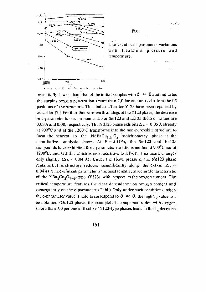
Fig.
The c-unit cell parameter variationswith treatment pressure andtemperature.
• T , ' C• - Nd O - (3d A - S I T I ? - Eu a - l a
essentially lower than that of the initial samples with d ~ 0 and indicatesthe surplus oxygen penetration (more than 7,0 for one unit cell) into the 05positions of the structure. The similar effect for Y123 have been reported byus earlier [2 ]. For the other rare-earth analogs of the Y123 phase, the decreasein c-parameter is less pronounced. For Sml23 and Lai23 the A c values are0,03 A and 0,00, respectively. The Ndl 23 phase exhibits A c » 0,05 A alreadyat 900°C and at the 1200°C transforms into the non-perovskite structure toform the nearest to the NdBaCuj 64OX stoichiometry phase as thequantitative analysis shows. At P = 5 GPa, the Sml23 and Eul23compounds have exhibited the c-parameter variations neither at 900°C nor at1200°C, and Gdl23, which is most sensitive to HP-HT treatment, changesonly slightly (Ac = 0,04 A). Under the above pressure, the Ndl23 phaseremains but its structure reduces insignificantly along the c-axis ( A c -0,04 A). The c-unit cell parameter is the most sensitive structural characteristicof the YBa2Cu3O7_(5-type (Y123) with respect to the oxygen content. The
critical temperature features the clear dependence on oxygen content andconsequently on the c-parameter (Tabl.) Only under such conditions, whenthe c-parameter value is hold to correspond to d ~ 0, the high Tc value canbe obtained (Gdl23 phase, for example). The supersaturation with oxygen(more than 7,0 per one unit cell) of Y123-type phases leads to the Tc decrease
151

Table
Crystallographical parameters, temperature of SC transition and Vickersmicrohardness versus of the process technological parameters
No
1
2
3
4
5
6
7
8
9
10
11
12
13
14
15
16
17
18
19
20
21
22
23
Com-pound
Nd(123)_ it _
- " -
- " -
Sm(123)
- " -— " _
Eu(123)
- " -
- " -
Gd (123)
- " -. " .
- " -
_ «
La (123)
Treatmentconditions
P,GPa
T,oC min
initial sample
2
5
6
2
5
900
900
900
1200
1200
30
30
30
10
10
initial sample
2
2
5
900
1200
1200
30
10
10
initial sample
2
2
5
900
1200
1200
30
10
10
initial sample
2
5
2
5
6
900
900
1200
1200
900
30
30
10
10
30
initial sample
2
2
900
1200
30
10
Temperatureof theSC-
transition, K
Tel
89
Tc2
81
absent
79
-
60
-
absent
absent
80
48
-
50
83
74
74
92
75
26
26
79
30
34
90
absent
35 67
absent
-
-
-
-
12
-
-
-
Vickersnicrohardness
GPa,at2-N load
1.2
5.9, 1.2
-
7.6,3.1,5.8
5.6,4.1
1.4
5.8 2.6
5.4
-
-
5.9,2.9
4.5
5.7
0.3
5.6, 3.0
-
4.3,2.2, 1.2
2.7,2.0
-
1.3
-
4.8, 2.8, 0.9
152

or absence of the superconductivity. Another factor that influences the Tc
decrease is the presence of the admixture phases in the initial material. Theadmixture phases can appear also in the HP-HT treatment process and,apparently, the higher pressures (5-6 GPa) hinder the process. The phasetransformation in Ndl23 under 2 GPa and T > 900°C may be connected withthe structure supersaturation with oxygen, but the X-ray diffractionpattern shows the high homogeneity of the product obtained (it is practicallysingle-phased). The microhardness tests show an essential increase in.microhardness of the samples after HP-HT treatment due to densification. Butin case of multiphase samples, the microhardness values of the same samplediffer greatly.
/. Prikhna T.A. elal. Superconductivity, 5, N4, P.666-672, (1992).2. Prikhna T.A. et al. Fizika i Teknika Vysokikh Davlenii, 1, Nl, P.84-88,
(1991).
153

X-RAY ELECTRON SPECTROSCOPY STUDYOF THE ELECTRON STRUCTURE OF YBa2Cu3O7-x
I.N.Shabanova, S.F.Lomaeva, N.S.Terebova,N. M. NebogatikovPhysico-Technical Institute, Ural Scientific Center, Kirov st.132,Izhevsk, 426001, Russia
UA9600466The determination of superconductivity mechanism as well as the stabilityboundaries of superconductive phases is an important problem of high-temperature superconductivity physics. The present report deals with the studiesof the electron structure changes at the superconductive transition of high-temperature superconductive compounds (HTSC) (YBa2Cu307_x^.
The method of X-Ray electron spectroscopy is most suitable to investigatethe electron structure and that of chemical bonds, because it does not derstructthe latter in the analyzed layer (20-30 A). The X-Ray electron magneticspectrometers [ 1 ] used in this work allow to obtain the spectra within thetemperature range from liquid nitrogen to 2000°C with layer by layermechanical cleaning of the sample surface in the superhigh vacuum [2 ].
The sample was cooled down to -196oC in the operating chamber of thespectrometer. The temperature of the sample surface was kept constant andmonitored during the whole experiment. The cooling agent was the liquidnitrogen. The cooled sample surface was cleaned with the diamond film toremove the adsorbed substances before recording the each-spectrum. Theinstrument resolution was (1-1,2 eV), the accuracy of X- Ray electron statespectra measurement was 0,1 eV. The intensity scattering was 5%.
YBa2Cu307_x films were deposited onto (001) Si with the barrier layer of
ZrO2. The barrier layer thickness of semicrystalline ZrO2 is 1 /im. Thedeposition time was four hours, the film thickness was 2-3 /um. The substratetemperature was 250-300°C.
The comparative study of YBa2Cu307_x sample at room temperature and that
of liquid nitrogen was carried out.
154

The spectra of inner levels of 01s, Cu3p, Ba3d,Y3d and the valence band wererecorded. The spectra of Cu3p were chosen to study the chemical state of Cuatoms because of a greater kinetic energy of electrons and hence their exit fromthe most deep surface layer in comparison with the electrons of 2p level. TheCu3p, Ba3d, Ols and valence band spectra of YBa2Cu307_x sample are
presented in Fig. 1.
The analysis of the obtained data showed that Cu atoms are in three states:with the lesser (Cul) and the greater (Cu2) number of oxygen atoms aroundthe Cu atoms and CuO with the deficit of oxygen atoms in Cu environment.The CuO state at the room temperature is expressed poorly.The electron Ba 1 state with the oxygen deficit in the environment of Ba prevails
VALEKCf Mh'D
785
Fig. 1. The X-Ray electron spectra of Cu3p, Ba3d, Ols and valence band.a) T = +30°C the surface without mechanical cleaning; b) T=+30°C thesurface after mechanical cleaning; c) T = -190°C the surface is cleanedcompletely; d) the valence band of Cu; e) the density of states 13 ].
155

in Ba spectrum than Ba2 at room temperature. This is due to the more probablelocation of oxygen vacancy in 01 oxygen position on axis from our point ofview.
The CuO state intensity due to oxygen deficit in Cu environment and that ofBa2 because of more higher number of oxygen atoms around Ba are relativelyincreased at the temperature of -196 °C. This fact can be explained supposingthe most probable path of oxygen ionsdiffusion in the YBa2Cu307_x is from
04 position in Cu-0 plane to 01 oxygen position on c-axis.
The study of valence band spectra showed a strong hybridization of Cu3d and02*p states reflecting the changes taking place in the neighboring environmentof Cu and O atoms what results in the overlapping of Cu3d and 02p electronorbitals.
/. Trapeznikov V.A., Skabanova I.N. el.al. lzv.Akad.Nauk SSSR, serfiz., 50(1986) 1677.
2. Shabanoval.N. et.al Melallofiz., 3 (1981) 102.3. Massida S., Jaejun Y.U. et al. Physics Letters A 122 (1987) 198.
156

UA9600467

CORRELATION BETWEEN THESUPERCONDUCTIVITY AND STRUCTURE OFBiPbSrCaCu FILMS.
Z.A.Samoilenko, V.D.Okunev, E.I.Pushenko, N.N.PafomoyA.Galkin Physico-Technical Institute of Ukraine National Academy ofSciences, Donetsk 340114, Ukraine
The amorphous films of different thicknesses already in the initial state werecharacterized by diffraction patterns differed by width, B, location jof halomaximum, ©, and the intensity of incoherent Compton scattering of roentggn(CrKa ) radiation (Fig. 1).From B and © values the estimation of clustersizes,m, {1 ]and interplanar distances,d, in the mesoscbpic atom groupings ofobtained films have been determined (Fig.2). One can see from Fig. 1,2 thatwith the increase of film thickness, h, the decrease of m is observed at thedecrease of average interplanar distances inside the clusters
50
0.50 h
- \ •
\
v
\• - . _
y Ns \
\\
a u 26 2i s;
Fig.l
1 3 5 ? i.HKH
Fig.2
Fig. 1 .Diffusion halo on roentgenograms of amorphous films with thickness 0.3(a), 1.1 (b), 3.3 (c) and 6.3 (d) mu.
Fig.2. Dependence of cluster sizes, m, interplanar distances, d, and intensitiesratio Inoncoh / I c o h on film thicknesses, h.
157
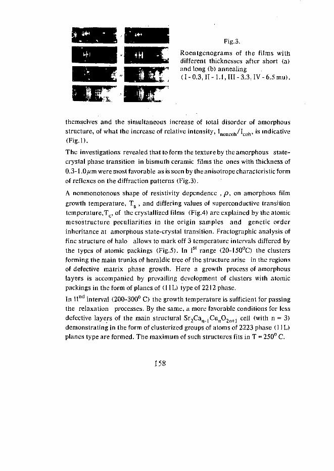
Fig.3.
Roentgenograms of the films withdifferent thicknesses after short (a)and long (b) annealing(1-0.3, II-l . l ,III-3.3,IV-6.5mu).
themselves and the simultaneous increase of total disorder of amorphousstructure, of what the increase of relative intensity, Inoncoh/ICOh>ls indicative(Fig.l).
The investigations revealed that to form the texture by the amorphous state-crystal phase transition in bismuth ceramic films the ones with thickness of0.3-1.OjHtn were most favorable as is seen by the anisotrope characteristic formof reflexes on the diffraction patterns (Fig.3).
A nonmonotonous shape of resistivity dependence , p, on amorphous filmgrowth temperature, Ts , and differing values of superconductive transitiontemperature,Tc, of the crystallized films (Fig.4) are explained by the atomicmesostructure peculiarities in the origin samples and genetic orderinheritance at amorphous state-crystal transition. Fractographic analysis offine structure of halo allows to mark off 3 temperature intervals differed bythe types of atomic packings (Fig.5). In Is1 range (20-150°C) the clustersforming the main trunks of heraldic tree of the structure arise in the regionsof defective matrix phase growth. Here a growth process of amorphouslayers is accompanied by prevailing development of clusters with atomicpackings in the form of planes of (11L) type of 2212 phase.
In II" interval (200-300° C) the growth temperature is sufficient for passingthe relaxation processes. By the same, a more favorable conditions for lessdefective layers of the main structural Sr2Can jCun02n+1 cell (with n = 3)demonstrating in the form of clusterized groups of atoms of 2223 phase (11L)planes type are formed. The maximum of such structures fits in T = 250° C.
158

•vif-
i aU. , :| " SO 160 2<Q r*
0 OT""?O0"l0b(00..
Fig.4 Fig.5Fig.4. Dependence of resistivity of amorphous (1) and crystallized (2) samples
on T .In the insert: the temperature dependence of resistance afterhigh-temperature annealing.
Fig.5. Phase composition of films in initial state depending on T .
In IIIr interval (350-450° C) a growth temperatures are sufficient not only toform undercriHeal germs of crystalline structure (clusters), but the morelarge-scale, critical ones too. In this region the change of crystallographicdirection of ordering atomic layers as a planes of 2223 phase planes of (00L)type is a distinctive feature of atomic order formation. •••
This work was supported by Ukrainian Govennent, HTSC grant N 618.
/. V.D.Okunev, Z.A.Samoilenko, E.I.Pushenko, J.F.Revenko,B.I.Perekrestov. Neorganicheskiematerialy. - RAN, 1994. - 330, P l.-p. 1-5.
159

CORRESPONDENCE OF THE Tc VALUES FORYBa2Cii3O6+<5 COMPOUNDS TO THE POSITIONS OFLABILITY BOUNDARIES FOR THE ORTHO- ANDTETRA-PHASES ON THEncuO2-<5 STATE DIAGRAM
•Ya.Sukharevskn UA9600468A.A.Galkin Physico-Technical Institute of National Academy of Sciences ofUkraine, Donetsk, Ukraine.
The present report is intended to describe the further development of problemfirst discussed in [ 1 ]. The main goal is to give a background for the twofollowing hypotheses.
1. The charge carrier concentration at the CuO2 planes in the HTS cupratescorresponds to the position of lability boundaries on the n - 6 diagram.
2. The Tc values for the HTS compounds are proportional to the charge carrier
concentration n ^ u Q at the CuO2 planes. The d is determined by the
difference in the number of electrons per formula unit for the superconductiveand dielectric phases of the given cuprate. For the compounds of YBa2Cu30x
type the dielectric analog is YBa2Cu2+Cu+06, sod = x - 6. The total number
of charge carriers (holes) is 26 = n t o t
2(5 = n + n C u + + nCuOd ,
where n = riQuQ >ricuo+ i s a n u m ^ e r °f ion-bound holes n ^ o ^ - number
of holes at the fragments of copper-oxygen chains terminated by the oxygenvacancies.
To determine the lability boundaries one have to examine the Landaupotential
0> = aoV2 + borj4 + or}6 + d£2 + ft]112 + g | 4
here rj and £ are the order parameters. The factors of a0, bo,d and f are
160

To/To 111
Fig.l.The phase diagram. 1: b2 - 3ac = 0, 2: a = 0, 2': a0 - 0.1- tetra-phase I(r] = o, | = 0), II- ortho-phase II ty * 0, £ = 0), III- tetra- phase II(77 = 0 , 1 ^ 0), IV- ortho-phase I ty * 0,£ * 0). Experimental points:• - [ 3 ] , o - [4] ,x-[5] ,A~[6] , -[7].
the linear functions on n and d. These dependencies determine the
positions of lability boundaries on the n -6 diagram. They correspond to
the experimental data for the positions of the apex of parabola 1 (see Fig.l),
the polycritical point nQ, (50 and d (n=€). The renormalized quantities a and
b , used during the analysis are the following
a = ao-fd/2g, b = bo-f2/4g.The results of analysis of the Landau potential <2> are demonstrated inFig.l. The regions I,II,III and IV correspond respectively to the tetragonalphase I , orthorhombic phase II tetragonal phase II and orthorhombic phaseII. , , ...: ^ , ... w "
To test the abovementioned hypotheses, the experimental data points takenfrom [2,3,4,6,7] are put on this phase diagram. The n values are derived
161

from the data on diamagnetic responce [2,3,4], Hall effect [5], Moessbauereffect [6 ] and Neel temperature asa function of oxygen content [7 ], assumingthat n ~ Tc and with the use of theoretical results of [8,9].
As a result, the both mentioned hypotheses are confirmed. The points obtained
assuming the Tc is proportional to n^uO together with ones representing n
(d) by the data of Hall and Moessbauer effects as well as TN (d) lay at the lineof type II phase transition (curve 2' in Fig. 1) and at the upper and lower labilityboundaries (curves 1 and 2 for the decrease and increase in <5, respectively).To obtain the additional facts that these hypotheses are true one can comparethe values of r/+ and r\_ (for the upper and lower lability boundaries)
calculated using the potential O with the experimental data on (b-a)/btaken from [3,4 ], as is shown in Fig.2.
The examined system is completely determined by the potential ofO (j]o , £o) (here (tjQ , £0) are the equilibrium values for the order
parameters, so £ means RQuQd • Fig.3 shows the theoretical values ofnCu0<5 an(* n C u + = 2(3—n— JtlCuOd together with the same quantities
derived from the Moessbauer data [6 ]. That is why, the assumption that
Tc ~ riQuo and the values of n^uQ correspond to the lability boundariesLi id
08
OS
Fig.2.
The orderparameter ?)+
(b2 - 3ac = 0) andrj- (a = 0). Solid
CL4 line - theory, thedots - experiment
02 I 3 ' 4 * -
00 08 _ 080
162
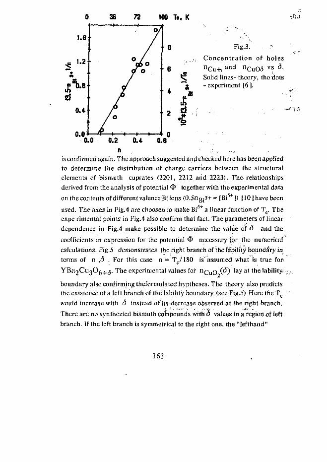
36 100 T«. K
Fig.3. -
Concentration of holesnCu+. a n d nCu0<5 v* d-Solid lines- theory, the dots- experiment [6 ].
0.0
is confirmed again. The approach suggested and checked here has been appliedto determine the distribution of charge carriers between the structuralelements of bismuth cuprates (2201, 2212 and 2223). The relationshipsderived from the analysis of potential 4> together with the experimental dataon thecontents of different valence Bi ions (O.5rigj3+ = [Bi +j) [10 J have been
used. The axes in Fig.4 are choosen to make Bi5+ a linear function of Tfi. Theexpe rimental points in Fig.4 also confirm that fact. The parameters of lineardependence in Fig.4 make possible to determine the value of d and thecoefficients in expression for the potential <£ necessary for the numericalcalculations. Fig.5 demonstrates the right branch of the lability boundary interms of n ,d . For this case n = Tc/180 is'assumed what is true for,
. The experimental values for (d) lay at the lability;.^
boundary also confirming theformulatedhyptheses. The theory also predictsthe existence of a left branch of the lability boundary (see Fig.5) Here the Tc "would increase with <5 instead of its decrease observed at the right branch.There are no synthezied bismuth compounds with 0 values in a region of leftbranch. If the left branch is symmetrical to the right one, the "lefthand"
163

n1.0
as
08
<u
02
Fig 4.
Correlation between the Tc andrig 3-J™. The dots - experimental
data for 2201. 2212 and 2223phases [10].
no 02 ae as 1.0
superconductive compounds would have <5 > 0.25. These two branches have a
cross point at 5 = 1 . The maximal Tc = 120K. It should be noted that the
dependence of Tc(<5 ) shown in Fig.5 is the same for the compounds
tJ^oi2*--"*-'6+(5 > ^"2 2 2 8+<5 ^ n " "*2 2 2 3 10+<3 *
For each compound at d = 1 the value of Tc = 120K is theoretically possible
1.3 1.4 1.5 1.8
Fig.5.
Phase diagram. Solidline is the labilityboundary forb2 - 3ac = O,the dots-experiment [10].Insert: the schematicdiagram for labilityboundaries.
164
but perhaps the limit for n in CuO2 planes is about 0.2-0.3 holes per formulaunit what corresponds tp the well-known Chu rule.
/. B. YcuSukharevskii, Low Temp. Phys., 20(2), 97, february 19942. B. YcuSukharevskii, I. V.Zhikharev, S.I. Khokhlova et al, Physica C 194*'373
(1992)3. E.Takayama-Muromachi, Y.Uchida, H.Ishii et al, Jpn. J. Appl. Phys. 26,
L1156(1987)4.1. V.Aleksandrov, A.B.Bykov, I.P.Zibrov el al, JETP left., 48, 493(1988)5. Z.Z. Wang, J.Clayhold, N.P.Onget al, Phys. Rev., B36, 7222(1987)6. I.V.Vilkova, L.A.Ivchenko, V.G. Ksenofontov et al, Hyperfine Interactions,
70, 1223(1992)7. J.M.Tranquada, A.H.Moudden, A.Y.Goldman et al Phys. Rev., B38(4),
2477(1988)8. A.A.Lushnikov, JETP, 56(1), 215(1969)9. M.M.Bogdan and A.S.Kovalev, Fiz. Nizk. Temp., 16, 1576(1990)W.Kazushige Ohbayashi, Kenji Yoshida, Masatoshi Anma et al, Jpn. J. Appl.
Phys., 31, L953(1992)
165
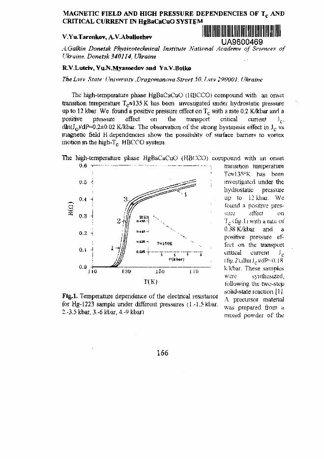
MAGNETIC FIELD AND HIGH PRESSURE DEPENDENCIES OF Tc ANDCRITICAL CURRENT IN HgBaCaCuO SYSTEM
V.Yu.Tarenkov, A.V.AballoShev UA9600469
A.Galkin Donetsk Physicotechnical Institute National Academv of Sciences ofUkraine. Donetsk 340114, Ukraine
R.V.Lutciv, Yu.N.Myasoedov and Ya.V.Boiko
TheLviv State University .Dragomanova Street tO. Lviv 290001, Ukraine
The high-temperature phase HgBaCaCuO (HBCCO) compound with an onsettransition temperature 7^135 K has been investigated under hydrostatic pressureup to 12 kbar. We found a positive pressure effect on Tc with a rate 0.2 K/kbar and apositive pressure effect on the transport critical current Jc,dln(,Jc)/dP=0.2±0.02 K/kbar. The observation of tlie stiong hysteresis effect in Jc vsmagnetic field H dependencies show the possibility of surface barriers to vortexmotion in the high-Tc HBCCO system.
The high-temperature phase HgBaCaCuO (HBCCO) compound with an onsettransition temperatureTc*135°K. has beeninvestigated under thehydrostatic pressureup to \2 kbar. Wefound a positive pres-sure effect onTc(fig.l J with a rale of0.38 K/kbar and apositive pressure ef-fect on the transportcritical current Jc
ffiti.2UHn(Jc)/dP-0.18k-'kbar. These sampleswere synthesized,following the two-stepsolid-state reaction [1).A precursor materialwas prepared from amixed powder of the
0.6
0.5
0.4 -i
0.3 -t
0.2
0.0130 150 1 VO
T(K)
Fig.1. Temperature dependence of the electrical resistancefor Hg-1223 sample under different pressures (1.-1.5 kbar,2.-3.5 kbar, 3.-6 kbar, 4.-9 kbar)
166
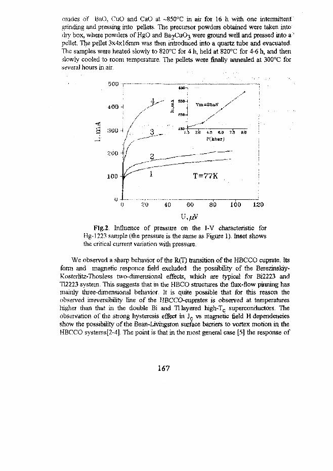
oxides of BaO. CuO and CaO at ~850°C in air for 16 h with one intermittentgrinding and pressing into pellets. The precursor powders obtained were taken intodry box, where powders of HgO and Ba?CuC>3 were ground well and pressed into a 'pellet. The pellet 3x4xl6mm was then introduced into a quartz tube and evacuated.The samples were heated slowly to 820°C for 4 h, held at 820°C for 4-6 h, and thenslowly cooled to room temperature. The pellets were finally annealed at 300°C forseveral hours in air.
500
400 -!
B 300-i
200 ->
100
Flg.2. Influence of pressure on the I-V characteristic forHg-1223 sample (the pressxire is the same as Figure 1). Inset showsthe critical current variation with pressure.
We observed a sharp behavior of the R(T) transition of the HBCCO cuprate. Itsform and magnetic responce field excluded the possibility of the Berezinskiy-Kosterlitz-Thouless two-dimensional effects, which are typical for Bi2223 andT12223 system. This suggests that in die HBCO structures the flux-flow pinning hasmainly three-dimensional behavior. It is quite possible that for this reason theobserved irreversibility line of the HBCCO-cuprates is observed at. temperatureshigher than that in the double Bi and Tl layered high-Tc superconductors. Theobservation of the strong hysteresis effect in Jc vs magnetic field H dependenciesshow the possibility of the Bean-Livingston surface barriers to vortex motion in theHBCCO systems[2-4]. The point is that in the most general case [5] the response of
167
the critical current Ic of Josephson junctions to a magnetic field H is determined bythe magnitude of the surface current Jsf induced in the granules. In the presence ofthe surface barrier for the increasing fields J s r ^ c ^ ^ lcCup)~l/Jsf-l/Hc, while fordecreasing fields Jsf~Hcl and Ic(downV-l/Hc]. That is why !c(up)«Ic(dowTV
Acknowledgments
The work was supported by the State Committee on Science and Technology ofThe Ukraine (project N 09.01.01/056-94).The authors are grateful to Japan Societyfor Promotion of Science for financial support of the Symposium find toProf. V.M.Svistunov for stimulating and heJpful discussions.
References
[lj S.N.Putilin, I.Bryntse and E.V.Antipov, Matr. Res. Bull. 26 (1991) 1299.[2] L.Burlachkov, M.Konczykowski, Y.Yeshurun and F Holtzbarg, J.Appl.Phys. 70(1991)5759.[3] M.Xu, D.K.Finnempre. G.W.Crabtree, V.M. Vinokur, K.Zhang, B.Darbowski,and D.G.Hinks: Phys. Rev. B 48 (1993) 10630.[4] N.Chikumoto, M.Konczykowski- N.Motohura. and A.P Malozemoff, Phys. Rev.Lett. 69 (1992)1260.[5] A.l.D'yachenko, Physica C 213 (1993) 167
168

Modification of YBa2Cu307^ Ceramics after PulseNeodymium Laser Irradiation
M.WLVasygk, R.V. Lutciv UA9600470HTSC Laboratory, Dep. of Physics, Lviv State University,Lviv,UA-290005Ukraine
the transport properties, surface morphology and stoichiometry ofYBa2Cu3O7.5 after neodymium laser irradiation were investigated. Lasertreatment produces a general increase of resistivity and a change in theresistivity temperature dependence type from metallic to semiconductor,ceramics surface morphology and distributions of K^Cu) and La(Ba) linesfrom X-ray microprobe analysis are more uniformly on irradiated regions ofsamples. We observed decreasing of oxygen contents, carbon and copperconcentrations on the irradiated surfaces using Auger-electron spectroscopy.
Loss the oxygen is a native process, which determins phasetransitions at treatment HTSC by different types of irradiation such aselectrons, ions and so on'[1,2]. The change of distributions of anotherceramic components also can lead to changes of samples YBa2Cu3O7.s
properties. The condition of surface ceramics before and after laserillumination is a important part of our reseaches.
The influence of pulse laser processing (X=1,06 urn, x ~10"3 s, E=1-30J/sm ) on the transport properties, surface morphology and stoichiometry ofHTSC ceramics YBa2Cu3O7.5 has been investigated.
The superconducting ceramic was synthezised from powders of Y2O3 ,CuO and BaCO3 by solid state reaction in an oxygen atmosphere for4 h, then slowly cooled to room temperature. X-ray diffraction revealed thedesired YBa2Cu3O7.5 phase.
The irradiation by millisecond pulse neodymium laser provided to thelocal change of irradiation regions [3]. The temperature dependences oftransport properties ( 77<T<250K ) before and after laser illumination wereused to control the laser processing and formation of the semiconductingphase. The resistance versus temperature data from original and irradiated
169

zones for ceramics YBa2Cu307.5 are shown in Fig.1. Laser processingproduces a general increase of the resistivity values and a change in thecharacter of temperature dependence of resistance at T>TC from metallicto semiconductor type. The laser-modified region shows superconductingtransition at more lower temperature then from unirradiated regions.
The laser modified region at lower energy density does not exhibit anyphysical degradation in the form of microscopic material removal,chacking or melting and another kinds of surface degradation, howewer,there is an obvious change in the transport properties, increasing of densityenergy provides to change of ceramics surface morphology. Fig.2shows scanning electron microscopy (SEM) pictures of YBa2Cu3O7.5
surface. There are grains in original ceramics with typical sizes near 10 mm(Fig.2a). One can easily see from Fig.2d hat with increasing energy of laserbeam surface morphology is more uniformly. We observed melting ofgrains from Fig.2b and its boundaries in interaction zones of laser beamwith YBa2Cu3O7.5 ceramics using optical and electron microscopy.
The influence of laser processing on the stoichiometry of YBa2Cu3O7.8
ceramics has been investigated using Auger-electron spectroscopy and x-ray microprobe analyses. Relative intensities of components peaksl(O)/l(Ba), l(Cu)/l(Ba), l(C)/l(Ba) we observed for different zones ofsamples. It is found, that surface composition depends on laser irradiationintensity, but on place of probing by electron beam: in laser irradiationzone and its boundary also. We observed decreasing content of oxygenwith moving of electron beam to centre of laser treatment region andincreasing of laser energy density. Loss the copper was observed atirradiated surface YBa2Cu3O7.g shoter pulses also. From our results Ba is
more stable element to laser treatment. Necessity of examinatingvalues l(C)/l(Ba) caused from fact, that we used carbon tehnology ofobtained samples and conditions of keeping their. Loss the carbon is veryintensity and relative intensity l(C)/l(Ba)-»0. That fact is positive from thepoint of view formation of ceramics with qualities grain boundaries.
It is found, that intensity of Ka(Cu) and La(Ba) lines along samples frommicroprobe analysis for laser-modified zones is more unifomly then atunirradiated region. Reducing oxygen, copper and carbon concentrations atthe highest dose of laser irradiation, that results in changing of the electricalconductivity properties. The effects of irradiation by Nd-laser on the
170
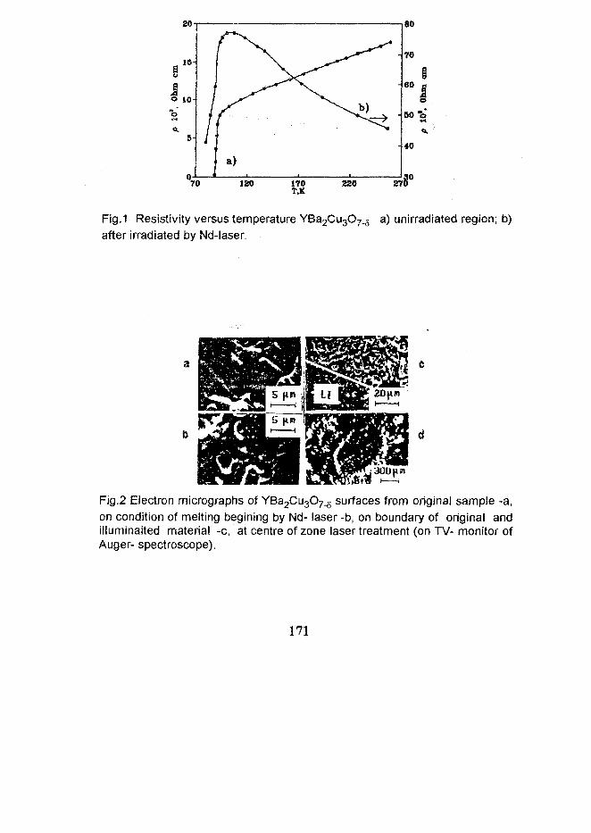
20
70
Fig.1 Resistivity versus temperature YBa2Cu3O7_5 a) unirradiated region; b)after irradiated by Nd-laser.
Fig.2 Electron micrographs of YBa2Cu3O7_6 surfaces from original sample -a,on condition of melting begining by Nd- laser -b, on boundary of original andilluminaited material -c, at centre of zone laser treatment (on TV- monitor ofAuger- spectroscope).
171

Laser irradiation
J J H i U I
Fig.3 Intensity.of K^Cu) and La(Ba) lines along sample from X-ray micro-
probe analysis.
electrical properties, surface morphology and stoichiometry HTSC ceramicsYBa2Cu3O7.5 were determined. These effects can be used forunderstanding the influence of structural disorder and oxygen vacancies onthe superconducting properties, and, possibly, for modifying such properties.
1. E. Adem , L.Martines , J.Rickards et.al., J.Mater.Res.3, 807 (1988).2. A. Iwase, N.Masaki, T. Iwata et.al. Physica C.174,321 (1991).3. M.M. Vasyuk, P.V. Galiy, R.V. Lutciv, Ukr.Phys.Journ.38,1210 (1993).
172

THE CONDITIONS OF THE CRITICAL STATETRANSITION IN THE YREBaCuO (RE;- Pr, Nd)SYSTEM
i mil nunUA9600471
V.A.Voloshin, I.S.Abaiiosheva, G.Yu.Bochkovaya, F.A.Boiko,N.A.Doroshenko, Ya.I.YuzhelevskiiA.Galkin Donetsk Physico-Technical Institute of the National Academy ofSciences of the Ukraine, 340114, Donetsk
The YREBaCuO specimens are superconductive. However, partial substitutionof Y by RE (RE = Nd,Pr) and Ba by RE results in a certain (particular for eachconcentration) decrease in the superconductivity transition temperature (Tc).In this paper we make an attempt to find the parameters which change with thevariation in the impurity ion concentration thus characterizing the temperaturedependence of the electrical resistance of the specimens of the system underinvestigation and determine their superconductive transition. To solve thisproblem it is necessary first of all to provide a mathematically unambiguousdescription (within the framework of the chosen model) of the temperaturedependence of the resistance of the investigated specimens at various REconcentrations.
In specimens with rather high concentration of the RE ions (Figs.l a,b) thetemperature behavior of resistance at high temperature has a metallic charac-ter, i.e. obeys the equation
p ( T ) = / » o + f l T , (1)
where po is the residual resistance in mOhmcm and a is the coefficient in
mOhmcm/K.
As the temperature decreases the type of dependence becomes semiconductive,the character of the resistance growth being close to the exponential lawexp (A E/kT). This character is believed to be due to the presence of potentialwells (traps) in the vicinity of the impurity ions whose depth is characterizedby energy E. At the further temperature decrease the exponential growthterminates and the resistance drops sharply down to zero.
173

300200
Fig.l. Temperature dependence of resistivity of Nd(Ba0 8Nd0 2)2Cu307 (a)and Yo 52Pr0 4gBa2Cu3O7 (b). The experimental data are shown asdots. Curve (1) is calculated using Eq. (2), curve (2) - using equation (2)without the second term. The fit parameters are given in the table.
For the specimens with the lower RE concentration no semiconductive charac-ter of the resistance change is obviously observed but to describe all thespecimens under study the following formula is proposed
po+ccT
1 - l-exp(-AE/kT)] '(2)
where n j is the number of traps with respect to the carrier number (holes). It
is assumed that the trap number is less than the hole number, i.e. 0 < nj< 1
and the trap with the hole inside becomes neutral. The reasons why will beunderstood below.
The second term in Eq.2 whose form coincides with the well- known correctionof Aslamazov and Larkin [1] is introduced for simulation of thesuperconducting transition. And it should be mentioned that no definitephysical sense is attributed to parameter/3.
It is clear that thanks to such big number of fit parameters any particular
174
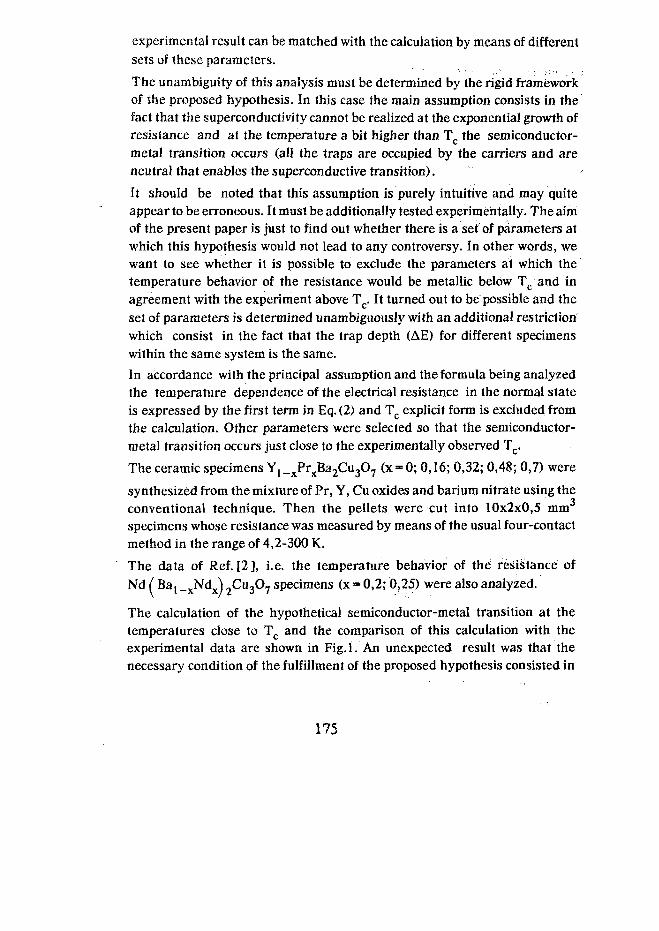
experimental result can be matched with the calculation by means of differentsets of these parameters.
The unambiguity of this analysis must be determined by the rigid frameworkof the proposed hypothesis. In this case the main assumption consists in thefact that the superconductivity cannot be realized at the exponential growth ofresistance and at the temperature a bit higher than Tc the semiconductor-metal transition occurs (all the traps are occupied by the carriers and areneutral that enables the superconductive transition).
It should be noted that this assumption is purely intuitive and may quiteappear to be erroneous. It must be additionally tested experimentally. The aimof the present paper is just to find out whether there is a set of parameters atwhich this hypothesis would not lead to any controversy. In other words, wewant to see whether it is possible to exclude the parameters at which thetemperature behavior of the resistance would be metallic below Tc and inagreement with the experiment above Tc. It turned out to be possible and theset of parameters is determined unambiguously with an additional restrictionwhich consist in the fact that the trap depth (AE) for different specimenswithin the same system is the same.
In accordance with the principal assumption and the formula being analyzedthe temperature dependence of the electrical resistance in the normal stateis expressed by the first term in Eq. (2) and Tc explicit form is excluded fromthe calculation. Other parameters were selected so that the semiconductor-metal transition occurs just close to the experimentally observed Tc.
The ceramic specimens Yj _xPrxBa2Cu3O7 (x = 0; 0,16; 0,32; 0,48; 0,7) were
synthesized from the mixture of Pr, Y, Cu oxides and barium nitrate using theconventional technique. Then the pellets were cut into 10x2x0,5 mm3
specimens whose resistance was measured by means of the usual four-contactmethod in the range of 4,2-300 K.
The data of Ref.[2], i.e. the temperature behavior of the resistance ofNd / BaT _xNdx) 2Cu307 specimens (x = 0,2; 0,25) were also analyzed.
The calculation of the hypothetical semiconductor-metal transition at thetemperatures close to Tc and the comparison of this calculation with theexperimental data are shown in Fig.l. An unexpected result was that thenecessary condition of the fulfillment of the proposed hypothesis consisted in
175

parameter pQ being equal to 0.
Physically these results can be presented in the following way. In a crystalthere are separate rather extended faultless regions isolated from the short-range effects. There are also far-off regions with drastically higher (or lower)electron density which due to the Coulomb interaction create traps for currentcarriers. As the temperature drops the carrier get into the traps, become"frozen" and the potential relief becomes smooth. The conductivity acquiresthe metallic character. The faultless regions where the metallic conductivity isrealized can be represented as the Cu2-O2-O3 planes as is done, for example,in [3 ] and the regions with the electron density deviating from the average onecan be represented by the areas near Pr and Nd ions substituting Ba ions. Thiswill be discussed in detail in our next paper.
Fig.l present the results of the calculations for the specimens of theNd / Baj_xNdx) 2Cu307 system at x = 0,25 and Y1_xPrxBa2Cu307 system
at x = 0,48. The experimental data are shown by dots. The curves in bothfigures were calculated using Eq. (2) with the parameters given in the table withand without the account of the second term, respectively. The figures show thatat the particular set of parameters (X , p and ,AE curves agree with theexperimental data both below Tc and above it, and curves 2 exhibit thesemiconductor-metal transition in the vicinity of Tc. The simultaneousfulfillment of these two conditions turned out to determine unambiguouslythe set of parameters specified in the table.
The similar results were also obtained for the other specimens under study(see the table). The data for the specimens with the praseodimiumconcentrations of 0,32 and 0,16 and also with the excessive neodymiumconcentration of 0,2 can be restored by the parameters given in the table. Theexperimental data correspond almost completely to the curve obtained usingformula (2) and the hypothetical drop of resistance corresponds to the curveobtained by the same formula but at/3 = 0.
In connection with the above considerations some questions arise.
1. Was the semiconductor-metal transition observed near Tc experimentallyin these systems?
According to the data of Ref. [4] (Fig.2) the Meissner effect was, in fact,observed at the lower temperature than the resistance drop onset near Tc
176

2. The specimens with a high content of Pr (x > 0,5) are known to exhibit nosuperconductivity (Fig.3). Do these specimens possess any perfect conductiveregions (i.e. is it possible to describe the temperature dependence of theirresistance within the framework of the accepted formula provided thatparameter p0 is equal to zero) ?
It appears that under these conditions there are no faultless regions. To makean agreement with the experiment nl should be equal to 1 and/>0 be much
greater than 1.
Moreover, it should be noted that within the framework of this papersuppression of superconductivity with the growth of concentration of Pr andexessive concentration of Nd is connected with the magnetic moment of rareearth ions, i.e. the temperature behavior of resistance in both system underinvestigation is described in this work by means of the same formula (2). Forthe Nd system, however, the magnetic properties of the rare earth ion do notalmost effect the resistive properties of the specimens whereas for the Prsystem the mechanism of magnetic pair breaking surely exists. Therefore thecomparison of different mechanism of the resistance suppression requires bothexperimental and theoretical study of these systems.
••/•j
s- 1 . 5 f-
-2,5 [--3.0 i-
1 "~
I?!
A -I
12.0
9,6 O
50
H7.2
-I 2.4i
^ 0.0
s
i W 1 O'J
T (K)Fig.2. Comparison of the temperature dependencies of the Meissner effect
(curve 2, left-hand scale) and resistivity (curve 2, right-hand scale) ofYo 7Pr0 3Ba2Cu307. T (by the data of Ref. [4 ]).
177

1800
Fig.3.
Temperature dependence of resistivityof Yo 3Pr0 7Cu307 . The experimentaldata are shown as dots, the solid line isthe fit one to Eq.(2) with theparameters as given in the Table.
In conclusion the authors express their gratitude to Yu.Kusovlev for hisbrilliant program "Graphical Calculator".
Table. The values of fit parameters for systems Nd ( Baj _xNdx] 2Cu307 and
X ni AEcm"1 mOhmcm
Tc,K mOhmcm
amOhmcm/K
Fig.
Yi-xPrxBa2Cu3O7
0,16
0,32
0,48
0,70
0,58
0,7
0,91
1,00
-85
-85
-85
-17
0,005
0,005
0,018
-
77,5
57,5
35
-
0
0
0
28,00
0,0046
0,0079
0,0078
0
-
-
2
4
Nd(Bai-xNdx)2Cu307
0,20
0,25
0,885
0,9545
-105
-105
0,5
0,5
32,3
9,9
0
0
0,096
0,0155
-
1
178

1. Aslamazov L.J. and A.L.Larkin. Phys.Lett. 26A, 238 (1968).2. Van Woerden R.A.M. and D.M.De Leeuw. Physica C 165, 221, (1990).3. Sukharevskii B. Ya. In "Abstracts of the VI scientific seminar "Physics of
magnetic phenomena", Donetsk, 1993, p. 127.4. Peng J.L., P.Klavins, R.N.Shelton, H.B.Radousky, P.A.Hahn and
L.Bernardez. Phys.Rev. B40, 4517(1989).

*H3HKO-TEXHH4ECKOro H T ^AKA^EMHH HAYK YCCP

A.Galkin Donetsk Physico-Technical Instituteof Ukraine National Academy of Sciences
72, R.Luxembourg St.,Donetsk, 340114, Ukraine.Fax.: (0622) 550-127, (0622) 957-667E-mail: svistuno@sts. dipt, donetsk. uti
The A.Galkin Donetsk Physico-Technical Institute is founded in 1965.
The basic fields of scientific activity are the following:
- physics of magnetic phenomena;
- electron properties of solids and superconductivity.
- physics and technology of high pressures;
The institute proposes the joint research projects including the development ofmaterials with controllable magnetic properties; studies of the structural,electron and thennodynamic properties of high-Tc superconductors; elasticdeformation and destroying of solids under the influence of high hydrostaticpressure; forecasting and controllable modification of rock mass properties forthe development of deep coal seams.
Today in the Institute there are several products of high technology suggestedfor the marketing: precision brasswires of diameter of 0,2-0,4 mm for the toolproduction having the level of exploatation properties equal to the bestproducts worldwide; microfilaments 5-30 pm thick of the steel and othermetals or alloys, and the porous materials on the base of these filaments forthe different purposes; sample sells for the studies in the field ofbarocryomagnetic processing of solids and liquids; microwave electronparamagnetic processing of solids and liquids; microwave electronparamagnetic resonance spectrometers and cryogenic magnet systems.
The Institute proposes the foundation of joint enterprises and associations,license and engineering service, know-how transfer etc. on the bases of thementioned developments.
181

A.GaIkin Donetsk Physico-Technical Institute Ukr.AS72, R.Luxemburg st, Donetsk 340114,UKRAINE
DEPARTMENT of SUPERCONDUCTIVITYand TUNNELING SPECTROSCOPY
Fax: (0622) 55.01.27;E-mail: [email protected]
Head Prof. Vladimir Svistunov
Leading coworkers, Drs: M.Belogolovskii, O.Chernyak, A.D'yachenko,O.V.Grigut', A.Khachaturov, V.Okunev, Yu.Revenko, V.Tarenkov.
Special interest in HTS areas:
CONTACT PHENOMENA as Spectroscopy Methods and DeviceProperties
TRANSPORT PROPERTIES. WIRE,TAPE and FILM SANDWICHFABRICATION
HIGH PRESSURE EFFECT. HTS MECHANISMS
Some Achievements:• Observation and study of Josephson effects - ac, dc and influence of the
different nature fluctuations (Pis'ma Zh.Eksp.Teor.Fiz. 1967,5, p.396;1968, 8, p.521; 1981, 33, Nl, p.274).
«.- Tunnel experiments under pressure: observation of the changes of theenergy gap, the phonon spectra,electron-phonon interaction and quantumsize effects.The creation of the direct method for determining the spectralelectron-phonon interaction function of metals (Sov.Phys.USPEKHI,1987, 30, Nl, p.l; Sov.Phys.JETP, 1974, 39, p.1115; Sov.PhysJETP,1983, 57, p.1038).
• The temperature and pressure dependences of the critical current ofsuperconducting ceramic Ba-Pb-Bi-0 had been studied to know thebarrier pecularities of intergrain boundaries to formation of transportproperties of perovskite-type superconductors. Observation of the mixing
182

effect of rf signals in BaPbBiO ceramic. (Fiz.Nizkikh.Temp., 1985,11,11,p. 1133; Pis'ma Zh.Techn.Fiz. 1986, 12, N14, p.845).
• Experimental evidence for the the superconducting gap and the influenceof the phonon spectrum on the tunneling density state of HTS. Realizationof the persistent currents in the ring type HTcS ceramic samples at 77K.(Fiz.Nizkikh.Temp., 1987,13,N8,P.851.; Pis'ma. Zh.Eksp.Teor.Fiz .3515; Fiz.Nizkikh Temp.1988.14, p.lO95;Physics USPEJCHI, 1993,36, N2,p.65). • '•• : '.•-:- • "''" "?• ';- ^ :; '; , 7 ; J v l
• Discovery of the considerable suppercurrent increase (by two and moretimes) under pressure of HTcSceramics(YBC0,BSC6).The criticalcurrent hysteresis in magnetic fields have. been; .explained (Pis'maZh.Ek'sp/Teor.Fiz., 1988, 47, p.457; §oy.Phys,JETE, 1991, 73(6)p. 1076; Supercond.Sci.Technoi. 1992, 5, p.lOl; Physica C 213, 1993,p.167).
• Observation of the self-energy effects: in film normal state tunnels ofmetaloxides. (Fiz.Tverd.Tela. 1989, 31, N6. p.296; Modern Phys.Lett. B1990,4, N2.p. l l l ) .
• Growth of thin HTS films by Plasma Activation Method (Pis'maZh.Techn.Phys. 1991, 17, N9, p.l; 1993, 19, N5, p.39; 1994, 20, N10,p.60).
Main goals:• Search of the relation between mechanisms of superconducting current
transfer,power dissipation in metaloxide and the technology of thefabrication HTCS materials to increase and maintain Critical Current inHigh Magnetic Fields.The hydroextrusion fabrication of HTCSwires,cables and high-current conductors.
• Contact Phenomena Investigations are focused on the elucidation of thephysical nature of various contributions in the tunnel conductance ofN-I-S, S-I-S and N-I-N junctions to reconstruct the spectral Eliashbergfunction for High-Tc Superconductors.
Our study is being carried out within the framework of the State Pro-gram"HTSC" and is being sponsored and financially supported by the StateCommittee for Science and Technology of Ukraine (projects##0.9.01.:0.1/012-92, 04/065-93, 02/030-94, 01/056-94,04/057-94);
183

DEPARTMENT of SUPERCONDUCTIVITYand TUNNELING SPECTROSCOPY
A.A.Galkin Donetsk Physico-Technical InstituteNational Academy of Sciences of Ukraine
72 R.Luxemburg st , 340114 Donetsk, Ukraine,
Technology Principles for producing long-length wire (including the multi-filament cable) by the hydroextrusion method are elaborated. We havefabricated the laboratory silver-sheathed Bi-2223 wire samples 10 m long and1 -0.3 mm in diameter. The test of current transport properties of these sampleshave revealed the following parameters: Jc = 2.2 • 104 A/cm2 at T=77 K, B = 0andJc =3-103A/cm2 at B = IT; at 4,2 K Jc = 2.4- 105 A/cm2at B = 0andJc =3.1- 104A/cm2 a tB=12T.
The technolology for producing BSCCOfilmsofTc about 80-110 K by the gasdischarge sputtering is developed too. There are possibilities for
a) obtaining glass-like optical YBCO and BSCCO covers
b) measurement of the concentration of the current carries in the region ofmetallic conductivity;
c) estimation of the concentration of metallic phase in the films;
d) determination of Fermi- level of HTS films.
Our study is carried out within the framework of the Ukrainian State HTSProgram according to projects 09.01.04/065-93, 02/030-94, 01/056-94,04/057-94.
We are ready to take part in International Cooperation to continue effectivelyour investigations.
Contact:
Prof.Vladimir M.Svistunov, Head of Department.
Fax: (062 2)55 0127;E-mail:[email protected]
184

AC Susceptibility Studies on HTSC Submicron Films;Ultraweak Magnetic Fields,
Direct and Alternating Transport Current.
The AC susceptibility measurements are essential for the characterizationand analysis of superconducting materials. Specific features of films revealthemselves only in weak magnetic fields. At amplitudes H^ «=? 0.1 - 10 mOe themagnetic flux penetration in the thin film differs from the theoreticalpredictions of the critical state model. With decreasing magnetic field, thediamagnetic screening of submicrori films is enhanced while the quadraturesignal # ' ' drops abruptly and the dissipative loss curve has a fine structure.
Totally new possibilities open up when a film is subjected to the simultaneousaction of ac field and transport current. This method is ideal for testing thinfilms. It is capable to measure the magnetic microstructure and dynamic ofHTSC films
The new experiment of nonlinear induction of magnetic, fjeld byalternating transport current in a film has made it possible: to detect atemperature-dependent response in the resistive region; to suggest a newmethod for accurate determination of the temperature TR-0; to determineindependently the magnitude and temperature dependence of the criticalcurrent; to detect even harmonics of the ac magnetic field in the film.
Our AC Susceptometer measures both the real <x ") and imaginary fy')components of susceptibility as a function of temperature (< 4,2 K to 300 K),amplitude of an ac field (0.1 mOe to 1 Oe) and frequency (1 to 25 KHz) withor without a dc bias field (0 to 5 T). The AC Susceptometer permits to measure:the AC susceptibility signals on a fundamental frequency and on higherharmonics as well; an ac susceptibility signals and R (T) at the same time; aresponse of HTSC films supporting as on direct and alternating current.Theac sensitivity of our AC Susceptometer is 2 *10 emu in term of anequivalent magnetic moment.
V.F.Drobotko and V.A.KhokhlovDonetsk Physico- Technical Institute, Ukrainian Academy of Sciences,R.Luxembourg St., 72, Donetsk, 340114, Ukraine.
Fax.: (0622) 550-127, (0622) 957-667E-mail: [email protected]
185
DEPARTMENT OF SUPERCONDUCTIVITY andTUNNELING SPECTROSCOPY
A.A.Galkin Donetsk Physico-Technical Institute
SOME PUBLICATIONS
Review papers:
1. V.M.Svistunov.M.A.Belogoiovskii and A.I.D'yachenko.Elastic tunnelingspectroscopy of single-particle excitation in metals, J. Low Temp.Phys.,1978,31,p.339.
2. V.M.Svistunov and M.A.Belogolovskii. Tunneling spectroscopy ofquasiparticle excitations in metals (monograph), Naukova Dumka, Kiev,in Russian, 1986.
3. V.M.Svistunov, M.A.Belogolovskii and O.I.Chernyak. Tunnel investigationsof metals at high pressures. Usp.Fiz.Nauk, 1987,151, Nl,p.31; Sov.Phys.USPEKHI, 1987, 30, Nl .p . l .
4. V.M.Svistunov.M.A.Belogolovskii and A.I.D'yachenko. Vacuum tunnelingmicroscopy and spectroscopy. Usp. Fiz. Nauk, 1988, 154, Nl, p. 153; Sov.Phys. USPEKHI, 1988, 31, Nl, p.86.
5. V.G.Baryakhtar, I.D'yachenko,V.M.Svistunov. A Kinetic properties ofceramic superconductors as a Josephson medium / / In : "High-Tc
superconductivity" ed. by A.S.Davydovand V.M.Loktev, Springer-Verlag,Berlin, 1992. p. 136-149.
6. V.M.Svistunov, M.A.Belogolovskii and A.I.Khachaturov. Electron-phononinteraction in High-Tc Superconductors. Usp. Fiz. Nauk, 1993. 163, N2.p.1-19; Physics USPEKHI, 1993, 36, N2, p.65.
7. V.M.Svistunov, I.Iguchi, A.Belogolovskii and A.I.Khachaturov. SomeFeatures of Electron Tunneling in the Normal and Superconductive Stateof HTS. Modern Phys. Lett. B, 1994, 8, p.407-424.
186

Other papers(HTS):
8. V.M.Svistunov and Yu.F.Revenko. Mixing effect of rf signals in BaPbBiOceramics, Pis'ma Zh. Techn. Fiz., 1986, 12, N14, p.845.
9. V.M.Svistunov, A.I.Khachaturov, M.A.Belogolovskii, V.Yu.Tarenkov. Apossible observation of localization effects in the metal oxides by theelectron tunneling method. Fiz. Nizkikh Temp, 1988, 14, Nl. p.101.
10. V.M.Svistunov, V.Yu.Tarenkov, A.I.D'yachenko, O.I.Chernyak. Electriccharacteristics of Ag-YBaCuO System / / Pis'ma Zh. Eksp. Teor. Fiz. 1989,49, Nll,p.614.
11. V.M.Svistunov, A.I.Khachaturov, M.A.Belogolovskii, I.V.Kochergin,S.Benacka, A.Plecenik, S.Cuomik. Tunneling and resistive studies of thenormal state properties of YBCO thin films / Modern Physics Letters B,1990, 4,N2, p.111-118.
12. A.I.D'yachenko, A.A.Kvachev, I.V.Kochergin and V.M.SvistunovProbable role of high-freguency modes in high-Tc superconductors / Phys.Lett. A, 1990,150, N2, p.121-125.
13. V.M.Svistunov, A.I.D'yachenko, V.Yu.Tarenkov / Pressure effects onhigh-Tc superconductor current transfer / / Intern.Rev.Mod.Phys., 1991.5, N20, p.3255-5365.
14. V.M.Svistunov, V.Yu.Tarenkov, A.I.D'yachenko and O.I.Cherhyak.Effects produced by the Josephson medium during tunneling in metaloxides. Sverkhprovodimost' (KIAE), 1991, 4 (6), p.1144-1148
15. V.M.Svistunov, Yu.F.Revenko, O.V.Grigut', M.A.Belogolovskii andA.I.Khachaturov. Effect of weak and srtong localization in HTSCtunneling characteristics / / Superconductivity: physics, chemistry,technology, 1992. N7, p.1218.
16. M.Grajcar, A.Plecenic, S.Benacka, Yu.F.Revenko and V.M.Svistunov.Time evolution of point contact resistances of HTS. Physica C, 1993, 218,p.82.
17. V.D.Okunev, N.N.Pafomov, Z.A.Samojlenko and V.M.Svistunov.Competition of superconducting 2212 and 2223 phases for amorphousstate-cristal transition in BiPbSrCaCuO films (Pisma v Zhurnaltekhnicheskoi fiziki. 1994, 20, p. 60-65).
187

AUTHOR INDEX
Abalioshev A.V.
Abaliosheva I.S.
Afanassyev D.N.
Aoki R.
Babenko V.V.
Belevtsov L.V.
Belogolovskii M.A.
Bochkovaya G.Yu.
Boiko F.A.
Boiko Ya.V.
Boot'ko V.Y.
Bush A.A.
88,166
173
66,71,80
17
133
95
44,80
173
173
116,166
133
125
Dou S.X.
Drobot'ko V.F.
Ekino T.
Ermolina S.I.
Esparza D.A.E
Fiscina J.E.
Fujii H.
Gabovich A.M.
Gogadze G.A.
Gonzalez Oliver
Gordeev S.N.
103
107
25
100
121,129
121
25
29,32
36
CJ.R. 121
125
Caplin D. 103
Chabanenko V.V. 97,100
Cherenkov O.P.I 44
Cohen L.E. 103
Iguchil. 40,53,71,80,139
Jahn W. 125
D'yachenkoA.I. 21,88,112
DanylivO.D. 84
De Bruyn Ouboter R. 57
Doroshenko N.A. 173
KhachaturovA.I. 44,80
Khokhlov V.A. 107
Kisel N.G. 100
KitaT. 17
188

Klestov S.A.
Koops M.C.
Kovylyaev V
Krans J.M.
Krynetskii I.
KupferH.
.V.
B.
103
57
150
49
97
125
Kvitnitskya O.E. 61
LaceyD. 103
Lee K. 80,53,80
Leszczy n skii J. 147
LomaevaS.F. 154
LutcivR.V. 116,166,169
Malachevsky M.T
Matviiv M.V.
Melnikov V.S.
Menovsky A.A.
Mikheenko P.M.
Minami T.
Ming Xu
Moshchil V.E.
Muller C.J.
Murakami H.
. 129
116
150
61
133
25
103
150
57
17
Nagorny P.A. 150
NaidyukYu.G. 61
Nebogatikov N.M. 154
NishioY. 17
NbwackA. 61
MysoedovYu.N. 116,166
OkunevV.D.
Pafomov N.N.
Pashchenko V.P.
Perekrestov B.I.
Perkins G.
Peters E.T.
Piechota S.
Poritski R.M.
Prikhna T.A.
Pushenko E.I.
RevenkoYu.F.
Reznikl.M.
Roizenblat E.M.
Rumyantsev V.V.
Samoilenko Z.A.
Shabanova I.N.
ShevchenkoS.S.
Shirai M.
71,139,157
139,157
144
139,147
103
62
97,100
144
150
157
66,71
133
100
76
157
154
95
17
189

Shtaerman E.Ya.
ShvaikaA.M.
Solovyov V.F.
Stasyuk I.V.
Strekalova E.P.
Sukharevskii B.Ya.
Svistunov V.M.
Szymczak H.
76
84
150
84
144
160
11,71,139
97,100
Vasilenko A.V.
Vasyuk M.M.
Vleeming B.J.
Voitenko A.I.
Voloshin V.A.
Voronkova V.I.
Wang Q.
147
169
57
32
133,173
103
40
TarenkovV.Yu. 88,166
TerebovaN.S. 154
TuytuynnikV.B. 144
Yansonl.K. 49,61,62
Yoshida K. 40
Yuzhelevskii Ya.I. 133,173
Van der Post N. 62
VanRuitenbeekJ.M. 49,62
Zhukov A.A. 125
190