
Micromachined high frequency PMN-PT/Epoxy 1–3 composite ultrasonic annular arrays
Upload
independentCategory
view
4download
0
Nuclear Instruments and Methods in Physics Research A 442 (2000) 443}451
Silicon-micromachined microchannel plates
Charles P. Beetz!,1, Robert Boerstler!, John Steinbeck!,Bryan Lemieux", David R. Winn",*
!NanoSciences Corporation, 83 Prokop Road, Oxford, CT 06478, USA"Fairxeld University, Department of Physics, Fairxeld, CT 06430-5195, USA
Abstract
Microchannel plates (MCP) fabricated from standard silicon wafer substrates using a novel silicon micromachiningprocess, together with standard silicon photolithographic process steps, are described. The resulting SiMCP microchan-nels have dimensions of &0.5 to &25 lm, with aspect ratios up to 300, and have the dimensional precision and absenceof interstitial defects characteristic of photolithographic processing, compatible with positional matching to siliconelectronics readouts. The open channel areal fraction and detection e$ciency may exceed 90% on plates up to 300 mm indiameter. The resulting silicon substrates can be converted entirely to amorphous quartz (qMCP). The strip resistanceand secondary emission are developed by controlled depositions of thin "lms, at temperatures up to 12003C, alsocompatible with high-temperture brazing, and can be essentially hydrogen, water and radionuclide-free. Novel secondaryemitters and cesiated photocathodes can be high-temperature deposited or nucleated in the channels or the "rst strikesurface. Results on resistivity, secondary emission and gain are presented. ( 2000 Elsevier Science B.V. All rightsreserved.
1. Introduction:
Glass microchannel plates (MCP) su!er fromoperation and fabrication at relatively low temper-atures (precluding most CVD activation or brazedmountings), evolution of hydrogen ions from thesurface (potential photocathode degradation), gaindegradation, and short gain-lifetime at high inci-dent electron #uxes [1,2]. Spatial defects due to the"ber-bundling process lower the e!ective spatialresolution and image uniformity and limit the abil-ity to couple the MCP to silicon-device readouts,and pixel sizes are usually larger than &5}6 lm
*Corresponding author. Tel.: #1-203-254-4000; fax: #1-203-254-4277.
E-mail address: [email protected] (C.P. Beetz),[email protected]"eld.edu (D.R. Winn)
1www.nanosciences.com.
for commercially viable products. Relatively lowpore areal packing fractions ((60}65% openpores) create an upper limit on detection e$ciency,near this areal open fraction. Glass MCP areself-radioactive and non-radiation hard at levelsincompatible with some very low light or spaceapplications. Lastly, they are expensive and un-available in very large image formats. We havetherefore looked at silicon micromachining todevelop a new type of Si- and quartz-MCP materialssystems, which can take advantage of the massproduction technologies developed by the semi-tool and semiconductor industry.
2. Silicon MCP substrates
Silicon microchannel plates (SiMCP) have beenfabricated using a photolithographically initiated
0168-9002/00/$ - see front matter ( 2000 Elsevier Science B.V. All rights reserved.PII: S 0 1 6 8 - 9 0 0 2 ( 9 9 ) 0 1 2 7 1 - 1

Fig. 1. Micromachined microchannel matrix for a precisionSiMCP, fabricated at NanoSciences Corporation. The squarechannels are on a 6 lm spacing, with a side dimension of 3 lm.The top surface has been micromachined to a tapered bladepoint to enhance the collection e$ciency of incident photo-electrons; approximately 95% of the surface is open.
proprietary micromachining process developed atNanoSciences Corporation (NSci). The placement,size and pore uniformity of the silicon MCP sub-strate channels therefore have dimensional pre-cisions greatly exceeding that of glass-"ber-basedMCP. Figs. 1}4 show SEM micrographs of fourdi!erent forms of these substrates, and Fig. 5a}cshow optical photographs of the SiMCP. The com-plete elimination of MCP defects (for example, dueto misplacement or defomation of the glass "bers ina boule) is achievable, and the microchannel out-puts can be placed with precision with respect topotential lithographically patterned readouts. Porediameters are fully adjustable between 0.5 and25 lm, with high aspect ratios (a"holelength/hole diameter) } up to 300:1 has beenachieved with 3 lm holes } a possible theoreticallimit is a'2000:1. Large SiMCP diameters arepossible, up to the size of available silicon wafers} limited with presently commercially viable siliconwafers to &30 cm (12A) diameter SiMCP plates. Atpresent, SiMCP of 10 cm diameter have been pro-duced at NSci, limited only by the installed photoli-thographic equipment (4A wafer fab). The holes canbe square, and '90% open area; micromachiningcan taper the hole entrances as shown in Fig. 1.These SiMCP substrates can be vacuum-baked attemperatures &12003C, and brazed at similarelevated temperatures, much hotter than those pos-sible with glass MCP, or converted entirely orpartially to oxide (amorphous quartz } qMCP) foreven higher-temperature processing. Chevroningup to 83 to the surface plane have been demon-strated, as shown in Fig. 4.
3. Electrical isolation, strip resistance, andsecondary emission coatings
Because of these temperature characteristics andthe silicon-based substrate, CVD processes can beused to activate the SiMCP or qMCP plates withanhydrous, high-temperature secondary-emissionmaterials or with photocathodes. Since silicon issemiconducting and has a relatively small bandgap &1.07 eV, it is not possible to develophigh enough electric "elds in the channels forgenerating electron gain. Even for intrinsic silicon
444 C.P. Beetz et al. / Nuclear Instruments and Methods in Physics Research A 442 (2000) 443}451

Fig. 2. Left. Edge view of the cross-section of a dense array of 6 lm channels with the micromachining process halted 368 lm intoa 520 lm thick silicon wafer, the channels are spaced on 8 lm centers; Right: top view of the wafer showing the 6 lm wide channelopenings.
Fig. 3. Cross-section views of a section of an extremely thin-wallsilicon SiMCP substrate converted to amorphous quartz. Notethat the walls in the channels are extremely smooth; more than90% of the silicon is removed. Fiducial bar"2.5 lm
whose resistivity is &104 ) cm, the resistance ofa 1 cm2, 0.36 mm thick plate silicon MCP having6 lm2 channel openings on 8 lm centers, a"60(for example), would draw about 1200 W at 1 KV.Therefore, bare silicon plates cannot be used due toexcessive conductivity.
A strategy of coating the silicon with an insulat-ing coating, then a strip resistance layer and thena secondary emission layer has been employed tocircumvent this problem. A schematic diagram of
the coatings necessary for reproducing the func-tionality of the reduced lead glass microchannelplate surface is shown in Fig. 6. The insulating layerprovides the isolation necessary to keep the gener-ated secondary electrons from being shunted by theconducting silicon substrate. The strip resistance isa weakly conducting layer that re-supplies chargeto the secondary emission layer to maintain thesecondary electron gain.
The isolation layer strategy was initially dis-cussed by Tasker et al. [3,4] in the development ofsilicon-based MCP and as for coatings for single-channel multipliers. They developed a successfulcoating system for quartz tube single-channelmultipliers that employed a slightly oxidized poly-silicon layer that provided both the strip resistanceand secondary emission surface. Electrical isolationand strip resistance of the silicon MCP is accomp-lished using a two-step isolation procedure. Sincethe Si-MCP substrate is conductive, the stripresistance layer must "rst be insulated from theSi substrate as illustrated in Fig. 6. The isolationcan be accomplished by thermally oxidizing the Si-MCP substrate and/or depositing an insulatinglayer. The insulating layer thickness depends on thebias voltage stand-o! required. After the SiMCPsubstrate wafer has been diced into the desiredSiMCP shapes, they are inserted into a high-tem-perature wet oxygen oxidation furnace to growa thick (&1 lm or more) oxide layer on the top
C.P. Beetz et al. / Nuclear Instruments and Methods in Physics Research A 442 (2000) 443}451 445

Fig. 4. Elevation (top) and Plan (bottom) views of a partiallycompleted p-type silicon wafer SiMCP substrate using Nano-Sciences' proprietary high-aspect ratio high rate silicon micro-machining processes. The 10 lm on 11.25 lm pitch SiMCPchannels are chevroned at about 83 to the wafer surface plane.
surfaces of the outer frame of the device as well ason the walls of the channels in the device. Specialpost-processing deposition is also used to forma frame for mechanically handling the SiMCP,whilst maintaining surface #atness. The siliconoxidsing can be complete, forming a quartz MCP(qMCP), or partial, preserving an optically opaquechannel wall (other applications).
The strip resistance for single-channel electronmultipliers that are typically &1 lm in diameterand &60 lm in length needs to be &108 )'s [3,4].For a strip resistance layer &0.1 lm in thickness,
the resistivity needs to be &50 ) cm, a value thatis straight forward to obtain by chemical vapordeposition. In contrast, for example, a square cmSiMCP of 6 lm2 microchannels on 8 lm centers,360 lm long with a &0.1 lm thick strip resistancelayer, requires the polysilicon layer to have a resis-tivity of &108 ) cm since the resistance of theindividual channels are all in parallel with oneanother. Polysilicon can be deposited having resis-tivity over the range 1}107 ) cm using plasmachemical vapor deposition [5], reactive sputtering[6] and electron beam evaporation [7]. Coatingsbased on CVD techniques are desired since uniformcoatings can be produced on channels of high as-pect ratio. It is possible to deposit very high resis-tivity amorphous Si and extremely "ne grainpolysilicon "lms by CVD, and doping with nitro-gen and/or oxygen. Films having resistivity on theorder of 1010 ) cm have been achieved using thethermal decomposition of dichlorosilane in ammo-nia at temperatures &8503C. Uniform coatingsare also readily achieved on high-aspect ratio chan-nels ¸/d'60 employing low-pressure depositionatmospheres &10}500 mTorr.
A cross-section through a wall of some processedSi-MCP are shown in Figs. 7 and 8 . The cross-section shows the Si core that remains after partialthermal oxidation, and the polysilicon coating thatprovides the strip resistance. The oxide was grownby thermal oxidation in a #owing atmosphere ofwater vapor in oxygen [8]. The polysilicon can alsobe doped with nitrogen; a thin deposit of siliconnitride helps enable the smooth nucleation of thepolycrystalline Si/SiO
x"lm on the SiO
2layer.
A thick silicon nitride interfacing layer is shown inFig. 9 (note that silicon nitride also has a high SEyield). An I}< curve for a low-current doped poly-silicon-coated Si-MCP substrate &2 cm diameteris shown in Fig. 10, compared with other glassMCP; much higher or lower plate resistances areeasily possible.
Secondary emission is obtained from thin "lmsof SiO
2and SiO
x(as in normal lead glass MCP)
although CVD nucleating on silicon, silicon diox-ide or silicon nitride o!ers many other high perfor-mance alternative SE materials systems, such assilicon silicides, metal oxides, diamond, GaP orcesiated semiconducting materials, to be described
446 C.P. Beetz et al. / Nuclear Instruments and Methods in Physics Research A 442 (2000) 443}451

Fig. 5. Fig. 5(a,b). Photographs of a 4A (10 cm) silicon wafer with a full array of micromachined pores. Left: back-illuminated, showingthe light transmission in air. Right: #ash-illuminated showing the di!raction pattern from the holes. (c). Diced-out 1 cm]1 cm SiMCPsection, back-illuminated with a spotlight.
Fig. 6. Illustration of the coating system necessary on a silicon-based MCP in order to replicate the functionality of the surfacelayers on a reduced lead glass-based MCP.
elsewhere. An optimized 10 nm thick Si/SiOx"lm
will reach a peak SE yield of 3.5}4 betweeen 300and 400 eV incident [9}11]; the thin SE "lms de-posited to date exhibit SE behavior vs. incidentelectron energy as shown in Fig. 11. The gain ina silicon microchannel of a SiMCP has been mea-sured using an electron microscope electron beamand is shown in Fig. 12, compared with theoretical
C.P. Beetz et al. / Nuclear Instruments and Methods in Physics Research A 442 (2000) 443}451 447

Fig. 7. Cross-sections through a single-channel wall of a frac-tured, processed SiMCP plate showing the silicon core, thermaloxide and CVD-deposited polysilicon and SiO
xcoatings in the
silicon MCP structure. The resistivity of the polysilicon "lm was85]106 ) cm.
Fig. 8. Cross-sections through the channel walls of a fractured,processed Si-MCP substrate showing the layers deposited onthe wall surface, similar to Fig. 7, illustrating the #at, opaque Sicore pro"le, encased in the partial silcon oxide. (Orientation 903from previous "gure. Defect on right is a debris particle fromfracturing.)
Fig. 9. Cross-sections through a single-channel wall of a frac-tured, processed SiMCP plate showing the thermal oxide andCVD-deposited polysilicon, thick silicon nitride and SiO
xcoat-
ings in the Nsci SiMCP structure.
values calculated from the applied voltage, mea-sured SE yield data, and the pore aspect ratio a as
G"(A</2a<1@20
)c (1)
with
c"4a2(<0/<) (2)
and A given by the SE yield data d from
d"A<1@2#
, (3)
and < is the total channel voltage, <0
is the initialenergy of the secondary electron,&1 eV. (The gainmay be somewhat low due to saturation from usingan SEM electron beam for the incident electrons.)
The absence of water or hydrogen in the SiMCPmaterials system may help with electro-optic devicelongevity (especially the photocathode) when usingthese silicon-based MCP, in contrast to glass-basedMCP. Lifetime tests are not complete; however,SiMCP are repeatably able to cycle between airand vacuum with little change in performance.
The silicon can also be fully oxidized to amorph-ous quartz, for SE activation processing or stripresistance processing up to 14003C.
3.1. Image tube
A silicon MCP has been installed in a cesiatedphotocathode imaging tube, and have demon-strated spatial resolution of at least 89 lp/mm } lim-ited by the resolution of the readout. Fig. 13 showsa tube assembly and the imaged test pattern.
448 C.P. Beetz et al. / Nuclear Instruments and Methods in Physics Research A 442 (2000) 443}451

Fig. 10. The I}< characteristics of a Galileo and Philips glass MCPs along with an example of a Si-MCP, shown on a semi-log plot fordirect comparison (vertical scale"nA). E!ective resistance characteristics both higher and lower for the SiMCP have been achieved.Note the similarity in the curvatures.
Fig. 11. Secondary electron yield measured as a function of the incident electron energy for CVD deposited polysilicon/SiOx"lms
having various resistivities and post-deposition heat treatments.
C.P. Beetz et al. / Nuclear Instruments and Methods in Physics Research A 442 (2000) 443}451 449
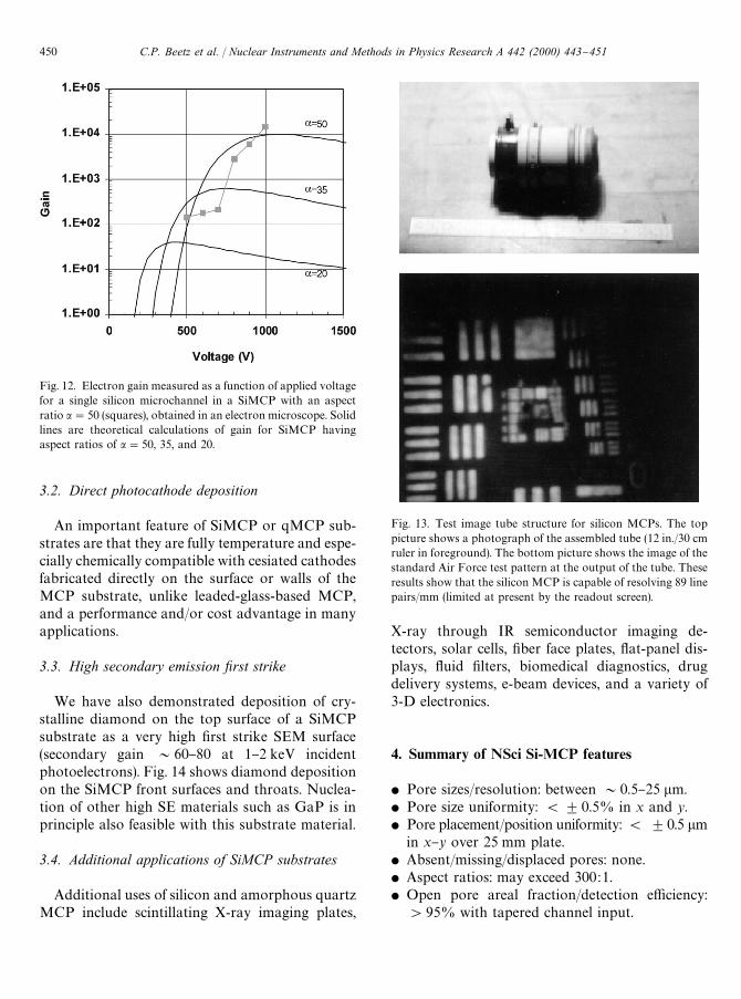
Fig. 12. Electron gain measured as a function of applied voltagefor a single silicon microchannel in a SiMCP with an aspectratio a"50 (squares), obtained in an electron microscope. Solidlines are theoretical calculations of gain for SiMCP havingaspect ratios of a"50, 35, and 20.
Fig. 13. Test image tube structure for silicon MCPs. The toppicture shows a photograph of the assembled tube (12 in./30 cmruler in foreground). The bottom picture shows the image of thestandard Air Force test pattern at the output of the tube. Theseresults show that the silicon MCP is capable of resolving 89 linepairs/mm (limited at present by the readout screen).
3.2. Direct photocathode deposition
An important feature of SiMCP or qMCP sub-strates are that they are fully temperature and espe-cially chemically compatible with cesiated cathodesfabricated directly on the surface or walls of theMCP substrate, unlike leaded-glass-based MCP,and a performance and/or cost advantage in manyapplications.
3.3. High secondary emission xrst strike
We have also demonstrated deposition of cry-stalline diamond on the top surface of a SiMCPsubstrate as a very high "rst strike SEM surface(secondary gain &60}80 at 1}2 keV incidentphotoelectrons). Fig. 14 shows diamond depositionon the SiMCP front surfaces and throats. Nuclea-tion of other high SE materials such as GaP is inprinciple also feasible with this substrate material.
3.4. Additional applications of SiMCP substrates
Additional uses of silicon and amorphous quartzMCP include scintillating X-ray imaging plates,
X-ray through IR semiconductor imaging de-tectors, solar cells, "ber face plates, #at-panel dis-plays, #uid "lters, biomedical diagnostics, drugdelivery systems, e-beam devices, and a variety of3-D electronics.
4. Summary of NSci Si-MCP features
f Pore sizes/resolution: between &0.5}25 lm.f Pore size uniformity: ($0.5% in x and y.f Pore placement/position uniformity: ($0.5 lm
in x}y over 25 mm plate.f Absent/missing/displaced pores: none.f Aspect ratios: may exceed 300:1.f Open pore areal fraction/detection e$ciency:
'95% with tapered channel input.
450 C.P. Beetz et al. / Nuclear Instruments and Methods in Physics Research A 442 (2000) 443}451

Fig. 14. Diamond surface deposits on Si-MCP substrates to enhance "rst strike gain. The left photo shows a plan view of the coatedsubstrate and the right photo shows a cross-section through the MCP walls illustrating the tapering of the deposit. At 1}2 kV, theboron-doped diamond has gain between 60 and 80.
f Plate sizes: to 90 mm diameter now, extendableto &300 mm (12A wafer substrates).
f Chevron: up to 83 tilt demonstrated.f Bake-out temperatures: (12003C SiMCP,
(14003 Q-MCP.f Plate resistance/current: adjustable from
1 K)}10 M)/cm2.f Activation processes: CVD, electroplating, gas,
liquid and phase reactants (others).f SE materials: silicon oxides, metal oxides and
silicides, diamond, GaP (others).f Compatible with direct-front-surface deposited
cesiated photocathodes.f Compatible with high-temperature deposition of
high SE "rst strike materials.f Compatible with high-temperature metal/ce-
ramic brazing.f Low or negligible hydrogen or water content.f Low or negligible self-radioactivity possible.f High radiation resistance.f Fully compatible with silicon lithographically
patterned readout, silicon processing.
f Fully or partially oxidizable to amorphousquartz.
f Gain: comparable to leaded-glass MCP.f Optically opaque channel walls if not fully oxi-
dized.
References
[1] B. Sandel et al., Appl. Opt. 16 (1977) 1435.[2] F. Bennett, D. Thorpe, J. Phys. E 3 (1970) 241.[3] G.W. Tasker, J.R. Horton, J.J. Fijol, Mater. Res. Soc. Proc.
192 (1990) 459.[4] G.W. Tasker, J. R. Horton, US Patent 5,378,960, 1995.[5] P. Sichanugrist, T. Yoshida, Y. Ichikawa, H. Sakai, J.
Non-Cryst. Solids 164 (1993) 1081.[6] W.T. Pawlewicz, J. Appl. Phys. 49 (1978) 5595.[7] J. Sangrador, I. Esquivias, T. Rodriguez, J. Sanz-Maudes,
Thin Solid Films 125 (1985) 79.[8] G. Tasker et al., SPIE Proc. V2640 (1995) 58.[9] H. Seiler, J. Appl. Phys. 54 (11) (1983) R1.
[10] J. Fijol et al., Appl. Surf. Sci 48/49 (1991) 464.[11] G. Tasker et al., Thin-"lm amorphous silicon dynodes for
electron multiplication, MRS Symposium, Vol. 192, (1990),459 p.
C.P. Beetz et al. / Nuclear Instruments and Methods in Physics Research A 442 (2000) 443}451 451
Copyright © 2022 FDOKUMEN