Microcontroller Compensated Micromachined Oscillator Circuit
133
Microcontroller Compensated Micromachined Oscillator Circuit Senior Design II Project Document Department of Electrical and Computer Engineering University of Central Florida Dr. Lei Wei Group 13: Megan Driggers - Electrical Engineering Heather Hofstee - Electrical Engineering Michaela Pain - Computer Engineering Project Sponsor: Dr. Reza Abdolvand, UCF ECE Associate Professor April 20, 2019
-
Upload
khangminh22 -
Category
Documents
-
view
1 -
download
0
Transcript of Microcontroller Compensated Micromachined Oscillator Circuit
Microcontroller Compensated Micromachined
Oscillator Circuit
Senior Design II Project Document
Department of Electrical and Computer Engineering
University of Central Florida
Dr. Lei Wei
Group 13:
Megan Driggers - Electrical Engineering
Heather Hofstee - Electrical Engineering
Michaela Pain - Computer Engineering
Project Sponsor:
Dr. Reza Abdolvand, UCF ECE Associate Professor
April 20, 2019

i
Table of Contents
1. Executive Summary ......................................................................................................1
2. Project Description ........................................................................................................2
2.1 Background ..............................................................................................................2
2.2 Motivation ................................................................................................................3
2.3 Deliverable Requirements ........................................................................................4
2.4 House of Quality ......................................................................................................4
2.4.1 Engineering Requirements .............................................................................5
2.4.2 Product Requirements ....................................................................................5
2.5 Overall Project Responsibilities ...............................................................................5
3. Project Research and Component Selection ...............................................................7
3.1 Resonator .................................................................................................................7
3.2 Zero TCR Resistor ...................................................................................................7
3.2.1 Choosing Series for Comparison ...................................................................8
3.2.2 Y16285R00000D0W .....................................................................................8
3.2.3 Y1625100R000Q9R ......................................................................................9
3.2.4 Y402310R0000C9R .......................................................................................9
3.2.5 Y1630250R000T9R .......................................................................................9
3.2.6 Y11191R00000D9W .....................................................................................9
3.2.7 Y162910R0000C9R .......................................................................................9
3.2.8 Series Selection ..............................................................................................9
3.3 Microcontroller ........................................................................................................9
3.3.1 Communication Interface .............................................................................10
3.3.1.1 Serial Communication ..................................................................11
3.3.1.2 Parallel Communication ...............................................................11
3.3.1.3 Communication Interface Selection .............................................11
3.3.2 Accuracy ......................................................................................................12
3.3.3 MSP430 Series .............................................................................................12
3.3.4 MSP432 Series .............................................................................................12
3.3.5 PIC24F Series ..............................................................................................13
3.3.6 Gecko Series ................................................................................................13
3.3.7 Series Selection ............................................................................................13
3.4 Liquid Crystal Display ...........................................................................................15
3.4.1 Choosing Series for Comparison .................................................................16
ii
3.4.2 LCM-H01604DSF .......................................................................................18
3.4.3 EA 8081-A3N ..............................................................................................18
3.4.4 TC1602A-09T ..............................................................................................19
3.4.5 NMTC-S20200BMNHSGW-12 ..................................................................19
3.4.6 LCD-20x4Y .................................................................................................19
3.4.7 NHD-0216K1Z-FL-YBW............................................................................19
3.4.8 Series Selection ............................................................................................19
3.5 First Order Filter ....................................................................................................20
3.6 Instrumentation Amplifiers ....................................................................................21
3.6.1 Choosing Series for Comparison .................................................................22
3.6.2 ISL28635......................................................................................................24
3.6.3 AD8422 ........................................................................................................24
3.6.4 AD8428 ........................................................................................................24
3.6.5 INA828 ........................................................................................................24
3.6.6 INA128 ........................................................................................................25
3.6.7 INA217 ........................................................................................................25
3.6.8 Final Selection .............................................................................................25
3.6.9 Measure Voltage Across Resonator .............................................................25
3.6.10 Measure Voltage Across 10Ω Resistor ..................................................26
3.7 Voltage Regulator ..................................................................................................26
3.7.1 Choosing Series for Comparison .................................................................27
3.7.2 LM317..........................................................................................................28
3.7.3 NCP110 ........................................................................................................28
3.7.4 MAX15006 ..................................................................................................29
3.7.5 TLS115D0EJXUMA1 .................................................................................29
3.7.6 NCP786AMNADJTBG ...............................................................................29
3.7.7 TS31023 .......................................................................................................29
3.7.8 Final Selection .............................................................................................29
3.8 Potentiometer .........................................................................................................30
3.8.1 Choosing Series for Comparison .................................................................31
3.8.2 P120PK-Y25BR10K ....................................................................................32
3.8.3 3590S-2-103L ..............................................................................................32
3.8.4 534B1502JC .................................................................................................32
3.8.5 RK09K1130A8G .........................................................................................32
3.8.6 3386P-1-105 .................................................................................................32
iii
3.8.7 774-284TBCF504A26A1 ............................................................................33
3.8.8 Final Selection .............................................................................................33
3.9 Switches .................................................................................................................33
3.10 Power Supply .........................................................................................................34
3.11 Software Tools .......................................................................................................34
3.11.1 Communication ......................................................................................34
3.11.1.1 Microsoft OneDrive ....................................................................34
3.11.1.2 CCS Cloud ..................................................................................35
3.11.2 Development ..........................................................................................35
3.11.2.1 Integrated Development Environment ........................................35
3.11.2.2 Programming Language ..............................................................35
3.11.2.3 EAGLE .......................................................................................36
3.11.3 Documentation .......................................................................................36
3.11.3.1 Microsoft Word ..........................................................................36
4. Design Requirement Specifications, Constraints, and Standards ..........................37
4.1 Design Requirement Specifications .......................................................................37
4.1.1 Frequency .....................................................................................................37
4.1.2 Resistance ....................................................................................................38
4.1.3 Display .........................................................................................................38
4.1.4 Modes of Operation .....................................................................................38
4.1.5 Accuracy ......................................................................................................38
4.2 Design Constraints .................................................................................................38
4.2.1 Economic, Manufacturability, and Sustainability ........................................38
4.2.2 Social, Political, and Ethical ........................................................................39
4.2.3 Environmental, Health, and Safety ..............................................................39
4.3 Standards ................................................................................................................39
4.3.1 Safety Standards...........................................................................................39
4.3.2 Testing Standards .........................................................................................40
4.3.3 Operating Standards .....................................................................................40
4.3.4 Software Standards ......................................................................................40
4.3.4.1 Standard SystemC Language Reference Manual Standard ..........40
4.3.4.2 Design Impact of Standard SystemC Language ...........................40
4.3.4.3 Software Testing Standard ............................................................41
4.3.4.4 Design Impact of Software Testing Standard ...............................42
4.3.4.5 C Standard ....................................................................................43

iv
4.3.4.6 Design Impact of C Standard ........................................................43
5. Project Design ..............................................................................................................45
5.1 Analog Schematic Design in LTSpice XVII .........................................................45
5.2 Digitally Controlled Schematic Design in LTSpice XVII .....................................47
5.3 Schematic Design in Autodesk Eagle ....................................................................49
5.3.1 Circuit Inputs ...............................................................................................50
5.3.2 Circuit Outputs .............................................................................................51
5.3.3 Adding Libraries ..........................................................................................51
5.4 Final Schematic Design .........................................................................................51
5.4.1 Voltage Reference ........................................................................................52
5.4.2 Interface .......................................................................................................53
5.4.3 Push Buttons and Program Reset .................................................................53
5.4.4 Microcontroller ............................................................................................54
5.4.5 Display .........................................................................................................56
5.4.6 Relay Operation ...........................................................................................57
5.5 DC-to-DC Power Conversions ..............................................................................57
5.5.1 Main Power Supply (10V) to Microcontroller (3.3V/2mA) ........................58
5.5.2 Main Power Supply (10V) to LCD Screen (5V/35mA) ..............................58
5.5.3 Main Power Supply to Biasing Voltage.......................................................59
5.6 Printed Circuit Board Hardware Power Requirements ..........................................60
5.6.1 Main Power Supply......................................................................................60
5.6.2 Instrumentation Amplifiers ..........................................................................60
5.6.3 Voltage to Current Converter.......................................................................60
5.6.4 Overall Voltage Supply Design ...................................................................61
5.6.5 Power Supply for Components ....................................................................61
5.7 Designing the PCB in Eagle ..................................................................................62
5.7.1 Physical Component Layout ........................................................................62
5.7.2 Grounding ....................................................................................................62
5.7.3 Routing .........................................................................................................62
5.7.4 Gerber File Generation ................................................................................65
5.8 PI Controller Design ..............................................................................................66
5.8.1 Maximum Overshoot ...................................................................................69
5.8.2 Response Time Analysis ..............................................................................70
5.9 Introduction to Software Design ............................................................................71
5.10 Agile Methodology ................................................................................................71
v
5.10.1 Conventional Agile Methodology..........................................................71
5.11 Software Functionality ...........................................................................................72
5.11.1 Functional Modes...................................................................................72
5.11.2 User Interface .........................................................................................72
5.12 Algorithm Overview ..............................................................................................73
5.12.1 Initialization ...........................................................................................74
5.12.2 Resistance Calculation ...........................................................................74
5.12.3 Read Mode .............................................................................................75
5.12.4 Standby Mode ........................................................................................76
5.12.5 Characterization Mode ...........................................................................76
5.12.6 Operational Mode ..................................................................................76
5.12.6.1 Feedback Control Loop ..............................................................77
5.12.7 Coded Flow Chart ..................................................................................77
5.12.8 Coded Flow Chart Logic ........................................................................78
5.12.9 LCD Testing...........................................................................................79
5.13 Potential Obstacles and Sources of Error ...............................................................79
6. Project Construction ...................................................................................................80
6.1 Bill of Materials .....................................................................................................80
6.2 Resonator Testing ..................................................................................................81
6.2.1 Setup ............................................................................................................81
6.2.2 Wire Bonding ...............................................................................................84
6.3 Passive Temperature Testing .................................................................................85
6.3.1 Challenges and Optimization .......................................................................85
6.3.1.1 Wire Bonds Over 60°C .................................................................85
6.3.1.2 Variety in Resistance Measurements ............................................85
6.4 Characterization Results ........................................................................................86
6.5 Project Testing and Prototype Construction ..........................................................86
6.5.1 Resistor Testing ...........................................................................................86
6.5.2 Resonator Testing ........................................................................................86
6.5.3 Demonstration ..............................................................................................86
6.5.4 Software Testing ..........................................................................................87
6.5.5 Microcontroller Power and Protection .........................................................88
6.5.6 DC-to-DC Power Testing ............................................................................88
6.5.7 Operational-Amplifier Circuit Testing ........................................................88
6.5.8 Hardware Component Testing .....................................................................93

vi
6.6 Project Operation ...................................................................................................93
6.6.1 Wire Bonding Tips .......................................................................................94
7. User Manual .................................................................................................................94
7.1 Hardware ................................................................................................................94
7.1.1 User interface ...............................................................................................94
7.1.2 PCB Layout ..................................................................................................96
7.1.3 Reset Button .................................................................................................96
7.1.4 Voltage Divider and Limiter ........................................................................97
7.1.5 JTAG Interface.............................................................................................97
7.1.6 Microcontroller ............................................................................................97
7.1.7 Potentiometer ...............................................................................................99
7.1.8 Resonator Connector ....................................................................................99
7.1.9 Relay ..........................................................................................................100
7.1.10 Instrumentation Amplifier for Resonator .............................................100
7.1.11 Voltage Reference Source ....................................................................100
7.1.12 External Crystal Oscillator ...................................................................101
7.1.13 Voltage to Current Converter...............................................................101
7.1.14 Instrumentation Amplifier and Limiter for Precision Resistor ............101
7.1.15 Buttons .................................................................................................102
7.1.16 Screw Terminal ....................................................................................102
7.1.17 Adjustable Voltage Regulator ..............................................................102
7.1.18 3.3V Voltage Regulator .......................................................................103
7.1.19 5V Voltage Regulator ..........................................................................103
7.2 Operation..............................................................................................................103
7.2.1 Start-Up ......................................................................................................104
7.2.2 Modes .........................................................................................................104
7.2.3 Errors..........................................................................................................104
7.3 Design Optimization ............................................................................................105
7.3.1 Maximum Current Range ..........................................................................105
8. Personnel and Administrative Content ...................................................................108
8.1 Project Responsibilities ........................................................................................108
8.1.1 PCB Design Process Flowchart .................................................................109
8.1.2 Software Flowchart ....................................................................................109
8.2 Financing..............................................................................................................110
8.3 Project Schedule...................................................................................................113

vii
9. Conclusion ..................................................................................................................115
10. Appendix A: Nomenclature ..............................................................................116
11. References ..........................................................................................................117
12. Permissions .........................................................................................................120
viii
List of Figures
Figure 2-1: House of quality ............................................................................................... 5
Figure 2-2: Overall project diagram ................................................................................... 6
Figure 3-1: Register functions for the MSP430’s CPU [5] ............................................... 10
Figure 3-2: LCD arrangement of characters ..................................................................... 18
Figure 3-3: LCD inputs and connection to MCU [9] ........................................................ 20
Figure 3-4: First order filter .............................................................................................. 21
Figure 3-5: Sample instrumentation amplifier .................................................................. 21
Figure 3-6: INA828 pin configuration [16] ...................................................................... 26
Figure 3-7: Sample voltage regulator set up ..................................................................... 30
Figure 3-8: Sample switch debouncing circuit ................................................................. 33
Figure 5-1: Schematic of analog circuit ............................................................................ 45
Figure 5-2: Schematic of digitally controlled circuit ........................................................ 48
Figure 5-3: Schematic of analog circuit from [39] ........................................................... 50
Figure 5-4: Final schematic design of analog portion ...................................................... 52
Figure 5-5: Final schematic design of voltage reference .................................................. 52
Figure 5-6: Final schematic design of interfaces and optional external oscillator ........... 53
Figure 5-7: Final schematic design of push buttons ......................................................... 53
Figure 5-8: Final schematic design of the microcontroller and its connections ............... 54
Figure 5-9: Final schematic design of LCD ...................................................................... 56
Figure 5-10: Schematic design of the relay ...................................................................... 57
Figure 5-11: Main power supply to MSP430FG479 power supply conversion ............... 58
Figure 5-12: Schematic for main power supply to LCD power supply conversion ......... 59
Figure 5-13: Schematic for main power supply to biasing power supply conversion ...... 60
Figure 5-14: Voltage supply block diagram ..................................................................... 61
Figure 5-15: Current routed PCB image ........................................................................... 64
Figure 5-16: Top Copper layer from Gerber File ............................................................. 65
Figure 5-17: Example PI Controller System Response .................................................... 66
Figure 5-18: Control System Block Diagram ................................................................... 67
Figure 5-19: Control measurements using constant gain values ...................................... 68
Figure 5-20: Maximum overshoot of 15Ω Resistor .......................................................... 69
Figure 5-21: Maximum overshoot of 22Ω Resistor .......................................................... 69
Figure 5-22: Response time analysis for 15Ω Resistor ..................................................... 70

ix
Figure 5-23: Response time analysis for 22Ω Resistor ..................................................... 70
Figure 5-24: Complete algorithm flow chart .................................................................... 78
Figure 6-1: Resonator sample adhered to portion of silicon wafer ................................... 81
Figure 6-2: Breadboard with soldered pins on silicon ...................................................... 82
Figure 6-3: Example of bad (left) and good (right) first and second bond location ......... 82
Figure 6-4: Wafer portion with resonator sample and breadboard ................................... 83
Figure 6-5: Actual setup of resonator testing .................................................................... 83
Figure 6-6: Final testing setup .......................................................................................... 84
Figure 6-7: Sample of wire bonding activity .................................................................... 84
Figure 6-8: MSP430 testing .............................................................................................. 88
Figure 6-9: Non-inverting amplifier circuit schematic ..................................................... 89
Figure 6-10: Non-inverting amplifier circuit .................................................................... 90
Figure 6-11: Non-inverting amplifier circuit voltage output and input waveforms ......... 90
Figure 6-12: Voltage divider circuit schematic ................................................................ 91
Figure 6-13: Voltage divider circuit ................................................................................. 92
Figure 6-14: Voltage divider circuit voltage output and input waveforms ....................... 92
Figure 6-15: PCB manufacturing layout ........................................................................... 93
Figure 7-1: Button layout on PCB .................................................................................... 95
Figure 7-2: Potentiometer on PCB .................................................................................... 95
Figure 7-3: Screw terminal on PCB .................................................................................. 95
Figure 7-4: JTAG interface on PCB ................................................................................. 95
Figure 7-5: Populated PCB ............................................................................................... 96
Figure 7-6: Reset button schematic................................................................................... 96
Figure 7-7: Voltage divider and limiter schematic ........................................................... 97
Figure 7-8: JTAG interface schematic .............................................................................. 97
Figure 7-9: Microcontroller schematic ............................................................................. 97
Figure 7-10: Potentiometer schematic .............................................................................. 99
Figure 7-11: Resonator connector schematic .................................................................... 99
Figure 7-12: Relay schematic ......................................................................................... 100
Figure 7-13: Instrumentation amplifier for resonator schematic .................................... 100
Figure 7-14: Voltage reference schematic ...................................................................... 101
Figure 7-15: External crystal oscillator schematic.......................................................... 101
Figure 7-16: Voltage to current converter schematic ..................................................... 101

x
Figure 7-17: Instrumentation amplifier for precision resistor schematic ........................ 102
Figure 7-18: Buttons schematic ...................................................................................... 102
Figure 7-19: Screw terminal schematic .......................................................................... 102
Figure 7-20: Adjustable voltage regulator schematic ..................................................... 103
Figure 7-21: 3.3V voltage regulator schematic ............................................................... 103
Figure 7-22: 5V voltage regulator schematic.................................................................. 103
Figure 7-23: Analog schematic design ........................................................................... 106
Figure 8-1: PCB design process flowchart ..................................................................... 109
Figure 8-2: Software flow diagram ................................................................................. 110
Figure 9-1: Final Project PCB......................................................................................... 115
xi
List of Tables
Table 3-1: Comparison of Low TCR Resistors .................................................................. 8
Table 3-2 MCU Comparison ............................................................................................ 14
Table 3-3: MSP430 Family Comparison .......................................................................... 15
Table 3-4: Comparison of LCDs....................................................................................... 17
Table 3-5: Comparison of Instrumentation Amplifiers .................................................... 23
Table 3-6: Comparison of Voltage Regulators ................................................................. 27
Table 3-7: Comparison of Potentiometers ........................................................................ 31
Table 4-1: Design Requirement Specifications ................................................................ 37
Table 5-1: Schematic Component Values......................................................................... 46
Table 5-2: Schematic Simulated Inputs ............................................................................ 47
Table 5-3: Schematic Simulated Operating Points ........................................................... 47
Table 5-4: Additional sample schematic values ............................................................... 48
Table 5-5: Schematic Simulated Inputs ............................................................................ 48
Table 5-6: Digitally Controlled Schematic Simulated Operating Points .......................... 49
Table 5-7: Microcontroller Connections ........................................................................... 55
Table 5-8: Circuit Voltage Supplies ................................................................................. 61
Table 5-9: Voltage and Current for Components ............................................................. 62
Table 5-10: Manufacturer Routing Specifications ............................................................ 63
Table 5-11: Gerber Files ................................................................................................... 66
Table 6-1: Bill of Materials............................................................................................... 80
Table 2: Microcontroller connections ............................................................................... 98
Table 8-1: Project Responsibilities ................................................................................. 108
Table 8-2: Project Budget ............................................................................................... 111
Table 8-3: Project Expenses............................................................................................ 112
Table 8-4: Fall 2018 Project Schedule ............................................................................ 113
Table 8-5: Spring 2019 Project Schedule ....................................................................... 114

1
1. Executive Summary
This project focuses on designing a microcontroller compensated circuit for a thin-film
piezoelectric on silicon microelectromechanical systems (MEMS) oscillator. MEMS
oscillators have an advantage over traditional crystal oscillators in the sense that they can
be fabricated using conventional semiconductor fabrication methods and can often be
smaller in size. However, these MEMS oscillators vary in performance depending on
ambient temperature. For this reason, this project focuses on designing a printed circuit
board that will keep the resonator at a steady resistance (directly related to temperature) to
stabilize and optimize the performance of the device. Oven-control circuits for MEMS
oscillators have been created before; however, this one is unique because it will use a thin-
film piezoelectric on silicon (TPoS) oscillator that is a subject of research for the project
sponsor, Dr. Reza Abdolvand.
To keep the resonator temperature stable, current will be passed through it to elevate its
temperature beyond the industrial temperature limit using Ohmic resistive heating. Since
the temperature and resistance of the device are directly related, the resistance of the
resonator will be controlled with a microcontroller and set via user input. The
microcontroller will be used to program a control loop to keep the resonator’s resistance
stable. The output of resistance of the resonator will be displayed to an LCD screen so that
the user can know the value.
This report details the design plan of the printed circuit board to achieve resistance control
and stabilization of the resonator. It will cover an introductory research background for
MEMS, oscillators, and resonators as well as project motivation. Project responsibilities
will describe which aspect of the project will be completed by which team member;
finances will detail the budget, and the schedule will give week by week goals to keep the
project moving forward.
In this document, there are also design requirements, which are operational features the
project must have, and design constraints, which are imposed by the environment, ethics,
manufacturing restrictions, and more. Design standards are also explored. These are
different health, safety, and operational limits set by standards bodies that apply to this
project. Schematic design, the process of describing how the circuit will function from an
electrical engineering perspective in terms of voltages, currents, and components, will be
explained to describe hardware function. Each crucial component of the project hardware,
such as the microcontroller, liquid crystal display, power supply, and components, will be
compared and have actual parts chosen for the printed circuit board (PCB) design. There
will also be a section on PCB design and how the different inputs and outputs were chosen
as well as how the layout and grounding steps have been approached.
Furthermore, the document goes over the power requirements of each component and how
the DC-DC conversions will be done. For the software design, the calculations, algorithms,
programming languages, voltage control, and more are listed and compared in detail. The
chosen control system will also be described, and its predicted characteristics will be
explained. The project construction, bill of materials, testing, preliminary tests,
characterization, and operational instructions are also included in this document.

2
2. Project Description
This section provides an overview of the project’s background and motivation and
requirements.
2.1 Background
Microelectromechanical resonators are microsystems that resonate after being stimulated
electrically. These types of resonators have several sensing, filtering, and timing
applications. The particular resonator to be used for this project is an oscillator [1].
Oscillators are devices used to produce periodic electric currents or voltages through
exchanges in kinetic and potential energy. The electronic signals generated by these
devices are often a product of the circuit design and the values of the components; however,
they generally assume sine or square waveforms. Oscillators can convert direct current
(DC) from a given power supply to an alternating current (AC) signal. They are often
distinguished by their output signal frequency and output signal type, and this lends to
different applications. For example, oscillators can generate clock signals exercised in
computers and broadcast signals utilized in transmitters.
The output signal frequency of a quartz oscillator is affected by the temperature of the
quartz crystal, which can impact its resonance frequency. An oven-controlled crystal
oscillator (OCXO) is a specific type of oscillator that controls the temperature of an
oscillator circuit using an oven. This type of oscillator is often used to provide improved
temperature stability and frequency accuracy with respect to a standard crystal oscillator.
The drawback of using an oven-controlled crystal oscillator is that it often consumes a lot
of power and space, which can be expensive.
A resonator is a device that naturally oscillates at its resonant frequencies with a greater
amplitude than at other frequencies. The oscillations can be generated either mechanically
or electromagnetically. This allows the resonator to generate and detect specific
frequencies. Resonators with mechanically generated oscillations have applications such
as stringed and percussion instruments, where specific frequencies are generated utilizing
acoustic cavity resonators, guitar resonators, and so forth. Resonators with
electromagnetically generated oscillations have applications such as lasers or particle
accelerators, which generate certain frequencies by transferring energy using resonator
cavities.
The temperature coefficient of resonance frequency (TCF) is used to determine the thermal
stability of a resonator. The resonance frequency changes with temperature as a result of
shifts in the modulus of elasticity, structural damping, and thermal expansion or contraction
of different materials. Thus, thermal stability is important to consider because temperature
change affects the resonant frequencies of the system. The TCF is found by placing a test
sample within a cavity on a low-loss, low-dielectric constant, and low-thermal expansion
material. The cavity is then placed within a temperature chamber, and the resonant
frequency is measured at each temperature over the desired range of temperatures. The
TCF can then be calculated and expressed in parts-per-million-per-degree Celsius
(ppm/°C) [2].

3
Thin-film piezoelectric-on-substrate (TPoS) resonators have been the subject of Dr.
Abdolvand’s research for over a decade. These resonators are a type of lateral bulk acoustic
resonators (which vibrate via expansion and contraction due to electric signal converted
into a force) specifically shown to have high Q-factors in the MHz range [3]. TPoS
resonators involve creating piezoelectric components (which will translate electrical
energy into mechanical energy) as a part of the silicon bulk [1].
The oscillator to be used here is a microelectromechanical systems (MEMS) TPoS
resonator. The resonator in this application acts as a filter for the frequencies and attenuates
all but the resonance frequency and several of the surrounding frequencies. This number
largely depends on the Q-factor of the resonator. A higher Q-factor results in a narrow
attenuation band and, thus, has a better performance by reducing the noise of unwanted
frequencies also being fed back to the resonator.
2.2 Motivation
This project focuses on designing an oven-control circuit for a TPoS MEMS oscillator to
keep it at a constant resonance frequency. While circuits of this type have been designed
before, this one will be unique because of the specific type of resonator used. The TPoS
resonator to be used has been designed by researchers at the University of Central Florida
(UCF) in the Dynamic Microsystems Lab under the direction of Dr. Reza Abdolvand.
MEMS resonators have been shown to have applications as a smaller, more easily
fabricated, and sometimes less expensive oscillator compared to the current crystal
oscillators that dominate the market. The challenge with MEMS oscillators currently
centers around their performance, especially since they have a relatively high TCF. The
TCF details the changes in resonance frequency with respect to temperature and is
minimized at the resonance frequency.
Because resonator performance is affected by temperature, having a method of stabilizing
the resistance (which is directly related to its temperature) should help optimize and
stabilize the resonator performance, minimizing changes in the frequency by keeping the
resonator operating at a temperature where the TCF is stable. Because cooling the resonator
would require a more elaborate setup than heating it, this project will seek to heat the
resonator to a stable temperature above the standard industrial limit of 85⁰C. The finished
product should stabilize the resistance of the resonator within a distinct range of deviation.
The resistance will be controlled via the current passed through the resonator. A control
loop will be used in conjunction with a microcontroller to ensure that the resistance remains
stable.
The desire to demonstrate the knowledge and problem-solving skills acquired at UCF is an
additional motivation for this project. In addition, the team-based project opportunity
allows for the gain of communication and project management experience that is relevant
for any type of career. The two-semester journey of undertaking a project proposal, design
and implementation highlights the challenges and rewards of hard work, timeliness and
collaboration.
4
2.3 Deliverable Requirements
Hardware Deliverables:
1. Low power
2. Control resistance of resonator with mΩ accuracy
3. Communication (must be able to relay resistance to user)
Software Deliverables:
1. Correct speed of program for stability
2. Efficient code
Project responsibilities are outlined as follows:
Megan Driggers (electrical engineer):
• Design PCB
• Oversee power and voltage requirements
• Develop control loop
Heather Hofstee (electrical engineer):
• Lead team and manage project
• Act as liaison between team and Dr. Abdolvand
• Design hardware schematic
• Layout and route PCB
Michaela Pain (software engineer):
• Design software
• Select and program microcontroller
• Add additional features for interface
2.4 House of Quality
Figure 2-1 is a type of engineering trade-off matrix called a house of quality. It shows
product requirements and engineering requirements and how they affect each other. The
tradeoff matrix is designed to show how the optimization of one requirement may improve
or degrade another. Some have no correlation and have been left blank. All others show a
correlation as indicated by the legend on the right-hand side of the figure. The roof of the
house of quality shows the intersection of the different engineering requirements and their
correlation, while the center of the diagram shows the tradeoff specifically between product
and engineering requirements.

5
Figure 2-1: House of quality
2.4.1 Engineering Requirements
Engineering requirements have been listed on the top of the house of quality. These are
deliverable requirements that have been specified by the project sponsor and are
measurable values that can be demonstrated when the final project is complete. These are
not necessarily essential to the overall goal of the project but are important to meet
optimization standards specified by the project sponsor.
2.4.2 Product Requirements
Product requirements refer to basic needs of the project that must be satisfied to meet the
project objectives. For instance, having an open loop operation mode and being fail safe
are essential to the project but do not have a specific value. Hence, they are product
requirements.
2.5 Overall Project Responsibilities
Figure 2-2 shows the overall project diagram and the responsibilities of each team member.
To have each member’s experience used in the most beneficial way for the project, the
following work assignments were made based on prior qualifications. To reiterate, Megan
will design the PCB and support the power supply, Michaela will support the
microcontroller and user interface, and Heather will design the hardware schematic and
lead the team.

6
Figure 2-2: Overall project diagram
7
3. Project Research and Component Selection
This section discusses the components from within the schematic design in further detail.
This includes elaboration in terms of their purpose, process of choosing specific parts, and
relevant calculations. The components discussed are the resonator, microcontroller, LCD
screen, first order filter, instrumentation amplifier, voltage regulator, potentiometer, and
power supply. In addition, this section will elaborate on the software tools embraced by the
team to support increased organization, collaboration and efficiency.
3.1 Resonator
The resonator to be used in this project is a TPoS resonator. Research has shown them to
offer high-Q (quality factor) and high-power handling. They have a thin layer of
piezoelectric material on a substrate (often silicon) [1]. The largest drawback of these types
of resonators is the relatively high temperature coefficient of frequency (TCF). Lightly
doped silicon’s TCF is usually about -30ppm/°C while MEMS resonators on silicon usually
have a TCF of about -50ppm/°C. Since the TCF is a bell-shaped curve, the turnover
temperature is where the TCF changes polarity and is the point where the TCF is
minimized. This turnover temperature is dependent on the doping concentration and
resonant mode [4]. The desire of this project is to stabilize the resonator resistance so that
it operates near the turnover temperature and thus operates with a minimized TCF.
While active temperature circuits have been successfully designed and implemented for
resonators in the past, this project is unique because of the resonator to be used. The
particular type of resonator that the circuit will be designed for is one that has unique
properties in regard to its TCF.
This resonator’s TCF is unique because near the turnover temperature (where the slope
changes polarity), the change in TCF is close to or equal to zero. Thus, keeping the
resonator operating near this turnover temperature will allow for precise control over the
device’s resonance frequency.
The resonator for this project has been designed and fabricated by a Ph.D. student at the
University of Central Florida working under the supervision of Dr. Abdolvand. While Dr.
Abdolvand’s group fabricates a variety of resonators, this particular resonator was the
driving factor behind this project’s creation. However, since obtaining that particular
resonator is dependent on some of the Ph.D. students’ work, a resistor will be used for
testing this completed circuit project.
3.2 Zero TCR Resistor
A resistor of precise tolerance is crucial for the operation of this circuit. This resistor will
be used to calculate the voltage passing through the resonator and thus must be very precise.
While having a resistor that has a temperature coefficient of resistance (TCR) of zero is an
ideal case, there are resistors made that offer remarkable performance stability in terms of
being largely insensitive to ambient temperature changes.

8
3.2.1 Choosing Series for Comparison
First, resistors were researched to see which types have low TCR options. Then, the
distributors Mouser and Digikey were both searched for components that had low TCR.
On Mouser, the “Metal Foil Resistors -SMD” group were filtered so that only options with
a TCR of 0.05 ppm/°C, 0.2 ppm/°C, and 0.5 ppm/°C were displayed. On Digikey, “Chip
Resistor – Surface Mount” options were filtered so that only components with a TCR of
0.05 ppm/°C, 0.2 ppm/°C, and 0.5 ppm/°C were displayed. The following table depicts
some of the options considered for this project. The Vishay Foil Resistors (Division of
Vishay Precision Group) had the best selection of low TCR resistors and low resistance
values. Hence, they are the components compared here.
A low resistance value is important so that unnecessary voltage is not generated across this
precision resistor. With a power source of 10V, calculations of voltage across this 0 TCR
resistor with a value greater than 10Ω have shown to pull too much voltage across the
resistor with that power supply level. Hence, lower resistance valued resistors are better
suited for this application.
Table 3-1: Comparison of Low TCR Resistors
Product Manufacturer Resistance TCR
(ppm/°C)
Case Code
(inches)
Price
Y16285R000
00D0W
Vishay 5Ω 0.2 2512 $16.75
Y1625100R0
00Q9R
Vishay 100Ω 0.2 1206 $12.75
Y402310R00
00C9R
Vishay 10Ω 0.2 1206 $17.64
Y1630250R0
00T9R
Vishay 250Ω 0.2 1206 $11.56
Y11191R000
00D9W
Vishay 1Ω 0.2 Non-
standard
$13.60
Y162910R00
00C9R
Vishay 10Ω 0.2 0805 $9.48
3.2.2 Y16285R00000D0W
This option has a larger package (two or three times more) than most of the components
compared here and a higher end price point. Its TCR is also a good value for this
application. It is available in surface mount packages. Additionally, the resistance value is
within range of the necessary values. Thus, this resistor is a suitable choice for this project.

9
3.2.3 Y1625100R000Q9R
This option has an average sized package compared to most of the components compared
here and a midrange price point. Its TCR is also a good value for this application. It is
available in surface mount packages. However, the resistance value (100Ω) is not within
range of the necessary values. Thus, this resistor is not a suitable choice for this project.
3.2.4 Y402310R0000C9R
This option has an average sized package in comparison with most of the components
compared here and a higher price point. Its TCR is a good value for this application. It is
available in surface mount packages. Additionally, the resistance value is within range of
the necessary values. Thus, this resistor is a suitable choice for this project.
3.2.5 Y1630250R000T9R
This option has an average sized package in comparison with most of the components
compared here and a midrange price point. Its TCR is also a good value for this application.
It is available in surface mount packages. However, the resistance value (250Ω) is not
within range of the necessary values. Thus, this resistor is not a suitable choice for this
project.
3.2.6 Y11191R00000D9W
This option has a higher price point than most of the components compared here. Its TCR
is a good value for this application. It is available in surface mount packages. Additionally,
the resistance value is within range of the necessary values and is, in fact, the lowest value
of the options listed here. However, its package size is non-standard and is quite a bit larger
than most of the packages compared here. This is not ideal because it is difficult to locate
a footprint for this component for PCB manufacturing. Thus, this resistor is not an ideal
choice for this project.
3.2.7 Y162910R0000C9R
This option has a slightly less than average sized package compared to most of the
components compared here and the lowest price point. Its TCR is a good value for this
application. It is available in surface mount packages. Additionally, the resistance value is
within range of the necessary values. Thus, this resistor is a suitable choice for this project.
3.2.8 Series Selection
For this project, the Y162910R0000C9R option will be chosen. Its low price point, small
and standard packaging, and suitable resistance value make this resistor the best option for
this application.
3.3 Microcontroller
The functionality of the microcontroller consists of the calculation of resistance from the
passed in voltage and current values, the display of the current resistance, and the
calculation of the proposed new current to be passed back into the resonator. The calculated
resistance values would be displayed to the LCD. To determine the most appropriate
10
microcontroller for this application, this functionality was considered along with the
technical experience of the software lead for this project. The ideal microcontroller would
be simple yet accurate and cost-effective.
The selection of a microcontroller for this project was influenced by the following
requirements: an appropriate number of data bits to store the incoming data,
communication interface support for the transmission of the data, and a favor for accuracy
with respect to speed. Microcontrollers are normally available in these different bit rates:
8-bit, 16-bit, and 32-bit. The bit rate alludes the number and size of the data lines on the
microcontroller. The performance of the microcontroller and the bit size are proportional.
For this project, the number of bits necessary to store the data is 12-14 bits. Therefore, the
system was narrowed down to a 16-bit or 32-bit microcontroller. Due to the level of
complexity of the project, the 16-bit microcontroller was selected for the application. The
microcontroller’s central processing unit (CPU) has a 16-bit reduced instruction set
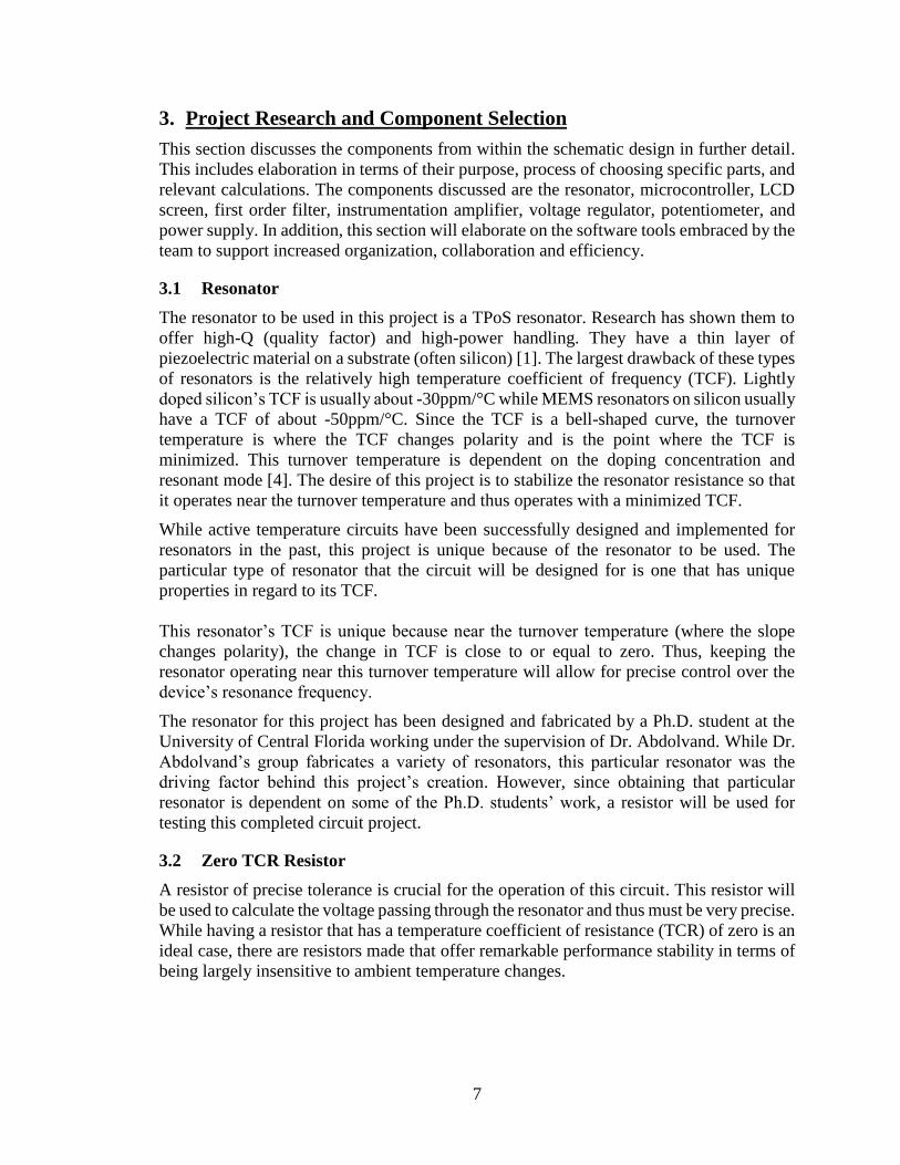
computer (RISC) architecture that is composed of 16 registers. The function for each of
the 16 registers is shown in Figure 3-1.
Figure 3-1: Register functions for the MSP430’s CPU [5]
3.3.1 Communication Interface
Wired communications are used to establish connection between hardware components in
a given system. For example, wired communication is utilized for the data transfer between
a microcontroller and an LCD. The types of communications between digital devices can
be categorized as either parallel communication or serial communication. Parallel
communication requires the transmission medium to have independent signal lines
corresponding to the number of transmitted digital word bits. This allows all the bits of one
word to be transmitted simultaneously and at a high rate. On the other hand, serial
communication requires only one signal line as the bits are received in a sequence. The
transmission rate for serial communication is low. The options for each communication
type is discussed below.

11
3.3.1.1 Serial Communication
The process of transmitting data one bit at a time in sequential order over a communication
channel is referred to as serial communication. There are different options for standardized
serial communication technologies including I2C, SPI and UART. The former two are
characterized as synchronous serial communication processes. These methods are
potentially advantageous for interfacing the microcontroller to hardware subsystems. The
latter is an asynchronous process that can be beneficial for sending and receiving data
between external devices. For this application, synchronous processes would be
appropriate as the LCD is considered to be a subsystem.
The Inter-Integrated Circuit (I2C) is a serial communication protocol that utilizes a serial
bus to advance communication between devices so that multiple masters are able to
interface with multiple slaves. The method is purposed for short distance applications
especially communication between integrated circuits within a common PCB. Further, it is
often used at low speeds. An I2C bus uses a 7-bit addressing scheme and two signals: Serial
Data (SDA) and Serial Clock (SCL). The former is the data signal that transmits data
bidirectionally between masters and slaves at the pace of the clock signal which is able to
be controlled by the master or slave. The signals are transmitted using designated encoded
messages and the desired slave’s 7-bit address. Unlike SPI and UART, the I2C signal bus
lines are open-drain and maintain low signals so I2C is an active-low method. I2C is a
relatively popular and robust method of serial communication and is supported by many
devices.
The Serial Peripheral Interface (SPI) is a serial communication method also intended for
small distance usage and characterized by its simplicity and multipurpose quality. It is
considered to be a standard method of serial communication for embedded systems
especially for LCD screens. Similar to I2C, SPI implements the master and slave process.
However, instead of two signals, it contains four: Slave Select (SS), Serial Clock (SCLK),
Master In Slave Out (MISO) and Master Out Slave In (MOSI). The SPI method supports
a single master and multiple slaves. The full-duplex design of SPI makes a more simple
and faster alternative to I2C. However, it requires more signal wires and slaves are not able
to communicate with each other.
3.3.1.2 Parallel Communication
The process of transmitting data multiple bits at a time in parallel over a communication
channel is referred to as parallel communication. Parallel communication can serve as a
faster interface between digital devices provided noise issues do not arise. This
communication is appropriate when speed rather than space is more important. The
disadvantages with regard to parallel communication surface when communication is
needed across a long distance. However, this is not an issue for this application. Parallel
mode can be implemented in 4-bit or 8-bit mode. The 8-bit mode is more efficient as a data
byte can be transmitted to the display in one cycle while the 4-bit mode transmits the single
bit in two 4-bit nibbles. This saves pins of the microcontroller but takes the transmission
take twice as long.
3.3.1.3 Communication Interface Selection

12
In summary, the microcontroller must have at least one communication interface to
transmit data to the LCD. The types of serial communications frequently used in
combination with microcontrollers include serial peripheral interfaces (SPI), inter-
integrated circuit buses (I2C), and asynchronous serial communication. The former two are
often used to exchange data between a microcontroller and other devices on the same PCB
while the latter communicates with devices such as a PC. SPI and I2C can be used to
communicate with ADCs and DACs, sensors with digital output and other processors.
Although SPI and I2C comparable applications, the latter is a true bus devised to
accommodate many devices and supports half-duplex transmission. On the other hand, SPI
uses two lines for data transmission and data can be sent in either direction at the same
time. SPI uses more wires and offers a simple and fast interface.
Parallel communication is also a viable option considering the flexibility and ease of
connection. The parallel method does not require use of a shift register and requires either
four or eight bits for the data lines. The parallel communication methods are often quicker
than the serial communication methods while is important since the LCD will need to be
constantly refreshed to update the resistance measurement to the user.
For this application, the parallel communication will be used to interface the LCD to the
microcontroller. The LCD can receive data by configuring the hardware connections to the
microcontroller and defining the bits appropriately within the program. This will be
achieved through initialization of the LCD screen and transmission of the data periodically
to display the updated variables when the screen is refreshed. The resistance and current
values will be passed as strings from the microcontroller to the LCD.
3.3.2 Accuracy
The objective for this project is to stabilize the resistance of resonator to achieve peak
performance. Thus, there is an emphasis on accuracy rather than speed with regard to this
application to ensure that high precision is executed. The selected microcontroller needs to
have an appropriate ADC range and offer performance stability after each use.
3.3.3 MSP430 Series
The microcontroller families under consideration for this application were the Texas
Instruments MSP430 and MSP432, the Microchip PIC24F, and the Silicon Labs Gecko.
The Texas Instruments MSP430 family of microcontrollers offers an extensive variety of
low-power consumption and integrated analog and digital devices designed for sensing and
measurement applications. The MSP430 employs a 16-bit RISC CPU, 16-bit registers and
constant generators that allow for efficient code implementation. Furthermore, its
configurable features enable it to be a practical solution for many low-power applications.
The MSP430 offers many series of this product that can be selected in terms of hardware
interfaces, architecture, and memory specific to this project.
The advantages to this microcontroller include its low cost, online community support and
familiarity in terms of language and Integrated Development Environment (IDE) due to its
presence in the curriculum. On the other hand, the disadvantages include the programming
intricacies associated with integrating an LCD and reading in analog inputs.
3.3.4 MSP432 Series

13
The Texas Instruments MSP432 microcontroller family offers a wide variety of low-power
operation devices intended for high-performance applications. The MSP430 employs a 32-
bit ARM Cortex-M4F processor, integrated precision ADC, and pin-to-pin scalability that
allows for scalable code implementation. Further, its configurable features enable it to be
an adaptable solution for many low-power applications. Similar to the MSP320, the
MSP432 offers various series of this product that can be selected specific to this project.
3.3.5 PIC24F Series
The Microchip PIC24F microcontroller family presents a cost-effective, low-power and
high-performance solution to embedded applications. The PIC24F features potential for
precision time measurement, capacitive touch implementation and an integrated graphical
or segmented display. In addition, it captures rich analog integration and serial
communications that are necessary for this project. The broad product line ranges from
low-power microcontrollers to high performance dual-core digital signal microcontrollers.
The advantages to this microcontroller include its ability to be incorporated with customer
applications and provide low-cost and reduced time solutions. In addition, there is an
emphasis on precision time measurement and the integration of displays. The
disadvantages include its nonconfigurable complex features that are not necessary for this
application.
3.3.6 Gecko Series
The Silicon Labs Gecko microcontroller family is designed for battery-operated
applications and high performance and low-power systems. The Gecko is a 32-bit
microcontroller that is based on the ARM Cortex-M3 core and offers an extensive variety
of low-power and efficient devices designed for response and power-sensitive applications.
The Gecko family offers many series of this product with specifications that can be
configured specific to this project.
The advantages to this microcontroller include its mathematical capabilities, digital and
analog peripherals and configurable LCD controller. The disadvantages include its other
unnecessary features and the lack of background and community with this type of
microcontroller.
3.3.7 Series Selection
The specifications and characteristics for the microcontrollers detailed above are shown in
Table 3-2 in a more readable format.
14
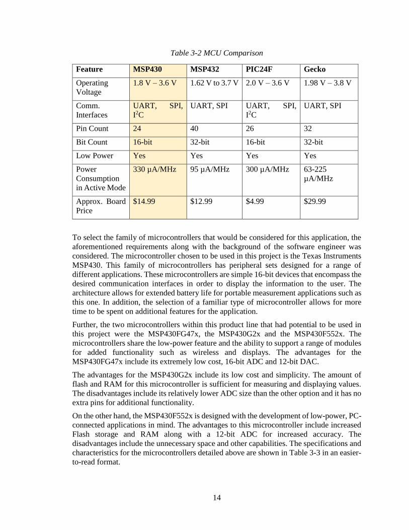
Table 3-2 MCU Comparison
Feature MSP430 MSP432 PIC24F Gecko
Operating
Voltage
1.8 V – 3.6 V 1.62 V to 3.7 V 2.0 V – 3.6 V 1.98 V – 3.8 V
Comm.
Interfaces
UART, SPI,
I2C
UART, SPI UART, SPI,
I2C
UART, SPI
Pin Count 24 40 26 32
Bit Count 16-bit 32-bit 16-bit 32-bit
Low Power Yes Yes Yes Yes
Power
Consumption
in Active Mode
330 µA/MHz 95 µA/MHz 300 µA/MHz 63-225
µA/MHz
Approx. Board
Price
$14.99 $12.99 $4.99 $29.99
To select the family of microcontrollers that would be considered for this application, the
aforementioned requirements along with the background of the software engineer was
considered. The microcontroller chosen to be used in this project is the Texas Instruments
MSP430. This family of microcontrollers has peripheral sets designed for a range of
different applications. These microcontrollers are simple 16-bit devices that encompass the
desired communication interfaces in order to display the information to the user. The
architecture allows for extended battery life for portable measurement applications such as
this one. In addition, the selection of a familiar type of microcontroller allows for more
time to be spent on additional features for the application.
Further, the two microcontrollers within this product line that had potential to be used in
this project were the MSP430FG47x, the MSP430G2x and the MSP430F552x. The
microcontrollers share the low-power feature and the ability to support a range of modules
for added functionality such as wireless and displays. The advantages for the
MSP430FG47x include its extremely low cost, 16-bit ADC and 12-bit DAC.
The advantages for the MSP430G2x include its low cost and simplicity. The amount of
flash and RAM for this microcontroller is sufficient for measuring and displaying values.
The disadvantages include its relatively lower ADC size than the other option and it has no
extra pins for additional functionality.
On the other hand, the MSP430F552x is designed with the development of low-power, PC-
connected applications in mind. The advantages to this microcontroller include increased
Flash storage and RAM along with a 12-bit ADC for increased accuracy. The
disadvantages include the unnecessary space and other capabilities. The specifications and
characteristics for the microcontrollers detailed above are shown in Table 3-3 in an easier-
to-read format.
15
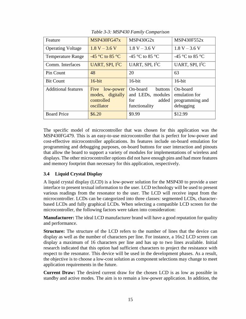
Table 3-3: MSP430 Family Comparison
Feature MSP430FG47x MSP430G2x MSP430F552x
Operating Voltage 1.8 V – 3.6 V 1.8 V – 3.6 V 1.8 V – 3.6 V
Temperature Range -45 °C to 85 °C -45 °C to 85 °C -45 °C to 85 °C
Comm. Interfaces UART, SPI, I2C UART, SPI, I2C UART, SPI, I2C
Pin Count 48 20 63
Bit Count 16-bit 16-bit 16-bit
Additional features Five low-power
modes, digitally
controlled
oscillator
On-board buttons
and LEDs, modules
for added
functionality
On-board
emulation for
programming and
debugging
Board Price $6.20 $9.99 $12.99
The specific model of microcontroller that was chosen for this application was the
MSP430FG479. This is an easy-to-use microcontroller that is perfect for low-power and
cost-effective microcontroller applications. Its features include on-board emulation for
programming and debugging purposes, on-board buttons for user interaction and pinouts
that allow the board to support a variety of modules for implementations of wireless and
displays. The other microcontroller options did not have enough pins and had more features
and memory footprint than necessary for this application, respectively.
3.4 Liquid Crystal Display
A liquid crystal display (LCD) is a low-power solution for the MSP430 to provide a user
interface to present textual information to the user. LCD technology will be used to present
various readings from the resonator to the user. The LCD will receive input from the
microcontroller. LCDs can be categorized into three classes: segmented LCDs, character-
based LCDs and fully graphical LCDs. When selecting a compatible LCD screen for the
microcontroller, the following factors were taken into consideration:
Manufacturer: The ideal LCD manufacturer brand will have a good reputation for quality
and performance.
Structure: The structure of the LCD refers to the number of lines that the device can
display as well as the number of characters per line. For instance, a 16x2 LCD screen can
display a maximum of 16 characters per line and has up to two lines available. Initial
research indicated that this option had sufficient characters to project the resistance with
respect to the resonator. This device will be used in the development phases. As a result,
the objective is to choose a low-cost solution as component selections may change to meet
application requirements in the future.
Current Draw: The desired current draw for the chosen LCD is as low as possible in
standby and active modes. The aim is to remain a low-power application. In addition, the

16
selection of a low-current device will enhance the battery life and the allocation of power
to other resources.
Power: The selected LCD is required to run off of 5V in order to maintain the low-power
quality of the application.
Interface: The LCD interface to the microcontroller is required to have compatibility with
the MSP430FG479.
Cost: The objective is to find the most cost-effective device that meets the given
requirements since the project is in the prototyping phase. The selected LCD screen will
preferably be simple and not have unnecessary features.
The options for the LCD screen were narrowed to the Lumex LCM-H01604DSF,
Electronic Assembly EA 8081-A3N, TinSharp TC1602A-09T, Microtips Technology
NMTC-S20200BMNHSGW-12, Gravitech LCD-20x4Y and Newhaven Display NHD-
0216K1Z-FL-YBW.
3.4.1 Choosing Series for Comparison
The following table describes six different LCD screens that were selected for part
comparison. To make the optimal selection, research was done for each component to
assess its potential benefits and detriments.
On the website of Mouser (an electronic parts distributer), LCD screens were searched for
and then filtered for LCD Character Display Modules.

17
Table 3-4: Comparison of LCDs
Product Manufacturer Driver
Voltage
Character
Arrangement
Number
of pins
Display Type Price
LCM-
H01604
DSF
Lumex 5V 16x4 16 STN,
Transflective
$27.92
EA
8081-
A3N
Electronic
Assembly
5V 8x2 14 Neutral, Blu-
Contrast, STN,
Reflective
$16.97
TC1602
A-09T
TinSharp 5V 16x2 16 STN,
Transmissive,
Negative, Blue
$9.95
NMTC-
S20200
BMNH
SGW-
12
Microtips
Technology
4.5V 20x2 16 STN,
Transmissive,
Negative
$15.74
LCD-
20x4Y
Gravitech 4.7V 20x4 16 STN yellow
green
$14.35
NHD-
0216K1
Z-FL-
YBW
Newhaven
Display
5V 16x2 16 STN yellow
green,
Transflective
$10.50
There are couple of different types of LCD screens that should be defined before the parts
are looked at more closely. A STN (super twisted neumatic) display has a 180°-270° light
twist and uses birefringence to absorb and pass particular wavelengths. The “twisted”
component of the name refers to the rotation of molecules from one plane to another). An
STN LCD screen is a type of passive display, and its display is usually monochromatic.
Transistors in a passive display usually activate an entire row or column rather than an
individual pixel like an active display. Negative and neutral refer to the type of lighting
contrast used between the characters and the background of the LCD.
Transmissive displays have a backlight that make the screen very readable indoors but can
be hard to read in direct sunlight. Reflective displays have a mirror layer that provides the
back light by reflecting the ambient light. However, it usually has lower resolution that
makes it difficult to read in dim lighting. Transflective displays can both reflect and
transmit light. This means that it generally uses a backlight in ambient indoor lighting as
the primary backlight, but outdoors, it can reflect light, so that becomes the primary
backlight source. This compromise of using both transmission and reflection also means
that the display is typically dimmer in all lighting conditions [6].

18
The driver voltage is a measure of drain voltage. Since LCDs are transistor based (typically
using field effect transistors), this is a measure of voltage at the drain of the FETs. This
voltage is the minimum amount of voltage that must be applied to the transistor to turn on
the LCD and thus can be considered the positive power requirement. If the LCD has too
low of a driver voltage applied to it, the characters may seem too dimly lit, and if the driver
voltage is too high, then segments that are off may also appear to be partially on.
The LCD screens compared here have an arrangement of the characters in a manner that
resembles the following figure, with the number in the above table represented as AxB,
where ‘A’ is the number of characters per row, and ‘B’ is the number of rows on the LCD.
Figure 3-2: LCD arrangement of characters
Sometimes, the LCD screens need a separate controller to operate, although some LCD
screens contain a controller. The controller has a clock, registers, voltage waveforms, and
bias voltages that control the operation of the LCD per user programming. Some LCD
controllers also need to be used in conjunction with a microcontroller.
3.4.2 LCM-H01604DSF
This LCD screen offers a 62 mm x 25.6 mm viewing screen with characters 4.75 mm x
2.95 mm. It is available in bulk packages and is RoHS compliant [7]. Out of the options
brought into consideration for the project, it is one of only two options with a transflective
display and the only one that can display 64 characters, which is the second highest number
of characters of the options inspected here. However, it also has the most expensive price.
3.4.3 EA 8081-A3N
This LCD screen offers a package size of 40 mm x 20 mm with a letter height of 5.11mm
and is interfaced via an 8-bit data bus [8]. It includes a controller, the ST7066. It is available
in bulk packages and is RoHS compliant. Out of the options brought into consideration for
the project, it is the only option with an 8x2 character display and the only one that can
display 16 characters, which is the lowest number of characters of the options inspected
here. However, it also has the second most expensive price.

19
3.4.4 TC1602A-09T
This LCD screen can be interfaced with a controller and is interfaced via a 4 or 8-bit parallel
data bus [9]. It is available in COB (Chip on Board) packages and is RoHS compliant. Out
of the options brought into consideration for the project, it is one of only two options with
an 16x2 character display, which is just beneath the average number of characters of the
options inspected here. However, it also has the least expensive price.
3.4.5 NMTC-S20200BMNHSGW-12
This LCD screen offers a viewing area of 82.2 mm x 18.2 mm and is interfaced via a 4-bit
data bus [10]. It is available in bulk packages and is RoHS compliant. Out of the options
brought into consideration for the project, it is the only option with an 20x2 character
display and the only one that can display 40 characters. It also has the lowest driver voltage
and a price point in the middle of the options.
3.4.6 LCD-20x4Y
This LCD screen offers a viewing area of 76 mm x 25.2 mm and can be interfaced with a
controller and is interfaced via a 4 or 8-bit parallel data bus [11]. It is available in bulk
packages and is RoHS compliant. Out of the options brought into consideration for the
project, it is one of only two options with a 20x4 character display and the only one that
can display 80 characters, which is the highest number of characters of the options
inspected here. It also has a price point in the middle of the options.
3.4.7 NHD-0216K1Z-FL-YBW
This LCD screen offers a package size of 80 mm x 36 mm and is interfaced via an 8-bit
data bus [12]. It contains a built-in controller, the ST7066. It is available in bulk packages
and is RoHS compliant. Out of the options brought into consideration for the project, it is
one of only two options with an 16x2 character display, which is just beneath the average
number of characters of the options inspected here. It also has the second lowest price out
of all the options.
3.4.8 Series Selection
In this project, the purpose of the LCD is to display the resistance readings. Since this
information would ideally include numerical and alphabetical characters and symbols, the
most appropriate type of display would be the character-based LCD. The compatible
display selected to present the measurement readings is a 16x2 character-based LCD
interface card. This will allow flexibility in displaying one measurement at a time with
toggling functionality or both measurements simultaneously on the LCD in an easy-to-read
format.
To select a 16x2 bit interface card, the communication interface, number of general I/O
pins and cost were considered. As mentioned above, the desired communication interface
to be used is the serial peripheral interface (SPI). The desired number of I/O pins necessary
is approximately ten pins. Lastly, the ideal cost would be less than $20 for this display.
After thorough consideration, the specific model display chosen is the TC1602A-09T. This
LCD is relatively inexpensive as it remains below half of the allotted budget for this part.
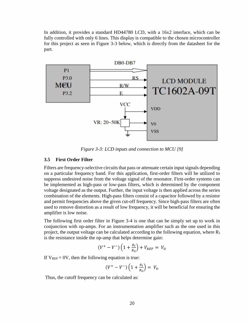
20
In addition, it provides a standard HD44780 LCD, with a 16x2 interface, which can be
fully controlled with only 6 lines. This display is compatible to the chosen microcontroller
for this project as seen in Figure 3-3 below, which is directly from the datasheet for the
part.
Figure 3-3: LCD inputs and connection to MCU [9]
3.5 First Order Filter
Filters are frequency-selective circuits that pass or attenuate certain input signals depending
on a particular frequency band. For this application, first-order filters will be utilized to
suppress undesired noise from the voltage signal of the resonator. First-order systems can
be implemented as high-pass or low-pass filters, which is determined by the component
voltage designated as the output. Further, the input voltage is then applied across the series
combination of the elements. High-pass filters consist of a capacitor followed by a resistor
and permit frequencies above the given cut-off frequency. Since high-pass filters are often
used to remove distortion as a result of low frequency, it will be beneficial for ensuring the
amplifier is low noise.
The following first order filter in Figure 3-4 is one that can be simply set up to work in
conjunction with op-amps. For an instrumentation amplifier such as the one used in this
project, the output voltage can be calculated according to the following equation, where RI
is the resistance inside the op-amp that helps determine gain:
(𝑉+ − 𝑉−) (1 +𝑅𝐼
𝑅𝐺) + 𝑉𝑅𝐸𝐹 = 𝑉𝑂
If VREF = 0V, then the following equation is true:
(𝑉+ − 𝑉−) (1 +𝑅𝐼
𝑅𝐺) = 𝑉𝑂
Thus, the cutoff frequency can be calculated as:

21
𝑓𝑐𝑢𝑡𝑜𝑓𝑓 = 1
2𝜋(𝑅1 + 𝑅2)𝐶
The capacitor for the filter will be ceramic, as this offers a low losses and high stability,
which is especially useful for this application involving resonators. The following image
depicts a first order filter as will be used for this project on the instrumentation amplifiers
to filter noise from the circuit.
Figure 3-4: First order filter
3.6 Instrumentation Amplifiers
Instrumentation amplifiers use three op-amps to measure the voltage difference between
the inputs. A sample of the inside of an instrumentation amplifier is shown below.
Figure 3-5: Sample instrumentation amplifier
In Figure 3-5, Rg determines the gain such that the following equation represents the
behavior of the sample instrumentation amplifier:
𝑉𝑜 = (1 +2𝑅
𝑅𝑔)(𝑉𝑖𝑛+ − 𝑉𝑖𝑛−)
Each instrumentation amplifier contains a setup similar to Figure 3-5, although they all
have varying gain equations that are determined by the resistors inside of the package.

22
Many instrumentation amplifiers are also rated for single supply operation and thus have a
voltage reference terminal to shift the range of operation.
Instrumentation amplifiers boast a higher input impedance and thus a lower input bias
current than a differential amplifier. For a precision application such as this one, an
instrumentation amplifier is a suitable choice. There are a variety of instrumentation
amplifiers available in integrated circuit packages that will help fulfill the accuracy
requirements for this project.
The output voltage can be calculated according to the following equation:
(𝑉+ − 𝑉−) (1 +𝑅𝐼
𝑅𝐺) + 𝑉𝑅𝐸𝐹 = 𝑉𝑂
The inputs to the positive and negative terminals are V+ and V-, RI is the internal resistance
that is used to set the gain (shown above as 2R), and VREF is the reference voltage. There
are a few requirements from the datasheet that should be noted and obeyed: the reference
input must be a low impedance connection. Even a few Ohms can degrade the performance
of the instrumentation amplifier. Furthermore, 0.1µF tantalum bypass capacitors should be
added in parallel to the power supplies to reduce noise.
3.6.1 Choosing Series for Comparison
Choosing an instrumentation amplifier involved visiting the websites of different
manufacturers and distributers. For parts from Renesas, the website of Mouser, an
electronic component distributer, was visited. Then, single channel precision
instrumentation amplifiers were investigated. One with zero drift was chosen for closer
comparison.
Analog Devices’ website was searched for instrumentation amplifiers, and then the single
channel products were considered. Options with precision or low noise were then located
and selected for final consideration.
On Texas Instrument’s website, options for instrumentation amplifiers include low noise,
low power, low offset, and high voltage. Since precision is the main concern for this
project, the low noise series was selected. From there, the search was narrowed to
amplifiers with only one channel, since each instrumentation amplifier did not need to have
more than one set of V+ and V- inputs. Three products were then selected from this list for
comparison. A table comparing all of the inspected products has been created below, and
the following sections describe some of the features of each type of instrumentation
amplifier.
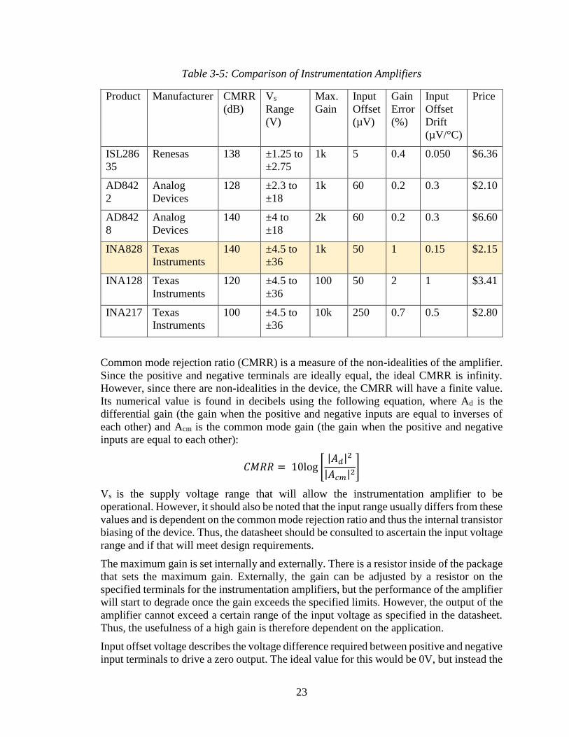
23
Table 3-5: Comparison of Instrumentation Amplifiers
Product Manufacturer CMRR
(dB)
Vs
Range
(V)
Max.
Gain
Input
Offset
(µV)
Gain
Error
(%)
Input
Offset
Drift
(µV/°C)
Price
ISL286
35
Renesas 138 ±1.25 to
±2.75
1k 5 0.4 0.050 $6.36
AD842
2
Analog
Devices
128 ±2.3 to
±18
1k 60 0.2 0.3 $2.10
AD842
8
Analog
Devices
140 ±4 to
±18
2k 60 0.2 0.3 $6.60
INA828 Texas
Instruments
140 ±4.5 to
±36
1k 50 1 0.15 $2.15
INA128 Texas
Instruments
120 ±4.5 to
±36
100 50 2 1 $3.41
INA217 Texas
Instruments
100 ±4.5 to
±36
10k 250 0.7 0.5 $2.80
Common mode rejection ratio (CMRR) is a measure of the non-idealities of the amplifier.
Since the positive and negative terminals are ideally equal, the ideal CMRR is infinity.
However, since there are non-idealities in the device, the CMRR will have a finite value.
Its numerical value is found in decibels using the following equation, where Ad is the
differential gain (the gain when the positive and negative inputs are equal to inverses of
each other) and Acm is the common mode gain (the gain when the positive and negative
inputs are equal to each other):
𝐶𝑀𝑅𝑅 = 10log [|𝐴𝑑|2
|𝐴𝑐𝑚|2]
Vs is the supply voltage range that will allow the instrumentation amplifier to be
operational. However, it should also be noted that the input range usually differs from these
values and is dependent on the common mode rejection ratio and thus the internal transistor
biasing of the device. Thus, the datasheet should be consulted to ascertain the input voltage
range and if that will meet design requirements.
The maximum gain is set internally and externally. There is a resistor inside of the package
that sets the maximum gain. Externally, the gain can be adjusted by a resistor on the
specified terminals for the instrumentation amplifiers, but the performance of the amplifier
will start to degrade once the gain exceeds the specified limits. However, the output of the
amplifier cannot exceed a certain range of the input voltage as specified in the datasheet.
Thus, the usefulness of a high gain is therefore dependent on the application.
Input offset voltage describes the voltage difference required between positive and negative
input terminals to drive a zero output. The ideal value for this would be 0V, but instead the

24
input offset voltage has a nonzero voltage because there will always be a slight mismatch
between the terminals since ideal cases are unrealistic. The lower the input offset voltage
is, the better.
The gain error refers to the expected closed loop gain versus the actual closed loop gain
and relates back to the open-loop gain. Essentially, the value for the closed loop gain is
calculated using the feedback ratio, β, using the following equation:
𝐴𝐶𝐿 =1
1𝐴𝑂𝐿
+ 𝛽
The ideal value of the open loop gain (AOL) is infinity, but, it actually has a finite number
associated with it that changes with frequency. Thus, there will be some error between the
ideal and actual closed loop gain. Lower the percentage error between these two is better.
The input offset drift is a measure of how much the input offset voltage will change with
temperature. The higher the input offset drift, the more sensitive the input offset voltage is
to changes in surrounding temperature. Thus, a lower value for input offset drift is
desirable.
3.6.2 ISL28635
This instrumentation amplifier has a programmable gain and offers rail-to-rail output. It is
available in packages of 14-lead Thin Shrink Small Outline Packages (TSSOP). Its
recommended uses are for sensing applications. Out of the options brought into
consideration for the project, this one has the lowest input offset voltage and input offset
drift and the second highest CMRR. However, it has the most limited supply voltage range
and second most expensive price [13].
3.6.3 AD8422
This instrumentation amplifier also has a programmable gain and allows for outputs within
±0.2V of the supply voltages. It is available in packages of 8-lead (Micro Small Outline
Packages) MSOP and Small Outline Integrated Packages (SOIC). Suggested applications
include data acquisition, process controls, and transducer communications. This device has
the lowest gain offset, second lowest input offset drift, and lowest price out of the ones
compared here. However, its maximum gain is only 1000 [14].
3.6.4 AD8428
This instrumentation amplifier has a fixed gain and offers rail-to-rail output. It is available
in packages of 8-lead (Micro Small Outline Packages) MSOP and Small Outline Integrated
Packages (SOIC). Its recommended uses include sensing applications and monitoring for
medical applications. Out of the options investigated for this project, it has the lowest gain
error and highest CMRR, but also the most expensive price [15].
3.6.5 INA828
This instrumentation amplifier has a programmable gain of up to 1000 and output within
±0.15V of the supply voltages. This provides a wide operating range for the device. It is
25
available in a package of 8-lead Small Outline Integrated Packages (SOIC). Its
recommended uses include process controls, medical applications, and circuit breakers.
Out of the options investigated for this project, it has the second lowest input offset drift
and highest CMRR but also the second highest gain error [16].
3.6.6 INA128
This instrumentation amplifier has a programmable gain of up to 1000 and output within
±0.9V of the supply voltages. This provides a good operating range for the device, although
it is not as wide as some of the other options. It is available in a package of 8-lead Small
Outline Integrated Package (SOIC). Its recommended uses include amplifier circuits,
medical applications, and data acquisition. Out of the options investigated for this project,
it has the lowest gain but the second lowest CMRR and highest gain error and input offset
drift. Its price point sits in the middle of the others (which are under $3 or above $6) [17].
3.6.7 INA217
This instrumentation amplifier has a programmable gain of up to 10,000 and output within
±1.8V of the supply voltages. This provides a good operating range for the device, although
that is the most restrictive limit on the output voltage of the parts compared here. It is
available in a package of 16-lead Small Outline Integrated Package (SOIC) or 8-lead Dual
In-line Package (DIP). Its recommended uses include microphone preamplification,
receivers, and amplifier circuits. Out of the options investigated for this project, it has the
highest gain but the lowest CMRR, highest input offset voltage, and second highest input
offset drift. Its price point sits closer to the middle but is on the lower end of the prices
compared here [18].
3.6.8 Final Selection
The instrumentation amplifier chosen for this project was the INA828. It is a low noise,
low power instrumentation amplifier that requires a supply voltage of ±4.5V to ±18V. The
target supply voltage for this circuit is ±10V; thus, the INA828 is a suitable choice. The
input voltage can range from V- + 2V to V+ - 2V before the performance will start to
degrade. This instrumentation amplifier also offers the highest CMRR and has a reasonable
price point.
3.6.9 Measure Voltage Across Resonator
To measure the voltage across the resonator, an instrumentation amplifier will be used.
There should not be any gain on the input signal as the exact value is desired to be passed
into the microcontroller. Thus, the voltage measured across the resonator should equal:
Rres*Ires = Vres
Ires will be set by the voltage input and controlled by the microcontroller. However, before
Vres is passed into the microcontroller, it will need to be scaled so that it does not exceed
the maximum 3.6V allowed on the microcontroller pins.

26
3.6.10 Measure Voltage Across 10Ω Resistor
In a similar manner, the voltage passing through the 10Ω resistor will be equal to:
10Ω*Ires = V1kΩ
This value will also be passed into the microcontroller. Even though the current could also
be calculated using the initial VCCS, this will give a more accurate representation of what
the current is. The microcontroller should then calculate the resistance value of the
resonator using an equation similar to the following:
Vres*V10Ω
10Ω = Rres
This resistor must be very precise (with a TCR very close to zero) so that the voltage
measurement here will be accurate.
However, in order to optimize the resolution of the A/D conversion, the maximum voltage
measured across the resistor should equal the maximum voltage entering the
microcontroller, which is 3V. Should this be necessary, a gain can be implemented to meet
this condition. This could be done externally through a non-inverting amplifier circuit as
seen in section 6.5.7 or by adding a gain resistor to the INA828 operational amplifier.
The gain resistance value 𝑅𝐺 can be calculated using the equation from the INA828
datasheet [16]. By setting the gain equal to the desired gain, the equation can be solved for
the gain resistance value:
𝐺𝑎𝑖𝑛 = 1 +50𝑘Ω
𝑅𝐺
The gain resistance value 𝑅𝐺 is calculated to be 10kΩ. The gain resistor is then placed
between pin 1 and pin 8 of the INA828 instrumentational amplifier. The pin configuration
for this product is found within its datasheet and is shown in Figure 3-6 below [16].
Figure 3-6: INA828 pin configuration [16]
3.7 Voltage Regulator
The voltage regulator source will be used to provide a stable voltage for the proper biasing
of the transistor. A variety of different options were considered from different distributers
and manufacturers.

27
3.7.1 Choosing Series for Comparison
Choosing a voltage regulator involved visiting the websites of different manufacturers and
distributers. The website of Mouser, an electronic component distributer, was visited for
comparison of different options. Then, precision shunt voltage regulators and adjustable
precision shunt voltage regulators were examined closer, with a filter applied such that the
maximum output voltage of the regulator was at least 8V.
The search was then examined for voltage regulators that that were adjustable to a value
beyond 8V. Options from different manufacturers were inspected closer based on their
options and compatibility to other products.
An additional search was made on Texas Instrument’s website since comparing their
products on Mouser was more difficult that doing so on the company’s website. Options
for power management and then voltage regulators were selected. From there, the search
was narrowed to regulators with an 8.192V or higher option. Two products were then
selected from this list for comparison. A table comparing all of the inspected products has
been created below, and the following sections describe some of the features of each type
of voltage regulator.
Table 3-6: Comparison of Voltage Regulators
Product Manufacturer Output
Voltage
Range
Input
Voltage
Range
Input
Adjustment
Current
Max.
Output
Current
Price
LM317 Texas
Instruments
1.25V-
37V
3V-40V 50µA 1.5A $0.78
NCP110 ON
Semiconductor
-0.3V-
6V
-0.3V-
6V
20µA 300mA $0.37
MAX150
06
Maxim
Integrated
1.8V-
10V
4V-40V 10µA 350mA $1.33
TLS115
D0EJXU
MA1
Infineon
Technologies
-5V-
45V
4V-45V 30nA 150mA $1.45
NCP786
AMNAD
JTBG
ON
Semiconductor
-0.3V-
18V
-0.3V-
650V
150nA 11mA $0.85
TS31023 Semtech -0.3V-
18V
-0.3V-
18V
220µA 60mA $0.96
A voltage regulator is a circuit element that provides a certain voltage value for an
indefinite amount of time, with the two main groups being linear regulators and switching
regulators. Linear regulators usually have two (or three if the regulator is adjustable)
28
terminals, and most use power BJTs or MOSFETs to act as a variable resistor internally.
They come in small packages and usually work over a range of currents and loads but are
generally inefficient because of the conversion of unused energy into heat. There are two
types of linear regulators.
Series regulators typically use a Zener diode in series with the power transistor to regulate
the current going to the power transistor. They are more efficient than shunt regulators, the
other type of linear regulators, because the Zener diode generates a small current at the
base of the transistor. Shunt regulators provide a path for the current to flow from the
supply voltage to the ground. The shunt regulator also uses a Zener diode to maintain a
constant voltage but not in a series arrangement. Thus, more energy is wasted with shunt
regulators than with series regulators.
Switching regulators use a controlled switch and turn on and off to generate the required
voltage. They are much more efficient than linear regulators due to the lower impedance
switch that sets the voltage. It feeds the unused energy back into the regulator and changes
the output little by little. Switching regulators, however, also tend to generate much more
noise than linear regulators because of the switching function.
A few of the characteristics of the regulators compared are described here. The output
voltage range describes the range of user-set output voltage values that the regulator can
handle, while the input voltage range describes the range of allowable input voltage values.
The adjustment (or quiescent) current describes the current that must pass through the
voltage regulator for the device to work. It must be greater than a certain minimum value
for the regulator to turn on but less than a specified maximum value to prevent the device
from having permanent damage. Often, the datasheet records an absolute maximum
adjustment current and recommended limit. Finally, the maximum output current describes
the highest current that the voltage regulator can generate.
3.7.2 LM317
This voltage regulator has an option to have the output voltage reach all the way to 37V. It
is available in packages of TO-92 (Transistor Outline Package, Case Style 220), SOT-223
(Small Outline Transistor), and TO-92 (Transistor Outline Package, Case Style 263) [19].
Its recommended uses include energy management, RFID reader, refrigerator, and more.
Out of the options brought into consideration for the project, this one has the second least
expensive price point and is about half of the price of the most expensive option. It also
has the highest input adjustment current and second highest maximum output current.
3.7.3 NCP110
The NCP110 adjustable voltage regulator was also selected for comparison. It is available
in packages of XDFN4 (Extremely Thin Dual Flat No Leads Package with 4 leads) or
WLCSP4 (Wafer Level Chip Scale Package with 4 leads). Its recommended uses include
battery-powered equipment, portable medical equipment, and smoke Detectors [20]. Out
of the options brought into consideration for the project, this one has the smallest range for
voltage input and output. With the project constraint of a 10V power supply, this voltage
regulator would need the power supply voltage stepped down before it could be safely
passed into the voltage regulator.
29
3.7.4 MAX15006
This voltage regulator source’s option has an adjustable input of up to 40V. It is available
in packages of TDFN (Thin Dual Flat No Leads packages) or SO (Small Outline packages),
which have six and eight pins, respectively. Its recommended areas of use include
automotive, telecom, tire-pressure monitoring, and more [21]. Out of the options brought
into consideration for the project, this one has the second highest price and an above
average maximum output current compared to the options compared here. The maximum
output voltage for this device is 10V, which is close to the desired value of 8.8V.
3.7.5 TLS115D0EJXUMA1
This voltage regulator source’s option does not have a built-in voltage regulator but instead
requires an external one. This device is available in packages of 8-Lead TSON (Small
Outline No Lead Package) or in packages of DSO-8 (Dual Small Outline Packages with 8
leads) [22]. Its recommended uses include automotive sensor supplies and precision
voltage replication, as well as high-precision voltage tracking. Out of the options brought
into consideration for the project, this one has the lowest input adjustment current and the
second largest input voltage range. However, it also has the highest price, and its need for
an external voltage regulator is undesirable.
3.7.6 NCP786AMNADJTBG
This voltage regulator has a built-in regulator of 1.275V ±3%. The output can be adjusted
up to 18V, allowing the user to determine the output voltage value. It is available in
packages of DFN (Dual-Flat No-Leads Package) and has six pins [23]. Its recommended
uses are for industrial applications, home appliances, and home metering. Out of the
options brought into consideration for the project, this one has the second lowest input
adjustment current. It also has the highest voltage input range by a significant margin and
an average price. However, the limit on the 11mA current output is hindering to the project
since a current greater than 11mA through the resonator (which is necessary to generate a
certain resistance) is no longer an option.
3.7.7 TS31023
This voltage regulator has a programmable value up to 18V, allowing the user to determine
the output voltage value. It is available in packages of DFN (Dual-Flat No-Leads Package)
and has eight pins. Its recommended uses include automotive and industrial applications,
as well as energy harvesting systems and wireless power [24]. Out of the options brought
into consideration for the project, this one has the highest input adjustment current and
second lowest maximum output current. However, the limit on the 60mA current output is
potentially hindering to the project since a current greater than 60mA through the resonator
(which may be necessary to generate a certain resistance) is no longer an option.
3.7.8 Final Selection
The voltage regulator to be used for this circuit is the LM317. This regulator was chosen
because of its ability to reach 8.8V or more and ability to offer a stable voltage at the lowest
price out to the options compared here. The LM317 offers the most flexibility in terms of
design since exact power supply voltages and currents still need to be tested.

30
Since the voltage supply will be 10V, the output voltage value must be less than that.
However, to have a certain range of current, the following equation must be satisfied:
IsetM(Rset + Rmea) + VresM + Vt = VregM
Vt is the turnon voltage of the transistor, and VresM is the maximum voltage across the
resonator (occurs when the current Iset is at its highest value(referred to here as IsetM) due
to Vi being at its highest value). Using estimated values from preliminary data, the
proposed value of VregM (the maximum voltage needed from the regulator source) is
estimated to be close to 8V. Thus, the LM317 regulator is a suitable choice for this circuit
since its output is adjustable up to 37V (limited to 10V by the power supply for this circuit).
Furthermore, the voltage regulator will be set up in a manner similar to the follow figure:
Figure 3-7: Sample voltage regulator set up
For this setup, the following equation must be satisfied:
𝑉𝑜𝑢𝑡 = 𝑉𝑟𝑒𝑔 (1 +𝑅2
𝑅1)
Vreg is given in the datasheet as 1.25V. For this circuit, a value of 8.8V is desired. Thus,
R2 = 6.04kΩ and R1 = 1kΩ is sufficient. Ceramic or tantalum bypass capacitors are also
recommended to help filter noise from the power supply. For this design, 0.1µF and 1µF
capacitors are used.
3.8 Potentiometer
A potentiometer (variable resistor) will be added to one of the power pins on the LCD for
contrast control of the screen. This potentiometer will need to be manually tuned. Hence,
the following sections detail different options for a manual potentiometer.

31
3.8.1 Choosing Series for Comparison
On the websites of Mouser and Digikey, both electronic component distributers,
potentiometers (variable resistors) were filtered so that rotary potentiometers were
displayed. A filter was then applied so that options with tolerances of 3% or less were
displayed. The following table provides an overview of the choices that will be compared.
Table 3-7: Comparison of Potentiometers
Product Manufacturer Linearity Tolerance Resistance
Range
Temperature
Coefficient
Price
P120P
K-
Y25BR
10K
TT
Electronics
±1% ±20% 1kΩ-10kΩ 50ppm/°C $0.59
3590S-
2-103L
Bourns ±0.25% ±5% 200Ω-
10kΩ
50ppm/°C $13.68
534B15
02JC
Vishay
Spectrol
±0.25% ±5% 100Ω-
100kΩ
20ppm/°C $16.18
RK09K
1130A8
G
ALPS ±5% ±30% 0Ω-10kΩ 100ppm/°C $0.57
3386P-
1-105
Bourns ±0.2% ±10% 10Ω-1MΩ 100ppm/°C $2.34
774-
284TB
CF504
A26A1
CTS
Electronic
Components
±2% ±10% 1kΩ-
500kΩ
100ppm/°C $12.61
There are many different types of potentiometers, many of which involve a mechanical
wiper moving along a resistive material. The wiper’s position determines the resistance
seen by the circuit. The most common type is a rotary potentiometer, where the wiper
moves along a circular path. All the potentiometers compared here are rotary with wipers
except for the 3386, which is a trimming potentiometer that requires a screwdriver to adjust
the resistance value.
Wirewound potentiometers essentially have a wire coiled inside of them that the wiper
slides along. The number of turns describes how many rotations it takes for the wiper to go
from its minimum to maximum position. Thus, more turns will allow for higher precision.
Linearity is the relationship between the position of the wiper or knob and the resistance
value. There are four types of linearity associated with potentiometers, but independent
linearity is what is described in the datasheet. It is the maximum allowable deviation
between any output value the corresponding linear value [25]. Thus, have a lower linearity
32
percentage value is better since it means that the output and expected value align more
closely.
The tolerance describes the percent error of the expected and actual resistance provided by
the potentiometer. Accuracy, especially for this application, is crucial. Thus, lower
tolerances are best. The resistance range describes what resistance values the potentiometer
can provide.
Here, temperature coefficient is used to predict the change in the expected resistance value
with respect to temperature changes. It is often a nonlinear value since it is the result of
idealities internal to the device. However, the temperature coefficient is a reliable estimate
about the device’s response to external temperature stimuli. Lower coefficients are better
for this value.
3.8.2 P120PK-Y25BR10K
This potentiometer has an adjustable resistance and can be tuned using a top-adjusted
mechanical shaft. It is available in panel mount packages. It has a life cycle of 100,000
turns and has an insulated shaft [26]. Out of the options brought into consideration for the
project, this one has the second highest tolerance and second lowest price. However, it has
a range of resistance that is average for the parts chosen.
3.8.3 3590S-2-103L
This potentiometer has an adjustable resistance and can be tuned using wipers. It is
available in bulk packages. It is made resistive using a wirewound 10 turn rotary metal
[27]. Out of the options brought into consideration for the project, this one has nearly the
tightest linearity and tolerance. However, it has a range of resistance that is average for the
parts chosen and a price point that is in the middle of the options.
3.8.4 534B1502JC
This potentiometer has an adjustable resistance and can be tuned using wipers. It is
available in bulk packages. It is made resistive using a wirewound 10 turn rotary metal
[28]. Out of the options brought into consideration for the project, this one has nearly the
tightest linearity and tolerance. However, it has a range of resistance that is average for the
parts chosen and a price point that is the highest out of the options compared here.
3.8.5 RK09K1130A8G
This potentiometer has an adjustable resistance and can be tuned using a physical shaft that
is 9.8mm tall. It is available in panel mount packages and has a life cycle of 10,000 turns
[29]. Out of the options brought into consideration for the project, this one has the highest
linearity and tolerance and average resistance range. However, it also has the lowest price
of the options.
3.8.6 3386P-1-105
This through hole potentiometer has a trimmable resistance and can be tuned a knob or slot
screwdriver. It is available in tape and reel, tube, and ammo packages. It has a single turn
that adjusts the resistance [30]. Out of the options brought into consideration for the project,

33
this one has the tightest linearity and but an averagely loose tolerance rating. However, it
has a range of resistance that is much higher than the other options, which helps balance
out the higher tolerance, and a price point that is lower than the median price of the options.
Trimming potentiometers have a much more limited lifespan (usually only about 200 turns)
than rotary potentiometers, which usually can support up to a million uses.
3.8.7 774-284TBCF504A26A1
This potentiometer has an adjustable resistance and can be tuned using wipers. It is
available in bulk packages. It is made resistive using a wirewound 1 turn rotary metal [31].
Out of the options brought into consideration for the project, this one has the second highest
linearity and tolerance and the narrowest resistance range. However, it also has a high
temperature coefficient and a medium price compared to the other options.
3.8.8 Final Selection
For this circuit, the RK09K1130A8G was chosen as the potentiometer. This option allows
for a long lifecycle and wide resistance range while keeping the price low and the device
small. For this project, the tolerance of the potentiometer was not crucial; thus, the higher
tolerance values were chosen over the more expensive but more precise potentiometers.
3.9 Switches
The switches used in this project are the SKQGADE010 by ALPS. Each one is connected
to a general purpose input/output (GPIO) pin on the microcontroller. However, because the
switches are mechanical, they tend to generate noise when being pressed that can interfere
with the microcontroller’s reading of them. Thus, a debouncing circuit was added around
each switch to debounce the switches using hardware.
The specifications for the SKQGADE010 state that it has a stabilization time of 15 ms,
meaning that 15 ms after the button has been pressed, it will reach a constant value and not
vacillate between its states (connected or not connected). Thus, the RC circuit associated
with the switch as a means of generating a delay will have a timing constant of 20 ms to
prevent issues with switch bouncing.
It also includes a pullup resistor so that the switch can have the proper voltage across it.
The following image depicts the switch debouncing circuit used in this design. RP is the
pullup resistor, RS and CS are the RC filter. The input voltage, in this case, comes from
the microcontroller.
Figure 3-8: Sample switch debouncing circuit

34
3.10 Power Supply
The main power supply will be used to provide the appropriate amount of voltage and
current to every part within the circuit. The best option for main power supply for this
application would be a bench power supply because they are very reliable, and the voltage
value can be changed easily in case it needs to be adjusted during part testing. To determine
the voltage needed for the main power supply, the voltage and current requirements for
every hardware component of the circuit must first be analyzed. The main power supply
must be greater or equal to the largest voltage needed within the circuit and will then be
stepped down to a lower voltage using several DC to DC conversion to obtain the needed
power for each component.
The Agilent E3631A triple output DC power supply will be used as the main power supply
and will be lent by the sponsor for testing and demonstration. It has three separate terminals
that can be used as DC voltage sources. The first terminal ranges from 0 to +6.18V, the
second terminal ranges from 0 to +25.75V, and the third terminal ranges from 0 to -25.75V
[32].
3.11 Software Tools
Team collaboration is essential to personal growth and delivering quality results, and there
are many tools that have been developed to overcome challenges that often arise within a
team environment. The tools utilized by this group are intended to foster effective team
collaboration and enhance productivity. The tools are purposed to facilitate scheduling,
tasking and organization while still maintaining the values of flexibility, responsibility and
professionalism. The software tools used by this team are categorized into communication,
development and documentation categories.
3.11.1 Communication
Effective communication is an integral skill for any type of team project. The use of
collaborative platforms for messaging, asking questions and sharing documents allows for
groups to remain on the same page during the development process. This team has chosen
to use Microsoft OneDrive and GitHub to enhance communication and collaboration.
3.11.1.1 Microsoft OneDrive
OneDrive is a cloud storage solution developed by Microsoft. It has been adopted as a
common place for sharing and storing documents used throughout the project lifecycle.
This software allows for the creation of shared folders that are stored in an online drive.
These folders are easily accessible from anywhere and are saved and updated in real-time
given there is a source of internet. The folder shared between members of this team is used
to store schematics and diagrams, documentation and relevant reading material.
In addition, OneDrive offers user-friendly and collaborative versions of Microsoft Office
documents which are helpful in managing the budget, parts and meeting notes. These files
created are then easily accessible and manageable within OneDrive. OneDrive is one of
the most popular cloud storage services offered for free for students. It is familiar to all
members of the team, so it is natural that this provider is utilized for sharing information.
35
3.11.1.2 CCS Cloud
CCS Cloud is a desktop IDE that allows for source code to be easily organized and shared
between team members. The projects are able to be developed and debugged online which
will allow the software component to be more portable. In addition, the files are able to be
stored remotely to the cloud which allows for ease of storing previous versions. These
projects are able to be imported from the cloud to the desktop version of Code Composer
Studio so that use of both IDEs simultaneously is a seamless process.
In addition, Texas Instruments provides this tool for free which will allow the project to
remain within budget while taking advantage of quality and cost-effective tools.
3.11.2 Development
The development of a project from its initial concept to prototyping to a deliverable product
is facilitated with the right tools. The integration of hardware and software components
into a common project requires a great deal of collaboration. Development tools can be
used to support debugging as well as design hardware components. The team has chosen
to use Autodesk Eagle and Code Composer Studio for hardware and software development,
respectively.
3.11.2.1 Integrated Development Environment
Code Composer Studio is an integrated development environment (IDE) that was designed
to support Texas Instruments’ family of microcontrollers and embedded processors. Code
Computer Studio provides a multitude of tools to develop and debug embedded
applications. In addition, it is comprised of a compiler, source code editor, debugger, and
project build environment. The tools and interfaces are user-friendly but also familiar to
the members of this team which makes it a perfect choice for our application. Essentially,
Code Composer Studio achieves the valuable aspects of Eclipse with advanced embedded
debug capabilities.
The choice of using a Texas Instruments microcontroller dictated the decision to adopt the
Code Composer Studio IDE. Code Composer Studio is a derivation of the Eclipse IDE that
integrates the advanced embedded debugging features from TI. It was created with the
purpose of supporting applications for TI microcontrollers and embedded processors, and
it includes a compiler designed for these embedded systems. In addition, it includes
libraries and community forums for further support of the devices. This was the only
software environment with compatibility with the selected microcontroller.
3.11.2.2 Programming Language
The languages available in Code Composer Studio are C, C++, and assembly. However,
the language of choice for these types of applications is often the C programming language
since C++ has limited support. C encompasses built-in and user-defined types, data
structures, and open control flow which make it the more productive and reliable language
with respect to assembly. High-level languages also often produce efficient code.
In addition, the architectures of modern processors are intended for compilers rather than
assembly code and online resources lean towards the C language approach. The software

36
lead, along with the rest of the team, is fluent in the C programming language. For these
reasons, the selected language for the project is C.
3.11.2.3 EAGLE
This project requires PCB design in order to implement specifically defined functionality
and features. It can be difficult to find a program that is within budget and competent for
the requirements of a project such as this one. Autodesk EAGLE is an electronic design
automation software purposed for PCB design. It allows PCB designers to easily integrate
schematic diagrams, components, and routing. Furthermore, it includes a user-friendly
schematic editor, a powerful set of PCB layout tools and a support community. Autodesk
provides a free three-year license for students.
3.11.3 Documentation
Documentation within a team can be challenging when the goal is to maintain consistent
formatting and a unified quality. The documentation was initially created within a Google
Doc for the sake of ease and real-time editing. However, with the preference for some of
the more complex features offered by Microsoft Word, the team made a decision early on
to transfer the documentation file to a shareable Microsoft Word document and use that
from that point forward.
3.11.3.1 Microsoft Word
Microsoft Word is a work processing software and document creator that contains various
tools for collaboration and editing. Microsoft Word contains development tools such as
automatic and dynamic table of contents and lists, spelling and grammar checking and track
changes which eliminates the overhead related to document organization and revisions. In
addition, documents are able to be saved in OneDrive and shared with others. The ability
to work together at the same time is integrated in Microsoft Office Online. Microsoft Word
Online allows for team members to create documents together in real-time.
37
4. Design Requirement Specifications, Constraints, and Standards
This section discusses design requirement specifications, constraints, and standards
relating to this project.
4.1 Design Requirement Specifications
Some design requirement specifications imposed by the project sponsor include a variety
of operational requirements that the final design must satisfy.
Table 4-1: Design Requirement Specifications
Description Value Related Standards/Purpose
Project Cost
Ceiling
$1000 No Related Standards. Low cost without limiting
project material quality. Designated by sponsor.
Time 31 Weeks (Total) No Related Standards. Time limitation of Senior
Design 1 and 2 courses to create, design, and build
a working prototype of project.
Accuracy Resistancestable at
setpoint ±1mΩ
No Related Standards. Required to ensure highest
accuracy which is a requirement set by sponsor.
Operating
Temperatures
Room temperature
(approximately 23
°C) to
greater than 85 °C
(approximately 90
°C)
Standard Industrial Limit is 85 °C (per MIL-STD-
810G). “Ensure the range of temperatures and rate
of change of the test item’s skin temperature is
adequate to achieve the test profile. A typical
range is -40°C to +85°C; “Necessary to go above
this standard value to test the effects of
temperature on resonance frequency.” [33]
Resonant
Frequency
70MHz with
minimal deviation
(+/ a few Hz)
No Related Standards. Specific to resonator used
within project which is set by sponsor.
4.1.1 Frequency
In the final design, the resonator should resonate around 70MHz. This is the resonance
frequency expected for the devices being fabricated by researchers in the Dynamic
Microsystems Lab at the University of Central Florida working under the supervision of
Dr. Abdolvand. By keeping the device operating at resonance frequency, the TCF can be
minimized and device performance optimized. 60-80 MHz is typical for the resonance
frequencies of these resonators; thus, 70MHz is the estimated value at which this device
should operate.
38
4.1.2 Resistance
To optimize frequency stability, the resistance needs to be kept constant. The chosen
method is to heat the circuit above industrial operating range and keep the resistance (and
thus temperature) stable there. Therefore, the resonator will need to operate above 85⁰C,
the limit of industrial operating range. The most critical part of this set point is the parts
per billion (ppb) accuracy desired.
4.1.3 Display
The design should incorporate a display to show operational resistance. This will allow the
user to know the resistance and verify the stability and accuracy of the control loop. There
will need to be a method of toggling cycling which one is displayed. This will need to be
connected to the microcontroller for calculations and functionality.
4.1.4 Modes of Operation
The design should incorporate a stand-by mode when the control loop is not active to save
power and demonstrate how the resonator operates without resistance control. In this stand-
by mode, the microcontroller will still measure and display the resistance but will not seek
to control the resistance. This contrasts with operational mode when the device is heated
to its desired resistance and kept there using a control loop.
4.1.5 Accuracy
The operation of the device should exhibit mΩ accuracy. This means that, when the
resonator has stabilized at the setpoint, it should deviate no more than ±1mΩ.
4.2 Design Constraints
Design constraints must be explored from different perspectives. These are conditions
imposed from outside sources that must be followed to have a successful design. This
section explores the economic, manufacturability and sustainability constraints, the social,
political and ethical constraints, and the environmental, health and safety considerations
for this project.
4.2.1 Economic, Manufacturability, and Sustainability
The economic constraint imposed for this project is to stay underneath of $500. This
includes all PCB design and components. Components are expected to consume less than
half of this budget. Thus, the main part of this budget will be taken up by the printing of
the PCB.
Manufacturing considerations must meet the needs of the PCB manufacturing. Routing and
grounding and traces must be laid out properly so that the circuit will be efficient and
function properly. Thickness of the PCB and number and layout of vias and pads must also
be considered for optimal creation of the board. Furthermore, the resonator is being
fabricated by Dr. Abdolvand’s research group; thus, the exact resonator to be used will be
dependent on project status of his students’ work.
Sustainability constraints related to the robustness of the design will be considered for this
project. First, the PCB must exhibit electrical sturdiness, such that it is able to handle the

39
input powers appropriately and not short circuit or exceed component limits easily. A
failsafe mode must also be created so that the resonator is protected from input voltage or
current errors. Additionally, good wire bonding practices should be followed so that the
circuit has stable connections and the resonator can be interchanged. The user should be
able to connect another resonator to the circuit and still have it function properly.
4.2.2 Social, Political, and Ethical
For this design, there are no social or political constraints that apply to this project. The
application for the product is limited since it is to be used as a method for members of the
Dynamic Microsystems Lab group to optimize performance of their devices and is not at
this time meant for wide-spread production.
The ethical constraints for this project relate to legal constraints as the device details of the
resonator may not be published yet and/or are proprietary. Thus, care should be taken to
use a resonator in the project but not disclose its operation or fabrication in detail.
4.2.3 Environmental, Health, and Safety
Environmental and health constraints should focus on using RoHS compliant parts. RoHS
(Restriction of Hazardous Substances) was first a 2003 European Union directive that
required heavy metals in products including lead and mercury to be replaced by safer
alternatives in future products. Since then, the directive has been expanded and adopted by
many countries globally [34]. RoHS parts are now readily available and used extensively.
Thus, parts that comply with RoHS regulations should be used here to maximize
environmental responsibility of the project.
To meet safety constraints, the circuit must be well grounded and offer stable power
connections. Both constraints are important for keeping the user safe from electric shock.
4.3 Standards
This section analyzes standards that are relevant to this project.
4.3.1 Safety Standards
IEC 60950-1:
This international standard will be referenced for its general principles of safety regarding
engineering design and operating equipment.
According to this standard, “Designers shall take into account not only normal operating
conditions of the equipment but also likely fault conditions, consequential faults,
foreseeable misuse and external influences such as temperature”. These principles will be
incorporated into the project design process in several ways. Datasheets for every
component are analyzed and considered during the design process, such as maximum and
minimum operating temperature, voltages, and current values [35].
This standard also discusses heat related hazards including “burns due to contact with hot
accessible parts” and due to “degradation of insulation and of safety-critical components”.
The standard offers suggestions on how to avoid these hazards including avoiding having
40
accessible high temperature components and providing markings to warn users when there
are high temperature parts accessible [35].
4.3.2 Testing Standards
MIL-STD-810G:
This military-grade standard will be referenced for its test method standards regarding
temperature and/or temperature change.
According to this standard, the typical industrial maximum product testing temperature is
85°C. The standard states to “Ensure the range of temperatures and rate of change of the
test item’s skin temperature is adequate to achieve the test profile”. A typical range is -
40°C to +85°C. However, to achieve the test profile of this specific resonance frequency,
it is important to go above this standard temperature value. The standard also states “the
rate of change may be as high as 4°C/min” which will be followed to ensure a slow
transition between each temperature so that the resonance frequency can stabilize [33].
4.3.3 Operating Standards
The circuit should be able to function as specified in the industrial operating range. A
primary advantage of this type of temperature control is that the circuit will not need to be
under vacuum but can be used in conditions of atmospheric pressure.
4.3.4 Software Standards
This section discusses standards that relate to software used for this project.
4.3.4.1 Standard SystemC Language Reference Manual Standard
The IEEE Std 1666-2011 is an IEEE standard used to define the SystemC library. SystemC
is described as “an ANSI standard C++ class library for system and hardware design for
use by designers and architects who need to address complex systems that are a hybrid
between hardware and software” [36]. In addition, this standard provides a comprehensive
SystemC class library definition such that the development of a SystemC application can
rely solely using this reference. As the complexity of the technology industry advances,
SystemC serves as a modeling language able to maintain these systems. Unlike traditional
hardware description languages, SystemC has the capability “for modeling hardware and
software together at multiple levels of abstraction” [36]. For this application, this standard
will prove beneficial for the software component of this project. The microcontroller will
implement the key functionality of the application using the C/C++ programming
languages, so this library will serve as an important reference.
4.3.4.2 Design Impact of Standard SystemC Language
This standard will allow for complex systems to be able to be properly addressed should
the opportunity arise. This project integrates software and hardware to achieve the specified
objectives, so this library should allow for more elaborate code to be written. The standard
will not inhibit the software design component of this project but serve as reference
containing recommendations for improved code usage.

41
4.3.4.3 Software Testing Standard
ISO/IEC/IEEE 29119 is a software testing standard intended for use for any software
development life cycle. The implementation of this standard will allow for “a high-quality
approach to testing that can be communicated throughout the world” [37] to be used for
the project. This standard serves as a reference to provide guidance regarding the proper
performance of testing processes and approaches as well as software documentation. For
this project, this standard will allow for the software component of this application to be
up to industry standards and thoroughly tested.
There are five distinct parts associated with this standard: concepts and definitions, test
processes, test documentation, test techniques and keyword-driven testing. The sections
that are applicable to this application are the second, third and fourth parts. These are
described in detail, with their relation to the project, below.
Part 2: Test Process
ISO/IEC/IEEE 29119-2 is a subsection of the software testing standard that delves into a
test process model that is able to be used in the software testing phase of any software
development cycle. Further, the standard elaborates on the software testing processes at the
organizational, test management and dynamic test levels. Testing is often used to mitigate
risk in software development; thus, the standard emphasizes “a risk-based approach to
testing” [37]. This standard will be beneficial to this project since this is a widely-used
approach to testing that prioritizes the most significant capabilities of the application.
The most applicable testing process for this application is the one at the organizational
level. Within the documentation, the standard elaborates on the procedures for the
development and evaluation of organizational test specifications and requirements. The
team of three students for this project serves as the “organization” for this test procedure.
The process of test management can be defined in terms of three individual phases: test
planning, test monitoring and test completion. Furthermore, existing test plans can be
implemented independently or as an integrated whole. It is important to note that phases
following this one follows the same structure regardless of the test plan implementation.
The actual testing stage will begin after the creation of a test plan. Test monitoring will
serve as a phase dedicated to address any issues that emerge during the testing. The test
plan should be modified to account for unexpected results should these types of issues
arise. The final test plan should ensure that organization test guidelines are met, and other
requirements are fully satisfied. The final stage, test completion, is comprised of test
processes regarding design and implementation, environment, performance and
documentation. The purpose of this stage is to ensure a comprehensive testing process and
addressment of the results.
Part 3: Test Documentation
ISO/IEC/IEEE 29119-3 is a subsection of the software testing standard that elaborates on
the appropriate methods of software testing documentation. The standard provides test
documentation examples that correspond to the process levels of the second part of the
standard. For the organizational test level, the standard defines the documentation for Test
Policy and Organization Test Strategy.

42
The Test Policy “defines the objectives and principles of software testing to be applied
within the organization” [37]. Further, it clarifies the goals to be achieved by testing, but it
does not delve into specifics regarding the testing procedure. The given template provides
a foundation for establishing and reviewing the organization’s policy. For this application,
this will allow for a comprehensible definition of the purpose of the testing to benefit all
members of the project.
The Organization Test Strategy serves as “a technical document that provides guidelines
on how testing should be carried out within the [project], i.e. how to achieve the objectives
stated in the Test Policy” [37]. In other words, this document should define the ‘how’ for
the ‘why’ defined in the template mentioned above. This template is generic and able to be
conformed to different types of projects. The implementation of this strategy will allow for
test sub-processes to be identified and defined. For this application, this portion of the
standard will allow for concise and complete organization regarding the proposed testing
procedure.
Part 4: Test Techniques
ISO/IEC/IEEE 29119-4 is a subsection of the software testing standard that defines various
software test design techniques that can be utilized during the phase described in the second
part of the standard. The techniques are described by three different test technique
categories: specification-based, structure-based and experience-based. For these test
techniques, the main source of information is what produces the expected results. Further,
the combined use of these different techniques can improve the effectiveness of the testing
procedure.
Specification-based test techniques use the test basis as the primary information source in
the design of test cases. Here, the test basis includes requirements and specifications,
models and user preferences. In addition, they emphasize the functional requirements of
the system. The standard describes many different techniques that are able to be used to
implement specification-based testing. It is the tester’s responsibility to determine which
technique is applicable to the application.
Structure-based test techniques use the test item structure as the main information source
in test case design. The structure of the test item can include the source code or the model
structure. Similarly, there are many different techniques to consider that can implement
structure-based testing.
Experience-based test techniques the tester’s knowledge and experience is utilized as the
primary source of information for designing test cases. Due to the variance of the tester for
this technique, there is no uniform definition for this type of test. The standard encourages
error-guessing to be applied by the tester. This means that the tester uses their previous
experience to design test cases where the input may cause failure.
4.3.4.4 Design Impact of Software Testing Standard
ISO/IEC/IEEE 29119 will allow for a comprehensive and standardized approach to testing
the software component of the project. The universal intended use of this standard
encourages this application to declare full conformance in using this standard. Further, the

43
promotion to adopt a tailored conformance is appreciated since not all techniques apply to
this application.
The organizational test process will support risk mitigation throughout the testing phase of
this project. It will encourage all team members to participate in code review and evaluation
which will ensure that hardware members are educated in the software component of the
code. In addition, it will allow for different perspectives to be utilized in the achievement
of an efficient program. Furthermore, it will ensure a complete evaluation for the
application specifications and requirements and provide a structure to approaching the
testing stage.
The organizational test documentation will prove beneficial in highlighting the important
objectives that are to be gained through testing. This will allow for the reinforcement of
the criteria needed to be met in the development stages of this project. In addition, it will
promote a uniform expression of the testing process.
The test techniques provide a thorough method of testing by exploring different
perspectives. The main source of information will be altered as the project moves through
the different target test techniques. The specification-based test techniques will ensure that
the key requirements for the project are being satisfied. The structure-based test techniques
will confirm the robustness and efficiency of the code. The experience-based test
techniques will utilize the personal experience and knowledge of the software engineer of
the project to develop distinct test cases.
4.3.4.5 C Standard
ISO/IEC 9899 is an international standard that is used to define the C programming
language. The standard “specifies the form and establishes the interpretation of programs
written in the C programming language” [38] by defining its representation, semantic rules,
representation of input and output and language syntax. Furthermore, the standard does not
specify the implementations of applications of C programs. This standard is broken up into
four subsections: the preliminary elements, the characteristics of C programming
environments, the language syntax and the library facilities, all of which are relevant to the
software component of this project. Although the standard, as a whole, is applicable to this
application, the most pertinent information from the standard are elaborated below.
Most programming languages are defined by their terms, definitions, symbols, notations
and concepts which are the basic building blocks of any programming language. This
standard delves into the relevant terms and provides concise definitions and concrete
examples for each of them. As a result, the programmer is able to know the effect of each
line in the code. In addition, the standard addresses the behavior exhibited upon program
execution. This will be beneficial during the testing and debugging stages of the project.
The programmer will be able to further understand the interpretation of the code by the
compiler. In addition, the standard establishes the syntax and notation specific to the C
language. This will aid in the construction of code for the microcontroller.
4.3.4.6 Design Impact of C Standard
Ultimately, this standard will enable the software component of this application to
implement efficient C programming to meet project requirements. The standard
44
encourages the adoption of programming techniques that are essential to creating an
effective solution. Furthermore, this standard will act as a reference for the syntax and
notation for the microcontroller software. Although the standard does not serve as a
teaching guide for the C programming language, the various elaborations on the different
applications of identifiers, types and directives will be sufficient in supporting the
development of technically correct software.
The software for this project will be heavily dependent on the control flow logic and
arithmetic. The application will need to continuously loop and adjust its mode based on
calculations done with the inputted parameters. Furthermore, the application will need to
perform calculations in order to determine the correct modification for the ideal resistance,
and this will rely on simple arithmetic calculations. The implementation of the control flow
loop will determine the preciseness, accuracy and efficiency of the software, which are
important objectives for this project. This standard will facilitate the development of
effective software by addressing the correct usage of C syntax and notation. In addition,
the standard will encourage the use of correct arithmetic techniques and the development
of a sound program structure.
This software component of this project will rely heavily on this standard to implement
industry standard C programming code. As a result, the software design utilizing the C
programming language for this application will be significantly impacted by this standard.
45
5. Project Design
This section details aspects of the general project design. The design and hardware of
individual components was discussed further in Section 2.5.
5.1 Analog Schematic Design in LTSpice XVII
Schematic design was started in LTSpice XVII since this was the most familiar program
for the user. This is a program designed by Linear Technologies that allows for the response
of the circuit to be tested. Additional parts, such as the LM4050, not found in the built-in
library were installed to inspect the performance of the circuit. Simulations allowed for
debugging from a hardware perspective. The simulation used for this project was a DC
simulation. Different voltage values were input to see how the circuit responded. Figure
5-1 shows the initial schematic of the circuit design in LTSpice. This is an analog version
of the circuit focusing on the control and precision of the current. Later, a digitally
controlled schematic will be introduced that focuses on the integration of a microcontroller
into the design.
Figure 5-1: Schematic of analog circuit
The schematic shown above operates in the following manner: A voltage (Vi) is input to
U1, which is a precision op-amp, and this voltage is converted to a current by the following
equation:
𝐼𝑠𝑒𝑡 = 𝑉𝑠𝑒𝑡
𝑅𝑠𝑒𝑡
Because of the NPN transistor (Q1), the current through Rmea and Rres should now equal

46
𝛽
(𝛽 + 1)𝐼𝑠𝑒𝑡 = 𝐼𝑟𝑒𝑠 = 𝐼𝑚𝑒𝑎
With a sufficiently large β, Iset approximately equals Ires and Imea. The voltage regulator
source helps keep a stable voltage across the resonator so that there is always enough
voltage to be dropped across Rmea, the resonator, the transistor, and Rset, even when the set
current is operating at its highest allowable value.
The first order filters across the instrumentation amplifiers help filter noise from the
resonator and Rmea. These instrumentation amplifiers measure the voltage across the
resonator and Rmea. These values are then passed into the microcontroller and used to
calculate the resistance of the resonator.
The values for each of the components listed above on the schematic are given in Table
5-1.
Table 5-1: Schematic Component Values
Name Value
Vs+ 10V
Vs- -10V
U1 Op-amp
Rset 25Ω
Q1 NPN Transistor
R1 1kΩ
R2 6.04kΩ
Rmea 10Ω
Rres N/A
Rins1 1.6kΩ
Rins2 1.6kΩ
Rins3 1.6kΩ
Rins4 1.6kΩ
C1 1µF
C2 1µF
Vreg 8.8V
Rref 36Ω
U9 Instrumentation amplifier
U10 Instrumentation amplifier
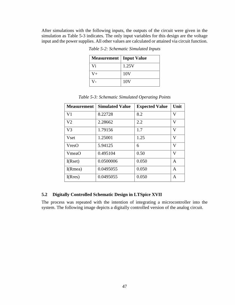
47
After simulations with the following inputs, the outputs of the circuit were given in the
simulation as Table 5-3 indicates. The only input variables for this design are the voltage
input and the power supplies. All other values are calculated or attained via circuit function.
Table 5-2: Schematic Simulated Inputs
Measurement Input Value
Vi 1.25V
V+ 10V
V- 10V
Table 5-3: Schematic Simulated Operating Points
Measurement Simulated Value Expected Value Unit
V1 8.22728 8.2 V
V2 2.28662 2.2 V
V3 1.79156 1.7 V
Vset 1.25001 1.25 V
VresO 5.94125 6 V
VmeaO 0.495104 0.50 V
I(Rset) 0.0500006 0.050 A
I(Rmea) 0.0495055 0.050 A
I(Rres) 0.0495055 0.050 A
5.2 Digitally Controlled Schematic Design in LTSpice XVII
The process was repeated with the intention of integrating a microcontroller into the
system. The following image depicts a digitally controlled version of the analog circuit.

48
Figure 5-2: Schematic of digitally controlled circuit
The voltage input will now be set by the microcontroller, and the outputs for the
measurements of the voltage across the resonator and resistor have been scaled using
divider and amplifier circuits, respectively, so that the values measured at VresO and
VmeaO will be within the voltage range for the microcontroller’s analog to digital
converter (0-3.3V). Using the values from Table 5-1, the following values can be added to
complete the above schematic.
Table 5-4: Additional sample schematic values
Name Value
Rp 1kΩ
Rdiv1 5kΩ
R7 1kΩ
R9 1kΩ
After simulations with the following inputs, the outputs of the circuit were given in the
simulation as Table 5-6 indicates. The only input variables for this design are the voltage
input and the power supplies. All other values are calculated or attained via circuit function.
Table 5-5: Schematic Simulated Inputs
Measurement Input Value
Vin 1.25V
V+ 10V
V- 10V
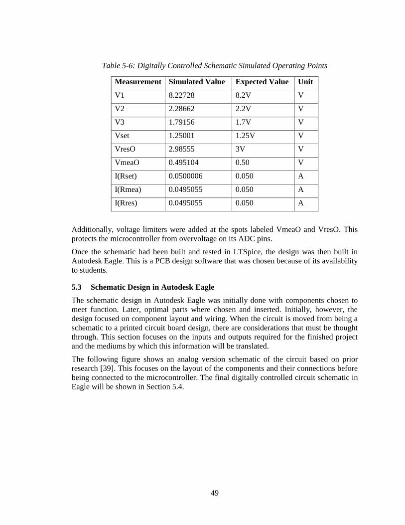
49
Table 5-6: Digitally Controlled Schematic Simulated Operating Points
Measurement Simulated Value Expected Value Unit
V1 8.22728 8.2V V
V2 2.28662 2.2V V
V3 1.79156 1.7V V
Vset 1.25001 1.25V V
VresO 2.98555 3V V
VmeaO 0.495104 0.50 V
I(Rset) 0.0500006 0.050 A
I(Rmea) 0.0495055 0.050 A
I(Rres) 0.0495055 0.050 A
Additionally, voltage limiters were added at the spots labeled VmeaO and VresO. This
protects the microcontroller from overvoltage on its ADC pins.
Once the schematic had been built and tested in LTSpice, the design was then built in
Autodesk Eagle. This is a PCB design software that was chosen because of its availability
to students.
5.3 Schematic Design in Autodesk Eagle
The schematic design in Autodesk Eagle was initially done with components chosen to
meet function. Later, optimal parts where chosen and inserted. Initially, however, the
design focused on component layout and wiring. When the circuit is moved from being a
schematic to a printed circuit board design, there are considerations that must be thought
through. This section focuses on the inputs and outputs required for the finished project
and the mediums by which this information will be translated.
The following figure shows an analog version schematic of the circuit based on prior
research [39]. This focuses on the layout of the components and their connections before
being connected to the microcontroller. The final digitally controlled circuit schematic in
Eagle will be shown in Section 5.4.

50
Figure 5-3: Schematic of analog circuit from [39]
5.3.1 Circuit Inputs
For this schematic design, there are several inputs. The resistance setpoint is set by the
user. The voltage input to the circuit, Vi, is controlled by the microcontroller’s programmed
PID control loop and is based on the resistance input. For powering the circuit, a bench
supply will be used to pass in a single voltage that will be stepped down according to the
necessary values. To connect this to the circuit, screw terminals will be used since they
allow for ease of connections to the bench supply.
The resonator will be connected to the circuit using four terminals to use Kelvin Sensing.
Essentially, the current is passed through different pins than the voltage is measured across.
This helps the measurement of the voltage across the resonator be more accurate by
eliminating the resistance of the leads used to measure the voltage.

51
5.3.2 Circuit Outputs
For this schematic design, the output will focus on the LCD screen. The resistance will be
displayed on this display and serves as the user output. The analog portion of the circuit
will feed its data into the microcontroller for digital control and programming.
5.3.3 Adding Libraries
While Eagle offers many different component footprints and symbols with the installation
of the program, not all components needed for this design are automatically included in the
Eagle software. Thus, components had to be added as necessary. This process is called
adding libraries. Prior to the beginning of this step, Ultra Librarian by Accelerated Designs
was installed to ensure smooth conversion of the downloaded model into a usable library
in Eagle. Version 8.1.204 was used for this project.
To begin importing libraries to Eagle, first, the BXL file was located. This is a binary Xlator
(BXL) file for the part that can be downloaded from many semiconductor company
websites. Since Texas Instruments components were used for this project, it was simple to
navigate this process. On their website page for the component to be used, there is a tab
called “Quality and Packaging”. On that page, there was a table named “CAD/CAE
symbols”. Then, there was a column called “CAD File (.bxl)”, and the correct part’s model
was selected and downloaded.
Next, the BXL file was opened in Ultra Librarian software. All CAD packages that were
not Eagle were unchecked. Then, “Export to Selected Tools” was clicked. The location of
the exported files was verified, Ultra Librarian was closed, and Eagle was opened. “File”,
then “New”, and then “Library” was selected. In the window that opens, “File” and then
“Execute Script” was selected. The “.scr” file that was exported from the previous step was
now opened and populated a new library.
Then, the part was closed. From the main control panel, “Library” and then “Open Library”
was selected. The library file (.lbr) was then opened, and then “Library” and “Create
Managed Library” was selected. Now, the downloaded part was listed as a component and
available to be used in the schematic.
5.4 Final Schematic Design
This section discusses the final schematic design incorporating the hardware power
requirements and DC-to-DC power conversions discussed within Section 5.4.1.

52
Figure 5-4: Final schematic design of analog portion
The top left component side has a relay in parallel with the resonator connector. The two
collections of two diodes, resistor, and capacitor on the right side of schematic are both
voltage limiters. The rest of the circuit follows the LTSpice schematic with the addition of
test points for testing the first revision of the PCB. They are pairs of test points so that
jumper wires can be used test each portion of the circuit for debugging.
5.4.1 Voltage Reference
An external voltage reference source is used for the DAC and ADC on the microcontroller.
For the ADC, the range of voltage it can read is 0-Vref/2, with Vref not exceeding 3.3V.
Thus, this project used a 3V reference source, with the component of choice being the
LM4050. The capacitors in the schematic limit noise to the system.
Figure 5-5: Final schematic design of voltage reference
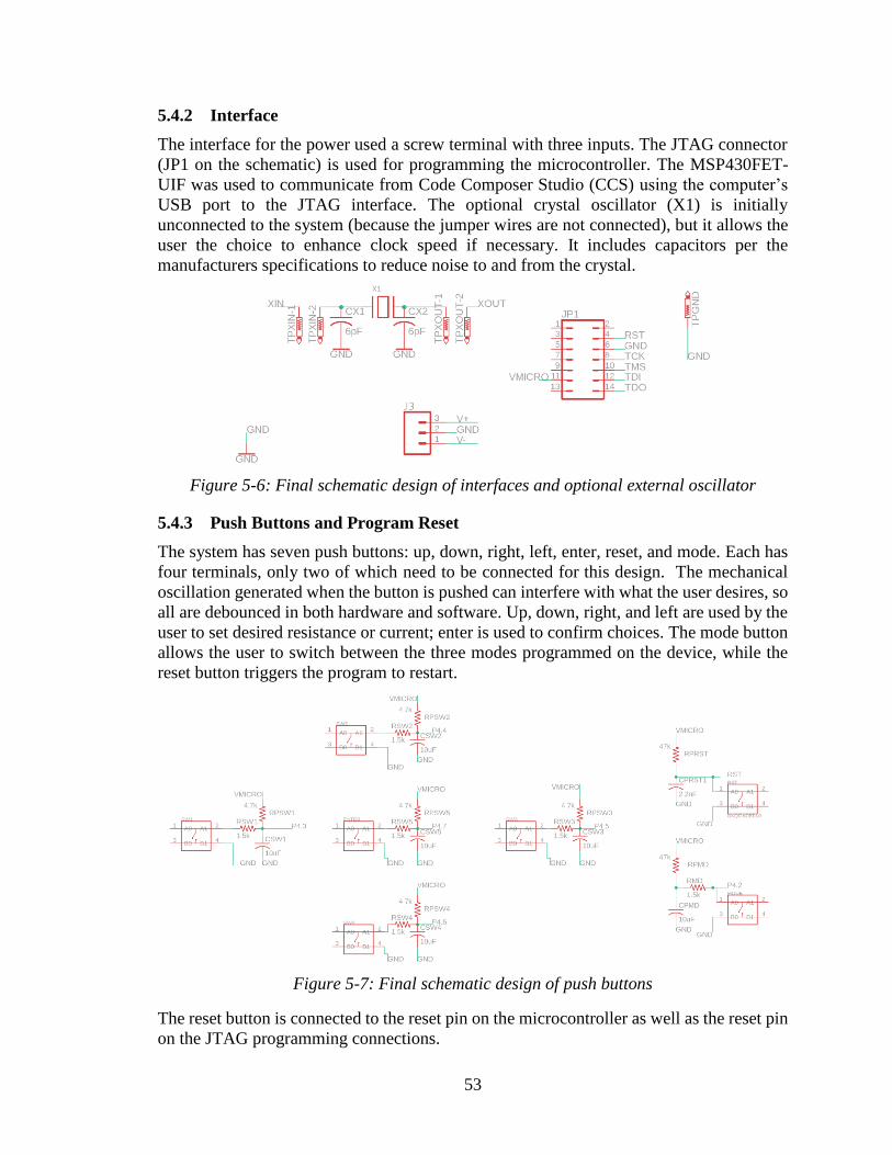
53
5.4.2 Interface
The interface for the power used a screw terminal with three inputs. The JTAG connector
(JP1 on the schematic) is used for programming the microcontroller. The MSP430FET-
UIF was used to communicate from Code Composer Studio (CCS) using the computer’s
USB port to the JTAG interface. The optional crystal oscillator (X1) is initially
unconnected to the system (because the jumper wires are not connected), but it allows the
user the choice to enhance clock speed if necessary. It includes capacitors per the
manufacturers specifications to reduce noise to and from the crystal.
Figure 5-6: Final schematic design of interfaces and optional external oscillator
5.4.3 Push Buttons and Program Reset
The system has seven push buttons: up, down, right, left, enter, reset, and mode. Each has
four terminals, only two of which need to be connected for this design. The mechanical
oscillation generated when the button is pushed can interfere with what the user desires, so
all are debounced in both hardware and software. Up, down, right, and left are used by the
user to set desired resistance or current; enter is used to confirm choices. The mode button
allows the user to switch between the three modes programmed on the device, while the
reset button triggers the program to restart.
Figure 5-7: Final schematic design of push buttons
The reset button is connected to the reset pin on the microcontroller as well as the reset pin
on the JTAG programming connections.
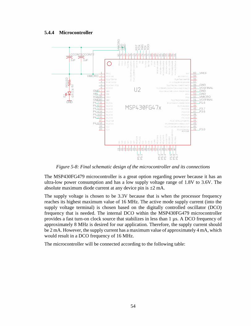
54
5.4.4 Microcontroller
Figure 5-8: Final schematic design of the microcontroller and its connections
The MSP430FG479 microcontroller is a great option regarding power because it has an
ultra-low power consumption and has a low supply voltage range of 1.8V to 3.6V. The
absolute maximum diode current at any device pin is ±2 mA.
The supply voltage is chosen to be 3.3V because that is when the processor frequency
reaches its highest maximum value of 16 MHz. The active mode supply current (into the
supply voltage terminal) is chosen based on the digitally controlled oscillator (DCO)
frequency that is needed. The internal DCO within the MSP430FG479 microcontroller
provides a fast turn-on clock source that stabilizes in less than 1 µs. A DCO frequency of
approximately 8 MHz is desired for our application. Therefore, the supply current should
be 2 mA. However, the supply current has a maximum value of approximately 4 mA, which
would result in a DCO frequency of 16 MHz.
The microcontroller will be connected according to the following table:

55
Table 5-7: Microcontroller Connections
Pin Number Pin Name Connection Function in Design
1 DVcc1 VMICRO Digital supply voltage, positive
terminal
7 GND Ground pin Ground pin
8 XIN Crystal in Optional external oscillator
connected via test pins
9 XOUT Crystal out Optional external oscillator
connected via test pins
10 GND Ground pin Ground pin
12 P4.6 SW4 Switch Four
13 P4.5 SW3 Switch Three
14 P4.4 SW2 Switch Two
15 P4.3 SW1 Switch One
18 P4.0 LCD RS Selects instruction or data
register
27 P5.0 LCD D0 First LCD data line
28 P5.1 LCD D1 Second LCD data line
34 P5.2 LCD D2 Third LCD data line
35 P5.3 LCD D3 Fourth LCD data line
36 P5.4 LCD D4 Fifth LCD data line
38 P5.5 LCD D5 Sixth LCD data line
39 P5.6 LCD D6 Seventh LCD data line
40 P5.7 LCD D7 Eighth LCD data line
41 P3.0 Relay Controls relay operation
47 P3.6 LCD E Starts data read/write
48 P3.7 LCD RW Selects read or write
50 P1.6 P1.6 DAC, inputs voltage to VCC for
current control
51 P1.5 VO2FINAL SD16 positive analog input A3
52 AVcc VMICRO Analog supply voltage, positive
terminal

56
53 AVss GND Analog supply voltage,
negative terminal
54 P1.4 GND SD16 negative analog input A3
55 P1.3 VO1FINAL SD16 positive analog input A4
56 P1.2 GND SD16 negative analog input A4
60 Vref Vref External reference voltage
70 TDO/TDI TDO Test data output port,
programming data input
terminal
71 TDI/TCLK TDI Test data input or test clock
input
72 TMS TMS Test mode select, input port for
device programming and test
73 TCK TCK Test clock (JTAG). TCK is the
clock input port
74 RST/NMI RST Reset input, will be connected
to toggle switch
78 DVss2 GND Digital supply voltage, negative
terminal
79 DVss1 GND Digital supply voltage, negative
terminal
80 DVcc2 VMICRO Digital supply voltage, positive
terminal
5.4.5 Display
Figure 5-9: Final schematic design of LCD

57
The TC1602A-09T will be used as the LCD screen for this project. The backlight supply
voltage for this component ranges from a minimum of 4.8V and a maximum of 5.2V, where
the typical supply voltage is 5V. In addition, the maximum supply current is 40mA and the
typical is 35mA [9].
Therefore, the LCD backlight supply voltage is chosen to be 5V as it falls perfectly between
the upper and lower bounds, and the supply current is chosen to be 35mA because that is
the typical operating values for this display.
Because of issues during testing with seeing 5V on some pins of the LCD that were directly
connected to the microcontroller, the logic level for the pins (set by VDD) was chosen to
range from 0-3.3V. However, to achieve proper contrast, a potentiometer connected to the
VO pin still needed to have about 5V of available voltage range. Thus, two diodes were
connected to one side of the potentiometer, allowing the potentiometer voltage range to go
from 3.3V to -1.4V, which is a range of 4.7V.
5.4.6 Relay Operation
In order to check if the current set by the system is actually within range, the first step of
the program is to short-circuit the resonator to ensure all is well before current is passed
through it. This is accomplished using a normally open relay.
Upon startup, the relay will close, the voltage across the 10Ω resistor will be measured, and
if the value is within a certain range, the relay will open, and current will then be forced to
pass through the resonator. Otherwise, it will stay closed to protect the resonator from
having an unexpected current pass through it.
Additionally, if the user disconnects the resonator at any point while the system is
operational, the program will register this and close the relay so that the instrumentation
amplifier is not trying to read the voltage across an open circuit and drawing lots of current
in the process.
The flyback diode protects the BJT from a voltage spike as the relay is activated and
deactivated. The BJT and its current gain activates the coil within the relay that will close
the relay when a voltage is applied to P3.0.
Figure 5-10: Schematic design of the relay
5.5 DC-to-DC Power Conversions
Several DC-to-DC conversions are needed to provide the components with the necessary
operating voltage and current values.
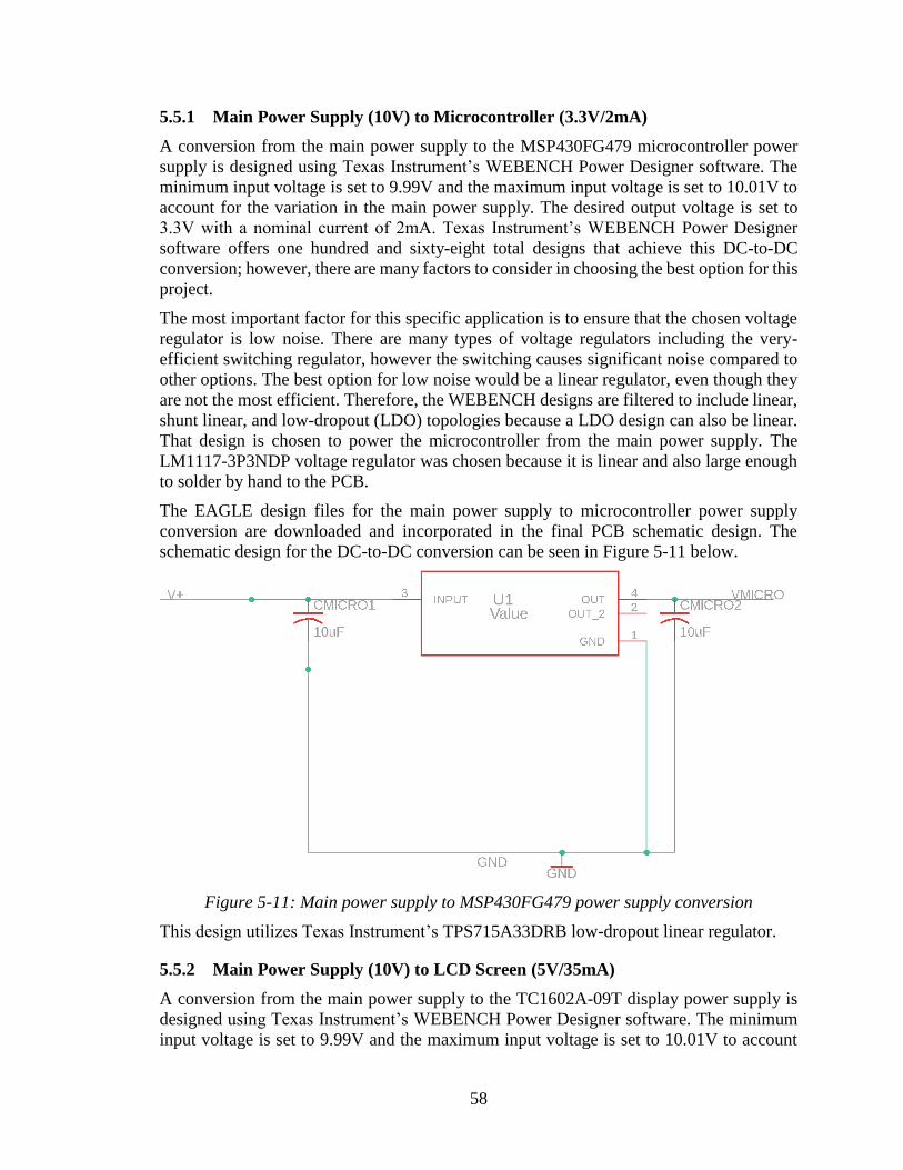
58
5.5.1 Main Power Supply (10V) to Microcontroller (3.3V/2mA)
A conversion from the main power supply to the MSP430FG479 microcontroller power
supply is designed using Texas Instrument’s WEBENCH Power Designer software. The
minimum input voltage is set to 9.99V and the maximum input voltage is set to 10.01V to
account for the variation in the main power supply. The desired output voltage is set to
3.3V with a nominal current of 2mA. Texas Instrument’s WEBENCH Power Designer
software offers one hundred and sixty-eight total designs that achieve this DC-to-DC
conversion; however, there are many factors to consider in choosing the best option for this
project.
The most important factor for this specific application is to ensure that the chosen voltage
regulator is low noise. There are many types of voltage regulators including the very-
efficient switching regulator, however the switching causes significant noise compared to
other options. The best option for low noise would be a linear regulator, even though they
are not the most efficient. Therefore, the WEBENCH designs are filtered to include linear,
shunt linear, and low-dropout (LDO) topologies because a LDO design can also be linear.
That design is chosen to power the microcontroller from the main power supply. The
LM1117-3P3NDP voltage regulator was chosen because it is linear and also large enough
to solder by hand to the PCB.
The EAGLE design files for the main power supply to microcontroller power supply
conversion are downloaded and incorporated in the final PCB schematic design. The
schematic design for the DC-to-DC conversion can be seen in Figure 5-11 below.
Figure 5-11: Main power supply to MSP430FG479 power supply conversion
This design utilizes Texas Instrument’s TPS715A33DRB low-dropout linear regulator.
5.5.2 Main Power Supply (10V) to LCD Screen (5V/35mA)
A conversion from the main power supply to the TC1602A-09T display power supply is
designed using Texas Instrument’s WEBENCH Power Designer software. The minimum
input voltage is set to 9.99V and the maximum input voltage is set to 10.01V to account
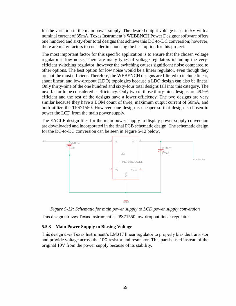
59
for the variation in the main power supply. The desired output voltage is set to 5V with a
nominal current of 35mA. Texas Instrument’s WEBENCH Power Designer software offers
one hundred and sixty-four total designs that achieve this DC-to-DC conversion; however,
there are many factors to consider in choosing the best option for this project.
The most important factor for this specific application is to ensure that the chosen voltage
regulator is low noise. There are many types of voltage regulators including the very-
efficient switching regulator, however the switching causes significant noise compared to
other options. The best option for low noise would be a linear regulator, even though they
are not the most efficient. Therefore, the WEBENCH designs are filtered to include linear,
shunt linear, and low-dropout (LDO) topologies because a LDO design can also be linear.
Only thirty-nine of the one hundred and sixty-four total designs fall into this category. The
next factor to be considered is efficiency. Only two of those thirty-nine designs are 49.9%
efficient and the rest of the designs have a lower efficiency. The two designs are very
similar because they have a BOM count of three, maximum output current of 50mA, and
both utilize the TPS71550. However, one design is cheaper so that design is chosen to
power the LCD from the main power supply.
The EAGLE design files for the main power supply to display power supply conversion
are downloaded and incorporated in the final PCB schematic design. The schematic design
for the DC-to-DC conversion can be seen in Figure 5-12 below.
Figure 5-12: Schematic for main power supply to LCD power supply conversion
This design utilizes Texas Instrument’s TPS71550 low-dropout linear regulator.
5.5.3 Main Power Supply to Biasing Voltage
This design uses Texas Instrument’s LM317 linear regulator to properly bias the transistor
and provide voltage across the 10Ω resistor and resonator. This part is used instead of the
original 10V from the power supply because of its stability.

60
Figure 5-13: Schematic for main power supply to biasing power supply conversion
5.6 Printed Circuit Board Hardware Power Requirements
To begin the PCB schematic design process, the hardware’s voltage and current
requirements are first evaluated to ensure each component receives the required amount of
power. Beginning with the main power supply, it will need to be stepped down several
times to meet each component’s power needs.
5.6.1 Main Power Supply
The target supply voltage for this design is ±10V. The main power supply source will be
the Agilent E3631A triple output DC power supply. One terminal will be set to +10V and
a second terminal will be set to -10V.
The change in output voltage for any line/load change (within the datasheet limitations) is
given by <0.01% + 2 mV. Therefore, since the main power supply is set to ±10V then the
change in voltage will range from ±9.997V to ±10.003V [32].
5.6.2 Instrumentation Amplifiers
The instrumentation amplifier chosen for this project was the INA828. It requires a supply
voltage of ±2.25V to ±18V. However, the nominal voltage supply at 25°C (which is
assumed to be the room temperature when operating this device) is ±15V. The input voltage
can range from V- + 2V to V+ - 2V. The absolute maximum current to the signal input
terminals is 10mA. The typical current for the power supply is ±10 mA, and the maximum
is ±12 mA [18].
Given these voltage and current ranges, the voltage supply is confirmed to be ±10V because
it matches the main power supply voltage and remains within the operating range of the
amplifier.
5.6.3 Voltage to Current Converter
The OPA828 operational amplifier will be used for the voltage to current converter. It has
a supply voltage of ±2.25V to ±18V. The maximum current for the input signals is 10mA.
The typical power supply current is 5.5mA while the maximum is 7.1mA with an ambient
temperature between 0 °C to 85 °C [40]. Therefore, the voltage supply is confirmed to be
±10V because it parallels the main power supply voltage and remains within the operating
range.

61
5.6.4 Overall Voltage Supply Design
This section shows the overall voltage supply design for the project. Table 5-8 lists
all of the voltages needed from the components and circuit schematic design.
Table 5-8: Circuit Voltage Supplies
Figure 5-14 shows the voltage supply block diagram.
Figure 5-14: Voltage supply block diagram
5.6.5 Power Supply for Components
After analyzing each component individually, the final chosen power supply values for
each component can be found in Table 5-9.

62
Table 5-9: Voltage and Current for Components
Part Number Power Supply
Voltage
Power Supply
Current
Maximum
Supply Current
INA828 ±10V Expected ±10mA ±12mA
MSP430FG479 3.3V 2mA 4mA
OPA828 ±10V Expected ±5.5mA ±6.5mA
TC1602A-09T 5V 35mA 40mA
5.7 Designing the PCB in Eagle
This section details the design of the printed circuit board.
5.7.1 Physical Component Layout
Once the schematic design has been completed, the board must also be designed, and the
ideal electrical model must be converted into a useable circuit board. For this step, the
components must be arranged so that the inputs and outputs are easily accessible.
5.7.2 Grounding
The grounding for the circuit will include a ground pour on the top and bottom layers. This
ground pour layer is used for heat sinking and easier connections to ground. With these
layers in place, grounding a component is as simple as creating a via and labeling it “GND”.
This will allow for connections to the ground pours.
5.7.3 Routing
The PCB routing for the project has been done in Autodesk EAGLE. This has been done
using a combination of manual and auto routing. For this circuit, the design rule check
(DRC) must be satisfied. This is a list of the design requirements for the manufacturer
regarding details such as trace widths, clearances, and other similar details. The PCB
manufacturer chosen for this project have DRC requirements listed in the following table.

63
Table 5-10: Manufacturer Routing Specifications
Requirement Minimum Value (Mils)
Inner layer clearance 10”
Copper to edge of PCB 10” (outer layers), 15-20”
(inner layers)
Pad size 10” (finished hole size for
vias), 14” (finished hole
size for component holes)
Annular ring 5” (for vias), 7” (for
component holes)
Hole size ±5”
PCB Thickness 20” (2 or 4-Layer), 31” (6-
Layer), 47” (8-Layer), 62”
(10-layer)
Outer layer tolerances ±10”
Copper trace width 5” (1 oz. finished copper
weight), 6” (2 oz. finished
copper weight), 10” (3 oz.
finished copper weight),
12” (4 oz. finished copper
weight)
Air gap ±20% or ±2” (whichever is
greater)
Soldermask swell 2.5” on each side
Slot width 31”
Tab rout spacing 100”
Silkscreen (legend)
minimum line width
5”
The different requirements for the DRC are described here. “Inner layer clearance” is the
distance that the through holes on multilayer boards have to be cleared from internal planes.
“Copper to edge of PCB” is the distance between the edge of the board and the pattern.
Traces connecting different layers use vias, usually placed on a pad. “Pad size” is the
minimum width of the pad for the vias. The “Annular ring” is the area of a pad that
surrounds a via. “Hole size” is the width of the finished holes in the board after the drills
have been completed. “PCB thickness” describes in the minimum thickness of the overall
board.

64
“Outer layer tolerances” refer to the routing of the circuit. The “Copper trace width”
describes the distance between two conductive copper lines that will carry current in the
circuit. This value is related to the weight of the copper. “Air gap” is the distance between
two adjacent traces. This distance is crucial because of the heat generated by current in a
circuit. If two traces are too close together and heat up because of the current passing
through them, an issue may arise. “Soldermask swell” refers to the width by which solder
mask will expand. The solder mask is a protective layer places on the bare PCB to prevent
accidental bridging during assembly. It is what gives the board its distinct color. This will
expand throughout production. Thus, it is important to have extra clearance around the
edges of the PCB so that there is no shorting when this occurs.
“Slot width” describes the width of a slot in the board. Although similar to an elongated
hole, these have a different minimum width because different tools are often used for
drilling the slots (mills for slots and drills for tools). Some slots will be covered in metal,
while others will be left unmetallized. “Tab rout spacing” is the distance between different
tab routes. These can be used when the manufacturer combines several boards together into
a panel of PCBs. Essentially, the designs can then be snapped apart using perforated
breakaway tabs instead of having to cut them. This is an alternative to creating smaller
boards entirely separately. The “Silkscreen (legend)” refers to the layer on top of the PCB
that designates the different part numbers.
The following image depicts the finished routing of the printed circuit board for the project.
This configuration satisfies the DRC and has ground pours. The red is a copper ground
pour on the top layer, and the blue is a bottom layer copper ground pour.
Figure 5-15: Current routed PCB image

65
5.7.4 Gerber File Generation
Gerber files are used by the PCB manufacturers to create the board. They can be generated
in the design software (EAGLE). There are a number of checks and ways to minimize
errors for this step. Some common errors, as listed by the PCB manufacturers, are a missing
aperture list (that describes which tool to use), a missing excellon drill file (that describes
hole size and location), a missing tool list (which details what tools are needed for drilling
holes), insufficient annular ring (when a drill pierces a copper layer because of improper
annular ring specifications), an insufficient copper trace width, and insufficient inner
clearances. Minimizing these errors will aid in the creation of the PCB.
The following figure shows an image of what the Gerber file is creating in its “Top Copper”
file. This is the copper layer that will be on the top layer of the PCB.
Figure 5-16: Top Copper layer from Gerber File
The following steps can be used to generate the Gerber files in EAGLE. First, the board
file (.brd) was opened in EAGLE. Next, “File” and then “Cam Processor…” was selected.
After that, the “Local CAM jobs” button in the top left was selected, and the
“gerb274x.cam” was selected. Make sure it’s not trying to run legacy CAM process. If it
is, just double click on each of the circular arrow icons under the category “Legacy”. Next,
“Process Job” was selected. A new folder was created for the location of the files.
The following steps can be used to generate the drill file in EAGLE. First, the board file
(.brd) was opened in EAGLE. Next, “File” and then “Cam Processor…” was selected.
After that, the “Local CAM jobs” button in the top left was selected, and the
“excellon.cam” was selected. It was double checked to verify that it is trying to run legacy
CAM process. Next, “Process Job” was selected. The files were placed in the same folder
as before.
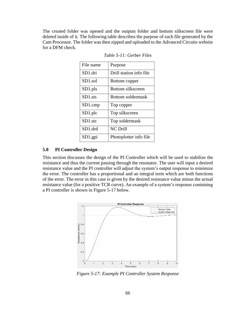
66
The created folder was opened and the outputs folder and bottom silkscreen file were
deleted inside of it. The following table describes the purpose of each file generated by the
Cam Processor. The folder was then zipped and uploaded to the Advanced Circuits website
for a DFM check.
Table 5-11: Gerber Files
File name Purpose
SD1.dri Drill station info file
SD1.sol Bottom copper
SD1.pls Bottom silkscreen
SD1.sts Bottom soldermask
SD1.cmp Top copper
SD1.plc Top silkscreen
SD1.stc Top soldermask
SD1.drd NC Drill
SD1.gpi Photoplotter info file
5.8 PI Controller Design
This section discusses the design of the PI Controller which will be used to stabilize the
resistance and thus the current passing through the resonator. The user will input a desired
resistance value and the PI controller will adjust the system’s output response to minimize
the error. The controller has a proportional and an integral term which are both functions
of the error. The error in this case is given by the desired resistance value minus the actual
resistance value (for a positive TCR curve). An example of a system’s response containing
a PI controller is shown in Figure 5-17 below.
Figure 5-17: Example PI Controller System Response

67
Notice how there can be a significant overshoot from the desired value. There is a tradeoff
with PI controllers between the maximum overshoot and the rise time. This means that in
order to minimize the maximum overshoot, then there will be a longer rise time for the
system to rise to the desired value. In order to approximate values for the proportional gain
(𝐾𝑝) and the integral gain (𝐾𝑖) for the PI controller, the control system’s transfer function
must be found. The block diagram given in Figure 5-18 is used to find the control system’s
transfer function
Figure 5-18: Control System Block Diagram
The PI controller’s transfer function is given by 𝑃𝐼(𝑠) = 𝐾𝑝 +𝐾𝑖
𝑠. The resonator’s transfer
function is unknown and different for each device. This project is intended to work for
different types of resonators so approximations will need to be made to account for this.
The resonator’s transfer function is approximated by a first order transfer function to be
𝑅(𝑠) =𝑏
𝑠+𝑎 where ‘b’ and ‘a’ are constants that vary for each resonator. Now, the control
system’s transfer function can be found using Figure 5-18.
𝑇(𝑠) =𝐴𝑐𝑡𝑢𝑎𝑙 𝑅𝑒𝑠𝑖𝑠𝑡𝑎𝑛𝑐𝑒
𝐷𝑒𝑠𝑖𝑟𝑒𝑑 𝑅𝑒𝑠𝑖𝑠𝑡𝑎𝑛𝑐𝑒=
𝑃𝐼(𝑠) ∗ 𝑅(𝑠)
1 + [𝑃𝐼(𝑠) ∗ 𝑅(𝑠)]
The transfer functions for PI(s) and R(s) are then substituted to give the transfer function
𝑇(𝑠) =𝑏(𝐾𝑝𝑠 + 𝐾𝑖)
𝑠2 + (𝑎 + 𝑏𝐾𝑝)𝑠 + 𝑏𝐾𝑖
The denominator of the transfer function is the system’s characteristic equation.
A general second-order system transfer function is given by:
𝐶(𝑠) = 𝐾 ∗𝜔𝑛
2
𝑠2 + 2ζ𝜔𝑛𝑠 + 𝜔𝑛2
Where K is the system’s desired steady state value, ζ is the damping ratio, and 𝜔𝑛 is the
undamped natural frequency. For an undamped system ζ = 0, for an underdamped system
0 < ζ < 1, for a critically damped system ζ = 1, and for an overdamped system ζ > 1. For
the project application, a underdamped response is desired because it allows for the fastest
rise time. The denominator of the general transfer function is the desired characteristic
polynomial of the control system, so the system’s characteristic equation is set equal to this
then solved for the proportional gain (𝐾𝑝) and the integral gain (𝐾𝑖).
𝑠2 + (𝑎 + 𝑏𝐾𝑝)𝑠 + 𝑏𝐾𝑖 = 𝑠2 + 2ζ𝜔𝑛𝑠 + 𝜔𝑛2
By comparing coefficients for the ‘s’ term, 𝐾𝑝 is found.

68
𝑎 + 𝑏𝐾𝑝 = 2ζ𝜔𝑛 → 𝐾𝑝 =2ζ𝜔𝑛 − 𝑎
𝑏
By comparing the constant terms, 𝐾𝑖 is found.
𝑏𝐾𝑖 = 𝜔𝑛2 → 𝐾𝑖 =
𝜔𝑛2
𝑏
Keep in mind, the resonator’s transfer function was approximated by a first order transfer
function to be 𝑅(𝑠) =𝑏
𝑠+𝑎 where ‘b’ and ‘a’ are constants that vary for each resonator. The
‘b’ term depends on the resonator’s highest resistance value when applied with a unit pulse
whereas ‘a’ depends on the output’s rate of exponential decay when applied with a unit
pulse. Therefore, the proportional gain (𝐾𝑝) and the integral gain (𝐾𝑖) are both inversely
related to the resonator’s resistance. To test these theories, constants are applied to 𝐾𝑝 and
𝐾𝑖 where 𝐾𝑝=0.02 and 𝐾𝑖 = 0.002. The maximum overshoot is analyzed when the
different resistance values are used in place of the resonator. If 𝐾𝑝 and 𝐾𝑖 and inversely
related to resistance, it is expected that the maximum overshoot will increase as the
resistance increases which means that the gains need to decrease as resistance is increased
(instead of being constants). The data is graphed and shown in Figure 5-19.
Figure 5-19: Control measurements using constant gain values
Notice how the maximum overshoot increases as the resistance increases which means that
the gains need to decrease as resistance is increased.

69
5.8.1 Maximum Overshoot
The maximum overshoot is defined as the peak value of the system response and can be
expressed as a percentage relative to the steady-state value. After the PI controller gains
are set to be inversely dependent on the resistance of the resonator, the maximum overshoot
is evaluated with different resistor values.
Figure 5-20: Maximum overshoot of 15Ω Resistor
The maximum overshoot is found to be 1% or less for the 15Ω Resistor.
Figure 5-21: Maximum overshoot of 22Ω Resistor
The maximum overshoot is found to be 2.5% or less for the 22Ω Resistor.
The maximum overshoot was found to be very low, however this could mean that the
system’s time response could be very slow. If it is desired to lower the maximum overshoot,
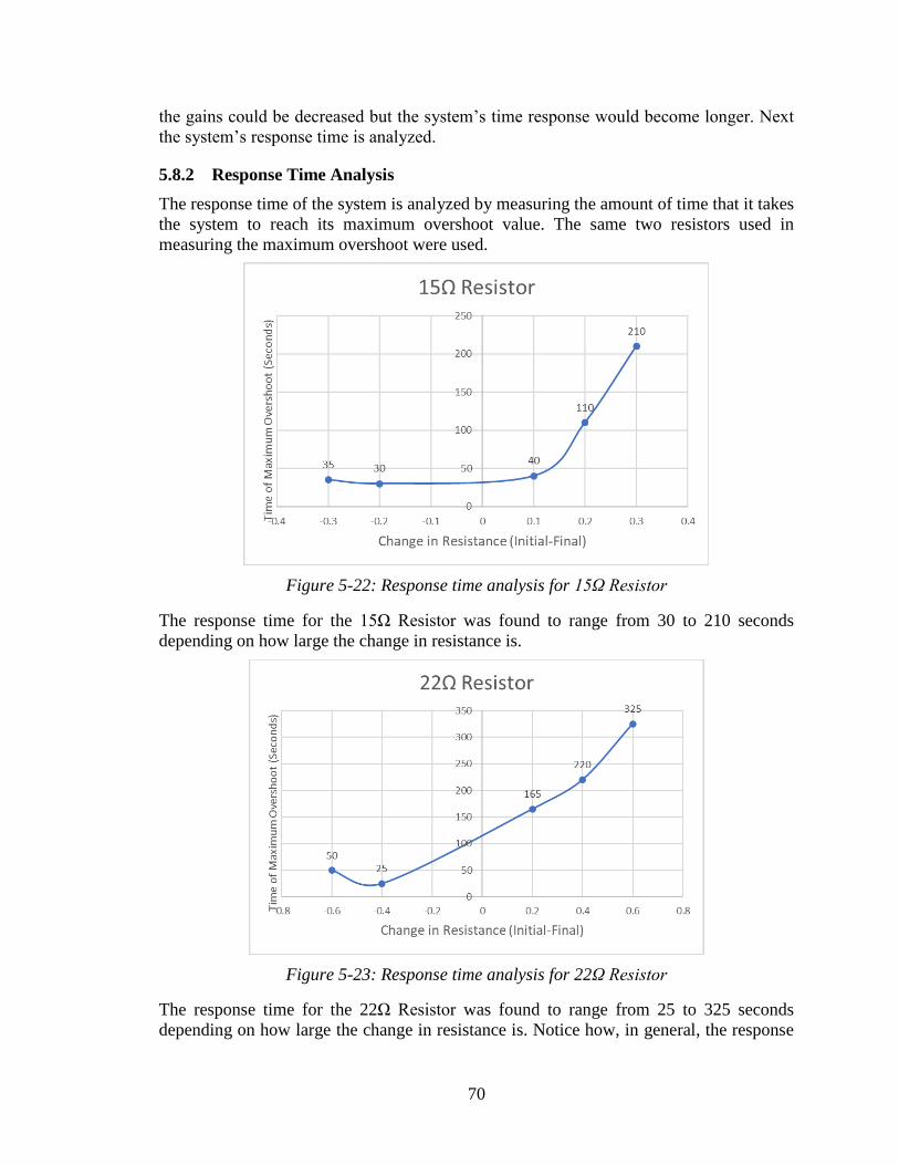
70
the gains could be decreased but the system’s time response would become longer. Next
the system’s response time is analyzed.
5.8.2 Response Time Analysis
The response time of the system is analyzed by measuring the amount of time that it takes
the system to reach its maximum overshoot value. The same two resistors used in
measuring the maximum overshoot were used.
Figure 5-22: Response time analysis for 15Ω Resistor
The response time for the 15Ω Resistor was found to range from 30 to 210 seconds
depending on how large the change in resistance is.
Figure 5-23: Response time analysis for 22Ω Resistor
The response time for the 22Ω Resistor was found to range from 25 to 325 seconds
depending on how large the change in resistance is. Notice how, in general, the response

71
time of the 22Ω resistor is much larger than the 15Ω resistor. This is because the gain
values of the PI controller are inversely dependant on the resistance so as the resistance
increases then the gains decrease so it takes longer to rise.
5.9 Introduction to Software Design
The software component of this project is implemented on the Texas Instruments
MSP430FG479 mixed-signal microcontroller. The agile methodology was applied to the
development process to encourage organization and timeliness. The main tasks of the
microcontroller include outputting the desired voltage to the circuit and reading in the
relevant voltage measurements across certain terminals. The program loaded to the
microcontroller carries out the following objectives: calculates the resistance from the
voltage values read in by the microcontroller and updates the LCD, communicates
information between the user and the device and controls the current passed through the
circuit.
5.10 Agile Methodology
The agile software development and project management approach was embraced by the
team in the development of the microcontroller code for the resistance control system. The
agile method emerged relatively recently as a new framework to creating software that
addresses the unpredictability of developing software. Furthermore, it places an emphasis
on adaptive planning, early delivery, continuous improvement and the ability to respond
efficiently to change. The benefits of agile development include the delivery of high
product quality and client satisfaction, enhanced project control and reduced risks. Since
this was the team’s first time implementing some of the technologies used in this project,
there was potential for particular components to not be compatible with the desired system
and need to be substituted. Furthermore, there was also a possibility that chosen software
libraries or testing environments were not be well-suited to support the application. The
agile approach enabled this team to efficiently react to change by frequently evaluating
completed tasks and gathering feedback.
5.10.1 Conventional Agile Methodology
The conventional agile methodology implements iterative sequences of planning,
designing, implementing, testing and feedback to a project in order to appropriately
respond to the ever-changing realm of software development. The method progresses
through this planning to testing loop until a deliverable is achieved, and this applies to each
phase of development. This process allowed for the team to continuously adapt to new
changes or knowledge.
Furthermore, the team utilized the scrum framework within the agile method of
development to manage the software development process. The scrum framework
encourages flexibility and not micromanaging as it implies that the software team or lead
is responsible for delivering a working product as opposed to the manager or project lead
providing detailed instructions regarding the task at hand. In addition, the team working
within a scrum environment becomes cross-functional which lends to a self-organizing and
collaborative team. The ideals and practices of this framework fit this team well.

72
In scrum development, the creation of the software for the microcontroller was divided into
multiple sprints. A sprint is a time interval allotted and designated to a specific project task.
The length of the sprint was dependent on the level of complexity of the task but was about
one to two weeks on average. At the beginning and end of each sprint, the team held a
meeting led by the scrum master in order to gauge the task project and discuss any changes
or obstacles. The role of the scrum master was assigned to the software lead, Michaela
Pain. This framework added structure to the software development process and ensured
that the defined tasks were being implemented on a semi-weekly basis. In addition, it
encouraged a designated group meeting for software specifically on a frequent basis.
Furthermore, the use of this methodology was beneficial to every group member because
it is extensively utilized within the software development practice. It is advantageous to
have experience with this type of framework prior to delving into the industry as many
companies have embraced or are in the process of embracing this process. Lastly, the agile
methodology is not only applicable to software development. It was used in the software
component of this project and was evaluated to extend its usefulness to other parts of the
project.
5.11 Software Functionality
The purpose of the software can be divided into the following three tasks: calculating the
resistance of the resonator, communicated information to the user, and controlling the
current passed into the resistor. These tasks will be accomplished through functions
programmed into the microcontroller.
5.11.1 Functional Modes
The microcontroller program operates in three modes: standby, characterization and
operational. This was a feature requested by the research group under Dr. Abdolvand. The
standby mode limits the program loop to read relevant resistor values and output the
calculated resistance to the LCD screen. The characterization mode allows the user to input
a desired current value for the circuit to operate at and then continuously calculates the
resistance and current and output them to the display. The operational mode allows the user
to input the desired resistance value for the program to stabilize the resonator at and
performs the necessary calculations to determine the current for the next iteration of the
loop. The operational mode continues to calculate the resistance and current to display to
the user throughout the process. This allows the user to control whether the device is
operating to stabilize the temperature or to simply display the state of the resonator in terms
of resistance and temperature to the user. In addition, it conserves power without sacrificing
the time to power down and startup the device again. This contributes to the low-power
quality of the application when the program is in standby mode.
5.11.2 User Interface
The LCD is used to communicate information between the microcontroller and the user.
When the program begins, the user is prompted with a message to indicate that the device
is performing checks on the second line of the display. Then, the program displays the
calculated resistance to the first line since this is the primary information. The user is
prompted to select a mode which appears on the second line once the checks and
initialization steps are complete. The resistance is continuously being updated on the first

73
line while the mode name is changed every time the user selects the mode button. The
mode is selected once the user selects the enter button.
Within the standby mode, the program continuously calculates the resistance and output
the result to the screen. The user does not provide any input unless the user wants to exit
the loop. The mode button sends the user back to the mode selection menu.
Within the characterization mode, the program allows the user to select a desired current
to output to the circuit. The program uses a blinking cursor to designate the position that
the buttons control. The up and down buttons let the user increase or decrease the value at
that position while the left and right buttons let the user select the position. The user presses
enter in order to submit their choice. The program flags an error if the desired current value
is not within the appropriate range. Otherwise, the cursor will turn off and the resistance
will update on the LCD. The user does not provide any other input unless the user wants
to exit the loop. The mode button sends the user back to the mode selection menu while
the up button sends the user back to the desired current selection menu.
Within the operational mode, the program allows the user to select a desired resistance to
stabilize the resonator at. Similar to the characterization mode, the program uses the cursor
to designate the position that the buttons control. The up and down buttons modify the
value at the position indicated by the cursor while the left and right buttons modify the
position. This value is submitted when the enter button is pressed. The program flags an
error if the desired resistor value is not within the appropriate range given the calculated
TCR. Otherwise, the cursor will turn off and the resistance will be updated. In addition, the
updating current will output to the second line in order to display the actions of the control
loop. The user does not provide any more input unless the user wants to exit the loop. The
mode button sends the user back to the mode selection menu while the up button sends the
user back to the desired resistance selection menu.
At any time during the program, if the device is removed, the program flags an error that
stops the program flow. The user is prompted to replace the device and press enter. Upon
pressing enter, the program restarts.
5.12 Algorithm Overview
The main tasks of the program are implemented in five main functions. The tasks are
divided as follows: initialization, read mode, resistance calculation, standby mode,
characterization mode and operational mode. The initialization function prepares the
program and device for the main functionality. The read mode function allows the user to
click through the available modes and select one. The resistance calculation function
performs the various voltage reads and conversions to achieve the resistance of the
resonator. The standby mode function continuously outputs the updated resistance to the
user. The characterization mode function allows input from the user regarding the desired
current value applied to the circuit and continuously refreshes the resistance. The
operational mode allows input from the user regarding the desired resistance value,
continuously calculates the new current value to achieve the desired resistance and outputs
the resistance continuously throughout the process.
All constants and variables are defined for each objective. In addition, the initial values for
the inputs and outputs along with any external libraries are initialized at the top of the

74
program. Global variables are used for the resistance, current, voltage and TCR because
they will need to be used between functions. Since the program implements these functions
sequentially, there is no concern for these variables to be overwritten and cause an issue.
Below, each function is defined by its procedure to show the processor compilation
sequence and program logic.
5.12.1 Initialization
The purpose of this task is to initialize the components of the software and perform checks
to ensure sound performance. This is done by first clearing the LCD screen using the
function provided by the C library used for interfacing the HD44780 controller built-in to
the display. This ensures that no residual text remains on the screen from a previous
program run. The program outputs a message to the user on the second line regarding the
program running checks before further execution. Then, the circuit is checked by setting
the relay to high and ensuring that the measured current through the resistor is the same as
the expected current. The measured current is compared to be within 30% of the expected
circuit. The relay is set back to low if it is; however, if it is not, then the program will
display an error message to the user and enter an infinite loop to prevent the program from
continuing. Then, the program outputs a small voltage and delays the program to allow for
the system to adapt. Next, it measures the resistance and subsequently outputs a larger
voltage, delays and measures the resistance. These resistance measurements are displayed
to the first line of the LCD after each calculation. This program takes the difference
between these two values to determine whether the resistor has a positive or negative TCR
value. The program outputs the small voltage again before allowing the user to select a
mode. The measured resistance value is refreshed while the user is in the mode selection
process.
5.12.2 Resistance Calculation
The purpose of this task is to calculate the value of the resistance of the resonator. The
determination of the resistance requires four main steps: determine the voltage across
RMEA, calculate current through RMEA, determine the voltage across the resonator and
calculated the resistance of the resonator. RMEA is a 10Ω 0-TCR resistor that is in series
with the resonator. Thus, the current through RMEA is the same current flowing through the
resonator. To calculate the current, the voltage across the resistor is measured and Ohm’s
Law is applied. Then, the voltage across the resonator is measured in order to have enough
information to apply Ohm’s Law to calculate the resistance of the resonator.
To determine the voltage across RMEA, one of the 16-bit ADC channels on the
microcontroller is used. This voltage has been wired to be associated with channel 3. The
channel is configured by setting the appropriate bits to output, enabling the appropriate
channel and selecting the polling mode. To rid the results of deviations caused by noise,
more than one hundred results are read in and eventually averaged. The value read in by
the microcontroller is converted to a voltage value in volts. Within this function resides the
check to determine whether the device has been removed. The function verifies that the
voltage is sufficiently large. When the voltage is read in as low, an error is output to the
user prompting the user to hold enter when a new connection is made. Then, the program
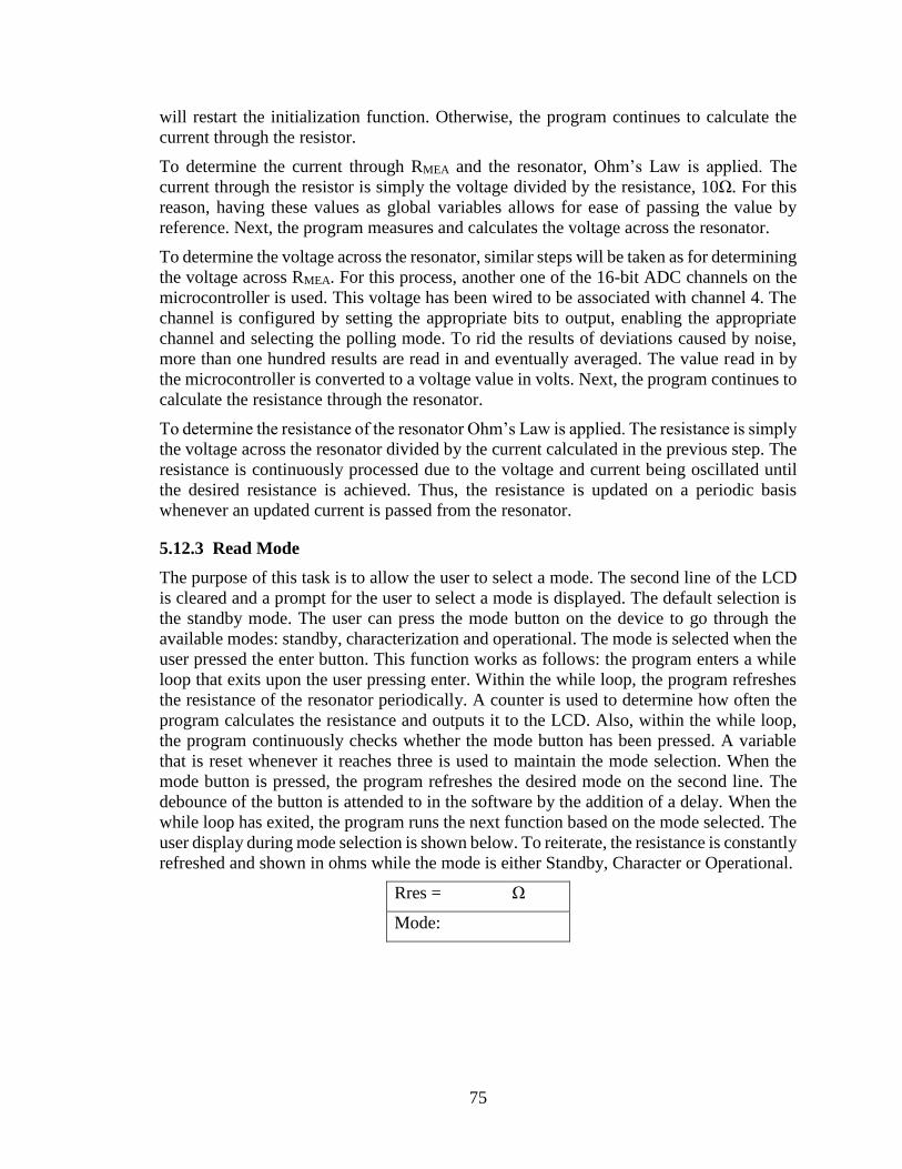
75
will restart the initialization function. Otherwise, the program continues to calculate the
current through the resistor.
To determine the current through RMEA and the resonator, Ohm’s Law is applied. The
current through the resistor is simply the voltage divided by the resistance, 10Ω. For this
reason, having these values as global variables allows for ease of passing the value by
reference. Next, the program measures and calculates the voltage across the resonator.
To determine the voltage across the resonator, similar steps will be taken as for determining
the voltage across RMEA. For this process, another one of the 16-bit ADC channels on the
microcontroller is used. This voltage has been wired to be associated with channel 4. The
channel is configured by setting the appropriate bits to output, enabling the appropriate
channel and selecting the polling mode. To rid the results of deviations caused by noise,
more than one hundred results are read in and eventually averaged. The value read in by
the microcontroller is converted to a voltage value in volts. Next, the program continues to
calculate the resistance through the resonator.
To determine the resistance of the resonator Ohm’s Law is applied. The resistance is simply
the voltage across the resonator divided by the current calculated in the previous step. The
resistance is continuously processed due to the voltage and current being oscillated until
the desired resistance is achieved. Thus, the resistance is updated on a periodic basis
whenever an updated current is passed from the resonator.
5.12.3 Read Mode
The purpose of this task is to allow the user to select a mode. The second line of the LCD
is cleared and a prompt for the user to select a mode is displayed. The default selection is
the standby mode. The user can press the mode button on the device to go through the
available modes: standby, characterization and operational. The mode is selected when the
user pressed the enter button. This function works as follows: the program enters a while
loop that exits upon the user pressing enter. Within the while loop, the program refreshes
the resistance of the resonator periodically. A counter is used to determine how often the
program calculates the resistance and outputs it to the LCD. Also, within the while loop,
the program continuously checks whether the mode button has been pressed. A variable
that is reset whenever it reaches three is used to maintain the mode selection. When the
mode button is pressed, the program refreshes the desired mode on the second line. The
debounce of the button is attended to in the software by the addition of a delay. When the
while loop has exited, the program runs the next function based on the mode selected. The
user display during mode selection is shown below. To reiterate, the resistance is constantly
refreshed and shown in ohms while the mode is either Standby, Character or Operational.
Rres = Ω
Mode:
76
5.12.4 Standby Mode
The purpose of this task is to implement the standby mode functionality. The standby mode
outputs a string indicating that standby mode has been selected. Then, it outputs a default
voltage to the circuit and provides a delay to allow the voltage to be applied to the entire
circuit. Next, it enters a loop that continuously determines the resistance and outputs it to
the display.
5.12.5 Characterization Mode
The purpose of this task is to implement the characterization mode functionality. The
characterization mode outputs a string indicating that characterization mode has been
selected. Then, it prompts the user to input a desired current by showing zeros representing
the modifiable values with a cursor on the first zero. Within a loop, the program
continuously checks whether any of the buttons are pressed. The left button will move the
cursor and modifiable position in the desired current to the left. The right button will move
the cursor and modifiable position in the desired current to the right. The up button will
increase the value at the current position in the desired current. The down button will
decrease the value at the current position in the desired current. The mode button will send
the user back to the mode selection menu. The enter button will submit the desired current
to be converted to a floating-point variable that can be used by the program. Meanwhile,
within this loop, the resistance is calculated and output to the display. Once the user submits
their desired current, the program calculates the maximum current. The program will flag
an error if the input is too high and direct the user back to selecting an input. Otherwise,
the current is converted to a voltage and output to the circuit. A delay is used to ensure that
the output voltage has time to stabilize. Then, the program enters a loop that continuously
calculates the resistance of the resonator and outputs the resistance and corresponding
current. In addition, within the loop, the program checks whether mode or up is pressed. If
the former, then the user is able to select a new mode. If the latter, then the user is able to
select a new desired current value.
5.12.6 Operational Mode
The purpose of this task is to implement the operational mode functionality. The
operational mode calculates a current using a PI controller to pass through the circuit to
achieve the desired resistance. The program will feed the desired values into a PI controller
to appropriately maintain the resistance. Further, it will perform the calculation and output
the new current that will be converted to a voltage to be output to the circuit. This current
will then be passed into the resonator, and the next iteration will begin. The mode outputs
a string indicating that operational mode has been selected. Then, it prompts the user to
input a desired resistance by showing zeros representing the modifiable values with a
cursor on the first zero. Within a loop, the program continuously checks whether any of
the buttons are pressed. The left button will move the cursor and modifiable position in the
desired current to the left. The right button will move the cursor and modifiable position in
the desired current to the right. The up button will increase the value at the current position
in the desired current. The down button will decrease the value at the current position in
the desired current. The mode button will send the user back to the mode selection menu.
The enter button will submit the desired current to be converted to a floating-point variable
77
that can be used by the program. Meanwhile, within this loop, the resistance is calculated
and output to the display. Once the user submits their desired current, the program
calculates the maximum current. The program will flag an error if the input is not an
appropriate value and direct the user back to selecting an input. The program will not allow
the desired value to be over two hundred. In addition, it will not allow the desired resistance
to be less than the initial resistance if the TCR is positive, and it will not allow the desired
resistance to be more than the initial resistance if the TCR is negative. Otherwise, the
program enters a loop that continuously calculates the new current and outputs it to the
circuit. The program continues to refresh and update the display with the resistance and
current through the resonator. In addition, within the loop, the program checks whether
mode or up is pressed. If the former, then the user is able to select a new mode. If the latter,
then the user is able to select a new desired current value.
5.12.6.1 Feedback Control Loop
A feedback loop is a process used in the design of a control system. The methodology is
as such: the system output is assessed, and the system is reconfigured based on the desired
output response. This can be used in the engineering of control systems where engineers
are tasked with improving the performance of existing systems.
More specifically, a proportional-integral-derivative (PID) controller is a control loop
feedback algorithm that is often used for applications where continuous modulated control
is necessary. PID controllers are a common solution to controlling a specific variable and
its advantages include the yield of simple and precise calculations. This application uses a
variation of this, only using the proportional and integral terms.
The desired values, the current and desired resistance, will be passed into the proportional-
integral (PI) controller in the program. The controller will in turn plug those values into the
formula programmed into the controller and output the result. This result will be used to
determine the current passed back into the resonator in the form of a voltage. Specifically,
the program calculates the error as the difference between the current resistance and the
desired resistance. This value is multiplied by a proportional constant to get the P-term.
The I-term is found by keeping a history of the error. This value is multiplied by an integral
constant. The output is the sum of these two terms. This output is used to modify the last
current passed through the circuit. The program calculates a maximum current and does
not allow the new current to surpass this value. The current is converted to a voltage which
is then output to the circuit. A delay is enforced to allow time for the new voltage to settle
and stabilize.
5.12.7 Coded Flow Chart
The complete algorithm flow chart is shown in Figure 5-24.

78
Figure 5-24: Complete algorithm flow chart
5.12.8 Coded Flow Chart Logic
The logic for the software in the microcontroller is shown in the software flowchart in
Figure 5-24. In the chart, it is evident that the first priority when the microcontroller is
switched on is to perform checks to determine the state of the device before continuation
of the program execution. Then, the microcontroller reads the relevant voltages from the
desired pins and calculates the current and resistance. The current state of the resonator is
significant as it used to determine whether the current through the resonator needs to be
adjusted. The user is then able to select a mode to operate in while the microcontroller
continues to calculate and update the resistance.
For the standby mode, a default voltage value is output to the circuit. Then, a loop is used
to continuously calculate the resistance value and update the LCD. For the characterization
mode, the user selects the desired current value, and this is converted to a voltage to be
output to the circuit. Then, a loop is used to continuously update the resistance to the LCD.
For the operational mode, a control loop will be implemented. A PI controller is used to
continuously control the current through the circuit. The methodology is as such: the
system output is assessed, and the system is reconfigured based on the desired output
response. The implementation follows the steps of processing information passed from the
measurement device to the controller which then evaluates the input and calculates a
correcting output that is passed back into the process.
The control loop will receive the current and desired resistance as parameters and perform
calculations to determine the updated current value. This value will be converted to a

79
voltage which will be output to the circuit to update the resistance. The process will
continue until the user chooses to exit the control loop. The control system used for this
application is described in the following section.
5.12.9 LCD Testing
The testing of the LCD screen was essential for evaluating the software. The software
component of this system was required to receive accurate voltage inputs and perform
calculations and conversions appropriately. The LCD was used to debug and present
measurements to the tester during program development.
5.13 Potential Obstacles and Sources of Error
There are a number of potential obstacles and sources of error that may have a negative
effect on the project design, construction, or usage. Strategies on how to minimize or
eliminate these factors should be considered.
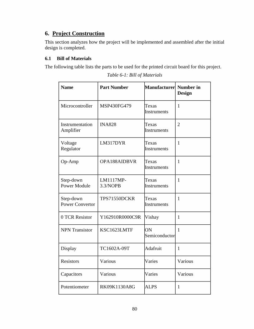
80
6. Project Construction
This section analyzes how the project will be implemented and assembled after the initial
design is completed.
6.1 Bill of Materials
The following table lists the parts to be used for the printed circuit board for this project.
Table 6-1: Bill of Materials
Name Part Number Manufacturer Number in
Design
Microcontroller MSP430FG479 Texas
Instruments
1
Instrumentation
Amplifier
INA828 Texas
Instruments
2
Voltage
Regulator
LM317DYR Texas
Instruments
1
Op-Amp OPA188AIDBVR Texas
Instruments
1
Step-down
Power Module
LM1117MP-
3.3/NOPB
Texas
Instruments
1
Step-down
Power Convertor
TPS71550DCKR Texas
Instruments
1
0 TCR Resistor Y162910R0000C9R Vishay 1
NPN Transistor KSC1623LMTF ON
Semiconductor
1
Display TC1602A-09T Adafruit 1
Resistors Various Varies Various
Capacitors Various Varies Various
Potentiometer RK09K1130A8G ALPS 1

81
Buttons SKQGADE010 ALPS 5
Input/Output
connectors
Various Varies 3
LEDs Various Varies 2
Voltage
reference
LM4040B30IDBZR Texas
Instruments
1
PN Diodes MMDL6050T1G ON
Semiconductor
2
Schottky Diodes CDBH0230-G Comchip 5
Relay G6K-2F-Y_DC3 Omicron 1
6.2 Resonator Testing
This section elaborates on the testing specific to the resonator.
6.2.1 Setup
To characterize the initial response of the resonator to current and temperature stimuli, the
portion of a wafer containing the resonator was glued to a portion of a silicon wafer using
thermal paste. The thermal paste allows the heat from the chamber chuck to transfer to the
die.
Figure 6-1: Resonator sample adhered to portion of silicon wafer
Then, a portion of a copper breadboard had pins soldered to it and was also glued to a
portion of a silicon wafer using an adhesive. The pins were soldered on in order to provide

82
easier access for reading the voltage and/or current associated with the resonator under
certain conditions. Without these pins, connecting a multimeter or measurement device to
read the voltage across or current through the resonator would be cumbersome.
Figure 6-2: Breadboard with soldered pins on silicon
This portion of the silicon wafer was also glued to the same wafer as the die. They were
placed close together so that wire bonding could be done as easily as possible. The
resonator was usually bonded to the copper pads closest to the edge of the breadboard; as
the wire bonding was completed many times over, it became more and more apparent that
the angle at which the two bonds were completed was important. For instance, a bond
completed as shown below on the left is not good because the second one is at an angle
compared to the first bond. In contrast, on the right, the second bond is exactly 90° north
of the first bond. When the bonds are not made at the proper angle, stresses on the first
bond are often greater than the force adhering the bond to the copper breadboard, and the
first bond will lift off of the substrate. Hence, the second bond must be 90° north of the
first, even if this means rotating the setup to make this feasible.
Figure 6-3: Example of bad (left) and good (right) first and second bond location

83
Figure 6-4: Wafer portion with resonator sample and breadboard
The above figure shows the final testing setup just prior to the wire bonding between the
die and the breadboard. The following image depicts the (from left to right) the breadboard
with soldered pins, sample of the wafer containing the resonators, and the wire bonder
needle. This is before the resonator has been bonded to the breadboard.
Figure 6-5: Actual setup of resonator testing
Figure 6-6 depicts the final testing setup after wire bonding is complete. Then, an
ohmmeter or voltage source can be attached to connector pins to obtain a better
understanding of the electrical characteristics of the resonator.

84
Figure 6-6: Final testing setup
6.2.2 Wire Bonding
The breadboard rows connected to each pin were each connected to a side of the resonator
using aluminum wire from an ultrasonic wire bonder. Aluminum wire was chosen because
of its low cost and the low temperature at which it can be used. The bonder used was the
West-Bond 7400A. This is an ultrasonic wire bonder that is used at room temperature. It
was used for this experiment to make wedge bonds. Essentially, there is a bit of wire that
protrudes from the needle and is melted into a sphere using ultrasonic energy. The first ball
is deposited in such a way that the aluminum wire does not break; thus, the needle can be
moved to another place for the second ball to be deposited. After this, the wire in the needle
snaps, and the user is left with a wire bonded in two places on the substrate [41].
Figure 6-7: Sample of wire bonding activity
For both depositions, the wire bonder is activated by pressing the needle into the substrate.
The user-controlled variables on the machine are time and power, and the user also has
control over the speed and force with which the needle is moved and placed on the
substrate.
Using this wire bonder takes skill and experience. There are a number of aspects of
operation that have to be done in a particular manner, or else the bonds will not hold.
Descriptions, pictures, and instructions are no substitute for experience on this machine.
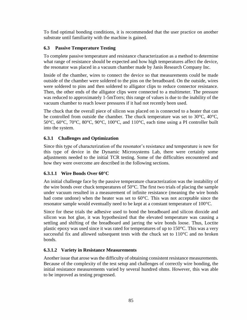
85
To find optimal bonding conditions, it is recommended that the user practice on another
substrate until familiarity with the machine is gained.
6.3 Passive Temperature Testing
To complete passive temperature and resistance characterization as a method to determine
what range of resistance should be expected and how high temperatures affect the device,
the resonator was placed in a vacuum chamber made by Janis Research Company Inc.
Inside of the chamber, wires to connect the device so that measurements could be made
outside of the chamber were soldered to the pins on the breadboard. On the outside, wires
were soldered to pins and then soldered to alligator clips to reduce connector resistance.
Then, the other ends of the alligator clips were connected to a multimeter. The pressure
was reduced to approximately 1-5mTorrs; this range of values is due to the inability of the
vacuum chamber to reach lower pressures if it had not recently been used.
The chuck that the overall piece of silicon was placed on is connected to a heater that can
be controlled from outside the chamber. The chuck temperature was set to 30°C, 40°C,
50°C, 60°C, 70°C, 80°C, 90°C, 100°C, and 110°C, each time using a PI controller built
into the system.
6.3.1 Challenges and Optimization
Since this type of characterization of the resonator’s resistance and temperature is new for
this type of device in the Dynamic Microsystems Lab, there were certainly some
adjustments needed to the initial TCR testing. Some of the difficulties encountered and
how they were overcome are described in the following sections.
6.3.1.1 Wire Bonds Over 60°C
An initial challenge face by the passive temperature characterization was the instability of
the wire bonds over chuck temperatures of 50°C. The first two trials of placing the sample
under vacuum resulted in a measurement of infinite resistance (meaning the wire bonds
had come undone) when the heater was set to 60°C. This was not acceptable since the
resonator sample would eventually need to be kept at a constant temperature of 100°C.
Since for these trials the adhesive used to bond the breadboard and silicon dioxide and
silicon was hot glue, it was hypothesized that the elevated temperature was causing a
settling and shifting of the breadboard and jarring the wire bonds loose. Thus, Loctite
plastic epoxy was used since it was rated for temperatures of up to 150°C. This was a very
successful fix and allowed subsequent tests with the chuck set to 110°C and no broken
bonds.
6.3.1.2 Variety in Resistance Measurements
Another issue that arose was the difficulty of obtaining consistent resistance measurements.
Because of the complexity of the test setup and challenges of correctly wire bonding, the
initial resistance measurements varied by several hundred ohms. However, this was able
to be improved as testing progressed.
86
6.4 Characterization Results
Characterization of the TCR was determined to be unnecessary for this project, as each
resonator that the user wanted to stabilize would need to have its TCR measured and
adjusted in the code. The resistance will be controlled instead of the temperature because
of the convenience. This will be effective because of the close correlation between
temperature and resistance.
6.5 Project Testing and Prototype Construction
The purpose of the prototyping stage is to create a testable model that meets project
requirements and will allow for replication or improvements from. This is crucial in the
design process because it will allow the current design to be evaluated and further
prioritized. Furthermore, it will clarify the production process and identify costs and issues.
These tests will be performed on the both the hardware and software components of this
project to ensure full functionality and addressment of any faults.
6.5.1 Resistor Testing
Initially, the final printed circuit board will not be tested on a resonator; it will be tested on
a resistor. The two pads for wire bonding the resonator will have a resistor soldered to
them. Since resistors do change value with temperature, the resistor’s datasheet can be
referred to for an examination of the effectiveness of the circuit. However, the resistor
should not exhibit resonance, so testing the frequency stability will be more difficult in this
stage. This step will mostly test the voltage and current and their regulation. A resonator
will not be used in this step because one of the requirements of the circuit is that it be
failsafe. However, this cannot be ascertained until the overall operation of the PCB has
been tested. Thus, a resistor will be used in place of the resonator for initial testing.
6.5.2 Resonator Testing
When the circuit has been deemed failsafe and properly functional, a resonator will be wire
bonded to the connection pads. Then, operation and performance of the resonator can be
examined both in terms of resistance and resonance frequency. A bench supply will be
used to power the circuit. The resistance should be shown to the user on the display.
6.5.3 Demonstration
The circuit board is designed to be powered using a bench supply and thus can be
demonstrated in any indoor setting with access to a wall plug to power the bunch supply.
Prior to the demonstration, a resonator or resistor will need to be connected to the pads for
resistance measurements. This can be done through wire bonding for a resonator and
soldering for a resistor. The power supply will need to be set to 10V and activated. The
user will need to set the desired temperature for the resonator. The output for user
edification should be displayed on the LCD screen. Once the desired temperature and
setpoint have been reached, the circuit should operate at that temperature and resistance
with little deviation. This can be verified by user observation.

87
6.5.4 Software Testing
The evaluation of the software is critical for verifying the correct performance of the
application. This software component of this system will need to be able to power on,
receive voltage and current inputs and perform calculations and conversions based on the
input. Furthermore, the processor will need to be able to properly present the resistance
and temperature measurements to the LCD screen, and the microcontroller will need to be
able to produce a new voltage value based on the given inputs to send back to the resonator.
Also, it would be advantageous if the microcontroller had the capability to display error
messages to the LCD screen once common errors are determined.
Objective: The objective of this test is to verify that the software component of this project
is satisfying requirements and functioning as programmed.
Environment: The chosen environment for testing and prototyping is the designated
Senior Design Laboratory in the Engineering II Building, Room 456 at UCF. Personal
computers with Code Composer Studio will be used to modify the code while testing.
Procedure: The following steps will be implemented in order to test the functionality of
the software component of this project.
1. Turn on the processor and anticipate for the LCD screen to properly display the test
message. The display should read the word “Testing”.
2. Verify that the display clears itself and configures the resistance to be displayed on
the first line of the LCD screen.
3. The display should now read the measurement phrase “Resistance = […]”
4. Compare the manually measured resistance with the resistance displayed on the
LCD screen.
5. Convert this resistance to the corresponding temperature using the given lookup
table and toggle the reading on the LCD screen by clicking the button on the
microcontroller.
6. Verify that the display clears itself and configures the temperature to be displayed
on the first line of the LCD screen.
7. The display should now read the measurement phrase “Temperature = […]”
8. Compare the manually determined temperature with the temperature displayed on
the LCD screen.
9. The algorithm will be deemed successful if the resistance and temperatures values
fall within the appropriate level of tolerance. Otherwise, the test will need to be
rerun and there will be possibility for modification of the current code.
Figure 6-8 shows the initial stages of testing with a device from the MSP430 family with
an attached LCD screen.

88
Figure 6-8: MSP430 testing
6.5.5 Microcontroller Power and Protection
The microcontroller is equipped with capacitors connecting the microcontroller voltage
and ground. These help decrease noise and protect the microcontroller.
6.5.6 DC-to-DC Power Testing
In the schematic, two LEDs have been placed that will verify the power levels and traces
running to the microcontroller. They are each accompanied with a series resistor that
ensures the proper voltage is reaching the LED. The formula for calculating the resistor is
given by the following equation:
𝑅𝐿𝐸𝐷 =𝑉𝑠 − 𝑉𝐿𝐸𝐷
𝐼𝐿𝐸𝐷
Vs is the voltage supplied to the LED (in this case, the supply voltage or microcontroller
voltage), while VLED and ILED are given in the datasheet for the LED.
The LED family chosen for this project is the SML-D13x, which has a 20mA typical
forward current and a 2.0V and 2.1V forward voltage for the red and green LEDs,
respectively.
The green LED is activated when the display voltage is at 3.3V. Thus, the resistor for the
green LED should be 60Ω. The red LED is activated when the display voltage is at 5V.
Thus, the resistor for the red LED should be 150Ω.
6.5.7 Operational-Amplifier Circuit Testing
Within the project schematic design, there are two operational-amplifier sections that are
used to amplify or decrease voltage to ensure that it is within the input voltage range of the
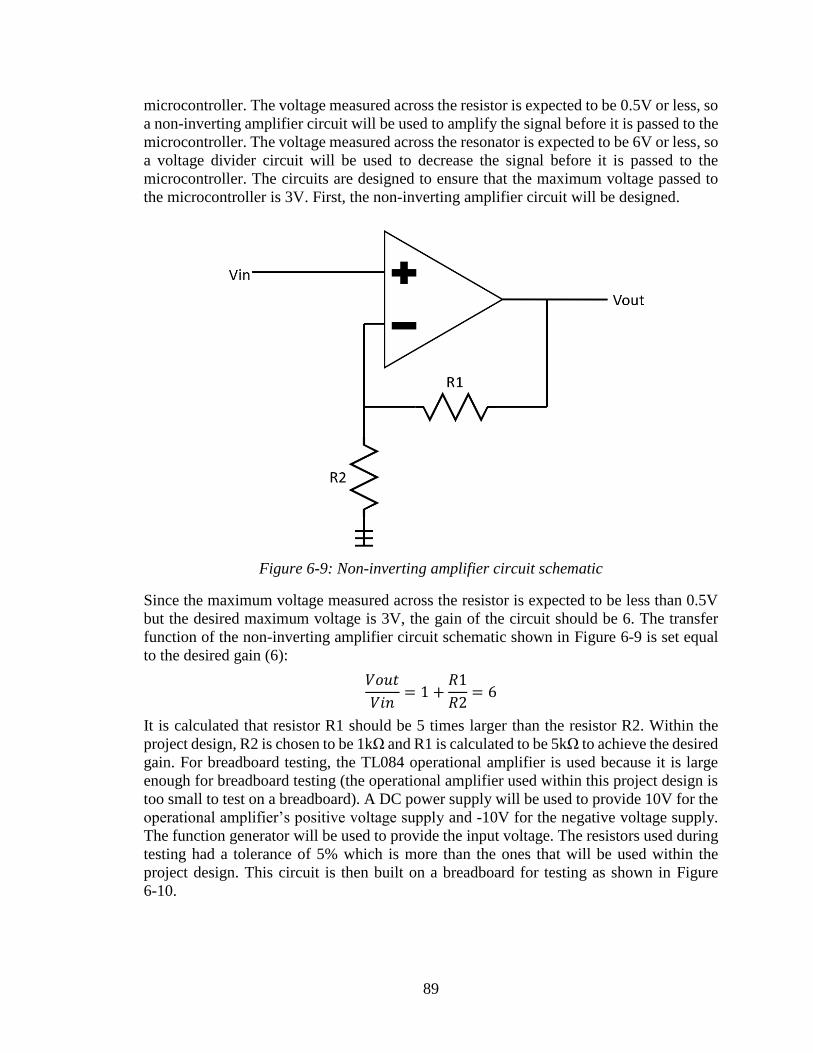
89
microcontroller. The voltage measured across the resistor is expected to be 0.5V or less, so
a non-inverting amplifier circuit will be used to amplify the signal before it is passed to the
microcontroller. The voltage measured across the resonator is expected to be 6V or less, so
a voltage divider circuit will be used to decrease the signal before it is passed to the
microcontroller. The circuits are designed to ensure that the maximum voltage passed to
the microcontroller is 3V. First, the non-inverting amplifier circuit will be designed.
Figure 6-9: Non-inverting amplifier circuit schematic
Since the maximum voltage measured across the resistor is expected to be less than 0.5V
but the desired maximum voltage is 3V, the gain of the circuit should be 6. The transfer
function of the non-inverting amplifier circuit schematic shown in Figure 6-9 is set equal
to the desired gain (6):
𝑉𝑜𝑢𝑡
𝑉𝑖𝑛= 1 +
𝑅1
𝑅2= 6
It is calculated that resistor R1 should be 5 times larger than the resistor R2. Within the
project design, R2 is chosen to be 1kΩ and R1 is calculated to be 5kΩ to achieve the desired
gain. For breadboard testing, the TL084 operational amplifier is used because it is large
enough for breadboard testing (the operational amplifier used within this project design is
too small to test on a breadboard). A DC power supply will be used to provide 10V for the
operational amplifier’s positive voltage supply and -10V for the negative voltage supply.
The function generator will be used to provide the input voltage. The resistors used during
testing had a tolerance of 5% which is more than the ones that will be used within the
project design. This circuit is then built on a breadboard for testing as shown in Figure
6-10.
90
Figure 6-10: Non-inverting amplifier circuit
To test that this design works for a range of voltage values, the input voltage (Vin) is set to
a low frequency (200Hz) sine wave with a peak-to-peak voltage (Vpp) of 500mV using a
function generator. The oscilloscope is used to measure the input voltage waveform (dark
blue) and output voltage waveform (light blue) as shown in Figure 6-11.
Figure 6-11: Non-inverting amplifier circuit voltage output and input waveforms
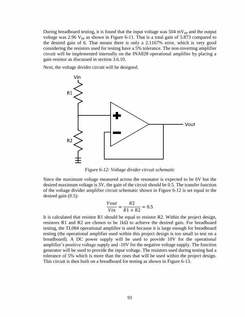
91
During breadboard testing, it is found that the input voltage was 504 mVpp and the output
voltage was 2.96 Vpp as shown in Figure 6-11. That is a total gain of 5.873 compared to
the desired gain of 6. That means there is only a 2.1167% error, which is very good
considering the resistors used for testing have a 5% tolerance. The non-inverting amplifier
circuit will be implemented internally on the INA828 operational amplifier by placing a
gain resistor as discussed in section 3.6.10.
Next, the voltage divider circuit will be designed.
Figure 6-12: Voltage divider circuit schematic
Since the maximum voltage measured across the resonator is expected to be 6V but the
desired maximum voltage is 3V, the gain of the circuit should be 0.5. The transfer function
of the voltage divider amplifier circuit schematic shown in Figure 6-12 is set equal to the
desired gain (0.5):
𝑉𝑜𝑢𝑡
𝑉𝑖𝑛=
𝑅2
𝑅1 + 𝑅2= 0.5
It is calculated that resistor R1 should be equal to resistor R2. Within the project design,
resistors R1 and R2 are chosen to be 1kΩ to achieve the desired gain. For breadboard
testing, the TL084 operational amplifier is used because it is large enough for breadboard
testing (the operational amplifier used within this project design is too small to test on a
breadboard). A DC power supply will be used to provide 10V for the operational
amplifier’s positive voltage supply and -10V for the negative voltage supply. The function
generator will be used to provide the input voltage. The resistors used during testing had a
tolerance of 5% which is more than the ones that will be used within the project design.
This circuit is then built on a breadboard for testing as shown in Figure 6-13.

92
Figure 6-13: Voltage divider circuit
To test that this design works for a range of voltage values, the input voltage (Vin) is set to
a low frequency (200Hz) sine wave with a peak-to-peak voltage of 1V using a function
generator. The oscilloscope is used to measure the input voltage waveform (dark blue) and
output voltage waveform (light blue) as shown in Figure 6-14.
Figure 6-14: Voltage divider circuit voltage output and input waveforms
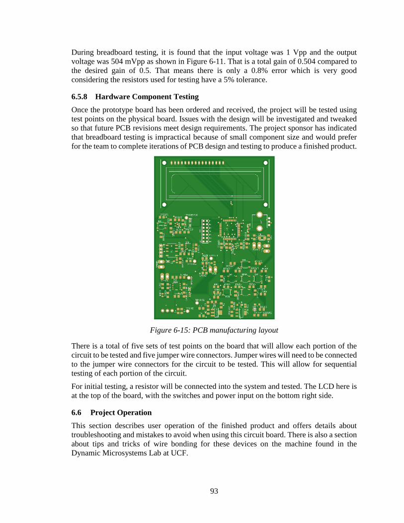
93
During breadboard testing, it is found that the input voltage was 1 Vpp and the output
voltage was 504 mVpp as shown in Figure 6-11. That is a total gain of 0.504 compared to
the desired gain of 0.5. That means there is only a 0.8% error which is very good
considering the resistors used for testing have a 5% tolerance.
6.5.8 Hardware Component Testing
Once the prototype board has been ordered and received, the project will be tested using
test points on the physical board. Issues with the design will be investigated and tweaked
so that future PCB revisions meet design requirements. The project sponsor has indicated
that breadboard testing is impractical because of small component size and would prefer
for the team to complete iterations of PCB design and testing to produce a finished product.
Figure 6-15: PCB manufacturing layout
There is a total of five sets of test points on the board that will allow each portion of the
circuit to be tested and five jumper wire connectors. Jumper wires will need to be connected
to the jumper wire connectors for the circuit to be tested. This will allow for sequential
testing of each portion of the circuit.
For initial testing, a resistor will be connected into the system and tested. The LCD here is
at the top of the board, with the switches and power input on the bottom right side.
6.6 Project Operation
This section describes user operation of the finished product and offers details about
troubleshooting and mistakes to avoid when using this circuit board. There is also a section
about tips and tricks of wire bonding for these devices on the machine found in the
Dynamic Microsystems Lab at UCF.
94
6.6.1 Wire Bonding Tips
Before practicing on the actual resonator sample, be sure to practice with another device
first. Particularly for manual wire bonders, there will be a learning curve as the proper
power and time are set and as the machine is correctly threaded and operated. The wire
bonder used for testing this device has to have the wire at exactly the right place between
the clamps. This could be adjusted by increasing or decreasing the needle height. Ensure
that the power supply and the machine are one the same bond number (1 or 2) each time.
If the bonds are not sticking, ensure that the sample’s substrate is well adhered to whatever
stage is being used. If using tape or glue, try applying a new layer. If the substrate is not
well adhered to the stage, the vibrations from the ultrasonic bonding process will cause the
substrate to vibrate and not be as stable of a medium for bonding.
Power optimization is also very crucial, as too little or too much power can also cause the
bonds to not adhere to the sample or the connector. Often, this range can also be very
narrow; sometimes, changing the power by five can mean the difference between a strong
and weak bond. Thus, trial and error and research must be carried out to find the best power
and time settings for that particular substrate.
For the West-Bond 7400A used for these experiments, if the needle cannot be threaded
because the wire keeps curling, the needle is potentially jammed. Its threading hole can be
examined for a jam under a microscope. If there is indeed a piece of wire wedged into the
needle and blocking it from being threaded, the needle can either be soaked in acetone to
unclog it or must simply be replaced.
7. User Manual
7.1 Hardware
This section discusses the hardware of the project that relates to the user.
7.1.1 User interface
Switches:
Most of the switches for the user interface are arranged in the following manner on the
bottom right side of the board:
SW2
SW1 ENTER SW3
MODE SW4 switch
SW1 represents “Left”, SW2 is “Up”, SW3 is “Right”, and SW4 is “Down”. These are
used for setting the desired value (of current or resistance, depending on the mode). MODE
is used to toggle modes and can be held down at any point to bring the user to the main
menu. ENTER confirms a user decision.

95
Figure 7-1: Button layout on PCB
The RST button is the reset button, and this restarts the program. It is separate from the rest
of the buttons (to prevent accidental resetting) and is located in the top left of board.
SW 5
Potentiometer:
The potentiometer in the upper right near the LCD is for contrast control for the LCD.
Turning it will brighten or dim the characters on the display.
Figure 7-2: Potentiometer on PCB
Power input:
The power is connected to the circuit using a screw terminal in the front left of the board.
The terminal labeled with a ‘-’ should be connected to -10V, the ‘+’ terminal should be
connected to +10V, and the ‘ ’ goes to ground.
Figure 7-3: Screw terminal on PCB
JTAG Connector:
The microcontroller programming interface is connected from a computer using the MSP-
FET430UIF. The JTAG connector connects as shown in the figure below, with the tabbed
side aligned with the ‘[’ on the PCB.
Figure 7-4: JTAG interface on PCB

96
7.1.2 PCB Layout
The PCB layout is modular in design, such that each portion from the schematic is grouped
together on the board. This section details what each of the section on the board are. Test
points (which have been soldered together) initially separated each portion of the circuit
for debugging purposes.
Figure 7-5: Populated PCB
7.1.3 Reset Button
Section A is the reset button and its associated resistor and capacitor. The following
schematic corresponds to this section:
Figure 7-6: Reset button schematic
The RST button is the reset button, and this restarts the program. It is separate from the rest
of the buttons (to prevent accidental resetting) and is in the top left of board.
A B
C D
E
F
G
H
K
M L
N O P Q
I
J
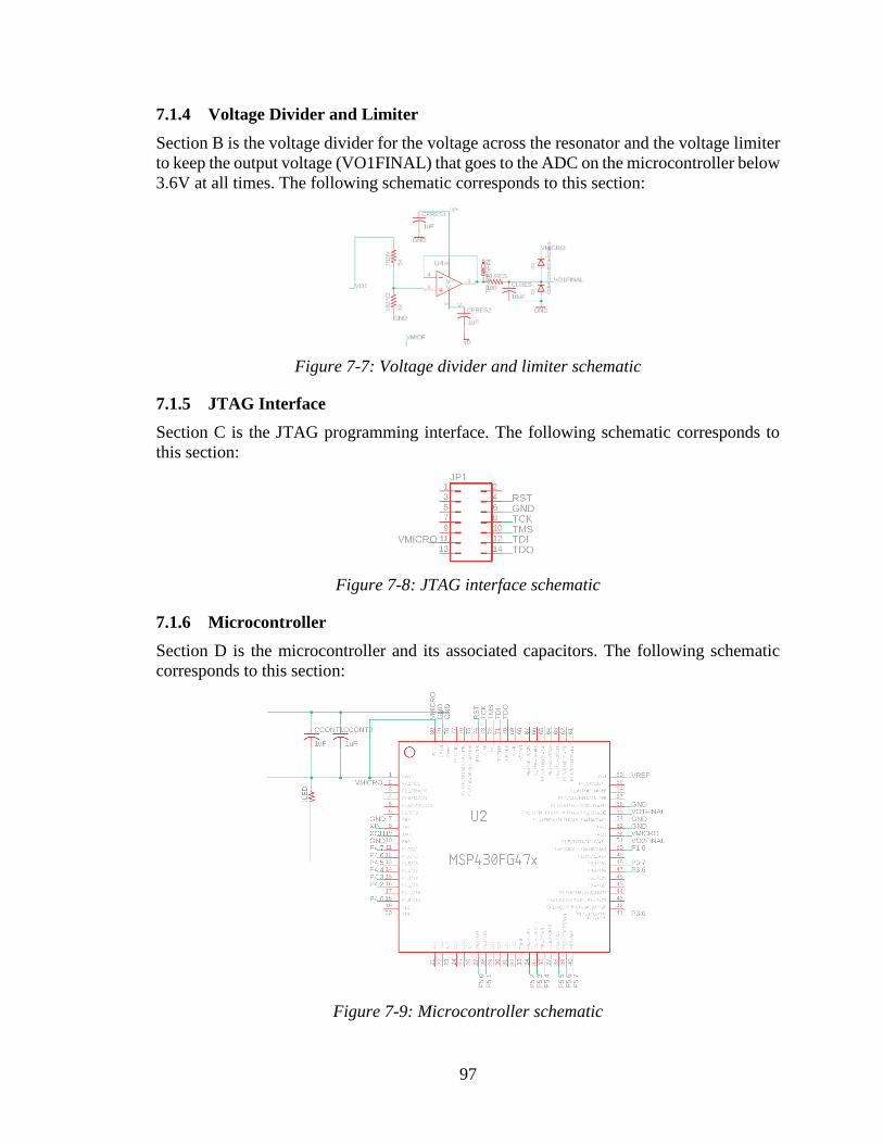
97
7.1.4 Voltage Divider and Limiter
Section B is the voltage divider for the voltage across the resonator and the voltage limiter
to keep the output voltage (VO1FINAL) that goes to the ADC on the microcontroller below
3.6V at all times. The following schematic corresponds to this section:
Figure 7-7: Voltage divider and limiter schematic
7.1.5 JTAG Interface
Section C is the JTAG programming interface. The following schematic corresponds to
this section:
Figure 7-8: JTAG interface schematic
7.1.6 Microcontroller
Section D is the microcontroller and its associated capacitors. The following schematic
corresponds to this section:
Figure 7-9: Microcontroller schematic

98
The following table describes the connections to the microcontroller and their function.
Table 2: Microcontroller connections
Pin Number Pin Name Connection Function in Design
1 DVcc1 VMICRO Digital supply voltage, positive
terminal
7 GND Ground pin Ground pin
8 XIN Crystal in Optional external oscillator
connected via test pins
9 XOUT Crystal out Optional external oscillator
connected via test pins
10 GND Ground pin Ground pin
12 P4.6 SW4 Switch Four
13 P4.5 SW3 Switch Three
14 P4.4 SW2 Switch Two
15 P4.3 SW1 Switch One
18 P4.0 LCD RS Selects instruction or data
register
27 P5.0 LCD D0 First LCD data line
28 P5.1 LCD D1 Second LCD data line
34 P5.2 LCD D2 Third LCD data line
35 P5.3 LCD D3 Fourth LCD data line
36 P5.4 LCD D4 Fifth LCD data line
38 P5.5 LCD D5 Sixth LCD data line
39 P5.6 LCD D6 Seventh LCD data line
40 P5.7 LCD D7 Eighth LCD data line
41 P3.0 Relay Controls relay operation
47 P3.6 LCD E Starts data read/write
48 P3.7 LCD RW Selects read or write
50 P1.6 P1.6 DAC, inputs voltage to VCC for
current control
51 P1.5 VO2FINAL SD16 positive analog input A3
52 AVcc VMICRO Analog supply voltage,
positive terminal
53 AVss GND Analog supply voltage,
negative terminal
54 P1.4 GND SD16 negative analog input
A3
55 P1.3 VO1FINAL SD16 positive analog input A4
56 P1.2 GND SD16 negative analog input
A4
60 Vref Vref External reference voltage
70 TDO/TDI TDO Test data output port,
programming data input
terminal

99
71 TDI/TCLK TDI Test data input or test clock
input
72 TMS TMS Test mode select, input port for
device programming and test
73 TCK TCK Test clock (JTAG). TCK is the
clock input port
74 RST/NMI RST Reset input, will be connected
to toggle switch
78 DVss2 GND Digital supply voltage,
negative terminal
79 DVss1 GND Digital supply voltage,
negative terminal
80 DVcc2 VMICRO Digital supply voltage, positive
terminal
7.1.7 Potentiometer
Section E is the potentiometer and its associated resistor and diodes. The diodes are in place
to provide -1.4V to allow the potentiometer to provide the LCD a contrast range of 3.3V
to -1.4V. Note that the value of RLRS1 is actually around 4kΩ on the PCB. The following
schematic corresponds to this section:
Figure 7-10: Potentiometer schematic
7.1.8 Resonator Connector
Section F is the resonator connector. This board uses four-wire connections to eliminate
resistance of the leads. Thus, Terminals 1 and 4 are for the current to flow through while
Terminals 2 and 3 are what the instrumentation amplifier measures the voltage across. The
following schematic corresponds to this section:
Figure 7-11: Resonator connector schematic

100
7.1.9 Relay
Section G is the relay and its associated diode, resistor, and transistor. The following
schematic corresponds to this section:
Figure 7-12: Relay schematic
7.1.10 Instrumentation Amplifier for Resonator
Section H is the instrumentation amplifier and its associated resistors and capacitors. This
would measure the voltage across the resonator. The following schematic corresponds to
this section:
Figure 7-13: Instrumentation amplifier for resonator schematic
7.1.11 Voltage Reference Source
Section I is the external voltage reference and its capacitors, as well as the capacitors for
the microcontroller. The following schematic corresponds to this section:
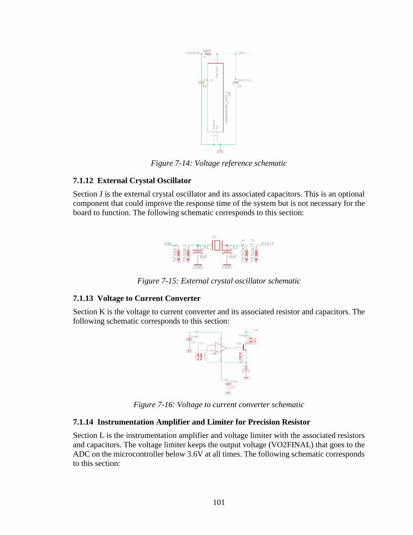
101
Figure 7-14: Voltage reference schematic
7.1.12 External Crystal Oscillator
Section J is the external crystal oscillator and its associated capacitors. This is an optional
component that could improve the response time of the system but is not necessary for the
board to function. The following schematic corresponds to this section:
Figure 7-15: External crystal oscillator schematic
7.1.13 Voltage to Current Converter
Section K is the voltage to current converter and its associated resistor and capacitors. The
following schematic corresponds to this section:
Figure 7-16: Voltage to current converter schematic
7.1.14 Instrumentation Amplifier and Limiter for Precision Resistor
Section L is the instrumentation amplifier and voltage limiter with the associated resistors
and capacitors. The voltage limiter keeps the output voltage (VO2FINAL) that goes to the
ADC on the microcontroller below 3.6V at all times. The following schematic corresponds
to this section:

102
Figure 7-17: Instrumentation amplifier for precision resistor schematic
7.1.15 Buttons
Section M is the user interface buttons (except the reset button, which is in the top left
corner of the board) and their associated resistor and capacitor. The following schematic
corresponds to this section:
Figure 7-18: Buttons schematic
7.1.16 Screw Terminal
Section N is the screw terminal. The following schematic corresponds to this section:
Figure 7-19: Screw terminal schematic
7.1.17 Adjustable Voltage Regulator
Section O is the adjustable voltage regulator and its associated resistors and capacitors. See
the Design Optimization: Section A for more information about the equation for VREG.
The following schematic corresponds to this section:

103
Figure 7-20: Adjustable voltage regulator schematic
7.1.18 3.3V Voltage Regulator
Section P is the 3.3V voltage regulator to power the microcontroller and its associated
capacitors. The following schematic corresponds to this section:
Figure 7-21: 3.3V voltage regulator schematic
7.1.19 5V Voltage Regulator
Section Q is the 5V voltage regulator to power the LCD and its associated capacitors. The
following schematic corresponds to this section:
Figure 7-22: 5V voltage regulator schematic
7.2 Operation
This section details the operation of the board, first going through the start up process, then
describing each mode, and user errors.

104
7.2.1 Start-Up
This section describes the operation of the circuit as the system starts up and displays,
“Running checks…” on the LCD.
To check if the initial current set by the system is actually within range, the first step of the
program is to short-circuit the resonator to ensure the default outputted current value is
acceptable before any current is passed through the resonator. Thus, the relay will click
shut, and the system will perform a self-check on the current.
The voltage across the 10Ω resistor will be measured, and if the value is within a certain
range, the relay will open, and current will then be forced to pass through the resonator.
Otherwise, it will stay closed to protect the resonator from having an unexpected current
pass through it.
To test if the device has a positive or negative TCR (temperature coefficient of resistance),
the system outputs a certain current value and stores the resistance value. It then outputs a
slightly larger current value and measure the resistance value of the resonator again,
subtracting the two to see if the resistance of the device increases or decreases with
increasing current.
To select a mode, the user pushes “MODE” to toggle modes and then presses enter to select
the desired mode.
7.2.2 Modes
Standby Mode:
The standby mode limits the program loop to read relevant resistor values and output the
calculated resistance to the LCD screen.
Operational Mode:
The operational mode allows the user to input the desired resistance value for the program
to stabilize the resistor at and performs the necessary calculations to determine the current
for the next iteration of the loop. The operational mode continues to calculate the resistance
and current to display to the user throughout the process.
Characterization Mode:
The characterization mode allows the user to input a desired current value for the circuit to
operate at and then continuously calculates the resistance and current and output them to
the display.
7.2.3 Errors
This section describes certain errors that the software has been programmed to catch.
No device Hold enter when connected:
This error will be shown if the user disconnects the resonator at any point while the system
is operational, the program will register this and close the relay so that the instrumentation
amplifier is not trying to read the voltage across an open circuit and drawing lots of current
in the process.

105
To fix this, simply connect a resistor or resonator into the four-terminal connector on the
PCB and hold then hold the “Enter” button until the .
Invalid input:
In Operational Mode, there are certain ranges on the setpoint for the resistance. For a
negative TCR device, the resistor’s resistance cannot be set above the initial resistance
measured. For a positive TCR device, the resistor’s resistance cannot be set below the
initial resistance measured. Thus, a new value of resistance that is within the allowable
range will need to be entered.
Current too high:
In Characterization Mode, the current cannot exceed the maximum current value allowed
by the system. Thus, a new value of current that is within the allowable range will need to
be entered.
Current check failed:
This means that the initial current check performed with the relay closed (to ensure that the
system is outputting the expected current value) has failed. Troubleshooting options for
this error include measuring the exact voltage across the 10Ω resistor to see if the hardware
or software is malfunctioning.
FET not found:
This error occurs when the user is attempting to program the microcontroller, but Code
Composer Studio cannot find the microcontroller. There are a few things that can cause
this error. First, ensure that the board is powered on. Second, make sure the JTAG
connector is plugged into the 2x7 pin connector on the PCB. Third, make sure that the RST
pin is not being pressed. All three of those things will prevent the board from being
programmed.
7.3 Design Optimization
7.3.1 Maximum Current Range
The following image depicts the analog portion of the circuit board design.

106
Figure 7-23: Analog schematic design
The schematic shown above operates in the following manner: A voltage (Vin) is input to
U8, which is a precision op-amp, from the microcontroller, and this voltage is converted
to a current according to the following equation:
𝐼𝑠𝑒𝑡 = 𝑉𝑖𝑛
𝑅𝑠𝑒𝑡
Because of the NPN transistor (Q1), the current through Rmea and Rres should now equal
𝛽
(𝛽 + 1)𝐼𝑠𝑒𝑡 = 𝐼𝑟𝑒𝑠 = 𝐼𝑚𝑒𝑎
With a sufficiently large β, Iset approximately equals Ires and Imea. The voltage regulator
source helps keep a stable voltage across the resonator so that there is always enough
voltage to be dropped across Rmea, the resonator, the transistor, and Rset, even when the set
current is operating at its highest allowable value.
The first order filters across the instrumentation amplifiers help filter noise from the
resonator and Rmea. These instrumentation amplifiers measure the voltage across the
resonator and Rmea. These values are then passed into the microcontroller and used to
calculate the resistance of the resonator.
The maximum voltage input (Vin) is Vref/2. Thus, the current limit provided by the
microcontroller is
𝐼𝑚𝑖𝑐𝑟𝑜𝐿𝑖𝑚𝑖𝑡 = (𝑉𝑟𝑒𝑓/2)
𝑅𝑠𝑒𝑡
Additionally, the maximum current is also limited by the following equation:
Vreg - Iset(Rset + Rmea + Rres) – VBJT >0

107
where Vreg = 1.25V*𝑅1+ 𝑅2
𝑅2, and VBJT = VCE(sat) = 0.3V according to the datasheet. The code
checks both limits before it outputs a voltage to the VCC that exceeds these limits. Thus,
adjusting Vreg, Rset, Rmea, Rres, and VBJT will allow for adjustment of the allowable current
range.

108
8. Personnel and Administrative Content
This section discusses all personnel contributing to this project, financing, and any other
administrative content related to this project.
8.1 Project Responsibilities
The project roles and responsibilities of each member are detailed in this section. The group
consists of three members: two electrical engineers and one computer engineer. The main
priorities consist of schematic design, PCB design and software design and are assigned as
shown in the chart and explained in the paragraphs below it.
Table 8-1: Project Responsibilities
Team Member
Tasks Megan Heather Michaela
Team Coordination
P
Resonator Testing
P
Overall Schematic S P
PCB Schematic Design P S
PCB Board Design S P
PCB Assembly/ Soldering P P
Power Supplies P
Control System Design P S S
Display and User Input
S P
Microcontroller Programming
P
Component Selection P P P
Key: P=Primary, S=Secondary
Megan Driggers will take responsibility for the PID controller design, PCB design, and
setup of the power supplies. She has prior experience working to design a PCB using
AutoCAD Eagle and Texas Instrument’s WEBENCH power designer software in the
Junior Design class at UCF. She also has experience examining component datasheets and
power requirements from the Electronics II class and lab taught at UCF which will give an
advantage in choosing the best-suited components. Megan has also taken several courses
involving power and systems including fundamentals of power systems, linear control
systems, and digital control systems. This background knowledge will translate directly to
her tasks.
Michaela Pain will be responsible for choosing the microcontroller and its accompanying
accessories to achieve the user-related requirements outlined by Dr. Abdolvand’s research
group. This will include defining the appropriate inputs and outputs for the microcontroller

109
and programming the microcontroller to calculate the necessary values based on the
received input. Michaela Pain has experience with microcontroller programming from the
Digital Systems and Embedded Systems classes offered at UCF. She will be responsible
for any additional software features that are incorporated into the project throughout the
product development lifecycle. As a computer engineering major, she has the most
software experience from classes and internships. Hence, she is the best team member to
focus on the microcontroller and its affiliated information.
Heather Hofstee will design the schematic in LTSpiceXVII and AutoCAD Eagle. In
addition, she will also serve as the project lead. She has done research with Dr. Abdolvand
and his group for the past year, so she is the most familiar with project and its background.
Additionally, she works in the Dynamic Microsystems Lab and is able to ask Dr.
Abdolvand questions related to the project and relay the information to the team. Her
background knowledge of the project and its objective allows her to be able to design the
project schematic with full insight while her experiences with the people involved ensure
that the project keeps moving forward in the right direction.
In addition, all team members will be responsible for testing their designated designs to
achieve a reliable and trusted product. It is encouraged for members to reach out and
communicate regarding any roadblocks encountered during the design and test phases of
the project, especially if the issue is cross-disciplinary. Members will be held accountable
for providing documentation regarding their specific roles to the project. The objective is
to have each member contribute an equivalent amount of documentation towards the
project to promote a fair working environment. This team dynamic will encourage prompt
and quality deliverables.
8.1.1 PCB Design Process Flowchart
Figure 8-1 shows the PCB design process flowchart which breakdowns the work into
discrete milestones and demonstrates the order in which activities need to be completed.
Figure 8-1: PCB design process flowchart
By following this PCB design process, the project was completed through 3 PCB board
iterations. After each iteration, the board was tested and mistakes were evaluated. This
allowed for the process to be repeated and improved every time.
8.1.2 Software Flowchart
Figure 8-2 shows the software flow diagram which details the software logic to be
implemented to achieve the project objectives. In addition, it communicates the intended
functionality of the microcontroller.

110
Figure 8-2: Software flow diagram
8.2 Financing
The financing for this project will be provided by the project sponsor, Dr. Reza Abdolvand.
The projected overall budget for this project is estimated to be $500. After further research
and compilation of the potential parts, it is evident that approximately half of the budget
can be allotted to equipment such as the microcontroller and display and the PCB boards.
This is beneficial since the remaining funds will be reserved for the order of miscellaneous
parts due to unpremeditated decisions and changes regarding the design.

111
Table 8-2: Project Budget
Part Manufacturer Part
Number
Quantity Estimated
Cost
Microcontroller Texas
Instruments
MSP430 4 $9.99
PCB Boards Element 14 N/A 3 $100
Display Adafruit TC1602A-
09T
1 $9.95
Miscellaneous parts for
resonator
N/A N/A N/A $80
Miscellaneous parts for DC
to DC conversions and power
supply
N/A N/A N/A $25
Miscellaneous Parts for
measuring voltage
N/A N/A N/A $30
Shipping Costs
$100
Estimated Total Cost: $384.94, Remaining: $615.06
The budget chart illustrated above shows the specific parts that will be ordered for intended
use in the project. The goal is to remain below budget throughout the duration of the project
in order to simulate real-world experience of project management and budget planning.
The following table lists the finalized project expenses. The project is still well under the
overall ceiling of $1000.

112
Table 8-3: Project Expenses
Expense Vendor Cost (including shipping)
PCB Revision 1 (Quantity: 2) Advanced Circuits $89.77
Parts Digikey $43.77
Parts Mouser $89.64
PCB Revision 2 (Quantity: 1) Advanced Circuits $122.61
Parts Mouser $86.08
Parts Mouser $85.39
PCB Revision 3 (Quantity: 5) PCBWay $74.00
Total Spent: $591.26 Total budget remaining: $408.74
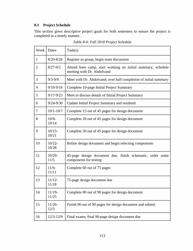
113
8.3 Project Schedule
This section gives descriptive project goals for both semesters to ensure the project is
completed in a timely manner.
Table 8-4: Fall 2018 Project Schedule
Week Dates Task(s)
1 8/20-8/26 Register as group, begin team discussion
2 8/27-9/2 Attend boot camp, start working on initial summary, schedule
meeting with Dr. Abdolvand
3 9/3-9/9 Meet with Dr. Abdolvand; over half completion of initial summary
4 9/10-9/16 Complete 10-page Initial Project Summary
5 9/17-9/23 Meet to discuss details of Initial Project Summary
6 9/24-9/30 Update Initial Project Summary and resubmit
7 10/1-10/7 Complete 15 out of 45 pages for design document
8 10/8-
10/14
Complete 20 out of 45 pages for design document
9 10/15-
10/21
Complete 30 out of 45 pages for design document
10 10/22-
10/28
Refine design document and begin selecting components
11 10/29-
11/5
45-page design document due, finish schematic, order some
components for testing
12 11/6-
11/11
Complete 60 out of 75 pages
13 11/12-
11/18
75-page design document due
14 11/19-
11/25
Complete 80 out of 90 pages for design document
15 11/26-
12/3
Finish 90 out of 90 pages for design document and submit
16 12/3-12/9 Final exams; final 90-page design document due

114
Table 8-5: Spring 2019 Project Schedule
Week Dates Task(s)
1 1/7-1/13 Reconvene group, plan prototyping, schedule meeting with Dr.
Abdolvand
2 1/14-1/20 Meeting with Dr. Abdolvand, begin to order parts
3 1/21-1/27 Begin prototyping
4 1/28-2/3 Assemble prototype, begin testing
5 2/4-2/10 Continue testing, consider redesign
6 2/11-2/17 Redesign if necessary and reorder parts, schedule meeting with Dr.
Abdolvand
7 2/18-2/24 Meeting with Dr. Abdolvand, reassemble prototype, begin testing
8 2/25-3/3 Continue testing, hone working prototype
9 3/4-3/10 Continue testing, hone working prototype
10 3/11-3/17 Finalize working prototype, assign roles regarding final document
11 3/18-3/25 Work on Final Documentation
12 4/1-4/7 Complete Final Documentation
13 4/8-4/14 Prepare for Final Presentation, Peer Reviews
14 4/15-4/21 Final Presentation, Showcase
15 4/22-4/28 Final Exams

115
9. Conclusion
To complete the first phase of the project, the design and documentation of the design had
to be finished. Relevant constraints and standards were examined, noted, and applied.
Throughout bringing the project to completion, the team learned a number of lessons and
gained insight into the design process and improvements that could be made for the design.
Despite not having any significant experience in soldering, the team was able to learn and
become effective at soldering, using both solder, solder paste, and usually four hands to
complete the task. Throughout the duration of the project, components would initially come
loose and create issues with the system. However, these lessons were not in vain, and the
third revision PCB had no issues with loose components. The modular design of the
components ended up being very aesthetically pleasing and intuitive.
From a design standpoint, there are some things that the team would do differently were
they to repeat this project. Upon further reflection, having more characters on the LCD
would have been useful.
Accomplishing mΩ control with this circuit is a unique design problem that requires a
precise and accurate design. Thus, while the design for this project has been completed,
there remain ways to optimize the system. Next steps for this project include control loop
refinement and increasing the maximum resistance value that can be plugged into the
system by changing some resistance values, including the 10Ω precision resistor to a 5Ω
precision resistor (part number Y16255R00000D9W). Resonator testing is still currently
on hold, with all of the testing described here being done with a resistor to confirm safe
operation for the resonator. However, all tests with the last revision PCB indicate a fully
functional system that can be used to test TPoS resonators under a controlled resistance
(and thus stable temperature value).
Figure 9-1: Final Project PCB
116
10. Appendix A: Nomenclature
AC: Alternating current
BOM: Bill of materials
CPU: Central processing unit
DC: Direct current
DCO: Digitally controlled oscillator
ECE: Electrical and computer engineering
IDE: Integrated development environment
JST: Japan solderless terminal
LCD: Liquid crystal display
LUT: Lookup table
MCU: Microcontroller unit
MEMS: Microelectromechanical systems
MSP: Mixed signal processor
OCXO: Oven-controlled crystal oscillator
PCB: Printed circuit board
PID: Proportional-integral-derivative
RISC: Reduced instruction set computer
RoHS: Restriction of hazardous substances
TCF: Temperature coefficient of frequency
TCR: Temperature coefficient of resistance
TPoS: Thin-film piezoelectric-on-substrate
UCF: University of Central Florida
VCCS: Voltage-controlled current source
Vpp: Peak-to-peak voltage

117
11. References
[1
]
R. Abdolvand et al, "Micromachined Resonators: A Review," 2016.
[2
]
K. Khamoushi, "TEMPERATURE COEFFICIENT OF RESONANT FREQUENCY
(TCF)," [Online]. Available: http://www.students.tut.fi/~khamousk/TCF.htm.
[3
]
J. Charmet, R. Daly, J. Thiruvenkatanath, J. Woodhouse and A. Seshial, "Observations
of modal interaction in lateral bulk acoustic resonators," in Applied Physics Letters,
2014.
[4
]
S. Shahraini, R. Abdolvand and H. Fatemi, "Temperature Coefficient of Frequency in
Silicon-Based Cross-Sectional Quasi Lamé Mode Resonators," in IEEE International
Frequency Control Symposium, Olympic Valley, 2018.
[5
]
Texas Instruments , "MSP430G2x53, MSP430G2x13 Mixed Signal Microcontroller
datasheet (Rev. J)," May 2013. [Online]. Available:
http://www.ti.com/lit/ds/symlink/msp430g2553.pdf. [Accessed 26 October 2018].
[6
]
PC Magazine, "Definition of: transmissive LCD," [Online].
[7
]
Lumex Incorporated, "LCM-X01604DXX," 9 October 1998. [Online].
[8
]
Electronics Assembly, "LCD-Modul 2x8 - 5.01mm," October 2016. [Online].
[9
]
Adafruit, "Data Sheet TC1602A-09T SpecV00," 4 June 2009. [Online]. Available:
https://cdn-shop.adafruit.com/product-files/181/p181.pdf. [Accessed 26 October
2018].
[1
0]
Microtips Technology Inc. , "LIQUID CRYSTAL DISPLAY MODULE MODEL:
NMTC-S20200BMNHSGW-12," 6 September 2017. [Online].
[1
1]
"LCD-20x4Y: 20x4 Liquid Crystal Display with HD44780 driver," 2014. [Online].
[1
2]
Newhaven Display International, "NHD-0216K1Z-FL-YBW Character Liquid Crystal
Display Module," 26 March 2018. [Online].
[1
3]
Renesas, "ISL28533, ISL28534, ISL28535, ISL28633, ISL28634, ISL28635," 13
January 2017. [Online].
[1
4]
Analog Devices, "High Performance, Low Power, Rail-to-Rail Precision
Instrumentation Amplifier," 2015. [Online].
[1
5]
Analog Devices, "Low Noise, Low Gain Drift, G = 2000," 2012. [Online].
[1
6]
Texas Instruments, "INA828 50-µV Offset, 7-nV/√Hz Noise, Low-Power, Precision
Instrumentation Amplifier," January 2018. [Online].

118
[1
7]
Texas Instruments, "INA12x Precision, Low-Power Instrumentation Amplifiers,"
January 2018. [Online].
[1
8]
Texas Instruments, "Low Noise, Low-Distortion Instrumentation Amplifier
Replacement for SSM2017 datasheet (Rev. C)," November 2015. [Online]. Available:
http://www.ti.com/lit/ds/symlink/ina217.pdf. [Accessed 26 October 2018].
[1
9]
Texas Instruments, "LM317 3-Terminal Adjustable Regulator," Texas Instruments,
September 2016. [Online].
[2
0]
ON Semiconductor, "NCP110: Linear Regulator, Low VIN, Low Noise and High
PSRR, 200 mA," Semiconductor Components Industries, LLC, July 2018. [Online].
[2
1]
Maxim Integrated, "MAX15006/MAX15007: 40V, Ultra-Low Quiescent-Current
Linear Regulators in 6-Pin TDFN/8-Pin SO," Maxim Integrated, March 2015.
[Online].
[2
2]
Infineon, "TLS115B0: High Precision Voltage Tracker," Infineon, 13 October 2016.
[Online].
[2
3]
ON Semiconductor, "NCP786A: Wide Input Voltage Range 10mA Ultra-Low Iq, High
PSRR Linear Regulator with Adjustable Output Voltage," Semiconductor Components
Industries, LLC, December 2018. [Online].
[2
4]
Semtech, "TS31023/223: High Input Voltage Linear Regulator," Semtech, 4 April
2016. [Online].
[2
5]
Bourns, "Potentiometers LINEARITY TECHNICAL NOTE," 2017. [Online].
[2
6]
TT Electronics, "Rotary Potentiometer P120 Series," TT Electronics, October 2016.
[Online].
[2
7]
Bourns, "3590 - Precision Potentiometer," November 2017. [Online].
[2
8]
Vishay Spectrol, "7/8" (22.2 mm) Multi Turn Wirewound Potentiometer," 17 May
2018. [Online].
[2
9]
ALPS, "RK09K, RK09D: 9mm Size Insulated Shaft Snap-in Type," ALPS. [Online].
[3
0]
Bourns, "3386 - 3/8 ” Square Trimpot® Trimming Potentiometer," May 2016.
[Online].
[3
1]
CTS Electrocomponents, "Series 284 Data Sheet Precision Potentiometer," 22 March
2013. [Online].
[3
2]
Agilent, "Agilent E3631A Triple Output DC Power Supply," July 2013. [Online].
Available:
https://edisciplinas.usp.br/pluginfile.php/2405092/mod_resource/content/1/Agilent_E

119
3631%20Power%20Supply_Users_Guide%20%284%29.pdf. [Accessed 26 October
2018].
[3
3]
Department of Defense, Environmental Engineering Considerations and Laboratory
Tests, G ed., 2008.
[3
4]
National Institute of Standards and Technology, "Compliance FAQs: RoHS,"
Standards Information Center, 19 December 2017. [Online].
[3
5]
International Electrotechnical Commission, "International Standard IEC 60950-1,"
December 2005. [Online]. Available: https://webstore.iec.ch/preview/info_iec60950-
1%7Bed2.0%7Den_d.pdf.
[3
6]
I. C. Society, IEEE Standard System C Language Reference, New York: The Institute
of Electrical and Electronics Engineers, Inc., 2012.
[3
7]
IEEE, ISO/IEC/IEEE 29199 International Standard, New York: The Institute of
Electrical and Electronics Engineers, Inc., 2015.
[3
8]
ISO/IEC, International Standard ISO/IEC 9899, New York, 2005.
[3
9]
H. Hofstee, "Analog Oven-Control Circuit for a Thin-Film Piezoelectric-On-Substrate
Microelectromechanical Systems Oscillator," Orlando, 2018.
[4
0]
Texas Instruments, "OPA828 Low-Offset, Low-Drift, Low-Noise, 50-MHz, 36-V
JFET-Input Op Amp datasheet," September 2018. [Online]. Available:
http://www.ti.com/lit/ds/symlink/opa828.pdf.
[4
1]
T. Gleditch, H. Hvims, R. Rörgren and J. Vähäkangas, "Chapter A: Wire Bonding,"
2000. [Online].
[4
2]
Texas Instruments, "LMZM23600 36-V, 0.5-A Step-Down DC/DC Power Module in
3.8-mm × 3-mm Package," April 2018. [Online]. Available:
http://www.ti.com/lit/ds/symlink/lmzm23600.pdf?HQS=TI-null-null-mousermode-
df-pf-null-wwe&DCM=yes&ref_url=https%3A%2F%2Fwww.mouser.com%2F.
[4
3]
Texas Instruments, "TPS6217x 3-V to 17-V, 0.5-A Step-Down Converters with DCS-
Control™," May 2017. [Online]. Available:
http://www.ti.com/lit/ds/symlink/tps62173.pdf.

120
12. Permissions

121