Micromachined Integrated 2D Transducers for Ultrasound ...
198
General rights Copyright and moral rights for the publications made accessible in the public portal are retained by the authors and/or other copyright owners and it is a condition of accessing publications that users recognise and abide by the legal requirements associated with these rights. Users may download and print one copy of any publication from the public portal for the purpose of private study or research. You may not further distribute the material or use it for any profit-making activity or commercial gain You may freely distribute the URL identifying the publication in the public portal If you believe that this document breaches copyright please contact us providing details, and we will remove access to the work immediately and investigate your claim. Downloaded from orbit.dtu.dk on: Jul 31, 2022 Micromachined Integrated 2D Transducers for Ultrasound Imaging Havreland, Andreas S. Publication date: 2019 Document Version Publisher's PDF, also known as Version of record Link back to DTU Orbit Citation (APA): Havreland, A. S. (2019). Micromachined Integrated 2D Transducers for Ultrasound Imaging. DTU Health Technology.
-
Upload
khangminh22 -
Category
Documents
-
view
0 -
download
0
Transcript of Micromachined Integrated 2D Transducers for Ultrasound ...

General rights Copyright and moral rights for the publications made accessible in the public portal are retained by the authors and/or other copyright owners and it is a condition of accessing publications that users recognise and abide by the legal requirements associated with these rights.
Users may download and print one copy of any publication from the public portal for the purpose of private study or research.
You may not further distribute the material or use it for any profit-making activity or commercial gain
You may freely distribute the URL identifying the publication in the public portal If you believe that this document breaches copyright please contact us providing details, and we will remove access to the work immediately and investigate your claim.
Downloaded from orbit.dtu.dk on: Jul 31, 2022
Micromachined Integrated 2D Transducers for Ultrasound Imaging
Havreland, Andreas S.
Publication date:2019
Document VersionPublisher's PDF, also known as Version of record
Link back to DTU Orbit
Citation (APA):Havreland, A. S. (2019). Micromachined Integrated 2D Transducers for Ultrasound Imaging. DTU HealthTechnology.

Technical University of Denmark
Ph.D. Thesis
Micromachined Integrated 2DTransducers for Ultrasound Imaging
Author:Andreas S. Havreland
Supervisors:Prof. Erik V. ThomsenProf. Jørgen A. Jensen
14st September 2019
Kgs. Lyngby, Denmark

Cover image: Two row-column addressed ultrasound probes developed inthis work. Photo by Jesper Scheel.
Technical University of DenmarkDepartment of Health TechnologyØrsteds Plads 345C2800 Kgs. LyngbyDENMARKTel: (+45) 4525 5700Fax: (+45) 4588 7762Web: www.healthtech.dtu.dkAuthor e-mail: [email protected]

Preface
This PhD thesis has been submitted to the Technical University of Denmark,in partial fulfillment of the requirements for the degree of Doctor of Philos-ophy. The work has been supervised by Professor Erik Vilain Thomsen andProfessor Jørgen Arendt Jensen. This thesis consists of a recapitulation ofthe research work carried out from September 2016 to September 2019 atDTU Health Tech, Technical University of Denmark.
The MEMS group has conducted research within the field of CapacitiveMicromachined Ultrasonic Transducer (CMUT) for several years, and pro-found knowledge of the CMUT technology was therefore already establishedbefore my project.
Andreas HavrelandKgs. Lyngby, September 2019
iii

iv PREFACE

Summary
Conventional ultrasound imaging produces 2D images of the human body,and these images are today routinely used for diagnostics purposes. The two-dimensi images can efficiently be displayed on a computer screen and are easyto interpret, whereas 3D images are more difficult to interpret but provideadditional information about the imaged objects. The added dimension in a3D image can provide vital information and can be used for new innovativeimaging techniques. However, the complexity of the underlying transducertechnology increases enormously when the imaging capabilities go from 2Dto 3D. New advances in the transducer technology , such as row-columnaddressed arrays, drastically reduce the complexity of ultrasound systemscapable of 3D imaging. The row-column technology reduces the requirednumber of electrical interconnection fromN2 to 2N , whereN is the number ofchannels in the ultrasound system. The main goal of this thesis is to developthe row-column addressed transducer array. The technology of capacitiveMicromachined Ultrasound Transducers (CMUT) is used for the developmentplatform for the row-column arrays due to the high flexibility and desiredimaging properties offered by this technology.
Theoretical analysis of a CMUT is presented in the first part of thesis, in-cluding investigation of the static and dynamic properties. Multiple CMUTfabrication methods are developed, demonstrated, and used to fabricate var-ious row-column arrays of different sizes. The area of row-column addressedarrays can be larger than conventional ultrasound transducers which intro-duces new challenges that has to be addressed. These challenges includedincreased resistance in the electrodes, and a design criterion for sufficientresistance of long row-column elements is derived and experimentally docu-mented.
Two 92+92 4.5 MHz row-column addressed CMUT arrays are assembledinto ultrasound probes. The CMUT probes are electrically characterized,
v

vi SUMMARY
long term stability test during 16 h showed no sign of dielectric chargingand the electromechanical coupling coefficient is estimated to be 18.3%. Theacoustical performance of the probes are characterized and 3D imaging ca-pabilities are demonstrated at a depth of 7 cm in a cyst phantom.

Resume
Ultralydsbilleddannelse bliver rutinemæssigt brugt til diagnosticering i medicinsksammenhæng. Konventionelt er ultralydsbilleder i 2D, hvilket bade gør detnemt at fortolke og afbillede pa en computerskærm, hvorimod 3D-billeder ersværere at fortolke men indeholder mere information om det afbillede objekt.Den ekstra dimension i 3D- billede kan give livsvigtig information og banevejen for nye billedeteknikker. Men kompleksiteten af den bagvedliggendetransducerteknologi stiger voldsomt nar man gar fra 2D til 3D. Den nyesteudvikling af transducerkoncepter, sasom række-søjle adressering, reducererdenne kompleksitet drastisk. Række-søjle-adressering reducerer antallet in-dividuelle elektriske forbindelse fra N2 til 2N , hvor N er antallet af kanaler iultralydssystemet. Hovedfokuset i denne afhandling er at udvikle transduc-ere baseret pa teknologien bag rækkesøjle-adressering. Til at facilitere denneudvikling er teknologien baseret pa kapacitive mikrofremstillet ultalydstrans-ducer (CMUT) valgt som platform. Dette valg er grundet fleksibilitet og denøget billedkvalitet som CMUT teknologien tilbyder.
Den første del af afhandlingen indeholder en teoretisk analyse af en CMUT,som inkluderer en gennemgang af de statiske og dynamiske egenskaber. Deru-dover bliver flere forskellige CMUT fabrikationsmetoder gennemgaet, demon-streret, og brugt til at fabrikere række-søjle adresseret CMUT transducere iforskellige størrelser. Arealet af en række-søjle adresset CMUT kan blive be-tydlig større end konventionelle ultralyds transducere hvilket medfører nogleproblemstilling, der skal handteres i CMUT design processen. Et af disseproblemer er øget elektrisk modstand, og et kriterium for den højeste tilladtemodstand i elektroderne er udledt og eksperimentelt demonstreret i denneafhandling. To 92+92 4.5 MHz MHz række-søjle adresseret CMUT trans-ducere er blevet samlet til en ultralydsprobe, og disse prober er akustiskkarakteriseret og har demonstreret 3D ultralydsbilleddannelse ned til 7 cmdybde pa et cystefantom.
vii

viii RESUME

Acknowledgements
First of all I would like to thank my supervisor Prof. Erik V. Thomsen andmy co-supervisor Prof. Jøregn Arendt Jensen. I have learned many thingsfrom both of you during the past three years on a personal and professionallevel. It has been a great experience for me to participate in the importantresearch you are conducting.
Then I would like thank my colleagues at DTU Health Tech. Thankyou for making my time as a PhD student very joyful. A special thankyou goes to my office mate Martin Lind Ommen for always providing afriendly atmosphere at our office and equally important thank you for all theconstructive professional debates we have had on various subjects. Thanksto all the students that I have supervised, you have been an important partof the CMUT development in the MEMS group.
I would also like to thank our partners at BK Medical and DTU Nanolabfor facilitating the research conducted in this thesis. A proper thank youshould also be given to Jan Bagge for his lessons regarding CMUT electronics.
Last, but not least, a huge thanks goes to my family for the continuoussupport. First and foremost to you Mathilde. Thank you for the endlesssupport and love you have provided.
ix

x ACKNOWLEDGEMENTS

Acronyms
AFM Atomic Force Microscope
ASIC Application Specific Integrated Circuit
BCB BenzoCycloButene
BHF Buffed HydroFluoric acid
BOX Burried OXide
CMP Chemical Mechanical Polishing
CMUT Capacitive Micromachined Ultrasonic Transducer
CT Computed Tomography
CV Capacitance-Voltage
DREM Deposit, Remove, Etch, Mask
DTU The Technical University of Denmark
EFE EigenFunction Expansion
FBW Fractional BandWidth
FORCES Fast Orthogonal Row–Column Electronic Scanning
FPM Fully Populated Matrix
xi

xii Acronyms
FWHM Full Width Half Max
IUS International Ultrasound Symposium
IV Current-Voltage
KOH potassium hydroxide
LOCOS Local oxidation of silicon
LPCVD Low Pressure Chemical Vapour Deposition
MMS Method of Multiple Scales
MR Magnetic Resonance
PCB Printed Circuit Board
PDMS polydimethylsiloxane
PECVD Plasma Enhanced Chemical Vapour Deposition
PMUT Piezoelectric Micromachined Ultrasonic Transducers
PSOI Poly-Silicon-On-Insulator
PZT ceramic material with piezoelectric properties
RCA Row-Column-Addressed
RMS Root mean square
SEM Scanning Electron Microscope
SNR Signal to Noise Ratio
SOI Silicon-On-Insulator
SPM Sparsely Populated Matrix
TOBE Top-Orthogonal-to-Bottom-Electrode

Nomenclature
CMUT array
Atrans Area of transducer surface [m2]
f0 Center frequency [Hz]
L Length of an element [m]
N Number of channels [#]
W Width of an element [m]
Single CMUT cell
A Area of a single CMUT cell [m2]
a Radius of a single CMUT cell [m]
F Force (frequency domain) [N·s]
fRI Force from the radiation impedance (time domain) [N]
g Gap height in CMUT cavity [m]
h Thickness of the CMUT plate [m]
ks Linear spring constant of CMUT [N/m]
m Mass of a single CMUT cell [kg]
U Applied DC bias [V]
xiii

xiv Acronyms
Upi Pull-in voltage [V]
V Velocity of the CMUT plate (frequency domain) [m]
v Velocity of the CMUT plate (time domain) [m/s]
x Displacement of the CMUT plate [m]
Z Radiation impedance (frequency domain) [kg/s]
z Radiation impedance (time domain) [kg/s2]
Material properties
ρm Density of medium [kg/m3]
ρp Density of plate [kg/m3]
% Resistivity [Ω · cm]
cm Speed of sound [m/s]
Other
λ Wavelength [m]
ω Angular frequency [rad]
ε Permittivity [F/m]
Ac Cross-sectional area [m2]
C Capacitance [F]
Fe Electrostatic force [N]
Fs Spring force [N]
k Wave number [m−1]
R Resistance [Ω]
t Time [s]

Contents
Preface iii
Summary v
Resume vii
Acknowledgements ix
Acronyms xii
Nomenclature xii
1 Introduction 11.1 CMUT . . . . . . . . . . . . . . . . . . . . . . . . . . . . . . . 2
1.1.1 CMUT outlook . . . . . . . . . . . . . . . . . . . . . . 51.2 2D ultrasound imaging . . . . . . . . . . . . . . . . . . . . . . 51.3 3D ultrasound imaging . . . . . . . . . . . . . . . . . . . . . . 71.4 Thesis outline . . . . . . . . . . . . . . . . . . . . . . . . . . . 81.5 Publications . . . . . . . . . . . . . . . . . . . . . . . . . . . . 9
2 Theory 112.1 Static model . . . . . . . . . . . . . . . . . . . . . . . . . . . . 12
2.1.1 Lumped model . . . . . . . . . . . . . . . . . . . . . . 122.1.2 Clamped plate . . . . . . . . . . . . . . . . . . . . . . 132.1.3 Approximate solutions . . . . . . . . . . . . . . . . . . 14
2.2 Dynamic model . . . . . . . . . . . . . . . . . . . . . . . . . . 16
xv
xvi CONTENTS
2.2.1 Small ka limit . . . . . . . . . . . . . . . . . . . . . . . 18
2.2.2 Large ka limit . . . . . . . . . . . . . . . . . . . . . . . 23
2.2.3 Full description . . . . . . . . . . . . . . . . . . . . . . 26
2.3 Chapter summery . . . . . . . . . . . . . . . . . . . . . . . . . 27
3 Row-Column-Addressed Arrays 29
3.1 Scaling laws . . . . . . . . . . . . . . . . . . . . . . . . . . . . 30
3.2 Geometry . . . . . . . . . . . . . . . . . . . . . . . . . . . . . 35
3.3 Edge waves . . . . . . . . . . . . . . . . . . . . . . . . . . . . 37
3.4 Silicon substrates for row-column CMUT fabrication . . . . . 39
3.5 Chapter summery . . . . . . . . . . . . . . . . . . . . . . . . . 41
4 CMUT fabrication 43
4.1 Fusion bonding . . . . . . . . . . . . . . . . . . . . . . . . . . 44
4.1.1 Characterization . . . . . . . . . . . . . . . . . . . . . 47
4.2 Polymer bonding . . . . . . . . . . . . . . . . . . . . . . . . . 52
4.2.1 Characterization . . . . . . . . . . . . . . . . . . . . . 54
4.3 Anodic bonding . . . . . . . . . . . . . . . . . . . . . . . . . . 57
4.3.1 Characteriaztion . . . . . . . . . . . . . . . . . . . . . 58
4.4 Combined anodic and fusion bonding . . . . . . . . . . . . . . 62
4.4.1 Rodent one . . . . . . . . . . . . . . . . . . . . . . . . 63
4.4.2 Mask layout . . . . . . . . . . . . . . . . . . . . . . . . 67
4.4.3 Characterization . . . . . . . . . . . . . . . . . . . . . 67
4.5 Poly-Silicon-On-Insulator wafer . . . . . . . . . . . . . . . . . 70
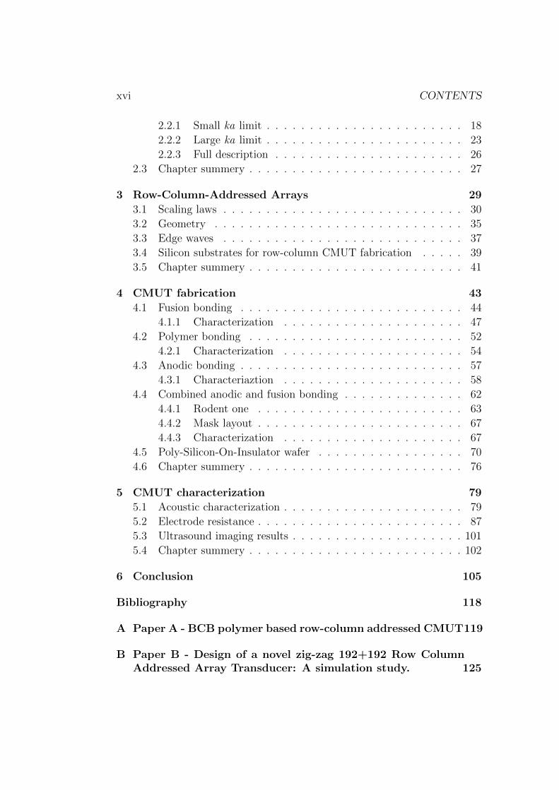
4.6 Chapter summery . . . . . . . . . . . . . . . . . . . . . . . . . 76
5 CMUT characterization 79
5.1 Acoustic characterization . . . . . . . . . . . . . . . . . . . . . 79
5.2 Electrode resistance . . . . . . . . . . . . . . . . . . . . . . . . 87
5.3 Ultrasound imaging results . . . . . . . . . . . . . . . . . . . . 101
5.4 Chapter summery . . . . . . . . . . . . . . . . . . . . . . . . . 102
6 Conclusion 105
Bibliography 118
A Paper A - BCB polymer based row-column addressed CMUT119
B Paper B - Design of a novel zig-zag 192+192 Row ColumnAddressed Array Transducer: A simulation study. 125

CONTENTS xvii
C Paper C - CMUT Electrode Resistance Design: Modelingand Experimental Verification by a Row-Column Array 131
D Paper D - Wafer bonded CMUT technology utilizing Poly-Silicon-on-Insulator wafers 141
E Paper E - A Row-Column-Addressed 2D Probe with andIntegrated Compound Diverging Lens 147
F Fabrication processes 153F.1 LOCOS . . . . . . . . . . . . . . . . . . . . . . . . . . . . . . 153F.2 BCB . . . . . . . . . . . . . . . . . . . . . . . . . . . . . . . . 160F.3 Anodic bond . . . . . . . . . . . . . . . . . . . . . . . . . . . . 165F.4 LOCOS + Anodic bond . . . . . . . . . . . . . . . . . . . . . 171

xviii CONTENTS

CHAPTER 1
Introduction
Medical applications of ultrasound dates back to 1950 [1], and have sincegrown to be a conventional tool for diagnostic purposes. Ultrasound is ad-ditionally routinely used in multiple other applications ranging from parkassist, non destructive testing, fingerprint sensing, gas sensing among other.Ultrasound imaging is like X-ray, Computed Tomography (CT), and Mag-netic Resonance (MR) used to examine the internal part of the human body,and ultrasound imaging has the advantages of offering real time imaging op-posite to the other modalities and additionally at a low cost. However, theresolution of ultrasound imaging is in general inferior compared to the threeother imaging modalities, and ultrasound is limited to predominantly visu-alization of tissue. Imaging of bone structures is challenging for ultrasound,the reason being bone structures reflect the majority of generated pressurefrom an ultrasound transducer while tissue allows penetration of the ultra-sound waves. This is in technical terms explained by acoustic impedancemismatch between two mediums. The interface between two adjacent medi-ums acts as a reflector if the acoustic impedance mismatch is large, whichprohibits imaging beyond the interface. Medical imaging of bone structuresis therefore commonly acquired using imaging modalities such as X-ray, CT,and MR.
Today, nearly all commercial ultrasound transducers for medical imag-ing are made by a ceramic material with piezoelectric properties (PZT).Pb[ZrxTi1−x]O3 is the chemical composition of these types of ceramics, andthe abbreviation PZT is used as a generic term for the entire class of piezo-electric ceramics. Other chemical compositions can also be used, but the
1

2 CHAPTER 1. INTRODUCTION
a
g Insulator
Plate
Substrate
i) ii)
V
Figure 1.1: Cross-section sketch of a single CMUT. i) Geometrical CMUT pa-rameters are indicated as well as definitions of the different layers. a is the CMUTradius and g is the gap height. ii) The working principle of a CMUT. An elec-trical field is created by applying a voltage between the plate and the substratethat forces the plate towards to substrate. The deflection of the CMUT plate canthereby be controlled by applying a voltage, and ultrasonic pressure waves can begenerated by applying a time varying pulse.
terminology PZT will be used throughout this thesis for all piezoelectric ce-ramics. Modern ultrasound transducers are fabricated by dicing pieces ofPZT into small adjacent elements next to each other. The geometry of thediced PZT elements as well as the quality of the PZT crystallinity deter-mine the performance of the transducer, and notably advances in the PZTcrystallinity have significantly increased the performance of the transducersused for medical imaging over the years [2]. But, new semiconductor basedtechnologies have begun to compete with the conventional PZT technology.These new promising technologies are the Piezoelectric Micromachined Ultra-sonic Transducers (PMUT) and Capacitive Micromachined Ultrasonic Trans-ducer (CMUT) technology that both have been used to demonstrate medicalultrasound images, and the CMUT technology is already being sold commer-cially for medical imaging applications.
The PZT and PMUT are both interesting technologies, however, the focusof this thesis is exclusively development of the CMUT technology, and inparticular for 3D ultrasound imaging.
1.1 CMUT
A CMUT is a micro sized device that consists of a substrate and a vibrat-ing plate (or membrane) separated by an electrically insulating material. Across sectional sketch of a single CMUT is shown on Fig 1.1 i). The hori-zontal dimension of a typical CMUT ranges between 5 and 100 µm whereasthe common vertical dimension is in the sub micron regime. The high aspectratio geometry of a single CMUT makes it impractical to draw sketches to

1.1. CMUT 3
scale, and all sketches of CMUTs are therefore not drawn to scale for visualpurposes. The semiconductor technology is the obvious choice for fabricatingdevices on this length scale. Conventional semiconductor fabrication tech-niques provide a large degree of freedom in design process of CMUTs, whichis one of the main selling points for the CMUT technology.
The geometry of a CMUT is defined by conventional UV lithographyand the most common shapes for the individual CMUTs are either circlesor squares in which case the parameter a becomes either the radius or halfside length and g is in both cases the gap height. CMUTs are operated byapplying a voltage between a top and a bottom electrode that are designedinto the CMUT structure, see Fig. 1.1 ii). The applied voltage creates anelectric field that forces the plate towards to substrate due to the electrostaticforce. The CMUT is a high field device, meaning the applied voltage doesnot necessarily has to be high, but the electric field between top and bottomelectrode is in many applications required to be on the order of 0.5 V/nm,which is high compared to other MEMS devices. The electromechanicalcoupling between the electrostatic and mechanical domain makes a CMUTinherently non-linear. It should, however, be emphasized that the structuraldeformation of the plate caused by an applied bias can in most cases bedescribed by a linear deformation theory. The DC bias is required for CMUTapplications within the field of medical imaging, since the generated pressureand the receive sensitivity both increases as function of the applied bias.Acoustic signals are generated by imposing a voltage pulse on top of the DCbias which effectively forces the plate to oscillate. In transmit situation, thekinetic energy of the plate couples into the medium as propagating pressurewaves. The mechanism is opposite in receive, where an external pressurewave couples into kinetic energy of the plate, that can be measured andconverted into an ultrasound image.
The non-linearity of the CMUT is in many cases used advantageously,since, the Signal to Noise Ratio (SNR) has a non-linear increase with theapplied bias. The plate is forced towards the substrate due to the electrostaticforce as the DC bias is increased. The mechanical stiffness of plate getsreduced as the applied DC-bias increases, a phenomenon called the springsoftening effect. The non-linear effects become more and more dominant asthe bias voltage is increased until a point where the spring force from theplate no longer can counter the electrostatic force. It results in an unstablestate where the plate is forced to the bottom of the cavity. This is a non-linear phenomenon that occurs at a specific voltage known as pull-in voltageor collapse voltage. The gap height, the plate thickness, and the radius orside length of a CMUT determine the pull-in voltage, and other parameterssuch as resonance frequency, bandwidth, and output pressure.

4 CHAPTER 1. INTRODUCTION
The top plate and the substrate of a CMUT are separated by an electricalinsulator in the CMUT literature commonly denoted the post region, or inshort just post. Excellent insulating properties are essential for functionalCMUTs, since the insulator has to be able to withstand the high electricalfield. The purity of the insulator also of crucial importance, even a tinyamount of mobile impurities in the insulator can give rise to dielectric charg-ing during operation, which greatly reduces the functionality of the CMUT.
To achieve high quality insulation properties layers of silicon oxide orsilicon nitride are commonly used for CMUT fabrication. An insulating layerin the bottom of the cavity is often used to prevent the CMUT from shortcircuiting if the pull-in voltage is applied. The same effect can be obtainedby having an insulating layer on the plate (on the side towards the cavity),both cases require high quality dielectric properties for a satisfying CMUTperformance.
The CMUT technology was first proposed in the early 1990’s by Khuri-Yakub from Stanford University. Two papers from 1994 and 1996 by the samename A Surface Micromachined Electrostatic Ultrasonic Air Transducer andboth by Haller and Khuri-Yakub are the first and most influential CMUTpapers [3, 4]. The interest for the CMUT technology has after these papersgrown steadily ever since and is still an expanding technological field, whichcan be seen in Fig. 1.2 where the number of publications is shown as functionof time. The publication count from 2019 is prior the to large InternationalUltrasound Symposium (IUS) where a substantial amount of CMUT papersare published. Two of the many reasons behind the success of the CMUTtechnology are the design flexibility and the possibility of parallelism. Thesketched CMUT in Fig. 1.1 ii) constitutes a single CMUT, which henceforthis called a CMUT cell, that by itself produces a small signal regardless of itbeing acoustically or electrically. But, by grouping hundreds or even thou-sands of individual CMUT cell together and operating all of them in parallelenhance the SNR to a level capable of competing at a commercially levelwithin various applications.

1.2. 2D ULTRASOUND IMAGING 5
1995 2000 2005 2010 2015 2020Year
0
25
50
75
100
Num
bero
fpub
licat
ions
Figure 1.2: Number of CMUT publications versus time. The data has been ac-quired from the Web of Science database using the keywords: CMUT or Capacita-tive Micromachined Ultrasound Transducer or Surface micromachined transducer.
1.1.1 CMUT outlook
The first commercialization of a CMUT probe for medical imaging was backin 2009 where Hitachi released the Mappie probe. In the following yearsKOLO and Butterfly Network have released their respective CMUT probes,where especially the latter has gotten a lot of positive attention. The CMUTprobe from Butterfly Network is portable and uses a smartphone or a tabletto display the acquired ultrasound image. Furthermore, the Butterfly iQ –Ultrasound app, used for visualization on the smart devices, was announcedas one of the winners of the Apple design Awards in 2019.The publicity, especially associated with the Butterfly Network, has boostedthe confidence in the CMUT technology, that is predicted to have a signifi-cant increase during the next couple of years. The market share of CMUTtransducers within the field of medical imaging was less than 1% back in2017, but is according to a report from Yole Developpement [5] predicted tooccupy 30 % of the market in 2023 as illustrated in Fig. 1.3.
1.2 2D ultrasound imaging
Conventional ultrasound transducers produce two-dimensional images of theinternal body and such transducers will henceforth be referred to as a lineararrays or 1D arrays. A Linear array can be further decomposed into Nelements. Each of the N individual elements has to be electrically connected

6 CHAPTER 1. INTRODUCTION
2017 2023Year
0
50
100
Med
ical
US
mar
ket[
%]
PZTCMUTPMUT
Figure 1.3: Prediction of the medical ultrasound market distribution in 2023compared with the numbers from 2017 [5].
cm
mm
1D array
Elements
µm
CMUTs
CMUT cells
Figure 1.4: Sketch of all the components in a 1D CMUT array. The 1D arrayconsists of N individual elements. The end of the 1D array is magnified and thezoom-in shows the three last elements. The plate is partially removed from thelast element to illustrate the positions of the CMUT cells. The red dashed lineindicates the in-plane cross section in which CMUTs commonly are drawn.
while being insulated from all the other elements. Each element in a linearCMUT array consists of numerous CMUT cells, typically several hundredsof CMUT cells per element. All the components that make up a linearCMUT array are sketched together in Fig. 1.4. The number of elementsshould preferably be as high as possible, since the image quality improveswith the number of elements. The surface area and the complexity of theprobe assembly do also increase with number of element, hence, applicationspecific trade-offs have to be considered for all ultrasound transducers. Toput things in perspective, modern ultrasound images are typically acquiredby transducers with more than 100 individual elements.
Multiple ultrasound images have been documented by CMUTs probes

1.3. 3D ULTRASOUND IMAGING 7
Elements Column
Row
sub-element
(overlapping area)
cm
cm
2D array
Figure 1.5: Sketch of all the components in a 2D CMUT array. The 2D arrayconsists of N individual rows and N individual columns, highlighted in red andblue, respectively. The area where rows and columns overlap defines a sub-element.The zoom-in shows nine sub-elements where the plate is partially removed fromthree of them to illustrate the positions of the CMUT cells.
since the discovery back in the 1990s [6–8]. Notably, the presented probe in[8] was fully capable of producing commercially comparable B-modes imagesand doppler blood flow estimation of the carotid artery.
1.3 3D ultrasound imaging
All objects inside the human body are three dimensional and information isinevitably lost by evaluating 2D images of the body. It is therefore naturallyto think in terms of three dimensional imaging. The terminology for 2Dtransducers is not as well defined as the 1D counterpart, but the terminologyused throughout this thesis is the following. 2D arrays can, equivalent tothe 1D arrays, be divided into elements. A 2D transducer consists of 2Nelements, N rows and N columns as sketched in Fig. 1.5. The overlappingregion of a row and a column is called a sub-element.
Fully Populated Matrix (FPM) arrays are the direct extension from 1D ar-rays to 2D arrays. These arrays require electrical interconnections to allthe individual sub-elements and therefore defined by N ×N channels. Thisconfiguration is problematic due to a quadratic scaling law of electrical in-terconnections. Thus, more than 10000 electrical interconnections are re-quired for a FPM transducer to obtain the same 3D image quality as a lineartransducer with plus 100 elements. Multiple transducer architectures havebeen proposed in the literature to overcome the challenge with the enormousamount of electrical interconnections [9] associated with 3D imaging. Oneway of achieving 3D images is to use a conventional 1D transducer with anintegrated accelerometer, capable of monitoring the relative position of the

8 CHAPTER 1. INTRODUCTION
transducer. Three dimensional ultrasound images are reconstructed by com-bining the knowledge of the transducer position with multiple 2D images.This 3D transducer architecture does not provide real time 3D images andis also sensitive to movement of the imaged object between the first and lastacquired image. A rather similar architecture, that also stitch multiple im-ages together, is a motorized 1D transducer, where the transducer surfaceis steered periodically back and forth by a motor inside the probe handle.It has the advantage of being less operator dependent, and also provide ahigher frame rate for the reconstructed 3D images. These two technologiescan provide 3D images, but will inherently have difficulties with estimatingblood flow in 3D, due to the time shift between images used for the re-construction. The transducer design should be structured as a 2D array toefficiently perform 3D blood flow estimations. Either by the FPM configura-tion, at the expense of a high amount of interconnections, or by a sparse arrayconfiguration where a smaller percentage of the sub-elements are electricallyconnected. A third option is a Row-Column-Addressed (RCA) array, thisconfiguration utilizes the fact that the rows and columns make up two or-thogonal linear arrays on top of each other. The channel count is significantlyreduced to 2N compared to the N2 dependency for the FPM array, and theRCA array configuration provides the opportunity of real time 3D imagesand flow estimation [10].
Development of RCA CMUT arrays with large surface area and a high chan-nel count is the focus of this thesis. The different 2D transducer technologiesare discussed in more detail in chapter 3, where a more technical and in depthanalysis between the different 2D transducer technologies are given.
1.4 Thesis outline
The thesis is divided into six chapters. Theoretical modelling of a CMUT isdiscussed in chapter 2 where design parameters and scaling laws are derivedand discussed. The chapter is divided into two parts. The first part addressesthe static behaviour of a single CMUT cell, and the dynamics of a singleCMUT cell is examined in the second part.
The row-column technology is discussed in chapter 3. After a brief litera-ture review are relevant scaling laws for 2D arrays considered. The geometri-cal structure of a RCA CMUT array will be provided followed by an analysisof challenging phenomenons associated with the row-column geometry. Itincludes the issue of edge waves and problems with capacitive substrate cou-pling, the later is CMUT specific.
CMUT fabrication and process development are examined in chapter 4.

1.5. PUBLICATIONS 9
Three different fabrications methods are discussed with a special focus onRCA arrays. The first method utilizes fusion bonding, the second method is apolymer based CMUT fabrication, and an anodic bonded CMUT is the thirdand last process. An additional forth fabrication process is also presented, itcombines the beneficial properties of the fusion bonding method and theanodic bonding method. Finally, a novel fabrication technique of Poly-Silicon-On-Insulator (PSOI) wafer is presented. PSOI wafers can be usedfor CMUT fabrication as a substitution of conventional Silicon-On-Insulator(SOI) wafers. A characterization of PSOI wafer are given and thePSOI tech-nology is demonstrated for both fusion bonded and anodic bonded CMUTs.
An acoustic characterization of the developed CMUTs are presented inchapter 5. This chapter is divided in two parts. A developed single channelacoustic set-up is considered in the first part. The frequency response fromthe instruments and electronics are optimized to provide optimal conditionsfor acoustic CMUT characterization. Acoustic measurements of a fabricatedlinear CMUT array is demonstrated with two different configurations in theelectronics.In the second part of the chapter is a fabricated 92+92 RCA CMUT probeacoustically characterized, where an attenuated pressure field was observedfor the columns. A delay line model is derived and used to describe theobserved attenuation for the columns. At the end of the chapter is 3D ultra-sound row-column images presented.
The thesis is concluded in chapter 6.
1.5 Publications
The results from this thesis has been published in six IUS conference pro-ceedings and one journal article.Articles included in the thesis:
Paper A A. S. Havreland, M. L. Ommen, C. Silvestre, M. Engholm,J.A. Jensen, and E. V. Thomsen, “BCB polymer based row-column-addressed CMUT,” in Proc. IEEE Ultrason. Symp., 2017, pp. 1–4.
Paper B M. Schou, A. S. Havreland , M. Engholm, M. B. Stuart, E. V.Thomsen and J. A. Jensen, “Design of a novel zig-zag 192+192 RowColumn Addressed Array Transducer: A simulation study.,” in Proc.IEEE Ultrason. Symp., 2018, pp. 1–4.
Paper C A. S. Havreland, M. Engholm, B. G. Tomov, J. A. Jensen, O.Hansen, and E. V. Thomsen, “CMUT Electrode resistance design:

10 CHAPTER 1. INTRODUCTION
Modeling and experimental verification by a row-column array” inIEEE Transactions on Ultrasonics, Ferroelectrics, and Frequency Con-trol, vol.66, no. 6, pp.1110-118, 2019.
Paper D A. S. Havreland, M. Engholm, R. S. Grass, J. A. Jensen and E. V.Thomsen, “Wafer bonded CMUT technology utilizing a Poly-Silicon-on-Insulator wafer,” in Proc. IEEE Ultrason. Symp., 2019, pp. 1–4.
Paper E M. Engholm, C. Beers, A. S. Havreland, B. G. Tomovz, J. A.Jensen, and E. V. Thomsen, “A Row–Column-Addressed 2D Probewith an Integrated Compound Diverging Lens,” in Proc. IEEE Ultra-son. Symp., 2018, pp. 1–4.
Articles not included in the thesis:
Paper F R. S. Grass, A. S. Havreland, M. Engholm, , J. A. Jensen andE. V. Thomsen, “188+188 Row-Column Addressed CMUT Transducerfor Super Resolution Imaging,” in Proc. IEEE Ultrason. Symp., 2019,pp. 1–4.
Paper H E. V. Thomsen, M. Petersen, K. Steenberg, A. S. Havreland, R. S.Grass, M. L. Ommen and M. Engholm, “Wafer Level Characterizationof Row-Column Addressed CMUT Arrays,” in Proc. IEEE Ultrason.Symp., 2019, pp. 1–4.

CHAPTER 2
Theory
In this chapter both the static and dynamic behavior of a CMUT is describedthrough mathematical models. The CMUT is an inherently non-linear deviceand is therefore complicated to model, however, dimensionless parameterswill be derived as they provide valuable insight in the scaling of differentrelevant CMUT parameters.
Multiple mathematical models for the static and dynamic behaviour ofCMUTs can be found in the literature. The models include finite differencemodels [11], time domain FEM analysis [12], large lumped element models[13], simulink/BEM models [14] and harmonic oscillator models [15] amongothers. The dynamics of a single CMUT cell will in this chapter be modeledas a harmonic oscillator with a non-linear electrostatic force term. All thedeveloped models in this theory chapter evaluates the behaviour of a singleisolated CMUT cell, thus, effects from electronics, backing, array couplingsare not included.
A hat notation will be used throughout the chapter and will be assignedto all non-dimensional variables. The same letter will be used for both phys-ical and non-dimensional variables. For instance, the plate displacement isdenoted x and has a length unit, whereas the x is the normalized distancewith respect to the gab height and is dimensionless.
The assumptions in for the modeling is as follows: A circular cell geom-etry is assumed for all models in this chapter, and a vertical electric field isassumed between the top and bottom electrode, hence, effects from fringingfields are not included. The dynamic CMUT models are applicable for botha transmit and a receive situation. However, displacement of the plate is
11

12 CHAPTER 2. THEORY
small enough to justify linearization of the electrostatic force in a receiveanalysis. But, a transmit analysis has to include the non-linearity due toa large displacement of the plate. Finally, the models used for dynamicalmodeling do not include a time dependent driving term, but, focus solely onthe dynamical properties of the CMUT itself.
2.1 Static model
Two static models are presented in this section. The first model is a lumpedelement model that is used to find a characteristic voltage for a CMUTsystem. The second model is perturbative solution used to estimate the de-flection profile of a clamped CMUT plate applied to an electrostatic pressure.
2.1.1 Lumped model
The most simple approach to model the static behavior of a CMUT is toconsider a parallel plate capacitor, where one plate is fixed and the otherplate is attached to a linear spring. When a DC bias is applied the systemconsists of two opposite forces i.e. a spring force Fs and an electrostatic forceFe
ksx︸︷︷︸Fs
=εAU2
2(g − x)2,
︸ ︷︷ ︸Fe
(2.1)
where x is the displacement of the plate, ks is the spring constant, ε isthe permittivity, U is the applied DC bias, g is the gab height, and A is thesurface area of the CMUT cell. The solution to Eqn. 2.1 yields the stationarypoint of the displacement for a given applied voltage. The electrostatic forceis non-linear and introduces an unstable regime where the spring force nolonger can balance the electrostatic force. It leads to an unstable state wherethe plate gets pulled into the bottom of the cavity. The critical voltage atwhich this phenomenon occurs for a CMUT is denoted the pull-in voltageor the collapse voltage, which the parallel plate capacitor CMUT model isgiven by [16]
Upi =
√8
27
ksg3
εA. (2.2)
This closed form solution can be difficult to directly apply to a real system,since precise estimates of the spring constant can be difficult to obtain. How-ever, the scaling laws of the different parameters are very valuable in a designand fabrication process of CMUTs.

2.1. STATIC MODEL 13
A pull-in condition is a sign of non-linearity in any given system, since suchinstabilities never occurs in linear systems. Analysis of non-linear instabil-ities are widely documented in the literature of non-linear dynamics wherethe terminology for this kind of pull-in condition is called a saddle nodebifurcation [17].
2.1.2 Clamped plate
The lumped model assumes a uniform displacement of the plate, and thisassumption will in many CMUT designs not be a realistic scenario. A moreaccurate description of a CMUT plate under an applied DC potential ismathematically formulated by the plate equation, given here in a coordinatefree form
∇2∇2w =p
D, (2.3)
where w is the deflection profile of the plate, p is the electrostatic pressureand D is the flexural rigidity given by
p =εU2
2(1− w)2(2.4)
D =Y h3
12(1− ν), (2.5)
where Y is Young’s modulus, h is the plate thickness, and ν is the Poisson’sratio. A polar coordinate system is introduced due to the assumed circulargeometry. An axis symmetric argument can be used to conclude that thedeflection profile, w, must to rotational symmetric and therefore dependentirely on the radial component, r. The radius of the CMUT cell will bedenoted, a, and is used to define the horizontal non-dimensional parameterr = r/a. The vertical displacement is normalized to the gab height, w = w/g,and the non-dimensional version of Eqn. 2.3 can then be expressed as
[1
r
d
drr
d
dr
]
︸ ︷︷ ︸∇2
[1
r
d
drr
dw
dr
]
︸ ︷︷ ︸∇2w
=εU2a4
2Dg3(1− w)2=
U2r
(1− w)2, (2.6)
where Ur is a voltage ratio between between the applied voltage and a char-acteristic voltage, Uc, defined as
Ur =U
Ucwhere Uc =
√2Dg3
εa4. (2.7)

14 CHAPTER 2. THEORY
To find a unique solution to Eqn. 2.6 four imposed boundary conditions arerequired, and the used boundary conditions in this analysis are
w(0) = finite w′(0) = 0 w(1) = 0 w′(1) = 0. (2.8)
Equation 2.6 is a non-linear boundary value problem without any knownclosed form solution for the four imposed boundary conditions. However,the dimensionless form allows extraction of valuable information. The de-rived parameter, Uc, contains the scaling properties of the pull-in voltageand differs only by a numerical constant. The numerical constant has beendetermined by a FEM analysis in [18], and the relationship between Uc andUpi is calculated to be
Upi = 14.23Uc. (2.9)
2.1.3 Approximate solutions
Equation 2.6 cannot be solved analytically, but, approximate solution can befound for small deflections. To do so the differential equation is linearized bytaylor expanding the electrostatic pressure to first order
∇2∇2w =U2r
(1− w)2≈ U2
r (1 + 2w). (2.10)
Under the assumption of an infinite sum representation a pertubative solutioncan be defined as
w =∞∑
n=0
U2nr wn ≈ w0 + U2
r w1 + U4r w2 for U2
r 1. (2.11)
Here U2r is used as the perturbation parameter, and the infinite sum is trun-
cated and substituted into equation 2.10 to obtain a sequence of linear dif-ferential equations
order U0r ∇2∇2w0 = 0 (2.12)
order U2r ∇2∇2w1 = 1 + 2w0 (2.13)
order U4r ∇2∇2w2 = 2w1 (2.14)
w0 is the solution to the plate equation when electrostatic pressure is zero anddeflection is therefore completely flat or expressed mathematically w0 = 0.

2.1. STATIC MODEL 15
w1 corresponds to a plate with a uniform applied pressure and has the forthorder polynomial solution
w1 =(1− r2)
2
64. (2.15)
When the plate is forced downwards due to the electrostatic force the center ofthe plate will experience a larger force than the circumference of the CMUT.w2 is the first correction term that incorporates the distance dependency inthe applied electrostatic pressure and has the solution
w2 = w123− 6r2 + r4
1152(2.16)
The largest deflection and numerical difference between w1 and w2 occur atthe center, where r = 0. The presented perturbative analysis predicts aslight overall increase of the deflection, with a maximum displacement at thecenter. The approximate solution to the problem is given by
w(r) ≈ w1(r)U2r
(1 +
23− 6r2 + r4
1152U2r
). (2.17)
The correction term is positive for all values of r and depends on the mag-nitude of the bias ratio. The derived approximate solution to Eqn. 2.10 isshown in Fig. 2.1 plotted together with the constant pressure solution U2
r w1.Additional displacement is observed for the higher order model, although theoverall shape of the deflection is preserved. The model predicts a maximumdiscrepancy of approximately 0.15% when the CMUT is biased with 10% ofthe pull-in voltage.

16 CHAPTER 2. THEORY
0.0 0.2 0.4 0.6 0.8 1.0Radial position r/a
0
1
2
3Ver
tical
posi
tion
w/g
[%]
U/Upi = 0.1
U2r w1
U2r w1 +U4
r w2
0.0 0.1 0.2
3.1
3.2
3.3
Zoom-in
Figure 2.1: The deflection of a clamped plate with an electrostatic applied pres-sure. w1U
2r corresponds to the deflection under a constant pressure assumption.
The solution w1U2r +w2U
4r accounts for the distance dependency of the electrostatic
pressure, and the larger displacement is therefore expected and observed.
2.2 Dynamic model
Dynamic modeling of CMUTs in immersed applications becomes rapidlycomplicated due to the intrinsic non-linear behavior of the CMUT itself andthe fluid structure interaction between the vibrating plate and the surround-ing medium. The equations of the CMUT dynamics will be governed by fourforce contributions in the following section. The contributions include an in-ertia term, a linear spring term, an electrostatic term, and a force term thatdescribes the interacting between the plate and the surrounding medium.The four forces are assumed to be the dominant forces in this system, andare used to define the non-linear harmonic oscillator given by
md2x
dt︸ ︷︷ ︸Inertia
+fRI + kx︸︷︷︸Spring
=εAU2
2(g − x)2
︸ ︷︷ ︸Electrostatic
, (2.18)
where the assumed initial conditions are
x(0) = 0 and x′(0) = 0. (2.19)
Two additional terms have been added when compared to the static model insection 2.1, the force from the radiation impedance, fRI , and the inertia term.The radiation impedance is used to model an interaction between the plateand the surrounding medium. The interacting mechanism of fRI depends

2.2. DYNAMIC MODEL 17
on frequency and the size of the CMUT geometry, it will be introduced indifferent configurations depending regime of operation.
Radiation impedance is conventionally defined in the frequency domain,however, medical ultrasound is a time domain system. Thus, an inverseFourier transform is required to proceed with a time domain analysis. Theequations used to model the radiation impedance assumes a harmonicallydriven system, and is naturally still assumed in the time domain. But, thisassumption will not be met in medical imaging applications, since pulses areused instead of continuous signals, though the scaling laws are assumed to besimilar. Radiation impedance is defined as complex quantity in the frequencydomain, where the real part is called radiation resistance and is measure ofhow much acoustic energy that radiates from the transducer surface. Theimaginary part is called radiation reactance and can be interpreted as amass loading of the medium in front of the transducer. The force acting ona transducer surface can, in the frequency domain, be expressed as
F (ω) = Z(ω)V (ω) (2.20)
where Z is the radiation impedance, V is the velocity of the transducersurface, and ω is the angular frequency. The radiation impedance for acircular piston in rigid baffle is given by [19]
Z(2ka) = ρmcmA
[1− 2
J1(2ka)
2ka+ i2
H1(2ka)
2ka
](2.21)
where ρm is the density of the medium, cm is the speed of sound in themedium, A is the transducer area, k is the wave number, and J1 is the Besselfunction of first kind and order one, H1 is the Struve function of order one.The two special functions, J1 and H1, complicate analytical modeling, butsimple approximations can be used in the two limiting cases where ka 1 orka 1. The real and the imaginary part of radiation impedance are plottedin Fig. 2.2 in both the low and high ka limits. The solid lines represent theexact expressions and dashed lines represent approximations.
In the following two sections 2.2.1 and 2.2.2 CMUT dynamics will bestudied for small and large ka values, respectively. No damping mechanismsare initial included in Eqn. 2.18, thus, the radiation impedance is the onlyterm that can introduce damping properties. However, CMUTs will experi-ence multiple other damping mechanisms during operation. These dampingmechanisms counts clamping losses, material damping, squeeze film damp-ing, thermoelastic damping among other. The damping is heavily dependenton the medium in which the CMUT is operated. For instance is squeeze filmdamping more dominant for CMUT in airborne applications, whereas the

18 CHAPTER 2. THEORY
0 π8
π4
3π8
π2
2ka
0.00
0.25
0.50
0.75
1.00
Nor
mal
ized
forc
ea) Small ka limit
ImagFirst order taylorRealFirst order taylor
0 10 20 30 402ka
0.00
0.25
0.50
0.75
1.00
Nor
mal
ized
forc
e
b) Large ka limit
ImagLimitRealLimit
Figure 2.2: The radiation impedance normalized to ρmcmA for both low and highka values. First order Taylor expansions of the radiation impedance are plotted asdashed lines in the small ka limit a). The limiting value of the radiation impedanceis plotted as dashed lines in the large ka limit b).
damping from the medium becomes more dominant for immersed applica-tions, such as medical imaging.
2.2.1 Small ka limit
A pitch of λ/2 between two neighbouring elements is beneficial in medicalimaging applications, since it minimizes the effect from grating lobes [20]. λis here the wavelength of the transmitted ultrasound. This design criterionconstrains the possible values of 2ka between 0 and π/2, where the latter casecorresponds to CMUT cell diameter equal to the width of the element. Thesmall ka regime is modelled by a taylor expansion of Eqn. 2.21 and yields
Z ≈ ρmcmA8ika
3πfor ka 1. (2.22)
This approximation will be used throughout the entire analysis for small kavalues. Notice, the approximation is purely imaginary, and both real part(zero) and the imaginary part of the approximation are indicated in Fig. 2.2a). The transformation of Eqn. 2.22 back to the time domain is done byfirst employing the substitution ka = ωa/cm followed by an inverse Fourier

2.2. DYNAMIC MODEL 19
transform
fRI =8ρmAa
6π2
∫ ∞
−∞iωV (ω)eiωt dω (2.23)
=8ρma
3
3
d2x
dt2, (2.24)
where the following Fourier transform rule has been used
dng
dtn=
1
2π
∫ ∞
−∞(iω)nG(ω)eiωt dω. (2.25)
This results implies that the system will experience an additional mass, andthe equation of motion becomes
(m+
8ρma3
3
)d2x
dt2+ kx =
εAU2
2(g − x)2. (2.26)
The non-dimensional version of this equation is obtained by defining thedisplacement relative to the gap height x = x/g. The time is scaled withthe unperturbed natural frequency t = ω0t where ω2
0 = k/m and the finalnon-dimensional equation can then be expressed as
d2x
dt2+ ω2
mx = ω2m
U2r
(1− x)2. (2.27)
This equation shows the dynamics of a single CMUT cell, in the small karegime, is fully described by two parameters, Ur and ωm. The bias ratio, Ur,and a reduced resonance frequency parameter, ωm, defined as
U2r =
4
27
U2
U2pi
(2.28)
ω2m =
(1 +
8ρma3
3m
)−1
=
(1 +
8
3π
ρmρp
a
h
)−1
, (2.29)
where ρp is the density of the plate, and h is the thickness of the plate.The constant 4/27 is merged into the bias voltage ratio, Ur, to reducednumerical constants in the following expressions and Upi is defined in Eqn. 2.2.The reduced resonance frequency parameter predicts a significant frequencychange between applications in air and water, simply caused by the ratioof the densities. This effect is validated experimentally where the centerfrequency of the same CMUT typically differs a factor of ≈ 2 between airand immersed applications. For a silicon plate the density ratio is on the

20 CHAPTER 2. THEORY
order of 5 × 10⁻⁴ when operated in air, whereas the ratio is 0.43 betweenwhen operated in water. Additionally, the reduced frequency also dependson the plate aspect ratio, a/h, according to the model.
Eqn. 2.27 is a non-linear differential equation where the energy is con-served for all applied voltages smaller than the pull-in voltage. Physicallyit implies the CMUT does not radiate sound into the medium, which isa completely non-satisfying performance from a transducers point of view.However, to avoid or reduce low acoustic radiation, the CMUT plate shouldhave a large radius, which is obtained by packing an the elements with fewbut large CMUT cells instead of many smaller CMUT cells.
A close form solution to Eqn. 2.27 is not known, but approximate solu-tions can be found by expanding the non-linear electrostatic term. The linearresponse is modeled by a first order expansion and non-linear corrections canbe captured in higher order expansions. Equation 2.27 simplifies to
d2x
dt2+ ω2
mx = ω2mU
2r
Non-linear︷ ︸︸ ︷1 + 2x︸ ︷︷ ︸
linear
+3x2
, (2.30)
after a taylor expanding. The linear and non-linear system are indicated inthe equation. The exact solution to the linear problem is given by
xlin =U2r
1− 2U2r
[1− cos
(ωmt
√1− 2U2
r
)]. (2.31)
The linear solution predicts an increased amplitude and further reduction ofthe resonance frequency as the bias ratio increases. This additional reductionof the resonance frequency is the well known spring softening effect. A closedform solution does not exists for the non-linear approximation. Hence, atthis point the original hard non-linear differential equation is converted intoanother hard non-linear differential equation. Fortunately, an approximatesolution can be found to the non-linear problem on the form in Eqn. 2.30.The Method of Multiple Scales (MMS) is an efficient perturbative methodsuited for approximate solutions to non-linear problems such as this one.MMS has the advantage over regular perturbation methods that it is capa-ble of canceling out secular terms in the expansion, that otherwise leads tounbounded solutions. The idea of MMS is to find an approximate solutionson the form
x = x0(T0, T1, ...) + εx1(T0, T1, ...) + ... where Tn = εnt, (2.32)
where ε is the perturbation parameter, Tn represents different time scales,T0 is the fastest time scales and the times scales become progressively slower

2.2. DYNAMIC MODEL 21
as n increases. The solution of interest is an extended version of the generallinear solution, xlin, where the amplitude and frequency varies on higherorder time scales
x0 = A(T1)e−iω(T1)T0 + A∗(T1)eiω(T1)T0U2r . (2.33)
The solution provided by the MMS analysis yields
xMMS =U2r
1− 2U2r︸ ︷︷ ︸
amplitude
1− cos
ωmt
√1− U2
r︸ ︷︷ ︸Linear
1− 3U4
r
(1− 2U2r )2
︸ ︷︷ ︸Non-linear
. (2.34)
The same amplitude as the linear approximation is found by the MMS anal-ysis, but the resonance frequency has a correction term.
Ur is a positive parameter ranging from zero to 4/27, consequently asubtraction of the positive non-linear correction term will always lead toa further reduction in frequency or from a physical point of view a largerdegree of spring softening. Notice, the higher order frequency correction termequals to three times the amplitude squared. It indicates a direct couplingbetween the amplitude and the frequency, which is not predicted by the linearmodel. Equation 2.30 is a variation of the well known duffing equation, andMMS step by step derivations of similar problems can be found in [21]. Thelinear model and the MMS model have both been used to approximate thedynamics of Eqn. 2.27, and the two models are compared to numerical resultsin Fig. 2.3. The solution to Eqn. 2.27 is shown in a) for ωm and U/Upi equalto 0.9 and 0.6, respectively. The higher precision of the phase is clearlyvisible for the MMS model. It is the general case for all bias values as seenin b), where the resonance frequency is plotted as function of bias ratio. Thedisplacement amplitude is plotted in c) where a good agreement between themodels and the numerical solution is observed up to approximately 70 %of the pull-in voltage, above this point even higher order corrections will berequired. Finally, the errors of the modelled parameters are compared to thenumerical solution in d). The same color coding has been used, blue and redare used for the resonance frequency and green is used for the amplitude.The numerical resonance frequency is determined by Fourier transformingthe displacement solution and then locating the position of the main peak.The plateau observed for the frequency estimates (blue and red) is due theprecision of the numerical determination of the frequency.The energy is conserved for the small ka models due to the absence of damp-ing. Higher order expansions of the radiation impedance would be very inter-esting, since such models include a non-zero real part and allow the system

22 CHAPTER 2. THEORY
12 13 14 15Normalized time
0.00
0.05
0.10
Dis
plac
emen
t
a)
ωm = 0.9 and U/Upi = 0.6
0.00 0.25 0.50 0.75 1.00U/Upi
0.5
1.0
Freq
uenc
y
b)
ωm = 0.9
LinearMMSNumerical
0.00 0.25 0.50 0.75 1.00U/Upi
0.0
0.2
0.4
Am
plitu
de
c)Dynamic pull-inBoth models
0.00 0.25 0.50 0.75 1.00U/Upi
10−2
100
102
Err
or[%
] d)
Figure 2.3: The linear and non-linear models are compared to a numerical so-lution to Eqn. 2.27 for various parameters. The solution to Eqn. 2.27 is plottedin figure a) for ωm and U/Upi equal to 0.9 and 0.6, respectively. The resonancefrequency versus applied DC bias is plotted in b), with ωm = 0.9. Figure c) showsamplitude versus applied DC bias. The amplitude is identical for both modelsand independent of ωm. Figure d) shows the error between the models and thenumerical solution. The green dashed line is the amplitude error, and the error ofthe resonance frequency is shown by the blue and red dashed lines for the linearand the MMS model, respectively.

2.2. DYNAMIC MODEL 23
to radiate energy into the medium. A higher order expansion of the radiationimpedance is an effortless procedure which gives
Z ≈ ρmcmA
[(ka)2
2+
8ika
3π
], (2.35)
but problems occur when this expression is transformed back to the timedomain. By using Eqn. 2.25 to transform the second order approximationback to the time domain one gets
fRI = − πρma4
2cm
d3x
dt3︸ ︷︷ ︸Jerk
+8ρma
3
3
d2x
dt2︸ ︷︷ ︸Inertia
. (2.36)
Multiple challenges arise from this expression. First and most importantis the minus in front of the jerk term. A non-positive constant in frontof a derivative in a linear nth-order differential equation will have a positiveeigenvalue that guarantees an unstable system. Though the CMUT equationis non-linear this unstably criterion still applies. A second challenge is theadditional initial conditions. The order of the differential equation increaseswith the expansion order of the radiation impedance. The original equationis a second order differential equation, but, by introducing Eqn. 2.36 theapproximate differential equation becomes of third order. The problem hereis how to address the additional initial condition in a physical meaningful way.These challenges are not easy to overcome and illustrate the complexity ofmodelling the CMUT dynamics, which suggests advanced numerical methodsto model the interaction with the CMUT and the medium.
2.2.2 Large ka limit
All CMUT design in this thesis are designed by the λ/2 pitch constraint, whihonly allows 2ka values between 0 and π/2. Nevertheless, the large ka regimeis still interesting as damping appears in this limit. An asymptotic expansionefficiently approximates the radiation impedance in the limit where ka→∞
Z ∼ ρmcmA as ka→∞. (2.37)
A constant radiation impedance transforms into a damping term, and nowall the stored energy in the system will be converted into acoustic radiation.The rate at which the energy is converted is determined by a damping term,which is given by
fRI = ρmcmAdx
dt= ρmcmπa
2 dx
dt(2.38)

24 CHAPTER 2. THEORY
and the equation of motion in the large ka regimes can then be expressed as
md2x
dt2+ ρmcmA
dx
dt+ kx =
εAU2
2(g − x)2. (2.39)
After nondimensionalization using the same dimensionless parameters as insection 2.2.1 the equation simplifies to
d2x
dt2+
1
τ
dx
dt+ x =
U2r
(1− x)2where τ =
mω0
ρmcmπa2. (2.40)
The dynamics in both the small ka regime and the large ka regime is fullydetermined by two parameters, and both regimes share the electrostatic volt-age ratio Ur. The small ka regime has an added mass, whereas the large karegime has a damping term with a characteristic decay time τ . The char-acteristic decay time determines the bandwidth of the CMUT, large band-width corresponds to a small τ and narrow bandwidth corresponds to a largeτ . Hence, from a medical imaging perspective a small τ is desired, since itimproves the axial resolution in an ultrasound image. Equation 2.40 does,equivalent to the small ka model, not have any exact analytical solution dueto the non-linear electrostatic term, and the options are therefore once againeither approximate or numerical solutions. One approach is to use a phase-space analysis, it allows multiple solutions to be visualized at the same timeand provides a quick overview of the dynamics. The phase phase is eas-ily obtained by expressing Eqn. 2.40 as two coupled first order differentialequations given by
dx
dt= v (2.41)
dv
dt= −1
τv − x+
U2r
(1− x)2. (2.42)
The phase-space analysis describes the dynamics of a CMUT with a fixed DCbias subject to multiple initial conditions. For each set of initial conditionsan ODE solver has been used to determine whether the CMUT spirals intoa stable stationary point or if it collapses into the pull-in configuration. Thestationary point (also called the operation point) can be found analyticallyfor the non-linear CMUT parallel plate model as a solution to Eqn. 2.1. Thephase-portrait analysis can be used to examine the concept of a dynamic pull-in voltage. When inertia and damping are included in CMUT modeling thepull-in condition becomes more involved than the static case and cannot nolonger be expressed in simple terms. If the kinetic energy stored in the CMUT

2.2. DYNAMIC MODEL 25
−1
0
1
Nor
mal
ized
velo
city
U/upi=0.50 and τ=10.0 U/Upi=0.50 and τ=2.0
0.00 0.25 0.50 0.75 1.00Normalized displacement
−1
0
1
Nor
mal
ized
velo
city
U/Upi=0.90 and τ=10.0
0.00 0.25 0.50 0.75 1.00Normalized displacement
U/Upi=0.90 and τ=2.0
Stable Pull-in Stationary point Saddle point
Figure 2.4: The phase portrait of a CMUT modeled as a nonlinear harmonicoscillator. The stationary point is marked with a red dot and the saddle point ismarked with the blue dot. The green region indicates a stable state and the redregion indicates an unstable state (dynamic pull-in).
plate is high enough, then ending up in the pull-in condition is inevitable eventough the applied bias is below the static pull-in voltage. The dynamic pull-in condition depends on both the damping and the applied bias, and is nota one dimensional parameter as the static case, but should in the simplestpossible way, be perceived as a two dimensional parameter space. A singlepoint on the rim of the dynamic pull-in region can be found analytically byexamining the additional two solutions of Eqn. 2.1, here denoted x2 and x3.The second solution x2 is physical in the sense that x2 < 1, meaning that itrepresents a point inside the CMUT cavity. One can show this solution issemi stable and therefore defines a saddle point in the phase portrait. Thissaddle point must lie on the rim of the dynamic pull-in region. The lastsolution x3 possesses no physical meaning since the x1 > 1 for all appliedbiases, and corresponds to a displacement below the CMUT. Four differentCMUT phase portraits are shown in Fig. 2.4 for multiple values of U/Upi andτ .
The direction of each arrow in the phase portrait is evaluated by insertingvalues of x and v into Eqn. 2.41 and 2.42. On top of the phase portraits are

26 CHAPTER 2. THEORY
a green and red color coding added to indicate stable and unstable states,respectively. The code used to determine the final state of the CMUT isverified by the analytic saddle point that lies on the rim of the stable regionin all cases, as predicted. The stable dynamic region is reduced as the appliedbias approaches the static pull-in condition. Likewise a reduction of thedynamic region is observed when the characteristic decay time is increased.
The large ka model radiates 100% of the stored energy into the medium,which is highly desired from a transducer point of view. Unfortunately, 2kahas an upper bound of π/2 due to the λ/2 pitch constraint used in medicalimaging applications. The small ka models radiation 0% and the large kamodel radiates 100% and the true radiation is somewhere in between.
2.2.3 Full description
In the previous sections the case of small and large ka values were exam-ined. In this section the radiation impedance is transformed back to thetime domain without any approximations. It leads to a complicated differ-ential equation, and the aim is not to solve this equation but to determinedimensionless parameters. When the radiation impedance is known in thetime domain, the force acting on the transducer surface can be found byapplying a convolution integral
f(t) =
∫ t
0
z(t− β)v(β) dβ. (2.43)
The exact radiation impedance in the time domain of a piston in a rigidbaffle is derived in [19] and is given by
z(t) = ρmcmπa2
δ(cmt
2a
)− 4
π
[1−
(cmt
2a
)2]1/2
(2.44)
with δ being a delta function. The convolution of a delta yields a dampingterm, whereas the convolution of square root has to be expressed in termsof an integral. The physical interpretation of this integral is a memory termthat depends on the dynamics from the past. The equation of motion afternon-dimensionalization can be expressed as
d2x
dt2+
1
τ
dx
dt− 2η
∫ t
0
dx
dβ
√1− 4η2τ 2
π(t− β)2 dβ
︸ ︷︷ ︸Memory
+x =U2r
(1− x)2, (2.45)

2.3. CHAPTER SUMMERY 27
where
τ =mω0
ρmcmπa2η =
ρmc2ma
mω20
(2.46)
An analysis of the non-dimensional parameters can provide some quantitativeinformation and scaling laws. The product of τ η is a measure of the ratiobetween the damping and memory force. The square product is present insidethe convolution integral, and will therefore directly influence the dynamicsof the system.
τ η =1
π
cmaω0
(2.47)
The product between the damping and the memory term contains three pa-rameters, cm, a, and ω0. From a medical imaging perspective the sound ofspeed is fixed and approximately 1540 m/s. The frequency and the radius aretwo coupled parameters, which can be chosen independently of each other byadjusting the plate thickness accordingly. As an example a 10 MHz CMUTtransducer with a 25 µm cell radius would have a τ η-product of 0.31 in im-mersion, whereas the ratio would be 0.07 for applications in air, assuming asound of speed of 340 m/s. These simple calculations predict an increasedinfluence of the memory term for immersed applications, which is one of thereasons why modeling of CMUTs in immersion rapidly becomes complicatedand not suited for analytic modeling. From this point advanced numericalmethods such as FEM will be necessary in order to move forward, and thesemethods can include effects that has been neglected in this theory chapter,such as substrate/backing effects, array configuration, lens materials, elec-tronics among other.
2.3 Chapter summery
A theoretical analysis of the a single CMUT cell was given in this chapter.A perturbative solution to the deflection of the clamped plate subject toan electrostatic pressure was derived. The dynamics of a single CMUT cellwas analyzed using a non-linear model in the regime of small and large kavalues. The small ka analysis demonstrated a reduction of the resonancefrequency due to an additional mass loading and a damping mechanisumwas inctroduced in the large ka regime. A phase portrait analysis was usedto visualize the dynamics of the large ka regime. The dynamical parameterspace was observed to depend on the applied bias and the damping of theCMUT plate.

28 CHAPTER 2. THEORY

CHAPTER 3
Row-Column-Addressed Arrays
A generic examination of a Row-Column-Addressed (RCA) array will bepresented in this chapter, the geometry, the advantageous properties, andchallenges associated with such arrays are the main focus. A short litera-ture review of the row-column technology will initially be given. Relevantscaling laws of RCA arrays are presented after the literature review, andthen theoretical considerations regarding edge waves, and finally, a discus-sion of a substrate coupling phenomenon that can occur for specific CMUTrow-column fabrication techniques.The row-column addressing scheme was first theoretically proposed in 2003by Morton and Lockwood [22] and the development of the row-column tech-nology has since then been carried out by multiple groups. The first exper-imentally row-column results were demonstrated in 2006 by Seo [23] basedon a PZT transducer with a channel count of 64+64. Rasmussen presentedin 2013 a combined simulation and measurement study of the row-columnimaging performance, where the row-column performance was compared theresults of a Fully Populated Matrix (FPM) array with an identical channelcount [24, 25]. The Canadian group from the University of Alberta demon-strated in 2014 a CMUT RCA array [26] and did at the same time intro-duce a different name for the row-column technology. The Canadian groupuses the name Top-Orthogonal-to-Bottom-Electrode (TOBE) instead of therow-column terminology. The acronym TOBE is still being used by theAlberta group, but all other groups seem to have adapted the row-columnterminology. A line element beamformer and concept of integrated apodiza-tion were introduced in 2015 [27,28] Rasmussen and Christiansen, both con-
29

30 CHAPTER 3. ROW-COLUMN-ADDRESSED ARRAYS
cepts provide improved image quality for row-column imaging. The Albertagroup published in 2017 a paper regarding a novel imaging sequence abbre-viated Fast Orthogonal Row–Column Electronic Scanning (FORCES) [29],an imaging sequence capable of employing two way focusing for row-columnaddressed arrays. The architecture of the row-column design prohibits con-ventional two-way focusing, which is the most common criticism of the row-column technology. The FORCES scheme solves this problem, at the costof a more complex electronics and a reduced frame rate. Other row-columnimaging sequences are limited to one way focusing, which significantly de-grade the quality of B-mode images. Additionally, the FORCES scheme isinteresting from a CMUT perspective since it depends on the biasing prop-erties of a CMUT, thus, not directly applicable for conventional PZT RCAarrays. However, the FORCES scheme has a reduced frame rate compared toother image sequences and requires substantial changes in the CMUT elec-tronics. In general CMUT row-column probes are therefore not applicableunless the electronics is specifically designed for this scheme. The focusingissue has been addressed differently by the Italian group from the Roma TreUniversity, where a static fresnel lens biasing scheme has been suggested [30].The focusing properties of such fresnel lens are not as good as the FORCESscheme, but, the required electronics is much closer to conventional CMUTelectronics. Finally, a detailed analysis of row-column probe developmenthas been published in 2018, where a thorough comparison between a RCAPZT probe and a RCA CMUT probe [31] is given.
The interest for the row-column technology has significantly increasedduring the last couple of years, which is illustrated in Fig. 3.1 where thenumber of row-column publications and citations are plotted versus time.A clear increase is observed for both the publications and citations duringthe past five years. The data is collected prior to the IUS, where severalconference proceedings regarding row-column technology are published. Thisis presumably the explanation to the drop in 2019, and with that in mindthe activity seems to continue. Though, the publication counts fall intocategory of low number statistic and the trend is therefore associated withhigh uncertainty.
3.1 Scaling laws
The channel count scales linearly with number electrical interconnections forconventional 1D arrays and a linear scaling law is preserved for RCA arrays,which is the main selling point for the row-column technology. The requiredinterconnections for the RCA scheme scales as 2N , where N is the number

3.1. SCALING LAWS 31
2003 2005 2007 2009 2011 2013 2015 2017 2019Year
0
2
4
6
8
10
Num
bero
fpub
licat
ions
0
25
50
75
100
Num
bero
fcita
tions
Figure 3.1: The number of row-column publications and citations plotted witha double y-axis versus time. The data has been acquired from the Web of Sciencedatabase using the keywords: Ultrasound or CMUT and Row-Column or Toporthogonal to bottom electrode.
of channels. Another 2D transducer architecture is the FPM array, which isdirect 2D to 3D extension with individual electrical connection to each sub-element. This technology has the advantage of being able to focus in bothtransmit and receive, which is possible due to the individual control of eachsub-element. However, the required interconnections scale as N2 for FPMarrays, which is highly impractical for the packaging process of an ultrasoundtransducer.
The image quality of volumetric imaging (3D) has to compete with themodern standard of 2D ultrasound images where more than 100 channelsare used. Hence, to achieve the same image quality in both elevation andazimuth as conventional 2D ultrasound images, 2D arrays should have achannel count of more than 100 in both directions. For a FPM array itleads to more than 10000 interconnections, where only plus 200 is requiredfor a RCA array. A high amount of interconnections make the transducercable rigid, costly, difficult to maneuver, and will for all practical purposes bethe limiting factor in the transducer design. The row-column technology isone way to overcome the issue related to a massive amount of interconnectsrequired for volumetric imaging. Another approach is Application SpecificIntegrated Circuit (ASIC) based solutions, and the commercially availableCMUT probes from Butterfly Network utilize an ASIC platform. Though,ASIC solutions enable the possibility of dealing with high channel countat the expense of highly specialized/customized electronics, reduced designflexibility, and high economical costs, but it is definitely possible for bothCMUT [32] and PZT [33]. A third way of achieving 3D images is by utilizing

32 CHAPTER 3. ROW-COLUMN-ADDRESSED ARRAYS
b) FPMa) RCA c) SPM
Active area
Passive area
Figure 3.2: An illustration of the transmitting area for three different 64 channel2D transducers. Red indicates pressure generation areas and gray indicates passiveareas. a) A 32+32 RCA array. b) A 8×8 FPM array. c) A 64 channel SPM array,where a stochastic pattern strategy has been used.
Sparsely Populated Matrix (SPM) arrays. SPM arrays are basically a N×NFPM array, where N selectively chosen sub-elements are connected. Differ-ent patterns in which the sub-element are chosen have been proposed in theliterature ranging from stochastic patterns [34], to periodic pattern [35], to aFermat’s spiral [36] among other. Equivalent to the row-column technologydoes the number of interconnections scale linearly for a SPM array. However,the pressure generating area will be significantly lower which translates intoa lowered output pressure. This effect is visually illustrated in Fig. 3.2 wherethe three 2D transducer technologies are sketched. Notice all three technolo-gies have exactly 64 channels, but the pressure generating areas (active area)are vastly different.A larger transducer surface produces pressure which translates into largerpenetration depth and a higher SNR in receive. The active area of the RCAarray is much larger than two other technologies, which enables ultrasoundimaging deeper into the body. Quantitative scaling laws for 2D transducerscan be derived by simple calculations, and when the λ/2 pitch constraint isapplied, it becomes possible to express the scaling laws solely in terms ofthe wavelength. Hence, these normalized scaling laws become applicable toall transducer designs. A square footprint will be assumed in the followingsection, but, the scaling properties are equivalent for a rectangular geometryas well. The size of a row-column array can be expressed in terms of channelcount and wave length, since the area of a sub-element is (λ/2)2 and thelength of an element is Nλ/2. The surface area, Atrans, of a RCA array canthen be expressed as
Atrans = (N · λ/2)︸ ︷︷ ︸L
× (N · λ/2)︸ ︷︷ ︸L
= N2λ2/4. (3.1)

3.1. SCALING LAWS 33
101 102
Number of channels [#]
10−1
101
103
105
Surf
ace
area
[λ2 ]
a)
RCAFPMSPM
101 102
Number of channels [#]
100
101
102
FWH
M[λ
]
b)
Diffraction limit
RCAFPM
Figure 3.3: A comparison of scaling properties between RCA, FPM, and SPMarrays, notice the plots are on a double log scale. The plotted scaling laws aresubject to a λ/2 pitch constrain and is therefore expressed in terms of wavelength.The surface area scaling is plotted in a) expressed in units of λ2. A rough esti-mation of the FWHM for the main lope expressed in units of λ is plotted in b).The calculation is for a focal point 100λ below the transducer surface. The blackdashed line indicates the diffraction limit.
This expression allows a comparison between the transmitting area. The areascaling for all three transducer technologies are shown in Fig. 3.3 a). Theincitement of increasing the channel count is explicit, since the RCA areaprogressively exceeds the other technologies as the channel count increases.Other parameters are also advantageous for the RCA array, such as the FullWidth Half Max (FWHM) of the point spread function, which can estimatedroughly by
FWHM =λd
L(3.2)
where d is the distance to the focal point, and L is the element length or thewidth of the 2D transducer. The FWHM calculations performed by Eqn. 3.2do only consider the width of the main lobe, and cannot be used as a measurefor the side lobe level. Furthermore, Eqn. 3.2 assumes focusing properties inboth transmit and receive and is therefore not directly applicable for RCAarrays, but the FWHM has been estimated 35 % wider than prediction ofEqn. 3.2 [24]. The FWHM has been plotted against number of channels inFig. 3.3 b) at a distance of 100λ from the transducer surface, correspondingto a depth of 3 cm for a 5 MHz transducer. This plot illustrates the 35% biasbecome insignificant as the channel count goes up. The diffraction limit of

34 CHAPTER 3. ROW-COLUMN-ADDRESSED ARRAYS
Table 3.1: Summery of relevant parameters for 2D array.
Type Connections Focusing Atrans FWHM
RCA 2N One way ∝ N2 ∝ N−1
FPM N2 Two way ∝ N ∝ N−1/2
SPM N Two way ∝ N -
the systems is indicated with the black dashed line, and any resolution modelshould approach the diffraction limit asymptotically. However, Eqn. 3.2 isan idealized model and not applicable in regime below the diffraction limit.The FWHM can also be expressed in terms of wavelength when the λ/2 pitchconstraint is applied, which reduces Eqn. 3.2 to
FWHM =λd
L=
2d0λ
Nwhere d0 =
d
λ(3.3)
where is d0 the numerical factor used to express the distance to the focal interms of wavelength (d0 = 100 in Fig. 3.3 b)).
The difference between the technologies become once again larger as func-tion of channel count which translates into an increased image quality for therow-column technology. This simple equation for cannot be used to calculatethe FWHM for SPM array, since, the length of an element cannot be lumpedinto a single parameter. Hence, FWHM calculations for SPM arrays requiremore advanced simulation tools such as FIELD II [37,38].
In short, row-column arrays have a large transmitting surface and the res-olution scales favourably compared to conventional FPM arrays, and theseproperties make the row-column technology particularly interesting volumet-ric ultrasound imaging. The discussed parameters are summarized in Ta-ble. 3.1 and images of RCA and FPM probes are shown in Fig. 3.4. The pre-sented scaling laws are clearly demonstrated in these images. The two RCAprobes have been developed in this work and both probes have a channelcount of 92+92, corresponding to a FPM probe with 8464 active channels.The FPM probe imaged in Fig. 3.4 is a probe from Vermon with a totalchannel count of 1024 (32× 32).

3.2. GEOMETRY 35
Figure 3.4: Realization of 2D ultrasound transducers. Two 92+92 RCA trans-ducers (left) and a single 32× 32 FPM transducer (right).
3.2 Geometry
The natural way of comprehending the row-column geometry is to think oftwo orthogonal linear arrays that shares sub-elements between them. One ofthe linear arrays consists of the rows and the other consists of the columns.A 3D sketch of the of the row-column geometry can be found in Fig. 3.5.The three dimensional structure shows the corner of a generic silicon basedrow-column array, where the indexing of the individual rows and columns areincluded. The row and the column configuration have to be considered bytwo different cross sectional planes. The two planes are indicated by the redand blue dashed lines that runs along rows and columns, respectively. Crosssectional views of these planes are shown in Fig. 3.6.The insulating layers are used to electrically decoupling all rows and columnsfrom each other, whereas the semiconductor and metalization have conduc-tive properties, and used to electrically control the CMUTs. Notice the topelectrodes are electrically separated in Fig. 3.6 a) and electrically connectedtrough a wire bond in Fig. 3.6 b) and visa versa for the bottom electrodes.

36 CHAPTER 3. ROW-COLUMN-ADDRESSED ARRAYS
RowNRow
N-1...
Row2Row
1
ColN Col
N-1...
Col2 Col
1
Figure 3.5: A sketch of geometry of a RCA array. The rows and columns formtwo orthogonal linear arrays on top of each other. The numbering scheme of therow and columns are illustrated in the figure. A blue and red dashed line areplotted along a row and a column, respectively. The cross section of these planescan be viewed in Fig. 3.6.
a) b)
Semiconductor Insulator Metalization
Figure 3.6: Sketch of the geometry of a row-column array seen from the row a)and columns b). Notice, the shown cross sections are for a CMUT row-column andnot PZT or PMUT. The contact pads are indicated with wirebonds (not depictedin Fig. 3.5).

3.3. EDGE WAVES 37
3.3 Edge waves
High aspect ratio row-column elements are inevitable for row-column arraysif the channel count is similar to conventional linear arrays. An elongatedgeometry of the elements amplifies the impact from edge waves. These edgewaves occur for all transducers, but are especially pronounced for RCA ar-rays. The reason being the length of the elements, which is significantlylarger than a conventional elements in a linear array and much larger thanthe individual sub-elements in a FPM array. The length of the elements in-creases with the number of channels as well as many of the desired imagingproperties as explained in section 3.1.
The edge wave phenomenon can be described by a piston in a rigid baffle,such model can be interpreted as a single CMUT cell or a single sub-element.A sketch of a circular piston in a rigid baffle is shown in Fig. 3.7. Underthe assumption of harmonic motion, can the on-axis (z-axis) pressure, p, beexpressed analytically for this system, and is given by [39]
p = p0
ei(ωt−kr)︸ ︷︷ ︸
Center
− ei(ωt−kr1)︸ ︷︷ ︸
Edge
(3.4)
where p0 is the surface pressure amplitude, k is the wave number, ω theangular frequency. r and r1 are the distance from the observable point,P , to the center and a the edge of the piston, respectively, as depicted inFig. 3.7. Equation 3.4 is derived under a harmonic assumption. The onaxis pressure field from Eqn. 3.7 is fully described by two plane waves, oneoriginating from the center of the circular CMUT cell (or rigid baffle) andone from the edge. The same behaviour is observed in transient systems,such as an ultrasound transducer, where short pulses are used instead of aharmonic signal. The edge wave travels a longer distance than the wavefrom the center, and will therefore be observed later in the RF data. Thedelay between the center wave and the edge wave introduces a ghost echo ofthe imaged object that creates unwanted artifacts in the ultrasound image.The distance to the point, P , in Fig. 3.7 is on the order of cm for imagingapplications, whereas the CMUT diameter is in on the order of µm. Hence,r and r1 are for all practical purposes identical and cancel out in the farfield when a single cells or a sub-elements are considered. Edges waves aretherefore not an issue for FPM arrays. But, the edge wave problem occursalso when numerous CMUTs are combined into a long element that radi-ates as one large rectangular radiator, and row-column elements can be onthe order of cm. Thus, the added distance becomes substantial when an

38 CHAPTER 3. ROW-COLUMN-ADDRESSED ARRAYS
a
z
rr1 =
√r2 + a2
P
Piston
Ridig baffle
Figure 3.7: A sketch of the system used to calculated the on axis pressure for acircular piston in a rigid baffle.
entire row-column element is considered and the impact becomes progres-sively pronounced as the channel count increases. Suppression of the edgewaves can be achieved in several ways. One option is to introduce a roll-offapodization region where the transmitted pressure gradually reduces nearthe edges of an element [27, 28]. This solution is schematically shown foran element in Fig. 3.8. The roll-off apodization has the main advantage ofbeing entirely hardware based, and this solution will therefore not requireany specialized imaging sequences. The ability to suppress the edge wavesbecomes progressively better as the length of the apodization region increases[27], however, the receive sensitivity gets reduced as the apodization regionincreases due to an added parasitic capacitance. Finally, the footprint of theRCA becomes larger when integrated roll-off apodization is included, andlarger footprints increase the requirements for cleanliness during the fabrica-tion of the CMUTs. Hence, the size of the apodization region is a trade ofbetween image artifacts, sensitivity, and fabrication complexity.
Other alternatives for suppression of the edge waves have also been pub-lished. The group from the University of Waterloo has published severalpapers with an algorithmic approach to suppression of edge waves and gen-eral image improvement of RCA arrays [40–43].

3.4. SILICON SUBSTRATES FOR ROW-COLUMN CMUT FABRICATION39
Apodization ApodizationBulk region
L
W
Ap
od
izati
on
pro
file
Figure 3.8: Sketch of the implementation of roll-off apodization for CMUT RCAelement as suggested in [27, 28]. The light gray squares are CMUT cells and thedark gray represents the insulating bonding area. The gradual suppression of theedge wave are obtained by reducing the density of CMUT cells towards to edges.
3.4 Silicon substrates for row-column CMUT
fabrication
Several papers regarding RCA arrays and probes have been published us-ing multiple row-column platforms, that includes RCA PMUT [44], PZT[23], and CMUT [31, 45, 46]. Although many techniques are available andinteresting for row-column development the CMUT technology will be thefocus in this section. The various well documented semiconductor fabricationtechniques have facilitated the birth of the CMUT technology where siliconis the cornerstone. There are multiple reasons why for silicon is specificallyinteresting, and three of the many reasons are given here.
High control of contamination: It is possible to achieve crystal latticesof a extremely high quality, thus, almost all of the atoms in the siliconcrystal is determined by the purchase specification. It ensures largereproducibility for many semiconductor processes.
Doping: The electrical properties of silicon can be controlled by doping offoreign atoms (commonly phosphorous or boron atoms). The resistivityof silicon can vary eight orders of magnitude depending on the dopingconcentration.
Clean room compatibility: Silicon has the advantage of having a negli-gible effect on the condition and the performance of used equipment,and is therefore allowed in more equipment than other materials.
These are some of the reasons why the majority of the published CMUT pa-pers use silicon technology. However, a challenge occurs for RCA arrays when

40 CHAPTER 3. ROW-COLUMN-ADDRESSED ARRAYS
Vt
CCMUT
Top electrodesInsulator
Bottom electrode
Insulator
Substrate
a)
y
z
Zs
Cins
Vt
b)
x
z
Figure 3.9: Sketch of the different circuit configurations for rows and columnsimposed on top of cross sectional views of the geometry. The different circuitconfigurations of the top and bottom electrodes are probed differently. All bottomelectrodes shorted when the top electrodes are probed in Vt in a) and visa versain b). Blue and red dashed lines have been added to help the understanding ofthe three dimensional structure, and these lines are in accordance with the colorcoding from Fig. 3.5.
silicon is used as a substrate. An insulating layer has to be introduced, asseen in Fig. 3.9 a) and b), to obtain individually insulated bottom electrodes.
An electrical circuit is imposed on top of the two cross sectional planes.and the circuit for the rows (top electrodes, Fig. 3.9 a)) consists only ofthe variable CMUT capacitance CCMUT. This configuration is the desirablesince contributions from parasitic capacitance are minimized, which ensuresthe best possible receive sensitivity. Unfortunately, this circuit configurationdoes not apply to the columns (bottom electrodes, Fig. 3.9 b)) where anadditional parasitic capacitance is introduced due to the insulating layer inthe substrate, which thereby reduces the receive sensitivity. The differentreceive sensitivities between rows and columns cause a non symmetric pointspread function, that degrades the quality of an ultrasound image.
The capacitance of the insulating layer, Cins, couples through the sub-strate and make up a large distributed network that contributes to an ad-ditional parasitic capacitance. This effect has been experimentally demon-strated for a 62+62 CMUT RCA probe [31], and the capacitance of thisprobes is plotted as function of element number in Fig. 3.10. The measuredcapacitance is observed to differ with a factor 2.5 between rows and columns,which henceforth will be defined as the substrate coupling factor. Differentsolutions and an extended description regarding the subject of substrate cou-pling can be found in [47], but only one of the solutions will be considered

3.5. CHAPTER SUMMERY 41
1 31 62 93 124Element number
0
100
200
300
400
Cap
acita
nce
[pF]
Factor 2.5
Bottom electrodeTop electrodeAverage
Figure 3.10: Element capacitance of all rows and columns for the 62+62 CMUTRCA probe presented in [31]. The capacitance differs with a factor of 2.5 betweenrows and columns due to substrate coupling.
in this work. The particular solution where the silicon substrate is substi-tuted with an insulating substrate, such as glass. Two different glass basedfabrication methods will be examined in the next chapter, and capacitancemeasurements of rows and columns will be used as a reference measurementfor the receive sensitivity. Measurements throughout the thesis will further-more be compared to the result capacitance shown in Fig. 3.10, where theaim will be to achieve a the substrate coupling factor of 1.0.
3.5 Chapter summery
Different concepts of the row-column addressing scheme were described inthis chapter. A brief literature review was given and relevant scaling lawswere provided. Edges waves and capacitive substrate coupling effects of row-column arrays were explained and solutions to over these challenges weregiven. The capacitive substrate introduce an increased parasitic capacitancefor the columns and measurements from a 62+62 CMUT row-column probewill be used as a reference in this thesis. The capacitance of the columnswas observed to be 2.5 times higher than the rows for this probe, and thissubstrate coupling factor of 2.5 will be used as a benchmark throughout thethesis.

42 CHAPTER 3. ROW-COLUMN-ADDRESSED ARRAYS

CHAPTER 4
CMUT fabrication
Fabrication of RCA CMUT arrays is the main focus of this chapter, andthree different CMUT fabrication techniques will be presented. The usedtechniques are distinguished by the applied bonding method and compriseof adhesive, anodic, and fusion bonding. Conventional semiconductor fab-rication techniques are used to fabricate CMUTs, and CMUT fabricationcan be divided into two categories: Sacrificial release processes and waferbonding techniques. The fundamental difference between the two categoriesis how the CMUT cavity is defined. Multiple papers have demonstratedCMUTs based on the sacrificial release process [16,48–52] and linear CMUTprobes [6, 8] have as well as RCA arrays [26] been demonstrated. All thesepapers demonstrate the feasibility of the sacrificial release processes, but,the conducted work of this thesis has been focused solely on wafer bondingtechniques.This chapter is divided into six sections. Different fabrication methods areexamined in the first four sections, and these sections are structured such thata brief introduction of the bonding mechanism is given initially, followed bya detailed examination of a CMUT fabrication process. A characterizationof relevant CMUT and row-column parameters will be given at the end ofeach section.
The first section examines a fabrication method based on the semicon-ductor technique known as Local oxidation of silicon (LOCOS). This methodhas been used for fabrication of two 4.5 MHz 92+92 RCA CMUT probes withintegrated apodization. A polymer based fabrication process is investigatedin the subsequent section, where a fabricated 62+62 RCA CMUT array is
43

44 CHAPTER 4. CMUT FABRICATION
a) b)
c) d)
Figure 4.1: The four developed fabrication processes for RCA arrays. a) LOCOSprocess. b) Polymer bonding process. c) Anodic bonding process. d) CombinedLOCOS and anodic bonding process.
demonstrated and characterized. An anodic bonded CMUT fabrication isdemonstrated in the third section, and multiple row-columns of differentsizes have been fabricated using this method. The fabrication of two large190+190 RCA arrays have been successfully demonstrated together with mul-tiple smaller 16+16 row-column arrays. A preliminary electrical characteri-zation of the 16+16 row-columns arrays will be presented.The best properties of the LOCOS and the anodic bonding process are com-bined into a new fabrication method explained in section four. Design con-siderations of a new 8 MHz 188+188 RCA CMUT probe with integratedapodization will be given. A novel CMUT cell layout will be elaboratedfollowed by a discussion of the fabrication issues associated with this fabri-cation process. Cross sectional sketches of all four CMUT designs are shownin Fig. 4.1. The different developed processes are discussed and comparedin the firth section. Finally, a novel fabrication method of a Poly-Silicon-On-Insulator (PSOI) wafer is demonstrated in the final section, which is analternative to SOI wafers.
4.1 Fusion bonding
A fusion bonding process (also called direct bonding) consists of three steps:surface preparation, contacting, and annealing. The wafer surface is initiallyprepared by a chemical cleaning process to remove particles from the sur-face. The surfaces of two cleaned wafers are subsequently brought togetherin a clean environment, and by doing so the atomically flat surfaces of mod-ern silicon wafers will start to pre-bond. This process can be enhanced byapplying pressure on the wafer stack. The pre-bond process is commonlyperformed by commercial machines to ensure an evenly distributed pressureacross the wafer stack. An annealing step at an elevated temperature, onthe order of 1000 C, finishes the bonding process. The two first steps are

4.1. FUSION BONDING 45
required to facilitate a good bonding conditions, but, the bonding itself oc-curs during the last annealing step, where strong irreversible covalent bondsare established between the two surfaces. The bonding strength is stronglycorrelated to the annealing temperature [53], and successful fusion bondsrequire two extremely flat surfaces and a wafer bow less than 5 µm. Thesurface roughness should be lower than 1 nm and preferably even lower [54].The bulk parts of the fusion bonded wafers should preferably be the samematerial, since the high annealing temperature introduces thermal strain inthe bonded structure. Finally, thin film stresses are also influential of thesuccess rate for fusion bonded structures, and will inevitably be introducedin a fusion bonded CMUT fabrication. A successful fusion bond is an ir-reversible process and well suited for CMUT fabrication due to the strongbonding strength. The fusion bonding technique was first demonstrated forCMUT fabrication back in 2003 [55]. The fusion bond is used to seal thecavity in CMUT applications which is demonstrated in multiple papers [56–59]. Fusion bonded linear [7] and RCA [31] CMUT probes have also beendemonstrated.
The fusion bonded CMUTs in this work are all fabricated using the semi-conductor technique called Local oxidation of silicon (LOCOS). Topologicalpatterns on the surface of a silicon wafer, such as a CMUT cavity, can befabricated precisely using the LOCOS process. The principle of LOCOS issimply to pattern a silicon nitride film (other material can also be used) ontop of a silicon (or silicon dioxide) surface and afterwards carry out a thermaloxidation process. The silicon nitride acts as a diffusion barrier during thethermal oxidation, and spatially different oxidation rates create in the topol-ogy changes that is used to construct CMUT cavities. The LOCOS processhas been thoroughly demonstrated for CMUT applications in [60]. This LO-COS design has the advantage of reducing the parasitic capacitance from thepost region, while the CMUT capacitance is preserved. The cavity height isfurthermore controlled with nanometer precision, which translates into highcontrol of the pull-in voltage. Additional details about the design space ofCMUTs fabricated using a LOCOS process is comprehensively discussed in[61].
Prior work in our group at DTU has shown reliable results for waferbonded CMUTs and the LOCOS process has in particular showed promisingresults. Multiple linear CMUT arrays and a single LOCOS based 62+62RCA array have been successfully developed [31]. However, the array yieldof the row-column process has been observed much lower than the linearcounterpart, presumably due to the SOI substrate wafer used in the row-column process. An additional undesired consequence of using a SOI waferas substrate is the added parasitic capacitance from the substrate coupling.

46 CHAPTER 4. CMUT FABRICATION
1)
2)
3)
4)
5)
6)
7)
8)
9)
10)
Si SiO2 Si3N4 Al
Figure 4.2: Process flow of LOCOS process. Step 1: Thermal oxidation andLPCVD deposition of nitride and poly-silicon. Step 2: Lithography process fol-lowed by a dry etch process to remove poly-silicon. Step 3: Wet etching of nitrideusing poly-silicon as mask, which afterwards is removed in a dry etch process.Step 4: Lithography process followed by a dry etch process to electrically insu-late the bottom electrodes. Step 5: Thermal oxidation process used to create thecavities utilizing the LOCOS principle. Step 6: Fusion bonding between the pro-cessed wafer and a SOI wafer. Step 7: Removal the handle in a dry etch processfollowed by a wet Buffed HydroFluoric acid (BHF) etch to remove the BurriedOXide (BOX) layer. Step 8: Aluminum deposition process. Step 9: Lithographyprocess followed by dry etching of aluminum and silicon, which end up definingthe top electrodes. Figure is adapted from [62] and is not to scale.
Despite these associated challenges have two additional LOCOS based 92+92RCA CMUT probes been successfully fabricated during this work.
The process flow for the fabricated fusion bonded RCA CMUT arraysis shown in Fig. 4.2, notice a SOI wafer is used as the starting point. Thevertical dashed lines are included to illustrate both cross sections of the rowsand the columns. The rows are sketched in the left region and the columnsare sketched in the right region.
Multiple thin-films are grown and deposited in step 1. An insulation oxideis thermally grown initially, and silicon nitride and poly-silicon thin filmsare subsequently deposited on top of the oxide in a Low Pressure ChemicalVapour Deposition (LPCVD) process. In step 2, a resist is patterned in alithography process and the pattern is transferred into the poly-silicon using

4.1. FUSION BONDING 47
a dry etch process. A 160 C H3PO4 solution is afterwards employed to etchthe unmasked silicon nitride in step 3. High selectivity towards the insulationoxide is crucial in this step to preserve a low surface roughness. A 160 CH3PO4 solution has been used in this work due to a reported selectivity of40 between SiN:SiO2 [63]. After the wet etch is the masking poly-siliconremoved in a dry etch process. The bottom electrodes are defined in step 4by lithography and a dry etch process. The BOX ensures electrical insulationbetween the bottom electrodes and are is in this step also used as an etchstop layer. The second thermal oxidation is conducted in step 5, wherethe cavities are created by the LOCOS principle. Atomic Force Microscope(AFM) measurements of the cavity profile and the surface roughness shouldbe conducted to confirm acceptable bonding conditions and to ensure thecorrect gap height. If the surface roughness is lower than 1 nm the wafercan proceed to the fusion bonding process in step 6. Process reliability andreproducibility are up until this point close to 100%, however, the array yieldof the row-column arrays drops drastically after the handle removal, in step7. The handle layer is removed in a dry etch process, and rupture of the platehas often been observed during this part of the process. The damages causedby plate rupture is documented in Fig. 4.3, where significant stress effectsare tearing the plate apart. Fortunately, if the handle has been successfullyremoved, the remaining part of the fabrication process is less critical. TheBOX of the top SOI wafer acts as an etch stop layer for the handle removaland is subsequently etched away selectively in BHF. A combined lithographyand dry etch process is, in step 8, used to access the bottom electrodes. Instep 9, 400 nm aluminum is deposited op top of the entire wafer to enablethe possibility of wire bonding for both rows and columns. Finally, the topelectrodes are patterned in a lithography process, and electrically separatedby etching through the aluminum and silicon in a dry etch process.
The specifications of the fabricated LOCOS based CMUTs in this projectcan be found in Tab. 4.1.
4.1.1 Characterization
The LOCOS CMUTs were electrically characterized prior to the probe assem-bly. Impedance measurements have been performed using an Agilent 4294APrecision Impedance Analyzer with multiple DC biases and an AC voltageof 50 mV. The measurements were conducted in air and used to confirm longterm stability and CMUT characteristics such as resonance frequency, thespring softening effect, and capacitive properties. The magnitude and phaseof the impedance measurements are shown in Fig. 4.4. The characterizedarray is a linear LOCOS CMUT array from the same fabrication batch as

48 CHAPTER 4. CMUT FABRICATION
500 µmSub-element with
nine CMUT cells
Column
Row
Figure 4.3: Microscope image of the processed LOCOS wafer after the handleremoval etch. The plate rupture is so severe that the row-column array cannotbe used. Notice, the sample is rotated 90° and rows and columns are thereforeswapped.
Table 4.1: 92+92 CMUT row-column specifications
CMUT parameter
Plate thickness 3 µmSide length of cell 50 µmCavity height 180 nmPull-in voltage 220 V
Array parameters
Elements 92+92Integrated apodization (apo) yesTransducer surface area w/o apo 1.66×1.66 cm2
Transducer surface area w/ apo 2.24×2.24 cm2
Pitch 180 µmCenter frequency 4.5 MHz

4.1. FUSION BONDING 49
100 101
Frequency [MHz]
101
102
Mag
nitu
de[k
Ω]
a)
DC bias210 V190 V170 V150 V
0 10 20 30Frequency [MHz]
−90
−45
0
45
Phas
e[
]
b)
11 13 15−90
−45
0
45
Zoom-in
Figure 4.4: Impedance measurements of the LOCOS CMUTs for four differentbias voltages. The measurements are conducted on a linear test element in air.a) The absolute magnitude of the impedance plotted in a double log plot, wherea clear and distinct resonance and anti resonance are observed between 11 MHzand 15 MHz. The capacitive properties of the CMUT arrays are confirmed bythe power law dependency for off-resonance frequencies. b) The phase of theimpedance measurements. The bias dependency of the resonance frequency isexplicitly shown in the zoom-in figure, where the spring softening effect is detected.
the row-column arrays used in two developed probes.The expected CMUT behaviour is observed in both plots, a distinct res-
onance frequency is observed and the spring softening effect is confirmedby the frequency shift towards lower frequencies for increasing DC biases.The capacitive properties of the CMUT are confirmed in both plots, since apower law dependency is observed for the magnitude and the phase is −90°for all off-resonance frequencies. The impedance measurements show capac-itive properties for all off-resonance frequencies up to 30 MHz, which can beused as an indication for high quality as it demonstrates the absence of para-sitic inductance in the system. The pull-in voltage of this particular CMUThas been measured to be approximately 230 V, hence, the applied DC biasramp used for the impedance measurements corresponds to 65%, 74%, 83%,and 92% of the pull-in voltage. The electromechanical coupling coefficient,κ2, is estimated by the formula [64]
κ2 =
[1−
(frfar
)2]× 100%, (4.1)
where fr is the resonance frequency and far is the anti-resonance frequency.The resonance and anti-resonance frequencies have been read off from Fig. 4.4 a)

50 CHAPTER 4. CMUT FABRICATION
−200
0
200D
Cbi
as[V
]
a)
0 2 4 6 8 10 12 14 16Time [hour]
0
25
50
Cap
acita
nce
[pF]
b)
Figure 4.5: Capacitance measurements of the LOCOS CMUTs during 16 h ofoperation. a) the applied DC voltage ramp as function of time. The ramp changesbetween 200 V,0 V, and −200 V corresponding to 87% of the pull-in voltage. b)Capacitance versus time. The capacitance is stable for both positive and negativebias voltages, hence, no indications of time dependent charging effects.
and 7.10%, 7.78%, 9.57%, and 15.8% were the corresponding electromechan-ical coupling coefficients for the different biases (monotonically increasing).
Continuous impedance measurements during 16 h of operation have been ex-ecuted to demonstrate long term performance of the CMUTs. Three differentvoltage levels of 200 V, 0 V, and −200 V constituted the DC bias ramp duringthe stability measurements. The 0 V step was held for 30 min to ensure com-pletion of any discharging effects, and the two other steps ± 200 V were eachheld for 2 h. The capacitance has then been estimated from the impedanceby fitting a straight line (double log transformed) to the low frequency datapoints. The used bias ramp versus time and the corresponding capacitanceare all shown in Fig. 4.5. The capacitance is observed to be stable for boththe positive and the negative bias. Thus, significant charging effects are notpresent in this LOCOS CMUT array.
Linear CMUT arrays have up until this point been used for the electricalcharacterization. Electrical characterization of a row-column array is inher-ently difficult due to the array configuration. Characterization of the rowsrequires electrical contact to all of the columns and visa versa. Full char-acterization of row-column arrays become much simpler after the arrays areassembled into probes where all rows and columns can be controlled indi-vidually. Capacitance measurements for the assembled 92+92 row-columnarray are plotted in Fig. 4.6. The substrate coupling factor is 1.6 for this

4.1. FUSION BONDING 51
1 46 92 138 184Element number [#]
0
50
100
150
Cap
acita
nce
[pF]
Factor 1.6
Bottom electrodeTop electrodeAverage
Figure 4.6: Element capacitance of all rows and columns for the 92+92 CMUTRCA probe. The substrate coupling factor is 1.6 for this row-column array.
row-column array and thereby reduced compared to the reference of 2.5.However, the substrate coupling factor is still too high for acceptable row-column ultrasound imaging. Additional characterization of the devleopedrow-column probes will be given in chapter 5.

52 CHAPTER 4. CMUT FABRICATION
4.2 Polymer bonding
The first polymer bonded CMUT was demonstrated back in 2006 by [65]and multiple new papers have been published since then [66–69]. The mostcommon approach for adhesive/polymer bonded CMUT is to spin coat apolymer and afterwards bond the surface to a new wafer. A sacrificial releasepolymer fabrication is also possible and has been demonstrated in [70].
Polymer bonded CMUTs are fabricated by spin coating a polymer on awafer, define the cavities directly into polymer using a lithography process,then bring the patterned surface in contact with another wafer. The polymeris used as the post region in this kind of CMUT design. After the two wafersare brought in contact a thermal curing step is required where the temper-ature increased to approximately 250 C. The polymer liquefies as the tem-perature increases and solidifies upon cooling in a state that bonds the twowafers together. The curing temperature is the highest temperature duringthe fabrication and thereby significantly lower compared to fusion bonding.The low process temperature is one of the more attractive properties of poly-mer bonded CMUTs, since it allows easy implementation with integratedcircuits. Highly advanced electronics could therefore be implemented on thesame chip as the CMUT itself. Another attractive property of the polymerbonding technique is the material flexibility, since polymer bonding is ap-plicable between the most common semiconductor materials. The materialflexibility allows processes where the CMUT is polymer bonded directly ontop of an ASIC as demonstrated in [71]. Polymer bonding techniques havealso proven to be an attractive techniques for flexible CMUT applications.Functional flexible polymer bonded CMUTs have already been demonstrated[68], and even flexible RCA arrays have been demonstrated [72]. Finally, themajority of demonstrated polymer based CMUTs have a polymer based postregion and a silicon plate, however, a CMUT with a polymer based plate hasalso been demonstrated in [67].
BenzoCycloButene (BCB) and SU-8 are the two commonly used poly-mers in the CMUT literature. BCB and SU-8 share many of the desiredparameters for CMUT fabrication, both polymers are thermosetting mate-rials, have excellent bonding strengths, and high chemical stability amongother [73]. An important difference, between the two polymers, is the dielec-tric strength or the break down voltage, which is 0.53 V/nm for BCB and0.11 V/nm for SU-8 according to their respective data sheets. Hence, as apost material the BCB should be the better choice, and this has been thereason for choosing BCB in this work. The developed BCB process flow canbe found in Fig. 4.7. The bottom electrodes are structured in a lithogra-phy process and electrically connected to the contact pads (indicated in the

4.2. POLYMER BONDING 53
1
2
3
4
5
6
Fused Silica Al BCB Si Si3N4
Contact pad
Figure 4.7: Process flow of BCB process. Step 1: Lithography, metalization andlift-off. Step 2: BCB lithography on top of patterned metal. Step 3: A wafer witha deposited silicon nitride is bonded to the BCB. Step 4: The top nitride layer andthe silicon are etched away using a dry etch and at wet KOH etch, respectively.Step 5: Metal deposition. Step 6: Lithography followed by an etch through metaland silicon. Figure is not to scale.
figure). Three dimensional sketches are necessary to illustrate such struc-tured electrodes, however, cross sectional sketches are easier to interpret andtherefore used for all the designs with structured electrodes.
The developed BCB fabrication is a three mask process and uses a fusedsilica wafer as substrate to reduce the substrate coupling for RCA CMUTarrays. Step 1 is a lithography step where a negative tone resist (AZ nLOF2020) in spun on the glass wafer followed by 400 nm aluminum depositionand a lift-off process using MicropositTM remover 1165. CYCLOTENE resin4022-25 BCB from Dow Chemical Company is, in step 2, spin coated ontop of the structured bottom electrode followed by a 60 C bake for 90 s.The BCB is afterwards exposed (@ 365 nm) for 3.2 s with an intensity of13 mW/cm resulting in a final dose of 41.6 mJ/cm2. A post exposure bakeat 60 C for 90 s is done subsequently. Development of the BCB is carried outin two beakers using the developer DS3000 from Dow Chemical Company.The development time and temperature in the first beaker are approximately1 min at 30C, next in the second beaker for 2 min at room tempered DS3000which stops the development. A final 90C bake for 1 min is performed afterdevelopment resulting in an approximate BCB thickness of 450 nm. Noticethe BCB is spun on top of aluminum pads. The purpose of these pads areto planarize the surface, and thereby achieve the flat condition for the spincoating process. The planarization pads are not electrically connected in thefinal device. The plate of the CMUT is made of silicon nitride, and has been

54 CHAPTER 4. CMUT FABRICATION
fabricated using stoichiometric nitride from a LPCVD nitride furnace. Thetop wafer consists of a 350 µm double side polished wafer, where 350 nm lowstress LPCVD silicon nitride has been deposited. The nitride is kept on bothsides during bonding, in step 3, to lower the stress induced curvature acrossthe wafer. The wafer are bonded in a CNI v2.0 desktop nanoimprint toolfrom NIL Technology. The temperature is first ramped to 125 C and keptconstant for 15 min and subsequently raised to 240 C and kept constant for1 h. This step is a combined bonding and curing step.
Using a nitride plate instead of a conventional SOI wafer serves twopurposes. First, it lower the fabrication costs compared to a SOI basedmethod, and secondly, the dielectric properties of the nitride increase theoverall breakdown voltage and allows the plate to go into pull-in withoutshort circuiting. The top nitride layer and the silicon are etched away in step4. The nitride is removed in a fluorine plasma and the silicon is etched inpotassium hydroxide (KOH). The silicon has an initial thickness of 350 µmand requires approximately 4.5 h of etching in 28wt.% KOH at 80 C. Thebonded wafers are etched without any backside or edge protection, whichleaves the BCB directly exposed to KOH at the edges. The transparent glasssubstrate enables visual inspection of potential damages of the CMUT struc-tures, and it has visually been observed that KOH etches BCB at the edgeswith a rate of approximately 1 mm/h. Hence, a safety margin of 1 cm shouldbe sufficient for this process. 400 nm aluminum is, in step 5, deposited ontop of the nitide layer and patterned in a lithography step. In step 6, thealuminum is etched in a wet solution of H2O:H3PO4 in the volume ratio 1:2,followed by a dry etch process where the nitride is removed to enable accessthe bottom electrode.
4.2.1 Characterization
Multiple BCB arrays have been fabricated during this work and an imageof a 62+62 RCA BCB array and two linear BCB arrays can be found inFig 4.8. The dimensions of the design mimic the 62+62 RCA LOCOS CMUTreference probe [31]. The capacitance of the rows and the columns have beenmeasured and plotted in Fig. 4.9, where a substrate coupling factor of 1.1 isobserved. Thus, the difference in capacitance between rows and columns arestrongly reduced. The array yield of the developed BCB process has beenobserved to be high (close to 100%).However, the missing data in Fig. 4.9 corresponds to electrically dead ele-ments. Thus, this developed fabrication technique has shown high structuralarray yield, but the element yield is low from an electrical point of view. Ad-ditionally, the dielectric properties of the present design are not sufficient for

4.2. POLYMER BONDING 55
1 cm
Row C
olum
n
Linear
Figure 4.8: Image of three BCB CMUT arrays. 62+62 BCB Row-Column ad-dressed CMUT array with integrated apodization and two 92-element linear BCBCMUT arrays.
1 31 62 93 124Element number
0
20
40
60
80
100
Cap
acita
nce
[pF]
Factor 1.1
Bottom electrodeTop electrodeAverage
Figure 4.9: Capacitance measurement of rows and columns for the fabricatedBCB based 62+62 RCA CMUT array. The difference between rows and columnsare significantly reduced compared to the LOCOS RCA array.

56 CHAPTER 4. CMUT FABRICATION
0.0 0.1 0.2 0.3 0.4 0.5 0.6 0.7 0.8Breakdown voltage [V/nm]
0
5
10
15
20
25Pr
obab
ility
[%]
Median BCB datasheet BCB Oxide
Figure 4.10: Measured breakdown voltage of BCB and a thermally grown oxide.Measurements are from six different wafers. Three wafer with BCB and threewafers with a thermal oxide. The histogram is generated from 68 BCB data pointsand 73 oxide data points.
a reliable CMUT fabrication. A median breakdown voltage of 0.08 V/nm hasbeen observed by measuring multiple positions across a BCB coated wafer.For comparison, the median breakdown voltage of a thermally grown oxidehas been measured to 0.74 V/nm. These data of the breakdown voltage areplotted together in the histogram shown in Fig. 4.10.
The distribution of the BCB data is observed to have a substantial pos-itive skew, which is the reason why the median is used as the quantitativemeasure in this analysis. The mean is biased towards higher values due tothe skewness of the distribution. The oxide measurements show a more sym-metric distribution and the median and mean are approximately identical,but the median is for consistency used in both cases. Only 16% of the datasheet value has been obtained experimentally, even though recommendationsfrom the BCB data sheet has been followed. The discrepancy between themeasured breakdown voltage and the data sheet value is not fully under-stood. One explanation could be data sheet value is measured on micronthick BCB films, where a thickness of approximately 500 nm has been usedin this analysis. Bulk properties might not be the right measure on thislength scale.
Additional acoustic characterization of the two linear BCB arrays and longterm electrical performance of a row-column element can be found in paperA.

4.3. ANODIC BONDING 57
1
2
3
4
5
6
7
8
9
Pyrex Cr Resist Au Si SiO2 Al
Figure 4.11: Process flow of the developed anodic bonding process. Step 1:Heat treatment of a Pyrex glass wafer in a 250 C furnace to remove moisturefrom the surface. Step 2: Chromium deposition and lithography followed by awet chromium etch. Step 3: The CMUT cavities are defied in a BHF etch withthe patterned chromium as the masking material. Step 4: Lithography step andgold deposition and a lift-off process. Step 5: The chromium mask is removedin a wet chromium etch. Step 6: A SOI-wafer is anodically bonded to the glasssurface. Step 7: The handle and BOX layer are etched in a KOH and BHF etch,respectively. Step 8: Aluminum is deposited on top of the device layer. Step 9: Alithography step combined with a dry etch process used to define top electrodesand open up to the bottom electrodes. Figure is not to scale.
4.3 Anodic bonding
The first anodically bonded CMUT was demonstrated in 2009 [74], and func-tional anodically bonded CMUTs have since then been published in multiplepapers [75–77]. A RCA array has also recently been demonstrated [46], andthe anodic bonding technique has several intrinsic advantageous features forCMUT fabrication and especially for row-column fabrication. The anodicbonding shares many of the same desired features from polymer bonding,such as the possibility of structured metal electrodes, low process tempera-ture, and reasonable requirement for the surface roughness. A surface rough-ness of 50 nm has been reported as the upper bound for anodic bonding [78].
An array yield on the order of 95% has been observed for the fabri-cated anodic bonded CMUTs. The process flow for the developed anodicallybonded CMUTs is sketched in Fig. 4.11.
The developed fabrication process is a three mask process, that uses aPyrex wafer as substrate. The Pyrex wafer is, in step 1, heated in a furnaceat 250 for more than 1 h. The Pyrex is afterwards, in step 2, moved directlyfrom the furnace into a metal deposition system, where 100 nm chromiumis deposited. The initial furnace step removes moisture from the surface

58 CHAPTER 4. CMUT FABRICATION
and provides optimal conditions for metal deposition. A resist (AZ 5214E)mask is defined in a lithography process on top of the chromium layer, andthe exposed chromium is then etched by Chrome Etch 18 from Micro Re-sist Technology. The CMUT cavities are, in step 3, defined in a 40% BHFsolution. The masking material has to withstand more than 10 min of etch-ing to reach a cavity depth of some hundreds of nanometers, with an etchrate of approximately 25 nm/min. A resilient masking material is therefore arequirement, and both resist masks and chromium masks have been investi-gated. The best results in terms of underetch were observed for the chromiummasks. The chromium mask is removed after the cavities are defined into thePyrex wafer and, in step 4, is a new resist mask (AZ nLOF 2020) patternedand aligned to the cavitites followed by a metal deposition step. A 20 nmchromium layer is first deposited as an adhesive layer (not shown on figure)followed by a gold deposition. The height of the gab is adjusted in this stepto match the desired specification on the pull-in voltage. The wafer is, in step5, submerged into a bath of remover 1165 from MicropositTM. Usually 45 minand applied ultrasound are required to lift-off the entire resist mask. Theprocessed Pyrex wafer and a SOI wafer are cleaned in Piranha solution andanodically bonded immediately after, in step 6. Good and reliable bondingresults have been observed for a three step voltage ramp (300V/600V/800V)at 350 C. The handle and BOX are, in step 7, etched away using KOHand BHF, respectively. Five hours are approximately required to remove the350 µm silicon handle. The long etching process demands a high bondingquality, otherwise does the etch simply peel of the entire device layer. Animage of a processed wafer at step 7 is shown in Fig. 4.12, where only mi-nor defects/holes are observed in the device layer. The remaining part ofthe wafer is structural intact at this point, which clearly demonstrates anacceptable array yield. Step 8 is a metal deposition step, where 20 nm tita-nium is deposited as an adhesive (not shown) followed by 400 nm aluminumdeposition. The final step 9 provides access to the bottom electrode andseparates of the top electrode, and is initiated by a lithography process usinga AZ 5214E resist followed by two etch processes. The aluminum is etched insolution of H2O:H3PO4 and the silicon is subsequently etched in a dry etchprocess.
4.3.1 Characteriaztion
The anodic bonding process has from a fabrication point of view proven tobe utterly suitable for row-column CMUT fabrication. The array yield forrow-columns have been observed on the order of 95 % by visually inspectionof the wafer in Fig. 4.12. However, the electrical properties CMUTs fabri-

4.3. ANODIC BONDING 59
Figure 4.12: Image of anodically bonded RCA CMUT arrays. The image iscaptured right after removal of the handle and BOX layer, corresponding to step 7in Fig. 4.11. The used mask set consists of two large 190+190 RCA array with aλ/2 pitch constrain, 48 smaller RCA arrays with channel a count of 16+16, andfinally some linear test structures.

60 CHAPTER 4. CMUT FABRICATION
0 2 4 6 8 10Bias [V]
0
20
40
60
80
100C
urre
nt[u
A]
First I/V sweepThird I/V sweepLinear fit
Figure 4.13: IV measurements of the anodically bonded CMUTs. The firstIV measurement reaches the compliance value of 100 µA after an applied bias ofapproximately 2.5 V, whereas, the third IV measurement shows excellent electricalinsulation.
cated have not been sufficient for an acceptable CMUT performance. Shortcircuiting has been observed for a large number of elements between the topand bottom electrode. The causality of this short circuit phenomenon is notfully understood. Redeposited pieces of metal that electrically connects thetop and bottom electrode is the current hypothesis. Small pieces of goldcould be redeposited during the lift-off process where the bottom electrodesare defined. Neither images from an optical microscope or Scanning Elec-tron Microscope (SEM) have been able to confirm this hypothesis. However,Current-Voltage (IV) measurements performed by a B1500A semiconductordevice analyzer support the hypothesis. The observed short circuit can berepealed by repeating measurements with an increased bias voltage. Thematerial that causes the short circuit is believed to evaporate due to a highamount of deposited power during IV measurements. This phenomenon canbe seen in Fig. 4.13 where the first and the third IV measurement are shown.The first sweep reaches the compliance value of 100 µA after an applied biasof approximately 2.5 V, whereas electrical insulation is observed at the thirdIV sweep. The corresponding resistance is estimated by a linear fit and in-creases from 2.3 kΩ to 2.4 TΩ between the first and third bias sweep. Theresistance changes nine orders of magnitude during the first and third biassweep, which is believed to be caused by evaporation of the short circuitingmaterial.
A new batch of anodically bonded CMUTs was fabricated to solve the

4.3. ANODIC BONDING 61
0 10 20 30 40 50 60 70Bias [V]
0
5
10
15
20
Cur
rent
[pA
]
w/o nitridew/ nitrideLinear fit
0 5 100
5Zoom-in
w/o nitride
w/ nitride
Figure 4.14: IV measurements of fabricated CMUTs with and without a nitridefilm at the bonding interface. Both designs have insulating properties with aresistance in the TΩ regime.
short circuit issue. The only adjustment in the new design is an additionalnitride film at the bonding interface. The nitride serves two purposes, it pro-vides additional insulation and allows the CMUT to go into the pull-in statewithout a destructive short circuit. The IV measurements of an equivalentCMUT is shown in Fig. 4.14 together with the previous IV measurement(third sweep in Fig. 4.13). The resistance is estimated to be 4.8 TΩ for newbatch of CMUTs with nitride, and the insulating properties are comparableto the third IV sweep for the CMUTs without nitride. The implementationof the nitride layer has proven to significantly reduce the short circuiting is-sue, but more process delevopment is still required. The CMUT parameterssuch as pull-in voltage, resonance frequency, and bandwidth among otherare yet to be measured for these CMUTs. However, a linear anodic bondedCMUT array, without the nitride layer, has been acoustically characterizedfor different applied DC biases. The acoustic measurements were conductedin a water tank. The pressure was measured by an ONDA HGL-0400 hy-drophone positioned 1 cm from the CMUT surface. Polydimethylsiloxane(PDMS) has, prior to the acoustic measurements, been coated on top ofthe arrays to ensure electrical isolation of the elements during immersed op-eration. The frequency response has been determined by sinusoidal pulsetrain with a varying excitation frequency to map out the transfer function.Multiple measurements have been acquired for each frequency, and the theaverage value of the transfer function with one standard deviation is plottedin Fig. 4.15. The pressure increases with the magnitude of DC bias as ex-

62 CHAPTER 4. CMUT FABRICATION
1 2 3 4 5 6Frequency [MHz]
0
2
4
6
8
10Pr
essu
re[k
Pa]
DC bias-50V -45V -40V -35V -30V
Figure 4.15: The transfer function of an anodically bonded CMUT w/o nitrideat five different DC biases. The pressure increases as the magnitude of the biasincreases, as expected. Multiple measurements have been conducted and the showndata is the mean with one standard deviation.
pected. The center frequency is unaffected by increased bias, which indicatesCMUT is operated at very low voltages with respect to the pull-in voltage.The spring softening effect is simply too small to be detected with the fre-quency resolution used for these measurements. An increased bias would berequired to resolve the spring softening effect and determine the pull-in volt-age, unfortunately, the CMUT malfunctioned when the bias was changed to−55 V.
The anodic bonding process has many desired features for row-columnarrays. The fabrication process has proven to be structural stable acrossan entire 4” wafer, more process development is still required to solve theshort circuit issue. However, the implementation of the additional nitridefilm seems very promising.
4.4 Combined anodic and fusion bonding
Fabrication of large RCA arrays has proven to be difficult when SOI wafersare used as the substrate wafer. Rupture of the plate/device layer has beenobserved for RCA arrays especially during removal of the handle layer. Theseeffects are not observed to same degree for linear arrays, where a standardsilicon wafer can be used as the substrate. In addition, the area of RCAarrays are larger than the linear arrays, which complicates the fabricationprocess due to a higher particle sensitivity. The BCB and anodic bonding

4.4. COMBINED ANODIC AND FUSION BONDING 63
methods are both attractive solutions as a row-column fabrication platform,both facilitate the possibility of fabricating on insulating substrates, both arerapid fabrication processes, both processes have showed high structural yield,even close to 100%. But, both processes have electrical weaknesses that arenot observed for the LOCOS process. On the other hand, the row-columnarray yield for the LOCOS process is critically low. One possible way ofincreasing the array yield for the LOCOS process would be to decrease thearea, but, the beneficial properties of row-column arrays become progressivelybetter as the size and the channel count increase as explained in chapter 3.
A new fabrication process has been developed to over these challenges.This process combines the best properties from LOCOS and the anodic bond-ing and do not require a SOI wafer as substrate.
4.4.1 Rodent one
Development of a 8 MHz RCA CMUT transducer with 188+188 channelsand λ/2 pitch constrain has begun during this thesis. This transducer iscalled rodent one and abbreviated TR1 henceforth. TR1 will be approvedfor rat studies and is designed for 3D super resolution applications, an imag-ing concept that originates from fluorescence microscopy. Noticeably, thedevelopment of the super resolution principle was awarded the Nobel prizein chemistry back in 2014 [79]. The super resolution principle relies on imag-ing strongly illuminating objects smaller than the diffraction limit. Suchobjects cannot per definition be resolved by conventional methods due toits small size. Sub-wavelength objects will be blurred and highly distortedby the point spread function of the imaging system. The spatial position ofthe sub-wavelength objects can be estimated by center of mass calculations.Changes in center of mass can accurately be measured at length scales muchsmaller than the diffraction limit, which is the underlying principle of superresolution imaging. The principle of super resolution can be adapted to ul-trasound imaging by injecting micro bubbles into the blood flow. The size ofthe bubbles are on the order of a few microns, thus, typically two orders ofmagnitude smaller than the diffraction limit of a common medical ultrasoundtransducer. High amplitude signals are generated from the bubbles due tothe vastly different acoustic impedance compared to the surrounding bloodand tissue. Super resolved ultrasound images have already been extensivelydemonstrated using 1D transducers [80]. However, micro bubbles will notin vivo be confined in a two dimensional plane, but follow the directions ofthe blood flow inside vessels. The idea behind TR1 is to overcome the issueof 2D confinement and do ultrasound super resolution imaging in 3D. Thedesign specifications of TR1 are listed in Tab. 4.2, and are inspired by the

64 CHAPTER 4. CMUT FABRICATION
Table 4.2: TR1 specifications
CMUT parameter
Plate thickness 3 µmSide length of cell 50 µmCavity height 180 nmPull-in voltage 220 V
Array parameters
Elements 188+188Integrated apodization (apo) yesTransducer surface area w/o apo 17.9×17.9 cm2
Transducer surface area w/ apo 2.1×2.1 cm2
Pitch 95 µmCenter frequency 8 MHz
lessons learned from the two 92+92 RCA probes from section 4.1. The de-veloped fabrication process for TR1 combines the best properties from theLOCOS process and the anodic bonding process. The electrical properties ofthe LOCOS process has been thoroughly tested within our group, whereasfurther development is still necessary for the anodic bonding process. Thearray yield has been observed low for the LOCOS based RCA CMUT arrays,and very high for the anodic bonding process. The combination of the twoprocesses could be a promising way of fabrication RCA CMUT arrays.
The developed fabrication process is very similar to the LOCOS process.The process is a four mask process, and the masks are identical to thoseused in the LOCOS process. A schematic process flow is shown in Fig. 4.16.A thermally insulation oxide is grown in step 1 and a LPCVD nitride filmis deposited and patterned on top of the oxide. The substrate material isa standard highly doped silicon wafer and not a SOI wafer. The bottomelectrodes are electrically isolated in the LOCOS process by etching trenchesinto the device layer of the SOI substrate until the BOX insulates the bottomelectrodes. In this process a (3 µm×100 µm) trench is etched into the siliconand trenches are etched using a specialized high aspect ratio dry etch, abbre-viated DREM (Deposit, Remove, Etch, Mask). The DREM etch is designedto have an extreme selectivity towards photo resist [81] and at the same timepreserve the geometry throughout trenches. Cross sectional SEM images ofthe DREM trench is shown in Fig. 4.17.
These SEM images confirm the actual geometry is in agreement withintended design. A uniform width is observed throughout trenches, and only

4.4. COMBINED ANODIC AND FUSION BONDING 65
1)
2)
3)
4)
5)
6)
DREM etch
Si SiO2 Si3N4 Pyrex
Figure 4.16: Process flow of the TR1 transducer. The first part of the processis similar to the LOCOS process presented in section 4.1. Step 1: An isolationoxide and a LPCVD nitride are grown and deposited, respectively. A DREM etchis afterwards used to define 100 µm deep trenches into the silicon, that later willbe used to separate the bottom electrodes. Step 2: A thermal oxidation step thatdefines the cavities utilizing the LOCOS process. Step 3: Fusion bond between theprocessed substrate and a SOI wafer. Step 4: The substrate wafer is dry etcheduntil 100 µm is left and the separation pattern appears. Step 5: The backside ofthe wafer is polished in a CMP process and afterwards anodically bonded to aborosilicate wafer. Step 6: The handle and BOX layer are etched away and theremaining steps are identical to step 7 to 10 in Fig. 4.2. Figure not to scale.

66 CHAPTER 4. CMUT FABRICATION
110
µm20 µm
4.1 µm
1 µm
Figure 4.17: Cross sectional SEM images showing the DREM trench etch. TheSEM image to the left shows the cross section of an entire element and the rightimage shows a zoom-in at the bottom of the DREM trench.
a slight broadening effect is observed. The mask opening at the surface isdesigned is 3 µm wide and the width at bottom of a 110 µm deep trench ismeasured to 4.1 µm. The CMUT cavities are defined after the DREM etch,in step 2, using a thermal oxidation process, where the principle of LOCOSare utilized. The CMUT cavities are subsequently sealed, in step 3, byfusion bonding a SOI wafer to the processed substrate. In step 4, the bottomelectrodes are separated by removing the substrate silicon in a dry etch untilthe point where the pattern of the DREM etched bottom electrodes becomesexposed. The top SOI wafer is used to structurally stabilize the wafer stackduring the removal of the original silicon substrate. The bottom electrodesare electrically insulated from one another at this stage, and are accessiblefrom the backside of the wafer, which is an attractive property since it enablesconnection to the element using a flip chip bonding technology. This processis designed for wire bonding, hence, all channels are still connected fromthe front side. The back side is anodically bonded to a Pyrex wafer in step5. The Pyrex keeps the bottom electrodes electrically isolated and providesmechanical stability during removal of the handle and BOX. A ChemicalMechanical Polishing (CMP) process is used to lower the surface roughnessof the backside prior to the anodic bond. The handle is subsequently, in step6, etched away using dry etch process. Clamping issues in the chamber ofthe dry etch equipment have been experienced due to the insulating Pyrexsubstrate. Depositing 100 nm poly-silicon on the back side of Pyrex, using aPlasma Enhanced Chemical Vapour Deposition (PECVD) process, solves thisproblem. The remaining BOX oxide is then removed in BHF. The reamingsteps of this process is identical to the last four steps of LOCOS process flow(step 7-10 in Fig. 4.2).

4.4. COMBINED ANODIC AND FUSION BONDING 67
The combined LOCOS and anodic bond process is still being developed.Two wafers have at this point been fabricated using the developed process.Both linear and row-column arrays were included in the mask layout, andthe linear arrays were successfully fabricated, while plate rupture causedfully destroyed the row-column arrays. These observations are similar to theyield problems in the LOCOS process, and the structural stability might becompletely unchanged for this purposed process. However, a larger samplesize will be required for a conclusively determination. In addition, removalof the silicon substrate wafer between step 3 and 4 in Fig. 4.16 has shownto be challenging due to a non-uniform etch rate across the wafer. The non-uniformity creates a convex profile that complicates the following anodicbonding process.
4.4.2 Mask layout
The center frequency of a CMUT is dominantly determined by the platethickness, plate material, size of the CMUT cell, and the built-in stress. Theplate thickness for TR1 was determined to be 3 µm, since, the previouslyfabricated CMUTs using a 3 µm plate, have shown a satisfying performance.The built-in stress is assumed small in this design, and the plate material issilicon. The size of the CMUT cell is therefore only degree of freedom. Thesize of the CMUT cell combined with the λ/2 pitch constraint introduce achallenge, since the CMUT cells cannot be closely packed in a grid. The sidelength of a square CMUT cell has to be 50 µm to match the specified centerfrequency while the pitch is 95 µm, which only allows a single CMUT cell persub-element as seen in Fig 4.18 a). However, the number of CMUT cells canbe doubled by rotating the cells 45° and introducing an interwoven elementstructure as shown in Fig. 4.18 b).
The interwoven design increases the transmit pressure by a factor of 2and reduces the parasitic capacitance. Additional details about how theinterwoven element structure impacts on the ultrasound image can be foundin paper B.
4.4.3 Characterization
The fabricated linear arrays have been electrically characterized using bothCapacitance-Voltage (CV) and impedance measurements. The electrostaticforce has a square dependency on the applied bias which translates intoa square dependency of the displacement. The capacitance versus voltagecharacteristics of a CMUT must therefore follow a parabola for small voltagesrelative to the pull-in voltage. A Taylor expansion of the capacitance, C,

68 CHAPTER 4. CMUT FABRICATION
λ/2
λ/2
a) b)
λ/2
λ/2
Rows Columns CMUT cells
Figure 4.18: Sketch of two different CMUT cell configurations for CMUT cellwith a side length of the side length 50 µm and a element pitch of 95 µm. a) straightrows and columns where a single CMUT cell can fit into each sub element. b)Zig-Zag pattern that allows two CMUT cell into each sub element, and therebyincreases the active area with a factor of 2.
yields
C(x(U2))≈ C(0) + C ′(0)
dx
dU2
∣∣∣∣U=0︸ ︷︷ ︸
Constant
U2 for U Upi. (4.2)
where x is the displacement of the plate and U is the applied bias. A parabolicCV relationship is predicted for small voltages and the theory agrees withmeasurements shown in Fig. 4.19. The capacitance has been measured usinga B1500A semiconductor device analyzer at 100 kHz. An additional off-setparameter that shifts the vertex of the parabola is added to the fitting func-tion given by
C(V ) = C0
[1 + α (U − Uoffset)
2] . (4.3)
The vertex shift can be physically explained by the Schottky barrier betweenthe metal contact pad and the doped silicon electrode, an extensive analysisof this phenomenon can be found [82]. Work function differences betweenmetal and silicon introduce a built-in electric field, that enhances the electricfield in one polarity and retards in the opposite polarity. The applied biasvoltage is swept from −100 V to 100 V and back again to −100 V to verifythe absence of any hysteretic Behavior. The voltage sweep back and forth

4.4. COMBINED ANODIC AND FUSION BONDING 69
−100 −75 −50 −25 0 25 50 75 100Bias [V]
36.0
36.5
37.0
Cap
acita
nce
[pF]
C0 = 35.9 pF
α = 2.6×10⁻⁶ V−2
Voffset = 3.61 V
DataFit
Figure 4.19: Capacitance versus voltage measurement of CMUT fabricated witha PSOI wafer. A parabolic function has been fitted for small bias voltages to verifythe expected square dependence of the voltage. The pull-in voltage of this arrayis 160 V.
are indistinguishable from each other and implies the absence of undesiredcharging effects.
The resonance frequency in air has been determined by the impedance mea-surements shown in Fig. 4.20. The expected bias dependency of the res-onance frequency is observed and shifted from 6.5 MHz to 5.0 MHz as themagnitude of the bias is increased from −65 V to −85 V. Notice the pull-involtage of this element is approximately −90 V. The impedance spectra areotherwise comparable with the results from the LOCOS process from section4.1, however, the electromechanical coupling coefficient is lower and has beenestimated to 3.74%, 3.83%, 3.92%, 4.41%, and 7.83%. The reason why thecoupling is reduced relative to the LOCOS process is not fully understoodand should be studied further in future work.
The electrical characterization of the combined LOCOS and anodic bond-ing process substantiates the potential of this fabrication method. The ex-pected CV characteristics is observed and the absence of hysteresis duringvoltage sweeps implies electrical stability. The ability to operate the CMUTaround the pull-in voltage has also been demonstrated for this new process,though, only for linear arrays.

70 CHAPTER 4. CMUT FABRICATION
2 3 4 5 6 7 8 9Frequency [MHz]
102
103M
agni
tude
[Ω]
a)
0.0 2.5 5.0 7.5 10.0Frequency [MHz]
−90
−45
0
45
Phas
e[
]
b)
-80V-75V-70V-65V-60V
Figure 4.20: Impedance measurements of the CMUTs fabricated using the com-bined LOCOS and anodic bonding process. The measurements are conducted bya linear element operated in air. The absolute magnitude of the impedance isplotted in a double log plot in a), where a distinct resonance and anti resonanceare observed between 5.0 MHz and 6.5 MHz. The capacitive properties are con-firmed the power law dependency for off-resonance frequencies. The phase of theimpedance measurements is plotted in b). The CMUT used for impedance has apull-in voltage of −90 V.
4.5 Poly-Silicon-On-Insulator wafer
The device layer of a SOI wafer constitutes the plate in all the investigatedCMUT designs. However, purchasing 4” SOI wafers for CMUT research anddevelopment has in the past couple of years been difficult, in the sense thatsuppliers demand large minimum wafer quantities and have long a deliverytime on the order of months. Both parameters are not suited universitylevel research and development. The reason for this is twofold, the firstreason is 4” SOI wafers are being phased out by some of the large SOI wafermanufacturers. Secondly, the wafer fabrication industry is currently in a highconjecture, hence, the demand is larger than the supply, which increases thedelivery time.
Multiple options are available to overcome the problem with SOI wafers.One option is to simply prolong the development process and wait monthsfor the customized SOI wafers. Another approach is to purchase SOI wafersfrom a stock list which typically can be delivered within a week. It has thedisadvantage of excluding the possibility of determining all the relevant SOIparameters, and such wafers can often be sub optimal for a given CMUTfabrication.

4.5. POLY-SILICON-ON-INSULATOR WAFER 71
1) 2)
3)w/o CMP w/ CMP
3) 4)
Si SiO2 Poly-silicon
Figure 4.21: Fabrication process of PSOI wafers. 1) A standard silicon wafer ischemically cleaned prior to the furnace processes. 2) A thermal oxide is grown.3) A boron rich poly-silicon is deposited in a LPCVD process. 4) The poly-siliconlayer is polished (CMP) to reduce surface roughness. Figure is not to scale.
A third way, to overcome the issues associated with getting SOI wafers, is touse a PSOI wafer that has been developed in this work. The structure of aPSOI wafer is essentially identical to a conventional SOI wafer, with the onlyexception being the device layer material. A LPCVD deposited poly-siliconconstitutes the device layer of a PSOI wafer instead of single crystalline siliconused for conventional SOI wafers. PSOI wafers can be fabricated in threedays and can therefore significantly reduce the development time of CMUTfabrication and development. The fabrication of PSOI wafers consists offour steps as shown in Fig. 4.21. The first step is to choose a silicon waferwith the desired specifications for the handle layer. Next, grown an oxide,in step 2, and on top of oxide is, in step 3, a boron doped poly-silicon filmdeposited using a LPCVD process. The poly-silicon could also be doped withphosphor, but the deposition rate is substantially lower compared to boron.In step 4, the surface of the poly-silicon is polished in a CMP process to lowerthe surface roughness. The developed PSOI wafers are designed to have a400 nm BOX layer and a device layer thickness of approximately 3.0 µm. Thefinal poly-silicon thickness of a fabricated PSOI has been measured acrosstwo wafers using multi-angle reflectometry. The resulting thickness maps areshown in Fig. 4.22. The measured thickness is approximately 400 nm lowerthan expected. The LPCVD system at our clean room facility is only allowedto deposit poly-silicon during working hours due to the extremely poisonousgases involved in the LPCVD process. The thickness of the fabricated poly-silicon layer is the result of an entire day of depositioning, two or more daysare needed if thicker layers are required.
The surface roughness of the deposited LPCVD poly-silicon has been mea-sured using confocal microscopy before and after the CMP process. The Rootmean square (RMS) of the measured surface topology is 6.98 nm prior to theCMP process and 0.47 nm after the CMP process. The acquired images from

72 CHAPTER 4. CMUT FABRICATION
−50 0 50x-axis [cm]
−40
−20
0
20
40
y-ax
is[c
m]
a)
Device layer thicknessMean 2.54 ± 0.06 um
−50 0 50x-axis [cm]
b)
Device layer thicknessMean 2.60 ± 0.04 um (1σ )
2.412.442.482.512.542.582.612.642.682.71
Thi
ckne
ss[u
m]
2.462.492.512.542.572.592.622.652.682.70
Thi
ckne
ss[u
m]
Figure 4.22: Multiple thickness measurements of the device layer thickness acrosstwo PSOI wafers. The measurements have been carried out by multi-angle reflec-tometry. a) The PSOI closest to the furnace opening. b) The PSOI furthest awayform the furnace opening. The 44 red dots in each plot are the measured datapoint, the black dashed lines indicates the circumference of the wafers.
the confocal microscopy can be found in Fig. 4.23.The surface roughness measurements are calculated based on data from anarea of approximately 100×100 µm2. The surface topology prior to the CMPprocess ranges between −30 nm and 30 nm without any clear tendency orpattern, see Fig. 4.23 a). The range of the polished wafer is reduced by morethan factor of 10, and structures or patterns seem to appear. It is believed tobe the surface of the microscope objective and not necessarily the surface ofthe PSOI wafer, AFM measurements will be necessary if higher precision isneeded. The CMP process is an absolute requirement when PSOI wafers areused for fusion bonded CMUTs, but is not a strict requirement for anodicbonded CMUTs. Though, the bonding quality has been observed greatlyimproved when the surface has been polished.The mechanical and electrical properties of LPCVD poly-silicon are influ-enced by multiple parameters, including deposition temperature, depositiontime, gas composition, tube pressure, flow conditions among other. The de-position rate of the LPCVD poly-silicon should be high enough to producea 5 µm poly-silicon film within a reasonable time, while the resistivity andbuilt-in stress are low. The stress should preferably be tensile since it willprohibit buckling effects in the final CMUT structure. A criterion for anacceptable resistivity can be found in paper C.Four point probe measurements of the device layers have been performed
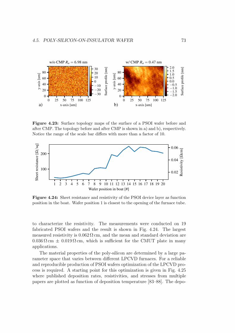
4.5. POLY-SILICON-ON-INSULATOR WAFER 73
0 25 50 75 100 125x-axis [um]
0
20
40
60
80
y-ax
is[u
m]
a)
w/o CMP Ra = 6.98 nm
0 25 50 75 100 125x-axis [um]
0
20
40
60
80
y-ax
is[u
m]
b)
w/ CMP Ra = 0.47 nm
−30−20−100102030
Surf
ace
profi
le[n
m]
−2.0−1.5−1.0−0.50.00.51.01.52.0
Surf
ace
profi
le[n
m]
Figure 4.23: Surface topology maps of the surface of a PSOI wafer before andafter CMP. The topology before and after CMP is shown in a) and b), respectively.Notice the range of the scale bar differs with more than a factor of 10.
1 2 3 4 5 6 7 8 9 10 11 12 13 14 15 16 17 18 19 20Wafer position in boat [#]
100
200
Shee
tres
ista
nce
[Ω/s
q]
0.02
0.04
0.06
Res
istiv
ity[Ω
cm]
Figure 4.24: Sheet resistance and resistivity of the PSOI device layer as functionposition in the boat. Wafer position 1 is closest to the opening of the furnace tube.
to characterize the resistivity. The measurements were conducted on 19fabricated PSOI wafers and the result is shown in Fig. 4.24. The largestmeasured resistivity is 0.062 Ω cm, and the mean and standard deviation are0.036 Ω cm ± 0.019 Ω cm, which is sufficient for the CMUT plate in manyapplications.
The material properties of the poly-silicon are determined by a large pa-rameter space that varies between different LPCVD furnaces. For a reliableand reproducible production of PSOI wafers optimization of the LPCVD pro-cess is required. A starting point for this optimization is given in Fig. 4.25where published deposition rates, resistivities, and stresses from multiplepapers are plotted as function of deposition temperature [83–88]. The depo-

74 CHAPTER 4. CMUT FABRICATION
0
10
20
Dep
ositi
onra
te[n
m/m
in]
a)
[83]This thesis
[84]
10−3
10−1
101
Res
istiv
ity[Ω
cm]
b)
[85][86]
500 525 550 575 600 625 650 675 700Deposition temperature [C]
−600
0
600
Stre
ss[M
Pa]
TensileCompressive
c)
[87][88]
Figure 4.25: The deposition rate, resistivity, and stress as function of depositiontemperature. The circular markers are data from the literature and represents ei-ther boron doped or undoped LPCVD poly-silicon and triangular markers indicatemeasurements of LPCVD boron doped poly-silicon from this thesis.

4.5. POLY-SILICON-ON-INSULATOR WAFER 75
Poly-silicon
Al
Au
Pyrex1 µm
Figure 4.26: Cross sectional SEM im-age of an anodic bonded CMUT fabri-cated using a PSOI wafer.
Poly-silicon
SiO2
Si
Al
1 µm
Figure 4.27: Cross sectional SEM im-age of a fusion bonded CMUT fabri-cated using a PSOI wafer.
sition rates are seen, in Fig. 4.25 a), to increase as function of the depositiontemperature, whereas a reduction in the resistivity is observed in Fig. 3 b)(notice the log y-scale). Hence, rapid fabrication time and low resitivityare gained by increasing deposition temperature. However, the temperaturedependency of the stress is not as unambiguous as the deposition rate andresistivity, and extrapolation is therefore difficult.
The fabricated PSOI wafers have been used for all the fabricated anodicbonded CMUTs and all the CMUTs from the TR1 process described in sec-tion 4.3 and 4.4, respectively. Cross sectional SEM images of both anodicallyand fusion bonded CMUTs can be found in Fig. 4.26 and 4.27, respectively.The CMUTs are tilted 10° in both images to improve the visualization ofthe CMUT structures, and a thin layer of gold is sputtered to prevent di-electric charging of the insulating layer. Both CMUTs are diced using anautomatic dicing saw, and the fact that the poly-silicon plate is intact afterdicing indicates a strong bond. The poly-silicon plates are in both imagesbonded to the post region (right side of the images). Notice, the structure ofsilicon substrate in the TR1 process (right image) is substantially differentfrom the poly-crystalline structure of the plate. Hence, CMUT fabricationusing PSOI wafers are applicable for both fusion bonded and anodic bondeddevices, and PSOI wafers might even provide improved bonding conditionsfor anodic bonded devices. The front and the back side of a SOI wafer willbe electrically insulated from one another. This is a direct consequence ofthe fabrication method of SOI wafers [89] and this is also a desired fea-ture in many applications. However, the insulation is a disadvantage duringan anodic bonding process, since the current has to run though the BOXlayer with poor conducting properties. The anodic bonding temperature, of

76 CHAPTER 4. CMUT FABRICATION
−+
I I
−50 −25 0 25 50Bias [mV]
−300
−150
0
150
300
Cur
rent
[uA
]
R =178Ω
DataFit
Figure 4.28: IV characterization between the front and back of a PSOI wafer,where a resistance of 178 Ω is estimated by a linear fit. The sketch to the leftillustrates how the current flows around the edges of a PSOI due a conformaldeposited of poly-silicon. The results from the IV measurement is shown to theright, where a linear relationship is observed.
approximately 350 C, increases the conductivity of SiO2 multiple orders ofmagnitude [90], and is essential for the success of the anodic bonded pro-cesses. However, the introduction of an additional insulator impedes thebonding current during anodic bonds, which i is inevitable when SOI wafersare involved due to the BOX layer. The BOX layer of an SOI wafer increasesthe electrical resistance during an anodic bonding process, and prohibits theaccumulation of charges in the generated depletion region.
The device layer of a PSOI encapsulates the entire wafer due to a con-formal deposition process, and thereby facilitates a short circuit between thefront and back side. This is confirmed by IV measurements between thefront and the back side of a PSOI wafer, and the result is shown in Fig. 4.28together with an illustrative sketch of how the measurement was conducted.An ohmic relationship is observed in the IV measurement and a resistanceof 178 Ω is estimated by a linear fit. Hence, the front and back side of PSOIwafers are, opposite to SOI wafers, not electrically insulated from each other,and larger bonding bonding currents are therefore expected.
The results of the PSOI wafer is summarized in paper D.
4.6 Chapter summery
Four different row-column fabrication methods were investigated in this chap-ter, and all of the demonstrated methods possessed desirable properties forCMUT based row-column fabrication. The most relevant row-column prop-

4.6. CHAPTER SUMMERY 77
Table 4.3: Row-column CMUT fabrication summery.
LOCOS BCB AnodicLOCOS +
Anodic
Masks 4 3 3 4Breakdownvoltage inpost region
0.74 V/nm 0.08 V/nm 0.92 V/nma 0.74 V/nm
Array yield Low High HighInsufficientstatistics
Requiredsurfaceroughness
< 1 nm High < 50 nm < 1 nm
Substratecouplingfactor
1.6 - 2.5 1.1 1.0b Not known
Fabricationtime
Weeks Days Days Weeks
Highestprocesstemp.
≈ 1000 C ≈ 250 C ≈ 350 C ≈ 1000 C
Clean roomlimitationsc None BCB Pyrex Pyrex
Other - -Short
circuitd -
erties are summarized in Table 4.3, where a green and red color coding havebeen used to emphasize the desired and undesired properties, respectively.Notice, the individual parameters are not equally important.
A low array yield of row-column arrays was observed for the LOCOS basedCMUTs, but excellent CMUT performance was observed for the few success-fully fabricated row-column arrays. Many desirable row-column propertieswere observed for the BCB fabrication process, but the dielectric strength ofthe BCB was simply not suited for CMUTs operated close to the pull-in con-dition. The Anodic bonded and BCB processes share many of desired row-
aDielectric strength found in the literature [91].bSubstrate coupling factor calculated from [46].cContamination rules at the DTU-nanolab clean room facilities.dDescribed in details in section 4.3.

78 CHAPTER 4. CMUT FABRICATION
column properties including structured bottom electrodes, excellent bond-ing properties, low process temperatures among other. But, the dielectricstrength of Pyrex, used in the anodic bonding process, was in the literaturefound to be 0.92 V/nm [91] and therefore more suited for high field appli-cations. A problem with short circuiting between the top and the bottomelectrode was observed for the anodic bonded CMUTs. This problem wasaddressed by introducing an insulating nitride film at the bonding interface.A second generation of anodic bonded CMUTs were designed and fabricatedincluding the additional nitride layer. Preliminary IV measurements sug-gested the new design to be a feasible solution to the problem. The finalpresented CMUT fabrication combined the best properties from the LOCOSprocess and the anodic bonding process. This process was been developedto increase the array yield and reduce the substrate coupling factor relativeto the LOCOS process. Linear arrays of this new process was electricallycharacterized and showed an expected CMUT performance without any in-dications of unwanted charging effects. The row-column performance of thisnew process is still unknown and additional process development is thereforenecessary.
The concept of a PSOI wafer was introduced in the last part of the chapteras an alternative to conventional SOI wafers. The fabrication of multiplePSOI wafers were described and characterized, and the fabrication of twodifferent CMUTs using PSOI wafers were demonstrated.

CHAPTER 5
CMUT characterization
This chapter investigates the acoustical properties of the CMUTs fabricatedduring this thesis. The chapter consists of two parts. The first part consid-ers acoustic characterization of a single linear CMUT element. The analysisincludes characterization of both the acoustic response from the CMUT andthe overall experimental set-up. The transmit impulse response is calcu-lated and bias dependency of the transmit pressure, center frequency, andbandwidth has been measured.The second part of the chapter considers acoustic characterization of thefabricated 92+92 row-column probe. The pressure fields of rows and columnsare measured, and the pressure field is observed to be attenuated long thecolumns. A detailed analysis of electrode resistance is developed and usedto describe the attenuated pressure field for the columns. Volumetric row-column images of wire and cyst phantoms acquired by the developed 92+92RCA CMUT probe are presented in the last part of the chapter.
5.1 Acoustic characterization
A characterization set-up for a single channel system has been developed dur-ing this work. The system is designed to perform an isolated acoustic analysisof CMUT, where the influence from the instruments and the electronics areminimized. This task can be approached either by calibration curves or bychanging the hardware. The frequency response of the overall system dis-torts the applied AC signals, however, the distortion can be accounted for by
79

80 CHAPTER 5. CMUT CHARACTERIZATION
Water
CMUTV0
Hydrophone
Oscilloscope Function generator
THS3120
R2
C1
R1
Power supplyBias-T
Figure 5.1: Sketch of the acoustic set-up. The bias-T consists of a capacitor,C1, and a resistor, R1, with the discrete values of 100 nF and 1 MΩ, respectively.V0 is the nodal point of interest in this analysis and represents the AC signal atCMUT electrode. THS3120 is an operational amplifier used to buffer the outputof the function generator, and the resistor, R2, is required to stabilize the bufferedsignal.
calibration curves. This approach assumes linearity and errors will thereforebe introduced when non-linear CMUTs are investigated. The other approachis to design the electronics such that the frequency response is approximatelyconstant in the frequency range of interest. This approach allows characteri-zation of non-linear systems and will therefore be used in this analysis. Theexperimental set-up is sketched in Fig. 5.1, where the nodal point, V0, willbe the reference point during the analysis. This nodal point represents theactual AC signal at the CMUT electrode, and a completely flat frequencyresponse would be expected for an ideal system without any distortions.
The pressure waves generated by the CMUT are measured by a HGL-0400 hydrophone from Onda. The hydrophone is positioned and aligned4 cm above the transmitting CMUT element, and the measured signal ispicked up by a 5442D oscilloscope from PicoScope using 12 bit resolutionand a sampling frequency of 62.5 MHz. The CMUT has prior to the acousticmeasurements been wire-bonded to a Printed Circuit Board (PCB) and af-terwards covered with PDMS to ensure electrical isolation between elementsduring immersed operation. The signal at the nodal point V0 is also moni-tored by the PicoScope using 10X probes to reduce effects from of capacitiveloading. The applied AC signals are generated by a TexTronix AFG31102arbitrary function generator and the applied DC bias is provided by a Keith-ley 2490 1100V sourcemeter. To reduce the source/generator impedance ofthe measuring system, a wide-band, low noise, high-output drive THS3120operational amplifier is used to buffer the output. The operational amplifier

5.1. ACOUSTIC CHARACTERIZATION 81
is coupled as a non-inverting amplifier with a gain of 5 V/V. The magnitudeof R2 is comparable to commercially available ultrasonic transmitters/driverswhich typically have an output impedance of 7-15 Ω. The resistor, R2, iso-lates the phase shift at high frequency caused by the capacitive load fromthe amplifier feedback path. Resistance values of 5 Ω and 10 Ω have beenused for R2 in this analysis, all other parameters have been kept unchanged.Resistance lower than 5 Ω lead to instabilities in the feedback loop of thebuffer amplifier.
A linear CMUT array from the combined LOCOS and anodic bondingfabrication process is used in this analysis. The side length of the CMUTcell in this array is 70 µm and not 50 µm as specified for the TR1 row-columnarrays, hence, the center frequency and pull-in voltage are lower than thedesigned specifications.Pulses of uniform white noise have been used to characterize the frequencyresponse of both the system and the CMUT. The noise is generated synthet-ically in MatLab and the frequency response is therefore known to be flat forall frequency components (on average). However, the frequency dependencyof the CMUT, the instruments, and electronics cause a distorted frequencyspectrum. Measurements of a noise pulse and the average frequency contentare shown in Fig. 5.2. The length of noise pulse is approximately 15 µs andlong noise pulses are desirable since the information stored in the noise sig-nal scales with the length. The size of the water tank is the limiting factorfor the length of the noise pulse. The water tank has to be large enoughto ensure no reflections from boundaries. The colored part of the excitationsignal showed in Fig. 5.2 a) indicates the part of the signal that is used togenerate the frequency spectrum, notice the first and the last part of thepulse are omitted to reduce transient effects. The average Fourier spectrumof 100 generated noise pulses is shown in Fig. 5.2 b) for two different R2
values. The measured frequency response can be divided into three partsindicated by α, β, and γ. The α part is a constant plateau for frequencieslower than 15 MHz. The β part is a region between 15 MHz and 25 MHzwhere a reduction in the Fourier amplitude is observed. Finally, the γ part isanother constant plateau for high frequencies above 25 MHz. The observedresponse is modelled by an empirical model, Uf , given by
|Uf (f)| = a
2· erfc (b · (f − f0)) + c (5.1)
where a and c are amplitude parameters, f0 defines the frequency at whichthe amplitude difference between a and c has dropped 50%, and b determinesthe width of the β part. The expression f0−1/b is used as a measure for a cut-off frequency, and corresponds to the frequency at which the amplitude has

82 CHAPTER 5. CMUT CHARACTERIZATION
0 10 20 30 40Time [us]
−10
−5
0
5
10E
xcita
tion
sign
al[V
]
a)
0 5 10 15 20 25 30Frequency [MHz]
0.00
0.05
0.10
0.15
0.20
0.25
Four
iera
mpl
itude
[a.u
] α β γ
b)
5 Ω10 ΩFit
Figure 5.2: Analysis of the excitation signal measured at the nodal point, V0.The noise excitation pulse is plotted in a). The data used to generate the Fourierspectrum is colored (red), and the corresponding Fourier spectrum is plotted inb) for two different values of R2. The frequency data is an average of 100 Fourierspectra.
Table 5.1: Fitted parameters for two values of R2
Fitted parameters R2 = 5Ω R2 = 10Ω R2,5Ω/R2,10Ω
a 0.12 a.u 0.11 a.u 9.1 %b 0.20 MHz−1 0.14 MHz−1 42.8 %c 0.049 a.u 0.043 a.u 14.0 %f0 20.3 MHz 19.9 MHz 6.3 %
a+ c 0.17 a.u 0.15 a.u 13.3 %f0 − 1/b 15.3 MHz 12.6 MHz 21.4 %
dropped approximately 16%. The interpretation of c is the amplitude of thelast plateau (part γ), and the sum of a and c is the amplitude of first plateau(part α). An overview of the fitted parameter can be found in Table 5.1. Allthe fitted parameters are observed to increased for R2 = 5Ω when comparedto R2 = 10Ω. An increase of 13.3% is observed for the amplitude of the αplateau (a + c), hence, the AC signal at the CMUT electrode has becomelarger. Additionally, an increase of 21.4% is observed for the cut-off frequencywhich implies a reduced suppression of high frequency components.
The stabilization resistor, R2, perturbs the frequency response of thesystem and thereby also the acoustic performance of the CMUT, which canbe observed in the transmit impulse response. The acoustic response and the

5.1. ACOUSTIC CHARACTERIZATION 83
0.0 0.5 1.0Time [us]
−1
0
1
Nor
mal
ized
impu
lse
resp
onse
a)
5 Ω10 Ω
0.0 0.5 1.0Time [us]
b)
PZT - BK9032
−40
−30
−20
−10
0
Env
elop
e[d
B]
0 2 4 6 8 10 12 14Frequency [MHz]
−40
−20
0
Am
plitu
de[d
B] c)
PZT - BK9032 5 Ω 10 Ω
Figure 5.3: Normalized transmit impulse response of the developed CMUT anda commercial PZT. The results from the CMUT is shown in a) for two values ofR2. The transmit impulse response of a commercial BK9032 probe is shown in b).The solid lines are the impulse responses and is read on the left y-axis, and thedashed lines are the envelopes and is read on the right y-axis. The correspondingtransfer functions are plotted in c). A DC bias of 90 V was used for the CMUTmeasurements corresponding to approximately U/Upi = 85%.
excitation signal have been deconvolved in order to calculate the transmitimpulse response shown in Fig. 5.3 a).
The overall shape of the impulse response is similar in both cases, but,a 26.3% peak-to-peak amplitude increase is observed for R2 = 5Ω. The am-plitude increase corresponds approximately to 2(a+ c), and thus in excellentagreement with the previous analysis. The envelope of the impulse responsesshow the subsequent ring down process is suppressed more than −30 dB for alltimes after the main peak. However, the some of ring down dynamics couldbe numerical noise from the deconvolution operation. The transmit impulseresponse of a BK9032 transducer (5 MHz linear PZT transducer) from BKmedical is shown in Fig. 5.3 b), where a substantial ringing is observed com-pared to the developed CMUT transducer. Notice, the impulse response forthe BK9032 transducer is calculated using a different method described in

84 CHAPTER 5. CMUT CHARACTERIZATION
0 lb f0 ub 10 15Frequency [MHz]
0.2
P0/2
0.6
P0
1.0A
mpl
itude
[a.u
]a)
0 5 10 15Frequency [MHz]
10−2
10−1
100
Am
plitu
de[a
.u]
b)
Figure 5.4: The transfer function of the fabricated CMUT. A single spectrumis plotted in a). The pressure parameter, the center frequency, and bandwidthare indicated are indicated on the axes. Multiple transfer functions where theDC bias has been varied from 10 V to 90 V. The measured data is for R2 =5 Ωconfiguration.
[92]. The corresponding transfer functions are all shown in Fig. 5.3 c), wherea higher bandwidth is observed for the CMUT. All features in the CMUTtransfer function is known to be acoustical effects, since a flat frequency spec-trum has been measured up to 12.6 MHz and 15.3 MHz for R2 = 10Ω andR2 = 5Ω, respectively.
The final analysis in this section investigates how R2 influences the out-put pressure, center frequency, and bandwidth of the CMUT as function ofapplied DC bias. The three parameters are estimated by fitting an empiricalmodel to the transfer function. The model is empirical and given by
P (f) = P0 exp
(− (f − f0)2
2σ20 + fσ2
1
)(5.2)
where P0 is a pressure parameter, σ0 and σ1 are parameters used to calculatethe bandwidth, and f0 is center frequency. The σ1 parameter allows theimpulse response to be asymmetric around the center frequency, which isseen to be the case in for the CMUT transfer function. Notice, the modelbecomes a symmetric Gaussian function in the limit where σ1 → 0, and σ1
is therefore a measure of asymmetry in the transfer function. The modelhas been used to determine parameters for different DC biases. The modelis fitted to a single spectrum in Fig. 5.4 a) and the fitting parameters areindicated on the axes. The same measurement is plotted in Fig. 5.4 b) fornine different DC biases ranging from 10 V to 90 V.

5.1. ACOUSTIC CHARACTERIZATION 85
The fitted parameters are plotted plotted in Fig. 5.5 as function of ap-plied DC bias. The pressure parameter, P0, is observed to monotonicallyincrease with the applied bias and the 5 Ω configuration emits more pressureas expected. The center frequency is observed to decrease with the appliedbias. Both observations are in perfect agreement with the CMUT theoryfrom chapter 2. The decrease of the bandwidth is not fully understood, andthis phenomenon has not to the author best knowledge, not been describedin the CMUT literature. The observation could be explained by an increasedimaginary part of the radiation impedance. The decrease in the center fre-quency lowers the ka value and therefore introduces a higher mass loadingof the water in front of the CMUT, the additional mass increases the charac-teristic decay time and thereby reduces the bandwidth. However, the effectof the bandwidth is small relative to the effect on the center frequency, itis seen from the the Fractional BandWidth (FBW). The fraction bandwidthincreases from 117% to approximately 130% between the smallest and largestapplied voltage. Finally, the output pressure is clearly perturbed by the theR2 stabilization resistor, but, the center frequency and the bandwidth aresimilar for both values of R2.

86 CHAPTER 5. CMUT CHARACTERIZATION
0.0
0.5
1.0
P 0
a) 5 Ω 10 Ω
3.8
4.0
4.2
4.4
f 0[M
Hz]
b)
4.9
5.0
5.1
5.2
FWH
M[M
Hz]
c)
10 20 30 40 50 60 70 80 90DC bias [V]
115
120
125
130
FBW
[%] d)
Figure 5.5: The fitted parameters as function of applied DC bias for two valuesof R2. a) Normalized pressure. b) Center frequency. c) Bandwidth (FWHM). d)Fractional bandwidth.

5.2. ELECTRODE RESISTANCE 87
5.2 Electrode resistance
The 92+92 LOCOS RCA CMUT array is characterized in this section, andthe electrode resistance is an essential part of this analysis. A change interminology will be introduced to uniquely define the electrodes. The topand bottom electrodes will be used instead of rows and columns, respectively.The reason being that rows and columns are not uniquely defined, since rowsbecome columns after a 90° rotation of a RCA array. Using the top andbottom terminology allows a unique description that is invariant to rotation.
A characterization of the transmit pressure showed a significant pressure pres-sure difference between the rows and columns. The peak-to-peak amplitudeof the impulse responses differs a factor of 3.5 between rows and columns asseen in Fig. 5.6 a). The difference is caused by high resistance in the bottomelectrode, which will be shown in this section. The frequency components ofthe impulse response are shown in Fig. 5.6 b), where a magnitude differencebetween top and bottom electrodes is observed to be frequency dependent.The difference between the bottom and top is plotted in Fig. 5.6 c). An ex-ponential tendency is observed (semilog plot) between 2.5 MHz and 15 MHz,and the attenuation is estimated to −1.0 dB/MHz in this region.
The top electrode is made by aluminum and the bottom electrode is madeby doped silicon. The electrical resistivity differs substantially between thetwo materials. The resistivity of metal electrodes is on the order of 10−6 Ωcm[93], while the resistivity of a silicon electrode varies from 104 to 10−4 Ωcmdepending on the doping level [94]. The resistance in the electrode has to besufficiently low to achieve acceptable performance of the CMUTs, which inmost cases never become an issue for metal electrodes due to their low re-sistivity. However, in special cases it becomes challenging to use even highlydoped silicon, particularly for long elements such as row-column elements.If the resistivity in an electrode is too high, the overall system will behaveas a low-pass filter, which will attenuate applied AC signals along the elec-trodes. A non-uniform transmitting element will skew the transmitted fieldand seriously degrade the receive focusing.
A delay line model is used to mathematically describe the attenuationof the AC signal along a CMUT element. The element is lumped into adistributed network of resistors and capacitors as shown in Fig. 5.7, wherea) shows a common CMUT design with an equivalent circuit on top. Theresistivity of the electrode determines the magnitude of the resistors. Thevariable capacitors represent CMUT cells and the constant capacitors rep-resent the parasitic capacitance. The electronic circuit can be described byResistor Capacitor delay line model if the electrical components are lumpedtogether as shown in Fig. 5.7 b). In this model the resistors and capac-

88 CHAPTER 5. CMUT CHARACTERIZATION
0.0 0.1 0.2 0.3 0.4 0.5Time [us]
−1.0
−0.5
0.0
0.5
1.0
Impu
lse
resp
onse
[a.u
]
a) Top Bottom
0.0 2.5 5.0 7.5 10.0 12.5 15.0 17.5 20.0Frequency [MHz]
−40
−20
0
Am
plitu
de[d
B]
b)
0.0 2.5 5.0 7.5 10.0 12.5 15.0 17.5 20.0Frequency [MHz]
−20
−10
0
Am
plitu
de[d
B]
c)
slope = -1.0 dB/MHz
Bottom − TopFit
Figure 5.6: Impulse response for rows and columns in both time and frequencydomain. a) The average transmit impulse response for both top and bottom elec-trodes. The impulse response magnitude of the bottom electrode is approximatelyreduced by a factor of 3 compared with top. b) The corresponding transmit transferfunction for the top and bottom electrodes. The shape of the transfer functions aresimilar despite the reduced amplitude for the bottom electrodes. c) The transferfunction for the top electrodes subtracted from the transfer function of the bottomelectrodes. In the region between 2.5 MHz and 15 MHz an exponential tendency(dB scale) is observed, and attenuation is estimated by fitting a linear function tothe dB compressed data. The calculated impulse responses are averaged from 50measurements.

5.2. ELECTRODE RESISTANCE 89
Luin uout
a)
Rd
Cd
∆x.) b)
uin uout
Figure 5.7: Model of the Row-Column addressed CMUT array. a) Idealizedmodel of a Row-Column element. The resistance through the element is modelledby resistors, the CMUTs cells are modelled as variable capacitors, and the par-asitic capacitance is modelled as constant capacitors. b) When the capacitanceof the CMUTs and the parasitic capacitance are merged together, the circuit isdescribed as a Resistor Capacitor (RC) delay line. Rd and Cd are the resistanceand capacitance of a distributed segment of length ∆x and are related to the totalresistance and capacitance by Rd = R/L ·∆x and Cd = C/L ·∆x.
itors are assumed to be evenly distributed along the element, Rd and Cd,are resistance and capacitance of a distributed segment of length ∆x. Thesequantities are related to the total resistance, R, and the total capacitance C,by
Rd =R
L∆x Cd =
C
L∆x, (5.3)
where L is the length of the element. The capacitance and resistance of aCMUT element can be mathematically formulated as
C =εWL
g, (5.4)
and the resistance of an element with an uniform cross-sectional area is [94]
R =%L
HW, (5.5)
where ε is the relative permittivity, W is the width of the element, and g isthe gap height, H is the electrode thickness. The resistivity % of silicon canvary eight orders of magnitude depending on the doping level, and is thereforea crucial parameter in the electrical design process of a CMUT. Under theassumption of constant capacitance and resistance and in the limit where∆x → 0, the voltage distribution u(x, t) in a delay line is governed by thediffusion equation
∂u (x, t)
∂t=
L2
RC
∂2u (x, t)
∂x2. (5.6)

90 CHAPTER 5. CMUT CHARACTERIZATION
During operation will a CMUT element be subject to the following boundaryconditions and initial condition
u(0, t) = U0g(ωt) (5.7)
∂u(x, t)
∂x
∣∣∣∣x=L
= 0 (5.8)
u(x, 0) = 0, (5.9)
where U0 is the amplitude of the excitation, and ω and g(ωt) are the angularexcitation frequency and excitation function, respectively. The first boundarycondition (5.7) corresponds to the input signal at the electrode pad. Thesecond boundary condition (5.8) states that the current density is zero at theend of the electrode, hence, the flux is zero. The initial condition (5.9) implieszero AC voltage at t = 0. The system contains some intrinsic characteristicparameters and by introducing x = x/L, t = ωt, and u = u/U0 allow Eqn. 5.6to be rewritten on a dimensionless form
∂u
∂t= D
∂2u
∂x2where D =
1
ωRC. (5.10)
The product ωRC is here seen to be the determining parameter of this sys-tem, and can be interpreted as an inverse diffusion coefficient. The ωRCproduct can be expressed in terms of geometry and material properties byusing Eqn. 5.4 and Eqn. 5.5, that provides the following scaling properties
ωRC = ωεWL
g
%L
HW= ω
ε%L2
gH∝ L2
H. (5.11)
The length of an electrode has a square dependence on the ωRC product,and the height of the electrode has an inverse dependence, whereas the widthof the element cancels out. Hence, the parameter space suitable for a shortCMUT elements are much larger than the parameter space of long element.Typical sizes of the different types of CMUT elements are sketched in Fig. 5.8.
A more quantitative analysis requires a solution to Eqn. 5.10, whichwill be given in both the frequency and time domain. The frequency domainanalysis provides a significant reduced complexity, that enables a closed formsolution that is used to define a criterion for the upper bound of ωRC. Eigen-function expansion is used for the analysis in time domain analysis, and aninfinite series representations is used to evaluate transient response of thesystem.

5.2. ELECTRODE RESISTANCE 91
L
L/5
L/20
Row-Column
Linear
Test structure
Figure 5.8: The size difference between a common RCA element, a linear elementand a test structure.
The diffusion equation does not have a closed-form solution when theparticular initial and boundary conditions (Eqn. 5.7 to Eqn. 5.9) are imposed.However, a closed form solution of the transfer function can be found in thefrequency domain. After a Fourier transform, F , Eqn. 5.6 can be expressedas
∂2U
∂x2− κ2
L2U = 0 (5.12)
whereF u = U and κ2 = iωRC. (5.13)
By imposing the transformed boundary conditions
F u(0, t) = V0G(ω) (5.14)
F∂u(x, t)
∂x
∣∣∣∣x=L
= 0 (5.15)
the final solution becomes
U(x, ω) = V0G(ω)cosh
(κ(
1− x
L
))
cosh(κ)︸ ︷︷ ︸H(x,ω)
, (5.16)
where H(x, ω) is the transfer function of the system. The product ωRC ap-pears again in the frequency domain analysis, and its impact on the transferfunction is plotted for different values in Fig. 5.9 a) and b), for both theabsolute magnitude and phase, respectively.
The absolute magnitude decays along the element, and it translates intoa decreasing AC magnitude along the element. Hence, the emitted pressurewill be highest near the contact pad and then attenuate along the element.The attenuating effect becomes more pronounced as ωRC increases. The

92 CHAPTER 5. CMUT CHARACTERIZATION
0.0
0.5
1.0
|H(x,ω
)|
a)
ωRC = 0.35ωRC = 2
ωRC = 4ωRC = 10
ωRC = 20ωRC = 30
0.0 0.2 0.4 0.6 0.8 1.0x/L
0
−π2
−π
− 3π2
6(H
(x,ω
))
b)
Figure 5.9: The transfer function as function of normalized distance for sixdifferent values of ωRC. a) The magnitude of the transfer function, in the DC casewhere ωRC → 0 the potential becomes uniformly distributed along the element.As ωRC increases, the AC potential drop along the element, becomes larger. b)The phase of the transfer function. For ωRC 1 the pressure will approximatelybe emitted simultaneously along the element, however, for larger values of ωRC asignificant delay is predicted along the element.
phase shift along the element is also influenced by ωRC, so a transmittedpulse will be time delayed along the element. Equivalently to the magnitude,the higher ωRC value the more pronounced effect. Consequently, at the endof an element, the applied AC signal becomes increasingly time delayed andattenuated as ωRC increases. The design criterion is found by evaluating theabsolute magnitude of the transfer function at the end of an element, whereH(x, ω) simplifies to
H(L, ω) =1
cosh(κ). (5.17)
A criterion of a 1% potential drop is used as a guideline to get close to auniform acoustic pressure along the element. In terms of phase shift alongthe element, this criterion corresponds to a delay of −0.17 rad or −9.7°. The

5.2. ELECTRODE RESISTANCE 93
0.00
0.25
0.50
0.75
1.00
|H(L,ω
)|
a)
|H(L,ω)|> 0.99|H(L,ω)|< 0.99
10−2 10−1 100 101 102 103
ωRC
0−2π−4π−6π−8π
6(H
(L,ω
))
b)
Figure 5.10: The transfer function at the end of the element (x = L) as functionof the product ωRC. a) The absolute magnitude at the end of an element, whereat 0.99 is indicated with a dashed line. The green region indicates that the mag-nitude of the transfer function is above above 0.99 and the red region indicates amagnitude less than 0.99. b) The phase delay at the end of an element. The 0.99magnitude threshold is also indicated on this plot, and the criterion correspondsto a delay at the end of -0.17 radians or -9.7 degrees.
magnitude and phase of the transfer function at the end of the element areplotted as a function of ωRC in Fig. 5.10 a) and b), respectively.
The green area indicates the regime where this criterion is satisfied andred where it is not. A numerical solution of Eqn. 5.17 shows that the criterionis met when
ωRC < 0.35. (5.18)
This criterion limits the acceptable parameter space for RCA arrays. Thespecified imaging properties such as center frequency and channel count de-termine the size of a row-column array. Consequently, the electrode thicknessand resistivity are the only design variables, are two options are possible,either a low resistivity or a thick electrode, which can be concluded fromFig. 5.11 where the expression for ωRC is in a contour plot.
Highly doped silicon is necessary to satisfy the 0.35 criterion and prefer-ably combined with a thick electrode. A thick electrode is desired from anelectrical point of view, but, thick electrodes require additional dry etchingin the fabrication process. Long dry etch processes are not necessarily prob-lematic, however, the probability of particle redeposition increases with the

94 CHAPTER 5. CMUT CHARACTERIZATION
2.0 9.0 16.0 23.0 30.0Electrode thickness [um]
10−4
10−3
10−2
Res
istiv
ity[Ω
cm]
ωRC
0.100
0.350
1.0002.000
4.00010.000
10−1
100
101
Figure 5.11: ωRC parameter space. Assumed values for calculation of ωRC:L = 2 cm,W = 90 µm, C0 = 100 pF, and fmax = 10 MHz.
etching time, that later can lower the bonding yield. SOI wafers that satisfythe ωRC criterion are highly specialized wafers and not a common productin the SOI wafer industry. This statement is illustrated on the scatter plotin Fig. 5.12. The scatters represents the SOI wafer stock list from Ultrasil.The size of the scatter indicates the quantity of the given wafer batch, anda transparent color scheme has been used to enable visualization of multiplebatches with similar properties. The dashed lines outline different valuesof ωRC, and the green region indicates the parameter space that satisfiesthe developed criterion. The majority of the stock list wafers are observedviolate the criterion, and only few wafer batches satisfy the criterion. Addi-tional SOI parameters have been omitted in this analysis. These parametersinclude thickness of the BOX and handle layers, wafer bow, doping type, andcrystal orientation are also influential on the CMUT fabrication.
The developed ωRC criterion is difficult to verify directly, especially forthe bottom electrodes. The attenuation along the bottom electrode cannot beprobed using common electrical characterization, since the bottom electrodesare beneath the surface of the array. An indirectly verification of this effectcan be done by measuring the transmit pressure along the element.
By using the RCA scheme, it is possible to actuate the same CMUTscells, either using the rows or the columns. Thus, effects that do not origi-nate from the electrode configuration should be present is both cases. Thetransmit pressure field is measured for all elements individually at a distance

5.2. ELECTRODE RESISTANCE 95
101 102
Device layer thickness [um]
10−5
10−3
10−1
101
103
Res
istiv
ity[Ω
cm]
ωRC = 0.35 ωRC = 1 ωRC = 20 Ultrasil SOI stock
Figure 5.12: Available 4” SOI wafer stock list from Ultrasil mapped in the re-sistivity versus device layer thickness parameter space. The size of the scattersindicates quantity of the available SOI wafer batch. and scatter are made trans-parent to enable visualization of multiple batches with the same resistivity anddevice layer thickness. The green area indicates the region that satisfies the ωRCcriterion. The used wafer stock list is from the 23th of august 2019. Assumed valuesfor calculation of ωRC: L = 2 cm,W = 90 µm, C0 = 100 pF, and fmax = 10 MHz.

96 CHAPTER 5. CMUT CHARACTERIZATION
-11 -5.5 0 5.5 11x [mm]
11
5.5
0
-5.5
-11
y[m
m]
a)
Top odd
-11 -5.5 0 5.5 11x [mm]
11
5.5
0
-5.5
-11
y[m
m]
b)
Top even
-11 -5.5 0 5.5 11x [mm]
11
5.5
0
-5.5
-11
y[m
m]
c)
Bottom odd
-11 -5.5 0 5.5 11x [mm]
11
5.5
0
-5.5
-11
y[m
m]
d)
Bottom even
0
−5
−10
−15
−20
Am
plitu
de[d
B]
Figure 5.13: Average peak-to-peak pressure field for the 92+92 RCA transducer.The numbering scheme of the elements is important, even and odd elements areaveraged separately. The pressure fields from the top electrodes are shown in a) andb), and the pressure fields from the bottom electrode are shown in c) and d). Thetop electrodes are unaffected by the numbering scheme, whereas an anti-symmetryis observed for the bottom electrodes between the odd and even elements. Themaximum pressure is measured near the edge closest to the electrical connectionand the pressure decreases along the element.
of 1 cm using an AIMS III intensity measurement system (Onda Corpora-tion, Sunnyvale, CA, USA) with an Onda HGL-0400 Hydrophone connectedto the experimental research ultrasound scanner, SARUS [95]. The elementsare excited by a six-cycle sinusoidal pulse at different frequencies. Six cy-cles were chosen to ensure the correct excitation frequency by minimizingtransient effects. The pressure field is mapped by moving the hydrophonein the x-y plane in front of the transducer, and resolved in a 45 × 45 gridwith a spacing of 0.5 mm. The pressure fields of all elements (both top andbottom) have been measured by probing all frequencies in each grid point.The averaged peak-to-peak pressure fields for the top and bottom electrodesare shown in Fig. 5.13. The probe is excited at the center frequency of4.5 MHz and each plot has been normalized to its own maximum and dBcompressed. The odd and even refer to numbering scheme of the elements,

5.2. ELECTRODE RESISTANCE 97
and it becomes important since the all even elements are wire bonded onone side of the array and the odd elements are wire bonded to the oppositeside. The top electrodes are unaffected by the numbering scheme, whereas asignificant change is observed for bottom electrodes. The bottom electrodesemit pressure unevenly along the element, and the pressure output is atten-uated along the element. Most pressure is emitted at near the contact andleast pressure is emitted in the opposite end. The top electrodes shown inFig. 5.13 a) and b) have an ωRC value of 0.03 and thereby satisfying thedeveloped criterion of Eqn. 5.18, and the pressure distribution is observed tobe uniformly distributed along the element. The bottom electrodes shownin Fig. 5.13 c) and d) have an ωRC value of 21.4 and violate the criterion.Hence, the measured attenuation in the pressure field is expected accord-ing to the developed theory. The pressure drop along an element should bequalitatively comparable with the theory from the delay line model, and thetransfer function is compared to measurements in Fig. 5.14.
The delay line model is plotted in Fig. 5.14 a) for comparable valuesof ωRC. The mean and standard deviation of the peak-to-peak pressurefields along the center of an element are plotted in Fig. 5.14 b) and c) forthe 92+92 and 62+62 RCA CMUT probes, respectively. The solid linesrepresent the bottom electrodes and the dashed lines the top electrodes.Only one pressure profile has been plotted for the top electrodes due to thesame behaviour for the other excitation frequencies. The highest frequency of7 MHz is used as a representation for the worst case scenario in terms of ωRC.Each pressure profile has been normalized to its own maximum to obtain afair comparison between the different frequencies. Higher values of ωRC isobserved to increase the attenuation along the electrode in good agreementwith the transfer function model. The expected pressure drop at the endof an element are according to the model 76%, 92%, and 96% for 2 MHz,4.5 MHz, and 7 MHz, respectively. However, the measured pressure drop isobserved to be 63%, 74%, and 82% for the same excitation frequencies, andthe model does therefore overestimate the measured values. The discrepancybetween Fig. 5.14 a) and b) could partly be due to an excitation voltage Uacof 75 V, corresponding to 41% of the 180 V applied DC bias, in which caseU2ac becomes non-negligible. Nonlinear effects could be reduced by lowering
the applied AC voltage, however, these parameters are chosen to imitate realoperation conditions for medical imaging. Another reason for the discrepancyis the estimation of ωRC, where in particular the resistance is uncertain. TheSOI wafer used for the bottom electrodes is specified with an upper bound onthe resistivity of 0.1 Ω cm, and this was used for estimating ωRC. The trueωRC value could, therefore, be lower, and thereby decrease the discrepancybetween theory and experiment. Yet another reason could be transient effects

98 CHAPTER 5. CMUT CHARACTERIZATION
0.00
0.25
0.50
0.75
1.00
1.25
|H(x,ω
)|
a)
2 MHz (ωRC = 9.5)4.5 MHz (ωRC = 21.4)
7 MHz (ωRC = 33.3)7 MHz (ωRC = 0.03)
0.00
0.25
0.50
0.75
1.00
1.25
Nor
mal
ized
pres
sure
b)
0.0 0.2 0.4 0.6 0.8 1.0Normalized distance x/L
0.00
0.25
0.50
0.75
1.00
1.25
Nor
mal
ized
pres
sure
c)
3 MHz (ωRC = 0.4)3 MHz (ωRC = 0.02)
Figure 5.14: Comparison between measurements and theory. a) Transfer func-tion of the delay line model. b) Measured average peak-to-peak pressure dropsalong elements for the probe 92+92 RCA probe. c) Measured average peak-to-peak pressure drops along elements for the 62+62 RCA probe from [31]. Solidlines: bottom electrode. Dashed lines: top electrode. Shaded area: one stan-dard deviation. The same qualitative tendency is observed in a) and b), whichdemonstrates the consistency between measurement and theory.

5.2. ELECTRODE RESISTANCE 99
which are not accounted for in the frequency domain analysis. These effectcan, however, be included if Eqn. 5.10 is solved in the time domain. Ananalysis performed by EigenFunction Expansion (EFE) can be used to findan infinite series solution. A harmonic excitation is needed if the time andfrequency analysis are to be compared. A continuous sinusoidal excitation isused instead of the general excitation function g(ωt) which therefore altersthe initial condition to
u(0, t)
= sin(t). (5.19)
Apart from the nondimensionalization the two boundary conditions are un-changed. Under these conditions the solution to the diffusion equation isfound to be
u(x, t) = sin(t) +∞∑
n=1
An
1 +(λnωRC
)2
[sin(t) +
λnωRC
[cos(t)− exp
(− λnt
ωRC
)]]
× sin
((2n− 1)πx
2
).
(5.20)
Where an amplitude parameter, An, and the eigenvalues of the system, λn,are defined as
An =4
π(1− 2n)and λn =
(2n− 1)2π2
4. (5.21)
Valuable information can still be extracted despite the complexity of the in-finite series solution provided by EFE. The first sin(t) term is completelyindependent of the position, and will therefore provide a uniform voltagedistribution along the element. Voltage variations along the elements aretherefore solely determined by the sum, and the magnitude of the sum de-pends strongly on the ωRC product. The contribution from the infinite sumvanishes for small values of ωRC in excellent agreement with the frequencydomain analysis. The transient dynamics is observed to be determined byan exponential decay with a rate parameter or characteristic time scale thatalso depends on ωRC. All these effects can be summarized by investigatingthe first cycle of the sinusoidal excitation which is plotted in Fig. 5.15 a) toh) for ωRC = 20.
The colored line the EFE solution and the black dashed line is the fre-quency domain model. An overshoot is observed during the first cycle of theEFE solution relative to the frequency model. The peak-to-peak pressureare therefore expected to be higher according the EFE analysis, which could

100 CHAPTER 5. CMUT CHARACTERIZATION
−1
0
1
u(x,
t)
a)
t = 0.06T0
b)
t = 0.20T0
EFE ±|H(x,ω)|
c)
t = 0.33T0
−1
0
1
u(x,
t)
d)
t = 0.46T0
e)
t = 0.60T0
f)
t = 0.73T0
0.0 0.5 1.0x/L
−1
0
1
u(x,
t)
g)
t = 0.87T0
0.0 0.5 1.0x/L
h)
t = 1.00T0
0.0 0.5 1.0x/L
i)
t = 5T0 to t = 6T0
Figure 5.15: Time domain solutions the Eqn. 5.10 for ωRC = 20. The solid linesare the EFE solution and the black dashed lines are the frequency domain transferfunction (Eqn. 5.16). Snapshots of the first sinusoidal cycle are plotted between a)and h), and the time stamp of the snapshot is shown above each plot and definedin terms of the period T0. Multiple snapshots are shown in i) for 15 differenttimes between 5T0 and 6T0. The transient effects are highly suppressed and thefrequency transfer function confines the upper and lower bound as expected.

5.3. ULTRASOUND IMAGING RESULTS 101
explain the discrepancy between measurements and theory in Fig. 5.14. Themaximum amplitude of the time and frequency model must equal in thelimit where t→∞ or when the transient contributions vanishes as shown inFig. 5.15 i), where the EFE solution is observed to be confined within thebounds of the frequency transfer model as expected.
5.3 Ultrasound imaging results
Two of the 92+92 RCA arrays from section 4.1 have been assembled intoprobes, one with and one without an integrated compound diverging lens.Both arrays suffers from too large electrode resistance in the bottom elec-trodes, and the imaging capabilities are therefore limited. The compoundlens introduces an additional frequency dependent loss mechanism that re-duces the output pressure and SNR even further and images were thereforenot generated by this probe, but characterization of the lens properties andtransmit impulse response of this probe can be found in paper E.
A set of volumetric images were acquired by the 92+92 RCA probe with-out lens. The RF data was acquired by the SARUS experimental scanner[95]. The CMUT probe was biased with 190 V corresponding to 83% of thepull-in voltage, and excited with an ±75 V AC pulse. The pulse for theimaging sequence was four cycled 4.5 MHz sinusoidal pulse.
The three spatially orthogonal images planes of a multi wire phantom hasbeen imaged by the developed RCA probe and shown in Fig. 5.16. The wiresare resolved at a depth of 14 cm and detected in all three planes. Distin-guishable wires are observed for all depths in the elevation plane, however,the first five layers of wires are not detected in azimuth plane due to a mis-alignment between transducer and phantom. The C-plane image is acquiredat a depth of 40 mm and confirms the missing wires in the azimuth planeare caused by misalignment. Row-column images of cyst phantoms have alsobeen acquired and showed in Fig. 5.17. Cysts are detected in all three planes,but due to a significant misalignment between transducer and phantom aresome of the cysts only partially in the field of view . Three cysts are observedin the azimuth plane, all indicated with dashed yellow circles. The third cystis just barely in the field of view, but the circumference is observable, whichthereby demonstrates 3D imaging capabilities down to a depth of 70 mm.The C-plane image is acquired at a depth of 50 mm, and yellow dash linesare imposed on top of the image to indicate the shape of the cyst.

102 CHAPTER 5. CMUT CHARACTERIZATION
-19 0 19Elevation [mm]
10
30
50
70
90
110
130
150
170
Ran
ge[m
m]
-19 0 19Azimuth [mm]
10
30
50
70
90
110
130
150
170
Ran
ge[m
m]
-19 0 19Azimuth [mm]
-19
0
19
Ele
vatio
n[m
m]
C-plane
0−20−40[dB]
Figure 5.16: Volumetric imaging of a wire phantom. The images were acquiredby the developed 92+92 RCA CMUT probe w/o lens. Three orthogonal planes(azimuth, elevation, and the C-plane) are shown from a volume of 3.8 cm × 3.8 cm× 17 cm using a dynamic range of 40 dB. The C-plane is acquired at depth of40 mm.
5.4 Chapter summery
An acoustic white noise analysis was presented. The white noise analysiswas used to characterize the frequency response of the overall CMUT systemincluding electronics and instruments. A flat frequency spectrum between0 MHz up to 15.3 MHz was demonstrated for a developed single channelacoustic experimental set-up. The transmit impulse response of the char-acterized CMUT was calculated using the white noise data. The ring-downamplitude was observed less than −30 dB for all times after the main peak.Additionally, the parameters transmit pressure, center frequency, and band-width were estimated as function of the applied bias. The result showedan expected pressure increase, a reduced center frequency, and a fractionalbandwidth increase from 115% of 130%. A criterion of how to design to de-sign row-column electrodes were derived and demonstrated experimentally.

5.4. CHAPTER SUMMERY 103
-19 0 19Elevation [mm]
0
10
20
30
40
50
60
70
80
90
100
110
120
130
Ran
ge[m
m]
-19 0 19Azimuth [mm]
0
10
20
30
40
50
60
70
80
90
100
110
120
130
Ran
ge[m
m]
-19 0 19Azimuth [mm]
-19
0
19
Ele
vatio
n[m
m]
C-plane
0−20−40[dB]
Figure 5.17: Volumetric imaging of a cyst phantom. The ultrasound images wereacquired by the developed 92+92 RCA CMUT probe w/o lens. Three orthogonalplanes (azimuth, elevation, and the C-plane) are shown from a volume of 3.8 cm× 3.8 cm × 17 cm using a dynamic range of 40 dB. Three cysts are detectable inthe azimuth plane which is indicated with transparent dashed yellow circles. TheC-plane is acquired at depth of 45 mm.
The developed criterion was used to characterize the acoustic performanceof a developed 92+92 row-column probe. The criterion can be used to en-sure less than 1% attenuation of AC signals along a row-column element,which mathematically is formulated as ωRC < 0.35. Finally, volumetricultrasound images acquired by one of the developed 92+92 row-column ad-dressed CMUT probe were presented. 3D images of a wire phantom showeda clear separation between wires in all three dimensions, and the wires weredistinctly resolved down to a depth of 14 cm. In addition, images of a cystphantom demonstrated visualization of cysts down to depth of 7 cm in allthree dimensions.

104 CHAPTER 5. CMUT CHARACTERIZATION

CHAPTER 6
Conclusion
This thesis has presented the results of the PhD project entitled Microma-chined Integrated 2D Transducers for Ultrasound Imaging. The main goalof the project was to develop ultrasound transducer technology for three di-mensional ultrasound imaging, and more specifically development of largerow-column arrays. This goal has been attained.The scaling laws for row-column addressed arrays are highly favourable asthe channel count increases linearly with the number of elements, whereasconventional fully populated matrix arrays have a quadratic dependency. ACapacitive Micromachined Ultrasonic Transducer (CMUT) technology plat-form was chosen as the transducers technology in this work due to the designflexibility and the desirable imaging properties offered by this technology.
In chapter 2, a theoretical analysis of the a single CMUT cell was given.All derived equations were non dimensionalized to provide valuable informa-tion regarding the scaling law of relevant CMUT characteristics. The scalinglaw of the pull-in voltage was derived for a non-linear spring model and fora non-linear clamped plate applied to an electrostatic pressure. A perturba-tive solution to the deflection of the clamped plate problem and the scalingproperties of pull-in voltages were determined. The dynamics of a singleCMUT cell was analyzed using a non-linear harmonic oscillator model in thelow and high ka regimes. The low ka analysis demonstrated a reduction ofthe resonance frequency due to an additional mass loading. This frequencyreduction was observed to depend on the aspect ratio of the CMUT plateand the density ratio between the medium and the plate material. A phaseportrait analysis was used for the high ka regime to rapidly visualize the dy-
105

106 CHAPTER 6. CONCLUSION
namics of various initial conditions. The parameter space was from the phaseportrait analysis observed to depend on the applied bias and the damping ofthe CMUT plate.
Various concepts of the row-column addressing scheme were described inChapter 3. A brief literature review was first given followed by the scalinglaws of the transducer area and imaging resolution capabilities (FWHM) forboth row-column arrays and conventional fully populated matrix arrays. Anexplanation of an undesired row-column specific edge wave phenomenon wasgiven, and an integrated apodization scheme was implemented into all CMUTdesigns in this work to reduce the effect from edge waves. The last part ofthe chapter described a capacitive substrate coupling, which lead to increasedparasitic capacitance for the columns. A 62+62 CMUT row-column probefrom the literature was used as a reference for this work. The capacitanceof the columns was observed to by a factor of 2.5 higher than the rows forthis probe. The capacitance difference was caused by capacitive substratecoupling, and the substrate coupling factor of 2.5 was used as a benchmarkthroughout the thesis.
In chapter 4 four different microfabrication processes of row-column ad-dressed CMUT arrays were described. Two 92+92 row-column transducerswith integrated apodization were fabricated and assembled into ultrasoundprobes, one with a divergent lens and one without. The used fabricationmethod relied on Local oxidation of silicon (LOCOS) and the process wasobserved to unsuitable for fabrication of row-column arrays due to a lowarray yield. The substrate coupling factor of these arrays were reduced to1.6, and impedance measurements showed a coupling coefficient of 15.8%for the LOCOS arrays. The diverging properties of the row-column probewith lens are discussed in paper E. A polymer based CMUT fabrication us-ing polymerBenzoCycloButene (BCB) as spacer and post material was alsodeveloped. An electrically insulating glass substrate was used for the BCBCMUT to reduce to substrate coupling, the reduction was demonstrated a62+62 row-column CMUT array with integrated apodization. The capaci-tance measurements of the rows and columns showed a substrate couplingfactor of 1.1, hence a significant reduction compared to the LOCOS process.Stability tests and acoustic characterization of linear BCB CMUT arrays arereported in paper A. However, the dielectric properties of the BCB polymerwas characterized and showed a median breakdown voltage of 0.08 V/nm.The BCB fabrication process was therefore not suitable for medical imagingapplications where breakdown fields strengths of 0.5 V/nm or even higherare required. The third demonstrated row-column fabrication process wasbased on principle of the anodic bonding. Multiple row-column arrays werefabricated and the developed process showed to be well suited fabrication of

107
large area structures such as row-column addressed arrays. Electrical charac-terization showed an issue with short circuiting between the top and bottomelectrodes. This issue was addressed by introducing a nitride film at thebonding interface, and preliminary measurements implied the new approachsolved the problem. The acoustic performance of the anodic bonded CMUTsare yet to be determined, and measurement strategies are currently beingplanned. The best properties from the LOCOS process and the anodic bond-ing process were combined in the fourth and final fabrication process wherethe intended application was a large 188+188 row-column addressed CMUTprobe. A novel zig-zag element configuration was developed for this probeto fulfill a λ/2 pitch constraint while preserving a closely packed CMUT celllayout. A simulation study of the zig-zag element configuration can be foundin paper B. The fabrication of the 188+188 row-column arrays are still beingdeveloped. The fabrication of the row-column arrays were not fully success-ful due to rupture of the CMUT plate. However, impedance measurementson linear arrays was demonstrated where an expected CMUT behaviour wasobserved and the electromechanical coupling coefficient was estimated to be7.8%.The last part of the chapter described a novel fabrication method of a Poly-Silicon-On-Insulator (PSOI) wafer suited for CMUT applications. Purchas-ing conventional 4” SOI wafers, for CMUT fabrication at a university level,has gotten increasingly more difficult during the last coupled of years. Thedeveloped PSOI technology is intended as a substitution for conventionalSOI wafers, and multiple PSOI wafers were demonstrated in this work. ThePSOI wafers were shown to be applicable to both fusion bonded and an-odically bonded CMUTs. The surface roughness of the PSOI device layerwas measured to 0.47 nm, and the device layer resistivity was measured to0.036 Ω cm ± 0.019 Ω cm. Additional results and findings are presented inpaper D.
In chapter 5, an acoustic white noise analysis was presented. The whitenoise analysis was used to characterize the frequency response of the over-all CMUT system including electronics and instruments. A flat frequencyspectrum between 0 MHz up to 15.3 MHz was demonstrated for a developedsingle channel acoustic experimental set-up. The white noise analysis was ad-ditionally used to acoustically characterize a linear CMUT array fabricatedby the combined LOCOS and anodic bonding method. The transmit impulseresponse was calculated, and the amplitude of the ringing was observed lessthan −30 dB. Additionally, an analysis of relevant CMUT parameters wasprovided as function of the applied bias. The result showed an expectedpressure increase, a reduced center frequency, and a fractional bandwidthincrease from 115% of 130%.

108 CHAPTER 6. CONCLUSION
Finally, an acoustical characterization of the 92+92 row-columns probes wasdescribed. The analysis showed a constant pressure field along rows, but adecreasing pressure field along the columns. The phenomenon of decreasingpressure was explained by a developed delay line model. The resistance ofthe columns was in this design too high, which caused attenuation of highfrequency content. The developed delay line model was used to define adesign criterion ωRC < 0.35 that ensures less than 1% attenuation along anelement. Additional results and findings regarding electrode resistance canbe found in paper C.Volumetric ultrasound images acquired by the developed 92+92 row-columnaddressed CMUT probe were presented in the last part of the chapter. Theacquired 3D ultrasound images had a volume of 170×3.8×3.8mm3. Volumet-ric ultrasound images of a wire phantom showed a clear separation betweenwires in all three dimensions. The wires were distinctly resolved down toa depth of 14 cm. The 92+92 row-column probe was also used to image acyst phantom, where cysts were detectable down to depth of 7 cm in all threedimensions.
The work of this PhD has addressed theoretical consideration and exper-imental fabrication of row-column addressed CMUT technology. The row-column technology scales more efficient with the channel count than theconventional fully populated matrix array. However, the complexity of theclean room fabrication increases with the surface area of a given device, thus,the fabrication of large row-column CMUT arrays becomes more difficult asthe channel count goes up.Additional concepts are introduced for the row-column CMUT technologycompared to conventional linear ultrasound transducers, that includes chal-lenges related to the clean room fabrication, acoustics, and electronics. Mul-tiple CMUT fabrication platforms have been investigated during this thesis,and the anodic bonding technique presented in chapter 4 is believed to bestthe suited process for large area row-column addressed arrays despite the lackof acoustic characterization. The anodic bonding process has no substratecoupling, low resisitivity in metal electrodes for both rows and columns, alow parasitic capacitance due to a structured bottom electrode, and the pro-cess has shown to be structurally stable during the clean room fabrication.Additional process and development is currently believed to solve the cur-rent electrical issues associated with the developed anodic bonding process.Hence, fabrication of large row-column arrays can begin as soon as this prob-lem has definitely been eliminated.

Bibliography
[1] J. Wild, “The use of ultrasonic pulses for the measurement of biologictissues and the detection of tissue density changes.” Surgery, 1950.
[2] D. G. Wildes and L. S. Smith, “Advanced ultrasound probes for medicalimaging,” in AIP Conference Proceedings, vol. 1430, no. 1. AIP, 2012,pp. 801–808.
[3] M. I. Haller and B. T. Khuri-Yakub, “A surface micromachined electro-static ultrasonic air transducer,” in Proc. IEEE Ultrason. Symp., vol. 2,1994, pp. 1241–1244.
[4] ——, “A surface micromachined electrostatic ultrasonic air transducer,”IEEE Transactions on Ultrasonics, Ferroelectrics, and Frequency Con-trol, 1996.
[5] A. Debray, J. Mouly, and M. Villien, “New applications along with man-ufacturing capabilities and technological readiness are driving the takeoffof micro-machined ultrasonic transducers,” Yole Developpement, Tech.Rep., 2018.
[6] C. Daft, P. Wagner, B. Bymaster, S. Panda, K. Patel, and I. Ladabaum,“CMUTs and electronics for 2D and 3D imaging: Monolithic integration,in-handle chip sets and system implications,” in Proceedings - IEEEUltrasonics Symposium, 2005, pp. 463—-474.
[7] D. Gross, C. Coutier, M. Legros, A. Bouakaz, and D. Certon, “A cMUTprobe for ultrasound-guided focused ultrasound targeted therapy,” IEEE
109

110 BIBLIOGRAPHY
transactions on ultrasonics, ferroelectrics, and frequency control, vol. 62,no. 6, pp. 1145–1160, 2015.
[8] A. S. Savoia, G. Caliano, and M. Pappalardo, “A CMUT Probe forMedical Ultrasonography: From Microfabrication to System Integra-tion,” IEEE Transactions on Ultrasonics Ferroelectrics and FrequencyControl, vol. 59, no. 6, pp. 1127–1138, 2012.
[9] K. Karadayi, Y. Kim, R. Managuli, and R. Managuli, “Three-Dimensional Ultrasound: From Acquisition to Visualization and fromAlgorithms to Systems,” 2009.
[10] S. Holbek, T. L. Christiansen, M. B. Stuart, C. Beers, E. V. Thomsen,and J. A. Jensen, “3-D Vector Flow Estimation with Row-Column Ad-dressed Arrays,” IEEE transactions on ultrasonics, ferroelectrics, andfrequency control, vol. 63, no. 11, pp. 1799–1814, 2016.
[11] D. Certon, F. Teston, and F. Patat, “A finite difference model for cMUTdevices,” IEEE transactions on ultrasonics, ferroelectrics, and frequencycontrol, vol. 52, no. 12, pp. 2199–2210, 2005.
[12] B. Bayram, G. G. Yaralioglu, A. S. Ergun, M. Oralkan, and B. T. Khuri-Yakub, “Dynamic FEM analysis of multiple cMUT cells in immersion,”in IEEE Ultrasonics Symposium, 2004, vol. 1. IEEE, 2004, pp. 252–255.
[13] H. Koymen, A. Atalar, E. Aydogdu, C. Kocabas, H. K. Oguz, S. Olcum,A. Ozgurluk, and A. Unlugedik, “An improved lumped element nonlin-ear circuit model for a circular CMUT cell,” IEEE Transactions onUltrasonics, Ferroelectrics, and Frequency Control, 2012.
[14] S. Satir, J. Zahorian, and F. L. Degertekin, “A large-signal model forCMUT arrays with arbitrary membrane geometry operating in non-collapsed mode,” IEEE Transactions on Ultrasonics, Ferroelectrics, andFrequency Control, 2013.
[15] A. Lohfink and P. C. Eccardt, “Linear and Nonlinear Equivalent Cir-cuit Modeling of CMUTs,” IEEE Transactions on Ultrasonics, Ferro-electrics, and Frequency Control, 2005.
[16] A. S. Ergun, G. G. Yaralioglu, and B. T. Khuri-Yakub, “Capacitive Mi-cromachined Ultrasonic Transducers: Theory and Technology,” Journalof Aerospace Engineering, vol. 16, pp. 76–84, 2003.

BIBLIOGRAPHY 111
[17] S. H. Strogatz, Nonlinear Dynamics and Chaos with Student SolutionsManual: With Applications to Physics, Biology, Chemistry, and Engi-neering. CRC Press, 2018.
[18] M. F. La Cour, T. L. Christiansen, J. A. Jensen, and E. V. Thomsen,“Electrostatic and small-signal analysis of CMUTs with circular andsquare anisotropic plates,” IEEE Transactions on Ultrasonics, Ferro-electrics, and Frequency Control, 2015.
[19] P. R. Stepanishen, “The impulse response and time dependent force ona baffled circular piston and a sphere,” Journal of Sound and Vibration,1973.
[20] J. A. Jensen, Estimation of Blood Velocities Using Ultrasound: A SignalProcessing Approach. New York: Cambridge University Press, 1996.
[21] A. H. Nayfeh, Introduction to perturbation techniques. John Wiley &Sons, 2011.
[22] C. E. Morton and G. R. Lockwood, “Theoretical assessment of a crossedelectrode 2-D array for 3-D imaging,” in Proc. IEEE Ultrason. Symp.,2003, pp. 968–971.
[23] C. H. Seo and J. T. Yen, “64 × 64 2-D array transducer with row-columnaddressing,” in Proceedings - IEEE Ultrasonics Symposium, 2006.
[24] M. F. Rasmussen and J. A. Jensen, “3D ultrasound imaging performanceof a row-column addressed 2D array transducer: a simulation study,” inMedical Imaging 2013: Ultrasonic Imaging, Tomography, and Therapy,2013.
[25] ——, “3-D ultrasound imaging performance of a row-column addressed2-D array transducer: A measurement study,” in IEEE InternationalUltrasonics Symposium, IUS, 2013.
[26] A. Sampaleanu, P. Zhang, A. Kshirsagar, W. Moussa, and R. Zemp,“Top-orthogonal-to-bottom-electrode (TOBE) CMUT arrays for 3-D ul-trasound imaging,” IEEE Transactions on Ultrasonics, Ferroelectrics,and Frequency Control, 2014.
[27] M. F. Rasmussen, T. L. Christiansen, E. V. Thomsen, and J. A. Jensen,“3-D Imaging Using Row-Column-Addressed Arrays With IntegratedApodization. Part I: Apodization Design and Line Element Beamform-ing,” IEEE Transactions on Ultrasonics, Ferroelectrics, and FrequencyControl, vol. 62, no. 5, pp. 947–958, 2015.

112 BIBLIOGRAPHY
[28] T. L. Christiansen, M. F. Rasmussen, J. P. Bagge, L. N. Moesner,J. A. Jensen, and E. V. Thomsen, “3-D Imaging Using Row-Column-Addressed Arrays With Integrated Apodization. Part II: TransducerFabrication and Experimental Results,” IEEE Transactions on Ultra-sonics, Ferroelectrics and Frequency Control, vol. 62, no. 5, pp. 959–971,2015.
[29] C. Ceroici, T. Harrison, and R. J. Zemp, “Fast Orthogonal Row-ColumnElectronic Scanning With Top-Orthogonal-to-Bottom Electrode Ar-rays,” IEEE Transactions on Ultrasonics, Ferroelectrics, and FrequencyControl, 2017.
[30] A. Stuart Savoia, B. Mauti, L. Fanni, G. Caliano, E. Boni, P. Mattesini,M. Scaringella, and P. Tortoli, “A 120+ 120- Element Crisscross CMUTProbe’s with Real-Time Switchable Electronic and Fresnel Focusing Ca-pabilities,” in IEEE International Ultrasonics Symposium, IUS, 2018.
[31] M. Engholm, H. Bouzari, T. L. Christiansen, C. Beers, J. P. Bagge,L. N. Moesner, S. E. Diederichsen, M. B. Stuart, J. A. Jensen, andE. V. Thomsen, “Probe development of CMUT and PZT row–column-addressed 2-D arrays,” Sensors and Actuators, A: Physical, 2018.
[32] J. Song, S. Jung, Y. Kim, K. Cho, B. Kim, S. Lee, J. Na, I. Yang,O.-k. Kwon, and D. Kim, “Reconfigurable 2D cMUT-ASIC arrays for3D ultrasound image,” in Medical Imaging 2012: Ultrasonic Imaging,Tomography, and Therapy, 2012.
[33] C. Chen, Z. Chen, D. Bera, S. B. Raghunathan, M. Shabanimotlagh,E. Noothout, Z. Y. Chang, J. Ponte, C. Prins, H. J. Vos, J. G. Bosch,M. D. Verweij, N. De Jong, and M. A. Pertijs, “A Front-End ASIC withReceive Sub-array Beamforming Integrated with a 32 × 32 PZT MatrixTransducer for 3-D Transesophageal Echocardiography,” IEEE Journalof Solid-State Circuits, 2017.
[34] D. H. Turnbull, P. K. Lum, A. T. Kerr, and F. S. Foster, “Simulation ofb-scan images from two-dimensional transducer arrays: Part i - methodsand quantitative contrast measurements,” Ultrasonic Imaging, 1992.
[35] A. Austeng and S. Holm, “Sparse 2-D arrays for 3-D phased arrayimaging - Design methods,” IEEE Transactions on Ultrasonics, Fer-roelectrics, and Frequency Control, 2002.

BIBLIOGRAPHY 113
[36] A. Ramalli, E. Boni, A. S. Savoia, and P. Tortoli, “Density-tapered spiralarrays for ultrasound 3-D imaging,” IEEE Transactions on Ultrasonics,Ferroelectrics, and Frequency Control, 2015.
[37] J. A. Jensen and N. B. Svendsen, “Calculation of Pressure Fields fromArbitrarily Shaped, Apodized, and Excited Ultrasound Transducers,”IEEE Trans. Ultrason., Ferroelec., Freq. Contr., vol. 39, no. 2, pp. 262–267, 1992.
[38] J. A. Jensen, “Field: A Program for Simulating Ultrasound Systems,”Med. Biol. Eng. Comp., vol. 10th Nordi, pp. 351–353, 1996.
[39] D. T. Blackstock, Fundamentals of Physical Acoustics, ser. A Wiley-Interscience publication. John Wiley & Sons, 2000.
[40] I. B. Daya, A. I. Chen, M. J. Shafiee, A. Wong, and J. T. Yeow, “Com-pensated Row-Column Ultrasound Imaging System Using Fisher Tip-pett Multilayered Conditional Random Field Model,” PLoS ONE, 2015.
[41] I. Ben Daya, A. I. Chen, M. J. Shafiee, A. Wong, and J. T. Yeow, “Com-pensated Row-Column Ultrasound Imaging System Using MultilayeredEdge Guided Stochastically Fully Connected Random Fields,” ScientificReports, 2017.
[42] I. Ben Daya, A. I. Chen, M. J. Shafiee, J. T. Yeow, and A. Wong,“Compensated Row-Column Ultrasound Imaging System Using Edge-Guided Three Dimensional Random Fields,” Journal of ComputationalVision and Imaging Systems, 2018.
[43] I. B. Daya, J. T. W. Yeow, and A. Wong, “Compensated Row-ColumnUltrasound Imaging Systems with Data-Driven Point Spread FunctionLearning,” in International Conference on Image Analysis and Recogni-tion. Springer, 2019, pp. 429–441.
[44] J. Jung, S. Kim, W. Lee, and H. Choi, “Fabrication of a two-dimensionalpiezoelectric micromachined ultrasonic transducer array using a top-crossover-to-bottom structure and metal bridge connections,” Journalof Micromechanics and Microengineering, 2013.
[45] B. A. Greenlay and R. J. Zemp, “Fabrication of linear array and top-orthogonal-to-bottom electrode CMUT arrays with a sacrificial releaseprocess,” IEEE Transactions on Ultrasonics, Ferroelectrics, and Fre-quency Control, 2017.

114 BIBLIOGRAPHY
[46] J. L. Sanders, X. Wu, O. J. Adelegan, M. M. Mahmud, F. Yalcin Ya-maner, C. M. Gallippi, and O. Oralkan, “A Row-Column (RC) Ad-dressed 2D Capacitive Micromachined Ultrasonic Transducer (CMUT)Array on a Glass Substrate: Preliminary Results,” in Proceedings of theAnnual International Conference of the IEEE Engineering in Medicineand Biology Society, EMBS, 2018.
[47] M. Engholm, H. Bouzari, J. A. Jensen, and E. V. Thomsen, “Capac-itive Substrate Coupling of Row–Column-Addressed 2-D CMUT Ar-rays,” Proceedings of 2016 Ieee International Ultrasonics Symposium,vol. 2016-, p. 7728384, 2016.
[48] O. Ahrens, A. Buhrdorf, D. Hohlfeld, L. Tebje, and J. Binder, “Fab-rication of gap-optimized CMUT,” IEEE Transactions on Ultrasonics,Ferroelectrics, and Frequency Control, 2002.
[49] A. S. Ergun, Y. Huang, X. Zhuang, O. Oralkan, G. G. Yaralıoglu, andB. T. Khuri-Yakub, “Capacitive Micromachined Ultrasonic Transduc-ers: Fabrication Technology,” IEEE Transactions on Ultrasonics, Fer-roelectrics, and Frequency Control, 2005.
[50] E. Cianci, A. Schina, A. Minotti, S. Quaresima, and V. Foglietti,“Dual frequency PECVD silicon nitride for fabrication of CMUTs’ mem-branes,” Sensors and Actuators, A: Physical, 2006.
[51] T. Xu, C. Tekes, and F. Degertekin, “CMUTs with high-K atomic layerdeposition dielectric material insulation layer,” IEEE Transactions onUltrasonics, Ferroelectrics, and Frequency Control, 2014.
[52] E. Bahette, J. F. Michaud, D. Certon, D. Gross, and D. Alquier, “Pro-gresses in cMUT device fabrication using low temperature processes,”Journal of Micromechanics and Microengineering, 2014.
[53] U. Gosele and Q. Tong, “Semiconductor wafer bonding,” Annual reviewof materials science, vol. 28, no. 1, pp. 215–241, 1998.
[54] M. A. Schmidt, “Wafer-to-wafer bonding for microstructure formation,”Proceedings of the IEEE, vol. 86, no. 8, pp. 1575–1585, 1998.
[55] Y. Huang, A. Sanli Ergun, E. Hæggstrom, M. H. Badi, and B. T. Khuri-Yakub, “Fabricating capacitive micromachined ultrasonic transducerswith wafer-bonding technology,” Journal of Microelectromechanical Sys-tems, 2003.

BIBLIOGRAPHY 115
[56] X. Zhuang, I. O. Wygant, D. S. Lin, M. Kupnik, O. Oralkan, andB. T. Khuri-Yakub, “Wafer-bonded 2-D CMUT arrays incorporatingthrough-wafer trench-isolated interconnects with a supporting frame,”IEEE Trans. Ultrason., Ferroelec., Freq. Contr., vol. 56, no. 1, pp. 182–192, jan 2009.
[57] A. S. Logan, L. L. P. Wong, and J. T. W. Yeow, “2-D CMUT waferbonded imaging arrays with a row-column addressing scheme,” in Proc.IEEE Ultrason. Symp., sep 2009, pp. 984–987.
[58] D. Gross, M. Perroteau, D. Certon, C. Coutier, and M. Legros, “Fabri-cation and characterization of wafer-bonded cMUT arrays dedicated toultrasound-image-guided FUS,” in 2014 IEEE International UltrasonicsSymposium. IEEE, 2014, pp. 181–184.
[59] A. I. H. Chen, L. L. P. Wong, Z. Li, S. Na, and J. T. W. Yeow, “PracticalCMUT fabrication with a nitride-to-oxide-based wafer bonding process,”Journal of Microelectromechanical Systems, vol. 26, no. 4, pp. 829–836,2017.
[60] K. K. Park, H. Lee, M. Kupnik, and B. T. Khuri-Yakub, “Fabricationof capacitive micromachined ultrasonic transducers via local oxidationand direct wafer bonding,” Journal of Microelectromechanical Systems,2011.
[61] M. J. Molgaard, J. M. Hansen, M. H. Jakobsen, and E. V. Thomsen,“Sensitivity optimization of wafer bonded gravimetric CMUT sensors,”Journal of Microelectromechanical Systems, 2018.
[62] M. Engholm, “Capacitive Micromachined Ultrasonic Transducers for 3-D Imaging,” Ph.D. dissertation, The Technical University of Denmark,2018.
[63] K. R. Williams and R. S. Muller, “Etch rates for micromachining pro-cessing,” Journal of Microelectromechanical Systems, 1996.
[64] G. G. Yaralioglu, A. S. Ergun, B. Bayram, E. Hæggstrom, and B. T.Khuri-Yakub, “Calculation and measurement of electromechanical cou-pling coefficient of capacitive micromachined ultrasonic transducers,”IEEE Trans. Ultrason., Ferroelec., Freq. Contr., vol. 50, no. 4, pp. 449–456, 2003.

116 BIBLIOGRAPHY
[65] M. M. W. Chang, M. T. Deng, J. T. Gwo, J. D. Mai, andE. Hsu, “Polymer-based capacitive micromachined ultrasonic transduc-ers (CMUT) for micro surgical imaging applications,” in Proceedingsof 1st IEEE International Conference on Nano Micro Engineered andMolecular Systems, 1st IEEE-NEMS, 2006.
[66] Z. Li, A. I. Chen, L. L. Wong, S. Na, and J. T. Yeow, “Fabricationof Polymer-Based Wafer-Bonded Capacitive Micromachined UltrasonicTransducers,” in 2015 IEEE International Ultrasonics Symposium, IUS2015, 2015.
[67] R. Manwar, T. Simpson, A. Bakhtazad, and S. Chowdhury, “Fabricationand Characterization of a High Frequency and High Coupling CoefficientCMUT Array,” Microsystem Technologies, pp. 1–13, 2016.
[68] D. C. Pang and C. M. Chang, “Development of a novel transparent flex-ible capacitive micromachined ultrasonic transducer,” Sensors (Switzer-land), 2017.
[69] X. Zhang, O. Adelegan, F. Y. Yamaner, and O. Oralkan, “An opticallytransparent capacitive micromachined ultrasonic transducer (CMUT)fabricated using SU-8 or BCB adhesive wafer bonding,” in IEEE Inter-national Ultrasonics Symposium, IUS, 2017.
[70] C. D. Gerardo, E. Cretu, and R. Rohling, “Fabrication and testingof polymer-based capacitive micromachined ultrasound transducers formedical imaging,” Microsystems and Nanoengineering, 2018.
[71] A. S. Savoia, B. Mauti, G. Caliano, G. Matrone, M. Piastra, R. Bardelli,F. Toia, F. Quaglia, and A. Ramalli, “A 3D packaging technology foracoustically optimized integration of 2D CMUT arrays and front endcircuits,” in IEEE International Ultrasonics Symposium, IUS, 2017.
[72] A. I. H. Chen, L. L. P. Wong, S. Na, Z. Li, M. Macecek, and J. T. W.Yeow, “Fabrication of a Curved Row-Column Addressed CapacitiveMicromachined Ultrasonic Transducer Array,” J. Microelectromech. S.,vol. 25, no. 4, pp. 675–682, 2016.
[73] F. Niklaus, G. Stemme, J. Q. Lu, and R. J. Gutmann, “Adhesive waferbonding,” 2006.
[74] S. Olcum, K. Oguz, M. N. Senlik, F. Y. Yamaner, A. Bozkurt, A. Atalar,and H. Koymen, “Wafer bonded capacitive micromachined underwatertransducers,” in Proceedings - IEEE Ultrasonics Symposium, 2009.

BIBLIOGRAPHY 117
[75] F. Y. Yamaner, X. Zhang, and O. Oralkan, “A three-mask process forfabricating vacuum-sealed capacitive micromachined ultrasonic trans-ducers using anodic bonding,” IEEE Transactions on Ultrasonics, Fer-roelectrics, and Frequency Control, 2015.
[76] X. Zhang, O. Adelegan, F. Y. Yamaner, and O. Oralkan, “CMUTs onglass with ITO bottom electrodes for improved transparency,” in IEEEInternational Ultrasonics Symposium, IUS, 2016.
[77] X. Zhang, F. Y. Yamaner, and O. Oralkan, “Fabrication ofVacuum-Sealed Capacitive Micromachined Ultrasonic Transducers withThrough-Glass-Via Interconnects Using Anodic Bonding,” Journal ofMicroelectromechanical Systems, 2017.
[78] G. Wallis and D. I. Pomerantz, “Field assisted glass-metal sealing,”Journal of Applied Physics, 1969.
[79] L. Mockl, D. C. Lamb, and C. Brauchle, “Super-resolved FluorescenceMicroscopy: Nobel Prize in Chemistry 2014 for Eric Betzig, Stefan Hell,and William E. Moerner,” Angewandte Chemie International Edition,2014.
[80] C. Errico, J. Pierre, S. Pezet, Y. Desailly, Z. Lenkei, O. Couture, andM. Tanter, “Ultrafast ultrasound localization microscopy for deep super-resolution vascular imaging,” Nature, vol. 527, no. 7579, pp. 499–502,2015.
[81] B. Chang, P. Leussink, F. Jensen, J. Hubner, and H. Jansen, “DREM:Infinite etch selectivity and optimized scallop size distribution with con-ventional photoresists in an adapted multiplexed Bosch DRIE process,”Microelectronic Engineering, 2018.
[82] J. Wibbeler, G. Pfeifer, and M. Hietschold, “Parasitic charging of dielec-tric surfaces in capacitive microelectromechanical systems (MEMS),”Sensors and Actuators A: Physical, vol. 71, no. 1-2, pp. 74–80, 1998.
[83] P. J. French, “Polysilicon: A versatile material for microsystems,” inSensors and Actuators, A: Physical, 2002.
[84] E. Ibok and S. Garg, “A Characterization of the Effect of DepositionTemperature on Polysilicon Properties Morphology, Dopability, Etcha-bility, and Polycide Properties,” Journal of the Electrochemical Society,vol. 140, no. 10, pp. 2927–2937, 1993.

118 BIBLIOGRAPHY
[85] F. C. Eversteyn and B. H. Put, “Influence of AsH3, PH3, and B2H6on the Growth Rate and Resistivity of Polycrystalline Silicon Films De-posited from a SiH4-H2 Mixture,” Journal of the Electrochemical Soci-ety, vol. 120, no. 1, pp. 106–110, 1973.
[86] B. Loisel, L. Haji, and M. Guendouz, “LPCVD SILICON FOR ACTIVEDEVICES,” Journal de Physique Colloques, vol. 50, pp. C5–467–C5–477, 1989.
[87] L. Chen, J. Miao, L. Guo, and R. Lin, “Control of stress in highlydoped polysilicon multi-layer diaphragm structure,” Surface and Coat-ings Technology, 2001.
[88] J. Yang, H. Kahn, A.-Q. He, S. M. Phillips, and A. H. Heuer, “Anew technique for producing large-area as-deposited zero-stress LPCVDpolysilicon films: the multipoly process,” Journal of Microelectrome-chanical Systems, vol. 9, no. 4, pp. 485–494, 2000.
[89] J. B. Lasky, S. R. Stiffler, F. R. White, and J. R. Abernathey, “Silicon-on-insulator (SOI) by bonding and etch-back,” in 1985 InternationalElectron Devices Meeting. IEEE, 1985, pp. 684–687.
[90] I. T. Johansen, “Electrical conductivity in evaporated silicon oxidefilms,” Journal of Applied Physics, vol. 37, no. 2, pp. 499–507, 1966.
[91] J. Vermeer, “The impulse breakdown strength of pyrex glass,” Physica,vol. 20, no. 1-6, pp. 313–326, 1954.
[92] J. A. Jensen, “Safety assessment of advanced imaging sequences II:Simulations,” IEEE transactions on ultrasonics, ferroelectrics, and fre-quency control, vol. 63, no. 1, pp. 120–127, 2015.
[93] C. Kittel, Introduction to solid state physics. Wiley New York, 1976.
[94] D. A. Neamen, Semiconductors Physics and Devices: Basic Principels.McGraw-Hill, 2012.
[95] J. A. Jensen, H. Holten-Lund, R. T. Nilsson, M. Hansen, U. D. Larsen,R. P. Domsten, B. G. Tomov, M. B. Stuart, S. I. Nikolov, M. J. Pihl,Y. Du, J. H. Rasmussen, and M. F. Rasmussen, “SARUS: A SyntheticAperture Real-Time Ultrasound System,” IEEE Trans. Ultrason., Fer-roelec., Freq. Contr., vol. 60, no. 9, pp. 1838–1852, sep 2013.

APPENDIX A
Paper A - BCB polymer based row-column addressed
CMUT
119

BCB polymer based row-column addressed CMUTAndreas Spandet Havreland∗, Martin Lind Ommen∗, Chantal Silvestre∗, Mathias Engholm∗,
Jørgen Arendt Jensen† and Erik Vilain Thomsen∗∗ Department of Micro and Nanotechnology, Technical University of Denmark, DK-2800 Kgs. Lyngby, Denmark
† Center for Fast Ultrasound Imaging, Department of Electrical Engineering,Technical University of Denmark, DK-2800 Lyngby, Denmark
Abstract—This paper presents an inexpensive, low temperatureand rapid fabrication method for capacitive micromachinedultrasonic transducers (CMUT). The fabrication utilizes thebonding and dielectric properties of the photosensitive polymerBenzocyclobutene (BCB). A BCB based row-column addressedCMUT with integrated apodization has been fabricated andcharacterized with initial impedance measurement. Furthermore,two linear BCB CMUT arrays have been fabricated with differentbottom electrode designs and characterized acoustically. All thefabricated arrays have a center frequency of 2.5 MHz whenimmersed into water and a pull-in voltage of 75 V. Stability testshave showed a stable coupling coefficient of approximately 0.1during 10 hours of biased operation. Acoustic measurements,with a hydrophone positioned 1 cm from the CMUTs, haveshowed a peak-to-peak pressure of 14 kPa.
I. INTRODUCTION
Ultrasound transducers have for decades been based onpiezoelectric technology, which today is a highly optimizedtechnology. A promising alternative technology is the Capac-itive Micromachined Ultrasonic Transducer (CMUT), whichhas the advantages of a wider bandwidth, and less acousticimpedance mismatch between transducer and tissue comparedto a piezo transducer among others. The CMUT technologyhas furthermore higher design flexibility and allows for moreclosely packed active elements, thus, enabling the possibilityfor high frequency transducers. CMUTs are made by conven-tional MEMS (microelectromechanical systems) fabricationtechniques. A CMUT transducer relies on having thousandsof tightly sealed cavities, which can be obtained by eitherbonding or sacrificial release [1], [2]. If a bonding method isused the bonding process becomes one of the more criticalsteps in the fabrication process. Several methods have beendemonstrated in the literature with different wafer-bondingtechniques, where fusion/direct bonding and anodic bondingare among the more common methods [1], [3].A third option is to use Benzocyclobutene (BCB) as a spacerand adhesive bonding material. CMUTs fabricated by adhesivewafer bonding using BCB have been demonstrated by [4]–[7].BCB, from the Dow Chemical Company’s Cyclotene 4000series, is a spin and spray coatable photosensitive polymerand at the same time being an excellent bonding material,with a reported mean bonding strength up to 35 Jm−2 [8].Furthermore, BCB exhibits a high chemical resistance whenfully cured, which becomes an apparent advantage in thepresented fabrication process. A BCB based CMUT fabri-cation has the advantage of being less sensitive to parti-
cles during the bonding process compared to fusion bond-ing. Hence, transducer arrays with large footprints such asa Row-Column Addressed (RCA) CMUT arrays can benefitfrom this fabrication technique. A RCA array is a 2-D trans-ducer configuration for 3D ultrasound imaging [9]. Comparedwith conventional 2-D arrays RCA significantly reduces therequired number of connections from N2 to 2N , with N beingthe number of channels.In the presented CMUT design, BCB is used as a spacerdefining the gab in the CMUT. However, BCB is inferior to thetypical CMUT spacers SiO2 and Si3N4 in terms of breakdownvoltage, Young’s modulus, and thickness uniformity. Highquality SiO2 and Si3N4 thin films have a breakdown fieldof approximately 1V nm−1 [10] whereas the breakdown fieldof BCB is 0.53V nm−1 according to the data sheet. Hence,to make the breakdown voltage of BCB competitive towardsSiO2 new designs must be incorporated.This paper addresses an inexpensive and fast BCB fabri-cation, which is a suitable rapid prototyping platform fordifferent CMUT designs, and in the long term potentially acandidate for ultrasound imaging. This prototyping platformhas, however, some challenges with hermetically sealing thecavities, less thin film uniformity, and softer clamping condi-tions. These effects lead to increased squeeze flow damping,variations in pull-in voltage across the wafer, and presumablymore mechanical cross talk between CMUT cells.
II. FABRICATION AND ARRAY DESIGN
The BCB CMUT fabrication is entirely based on MEMSfabrication techniques. The fabrication is a three mask processschematically shown in Fig 1. A quartz wafer substrate ischosen in order to reduce the number of required masks byenabling backside alignment after the bonding process. Inaddition, the dielectric properties of the quartz substrate havethe benefit of lowering substrate coupling [11].
Step 1 is a lithography step with a negative tone resist (AZnLOF 2020) followed by 400 nm aluminum deposition andlift-off in MicropositTM remover 1165. CYCLOTENE resin4022-25 BCB from Dow Chemical Company is, in step 2,spin coated on top of the structured bottom electrode followedby a 60 C bake for 90 s. The BCB is afterwards exposed(@ 365 nm) for 3.2 s with an intensity of 13mW cm−1 result-ing in a dose of 41.6mJcm−2. A post exposure bake at 60 Cfor 90 s is done subsequently. Development is carried out intwo beakers using DS3000 from Dow Chemical Company.

(1)
(2)
(3)
(4)
(5)
(6)
Quartz Al BCB Si Si3N4
Fig. 1. BCB CMUT fabrication process. Step 1: Lithography, metallizationand lift-off. Step 2: BCB lithography on top of patterned metal. Step 3: Adouble side polished wafer with silicon nitride is bonded to the BCB. Step 4:Top nitride layer and the silicon are etched away in a dry etch and potassiumhydroxide (KOH) respectively. Step 5: Metal deposition. Step 6: Lithographyfollowed by an etch through metal and Silicon. Figure is not to scale.
The development time and temperature in the first beaker areapproximately 1min at 30 C, next in the second beaker for2min at room tempered DS3000 which stops the development.A final 90 C bake for 1min is performed after developmentresulting in an approximate final BCB thickness of 450 nm.Notice that the BCB is on top of aluminum pads. The purposeof these pads are to planarize the surface, and thereby achievethe best possible condition for the spin coating process. Theplanarization pads are not electrically connected in the finaldevice. The plate of the CMUT is made of silicon nitride,and can be fabricated in a cleanroom with a Low PressureChemical Vapour Deposition (LPCVD) nitride furnace. Thetop-wafer consist of a 350 µm double side polished wafer witha 350 nm low stress LPCVD silicon nitride on both sides. Tolower the stress-induced curvature across the wafer, the nitrideis kept on both sides during bonding in step 3. The nitride top-wafer is bonded to the patterned BCB in a CNI v2.0 desktopnanoimprint tool from NIL Technology. During bonding thetemperature is first ramped to 125 C and kept for 15min andsubsequently raised to 240 C and kept constant for 1 h. Thisstep is a combined bonding and curing step.A nitride plate serves two purposes. First, it lowers thefabrication cost compared to a SOI based method, and secondthe dielectric properties of the nitride increases the overallbreakdown voltage and allows the plate to go into pull-in without short circuiting. The top nitride layer and thesilicon are etched away in step 4. The nitride is removedin a fluorine plasma and the silicon is etched in potassiumhydroxide (KOH). The silicon has a thickness of 350 µm andrequires approximately 4.5 h of etching in 28wt.% KOH at80 C. The bonded wafers are etched without any backsideor edge protection and the BCB will therefore be directlyexposed to KOH at the edges. The transparent quartz substrate
Al BCB
Design 1
Design 2
Bottom electrode Zoom-in
Fig. 2. A top view of two different array designs. Design 1 has a full bottomelectrode. Design 2 has a structured bottom electrode and the overlappingregion with BCB is significantly reduced (see the zoom-in figure). Theplanarization pads are for simplicity not included in this sketch.
enables visual inspection of potential damages of the CMUTstructures, and it has by visual inspection been observed thatKOH etches BCB at the edges with a rate of approximate1mm h−1. Hence, a safety margin of 1 cm should be sufficientfor this process.In step 5, 400 nm aluminum is deposited on top of theremaining nitide device layer and followed by a lithographystep, which later defines the top electrode. In step 6, aluminumis first etched in a wet solution of H2O:H3PO4 in the volumeratio 1:2. Finally, the nitride is removed in a dry etch processto access the bottom electrode.
The highest temperature during fabrication is 240 C, whichmakes this process CMOS compatible. The low process tem-perature allows for a metal bottom electrode, which can bestructured. Two different bottom electrodes designs have beenfabricated and are shown schematically in Fig 2. Design 1 hasa full bottom electrode. It has the disadvantage of increasedparasitic capacitance, however, this design reduces the requiredmasks from three to two. Design 2, inspired by [4], has astructured bottom electrode, which serves two purposes. First,it provides a reduction in parasitic capacitance and second lessBCB will be exposed to a high electric field. The BCB on topof the connecting wires must be able to withstand the directelectric field between top and bottom electrodes. However, asopposed to Design 1, it is only in a very small area whereBCB should withstand the direct electric field. Hence, theprobability of trapping particles or other breakdown loweringdefects is reduced.
Often, CMUT transducers for medical imaging are designedto be operated with a DC bias voltage of approximately 200V[12], [13]. The presented CMUT is a rapid prototype of aBCB CMUT, and the nitride plate is too thin with respect tothe mask layout, resulting in a lowered pull-in voltage andresonant frequency. The pull-in voltage is measured to beapproximately 75V. The resonance frequency in air is 4MHzand reduces to 2.5MHz when immersed into water.A BCB RCA CMUT with integrated apodization [14], [15]has been fabricated along with two linear arrays. The RCACMUT array has a footprint of 2.6×2.6 cm2, and design 2bottom electrode configuration. The footprint of the two lineararrays are 5.4×25.4mm2, where one of them is design 1 andthe other is design 2.

1 cm
Row C
olum
n
Linear
Fig. 3. Image of the presented BCB CMUTs. 62+62 BCB Row-Columnaddressed CMUT array with integrated apodization and two 92-element linearBCB CMUT arrays with different bottom electrode configurations.
TABLE ICMUT ARRAY PARAMETERS
Parameter ValueArray 1D 2DNumber of elements 94 62+62Element width 270 µm 270 µmElement length 5.4mm 26mmElement pitch 270 µm 270 µmCell diameter 60 µmElectrode diameter (design 2) 40 µmCell to cell distance 7.5 µmBCB cavity height 45 nmNitride plate thickness 350 nm
The final transducers are shown in Fig 3. The 1-D lineararrays consist of 94 elements each with 288 CMUT cellsand the RCA array consists of 62 rows and 62 columns eachhaving 1254 CMUT cells with apodization included. All arrayparameters can be found in Table I.
III. RESULTS
For this BCB fabrication technique to be of interest theperformance has to be constant in time. Hence, operationalstability is a key parameter, and a Row-Column element withintegrated apodization has been stability tested by impedancemeasurements during 10 hours of biased operation. The mea-surements were performed using an Agilent 4294A PrecisionImpedance Analyzer with a varying DC voltage and an ACvoltage of 50mV. The stability results can be found in Fig 4.The figure contains four plots where a) is the applied voltagesequence. The voltage steps of 0V, 65V and -65V are appliedto the CMUT in a sequence such all transition combinationsare present. 65V corresponds to ∼ 85% of the pull-in voltage.The capacitance and the coupling coefficient κ2 are depictedin b) and c). The capacitance and coupling coefficient have thesame qualitative behavior. An increasing tendency over time isobserved for both biased polarities. The underlying reason forthis increasing behavior is not yet understood. However, it is
-50
0
50
DC
Volta
ge[V
]
a)
55.0
57.5
60.0
Cap
acita
nce
[pF]
b)
0.00
0.05
0.10
κ2
c)
0 2 4 6 8 10 12 14 16 18Time [Hour]
10−10
10−9
10−8
10−7
Cur
rent
[A] d)
Fig. 4. Stability measurements during 10 hours of operation on a Row testelement having a design 2 bottom electrode configuration. a) The appliedDC voltage sequence. b) The measured capacitance. c) The fitted couplingcoefficient. A slow increasing tendency during 2 hours of operation isobserved in both plots. d) The measured current. Notice none of the measuredparameters show any polarity depended characteristics.
not believed to be dielectric charging, since these parameterswould then be expected to decay in time in one of the biasedpolarities or both. The coupling coefficient is estimated byfitting a lumped element model to the impedance spectra. Themagnitude of the coupling coefficient is approximately 0.1during operation, and is furthermore observed to be equal forboth polarities.To verify the absence of dielectric charging the leak currentthrough the CMUT is shown in d). The current in a polymerdepends on several parameters and has multiple regimes in itsIV characteristic [16]. The measured current stabilizes in thenA range for both polarities, and does not show any signs ofdielectric charging.
The two 1-D linear arrays have been acoustically charac-terized. Hydrophone measurements were performed in water,using a calibrated ONDA HGL-0400 hydrophone positioned1 cm from the CMUT. Prior to the measurement, PDMS hasbeen coated on top of the arrays to ensure electrical isolationof the elements during operation. A 2.5MHz two-cycle sinepulse was used to excite the CMUTs with a 70V DC bias andan AC peak-to-peak voltage of 10V. The acoustic results areshown in Fig 5. The two upper plots show the hydrophoneresponse and the lower plot shows the Fourier spectrum ofthe two signals. The hydrophone responses are an average of30measurements of the same element during a time periodof 3min. The averaged hydrophone responses show a small

6 8 10Time [µs]
-5
0
5
Hyd
roph
one
sign
al[k
Pa]
6 8 10Time [µs]
1.0 2.5 5.0 7.0 9.0Frequency [MHz]
-40
-30-24-18-12
-60
Am
plitu
de[d
B] Design 1
Design 2
Fig. 5. Acoustic measurements of linear CMUT elements. Upper figures:Hydrophone response for the two array designs. To reduce noise 30 signalshave been averaged. The smaller signal at 9 µs corresponds to the reflectionfrom the PDMS. Lower figure: Fourier spectrum for a two period sine pulsewith a DC bias voltage of 70V and a peak-to-peak AC voltage of 10V.
amplitude increase for Design 2. The peak-to-peak pressureis measured to be 10 kPa and 14 kPa for design 1 and 2,respectively, which might suggest the amplitude is designdepend. The current output pressure is too low and noisy tobe used for medical imaging, and further optimization will beneeded to increase the output pressure. In the Fourier spectrumit is seen that the side lopes from the higher harmonics starts inthe range between -18 dB and -24 dB, thus, not nearly as goodas other CMUT in the literature, where a -40 dB suppressionof the second and third harmonic can be found [17].In conclusion structuring the bottom electrode does not onlyreduce the parasitic capacitance and thereby increase thesensitivity in receive, but it might also have the advantageof an increased peak-to-peak pressure. However, despite im-provements in the design, more optimization is needed to makeBCB CMUTs competitive towards other CMUT fabricationtechniques and ultimately the piezoelectric technology.
IV. CONCLUSION
An inexpensive and rapid BCB fabrication process for1-D and 2-D CMUT array is proposed. Functional 2.5MHzBCB CMUTs have been fabricated and demonstrated. Twolinear arrays with different bottom electrode configurationhave been characterized one with a uniform bottom electrodeand another with a structured bottom electrode. The presentedBCB CMUTs have been stability tested during 10 hours ofoperation, and a coupling coefficient κ2 of approximately 0.1has been observed. BCB based 1-D linear elements have beenacoustically characterized with a 2-cycle sine pulse, where thepeak-to-peak pressure, at 1 cm, was measured to be 14 kPa.
V. ACKNOWLEDGEMENT
We would like to thank the Danish Innovation Fund and BKUltrasound for funding this research, and the Otto Mønstedfund for financial support of travel expenses.
REFERENCES
[1] Y. Huang, A. Sanli Ergun, E. Hæggstrom, M. H. Badi, and B. T. Khuri-Yakub, “Fabricating capacitive micromachined ultrasonic transducerswith wafer-bonding technology,” Journal of MicroelectromechanicalSystems, vol. 12, no. 2, pp. 128–137, 2003.
[2] A. S. Ergun, G. G. Yaralioglu, and B. T. Khuri-Yakub, “Capacitivemicromachined ultrasonic transducers: Theory and technology,” Journalof Aerospace Engineering, vol. 16, pp. 76–84, 2003.
[3] S. Olcum, K. Ouz, M. N. enlik, F. Y. Yamaner, A. Bozkurt, A. Atalar,and H. Koymen, “Wafer bonded capacitive micromachined underwatertransducers,” Proceedings - IEEE Ultrasonics Symposium, p. 5441699,2009.
[4] Z. Li, A. I. Chen, L. L. Wong, S. Na, and J. T. Yeow, “Fabricationof polymer-based wafer-bonded capacitive micromachined ultrasonictransducers,” in 2015 IEEE International Ultrasonics Symposium, IUS2015, 2015.
[5] Z. Li, L. L. P. Wong, A. I. H. Chen, S. Na, J. Sun, and J. T. W. Yeow,“Fabrication of capacitive micromachined ultrasonic transducers basedon adhesive wafer bonding technique,” Journal of Micromechanics andMicroengineering, vol. 26, no. 11, p. 115019, 2016.
[6] R. Manwar, T. Simpson, A. Bakhtazad, and S. Chowdhury, “Fabricationand characterization of a high frequency and high coupling coefficientCMUT array,” Microsystem Technologies, pp. 1–13, 2016.
[7] R. Manwar and S. Chowdhury, “Experimental analysis of bisbenzo-cyclobutene bonded capacitive micromachined ultrasonic transducers,”Sensors, vol. 16, no. 7, p. 959, 2016.
[8] F. Forsberg, F. Saharil, T. Haraldsson, N. Roxhed, G. Stemme,W. van der Wijngaart, and F. Niklaus, “A comparative study of thebonding energy in adhesive wafer bonding,” Journal of Micromechanicsand Microengineering, vol. 23, no. 8, p. 85019, 2013.
[9] C. C. E. Morton and G. R. G. Lockwood, “Theoretical assessment ofa crossed electrode 2-D array for 3-D imaging,” IEEE Symposium onUltrasonics, 2003, vol. 1, no. c, pp. 968–971, 2003.
[10] C. M. Osburn and E. J. Weitzman, “Electrical conduction and dielectricbreakdown in silicon dioxide films on silicon,” Journal of The Electro-chemical Society, vol. 119, no. 5, p. 603, 1972.
[11] M. Engholm, H. Bouzari, J. A. Jensen, and E. V. Thomsen, “Capac-itive substrate coupling of row-column-addressed 2-D CMUT arrays,”Proceedings of 2016 IEEE International Ultrasonics Symposium, vol.2016-, p. 7728384, 2016.
[12] M. Engholm, T. L. Christiansen, C. Beers, J. P. Bagge, L. N. Moesner,H. Bouzari, A. Lei, M. Berkheimer, M. B. Stuart, J. A. Jensen, andE. V. Thomsen, “A hand-held row-column addressed CMUT probe withintegrated electronics for volumetric imaging,” Proceedings of 2015IEEE International Ultrasonics Symposium, p. 7329132, 2015.
[13] A. S. Savoia, G. Caliano, and M. Pappalardo, “A CMUT probe formedical ultrasonography: From microfabrication to system integration,”IEEE Transactions on Ultrasonics Ferroelectrics and Frequency Control,vol. 59, no. 6, pp. 1127–1138, 2012.
[14] M. F. Rasmussen, T. L. Christiansen, E. V. Thomsen, and J. A.Jensen, “3-D imaging using row-column-addressed arrays with in-tegrated apodization. Part I: Apodization design and line elementbeamforming,” IEEE Transactions on Ultrasonics, Ferroelectrics, andFrequency Control, vol. 62, no. 5, pp. 947–958, 2015.
[15] T. L. Christiansen, M. F. Rasmussen, J. P. Bagge, L. N. Moesner, J. A.Jensen, and E. V. Thomsen, “3-D imaging using row-column-addressedarrays with integrated apodization. Part II: Transducer fabrication andexperimental results,” IEEE Transactions on Ultrasonics, Ferroelectricsand Frequency Control, vol. 62, no. 5, pp. 959–971, 2015.
[16] L. A. Dissado and J. C. Fothergill, Electrical degradation and breakdownin polymers. London: Peter Peregrinus, 1992.
[17] A. Lei, S. E. Diederichsen, S. M. Hansen, M. B. Stuart, J. P. Bagge,J. A. Jensen, and E. V. Thomsen, “Elimination of second-harmonicsin CMUTs using square pulse excitation,” Proceedings of 2016 IEEEInternational Ultrasonics Symposium, vol. 2016-, p. 7728824, 2016.

124APPENDIX A. PAPER A - BCB POLYMER BASED ROW-COLUMN ADDRESSED CMUT

APPENDIX B
Paper B - Design of a novel zig-zag 192+192 Row
Column Addressed Array Transducer: A simulation study.
125

Design of a novel zig-zag 192+192 Row ColumnAddressed Array Transducer: A simulation study.
Mikkel Schou1, Andreas Spandet Havreland2 , Mathias Engholm2, Matthias Bo Stuart1,Erik Vilain Thomsen2 and Jørgen Arendt Jensen1
1Center for Fast Ultrasound Imaging, Dept. of Elec. Eng., Bldg. 349. 2 Department of Micro and Nanotechnology,Technical University of Denmark, 2800 Kgs. Lyngby, Denmark
Abstract—Super resolution imaging (SRI) can benefit greatlyfrom full 3D imaging to compensate for vessel structures movingout of the image plane. Row Column Addressed (RCA) arrayscan provide such 3D imaging with low-complexity probe design.A RCA probe is being designed for a rat kidney with 192 +192 elements to ensure low sidelobes and an imaging volumeof 15x15x15 mm3. The design space of such a transducer isinvestigated with this in mind. Capacitive micromachined ultra-sonic transducer (CMUT) technology allows for new geometricshapes, including a near kerf-less zig-zag interwoven structure,which provides flexibility in the design process of new RCA.This work compares the image quality of a straight elementRCA array with an RCA array with an interwoven zig-zagstructure by simulations, to assess the image quality of a zig-zag structured RCA. The Point Spread Function (PSF) showedsymmetry in both the azimuth and elevation direction. Both thestraight and interwoven design had a lateral Full Width HalfMaximum (FWHM) of approximately 0.6 λ, close to the idealFWHM without apodization. The interwoven design showed aslight contrast loss over the straight desig, which was quantifiedwith the Cystic Resolution (CR). The CR at 20 dB for the straightdesign was 1.3 λ, compared to 1.4 λ of the interwoven design. Thetwo designs had comparable PSF metrics. The interwoven zig-zagstructure is therefore a viable solution to meet the requirementsof the rodent experiments and provides a new level of designflexibility for manufacturing RCA transducer arrays.
I. INTRODUCTION
Super Resolution Imaging (SRI) can become an invalu-able tool for understanding and diagnosing various diseaseprocesses that influences the microvascular blood flow, suchas cancer, stroke, and arteriosclerosis [1]. SRI combines theuse of microbubbles, a long known contrast agent used inmedical ultrasound, with precise tracking of their temporalmovement through a series of ultrasound frames to enhancethe spatial resolution beyond the diffraction limit of theultrasound system. The 2-D SRI method in its current state isprone to errors. This include movement artifacts from tissue,respiration and movement of the transducer probe itself [2],which complicates the microbubble tracking even more. Theerrors due to motion are often solved by fixating the subjectand the transducer probe, which is unrealistic in a real clinicalsetting.
Another suspected source of error is vessel structures mov-ing in and out of the image plane the in elevation plane [2]. 2-Dultrasound systems often uses a 1-D array, which have a broadbeam in elevation, thereby receiving echoes from microbubbleoutside the image plane [3]. 3-D ultrasound can capture a full
3-D volume and is in principle not limited to a single planein elevation. However implementation of 3-D ultrasound haveproven itself difficult. 3-D imaging techniques can in generalbe performed using either one of two methods. Either using atranslating 1-D array or a 2-D array. 2-D arrays can further bedivided into fully populated arrays, using microbeamformers,or as Row-Column Addressed Arrays (RCA) [4]. Methodssuch as translating the ultrasound probe from emission toemission have shown 3-D volumes, but when looking at vesselstructures at around 2-20 µm in size [3], translation mustbe performed in a highly precise manner. Combining thiswith the long acquisition time required for SRI makes themethod highly impractical for SRI. A matrix probe has showngreat resolution in 3-D, this however requires N2 numberof connections where N is the number of elements in eachdimension of the 2-D array, or by microbeamforming whichputs high demand on the front end electronics [5]. RCA haveshown potential for lower production cost and the use of fewerconnections allows for a simpler setup.
An in-vivo measurement of a rat kidney is in developmentto test the feasibility of 3-D SRI. The dimension of the ratkidney requires an acoustical window of approximately 15 by15 mm, which is assumed to be the desired dimensions ofthe RCA probe [6]. The intended technology for the probe isCapacitative Micromachined Ultrasonic Transducer (CMUT)elements, which allows for manufacturing of new structures.The channel count of 192+192 combined with a high fre-quency necessitates flexibility in the manufacturing process ofthe CMUT array. For this reason a new kerf-less interwovenzig-zag structure is introduced. The new interwoven zig-zagRCA design allows for different implementation method andis therefore investigated here. In this work we present asimulation model and results of a 192+192, 8 MHz interwovenRCA design, to evaluate whether it carries a penalty in imagingperformance compared to a traditional geometry.
II. METHODS
A. Row Column addressed arrays
The standard RCA probe is constructed as a matrix arraywhere only the rows and columns can be addressed, limitingthe number of connections to 2N . A cutout of the straight RCAis visualized in Fig. 1 to the left. The row and columns of theRCA are connected such that a single element is comprisedof M cells, and N = M . For the interwoven design two

Straight
!/2
!/2
!/2
InterwovenColumn i
Column i-1
Fig. 1: Simulation setup. To the left the straight element RCAis visualized, the cells have λ/2 spacing which matches theinter-element spacing. To the right the intervowen structureis visualized. The red lines symbolizes the assumed acousticcenter of the column elements, the green likewise for the rows.
cells are acting as a single unit, by arranging the dual cellsin a zig-zag like structure, one element is then comprised of2M cells. The interwoven design gives an overlapping regionbetween two neighboring elements causing an almost kerf-less like structure as seen to the right in Fig. 1. A largeraperture size provides a method of maintaining a constantresolution in a deeper region, and it has been observed that theresolution and contrast of RCA transducers scales with numberof channels [7]. The RCA array offers a linear scale of numberof channels as oppose to the matrix probe making it ideal forlarger aperture sizes. Grating lobes arises when the spacingof the elements are too big [7]. To avoid grating lobes anelement spacing of half the wavelength (λ/2) is necessary, andthis applies for both the straight element and the interwoven.A 192 + 192 RCA probe with a center frequency of 8 MHzmeets the requirement for the rodent experiment but is difficultto manufacture. The interwoven design is more flexible in themanufacturing process and therefore needs to be evaluatedfrom an imaging perspective.
B. Imaging sequence
Synthetic Aperture imaging (SAI) have been widely usedto enhance resolution and contrast in 2-D ultrasound imagingand increased frame rate [8]. For RCA SAI provides a methodfor insonifying an entire volume and collect backscatteredsignals from that region without being limited to a singleplane. The simple SAI approach is to use a single elementemission scheme where one single line element transmit at atime. All the N orthogonal line elements are then active inreceive and the data is beamformed through a delay-and-sumtechnique developed by Rasmussen et al [9]. The beamformeddata for a single emission is referred to as a low resolution
λ/2sp
Fig. 2: Section of the interwoven structure, rotated 45 degrees.sp is the cell pitch. The red triangle displays the right-angletriangle used to estimate the cell pitch in eq. 1 for the zigzag structure. The intervowen structure have an cell spacingof λ/
√8.
TABLE I: Parameters used in simulation
StraightNumber of cells (M ) 192× 192Number of elements/connections 192+192Center frequency 8 MHzWavelength (λ) 192.5 µmLine element pitch 96.25 µm
Zig Zag structureNumber of cells (M ) (2 · 192)× (2 · 192)Number of elements/connections 192+192Center frequency 8 MHzWavelength (λ) 192.5 µmLine element pitch 96.25 µmCell pitch (sp) 68.05 µm
Imaging parametersNo. Transmit events 192Emission Pulse type 2 cycles of a sinusiodRoll of apodziation 15 pitch lengths of a HanningSpeed of sound (c) 1540 m/s
volume (LRV), as there is no focusing in transmit. A new LRVis formed by emitting with the next line element in the transmitdirection. Summing the contribution from all emissions revealsa high resolution volume (HRV), and the dynamic transmitfocus is generated synthetically. This scheme is called singleelement RCA SAI.
The final HRV is comprised of N transmit events corre-sponding to the number of elements in one of the two RCAdimensions. The transmit plane is referred to as the azimuth-range plane as steering in transmit is only performed using oneside of the RCA array. The receive plane is referred to as theelevation-range plane. The delay-and-sum technique used hereassumes that the time of flight is calculated as the distancefrom a point to a line, and the elongated row and columnelements are assumed to be line elements. For the straightelement RCA, the reference lines are defined as the centerline of the element limited by the edges. For the interwovendesign the acoustical center is assumed to be the geometriccenter line of the zig-zag element. This is visualized in Fig. 1.Here the green line symbolizes the row elements and columnlines are marked with red. The zig zag structure will be further

Aziumth-Range
-5 0 5
y [ ]
12
14
16
18
20
z [
]
Elevation-Range
-5 0 5
x [ ]
12
14
16
18
20
Inte
rvow
en
z [
]C-plane
-5 0 5
x [ ]
-5
0
5
y [
]
-50
-40
-30
-20
-10
0[dB]
-5 0 5
y [ ]
12
14
16
18
20
z [
]
-5 0 5
x [ ]
12
14
16
18
20
Str
aight
z [
]
-5 0 5
x [ ]
-5
0
5
y [
]
-50
-40
-30
-20
-10
0[dB]
Fig. 3: Figure shows the range-elevation, range-azimuth, and elevation-azimuth planes beamformed from 192 emissions.Simulations parameters can be found in Table I. The top panel shows the results of the interwoven RCA beamformed planesand the bottom panel shows the same three planes for the straight RCA. The contour lines on top shows: 6 dB (yellow), 20dB (green), and 40 dB (blue). The dynamic range is 50 dB.
described in II-C.
C. Implementation in Field II
The straight RCA was implemented in Field II ([10], [11])as N row elements and N column elements placed orthogonalto each other in space. The elements were implemented aselongated elements and the row aperture and column aperturewas defined separately but spatially on top of each other.The interwoven structure was defined as the individual cells.The simulated received signals from the individual cells weresummed without beamforming to emulate the expected re-sponses from a zig-zag element. The line element pitch ofthe two models was the same for comparison reasons. Thespacing in the zig-zag structure was determined by a right-angle triangle, shown in red in Fig. 2.:
s2p + s2p =
(λ
2
)2
⇔ sp =λ√8. (1)
Here sp is the cell pitch. To avoid ghost echos, integrated edgeapodization was applied to the modelled as a drop in intensitycorresponding to a Hanning weighted drop-off in intensity [9].The parameters used can be found in Table I.
D. Performance estimators
A point spread function (PSF) was simulated for eachof the two transducer models in Field II to estimate theperformances. The quantifiable measures used were the full-width-half-maximum (FWHM) and the cystic radius at 20 dB
TABLE II: Estimated metrics
FWHM Azimuth-Range Elevation - Range C-planeStraight 0.62 λ 0.60 λ 0.60 λInterwoven 0.61 λ 0.62 λ 0.62 λCR20dB Azimuth-Range Elevation-Range C-planeStraight 1.42 λ 1.42 λ 1.43 λInterwoven 1.34 λ 1.34 λ 1.30 λ
(CR20dB). Cystic resolution can be defined as [12]:
CR(r) =
√Eout
t0 (r)
Etott0
(2)
where Etot is the total PSF energy in an area and Eout refersto the PSF energy outside the region of interest. In this casethe region of interest is a growing sphere as a function ofradius r. The reported value is the radius at which the CRmeasure drops below 20 dB. In case of a 3-D PSF, the idealmetric should be in 3-D. However such a measure have yet tobe defined, so the two measures were calculated on the threeorthogonal planes centered around the PSF. All metrics werenormalized by the wavelength, as were the plots.
III. RESULTS & DISCUSSSION
A simulation of a point scatter located at [0,0,16.2] λ wasperformed for the two setups to extract the PSFs. The resultsare seen in Fig. 3. The two PSFs are showed using the sameRCA SAI without apodization. Three orthogonal planes werebeamformed and used to extract metrics to quantify perfor-mance. The metrics are found in Table II. The interwovenRCA showed similar resolution as to that of straight RCA with

-5 0 5
x [mm]
5
10
15
z [
mm
]
-50
-40
-30
-20
-10
0
(a) Elevation-Range plane
-5 0 5
y [mm]
5
10
15
z [m
m]
-50
-40
-30
-20
-10
0[dB]
(b) Azimuth-Range plane
-5 0 5
x [mm]
-5
0
5
y [
mm
]
-50
-40
-30
-20
-10
0[dB]
(c) C-plane at 10 mm
Fig. 4: Three images shows a simulated cyst phantom, hereimaged with SA single emission. The round shape of the cystis maintained in both directions. a) shows the Elevation-Rangeplane, b) shows the Azimuth-Range plane and c) shows theC-plane at depth 10 mm. All have a dynamic range of 50 dB.
FWHM of approximately 0.61 λ, which is close to the limitof the ideal diffraction limited resolution of λ/2. The contrastquantified by CR20dB revealed a slightly better contrast forthe straight RCA at 1.34 over 1.42 λ. The PSFs showedsymmetry in both the Azimuth-Range and Elevation-Rangeplot suggesting a symmetric geometry of the PSF, which isideal for 3-D imaging. A spherical cyst phantom was simulatedusing zig-zag structured RCA model, with an optimized RCASAI scheme. The cyst phantom consisted of a collection of
scatters in a 10×10×10mm3 region, a region correspondingto a sphere of radius 3 mm and a center of [0,0, 10] mm. Theresult can be seen in Fig.4.
IV. CLOSING STATEMENT
Simulations showed similar imaging performance for theinterwoven and the straight RCA, close to the theoretical idealFWHM of λ/2. This proves that interwoven RCA design, froman imaging perspective, can be implemented instead of thestraight one. The interwoven design allows for more flexibilityin the manufacturing process. Having a 8 MHz, 192+192 RCAarray can provide constant resolution in both directions of the3-D volumes, which is ideal for SRI. It also allows for moreadvanced RCA SAI imaging schemes in the future.
ACKNOWLEDGMENT
This work was financially supported by the Danish NationalAdvanced Technology Foundation (82-2012-4), InnovationFund Denmark (7050-00004B) and by BK Medical, Herlev,Denmark.
REFERENCES
[1] C. Errico, J. Pierre, S. Pezet, Y. Desailly, Z. Lenkei, O. Couture, andM. Tanter, “Ultrafast ultrasound localization microscopy for deep super-resolution vascular imaging,” Nature, vol. 527, pp. 499–502, November2015.
[2] K. Christensen-Jeffries, S. Harput, J. Brown, P. N. T. Wells, P. Aljabar,C. Dunsby, M. Tang, and R. J. Eckersley, “Microbubble axial localizationerrors in ultrasound super-resolution imaging,” IEEE Trans. Ultrason.,Ferroelec., Freq. Contr., vol. 64, no. 11, pp. 1644–1654, 2017.
[3] K. Christensen-Jeffries, R. J. Browning, M. Tang, C. Dunsby, and R. J.Eckersley, “In vivo acoustic super-resolution and super-resolved velocitymapping using microbubbles,” IEEE Trans. Med. Imag., vol. 34, no. 2,pp. 433–440, February 2015.
[4] C. E. Morton and G. R. Lockwood, “Theoretical assessment of a crossedelectrode 2-D array for 3-D imaging,” in Proc. IEEE Ultrason. Symp.,2003, pp. 968–971.
[5] U. lok and P. C. Li, “Microbeamforming with error compensation,” IEEETrans. Ultrason., Ferroelec., Freq. Contr., vol. 65, no. 7, pp. 1153–1165,July 2018.
[6] K. B. Hansen, C. A. Villagomez-Hoyos, J. Brasen, K. Diamantis,V. Sboros, C. M. Sørensen, and J. A. Jensen, “Robust microbubbletracking for super resolution imaging in ultrasound,” in Proc. IEEEUltrason. Symp., 2016, pp. 1–4.
[7] M. F. Rasmussen and J. A. Jensen, “3-D ultrasound imaging performanceof a row-column addressed 2-D array transducer: A measurement study,”in Proc. IEEE Ultrason. Symp., July 2013, pp. 1460–1463.
[8] J. A. Jensen, S. Nikolov, K. L. Gammelmark, and M. H. Pedersen,“Synthetic aperture ultrasound imaging,” Ultrasonics, vol. 44, pp. e5–e15, 2006.
[9] M. F. Rasmussen, T. L. Christiansen, E. V. Thomsen, and J. A.Jensen, “3-D imaging using row–column-addressed arrays with inte-grated apodization — Part I: Apodization design and line elementbeamforming,” IEEE Trans. Ultrason., Ferroelec., Freq. Contr., vol. 62,no. 5, pp. 947–958, 2015.
[10] J. A. Jensen, “Field: A program for simulating ultrasound systems,” Med.Biol. Eng. Comp., vol. 10th Nordic-Baltic Conference on BiomedicalImaging, Vol. 4, Supplement 1, Part 1, pp. 351–353, 1996.
[11] J. A. Jensen and N. B. Svendsen, “Calculation of pressure fields fromarbitrarily shaped, apodized, and excited ultrasound transducers,” IEEETrans. Ultrason., Ferroelec., Freq. Contr., vol. 39, pp. 262–267, 1992.
[12] K. Ranganathan and W. F. Walker, “Cystic resolution: A performancemetric for ultrasound imaging systems,” IEEE Trans. Ultrason., Ferro-
elec., Freq. Contr., vol. 54, no. 4, pp. 782–792, 2007.

130APPENDIX B. PAPER B - DESIGN OF A NOVEL ZIG-ZAG 192+192 ROW COLUMN ADDRESSED ARRAY TRANSDUCER: A SIMULATION STUDY.

APPENDIX C
Paper C - CMUT Electrode Resistance Design: Modeling
and Experimental Verification by a Row-Column Array
131

1
CMUT Electrode Resistance Design:Modelling and Experimental Verification by a
Row-Column ArrayAndreas Spandet Havreland, Mathias Engholm, Borislav Gueorguiev Tomov, Jørgen Arendt Jensen, Ole Hansen
and Erik Vilain Thomsen
Abstract—This paper addresses the importance of havingcontrol over the resistivity of the electrodes for capacitivemicromachined ultrasonic transducers (CMUT) devices. Theelectrode resistivity can vary depending on the fabricationtechnology used, and resistivity control becomes especiallyimportant in the cases where metal electrodes can not be used.This raises the question: When is the resistivity of an electrodesufficiently low? To answer this question we have developed asimple design criterion. The criterion describes the attenuationof AC signals along a CMUT element. It is shown that thenon-dimensional product between angular excitation frequency,resistance, and capacitance ωRC of an element has to be smallerthan 0.35 to ensure an AC potential drop along the elementof less than 1%. The optimal magnitude and directionalityof the transmit pressure will be achieved if CMUT elementsare designed according to the developed criteria. Hence, themodel can be used to estimate device parameters that willensure the CMUT is suitable for generating ultrasound images.An example is given where the model is used to predict therequired electrode thickness for structured electrodes madeof Gold, Aluminium, and Indium-Tin-Oxide, respectively. Toverify the model, two Row-Column addressed (RCA) CMUTtransducers were used to illustrate the effect of high and lowelectrode resistivity. One transducer had a sufficient electroderesistivity, and the other had an insufficient electrode resistivity.The RCA CMUT transducers were fabricated using fusionbonding, where the top electrode is made of aluminium and thebottom electrode is made of doped silicon. The resistivity of thealuminium top electrode is 2×10⁻⁶ ΩΩΩcm for both transducers,whereas the resistivity for the bottom electrode is 0.1ΩΩΩcm forthe first transducer and 0.005ΩΩΩcm for the second transducer.The transducer with low resistivity emits pressure uniformlyalong both the rows and columns, whereas the transmit pressurefield from the other transducer has a uniformly distributedpressure field along the rows, but a decreasing pressure fieldalong the columns due to the high resistivity in the bottomelectrode. The pressure drop, along the columns is frequencydependent and has been observed to be 63%, 74%, and 82%for the excitation frequencies 2 MHz, 4.5 MHz, and 7 MHz,respectively.
This work is financially supported by the Innovation Fund Denmark (7050-00004B) and by BK Medical (Herlev, Denmark).
A. S. Havreland, M. Engholm and E. V. Thomsen are with the Department ofHealth Technology, Technical University of Denmark, Kgs. Lyngby, Denmark.
O. Hansen is with the Nanolab Department, Technical University of Denmark,Kgs. Lyngby, Denmark.
B. G. Tomov and J. A. Jensen are with the Center for Fast UltrasoundImaging, Department of Health Technology, Technical University of Denmark,Kgs. Lyngby, Denmark.
I. INTRODUCTION
Capacitive Micromachined Ultrasonic Transducers (CMUT)have shown promising results within the field of ultrasonicmedical imaging [1]. Several CMUT papers have been pub-lished demonstrating fabrication [2], theoretical models [3],electronics [4], assembly of transducers [1], and safety concerns[5]. The fabrication process of CMUTs can vary significantlyfrom one transducer design to another. However, common forall CMUTs is the overall structure consisting of a substrate,a cavity, and a vibrating plate or membrane. Furthermore,CMUTs have two electrodes, a top and a bottom electrode.The top electrode is typically a metal electrode, whereas thebottom electrode mostly is made of either a metal or dopedsilicon.The resistivity of metal electrodes is on the order of 10−6 Ωcm[6], while the resistivity of a silicon electrode varies from104 to 10−4 Ωcm depending on the doping level [7]. Theresistance in the electrode has to be sufficiently low to achieveacceptable performance of the CMUTs, which in most casesnever becomes an issue for metal electrodes due to their lowresistivity. However, in special cases it can become challengingto use even highly doped silicon, particularly for long elementssuch as elements in a Row-Column Addressed (RCA) array.If the resistivity in an electrode becomes too high, the overallsystem will behave as a low pass filter, and during operationthe applied AC signals will be significantly attenuated alongthe electrode, leading to variations in the transmit pressure. Anon-uniform transmitting element will skew the transmittedfield and seriously degrade the receive focusing. Additionally,a larger element resistance decreases the received energyleading to an overall degradation of the SNR in the ultrasoundimage. Another example where limited electrode resistivitycan occur is transparent CMUTs [8], [9]. In such applicationsthe transparent conductor Indium-Tin-Oxide (ITO) is typicallyused as electrode material, due to its optical transparency andlow electrical resistivity. However, the resistivity of ITO is onthe order of 10−4 Ωcm, hence, two orders of magnitude higherthan that of aluminium and gold films, and electrode resistancecan therefore become a significant problem in such devices.To eliminate problems with electrode resistance it would benatural to design a given CMUT device such that the bottomelectrode is made of metal. However, this is not alwaysan option, due to process compatibility as high temperatureprocesses do not permit the use of metals. In the literature

2
a) b)
c) d)
Si SiO2 Al SiN
Borosilicate glass AuAdhesive
Figure 1. Cross sectional view of different CMUT technologies. a) Fusionbonding [10]. b) Sacrificial release [11]. c) Anodic bonding [12]. d) Adhesivepolymer bonding [13].
multiple approaches have been reported, and the four mostimportant techniques are fusion/direct bonding [10], sacrificialrelease [11], anodic bonding [12], and adhesive polymerbonding [13]. Cross sectional views of a CMUT cell fabricatedusing the four techniques are shown in Fig. 1. A fusion bondedCMUT is sketched in a). This process requires a post annealingtemperature on the order of 1000 C, which excludes the useof a metal bottom electrode. A doped silicon bottom electrodeis therefore commonly used instead. A sacrificial releasefabricated CMUT is shown in b). This method allows bothmetal [1] and silicon [11] bottom electrodes. Thus, resistivityproblems can be present in this type of CMUTs, if a siliconelectrode is used. An anodically bonded CMUT is shown inc), and a gold electrode will be the natural choice for thebottom electrode. Electrode resistance considerations can alsobe relevant for transparent applications, when ITO is usedas electrode material. Finally, an adhesive polymer bondedCMUT is shown in d). This technique is flexible with respectto design, and enables low temperature bonding between allcommon semiconductor materials. Similar to the sacrificialrelease an adhesive bonded CMUT can be designed with botha silicon [13], [14] and a metal bottom electrode [15]. Thistechnology has also been used for transparent applications[16], [17], where electrode resistance again can become anissue. In the CMUT applications where problems with electroderesistance can occur, the resistivity and electrode dimensionshave to be chosen correctly to obtain full functionality. Theminimum required resistivity and electrode dimensions, suchas thickness and length, can be estimated by a simple criteriondeveloped in this paper.The criterion is developed from delay line theory, whichis used to predict the attenuation of AC signals along anelement, and experimental data, from two RCA transducers,are used to validate the theory. The RCA transducer has twoelectrodes perpendicular to each other with different resistivities[18]. A RCA transducer is therefore ideal to evaluate theeffect of electrode resistance, since the same CMUT cellscan be excited by two different electrode configurations.Measuring the AC potential along the bottom electrode isnot easy experimentally, however, the effect can be quantifiedby measuring the transmit pressure along an element. The
Luin uout
(a)
Rd
Cd
∆x
uin uout
(b)
Figure 2. Model of the Row-Column addressed CMUT array. a) Idealizedmodel of a Row-Column element. The resistance through the element ismodelled by resistors, the CMUTs cells are modelled as variable capacitors,and the parasitic capacitance is modelled as constant capacitors. b) When thecapacitance of the CMUTs and the parasitic capacitance are merged together,the circuit is described as a Resistor Capacitor (RC) delay line. Rd and Cdare the resistance and capacitance of a distributed segment of length ∆xand are related to the total resistance and capacitance by Rd = R/L ·∆x andCd =C/L ·∆x.
model will later be used to estimate the required thicknessfor different electrode materials. The discussed theory can beused regardless of the fabrication method and applied to bothtop and bottom electrodes. Publications regarding electroderesistance for CMUTs are limited, and only a brief discussionhave been found in [11]. The paper is organized as follows:Section II introduces a delay line theory for CMUT arraysand an explanation of the measurement set-up. Results arediscussed and compared to the developed theory in Section III.Finally, Section IV concludes the paper.
II. METHOD
A. Modelling
The potential along CMUT elements can be modelled as adelay line as shown in Fig. 2, where (a) shows a commonCMUT design with an equivalent circuits on top. The resistivityof the electrode determines the magnitude of the resistors.The variable capacitors represent CMUTs and the constantcapacitors represent the parasitic capacitance. By merging thecapacitive components, the electronic circuit can be describedby Resistor Capacitor (RC) delay lines as shown in Fig. 2 (b).In this model the resistors and capacitors are assumed to beevenly distributed along the element, Rd and Cd , are resistanceand capacitance of a distributed segment of length ∆x. Thesequantities are related to the total resistance, R, and the totalcapacitance C, by
Rd =RL
∆x Cd =CL
∆x, (1)
where L is the length of the element. The capacitance of aCMUT element can be mathematically formulated as

3
C =Cp +nCcell, (2)
where Cp is the total parasitic capacitance and Ccell is thecapacitance of each of the n CMUT cells. The device capaci-tance of a CMUT cell can be calculated as described in severalpapers [11], [19], [20], and is determined by cell geometryand gap height. These parameters are fixed depending on theapplication. The resistance of an element with an uniformcross-sectional area, A, is [7]
R =ρLA
, (3)
where ρ is the resistivity and L is the length of the element.The resistivity in silicon can vary eight orders of magnitudedepending on the doping level [7], hence it is a crucialparameter from a design perspective.
In the limit where ∆x→ 0 and under the assumption ofconstant capacitance and resistance the voltage distributionu(x, t) in a RC delay line is governed by the diffusion equation[21]
∂u(x, t)∂ t
=L2
RC∂ 2u(x, t)
∂x2 , (4)
where x is the position along the length of the element, t is time,and the diffusion coefficient is described by the product L2/RC.During operation a CMUT will be subject to the followingboundary conditions and initial condition
u(0, t) =V0g(2π f t) (5)∂u(x, t)
∂x
∣∣∣∣x=L
= 0 (6)
u(x,0) = 0, (7)
where V0 is the amplitude of the excitation voltage, and f andg(2π f t) are the excitation frequency and function, respectively.The first boundary condition (5) corresponds to the input signalat the electrode pad. The second boundary condition (6) statesthat the current density is zero at the end of the electrode,hence, the flux is zero. The initial condition (7) implies zeroAC voltage at t = 0. The diffusion equation does not have aclosed form solution for these particular initial and boundaryconditions. However, a closed form solution of the transferfunction can be found in the frequency domain. After a Fouriertransform, F , the diffusion equation (4) can be expressed as:
∂ 2U∂x2 −
κ2
L2 U = 0 (8)
where
F u=U and κ2 = iωRC. (9)
By imposing the transformed boundary conditions
F u(0, t)=V0G(ω) (10)
F
∂u(x, t)
∂x
∣∣∣∣x=L
= 0 (11)
0.00
0.25
0.50
0.75
1.00
|H(x
,)|
a)
RC = 0.35RC = 2
RC = 4RC = 10
RC = 20RC = 30
0.0 0.2 0.4 0.6 0.8 1.0x/L
0
2
32
(H(x
,))
b)
Figure 3. The absolute magnitude and phase of the transfer function as functionof normalized distance for six different values of ωRC. a) The magnitude ofthe transfer function, in the DC case where ωRC→ 0 the potential becomesuniformly distributed along the element. As ωRC increases, the AC potentialdrop along the element, becomes larger. b) The phase of the transfer function.For ωRC 1 the pressure will approximately be emitted simultaneously alongthe element, however, for larger values of ωRC a significant delay is predictedalong the element.
the final solution becomes:
U(x,ω) =V0G(ω)cosh
(κ(
1− xL
))
cosh(κ)︸ ︷︷ ︸H(x,ω)
, (12)
where H(x,ω) is the transfer function of the system.The product ωRC is the determining factor for this system,and the product can be understood as an inverse dimensionlessdiffusion coefficient, see explanation in Appendix A. A visual-ization of the transfer function is plotted for different values ofωRC in Fig. 3, for both the absolute magnitude a) and phase b).The absolute magnitude decays along the element, and ittranslates into a decreasing AC magnitude along the element,hence, the emitted pressure is highest near the contact padand then attenuated along the element. The attenuating effectbecomes more pronounced as ωRC increases. The phase shiftalong the element is also influenced by ωRC, so the emissionwill be time delayed along the element. Equivalently to themagnitude, the higher ωRC value the more pronounced effect.Consequently, at the end of an element the applied AC signalbecomes increasingly attenuated and delayed in time as ωRCincreases. The design criterion is found by evaluating theabsolute magnitude of the transfer function at the end of anelement, where H(x,ω) simplifies to
H(L,ω) =1
cosh(κ). (13)
A criterion of a 1% potential drop at the end of an element isused as a guideline to get close to a uniform acoustic pressure

4
0.00
0.25
0.50
0.75
1.00
|H(L
,)|
a)
|H(L, )| > 0.99|H(L, )| < 0.99
10 2 10 1 100 101 102 103
RC
0
2
4
6
8
(H(L
,))
b)
Figure 4. The transfer function at the end of the element (x = L) as function ofωRC. a) The absolute magnitude at the end of an element, where |H(L,ω)|=0.99 is indicated with a dashed line. The green region indicates that themagnitude of the transfer function is above above 0.99 and the red regionindicates a magnitude less than 0.99. b) The phase delay at the end of anelement. The 0.99 magnitude threshold is also indicated on this plot, and thecriterion corresponds to a delay at the end of -0.17 radians or -9.7 degrees.
along the element. In terms of phase shift along the elementthis criterion corresponds to a delay of -0.17 radians or -9.7degrees. The magnitude and phase of the transfer function atthe end of the element are plotted as a function of ωRC inFig. 4 a) and the phase delay is plotted in b). The green areaindicates the regime where this criterion is satisfied and redwhere it is not. A numerical solution of (13) shows that thecriterion is met when
ωRC < 0.35. (14)
CMUTs can be considered as a voltage dependent capacitor,thus, a time dependent voltage signal yields a time dependentcapacitance. The time dependence of the capacitance gives riseto non-linearity in this delay line model, and these effects areassumed to be negligible, therefore, all capacitive effects aremodelled into a constant capacitor. The capacitance is inverselyproportional to the gap height, and during operation of a CMUTthe top plate is displaced to either transmit or receive a signal.Hence, changes in capacitance is a necessity for an operationalCMUT. However, a constant capacitance assumption is usedto obtain a simple analytical closed form model. The largestchange in gap size occurs at the resonance frequency, where theconstant capacitance assumption is violated most. Away fromthe resonance the displacement of the top plate decreases, andthe validity of the constant capacitance assumption increases.The lower bound of the model where ωRC→ 0 corresponds tothe stationary DC case and is well described by the model. Theupper bound where ωRC→∞ will first of all be limited by theunderlying assumptions of ideal resistors and capacitors, sinceinductive components will start to dominate as the frequencyincreases.
The capacitance and resistance can be measured after theCMUT array has been fabricated. However, estimating ωRCbefore fabrication can be cumbersome, especially if the dopingprofile is varying though the substrate. By introducing theconcepts of sheet resistance R and capacitance per area C′,(14) can be rewritten as
ωRC′L2 < 0.35. (15)
This expression shows a square dependency on the elementlength, hence, long elements will be influenced significantlyby this effect if not designed correctly. The elevation length of1D arrays is designed by the wavelength multiplied by a factor(typically in the range between 20-30). However, the elementlength in a RCA array is determined by the number of channels.Thus, by linearly increasing the number of channels the productωRC increases with a square dependency. Therefore, problemswith resistivity will be much more pronounced in RCA arrayscompared to 1D arrays, where these effects rarely will be aproblem. Derivation of (15) and an analysis of a varying dopingprofile can be found in Appendix B.
B. CMUT transducer
The two transducers used in this work are fully assembledCMUT probes, with identical footprints, and 16.6 mm longelements. Details of the design, fabrication, and assembly ofsuch probes can be found in the publications [22], [23]. The topelectrode is identical for the two probes and made of 400 nmaluminium with a resistivity on the order of 2×10⁻⁶ Ωcm. Theresistivity for the bottom electrodes differs between the twoprobes. To distinguish between the two probes, the probe withhigh resistivity is denoted probe 1 and the probe with lowerresistivity is denoted probe 2. Both probes have a pull-in voltageof 220 V and λ/2 pitch. Probe 1 is a 92+92 RCA array witha center frequency of 4.5 MHz and probe 2 is a 62+62 RCAarray with a center frequency of 3.0 MHz. Additional detailscan be found in Table I. The capacitance is estimated fromimpedance measurements, and the resistance is calculated using(3) and estimated as the worst-case scenario with respect to theresistivity provided by the SOI-wafer supplier. The differencein capacitance, between the top and bottom electrode, is dueto capacitive substrate coupling, as detailed in [24]. The topelectrode satisfies in all cases the criterion of ωRC < 0.35.However, the bottom electrode has an ωRC ranging from 9.5to 33.3 for probe 1 leading to an expected potential dropof 76%, 92%, and 96% for 2 MHz, 4.5 MHz, and 7 MHz,respectively.The bottom electrode for probe 2 has ωRC = 0.4, correspondingto an attenuation of 1.2% along the element. This value does notstrictly satisfy the developed criterion, but in an experimentalsetting, the additional 0.2% attenuation will not be critical forthe overall performance.
C. Acoustic characterization
The AC potential drop along the bottom electrode is difficultto measure experimentally due to the encapsulation of CMUTs,so to indirectly verify this effect the transmit pressure field hasbeen measured instead. By using the Row-Column addressing

5
Table IDETAILS ABOUT TOP AND BOTTOM ELECTRODES FOR THE TWO PROBES.
Probe 1Top Bottom
Resistance 10 Ω <6.3 kΩCapacitance 80 pF 120 pFResistivity 3.9×10⁻⁶ Ωcm <0.1 ΩcmωRC @ 4.5 MHz 0.02 21.4
Probe 2Top Bottom
Resistance 10 Ω <62 ΩCapacitance 136 pF 339 pFResistivity 3.9×10⁻⁶ Ωcm <0.005 ΩcmωRC @ 3 MHz 0.03 0.4
-11 -5.5 0 5.5 11x [mm]
11
5.5
0
-5.5
-11
y [m
m]
a)
Top
-11 -5.5 0 5.5 11x [mm]
11
5.5
0
-5.5
-11 b)
Bottom
20.0 17.5 15.0 12.5 10.0 7.5 5.0 2.5 0.0
Normalized pressure [dB]
Figure 5. Average peak-to-peak pressure field at 4.5 MHz for probe 1. Pressurefield measurement of single top a) and bottom b) electrode. The pressuredistribution for the top electrode is uniform along the element. For the bottomelectrode the pressure reaches its maximum value near the contact followedby a decaying tendency along the element due to the high resistivity.
scheme, it is possible to actuate the same CMUTs cells,but with two different electrode configurations. The transmitpressure field is measured for all elements individually at adistance of 1 cm using an AIMS III intensity measurementsystem (Onda Corp., California, USA) with an Onda HGL-0400 Hydrophone connected to the experimental researchultrasound scanner, SARUS [25]. The elements are excitedby a 6 cycle sinusoidal pulse at different frequencies. Sixcycles were chosen to ensure the correct excitation frequencyby minimizing transient effects. The pressure field is mappedby moving the hydrophone in the x-y plane in front of thetransducer. The x-y plane is resolved in a 45× 45 grid witha spacing of 0.5 mm. This grid is large enough to capturethe entire footprint of the transducer. The pressure fields ofall elements (both top and bottom) have been measured byprobing all frequencies in each grid point.
III. RESULTS AND DISCUSSION
The mean and standard deviation of the peak-to-peak pressureincluding harmonics have been estimated by spatially cross-correlating the pressure field from Row element 1 with all otherRow elements and likewise for the columns. The averaged peak-to-peak pressure field, of single top and bottom electrodes forprobe 1, is shown in Fig. 5. The probe is excited at the center
0.0 1.0 2.0 3.0 4.5 6.0 7.0 8.0 9.0 10.0 11.0Frequency [MHz]
40
3025
19
13
6
0
Norm
alize
d am
plitu
de [d
B]
Near contactCenter of elementEnd of element
Figure 6. Normalized frequency content for three different positions alongan element. The measurement is carried out with probe 1 at 4.5 MHzcorresponding to ωRC = 21.4. The fundamental to harmonic ratio decreasesalong the element. Near the contact the second harmonic is suppressed −13dB, whereas at the center of the element the suppression is −19 dB, finally,at the end the suppression is observed to be −25 dB.
frequency of 4.5 MHz and each plot has been normalized to itsown maximum and dB compressed. The top electrodes a) havean ωRC value of 0.03 satisfying the criterion in (14), and thepressure distribution is observed to be uniformly distributedalong the element. The bottom electrodes b) have an ωRCvalue of 21.4 and violates the criterion and is expected toattenuate high frequency signals. A significant attenuation isexperimentally verified in the pressure distribution, where themaximum pressure is measured at the edge, followed by adecaying tendency along the element. The model predicts anattenuation of 92% from the electrode pad to the end of theelement at 4.5 MHz.
To verify that high frequency components are attenuatedalong the element, the frequency components have beenevaluated from three different positions, near the contact, inthe center of the element, and at the end of the element. Fig. 6shows the frequency content normalized to its own maximumfor the three positions. The fundamental to harmonic ratio is, aspredicted, observed to decreases along the element. The secondharmonic is suppressed by −13 dB closest to the contact, −19dB in the center of the element, and −25 dB at the end ofthe element. Additionally, the low frequency content, relativeto the fundamental, is more dominant away from the contact.These measurements verify the low-pass filtering properties ofCMUT elements, when ωRC is not correctly designed.The pressure drop along an element should be qualitativelycomparable with the RC delay line transfer function. Thetransfer function delay line model is shown for selected valuesof ωRC in Fig. 7 a). The mean and standard deviation ofthe cross-correlated peak-to-peak pressure fields along thecenter of an element is plotted in Fig. 7 b) and c) forprobe 1 and 2, respectively. The solid lines represent thebottom electrodes and the dashed line the top electrodes. Onlyone pressure profile has been plotted for the top electrodesfor probe 1 due to same behavior for the other excitationfrequencies. The highest frequency of 7 MHz is used as arepresentation of the worst-case scenario in terms of ωRC. To

6
0.000.250.500.751.001.25
|H(x
,)|
a)
2 MHz ( RC = 9.5)4.5 MHz ( RC = 21.4)
7 MHz ( RC = 33.3)7 MHz ( RC = 0.03)
0.000.250.500.751.001.25
Norm
alize
d pr
essu
re
b)
0.0 0.2 0.4 0.6 0.8 1.0Normalized distance x/L
0.000.250.500.751.001.25
Norm
alize
d pr
essu
re
c)
3 MHz ( RC = 0.4)3 MHz ( RC = 0.02)
Figure 7. a) Transfer function of the delay line model. b) The measuredaverage peak-to-peak pressure drops along elements for probe 1. c) Themeasured average peak-to-peak pressure drops along elements for probe 2.Solid lines indicate the bottom electrode and the dashed lines the top electrode.The shaded area represents one standard deviation. The same qualitativetendency is observed in plot a) and b), which demonstrates consistency betweenmeasurement and theory.
obtain a fair comparison between the different frequencies,each pressure profile has been normalized to its own maximum.It is observed that higher values of ωRC lead to higherreduction of the pressure along the electrode and uniformpressure along the electrode is observed for small value ofωRC, all in good agreement with the transfer function model.The emitted pressure using the bottom electrode from probe1 is observed to drop 63%, 74%, and 82% for excitationfrequencies of 2 MHz, 4.5 MHz, and 7 MHz, respectively.
The data acquisition time for the pressure field maps was4 hours, and long-time-scales-effects are assumed negligible.The standard deviation would vary across the element, if long-time-scales-effects were present. The standard deviation, onFig. 7 b) and c), is approximately constant along the elementfor each measurement, thus, the emitted pressure is stable intime.
Attenuation of the applied AC signal along the elementwill not only affect CMUT elements in transmit. In receiveattenuation issues will also occur for pressure signals incidenton the end of an element. In addition to attenuation, a higherelectrode resistance will also increase the noise floor due toan increased thermal noise voltage, the mean square value
-11 -5.5 0 5.5 11x [mm]
11
5.5
0
-5.5
-11
y [m
m]
a)
Top
-11 -5.5 0 5.5 11x [mm]
11
5.5
0
-5.5
-11 b)
Bottom
20.0 17.5 15.0 12.5 10.0 7.5 5.0 2.5 0.0
Normalized pressure [dB]
Figure 8. Average peak-to-peak pressure field at 3 MHz for probe 2. Pressurefield measurement of single top a) and bottom b) electrode. The pressure fielddistributions for both top and bottom electrode are uniform along the element,in agreement with an ωRC of 0.02 and 0.4 for top and bottom, respectively.
of which scales linearly with the resistance. Hence, besidesattenuation and delay along the element, a reduction in SNRis also expected, due to the higher resistance.The electrostatic force for a CMUT scales with (VDC +VAC)
2,and whenever VAC VDC the force will be approximatelylinear in VAC. This is the reason why the transfer functionmodel maps the normalized pressure quantitatively correct.The discrepancy between Fig. 7 a) and b) could partly be dueto an excitation voltage VAC of 75 V, corresponding to 41% ofthe 180 V applied DC bias, in which case V 2
AC becomes nonnegligible. Non-linear effects could be reduced by lowering theapplied AC voltage, however, these parameters are chosen toimitate real operation conditions for medical imaging. Anotherreason for the discrepancy is the estimate of ωRC, where inparticular the resistance is uncertain. The SOI-wafer, used forthe bottom electrodes, is specified with an upper bound onthe resistivity, and this was used for estimating ωRC. The trueωRC value could therefore be lower, and thereby decrease thediscrepancy between theory and experiment.To demonstrate the predictability of the model, the samemeasurements have been carried out on probe 2. The averagepressure field distributions at 3 MHz is shown in Fig. 8 forthe top a) and bottom b) electrodes. ωRC is in this case 0.02and 0.4 for the top and bottom electrode, respectively. Thecriterion (14) is nearly satisfied in both cases, and the predictedattenuation is 0.004 % and 1.2 % for top and bottom electrodes,respectively. No significant attenuation is observed for bothelectrode configurations, which demonstrates that ωRC can beused as a guideline for the resistance limitation in transducerdesigns.Reducing the resistivity will always be beneficial in terms ofminimizing ωRC. However, reducing the resistivity in siliconis equivalent to increasing the doping concentration, and asthe doping concentration increases, so does the intrinsic stressinside the silicon crystal. In the fabrication process, thermalmismatch after annealing between the layers introduces stress inthe CMUT structure. Precise estimates of the stress distributionin the CMUT are difficult to obtain due to a wide temperature

7
a) b)
c)E
Rb40 µm
5 µm
20 µm
x
y
Figure 9. a) Top view sketch of a hypothetical structured electrode to fit thepresented design, dimensions for the calculations are included together withassumed direction of the electric field. b) Lumped modelling of the electrode.c) Simplified lumped model.
range in the fabrication process. Thus, minimizing of stressprior to the annealing process provides a good prerequisite.CMUT fabrication processes with fusion bonding can benefitfrom choosing a doping concentration such that ωRC is inthe range between 0.1− 0.35, which will ensure functionalCMUTs and at the same time reduced stress in the bottomelectrode. The model can be used to calculate the requiredelectrode thickness, and an example for a transducer similar toprobe 1 will be given. If the presented CMUT probes, with thesame dimensions, had been fabricated using a different methodthat allowed another bottom electrode, it could be structuredand designed as illustrated in Fig. 9 a), where all dimensionsare included. The fabrication could in this case be methodsbased on sacrificial release or anodic bonding. The electrodeis composed of circular pads and thin connecting wires, whichcan be modelled as a resistor network as shown in Fig. 9 b).An estimate of the resistance can be obtained by assumingthe electrical field is aligned along the element (y-direction),resulting in zero current flow in the x-direction. Hence, all thehorizontal resistors can be ignored. This assumption simplifiesthis circuit to a parallel circuit with three branches, as shownin Fig. 9 c), where a total resistance easily can be calculated.The structured electrode reduces the area of the electrode andthereby its parasitic capacitance. In all estimates of ωRC thecapacitance has been weighted with the reduced electrodearea. Each of the vertical resistors in Fig. 9 b) consists of aconnecting wire and one disk in series. The resistance of theconnecting wires, Rwire, is found by (3), and the resistance of adisk can be approximated by (derivation given in Appendix C).
Rdisk ≈ρh
√d +wd−w
ln(
dw
), (16)
where ρ is the resistivity, h is the film thickness, d is thediameter and w is the width of the connecting wires. A singleelement has 3×92(= 276) CMUT cells along the y-directionand three CMUT cells along the x-direction. The resistance in
Table IIRESISTIVITY OF AL, AU, AND ITO TOGETHER WITH THE MINIMUM
ELECTRODE REQUIRED THICKNESS.
Material Resistivity [Ωcm] hmin [nm] @ 4.5 MHzAluminium 3.9×10⁻⁶ 58Gold 3.5×10⁻⁶ 50ITO 1.8×10⁻⁴ 2700
each branch, Rb, in the simplified model is then calculated by
Rb = 276× (Rwire +Rdisk). (17)
When the resistance of a single branch, Rb, is known thetotal resistance can be estimated as a function of electrodethickness and the established criterion (14) can be used tocalculate a minimum electrode thickness hmin. The resistivityfor aluminium, gold, and ITO for hmin @ 4.5 MHz can be foundin Table II. Four point probe measurements have been carriedout to determine the resistivity of a 100 nm aluminium- andgold film, and the ITO resistivity has been found in [26]. Giventhe design and dimensions in Fig. 9 the estimated minimumelectrode thickness for aluminium and gold are 58 nm and50 nm, respectively. In the literature the typical thickness of astructured electrode varies from 50 nm [27] to 200 nm [28].Hence, typical metal electrodes will be sufficient for arraysof this size. For transparent CMUT applications the requiredthickness of ITO is 2.7 µm, which is impractical in such afabrication process.
IV. CONCLUSION
This paper presented a mathematical model to estimate requiredelectrical properties to operate a functional CMUT, and themodel has been verified experimentally. Two Row-Columnaddressed probes were used to demonstrate the effect, oneprobe with a high resistivity electrodes and another with a lowresistivity electrodes. The CMUT probes both had aluminiumtop electrodes and doped silicon bottom electrodes. The dopinglevel was varied between the two probes corresponding to abottom electrode resistivity of 0.1 Ωcm for the first probeand 0.005 Ωcm for the second probe. High resistivity in theelectrode impedes propagation of high frequency AC signalsalong the element, and the theory of RC delay lines was used todescribe the frequency dependent attenuation. High frequencyfiltering was demonstrated by examining the frequency contentat three different positions along an element. For an ωRCvalue of 21.4 the fundamental to second harmonic ratio wasobserved to decrease along the element from −13 dB near thecontact, to −18 dB in the center of the element to −25 dB atthe end of the element. From this work it can be concludedthat a CMUT fabrication process should be designed such thatωRC < 0.35 where ω is the angular excitation frequency, Ris the element resistance, and C is the element capacitance.When CMUTs are designed according to this criterion, theamplitude attenuation of the applied AC signal will be reducedless than 1% along the element. Experimentally this effectwas demonstrated for both probes. The low resistivity probeshowed a uniform pressure profile along the element, and thehigh resistivity probe showed a significant decay in the pressure

8
profile along the element. For ωRC equal to 9.5, 21.4, and33.3 the mean transmit pressure at the end of an element wasobserved to drop 63%, 74%, and 82%, respectively.
ACKNOWLEDGEMENTS
This work is financially supported by the Innovation Fund Den-mark (7050-00004B) and by BK Medical (Herlev, Denmark).
REFERENCES
[1] A. S. Savoia, G. Caliano, and M. Pappalardo, “A CMUT probe formedical ultrasonography: From microfabrication to system integration,”IEEE Trans. Ultrason., Ferroelec., Freq. Contr., vol. 59, no. 6, pp. 1127–1138, 2012.
[2] M. I. Haller and B. T. Khuri-Yakub, “A surface micromachinedelectrostatic ultrasonic air transducer,” in Proc. IEEE Ultrason. Symp.,vol. 2, 1994, pp. 1241–1244.
[3] C. Meynier, F. Teston, and D. Certon, “A multiscale model for array ofcapacitive micromachined ultrasonic transducers,” J. Acoust. Soc. Am.,vol. 128, no. 5, pp. 2549–2561, 2010.
[4] G. Gurun, P. Hasler, and F. L. Degertekin, “Front-end receiver electronicsfor high frequency monolithic CMUT-on-CMOS imaging arrays,” IEEETrans. Ultrason., Ferroelec., Freq. Contr., vol. 58, no. 8, pp. 1658–1668,August 2011.
[5] P. Zhang, G. Fitzpatrick, W. Moussa, and R. J. Zemp, “CMUTs withimproved electrical safety and minimal dielectric surface charging,” inProc. IEEE Ultrason. Symp., 2010, pp. 1881–1885.
[6] C. Kittel, Introduction to solid state physics. Wiley, 2005.[7] N. A. Neamen, Semiconductor physics and devices. McGraw-Hill
Higher Education, 2003.[8] X. Zhang, O. J. Adelegan, F. Y. Yamaner, and O. Oralkan, “CMUTs on
glass with ITO bottom electrodes for improved transparency,” in Proc.IEEE Ultrason. Symp., 2016, pp. 1–4.
[9] X. Zhang, X. Wu, O. J. Adelegan, F. Y. Yamaner, and O. Oralkan,“Backward-mode photoacoustic imaging using illumination through aCMUT with improved transparency,” IEEE Trans. Ultrason., Ferroelec.,Freq. Contr., vol. 65, pp. 85–94, 2018.
[10] Y. Huang, A. S. Ergun, E. Hæggström, M. H. Badi, and B. T. Khuri-Yakub, “Fabricating capacitive micromachined ultrasonic transducers withwafer-bonding technology,” J. Microelectromech. Syst, vol. 12, no. 2, pp.128–137, 2003.
[11] A. S. Ergun, Y. Huang, X. Zhuang, Ö. Oralkan, G. G. Yaralioglu, andB. T. Khuri-Yakub, “Capacitive micromachined ultrasonic transducers:Fabrication technology,” IEEE Trans. Ultrason., Ferroelec., Freq. Contr.,vol. 52, no. 12, pp. 2242–2258, 2005.
[12] F. Y. Yamaner, X. Zhang, and O. Oralkan, “A three-mask processfor fabricating vacuum-sealed capacitive micromachined ultrasonictransducers using anodic bonding,” IEEE Trans. Ultrason., Ferroelec.,Freq. Contr., vol. 62, no. 5, pp. 972–982, 2015.
[13] Z. Li, L. L. P. Wong, A. I. H. Chen, S. Na, J. Sun, and J. T. W. Yeow,“Fabrication of capacitive micromachined ultrasonic transducers based onadhesive wafer bonding technique,” J. Micromech. Microeng., vol. 26,no. 11, p. 115019, 2016.
[14] R. Manwar, T. Simpson, A. Bakhtazad, and S. Chowdhury, “Fabricationand characterization of a high frequency and high coupling coefficientCMUT array,” Microsyst. Technol., vol. 23, no. 10, pp. 4965–4977, 2017.
[15] A. S. Havreland, M. L. Ommen, C. Silvestre, M. Engholm, J. A. Jensen,and E. V. Thomsen, “BCB polymer based row-column addressed CMUT,”in Proc. IEEE Ultrason. Symp., 2017, pp. 1–4.
[16] D. Pang and C. Chang, “Development of a novel transparent flexiblecapacitive micromachined ultrasonic transducer,” Sensors, vol. 17, no. 6,p. 1443, 2017.
[17] X. Zhang, O. Adelegan, F. Y. Yamaner, and O. Oralkan, “An opticallytransparent capacitive micromachined ultrasonic transducer (CMUT)fabricated using SU-8 or BCB adhesive wafer bonding,” in 2017 IEEEInternational Ultrasonics Symposium (IUS), 2017, pp. 1–4.
[18] A. S. Logan, L. L. P. Wong, and J. T. W. Yeow, “2-D CMUT waferbonded imaging arrays with a row-column addressing scheme,” in Proc.IEEE Ultrason. Symp., sep 2009, pp. 984–987.
[19] H. Köymen, A. Atalar, E. Aydogdu, C. Kocabas, H. K. Oguz, S. Olcum,A. Ozgurluk, and A. Ünlügedik, “An improved lumped element nonlinearcircuit model for a circular CMUT cell,” IEEE Trans. Ultrason.,Ferroelec., Freq. Contr., vol. 59, no. 8, pp. 1791–1799, 2012.
[20] M. F. la Cour, T. L. Christiansen, J. A. Jensen, and E. V. Thomsen,“Electrostatic and small-signal analysis of CMUTs with circular andsquare anisotropic plates,” IEEE Trans. Ultrason., Ferroelec., Freq. Contr.,p. in press, 2015.
[21] E. Fabricius, Introduction to VLSI design. McGraw-Hill, 1990.[22] M. Engholm, T. L. Christiansen, C. Beers, J. P. Bagge, L. N. Moesner,
H. Bouzari, A. Lei, M. Berkheimer, M. B. Stuart, J. A. Jensen, andE. V. Thomsen, “A hand-held row-column addressed CMUT probe withintegrated electronics for volumetric imaging,” in Proc. IEEE Ultrason.Symp., 2015, pp. 1–4.
[23] M. Engholm, H. Bouzari, T. L. Christiansen, C. Beers, J. P. Bagge,L. N. Moesner, S. E. Diederichsen, M. B. Stuart, J. A. Jensen, andE. V. Thomsen, “Probe development of CMUT and PZT row–column-addressed 2-d arrays,” Sens. Actuators A: Phys., vol. 273, pp. 121–133,2018.
[24] M. Engholm, H. Bouzari, J. A. Jensen, and E. V. Thomsen, “Capacitivesubstrate coupling of row-column-addressed 2-D CMUT arrays,” in Proc.IEEE Ultrason. Symp., 2016, pp. 1–4.
[25] J. A. Jensen, H. Holten-Lund, R. T. Nilsson, M. Hansen, U. D. Larsen,R. P. Domsten, B. G. Tomov, M. B. Stuart, S. I. Nikolov, M. J. Pihl,Y. Du, J. H. Rasmussen, and M. F. Rasmussen, “SARUS: A syntheticaperture real-time ultrasound system,” IEEE Trans. Ultrason., Ferroelec.,Freq. Contr., vol. 60, no. 9, pp. 1838–1852, 2013.
[26] M. Gao, R. Job, D. Xue, and W. R. Fahrner, “Thickness dependenceof resistivity and optical reflectance of ITO films,” Chin. Phys. Lett.,vol. 25, no. 4, pp. 1380–1383, 2008.
[27] S. Olcum, K. Oguz, M. N. Senlik, F. Y. Yamaner, A. Bozkurt, A. Atalar,and H. Koymen, “Wafer bonded capacitive micromachined underwatertransducers,” in Proc. IEEE Ultrason. Symp., 2009, pp. 976–979.
[28] A. S. Savoia, B. Mauti, G. Caliano, L. Maiolo, A. Minotti, A. Pecora,G. Fortunato, A. Bagolini, and P. Bellutti, “Optimization of the efficiencyand reliability of reverse-fabricated CMUT arrays,” in Proc. IEEEUltrason. Symp., 2017, pp. 1–4.
[29] G. S. May and S. M. Sze, Fundamentals of semiconductor fabrication.John Wiley and Sons, Inc., 2004.
APPENDIX A
The delay line model can be written in a non-dimensionalform by introducing the new variables x∗ = x/L, t∗ = ωtand u∗ = u/V0, where the asterisk indicates non-dimensionalvariables. The non-dimensional version of the differentialequation then reads
∂u∗
∂ t∗=
1ωRC
∂ 2u∗
∂x∗2 (18)
where the dimensionless diffusion coefficient is given by
D∗ =1
ωRC. (19)
To ensure a highly responsive system, and thereby a moreuniform voltage distribution along the element, the diffusioncoefficient D∗ has to be maximized. Notice, this is in fullagreement with the parameter found in (12).
APPENDIX B
ωRC can be decoupled into lateral and vertical geometrydependence by introducing the concepts of sheet resistanceand capacitance per area. The sheet resistance, R, depends onjunction depth z j and the carrier mobility µ in the followingmanner [29]
R =1
q∫ z j
0 µ(z)N(z)dz, (20)
where q is the elementary charge, N is the carrier concentrationand z is the depth. For SOI wafers, where the dopingconcentration is constant through the device layer, an analytical

9
solution of R can be found. In all other cases numericalintegration must be used. For an rectangular shaped elementthe sheet resistance is related to the resistance by
R =ρh
LW
= RLW
, (21)
where W is the width of the element. The capacitance per areaC′ is simply the capacitance divided by the cross-sectional area
C =C′WL. (22)
Thus, the product ωRC can be rewritten by substituting (21)and (22) into (14):
ωRC′L2 < 0.35 (23)
R and C′ only have a vertical dependence, whereas all lateraldependencies are now moved into L2. ωRC′L2 represents ageneralized version of ωRC, which can be estimated for allgeometries and doping profiles.
APPENDIX C
The series resistance contribution from the disk shapedelement can be calculated using finite elements for any givengeometry. An approximate closed form expression, however, isuseful when effects of geometrical changes are evaluated. Theresistance of the disk shaped element is well approximated bythe resistance of two trapezoidal resistance elements in seriesas illustrated in Fig. 10; each trapezoidal element has a basewidth equal to the diameter d of the disk, while the top widthequals the width w of the connecting wire and the height of thetrapezoidal element is H = 1
2
√d2−w2 = 1
2
√(d−w)(d +w)
as seen from elementary geometry.The cross-section of the conduction path then varies linearly
along the element, and the incremental resistance contributiondR for an element of length dy becomes
dR =ρh
dyf (y)
=ρh
dyw+(d−w) y
H
where h is the thickness of the conducting material of resistivityρ .
The total resistance of the disk is then approximately
Rdisk ≈2ρh
∫ H
0
dyw+(d−w) y
H=
ρh
√d +wd−w
ln(
dw
), (24)
where the factor of 2 is due to series connection of twotrapezoidal elements.
Compared to Comsol FEM calculations the resistance isoverestimated by ∼ 4% when (24) is used on the geometry ofthis paper.
H
d
w
f (y)dy
y
x
Figure 10. Trapezoidal resistor elements in the disk shaped element. Greyarea is the ideal geometry and the solid black lines indicates the approximatedisk geometry.

APPENDIX D
Paper D - Wafer bonded CMUT technology utilizing
Poly-Silicon-on-Insulator wafers
141

Wafer bonded CMUT technology utilizing aPoly-Silicon-on-Insulator waferAndreas Spandet Havreland, Mathias Engholm, Rune Sixten Grass,
Jørgen Arendt Jensen and Erik Vilain ThomsenDepartment of Health Technology, Technical University of Denmark, DK-2800 Kgs. Lyngby, Denmark
Abstract—This paper presents a fabrication process of aPoly-Silicon-On-Insulator (PSOI) wafer that can be used as analternative to conventional Silicon-On-Insulator (SOI) wafers forfabrication of Capacitative Micromachined Ultrasound Trans-ducers (CMUT). The fabrication of PSOI wafers does, unlikethe conventional SOI fabrication, not involve any bonding steps.A batch of PSOI wafers having a 400 nm BOX layer and a 2.6µm ± 0.04 µm (1σ) device layer is fabricated and characterized.A surface roughness of 0.47 nm is measured for the PSOIdevice layer, and successful fusion bonds (direct bonds) aredemonstrated between PSOI wafers and oxidized silicon wafers.A wafer-bonded CMUT using a PSOI wafer is fabricated andelectrically characterized, and the expected CMUT performanceis observed. Impedance spectra are demonstrated at five differentDC biases, the expected spring softening effect is observed whenthe magnitude of the DC bias is increased.
I. INTRODUCTION
Silicon-On-Insulator (SOI) wafers are today routinely usedin the semiconductor industry and have been applied fornumerous applications ranging from P/N junctions [1], Opticalapplications [2], and in particular for applications in theindustry of Micro Electrical Mechanical Systems (MEMS) [3].The target application for this paper is the Capacitive Mi-cromachined Ultrasound Transducer (CMUT), a technologydeveloped in the 1990’s [4] that falls into the category ofMEMS devices where SOI wafers are commonly used. Thebasic structure of a SOI wafer consists of a device layer, aburied oxide layer (BOX), and a handle wafer (substrate). Thedevice layer of the SOI wafer is used in CMUT applicationsas the vibrating plate or membrane. The device layer ofSOI wafers used for wafer bonded CMUTs are required tohave bondable surfaces, low electrical resisitvity, predictablemechanical stiffness, and preferably a uniform device layerthickness, h. Monocrystallinity of the device layer is notimportant for CMUT applications, but, it is essential forother SOI based applications. The ability to customize thethickness and resistivity of the individual layer provides greatfreedom in a MEMS design. The fabrication processes ofCMUTs are either based on a sacrificial release [5] and waferbonding step, where the latter is the main focus of this work.Several wafer bonding techniques have been demonstrated forCMUT applications [6]–[8]. The device layer thickness, ofconventional SOI wafers, can be specified from hundreds ofmicrons down to 2 µm with a uncertainty of 0.3 µm. The SOIwafers used for CMUT applications are typically close to thelower limit, and have typically device layers less than 10 µm.
However, CMUT plates (device layer) thinner than 2 µm plateare highly desirable in some CMUT designs, especially forhigh frequency or high bandwidth applications. Hence, itbecomes challenging for such applications to get the desiredwafer specification when conventional SOI wafers are used.A thinner device layer can be obtained by thermally oxidizethe SOI wafers and remove the grown oxide subsequently.This process can be controlled with high precision, but, therelative thickness variation increases, since, the uncertaintyof the device layer thickness is unaffected by the oxidationprocess. Variations of the plate thickness, h, across a CMUTarray influence important characteristic CMUT parameterssuch as resonance frequency and pull-in voltage, which scaleswith h and as h3/2, respectively. Thus, tight control of theplate thickness is necessary for having equal performanceof all CMUT in an array. The objective of this paper is todemonstrate the Poly-silicon-On-Insulator wafer as a rapidprototyping tool for CMUT fabrication. The PSOI technologyis required to be non-inferior to the already existing SOItechnology measured by important CMUT characteristics,such as reliable bonding properties, sufficient electrical prop-erties and uniform device layer thickness across the wafer.Fusion bonded CMUTs must be demonstrated to verify non-inferiority of the PSOI technology, since fusion bonding ismore sensitivity in terms of surface roughness and cleanlinesscompared to other techniques such as anodic bonding andpolymer bonding. The majority of the CMUTs demonstratedfound in the literature have plate thicknesses less than 5 µmand it will therefore be considered as the upper bound of thedevice layer. In addition, the device layer resistivity should beless than 1 Ω cm to be interesting for CMUT applications.
II. FABRICATION
A. Fabrication of PSOI wafers
The fabrication process of conventional SOI wafers consistsof few steps, first an oxide is grown on a silicon substrate(wafer A) and the oxide surface is thereafter fusion bondedto a new silicon wafer (wafer B). The oxide defines theBOX layer and wafer A defines the handle layer. The devicelayer is made by wafer B, the thickness is adjusted to matchthe desired specifications by removing silicon in a grindingprocess. Finally, a chemical mechanical polishing (CMP) iscarried out to obtain the same surface standard as conventionalsilicon wafers [9]. The fabrication process of PSOI wafers aresimilar to the fabrication of conventional SOI. However, the

1) 2)
3)w/o CMP w/ CMP
3) 4)
Si SiO2 Poly-silicon
Fig. 1. Fabrication process of PSOI wafers. 1) A standard silicon wafer isRCA cleaned. 2) A thermal oxide is grown. 3) Poly-silicon is deposited inan LPCVD process. 4) The poly-silicon layer is polished (CMP) to reducesurface roughness. Figure is not to scale.
device layer is deposited using a Low Pressure Chemical VaporDeposition (LPCVD) process instead of being bonded to theoxide surface. The fabrication of PSOI wafers consists of foursteps as shown in Fig. 1.
The first step in the PSOI fabrication is a RCA clean of asilicon wafer. This wafer will end up as the handle layer andelectrical properties, doping type, and wafer thickness shouldtherefore match desired specifications. In step 2, an oxide isthermally grown that constitutes the BOX layer. A 400 nm dryoxide grown at 1100 C is used for the PSOI wafers fabricationin this work. The device layer is created in step 3, where aboron doped poly-silicon is deposited using a LPCVD process.The equivalent could be obtained by a phosphor doped poly-silicon, but the deposition rate is substantially lower.Finally, in step 4, the poly-silicon surface is polished using aLogitech CM62 Orbis CMP machine. The final poly-siliconthickness of a fabricated PSOI has been measured acrossthe wafer using multi-angle reflectometry measurements, theresulting thickness map is shown in Fig. 2. A mean thicknessof 2.60 µm with a standard deviation of 0.04 µm has beenmeasured. Additionally, the difference between minimum andmaximum thickness is measured to be 0.26 µm, hence, infull compliance with the non-inferior constraint. The surfaceroughness, of the deposited LPCVD poly-silicon, has beenmeasured using a PLu neox Optical Profiler (confocal micro-scope) to 6.98 nm prior to the CMP process and 0.47 nm afterthe CMP process. The true surface roughness could be lower,since these measurements are at the resolution limitation of theconfocal microscope. A surface roughness of approximately0.5 nm has also been measured on a reference silicon wafer.A surface roughness of less than 1 nm is required to achievesuccessful fusion bond and preferably even lower [10]. TheCMP process is therefore essential for fusion bonding to besuccessful.The mechanical and electrical properties of a LPCVD poly-silicon are influenced by multiple parameters, including de-position temperature, deposition time, gas composition, tubepressure, and flow conditions among other. The depositionrate of the LPCVD poly-silicon should be high enough toproduce 5 µm poly-silicon layer within a reasonable time. Atthe same time the built-in stress should preferably be tensileand the resistivity should be low. A tensile stress in the poly-
−40 −20 0 20 40x-axis [mm]
−40
−20
0
20
40
y-ax
is[m
m]
Mean thickness 2.60 ± 0.04 um
2.48
2.52
2.56
2.60
2.64
2.68
2.72
Thi
ckne
ss[u
m]
Fig. 2. Interpolated thickness map of a PSOI device layer measured usingmulti-angle reflectometry. The circumference of the wafer is indicated by thedashed black line, and the 44 red dots indicate the spatial positions of thedata points used to generate the thickness map.
silicon prohibits buckling effects in the final CMUT structure.An acceptable resistivity parameter space depends on theCMUT application, and a criterion that describes when theresistivity is low enough for acceptable CMUT performancecan be found in [11]. Four point probe measurements of 19PSOI wafers have been conducted to estimate the resistivityof the device layer, the mean and standard deviation were0.036 Ω cm ± 0.019 Ω cm, and the highest measured resis-tivity was 0.062 Ω cm. Depositing rate, thin film stress, andresistivity do all depend on the deposition temperature [12]–[17], and quantitative values of these parameters are plottedin Fig. 3.The material properties of the deposited poly-silicon variesfrom lab to lab, and the data should be interpreted as tenden-cies and not absolute values. The deposition rate is seen, inFig. 3 a), to increase as the deposition temperature increases,whereas a reduction in the resistivity is observed in Fig. 3 b)(notice the log y-scale). Hence, rapid fabrication time and lowresitivity are obtained by an increased deposition temperature.However, the temperature dependency of the stress is notunambiguous as the deposition rate and resistivity, and extrap-olation is therefore difficult. Fusion bonded CMUTs require anannealing step at temperatures on the order of 1000 C, andannealing time and temperature do also influence the stressand resistivity. The highest process temperature is, however,significantly lower for other CMUT fabrication methods suchas anodically bonded CMUTs, where the highest processtemperature is on the order of 350 C [7]. The resistivityand stress values from Fig. 3 b) and c) are therefore directlyapplicable for anodically bonded CMUTs, but are perturbedduring annealing for fusion bonded CMUTs. The minimumdevice layer thickness for conventional SOI wafers are limitedto 2 µm, but, the PSOI technology can provide a device layer

0
10
20
Dep
ositi
onra
te[n
m/m
in]
a)
[12]This work
[13]
10−3
10−1
101
Res
istiv
ity[Ω
cm]
b)
[14][15]
500 550 600 650 700Deposition temperature [C]
−600
0
600
Stre
ss[M
Pa]
Tensile
Compressivec)
[16][17]
Fig. 3. The deposition rate, resistivity, and stress as function of depositiontemperature. The circular markers are from the literature and represents eitherboron doped or undoped LPCVD poly-silicon and triangular markers indicatemeasurements of LPCVD boron doped poly-silicon from this work.
TABLE IVARIOUS MEASURED PSOI PARAMETERS
Parameter Samples [#] Upper bound
Device layer thickness variations 2 <0.3 µmSurface roughness 1 0.47 nmWafer bow 10 <20 µmDevice layer resistivity 19 <0.062 Ω cm
ranging from approximately 10 nm to 5 µm, and is limited byhow thin or how thick layers the LPCVD system can deposit.But, the PSOI technology is also applicable for applicationsthat require device layers of less than 2 µm. The fabricationtime of PSOI wafers is two-three days under the assumptionof availability of an oxidation furnace, a LPCVD poly-furnaceand a CMP machine. The PSOI technology provides a rapidand flexible technology platform for CMUT research anddevelopment, as an alternative to the conventional SOI waferswhere the delivery time (months) can limit iteration of variousCMUT designs.
An overview of various measured PSOI parameters can befound in Table I.
B. Fabrication of CMUTs
The CMUTs in this work have been fabricated using a LOCalOxidation of Silicon (LOCOS) process, first demonstrated in2009 by [18]. The LOCOS process has numerous benefi-cial properties for CMUT fabrication such as high dielectricstrength, reduced parasitic capacitance, good uniformity, and
Si
SiO2
Poly-siliconAl
Si3N4
1 µm
Si SiO2 Si3N4 Poly-silicon Al
Fig. 4. Cross sectional SEM image of a CMUT fabricated using a PSOI wafer.A thin gold layer of a few nanometer has been sputter to reduce chargingeffects in the dielectric layers. A sketch of the designed LOCOS CMUT isinserted below the SEM image.
the gap height can be controlled with nanometer precision.The PSOI wafer and the processed LOCOS substrate waferwere both RCA cleaned prior to the fusion bonding process,and pre-bonded using a Suss SB6 wafer bonder, followed byan annealing step at 1100 C for 70 min. A cross sectionalimage of a fabricated CMUT has been acquired by a ScanningElectron Microscope (SEM) and shown in Fig. 4. A sketchof the structure has been inserted below the SEM image toillustrate the designed LOCOS structure. The CMUT plate isas expected composed of a polycrystalline material separatedfrom the bottom of the CMUT cavity by the LOCOS bird’sbeak structure. The CMUT has been diced by an automaticdicing saw and the surface is observed to be frayed as a resultof the dicing process.
III. CMUT CHARACTERIZATION
The fabricated CMUTs have been electrically characterized byimpedance measurements. The measurements were performedusing an Agilent 4294A Precision Impedance Analyzer withfive different DC biases and an AC voltage of 100 mV. Theimpedance magnitude and phase are plotted in Fig. 5 a)and b), respectively, where the expected CMUT behaviour isobserved. A distinct resonance frequency is observed in thefrequency range between 5 MHz and 6.5 MHz, and the springsoftening effect is confirmed by the frequency shift towardslower frequencies as the magnitude of the DC bias is increased.In addition the phase is approximately, in Fig. 5 b), −90° forall off-resonance frequencies up to 10 MHz, which verifies theexpected capacitive properties for the CMUT. The impedance

0
250
500
750
1000
1250
Mag
nitu
de[Ω
]
a)
-85V-80V-75V-70V-65V
0 2 4 6 8 10Frequency [MHz]
−90
−45
0
45
Phas
e[
]
b)
5.00 5.75 6.50−90−45
045
Zoom-in
Fig. 5. Impedance measurements of a fabricated CMUT at five differentDC biases. The expected spring softening effect is observed for increasedDC magnitude. The applied bias ramp corresponds to 72.2%, 77.8%, 83.3%,88.9%, 94.4% of the pull-in voltage.
measurements demonstrate the technological potential of PSOIwafers as an alternative to conventional SOI wafer for MEMSdevices.
IV. CONCLUSION
This paper presented a fabrication method of a Poly-Silicon-On-Insulator (PSOI) wafer. A PSOI wafer was demonstratedapplicable for CMUT applications as an alternative to conven-tional Silicon-On-Insulator (SOI) wafers. Fabrication of PSOIwafers can reduce iteration time for wafer bonded CMUTs,and the device layer of a PSOI wafer can be fabricatedthinner than a conventional SOI. The device layer thicknessof a fabricated PSOI wafer was measured using multi-anglereflectometry and yielded a mean thickness of 2.60 µm with astandard deviation of 0.04 µm. A mean resistivity of 19 PSOIwafers were characterized by four point probe measurementsand measured to 0.36 Ω cm ± 0.19 Ω cm (1σ). A surfaceroughness of 0.47 nm was determined by confocal microscopy,and a bondable surface properties was demonstrated by fab-rication of a functional fusion bonded CMUT. An impedanceanalysis of the fabricated CMUT showed the expected CMUTbehaviour. A distinct resonance frequency was observed forfive different DC biases, and the spring softening effect wasconfirmed by a frequency shift as the magnitude of the appliedDC bias was increased.
V. ACKNOWLEDGEMENT
We would like to thank the Danish Innovation Fund and BKMedical for funding this research.
REFERENCES
[1] J. B. Lasky, “Wafer bonding for silicon-on-insulator technologies,”Applied Physics Letters, vol. 48, no. 1, pp. 78–80, 1986.
[2] W. Noell, P. A. Clerc, L. Dellmann, B. Guldimann, H. P. Herzig,O. Manzardo, C. R. Marxer, K. J. Weible, R. Dandliker, and N. DeRooij, “Applications of SOI-based optical MEMS,” IEEE Journal onSelected Topics in Quantum Electronics, vol. 8, no. 1, pp. 148–158,2002.
[3] K. Mitani and U. M. Gosele, “Wafer bonding technology for silicon-on-lnsulator applications: A review,” Journal of Electronic Materials,vol. 21, no. 7, pp. 669–676, 1992.
[4] M. I. Haller and B. T. Khuri-Yakub, “A surface micromachined elec-trostatic ultrasonic air transducer,” IEEE Transactions on Ultrasonics,Ferroelectrics, and Frequency Control, vol. 43, no. 1, pp. 1–6, 1996.
[5] A. S. Ergun, G. G. Yaralioglu, and B. T. Khuri-Yakub, “Capacitive Mi-cromachined Ultrasonic Transducers: Theory and Technology,” Journalof Aerospace Engineering, vol. 16, pp. 76–84, 2003.
[6] Y. Huang, A. Sanli Ergun, E. Hæggstrom, M. H. Badi, and B. T. Khuri-Yakub, “Fabricating capacitive micromachined ultrasonic transducerswith wafer-bonding technology,” Journal of MicroelectromechanicalSystems, vol. 12, no. 2, pp. 128–137, 2003.
[7] F. Y. Yamaner, X. Zhang, and O. Oralkan, “A three-mask process forfabricating vacuum-sealed capacitive micromachined ultrasonic trans-ducers using anodic bonding,” IEEE Transactions on Ultrasonics, Fer-roelectrics, and Frequency Control, vol. 62, no. 5, pp. 972–982, 2015.
[8] Z. Li, L. L. Wong, A. I. Chen, S. Na, J. Sun, and J. T. Yeow,“Fabrication of capacitive micromachined ultrasonic transducers basedon adhesive wafer bonding technique,” Journal of Micromechanics andMicroengineering, vol. 26, no. 11, p. 115019, 2016.
[9] J. B. Lasky, S. R. Stiffler, F. R. White, and J. R. Abernathey, “Silicon-on-insulator (SOI) by bonding and etch-back,” in 1985 InternationalElectron Devices Meeting. IEEE, 1985, pp. 684–687.
[10] M. A. Schmidt, “Wafer-to-wafer bonding for microstructure formation,”Proceedings of the IEEE, vol. 86, no. 8, pp. 1575–1585, 1998.
[11] A. S. Havreland, M. Engholm, B. G. Tomov, J. A. Jensen, O. Hansen,and E. V. Thomsen, “CMUT Electrode resistance design: Modeling andexperimental verification by a row-column array,” IEEE Transactions onUltrasonics, Ferroelectrics, and Frequency Control, vol. 66, no. 6, pp.1110–1118, 2019.
[12] P. J. French, “Polysilicon: A versatile material for microsystems,”Sensors and Actuators, A: Physical, vol. 99, no. 1-2, pp. 3–12, 2002.
[13] E. Ibok and S. Garg, “A Characterization of the Effect of DepositionTemperature on Polysilicon Properties Morphology, Dopability, Etcha-bility, and Polycide Properties,” Journal of the Electrochemical Society,vol. 140, no. 10, pp. 2927–2937, 1993.
[14] F. C. Eversteyn and B. H. Put, “Influence of AsH3, PH3, and B2H6
on the Growth Rate and Resistivity of Polycrystalline Silicon FilmsDeposited from a SiH4H2 Mixture,” Journal of the ElectrochemicalSociety, vol. 120, no. 1, pp. 106–110, 1973.
[15] B. Loisel, L. Haji, and M. Guendouz, “LPCVD SILICON FOR ACTIVEDEVICES,” Journal de Physique Colloques, vol. 50, pp. C5–467–C5–477, 1989.
[16] L. Chen, J. Miao, L. Guo, and R. Lin, “Control of stress in highly dopedpolysilicon multi-layer diaphragm structure,” Surface and CoatingsTechnology, vol. 141, no. 1, pp. 96–102, 2001.
[17] J. Yang, H. Kahn, A.-Q. He, S. M. Phillips, and A. H. Heuer, “Anew technique for producing large-area as-deposited zero-stress LPCVDpolysilicon films: the multipoly process,” Journal of Microelectrome-chanical Systems, vol. 9, no. 4, pp. 485–494, 2000.
[18] K. K. Park, H. J. Lee, M. Kupnik, O. Oralkan, and B. T. Khuri-Yakub, “Fabricating capacitive micromachined ultrasonic transducerswith direct wafer-bonding and locos technology,” in Proceedings of theIEEE International Conference on Micro Electro Mechanical Systems(MEMS), 2008.

146APPENDIX D. PAPER D - WAFER BONDED CMUT TECHNOLOGY UTILIZING POLY-SILICON-ON-INSULATOR WAFERS

APPENDIX E
Paper E - A Row-Column-Addressed 2D Probe with and
Integrated Compound Diverging Lens
147

A Row–Column-Addressed 2D Probe with anIntegrated Compound Diverging Lens
Mathias Engholm∗, Christopher Beers†, Andreas Spandet Havreland∗, Borislav Gueorguiev Tomov‡,Jørgen Arendt Jensen‡, and Erik Vilain Thomsen∗
∗Department of Micro and Nanotechnology, Technical University of Denmark, DK-2800 Kgs. Lyngby, Denmark†BK Medical, PA-16803, USA.
‡Center for Fast Ultrasound Imaging, Department of Electrical Engineering, Technical University of Denmark,DK-2800 Kgs. Lyngby, Denmark
Abstract—Planar 2D row–column-addressed (RCA) arrays canbe an attractive alternative to fully-populated arrays due to theirsignificantly lower channel count. However, these arrays canonly look straight forward, which limits their utility. One wayto increase their field of view is by applying a diverging lens.However, when common lens materials are used for a single-layer diverging lens, they exhibit deficiencies in performance orform factor. A compound lens solution was integrated into afully functioning probe to achieve a 30 field-of-view (FOV) whileretaining clinically-acceptable patient contact characteristics. Thecompound lens was fabricated of a Bi2O3 loaded RTV and anurethane, Hapflex 541.
Two similar developed probes were compared one with lensand one without. A curvilinear FOV of 28.5 was obtained, whichwas slightly lower than the designed and was caused by smalldeformation of the lens during assembly. The output pressurewas lowered a factor 6 and the center frequency decreased from8.5MHz to 4.9MHz due to the lens. This was caused by the lensthickness, resulting in an increased attenuation of the transmittedsignal. The difference between the two dB compressed frequencyresponses was observed to follow a linear tendency with a fittedslope of −4 dB/MHz, which was in agreement with the estimatedattenuation of the lens.
I. INTRODUCTION
Planar 2D row–column-addressed (RCA) 2D arrays canbe an attractive alternative to fully-populated matrix arrays,as they offer volumetric imaging with a greatly reducednumber of electrical connections [1]–[4]. However, an inherentproblem of such arrays is the field-of-view (FOV), which islimited to the forward looking rectilinear volume region infront of the transducer. For applications such as abdominal andcardiac imaging, a curvilinear volume region is necessary.
By using a diverging lens in front of the RCA transducer,the inherent rectilinear 3D imaging FOV can be extended toa curvilinear volume region [5], [6]. Joyce and Lockwoodpresented a diverging lens, cast onto the face of a PZTtransducer, made of RTV-11. The lens material and curvaturewas optimized using PZFlex/OnScale (OnScale, California,USA) and the resulting lens obtained a FOV of 45 [5].Bouzari et al. presented two concave lenses made of roomtemperature vulcanizing (RTV) rubber fabricated with twodifferent radii, and it was shown that a FOV of 44.4 couldbe obtained [7]. The disadvantage was that the lens wasformed in RTV rubber, which has a sound velocity lowerthan tissue. The lens shape therefore has to be concave. A
concave front curvature make patient contact very difficult,so a flat or convex front is usually a requirement, as air canbe trapped between the patient and the transducer. Using alens material with a sound velocity faster than tissue cansolve this problem. The concern is that the center of theacoustic wave is attenuated more than the edge, resulting inworsened acoustic wave characteristics. Another concern isthat faster materials often are stiffer, which can potentially bea problem for capacitive micromachined ultrasonic transducers(CMUTs), as this can influence the plate behavior. Anothersolution could be to use a compound lens of two or morematerials to obtain a flat or convex front.
Such a diverging compound lens was designed and evalu-ated by Yang. et al. for photoacoustic computed tomography[8]. The aim was to increase the receive directivity of thedetectors for photoacoustic computed tomography to avoiddeformation of off-center targets. They utilized a concaveshaped polydimethylsiloxane (PDMS) as one layer, and aconvex shaped epoxy as the other. The −6 dB acceptanceangle was increased from 11 to 55.
Other compound lenses have been investigated for 1Dtransducers for elevation focusing, when a high mechanicalstrength or hardness are required to protect the acoustic stack,to protect the sole against cuts that can arise during surgicalprocedures, or if an impervious material is needed to make iteasy to sterilize without compromising the array performance[9]–[11]. Such materials usually have a higher sound velocitythan tissue, requiring the focusing to be achieved by makingthe external lens surface concave. As the market is suspiciousof concave front curvature for patient contact, the acousticstack can be curved to match a convex interior lens surface,while keeping the lens front flat. Curving the stack hasmanufacturing disadvantages and is sometimes prohibitive tomaintaining element integrity across the entire array.
To obtain a flat or convex surface without curving thestack, a compound lens of two or more different materialscan be used [9]–[11]. We have earlier presented a compounddiverging add-on lens for an RCA probe which obtained aFOV of 31 [12]. The objective of this work is to integrate thedeveloped compound lens into a fully functioning RCA probeand to compare it to a similar probe without a diverging lens.

Fig. 1. The inverse mold of the inner lens is 3D printed and bead blasted(left) and a mold is cast of RTV (right).
II. METHOD
A. RCA array
Two 92+92 channels RCA 2D CMUT arrays with a 180µmelement pitch were fabricated using a LOCOS process similarto the array described in [13], [14].
B. Probe Assembly
The development of the compound lens, including thecomposite materials, are described in [12].
The first step of the assembly was to form the inner lens.The inverse of the mold for casting the lens was 3D printedand bead-blasted. The bead-blasting smooths any irregularitiesoriginating from the 3D print and textures the surface to obtaina better adhesion. RTV664 was cast in the 3D printed moldand cured overnight at 45 C. RTV664 was used as the moldmaterial, as silicones and urethanes do not adhere to eachother and are commonly used in the industry for molds forthe opposite material. The 3D printed inverse mold and theRTV mold are shown in Fig. 1.
The array was cleaned with IPA, plasma ashed, primed withNusil MED1-161, blown dry with a nitrogen gun, and left ina humidity chamber for 1 hour. The array was then primedwith Hapco primer 810 and blown dry with a nitrogen gun.The second primer only requires to set for a couple of minutes.Hapflex 541 was mixed in a ratio of 2:1 (A:B) in a centrifugalmixer for 2 minutes at 2000 rpm. Hapflex 541 was thendirectly poured into the mold and degassed for 2 minutes. Thearray was then pushed into the self-aligning mold and a loadwas placed in the backside of the array to push it completelyinto the mold. Hapflex 541 was then cured overnight at roomtemperature in a nitrogen atmosphere at 375 kPa to helpreduce voids as suggested by the manufacturer. The array wasthen removed from the mold and post-cured for 6 hours at45 C. The array with the inner lens is shown in Fig. 2.
The array and the inner lens were glued to the nose piecewith precision to obtain the required lens thickness as shownin Fig. 3.
A mold of RTV664 was cast around a dummy nose piecewhere Teflon tape was applied on its surface to avoid the RTVadhering to the nose piece and also to make the cavity in themold a little larger than the nose piece itself. RTV615 + Bi2O3
was mixed, in a mass mix ratio (MMR) of 1:0.9, as describedin [12]. The RTV664 mold was then placed on a glass plate,
Fig. 2. The mold is filled with Hapflex 541, and after degassing the arrayis pushed down into it. The Hapflex is cured overnight at 375 kPa at roomtemperature.
Fig. 3. The transducer with the inner lens was placed in the 3D printed nosepiece and the setback was performed to obtained the required lens thickness.
filled with the RTV615 + Bi2O3 mixture, and degassed forthree minutes. The array and nose piece were then pushedinto the mold and pressed against a glass plate to obtain aflat front surface. The assembly was then placed in a springloaded holder to hold the pieces together during curing. Theouter lens was cured overnight at 45 C. The final nose piececonnected to the electronics is shown in Fig. 4.
III. CHARACTERIZATION
The transmit impulse responses of the rows of both probeswere measured using an AIMS III intensity measurement
Fig. 4. The nose piece connected to the electronics after the outer lens hadcured. The metal sheet sticking out of the nose piece is the electromagneticshield.

system (Onda Corp., California, USA) with an Onda HGL-0400 hydrophone connected to the experimental researchultrasound scanner, SARUS [15]. The method used to estimatethe transmit impulse response is described in [16].
The average impulse response of both probes in the timedomain are shown in Fig. 5 and in the frequency domain inFig. 6(a). The lens is seen to decrease the amplitude of thesignal with a factor of six. This effect is also observed inthe frequency response. Here the peak amplitude is 10.7 dBlower and the difference increases with the frequency asshown in Fig. 6(b). A linear fit of the difference between thetwo frequency responses resulted in a slope of −4 dB/MHz,which is caused by the increased attenuation of the lens. Theestimate of the one-way attenuation at 5MHz at the centerand at the edge of the lens is 9.9 dB and 18.9 dB, respectively[12]. Whereas the estimate of the one-way attenuation of theacoustic window of the probe without the lens is 3.2 dB at5MHz. This is consistent with the 10 dB difference at 5MHzbetween the two probes.
The center frequency of the impulse response can be cal-culated as a weighted mean of the frequencies present in thereceived signal, S, as:
fc =
∑N/2i=0 S(ifs/N) · ifs/N∑N/2
i=0 S(ifs/N), (1)
where N is the number of frequency bins in the two-sidedspectrum and fs is the sampling frequency. The center fre-quency decreased from 8.5MHz to 4.9MHz by applyingthe lens. The lower center frequency is also observed inthe time domain as the pulse length is longer with thelens applied. These effects are caused by the attenuation ofthe lens. The attenuation increases with frequency, thereforethe high frequency components are attenuated more. Thislowers the center frequency and decreases the overall signalamplitude. The −6 dB bandwidths decreased from 9.5MHz to5.0MHz by applying the lens. This corresponds to the relativebandwidth decreased with seven percentage points from 109%to 102%.
The desired effect of the lens was to diverge the acousticenergy. This corresponds to applying a time delay across thetransducer. The time delay of the impulse responses across therow elements relative to the average impulse response is shownin Fig. 7 for both probes. The diverging effect is visible, assignals are delayed more at the edges than at the center. The f-number, F#, of the lens can be estimated from the time delayprofile. This is done by multiplying the time delay with thespeed of sound to obtain the delay ”distance”. The radius isestimated by fitting a circle to the delay profile and dividing theradius with the width of the active footprint of the transducer.By doing so, the f-number was estimated to F# = 1.97. Thiscorresponds to a FOV of 28.5, while it was designed to 30.1.A 1.6 lower FOV could be due to that the probe was a littledeformed during curing of the last lens material, which wascaused by the spring loaded holder. This could have changedthe lens from being flat, to being slightly curved.
−1
−0.5
0
0.5
1·1015
Imp.
resp
.[Pa/( V
s2) ]
No lens
0.2 0.4 0.6 0.8 1 1.2 1.4 1.6 1.8−2
−1
0
1
2·1014
Time [µs]
Imp.
resp
.[Pa/( V
s2) ]
Lens
Fig. 5. Time transmit average impulse response of the two probes. The methodused to estimate the transmit impulse response is described in [16].
260
280
300
320
Am
plifi
catio
n[dB] No lensLens
0 5 10 15 20 25 30−60
−40
−20
0
Frequency [MHz]
Diff
eren
ce[dB] Difference
Linear fit
Fig. 6. Frequency impulse response derived from the time impulse responsein Fig. 5. A linear fit of the difference between the two frequency responsesresults in a slope of −4 dB/MHz
1 11 21 31 41 52 62 72 82 92
0
0.1
0.2
0.3
0.4
0.5
0.6
0.7
Element #
Tim
ede
lay
[µs]
No lensLensFit
Fig. 7. Comparison of the measured time delay of the row elements of the twoprobes. A flat time delay profile are seen for the probe without the diverginglens, where the probe with the diverging lens has parabolic formed time delayprofile. The f-number was estimated to F# = 1.97, corresponding to a FOVof 28.5.

IV. CONCLUSION
Diverging lenses showed to be a feasible method for improv-ing the FOV of RCA arrays. However, common lens materialshave a speed of sound lower than tissue/water. The form factorof the lens therefore has to be concave to diverge the energy.A concave front makes patient contact difficult as air can betrapped between the patient and the transducer. A compounddiverging lens was integrated into a fully functioning RCAprobe to demonstrate the manufacturing capability. A curvi-linear FOV of 28.5 was obtained by applying the lens.
The probe with the diverging lens was compared to a similarprobe without a lens. The output pressure was a factor of 6lower and the center frequency decreased from 8.5MHz to4.9MHz by applying the lens. This was caused by the thickerlens thickness, resulting in an increased attenuation of thetransmitted signal.
Compound lenses are challenged due to minimum con-stituent material thickness requirements and the acoustic at-tenuation of the materials. A compound lens will alwaysbe thicker than then the corresponding single materials lens.Alternatives to cylindrical/spherical shapes are therefore at-tractive to reduce the total lens thickness. However, RCAarrays might be less sensitive to the high attenuation throughthe lens as the element size (and therefore transmitted orreceived energy) is more than twice the size of 1D arrays.
ACKNOWLEDGMENT
This work is financially supported by the Danish NationalAdvanced Technology Foundation (82-2012-4), InnovationFund Denmark (7050-00004B), and by BK Medical, Herlev,Denmark.
REFERENCES
[1] C. E. Morton and G. R. Lockwood, “Theoretical assessment of a crossedelectrode 2-D array for 3-D imaging,” in Proc. IEEE Ultrason. Symp.,2003, pp. 968–971.
[2] C. H. Seo and J. T. Yen, “A 256 x 256 2-D array transducer with row-column addressing for 3-D rectilinear imaging,” IEEE Trans. Ultrason.,Ferroelec., Freq. Contr., vol. 56, no. 4, pp. 837–847, April 2009.
[3] A. Sampaleanu, P. Zhang, A. Kshirsagar, W. Moussa, and R. Zemp,“Top-orthogonal-to-bottom-electrode (TOBE) CMUT arrays for 3-Dultrasound imaging.” IEEE Trans. Ultrason., Ferroelec., Freq. Contr.,vol. 61, no. 2, pp. 266–276, 2014.
[4] M. F. Rasmussen, T. L. Christiansen, E. V. Thomsen, and J. A.Jensen, “3-D imaging using row–column-addressed arrays with inte-grated apodization — Part I: Apodization design and line elementbeamforming,” IEEE Trans. Ultrason., Ferroelec., Freq. Contr., vol. 62,no. 5, pp. 947–958, 2015.
[5] A. W. Joyce and G. R. Lockwood, “Crossed-array transducer for real-time 3D imaging,” in Proc. IEEE Ultrason. Symp., 2014, pp. 2116–2120.
[6] H. Bouzari, M. Engholm, C. Beers, M. B. Stuart, S. I. Nikolov, E. V.Thomsen, and J. A. Jensen, “Curvilinear 3-D imaging using row-column-addressed 2-D arrays with a diverging lens: Feasibility study,” IEEETrans. Ultrason., Ferroelec., Freq. Contr., vol. 64, no. 6, pp. 978–988,2017.
[7] H. Bouzari, M. Engholm, C. Beers, S. I. Nikolov, M. B. Stuart, E. V.Thomsen, and J. A. Jensen, “Curvilinear 3-D imaging using row–columnaddressed 2-D arrays with a diverging lens: Phantom study,” IEEE Trans.Ultrason., Ferroelec., Freq. Contr., vol. 65, no. 7, pp. 1182–1192, 2018.
[8] S. Yang, W. Qin, H. Guo, T. Jin, N. Huang, M. He, and L. Xi, “Designand evaluation of a compound acoustic lens for photoacoustic computedtomography,” Biomed. Opt. Express, vol. 8, no. 5, pp. 2756–2765, May2017.
[9] D. G. Miller, “Transducer acoustic lens,” June 1983, US Patent4,387,720.
[10] J. E. Snyder, L. J. Keres, and G. W. Frey, “Compound lens for ultrasoundtransducer probe,” Nov 1996, US Patent 5,577,507.
[11] D. R. Dietz, C. G. Oakley, D. Morgan, and D. Patwa, “Apodizingultrasonic lens,” February 2011, US Patent 7,888,847 B2.
[12] M. Engholm, H. Bouzari, C. Beers, J. A. Jensen, and E. V. Thom-sen, “Increasing the field-of-view of row-column-addressed ultrasoundtransducers: implementation of a diverging compound lens,” Ultrasonics,vol. 88, pp. 97–105, 2018.
[13] M. Engholm, T. L. Christiansen, C. Beers, J. P. Bagge, L. N. Moesner,H. Bouzari, A. Lei, M. Berkheimer, M. B. Stuart, J. A. Jensen, andE. V. Thomsen, “A hand-held row-column addressed CMUT probe withintegrated electronics for volumetric imaging,” in Proc. IEEE Ultrason.Symp., 2015, pp. 1–4.
[14] M. Engholm, H. Bouzari, T. L. Christiansen, C. Beers, J. P. Bagge,L. N. Moesner, S. E. Diederichsen, M. B. Stuart, J. A. Jensen, andE. V. Thomsen, “Probe development of CMUT and PZT row–column-addressed 2-D arrays,” Sens. Actuators A: Phys., vol. 273, pp. 121–133,2018.
[15] J. A. Jensen, H. Holten-Lund, R. T. Nilsson, M. Hansen, U. D. Larsen,R. P. Domsten, B. G. Tomov, M. B. Stuart, S. I. Nikolov, M. J. Pihl,Y. Du, J. H. Rasmussen, and M. F. Rasmussen, “SARUS: A syntheticaperture real-time ultrasound system,” IEEE Trans. Ultrason., Ferroelec.,Freq. Contr., vol. 60, no. 9, pp. 1838–1852, 2013.
[16] J. A. Jensen, “Safety assessment of advanced imaging sequences, II:Simulations,” IEEE Trans. Ultrason., Ferroelec., Freq. Contr., vol. 63,no. 1, pp. 120–127, 2016.

152APPENDIX E. PAPER E - A ROW-COLUMN-ADDRESSED 2D PROBE WITH AND INTEGRATED COMPOUND DIVERGING LENS

APPENDIX F
Fabrication processes
F.1 LOCOS
153

Process flow title Revision
2D CMUT v3.2, LOCOS 1.0
Contact email Contact person Contact phone
[email protected] Andreas Havreland 81711536 Labmanager group Batch name Date of creation Date of revision
MEMS(3313) 2D CMUT LOCOS 13-Sep-19 13-Sep-19
Not confidential File name: LOCOS Page 1 of 6
Objective Batch name: Error! Reference source not found.
This is an example process flow to be used as a template. It should contain
The objective of the process.
Substrates/samples used in the flow. Both actual samples to be processed (device wafers) and monitor samples for the different process steps
The Process flow main processes and steps
Recommended: Figures illustrating the sample before and after each main process step. How to use this template (works only with the .dotx template file):
Fill out the fields in the heading!
Add process steps in the following way: 1. Select a process step header and one or more detail steps. Make sure to select the whole line so that the
marking extends beyond the table to the right.
2. Press <crtl> C to copy the part. 3. Select the step header where you want to insert the new step. Again make sure to select the whole line. 4. Press <ctrl> V to insert to new step.
The Content (TOC) on the last page is an option, but can give a nice overview for very long process flows.
Substrates Substrate Orient. Size Doping/type Polish thickness Box Device
layer thicknes
Purpose # Sample ID
SOI <100> 4” n (Phos.) High doping
DSP 525±25µm 20 µm Bottom electrode
SOI <100> 4” n (Phos.) SSP 525±25µm 3 µm Top electrode 400 nm box
Comments: Number of wafers is for illustration only

Process flow title Rev. Date of revision Contact email
2D CMUT v3.2, LOCOS 1.0 13-Sep-19 [email protected]
Not confidential File name: LOCOS Page 2 of 6
Step Heading Equipment Procedure Comments
1 Preparation Bottom electrode wafer
1.1 Wafer selection
Wafer box 20 µm device layer
2 Oxidation – Insulation oxide Bottom electrode wafer
2.1 RCA RCA bench All wafers
2.2 SiO2 wet oxidation
Phosphorus Drive-in (A3)
Place a test wafer in the center of the boat and place device wafers and test wafers for equally distributed on each side of the test wafer. No spacing between wafers. Remember test wafers for later in the process LOCOS process 4.5 MHz Recipe: Dry1100, time:8h30min Target thickness: 400±10nm 9MHz Recipe: Dry1100, time:5h20min Target thickness: 300±10nm Annealing time: 20min
1-3 dummies Note time in logbook
2.3 Thickness measure
Filmtek Measure oxide thickness on dummy wafer Dummy wafer
2.4 Break down voltage
Out of clean room Dummy
3 Nitride deposition – LOCOS nitride Bottom electrode wafer
3.1 Si3N4 deposition
Nitride furnace (4’’)
Deposit nitride Recipe: Nitride4 Time: 14 min (@ 3.4 nm/min) Target thickness: 55 nm ±5nm
4 Polysilicon deposition – Nitride etch mask Bottom electrode wafer
4.1 Polysilicon deposiiton
Polysilicon furnace (4’’)
Recipe:Poly620 Time: 11 min (@8.7 nm/min) Target thickness: 100nm
5 Lithography 1.5 µm – polysilicon etch/nitrid etch Bottom electrode wafer
5.1 Coat wafer Spin coater: Gamma UV
nLOF negative resist Recipe: 1.5 µm with HMDS
5.2 Exposure Aligner: MA6 Align to flat. Hard contact Exposure time: 8 sec Intensity: 13 mW/cm2 Mask: Cavity
5.3 Develop TMAH UV developer
Recipe: DCH 100mm PEB60s@110C SP60s PEB 110C
5.4 Inspection Optical microscope
Check pattern and alignment marks
6 Polysilicon etch Bottom electrode wafer
6.1 Polysilicon etch
DRIE Pegasus Recipe: 100nmPoly_SOI Process time: 12s (2 cycles)

Process flow title Rev. Date of revision Contact email
2D CMUT v3.2, LOCOS 1.0 13-Sep-19 [email protected]
Not confidential File name: LOCOS Page 3 of 6
6.2 Inspection Optical microscope
Check pattern and alignment marks
6.3 Strip resist Plasma asher 2
Process time: 45 min O2: 400 ml/min N: 70 ml/min Power: 1000W
6.4 Coat wafer Spin coater: Gamma UV
AZ 5214E positive resist Recipe: DCH 100mm 5214E 1.5um HMDS
For front side protection.
6.5 Polysilicon etch
Wet Poly Etch
Strip PolySi of backside for 2 min. Frontside is protected by resist
6.6 Strip resist Plasma asher 2
Process time: 45 min O2: 400 ml/min N: 70 ml/min Power: 1000W
7 Nitride wet etch – LOCOS nitride Bottom electrode wafer
7.1 Nitride etch Wet bench Wet silicon nitride etch H3PO4 @ 160 C (2.3 nm/min) Time: ~20 min
7.2 7up 7up Clean wafers after wet nitride etch due to possible contamination by potassium ions from people stripping nitride after KOH
7.3 Inspection Optical microscope
Check pattern and alignment marks
7.4 Strip polysilicon mask
DRIE Pegasus Recipe: 100nmPoly_SOI Process time: 12s (2 cycles)
8 Lithography 1.5 µm – oxide/Si etch Bottom electrode wafer
8.1 Coat wafer Spin coater: Gamma UV
Mir 701 positive resist Recipe: 1.5 µm with HMDS
8.2 Exposure Aligner: MA6 Align to flat. Hard contact Exposure time: 13 sec Intensity: 13 mW/cm2 Mask: Bottom electrode
8.3 Develop TMAH UV developer
Recipe: DCH 100mm PEB60s@110C SP60s PEB 110C
8.4 Inspection Optical microscope
Check pattern and alignment marks
9 Oxide etch – insulation layer Bottom electrode wafer
9.1 Oxide etch AOE Recipe: SiO2_res Time: 2x1.5 min (@ 400nm oxide) Temp: 0C
Wait 30 min for temp to stabilize Etch 1, then 2, then 1, then 2, then O2 clean chamber for a couple of min
9.2 Inspection Optical microscope
Visual Inspection Can you see silicon in the alignment marks?
10 Silicon etch – insulation layer Bottom electrode wafer
10.1 Etching Si Pegasus Etch all device layer Recipe: 20um_SOI Time: 4min Temp: 20C
Check etch is all the way through the Si and you can see Oxide in the alignment marks

Process flow title Rev. Date of revision Contact email
2D CMUT v3.2, LOCOS 1.0 13-Sep-19 [email protected]
Not confidential File name: LOCOS Page 4 of 6
10.2 Strip resist Plasma Asher 2
Process time: 45 min O2: 400 ml/min N: 70 ml/min Power: 1000W
11 Oxidation - LOCOS Bottom electrode wafer
11.1 RCA RCA bench Only first HF for half the time (10 sec) 20um device layer wafers
11.2 SiO2 wet oxidation
Phosphorus Drive-in (A3)
Place a test wafer in the center of the boat and place device wafers and eg. test wafers equally distributed on each side of the test wafer. No spacing between wafers. 4.5 MHz Recipe: Wet1100, time: 1 Hour 35 Min Target thickness: 840 nm Total on dummy: 750 nm 9 MHz Recipe: Wet1100, time: 50 Min Target thickness: 610 nm Total on dummy: 530 nm
1-3 dummies Note time in logbook
11.3 Break down voltage
Out of clean room Dummy
12 Wafer bonding All ordinary wafers
12.1 RCA RCA bench RCA of wafers including new 3um SOI wafers
12.2 Fusion bonding
Wafer bonder 02
Recipe: CMUT Transport wafers in dedicated box from RCA. Minimize ambient exposure and handling time. Use RCA cleaned tweezers
12.3 Annealing Anneal-bond furnace
Recipe: Ann1100 Time: 1h 10min
12.4 Inspection Pl mapper Inspect post anneal voids Detector: Si + InGaAs Gain: x10 (corr.) Filter: 1100nm HP
13 Handle layer and box oxide etch All ordinary wafers
13.1 Si etch ASE Etch handle layer away, recipe: etchaway, ~1 hour to etch 360 µm (~6µm/min)
Etch until the oxide become visible at the circumference of the wafer. Then abort the process.
13.2 KOH Si Etch 2: KOH
Etch the remaining of the device layer. Process time: (~40min)
If voids have been detected in the PL mapper, then make sure to puncture them with a tweezer. Then dip the wafers in the KOH again peel of the membrane.
13.3 7up 7up Clean wafers after wet nitride etch due to possible contamination by potassium ions from people stripping nitride after KOH

Process flow title Rev. Date of revision Contact email
2D CMUT v3.2, LOCOS 1.0 13-Sep-19 [email protected]
Not confidential File name: LOCOS Page 5 of 6
13.4 Oxide etch BHF Etch box oxide away, Time: 7 min, check oxide is gone. Blue film on backside to protect oxide.
13.5 RCA RCA bench The wafers are fragile at this point. Make sure they do not stick to the spin dryer.
14 Lithography - Access to bottom electrodes Bonded wafers
14.1 Coat wafer Spin coater: Gamma UV
Mir 701 positive resist Recipe: 1.5 µm with HMDS
14.2 Exposure Aligner: MA6 Align to flat. Hard contact Exposure time: 13 sec Mask: Access to bottom electrode
14.3 Develop TMAH UV developer
Recipe: PEB 110C 60s puddle develop
14.4 Inspection Optical microscope
Check pattern and alignment marks
15 Etch - Access to bottom electrodes Bonded wafers
15.1 Etch Si DRIE-Pegasus
Etch all device layer Recipe: 2um_SOI Temp: 20C Time: 60 sec
15.2 Oxide etch AOE Recipe: SiO2_res Time: 4 x 2 min (@1356nm oxide) Temp: 0C
Wait 30 min for temp to stabilize
15.3 Strip resist Plasma Asher 2
Process time: 45 min O2: 400 ml/min N: 70 ml/min Power: 1000W
16 Metallization Bonded wafers
16.1 Deposit Ti+Al Wordentec or Alcatel
Target Ti thickness: 20nm Target Al thickness: 400nm
17 Lithography – Top electrode Bonded wafers
17.1 Coat wafer Spin coater: Gamma UV
AZ 5214E positive resist Recipe: 1.5 µm with HMDS
17.2 Exposure Aligner: MA6 Align to flat. Hard contact Exposure time: 5.5 sec Mask: Top electrode
17.3 Develop TMAH UV developer
Recipe: DCH 100nm SP 60s
17.4 Inspection Optical microscope
Check pattern and alignment marks
18 Etch top electrode Bonded wafers
18.1 Al etch ICP metal Recipe: Al etch Temp: 20C Time: 180s
Wafer has to be crystal bonded to a 6’’ carrier. Remember crystal bond should be covering the entire backside of the wafer. Check in microscope of all metal is gone. Abort process when all metal is gone at the web cam. Approximately 90s.

Process flow title Rev. Date of revision Contact email
2D CMUT v3.2, LOCOS 1.0 13-Sep-19 [email protected]
Not confidential File name: LOCOS Page 6 of 6
18.2 Etch Si ASE Etch all device layer Recipe: Shallolr Time: 57s (5 cycles) Temp: 20C
18.3 Inspection Optical microscope
Make sure the etch is all the way through the Silicon device layer.
18.4 Strip resist Plasma Asher 1
Process time: 45 min O2: 400 ml/min N: 70 ml/min Power: 1000W
19 Dicing Bonded wafers
19.1 Coat wafers Spin coater: Gamma UV
Recipe: 3441 DCH100 5214E 4.2 µm Protecting resist for the dicing process.
19.2 Dicing out chips
Disco Saw Dicing out chips Disco Saw

160 APPENDIX F. FABRICATION PROCESSES
F.2 BCB

Step Process Equipment Recipe Comments
1. Defining bottom electrode
1.1 Spin on photoresist Spin-track I Recipe : 2.0 um nLoF Positiv resistwith HMDS
1.2 Exposure MA6 Aligner Time : 8 sec QC for MA6Dose : 112 mJ/cm2 13mW/cm2Mask name :CMUT_BCB_Bottom Electrode
1.3 Development Developer TMAH Recipe : 3001 DCH 100mmUV-lithography PEB60s@110C SP60s
1.4 Inspection Optical Check patternMicroscope is fully developped
1.5 Electrode Alcatel or Adhesion : Ti 10nmdeposition Wordentec Electrode : Al 400nm
1.6 Lift-off Acetone bath Place the wafer in the(with metal) acetone bath and add
US
1.7 Rinse DI Water Rinse wafer for 5 minand spin-dry
1.8 Inspection Microscope Check lift-off is fully done
2. BCB Deposition
2.1 Adhesion promoter Manual spinner Promoter : AP3000Dispense: 15sec @ 3000 rpm
2.2 Spin on BCB Manual spinner Resine : BCB 4022-25 Expected thick-Quantity : 1 to 5 ml ness is approxima-Spread : 5-10 sec @500 rpm tively 500nmSpin : 30 sec @4000 rpm (not optimized yet)
2.3 Soft bake Hot plate Temperature : 60 ±C Dry outTime : 90 sec residual solvent
NOTE: According to Dow Chemical, the delay time between soft back and exposure can be up to 24hbefore adverse effects. BCB left-over may be thrown away in the C-waste.

Step Process Equipment Recipe Comments
3. Defining the cavities
3.1 Exposure MA6 aligner Time : 0.6 sec (not optimized yet) QC of MA6 setDose : 0.015 mJ/cm2 per 1 nm to 13 mW/cm2.Mask name : CMUT_BCB_Cavities Exposure dose for
4022-25 :ª 15 mJ/cm2per um.
3.2 Pre-develop bake Hot plate Temperature : 50 ±CTime : 30 sec
NOTE: According to Dow Chemical, the development must be done immediately after the pre-developbake. Developer is stored in the III-V room cabinet.
3.3 Development Solvent Technique : immersionFumehood Developer : DS3000(C-1) Temperature : 30±C-40±C ± 0.5±C
Time : several minute
3.4 Stop-development Solvent Technique : immersion Softly agitateFumehood Developer : DS3000 the wafer in(C-1) Temperature : room temp. the becher
Time : 1-2 min
3.5 Rinse DI Water Rinse wafer for 5 minin DI water at room temp.and spin-dry
3.6 Post-develop bake Hot plate Temperature : 90±CTime : 1 min
3.7 Inspection Microscope Check pattern is fully developed
3.8 Curing Oven Temperature : 250±CTime : 60 min
4. Wafer bonding
4.1 Adhesion promoter Manual spinner Promoter : AP3000 RecommendedDispense: 15sec @ 3000 rpm by Down for
metal and nonorganic substrate
4.2 Bonding EVG NIL Pressure :Temperature :Force :Time : 60 min
4.3 Inspection Infrared camera Inspect for voidor Microscope and cavities

Step Process Equipment Recipe Comments
5. Remove handle
5.1 Silicon etch ASE Recipe : etchaway Stop etch whenTime : 1h25min the handle is
removed and SiO2is visible(visual inspection)
5.2 Oxide etch BHF Time : 14 minEtch rate : 80nm/min
5.3 Rinse/dry Wet bench Time : 5 min in DI water No bubble orSpin dry ultrasound
6. Top electrode
6.1 Top electrode Alcatel or Adhesion : Ti 10nmWordentec Electrode : Al 400nm
7. Access to bottom electrodes (and patterning top electrode)
7.1 Spin on photoresist Spin-track I Recipe : 1.5um MiR701 Positiv resistwith HMDS
7.2 Exposure MA6 Aligner Time : 13 sec QC for MA6Dose : 169 mJ/cm2 aligner isMask name : 13mW/cm2CMUT_BCB_Top ElectrodeContact : hard
7.3 Development Developer TMAH Recipe : 3001 DCH 100mmUV-lithography PEB60s@110C SP60s
7.4 Inspection Optical Check patternMicroscope is fully developped
7.5 Dry etch Al ICP metal etcher Platen power : 100W Use end-pointCoil power : 500 W detection toCl2 : 25 sccm estimate the time.HBr : 15 sccm Remember crystalTemperature : 20 ±C bond.Recipe name : Al etchTime : 80sec
7.6 Dry etch Si ICP metal etcher Platen power : 120W Use end-pointSF6 : 30 sccm detection toO2 : 26.9 sccm estimate the time.Temperature : 20 ±C Remove crystalRecipe name : Al_etch bond with heatTime : 40 sec and DI water

Step Process Equipment Recipe Comments
7.7 Resist removal Plasma Asher O2 flow : 400 ml/minN2 flow : 70 ml/minPower : 1000 WTime : 30 min
8. Protective resist
8.1 Spin on photoresist SSE Recipe : AZ5214e_4inch_10um
9. Dicing
9.1 Chip dicing Saw Align wafer with x/ymark
9.2 Resist stripping Acetone Fumehood (outside)
9.3 Rinse/dry ISO Fumehood (outside) Air gun dry

F.3. ANODIC BOND 165
F.3 Anodic bond

Process flow title Revision
Anodic bonded CMUT V1
Contact email Contact person Contact phone
[email protected] Magnus Galsgård
Petersen +4527119550
Labmanager group Batch name Date of creation Date of revision
MEMS(3313) RCABCMUT 1 15-May-199
Not confidential File name: AnodicBond Page 1 of 5
Objective Batch name: RCABCMUT
The purpose of the project is to fabricate Capacitive Ultrasonic Transducers using an anodic bonding process via a homemade SOI wafer.
Substrates Substrate Orient. Size Doping/type Polish thickness Box Purpose # Sample ID
Silicon <100> 4” n (Phos.) DSP 350±15µm Top plate 25 ON538-1
Boron glass
4” p (Boron.) DSP 500±10µm Bottom plate 25 IB548
Comments:

Process flow title Rev. Date of revision Contact email
Anodic bonded CMUT V1 13-Sep-19 nicolai.michaelsen@gmail.
com
Not confidential File name: RCABCMUT Page 2 of 5
Fabrication process for bottom substrate:
Step Heading Equipment Procedure Comments
1 Preparation for Bottom electrode fabrication Bottom electrode wafers
1.1 Wafer selection
Wafer box Use the dedicated vacuum tweezer across the A-furnace stack
IB548
1.2 Dehydration Oven 250C Place borofloat wafers in a metallic cassettes. Time: ≈24h
All borofloat wafers used for Bottom.
2 Cr deposition as masking layer for cavity etch All Bottom electrode wafers
2.1 Cr deposition by E-beam evaporation
Temescal Recipe: Cr Deposition rate: 10 Å/s Final thickness: 150 nm
All borofloat wafers.
3 Lithography process 1 – Cavities pattern All Bottom electrode wafers
3.1 Spin coating Gamma UV AZ 5214E positive resist 2.2 µm with HMDS Recipe: 3421- DCH 100mm 5214E 2.2 um HMDS 1 dummy wafer: 3421- DCH 100mm 5214E 2.2um Cleaning wafer: 0400 100mm Coater Clean
Clean spinner nozzle and run the dummy wafers
3.2 Exposure MA6-2 aligner
Mask: Cavity Exposure dose: 110 mJ/cm2 Exposure time: 10 s Intensity: 11 mW/cm2
3.3 Develop TMAH UV developer
Recipe: 1004
3.4 Inspection Optical microscope
Check pattern
3.5 Inspection Dektak XT Check height, write it down
4 Cr mask etch All Bottom electrode wafers
4.1 Cr etch Cr etch 18 in beaker
Cr etch 18 Time: 1:30-2:00 min
Easy to see when etch is finished as glass will be clear
4.2 Inspection Dektak XT Check height, write it down
5 Cavity etching All Bottom electrode wafers
5.1 Cavity etch BHF plastic beaker
Etch rate: ≈24nm/min Etch time: 24 min Target depth: 570 nm
5.2 Inspection Optical microscope
Check for defects
5.3 Inspection Dektak XT Measure depth of the cavities This measurement is not precise due to variation in thickness of resist. It does provide an indication.
6 Removal of masking layers All Bottom electrode wafers
6.1 Resist strip Resist strip wet bench Time: 10 min with ultrasonic agitation

Process flow title Rev. Date of revision Contact email
Anodic bonded CMUT V1 13-Sep-19 nicolai.michaelsen@gmail.
com
Not confidential File name: RCABCMUT Page 3 of 5
6.2 Inspection Dektak XT Measure depth of cavities
6.3 Cr removal Cr etch 18 in beaker Time: 5 minutes Wafers need to be completely transparent when done
6.4 Inspection Optical microscope See if pattern is good, and see whether all Cr is gone
6.5 Inspection Dektak XT Final measurement of depth
7 Lithography process 2 – Bottom electrode
7.1 Dehydration 250C Oven Time: 5 hours
7.2 Spin coating Gamma-UV Thickness: 2µm Resist: AZ nLOF 2020
7.3 Exposure MA6-2 aligner Mask: Bottom electrode Time: 11 seconds Intensity: 11 mJ/cm2
Contrast in this step is not very good. Good alignment is critical
7.4 Development TMAH-developer Recipe: 60s PEB @110 + 60 s SP development
7.5 Inspection Optical microscope Check that pattern is well defined inside cavities. Use dark field to make edges more visible
8 Bottom electrode metal
8.1 Deposit Cr/Au
Temescal Recipe: CrAu Final thickness Cr: 20 nm Cr deposition rate: 5 Å/s Final thickness Au: 150 nm. Au deposition rate: 10 Å/s
In this step, the Au thickness can be adjusted to fit a specific gap height.
8.2 Lift-off Lift-off wet bench
Time: 1 hour 15 min Time for this step can vary a lot. It is important that all metal outside of the cavities gets removed
8.3 Inspection Optical microscope
See whether alignment is ok, or if metal have been deposited outside of cavities – this will result in short circuits
8.4 Inspection of cavities
Dektak XT Measure depth of cavities with gold
Fabrication process for anodic bonding of top and bottom plate:
Step Heading Equipment Procedure Comments
9 Cleaning before wafer bonding All wafers
9.1 Cleaning-RCA
RCA bench All top plates
9.2 Cleaning-Piranha
Piranha in a beaker
Sulfuric acid H2SO4 (98%) and peroxide H2O2 (30%) in the ratio 4:1. Temp: 70-80C Time: 2 min
All bottom plates First add H2SO4 into a glass beaker then add H2O2.
10 Wafer bonding All wafers

Process flow title Rev. Date of revision Contact email
Anodic bonded CMUT V1 13-Sep-19 nicolai.michaelsen@gmail.
com
Not confidential File name: RCABCMUT Page 4 of 5
10.1 Anodic bonding
Wafer bonder 2 Recipe: Anodic bonding CMUT 800 V no center pin Voltage steps: -300V, -600V, -800V
Bottom and top plate directly from the cleaning process. Have Rune change the top electrode to a clean one before this step
10.2 Bond inspection
PL mapper Use reflectance mapping for mapping voids after bonding.
(optional step if necessary) All bonded wafer – normally voids can be seen with the naked eye
10.3 Inspection Optical microscope
Look for defects, also near edges
11 Handle and box layer etching All bonded wafers
11.1 Poly-Si layer Si KOH etch 3 Etch top not useable device layer away. Process 4: 90C Time: 5-10 min for a thickness of 3 µm
Time depends on the thickness of the poly-Si on the IHMSOI wafer.
11.2 Oxide etch BHF Etch of not useable box layer. Etch rate: 75 nm/min. Etch time: 6 minutes for a thickness of 400 nm
Time depends on the thickness of the oxide on the IHMSOI wafer. Surface is hydrophobic when etch is done
11.3 Si etch Si KOH etch 3 Etch handle layer away Etch rate: 1.7µm/min Etch time: 3 hours 24 minutes for a thickness of 350 µm
This is a critical step of the process flow. It is recommended to check how the wafers look regularly during the step
11.4 Oxide etch BHF Etch of not useable box layer. Etch rate: 75 nm/min. Etch time: 6 minutes for a thickness of 400 nm
Time depends on the thickness of the oxide on the IHMSOI wafer. Surface is hydrophobic when etch is done
11.5 Cleaning-Piranha
Piranha in a beaker
Sulfuric acid H2SO4 (98%) and peroxide H2O2 (30%) in the ratio 4:1. Temp: 70-80C
First add H2SO4 into a glass beaker then add H2O2.
12 Top electro deposition All bonded wafers
12.1 Deposition Al
Temescal Recipe: Al Final thickness Al: 400 nm Deposition rate Al: 10 Å/s
The deposition rate looks to be fluctuating during deposition, however, the metal layer looks fine-.
13 Lithography – top electrode All bonded wafers
13.1 Coat wafer Gamma UV Resist: AZ MiR 701 positive resist Recipe: 1411- DCH 100mm MiR 701 1.5 um HMDS
HMDS doesn’t work on Al Clean spinner nozzle and run the dummy wafers. Spin coat as soon as possible after metal deposition
13.2 Exposure MA6-2 aligner Exposure mode: Hard contact. Exposure dose: 189.2mJ/cm2. Exposure time: 17.2s Intensity: 11 mW/cm2 Mask: Top electrode.
Align from backside.

Process flow title Rev. Date of revision Contact email
Anodic bonded CMUT V1 13-Sep-19 nicolai.michaelsen@gmail.
com
Not confidential File name: RCABCMUT Page 5 of 5
13.3 Develop TMAH UV developer
Recipe: 3001 DCH 100mm PEB60s@110C+SP60s
13.4 Inspection Optical microscope
Check pattern and alignment marks.
14 Etch – Top electrode All bonded wafers
14.1 Al etch Aluminum etch Etch of pure aluminum. Etch rate: ≈100nm/min. Etch time: 4min.
14.2 Inspection Optical microscope
Inspection of aluminum etch. Control in microscope if all metal is gone.
15 Etch - Bottom electrode access All bonded wafers
15.1 Device layer etch
ASE Dry etching of access to bottom electrode. 2+2 cycles, recipe: shallorc Use Al carrier – no backside cooling
15.2 Resist strip Plasma asher 1 Photoresist stripping Pressure: 0.8-1.0mbar. Gas: Mixture of O2 and N2. Power: 1000watts. Time: 30-45 min

F.4. LOCOS + ANODIC BOND 171
F.4 LOCOS + Anodic bond

Process flow title Revision
RC CMUTs 2xLOCOS 1.0
Contact email Contact person Contact phone
[email protected] [email protected]
Andreas Havreland Rune Sixten Grass
81711536 42280068
Labmanager group Batch name Date of creation Date of revision
MEMS(3313) 2D CMUT LOCOS 13-Sep-19 13-Sep-19
Confidential File name: TR1 Page 1 of 8
Objective Batch name: Error! Reference source not found.
This is an example process flow to be used as a template. It should contain
The objective of the process.
Substrates/samples used in the flow. Both actual samples to be processed (device wafers) and monitor samples for the different process steps
The Process flow main processes and steps
Recommended: Figures illustrating the sample before and after each main process step. How to use this template (works only with the .dotx template file):
Fill out the fields in the heading!
Add process steps in the following way: 1. Select a process step header and one or more detail steps. Make sure to select the whole line so that the
marking extends beyond the table to the right.
2. Press <crtl> C to copy the part. 3. Select the step header where you want to insert the new step. Again make sure to select the whole line. 4. Press <ctrl> V to insert to new step.
The Content (TOC) on the last page is an option, but can give a nice overview for very long process flows.
Substrates Substrate Orient. Size Doping/type Polish Thickness Box Device
layer thicknes
Purpose # Sample ID
Si <100> 4” n (Phos.) <0.025 Ω cm
DSP 525±25µm 20 µm Bottom electrode
SOI <100> 4” n (Phos.) SSP 525±25µm 3 µm Top electrode 400 nm box
Comments: Number of wafers is for illustration only

Process flow title Rev. Date of revision Contact email
RC CMUTs 2xLOCOS 1.0 13-Sep-19 [email protected] [email protected]
Confidential File name: TR1 Page 2 of 8
Step Heading Equipment Procedure Comments
1 Preparation Bottom electrode wafer
1.1 Wafer selection
Wafer box 20 µm device layer
2 Oxidation – Insulation oxide Bottom electrode wafer
2.1 RCA RCA bench All wafers
3 Oxidation – 2nd Insulation oxide Bottom electrode wafer
3.1 RCA RCA bench All wafers
3.2 SiO2 wet oxidation
Phosphorus Drive-in (A3)
Place a test wafer in the center of the boat and place device wafers and test wafers for equally distributed on each side of the test wafer. No spacing between wafers. Remember test wafers for later in the process LOCOS process 4.5 MHz Recipe: Dry1100, time:8h30min Target thickness: 400±10nm Annealing time: 20min
1-3 dummies Note time in logbook
3.3 Thickness measure
Filmtek/Ellipsometer
Measure oxide thickness on dummy wafer Dummy wafer
3.4 Break down voltage
Out of clean room Dummy
4 Nitride deposition – 2nd LOCOS nitride Bottom electrode wafer
4.1 Si3N4 deposition
Nitride furnace (4’’)
Deposit nitride Recipe: Nitride4 Time: 14 min (@ 3.4 nm/min) Target thickness: 55 nm ±5nm
5 Polysilicon deposition – Nitride etch mask Bottom electrode wafer
5.1 Polysilicon deposition
Polysilicon furnace (4’’)
Recipe:Poly620 Time: 11 min (@8.7 nm/min) Target thickness: 100nm
6 Lithography 1.5 µm – polysilicon etch/nitrid etch Bottom electrode wafer
6.1 Coat wafer Spin coater: Gamma UV
Resist: nLOF (negative resist) Recipe: 2411 DCH 100mm nLOF 2020 1.5um HMDS Thickness: 1.5 um
6.2 Exposure Aligner: MA6 Align to flat. Hard contact Exposure time: 10 sec Intensity: 11 mW/cm2 Mask: Cavity (Darkfield)
6.3 Develop TMAH UV developer
Recipe: 3001 DCH 100mm PEB60s@110C SP60s PEB 110C
6.4 Inspection Optical microscope
Check pattern and alignment marks
7 Polysilicon etch Bottom electrode wafer
7.1 Polysilicon etch
Wet Poly Etch
Strip Poly-Si for 5 min Might require 1 silicon wafer in the bath for conditioning

Process flow title Rev. Date of revision Contact email
RC CMUTs 2xLOCOS 1.0 13-Sep-19 [email protected] [email protected]
Confidential File name: TR1 Page 3 of 8
7.2 Strip resist Plasma Asher 2
Process time: 10-15 min O2: 400 ml/min N: 70 ml/min Power: 1000W
7.3 Inspection Optical microscope
Check pattern and alignment marks
8 Nitride wet etch – 2nd LOCOS nitride Bottom electrode wafer
8.1 Nitride etch Wet bench Wet silicon nitride etch H3PO4 @ 160 C (2.3 nm/min) Time: ~20 min
8.2 7up 7up Clean wafers after wet nitride etch due to possible contamination by potassium ions from people stripping nitride after KOH
8.3 Inspection Optical microscope
Check pattern and alignment marks
8.4 Strip polysilicon mask
DRIE Pegasus
Recipe: 100nmPoly_SOI Process time: 12s (2 cycles)
9 Lithography 1.5 µm – oxide/Si etch Bottom electrode wafer
9.1 Coat wafer Spin coater: Gamma UV
Resist: MiR 701 (positive resist) Recipe: 1411 DCH 100mm MiR 701 1.5um HMDS
9.2 Exposure Aligner: MA6 Align to flat. Hard contact Exposure time: 18 sec Intensity: 11 mW/cm2 Mask: Bottom electrode
9.3 Develop TMAH UV developer
Recipe: 3001 DCH 100mm PEB60s@110C SP60s PEB 110C
9.4 Inspection Optical microscope
Check pattern and alignment marks
10 Oxide etch – insulation layer Bottom electrode wafer
10.1 Oxide etch AOE Recipe: SiO2_res Time: 2 min (@400nm oxide) Temp: 0C(or -5C to -10C)
Wait 30 min for temp to stabilize
10.2 Inspection Optical microscope
Visual Inspection Can you see silicon in the alignment marks?
11 Silicon etch – Bottom electrode wafer
11.1 Etching Si Pegasus Etch 100 µm silicon from the top Recipe: Prototype/mae/DREM Time: approx. 36 min Temp: -19C
Check etch is all the way through the Si and you can see Oxide in the alignment marks
11.2 Strip resist Plasma Asher 2
Process time: 45 min O2: 400 ml/min N: 70 ml/min Power: 1000W
12 Oxidation – 2nd LOCOS Bottom electrode wafer
12.1 RCA RCA bench Only first HF for half the time (10 sec)
12.2 SiO2 wet oxidation
Phosphorus Drive-in (A3)
Place a test wafer in the center of the boat and place device wafers and eg. test wafers equally
1-3 dummies Note time in logbook

Process flow title Rev. Date of revision Contact email
RC CMUTs 2xLOCOS 1.0 13-Sep-19 [email protected] [email protected]
Confidential File name: TR1 Page 4 of 8
distributed on each side of the test wafer. No spacing between wafers. 4.5 MHz Recipe: Wet1100, time: 1 Hour 35 Min Target thickness: 840 nm Total on dummy: 750 nm
12.3 Break down voltage
Out of clean room Dummy
13 Wafer bonding – PSOI Top electrode All wafers
13.1 RCA RCA bench RCA of wafers including new 3um (P)SOI wafers
13.2 Fusion bonding
Wafer bonder 02
Recipe: CMUT Transport wafers in dedicated box from RCA, after hand bonding. Minimize ambient exposure and handling time. Use RCA cleaned tweezers
13.3 Annealing Anneal-bond furnace
Recipe: Ann1100 Time: 1h 10min
13.4 Inspection Pl mapper Inspect post anneal voids Detector: Si + InGaAs Gain: x10 (corr.) Filter: 1100nm HP
13.5 Oxide etch 2: BHF Clean
BHF Etch through to silicon on both sides. Time: 6 min
Only if there is oxide on the back of SOI wafer
14 Device layer etch from backside Bonded
14.1 Si etch ASE/Grinding
Etch device layer until grooves/patterns are visible Recipe: etchaway (etchacar, use carrier if no clamping), ~1 hour to etch ~400µm (~6µm/min) 2 x 30 min + 1-5 x 5 min
(Etch until the oxide become visible at the circumference of the wafer, couple of mm. Then abort the process.)
14.2 Polish Polisher/CMP
Polish backside of wafer prior to bonding Roughness 40 nm -> 0,5 nm 5 min CMUT Trench
15 Wafer bonding – Borofloat/Pyrex Insulation wafer Bonded wafers and borofloat wafer
15.1 RCA RCA bench RCA of wafers including cleaning borofloat wafers in Piranha solution for 10 min in separate beaker
15.2 Anodic bonding
Wafer bonder 02
Recipe: CMUT (800V) Transport wafers in dedicated box from RCA, after hand bonding. Minimize ambient exposure and handling time. Use RCA cleaned tweezers
15.3 Annealing Anneal-bond furnace
Recipe: Ann1100 Time: 1h 10min
15.4 Inspection Pl mapper Inspect post anneal voids Detector: Si + InGaAs Gain: x10 (corr.) Filter: 1100nm HP
16 Handle layer and box oxide etch Bonded wafers
16.1 Polysilicon or amorphous deposition
PECVD 3 or IBE/IBSD Ionfab 300
Deposits clampable a-Si or Poly-Si layer on glass side Time: approx. 35 min for 220 nm (PECVD3), or approx. 50 min for 200 nm (IBSD)

Process flow title Rev. Date of revision Contact email
RC CMUTs 2xLOCOS 1.0 13-Sep-19 [email protected] [email protected]
Confidential File name: TR1 Page 5 of 8
16.2 Si etch ASE Etch handle layer away, Recipe: etchaway, ~1 hour to etch 360 µm (~6µm/min)
Etch until the oxide become visible at the circumference of the wafer. Then abort the process.
16.3 KOH Si Etch 3: KOH
Etch the remaining of the device layer. Process time: (~10-15min)
If voids have been detected in the PL mapper, then make sure to puncture them with a tweezer. Then dip the wafers in the KOH again peel of the membrane.
16.4 Oxide etch BHF Etch box oxide away, Time: 7 min, check oxide is gone.
16.5 Piranha Fumehood Clean wafers after wet nitride etch due to possible contamination by potassium ions from people stripping nitride after KOH
Don’t use dirty single spin drier to dry
17 Lithography - Access to bottom electrodes Bonded wafers
17.1 Deposit Al Wordentec or Temescal
Target Al thickness: 100nm
17.2 Coat wafer Spin coater: Gamma UV
Mir 701 positive resist Recipe: 1411 DCH 100mm MiR 701 1.5um HMDS
17.3 Exposure Aligner: MA6 Align to flat. Hard contact Exposure time: 13 sec Mask: Access to bottom electrode (Darkfield Mask)
17.4 Develop TMAH UV developer
Recipe: PEB 110C 60s puddle develop
17.5 Inspection Optical microscope
Check pattern and alignment marks
18 Etch - Access to bottom electrodes Bonded wafers
18.1 Al etch Wet bench 05: Al etch
Etch rate: ~60-100nm/min Time: 1.5 min
18.2 Si etch ASE Etch through top plate layer, Recipe: prototype/shalolrc, 5 cycles, Time: 57 sec Temp: 20C
18.3 Oxide etch ASE Etch through post oxide layer Recipe: SIO2IPCc Time: 3 x 4 min (@1356nm oxide) Temp: 20C
Wait 30 min for temp to stabilize
18.4 Strip resist Plasma Asher 2
Process time: 45 min O2: 400 ml/min N: 70 ml/min Power: 1000W
18.5 Al etch Wet bench 05: Al etch
Etch rate: ~60-100nm/min Time: 1.5 min
19 Metallization Bonded wafers
19.1 Deposit Ti+Al Wordentec or Temescal
Target Ti thickness: 20nm Target Al thickness: 400nm
20 Lithography – Top electrode Bonded wafers
20.1 Coat wafer Spin coater: Gamma UV
Mir 701 positive resist Recipe: 1411 DCH 100mm MiR 701 1.5um HMDS

Process flow title Rev. Date of revision Contact email
RC CMUTs 2xLOCOS 1.0 13-Sep-19 [email protected] [email protected]
Confidential File name: TR1 Page 6 of 8
20.2 Exposure Aligner: MA6 Align to flat. Hard contact Exposure time: 5.5 sec Mask: Top electrode
20.3 Develop TMAH UV developer
Recipe: DCH 100nm SP 60s
20.4 Inspection Optical microscope
Check pattern and alignment marks
21 Etch top electrode Bonded wafers
21.1 Al etch Wet bench 05: Al etch
Etch rate: ~60-100nm/min Time: 1.5 min
21.2 Si etch ASE Etch top plate (3 µm) to separate elements Recipe: prototype/shalolrc, 5 cycles, Time: 57 sec Temp: 20C
21.3 Strip resist Plasma Asher 1
Process time: 45 min O2: 400 ml/min N: 70 ml/min Power: 1000W
If cannot clamp do Si etch
22 Dicing Bonded wafers
22.1 Coat wafers Spin coater: Gamma UV
Recipe: 3441 DCH100 5214E 4.2 µm Protecting resist for the dicing process. Potentially use a mask to expose contacts.
22.2 Dicing out chips
Disco Saw Dicing out chips Disco Saw

Process flow title Rev. Date of revision Contact email
RC CMUTs 2xLOCOS 1.0 13-Sep-19 [email protected] [email protected]
Confidential File name: TR1 Page 7 of 8
Contents
1 Preparation ........................................................................................................................................................................ 2
1.1 Wafer selection ................................................................................................................................................................. 2
2 Oxidation – Insulation oxide .............................................................................................................................................. 2
2.1 RCA .................................................................................................................................................................................... 2
3 Oxidation – 2nd Insulation oxide ....................................................................................................................................... 2
3.1 RCA .................................................................................................................................................................................... 2 3.2 SiO2 wet oxidation ............................................................................................................................................................ 2 3.3 Thickness measure ............................................................................................................................................................ 2 3.4 Break down voltage ........................................................................................................................................................... 2
4 Nitride deposition – 2nd LOCOS nitride .............................................................................................................................. 2
4.1 Si3N4 deposition ............................................................................................................................................................... 2
5 Polysilicon deposition – Nitride etch mask ......................................................................................................................... 2
5.1 Polysilicon deposition ........................................................................................................................................................ 2
6 Lithography 1.5 µm – polysilicon etch/nitrid etch .............................................................................................................. 2
6.1 Coat wafer ......................................................................................................................................................................... 2 6.2 Exposure ............................................................................................................................................................................ 2 6.3 Develop ............................................................................................................................................................................. 2 6.4 Inspection .......................................................................................................................................................................... 2
7 Polysilicon etch .................................................................................................................................................................. 2
7.1 Polysilicon etch .................................................................................................................................................................. 2 7.2 Strip resist .......................................................................................................................................................................... 3 7.3 Inspection .......................................................................................................................................................................... 3
8 Nitride wet etch – 2nd LOCOS nitride ................................................................................................................................. 3
8.1 Nitride etch ........................................................................................................................................................................ 3 8.2 7up ..................................................................................................................................................................................... 3 8.3 Inspection .......................................................................................................................................................................... 3 8.4 Strip polysilicon mask ........................................................................................................................................................ 3
9 Lithography 1.5 µm – oxide/Si etch .................................................................................................................................... 3
9.1 Coat wafer ......................................................................................................................................................................... 3 9.2 Exposure ............................................................................................................................................................................ 3 9.3 Develop ............................................................................................................................................................................. 3 9.4 Inspection .......................................................................................................................................................................... 3
10 Oxide etch – insulation layer .............................................................................................................................................. 3
10.1 Oxide etch ......................................................................................................................................................................... 3 10.2 Inspection .......................................................................................................................................................................... 3
11 Silicon etch – ...................................................................................................................................................................... 3
11.1 Etching Si ........................................................................................................................................................................... 3 11.2 Strip resist .......................................................................................................................................................................... 3
12 Oxidation – 2nd LOCOS ...................................................................................................................................................... 3
12.1 RCA .................................................................................................................................................................................... 3 12.2 SiO2 wet oxidation ............................................................................................................................................................ 3 12.3 Break down voltage ........................................................................................................................................................ 4
13 Wafer bonding – PSOI Top electrode ................................................................................................................................. 4
13.1 RCA .................................................................................................................................................................................... 4 13.2 Fusion bonding .................................................................................................................................................................. 4

Process flow title Rev. Date of revision Contact email
RC CMUTs 2xLOCOS 1.0 13-Sep-19 [email protected] [email protected]
Confidential File name: TR1 Page 8 of 8
13.3 Annealing ........................................................................................................................................................................... 4 13.4 Inspection .......................................................................................................................................................................... 4 13.5 Oxide etch 2: BHF Clean .................................................................................................................................................... 4
14 Device layer etch from backside ......................................................................................................................................... 4
14.1 Si etch ................................................................................................................................................................................ 4 14.2 Polish ................................................................................................................................................................................. 4
15 Wafer bonding – Borofloat/Pyrex Insulation wafer ............................................................................................................ 4
15.1 RCA .................................................................................................................................................................................... 4 15.2 Anodic bonding.................................................................................................................................................................. 4 15.3 Annealing ........................................................................................................................................................................... 4 15.4 Inspection .......................................................................................................................................................................... 4
16 Handle layer and box oxide etch ........................................................................................................................................ 4
16.1 Polysilicon or amorphous deposition ................................................................................................................................ 4 16.2 Si etch ................................................................................................................................................................................ 5 16.3 KOH .................................................................................................................................................................................... 5 16.4 Oxide etch ......................................................................................................................................................................... 5 16.5 Piranha .............................................................................................................................................................................. 5
17 Lithography - Access to bottom electrodes ........................................................................................................................ 5
17.1 Deposit Al .......................................................................................................................................................................... 5 17.2 Coat wafer ......................................................................................................................................................................... 5 17.3 Exposure ............................................................................................................................................................................ 5 17.4 Develop ............................................................................................................................................................................. 5 17.5 Inspection .......................................................................................................................................................................... 5
18 Etch - Access to bottom electrodes .................................................................................................................................... 5
18.1 Al etch ................................................................................................................................................................................ 5 18.2 Si etch ................................................................................................................................................................................ 5 18.3 Oxide etch ......................................................................................................................................................................... 5 18.4 Strip resist .......................................................................................................................................................................... 5 18.5 Al etch ................................................................................................................................................................................ 5
19 Metallization ...................................................................................................................................................................... 5
19.1 Deposit Ti+Al ..................................................................................................................................................................... 5
20 Lithography – Top electrode .............................................................................................................................................. 5
20.1 Coat wafer ......................................................................................................................................................................... 5 20.2 Exposure ............................................................................................................................................................................ 6 20.3 Develop ............................................................................................................................................................................. 6 20.4 Inspection .......................................................................................................................................................................... 6
21 Etch top electrode .............................................................................................................................................................. 6
21.1 Al etch ................................................................................................................................................................................ 6 21.2 Si etch ................................................................................................................................................................................ 6 21.3 Strip resist .......................................................................................................................................................................... 6
22 Dicing ................................................................................................................................................................................. 6
22.1 Coat wafers ........................................................................................................................................................................ 6 22.2 Dicing out chips ................................................................................................................................................................. 6