Phase-Binarized Spin Hall Nano-Oscillator Arrays
13
PHYSICAL REVIEW APPLIED 17, 014003 (2022) Phase-Binarized Spin Hall Nano-Oscillator Arrays: Towards Spin Hall Ising Machines Afshin Houshang, 1, † Mohammad Zahedinejad, 1, † Shreyas Muralidhar , 1 Jakub Ch˛ eci´ nski , 1,2 Roman Khymyn, 1 Mona Rajabali, 1 Himanshu Fulara , 1 Ahmad A. Awad , 1 Mykola Dvornik , 3 and Johan Åkerman 1, * 1 Physics Department, University of Gothenburg, Gothenburg 412 96, Sweden 2 AGH University of Science and Technology, Institute of Electronics, Al. Mickiewicza 30, Kraków 30-059, Poland 3 NanOsc AB, Electrum 229, Kista 164 40, Sweden (Received 17 August 2021; revised 29 October 2021; accepted 9 December 2021; published 3 January 2022; corrected 25 January 2022) Ising machines (IMs) are physical systems designed to find solutions to combinatorial optimization (CO) problems mapped onto the IM via the coupling strengths between its binary spins. Using its intrinsic dynamics and different annealing schemes, the IM relaxes over time to its lowest-energy state, which is the solution to the CO problem. IMs have been implemented on different platforms, and interacting nonlinear oscillators are particularly promising candidates. Here we demonstrate a pathway towards an oscillator- based IM using arrays of nanoconstriction spin Hall nano-oscillators (SHNOs). We show how SHNOs can be readily phase binarized and how their resulting microwave power corresponds to well-defined global phase states. To distinguish between degenerate states, we use phase-resolved Brillouin-light- scattering microscopy and directly observe the individual phase of each nanoconstriction. Micromagnetic simulations corroborate our experiments and confirm that our proposed IM platform can solve CO prob- lems, showcased by how the phase states of a 2 × 2 SHNO array are solutions to a modified max-cut problem. Compared with the commercially available D-Wave Advantage TM , our architecture holds signif- icant promise for faster sampling, substantially reduced power consumption, and a dramatically smaller footprint. DOI: 10.1103/PhysRevApplied.17.014003 I. INTRODUCTION Conventional computers based on a Von Neumann architecture are unable to efficiently address a certain class of problems known as combinatorial optimization (CO) problems [1]. These are by no means rare, and mani- fest themselves in some critically important areas such as business operations, manufacturing, research, integrated- circuit design, protein folding, DNA sequencing, discovery of new medicines, and efficient big-data clustering, to name a few. In parallel, Moore’s law is continuing to slow down and approach its limits, making it even more vital to rethink current computation schemes and explore alter- native paradigms. One important avenue in that regard * [email protected] † These authors contributed equally to this work. Published by the American Physical Society under the terms of the Creative Commons Attribution 4.0 International license. Fur- ther distribution of this work must maintain attribution to the author(s) and the published article’s title, journal citation, and DOI. Funded by Bibsam. is the concept of natural computing (NC), where a spe- cific problem is mapped onto the physics of a system. The system then evolves, either naturally or under control, towards its ground state, which is the solution of the given problem. Within the realm of NC, many proposals have been put forward, among which quantum computers, Ising machines, and even combinations of both are currently the most studied examples. The Ising model is a mathematical model of magnetic order in a discrete system of two-state variables, also known as spins, s i ∈ {−1, +1}. In essence, the model pos- tulates that the spins in a lattice are arranged in such a way as to minimize the following Hamiltonian: H ( s) =− N i=1 h i s i − N i=1 N j =i J ij s i s j , (1) where s is the vector of spin variables and N is its length. There are two types of contributions to the Ising Hamilto- nian: (1) an interaction with the external field, represented by so-called bias terms, h i , and (2) interactions between spins i and j , described by the values of J ij . What makes 2331-7019/22/17(1)/014003(13) 014003-1 Published by the American Physical Society
-
Upload
khangminh22 -
Category
Documents
-
view
1 -
download
0
Transcript of Phase-Binarized Spin Hall Nano-Oscillator Arrays

PHYSICAL REVIEW APPLIED 17, 014003 (2022)
Phase-Binarized Spin Hall Nano-Oscillator Arrays: Towards Spin Hall IsingMachines
Afshin Houshang,1,† Mohammad Zahedinejad,1,† Shreyas Muralidhar ,1 Jakub Checinski ,1,2
Roman Khymyn,1 Mona Rajabali,1 Himanshu Fulara ,1 Ahmad A. Awad ,1 Mykola Dvornik ,3 andJohan Åkerman 1,*
1Physics Department, University of Gothenburg, Gothenburg 412 96, Sweden
2AGH University of Science and Technology, Institute of Electronics, Al. Mickiewicza 30, Kraków 30-059, Poland
3NanOsc AB, Electrum 229, Kista 164 40, Sweden
(Received 17 August 2021; revised 29 October 2021; accepted 9 December 2021; published 3 January 2022;corrected 25 January 2022)
Ising machines (IMs) are physical systems designed to find solutions to combinatorial optimization(CO) problems mapped onto the IM via the coupling strengths between its binary spins. Using its intrinsicdynamics and different annealing schemes, the IM relaxes over time to its lowest-energy state, which is thesolution to the CO problem. IMs have been implemented on different platforms, and interacting nonlinearoscillators are particularly promising candidates. Here we demonstrate a pathway towards an oscillator-based IM using arrays of nanoconstriction spin Hall nano-oscillators (SHNOs). We show how SHNOscan be readily phase binarized and how their resulting microwave power corresponds to well-definedglobal phase states. To distinguish between degenerate states, we use phase-resolved Brillouin-light-scattering microscopy and directly observe the individual phase of each nanoconstriction. Micromagneticsimulations corroborate our experiments and confirm that our proposed IM platform can solve CO prob-lems, showcased by how the phase states of a 2 × 2 SHNO array are solutions to a modified max-cutproblem. Compared with the commercially available D-Wave AdvantageTM, our architecture holds signif-icant promise for faster sampling, substantially reduced power consumption, and a dramatically smallerfootprint.
DOI: 10.1103/PhysRevApplied.17.014003
I. INTRODUCTION
Conventional computers based on a Von Neumannarchitecture are unable to efficiently address a certain classof problems known as combinatorial optimization (CO)problems [1]. These are by no means rare, and mani-fest themselves in some critically important areas such asbusiness operations, manufacturing, research, integrated-circuit design, protein folding, DNA sequencing, discoveryof new medicines, and efficient big-data clustering, toname a few. In parallel, Moore’s law is continuing to slowdown and approach its limits, making it even more vitalto rethink current computation schemes and explore alter-native paradigms. One important avenue in that regard
*[email protected]†These authors contributed equally to this work.
Published by the American Physical Society under the terms ofthe Creative Commons Attribution 4.0 International license. Fur-ther distribution of this work must maintain attribution to theauthor(s) and the published article’s title, journal citation, andDOI. Funded by Bibsam.
is the concept of natural computing (NC), where a spe-cific problem is mapped onto the physics of a system.The system then evolves, either naturally or under control,towards its ground state, which is the solution of the givenproblem. Within the realm of NC, many proposals havebeen put forward, among which quantum computers, Isingmachines, and even combinations of both are currently themost studied examples.
The Ising model is a mathematical model of magneticorder in a discrete system of two-state variables, alsoknown as spins, si ∈ {−1, +1}. In essence, the model pos-tulates that the spins in a lattice are arranged in such a wayas to minimize the following Hamiltonian:
H(�s) = −N∑
i=1
hisi −N∑
i=1
N∑
j �=i
Jij sisj , (1)
where �s is the vector of spin variables and N is its length.There are two types of contributions to the Ising Hamilto-nian: (1) an interaction with the external field, representedby so-called bias terms, hi, and (2) interactions betweenspins i and j , described by the values of Jij . What makes
2331-7019/22/17(1)/014003(13) 014003-1 Published by the American Physical Society

AFSHIN HOUSHANG et al. PHYS. REV. APPLIED 17, 014003 (2022)
this model particularly technologically relevant is that theminimization of the Ising Hamiltonian is equivalent toa quadratic unconstrained binary optimization (QUBO)problem [2], which operates on binary variables xi ∈ {0, 1}.Consequently, a large set of nondeterministic-polynomial-time-hard combinatorial optimization problems, e.g., thetraveling salesman problem, the graph-coloring problem,the max-cut problem, and integer factorization, can bedirectly mapped onto the Ising model via appropriatechoices of hi and Jij [3–5]. It is therefore particularlyinteresting if a physical system is designed with the solepurpose of minimizing Eq. (1).
An IM is any hardware device whose node interactionscan be described by an Ising Hamiltonian and is taskedwith finding its ground state, which represents the solu-tion to a specific CO problem defined by the connectionstrengths between the nodes and their biases. Guided bythe individual interactions between all nodes, which areevaluated continuously through the inherent parallelism ofthe system, the IM wanders through its multivariate energylandscape. With the help of different types of annealingschemes to avoid local minima, the IM finds its global min-imum in a time up to factorially faster compared with serialcomputation. Given the importance of CO problems andthe efficiency of IMs in solving them, there have been mul-tiple recent hardware implementations, such as ones usingquantum annealers [6,7], CMOS annealers [8–10], nano-magnet network arrays [11], electronic oscillators [12,13],and laser networks [14,15].
Launched in 2011, D-Wave One (Rainier) was a quan-tum annealing IM using 128 superconducting qubits, latersuperseded by D-Wave 2000Q, with 2048 qubits, and theD-Wave Advantage System (Pegasus), with 5640 qubitsand the ability to solve problems with up to one millionvariables using a combination of classical and quantumsolvers. Like most quantum hardware, it requires mil-likelvin temperatures and large cryogenic facilities withtens of kilowatts of power consumption, comes with ahigh nonstandard production cost, and does not scalewell. Coherent Ising machines (CIMs), implemented usingexternally pumped optical parametric oscillators [16], areroom-temperature alternatives, which avoid the cryogenicrequirements and are claimed to outperform D-Wave2000Q in solving large-scale max-cut problems [17]. How-ever, they too face serious challenges in terms of scal-ing, footprint, and power consumption. In addition, CIMsrequire optical tables and kilometer-long optical fibers toaccommodate all of the time-multiplexed optical paramet-ric oscillators required. Once these systems have been builtand the operating frequency has been set, no further tuningis available unless new hardware with a new architecturereplaces the existing one.
To provide a room-temperature digital CMOS-basedalternative, Fujitsu, in 2018 [18], announced a digi-tal annealer unit (DAU) using a field-programmable
gate array (FPGA), offering 8192 simulated qubits withall-to-all connectivity, allowing all qubits to exchange sig-nals freely. Thanks to their superior connectivity, DAUsare capable of dealing with sizeable real-world-scale COproblems. However, they still rely on the Von Neumanncomputing paradigm, together with the added reconfigura-bility of FPGAs, and not on the nature of a physical system.It is hence not likely that it will be possible to scale thisapproach to much larger systems [11].
Inspired by both the optical pumping mechanism andthe practical nature of ordinary CMOS electronics, Wangand Roychowdhury [19] proposed nonlinear-oscillator-based IMs based on off-the-shelf electronics. In particular,the phase dynamics of a network of coupled oscillatorscan minimize a scalar, so-called Lyapunov, function [20],which serves as a measure of the stability of the net-work. If the network is locked to an external signal witha comparable frequency, the phases of each individualoscillator lock deterministically to that of the externalperturbation [Fig. 1(c)], and their phase dynamics canbe accurately described by the Gen-Adler model [21,22].However, when subjected to subharmonic injection lock-ing (SHIL) at twice their frequency, the individual phasesof the oscillators in the network become bistable and cantake on only binarized values of either 0 or π [23], asdepicted in Fig. 1(d). In this way, SHIL provides a dis-cretization of the continuous phases that conforms withthe binary Ising model Eq. (1). Under SHIL, the Lyapunovfunction directly translates into the QUBO equivalent ofEq. (1) as follows (see the Appendix for details):
E(�x) = −N∑
i=1
N∑
j �=i
4Jij xixj
+N∑
i=1
⎡
⎣N∑
j �=i
2Jij − π(2fi − finj)
fi
⎤
⎦ xi, (2)
where finj and fi are the frequency of the rf injection andthe free-running frequencies of the oscillators, Jij is thedimensionless coupling between oscillators i and j , andxi = φi/π , where φi is the phase of oscillator i with respectto a defined reference. Equation (2) suggests that the linearQUBO terms can be independently changed by controllingthe free-running frequencies of the oscillators, while tun-ing the oscillator-to-oscillator interaction changes both thequadratic and the linear terms. So, combining both controlsenables programming of a particular QUBO model. Asthe system of coupled and biased SHIL oscillators evolvestowards a stable state minimizing Eq. (2), possibly accord-ing to some annealing schedule, it essentially operates asan IM.
Wang and Roychowdhury then demonstrated a printed-circuit-board prototype using a network of 240 resistivelycoupled CMOS LC oscillators with a maximum of 1200
014003-2

PHASE-BINARIZED SPIN HALL NANO-OSCILLATOR ARRAYS. . . PHYS. REV. APPLIED 17, 014003 (2022)
(a) (c)
(b) (d)
Ni80Fe20(3 nm)
Pt(5 nm)
FIG. 1. Injection locking and principle of phase-binarized spin Hall nano-oscillator (SHNO) arrays. (a) Scanning-electron-microscope image of a 2 × 2 SHNO array fabricated from a Pt(5 nm)/Ni80Fe20(3 nm) bilayer (Hf dusting layer not shown). Thewidth of each SHNO is w = 120 nm, and their separation (pitch) is p = 300 nm. HIP shows the in-plane direction of the external mag-netic field, H . (b) Schematic illustration of the SHNO array in (a), with red arrows showing the local magnetization vector and springsrepresenting their couplings. (c) Ordinary first-harmonic injection locking (finj ∼ fSHNO), where all SHNOs are locked in phase to theexternal source. (d) Second-harmonic injection locking (SHIL at finj ∼ 2fSHNO) allows the oscillators to acquire one of two possiblephase states separated by 180◦, giving rise to phase binarization.
connections, achieving a solution time of 1 ms for a moder-ate operating frequency of 1 MHz and a very modest powerconsumption of only 5 W [24]. In a similar demonstration,a network of four all-to-all-coupled LC oscillators wasshown to solve max-cut problems of small size [13]. Bothreports forecast a significant boost in processing speed andsolution quality if the coupled oscillators can be realized inlarge numbers and operate at gigahertz frequencies.
Spin Hall nano-oscillators (SHNOs) have recentlyemerged as one of the most promising CMOS com-patible nano-oscillator technologies that can operate atseveral tens of gigahertz [25–31]. The most straightfor-ward design of them requires only a nanoconstriction ina ferromagnet (FM)/heavy-metal bilayer [25], or even ina single FM layer [32]. SHNOs combine the followingunique set of features that makes them one of the mostpromising routes towards truly miniaturized, ultrafast, andlarge-scale oscillator-based IMs: (a) their frequencies arehighly tunable by means of an applied magnetic field,voltage-controlled magnetic anisotropy, and a bias current[33–36], enabling efficient control over the linear QUBO
terms; (b) SHNOs can be coupled directly via spin waves[37] and/or magnetodipolar interactions [38], or indirectly,e.g., by electrical means, providing various ways to tunethe quadratic QUBO terms; (c) they are readily injec-tion locked to external microwave currents [36,39,40]; (d)they are intrinsically noisy [41], which should make thecorresponding IMs less susceptible to the local-minimaproblem [42]; (e) they operate at up to 26 GHz [30,33]; (f)they have a truly nanoscale footprint, with lateral dimen-sions down to only 20 nm [43]; and (g) they have beenrecently shown to scale up to 64 oscillators arranged insquare two-dimensional arrays [44].
Here we report on a significant milestone towardsdeveloping a miniaturized Ising machine, based onSHNOs. Firstly, we demonstrate robust phase binariza-tion of 1 × 2 and 2 × 2 SHNO arrays using second-harmonic microwave current-injection locking. The phasebinarization manifests itself as distinct microwave out-put power levels, which are readily distinguished usingelectrical means. We observe switching between differ-ent states induced by the injected power level and by
014003-3

AFSHIN HOUSHANG et al. PHYS. REV. APPLIED 17, 014003 (2022)
sweeping the frequency of the injected signal. We thenuse phase-resolved Brillouin-light-scattering (phase-BLS)microscopy to directly observe the individual phases ofthe precessing magnetization in each nanoconstriction.Finally, we demonstrate that our devices can be consideredas magnetic-field-tunable, fixed-function IMs tasked withsolving a variant of the max-cut combinatorial optimiza-tion problem.
II. EXPERIMENTAL METHOD
A. Fabrication
The 2D SHNO arrays used in the present work arebased on a trilayer of Ni80Fe20(3 nm)/Hf(0.5 nm)/Pt(5 nm)deposited on a high-resistivity silicon substrate (greaterthan 10 k� cm) using an ultrahigh-vacuum sputteringmachine. The SHNO patterns are defined in a hydrogensilsesquioxane (HSQ) electron-beam resist and later trans-ferred to the metallic trilayer using an ion-beam etchingmachine. The electrical top contacts, including a coplanarwaveguide, are defined by optical lithography, followed byremoval of the HSQ, deposition of a 1-μm-thick layer ofCu(980 nm)/Pt(20 nm), and liftoff in a resist remover. Thefabrication of 2D SHNO arrays is detailed by Zahedinejadet al. [44].
B. Microwave measurements and SHIL
Microwave measurements are carried out at room tem-perature using a custom-built probe station, where the sam-ple is mounted at fixed in-plane and out-of-plane anglesof φ = 24◦ and θ = 78◦, respectively. A direct positiveelectric current, Idc, is then injected through the dc portof a high-frequency bias-T to induce auto-oscillations.Through a microwave circulator connected to the high-frequency port of the spectrum analyzer used, a rf currentfrom a Rhode & Schwarz (10 Hz–20 GHz) signal sourceis injected into the auto-oscillating sample. The resultingsignal is then amplified by a low-noise amplifier with again greater than or equal to 56 dB (4–10 GHz) and subse-quently recorded using a spectrum analyzer from Rhode &Schwarz (10 Hz–40 GHz) with a low-resolution bandwidthof 300 kHz. A schematic illustration of the measurementsetup was presented by Zahedinejad et al. [36].
C. Phase-resolved BLS microscopy
Phase-resolved BLS microscopy is performed by modu-lating the phase of the incoming light using an electro-opticmodulator (EOM) at half the frequency (f ) of the injectionsignal (2f ) applied to the SHNO array. The inelasticallyscattered outgoing light, carrying phase information fromthe oscillator, interferes with the elastically scattered lightbeam, whose phase (φ) can be controlled by a phase shifter(with a resolution of 5.6◦) attached to the EOM. The result-ing BLS signal is then the difference in phase between
the light (known) and the oscillator (unknown). The signalis collected and analyzed in a six-pass tandem Fabry-Perot interferometer and detected using a single-channelavalanche photodiode. High spatial resolution is obtainedat the expense of wave-vector resolution by using a high-numerical-aperture microscope objective, which forms atight focus of the probe beam down to the diffractionlimit (with a beam diameter of approximately 300 nm).A three-axis nanometer-resolution stage, along with activestabilization using software provided by THATec Inno-vation GmbH, makes it possible to perform very preciselinear scans.
III. RESULTS
A SEM image of a 2 × 2 array is shown in Fig. 1(a). Alldevices are made from a bilayer of Pt(5 nm)/Ni80Fe20(3nm), in which dusting the interface with an ultrathin Hflayer of thickness 0.5 nm reduces the damping in theNi80Fe20 [35]. The width of all nanoconstrictions is w =120 nm, and the pitch (separation) is p = 200 nm for the1 × 2 array and p = 300 nm for the 2 × 2 array (see thedetailed fabrication method in Ref. [44]). A magnetic fieldH is applied, with an out-of-plane angle θ and an in-planeangle φ; throughout this study, θ = 78◦ and φ = 24◦. Inthe SEM image, the in-plane component HIP is explic-itly shown. Figure 1(b) shows a schematic illustration ofa 2 × 2 SHNO array, in which the red arrows show eachindividual oscillator and the springs illustrate the couplingsbetween individual oscillators.
Figure 2(a) shows the power spectral density (PSD) ofa 1 × 2 array, running at ISHNO = 3 mA in a field of H =6400 Oe, as the injected power, PIL, is ramped from −30to 0 dBm. The SHNOs start out in a mutually synchronizedstate, which in this particular regime is possible due tothe intrinsic long-range magnetodipolar coupling betweenoscillators [38]. When PIL reaches a threshold of about−16 dBm, the SHNOs lock intermittently to the exter-nal source. This injection locking gradually grows strongerand is quite stable above −13 dBm, as evidenced by a sub-stantially lower linewidth and a much higher peak power.When the injected power is increased further to −10 dBm,the peak power splits into a high- and a low-power branchwithout any significant change in the linewidth. The twobranches increasingly diverge with increasing PIL, and thepeak power switches a few times between its two stateson a slow timescale while remaining stable within eachbranch in between jumps. The timescale for the switch-ing appears to slow down with increasing PIL, and above−5 dBm the SHNO remains in the lower branch for theremainder of the measurement.
The observed behavior is consistent with phase bina-rization in oscillator networks under SHIL, and we canessentially perform annealing by ramping up the injectedpower until the system reaches its preferred phase state, in
014003-4

PHASE-BINARIZED SPIN HALL NANO-OSCILLATOR ARRAYS. . . PHYS. REV. APPLIED 17, 014003 (2022)
(a)
(c) (d)
(b)
Locked sta
te
PSD (dB/noise)
PSD (dB/noise)PSD (dB/noise)
FIG. 2. Experimentally demonstrated phase binarization. PSD of a 1 × 2 SHNO array (a) vs injection power PIL at a fixed injectedfrequency fIL = 18.69 GHz, and (b) vs fIL at a fixed PIL = 0 dB. In (a), the array starts off in a synchronized state (“Synced state”), whilein (b) the SHNOs are not synchronized. Under SHIL, the linewidth decreases, while the power shows intermittent fluctuations betweena high- and a low-power state. (c),(d) show the same trend for 2 × 2 arrays, where three different energy levels can be distinguished inthe SHIL state. PP refers to peak power.
agreement with our simulations [45]. In particular, for anindividual unbiased oscillator, there exist two degenerateinjection-locked phase states. For two or more identicaloscillators, in-phase or out-of-phase pairwise states arepossible depending on the sign of the interoscillator cou-pling. It should be noted that, in the range of rf powers[−15, −10] dBm, the SHIL and mutual synchronizationcompete, and no clear phase binarization is observed. Witha further increase in PIL, phase binarization emerges astwo distinct output-rf-power branches. Since the lower andhigher output-power branches diverge with an increasein the injected rf strength, we conclude that the in-phaselocked state, which we denote as 〈↑↑〉 from here on,
increases in power (the relative phase difference decreasestowards the ideal value of 0), and the out-of-phase state,〈↑↓〉, decreases in power (the relative phase increases fur-ther towards the ideal value of π ). Simultaneously, theenergy landscape changes with the rf power, possibly dueto heating, which affects the SHNOs individually as wellas their couplings, and, as a result, the probability ofending up in a specific state also changes, in agreementwith the slower hopping and final stability observed inFig. 2(a). Since the system finally settles in the 〈↑↓〉 state,we conclude that the interoscillator coupling is negative.
We would like to point out that, for identical oscilla-tors, pairwise phase states are doubly degenerate, i.e., the
014003-5
AFSHIN HOUSHANG et al. PHYS. REV. APPLIED 17, 014003 (2022)
〈↑↓〉 state is indistinguishable from 〈↓↑〉, and 〈↑↑〉 from〈↓↓〉. The degeneracy can be lifted by applying oscillator-specific biases by detuning the free-running frequenciesfrom the common value of fIL/2, e.g., with an applieddc current, owing to the large nonlinearity of SHNOs.Real devices might have intrinsic biases due to fabrication-related differences in their free-running frequencies.
Fixing PIL and sweeping fIL instead reproduces qualita-tively the same phase-binarization phenomenon, as shownin Fig. 2(b). In this annealing scheme, we coherently varythe biases of the oscillators, as is evident from linear termin Eq. (2). In this measurement, the two SHNOs are at firstnot mutually synchronized, and operate at slightly differ-ent intrinsic frequencies. However, as fIL approaches thefrequency of the SHNOs (fSHNO), first one and then bothof the SHNOs become locked, and, after a region of unsta-ble fluctuations, the SHNOs first fall into the 〈↑↑〉 stateand eventually switch into the 〈↑↓〉 state. It is notewor-thy that the system switches from 〈↑↑〉 to 〈↑↓〉 when theinjected frequency increases beyond the intrinsic frequen-cies of both oscillators instead of being in between them.This is again consistent with negative interoscillator cou-pling. In addition, the difference in peak power between thetwo states is now close to 2 orders of magnitude, indicatingclose to perfect cancellation of the microwave signal in the〈↑↓〉 state.
We now turn to the two-dimensional 2 × 2 arrays, wheresimilar phase binarization can be observed, with yet morephase binarized states appearing. As seen in Fig. 2(c), asimilar trend to that for the 1 × 2 array can be observed,i.e., the four SHNOs start out in a mutually synchronizedstate, which becomes injection locked to the external signalat about −2 dBm. Here, the microwave signal all but disap-pears, which we interpret as showing a complete antiphasestate of the type 〈↑↑↓↓〉, or any of its equivalent degener-ate states. In a tiny region around 2 dBm, the array switchesinto a high-power state, which we interpret as 〈↑↑↑↑〉.However, this high-power state is soon replaced by anintermediate state with about one quarter of the power,consistent with a 〈↑↑↑↓〉 state or any of its degeneratestates. At 5 dBm, a very low-power antiphase state is againreached. Just as for the 1 × 2 array, the antiphase state isfavored at high injected power.
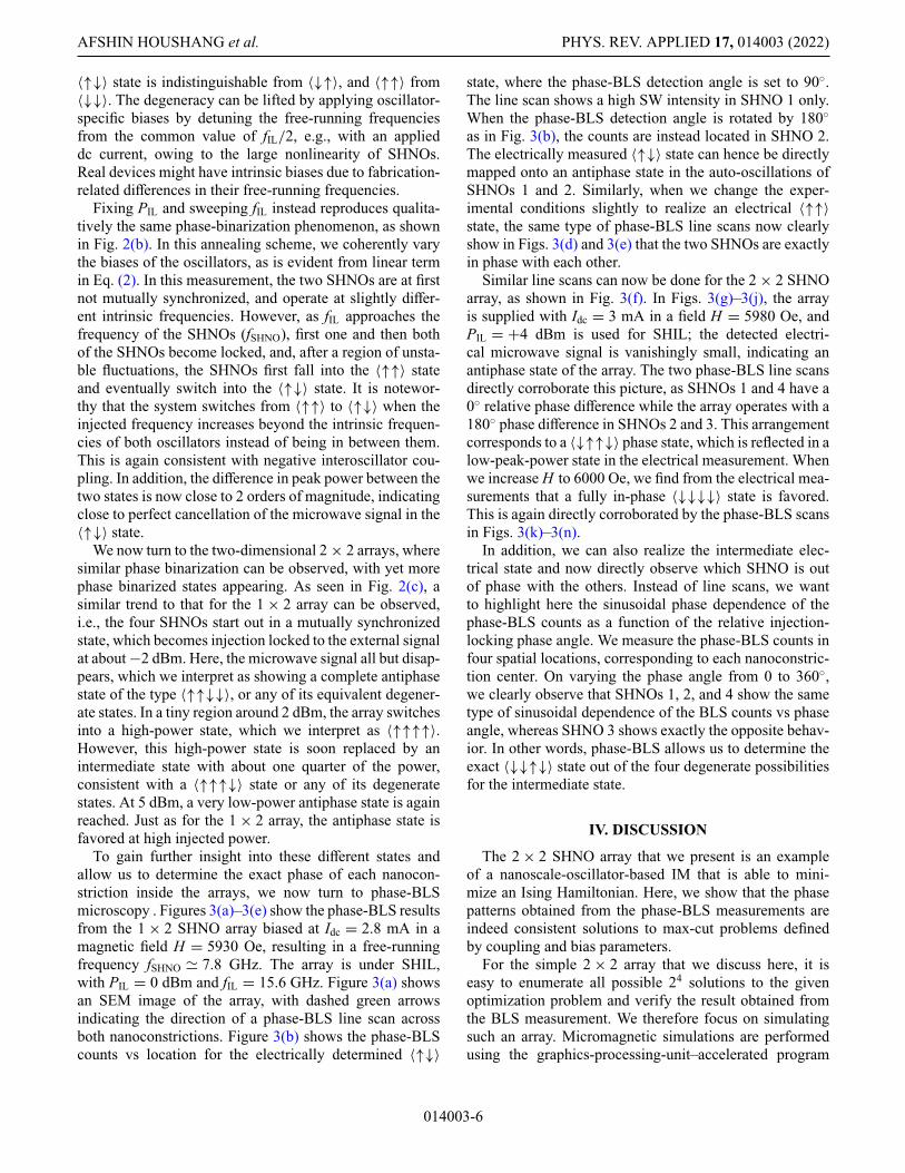
To gain further insight into these different states andallow us to determine the exact phase of each nanocon-striction inside the arrays, we now turn to phase-BLSmicroscopy . Figures 3(a)–3(e) show the phase-BLS resultsfrom the 1 × 2 SHNO array biased at Idc = 2.8 mA in amagnetic field H = 5930 Oe, resulting in a free-runningfrequency fSHNO � 7.8 GHz. The array is under SHIL,with PIL = 0 dBm and fIL = 15.6 GHz. Figure 3(a) showsan SEM image of the array, with dashed green arrowsindicating the direction of a phase-BLS line scan acrossboth nanoconstrictions. Figure 3(b) shows the phase-BLScounts vs location for the electrically determined 〈↑↓〉
state, where the phase-BLS detection angle is set to 90◦.The line scan shows a high SW intensity in SHNO 1 only.When the phase-BLS detection angle is rotated by 180◦as in Fig. 3(b), the counts are instead located in SHNO 2.The electrically measured 〈↑↓〉 state can hence be directlymapped onto an antiphase state in the auto-oscillations ofSHNOs 1 and 2. Similarly, when we change the exper-imental conditions slightly to realize an electrical 〈↑↑〉state, the same type of phase-BLS line scans now clearlyshow in Figs. 3(d) and 3(e) that the two SHNOs are exactlyin phase with each other.
Similar line scans can now be done for the 2 × 2 SHNOarray, as shown in Fig. 3(f). In Figs. 3(g)–3(j), the arrayis supplied with Idc = 3 mA in a field H = 5980 Oe, andPIL = +4 dBm is used for SHIL; the detected electri-cal microwave signal is vanishingly small, indicating anantiphase state of the array. The two phase-BLS line scansdirectly corroborate this picture, as SHNOs 1 and 4 have a0◦ relative phase difference while the array operates with a180◦ phase difference in SHNOs 2 and 3. This arrangementcorresponds to a 〈↓↑↑↓〉 phase state, which is reflected in alow-peak-power state in the electrical measurement. Whenwe increase H to 6000 Oe, we find from the electrical mea-surements that a fully in-phase 〈↓↓↓↓〉 state is favored.This is again directly corroborated by the phase-BLS scansin Figs. 3(k)–3(n).
In addition, we can also realize the intermediate elec-trical state and now directly observe which SHNO is outof phase with the others. Instead of line scans, we wantto highlight here the sinusoidal phase dependence of thephase-BLS counts as a function of the relative injection-locking phase angle. We measure the phase-BLS counts infour spatial locations, corresponding to each nanoconstric-tion center. On varying the phase angle from 0 to 360◦,we clearly observe that SHNOs 1, 2, and 4 show the sametype of sinusoidal dependence of the BLS counts vs phaseangle, whereas SHNO 3 shows exactly the opposite behav-ior. In other words, phase-BLS allows us to determine theexact 〈↓↓↑↓〉 state out of the four degenerate possibilitiesfor the intermediate state.
IV. DISCUSSION
The 2 × 2 SHNO array that we present is an exampleof a nanoscale-oscillator-based IM that is able to mini-mize an Ising Hamiltonian. Here, we show that the phasepatterns obtained from the phase-BLS measurements areindeed consistent solutions to max-cut problems definedby coupling and bias parameters.
For the simple 2 × 2 array that we discuss here, it iseasy to enumerate all possible 24 solutions to the givenoptimization problem and verify the result obtained fromthe BLS measurement. We therefore focus on simulatingsuch an array. Micromagnetic simulations are performedusing the graphics-processing-unit–accelerated program
014003-6

PHASE-BINARIZED SPIN HALL NANO-OSCILLATOR ARRAYS. . . PHYS. REV. APPLIED 17, 014003 (2022)
(a)
(b)
(d)
(f)
(g) (h)
(j)
(l)
(m) (n)
(o) (p)
(q) (r)
(k)
(i)
(e)
(c)
1x2 array
2x2 array
FIG. 3. Phase-resolved BLSmicroscopy of individual SHNOs.(a) SEM image of the 1 × 2SHNO array under study; thegreen arrow shows the directionof the BLS line scan. SHIL withPIL = 0 dBm and fIL = 15.6 GHzis used. (b)–(e) show the spinwave (SW) intensity profile of theSHNOs for the phase-resolvedBLS signal at 90◦ and 270◦. TheSHNOs in (b),(c) are energizedwith a 180◦ phase difference(〈↑↓〉) when 2fSHNO < fIL, and in(d),(e) with a 0◦ phase difference(〈↑↑〉) when 2fSHNO � fIL. (f)SEM image of a 2 × 2 SHNOarray with corresponding BLSline-scan directions. Phase-resolved BLS line scans areshown in (g)–(j) for PIL = +4dBm, corresponding to the〈↓↑↑↓〉 phase state, while (k)–(n)show the 〈↓↓↓↓〉 state obtainedat PIL = +3 dBm. (o)–(r) BLScounts for the least stable phasestate 〈↓↓↑↓〉 at PIL = −2 dBm,measured by sweeping the phase(ϕ) of the BLS.
MuMax3 [46]. The system geometry is obtained from thecomputer-aided-design model used during the nanofabri-cation process and discretized into 1024 × 1024 × 1 gridcells representing the Ni80Fe20 layer of the stack. Theindividual size of each cell is 4 × 4 × 3 nm. The currentand Oersted-field distributions are calculated separatelyand included in the simulation as a source of the spin
current originating from the spin Hall effect and as anexternal magnetic field, respectively. The parameters usedin the simulations are chosen to mimic the experimentalconditions as closely as possible, including a saturationmagnetization μ0MS = 0.59 T, a Gilbert damping constantα = 0.025, a spin Hall angle θSH = 0.09, and an exchangeconstant Aex = 10 pJ/m. The magnetic field is applied at
014003-7

AFSHIN HOUSHANG et al. PHYS. REV. APPLIED 17, 014003 (2022)
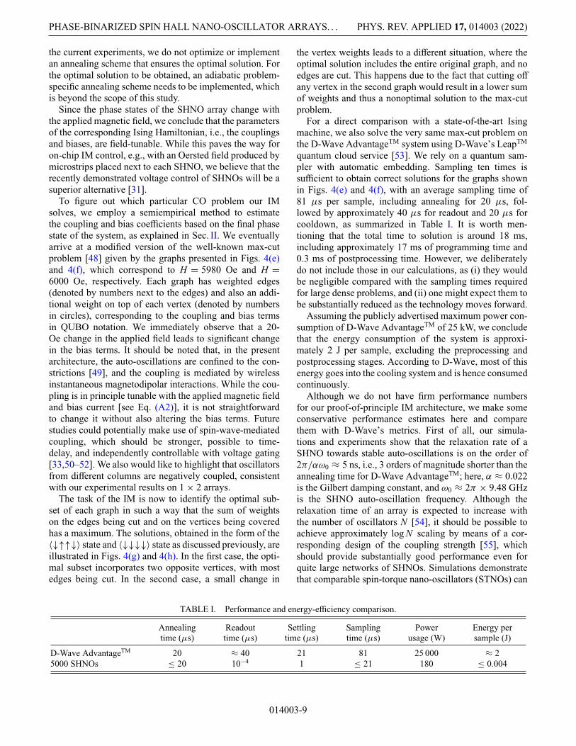
an angle of 78◦ to the sample plane and a 24◦ in-planeangle. Both the value of the dc current and the amplitudeof the ac binarization current are equal to 3 mA. Eachsimulation lasts 150 ns, where the first 50 ns are usedfor initialization of the magnetization dynamics withoutac excitation and the remaining 100 ns include the bina-rization current. FFT amplitude and phase diagrams areproduced based on the last 10 ns of each simulation, usingcustom software [47]. We first recreate the measurementresults using the method described above. After applyingan external magnetic field with a magnitude of 5980 Oeand a rf current with a frequency of 15.6 GHz, we observestable injection-locked oscillations at 7.8 GHz, which isclose to the natural frequency of the system. We then
perform a pointwise FFT on the simulated data and obtainthe spatially resolved amplitude and phase distributions ofthe auto-oscillation shown in Figs. 4(a) and 4(b), respec-tively. The amplitude map confirms that all four SHNOsauto-oscillate in the same type of mode, while one cansee a clear antiparallel 〈↓↑↑↓〉 phase pattern (the lowest-output-rf-power state) that is identical to the results ofthe phase-BLS measurements in Figs. 3(g)–3(j). A slightincrease in the applied field to 5990 Oe favors an interme-diate 〈↓↑↓↓〉 phase pattern [Fig. 4(c)], in agreement withFigs. 3(o)–3(r). Finally, increasing the field further to 6020Oe yields a spatially uniform 〈↓↓↓↓〉 phase state (with thehighest output rf power), as shown in Fig. 4(d), which isconsistent with Figs. 3(k)–3(n). It is worth noting that in
(a) (b)
(c)
(e) (f) (g) (h)
(d)
FIG. 4. Micromagnetic simulations of a 2 × 2 SHNO Ising machine. (a),(b) Spatial maps of the FFT amplitude and phase, respec-tively, obtained for a 7.8-GHz mode under a field H = 5980 Oe. Phase maps are also shown for H increased to 5990 Oe (c) and to6020 Oe (d), where the change in the Ising-problem parameters results in different phase patterns. The modified max-cut problemscorresponding to fields of 5980 Oe (e) and 6000 Oe (f) are also shown. By reading out the phase patterns of the SHNO network,optimal solutions to these problems are obtained, as illustrated in (g),(h).
014003-8
PHASE-BINARIZED SPIN HALL NANO-OSCILLATOR ARRAYS. . . PHYS. REV. APPLIED 17, 014003 (2022)
the current experiments, we do not optimize or implementan annealing scheme that ensures the optimal solution. Forthe optimal solution to be obtained, an adiabatic problem-specific annealing scheme needs to be implemented, whichis beyond the scope of this study.
Since the phase states of the SHNO array change withthe applied magnetic field, we conclude that the parametersof the corresponding Ising Hamiltonian, i.e., the couplingsand biases, are field-tunable. While this paves the way foron-chip IM control, e.g., with an Oersted field produced bymicrostrips placed next to each SHNO, we believe that therecently demonstrated voltage control of SHNOs will be asuperior alternative [31].
To figure out which particular CO problem our IMsolves, we employ a semiempirical method to estimatethe coupling and bias coefficients based on the final phasestate of the system, as explained in Sec. II. We eventuallyarrive at a modified version of the well-known max-cutproblem [48] given by the graphs presented in Figs. 4(e)and 4(f), which correspond to H = 5980 Oe and H =6000 Oe, respectively. Each graph has weighted edges(denoted by numbers next to the edges) and also an addi-tional weight on top of each vertex (denoted by numbersin circles), corresponding to the coupling and bias termsin QUBO notation. We immediately observe that a 20-Oe change in the applied field leads to significant changein the bias terms. It should be noted that, in the presentarchitecture, the auto-oscillations are confined to the con-strictions [49], and the coupling is mediated by wirelessinstantaneous magnetodipolar interactions. While the cou-pling is in principle tunable with the applied magnetic fieldand bias current [see Eq. (A2)], it is not straightforwardto change it without also altering the bias terms. Futurestudies could potentially make use of spin-wave-mediatedcoupling, which should be stronger, possible to time-delay, and independently controllable with voltage gating[33,50–52]. We also would like to highlight that oscillatorsfrom different columns are negatively coupled, consistentwith our experimental results on 1 × 2 arrays.
The task of the IM is now to identify the optimal sub-set of each graph in such a way that the sum of weightson the edges being cut and on the vertices being coveredhas a maximum. The solutions, obtained in the form of the〈↓↑↑↓〉 state and 〈↓↓↓↓〉 state as discussed previously, areillustrated in Figs. 4(g) and 4(h). In the first case, the opti-mal subset incorporates two opposite vertices, with mostedges being cut. In the second case, a small change in
TABLE I. Performance and energy-efficiency comparison.
Annealing Readout Settling Sampling Power Energy pertime (μs) time (μs) time (μs) time (μs) usage (W) sample (J)
D-Wave AdvantageTM 20 ≈ 40 21 81 25 000 ≈ 25000 SHNOs ≤ 20 10−4 1 ≤ 21 180 ≤ 0.004
the vertex weights leads to a different situation, where theoptimal solution includes the entire original graph, and noedges are cut. This happens due to the fact that cutting offany vertex in the second graph would result in a lower sumof weights and thus a nonoptimal solution to the max-cutproblem.
For a direct comparison with a state-of-the-art Isingmachine, we also solve the very same max-cut problem onthe D-Wave AdvantageTM system using D-Wave’s LeapTM
quantum cloud service [53]. We rely on a quantum sam-pler with automatic embedding. Sampling ten times issufficient to obtain correct solutions for the graphs shownin Figs. 4(e) and 4(f), with an average sampling time of81 μs per sample, including annealing for 20 μs, fol-lowed by approximately 40 μs for readout and 20 μs forcooldown, as summarized in Table I. It is worth men-tioning that the total time to solution is around 18 ms,including approximately 17 ms of programming time and0.3 ms of postprocessing time. However, we deliberatelydo not include those in our calculations, as (i) they wouldbe negligible compared with the sampling times requiredfor large dense problems, and (ii) one might expect them tobe substantially reduced as the technology moves forward.
Assuming the publicly advertised maximum power con-sumption of D-Wave AdvantageTM of 25 kW, we concludethat the energy consumption of the system is approxi-mately 2 J per sample, excluding the preprocessing andpostprocessing stages. According to D-Wave, most of thisenergy goes into the cooling system and is hence consumedcontinuously.
Although we do not have firm performance numbersfor our proof-of-principle IM architecture, we make someconservative performance estimates here and comparethem with D-Wave’s metrics. First of all, our simula-tions and experiments show that the relaxation rate of aSHNO towards stable auto-oscillations is on the order of2π/αω0 ≈ 5 ns, i.e., 3 orders of magnitude shorter than theannealing time for D-Wave AdvantageTM; here, α ≈ 0.022is the Gilbert damping constant, and ω0 ≈ 2π × 9.48 GHzis the SHNO auto-oscillation frequency. Although therelaxation time of an array is expected to increase withthe number of oscillators N [54], it should be possible toachieve approximately log N scaling by means of a cor-responding design of the coupling strength [55], whichshould provide substantially good performance even forquite large networks of SHNOs. Simulations demonstratethat comparable spin-torque nano-oscillators (STNOs) can
014003-9
AFSHIN HOUSHANG et al. PHYS. REV. APPLIED 17, 014003 (2022)
anneal a max-cut problem with 288 variables in around450 ns with a probability of 50% of achieving an opti-mal solution in 100 samples [45]. Moreover in Ref. [56],a simulated array of 2500 STNOs was able to fully syn-chronize on a timescale of around 1.5 μs even without asophisticated annealing scheme. Therefore, we are confi-dent that large-scale SHNO arrays could perform adiabaticannealing at least on a par with the time for D-WaveAdvantageTM, which is generally problem-specific [17]but defaults to 20 μs. We then ultimately aim for on-chip real-time measurements of the phases of the SHNOs.Assuming that the electronic front end, including low-noise amplifiers, current sources, and digital logic, worksat the same frequencies as the SHNOs, e.g., by using asilicon-on-insulator process, we would expect a readouttime of 2π/ω0 = 100 ps. Now, for the power consumptionper SHNO, we take into account a value for the Joule heat-ing of a SHNO PSHNO = I 2
biasRSHNO = 2.25 mW, whereIbias = 3 mA is the bias current and RSHNO ≈ 250 � is thetypical dc resistance of a 120-nm SHNO, and an injectedrf power of around 1 mW, giving 3.25 mW in total. Ifwe assume that the on-chip electronic front end consumesan order of magnitude more than the SHNO itself does,we arrive at a power consumption per “spin” of around36 mW. Assuming that the dc and rf power consump-tions scale linearly with the number of oscillators in thearray, we expect 180 W consumption for a system of 5000“spins.” This is within the range of the current genera-tion of Peltier elements, and so we expect the postreadoutcooling to be as fast as the spin-lattice relaxation time,which typically lies in the picosecond to nanosecond range.So, we finally arrive at a sampling time of 21 μs and anenergy consumption of 0.0038 J per sample. While thisnumber is already about 500 times smaller than that for theD-Wave AdvantageTM system, there is significant furtherpotential for an additional 1–2 orders of magnitude lowerenergy consumption via both a reduction of the SHNOthreshold current and an increase in the SHNO operationalfrequency [30,31,57]. It is also worth pointing out thatour SHNO architecture consumes energy only on demand,i.e., during sampling, since it does not require an always-on cryogenic cooling system. We therefore believe that,compared with D-Wave’s AdvantageTM system, our archi-tecture holds significant promise for substantially reducedpower consumption, faster sampling, and a substantiallysmaller footprint.
As SHNO arrays as large as 10 × 10 have been shownto be fully operational with strong interoscillator cou-pling, we argue that it should be possible to scale up ourpresent demonstration to very large arrays. We also believethat voltage-controlled magnetic anisotropy in Co-Fe-B-based SHNOs [33] could be a possible route towards afully integrated voltage-controlled SHNO Ising machine.For fast electrical readout, one could also add magnetictunnel junctions to the auto-oscillating regions of each
nanoconstriction. While these are important challenges,the very high operating frequency, the very high degreeof miniaturization, the demonstrated scaling path, and theCMOS compatibility all hold tremendous promise for agroundbreaking technology platform aimed towards wide-purpose Ising machines.
ACKNOWLEDGMENTS
This work was partially supported by the Horizon 2020research and innovation program (ERC Advanced GrantNo. 835068, “TOPSPIN”). This work was also partiallysupported by the Swedish Research Council (VR) and theKnut and Alice Wallenberg Foundation. J.Ch. acknowl-edges funding from Program No. 2017/24/T/ST3/00009of the National Science Center, Poland. The numericalcalculations were supported in part by the PL-Grid infras-tructure. We acknowledge D-Wave Systems Inc. for pro-viding developers, researchers, and academics with accessto quantum computing technology via their cloud serviceLeapTM.
APPENDIX: ISING-HAMILTONIANCALCULATIONS AND MODIFIED MAX-CUT
PROBLEM
Based on the results of the micromagnetic simulations,we can expect the oscillation mode in the Pt/Ni80Fe20bilayer to be localized near the constriction area. There-fore, we neglect the exchange-mediated contribution tothe coupling and focus only on the magnetodipolar con-tribution. Assuming that all oscillators in the array haveidentical physical parameters and taking into account thevectorial structure of the precession in the applied field[50,58], we expect that the coupling strength Jij betweenthe ith and j th oscillators will be given by
Jij =√
1 + ν2 Veff
aij3
γ 2MS
2ω0
[H
(3 sin2 θ cos2 φij − 1
)
+ MS sin2 θ(1 − 3 sin2 φij
)]. (A1)
Here, ν is the normalized nonlinear frequency-shift coef-ficient, Veff is the effective oscillator volume, aij is thedistance between two oscillators, γ is the gyromagneticratio, ω0 is the generated frequency, θ is the angle betweenthe external magnetic field H and the sample plane, and φijis the angle between the in-plane component of the exter-nal magnetic field and the line connecting the ith and j thoscillators. For the purpose of Ising-machine calculations,it is convenient to introduce a constant factor J0 that isapproximately the same for all oscillators in the array:
J0 =√
1 + ν2 Veff
a03
γ 2MS
2ω0H , (A2)
014003-10

PHASE-BINARIZED SPIN HALL NANO-OSCILLATOR ARRAYS. . . PHYS. REV. APPLIED 17, 014003 (2022)
where a0 is the pitch size of the array, equal to 300 nm.This allows us to express the individual Jij values as
Jij = J0
(a0
aij
)3 (3 sin2 θ cos2 φij − 1
+ MS
Hsin2 θ
(1 − 3 sin2 φij
)). (A3)
For the parameters used in our system, we expect J0 tobe of the order of magnitude of 50–200 MHz, which isalso consistent with our micromagnetic simulations. Inorder to obtain the best fit with the experiment, from nowon we assume J0 = 87 MHz. To calculate the values ofJij , we now take into account the nonsymmetrical geom-etry of our system, and find that a12 = a34 = 300 nm,a13 = a24 ≈ 305 nm, a23 ≈ 385 nm, a14 ≈ 467 nm, φ12 =φ34 = 24◦, φ13 = φ24 = 77◦, φ23 = 27◦, and φ14 = 117◦.From this, we calculate J12 = J34 = 1.87J0, J13 = J24 =−2.47J0, J23 = 0.77J0, and J14 = −0.46J0.
As a result, the Lyapunov function minimized by theSHNO array [19] can be written as
E( �φ) = −N∑
i=1
N∑
j �=i
Jij cos(φi − φj ) −N∑
i=1
2fi − finj
fiφi.
(A4)
Here, we neglect the binarization term for simplicity, sincewe focus on states that are already binarized, and intro-duce dimensionless coupling coefficients Jij = KJij , whereK is an arbitrary scaling factor having units of time. Underthe working conditions of our system, the oscillator phasesare locked by the injected rf signal, which allows us torewrite the previous equation in a more practical QUBOform, assuming φi = πxi and cos πxi = 1 − 2xi:
E(�x) = −N∑
i=1
N∑
j �=i
4Jij xixj
+N∑
i=1
⎡
⎣N∑
j �=i
2Jij − π(2fi − finj)
fi
⎤
⎦ xi, (A5)
where constant terms are omitted and the xi ∈ 0, 1 arevariables in the binary optimization problem. The SHNO-based Ising machine works by minimizing the expressionin Eq. (A5) in such a way that the resulting oscillatorphases, when equal to 0 or π , correspond to the variablesxi being equal to either 0 or 1.
We also perform a set of additional micromagnetic sim-ulations with no spin Hall effect present and find that, dueto the geometrical asymmetry of the array, the effectivefield in the area of nanoconstrictions 1 and 4 is higherthan the effective field in the area of nanoconstrictions 2
and 3 by approximately 50 Oe. We assume that this dif-ference persists under spin-Hall-excitation conditions andleads to a difference in free-running frequencies betweenoscillators 1 and 4 on the one hand and oscillators 2 and3 on the other equal to approximately 140 MHz. Aftersupplying the array with 3 mA of dc current but no ac cur-rent, we find the frequency of the entire array to be 7.87GHz for H = 5980 Oe and 7.90 GHz for H = 6000 Oe.Therefore, we assume that the values of fi in Eq. (A5) aref1 = f4 = 7.80 GHz and f2 = f3 = 7.94 GHz for H = 5980Oe, and f1 = f4 = 7.83 GHz and f2 = f3 = 7.97 GHz forH = 6000 Oe. The frequency of the injected binarizationcurrent remains the same in both cases and is equal tofinj = 15.60 GHz. As the external magnetic field amplitudeincreases, it can potentially affect not only the values of fibut also those of Jij . We calculate this effect using the sameassumptions for J0 as previously and find that it remainsnegligible compared with the changes in fi, which is whywe do not include it in the analysis.
To obtain a formulation of a max-cut problem for oursystem, we rewrite Eq. (A5) as
E(�x) =N∑
i=1
N∑
j �=i
wij (2xixj − xi − xj ) −N∑
i=1
oixi, (A6)
where wij = −2Jij and oi = π(2fi − finj)/fi. The aboveterm describes the Lyapunov function that is minimized bythe Ising machine. Since max-cut problems are typicallyformulated in terms of maximization and not minimiza-tion, we replace the expression above with an expressionthat the Ising machine will maximize:
E(�x) = −E(�x) =N∑
i=1
N∑
j �=i
wij (xi + xj − 2xixj ) +N∑
i=1
oixi.
(A7)
Now, we notice that the term xi + xj − 2xixj describesthe edge-cutting procedure in the classical max-cutproblem [48]. If xi = xj (both vertices are in the samesubset) then the term vanishes, and if xi �= xj (the ver-tices belong to opposite subsets, i.e., the edge betweenthem is cut) then the term is equal to 1. Therefore, wecan use this expression to evaluate possible subset cuts ina weighted graph with the wij serving as weights. Addi-tionally, the expression in Eq. (A7) includes a term thatpunishes (or rewards, depending on the sign of oi) a pro-posed way of cutting for assigning a particular vertex tothe subset denoted by xi equal to 1. We also note here that,for the sake of convenience, the wij and oi values shownin Figs. 4(e)–4(h) are rounded and rescaled by a con-stant factor of 200, which does not affect the maximizationprocedure.
014003-11

AFSHIN HOUSHANG et al. PHYS. REV. APPLIED 17, 014003 (2022)
[1] E. Lawler, Combinatorial Optimization - Networks andMatroids (Holt, Rinehart and Winston, New York, 1976).
[2] F. Glover, G. Kochenberger, and Y. Du, A tutorial onformulating and using QUBO models (2019).
[3] A. Lucas, Ising formulations of many NP problems, Front.Phys. 2, 5 (2014).
[4] S. Jiang, K. A. Britt, A. J. McCaskey, T. S. Humble, andS. Kais, Quantum annealing for prime factorization, Sci.Rep. 8, 17667 (2018).
[5] B. Wang, F. Hu, H. Yao, and C. Wang, Prime factorizationalgorithm based on parameter optimization of ising model,Sci. Rep. 10, 7106 (2020).
[6] E. Farhi, J. Goldstone, S. Gutmann, J. Lapan, A. Lundgren,and D. Preda, A quantum adiabatic evolution algorithmapplied to random instances of an NP-complete problem,Science 292, 472 (2001).
[7] S. Boixo, T. F. Rønnow, S. V. Isakov, Z. Wang, D. Wecker,D. A. Lidar, J. M. Martinis, and M. Troyer, Evidence forquantum annealing with more than one hundred qubits, Nat.Phys. 10, 218 (2014).
[8] S. Tsukamoto, M. Takatsu, S. Matsubara, and H. Tamura,An accelerator architecture for combinatorial optimizationproblems, Fujitsu Sci. Tech. J. 53, 8 (2017).
[9] M. Yamaoka, C. Yoshimura, M. Hayashi, T. Okuyama,H. Aoki, and H. Mizuno, in 2015 IEEE International Solid-State Circuits Conference-(ISSCC) Digest of TechnicalPapers (IEEE, 2015), p. 1.
[10] D. Oku, K. Terada, M. Hayashi, M. Yamaoka, S. Tanaka,and N. Togawa, A fully-connected ising model embeddingmethod and its evaluation for CMOS annealing machines,IEICE Trans. Inf. Syst. 102, 1696 (2019).
[11] B. Sutton, K. Y. Camsari, B. Behin-Aein, and S. Datta,Intrinsic optimization using stochastic nanomagnets, Sci.Rep. 7, 44370 (2017).
[12] A. Parihar, N. Shukla, M. Jerry, S. Datta, and A. Ray-chowdhury, Vertex coloring of graphs via phase dynam-ics of coupled oscillatory networks, Sci. Rep. 7, 911(2017).
[13] J. Chou, S. Bramhavar, S. Ghosh, and W. Herzog, Analogcoupled oscillator based weighted ising machine, Sci. Rep.9, 1 (2019).
[14] C. Roques-carmes, Y. Shen, L. Jing, T. Dubcek,S. A. Skirlo, H. Bagherianlemraski, and M. Soljacic, Opti-cal Ising machines and optical convolutional neural net-works (2019), uS Patent App. 16/032, 737.
[15] Y. Yamamoto, K. Aihara, T. Leleu, K.-i. Kawarabayashi,S. Kako, M. Fejer, K. Inoue, and H. Takesue, Coherentising machines: Optical neural networks operating at thequantum limit, Npj Quantum Inf. 3, 49 (2017).
[16] A. Marandi, Z. Wang, K. Takata, R. L. Byer, andY. Yamamoto, Network of time-multiplexed optical para-metric oscillators as a coherent ising machine, Nat. Photon-ics 8, 937 (2014).
[17] R. Hamerly, T. Inagaki, P. L. McMahon, D. Venturelli,A. Marandi, T. Onodera, E. Ng, C. Langrock, K. Inaba, andT. Honjo et al., Experimental investigation of performancedifferences between coherent Ising machines and a quantumannealer, Sci. Adv. 5, eaau0823 (2019).
[18] J. Boyd, Silicon chip delivers quantum speeds [news], IEEESpectr. 55, 10 (2018).
[19] T. Wang and J. Roychowdhury, in International Conferenceon Unconventional Computation and Natural Computation(Springer, 2019), p. 232.
[20] A. M. Lyapunov, The general problem of the stability ofmotion, Int. J. Control. 55, 531 (1992).
[21] R. Adler, A study of locking phenomena in oscillators,Proceedings of the IRE 34, 351 (1946).
[22] P. Bhansali and J. Roychowdhury, in 2009 Asia and SouthPacific Design Automation Conference (2009), p. 522.
[23] A. Neogy and J. Roychowdhury, in 2012 Design, Automa-tion Test in Europe Conference Exhibition (DATE) (2012),p. 1209.
[24] T. Wang, L. Wu, and J. Roychowdhury, in Proceedingsof the 56th Annual Design Automation Conference 2019(2019), p. 1.
[25] V. E. Demidov, S. Urazhdin, A. Zholud, A. V. Sadovnikov,and S. O. Demokritov, Nanoconstriction-based spin-hallnano-oscillator, Appl. Phys. Lett. 105, 172410 (2014).
[26] M. Ranjbar, P. Dürrenfeld, M. Haidar, E. Iacocca, M. Balin-skiy, T. Le, M. Fazlali, A. Houshang, A. Awad, R. Dumas,and J. Åkerman, CoFeB-based spin Hall nano-oscillators,IEEE Magn. Lett. 5, 3000504 (2014).
[27] T. Chen, R. K. Dumas, A. Eklund, P. K. Muduli,A. Houshang, A. A. Awad, P. Dürrenfeld, B. G. Malm,A. Rusu, and J. Åkerman, Spin-torque and spin-hall nano-oscillators, Proc. IEEE 104, 1919 (2016).
[28] R. H. Liu, W. L. Lim, and S. Urazhdin, Spectral Char-acteristics of the Microwave Emission by the Spin HallNano-Oscillator, Phys. Rev. Lett. 110, 147601 (2013).
[29] V. E. Demidov, S. Urazhdin, H. Ulrichs, V. Tiberkevich,A. Slavin, D. Baither, G. Schmitz, and S. O. Demokritov,Magnetic nano-oscillator driven by pure spin current, Nat.Mater. 11, 1028 (2012).
[30] M. Zahedinejad, H. Mazraati, H. Fulara, J. Yue, S. Jiang,A. A. Awad, and J. Åkerman, CMOS compatibleW/CoFeB/MgO spin Hall nano-oscillators with wide fre-quency tunability, Appl. Phys. Lett. 112, 132404 (2018).
[31] H. Fulara, M. Zahedinejad, R. Khymyn, M. Dvornik,S. Fukami, S. Kanai, H. Ohno, and J. Åkerman, Giantvoltage-controlled modulation of spin Hall nano-oscillatordamping, Nat. Commun. 11, 4006 (2020).
[32] M. Haidar, A. A. Awad, M. Dvornik, R. Khymyn,A. Houshang, and J. Åkerman, A single layer spin-orbittorque nano-oscillator, Nat. Commun. 10, 2362 (2019).
[33] H. Fulara, M. Zahedinejad, R. Khymyn, A. A. Awad,S. Muralidhar, M. Dvornik, and J. Åkerman, Spin-orbit torque–driven propagating spin waves, Sci. Adv. 5,eaax8467 (2019).
[34] A. Awad, A. Houshang, M. Zahedinejad, R. Khymyn, andJ. Åkerman, Width dependent auto-oscillating properties ofconstriction based spin Hall nano-oscillators, Appl. Phys.Lett. 116, 232401 (2020).
[35] H. Mazraati, M. Zahedinejad, and J. Åkerman, Improv-ing the magnetodynamical properties of NiFe/Pt bilay-ers through Hf dusting, Appl. Phys. Lett. 113, 092401(2018).
[36] M. Zahedinejad, A. A. Awad, P. Dürrenfeld, A. Houshang,Y. Yin, P. K. Muduli, and J. Åkerman, Current modulationof nanoconstriction spin-hall nano-oscillators, IEEE Magn.Lett. 8, 3704804 (2017).
014003-12
PHASE-BINARIZED SPIN HALL NANO-OSCILLATOR ARRAYS. . . PHYS. REV. APPLIED 17, 014003 (2022)
[37] T. Kendziorczyk and T. Kuhn, Mutual synchronization ofnanoconstriction-based spin Hall nano-oscillators throughevanescent and propagating spin waves, Phys. Rev. B 93,134413 (2016).
[38] A. A. Awad, P. Dürrenfeld, A. Houshang, M. Dvornik,E. Iacocca, R. K. Dumas, and J. Åkerman, Long-rangemutual synchronization of spin Hall nano-oscillators, Nat.Phys. 13, 292 (2017).
[39] V. E. Demidov, H. Ulrichs, S. V. Gurevich, S. O. Demokri-tov, V. S. Tiberkevich, A. N. Slavin, A. Zholud, and S.Urazhdin, Synchronization of spin Hall nano-oscillators toexternal microwave signals, Nat. Commun. 5, 3179 (2014).
[40] T. Hache, T. Weinhold, K. Schultheiss, J. Stigloher, F.Vilsmeier, C. Back, S. S. Arekapudi, O. Hellwig, J. Fass-bender, and H. Schultheiss, Combined frequency and timedomain measurements on injection-locked, constriction-based spin Hall nano-oscillators, Appl. Phys. Lett. 114,102403 (2019).
[41] L. Yang, R. Verba, V. Tiberkevich, T. Schneider, A. Smith,Z. Duan, B. Youngblood, K. Lenz, J. Lindner, A. N. Slavin,and I. N. Krivorotov, Reduction of phase noise in nanowirespin orbit torque oscillators, Sci. Rep. 5, 16942 (2015).
[42] C. Roques-Carmes, Y. Shen, C. Zanoci, M. Prabhu,F. Atieh, L. Jing, T. Dubcek, C. Mao, M. R. Johnson, V.Ceperic, J. D. Joannopoulos, D. Englund, and M. Soljacic,Heuristic recurrent algorithms for photonic ising machines,Nat. Commun. 11, 249 (2020).
[43] P. Dürrenfeld, A. A. Awad, A. Houshang, R. K. Dumas, andJ. Åkerman, A 20 nm spin Hall nano-oscillator, Nanoscale9, 1285 (2017).
[44] M. Zahedinejad, A. A. Awad, S. Muralidhar, R. Khymyn,H. Fulara, H. Mazraati, M. Dvornik, and J. Åkerman,Two-dimensional mutually synchronized spin Hall nano-oscillator arrays for neuromorphic computing, Nat. Nan-otech. 15, 47 (2020).
[45] D. I. Albertsson, M. Zahedinejad, A. Houshang, R. Khymyn,J. Åkerman, and A. Rusu, Ultrafast Ising machines usingspin torque nano-oscillators, Appl. Phys. Lett. 118, 112404(2021).
[46] A. Vansteenkiste, J. Leliaert, M. Dvornik, M. Helsen,F. Garcia-Sanchez, and B. Van Waeyenberge, The designand verification of MuMax3, AIP Adv. 4, 107133(2014).
[47] M. Frankowski, J. Checinski, and M. Czapkiewicz, Spatialspectrum analyzer (SSA): A tool for calculations of spatial
distribution of fast Fourier transform spectrum from objectoriented micromagnetic framework output data, Comput.Phys. Commun. 189, 207 (2015).
[48] F. Glover, G. Kochenberger, and Y. Du, Quantum bridgeanalytics i: A tutorial on formulating and using QUBOmodels, 4OR 17, 335 (2019).
[49] M. Dvornik, A. A. Awad, and J. Åkerman, Originof Magnetization Auto-Oscillations in Constriction-BasedSpin Hall Nano-Oscillators, Phys. Rev. Appl. 9, 014017(2018).
[50] A. N. Slavin and V. S. Tiberkevich, Theory of mutual phaselocking of spin-torque nanosized oscillators, Phys. Rev. B74, 104401 (2006).
[51] H. Fulara, M. Zahedinejad, R. Khymyn, M. Dvornik,S. Fukami, S. Kanai, H. Ohno, and J. Akerman, Strongvoltage-induced tunability of threshold current and fre-quency in spin Hall nano-oscillators, Bulletin of the Amer-ican Physical Society (2020).
[52] M. Zahedinejad, H. Fulara, R. Khymyn, A. Houshang,S. Fukami, S. Kanai, H. Ohno, and J. Åkerman, Memristivecontrol of mutual SHNO synchronization for neuromorphiccomputing (2020).
[53] M. Dvornik, An example of simple Max − Cut problemsolved with D − WaveLeapQuantumCloudService (2021).
[54] J. Wu and X. Li, Finite-time and fixed-time synchroniza-tion of Kuramoto-oscillator network with multiplex control,IEEE Trans Control Netw. Syst. 6, 863 (2019).
[55] S.-W. Son, H. Jeong, and H. Hong, Relaxation of synchro-nization on complex networks, Phys. Rev. E 78, 016106(2008).
[56] V. Flovik, F. Macià, and E. Wahlström, Describing synchro-nization and topological excitations in arrays of magneticspin torque oscillators through the Kuramoto model, Sci.Rep. 6, 32528 (2016).
[57] H. Mazraati, S. Chung, A. Houshang, M. Dvornik,L. Piazza, F. Qejvanaj, S. Jiang, T. Q. Le, J. Weissenrieder,and J. Åkerman, Low operational current spin Hall nano-oscillators based on NiFe/W bilayers, Appl. Phys. Lett. 109,242402 (2016).
[58] A. Slavin and V. Tiberkevich, Nonlinear auto-oscillatortheory of microwave generation by spin-polarized current,Magn. IEEE Trans. 45, 1875 (2009).
Correction: The author order was set incorrectly and has been fixed.
014003-13