IST-LASAGNE: Towards all-optical label swapping employing optical logic gates and optical flip-flops
19
JOURNAL OF LIGHTWAVE TECHNOLOGY, VOL. 23, NO. 10, OCTOBER 2005 2993 IST-LASAGNE: Towards All-Optical Label Swapping Employing Optical Logic Gates and Optical Flip-Flops F. Ramos, Member, IEEE, E. Kehayas, J. M. Martinez, R. Clavero, J. Marti, Member, IEEE, L. Stampoulidis, D. Tsiokos, H. Avramopoulos, J. Zhang, P. V. Holm-Nielsen, N. Chi, P. Jeppesen, Member, IEEE, N. Yan, I. Tafur Monroy, A. M. J. Koonen, M. T. Hill, Y. Liu, H. J. S. Dorren, Member, IEEE, R. Van Caenegem, D. Colle, Member, IEEE, M. Pickavet, Member, IEEE, and B. Riposati, Member, IEEE Abstract—The Information Society Technologies—all-optical LAbel SwApping employing optical logic Gates in NEtwork nodes (IST-LASAGNE) project aims at designing and implementing the first, modular, scalable, and truly all-optical photonic router capable of operating at 40 Gb/s. The results of the first project year are presented in this paper, with emphasis on the implementation of network node functionalities employing optical logic gates and optical flip-flops, as well as the definition of the network architec- ture and migration scenarios. Index Terms—All-optical label swapping, all-optical logic gates, all-optical signal processing, Mach–Zehnder interferometer, optical flip-flops, optical packet switching, semiconductor optical amplifier, ultrafast nonlinear interferometer. I. I NTRODUCTION T HE huge growth of Internet traffic during the last years is forcing next-generation Internet protocol (IP) networks to increase their capacity, performance, and packet forwarding rates. Future IP-based all-optical networks will require tech- nologies to enable packet routing at terabit per second bit rates, supporting new streamlined IP routing protocols such as multiprotocol label swapping (MPLS) [1]. Optical network node implementations reported so far perform label packet processing in the electrical domain using alternative modula- tion formats or subcarrier multiplexing at lower bit rates (for example, IST-Switching Technologies for Optically LAbeled Manuscript received December 1, 2004. The European Commission is grate- fully acknowledged for partial funding of the IST-2004-507509 LASAGNE project in the 6th Framework Program. F. Ramos, J. M. Martinez, R. Clavero, and J. Marti are with the Nanophoton- ics Technology Center, Universidad Politécnica de Valencia, Valencia 46022, Spain (e-mail: [email protected]). E. Kehayas, L. Stampoulidis, D. Tsiokos, and H. Avramopoulos are with the Department of Electrical and Computer Engineering, National Technical University of Athens, Zographou, Athens 15773, Greece. J. Zhang, P. V. Holm-Nielsen, N. Chi, and P. Jeppesen are with the Research Center COM, Technical University of Denmark, DK 2800 Kgs. Lyngby, Denmark. N. Yan, I. Tafur Monroy, A. M. J. Koonen, M. T. Hill, Y. Liu, and H. J. S. Dorren are with the COBRA Research Institute, Eindhoven University of Technology, Eindhoven 5600 MB, The Netherlands. R. Van Caenegem, D. Colle, and M. Pickavet are with the Department of Information Technology, Ghent University, Gent 9000, Belgium. B. Riposati is with the Department of Network Innovation, Optical Network and Planning, Telecom Italia Lab, Torino I-10148, Italy. Digital Object Identifier 10.1109/JLT.2005.855714 Signals (STOLAS) [2] or IST-Light wave Architectures for the processing of Broadband ELectronic Signals (LABELS) [3] projects) through hybrid optoelectronic node architectures. However, in order to achieve high data-rate operation [4], packet-format transparency [5], and high transmission effi- ciency, all network node functionalities such as switching, rout- ing, and forwarding must be carried out directly in the physical layer. Likewise, the node optical layer needs to implement the required “intelligence” to look up the routing table and forward the packets. All-optical label swapping (AOLS) has been proposed as a viable approach towards resolving the mismatch between fiber transmission capacity and router packet forwarding capacity [6]. In such an AOLS scenario, all packet-by-packet routing and forwarding functions of MPLS are implemented directly in the optical domain. By using optical labels, the IP packets are directed through the core optical network without requiring O/E/O conversions whenever a routing decision is necessary. The main advantage of this approach is the ability to route pack- ets/bursts independently of bit rate, packet format, and packet length, increasing network flexibility and granularity, attri- butes highly desirable in broadband networks characterized by bandwidth-on-demand applications. In addition, compared to previous node implementations [2], [3], [7], the all-optical network node must be capable of operating with in-band serial- bit label signaling at the line rate, attaining high bandwidth utilization and simplified transmitter implementation. The abil- ity to process labels at the line rate through all-optical tech- niques eliminates the necessity for O/E/O conversions and allows for high information capacity to be encapsulated in the labels compared to lower-bit rate approaches [6]. Further, the labels are generated with the same light sources and inten- sity modulators as the payload [8], a major requirement for implementation of next-generation truly all-optical networks. In this paper, we present all-optical LAbel SwApping employing optical logic Gates in NEtwork nodes (LASAGNE), a novel node and network architecture based on AOLS scenario. The LASAGNE project aims at designing and implementing the first, modular, scalable, and truly all-optical photonic router capable of operating at 40 Gb/s. LASAGNE objectives in- clude studying, proposing, and validating the use of all-optical logic gates based on commercially available technologies to 0733-8724/$20.00 © 2005 IEEE
-
Upload
independent -
Category
Documents
-
view
3 -
download
0
Transcript of IST-LASAGNE: Towards all-optical label swapping employing optical logic gates and optical flip-flops

JOURNAL OF LIGHTWAVE TECHNOLOGY, VOL. 23, NO. 10, OCTOBER 2005 2993
IST-LASAGNE: Towards All-Optical LabelSwapping Employing Optical Logic Gates
and Optical Flip-FlopsF. Ramos, Member, IEEE, E. Kehayas, J. M. Martinez, R. Clavero, J. Marti, Member, IEEE, L. Stampoulidis,D. Tsiokos, H. Avramopoulos, J. Zhang, P. V. Holm-Nielsen, N. Chi, P. Jeppesen, Member, IEEE, N. Yan,I. Tafur Monroy, A. M. J. Koonen, M. T. Hill, Y. Liu, H. J. S. Dorren, Member, IEEE, R. Van Caenegem,
D. Colle, Member, IEEE, M. Pickavet, Member, IEEE, and B. Riposati, Member, IEEE
Abstract—The Information Society Technologies—all-opticalLAbel SwApping employing optical logic Gates in NEtwork nodes(IST-LASAGNE) project aims at designing and implementingthe first, modular, scalable, and truly all-optical photonic routercapable of operating at 40 Gb/s. The results of the first project yearare presented in this paper, with emphasis on the implementationof network node functionalities employing optical logic gates andoptical flip-flops, as well as the definition of the network architec-ture and migration scenarios.
Index Terms—All-optical label swapping, all-optical logicgates, all-optical signal processing, Mach–Zehnder interferometer,optical flip-flops, optical packet switching, semiconductor opticalamplifier, ultrafast nonlinear interferometer.
I. INTRODUCTION
THE huge growth of Internet traffic during the last yearsis forcing next-generation Internet protocol (IP) networks
to increase their capacity, performance, and packet forwardingrates. Future IP-based all-optical networks will require tech-nologies to enable packet routing at terabit per second bitrates, supporting new streamlined IP routing protocols suchas multiprotocol label swapping (MPLS) [1]. Optical networknode implementations reported so far perform label packetprocessing in the electrical domain using alternative modula-tion formats or subcarrier multiplexing at lower bit rates (forexample, IST-Switching Technologies for Optically LAbeled
Manuscript received December 1, 2004. The European Commission is grate-fully acknowledged for partial funding of the IST-2004-507509 LASAGNEproject in the 6th Framework Program.
F. Ramos, J. M. Martinez, R. Clavero, and J. Marti are with the Nanophoton-ics Technology Center, Universidad Politécnica de Valencia, Valencia 46022,Spain (e-mail: [email protected]).
E. Kehayas, L. Stampoulidis, D. Tsiokos, and H. Avramopoulos are withthe Department of Electrical and Computer Engineering, National TechnicalUniversity of Athens, Zographou, Athens 15773, Greece.
J. Zhang, P. V. Holm-Nielsen, N. Chi, and P. Jeppesen are with the ResearchCenter COM, Technical University of Denmark, DK 2800 Kgs. Lyngby,Denmark.
N. Yan, I. Tafur Monroy, A. M. J. Koonen, M. T. Hill, Y. Liu, andH. J. S. Dorren are with the COBRA Research Institute, Eindhoven Universityof Technology, Eindhoven 5600 MB, The Netherlands.
R. Van Caenegem, D. Colle, and M. Pickavet are with the Department ofInformation Technology, Ghent University, Gent 9000, Belgium.
B. Riposati is with the Department of Network Innovation, Optical Networkand Planning, Telecom Italia Lab, Torino I-10148, Italy.
Digital Object Identifier 10.1109/JLT.2005.855714
Signals (STOLAS) [2] or IST-Light wave Architectures forthe processing of Broadband ELectronic Signals (LABELS)[3] projects) through hybrid optoelectronic node architectures.However, in order to achieve high data-rate operation [4],packet-format transparency [5], and high transmission effi-ciency, all network node functionalities such as switching, rout-ing, and forwarding must be carried out directly in the physicallayer. Likewise, the node optical layer needs to implement therequired “intelligence” to look up the routing table and forwardthe packets.
All-optical label swapping (AOLS) has been proposed as aviable approach towards resolving the mismatch between fibertransmission capacity and router packet forwarding capacity[6]. In such an AOLS scenario, all packet-by-packet routingand forwarding functions of MPLS are implemented directlyin the optical domain. By using optical labels, the IP packetsare directed through the core optical network without requiringO/E/O conversions whenever a routing decision is necessary.The main advantage of this approach is the ability to route pack-ets/bursts independently of bit rate, packet format, and packetlength, increasing network flexibility and granularity, attri-butes highly desirable in broadband networks characterizedby bandwidth-on-demand applications. In addition, comparedto previous node implementations [2], [3], [7], the all-opticalnetwork node must be capable of operating with in-band serial-bit label signaling at the line rate, attaining high bandwidthutilization and simplified transmitter implementation. The abil-ity to process labels at the line rate through all-optical tech-niques eliminates the necessity for O/E/O conversions andallows for high information capacity to be encapsulated in thelabels compared to lower-bit rate approaches [6]. Further, thelabels are generated with the same light sources and inten-sity modulators as the payload [8], a major requirement forimplementation of next-generation truly all-optical networks.
In this paper, we present all-optical LAbel SwAppingemploying optical logic Gates in NEtwork nodes (LASAGNE),a novel node and network architecture based on AOLS scenario.The LASAGNE project aims at designing and implementingthe first, modular, scalable, and truly all-optical photonic routercapable of operating at 40 Gb/s. LASAGNE objectives in-clude studying, proposing, and validating the use of all-opticallogic gates based on commercially available technologies to
0733-8724/$20.00 © 2005 IEEE
2994 JOURNAL OF LIGHTWAVE TECHNOLOGY, VOL. 23, NO. 10, OCTOBER 2005
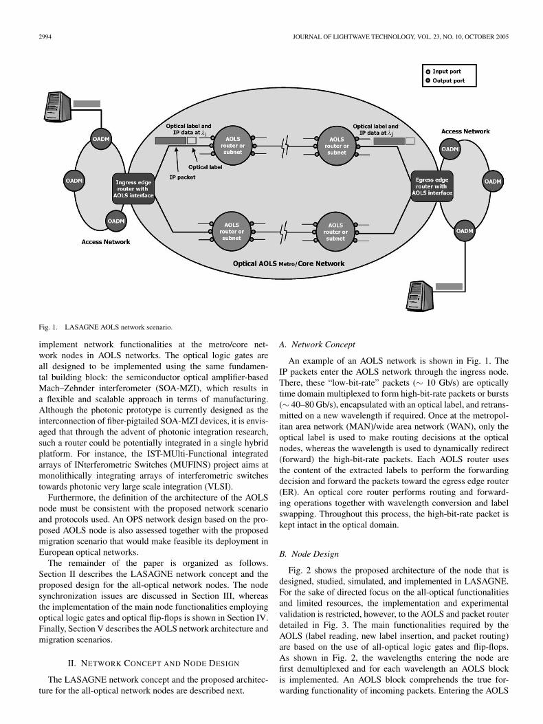
Fig. 1. LASAGNE AOLS network scenario.
implement network functionalities at the metro/core net-work nodes in AOLS networks. The optical logic gates areall designed to be implemented using the same fundamen-tal building block: the semiconductor optical amplifier-basedMach–Zehnder interferometer (SOA-MZI), which results ina flexible and scalable approach in terms of manufacturing.Although the photonic prototype is currently designed as theinterconnection of fiber-pigtailed SOA-MZI devices, it is envis-aged that through the advent of photonic integration research,such a router could be potentially integrated in a single hybridplatform. For instance, the IST-MUlti-Functional integratedarrays of INterferometric Switches (MUFINS) project aims atmonolithically integrating arrays of interferometric switchestowards photonic very large scale integration (VLSI).
Furthermore, the definition of the architecture of the AOLSnode must be consistent with the proposed network scenarioand protocols used. An OPS network design based on the pro-posed AOLS node is also assessed together with the proposedmigration scenario that would make feasible its deployment inEuropean optical networks.
The remainder of the paper is organized as follows.Section II describes the LASAGNE network concept and theproposed design for the all-optical network nodes. The nodesynchronization issues are discussed in Section III, whereasthe implementation of the main node functionalities employingoptical logic gates and optical flip-flops is shown in Section IV.Finally, Section V describes the AOLS network architecture andmigration scenarios.
II. NETWORK CONCEPT AND NODE DESIGN
The LASAGNE network concept and the proposed architec-ture for the all-optical network nodes are described next.
A. Network Concept
An example of an AOLS network is shown in Fig. 1. TheIP packets enter the AOLS network through the ingress node.There, these “low-bit-rate” packets (∼ 10 Gb/s) are opticallytime domain multiplexed to form high-bit-rate packets or bursts(∼ 40–80 Gb/s), encapsulated with an optical label, and retrans-mitted on a new wavelength if required. Once at the metropol-itan area network (MAN)/wide area network (WAN), only theoptical label is used to make routing decisions at the opticalnodes, whereas the wavelength is used to dynamically redirect(forward) the high-bit-rate packets. Each AOLS router usesthe content of the extracted labels to perform the forwardingdecision and forward the packets toward the egress edge router(ER). An optical core router performs routing and forward-ing operations together with wavelength conversion and labelswapping. Throughout this process, the high-bit-rate packet iskept intact in the optical domain.
B. Node Design
Fig. 2 shows the proposed architecture of the node that isdesigned, studied, simulated, and implemented in LASAGNE.For the sake of directed focus on the all-optical functionalitiesand limited resources, the implementation and experimentalvalidation is restricted, however, to the AOLS and packet routerdetailed in Fig. 3. The main functionalities required by theAOLS (label reading, new label insertion, and packet routing)are based on the use of all-optical logic gates and flip-flops.As shown in Fig. 2, the wavelengths entering the node arefirst demultiplexed and for each wavelength an AOLS blockis implemented. An AOLS block comprehends the true for-warding functionality of incoming packets. Entering the AOLS

RAMOS et al.: IST-LASAGNE: LABEL SWAPPING EMPLOYING OPTICAL LOGIC GATES AND FLIP-FLOPS 2995
Fig. 2. Proposed photonic routing architecture.
module, the packet payload (40 Gb/s) and label (10 Gb/s) areseparated [9], as shown in Fig. 3. The extracted optical label isfed to a bank of optical correlators based on all-optical logicXOR gates (AOLXGs) [10], where the comparison between thelabel and a set of local addresses is performed. These localaddresses are generated using optical delay lines (ODLs). AnODL is comprised of a set of interconnected fiber delay lines,couplers, and splitters that generate a bit sequence out of onepulse. Thus, comparing the incoming label to the local ad-dresses implies that for each possible incoming label a separateODL and a correlator have to be installed in the AOLS block.After comparison, a high intensity pulse will appear at theoutput of the XOR correlator with the matching address. Thispulse feeds a control block that drives a wavelength converter.The control block is made-up of all-optical flip-flops (AOFFs)[11]. Depending on the matching address (correlator outputpulse), the appropriate flip-flop will emit a continuous wave(CW) signal at a certain wavelength. In this way, the internalwavelength is chosen. Meanwhile, a new label is generatedin the appropriate ODL. The new label is inserted in frontof the payload and both the payload and the new label arenow converted to the wavelength generated by the flip-flop.The packet is then sent through an arrayed-waveguide grating(AWG); therefore, the wavelength on which the packet leavesthe AOLS block determines the outgoing port on which thepacket leaves the node. Two switches provide the flexibilityto configure the assignments between the incoming labelsand the outgoing labels and wavelengths. The size of the packet
router (for example, number of optical correlators and flip-flops) is very dependent on the number of local addressesused in the routing table. The AOLS subsystem of Fig. 3 wasdepicted for the specific case of four different locally generatedaddresses (2-bit optical labels).
The synchronization between the optical subsystems em-ployed in the AOLS routing node and the timing informationof the incoming packet is of crucial importance for the properoperation of the node. The AOLS node requires timing extrac-tion on a packet-by-packet basis and a packet arrival detec-tion scheme. These functionalities are performed by a clockrecovery circuit [12] and a single-pulse generator. The former isplaced at the beginning of the router and is capable of handlinghigh-bit-rate burst mode optical packets. The latter generatesan optical pulse as a packet arrives to the AOLS. Therefore, theswitches used for generating the reference addresses and thenew label are controlled by a low-speed dynamically controllednetwork control plane (CP).
C. AOLS Contention Resolution Design
In Fig. 2, optical packet contention can happen near theoutput fiber ports of the AOLS packet switch when there ismore than one optical packet trying to exit to one output fiberat the same time on the same wavelength or when there aremore than four optical packets trying to exit to one outputfiber at the same time. However, at the time of writing, thereis no known solution for a complete all-optical contention

2996 JOURNAL OF LIGHTWAVE TECHNOLOGY, VOL. 23, NO. 10, OCTOBER 2005
Fig. 3. Experimental verification of LASAGNE label swapper and packet router.
resolution block design for the output-buffered AOLS packetswitch, which requires all-optical packet contention detection,all-optical control for the variable optical delay, and all-opticalcontrol of the tunable wavelength conversion. Electronic con-trol is a requisite to realize the contention resolution for suchan AOLS packet switch. Therefore, all-optical input-bufferedcontention resolution for the AOLS packet switch is presentedin this section.
The layout of such a contention-free nonblocking AOLSpacket switch design is shown in Fig. 4. The main principleof the contention resolution schemes is deploying more in-ternal and external wavelengths in the AOLS systems andnetworks. In the example shown in Fig. 4, 16 wavelengthsare used instead of four in Fig. 2. These 16 wavelengths{λ1 − λ16} consist of four groups of four wavelengths thatthe 4 × 4 AWG will treat cyclically, which means that the4 × 4 AWG routes the four wavelengths in the group {λ1 −λ4}, {λ5 − λ8}, {λ9 − λ12}, and {λ13 − λ16}, respectively,the same way. This is referred to as the cyclic characteristicof an AWG [13]. Based on this characteristic, we configurethe second wavelengths of the optical flip-flops in Fig. 4 inan ordinal way from λ1 to λ16, four as a group as explainedearlier, so that the AWGs in Fig. 4 behave exactly the sameway as in Fig. 2. Consequently, in Fig. 4, the optical packetscoming out of the AWGs during the same period can have upto 16 different wavelengths, but there are never optical packetson the same wavelengths trying to exit to one output fiber at the
same time. For example, in an extreme case where contentionis most likely to happen, assuming at one time all the incomingoptical packets entering the switch are destined to the sameoutput fiber, in the AOLS packet switch in Fig. 4, these 16optical packets will be converted, respectively, onto λ1 − λ16,so that they can be sent out to that output fiber contention freewithout delay after the AWGs.
As a result, the AOLS network of the AOLS packet switchesin Fig. 4 employs 16-wavelength wavelength division mul-tiplexing (WDM) instead of the four-wavelength WDM inFig. 2. Therefore, at each input fiber, there are also possiblyup to 16 wavelengths instead of four. Since the AOLS packetswitch was originally designed for four-wavelength WDM andthus can only deal with four wavelength channels per fiber ata time, waveband demultiplexers are introduced here to sepa-rate the 16-channel WDM traffic into four groups of the fourwavelengths that every AOLS array (per AWG) can processat the same time. Synchronization is still necessary after thewaveband demultiplexers to keep the optical packets from thesame input fiber port aligned. Fixed optical delay units (∆t)are deployed to allow for the processing time of the opticalpackets in different wavelength groups. ∆t is determined by theAOLS processing duration for one optical packet, so its valueis fixed and can be estimated beforehand.
The following preconditions exist and are satisfied: 1) AWGshave cyclic characteristics [13]; 2) the AOLS does not processthe wavelength information of the incoming packets; 3) the

RAMOS et al.: IST-LASAGNE: LABEL SWAPPING EMPLOYING OPTICAL LOGIC GATES AND FLIP-FLOPS 2997
Fig. 4. Regular AOLS packet switch schematic configuration with contention resolution.
wavelength receiving and operation ranges of the AOLS arebeyond {λ1 − λ16}; 4) WDM allows us to use the enormousfiber bandwidth; 5) for high data processing rate, negligiblelatency is caused by the queuing in different wavebands.
The advantages of the scheme include the following:1) contention is completely solved; 2) it is at the moment,to our knowledge, the only all-optical contention resolutionfor this kind of AOLS packet switches; 3) apart from thewavelength resource, it technically does not add any moredifficulty or complexity on the AOLS packet switch buildup;4) the operation principle is simple and intelligible; 5) onlyinput packet synchronization is required. The disadvantagesinclude: 1) usage of more wavelength resource; 2) the queuingof the wavebands might introduce unnecessary delay; and 3)further investigation needs to be carried out concerning the all-optical synchronization of different wavebands.
III. ALL-OPTICAL NODE SELF-SYNCHRONIZATION
The LASAGNE AOLS scenario involves the design andimplementation of an all-optical node capable of receiving,processing, and routing packet traffic solely in the opticaldomain. Optical data processing, however, requires the pres-ence of an all-optical synchronization stage at the input ofthe node that will be used to control or power-up subsequentnode subsystems. Considering the defined AOLS scenario thatblends a packet-switched network with all-optical signalprocessing, such a synchronization stage should be capable ofoperating at the line rate and on a packet-by-packet basis while
maintaining high bandwidth utilization factors. The ability toperform with packets allows for bandwidth-on-demand use,whereas low overheads lead to effective processing of smallerpackets that eventually define the granularity of the network.In this rationale, aside from the technological performancemetrics, the most important attribute of such synchronizationcircuits is their capability to operate with packets, a fact thatrequires low lock-in time and low persistence time. In thisrationale, two synchronization modules are reported and theirproof-of-principle is experimentally verified: a packet clockrecovery operating at 40 Gb/s capable of extracting the clockon a per-packet basis and a packet-rate clock recovery at10 Gb/s capable of generating a single pulse per incomingpacket. These self-synchronization modules were specificallydesigned so as not to require local signal generation and/orsynchronization of incoming packets with local optical orelectrical oscillators.
A. 40 Gb/s Packet Clock Recovery Circuit
In this section, the principle of operation and the experimen-tal validation of the packet clock recovery circuit operating at40 Gb/s are reported. In contrast to previously reported opticalclock recovery circuits [14]–[16] comprising of high-Q cavities,the approach proposed here uses a low-Q passive filter in com-bination with a power-limiting optical gate to achieve instantlocking and low clock persistence time, as described in [12].Exploiting the memory effect of such a low-Q comb-generatingfilter, packet-to-packet processing is achievable due to the short

2998 JOURNAL OF LIGHTWAVE TECHNOLOGY, VOL. 23, NO. 10, OCTOBER 2005
Fig. 5. Packet clock recovery experimental setup.
impulse response of the filter. The bit wise processing offeredby optical gates is then used to produce high-quality recoveredclock packets, where a cascaded optical gate plays the role ofthe power limiter.
The block diagram of the experimental setup is shown inFig. 5 and consists of the optical packet generator and theclock recovery circuit. An actively mode-locked fiber ring laser(MD-FRL) provided a 9.872-GHz pulse train consisting of1.6-ps pulses at 1555 nm. This pulse train was modulated toform a 27 − 1 pseudo-random binary sequence (PRBS) signalusing a PRBS generator and a Ti:LiNbO3 modulator (MOD1)and was then rate upgraded in a fiber-based bit interleaverto generate 39.488 Gb/s pseudo-data stream. Data packetswere then generated using a second electrooptic modulator(MOD2) driven by a programmable PRBS generator. Thedata packets were fed into the packet clock recovery circuit,consisting of a low-Q Fabry–Pérot filter (FPF) and an SOA-based ultrafast nonlinear interferometric (UNI) gate, poweredby a CW signal at 1550 nm [laser diode 2 (LD2)]. The FPFplayed the role of the passive optical resonator that extractsthe line rate spectral component. Exploiting the filter memoryeffect, the data packets are transformed into clock packetswith intense amplitude modulation. The FPF used was a bulkmicrometer-adjustable fused quartz substrate with free spectralrange (FSR) equal to the line rate and finesse equal to 50. Theoutput of the filter was amplified and inserted into the UNIgate as the control signal. The UNI gate was optimized for40 Gb/s operation by using a polarization-maintaining (PM)fiber that induces 5 ps of birefringent delay in the two orthog-onal polarization components of the input and output ports ofthe gate. As a result, an asymmetric switching window withrespect to the bit slot is formed, relaxing the requirement forthe SOA recovery time. The saturation of the gate by CWlight injection close to the SOA material transparency resultsin a strongly nonlinear step-like transfer function [17]. Thisprovides the intensity modulation reduction that is necessaryfor generating a packet-level clock signal from the amplitude-modulated Fabry–Pérot output. Finally, the self-extracted clockpackets were amplified in an erbium-doped fiber amplifier(EDFA) and launched into a dispersion-decreasing fiber (DDF)-based pulse compressor used at the output of the UNI gate. Theactive element of the UNI gate was a 1.5-mm bulk InGaAsP/InPridge waveguide SOA provided by OPTOSPEED S.A. with27 dB of small signal gain at 1550 nm and a recovery time of80 ps when driven with 700 mA.
Fig. 6 shows a sequence of four 40-bit-long packets separatedby 750 ps at 40 Gb/s. The FPF partially fills the zeros withinthe packet due to its low finesse so that deeply amplitude-modulated but clock-resembling packets are obtained as shownin Fig. 6(b). When this signal is fed as control into the sat-urated UNI gate, clock packets with very short rise and falltimes are generated and depicted in Fig. 6(c). Fig. 6(d)–(f)provides a more detailed view of a single packet, its form afterpassing through the FPF and its transformation to an amplitude-equalized packet clock signal at the output of the gate. Fig. 6(f)shows that the clock is captured from the first bit and exhibitsa fall time of 16 bits, whereas the amplitude modulation (high-est to lowest pulse ratio) within the 40 clock pulses is below1 dB. The sharp rise time is a result of the heavy saturation ofthe SOA and determines the lock acquisition time of the circuit,whereas the fall time is due to the lifetime of the filter anddetermines the minimum intrapacket guardbands. The circuitwas operated by injecting 1 mW of optical power from the CWsignal and 80 fJ pulse from the data signal.
The timing jitter performance of the circuit was measuredusing a continuous PRBS signal at 40 Gb/s with the precisiontime base option of an Agilent/HP 86100A Infinium digitalsampling oscilloscope. Fig. 7(a) shows the eye diagram ob-tained for the input signal at 40 Gb/s with a root mean square(rms) timing jitter of 450 fs. The reshaping properties of thepower-limiting gate are shown in Fig. 7(b) through the eye dia-gram of the recovered clock at 40 GHz with a measured timingjitter of 580 fs. The slight increase in rms jitter was due to thedifficulty of precisely aligning the bulk FPF used, resulting insmall line rate detuning. This effect can be eliminated by usingfiber-based FPFs.
Using two preamble bits, the clock is captured from the firstbit (instantaneous locking) and persists for the duration of thedata packet increase by an exponential decaying tail of only16 bits. Although the experimental data presented use a 27 − 1PRBS, the clock recovery circuit can be designed according tothe requirements of the network traffic by tailoring the finesseof the FPF. For instance, if a PRBS of 231 − 1 is required, thefilter should be designed to have a finesse of 80 [12]. In thiscase, the recovered clock packet would exhibit less than 150 pslock-in time and a decay time of approximately 2 ns. Also, sinceFPF has over 50 nm of optical bandwidth, the clock recoverycircuit is only limited by the gain bandwidth of the SOA used,making the scheme broadband and insensitive to laser sourcewavelength instabilities.

RAMOS et al.: IST-LASAGNE: LABEL SWAPPING EMPLOYING OPTICAL LOGIC GATES AND FLIP-FLOPS 2999
Fig. 6. (a), (b), and (c) input data packets, FPF output, and recovered clock packets at 500 ps/division time base. (d), (e), and (f) single packet, FPF output, andrecovered clock at 200 ps/division time base.
Fig. 7. Eye diagrams of (a) input data packets and (b) recovered clock packets. The time base is 10 ps/division.
B. Packet-Rate Clock Recovery Circuit
This subsection is concerned with the design and experimen-tal validation of the packet-rate clock recovery circuit that isnecessary for powering and controlling the LASAGNE opticalgates as described in Section II. The circuit is responsiblefor generating a single pulse per incoming packet analogousto the frame synchronization pulse in traditional synchronousoptical network (SONET)/synchronous digital hierarchy (SDH)systems. Specifically, for the design of LASAGNE node, the
packet-rate clock recovery circuit is interconnected with thelocal address generation and the optical correlator blocks, asshown in Fig. 3.
Previous implementations of single-pulse extraction tech-niques involve a marker pulse at the beginning of the packetat a different state relative to the rest of the packet in termsof either wavelength [18], polarization [19], bit period [20],or amplitude [21], resulting in increased complexity to thegeneration and transmission of packets. More recently, exper-iments have been reported where all the pulses of the packet

3000 JOURNAL OF LIGHTWAVE TECHNOLOGY, VOL. 23, NO. 10, OCTOBER 2005
Fig. 8. Experimental setup of packet-rate clock recovery at 10 Gb/s.
share the same physical state [22], [23]. In these approaches, anSOA with a very long recovery time is required [22], which inturn introduces very long guard bands between the transmittedpackets or specific coding techniques [23]. The packet-rateclock recovery proposed here only requires the clock recoverycircuit described in the previous section and a single SOA toextract a single pulse from each incoming data packet withoutadditional signaling or guard-band requirements.
The block diagram of the experimental setup is depicted inFig. 8 and consists of the data packet generator, the packet clockrecovery circuit, and an additional SOA device. To generatethe data packets, a distributed feedback (DFB) LD1 emittingat 1549 nm was gain switched at 2.5815 GHz, providing10-ps full-width at half-maximum (FWHM) pulses after linearcompression. This pulse train was modulated with a 27 − 1PRBS in a Ti:LiNbO3 modulator (MOD1) and was inserted ina fiber-based bit interleaver to generate a pseudo-data pattern at10.326 Gb/s. A second Ti:LiNbO3 modulator (MOD2), drivenby a programmable pulse generator, modulated this PRBSdata stream into packets of 4-ns length at 80.672 MHz, whichthen entered the clock recovery circuit. In accordance with theprevious section, a clock packet is self-extracted from eachcorresponding data packet entering the clock recovery circuit.After amplification through an EDFA, the extracted clockpackets were split and inserted into a 1.5-mm SOA in a counter-propagating fashion, synchronized with 1-bit offset. The oper-ation of the circuit relies on cross-gain modulation (XGM) andthe specific temporal synchronization of the involved signalswithin the amplifier. Due to the single-bit delay induced, onlythe first clock pulse experiences amplification, whereas subse-quent probe pulses are suppressed through the interaction withthe counter-propagating strong pump signal incident on theSOA. Fine synchronization of the signals was achieved usingODL1 and both signal polarization states needed adjustmentsdue to the polarization dependence of the SOA used.
Fig. 9 shows typical oscilloscope traces verifying the circuitprinciple of operation. More specific, Fig. 9(a) and (d) shows
the 4-ns optical packets separated by 8.4 ns and Fig. 9(b) and(e) shows the recovered clock packets exhibiting a 2-bit risetime and an 8-bit fall time. This signal is then split and insertedinto the SOA responsible for the single-pulse extraction. Therecovered clock packet acting as the probe signal is within thesmall-signal-gain region of the amplifier, and the first preamblepulse enters the SOA that is fully unsaturated. After experienc-ing full amplification, it exits the SOA. The remaining clockpulses are suppressed through gain saturation induced by thecounter-propagating strong recovered clock signal, acting asthe pump. As a result, a single pulse is allowed to exit theSOA, and this is shown in the oscilloscope traces of Fig. 9(c)and (f). The switching power/energies used in the UNI gatewere 0.8 mW for the CW power and 110 fJ for the controlinput. The single-pulse extraction required 300 and 15 fJ forthe pump and probe signals, respectively, in order to invokeXGM within the amplifier. Since the circuit relies on saturationeffects within an SOA, the operational speed of the circuit isdictated only by the packet clock recovery circuit, making thescheme upgradeable to 40 Gb/s. The proposed circuit will beexperimentally verified using 40 Gb/s packets combined withan SOA-MZI-based packet clock recovery during the secondphase of the project.
IV. NODE FUNCTIONALITIES EMPLOYING ALL-OPTICAL
LOGIC GATES AND OPTICAL FLIP-FLOPS
All-optical logic gates and optical flip-flops are considered asthe basic functional block for implementing the key function-alities required at the optical node: label and payload separa-tion, label reading, tunable wavelength conversion, and packetrouting. Detailed structure and performance results for thesesubsystems are provided in this section.
A. Label/Payload Separation Circuit
The optical circuit responsible for separating the label fromthe payload [9] of incoming data packets is presented in this

RAMOS et al.: IST-LASAGNE: LABEL SWAPPING EMPLOYING OPTICAL LOGIC GATES AND FLIP-FLOPS 3001
Fig. 9. (a) and (d): Input data packets; (b) and (c): Generated clock packets; (c) and (f): Output pulses at packet rate. Time base in (a), (b), and (c) is200 ps/division and in (d), (e), and (f) 400 ps/division.
subsection and the principle of operation is verified throughsimulation studies using the commercially available simulationtool VPI TransmissionMaker at 40 Gb/s. Fig. 10(a) showsa schematic diagram of the label/payload separation circuitalong with its principle of operation. The circuit consists oftwo subunits: the previously described optical packet clockrecovery circuit and an additional high-speed optical gate,both simulated here as SOA-MZI gates operable at 40 Gb/s.The incoming data packets are split into two parts, one usedas input in the clock recovery circuit (MZI1) and one to enteras data signal in MZI2. The extracted optical packet clocksignal persists for the duration of the original data packet andis used as the control signal in MZI2. For label separation,MZI2 is configured to perform a simple Boolean AND operationbetween the original incoming packet stream and a delayedversion of the recovered packet clock after optical filtering.Successful label/payload separation is obtained if the originalpacket and the extracted clock are temporally delayed by anamount equal to the packet label length increased by the risetime required for clock acquisition. As such, the packet clockis delayed in an ODL so that only the payload bits of the orig-inal packet fall within the switching window of the recoveredclock and are therefore switched at the gate output. Fig. 10(b)shows the packet format chosen for the experimental vali-dation of the LASAGNE node consisting of the optical headerand payload sections. The optical header contains two pream-ble and one stuffed bit to assist the clock extraction process
and two label bits separated by 100 ps. The specific formatwas chosen to guarantee successful clock recovery and to relaxthe SOA recovery time requirements in the all-optical XOR
correlators described in the next subsection. The payload of thedata packet was a 27 − 1 PRBS with 1.5-ns duration.
Fig. 11 shows typical simulation results of the 40 Gb/slabel/payload separation circuit obtained using the commercialsimulation tool. Fig. 11(a) shows the incoming data packethaving an optical header “11010100” with an embedded opticallabel “01.” Fig. 11(b) shows the recovered packet clock withinstantaneous locking and 12 bits 1/e fall time. Fig. 11(c)and (d) shows the extracted label and payload, respectively,whereas the insets depict eye diagrams of four packets con-taining all possible 2-bit label combinations. Analysis of thesimulation results reveals an extinction ratio of 13 dB for theextracted label and 11 dB for the extracted payload, whereasboth pulse traces have less than 0.7 dB of pulse-to-pulse ampli-tude modulation.
B. All-Optical Correlators Based on Logic XOR Gates
In order to take the packet routing decisions inside theLASAGNE node, the labels of the incoming packets need to becompared with specific address keywords. One common wayto perform this optical bit pattern recognition is through theuse of a time-domain optical correlator to match a series ofbits to an optical look-up table. The way to implement this

3002 JOURNAL OF LIGHTWAVE TECHNOLOGY, VOL. 23, NO. 10, OCTOBER 2005
Fig. 10. Schematic diagram showing (a) principle of operation of label/payload separation circuit using two SOA-MZI gates and (b) optical packet format.
Fig. 11. Simulation results of label/payload separation circuit at 40 Gb/s showing pulse traces of (a) incoming data, (b) recovered packet clock, (c) extractedlabel, and (d) extracted payload with insets showing eye diagrams of four packets containing all possible 2-bit label combinations. Time base is 200 ps/division.

RAMOS et al.: IST-LASAGNE: LABEL SWAPPING EMPLOYING OPTICAL LOGIC GATES AND FLIP-FLOPS 3003
Fig. 12. Proposed architecture for the all-optical label processor or optical correlator.
functionality in LASAGNE is by means of AOLXG basedon SOA-MZI devices. However, the implementation of thissubsystem is limited to four correlators (e.g., four output portsor wavelengths in the node), which gives rise to 2-bit opticallabels (Fig. 3).
The proposed architecture for the all-optical label pro-cessor (optical correlator) is shown in Fig. 12 [24]. It ismainly based on a cascade of photonic-integrated SOA-MZIs.Each one of these SOA-MZIs is configured to operate as alogic XOR gate as in [25], but using a counter-propagatingscheme to avoid optical filtering between different stages.The two input data streams are coupled into ports 1 and 2of the MZI, while a CW light is coupled into port 3. Theoutput signal at port 4 of the first SOA-MZI is the resultof a logic XOR operation of both data streams. This outputsignal, after proper optical attenuation and delay, is launchedinto port 3 of the second SOA-MZI synchronized with thesecond bit of the data patterns. The main difference betweenthe first stage and the second and further stages is that theinput signal at port 3 is not a CW signal, but a pulsed one,which acts as an enabling signal as in [10]. Although it isnot directly shown in the schematic diagram of Fig. 12, theoptical lengths of the waveguides transporting both data sig-nals need to be carefully adjusted to assure that each bit ofthe data patterns is perfectly synchronized between them andthe control signal. By cascading the different SOA-MZI struc-tures, we obtain the logic function
S(j)i = S
(j−1)i−1 Ci (1)
where S(j)i is the ith bit of the signal at the output of the jth
stage and Ci is given by
Ci = Ai ⊕ Bi (2)
where Ai and Bi are the ith bits of the input data signals tothe optical correlator. S
(0)i = 1 represents the CW input signal
to stage 1. By considering that the bit length of the data inputsand the number of stages is equal to N , the output of the wholedevice would be
S(N)i = 0, i < N ; S
(N)N =
{0, if A �= B1, if A = B.
(3)
Therefore, the device can be employed as an all-optical corre-lator for bit-pattern matching applications by introducing theone’s complement of one of both data signals or addresses tobe compared.
Fig. 13. Simulation results of bit-pattern matching (label/addressrecognition).
In order to validate by simulation the architecture operation,the Virtual Photonics Inc. software was used. A transmissionline laser model technique has been applied to model theSOAs [26]. The SOAs in the MZIs are characterized by a lengthof 500 µm, a linewidth enhancement factor of 8.0, a confine-ment factor of 0.3, a carrier lifetime of 16.3 ns, a spontaneousemission factor of 1.5, and a drive current of 250 mA. The simu-lation results are shown in Fig. 13 for 4-bit words. Two 10 Gb/s

3004 JOURNAL OF LIGHTWAVE TECHNOLOGY, VOL. 23, NO. 10, OCTOBER 2005
Fig. 14. Arrangement of two coupled identical lasing cavities showing the possible states. In State 1, light from Laser 1 suppresses lasing in Laser 2. In State 2,light from Laser 2 suppresses lasing in Laser 1. To change states, lasing in the master is stopped by injecting light not at the lasing wavelength.
data inputs [30-ps FWHM return to zero (RZ) Gaussian pulsesat 1553.6 nm] comprised of several bit patterns were appliedto the correlator: A = [1000, 0011, 1110, 0100, 1011] and B =[0011, 1101, 1001, 1011, 0010]. Only the fourth word in datainput B is exactly the one’s complement of the fourth word indata input A. Therefore, only an address matching signal is ex-pected for this word at the output of the whole architecture. Theoutput signals from each SOA-MZI stage are shown in Fig. 13,where it can be seen that only an optical pulse is obtained atthe output of the device (fourth stage output) for the fourth dataword that validates its header/address recognition functionality.The extinction ratio of the output signal was found to be higherthan 15 dB.
Although the architecture has been simulated at 10 Gb/s,this can be extended to 40 Gb/s optical labels by employinga differential scheme at the SOA-MZI inputs [27].
C. Optical Flip-Flops
The AOFF memory that we use is based on two coupledlasers with separate laser cavities. A schematic of the flip-flop isdepicted in Fig. 14. The system can have two states. In State 1,light from Laser 1 suppresses lasing in Laser 2. In this state,the optical flip-flop memory emits CW light at wavelength λ1.Conversely, in State 2, light from Laser 2 suppresses lasing inLaser 1. In state 2, the optical flip-flop memory emits CW lightat wavelength λ2. To change states, lasing in the dominant lasercan be stopped by injecting an external light at the dominantlaser’s lasing wavelength. A critical issue is the amount ofcoupling between the two lasers. The minimum amount ofcoupling between the lasers that is required to obtain bistableoperation depends on the implementation, but the couplingshould be strong (typically 40% or larger) [28].
An asymmetrically biased system of two coupled lasers (bysetting the bias current differently for Laser 1 as for Laser 2)can also form an all-optical threshold function. As a result ofthis, Laser 1 injects a different amount of light into Laser 2than the amount of light that Laser 2 injects into Laser 1. Weassume that the amount of light that Laser 1 injects into Laser 2is sufficient to suppress lasing of Laser 2. Hence, Laser 1 is thedominant laser. On the other hand, we assume that the amount
Fig. 15. Ring laser implementation of the optical flip-flop memory. SOA:semiconductor optical amplifier, ISO: isolator, FPF: Fabry–Pérot filter.
of light that Laser 2 injects into Laser 1 is not sufficient tosuppress lasing of Laser 1. If an additional amount of externallight is injected into Laser 1, so that the combined powerinjected into Laser 1 exceeds the power required to suppresslasing, Laser 1 can be temporarily switched off. Hence, Laser 2becomes the dominant laser as long as the external light isinjected into Laser 1. As soon as injection of external lightstops, the system switches back and hence Laser 1 becomes thedominant laser again. The system of two coupled lasers is nowan optical threshold function (OTF) instead of an optical flip-flop memory.
Fig. 15 shows the experimental set-up for an experimentto demonstrate the operation of the optical flip-flop memory.The two SOAs act as the lasers’ gain media. In this particularset-up, a ring laser configuration is used. We have used FPFswith a bandwidth of 0.18 nm as wavelength selective elements.SOA 1 was pumped with 168 mA of current and SOA 2 waspumped with 190 mA of current. The pulses that were used toset and reset the flip-flop had a power of 2 mW. The opticalspectrum of the flip-flops’ output states is presented in Fig. 16.It is clearly visible that the difference in output power betweenthe two states is over 45 dB. The switching characteristics ofthe optical flip-flop are presented in Fig. 17. It can be observedfrom Fig. 17 that if a sufficient external pulse is coupled in theflip-flop, the system changes states.
It should be noted that it is also possible to realize optical flip-flops by coupling other optical nonlinear elements than lasers.Examples are given in [29]–[31], in which flip-flop operation

RAMOS et al.: IST-LASAGNE: LABEL SWAPPING EMPLOYING OPTICAL LOGIC GATES AND FLIP-FLOPS 3005
Fig. 16. Spectral output of two states of the optical flip-flop memory ispresented. The solid curve represents the state in which laser 1 is lasing, andthe dotted curve represents the state in which laser 2 is lasing.
is demonstrated by using coupled nonlinear Mach–Zehnderinterferometers and coupled nonlinear polarization switches.
Photonic integration of optical flip-flops is essential forapplications in optical networks. Integrated optical flip-flopmemories should have fast (optical) set and reset times, operateat low power, have a high contrast ratio, and should havesufficiently small dimensions. An integrated optical flip-flopmemory based on laser operation is presented in [32], but thepower consumption, the size, and the switching speed of thesedevices remain an issue, which makes it difficult to couple themin large quantities as required in optical shift registers. A morepromising AOFF concept based on two coupled microlasers ispresented in [33]. This flip-flop concept has the potential tohave the dimensions in the order of the wavelength of light, aswitching speed of a picosecond, and a switching energy belowa femtojoule. If one succeeds to interconnect these flip-flops,densely integrated digital optical logic operating at high speedand low power can be realized.
D. Tunable Wavelength Conversion and Packet Routing
In the LASAGNE node, a tunable wavelength converter re-ceives the incoming optical packets and converts them onto thenew wavelength channel set by the optical flip-flop blocks. Withan AWG wavelength demultiplexer, routing of the optical pack-ets can be further implemented. General system requirementson the optical wavelength converters include polarization in-sensitivity, broadband operating wavelength range, etc. Morespecifically, in LASAGNE node, two challenges are presentfor the SOA-MZI wavelength converters. First, the SOA-MZIis required have a large modulation bandwidth to perform thewavelength conversion of the RZ signals at 40 Gb/s or higher bitrate. Second, fast wavelength tunability requires the wavelengthconverter to have a tunable-filter-free configuration. In the node,the wavelength of the probe light is changing fast within severalnanoseconds. A tunable filter cannot be optically controlled andtuned at such a high speed.
To fulfill the above system requirements, SOAs with fastgain recovery time are required and the configuration schemeof SOA-MZI also needs to be optimized. Generally, a singleSOA-MZI can be dual-arm driven or single-arm driven bythe modulating signals; it can also be configured to operatewith either co-propagating or counter-propagating probe andmodulating signals. The combinations of these operating modesresult in various configuration schemes.
The differential driving scheme with co-propagating signalshas the best modulation performance. Fig. 18 shows the cal-
Fig. 17. Oscilloscope traces showing power of laser 1 and laser 2. Regulartoggling between the states can be clearly observed.
culated eye-opening penalty of a converted 40 Gb/s RZ signalin single-arm-driven and differential-driven modes. With thegain recovery time increasing beyond 30 ps, the SOA-MZI inthe standard mode outputs nonreturn to zero (NRZ)-like eyediagrams and exhibits severe intersymbol interference (ISI).On the other hand, the eye opening of the output signal isgenerally acceptable as long as the gain recovery time is limitedbelow 100 ps. Compared to the single-arm-driven mode, thedifferential mode greatly relaxes the requirements on the SOA’sgain recovery time. However, the co-propagating configura-tion requires special waveguide design to realize the filter-freeconfiguration [34].
The counter-propagation scheme is simpler to implement.More importantly, it is a filter-free configuration. However,the switching performance of the SOA-MZI is very sensitiveto the SOA chip length in this scheme, and severe ISIs maybe observed for high SOA lengths. Therefore, such a schemerequires the use of short chip length SOAs. Compared with theco-propagating case, this scheme has the same requirement onthe SOA gain recovery time and has further requirements onthe chip length, implying more challenges to fabrications of fastgain response SOA chips.
Another scheme is to construct the wavelength convertermodule using two cascaded SOA-MZIs, as shown in Fig. 19.This scheme features a tunable-filter-free configuration. Theincoming 40 Gb/s pulses modulate the first SOA-MZI stage,transferring the incoming data onto the wavelength set by aninternal CW laser. Then, the wavelength-converted signal isinjected into the second SOA-MZI as the modulating signal.The second SOA-MZI also receives the CW signal generatedby the optical flip-flops and transfers the modulating data ontoit. At the output, a notch filter is used to filter out the light gen-erated by the internal laser. In this way, the incoming 40 Gb/spulses are finally converted onto the wavelength set by theoptical flip-flop. Through using the filters with fixed centerwavelength, this module is able to achieve fast tunable wave-length conversion. Due to the cascading configuration, the maindisadvantage of this scheme is that the modulation bandwidthof the wavelength module is further degraded compared to thatconsisting of single SOA-MZI.
Each configuration has its own advantages and constraintsconcerning the network performance and functionalities. Theabove schemes of the SOA-MZI will be experimentally investi-gated with respect to its wavelength conversion performance inthe LASAGNE network node.

3006 JOURNAL OF LIGHTWAVE TECHNOLOGY, VOL. 23, NO. 10, OCTOBER 2005
Fig. 18. (a) SOA 10%–90% gain recovery time versus eye-opening penalty. (b) Eye diagrams of a 40 Gb/s RZ signal.
Fig. 19. Wavelength converter consisting of two cascaded SOA-MZIs. The two SOA-MZIs operate in the differential mode to achieve the optimum switchingperformance. The scheme features by a tunable-filter-free configuration.
V. LASAGNE AOLS NETWORK
A. The Network Architecture
The AOLS solution proposed in LASAGNE is compatiblewith a number of different optical packet switching networkarchitectures. In other words, the node design described inprevious sections does not impose critical constraints to thenetwork design. So the results of networking studies have atwofold impact: on one side they depict a “preferred embodi-ment” of the LASAGNE network; on the other side they maygive a general contribution to the OPS research community.
The LASAGNE network is proposed as a single multiserviceconvergence technology in the core section of a European
operator network. The preferred architecture is a connection-oriented solution with label swapping performed at every node.The basic forwarding entity is a virtual connection, named OPSlabel switched path (LSP), that is an optical analogy of anMPLS LSP or an asynchronous transfer mode (ATM) virtualcircuit (VC). The basic data plane functionalities are labelprocessing, label swapping, and packet routing. The opticalheader contains a label field used for forwarding purposes. Apriority field has also been considered in order to accommodatecontention resolution techniques that manage different prioritylevels. The use of optical label swapping in an all-optical packetswitching network creates some challenges and opportunitiesfrom the networking point of view. On one hand, to lower the

RAMOS et al.: IST-LASAGNE: LABEL SWAPPING EMPLOYING OPTICAL LOGIC GATES AND FLIP-FLOPS 3007
Fig. 20. Label stripping strategy.
cost of the AOLS node, it may be beneficial to reduce thenumber of different labels used throughout the network andhence the number of bits occupied by the label. Together with areduction of the number of labels (or components), the projectalso targets to reduce the label length and thus the complexityof individual components. On the other hand, whereas anelectronically implemented look-up table was easy to adapt tochanging routing demands (i.e., LSPs are set up, broken downat all possible moments in the network), the number of all-optical components and how they are designed will be directlyrelated to the dimensions of the routers (and thus the abilityto accept more or fewer LSPs). Thus, the use of an all-opticalpacket switching poses restraints on the flexibility in routingand labeling the packets that should be well dimensioned. Tothis end, different label switching strategies are compared. Thefirst label switching strategy proposed is based on the MPLSrouting scheme. In an AOLS block, decisions are taken basedon an incoming label and the incoming port. These are swappedinto an outgoing label and an outgoing port. In the second labelswitching strategy (Fig. 20), a packet is switched through thenetwork based on an end-to-end label. This label consists ofmultiple local labels. In each intermediate node, the AOLSblock strips off the first bits of the end-to-end label (this isthe local label) and makes a switching decision (i.e., to whichoutput port the packet will be forwarded).
Both switching strategies are compared from a node dimen-sioning point of view. The dimension indicators that largelydefine the physical dimensions and implementation difficultyof the node are the following: 1) number of correlators: thenumber of correlators needed to distinguish the different pos-sible incoming labels, counted per incoming port; 2) length ofincoming ODL: the total number of ODLs needed to providethe local addresses multiplied by the delay line length of 1 bitand the number of bits in the incoming label. The node archi-tecture requires for each possible incoming label a correlatorand an incoming ODL. It is obvious that the more bits in a labeland the more different labels a node has to distinguish, the more(and longer) ODLs and correlators have to be implemented.This makes the label stripping strategy less demanding onresources than label swapping because for label stripping thepossible incoming labels are restricted to the number of outgo-ing ports in the node. This is confirmed by the dimensioningstudy, as can be seen from Fig. 21. Also, since the length of thelabels can be shorter (fewer number of bits), the length of theincoming ODLs is much smaller, greatly reducing the amountof ODLs installed in the node. In Fig. 21, the results fromthe dimensioning study are depicted as a proportion of both
switching strategies. We see clearly that label stripping needsfewer resources than label swapping. Although label swappingseems to be inferior to label stripping from a dimensioningpoint of view, we should take into account that the end-to-end label of label stripping induces much more overheadthan the label swapping label [e.g., end-to-end label for labelstripping = 3 bits(local label) × 8 hops = 32 bits, instead of an8-bit label for label swapping].
What has been described up to now is the “core part” ofthe OPS architecture. In order to accommodate client signals,a number of operations must be performed at the edge of anOPS network. We refer to these edge functionalities as “adap-tation layer.” The basic operation at the ingress/egress side isthe insertion/extraction of client information in/from opticalpackets that implies the definition of a mapping procedure:client protocol data units (PDUs) are inserted on the payloadof the optical packet together with some mapping informationthat allows the receiving node to extract the correct clientPDUs. We refer to this kind of information as “edge header”or, because the insertion/extraction is supposed to be performedelectronically, “electronic header.”
Another important function that should be defined at theedge of the network when designing the interworking betweenclient protocols and OPS is the translation of addressing in-formation of client signals into addressing information of OPSnetwork. The last consists of the LSP and the related label. So,basically, the said translation procedure is a table containingthe relationship between data flow of incoming client signalsand OPS LSP.
Two alternatives exist to implement edge functionality. Thefirst one consists of the design of an edge node (see Fig. 1)that would basically be a core node with some client cardadded. This card is supposed to be an electronic card, and map-ping, stuffing, and edge header generation are supposed to berealized there. Their outputs are OPS packets that are sent tothe “core portion” of the node. Dense WDM (DWDM) inter-faces in the edge node are used to connect it to core devices orto other edge devices. Interworking with client signals may bebased on one of the two approaches depicted in Fig. 22, withreference to IP clients.
1) Port-based mapping: All traffic incoming from a clientport is sent to the same OPS LSP. Note that this meansthat every IP router must have a dedicated connection tothe OPS node for every other IP router that it is connectedto. So the major drawback is that this approach is notoptimal in terms of number of client interfaces.
2) Client logic in the OPS node: In this case, the OPS nodehas the capability of reading IP addresses of incomingpackets and selecting different LSPs depending on them.The edge node becomes more complicated (please notethat the same intelligence would be necessary for allclient types) but this allows to reduce the number ofrouter–OPS connections.
The second alternative is the definition of OPS interfacesin client equipment (Fig. 23). The feasibility of this approachwould be constrained to the willingness of client equipmentvendor to modify their devices, and it would strongly depend

3008 JOURNAL OF LIGHTWAVE TECHNOLOGY, VOL. 23, NO. 10, OCTOBER 2005
Fig. 21. Label swapping versus label stripping.
Fig. 22. OPS/client interworking with ERs. (a) Port-based mapping and(b) address-based mapping with client protocols logic in the edge device.ER: edge router, CR: core router.
on the success of the OPS technology and on its advance instandardization. From a technical point of view, the solutionwould have the following consequences.
1) OPS nodes would not care about mapping upper layerprotocol addressing OPS virtual connections (OPS LSP).
2) The OPS node could definitely be an all-optical device,without the need of expensive electric client line cards.
3) Interaction between client and OPS devices would berequired in terms of signaling for an OPS LSP setup.
4) Client/OPS interworking would be simplified, becauseclient nodes would be able to forward packets on differentLSPs depending on the IP addresses.
The establishment and the maintaining of OPS LSP requirecontrol intelligence in every node. This leads to the definitionof an OPS CP. Through signaling protocols, CP instances ofinvolved nodes communicate in order to manage the LSPs.
Fig. 23. Alternative approach: OPS interfaces in client equipment that imple-ment adaptation layer functionalities.
Basic functionalities that would be needed are discovery, inorder to allow every node to know its neighbors; routing, inorder to make one node capable to choose the most convenientpath for LSPs; and signaling for label distribution, in order toexchange information related to which label to use for a givenLSP and to manage LSPs. Due to the high similarity betweenMPLS and OPS networks, approaches used in the MPLS worldcan be reused. In order to allow CP instances to communicate,an out-of-band approach, where CP messages use an indepen-dent network infrastructure, is preferred in an OPS frameworkdue to the low bandwidth requirements of CP connections andto the drawback of the alternative in-band solution that wouldimply electrooptic conversion of OPS control packet.
In a more general network vision, it is straightforward topropose the integration of the OPS CP within the generalizedmultiprotocol label switching (GMPLS) framework [35], whichwould consist of the definition of a new switching capability[optical packet switching (OPSC)].
B. Migration Scenarios
In this section, we will discuss the benefits of using all-optical packet switching in mixed packet/circuit network ar-chitectures. In the following, three approaches are described.The former is a transitional stage, the latter two form a so-lution to combine the benefits of both packet switching andcircuit switching.
The first examined migration scenario is the one depicted inFig. 24. Even if the OPS network is supposed to carry everytype of client traffic, the connection of client equipment to OPS

RAMOS et al.: IST-LASAGNE: LABEL SWAPPING EMPLOYING OPTICAL LOGIC GATES AND FLIP-FLOPS 3009
Fig. 24. Example of a migration scenario where some clients have migrated in the OPS network while others are still connected through a circuit network.
Fig. 25. Example wavelength-switched network to demonstrate the ORIONfunctionality. Capital letters denote IP/MPLS routers, while small letters denotethe OXCs. Packet flow is indicated by the numbers in the packets.
ERs would need a certain amount of time and the definition ofa migration policy while migrating from a truly circuit switchednetwork to a purely OPS network. In this transient, there wouldbe some clients that would already use the OPS network whilesome others would still be connected through a circuit-basedbackbone. For example, in Fig. 24, a migration scenario isdepicted, where ATM and IP client equipment are connectedthrough the OPS network (ER, CR) while SDH and gigabitEthernet client equipment are connected through an opticalcross-connect (OXC)-based network.
The second mixed scenario is somewhat the same as theprevious one. A separate OPS and wavelength-switched net-work uses separate wavelengths, but on the same physicalnetwork infrastructure. The basic idea is that traffic gets sentover the wavelength-switched network if capacity is available.If there is a shortage on the wavelength-switched network, thesurplus traffic gets sent over the OPS network. This wouldallow the wavelength-switched network to carry at least verystatic traffic, while if there are variations and burstiness theOPS network can handle it. Meanwhile, it would lower thesize requirements of the OPS nodes, but still improve efficiencya great deal.
Based on the previous scenario, a hybrid approach calledORION is proposed as the third migration scenario. Basically,
this takes the previous one step further, allowing the (O)PSnetwork and the wavelength-switched network to share re-sources at wavelength level. We will explain the core featuresof the ORION network concept (for a more detailed descriptionof the design, we refer to [36]). The basic idea in ORION is tostart from a wavelength-switched WDM network, where somewavelength paths are established. In a normal wavelength-switched network, a lightpath passes some node transparently,i.e., the node cannot access the data in the passing wavelength.In the example of Fig. 25, node D has no access to the IPpackets traveling in wavelength λ1. Only wavelengths startingor terminating in that node can be accessed. Suppose we havethe connections A-a-b-c-d-D on λ2, B-b-c-d-e-E on λ3, andA-a-b-c-d-e-E on λ1, established as indicated in Fig. 25. Thebasic problem with wavelength switching occurs in the follow-ing scenario: when the capacity of the lightpath AD is fullyused, and there is some temporary overload for this connection,the wavelength λ1 cannot be used to carry some of its traffic,as it is dedicated for connection AE. It is, however, perfectlypossible that the lightpath AE (on λ1) is only carrying a lowtraffic load, so that in fact at some moments in time it is empty(assuming IP directly over WDM). Thus, while connectionAD has a capacity shortage, AE has capacity in abundance.While ordinary wavelength-switched WDM networks cannotsolve this type of situation instantly, ORION enables the net-work to use this capacity on λ1 (normally dedicated to theconnection AE) for the connection AD by switching to theso-called overspill mode, which essentially is an operation ofthe network as if it is a point to point WDM network. Thisis implemented as follows: packets (belonging to connectionAD) are inserted in λ1 (normally dedicated to connection AE).We call this overspilling, hence the name Overspill RoutingIn Optical Networks (ORION). Thus, packets inserted in awavelength different from the lightpath of the connection arecalled overspill packets. Packets that are sent on their correctlightpath are lightpath packets. When packets of connection ADare inserted in λ1, node b has to be able to detect these, getthem out, and let B handle them. They have to be routed furtherto their destination, which, in this case, is possible by sendingthem out again as overspill packets on λ3 (or again λ1). Atnode c, they need to get lifted out again and be handed overto C, which does the same. In our case, they are sent out again

3010 JOURNAL OF LIGHTWAVE TECHNOLOGY, VOL. 23, NO. 10, OCTOBER 2005
Fig. 26. ORION approach, developed with all-optical switching functionality.
as overspill packets, again on λ3 or λ1. The packet flow can beseen in Fig. 25. Packets in gray travel on an ORION interface(see further) between the OXC (b) and the IP/MPLS router (B).
By using all-optical packet switches, we could improve thisconcept. For now, the overspill packets are brought to the IProuters in each intermediate node of their overspill itinerary.However, when a packet is put on an overspill mode, the desti-nation address is known and the IP router often decides to putthe overspill packet again on the same lambda. Beneficial to theconcept of overspill routing would be to avoid the intermediateoptical–electrical–optical (O/E/O) conversions and to keep theoverspill packets optical during their overspill itinerary. To thisend, we propose to add an all-optical label in front of the IPpackets. In each intermediate node, an AOLXG checks thislabel. A label match with the local address for the intermediatenode sends the packet to the IP layer where the IP router isresponsible for the further routing. Fig. 26 visualizes this andwe retake the above example. λ1, dedicated to lightpath AEonly, carries low traffic load, while λ2,, connected to AD, isoverloaded. Some of the packets on AD go in overspill onλ1 and get an optical label with the destination address (D).In b, the label is checked. Since B is not the destination addressof the overspill packet, the packet is all-optically switched to c.In d, the label and the local address of d (D) match, and thepacket is taken from λ1 to the IP router. To check the labelall-optically, an AOLXG containing the local address of the IProuter attached to the optical switch is implemented.
VI. SUMMARY
The main results obtained during the first year of the all-optical LAbel SwApping employing optical logic Gates inNEtwork nodes (LASAGNE) project were shown in this paper.This project aims at designing and implementing the first,modular, scalable, and truly all-optical photonic router capa-ble of operating at 40 Gb/s in an all-optical label swapping(AOLS) network. To implement the AOLS node functionalities,the use of all-optical logic gates and optical flip-flops wasproposed. Simulation and experimental results on all-opticalpacket clock recovery, packet-rate clock recovery, label andpayload separation, label comparison, and tunable wavelengthconversion were obtained, showing that semiconductor optical
amplifier-based Mach–Zehnder interferometer (SOA-MZI) canbe employed as a basic functional block to achieve a flexibleand scalable approach in terms of manufacturing. Furthermore,an appropriate network architecture for this AOLS scenario wasproposed, as well as adequate migration scenarios from currentcircuit-switched networks towards the LASAGNE scenario.
REFERENCES
[1] E. Rosen, A. Viswanathan, and R. Callon, “RFC 3031: Multiprotocol labelswitching architecture,” IETF Request of Comments, 2001.
[2] K. G. Vlachos, I. T. Monroy, A. M. J. Koonen, C. Peucheret, andP. Jeppesen, “STOLAS: Switching technologies for optically labeledsignals,” IEEE Commun. Mag., vol. 41, no. 11, pp. 43–49, Nov. 2003.
[3] J. Capmany, D. Pastor, S. Sales, and B. Ortega, “Subcarrier multiplexedoptical label swapping based on subcarrier multiplexing: A networkparadigm for the implementation of optical internet,” in Proc. 5th Int.Conf. Transparent Optical Networks, Warsaw, Poland, 2003, pp. 154–157.
[4] Y. Ueno, “All-optical signal processing for over 100 Gb/s optical-TDMnetworks,” in Lasers and Electro-Optics Society (LEOS) Annu. Meeting,Tucson, AZ, Oct. 2003, pp. 380–381, TuY1.
[5] E. Kehayas, G. T. Kanellos, L. Stampoulidis, D. Tsiokos, N. Pleros,G. Guekos, and H. Avramopoulos, “Packet-format and network-traffictransparent optical signal processing,” J. Lightw. Technol., vol. 22, no. 11,pp. 2548–2556, Nov. 2004.
[6] D. J. Blumenthal, B. E. Olsson, G. Rossi, T. E. Dimmick, L. Rau,M. Masanovic, O. Lavrova, R. Doshi, O. Jerphagnon, J. E. Bowers,V. Kaman, L. A. Coldren, and J. Barton, “All-optical label swap-ping networks and technologies,” J. Lightw. Technol., vol. 18, no. 12,pp. 2058–2075, Dec. 2000.
[7] L. Dittmann et al., “The European IST project DAVID: A viable approachtowards optical packet switching,” IEEE J. Sel. Areas Commun., vol. 21,no. 7, pp. 1026–1040, Sep. 2003.
[8] O. Moriwaki, T. Sakamoto, A. Okada, and M. Matsuoka, “Demonstrationof optical label processing with timing pulse generator,” Electron. Lett.,vol. 39, no. 9, pp. 730–731, May 2003.
[9] C. Bintjas, N. Pleros, K. Yiannopoulos, G. Theophilopoulos,M. Kalyvas, H. Avramopoulos, and G. Guekos, “All-optical packetaddress and payload separation,” IEEE Photon. Technol. Lett., vol. 14,no. 12, pp. 1728–1730, Dec. 2002.
[10] J. M. Martinez, F. Ramos, J. Marti, J. Herrera, and R. Llorente, “Alloptical N-bit XOR gate with feedback for optical packet header process-ing,” presented at the Eur. Conf. Optical Communication (ECOC), vol. 3,Copenhagen, Denmark, 2002, Paper P4.8.
[11] H. J. S. Dorren, M. T. Hill, Y. Liu, N. Calabretta, A. Srivatsa,F. M. Huijskens, H. de Waardt, and G. D. Khoe, “Optical packet switchingand buffering by using all-optical signal processing methods,” J. Lightw.Technol., vol. 21, no. 1, pp. 2–12, Jan. 2003.
[12] C. Bintjas, K. Yiannopoulos, N. Pleros, G. Theophilopoulos, M. Kalyvas,H. Avramopoulos, and G. Guekos, “Clock recovery circuit for opticalpackets,” IEEE Photon. Technol. Lett., vol. 14, no. 9, pp. 1363–1365,Sep. 2002.
[13] J. Cheyns, J. Jennen, E. V. Breusegem, M. Pickavet, and P. Demeester,“Optical packet switches based on a single arrayed waveguide grating,”in Proc. IEEE Conf. High Performance Switching and Routing (HPSR),Torino, Italy, 2003, pp. 5–9, Paper 3872.
[14] M. Jinno and T. Matsutomo, “Optical tank circuits used for all-opticaltiming recovery,” IEEE J. Quantum Electron., vol. 28, no. 4, pp. 895–900,Apr. 1992.
[15] J. Slovak, C. Bornholdt, and B. Sartorius, “All-optical 3R regenerator forasynchronous data packets at 40 Gb/s,” in Eur. Conf. Optical Communi-cation (ECOC), Stockholm, Sweden, 2004, vol. 3, pp. 388–389.
[16] E. Tangdiongga, J. P. Turkiewicz, G. D. Khoe, and H. de Waardt, “Clockrecovery by a fiber ring laser employing a linear optical amplifier,” IEEEPhoton. Technol. Lett., vol. 16, no. 2, pp. 611–613, Feb. 2004.
[17] N. Pleros, C. Bintjas, G. T. Kanellos, K. Vlachos, H. Avramopoulos, andG. Guekos, “Recipe for amplitude modulation reduction in SOA-based interferometric switches,” J. Lightw. Technol., submitted forpublication.
[18] Y. Shimazu and M. Tsukada, “Ultrafast photonic ATM switch with opticaloutput buffers,” J. Lightw. Technol., vol. 10, no. 2, pp. 265–272, Feb. 1992.
[19] I. Glesk, J. P. Solokoff, and P. R. Prucnal, “All-optical address recognitionand self-routing in a 250 Gbit/s packet-switched network,” Electron. Lett.,vol. 30, no. 16, pp. 1322–1333, Aug. 1994.

RAMOS et al.: IST-LASAGNE: LABEL SWAPPING EMPLOYING OPTICAL LOGIC GATES AND FLIP-FLOPS 3011
[20] D. Cotter et al., “Self-routing of 100 Gbit/s packets using 6 bit ‘keyword’address recognition,” Electron. Lett., vol. 31, no. 25, pp. 2201–2202,Dec. 1995.
[21] K.-L. Deng, I. Glesk, K. I. Kang, and P. R. Prucnal, “Unbalanced TOADfor optical data and clock separation in self-clocked transparent OTDMnetworks,” IEEE Photon. Technol. Lett., vol. 9, no. 6, pp. 830–832,Jun. 1997.
[22] T. J. Xia et al., “Novel self-synchronization scheme for high-speed packetTDM networks,” IEEE Photon. Technol. Lett., vol. 11, no. 2, pp. 269–271,Feb. 1999.
[23] N. Calabretta et al., “Optical signal processing based on self-inducedpolarization rotation in a semiconductor optical amplifier,” J. Lightw.Technol., vol. 22, no. 2, pp. 372–381, Feb. 2004.
[24] J. M. Martinez, F. Ramos, and J. Marti, “All-optical packet header proces-sor based on cascaded SOA-MZIs,” Electron. Lett., vol. 40, no. 14,pp. 894–895, Jul. 2004.
[25] T. Fjelde, D. Wolfson, A. Kloch, B. Dagens, A. Coquelin, I. Guillemot,F. Gaborit, F. Poingt, and M. Renaud, “Demonstration of 20 Gbit/s all-optical logic XOR in integrated SOA-based interferometric wavelengthconverter,” Electron. Lett., vol. 36, no. 22, pp. 1863–1864, Oct. 2000.
[26] A. J. Lowery, “A new dynamic semiconductor laser model basedon the transmission line modeling method,” Proc. Inst. Elect. Eng.,J. Optoelectron., vol. 134, no. 5, pp. 281–289, 1987.
[27] R. P. Webb, R. J. Manning, G. D. Maxwell, and A. J. Poustie, “40 Gbit/sall-optical XOR gate based on hybrid-integrated Mach–Zehnder interfer-ometer,” Electron. Lett., vol. 39, no. 1, pp. 79–81, Jan. 2003.
[28] M. T. Hill, H. de Waardt, G. D. Khoe, and H. J. S. Dorren, “All opticalflip-flop based on coupled laser diodes,” IEEE J. Quantum Electron.,vol. 37, no. 3, pp. 405–413, Mar. 2001.
[29] ——, “Fast optical flip-flop by use of Mach–Zehnder interferometers,”Microw. Opt. Technol. Lett., vol. 31, no. 6, pp. 414–415, 2001.
[30] R. Clavero, F. Ramos, J. M. Martinez, and J. Marti, “All-optical flip-flopbased on a single SOA-MZI,” IEEE Photon. Technol. Lett., vol. 17, no. 4,pp. 843–845, Apr. 2005.
[31] Y. Liu, M. T. Hill, H. de Waardt, G. D. Khoe, D. Lenstra, and H. J. S.Dorren, “All-optical flip-flop memory based on two coupled polarizationswitches,” Electron. Lett., vol. 38, no. 16, pp. 904–906, Aug. 2002.
[32] M. Takenaka and Y. Nakano, “Realization of all-optical flip-flop usingdirectionally coupled bistable laser diode,” IEEE Photon. Technol. Lett.,vol. 16, no. 1, pp. 45–47, Jan. 2004.
[33] M. T. Hill, H. J. S. Dorren, T. de Vries, X. J. M. Leijtens, J. H. den Besten,B. Smallbrugge, S. Oei, J. J. M. Binsma, G. D. Khoe, and M. K. Smit,“A fast low power optical memory based on coupled micro-ring lasers,”Nature, vol. 432, no. 7014, pp. 206–209, 2004.
[34] C. Janz, F. Poingt, F. Pommereau, W. Grieshaber, F. Gaborit, D. Leclerc,I. Guillemot, and M. Renaud, “All active dual-order-mode (DOMO)Mach–Zehnder wavelength converter for 10 Gbit/s operation,” Electron.Lett., vol. 35, no. 21, pp. 1862–1863, Oct. 1999.
[35] L. Berger, RFC3471, Generalized Multi-Protocol Label Switching(GMPLS) Signaling Functional Description, Jan. 2003.
[36] E. Van Breusegem, J. Cheyns, D. De Winter, D. Colle, M. Pickavet,P. Demeester, and J. Moreau, “A broad view on overspill routing in opticalnetworks: A real synthesis of packet and circuit switching?,” J. Opt.Switch. Netw., vol. 1, no. 1, pp. 51–64, 2004.
F. Ramos (S’98–A’00–M’04), photograph and biography not available at thetime of publication.
E. Kehayas, photograph and biography not available at the time of publication.
J. M. Martinez, photograph and biography not available at the time ofpublication.
R. Clavero, photograph and biography not available at the time of publication.
J. Marti (S’89–M’92), photograph and biography not available at the time ofpublication.
L. Stampoulidis, photograph and biography not available at the time ofpublication.
D. Tsiokos, photograph and biography not available at the time of publication.
H. Avramopoulos, photograph and biography not available at the time ofpublication.
J. Zhang, photograph and biography not available at the time of publication.
P. V. Holm-Nielsen, photograph and biography not available at the time ofpublication.
N. Chi, photograph and biography not available at the time of publication.
P. Jeppesen (M’69), photograph and biography not available at the time ofpublication.
N. Yan, photograph and biography not available at the time of publication.
I. Tafur Monroy, photograph and biography not available at the time ofpublication.
A. M. J. Koonen, photograph and biography not available at the time ofpublication.
M. T. Hill, photograph and biography not available at the time of publication.
Y. Liu, photograph and biography not available at the time of publication.
H. J. S. Dorren (M’04), photograph and biography not available at the time ofpublication.
R. Van Caenegem, photograph and biography not available at the time ofpublication.
D. Colle (M’01–A’01), photograph and biography not available at the time ofpublication.
M. Pickavet (S’94–A’99–M’04), photograph and biography not available at thetime of publication.
B. Riposati (M’02), photograph and biography not available at the time ofpublication.