Fabricating Off-Plane Reflection Gratings for Use in a Rocket ...
57
Fabricating Off-Plane Reflection Gratings for Use in a Rocket-Bourne X-ray Spectrometer Casey T. DeRoo January 21, 2015
-
Upload
khangminh22 -
Category
Documents
-
view
1 -
download
0
Transcript of Fabricating Off-Plane Reflection Gratings for Use in a Rocket ...
Fabricating Off-Plane Reflection Gratings for Usein a Rocket-Bourne X-ray Spectrometer
Casey T. DeRoo
January 21, 2015

Contents
1 Introduction 21.1 X-ray Grating Spectroscopy . . . . . . . . . . . . . . . . . . . . . . . 21.2 Off-Plane Grating Diffraction Geometry . . . . . . . . . . . . . . . . 31.3 Current Instruments and Future Needs . . . . . . . . . . . . . . . . . 71.4 Goals for Present Research Program . . . . . . . . . . . . . . . . . . 8
2 Current Status of Present Research Program 102.1 Off-Plane Grating Manufacture . . . . . . . . . . . . . . . . . . . . . 10
2.1.1 Process Requirements . . . . . . . . . . . . . . . . . . . . . . 102.1.2 Off-Plane Grating Microfabrication Procedure . . . . . . . . . 122.1.3 Grating Production at Iowa . . . . . . . . . . . . . . . . . . . 14
2.2 Grating Performance Measurement . . . . . . . . . . . . . . . . . . . 162.3 Optical Design of the OGRE Spectrometer . . . . . . . . . . . . . . . 19
3 Work To Be Accomplished 363.1 Theory of Grating Customization . . . . . . . . . . . . . . . . . . . . 363.2 OGRE Optical Design Optimization . . . . . . . . . . . . . . . . . . 383.3 Fabrication of a Flight-like Grating . . . . . . . . . . . . . . . . . . . 393.4 Performance Testing of a Flight-like Grating . . . . . . . . . . . . . . 423.5 Construction of a OGRE Flight Module . . . . . . . . . . . . . . . . 433.6 Thesis Summary . . . . . . . . . . . . . . . . . . . . . . . . . . . . . 44
4 Proposed Timeline of Study 47
Appendices 53
A Microfabrication Recipe for Off-Plane Gratings 54
1

Chapter 1
Introduction
1.1 X-ray Grating Spectroscopy
The soft X-ray energy range (0.3 – 1.5 keV) is host to a number of transition lineshelpful in characterizing astrophysical plasmas in energetic environments. Stel-lar coronae, black hole accretion disks, supernova remnants, and the intergalacticmedium are all examples of environments that can be probed with soft X-ray spec-troscopy. Highly resolved spectra with good signal-to-noise can be used to determinethe temperature, density, ionization state, and metallicity of the plasma in theseenvironments and provide important constraints on physical models.
The instrument of choice for obtaining spectra from these sources is an X-raygrating spectrometer1. X-ray grating spectrometers typically consist of three majorcomponents: a telescope, a grating array, and a detector array. The telescope, usuallyof nested Wolter-I type, collects light from the source and directs it towards a focusseveral meters down the optical axis. Instead of being allowed to reach the focus,however, the converging light is intercepted by a grating array placed directly afterthe telescope. The periodic structure present on the gratings diffracts the converginglight based on wavelength. The diffraction pattern is then imaged with a detectorarray at the focal plane, and the source spectrum is reconstructed based on theobserved diffraction pattern.
X-ray grating spectrometers typically fall into three major categories based on the
1Microcalorimeters are a promising technology for X-ray spectroscopy at higher energies; how-ever, their resolving power scales with photon energy. Hence, microcalorimeters perform poorly atenergies < 1.0 keV. Grating spectrometers, on the other hand, have a resolving power that growswith wavelength, meaning that resolutions of several thousand can be achieved in the soft X-raybandpass.
2

kind of grating employed: transmission, in-plane reflection, and off-plane reflection(Figure 1.1). A typical X-ray transmission grating is a periodic structure of ‘slatted’bars held in place by a support architecture which permits photons to pass through.In-plane X-ray reflection gratings are very similar to a standard optical grating;periodically spaced grooves run perpendicular to the incoming light, resulting in a far-field diffraction pattern in the plane defined by the grating normal and the directionof the incoming light (hence, ‘in-plane’). Off-plane gratings are similar to in-planegratings, save that the grating grooves are oriented quasi-parallel to the incominglight. This results in a conical diffraction pattern at the focal plane, sometimes calledthe ‘arc of diffraction.’ Through shaping of the groove facet, in-plane and off-planereflection gratings can be made to ‘blaze,’ or achieve high efficiency in a given orderbased on diffraction geometry.
The geometry of the off-plane mount offers several distinct advantages over itscounterparts in an astrophysical context (Cash (1991)). The largest advantage gainedfrom off-plane gratings over in-plane gratings is that off-plane gratings do not suf-fer from vignetting at high order. The resolving power of a grating spectrometerincreases when working at higher order, scaling linearly with n, the order number.Stacking gratings at grazing incidence to form an array, a technique common for in-creasing collecting area in X-ray spectrometers, can result in vignetting for gratingsin the in-plane mount, since higher orders are dispersed upwards into the gratingabove. The off-plane mount, however, disperses high orders out of the plane ofincidence where there is no impediment along the optical path. Both in-plane andoff-plane gratings have the advantage that they are usually studier than transmissiongratings, making them less susceptible to failure under launch loads. Transmissiongratings must also employ a support structure to reinforce the vertical bars, whichcomes at the expense of effective collecting area for the grating array. Finally, bothin-plane and off-plane gratings are traditionally easier to fabricate than transmis-sion gratings. For these reasons, we specifically consider off-plane variants for futurespectrometers.
1.2 Off-Plane Grating Diffraction Geometry
Since the source spectrum is ultimately reconstructed from the recorded spatial dis-tribution of photons at the focal plane, it is important to have a clear mathematicalunderstanding of off-plane diffraction geometry. In the off-plane mount (Figure 1.2),incoming light approaches nearly parallel to the grating grooves. In the X-ray, theincidence angle γ must be shallow, typically between 1◦ – 2◦, as X-ray reflectivityfalls off rapidly at higher angles. In the off-plane mount, the grating equation is:
3

Incident Light
0th Order
+1st Order
-‐1st Order
Transmission Gra8ng
0th Order
+1st Order
-‐1st Order
Incident Light
In-‐plane Reflec8on Gra8ng
Incident Light
0th Order +1st
Order
-‐1st Order
Off-‐plane Reflec8on Gra8ng
Figure 1.1: The diffraction pattern for transmission (Top Left), in-plane reflection (TopRight), and off-plane reflection gratings (Bottom).
4

sinα + sin β =nλ
d sin γ, (1.1)
where d is the groove period, λ is the wavelength of the diffracting photon, α is theazimuthal angle between the zero order spot and the grating normal projected intothe focal plane, β is the azimuthal angle between the diffracted spot and the gratingnormal projected into the focal plane, and n is the order number. Other parametersrelevant to the position of the diffracted spots are L, the linear distance between thegrating and the focal plane, which sets the physical scale of the system and is oftencalled the ‘throw,’ and θ, the facet angle of a blazed grating. By taking the deviativeof the grating equation with respect to λ and noting that dx = L sin γ cos β dβ, itcan be shown that:
dλ
dx=
107 Amm
nLD, (1.2)
where D ≡ 1/d, the groove density. Equation 1.2 hence implies that the lineardistance dispersed from zero order is proportional to the wavelength of the incominglight for a given order. Though diffracted orders are constrained to appear on thearc of diffraction according to Equation 1.1, it is not necessary to know the fulltwo-dimensional position of the diffracted spot; only the x dimension is needed forspectral reconstruction of the source. The resolution R of such an instrument is thenthe distance dispersed from zero order divided by the uncertainty in the position ofline2. The resolving power of the spectrometer thus comes down to how well theposition of the diffracted spot is known relative to zero order - in essence:
R =λ
∆λ=
x
∆x. (1.3)
The relationship between physical space and wavelength space, dλ/dx, (Equation1.2) is often called the dispersion of the spectrometer. Smaller dispersions, achievedby higher groove densities or a longer ‘throw’ from the grating to the focal plane,serve to spread the source spectrum out over a greater linear distance, increasing3
the spectral resolving power of the instrument while requiring a larger focal plane inorder to image the same bandpass.
2Free of system-induced aberration, this reduces to the physical extent of the linespread functionof the telescope in the direction of dispersion. Hence, the quality of the focus achieved by the X-raytelescope is a direct factor in determining the resolution of the system.
3Given no change in the linespread function over this increased dispersion distance. In practice,the increase in distance dispersed is often offset by a blurring of the linespread function owing toadded optical path length. Thus, a careful study of the optical system is required.
5

α
0 order
Hub of radial grooves
Projec5on of gra5ng planes
In Li:row: α = β = θ
Off-‐plane gra5ng array Telescope focus
β
θ
Lγ
Figure 1.2: The geometry of the off-plane mount.
6
1.3 Current Instruments and Future Needs
Gratings are employed on the currently operating Chandra X-ray Observatory andXMM-Newton to obtain soft X-ray spectra, and have demonstated the importance ofhigh resolution X-ray spectroscopy during their lifetimes. However, both of these fa-cilities are now fifteen years old and not able to perform the measurements needed fornext-generation science. The Chandra High Energy Transmission Grating (HETG)Spectrometer employs transmission gratings and is capable of resolutions (λ/∆λ) ofup to several hundred on bright sources, with effective collecting areas of 7 – 200 cm2
from 0.5 – 1.5 keV (Chandra Project Science, MSFC (2014)) The Chandra Low En-ergy Transmission Grating (LETG) Spectrometer operates at slighly lower energies,sampling energies from 0.2 – 1.0 keV with effective areas of < 20 cm2 and obtainingresolutions of 1000 – 100 (@ 0.2 and 1.0 keV respectively). XMM, on the other hand,uses in-plane reflection gratings, has slightly better effective area (up to 70 cm2, with> 20 cm2 over the entire 0.3 – 1.5 keV range), and obtains resolutions up to ∼ 500(den Herder et al., 2001).
In contrast, resolutions of multiple thousands and effective areas of hundreds ofsquare centimeters are needed to perform some of the key science in high energyenvironments. For example, understanding the formation of large-scale structurein the universe requires probing the filamentary structures between galaxy clusters(sometimes referred to as the ‘cosmic web’). This material is known as the Warm-Hot Intergalactic Medium (WHIM), and can be observed in absorption along thesightlines of active galactic nuclei (AGN). Of particular importance for WHIM studiesis the OVII resonance line @ λ = 21.60 A, from which the column density of metal4-enriched material along the line of sight can be inferred.
The ability of a spectrometer to detect an isolated feature like the OVII resonanceline scales with:
S/N ∝ [Aeff(E)R(E)]0.5 , (1.4)
where Aeff(E) is the effective area of the instrument at energy E and R(E) is theresolution of the instrument at energy E and S/N is the signal-to-noise ratio of theline (Chandra Project Science, MSFC, 2014, Sec. 8.5.4). The signal-to-noise ratiosof Chandra and XMM are too low to resolve the OVII absorption signal from theWHIM by a factor of 2 – 6 (Bregman, 2007). When folded with the effective areasand resolutions of these instruments at 21.60 A, resolving the WHIM OVII resonanceline necessarily implies a spectrometer with R > 1000 and Aeff > 100 cm2.
4Note that in the astronomical sense, all elements besides H and He are considered metals.
7
Such a spectrometer would also significantly advance the study of stellar physics.By measuring the emission line flux and line width of C, N, O, Ne, Fe emission lines, itis possible to map the density, temperature and turbulent velocity of shock and post-shock material from an accretion flow onto a young star. These measurements wouldenable the understanding of stellar accretion physics beyond the basic accretion shockmodel, but require R > 1000 and a minimum effective area of Aeff = 200 cm2 (Smith,2014b). X-ray spectroscopy studies of the stellar coronae measuring dielectronicrecombination (DR) lines, which are sensitive to temperature and density in therecombining plasma, can help to differentiate between coronal heating models. DRlines, however, are satellite lines and weak in comparison to the resonance linesalso present in the source spectrum. Measuring DR lines requires having sufficientenergy resolution to separate them from stronger features and the signal-to-noise togather adequate statistics for analysis. This again implies resolutions on the orderof thousands and effective areas of greater than 100 cm2.
Studies of the WHIM, stellar accretion flows and coronal physics just three exam-ples among a myriad of science cases for a high performance X-ray spectrometer. Toadvance the study of the energetic universe, there is a clear need for an instrumentcapable of making these measurements.
1.4 Goals for Present Research Program
I seek to lay the groundwork for the next generation of X-ray off-plane grating spec-trometers which will bridge the performance ‘gap’ between currently operating in-struments and the spectrometers capable of making the observations outlined above.As the aforementioned science case necessitates the improvement of systems-levelperformance, multiple limiting aspects of spectrometer design must be addressedsimultaneously. The present work will solidify three major aspects of realizing anext-generation off-plane X-ray grating spectrometer:
1. Grating manufacture: As any grating spectrometer ultimately is an in-strument translating the spatial distribution of X-ray photons into spectralinformation, the gratings in question must introduce minimal optical aberra-tion. This is accomplished by the precision shaping of the ultrafine (< 1 µm)structures which constitute the grating grooves.
2. Optical layout: Astrophysical missions are subject to ‘hard’ design con-straints imposed by the orbital/suborbital vehicle, environmental conditionsand budgetary concerns. In addition, X-ray spectrometers are complex optical
8

systems in which there are many coupled variables. A suitable optical designmust optimize instrument performance within this degenerate variable spacewhile paying heed to given ‘hard’ boundaries of the specific mission in question.
3. Optical alignment: At X-ray grazing incidence, stacking or ‘nesting’ hun-dreds of optics next to each other is essential to obtaining large collectingareas. However, these optics must be co-aligned to within minute fractionsof a degree in order to not compromise the system-level performance of theinstrument. Ensuring that the spectrometer optics are co-aligned and stay soafter bonding and launch is a major challenge for future spectrometers.
I will address each of these areas systematically through the design, manufactureand assembly of a grating module for an astronomical mission: Off-Plane GratingRocket Experiment (OGRE). OGRE is a suborbital rocket whose payload is an off-plane X-ray reflection grating spectrometer capable of achieving resolutions of >1500 and effective areas of > 40 cm2 over the entire soft X-ray bandpass (0.3 – 1.5keV). OGRE will have approximately 300 seconds of observing time on Capella, anX-ray bright, stellar binary source located in the constellation Auriga. OGRE isslated for launch in 2018 from Poker Flat Research Range near Fairbanks, Alaska.
Chapter 2 provides an overview of the steps already taken towards realizing acompleted and flight-ready grating module, while Chapter 3 discusses the scope andmethods of thesis work in detail. The products resulting from this research aresummarized in 3.6, and Chapter 4 presents a timeline for achieving these goals.
9

Chapter 2
Current Status of PresentResearch Program
Considerable progress towards realizing a next-generation spectrometer has beenmade in recent years. Specifically, I have developed a new method of fabricatingoff-plane gratings with common microfabrication techniques. The process allows thegratings to be customized for any given mission architecture, and hence realize theirmaximal potential in a variety of configurations. These customized gratings have alsobeen X-ray tested at multiple stages of manufacture, verifying their performance inthe soft X-ray. Finally, a preliminary design for the OGRE spectrometer has beencompleted via full-system raytracing. The resulting instrument performance hasbeen calculated and meets the performance standards set for the mission.
2.1 Off-Plane Grating Manufacture
2.1.1 Process Requirements
The off-plane diffraction geometry (Figure 1.2) requires a customized grating in orderto achieve optimal resolution and diffraction efficiency. First, the grating groovesmust be radially ruled in order to realize high diffraction efficiency (Cash, 1983).This radial fanning of the grooves matches the convergence of the incident beamand ensures the inherent linespread function of the telescope is not aberrated, whichwould result in poor resolution. To see the need for a radially ruled groove pattern,consider a grating placed in a converging beam. The relative angle between thegrooves and the incident X-rays will vary over the face of the grating for a parallelgroove pattern. This relative angle (α in Figure 1.2) enters into the grating equation
10

(Eq. 1.1), such that the variation in this relative angle would result in a variation ofβ for a given wavelength and yield a broad spectral line. However, if the grating isradially ruled, the relative angle between the X-rays and the grooves is kept constantover the grating face, dispersing photons of the same wavelength to the same locationon the diffraction arc regardless of incidence location.
The facets of the grating grooves must also be specially shaped to realize the off-plane blaze condition and maximize diffraction efficiency. By sculpting a triangulargroove profile, light is preferrentially diffracted to either positive or negative orders.This phenomenon can be exploited to maximize diffraction efficiency for a givenphysical extent of the diffraction arc, equivalent to a given range in wavelength space.At the systems-level, this effect can be used to increase a spectrometer’s effectivearea near particular spectral lines of interest. Like the in-plane diffraction geometry,the off-plane configuration has a ‘Littrow’ configuration in which the intensity of aparticular order is maximized. In this configuration, α = β = θ, where θ is thegroove facet angle; Figure 1.2 shows a grating in the Littrow configuration for lightthat would be dispersed to β.
In order to diffract at X-ray wavelengths, the groove densities must be large com-pared to optical diffraction gratings. Typical groove densities for off-plane gratingsrange from 4,000-10,000 grooves/mm (periods: 250–100 nm). In addition, the grat-ing must be manufactured over areas large enough to contribute efficient collectingarea for a spectrometer. In practice, this means patterning areas on the order of100 cm2 (100 mm per side for a square grating). Finally, the resulting gratings needto exceed the figure requirements for the optical system in question. Any gratingsubstrate deviations from flat translate into local variations of grating orientation.These local variations compromise the reflection off of the grating, blurring the line-spread function of diffracted orders at the focal plane and compromising the overallperformance of the spectrometer. Based on the optical configuration of the spec-trometer being considered, the diffraction equations can be translated into a setof figure requirements which limit the aberration to a tolerable1 level (Allured andMcEntaffer, 2013). Hence, at the end of manufacture, the flight gratings must meetthe derived figure requirements. To summarize, the gratings for a high performancespectrometer must have:
1. Radially fanned grating grooves
2. Angled ‘blazed’ facets
1What constitutes ‘tolerable’ is in turn based on the science requirements of the spectroscopymission.
11

3. High groove densities
4. Large patterned areas
5. Optical figure quality
2.1.2 Off-Plane Grating Microfabrication Procedure
Off-plane gratings that meet all of these requirements can be manufactured via anine-step microfabrication process outlined in Figure 2.1. First, a silicon wafer iscoated with two process layers: a silicon nitride hardmask and nanoimprint resist(Step #1). These layers are deposited over the thin (∼ 5-10 A) native silicon dioxidelayer present on the substrate. Next, a nanoimprint mold with the desired groovedistribution is prepared for use (Step #2). The mold is a grating which has thedesired groove density, been radially ruled to the correct convergence angle, and isthe same size as the final flight gratings. However, the mold has a laminar (i.e.‘square wave’) groove profile and lacks the figure quality required for flight gratings.The mold manufacture processing is described in detail in McEntaffer et al. (2013).Before use, molds must be coated with a release chemical to ease the separation ofthe mold from the substrate. Failure to do so results in damage to the substrateand/or the transferred pattern upon mold release. Nanoimprint lithography (NIL)is then used to transfer the mold pattern to the substrate (Step #3). In thermalnanoimprint lithography (T-NIL), the mold is brought into contact with the resistlayer. The substrate is then heated, bringing the nanoimprint resist to a temperatureabove its glass transition temperature. The mold is pressed into the liquid resistusing a pressurized air bladder. The substrate is then rapidly cooled and the moldseparated, thus transferring the mold pattern in negative into the ‘cast’ resist. Asubsequent reactive ion etch (RIE) step (Step #4) transfers the imprinted patternthrough the residual resist and the silicon nitride layer down to the silicon substrate.An sonication step (Step #5) in acetone removes any remaining nanoimprint resist,leaving strips of silicon nitride which match the mold grating pattern in negative.
A dip in buffered HF (Step #6) removes the layer of native silicon dioxide, ex-posing the bare silicon wafer. The sample is then transferred to a chemical bath foran anisotropic KOH wet etch (Step #7) which will sculpt the triangular shape ofthe groove facets. In crystalline silicon, the KOH etch rate in the <111> directionis orders of magnitude slower than in other crystallographic directions. Using anetch mask, this anisotropy can be exploited to preferrentially etch along the (111)
12
planes and form angled grooves whose facets are the bounding (111) planes of theetch mask.
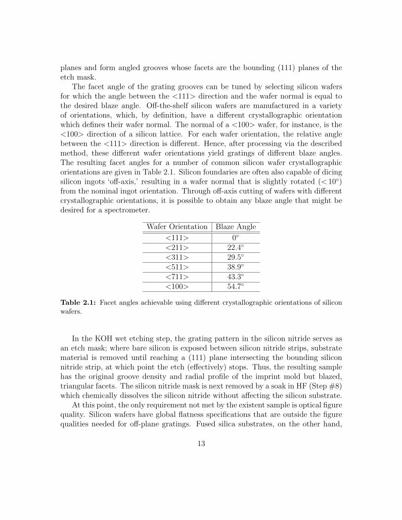
The facet angle of the grating grooves can be tuned by selecting silicon wafersfor which the angle between the <111> direction and the wafer normal is equal tothe desired blaze angle. Off-the-shelf silicon wafers are manufactured in a varietyof orientations, which, by definition, have a different crystallographic orientationwhich defines their wafer normal. The normal of a <100> wafer, for instance, is the<100> direction of a silicon lattice. For each wafer orientation, the relative anglebetween the <111> direction is different. Hence, after processing via the describedmethod, these different wafer orientations yield gratings of different blaze angles.The resulting facet angles for a number of common silicon wafer crystallographicorientations are given in Table 2.1. Silicon foundaries are often also capable of dicingsilicon ingots ‘off-axis,’ resulting in a wafer normal that is slightly rotated (< 10◦)from the nominal ingot orientation. Through off-axis cutting of wafers with differentcrystallographic orientations, it is possible to obtain any blaze angle that might bedesired for a spectrometer.
Wafer Orientation Blaze Angle
<111> 0◦
<211> 22.4◦
<311> 29.5◦
<511> 38.9◦
<711> 43.3◦
<100> 54.7◦
Table 2.1: Facet angles achievable using different crystallographic orientations of siliconwafers.
In the KOH wet etching step, the grating pattern in the silicon nitride serves asan etch mask; where bare silicon is exposed between silicon nitride strips, substratematerial is removed until reaching a (111) plane intersecting the bounding siliconnitride strip, at which point the etch (effectively) stops. Thus, the resulting samplehas the original groove density and radial profile of the imprint mold but blazed,triangular facets. The silicon nitride mask is next removed by a soak in HF (Step #8)which chemically dissolves the silicon nitride without affecting the silicon substrate.
At this point, the only requirement not met by the existent sample is optical figurequality. Silicon wafers have global flatness specifications that are outside the figurequalities needed for off-plane gratings. Fused silica substrates, on the other hand,
13

are optically flat to high precision and are relatively cheap. By imprinting the blazedsilicon grating into resist on a fused silica substrate (Step #9), the radially ruled,blazed grating profile can be replicated on a surface meeting the required figure. Asa secondary benefit, a second imprint makes the production of flight gratings a morecost- and time-effective process, as the same silicon grating can be used for multipleimprints, thus boosting process yield. As the resist on the fused silica will ultimatelycontain the desired grating pattern, it must be mechanically durable for flight andable to withstand the deposition of an X-ray reflective layer (Step #10) over topof the resist. Energetic ions impacting T-NIL resist during thin film deposition canoblate the imprinted pattern. In addition, these ions also deposit thermal energy intothe substrate, which can heat the thermal resist and alter the cured pattern. T-NILis also temporally unstable, losing its fidelity to the imprinted profile over time. UVnanoimprint lithography (UV-NIL), on the other hand, uses a liquid polymer whichcures after exposure to UV light and has significantly better mechanical and thermalstability, making it a better candidate for the second, final imprint. The depositionof a thin reflecting layer, such as gold, platinum, or iridium, concludes the fabricationprocess and yields an off-plane grating of flight quality.
2.1.3 Grating Production at Iowa
Using the described process, I have successfully made prototype off-plane gratingssimilar to those that would be used in a next-generation spectrometer. I obtainedthree types of wafers which yield different blaze angles: a <111> wafer cut 10◦ off-axis (10◦ facet angle), a <311> wafer (29.5◦ facet angle), and a <100> wafer (54.7◦
facet angle). These were processed through the HF soak step (Step #8 of Figure 3)at the UIMF, then sent on to Nanonex Corporation for the remaining imprint andreflective coating steps.
The grating mold employed for the imprint measures 32 mm × 25 mm, matchesthe convergence of a telescope with an 8.4 m focal length, has a 50% duty cycle,and has a groove density averaging2 6033 gr/mm. The grating template has beenextensively tested in X-rays and has demonstrated absolute diffraction efficiencies of> 40% (McEntaffer et al., 2013) and resolving powers > 3000 (McEntaffer, 2015).
Figure 2.2 shows Scanning Electron Microscope micrographs (SEMs) of severalin-process sample gratings. The current device ‘recipe’ for off-plane gratings withreference to the tools available at the University of Iowa Microfabrication Facility
2Note that due to radial ruling of the grating, the groove density changes along the optical axisof the grating. The number given here is the nominal groove density at the physical center of thegrating pattern.
14
(UIMF) is explicitly described in Appendix A. While this method has been success-fully used to fabricate blazed gratings, there are several drawbacks to the currentexecution of the manufacturing process which I briefly elaborate upon here.
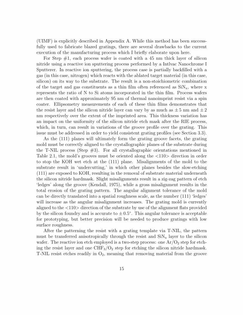
For Step #1, each process wafer is coated with a 45 nm thick layer of siliconnitride using a reactive ion sputtering process performed by a Intlvac Nanochrome ISputterer. In reactive ion sputtering, the process case is partially backfilled with agas (in this case, nitrogen) which reacts with the ablated target material (in this case,silicon) on its way to the substrate. The result is a non-stoichiometric combinationof the target and gas constituents as a thin film often referenced as SiNx, where xrepresents the ratio of N to Si atoms incorporated in the thin film. Process wafersare then coated with approximately 95 nm of thermal nanoimprint resist via a spincoater. Ellipsometry measurements of each of these thin films demonstrates thatthe resist layer and the silicon nitride layer can vary by as much as ± 5 nm and ± 2nm respectively over the extent of the imprinted area. This thickness variation hasan impact on the uniformity of the silicon nitride etch mask after the RIE process,which, in turn, can result in variations of the groove profile over the grating. Thisissue must be addressed in order to yield consistent grating profiles (see Section 3.3).
As the (111) planes will ultimately form the grating groove facets, the gratingmold must be correctly aligned to the crystallographic planes of the substrate duringthe T-NIL process (Step #3). For all crystallographic orientations mentioned inTable 2.1, the mold’s grooves must be oriented along the <110> direction in orderto stop the KOH wet etch at the (111) plane. Misalignments of the mold to thesubstrate result in ‘undercutting,’ in which other planes besides the slow-etching(111) are exposed to KOH, resulting in the removal of substrate material underneaththe silicon nitride hardmask. Slight misalignments result in a zig-zag pattern of etch‘ledges’ along the groove (Kendall, 1975), while a gross misalignment results in thetotal erosion of the grating pattern. The angular alignment tolerance of the moldcan be directly translated into a spatial roughness scale, as the number (111) ‘ledges’will increase as the angular misalignment increases. The grating mold is currentlyaligned to the <110> direction of the substrate by use of the alignment flats providedby the silicon foundry and is accurate to ± 0.5◦. This angular tolerance is acceptablefor prototyping, but better precision will be needed to produce gratings with lowsurface roughness.
After the patterning the resist with a grating template via T-NIL, the patternmust be transferred anisotropically through the resist and SiNx layer to the siliconwafer. The reactive ion etch employed is a two-step process: one Ar/O2 step for etch-ing the resist layer and one CHF3/O2 step for etching the silicon nitride hardmask.T-NIL resist etches readily in O2, meaning that removing material from the groove
15

sidewalls is difficult to prevent. The etch isotropy can be advantageous, however, asthe Ar/O2 etch can be used to narrow the resist plateaus, eventually resulting in athinner silicon nitride ‘tabs’ for the KOH etch mask and an increased duty cycle ofthe blazed grating. The subsequent CHF3/O2 etch step for the silicon nitride layer isalmost entirely anisotropic, but the (necessary) use of fluorine to remove the siliconnitride has the drawback that it will also etch into the underlying silicon substrate.The removal of substrate material results in a deeper groove trough; the removal oftoo much substrate material can lead to undercutting. Hence, non-uniformity in thesilicon nitride layer can yield a grating which has a duty cycle which varies over theoptical surface, or, worse, areas of the grating ‘undercut’ by the removal of too muchsubstrate material.
Finally, the chemical resistance of the deposited SiNx thin film to the bufferedHF solution is uncertain. Metrology up to this point has shown that there is a highdegree of variation resulting from similar (or even identical) buffered HF/KOH wetetch steps. Note the <111> 10◦ off-axis grating and the <311> grating in Figure2.2 are both shown prior to the HF soak step which completely removes the siliconnitride hardmask, yet the remaining ‘tabs’ of SiNx have very different appearances.Both of these substrates were exposed to identical buffered HF solutions for equaltimes.
2.2 Grating Performance Measurement
Of the three grating profiles produced via the off-plane grating microfabricationprocess, two have been tested in the X-ray to observe the resultant diffraction pattern.Both the <311> and the <111> 10◦ off-axis orientations were tested at the MaxPlanck Institute for Extraterrestrial Physics’ X-ray test facility, PANTER (Figure2.3). The PANTER facility consists of several X-ray fluorescence or monochromatorsources which are housed at one end of a 122 m long, 1 m diameter vacuum chamber,forming a long ‘beamline’ over which source light can be collimated. At the oppositeend, a 12 m long, 3.5 diameter instrument chamber is joined to the beamline andhouses a customizable optical bench manueverable with vacuum stages. Imaging andenergy-sensitive X-ray detectors are also housed in the instrument chamber. Theentire vacuum apparatus is capable of reaching pressures < 10−5 mbar. A schematicof our experimental set-up inside the instrument chamber is shown in Figure 2.4.
A custom silicon pore optic (SPO) mirror module was utilized to focus the in-coming beam prior to incidence on the tested gratings. SPO mirror modules areformed from superpolished silicon plates that have been diced to form small (∼ 1mm) channels. These plates are then stacked atop one another to form ‘pores’ which
16

permit X-rays to pass through. By elastically deforming the plates around an innermandrel and angling each subsequently stacked plate (‘wedging’), the mirrors can bebent into a conical approximation of paraboloids or hyperboloids, thus enabling theconstruction of a Wolter-I type telescope. SPO stacks with 45 plates have achievedhalf energy widths3 (HEW) of 15-17 arcseconds (Bavdaz et al., 2012). The SPOmirror module employed for this PANTER grating test was not a full Wolter-I, butinstead an 14 plate stack consisting of only paraboloids. The SPO mirror modulehas a nominal radius of curvature of 450 mm, but after construction was measuredto relax to 475 mm due to bending stress. The SPO has a focal length of ∼ 8.6 m atthe finite conjugate distance of the source. The aberration caused by the slight mis-match of the SPO focal length to the convergence of the grating is small comparedto the linespread function of the SPO.
An X-ray fluorescence source with a Mg target was used to measure the line-spread functions of the SPO focus and the diffracted orders for both gratings. Thegratings were aligned to the SPO focus and the rotation of the grating about itsnormal (the ‘yaw’ of the grating) zeroed. Each was then placed into the Littrowconfiguration for an incidence angle that enabled the sampling of multiple orders ofMg K (@ 1.254 keV) with the specified detector configuration. Functionally, reachingthe Littrow configuration involves setting the pitch (or incidence angle) and the yawof the grating: increasing the incidence angle serves to increase the radius of thearc, while increasing the yaw of the grating increases α. Recall that in the Littrowconfiguration, α = β = θ (Figure 1.2). Through Eq. 1.1 and Eq. 1.2, it is possibleto show that, in the Littrow configuration:
λblaze =2d tan γ tan θ
n. (2.1)
Manipulating the incidence angle of the grating thus enables the placement of a MgK order at the ideal β. The grating is then placed into the Littrow configuration bygiving it a yaw Ψ equal to:
Ψ = sin−1 (tan γ tan θ) , (2.2)
which can also be derived through geometric considerations.The groove facets of the <311> grating were blazed towards positive orders and
have an angle of θ = 29.5◦. While similar to the facet angles required for futurespectrometers (Smith, 2014a), limitations on stage travel precluded the possibility oftesting this grating at an incidence angle of γ = 1.5◦, the incidence angle baselined
3The half energy width of an optic is the diameter of the circle enclosing half the focused power.
17

for most future grating instruments4. Thus, the <311> was tested at an incidenceangle of 0.6◦, which places the Mg Kα +2nd order line near the location of highestdiffraction efficiency.
As the <111> 10◦ off-axis grating has a shallow facet angle of θ = 10◦, a testincidence angle of γ = 1.5◦ placed the ideal β in a location accessible to the focalplane detectors. However, this ideal β does not correspond to the wavelength of anyline fluoresced by the Mg target, lying just between the position of -1st and -2ndorder5 of Mg Kα.
Spectral information is extracted from the data by collapsing the image in thevertical (cross-dispersion) direction. Any potential offset in the azimuthal positionof the mirror relative to the grating normal (an effective ‘roll’ of the grating, seeFigure 3.1) will yield a rotated linespread function, broadening the observed line inwavelength space. This effect can be deconvolved from the data by fitting a line tothe linespread function of the 0th order image and deriving a rotation from the best-fit slope. This same rotation is then applied to the images of all diffracted orders forthat grating.
Rotated images of diffracted orders from the <311> grating are shown in Figure2.5, while those from the <111> 10◦ off-axis grating are shown in Figure 2.6. Thecollapsed linespread functions are fit with a Gaussian line profile. The data and fitsare normalized by equating the amplitudes of the Gaussian fits. The lines can thenbe compared side-by-side to determine the change in the linespread function fromthe spectral focus to the diffracted spot (Figure 2.7 for the <311> grating, Figure2.8 for the <111> 10◦ off-axis grating). The errors on the FWHM in Figures 2.7 andFigure 2.8 are derived from the Gaussian fits to the data and are 1σ errors.
The focus quality of the SPO in the cross-dispersion direction (∼ 3.9”) is toopoor to support measurements of high resolving power from these gratings. Never-theless, the measurements show that the linespread function observed in zero orderis largely preserved even at large β, thus precluding grating induced aberration atthis focus quality. Figs. 2.7 and 2.8 show that the spectular reflection from both the<311> and the <111> 10◦ off-axis grating is identical to the SPO focus to within3σ. Furthermore, the linespread functions of all diffracted orders are statisticallyindistinguishable from to their zero order counterparts at 3σ significance, with thenotable exception of two lines at high dispersion locations: the <111> 10◦ -3rd order
4Testing the <311> grating at an incidence angle of γ = 1.5◦ required 250 mm of stage travelfrom zero order; the PANTER test configuration used for this test supported approximately 100mm in the direction of the <311> blaze.
5Note that the groove facets for the <111> 10◦ were blazed towards negative orders, hence thechange in order ‘sign’ from the <311> diffracted orders to the <111> 10◦ off-axis diffracted orders.
18

line (3.2σ) and the <311>+2nd order line (3.5σ).There are known systematic errors which contribute to the broadening of the line-
spread function in the spectral direction at high dispersion locations. Optical pathlength differences due to the physical width of the grating and the curvature of thefocal plane are expected to be the dominant broadening effects for this optical config-uration, though other errors (e.g. the figure quality of the optic, the mismatch of theradial profile to the convergence of the telescope, etc.) are expected to contribute.These errors likely account for the systematic increase of the FWHM from zero orderto the diffracted orders and contribute to the broadening of the aforementioned linesoutside the 3σ significance threshold. Modeling the optical system via raytracing willclarify which broadening effects are expected to dominate. Given adequate statisticsin the observed lines, raytracing studies may also enable the deconvolution of theseerrors from the observed linespread function in order to establish an upper limit onany grating-induced aberration, an important result for gratings fabricated using thistechnique.
The PANTER measurements also empirically verify a significant premise of ourmicrofabrication studies: sculpting the groove profile through the microfabricationprocess can be used to change the efficiency response at a specified energy. Diffractionefficiency measurements show that at 1.25 keV (approximately the energy of MgKα), the efficiency of the grating mold in second order is nearly zero, owing to aninterference pattern between the groove trough and groove plateau (McEntaffer et al.(2013)). The <311> grating, identical to the mold save in the groove profile, is notonly demonstrated to have a non-zero response at Mg Kα +2nd order, but this lineis in fact 25% brighter than the +1st Mg K order line when operated in the Littrowconfiguration. Rigorous efficiency measurements of a blazed grating over a widerange of orders and energies should be made to quantitatively exhibit this finding;nevertheless, these PANTER measurements provide strong empirical evidence thatcustomizing the groove profiles of off-plane gratings can improve the effective areaof grating spectrometers at wavelengths of interest. Analysis of these measurementsis ongoing, and will conclude in a publication in Spring 2015 (see 3.6).
2.3 Optical Design of the OGRE Spectrometer
As discussed in Section 1.4, my thesis work also includes the optical design of theX-ray grating spectrometer onboard OGRE. OGRE will be the first astronomicalmission to fly customized off-plane gratings made from the microfabrication tech-nique described in Subsection 2.1.2. OGRE will also leverage a new X-ray mirrormanufacturing technique developed at Goddard Space Flight Center (GSFC), and
19

use a specialized charge-coupled device (CCD) detector to achieve unprecedentedperformance in the soft X-ray bandpass. Thus, OGRE represents an importantmilestone towards a future X-ray observatory, realizing spectral performance beyondthe capabilities of Chandra and XMM-Newton in an easily scalable, cost-efficientmeans.
OGRE will use a traditional Wolter-I style telescope consisting of thin single-crystal silicon mirrors to achieve an optical focus quality ∼ 2” in the dispersiondirection. Such a tight linespread function enables high resolutions even within thebounds of a suborbital rocket envelope. The manufacturing process for these mirrors(Zhang et al., 2014) begins with a block of cut silicon which has been chemicallyetched to remove any surface damage. Next, the desired optical shape is cut andthe surface polished using a commercially available polishing technique. The mirrorfigure can be tested and qualified at this point, allowing for the possibility of aniterative process to improve the mirrors focusing power over several polishing cycles.When the required figure is achieved, the optical surface is removed by slicing a thinface-sheet from the silicon block. This eliminates the excess silicon and serves tolightweight the mirrors. However, the cutting process creates surface damage on theback (convex) side of the mirror, which imposes new stress and distorts the figure.A chemical etch and/or annealing can remove this damage and should restore theoriginal figure.
In addition to employing these cutting-edge mirrors, OGRE will also make useof EM-CCDs at the focal plane, which have seen limited space-flight application upto this point but have immense promise as X-ray detectors (Tutt et al., 2014). Atthe low end of the soft X-ray bandpass (0.3 – 0.6 keV), the effective area of gratingspectrometers is mainly limited by detector effects. For one, X-ray photons have ahigh probability of registering as ‘split events,’ or spreading the liberated electronsover multiple pixels in a CCD. This serves to reduce the signal-to-noise ratio in a givenpixel. For soft X-ray photons, this split effect can dilute the signal below the noisethreshold, resulting in lost events. EM-CCDs have several advantages in detectingthese low energy X-ray photons. EM-CCDs differ in that the signal passes throughan electron multiplication register before chip readout, which serves to amplify theinput signal. As amplification occurs before the charge is output, readout noise issuppressed, and the overall signal-to-noise ratio of the device is improved. Thus, evensoft split X-ray events can be amplified above the noise threshold, greatly increasingthe detectability of low energy photons and helping to maintain high effective areasnear the soft energy cut-off.
These two critical technologies have been more throroughly discussed elsewhere(thin, single-crystal mirrors: Zhang et al. (2014) and references therein, EM-CCDs
20

for X-ray spectroscopy: Tutt et al. (2014)), and a broad overview of the OGREmission has already been provided (DeRoo et al., 2013). Creating an optical con-figuration which maximizes the performance of this unique spectrometer, however,is a non-trivial challenge that merits its own discussion. Firstly, realizing high per-formance within the payload envelope of a sounding rocket is difficult owing to therelative speed6 of the optical system. X-ray optical systems typically have focallengths on the order of 8 – 10 m – Chandra and XMM-Newton, for example, havefocal lengths of 10.0 m and 7.5 m respectively. On the other hand, in a soundingrocket, flight stability dictates an instrumental payload length less than 4.5 m. Thisimpacts the distance between the grating assembly and the focal plane L, resulting inless dispersion (Eq. 1.2), which can ultimately impact resolution. Secondly, the lim-ited payload diameter also impacts the radial extent of the mirror assembly. As thegeometric area of the mirror assembly provides an upper limit on the spectrometer’seffective area, achieving high effective areas in a rocket envelope is rarely as simpleas adding additional mirrors. Finally, the optical assembly must hold within align-ment tolerances over launch, which has greater accelerations than most observatorylaunches.
To design an optical assembly meeting the OGRE performance requirementswithin these instrumental bounds, a series of custom Python packages called Spect-Design was written. SpectDesign requires a set of input parameters which dictateimportant instrumental constraints, such as the focal length and radial extent ofthe mirror assembly, grating incidence angle, groove density, etc. and solves for thenumber of optics (paraboloids, hyperboloids, and gratings) as well as individual posi-tions of each optic required to build a given grating spectrometer. The instrumentalconfiguration can then be exported to a text file or to Solidworks for CAD rendering.The response of the instrumental configuration to source photons can also be sim-ulated with SpectDesign via ‘raytrace,’ in which individual photons are propagatedthrough an optical configuration geometrically. SpectDesign also includes scriptswhich incorporate phenomenological effects like scattering and diffraction, making itpossible to simulate the spectral locations of diffracted spots as well as the resolu-tions achieved by the instrument at a given wavelength. Finally, through the use oflibraries containing the X-ray reflectivities of different materials at various incidenceangles, the effective area of the configuration can be calculated. Even if raytracediteratively to build up a statistically significant (N ∼ 100) number of predicted instru-
6Formally, the focal length of the telescope divided by the aperture. For our purposes, take thisto be the ratio of the focal length to the inner radius of Wolter-I mirrors. A ‘fast’ telescope has asmall ratio, requiring a larger angle of convergence for the light to reach the focus. Note that even‘fast’ X-ray systems are ‘slow’ by optical telescope standards.
21

mental responses, the total time taken for each configuration calculation is less thanfifteen minutes, making it possible to iteratively explore the complex design spaceand obtain quantitative comparisons between different instrumental configurations.
SpectDesign positions and orients the gratings based on a mathematical construc-tion known as the Rowland circle. The Rowland formalism was originally derivedfor concave optical gratings and is a geometric construction ensuring that diffractedorders appear at the same spatial position at the focal plane, despite incidence atdifferent azimuths along the concave surface (Born and Wolf, 1999). In the X-ray, theRowland formalism is coopted into grazing incidence by using an array of gratings‘fanned’ along the azimuthal extent of the Rowland circle. By the geometry of theRowland formalism, the ideal focal plane is also curved, lying along a 3-dimensionaltoroidal surface7 defined by rotating the Rowland circle around the axis defined bythe telescope focus and the spectrometer focus (the zero order position). Gratingspositioned on the Rowland circle have been successfully used for the XMM-NewtonReflection Grating Spectrometer (den Herder et al. (2001)), and are the baselineoptical configuration for any off-plane grating spectrometer. Figure 2.9 shows theXMM-Newton and the OGRE Rowland circle designs.
Employing the Rowland circle to position the gratings for OGRE, however, il-lustrated a new issue for fast spectrometers. The Rowland formalism ensures thatorders are diffracted towards the same position on the focal plane; however, it makesno attempt to account for the difference in optical path length between reaching thetelescope focus and the spectral focus. Thus, diffracted light from different incidencelocations on the grating array may be intra- or extra- focal at the focal plane de-fined by the Rowland formalism, which then yields an aberration in the linespreadfunction.
The effect of this aberration can be seen in Figure 2.10, which shows the resolutionobtained via SpectDesign raytracing for a single OGRE module (focal length z0 =3500 mm, inner mirror radius R0 = 300 mm). The radial extent of the single moduleis then increased in increments of 25 mm and the resulting resolution calculated viaraytrace. The resolution is measured at 37.5 A, which at the focal plane is at the samelocation as third order 12.5 A, the approximate wavelength of a suite of bright Felines which will be observed by OGRE. Obviously, the azimuthal extent of the gratingarray must grow as the radial extent of the Wolter-I telescope increases in order tocontinue to intercept all of the converging beam. However, the outermost gratings,i.e. the positions with the greatest azimuthal difference from the center grating,have the greatest path length difference from telescope to spectral focus. Hence,there is a direct trade-off between resolution and effective area: as the effective area
7sometimes known as the Rowland torus
22
grows by increasing the geometrical area of the telescope, the optical path lengthdifference also increases and degrades the instrumental resolution. This problemwith the Rowland circle placement is exacerbated by the fast OGRE telescope - therelatively short focal length requires a more rapidly converging beam, which in turnyields a less focused beam when sampled intra-/extra-focally.
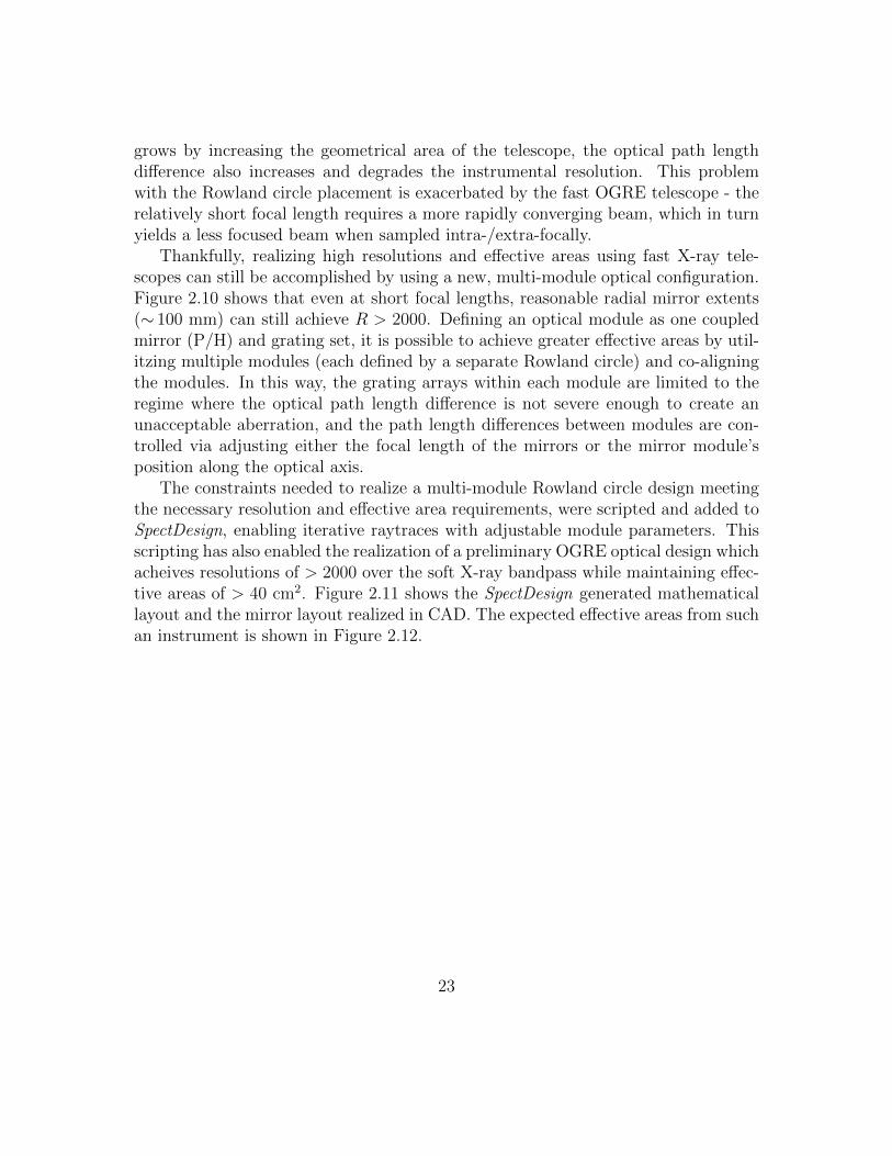
Thankfully, realizing high resolutions and effective areas using fast X-ray tele-scopes can still be accomplished by using a new, multi-module optical configuration.Figure 2.10 shows that even at short focal lengths, reasonable radial mirror extents(∼ 100 mm) can still achieve R > 2000. Defining an optical module as one coupledmirror (P/H) and grating set, it is possible to achieve greater effective areas by util-itzing multiple modules (each defined by a separate Rowland circle) and co-aligningthe modules. In this way, the grating arrays within each module are limited to theregime where the optical path length difference is not severe enough to create anunacceptable aberration, and the path length differences between modules are con-trolled via adjusting either the focal length of the mirrors or the mirror module’sposition along the optical axis.
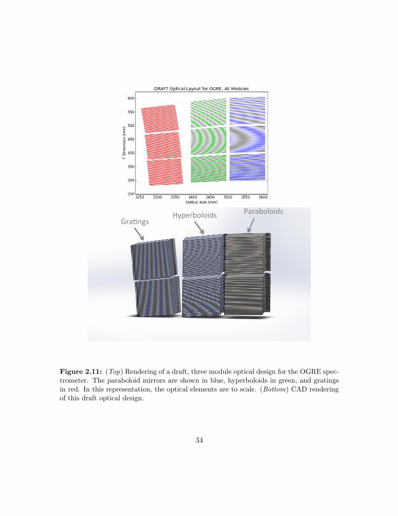
The constraints needed to realize a multi-module Rowland circle design meetingthe necessary resolution and effective area requirements, were scripted and added toSpectDesign, enabling iterative raytraces with adjustable module parameters. Thisscripting has also enabled the realization of a preliminary OGRE optical design whichacheives resolutions of > 2000 over the soft X-ray bandpass while maintaining effec-tive areas of > 40 cm2. Figure 2.11 shows the SpectDesign generated mathematicallayout and the mirror layout realized in CAD. The expected effective areas from suchan instrument is shown in Figure 2.12.
23

95 nm of resist!45 nm of SiNx!
Si wafer!
Native SiO2!
2) Prepare mold
3) Imprint into resist
T-NIL Resist!Silicon Nitride!
Si Wafer!
Native SiO2!
1) Spin coat wafer
5) Acetone rinse to remove residual resist
6) Buffered HF Dip to remove native SiO2
4) RIE through SiNx layer
8) HF soak
9) Imprint into UV resist
7) Timed KOH etch
UV-NIL Resist
Fused Silica Substrate
Figure 2.1: Procedure for fabricating off-plane gratings.
24
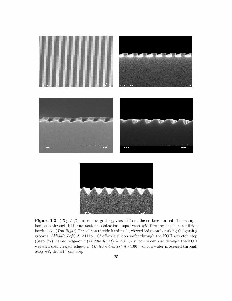
Figure 2.2: (Top Left) In-process grating, viewed from the surface normal. The samplehas been through RIE and acetone sonication steps (Step #5) forming the silicon nitridehardmask. (Top Right) The silicon nitride hardmask, viewed ‘edge-on,’ or along the gratinggrooves. (Middle Left) A <111> 10◦ off-axis silicon wafer through the KOH wet etch step(Step #7) viewed ‘edge-on.’ (Middle Right) A <311> silicon wafer also through the KOHwet etch step viewed ‘edge-on.’ (Bottom Center) A <100> silicon wafer processed throughStep #8, the HF soak step.
25
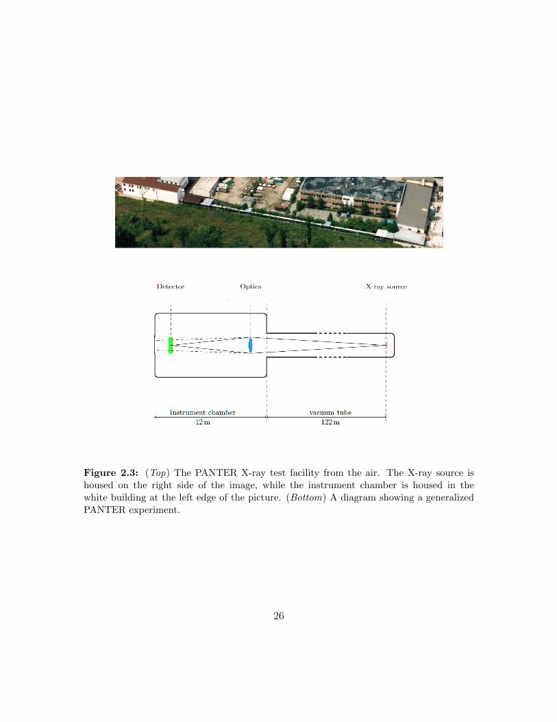
Figure 2.3: (Top) The PANTER X-ray test facility from the air. The X-ray source ishoused on the right side of the image, while the instrument chamber is housed in thewhite building at the left edge of the picture. (Bottom) A diagram showing a generalizedPANTER experiment.
26

Figure 2.4: Diagram of the off-plane grating test setup in the instrument chamber atPANTER. An SPO mirror module intercepts the incoming light from the X-ray sourceand focuses it at a point displaced in the +x direction (termed ‘Wald’ at PANTER). Thegratings then intercept this focused beam, reflecting it towards -x (‘Pantolsky’). Dispersionoccurs along the y axis. By way of an example, the diffraction pattern of Cu-L (@ 0.928keV) is shown at the bottom.
27

Figure 2.5: CCD measurements of the SPO focus, the spectral focus (0th order), and thediffracted spots from the <311> grating. All of these images were taken with the TRoPICcamera. 28
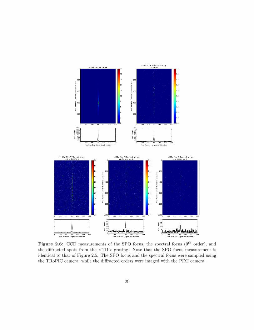
Figure 2.6: CCD measurements of the SPO focus, the spectral focus (0th order), andthe diffracted spots from the <111> grating. Note that the SPO focus measurement isidentical to that of Figure 2.5. The SPO focus and the spectral focus were sampled usingthe TRoPIC camera, while the diffracted orders were imaged with the PIXI camera.
29

Figure 2.7: Side-by-side comparisons of the SPO focus and spectral focus (Top) and thespectral focus and diffracted orders (Bottom) for the <311> grating.
30

Figure 2.8: Side-by-side comparisons of the SPO focus and spectral focus (Top) and thespectral focus and diffracted orders (Bottom) for the <111> 10◦ off-axis grating. Notethat for Mg K -3rd order, there are a low number of events (N < 100) contributing to thelarge fit errors. 31

Figure 2.9: (Top) The Rowland circle design for XMM-Newton (den Herder et al., 2001,Fig. 1). (Bottom) An example of a similar Rowland circle design for OGRE, as outputby SpectDesign. Note that the OGRE design is not to scale. The paraboloid mirrors areshown in blue, hyperboloids in green, and gratings in red, while the dashed red line outlinesthe fictional Rowland circle.
32
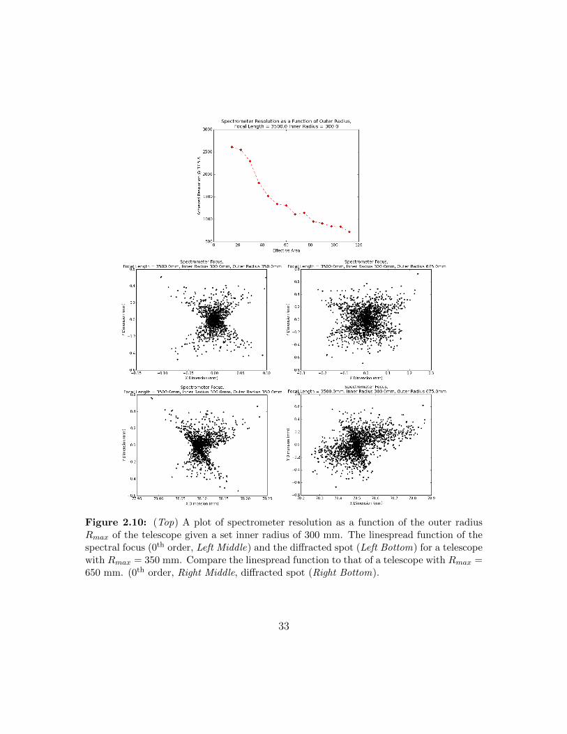
Figure 2.10: (Top) A plot of spectrometer resolution as a function of the outer radiusRmax of the telescope given a set inner radius of 300 mm. The linespread function of thespectral focus (0th order, Left Middle) and the diffracted spot (Left Bottom) for a telescopewith Rmax = 350 mm. Compare the linespread function to that of a telescope with Rmax =650 mm. (0th order, Right Middle, diffracted spot (Right Bottom).
33
Gra$ngs Hyperboloids Paraboloids
Figure 2.11: (Top) Rendering of a draft, three module optical design for the OGRE spec-trometer. The paraboloid mirrors are shown in blue, hyperboloids in green, and gratingsin red. In this representation, the optical elements are to scale. (Bottom) CAD renderingof this draft optical design.
34

Figure 2.12: The effective area of the draft OGRE optical design as a function of photonenergy.
35

Chapter 3
Work To Be Accomplished
For my thesis project, I anticipate accomplishing several more significant milestonesalong the road to the construction and flight of a cutting-edge grating spectrometer.For one, a theory of grating groove customization ought to be developed to guide theoptimizaton process for future mission architectures. Next, the OGRE optical designought to be completed in a timely fashion in order to guide the engineering effortalready underway and provide process requirements for the OGRE flight gratings,mirrors, and detector. Finally, the OGRE gratings will need to fabricated, charac-terized, and aligned within a flight module within the next two years in order to stayon the current mission schedule.
3.1 Theory of Grating Customization
As the fabrication technique described in Subsection 2.1.2 enables the manufacture ofgratings with a variety of groove densities and blaze angles, it remains to choose theoptimal groove profile for the spectroscopy mission in question. It is well-known thatthe Littrow configuration yields the maximum diffraction efficiency for a given wave-length. From a broader mission standpoint, however, it is rare that a spectroscopymission needs high efficiency at just a narrow range of wavelengths. Moreover, whilethe fabrication process itself is generalizable, in practice, constructing a variety ofgrating profiles for pre-mission evaluation is neither time- nor cost-effective. Forinstance, the grating imprint mold, from which the grating groove density is set,involves e-beam tooling which can require days of tool time and cost upwards of$100,000 to perform commercially. Hence, having the ability to quantitatively com-pare the diffraction efficiency of off-plane gratings prior to their fabrication (i.e.theoretically) is a necessity for future grating spectroscopy missions.
36

Calculations of the diffraction efficiency for gratings in a variety of mountingconfigurations, including the off-plane mount, have been performed by a number ofdifferent authors (see, for example, Loewen et al. (1977) , Goray and Seely (2002)).It is rare, however, that an author’s published efficiency curve pertains to the gratingcomparison at hand. Our group purchased commerical software, PCGrate, which iscapable of calculating grating diffraction efficiency for arbitary groove profiles. I usedPCGrate to model the measured diffraction efficiency of the grating mold, but wasunable to find a satisfactory fit to the mold efficiency data. The method PCGrateemploys to calculate diffraction efficiencies is also somewhat ambiguous, owing inpart to our lack of knowledge of diffraction theory. Achieving a more comprehensiveunderstanding of the diffraction from first principles is a necessary first step to betterutilize PCGrate and enable the comparison of diffraction efficiencies. This will beachieved by a literature review of grating efficiency calculations, and result in adetailed theory section in my final thesis document.
Next, in order to base grating construction decisions on the calculated values,verfiying the accuracy of the PCGrate efficiencies is paramount. This can be accom-plished in two ways: either by developing a robust way to fit the measured empiricalvalues with PCGrate through reasonable1 variations in the grating groove profile orwriting my own script to calculate grating diffraction efficiencies. Both of these pathsare informed by the previous literature review.
Finally, this method should be used to predict the efficiency of the OGRE flightgratings prior to their manufacture. In the ideal case, SEM/AFM measurements ofthe groove density, surface roughness, groove profile, etc. would be translated intoappropriate input parameters and a range of possible efficiencies found. Subsequentefficiency measurements (see Section 3.4) will allow for side-by-side comparison –if the measured efficiencies fall within the predicted range, it will serve as strongevidence that method of calculation can be used to support manufacturing decisionsin future missions. The comparison of theoretical and measured efficiencies will beincorporated into a larger paper describing the manufacture and testing of the OGREflight gratings.
1‘reasonable’ being within the errors offered by physical measurements of the grating in question.Scanning Electron Microscope (SEM) and Atomic Force Microscopy (AFM) measurements canconstrain the grating groove profile.
37
3.2 OGRE Optical Design Optimization
While a workable OGRE optical design has been found, the optical configuration hasyet to be optimized for OGRE performance. The current OGRE design was found byadjusting the outer radii of the three mirror modules to maximize the total geometricarea of the telescope while maintaining spectral resolving powers of R > 2000. Thelimiting factor in obtaining higher effective areas via this optimization process isthe payload diameter. The telescope was extended from the default mirror innerradius R0 (300 mm) radially outward until reaching the payload exterior skin on oneside; however, the default grazing incidence angle (γ = 1.5◦), requires the offset ofthe entire telescope assembly from the side directly opposite the outermost mirrorby ∼ 180 mm. This leaves ‘empty’ geometric area that could be used, but only byadjusting the grating incidence angle, the inner telescope radius, and/or the anglebetween the optical axis and the instrument axis. Optimizing the design beyond thispoint is a non-trivial problem, as these parameters are highly coupled to number ofoptics needed, the effective area yield per optical segment, the ultimate resolution ofthe telescope, etc. In this complex parameter space, finding an optical design thatyields the highest possible performance is a problem ideally suited for the iterativeapproach of SpectDesign.
First, a suitable optimization metric must be defined. To do this, papers reportingprevious observations of Capella will be consulted to find high science-yield and/oryet unresolved diagnostic lines. By factoring together the resolutions achieved atthese wavelengths, as well as the number of photons that would be collected overthe OGRE’s short observation window, it is possible to create a metric that ensuresmaximal OGRE science return. Assessing this metric for a variety of optical designsis slightly more difficult. Changing R0 and γ changes the location of the spectrometerfocus relative to the optical modules, shifting the ideal location for optical moduleplacement from iteration to iteration. Thus, new SpectDesign scripts will have tobe written to dynamically construct the best spectrometer within the ‘hard’ boundsof the payload envelope given the current parameter values within the scan. As thediffraction efficiency will also change at different grating incidence angles, this op-timization will also involve either 1) calculating the diffraction efficiency in situ, 2)consulting a preconstructed library of diffraction efficiencies via look-up tables, or 3)demonstrating that the diffraction efficiency does not change appreciably over thescan range of interest. Finally, as a check on the optimization routine, a full raytrac-ing simulation of the OGRE spectrometer should be completed. Such a simulationshould begin with an ideal source spectrum of Capella derived from the X-ray mod-eling package XSpec, and propagate those source photons through the final optical
38
design to yield a sample physical output at the focal plane. Ideally, this simulationwould take into account real uncertainties in the instrument (optical misalignmentswithin tolerance, X-ray split events, etc.) and during flight (off-axis pointing, point-ing drift, etc.). Having such a script in hand would be a powerful tool for futuremissions, as well as leave the OGRE team well-equipped to assess the impact of anychanges or engineering constraints that arise during construction of the payload.
3.3 Fabrication of a Flight-like Grating
The final optical design will dictate the precise requirements for the OGRE flightgratings. Nonetheless, the preliminary design has already elucidated several processrequirements which will necessate the further development of the off-plane gratingmicrofabrication technique so far employed. For one, the preliminary optical designshows that a facet angle ∼ 30◦ will be needed to obtain high effective areas in focalplane locations farthest from zero order (and hence yielding the highest resolutionsthat would be measured by OGRE). This in turn means that OGRE flight gratingswill ultimately be most similar to the fabrication process for <311> gratings. TheOGRE groove densities will remain in the 6000 gr/mm range, as the OGRE focalplane is of limited extent (≈ 150 mm) and the higher dispersions afforded by increasedgroove density will only serve to decrease OGRE’s bandpass while yielding little inincreased resolving power. Finally, to maximize instrumental effective area, theOGRE gratings must measure approximately 100 mm along the optical axis by 150mm wide in order to intercept all of the focused light of the mirror modules. Thelarger format requires moving to 6” diameter wafers, which may introduce addedcomplexity to the spin coating, imprinting, and wet etching steps.
In addition, there are several new elements to be considered during the fabricationprocess in order to yield gratings of high fidelity. For one, a new series of gratingmolds must be manufactured to yield the correct convergence for OGRE. McEntafferet al. (2013) describes the mold manufacturing process in detail; we will concernourselves here only with the writing of the mold pattern. Upon reaching a finaloptical design, SpectDesign will output grating pattern that must then be transferredinto a CAD design. This CAD design will then be input into an electron beam (e-beam) lithography tool and written on an ultra-flat fused silica substrate coated withchromium and photoresist. It is our intent to perform the e-beam writing in housewith the new Raith Voyager e-beam tool, which has been purchased by the Universityof Iowa and will be installed by Spring 2015. Performing the e-beam lithographystep in-house will yield significant cost savings (∼ $100,000) for the OGRE mission.In addition, this experience enables the prototyping of gratings for future, larger
39

missions cheaply and quickly.The OGRE grating fabrication process must consistently yield the same groove
profile – to accomplish this, the silicon nitride hardmask must be consistent from sam-ple to sample. A CVD coating of silicon nitride will not only have a more consistentthickness across the (now larger) imprinted area than the silicon nitride depositedvia reactive ion sputtering, but should also offer better chemical resistance to thebuffered HF solution. Moving to this industrial standard also decreases the numberof processing steps performed at Iowa, decreasing time spent per wafer and puttingmore of the fabrication procedure in the hands of industrial partners2. Changingthe hardmask may require recharacterizing the current CHF3/O2 RIE step, an issueI anticipate solving on smaller, less expensive <311> wafers first before moving toflight-like gratings.
A high fidelity flight grating will also necessitate better alignment of the T-NILmold to the <110> direction of the substrate. KOH etch ‘ledges’ along the grooveadd to the surface roughness of the grating surface and contribute to scattering.Furthermore, the flat plateaus between angled facets strengthen the zero order sig-nal at the expense of the diffracted orders; the highest diffraction efficiencies will beachieved by gratings without significant plateaus3. Yet the need for small plateausincreases the alignment precision needed to not etch under the silicon nitride hard-mask. The current alignment technique is good enough to not grossly undercut themask in most cases but is far from consistent: multiple <100> and <311> sampleshave been undercut despite being processed in an identical fashion as samples thatyielded normal grating profiles.
To achieve better mold/substrate alignment, I propose to perform an initial KOHetch of a small section of the substrate prior to the first imprint step to determinethe true orientation of the substrate’s crystalline planes. To perform this alignmentstep, a layer of positive photoresist would first be put down over top of the substrate.Next, a specially shaped photomask would be used to expose the resist in an areaof the substrate that will ultimately be outside the grating area. The photomaskpattern would be a series of lines, overlapping in their center and angularly fannedin a circle, like the spokes of a wagon wheel. After UV exposure, the resist wouldbe processed and the ‘wagon wheel’ transferred through the silicon nitride layer via
2A manufacturing process that largely involves the use of industrial partners is often considereda strength in astronomical mission proposals. Hence, by making the move now, it is possible torealize the aforementioned benefits as well as strengthen the proposal case for future missions.
3Compare Figure 2.2, the middle right inset vs. the bottom center inset. The bottom inset hasalmost no plateau between angled facets, while for middle right inset, the plateaus are approximately30% of the groove spacing and do not contribute efficiently to diffraction.
40
RIE, taking care to ensure that the eventual hardmask layer is not etched duringthis step. A KOH etch step is then performed and the spokes examined underan optical microscope. As the spokes are radially fanned, a wide range of possiblecrystallographic orientations are probed. The spoke with the cleanest, least undercutetch then indicates the <110> direction to within the tolerance of the spoke fanangle. As the flat orientation does not vary within a specified wafer batch, it wouldbe possible to buy an entire silicon ingot of the desired crystallographic orientation,perform the ‘wagon wheel’ etch for a random set of wafers in the batch, measure therelative angle between the ‘clean’ KOH etch groove and the wafer flat, and use thismeasurement to align the T-NIL imprint for each wafer in that batch. This techniquehas been demonstrated to achieve angular tolerances of 0.05◦ (Chang, 2004).
Fabricating the first OGRE flight grating represents a large portion of the here-outlined thesis work. First, the off-plane grating microfabrication process will befurther refined using relatively cheap <311> 3” wafers. These wafers will be coatedwith a CVD silicon nitride layer and used to characterize and, if necessary, tweak,the CHF3/O2 RIE etch used to transfer the grating pattern down to the substrate.These wafers will also be used to study the alignment procedure of the grating moldto the substrate crystalline planes using the described ‘wagon wheel’ method. Aftersuccessful development of a reliable alignment method, the entire process will beused to produce a completed <311> grating on silicon. The resulting grating willbe characterized in terms of groove profile, facet roughness, lithographic fidelity,etc. and if appropriate, measured for diffraction efficiency and resolving power.At this point, the OGRE optical design will be finalized and an order for the 6”OGRE substrates placed. Meanwhile, the grating pattern will be rendered in CAD,written via e-beam lithography and sent on to LightSmyth, an industrial partner, forsubsequent processing. In the meantime, the OGRE substrates will arrive, which willenable early studies of T-NIL resist thickness on 6” substrates, the characterization ofthe crystalline plane orientation via the ‘wagon wheel’ process, etc. LightSmyth willnext return a series of OGRE-specific molds, which will then be used to fabricatethe OGRE flight gratings using the developed process. Upon fabricating gratingswith acceptable profiles, these will be shipped to Nanonex for the completion ofSteps #9 and #10. After completion of the UV-NIL imprint and reflective coating,Nanonex will send the fused silica gratings to Sydor Optics, the vendor for thefused silica substrates, who will dice out the grating pattern from the substrate toyield rectangular flight gratings. I anticipate producing approximately 20 silicongratings for OGRE, which will be used to produce 100 – 300 fused silica gratings. Ialso anticipate performing this work in two phases, such that I will receive severalprototype gratings which have been processed all the way through the production
41

chain prior to the delivery of the bulk of the flight gratings.
3.4 Performance Testing of a Flight-like Grating
When fabricated, the OGRE flight gratings will be the most sophisticated X-ray off-plane gratings ever manufactured. As such, characterizing the performance of thefabricated gratings is not only important for OGRE, but an essential component inany program enabling the next generation of X-ray grating spectrometers. To thatend, I will test the flight gratings for both diffraction efficiency and resolving power.
A test campaign to measure the diffraction efficiency testing of the OGRE flightgratings will be conducted at the Physikalisch-Technische Bundesanstalt (PTB) softX-ray beamline at the BESSY II synchrotron (Laubis et al., 2009). X-ray radiationfrom the electron storage ring is sampled by the beamline, and a grating monochro-mator is used to tune the beam to a specified energy between 0.1 – 1.9 keV. Theoptic is mounted on a stage in the test chamber which has six degrees of freedom,a critical feature for aligning off-plane gratings for a given test configuration. Aphotodiode capable of scanning in two dimensions is then used to sample the focalplane. By selecting the beam energy, positioning the photodiode at the location of agiven order, and measuring the response of the photodiode, the diffraction efficiencyof the grating in all non-evanescent orders can be mapped over energy space. For theOGRE flight gratings, I will measure the diffraction efficiency of the gratings at thenominal (0◦ yaw) and in the Littrow configuration at the incidence angle specifiedby the OGRE design and at γ = 1.5◦ in order to be directly comparable to previousgrating efficiency measurements performed at BESSY (McEntaffer et al., 2013; Tuttet al., 2015)
Following the BESSY campaign, I will test the resolving power of an OGRE flightgrating at the NASA Marshall Space Flight Center’s Stray Light Facility (SLF).The SLF consists of an electron impact X-ray source, a 100 m long beamline tocollimate the source flux, and a 10 m long, 3 m diameter instrument chamber tohouse configurations of X-ray optics. The OGRE flight gratings will be tested inconjunction with a prototype OGRE mirror module manufactured by GSFC, whichwill create a focused X-ray beam with a convergence angle matching that of the flightgratings. This will be the first resolution measurement with blazed off-plane gratingsfabricated via the method described in Section 2.1.2. A summary of the flight gratingfabrication, diffraction efficiency measurements, and resolution measurements willthen be reported in a publication.
42

3.5 Construction of a OGRE Flight Module
The culmination of this thesis effort is the construction of one aligned and flight-readygrating module for the OGRE spectrometer. Studies of off-plane grating alignmentinto a single module (Marlowe et al., 2015; Allured et al., 2015) are underway, buthave thus far not achieved full alignment of the arcs of diffraction at the focal planenor aligned more than two gratings. Thus, while the construction of a flight gratingmodule benefits significantly from previous endeavors, it nonetheless represents asignificant step towards realizing a next generation X-ray grating spectrometer.
Constructing the flight module first requires the production of at least 20 – 40fused silica gratings. The flight housing will also need to be designed and built. Thegrating module will be fabricated from a specialized material, likely either Kovar tominimize the thermal expansion of the module over the course of flight or siliconcarbide to match the coefficient of thermal expansion of the gratings. The flighthousing will have wide slots cut at the nominal position of each grating, allowing forthe position and orientation of the gratings to be fine-tuned after gross placement.Next, the gratings need to be qualified before integration into a flight module, as thegratings will be permanently bonded to the module. The qualification process maytake the form of a visual inspection for gratings with poor imprint fidelity, an opticalfigure measurement, or even a simplified X-ray diffraction measurement. Either afteror during qualification, the angle between the grating pattern and the diced substrateedge will also need to be measured with an optical microscope. The UV-NIL imprintboundary can be seen with the naked eye and is parallel to the central groove ofthe grating pattern. Knowing this angular offset is essential to aligning the gratingabout its normal without X-ray testing.
Next, each individual grating must be inserted into the module and correctlyaligned in three spatial (x, the dispersion direction, y, the cross-dispersion direction,and z, the optical axis) and three rotation dimensions (pitch, the grating incidenceangle, roll, grating rotation in the xy plane, and yaw, rotation about the grating nor-mal; see Figure 3.1). This is performed with a specialized grating alignment assembly(Figure 3.2) mounted to an optical bench. A hexapod stage with six degrees of free-dom is employed to position the grating within its mounting slot in the flight module.The flight module itself is mounted to a translation and tilt assembly, which servesto index each grating slot in the flight module. A coordinate-measuring machine(CMM) and a theodolite sample the grating face to provide position/orientation in-formation. Each grating will be held by a set of six alignment flexures bonded to theouter edges of the grating. These flexures are then bonded to the grating moduleitself via holes in the module exterior. This alignment apparatus will be assembled
43

in a cleanroom environment so as to keep the optics free of particulate and molecularcontamination.
When the alignment of the flight gratings has been completed, the grating modulewill be aligned to the corresponding mirror module, and mark the completion one fullset of OGRE optics. Next, a systems-level test of the single OGRE optical modulewill be completed, either in an evacuated rocket skin on-site or at a facility with abeamline of appropriate length. A beamline test would be preferred, as this offersthe opportunity to test the OGRE optical configuration in a regime where the sourcedistance is much longer than the focal length of the system, thus approximating an‘source at infinity’ (like an astronomical source). However, traveling to a beamlinerequires a significant investment of personnel time, and may not be possible at thatpoint in the mission schedule and/or prior to the conclusion of this research. Testingthe OGRE optics within the evacuated exterior skin of the rocket payload is anacceptable alternative, provided that source is placed a sufficient distance away fromthe optics modules. Testing within the rocket skin allow will allow the use of theOGRE detectors and be the first systems-level test of the entire OGRE instrument.
3.6 Thesis Summary
To summarize, this thesis will yield the following five scientific contributions to thenext generation of X-ray reflection grating spectrometers:
1. A theoretical study of grating groove customization, with the goal of guidingthe design choices for future off-plane X-ray grating instruments
2. A completed optical design for a grating spectrometer using a fast X-ray tele-scope
3. A well-characterized fabrication method for making high-fidelity off-plane X-ray gratings at custom facet angles
4. Data showing the resolution and efficiency performance of an off-plane X-raygrating fabricated using the aforementioned technique
5. An aligned and characterized grating module for the OGRE sounding rocketflight
44

Figure 3.1: The grating coordinate system showing three spatial dimensions (x, y, z ) andthree rotational dimensions (pitch, roll, yaw).
45

Figure 3.2: An example of a grating alignment assembly that could be used to positionthe OGRE gratings in the flight module. The CMM laser apparatus and theodolite areoutside the picture, but can access the grating’s optical surface.
46

Chapter 4
Proposed Timeline of Study
The thesis work described herein will be completed over the course of the next twoyears. An approximate schedule is as follows:
Spring 2015
• Complete analysis of first fabricated grating results (PANTER testing, seeSection 2.2); write and publish paper.
• Optimize OGRE optical design and calculate nominal alignment toler-ances; present finished design to OGRE instrument team
• Begin literature review of grating efficiency calculations
Summer 2015
• Characterize new CVD silicon nitride coating in grating fabrication pro-cess; develop new RIE recipe if required
• Develop new T-NIL mold alignment procedure
• Fabricate <311> grating using current (z0 = 8.4 m) mold
• Translate OGRE grating pattern to CAD
Fall 2015
• Write OGRE grating pattern onto replication mask using Iowa e-beamlithography tool; send mask to LightSmyth for mold production
• Order silicon substrates for OGRE production
• Write grating efficiency calculation scripts; search for a reliable methodof fitting measured efficiencies with theoretical models
47

• Simulate OGRE instrument response during 300 second observation ofCapella, derive alignment tolerances through SpectDesign scripting
Winter 2015
• Receive OGRE substrates and grating molds
• Fabricate flight-like OGRE grating on silicon
• Design flight grating module and grating module alignment apparatus
• Conclude theoretical modeling work; publish if appropriate
Spring 2016
• Send silicon flight-like grating to Nanonex/Sydor Optics for completion;receive flight-like fused silica OGRE gratings
• Begin mass-production of flight-like OGRE gratings on silicon
• Measure diffraction efficiency of flight-like OGRE grating on fused silica
• Manufacture and assemble OGRE grating module, grating module align-ment apparatus
Summer 2016
• Measure resolving power of flight-like, fused silica OGRE gratings
• Receive mass-produced, fused silica OGRE gratings from Nanonex/SydorOptics
• Develop qualification method for fused silica OGRE gratings; measureangle between imprint and diced edge
• Study grating alignment technique using grating module alignment appa-ratus, engineering modules
Fall 2016
• Align fused silica OGRE gratings into grating module
Winter 2016
• Finish construction and alignment of OGRE grating module
• Begin writing dissertation
Spring 2017
48

• Measure the performance of the integrated OGRE optics module at suit-able facility
• Finish writing dissertation
• Defend and graduate
49

Bibliography
Allured, R., Donovan, B., Burwitz, V., DeRoo, C., Marlowe, H., Menz, B.,Miles, D., Tutt, J., and McEntaffer, R.: 2015, forthcoming
Allured, R. and McEntaffer, R. T.: 2013, Experimental Astronomy 36, 661
Bavdaz, M., Wille, E., Wallace, K., Shortt, B., Collon, M., Ackermann, M.,Riekerink, M. O., Haneveld, J., van Baren, C., Erhard, M., Christensen,F., Krumrey, M., and Burwitz, V.: 2012, in Society of Photo-Optical In-strumentation Engineers (SPIE) Conference Series, Vol. 8443 of Society ofPhoto-Optical Instrumentation Engineers (SPIE) Conference Series, p. 29
Born, M. and Wolf, E.: 1999, Principles of Optics, Cambridge UniversityPress, 7th edition
Bregman, J. N.: 2007, Annual Review of Astronomy and Astrophysics 45, 221
Cash, Jr., W. C.: 1983, Applied Optics 22, 3971
Cash, Jr., W. C.: 1991, Applied Optics 30, 1749
Chandra Project Science, MSFC: 2014, The Chandra Proposers’ ObservatoryGuide, Chandra X-ray Center, 60 Garden Street, Cambridge MA 02138,Version 17.0
Chang, C.-H.: 2004, Master’s thesis, Massachusetts Institute of Technology
den Herder, J. W., Brinkman, A. C., Kahn, S. M., Branduardi-Raymont, G.,Thomsen, K., Aarts, H., Audard, M., Bixler, J. V., den Boggende, A. J.,Cottam, J., Decker, T., Dubbeldam, L., Erd, C., Goulooze, H., Gudel, M.,Guttridge, P., Hailey, C. J., Janabi, K. A., Kaastra, J. S., de Korte, P. A. J.,van Leeuwen, B. J., Mauche, C., McCalden, A. J., Mewe, R., Naber, A.,Paerels, F. B., Peterson, J. R., Rasmussen, A. P., Rees, K., Sakelliou, I.,
50

Sako, M., Spodek, J., Stern, M., Tamura, T., Tandy, J., de Vries, C. P.,Welch, S., and Zehnder, A.: 2001, Astronomy & Astrophysics 365, L7
DeRoo, C. T., McEntaffer, R. L., Schultz, T., Zhang, W. W., Murray, N. J.,O’Dell, S. L., and Cash, W.: 2013, in Society of Photo-Optical Instrumen-tation Engineers (SPIE) Conference Series, Vol. 8861 of Society of Photo-Optical Instrumentation Engineers (SPIE) Conference Series
Goray, L. I. and Seely, J.: 2002, Applied Optics 41(7), 1434
Kendall, D. L.: 1975, Applied Physics Letters 26(4), 195
Laubis, C., Scholze, F., Bucholz, C., Fischer, A., Hesse, S., Kampe, A., Puls,J., Stadelhoff, C., and Ulm, G.: 2009, in Society of Photo-Optical Instrumen-tation Engineers (SPIE) Conference Series, Vol. 7271 of Society of Photo-Optical Instrumentation Engineers (SPIE) Conference Series
Loewen, E. G., Neviere, M., and Maystre, D.: 1977, Applied Optics 16(10),2711
Marlowe, H., Allured, R., DeRoo, C., Miles, D., Donovan, B., Tutt, J., Menz,B., Burwitz, V., Hartner, G., and McEntaffer, R.: 2015, forthcoming
McEntaffer, R., DeRoo, C., Schultz, T., Gantner, B., Tutt, J., Holland, A.,O’Dell, S., Gaskin, J., Kolodziejczak, J., Zhang, W. W., Chan, K.-W.,Biskach, M., McClelland, R., Iazikov, D., Wang, X., and Koecher, L.: 2013,Experimental Astronomy 36, 389
McEntaffer, R. L.: 2015, forthcoming
Smith, R. K.: 2014a, in AAS/High Energy Astrophysics Division, Vol. 14 ofAAS/High Energy Astrophysics Division
Smith, R. K.: 2014b, Arcus: Exploring the Formation and Evolution of Clus-ters, Galaxies, and Stars, NASA Small Explorer Proposal
Tutt, J. H., Marlowe, H., Miles, D., Allured, R., and McEntaffer, R. L.: 2015,forthcoming
Tutt, J. H., McEntaffer, R. L., DeRoo, C., Schultz, T., Miles, D. M., Zhang, W.,Murray, N. J., Holland, A. D., Cash, W., Rogers, T., O’Dell, S., Gaskin, J.,Kolodziejczak, J., Evagora, A. M., Holland, K., and Colebrook, D.: 2014, in
51

Society of Photo-Optical Instrumentation Engineers (SPIE) Conference Se-ries, Vol. 9154 of Society of Photo-Optical Instrumentation Engineers (SPIE)Conference Series
Zhang, W. W., Biskach, M. P., Bly, V. T., Carter, J. M., Chan, K. W., Gaskin,J. A., Hong, M., Hohl, B. R., Jones, W. D., Kolodziejczak, J. J., Kolos, L. D.,Mazzarella, J. R., McClelland, R. S., McKeon, K. P., Miller, T. M., O’Dell,S. L., Riveros, R. E., Saha, T. T., Schofield, M. J., Sharpe, M. V., and Smith,H. C.: 2014, in Society of Photo-Optical Instrumentation Engineers (SPIE)Conference Series, Vol. 9144 of Society of Photo-Optical InstrumentationEngineers (SPIE) Conference Series
52

Appendices
53
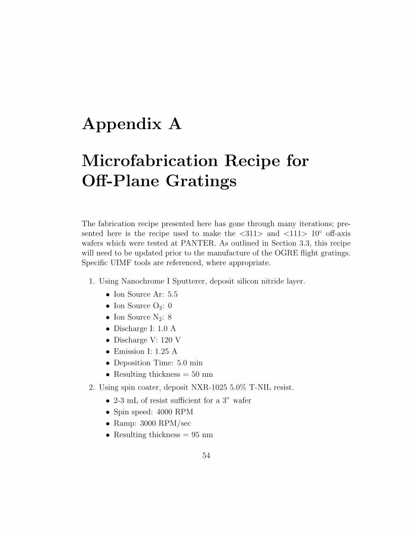
Appendix A
Microfabrication Recipe forOff-Plane Gratings
The fabrication recipe presented here has gone through many iterations; pre-sented here is the recipe used to make the <311> and <111> 10◦ off-axiswafers which were tested at PANTER. As outlined in Section 3.3, this recipewill need to be updated prior to the manufacture of the OGRE flight gratings.Specific UIMF tools are referenced, where appropriate.
1. Using Nanochrome I Sputterer, deposit silicon nitride layer.
• Ion Source Ar: 5.5
• Ion Source O2: 0
• Ion Source N2: 8
• Discharge I: 1.0 A
• Discharge V: 120 V
• Emission I: 1.25 A
• Deposition Time: 5.0 min
• Resulting thickness = 50 nm
2. Using spin coater, deposit NXR-1025 5.0% T-NIL resist.
• 2-3 mL of resist sufficient for a 3” wafer
• Spin speed: 4000 RPM
• Ramp: 3000 RPM/sec
• Resulting thickness = 95 nm
54

3. Soft bake-out of T-NIL resist.
• Temperature: 120◦ C
• Duration: 5 min
4. Using Nanonex NX-1000, imprint grating mold pattern with T-NIL step.
• Clean treated mold with acetone, methanol, and isopropanol rinse,N2 to dry
• Orient grating mold along <110> direction
• Preliminary pressure: 130 psi
• Imprint temperature: 130◦ C
• Imprint pressure: 200 psi
5. Using Oxford NGP-80, RIE T-NIL resist.
• O2: 10.0 sccm
• Ar: 5.0 sccm
• Power: 40 W RF
• Operating pressure: 10 mTorr
• Strike: 70 mTorr
• Process Time: 75 sec
6. Using Oxford NGP-80, RIE silicon nitride layer.
• O2: 10.0 sccm
• CHF3: 50.0 sccm
• Power: 150 W RF
• Operating pressure: 100 mTorr
• Process Time: 38 sec
7. Strip remaining T-NIL via acetone soak.
• Agitation spin: 200 RPM
• Process duration: 5.0 minutes
8. Remove native silicon dioxide via buffered HF dip.
• Solution concentration: 16% ammonium fluoride in H2O
• Acid concentration: 49% HF
• Mix in 20:1 ratio (solution : acid)
• Process duration: 5 sec
9. Etch silicon substrate with KOH.
55

• KOH solution: 20% by weight
• Temperature: 20◦ C
• Process duration: 20 sec
10. Halt etch via H2O soak.
• Agitation spin: 200 RPM
• Process duration: 3.0 min
11. Remove silicon nitride layer via concentrated HF soak.
• Acid concentration: 49% HF
• Process duration: 3.0 min
12. Rinse residual HF from substrate.
• Solution: H2O
• Agitation spin: 200 RPM
• Process duration: 3.0 min
13. Clean substrate of particulate.
• Acetone spray rinse
• Pressurized (80 psi) N2 flow over substrate
56