Use of Niobium for Fabricating Superconducting Radio Frequency Cavities
104
1 Use of Niobium for Fabricating Superconducting Radio Frequency Cavities * A.T. Wu Thomas Jefferson National Accelerator Facility, 12000 Jefferson Avenue, Newport News, VA 23606, USA Abstract: Since the pioneer work done by the High-Energy Physics Lab at Stanford University in 1965, superconducting radio frequency (SRF) technology has been developing steadily up to now. Demanding on niobium (Nb) has been increasing constantly, since more and more particle accelerators select Nb based SRF technology as a key part of their accelerator constructions. For example, the proposed International Linear Collider (ILC) that will probe new physics using TeV collisions of electron and positron beams will need approximately 17,000 1-meter-long Nb SRF cavities. Others such as x-ray free electron laser (XFEL) at DESY in Germany, energy recovery linac (ERL) at Cornell University in USA, the new Spiral 2 facility in France, the isotope separation and acceleration (ISAC) II in Canada, and the 12 GeV upgrade of CEBAF at Jefferson Lab in USA will all require Nb. This popularity in Nb can be, at least partially, attributable to the unique physical and mechanical properties that Nb possesses --- the highest superconducting transition temperature of 9.25 K and the highest superheating field of 0.23 T among all available pure metals with excellent ductility that enables machining to be done relatively easily. In this chapter, the use of Nb for fabricating SRF cavities is reviewed, giving particular attention to some examples of important new developments in the past decade on reducing the production costs and increasing the throughput of high quality Nb SRF cavities. Some R&D examples on the study of the requirements in the physical, chemical, metallurgical, and mechanical properties of Nb for the applications in particle accelerators based on Nb SRF technology are updated and reviewed. This chapter also includes some unpublished experimental results from my own research. Hopefully this review can be served as a useful reference for new researchers who want to use Nb for their various R&D projects in particle accelerators and for Nb suppliers and manufacturers who want to provide the best and the most economic products to be used in particle accelerators.
-
Upload
independent -
Category
Documents
-
view
5 -
download
0
Transcript of Use of Niobium for Fabricating Superconducting Radio Frequency Cavities
1
Use of Niobium for Fabricating Superconducting Radio
Frequency Cavities*
A.T. Wu
Thomas Jefferson National Accelerator Facility, 12000 Jefferson Avenue, Newport
News, VA 23606, USA
Abstract:
Since the pioneer work done by the High-Energy Physics Lab at Stanford University in
1965, superconducting radio frequency (SRF) technology has been developing steadily up to
now. Demanding on niobium (Nb) has been increasing constantly, since more and more particle
accelerators select Nb based SRF technology as a key part of their accelerator constructions. For
example, the proposed International Linear Collider (ILC) that will probe new physics using TeV
collisions of electron and positron beams will need approximately 17,000 1-meter-long Nb SRF
cavities. Others such as x-ray free electron laser (XFEL) at DESY in Germany, energy recovery
linac (ERL) at Cornell University in USA, the new Spiral 2 facility in France, the isotope
separation and acceleration (ISAC) II in Canada, and the 12 GeV upgrade of CEBAF at Jefferson
Lab in USA will all require Nb. This popularity in Nb can be, at least partially, attributable to
the unique physical and mechanical properties that Nb possesses --- the highest superconducting
transition temperature of 9.25 K and the highest superheating field of 0.23 T among all available
pure metals with excellent ductility that enables machining to be done relatively easily. In this
chapter, the use of Nb for fabricating SRF cavities is reviewed, giving particular attention to
some examples of important new developments in the past decade on reducing the production
costs and increasing the throughput of high quality Nb SRF cavities. Some R&D examples on
the study of the requirements in the physical, chemical, metallurgical, and mechanical properties
of Nb for the applications in particle accelerators based on Nb SRF technology are updated and
reviewed. This chapter also includes some unpublished experimental results from my own
research. Hopefully this review can be served as a useful reference for new researchers who
want to use Nb for their various R&D projects in particle accelerators and for Nb suppliers and
manufacturers who want to provide the best and the most economic products to be used in
particle accelerators.
2
1. Introduction
The use of SRF technology in particle accelerators was started by the pioneer work done
at Stanford University in 1965 where electrons were accelerated in a lead-plated resonator1.
Since then, Nb has been gradually taking over as the main metal for fabrication SRF resonators
or cavities due to its unique physical and mechanical properties. Although the major
consumption of Nb is as an alloying element to strengthen high-strength-low-alloy steels for
building automobiles and high pressure gas transmission pipelines and to provide creep strength
in superalloys operating in the hot section of aircraft gas turbine engines, demands on Nb from
SRF community have been increasing steadily over the last couple of decades due to the fact that
many current and future particle accelerators select Nb based SRF technology as one of the key
parts in their accelerator constructions for the applications in nuclear physics, high energy
physics, and free electron laser. Some examples of large scale particle accelerators that utilize
Nb based SRF technology include CEBAF2, KEKB
3, RIA
4, TESLA
5, SNS
6, SPIRAL2
7,
ISAC28, XFEL
9, and ILC
10 etc. For instance, the proposed International Linear Collider (ILC)
alone will require roughly 520 tons of Nb by assuming a production yield of 80% and a thickness
of 3 mm for the Nb sheets. This is quite significant since the total production of Nb in the world
in 2008 is only 60000 tons11
.
As the popularity in Nb-based SRF technology grows, more and more people are
involved in the R&D of the technology. One example of the growing in this field is the
evolution of the previous SRF workshop to SRF conference in 2009 due to the increasing
numbers of participants and contributed papers. For instance, the number of the contributed
papers has grown from 127 for the SRF workshop in 2001 to 223 for the SRF conference in
2009. This is an increase of more than 75%. More and more consensuses have been reached
regarding what the requirements are on Nb for the applications in the SRF field. In this chapter,
I will try to update and review some selected aspects of the developments in cavity fabrication
process and some R&D examples on the requirements in physical, chemical, metallurgical, and
mechanical properties of Nb for fabricating Nb SRF cavities. It represents only my personal
interests and viewpoints and it is by no means the complete coverage of the entire R&D activities
in this field.
This chapter will be organized in the following way: Section 1 gives a brief introduction
to the several important fundamental parameters employed in SRF technology. This defines the
3
terminology that we will use in this chapter. The benefits for selecting Nb as the material for
SRF applications are discussed in Section 2. Section 3 summarized the steps in fabricating Nb
SRF cavities with emphases on some newly emerged techniques in the fabrication process
aiming at reducing the production costs and increasing the throughput of high quality Nb SRF
cavities. Some examples of R&D on exploring the requirements in physical, chemical,
metallurgical, and mechanical properties of Nb are shown and discussed in Section 4. Section 5
presents a summary and a very brief perspective in the application of Nb for fabricating SRF
cavities.
Section 1: Some Fundamental Parameters Employed in SRF
Technology
There are two different groups of particle accelerating structures commonly used for
particle accelerators, depending on the velocity (V) of the particle to be accelerated. Normally, a
parameter β that is defined as V/C where C is the velocity of light is used to separate the two
groups.
When 0.5< β <1, this is typical for accelerating electrons with kinetic energy of a few
MeV and protons with 100 MeV. A typical Nb SRF cavity for this group of particle accelerating
structures is shown in Fig.1 where a chain of five coupled RF cells are resonating in the
transverse magnet (TM010) mode. This accelerating structure is the topic of the discussions for
this chapter. In this field configuration, the longitudinal electric field is maximized along the
axis of the cavity and the RF phase between adjacent cells is 180 o as schematically illustrated in
the upper part of Fig.1. In this way, a particle with velocity close to the speed of light will
experience the maximum acceleration in each cell of the cavity.
When β < 0.5, this is the typical for accelerating ions from helium to uranium with
kinetic energies from a few to 20 MeV per nucleon. For this group, a variety of different
accelerating structures may exist such as, for instance, coils, helix, spoke, and crab shapes tec.
Fig.2 shows an example of how the cavities look like from this cavity group. Based on the past
experience, we know that the major consumption of Nb is from the first group of accelerators
where 0.5< β <1.
Normally, the performance of a SRF cavity is characterized by an excitation curve where
the quality factor Qo is plotted as a function of the accelerating gradient Eacc. Therefore, we need

4
to define first several fundamental parameters used often in SRF technology including the
quality factor Qo, the accelerating gradient Eacc, the surface resistance Rs, and the RRR value.
1.1 Quality Factor Qo
The quality factor Qo of a cavity is defined as the ratio of stored energy (U) in the cavity
to the dissipated power (P) through the cavity walls per radian per second
Qo=ω (U/P) (1)
Where ω=2πf. f is the frequency of the stored RF power. Qo is inversely proportional to
the Rs of the wall material
Qo=G/Rs (2)
Where G is called the geometry constant. Here it is assumed that the surface resistance
of the wall material is homogenous over the whole interior surface of the cavity.
P can also be expressed in the following way:
P=
Rs ׀ ׀
2 ds (3)
Where H is the local magnetic field and the integral is taken over the entire interior cavity
surface.
1.2 Accelerating Gradient Eacc
The accelerating gradient Eacc is defined as the maximum energy gain for a charged
particle when traveling through a cavity divided by the length of the cavity and the charge of the
particle. It is can be expressed as
Eacc (4)
5
1.3 Surface Resistance Rs
Surface resistance Rs of the wall material of a SRF cavity is related to the power
dissipation P through equation 3. For a superconductor such as Nb at a temperature below the
superconducting transition temperature (Tc), Rs can be expressed as
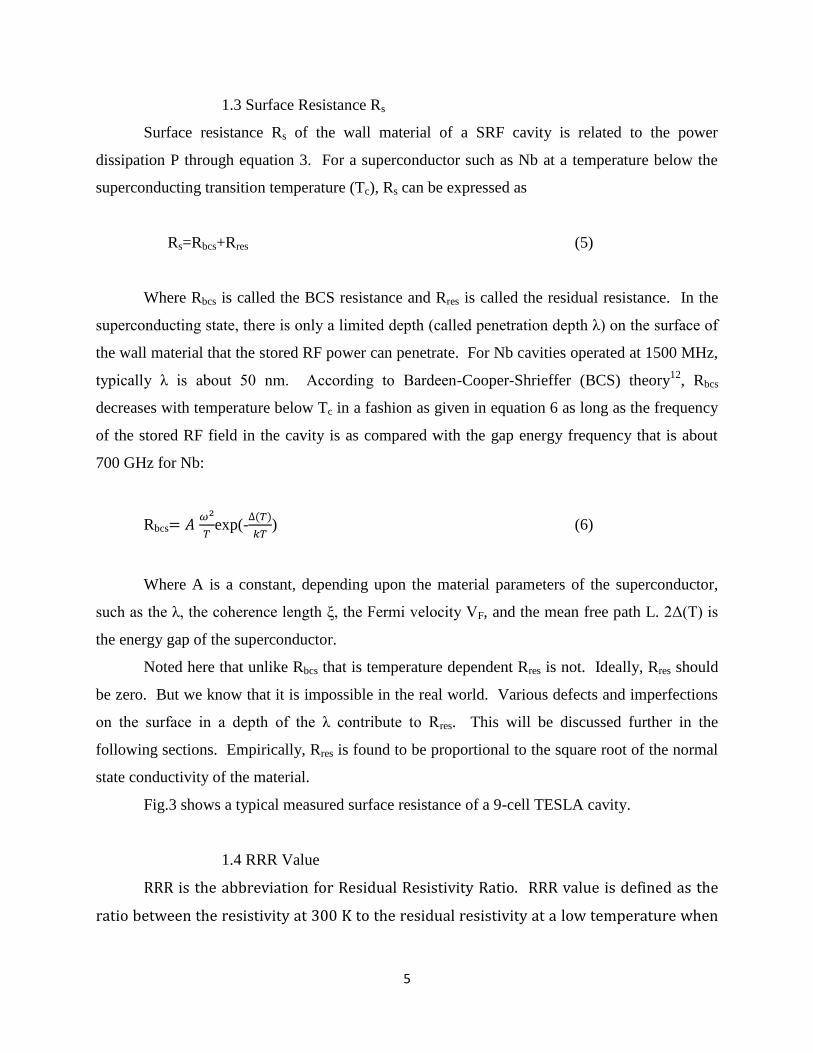
Rs=Rbcs+Rres (5)
Where Rbcs is called the BCS resistance and Rres is called the residual resistance. In the
superconducting state, there is only a limited depth (called penetration depth λ) on the surface of
the wall material that the stored RF power can penetrate. For Nb cavities operated at 1500 MHz,
typically λ is about 50 nm. According to Bardeen-Cooper-Shrieffer (BCS) theory12
, Rbcs
decreases with temperature below Tc in a fashion as given in equation 6 as long as the frequency
of the stored RF field in the cavity is as compared with the gap energy frequency that is about
700 GHz for Nb:
Rbcs
exp(-
) (6)
Where A is a constant, depending upon the material parameters of the superconductor,
such as the λ, the coherence length ξ, the Fermi velocity VF, and the mean free path L. 2Δ(T) is
the energy gap of the superconductor.
Noted here that unlike Rbcs that is temperature dependent Rres is not. Ideally, Rres should
be zero. But we know that it is impossible in the real world. Various defects and imperfections
on the surface in a depth of the λ contribute to Rres. This will be discussed further in the
following sections. Empirically, Rres is found to be proportional to the square root of the normal
state conductivity of the material.
Fig.3 shows a typical measured surface resistance of a 9-cell TESLA cavity.
1.4 RRR Value
RRR is the abbreviation for Residual Resistivity Ratio. RRR value is defined as the
ratio between the resistivity at 300 K to the residual resistivity at a low temperature when
6
the material under the measurement is in normal state. It can be expressed mathematically
as:
RRR=
(7)
For Nb, this is usually done either by the measurement at a temperature just before
the superconducting transition temperature Tc and extrapolation to 4.2 K or at a specific
temperature below Tc where an external magnetic field is applied just enough (a
homogeneous magnetic field up to 1 Tesla parallel to sample) to drive Nb to lose its
superconductivity at 4.2 K.
RRR is a parameter that can be used to quantify the general impurity content of a
material. The higher is the RRR, the lower is the impurity content of the material. It is
important to point out here that there are background contributions to RRR value from
phonons and grain boundaries. Calculated theoretical limit13 for RRR for Nb is 35000. In
practice, the highest RRR ever achieved14 for Nb is 33000.
Generally speaking, a good Nb cavity should have Eacc>35 MV/m and Qo > 1010.
This would imply that the surface resistance sh uld be less than a few tens f nΩ. RRR
value is larger than 300.
Section 2: Why Is Nb The Material of Choice
To answer this question, first we have to answer why the cavities have to be
superconducting. For any particle accelerators, the operation cost is one of the most important
factors that require careful consideration before construction. Selection of superconducting
cavities over normal conducting cavities as the accelerating structure of an accelerator can result
in huge savings in the operation cost. This is especially true for accelerators in a continuous
wave (cw) mode or at a high duty factor (>1%).
Take copper (Cu) cavities as an example. For cw operation, the power dissipation
through the walls of a Cu cavity is huge. This is due to the fact that the dissipated power per unit
length of an accelerating structure is given by the following formula:
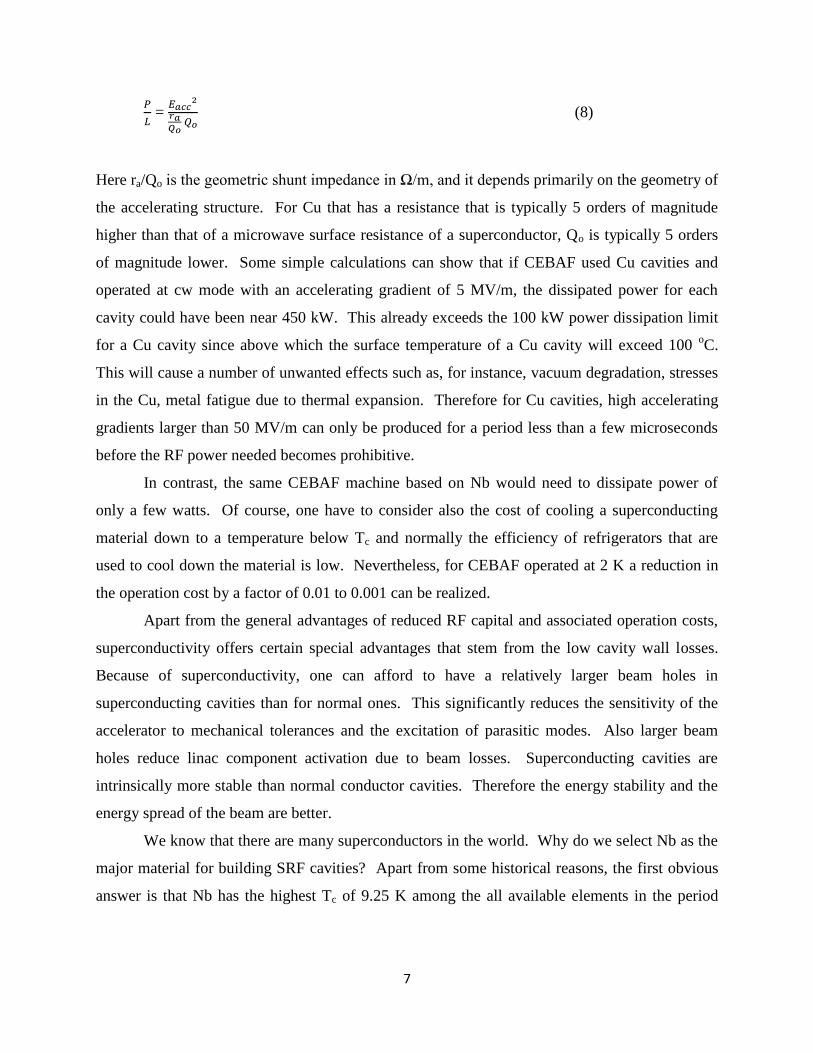
7
=
(8)
Here ra/Qo is the geometric shunt impedance in Ω/m, and it depends primarily on the geometry of
the accelerating structure. For Cu that has a resistance that is typically 5 orders of magnitude
higher than that of a microwave surface resistance of a superconductor, Qo is typically 5 orders
of magnitude lower. Some simple calculations can show that if CEBAF used Cu cavities and
operated at cw mode with an accelerating gradient of 5 MV/m, the dissipated power for each
cavity could have been near 450 kW. This already exceeds the 100 kW power dissipation limit
for a Cu cavity since above which the surface temperature of a Cu cavity will exceed 100 oC.
This will cause a number of unwanted effects such as, for instance, vacuum degradation, stresses
in the Cu, metal fatigue due to thermal expansion. Therefore for Cu cavities, high accelerating
gradients larger than 50 MV/m can only be produced for a period less than a few microseconds
before the RF power needed becomes prohibitive.
In contrast, the same CEBAF machine based on Nb would need to dissipate power of
only a few watts. Of course, one have to consider also the cost of cooling a superconducting
material down to a temperature below Tc and normally the efficiency of refrigerators that are
used to cool down the material is low. Nevertheless, for CEBAF operated at 2 K a reduction in
the operation cost by a factor of 0.01 to 0.001 can be realized.
Apart from the general advantages of reduced RF capital and associated operation costs,
superconductivity offers certain special advantages that stem from the low cavity wall losses.
Because of superconductivity, one can afford to have a relatively larger beam holes in
superconducting cavities than for normal ones. This significantly reduces the sensitivity of the
accelerator to mechanical tolerances and the excitation of parasitic modes. Also larger beam
holes reduce linac component activation due to beam losses. Superconducting cavities are
intrinsically more stable than normal conductor cavities. Therefore the energy stability and the
energy spread of the beam are better.
We know that there are many superconductors in the world. Why do we select Nb as the
major material for building SRF cavities? Apart from some historical reasons, the first obvious
answer is that Nb has the highest Tc of 9.25 K among the all available elements in the period
8
table. This makes the requirement for cooling the cavities down to a temperature below Tc a
relatively easy task.
Furthermore, since Eacc is proportional to the peak electric field (Epk) and peak magnetic
field (Hpk) on the surface of a cavity, one has to be sure that the material that is used to make the
cavity can sustain large surface fields before causing significant increase in surface resistance or
a catastrophic breakdown of superconductivity (called quench). The ultimate limit to
accelerating gradient is the theoretical RF critical magnetic field that is called the superheating
field Hsh. Nb has the highest Hsh of 0.23 T among the all available metal elements.
Another advantage of Nb is that it is relatively easy to be shaped into different structures
due to its outstanding ductility and the fact that it is relatively soft (see Table 1). Nb can be cold-
worked to a degree more than 90% before annealing becomes necessary. This property is
responsible for the recent new developments on fabricating seamless Nb SRF cavities by
hydroforming and spinning as described in the following section.
Although there are other superconducting compounds that have higher Tc or higher Hsh,
they either are not having the three mentioned characters in a superconductor or were discovered
much later as superconductors than Nb. It is fair to say that so far Nb is the most investigated
material for SRF applications and the major material used in particle accelerators based on SRF
technology.
Only limited research effort has been put on other superconductors such as NbN (Tc=16.2
K), NbTiN (Tc=17.5 K), Nb3Sn (Tc=18.3 K), V3Si (Tc=17 K), Mo3Re (Tc=15 K), and MgB2
(Tc=39 K). Interested readers for this topic are referred to an overview paper15
from Valente-
Feliciano.
It is worth mentioning that recently some groups16
have started to revisit the Nb on Cu as
an alternative for making SRF cavities by taking the advantages of the good superconducting
properties of Nb and good thermal conductivity and cheap Cu substrates.
I am not going to discuss high temperature superconductors such as, for instance, MgB2,
YBCO, BICCO, etc here since they are not related to Nb that is the topic of this book.
Section 3: Fabrication of Nb Cavities
In order to understand and improve the use of Nb in fabricating Nb SRF cavities, we have
to know the typical procedure for doing it. Fig.4 shows a flow chart for a typical procedure of
9
Nb cavity fabrication. This procedure has been well established in the past couple of decades
and does not various much from one lab to another. However, significant amount of new
developments have taken place in the last decade or so on how each step is done in reality. For
instance, Step 15 in Fig.4 can be done in many ways, including Buffered Chemical Polishing
(BCP), ElectroPolishing (EP), barrel polishing, or Buffered ElectroPolishing (BEP). In this
section, I will first give a general description of the fabrication steps with emphasis on some
selected examples of new developments at some steps of the typical cavity fabrication process.
3.1: Typical Fabrication Steps for a Nb SRF Cavity
Normally the as-received Nb sheets from suppliers are either 3 or 4 mm thick. To
prevent them from damages and contaminations during transportation, the Nb sheets are covered
by sticking tapes that can be peered off. The first thing to do after receiving Nb sheets is to
check whether they meet the material specifications. The specifications typically cover RRR
value, grain size, impurity tolerance, surface finish, yield strength, and flatness. The sheets are
then either deep drawn or spun to form half cells. Trimming is then done to the half cells to
remove any irregularities and undesirable features. Normally a lathe or a computer controlled
milling machine is employed for the trimming. Since trimming may introduce some
contaminants on the surfaces of the half cells, degreasing is then needed. Degreasing normally
takes place in soap and water in an ultrasonic tank and then a light BCP of 5 µm is done to the
further remove any undesirable residuals on the surfaces of the half cells from the previous
fabrication or handling steps. After cleaning and visual inspection for surface scratches, defects,
and rust, electron beam (E-beam) welding on iris can then be performed. It is a good practice to
do some grinding on the welded region to make sure that inner surfaces are smooth. Then a light
BCP of 5 µm is done again before E-beam welding on equator takes place. Note here that all
welding should be done in vacuum at a pressure less than 10-5
to avoid significant impurity
intake during these steps. After these steps, we obtain Nb cavities. The cavities are then
chemically polished again for about 100 µm in order to make sure that it is completely clean.
Then cavities are normally baked at a temperature between 1350 to 1400 oC in a titanium
enclosure in a high vacuum furnace for a few hours to purify the cavities. Titanium is a good
getter for oxygen, nitrogen, and other gases. This process also serves as an annealing process to
remove some of the defects such as edge or screw dislocations generated during the previous
10
fabrication steps, especially from depth drawing and spinning. Then the final and the most
important surface Nb removal of 150 µm is followed. This step removes the mechanically
damaged layer as well as any evaporated niobium scale deposited on the surface during welding.
Then tuning to the correct frequency and field flatness is needed, since a thickness of 260 µm of
Nb has been removed the inner surface of a Nb cavity. At this stage, additional 5 µm Nb can be
removed from the inner surface of the cavity, but is not necessary. Final rinsing and cleaning are
then performed before assembling end flanges and couplers in a clean room. Finally the cavity is
pumped down and then baked at 120 oC for 48 hours before RF test.
3.2: Examples of Innovative Techniques for Fabricating Nb SRF Cavities
Recently, Nb SRF cavities have been also fabricated by hydroforming17
and spinning18
to
create seamless cavities.
Fig.5 shows the principle of hydroforming technique. This technique starts with Nb tubes
with a diameter half way between the iris and equator. The diameter at iris has to be reduced
while the diameter at equator has to be expanded. Since the ratio of the diameters between
equator and iris for a typical elliptical cavity is ~3, any attempt to form seamless cavities from
tubes is a significant challenge. Once has to balance the hardness and roughness introduced by
the diameter expansion at equator and the diameter reduction at iris to the inner surface of a
seamless cavity. It was found17
that a starting tube diameter between 130 and 150 mm is optimal
for a 1.3 GHz cavity. This technique can be used to produce single cell and multi-cell cavities.
The very first Nb double cell cavity produced by hydroforming is shown in Fig.6. The highest
Eacc for a single cell seamless cavity reaches 43 MV/m as shown in Fig.7.
It was demonstrated18
by Palmieri that single cell and multi-cell Nb and Cu seamless
cavities could also be fabricated by spinning. Fig.8 shows the progressive steps during the
fabrication of a single cell seamless Cu cavity by this technique. After spinning, cavity has to be
tumbled and mechanically ground for at least 100 µm to remove surface fissures before any
further chemical treatment. Typical excitation curves at 1.6 K for a spun seamless single cell Nb
cavity are shown in Fig.9. Several single cell cavities reach an accelerating gradient of 40 MV/m
with a decent Qo. Fig.10 shows the first nine-cell Nb cavity manufactured by the spinning
technique. Unfortunately the cavity was damaged before a RF measurement was done. One
challenge for this technique is that cavities can be quite thin after fabrication.
11
Although there are still many technical problems waiting to be resolved for the seamless
cavity formation techniques, the exclusion of welding steps from cavity fabrication process is a
very significant progress. These new developments also alter the flow chat shown in Fig.4.
Another interesting idea for fabricating Nb SRF cavities is that after Step 9 in Fig.4 Step
15 is followed. Then the polished Nb dumbbells are E-beam welded to form muilti-cell cavities.
Followed either by a light BCP removal of 5 µm + high pressure water rinse (HPWR) or just
simply HPWR before being evacuated for RF tests. The attractiveness of this idea is that the
final chemical treatment on multi-cell cavities can be avoided, which makes the life in this SRF
world much simpler and easier. This can be very important for electropolishing if it is employed
as the final chemical treatment, since I personally believe strongly19
that the cathode shape
matters during electropolishing on Nb. The size of a cathode is limited by the size of the beam
tube of a cavity if electropolishing has to be done on the cavity. This development is on-going
through acollaboration between Peking University (PKU) and JLab. Nb dumbbells will be
polished by BEP at PUK employing a shaped aluminum cathode fabricated at JLab (see Fig.11).
The thus formed cavities will be treated by HPWR and then RF-tested at JLab. It has been
demonstrated20
by PKU that bright and shining Nb dumbbells can be fabricated by BEP via a
shaped Al cathode as shown in Fig.12.
3.3: Examples of New Developments in Inspection Technique
In my view, there are several key steps in cavity fabrication process that deserve strong
attention to ensure the outcome of good cavities with decent excitation curves. The first of such
key steps is to make sure that the as-received Nb sheets meet the specifications.
3.3.1: Eddy Current and SQUID Scanning
One significant new development in this respect is the application of eddy current and
Superconducting QUantum Interference Device (SQUID) scanning21,22
to check the defects on
the as-received Nb sheets. This allows the removal of some defective starting materials before
going into cavity fabrication.
Eddy current scanning is a nondestructive technique. The working principle of this
technique is schematically shown in Fig.13. A double-coil sensing probe is used to detect
inclusions and defects embedded under the surface by detecting the alternation of the eddy
12
currents. It is important to keep the distance between sensing head and the sample constant
during scanning. Typically it takes about 15 minutes to scan a sample size of 300X300 mm2 and
a line width of 1 mm. Defects deeper than 0.1 mm from the surface are typically undetectable.
This can be improved by replacing the double-coil sensing probe by a SQUID detector. The
working principle of the SQUID scanning technique is shown in Fig.14 where the SQUID is
used to detect the secondary magnetic field of the eddy current. Probing depth can be improved
up to 2.8 mm for a SQUID scanning device operated at 90 kHz with an excellent signal noise
ratio. Latest developments on eddy current scanning can also be found at Reference 25.
3.3.2: Kyoto Camera
Checking whether the welding is done satisfactorily and how the welding area and areas
close to the welding area look like especially on the inner surface of a cavity are also very critical
during cavity fabrication. In the past, this was usually done by a borescope, long distance
microscope, or a well-lit angle mirror. All of these were inaccurate and not quantitative. It can
become quite a challenge to apply the devices to a multi-cell cavity. Recently a new camera
based system26
was developed jointly by Kyoto University and KEK, which can be used to
examine the inner surface quality even for a 9 cell cavity. The schematic diagram of this so
called “Kyoto Camera” is shown in Fig15a and the associated key components are shown in
Fig.15b. During inspection, the cavity is rotated and moved while the cylinder is kept stationary.
The inner surface of the cavity is reflected by the mirror and the image is captured by the
camera. A real setup of this system is shown in Fig.16. The resolution of Kyoto Camera can
reach 7.5 µm per pixel.
By dividing the electro-luminescence sheets into strips to form a strip illuminator and by
turning on and off each illumination strip and then following the movement of the bright point
across a defect, it is possible to obtain quantitative information regarding the defect structure on
the surface via simple geometric consideration. A typical example of this is shown in Fig.17.
Further information about Kyoto Camera and examples of real observations can be found also in
Refs 25 and 27.
3.3.3: Replica Technique
13
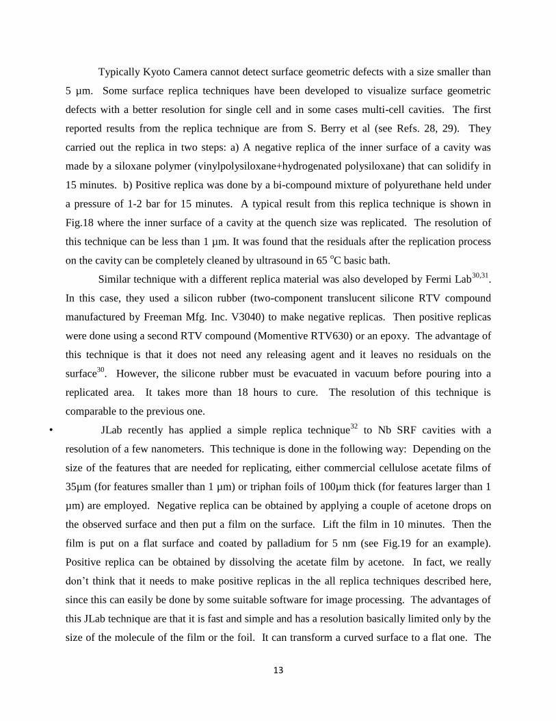
Typically Kyoto Camera cannot detect surface geometric defects with a size smaller than
5 µm. Some surface replica techniques have been developed to visualize surface geometric
defects with a better resolution for single cell and in some cases multi-cell cavities. The first
reported results from the replica technique are from S. Berry et al (see Refs. 28, 29). They
carried out the replica in two steps: a) A negative replica of the inner surface of a cavity was
made by a siloxane polymer (vinylpolysiloxane+hydrogenated polysiloxane) that can solidify in
15 minutes. b) Positive replica was done by a bi-compound mixture of polyurethane held under
a pressure of 1-2 bar for 15 minutes. A typical result from this replica technique is shown in
Fig.18 where the inner surface of a cavity at the quench size was replicated. The resolution of
this technique can be less than 1 µm. It was found that the residuals after the replication process
on the cavity can be completely cleaned by ultrasound in 65 oC basic bath.
Similar technique with a different replica material was also developed by Fermi Lab30,31
.
In this case, they used a silicon rubber (two-component translucent silicone RTV compound
manufactured by Freeman Mfg. Inc. V3040) to make negative replicas. Then positive replicas
were done using a second RTV compound (Momentive RTV630) or an epoxy. The advantage of
this technique is that it does not need any releasing agent and it leaves no residuals on the
surface30
. However, the silicone rubber must be evacuated in vacuum before pouring into a
replicated area. It takes more than 18 hours to cure. The resolution of this technique is
comparable to the previous one.
• JLab recently has applied a simple replica technique32
to Nb SRF cavities with a
resolution of a few nanometers. This technique is done in the following way: Depending on the
size of the features that are needed for replicating, either commercial cellulose acetate films of
35µm (for features smaller than 1 µm) or triphan foils of 100µm thick (for features larger than 1
µm) are employed. Negative replica can be obtained by applying a couple of acetone drops on
the observed surface and then put a film on the surface. Lift the film in 10 minutes. Then the
film is put on a flat surface and coated by palladium for 5 nm (see Fig.19 for an example).
Positive replica can be obtained by dissolving the acetate film by acetone. In fact, we really
don’t think that it needs to make positive replicas in the all replica techniques described here,
since this can easily be done by some suitable software for image processing. The advantages of
this JLab technique are that it is fast and simple and has a resolution basically limited only by the
size of the molecule of the film or the foil. It can transform a curved surface to a flat one. The
14
latter point can be extremely useful for subsequent observations or measurements since some
instruments (for instance an optical microscope) are very difficult to be applied to a curved
surface. The replicas can be examined not only by an optical microscope and a profilometer, but
also by a scanning electron microscope (SEM) or a transmission electron microscope (TEM).
One challenge for the above mentioned replica techniques is how to effectively apply
them to multi-cell cavities when hands are not long enough.
3.4: Examples of New Developments in Final Chemical Treatment
Step 15 in the Fig.4 is perhaps the most critical one in determining the performance of a
Nb SRF cavity. It is normally done by either BCP employing the acid mixture of phosphoric,
hydrofluoric, and nitric acids with a ratio of 1:1:1 or 2:1:1 or by EP employing the acid mixture33
of hydrofluoric and sulfuric acids. There are quite some new developments on this topic in the
last decade. Most of them are done along the line of modifying or improving the existing
techniques. Due to the limited space, here I will discuss only a few new developments that have
shown some promising signs. One34
is BEP. Others include: a) Nb polished35
by ionic liquids at
a temperature higher than 100 oC, b) Plasma Etching
36, and c) FARADAYIC Electropolishing
37.
3.4.1: Buffered Electropolishing (BEP)
BEP experiment was initiated at JLab in early 2001. Some preliminary results were
published in Ref. 38. BEP uses the acid mixture of hydrofluoric, sulfuric, and lactic acids as the
electrolyte at a volume ratio of 4:5:11. Here lactic acid acts as a buffer in a similar way as what
H3PO4 does in BCP. By replacing the majority of H2SO4 in the conventional EP, BEP treatment
reduces the aggressiveness of the electrolyte significantly. It has been demonstrated that BEP
can produce the smoothest39-42
Nb surface ever reported in the literature. Smoother inner surface
of a Nb SRF cavity is known to have positive effects on its RF performance. Experiments also
show39,43 that Nb removal rate can be as high as 4.66μm/min. This is more than 10 times faster
than 0.38 μm/min of EP. Faster Nb removal rate can contribute significantly to the reduction of
the capital costs of the surface treatments for Step 15. For instance, conventional EP will take
typically 23622 seconds to get Step 15 done. With BEP, it takes only 1931 seconds. Other
benefits of BEP as compared with EP include: a) acid mixture is much safer to handle, b) the life
of the acid mixture is longer, c) acid mixture is cheaper, and d) less or no sulfur precipitation.
15
CH3
O
O-
O-
CH3
O
O-
O-
Fig.20 shows a quantitative comparison on the surface smoothness for Nb treated by BEP, EP,
and BCP as measured by a precision 3-D profilometer34
. The RMS of the smoothest Nb
surface39
treated by BEP is 20 nm over an area of 200X200 µm2. To the best of my knowledge,
this is also the smoothest Nb surface ever reported in the literature.
Early experiments38
done on Nb half cells have implied that cathode shape plays an
important role during BEP treatments on curved surfaces. This is confirmed later by
experiments at other labs20,42,44
. Fig.21 shows a typical example of the surface finish for a Nb
half cell treated by BEP for 1800 seconds without electrolyte circulation when the shape of the
cathode is changed in such a way to allow a more homogenous electric field distribution inside
the half cell.
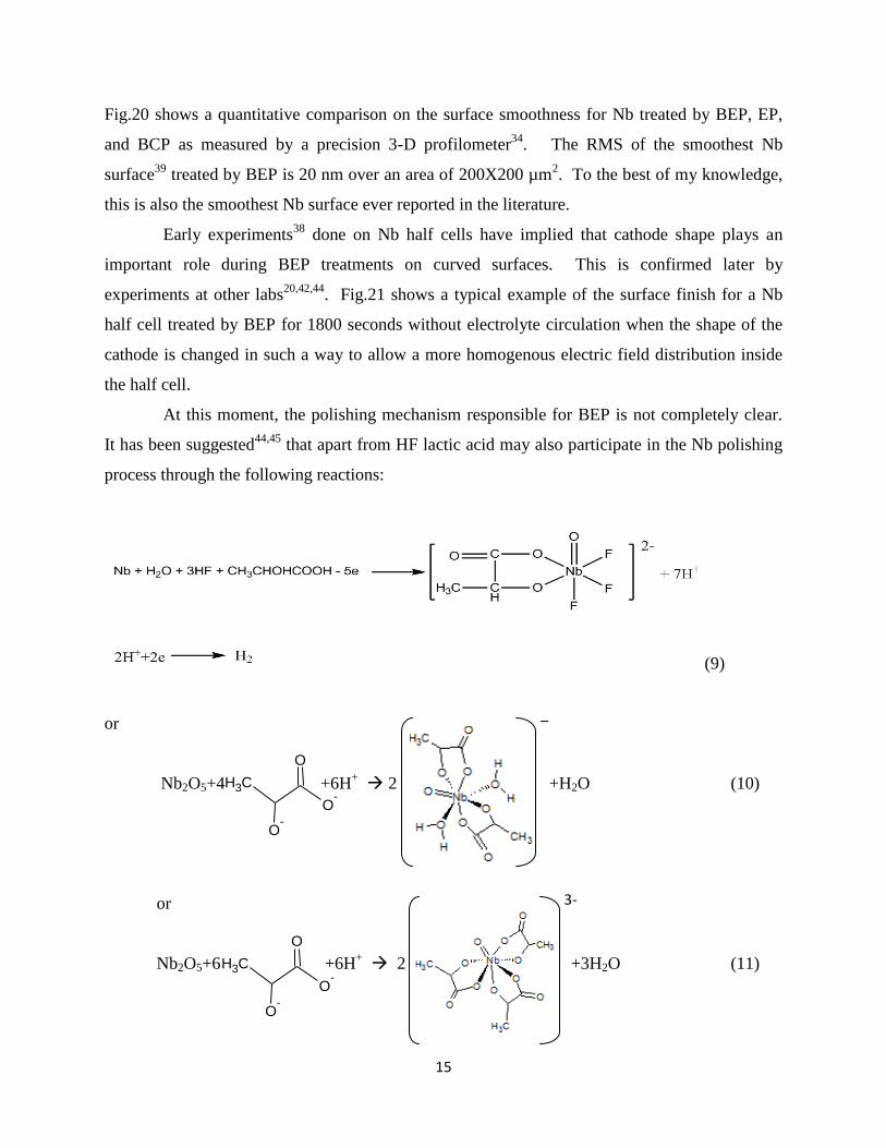
At this moment, the polishing mechanism responsible for BEP is not completely clear.
It has been suggested44,45
that apart from HF lactic acid may also participate in the Nb polishing
process through the following reactions:
(9)
or
Nb2O5+4 +6H+ 2 +H2O (10)
or
Nb2O5+6 +6H+ 2 +3H2O (11)
3-
_
16
This may explain why BEP can polish at a much faster way than conventional EP.
To investigate whether BEP was governed by diffusion of fluorine ions, experiments42
with a rotating disc electrode were carried out at CEA Saclay in France. The result is duplicated
in Fig.22. where polishing current (I) was found to be not proportional to the square root of the
angular speed (ωa) of the rotation disc, implying that the diffusion is not the only process taking
place during BEP. If the polishing is diffusion limited, I is related to ωa in the following way46
:
I=6.2x10⁻⁴
nFSD2/3
ν-1/6
ωa1/2
C (12)
Where n is the number of electrons in the electrochemical reaction; S is the surface of the
electrode (cm2); D is the diffusion coefficient (cm
2/s); ν is the viscosity (St); C is the
concentration of the active species (mol/l).
Further measurements42
with Electrochemical Impedance Spectroscope (EIS) seemed to
indicate the polished surface might be covered by a porous film whose resistance increased with
the applied potential.
BEP has been applied to treat Nb SRF single cells both vertically in JLab and
horizontally at CEA Saclay for comparison. In fact, the first very vertical electropolishing on a
Nb SRF cavity was carried out at JLab via BEP in early 2002 as reported in Ref.47. Since then
many improvements48
have been made to the system, including a more reliable acid circulation,
more accurate acid flow control, more efficient heat removal from the treated cavity, external
cooling, and an automatic data acquisition system. The modern system is shown in Fig.23.
The major advantages of vertical EP as compared with the horizontal one are: 1) Easier
for draining. 2) Easier for making the electrode contacts, since cavity rotation is not necessary in
vertical EP. 3) Easier to incorporate other cavity treatment techniques into a vertical setup such
as, for instance, HPWR, BCP, BEP, drying, baking, etc. Of course hydrogen removal is more
difficult for a vertical system, which is especially true for treatments on multi-cell cavities.
So far the best results were all obtained with the vertical system at JLab and shaped
cathodes. Typical excitation curves49
for a CEBAF shape regular grain single cell cavity are
shown in Fig.24. It is noted from Fig.24 that Qo is improved significantly after baking at 120 oC.
The best result was achieved on large grain cavity where Eacc reached 32 MV/m. It is worth
17
pointing out here that the post cleaning procedure for all BEP treated cavities is identical to that
used for conventional EP. Improving on the post BEP cleaning may be one of the keys to open
the door for a better performance for BEP treated Nb cavities. Optimization process on BEP is
now underway.
3.4.2: Other New Developments to Remove Nb
Currently, Step 15 in Fig.4 is normally done with an acid mixture involving HF. HF is
well-known to be very nasty in terms of its effects on the health of human beings. A non-HF
electrolyte for polishing on Nb is a very attractive idea. There are many HF-free recipes for
polishing Nb as listed in Ref.35. Many of them are even most toxic or dangerous than HF is35
.
Two different ionic liquids have been explored to electropolish Nb at temperatures higher than
100 oC at University of Padua. One
35 consists of choline chloride and urea at a ratio of 4:1 plus
sulphamic acid in a concentration of 30 g/l. The other50
is a mixture of urea and choline chloride
at a ratio of 3:1 plus ammonium chloride in a concentration of 10 g/l. Polishing has to take place
at 120 oC and 190
oC respectively
35,50. The highest Nb removal rate can be 12 times quicker than
that of the conventional EP. A typical Nb surface produced by this technique is shown in Fig.25.
Plasma etching on Nb is a R&D project through the collaboration51
between University
of Old Dominion and JLab. The idea here is to use some reactive gas species36,51
such as, for
instance, Ar/Cl2 or BF3 to chemically react with Nb under the discharge from a DC or RF source.
This will generate some volatile Nb compounds that can be pumped away. An experimental
setup employing microwave glow discharge is schematically shown in Fig.26. It was
demonstrated36
that an etching rate of 1.5 µm/min can be reached when Cl2 was used as the
reactive agent. The surface finish produced by plasma etching appears to be comparable to that
by BCP at the present stage of development. This technique is attractive since it does not
employ HF and it can produce a decent etching rate.
Faradayic Electropolishing was developed37
by Faraday Technology Inc. The novelty
here is that instead of using the chemical mediated method to remove oxides from Nb surfaces,
Faradayic Electropolishing employs electrically mediated approach to perform this removal. The
electrolyte they used52
is 20% H2SO4 solution. Here sulfuric acid acts as an oxidation agent.
The key here is that the applied electric field is not constant. It is pulsed and modulated in a way
18
to optimize the polishing. For instance, during Faradayic Electriopolishing chemical reactions
can take place in the following way:
2Nb+5H2O Nb2O5+5H2 (13)
Nb2O5+10H++10e
- 2Nb+5H2O (14)
Reaction formula 13 is the same as that of EP and BEP. However, now by controlling
the electric potential applied to the surface, before the oxide is formed completely as an
insulating layer on the naked Nb surfaces the applied electric field can be either reduced or shut
off to allow newly formed oxides (for instance the pent-oxides) to diffuse away from the
polished surface. After the oxide concentration is returned to its original value, the electric field
will be turned on or ramped up. A typical setup is schematically shown in Fig.27. This
technique can produce a polishing rate as high as 5 µm/min. A typical Nb surface treated by
Faradayic Electropolishing is shown in Fig.28 at a polishing rate of 2.7 µm/min.
It is worth pointing out that any new development is not as simple as it appears to be.
Take BEP as an example, by adding only one additional acid into the electrolyte of the
conventional EP a new whole set of problems emerge. It takes more than 8 years to reach the
stage that it is now. Although the cause of this can always be attributed to external and
environmental factors including lack of manpower and the smartness of the persons involved in
the R&D (easy target), there are perhaps intrinsic reasons due to the nature of any new
development. For instance, how many years does it take to develop the conventional EP? We
are still trying up to now to improve it and to understand the mechanism responsible for it19
.
Therefore one has to be extremely careful before taking on a new development, especially on
something that is completely new.
3.5: Examples of New Developments in Final Cleaning Technique
HPWR with ultra pure water is the process that is normally done in between Steps 17 and
18 as the final cleaning before the assembly and low temperature baking. This final cleaning is
critical since it determines whether there are still contaminants or chemical residuals on the inner
surface of a Nb cavity. These contaminants or chemical residuals can have detrimental effects
19
on cavity performance. Here I will focus on two examples of these new developments. One is
Gas Cluster Ion Beam (GCIB) technique53
. The other is Dry Ice Cleaning (DIC) technique54
.
3.5.1: GCIB Technique
In contrast to HPWR where a mechanical effect is the main cleaning means, as should see
in the following GCIB offers both mechanical and chemical effects in the cleaning. The
application of GCIB technique to Cu RF cavities and Nb SRF cavities was first done55,56
by
Swenson et al at Epion Corporation to mitigate high voltage breakdown through reducing the
surface roughness of oxygen-free Cu via GCIB. Later on, collaboration was established between
Epion Corporation, JLab, Fermi National Accelerator Lab, and Argonne National Lab on a R&D
project to investigate the application of GCIB technique to Nb SRF cavity both experimentally
and theoretically. The results of this collaboration and the current status of the application of this
technique to the treatments of Nb SRF cavities are summarized in Ref.53.
The working principal of GCIB is schematically illustrated in Fig.29. Various types of
gases can be used for GCIB treatments. The gases can be inert such as Ar, Kr, Xe etc. or
chemically reactive such as O2, N2, CO2, NF3, CH4, B2H6 etc. that may react with the surfaces
under treatments depending on what the application one has in mind. After selecting an
appropriate gas species, the gas is forced through a nozzle that has a typical pressure of 7.6X10³
Torr on one side and a vacuum of 7.6X10⁻³
Torr on the other side. Therefore the gas undergoes a
supersonic expansion adiabatically that slows down the relative velocity between the atoms of
the gas, leading to the formation of a jet of clusters. A typical cluster contains atomic numbers
ranging from 500 to 10,000 that are held together by van der Waals forces. A skimmer is then
used to allow only the primary jet core of the clusters to pass through an ionizer. The clusters are
ionized by an ionizer via mainly electron impacts and the positively charged clusters are
electrostatically accelerated via a typical voltage ranging from 2 kV to 35 kV and focused by a
beam optics. Monomers and dimers are removed from the beam by a dipole magnet before the
beam is neutralized with an electron flood. The aperture in Fig.1 after the neutralizor is used to
collect the monometers and dimers. Surface GCIB treatments are done through mechanically
scanning an object. Typically, the impact speed of the clusters to the surface of an object under
GCIB treatements is 6.5 km/s, and the current of a gas cluster beam can be as high as 1 mA.
20
The selection of an appropriate gas species for doing GCIB treatment is very important.
When an inert gas is chosen, the major effects on the treated surfaces are smoothing and asperity
removal due to lateral sputtering. Chemical gases, on the other hand, can produce some
additional effects such as, for instance, doping, etching, and depositing, etc. depending on the
properties of the treated object and the gas species selected. Implantation is only limited to the
top several atomic layers during GCIB treatments due to the low individual atomic energy. One
can also combine the use of different gas species in a specific order for a particular application,
although less work has been done in this research direction so far.
Only Ar, O2, N2, and NF3 have been used in the GCIB treatments on Nb. Ar was selected
because of its smoothing effect. O2 GCIB is interesting due to the possible chemical reactions
between O2 and Nb and so is true also for N2, although in case of using N2 there was a hope that
NbN could be formed on the treated surface since the superconducting transition temperature
(Tc) is 16.2 K that is much higher than 9.2 K for Nb. NF3 is expected to have a relatively higher
etching and removal rates on Nb than those from other chemically reactive gas species.
The main objective for the final cleaning is to remove or suppress all sources that can
cause field emission and degrade the cavity performance. GCIB was found to be able to
suppress field emission significantly57
as shown typically in Fig.30 through measurements using
a scanning field emission microscope (SFEM)47
. The cleaning effect of GCIB is done through
controlled removing or smashing of any residuals or contaminants through the bombardment
using one appropriate gas species or a combination of several gas species. In fact, three effects
on Nb surfaces after GCIB treatments have been identified53
. One is the smoothing effect.
GCIB can remove sharp tips or edges as demonstrated through mesoscale modeling58
shown in
Fig.31. This is also verified experimentally57
through observations by a scanning electron
microscope (SEM). The second is the smashing effect. After GCIB treatments, it was found that
residuals or contaminants were broken into pieces as if they were stepped on by a heavy sumo
wrestler. The third effect is the modification of surface oxide layer structure of Nb59
. With the
selection of a right gas species and treatments parameters, GCIB can increase the thickness of the
surface pent-oxide layer. This can lead to the increase in the threshold for field emission60
.
In fact, GCIB can also be used as the final chemical treatment technique in Step 15. It
has been demonstrated in Ref.61 that an etching rate larger than 5 nm*cm2/s is possible if
21
NF3+O2 are used as the gas species in GCIB treatments on Nb. Fig.32 shows the measured
etching rates on Nb for some selected gas species61
.
GCIB has been applied to the treatments of Nb SRF cavities. Due to the limitation of the
space here, interested readers are referred to Ref.53.
3.5.2: DIC Technique
The cleaning power54
of DIC is given mainly by a combined thermal and chemical effect.
A jet of pure carbon dioxide snow surrounded by supersonic N2 is released from a nozzle as
shown in Fig.33 and impacts on the treated surfaces. After leaving the nozzle, liquid CO2
relaxes spontaneously, resulting in a snow/gas mixture with 45% snow and a local temperature62
of ~78.9 oC. The supersonic N2 here functions in the following two ways: a) It gives an
acceleration and focusing of the jet. b) It prevents condensation of humidity on the cavity
surface. The cleaning effect is based on shock-freezing of the contaminants, strong impact of the
snow crystals, and an increase of volume by 500 times after sublimation. Contaminants or
residuals get brittle and start to flake off from the surface. It is very effective in removing
hydrocarbons and silicons, since liquid CO2 is a good solvent for non-polar chemicals. Cleaning
is usually done in a clean room of class 10 to minimize air-born contaminants to enter the cavity
during treatments. To achieve optimal cleaning, it is important to keep the cavity warm (20~30
oC) during cleaning. Fig.34 shows a photo of the cleaning setup and a schematic diagram of the
setup.
The DIC cleaning effect was further studied64
on polycrystalline Cu and Nb and single
crystal Nb flat samples by a SFEM and SEM equipped with an energy dispersive x-ray analyzer
(EDX). DIC was found to be able to suppress enhanced field emission from metallic surfaces
under a DC field up to 250 MV/m. It was found that that emitters down to a size of 400 nm
could be effectively removed and DIC also had a smoothing effect on surface protrusions.
Fig.35 shows field emission maps of a Nb surface before and after DIC.
RF tests have been done on the Nb single cell SRF cavities treated by DIC. In several
cases, performance was still limited by field emission54
. The best was achieved on a cavity that
reached 38.2 MV/m before quench. A strong high field Q slope was observed in all excitation
curves shown in Ref.54. It is noted here that it takes almost a decade for DIC to reach a stage as
described here (any similarities in development between DIC and BEP?).
22
Section 4: Requirements in Physical, Chemical, Metallurgical,
Mechanical Properties of Nb for Fabricating High Quality SRF Cavities
The topic of this section is huge. It would take the space of an entire book in order to
cover all the new developments in this field. Here I will try to limit myself to the discussions of
some fundamental requirements and some selected topics of the requirements that I feel are
important or may have immediate impacts on Nb SRF cavity fabrication.
4.1: Requirements in Physical Properties
Looking at this topic, the first image appears in my mind is how a typical particle
accelerator based on Nb SRF technology works. The particle accelerator is typically operated at
a temperature below the boiling temperature of liquid helium (abbreviated as LHe2 in the
following) that is 4.2 K or -269.0 oC and in a RF field. For instance, CEBAF of JLab is operated
at 2 K/-271.2 oC at 1.5 GHz. As stated in Section 1.2, the RF field only penetrates into Nb to a
depth of ~50 nm. Therefore surface properties of Nb are extremely important when we discuss
the requirements in physical properties of Nb for SRF applications.
To study the requirements, we need experimental tools. In the past decade, various
experimental tools have been employed to study the physical properties of Nb. Among them,
many are surface instruments. For instance, in 2003 a surface science lab47,65
(SSL) was
established at JLab to study various properties of Nb related to SRF applications. The SSL
contains typical instruments often used in the studies of the physical properties of Nb such as, for
instance, SEM and EDX, SFEM, a 3-D large scan area profilometer, TEM, secondary ion mass
spectrometry (SIMS), scanning Auger microscope (SAM), metallographic optical microscope
(MOM), electron backscattered diffraction (EBSD), and a well equipped sample preparation
room that allows all sample preparation required by the SSL. Other popular instruments that
have been used include x-ray photoelectron spectroscopy (XPS), atomic force microscope
(AFM), and scanning tunneling microscope (STM).
To use experimental tools effectively, it is important that we know the characteristics of
each experimental tool. For instance, if one wants to study the general surface roughness of a
polycrystalline Nb sample of an average grain size of 50 µm it is extremely unsuitable to use
AFM or STM since their maximum scanning length is around 50 µm. In this case, one AFM or
23
STM measurement can capture only a couple of grains. Therefore, it is critical to select the right
tools for a particular property that one wants to study. For the convenience to the readers, Table
2 summarizes the major characteristics of the popular experimental tools for studying the
physical properties of Nb for SRF applications.
4.1.1: Surface Oxide Layer Structure
Ideally the surface resistance of Nb should be less than 0.5 nΩ at the typical accelerator
operating temperature of 2 K and the accelerating gradient can reach a value that produces a field
close to the superheating field on the inner surfaces of Nb cavities. This has never occurred so
far, due to various sources of imperfections in Nb, which cause energy dissipations and
degradation in superconducting properties.
It is well know that Nb is a highly reactive metal. When it is in contact with air, chemical
reactions take place between Nb and the constituents of air such as, for instance, O2 and water
moisture, forming an oxide layer on its surface. To see how the oxide layer structure typically
looks like for BCP treated Nb surfaces, oxygen SIMS depth profile using the instrument
described in Ref.47 was done. A typical result is shown in Fig.36 together with the results
obtained on two baked Nb samples in air at 120 oC for 12 and 48 hours respectively. Not a sharp
decreasing in oxygen peak intensity was observed for the reference sample (BCP treated),
implying that the interface between the surface oxide and Nb might not be sharp. It is well know
that the oxide on the very top of the surface is Nb2O5 that is not harmful to the RF performance
of Nb. The fact that the interface between the top Nb2O5 and the underneath pure Nb is not sharp
can be bad for RF performance of Nb. This means that there are other oxides in between Nb2O5
and Nd. Since the other oxides may not be dielectric and are likely different in physical
properties from pure Nb, they may cause energy dissipations to Nb SRF cavities.
XPS is a powerful tool for studying differences in chemical states. An early study66
shows that the top of Nb is covered by amorphous Nb2O5 of a thickness of 6 nm. Later
experiments found67,68
that the thickness of Nb2O5 is around 3.0 to 4.4 nm on the surfaces of
BCP treated polycrystalline samples. The thickness increases with BCP acid agitation68
up to
1.3-1.4 times of the static one. In case of (100) orientated Nb single crystal69
, the thickness is
only 1.9 nm. Sub-oxides such as, for instance Nb2O, NbO, NbO2 are found68,70-73
at the interface
between Nb2O5 and pure Nb through deconvolution as shown typically in Fig.37. It is worth
24
noting here that surface roughness of BCP treated Nb shown typically, for instance, in Fig.20a)
can complicate the interpretation of XPS tremendously in consideration of the spot size of the x-
ray that can be 100x100 µm2 or larger. Another complication comes from the face that the
corrected signals in XPS measurements are the overlapped contributions from all oxides. A
program for deconvolution is needed in order to separate the contributions. Therefore more than
3 parameters have to be determined from the deconvolution process, which can be arbitrary. A
procedure74
for using principal components analysis has been proposed to deal with this problem.
Direct observation of the oxide layer structure by TEM with atomic resolution was
recently reported in Ref.75 on BCP, EP, and BEP treated Nb surfaces. A typical TEM cross-
section photo of a BCP treated Nb surface is shown in Fig.38. From this image, we can see that
the pent-oxide has a thickness of ~3 nm that is comparable with that obtained from XPS67,68
.
The sub-oxides region has a length of ~0.7 nm. No significant differences in surface oxide layer
structure are found between EP, BCP, and BEP from TEM, which is consistent with the results
from XPS.
Since the determination of the sub-oxides is not conclusive, in principal all or any stable
Nb sub-oxides can exist at the interface. To the best of my knowledge, stable Nb sub-oxides
include NbO2, Nb2O3, NbO (cubic), and Nb2O (tetragonal). Based on the experimental results
from XPS and TEM, the surface oxide layer structure of Nb can be tentatively represented in
Fig.39, if we can temporally neglect grain boundaries, possible interstitial atoms or secondary
phases or other defects and imperfections. Since the sub-oxides can be semiconducting or
metallic or superconducting at a lower Tc than that of pure Nb, RF losses can take place.
Therefore the Nb sub-oxides are undesirable for SRF applications.
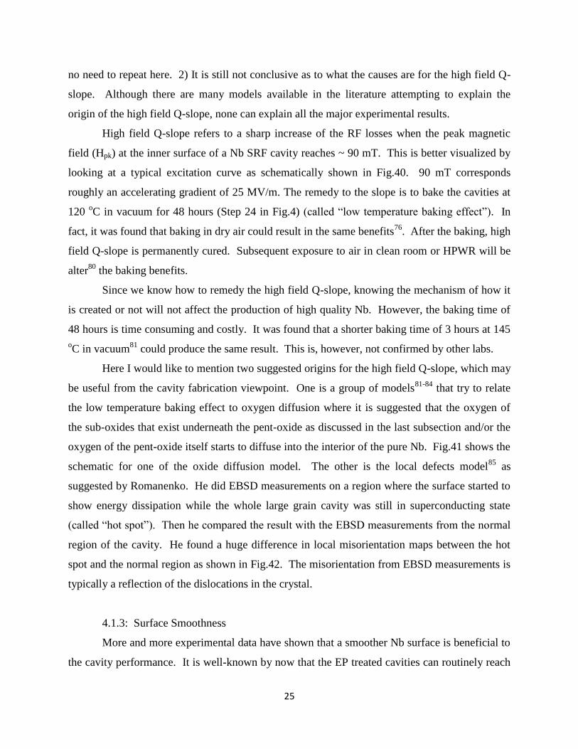
4.1.2: High Field Q-slope
When discussing the requirements in physical properties of Nb for SRF application, one
cannot avoid the discussion of the high field Q-slope that is currently a challenge to the basic
understanding of superconducting properties of Nb in strong RF fields. In this subsection, I will
try to limit my discussion to the very fundamental aspects of high field Q-slope such as, what it
is about, how normally we deal with it, how this will affect Nb handling and cavity production
etc. The reasons for this selection are mainly the following two: 1) there are many updated
review papers76-79
on this topic, which are easily accessible for the interested readers and there is
25
no need to repeat here. 2) It is still not conclusive as to what the causes are for the high field Q-
slope. Although there are many models available in the literature attempting to explain the
origin of the high field Q-slope, none can explain all the major experimental results.
High field Q-slope refers to a sharp increase of the RF losses when the peak magnetic
field (Hpk) at the inner surface of a Nb SRF cavity reaches ~ 90 mT. This is better visualized by
looking at a typical excitation curve as schematically shown in Fig.40. 90 mT corresponds
roughly an accelerating gradient of 25 MV/m. The remedy to the slope is to bake the cavities at
120 oC in vacuum for 48 hours (Step 24 in Fig.4) (called “low temperature baking effect”). In
fact, it was found that baking in dry air could result in the same benefits76
. After the baking, high
field Q-slope is permanently cured. Subsequent exposure to air in clean room or HPWR will be
alter80
the baking benefits.
Since we know how to remedy the high field Q-slope, knowing the mechanism of how it
is created or not will not affect the production of high quality Nb. However, the baking time of
48 hours is time consuming and costly. It was found that a shorter baking time of 3 hours at 145
oC in vacuum
81 could produce the same result. This is, however, not confirmed by other labs.
Here I would like to mention two suggested origins for the high field Q-slope, which may
be useful from the cavity fabrication viewpoint. One is a group of models81-84
that try to relate
the low temperature baking effect to oxygen diffusion where it is suggested that the oxygen of
the sub-oxides that exist underneath the pent-oxide as discussed in the last subsection and/or the
oxygen of the pent-oxide itself starts to diffuse into the interior of the pure Nb. Fig.41 shows the
schematic for one of the oxide diffusion model. The other is the local defects model85
as
suggested by Romanenko. He did EBSD measurements on a region where the surface started to
show energy dissipation while the whole large grain cavity was still in superconducting state
(called “hot spot”). Then he compared the result with the EBSD measurements from the normal
region of the cavity. He found a huge difference in local misorientation maps between the hot
spot and the normal region as shown in Fig.42. The misorientation from EBSD measurements is
typically a reflection of the dislocations in the crystal.
4.1.3: Surface Smoothness
More and more experimental data have shown that a smoother Nb surface is beneficial to
the cavity performance. It is well-known by now that the EP treated cavities can routinely reach

26
an accelerating gradient of 40 MV/m as first pointed out by Visentin76
. The only major
difference that we have found so far between the surfaces treated by EP and BCP is the
roughness. EP treated Nb surfaces are much smoother (see, for instance, Fig.20). Currently, we
know that there are two clear benefits for having a smoother Nb surface. The first one is that it is
much easier to do cleaning on smoother surfaces. The physisorption force is much larger for the
particulates that sit on rougher surface than those that sit on smoother surface. It is been found60
by SFEM that there are fewer field emitters on smoother surfaces than those on rougher surfaces.
Therefore cavities with smoother inner surfaces can pass the obstacle of field emission relatively
easily. The second point is that rougher surface may create local enhancements in magnetic
field86
that has been suggested as one of the mechanisms responsible for causing energy
dissipations at high field.
A remarkable insight on this topic was presented by Saito in Ref.87 where he did
quantitative calculations by assuming a dependence of thermodynamic critical field on the
magnetic field enhancement factor. He was able to demonstrate that in order to reach an
accelerating gradient higher than 30 MV/m the surface smoothness much be better than 2 µm.
To the best of my knowledge, currently the smoothest Nb surface was obtained39-41
by BEP at
Peking University where a root mean square (RMS) of 20 nm was measured over a surface area
of 200x200 µm2.
To summarized up so far for this section, we know that high quality Nb cavities can be
manufactured if the cavities contain less Nb sub-oxides, have very smooth inner surfaces (should
be less than at least 2 µm), and should be fully annealed to remove defects among other
requirements that will be discussed in the following (In the chapter, I will not discuss cavity
optimization from geometry calculations).
4.2: Requirements in Chemical Properties
It is a common practice to give a specification on the chemical composition when
purchasing Nb from manufacturers. This is because the performance of a Nb SRF cavity
depends critically on the chemical composition of Nb. Surface oxygen contain discussed in the
previous section in one example. It is known that interstitial oxygen of several at% can strongly
depress superconductivity in Nb. Tables 3&4 are typical examples of the specifications for
impurity concentrations of Nb for spallation neutron source (SNS) project. To understand the
27
specifications better, I feel that it is very useful to know the production process of Nb. This can
be easily visualized by a Nb production flow chart as shown in Fig.43. Nb ingots are first
produced. Then they are forged and rolled to form sheets for delivering to SRF users. Typically
the thickness of Nb sheets delivered to JLab is either 3 or 4 mm.
4.2.1: Q Disease
One deadly element in Nb that can cause detrimental effect on its RF performance is
hydrogen. It is found from many cavity tests that slow cooling of a cavity in the temperature
range from 100 K to 150 K can degrade the quality factor up to two orders of magnitude. This is
caused by the formation of harmful η and ν phases of niobium hydrides (called Q disease).
The harmful niobium hydrides can only form when the concentration of hydrogen in Nb
exceeds 100-200 at ppm. From Table 4, we can see that normally the impurity contain of
hydrogen of the as-received Nb sheets is below 10 ppm. Why can the Q disease still take place?
This is due to the following two reasons: a) At a temperature between 100 and150 K, the
mobility of hydrogen atoms can reach 5 µm/min. A slow cooling through this region will allow
hydrogen to migrate and gather. At some localized regions the hydrogen concentration can
exceed 100-200 at ppm so that the harmful phases can be formed. b) Various cavity fabrication
steps in Fig.4 such as, machining, E-beam welding, and surface polishing can result in an uptake
of hydrogen to Nb, leading to an increase in hydrogen concentration in Nb. Normally the Nb
pent-oxide on the top of Nb surface can serve as a barrier for hydrogen to enter to the interior of
Nb. However, during handling and treatments the pent-oxide layer can be damaged or removed
(for instance, Step 15). Hydrogen can then start to move in. Hydrogen is also generated during
the reaction of Nb with water as shown in Formula 13. Therefore, the hydrogen concentration in
a fabricated Nb SRF cavity is always much higher than 10 ppm. Q disease was first reported88
by Bonin and Roth.
One can avoid Q disease by cooling through the dangerous temperature region of 100-
150 K quickly and warming up quickly too. Baking at an elevated temperature can remove
hydrogen too (Step 14 in Fig.4). For instance, at JLab cavities are normally baked at 600 oC for
10-12 hours to remove hydrogen.
4.2.2: Effect of Impurity Concentration on Thermal Conductivity
28
One of the major reasons for requiring high RRR Nb for SRF applications is the desire to
have a high thermal conductivity, since thermal conductivity (κ) of Nb at 4.2 K is related to RRR
approximately89
by:
κ = 0.25 (W/m-K)xRRR (15)
More precise relationship between κ and RRR in a wide temperature range can be found in
Ref.90. From Formula 15, we can see therefore high RRR Nb will allow the heat generated
during accelerator operator to be effectively removed by liquid helium. This will result in a
more stable accelerator that is more sustainable for thermal instabilities caused by microscopic
defects that are the major cause for low field quenches. The reason for this is the following:
Simple model calculations have shown that the maximum surface magnetic quench field (Hq) of
Nb is given91
by:
Hq =
(16)
Here Tb is the temperature of the bath to that the cavity is immersed, r is the radius of a
microscopic hemispherical defect, Rn is the surface resistance of the defect. Typical κ for RRR
Nb is 75 W/mK at 4.2 K.
So generally speaking, higher RRR and purer Nb are beneficial to the cavity
performance. A typical RRR value of 300 or higher is required currently for SRF applications
with Ta concentration below 500 ppm. However, the higher is the RRR, the more expensive is
the price, which is especially true92
for Ta since it is not easy to separate Ta from Nb due to the
similarity in many properties between these two elements. Reactor grade of Nb (RRR ~ 30) is
much cheaper than RRR Nb with a low Ta concentration. Therefore one has to ask the question
about whether the specification on Ta is too restricted and whether RRR has to be that high. To
answer these two questions, it is helpful to look at Table 5 where the contributions of different
impurities on RRR of Nb are shown as a percentage of the influence of nitrogen (from Ref.93).
We can see here that contribution from Ta is the second smallest and is twenty times less than
29
that of N. Furthermore, from Table 3 we can see that the specification for Ta concentration for
the Nb used for SNS is 1000 ppm and SNS has been running fine up to now.
In fact, a systematic study of the effect of Ta concentration on cavity performance has
been carried out94
. It was found that when 160 wtppm<Ta<1300 wtppm, 35.9 MV/m>Eacc>26.5
MV/m and 15x109>Qo>6.4x10
9 could be achieved after post purification at 1250
oC in a Ti box
for 12 hours and subsequently held at 1000 oC for 24 hours prior to cool down to room
temperature. A typical example of excitation curves94
measured on a single cell cavity made
from a Nb sheet of Ta concentration of 1300 ppm is shown in Fig.44.
The impurities in Nb can be reduced substantially by heating Nb to 1250 oC or higher
under ultra high vacuum and in a Ti enclosure for a period of time up to 24 hours. At DESY,
this is normally done at a temperature between 1350 oC to 1400
oC for 4 hours. Ti serves here as
a getter material for N, O, CO2, water vapor, and methane. Even at a temperature as low as 700
oC, Ti can start to absorb N up to 90 at% and O up to 50 at%. The absorption ability of Ti to N
increases significantly above 1000 oC due to a phase transition in Ti.
One would naturally concern about the possibility of contaminating Nb by Ti during the
purification process. As reported in Ref.95, the diffusion (D) of Ti into Nb is given by
D = 0.099 exp (-86930/RT) [cm2/sec] (17)
when 994 oC ≤ T ≤ 1492
oC. Here R is the gas constant 8.314 J/(mol K). Using Fick’s law, one
can calculate the concentration of Ti as a function of time and temperature. At 1250 oC, Ti
concentration has dropped to 10-5
in a depth of 5 µm by assuming 6 hours diffusion time. Such a
thickness can be easily removed by, for instance, BCP.
From the discussion in this section, we can see that the requirements in chemical
properties of Nb depend on the applications that one has in mind. If an application does not need
to have an accelerating gradient higher than 30 MV/m with a Qo around 1010
, Ta concentration
can be higher than 500 wtppm. On the other hand, RRR value does not have too much room to
be selected. As discussed above, RRR is related to the effectiveness of the heat transportation
between the SRF cavities and their cooling bath. RRR is also important for making the cavities
more sustainable to the effects from microscopic defects. Therefore, RRR values ranging from
30
250 to 300 or better are needed for most applications unless one wants to use the technique of Nb
on Cu. For SNS project, typical RRR of as-received Nb sheets ranged from 300 to 400.
4.3: Requirements in Metallurgical Properties
In my view, this topic has been a bit overlooked in the SRF field. Defects such as, for
instance, dislocations, stack fault, non-fully crystallized regions, non-uniform grain size, etc can
degrade cavity performance. One example is the hot spot discussed in Section 4.1.2 which is
found to be related to localized misorientations.
Normally, it is specified that the Nb sheets should be fully annealed before they are
delivered to users. However, the experience from myself shows that this is not always the case.
To illustrate the importance of this topic, I will go some into some depth in discussing a
softening problem that I encountered during SNS project at JLab. All the photos and data
discussed here were published only as a JLab technical note95
and have not been published
elsewhere.
For example, during SNS project I did cross-section examination using MOM on several
samples from different batches of as-received Nb sheets from two different suppliers. On one
sample from one supplier, I saw that it was not fully annealed at all. Only about 100 µm thick on
the surface I could see crystal structures as shown typically in Fig.45a). From the figure, the
trace of rolling process during the fabrication of Nb sheets (see Fig.43) can be easily seen. On
another sample from another supplier, I found that the crystal structure was progressively
becoming bad from the surface. At the region starting about 1 mm from the surface, significant
amount of the amorphous phase showed up as shown typically in Fig.45b). Therefore, if cavities
are made from such Nb sheets after Step 15, the exposed surfaces are either amorphous or having
a grain size significantly different from the surface before the treatment. This can certainly cause
significant scattering in the data of cavity measurements.
At Jlab, we used to do hydrogen outgasing at 800 oC for 1 to 3 hours. However, during
SNS project we found that the cavities under such a treatment were significantly softer than they
were before the treatment. This created significant microphonic effects among others and
needed to be remedied. MOM observations95
clearly showed that grain growth and hydrogen
outgassing were responsible for the softening. This conclusion was reached based on the
following two considerations: a) MOM observations showed that the grain size could grow from
31
45 µm to 85 µm after heat treatments at 800 oC for one hour. From any metallurgical text book,
we know that the yield strength of a polycrystalline metal is related to its grain size via the
following relationship:
σy = σi + 1.414σDl1/2
d-(1/2)
(18)
Here σy is the lower yield stress, σi is the shear stress resisting the movement of dislocations
across a particular slip plane, σD is the shear stress to unpin a dislocation, l is the distance from
the piled-up dislocations at the head of the plastic deformation front held up by a grain boundary
to the nearest dislocation source (called Frank-Read source), d is the diameter of the grain.
Therefore the larger is the grain size, the lower is its yield stress. b) From an early study of the
effect of carbon and silicon concentrations on the stress-strain curves of iron through elongation
experiments in 1988, it was found that the elongation curves could be controlled continuously
from a continuous yield to a yield with a yield plateau and the width of the yield plateau various
regularly with the concentrations of carbon and silicon. TEM observations on a sample during
elongation found that carbon and silicon could act as pinning center for dislocations, creating
therefore many short Frank-Read sources. Since σD in equation 18 is inversely proportional to
the length of a Frank-Read source, as a result the yield strength is higher. Similarly in Nb, 800
oC heat treatment is known to outgas H and other impurities. These H and other impurity
interstitial atoms previously could serve as pinning centers for dislocations were now removed
by the outgasing process, leading therefore to a lower yield strength.
Interestingly in some cases, not all the grains were fully grown and grain size could still
vary from the surface to the interior even after the heat treatment as showed typically in Figs.46
and 47. Some areas also showed preferential grain growth along the rolling direction as shown
typically in Fig.48. Another interesting thing to see is shown in Fig.49 where the arrow indicates
a grain with many pits implying that locally the stresses were not completely released by 800 oC
annealing for three hours and there were still many dislocations showing up as the pits on the
surface. Grain growth was found to be much less serious when heat treated at 600 oC
From here we can see that 800 oC heat treatment for 3 hours is too high for hydrogen
outgasing if the stresses stored in the as-received Nb sheets or in the fabricated cavities are not
fully released. This was the base why the 800 oC treatment for 3 hours was changed to 600
oC
32
for 6 hours after SNS project at JLab for hydrogen outgasing. In fact, it is better to outgas H at
650 oC since in this way one can remove unwanted stresses in Nb too while recrystallization can
be largely avoided (see Table 1)
Based on my experience through doing metallographic observations on Nb, I recommend
strongly to use MOM cross-section observation as a quality control tool for both Nb users and
manufacturers as I suggested in Ref.95. One should check whether a Nb sheet is fully annealed
and whether the grain size is uniform from the surface to the interior. This can save a lot of
troubles in cavity production and potentially can save a lot of money wasted in doing cavity
fabrications and treatments and testing.
Dislocations and other defects can also lower RRR leading to lower thermal conductivity
for Nb as pointed out in Ref.96. In my personal view, metallurgical properties of Nb have not
been given the attention they deserved in the SRF community. More work is needed in this area.
For more information about dislocation movements, slip systems, and other issues related to
metallurgical aspects of Nb, please read an excellent recent paper96
by Bieler et al.
4.4: Requirements in Mechanical Properties
This topic is, in fact, strongly coupled with the topic discussed above since grain size,
dislocations, interstitial atoms, and other defects can affect mechanical properties of Nb
enormously just as they do on any metal. Therefore it is also quite naturally to give
specifications on grain size and other mechanical properties of Nb when ordering from Nb
supplier. Table 6 shows an example of such specifications for SNS project.
Mechanical properties of Nb can change significantly with the impurity contents and
therefore RRR for the same reason as discussed in the previous section during hydrogen
outgasing process. A study97
of the variations of mechanical properties with heat treatments at
three different temperatures between 1100 oC and 1250
oC was done by Myneni and Umezawa
on reactor grade Nb. A significant variation in yield strength was found as reproduced in Table
7. The as-received Nb had a yield strength of 110 MPar that was reduced to 56 MPar whereas
RRR increased from 68 to 210. Apart from the effect due to RRR, grain growth after the high
temperature annealing could contribute to the reduction in yield strength as shown in Equation
18.

33
Wu and Myneni measured95
yield stress of Nb from two different suppliers as a function
of the inverse square root of the diameter of grain after heat treatments at 800 oC for 3 hours (one
supplier denoted as SNSw1 & SNSw2 RRR=~400, the other as SNSt RRR=~300) as shown in
Fig.50. From this figure, we may extract the following information: a) generally speaking, yield
strength decreases with increasing grain size, b) regular linear dependence between lower yield
stress and diameter of grain as shown in Equation 18 seems to be followed only when the grain
growth mechanism is the same.
For SNS project, I found that some grains could be huge after heat treatments at 800 oC
for three hours as compared with samples from normal sheets where the average grain size was
ranging from 45 to 51 µm that were a bit below the specifications (see Table 6). A typical
example is shown in Fig.51. Normally exaggerated grain growth is known to occur in one of the
following two ways: a) through a critical strain-anneal treatment, or b) through a process of
secondary recrystallization. A critical strain-anneal treatment is done by making a critical
deformation of a few percent strain to a fully recrystallized sample. Then the sample is subjected
to a high temperature annealing in a thermal gradient along the direction of the deformation.
This situation is hardly applicable to the present situation. We believe that the process of
secondary recrystallization is more likely to occur here, provided that the primary
recrystallization treatment was done at a lower temperature than 800oC. This needs to be
confirmed. For SNSw2 samples, grain growth proceeded steadily for samples under heat
treatments higher than 600oC. However, the difference in grain size between regions close to the
surface and the interior still existed even after the heat treatment at 800oC for three hours (see
Fig.47), but is much less significant than that of the as-prepared sample. We know that the final
grain size of a metal after recrystallization depends on the following factors98
: a) the degree of
prior strain hardening, b) the annealing temperature (above or equal to the temperature that is
required for a complete recrystallization), c) the duration at the annealing temperature, and d) the
rate of heating to reach the annealing temperature. The observation of steady grain growth
seemed to indicate that a substantial amount of strain energy was stored in the as-received SNSw2
sample or the primary recrystallization was done at a temperature lower than 600oC. The later
possibility is highly unlikely since the as-received sample already had some crystals. For SNSt
samples, some grains started to grow and became quite big for all samples under the heat
34
treatment at 800 oC and even for the heat treatment at 600
oC for only three hours. However, they
were not fully recrystallized until heat treatment at 800oC for three hours.
From Fig.50, we can see that the secondary recrystallization tends to change the
dependence dramatically for SNSw1 samples. The two data points of SNSw1 samples fall into the
line for the SNSw1 samples. This may implies that the primary reason responsible for the grain
growth for SNSw2 samples may also be the process of secondary recrystallization. Alternatively,
it can also means that the average grain sizes obtained from these two SNSw1 samples and from
five SNSw2 samples that their data points form a straight line represent their real microstructures
nicely in the same way in terms of their mechanical properties. The one anomalous data point
for SNSw1 samples may be due to the fact that the difference in grain size between the regions
close to the surface and the interior is too much so that an average grain size cannot be obtained
to represent the mechanical properties of the sample. Since there is only one data point for SNSt
sample, it is not meaningful to say anything here except that one should not compare it with data
from SNSw1 and SNSw2. This is because the mechanisms of grain growth can be different
between SNSt and SNSw2/SNSw1. Consequentially, the final state after the heat treatment may
not be the same. In STSt samples, the grain growth started from polygonization, primary
recrystallization, and then grain growth. Besides, the RRR value is also different between STSt
and SNSw2/SNSw1.
A careful mechanical study was also done on Nb with RRR=~300 to study the
relationship between grain size, elongation curve, and annealing temperature as reported in
Ref.99. They found nice variation of the grain size as a function of annealing temperature as
shown in Fig.52. in Fig.53 the corresponding elongation curves are shown. All the samples
were annealed for duration of 4 hours at the different temperatures shown in Fig.53. Similar to
what shown in Fig.50, the yield strength also decreases significantly with the increase in grain
size as shown in Figs 52 and 53.
It is expected that the variation of mechanical properties of Nb at 4.2 K to grain size and
RRR can be different from those at room temperature, since there is a transition of the
workability of Nb from ductile to brittle at ~126 K (see Table 1).
Recently SRF cavities made100,101
from large/single grain Nb have attracted quite some
attentions. This is a very attractive approach since one can skip several steps in Nb production
procedure (see Fig.43) for SRF community. Nb manufacturers can deliver Nb ingots instead of
35
sheets, provided that the ingots are large enough for making SRF cavities. In fact, progress in
Nb production technology in industry makes it possible to make Nb with ingot sizes ranging
from 300 to 500 mm. This is larger enough for making most shapes of high frequency SRF
cavities. For instance, a TESLA shape cavity needs only a disk of 265 mm diameter.
Furthermore, it has been demonstrated100
that an accelerating gradient as high as 45
MV/m is possible for a 2.3 GHz single grain Nb single cell cavity. The mechanical properties of
large/single grain Nb are different from those of regular Nb with grain size of ASTM 4 or 5.
Fig.54 shows typical elongation curves for single grain and polycrystalline RRR Nb, showing
excellent ductility for the Nb single crystal. The stress-strain curve for Nb single crystal even
has a yield plateau similar to what unusually found on fine grain metals. It is rather surprising to
see this since normally the elongation curves of high purity single crystal metals show a
continuous yield since there are not grain boundaries to hinder and not enough pinning sizes to
pin the movements of dislocations generated by the plastic deformation as discussed in Section
4.3.
The effect of RRR and Ta concentration on the mechanical properties of as-received and
high temperature treated Nb single crystals was reported in Ref.101 as reproduced in Fig.55.
Here we can see typical elongation curves for single crystal metals with some impurities serving
as pinning sites for dislocations. It is not clear that witch curve corresponds to which Ta
concentration from Fig.55. I would assume that a higher yield strength come from a higher Ta
concentration.
More controlled and characterized studies of the relationship between mechanical
properties and grain orientations for Nb single crystals can be found in Refs.96 and 102.
Section 5: Summary and Perspective
This chapter gives an overview on the use of Nb for fabricating SRF cavities to be used
in particle accelerators. It also review several examples of significant progresses made in this
field in the past 10 years from my personal viewpoints. SRF technique based on Nb has been
advancing steadily. One example to illustrate this is the Fig.56 where it shows a plot of achieved
accelerating gradient as a function of year103
. As one can see, improved RF performance also
comes with new ideas and innovations. A significant step jump in gradient can be seen when
HPWR and EP were introduced and widely accepted starting in 1995.
36
Efforts have been made mainly in the following two battle grounds: 1) Try to push the
performance limit of Nb. 2) Try to reduce the fabrication cost of Nb SRF cavities. Currently, it
is possible to obtain Nb SRF cavities with performance close to the limit. For instance, an
accelerating gradient of 59 MV/m has been reported104
on a Nb SRF cavity. However, the
production yield for cavities of gradient higher than 35 MV/m with a decent Qo of 1010
is low
and often cavity performance is limited by field emission. An example to see about this is a
statistic summary of the performance of 9 cells cavities given in Fig.57 where one can see that
the data points scatter a lot. One possible way to improve this among others is to improve the
surface smoothness. One major difference between BCP and EP is the surface roughness (see,
for instance, Fig.58) and so100
is between cavities made from large/single grain Nb and from the
regular grain Nb. Therefore, the ability to produce very smooth Nb surfaces routinely appears to
be highly desirable.
New development in Nb quality control and characterization techniques will enable us to
avoid bad starting materials and can help us understand better the art of cavity fabrication and the
mechanism behind each fabrication step. This can lead to a significantly improved cavity
production yield too and therefore is also highly desirable.
Better and more effective ways to remove the chemical residuals and other contaminants
on the surfaces of Nb cavities also deserve great attention. These help us pass by the field
emission barrier and it is one of the necessary steps that you have to go through in order to
achieve routinely the performance limit of Nb SRF cavities.
Reduction of cavity production cost can also be possible if we really understand better the
metallurgical and mechanical properties of Nb. I feel that efforts in this respect are not enough.
Dislocations, interstitial atoms, stacking faults, secondary phases, embedment of foreign
materials, and other defects can be introduced to Nb SRF cavities during cavity fabrication.
They have to be better understood and controlled. For instance, deep drawing in the cavity
fabrication process cause huge plastic deformation and can introduce many edge or screw
dislocations. Although some of them are removed by annealing at high temperatures during
either hydrogen outgasing process or purification process, many of them still stay (see, for
instance, Fig.49). Those defects and imperfections can degrade RF performance seriously.
Again, I would recommend here that MOM cross-section observation should be used as a quality
control tool for both Nb manufacturers and end users.

37
Looking ahead for the use of Nb in SRF application, one has to turn to Nb alloys that
have higher Tc and/or higher Hc such as NbN, NbTiN, and Nb3Sn in order to achieve higher RF
performance limit. One relatively easier way to reach this is perhaps by thin film coating
technique to create the SIS structure as suggested by Gurevich105
or by generating NbN, NbTiN,
and Nb3Sn on Nb or Cu surfaces. Regarding the way to reduce Nb cavity fabrication cost, Nb on
Cu seems to be promising.
*: [email protected]. Notice: Authored by The Southeastern Universities Research Association,
Inc. under U.S. DOE Contract No. DE-AC05-84ER40150 . The U.S. Government retains a non-
exclusive, paid-up, irrevocable, world-wide license to publish or reproduce this manuscript for
U.S. Government purposes.
38
References:
1. H.A. Schwettman, P.B. Wilson, J.M. Pierce, and W.M. Fairbank, International Advances in
Cryogenic Engineering, Plenum Press, New York, (1965) P88
2. J. Preble et al, Proceedings of the 14th
SRF Conference, Berlin, Germany, (2009) P17
3. K. Hosoyama et al, Proceedings of the 13th
SRF Workshop, Beijing, China, (2007) MO405
4. R.C. York, Proceedings of the 12th
SRF Workshop, Ithaca, USA, (2005) P626
5. http://lcdev.kek.jp/Conf/ICFA2002/brinkmann.pdf
6. J. Mammosser, Proceedings of the 14th
SRF Conference, Berlin, Germany, (2009) P62
7. T. Junquera, Proceedings of the 14th
SRF Conference, Berlin, Germany, (2009) P67
8. H. Weise, Proceedings of the 14th
SRF Conference, Berlin, Germany, (2009) P7
9. R.E. Laxdal et al, Proceedings of the 14th
SRF Conference, Berlin, Germany, (2009) P81
10. http://www.linearcollider.org/
11. http://minerals.usgs.gov/minerals/pubs/commodity/niobium/mcs-2009-niobi.pdf
12. J. Bardeen, L.N. Cooper, and J.R. Shrieffer, Phys. Rev., 108 (1957) P1175
13. K. Schulze, Proceedings of the international Symposium on Niobium, The Metallurgical
Society of AIME, (1981) P163
14. A. Gladun et al, Journal of Low Temperature Physics, 27 (1977) P873
15. A.M. Valente-Feliciano, Proceedings of the 13th
SRF Workshop, Beijing, China, (2007) Tu6B
16. The Fourth International Workshop on Thin Films and New Ideas for Pushing the Limits of RF
Superconductivity, Padua, Italy, (2010)
17. W. Singer et al, Proceedings of the 10th
SRF Workshop, Tsukuba, Japan, (2001) P170
18. V. Palmieri, Proceedings of the 11th
SRF Workshop, Travemunde, Germany (2003) TuP26
19. A.T. Wu, in the book Neural Computation and Particle Accelerators: Research, Technology, and
Application, Nova Science Publishers Inc., New York, USA, (2010) Chapter 9
20. X.Y. Lu, Seminar at JLab, (2010)
21. W. Singer, Proceedings of the 13th
SRF Workshop, Beijing, China, (2007) Tutorial 4A2
22. W. Singer et al, Proceedings of the 8th
SRF Workshop, Padova, Italy, (1998) P850
23. W. Singer et al, Proceedings of the 12th
SRF Workshop, Ithaca, USA, (2005) TuP49
24. A. Farr et al, Proceedings of the 11th
SRF Workshop, Travemunde, Germany (2003) ThP40
25. Y. Iwashita et al, Proceedings of the 14th
SRF Conference, Berlin, Germany, (2009) P297

39
26. Y. Iwashita et al, Phys. Rev. ST Accel. Beams 11, 093501 (2008)
27. W.D. Moller, Proceedings of the 14th
SRF Conference, Berlin, Germany, (2009) P109
28. S. Berry et al, Proceedings of the 11th
SRF Workshop, Travemunde, Germany, (2003) ThP04
29. S. Berry et al, Proceedings of EPAC, Lucerne, Switzerland, (2004) P1000
30. M. Ge et al, , Proceedings of the 14th
SRF Conference, Berlin, Germany, (2009) P384
31. G. Wu, Proceedings of the 14th
SRF Conference, Berlin, Germany, (2009) P491
32. A.T. Wu, http://indico.fnal.gov/conferenceDisplay.py?confId=3118 and seminar at JLab (2010).
33. K. Saito et al, Proceedings of the 4th
SRF Workshop, Tsukuba, Japan, (1989) P635
34. A.T. Wu et al, Applied Surface Science, 253 (2007) P3041
35. V. Palmieri et al, Proceedings of the 14th
SRF Conference, Berlin, Germany, (2009) P463
36. M. Raskovic et al, J. Vac. Sci. Technol. A, 27 (2009) P301
37. A. Lozano-Morales et al, http://www.nasf.org/staticcontent/A.MoralesNobium.pdf
38. J. Delayen et al, Proceedings of the 10th
SRF Workshop, Tsukuba, Japan, (2001) P499
39. S. Jin et al, Phys. Rev. ST Accel. Beams 13, 061001 (2010)
40. S. Jin et al, Proceedings of the 13th
SRF Workshop, Beijing, China, (2007) WEP86
41. E. Wang et al, Proceedings of the 13th
SRF Workshop, Beijing, China, (2007) WEP65
42. F. Eozonou et al, Proceedings of the 14th
SRF Conference, Berlin, Germany, (2009) P772
43. A.T. Wu et al, Proceedings of PAC, Vancouver, Canada, (2009) WE5PFP060
44. X.Y. Lu, Seminar at JLab, (2009)
45. J. Beveridge and A.T. Wu, Report of SURI project, JLab, (2010)
46. F. Eozonou et al, Phys. Rev. ST Accel. Beams 13, 083501 (2010)
47. A.T. Wu, Proceedings of the 11th
SRF Workshop, Travemunde, Germany (2003) ThP13
48. A.T. Wu et al, Proceedings of the 1st IPAC, Kyoto, Japan (2010) WEPEC080
49. A.T. Wu et al, Proceedings of the 14th
SRF Conference, Berlin, Germany, (2009) P755
50. M. Ceccato et al, http://conferences.jlab.org/tfsrf/Thursday/Th2_3-V_Palmieri-TFSRF.pdf
51. L. Vuskovic et al,
http://www.hep.uiuc.edu/LCRD/LCRD_UCLC_proposal_FY06/2_52_Vuskovic_ProgressReport
52. E.J. Taylor, Private communication, (2009)
53. A.T. Wu et al, in the book Neural Computation and Particle Accelerators: Research, Technology,
and Application, Nova Science Publishers Inc., New York, USA, (2010) Chapter 4
40
54. A. Brinkmann et al, Proceedings of EPAC 2006, Edinburgh, Scotland, (2006) P418
55. D.R. Swenson et al, Nuclear Instruments and Methods in Physics Research, Section B: Beam
Interactions with Materials and Atoms, Vol.241 (2005) P641
56. D.R. Swenson et al, Nuclear Instruments and Methods in Physics Research, Section B: Beam
Interactions with Materials and Atoms, Vol.261 (2007) P630
57. A.T. Wu and D.R. Swenson, Proceedings of the 14th
SRF Conference, Berlin, Germany, (2009)
P760
58. Z. Insepov et al, Vacuum, 82 (2008) P872
59. A.T. Wu et al, Phys. Rev. ST Accel. Beams 13, 093504 (2010)
60. A.T. Wu et al, Proceedings of the 1st IPAC, Kyoto, Japan (2010) WEPEC081
61. D.R. Swenson et al, AIP Conference Proceedings, 877 (2006) P370
62. D. Proch et al, Proceedings of the 10th
SRF Workshop, Tsukuba, Japan, (2001) P463
63. D. Reschke et al, Proceedings of the 13th
SRF Workshop, Beijing, China, (2007) TUP48.
64. A. Dangwal et al, Journal of Applied Physics, 102, 044903 (2007)
65. https://srf.jlab.org/SurfaceScienceLab.htm
66. A. Dacca et al, Particle Accelerators, 60 (1989) P103
67. Q. Ma and R.A. Rosenberg, Applied Surface Science, 206 (2003) P209
68. Hui Tian et al, Applied Surface Science, 253 (2006) P1236
69. Q. Ma et al, Journal of Applied Physics, 96 (2004) P7576
70. Hui Tian et al, Proceedings of the 13th
SRF Workshop, Beijing, China, (2007) TUP18
71. Q. Ma and R.A. Rosenberg, Proceedings of PAC, Chicago, USA (2001) P1050
72. Q. Ma and R.A. Rosenberg, Proceedings of the 10th
SRF Workshop, Tsukuba, Japan, (2001)
P368
73. K. Kowalski et al, Proceedings of the 11th
SRF Workshop, Travemunde, Germany (2003)
ThP09
74. A. Chincarini et al, Proceedings of the 10th
SRF Workshop, Tsukuba, Japan, (2001) P382
75. A.T. Wu et al, Proceedings of the 14th
SRF Conference, Berlin, Germany, (2009) P300
76. B. Visentin, Proceedings of the 11th
SRF Workshop, Travemunde, Germany (2003) P199
(TUO01)
77. G. Ciovati et al, Phys. Rev. ST Accel. Beams 13, 022002 (2010)
41
78. P. Bauer et al, Review of Q-slope in SRF Cavities, Fermi Lab Report, TD-05-56, (2006). Can be
viewed from Google Search.
79. A. Romanenko, Proceedings of the 14th
SRF Conference, Berlin, Germany, (2009) P95
80. B. Visentin et al, Proceedings of the 9th
SRF Workshop, Santa Fe, USA, (1999) P198
81. B. Visentin et al, Proceedings of the 12th
SRF Workshop, Ithaca, USA, (2005) TuP05
82. H. safa, Proceedings of the 10th
SRF Workshop, Tsukuba, Japan, (2001) P279
83. J. Halbritter, Proceedings of the 11th
SRF Workshop, Travemunde, Germany (2003) MOP44
84. G. Ciovati, Proceedings of the 13th
SRF Workshop, Beijing, China, (2007) TU102
85. A. Romanenko, Proceedings of the 13th
SRF Workshop, Beijing, China, (2007) TU103
86. J. Knobloch et al, Proceedings of the 9th
SRF Workshop, Santa Fe, USA, (1999) P77
87. K. Saito, Proceedings of the 11th
SRF Workshop, Travemunde, Germany (2003) THP15
88. B. Bonin and R. Roth, Proceedings of the 5th
SRF Workshop, Hamburg, Germany (1991) P210
89. H. Padamsee et al, RF Superconductivity for Accelerators, John Wiley & Sons, (1998) P209
90. F. Koechlin et al, Superconductors Science and Technology 9 (1996) P453
91. Reference 89, P206
92. T. Carneiro et al, Proceedings of the 10th
SRF Workshop, Tsukuba, Japan, (2001) P417
93. K.K. Schulze, Journal of Metals, 33 (1981) P33
94. P. Kneisel et al, Proceedings of PAC, Knoxville, USA (2005) P3955
95. A.T. Wu and G. Myneni, JLab-TN-02-027 (2002)
96. T.R. Bieler et al, Phys. Rev. ST Accel. Beams 13, 031002 (2010)
97. G. Myneni and H. Umezawa, Meteriaux and Techniques, 7-8-9 (2003) P19
98. A.M. Shrager, Elementary metallurgy and metallography, Dover Publications, Inc., New York,
(1969) P22
99. W. Singer, SRF materials workshop, Fermi Lab, (2007)
100. P. Kneisel et al, Proceedings of the 12th
SRF Workshop, Ithaca, USA, (2005) MOP09
101. G. Myneni, Proceedings of the 12th
SRF Workshop, Ithaca, USA, (2005) MOP08
102. D. Baars et al, Proceedings of the 14th
SRF Conference, Berlin, Germany, (2009) P144
103. K. Saito, Proceedings of the 13th
SRF Workshop, Beijing, China, (2007) TU202
104. R.L. Geng et al, Proceedings of PAC2007, Albuquerque, USA (2007) P2337
105. A. Gurevish, Applied Physics Letters, 88 012511 (2006)

42
Figure Captions
Fig.1: Photo of a typical Nb SRF cavity and its schematic side view.
Fig.2: A typical measured surface resistance as a function of temperature for a 9-cell Nb SRF
cavity.
Fig.3: Photo of a spoke cavity.
Fig.4: Flow chart for a typical Nb SRF cavity fabrication steps.
Fig.5: Schematic illustrated the working principle of hydroforming20
.
Fig.6: First double cell seamless Nb SRF cavity fabricated from hydroforming17
.
Fig.7: Excitation curves measured on a single cell seamless cavity after buffered chemical
polishing (bcp) and electropolishing (e-pol)17
.
Fig.8: Photos of various steps during the fabrication of a n1.5 GHz copper cavity by spinning.
Seamless Nb SRF cavities are fabricated in the same way18
.
Fig.9: Typical excitation curves for a single cell seamless Nb SRF cavity measured at 1.6 K.
Before the measurements, this cavity was mechanically grinded for 100 µm, then barrel polished
for 84 hours, vacuum annealed at 750 oC for 3 hours followed by electropolishing for 50 µm and
then high pressure water rinsed18
.
Fig.10: Photo of the first 9 cell Nb SRF cavity fabricated by spinning18
.
Fig.11: Shaped Al cathode fabricated at JLab a) top view, b) side view.
Fig.12: Nb dumbbells a) before BEP treatment, b) after BEP treatment.
Fig.13: Schematic illustration of the working principle of an eddy current scanning device for
SRF applications21
.
Fig.14: Schematic illustration of the working principle of a SQUID scanning device for SRF
applications24
.
Fig.15: Schematic diagram of Kyoto Camera a) and its main components b). The inset shown in
the upper right corner of b) shows the mirror and the pulse motor that drives it. The camera
moves for focal adjustment. The electro-luminescence sheets for illumination are shown in the
lower part of b). (all from Ref. 26)
Fig.16: Overview of Kyoto Camera26
.

43
Fig.17: Example of a quantitative measurement on the defect structure observed at one of the
equator region of a 9 cell Nb SRF cavity. a) shows the photo of the defect taken by Kyoto
Camera. b) shows the profile of the defect after the calculations based on the movement of the
bright point across the defect activated by controlled illumination26
.
Fig.18: A typical example28
of the inner surface of a Nb SRF cavity at the quench site replicated
by the technique developed by S. Berry et al. Top is 3D view. Bottom is corresponding contour
plot.
Fig.19: A typical example of the inner surface of a Nb SRF cavity near the welding zone
replicated by the JLab technique32
. The replica was coated by palladium for 5 nm. The lower
image was taken by an optical microscope on the replica from the heat affected zone. The upper
left is taken on the heat unaffected zone. The upper right is an optical image taken on the surface
of Nb for comparison.
Fig.20: Typical high resolution 3D profilometer scans on the surfaces of: (a) buffered
electropolished Nb, (b) electropolished Nb, and (c) buffered chemical polished Nb. The scans are
plotted with the same parameters for comparison34
.
Fig.21: Nb half cell a) before BEP treatment, b) after BEP treatment for 1800 seconds34
.
Fig.22: Polishing currents42
obtained at 5V for different rotation speeds at 30 oC.
Fig.23: Modern vertical BEP system at JLab. The small photo shows the old vertical BEP
system47
used at JLab in 2002.
Fig.24: Typical excitation curves49
for single cell Nb SRF cavity (regular grain size) of CEBAF
shape treated by BEP.
Fig.25: Typical microscopic photos of Nb a) before polishing, b) after polishing by an ionic
liquid50
(see the text for more details) at 190 oC.
Fig.26: Schematic illustration of a microwave glow discharge system for Nb sample exposure36
.
Fig.27: Photo (right) and schematic drawing of a low flow channel cell used to electropolish
25.4 mm x 25.4 mm x 3 mm Nb coupons via Faradayic Electropolishing37
.
Fig.28: Typical microscopic photo of the surface of a Nb coupon treated by Faradayic
Electropolishing in a H2SO4 electrolyte37
.
Fig.29: Schematic of working principal of GCIB.
44
Fig.30: Typical results of measurements on GCIB treated Nb flat samples done by a SFEM. a) A
Nb sample that was treated by O2 GCIB on one half while the other half was not. b) A sample
that was treated by NF3+O2 on one half while the other half was not. Both Nb samples were
polished by BCP prior to GCIB the treatments.
Fig.31: Mesoscale modeling of a Nb surface irradiated by O2 GCIB treatments where it shows
that the features shown in a) are removed by the treatments as shown in b).
Fig.32: Measured etch rates of Nb treated by NF3+O2, Ar, and O2 GCIB as a function of
acceleration voltage61
.
Fig.33: Photo of the nozzle and CO2/N2 jet during a DIC cleaning of a Nb SRF cavity54
.
Fig.34: The DIC system at DESY: a) Photo of the setup54
. b) Schematic diagram of the setup63
.
Fig.35: Filed emission maps of polycrystalline Nb measured by a SFEM over the same 7.5x7.5
mm2 before (left) and after (right) DIC up to a DC field gradient of 120 MV/m.
Fig.36: Typical oxygen depth profiles from SIMS measured on a BCP treated sample (reference
sample), BCP-treated + baked in air at 120 oC for 12 hours (baking 1), and BCP-treated + baked
in air at 120 oC for 48 hours (baking 2)
Fig.37: Typical deconvolution components of Nb 3d spectrum from XPS measurements68
.
Fig.38: Atomically resolved TEM cross-section image75
of an BCP treated Nb sample obtained
using JEM-2100F.
Fig.39: Schematic of the oxide layer structure on Nb surfaces.
Fig.40: Schematic of the high field Q-slope (see the text for more details).
Fig.41: Schematic illustration of an oxygen diffusion model78
.
Fig.42: Lattice misorientation maps85
for a hot spot (right) and a normal area (left). Please see
the text for more details.
Fig.43: Flow chart of Nb production process (taken from internet).
45
Fig.44: Performance94
of Nb SRF single cell cavity made from high Ta content Nb (1300
wtppm). Shown is Q0 vs. Eacc before heat treatment, after heat treatment and “in situ” baking at
120 oC for 48 hours.
Fig.45: Typical MOM cross-section photos of as-received Nb, a) showing that the sample was
not crystallized, b) showing a variation in microstructure from the surface to the interior,
implying that both samples were not fully annealed after rolling.
Fig.46: An amorphous area was still seen from MOM on one sample cut from a Nb sheet treated
at 800 oC for three hours.
Fig.47: Variation of grain size from surface to the interior observed on one sample cut from a
Nb sheet treated at 800 oC for three hours. a) On the surface. b) On the interior adjacent to the
surface shown in a). The arrow indicates the area with a smaller grain size as compared with that
on the surface.
Fig.48: MOM photo on a sample cut from a Nb sheet that was treated at 800 oC for three hours.
The arrow indicates that locally the stresses in this region were not fully released. There were
still many dislocations shown as pits on the surface.
Fig.49: Typical MOM photo of preferential crystal growth along the rolling direction after heat
treatment at 800 oC for three hours.
Fig.50: Measured yield stress plotted as a function of inverse square root of diameter of grain
size form samples cut from Nb sheets supplied by two Nb manufacturers. (see text for more
details)
Fig.51: Typical example of huge grains observed by MOM on a SNSw1 sample after annealing
at 800 oC for three hours (see text for more details)
Fig.52: Grain size measured99
as a function of annealing temperatures for Nb RRR ~300.
Fig.53: Stress-strain curves99
for the Nb RRR~300 treated at various temperatures (see the
figures) for 4 hours.
Fig.54: Typical elongation curves100
measured on polycrystalline and single crystal Nb.

46
Fig.55: Elongation curves for as-received and high temperature treated Nb single crystals of
different RRR and Ta concentration (see the figure).
Fig.56: History103
of high accelerating gradient of Nb SRF cavities.
Fig.57: Statistics of the performance of 9-cell Nb SRF cavities at DESY.
Fig.58: Typical BCP and EP treated Nb surfaces as seen from a SEM.
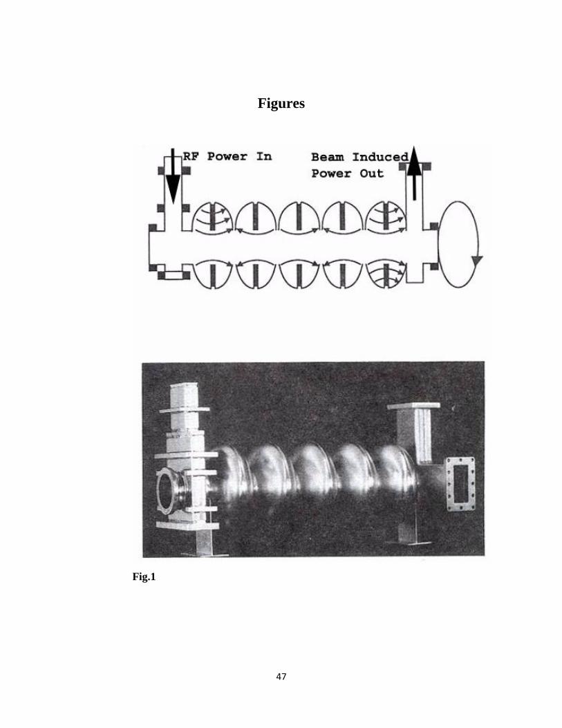
47
Figures
Fig.1
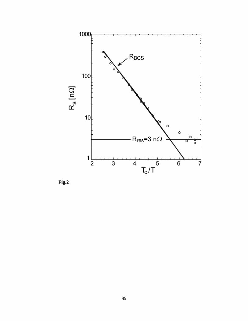
48
Fig.2
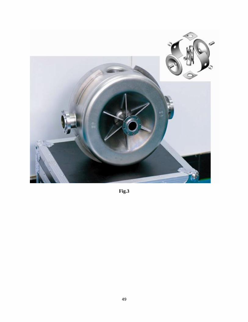
49
Fig.3
50
Fig.4

51
Fig.5
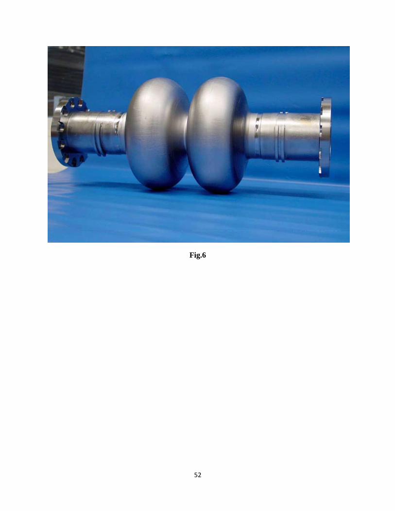
52
Fig.6
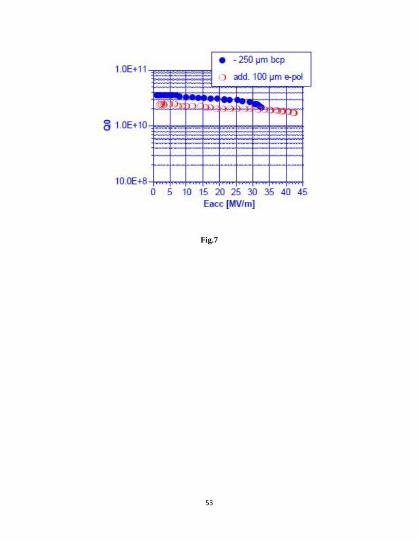
53
Fig.7
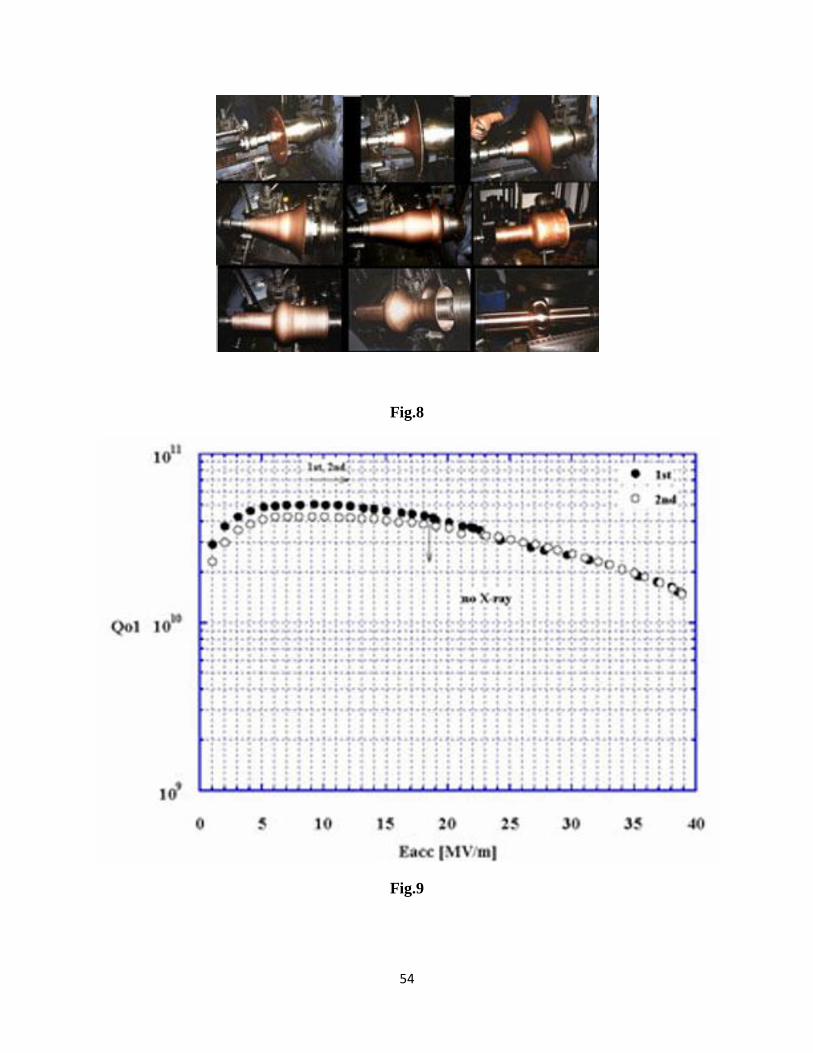
54
Fig.8
Fig.9
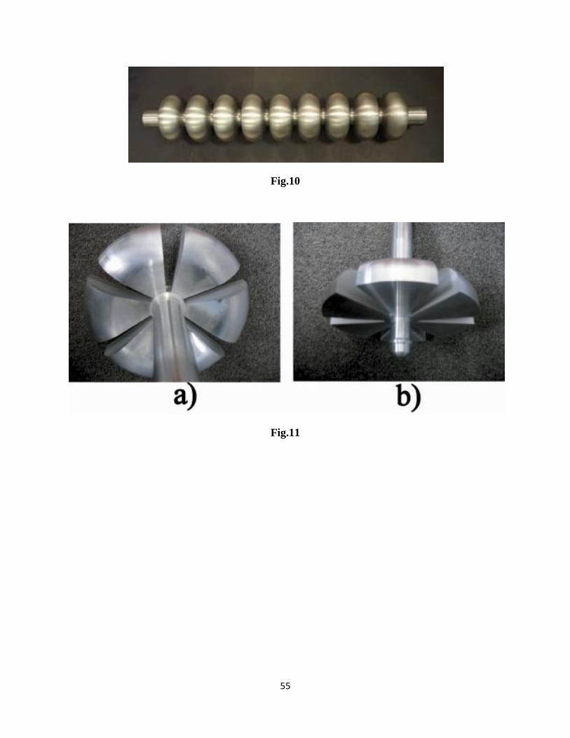
55
Fig.10
Fig.11
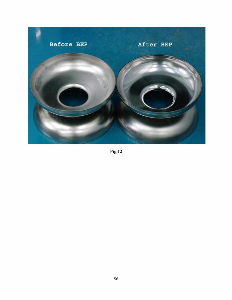
56
Fig.12
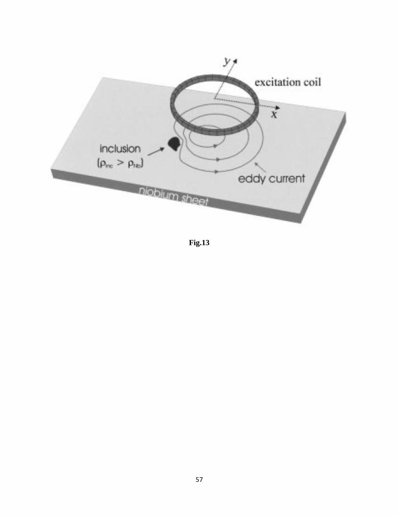
57
Fig.13
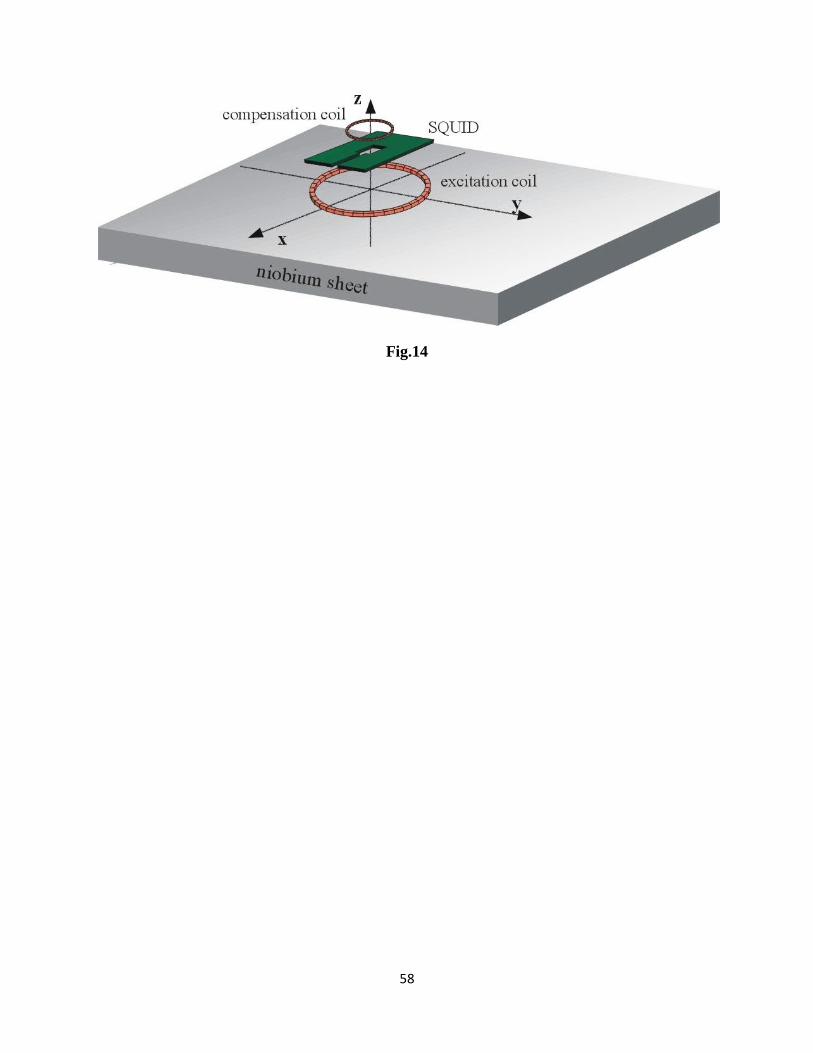
58
Fig.14
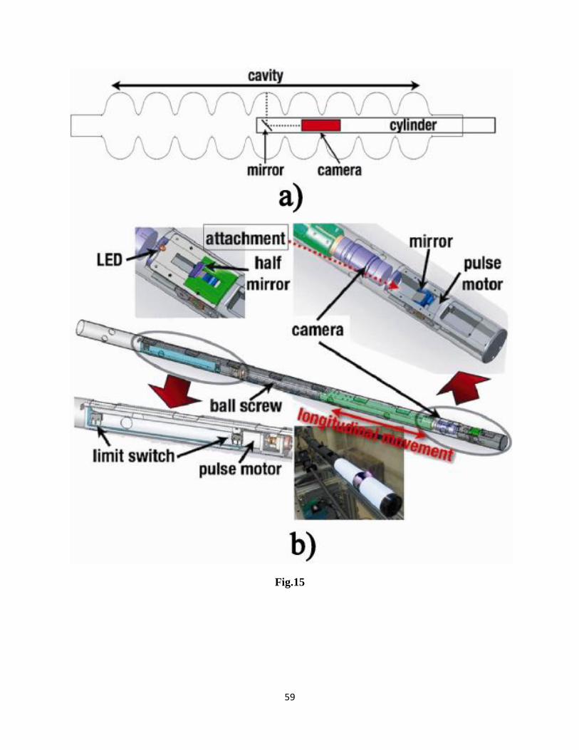
59
Fig.15
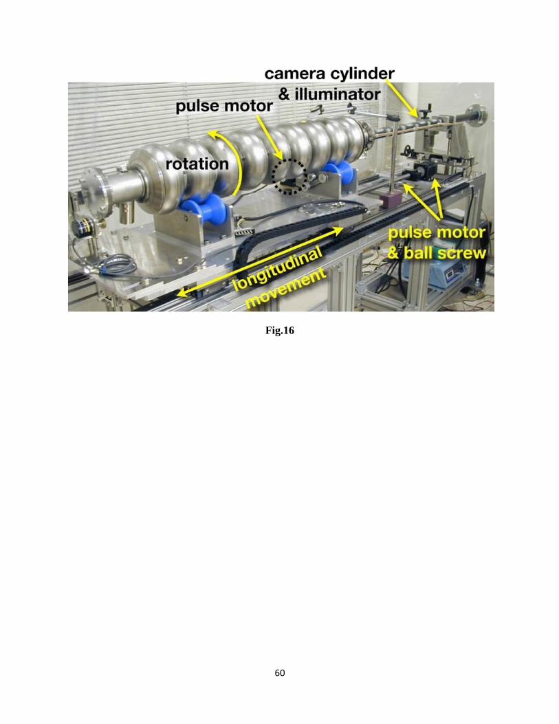
60
Fig.16
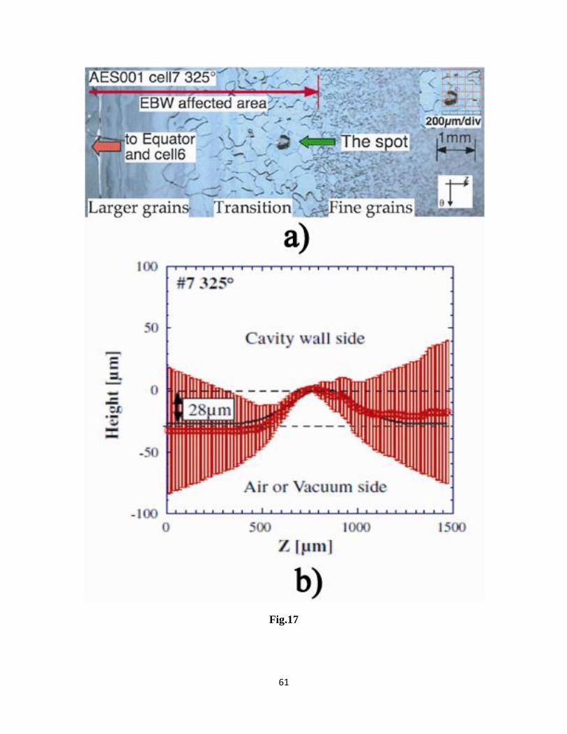
61
Fig.17
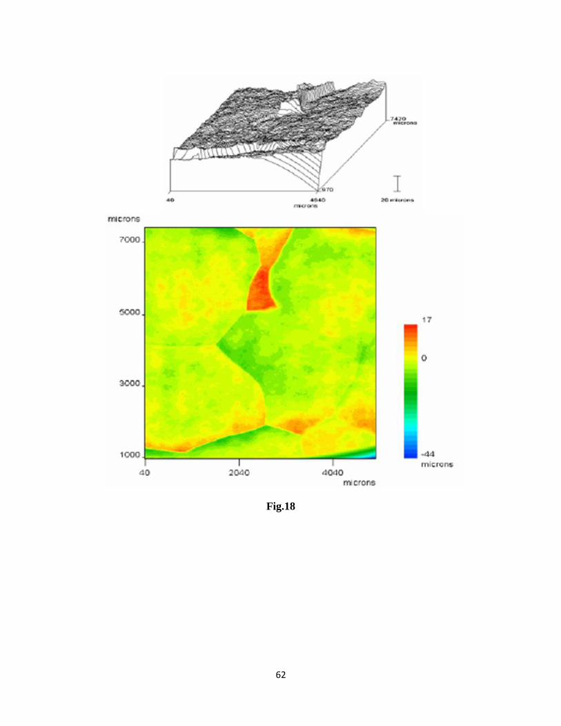
62
Fig.18
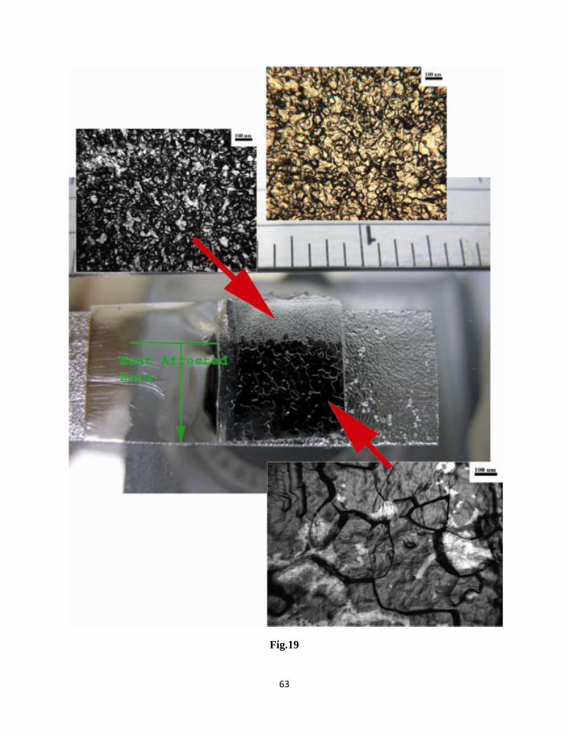
63
Fig.19
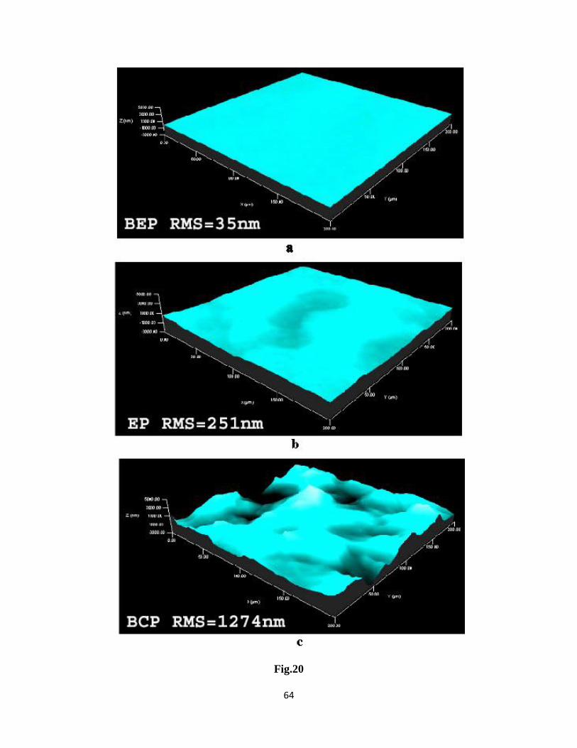
64
Fig.20

65
Fig.21
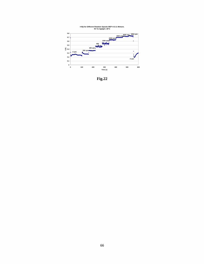
66
Fig.22
I=f(t) for Different Rotation Speeds BEP 4-5-11 Mixture.
5V Vs AgAgCl. 30°C
0
0,1
0,2
0,3
0,4
0,5
0,6
0,7
0,8
0 100 200 300 400 500 600
Time (s)
I (A
)
200 rpm
400 rpm
800
rpm
1200 rpm
2000 rpm
3000 rpm4000 rpm 4994 rpm
0 rpm
0 rpm

67
Fig.23
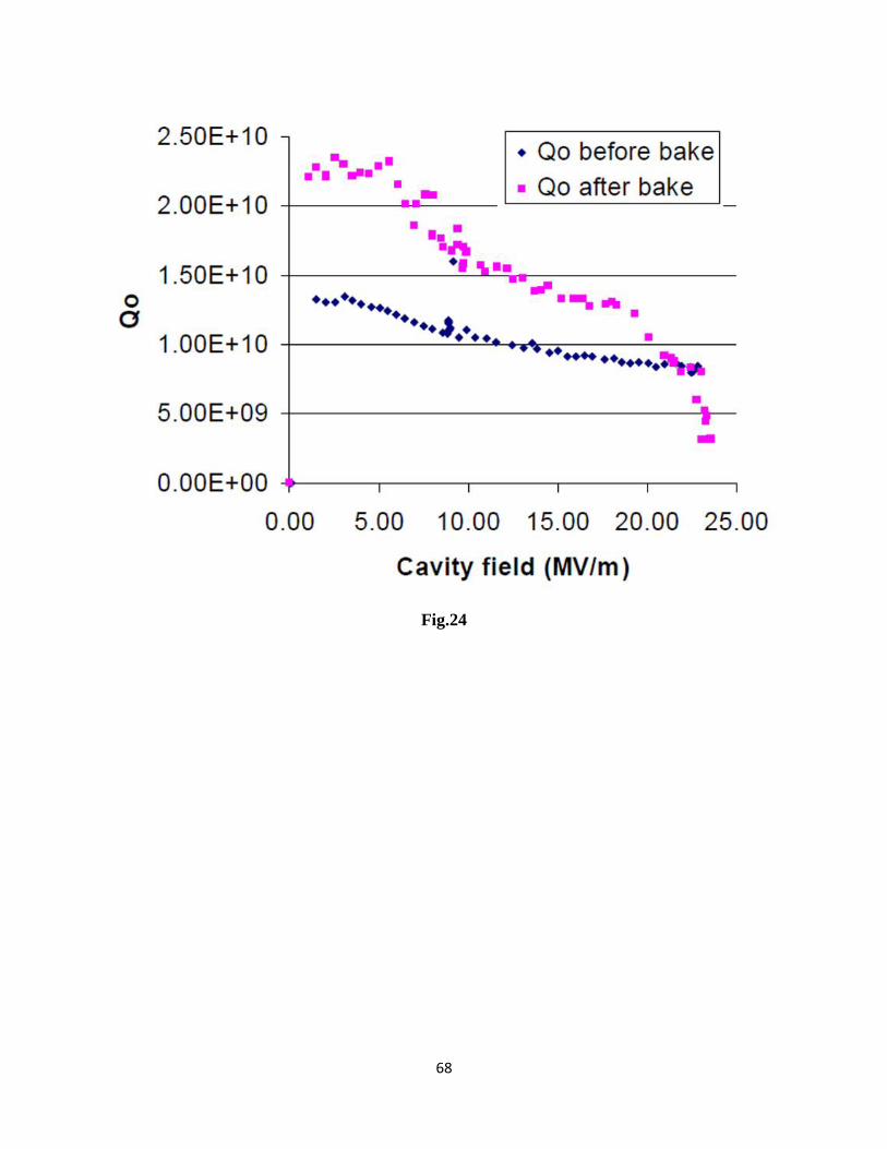
68
Fig.24
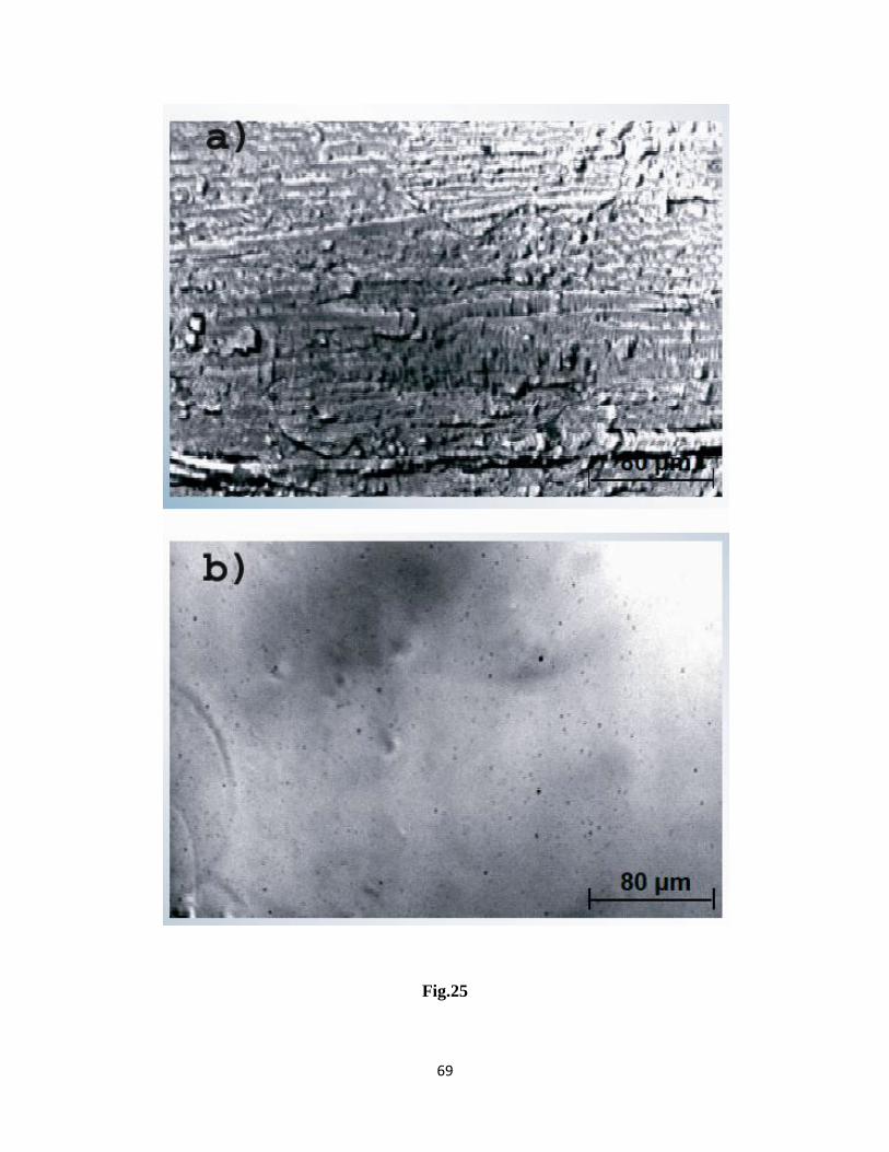
69
Fig.25
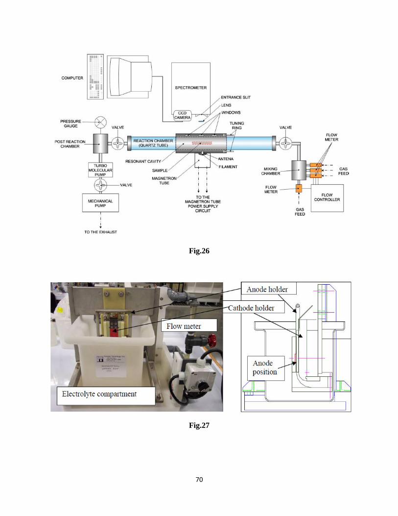
70
Fig.26
Fig.27
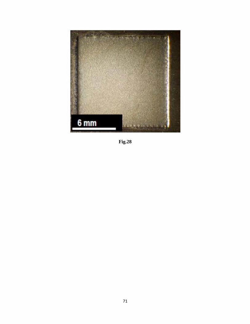
71
Fig.28
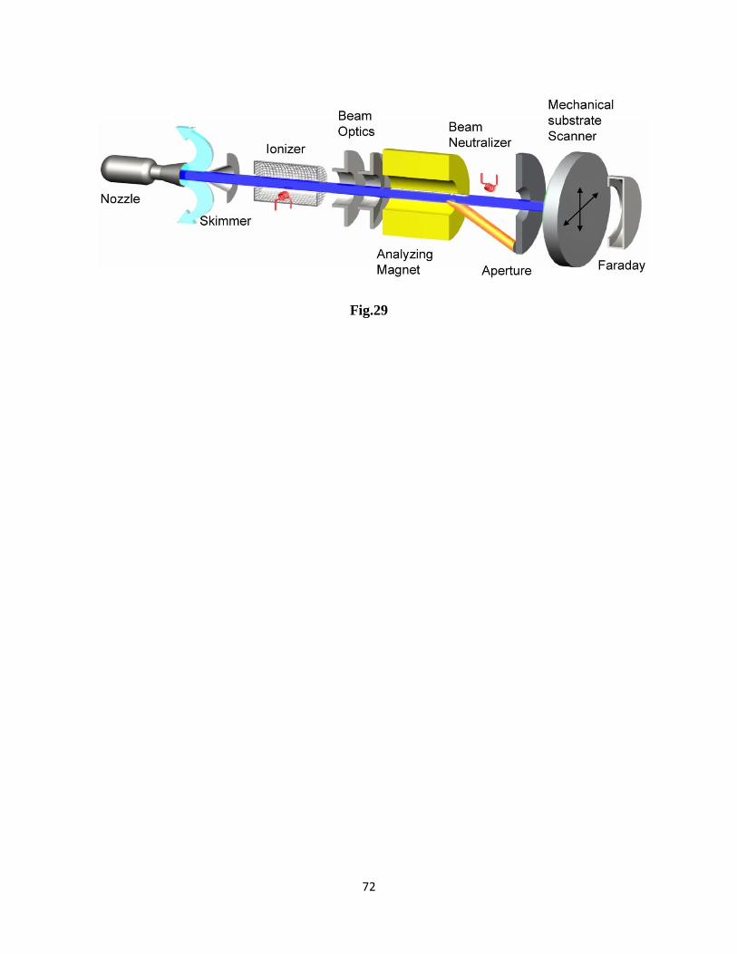
72
Fig.29
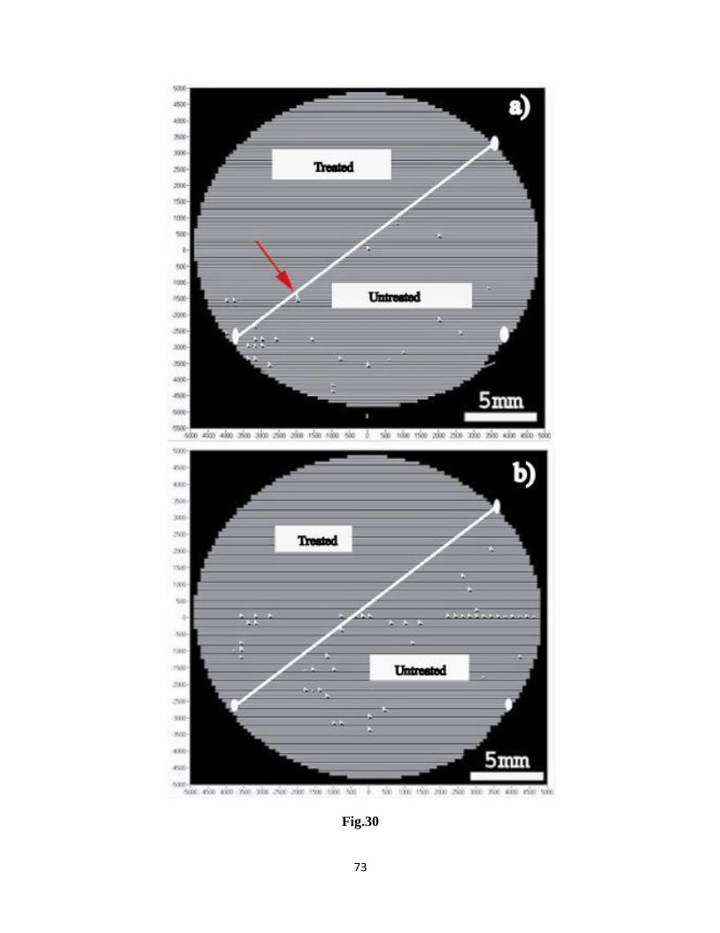
73
Fig.30

74
Fig.31
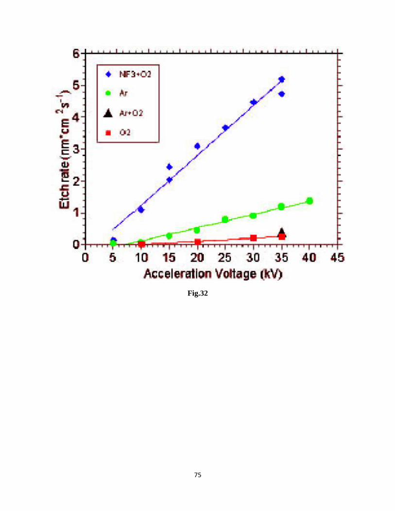
75
Fig.32
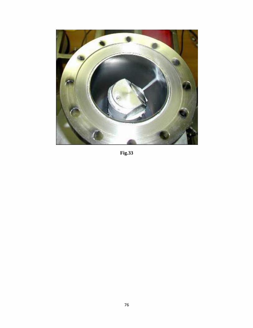
76
Fig.33

77
Fig.34
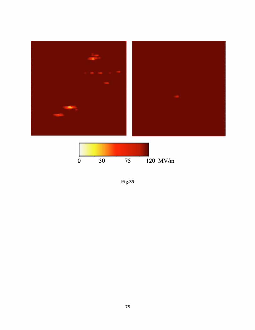
78
Fig.35
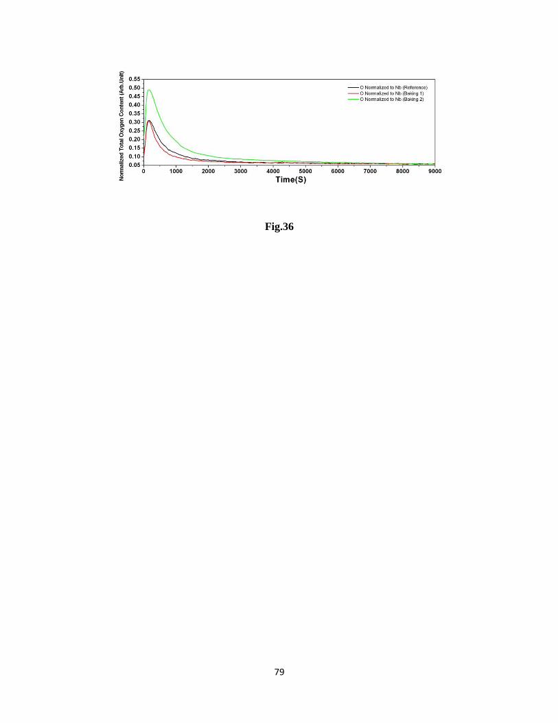
79
Fig.36
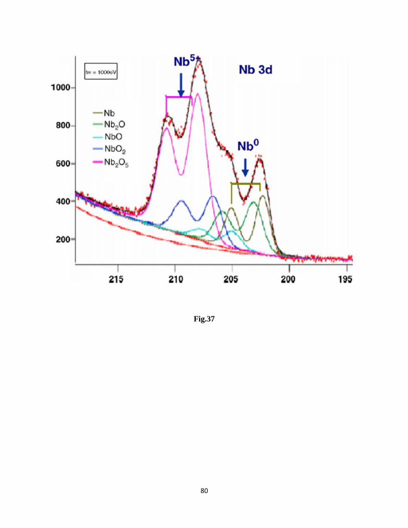
80
Fig.37
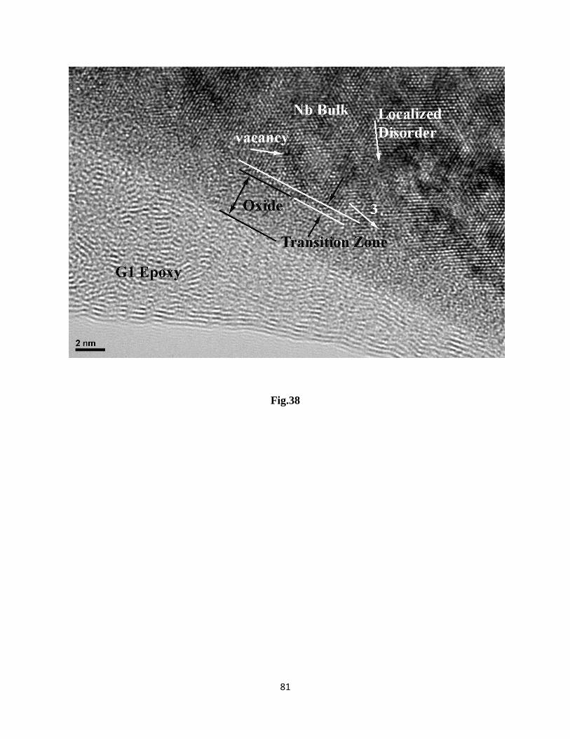
81
Fig.38

82
Fig.39
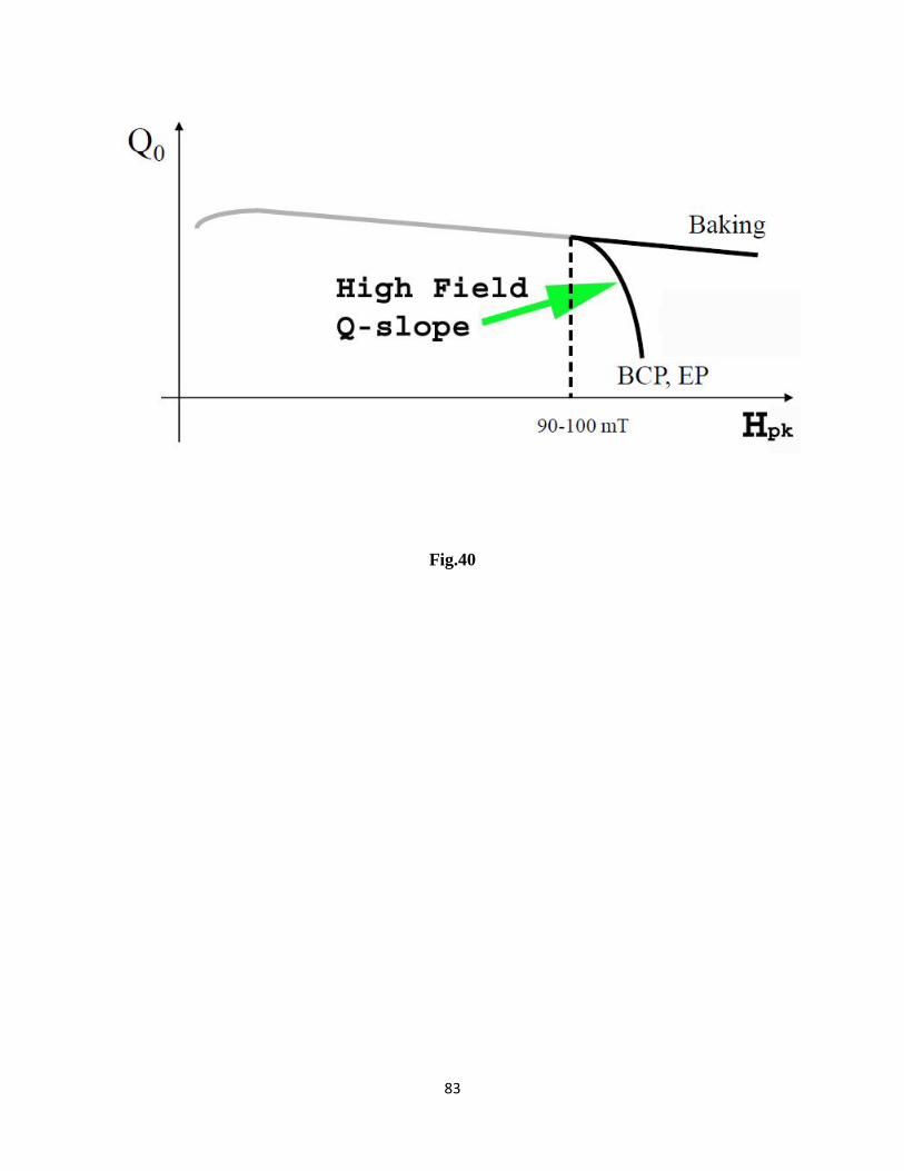
83
Fig.40
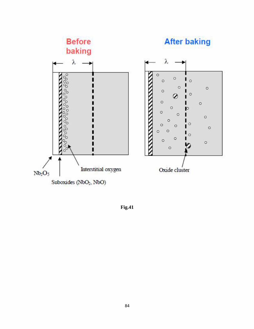
84
Fig.41
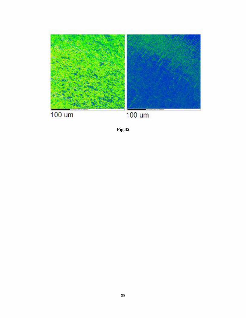
85
Fig.42
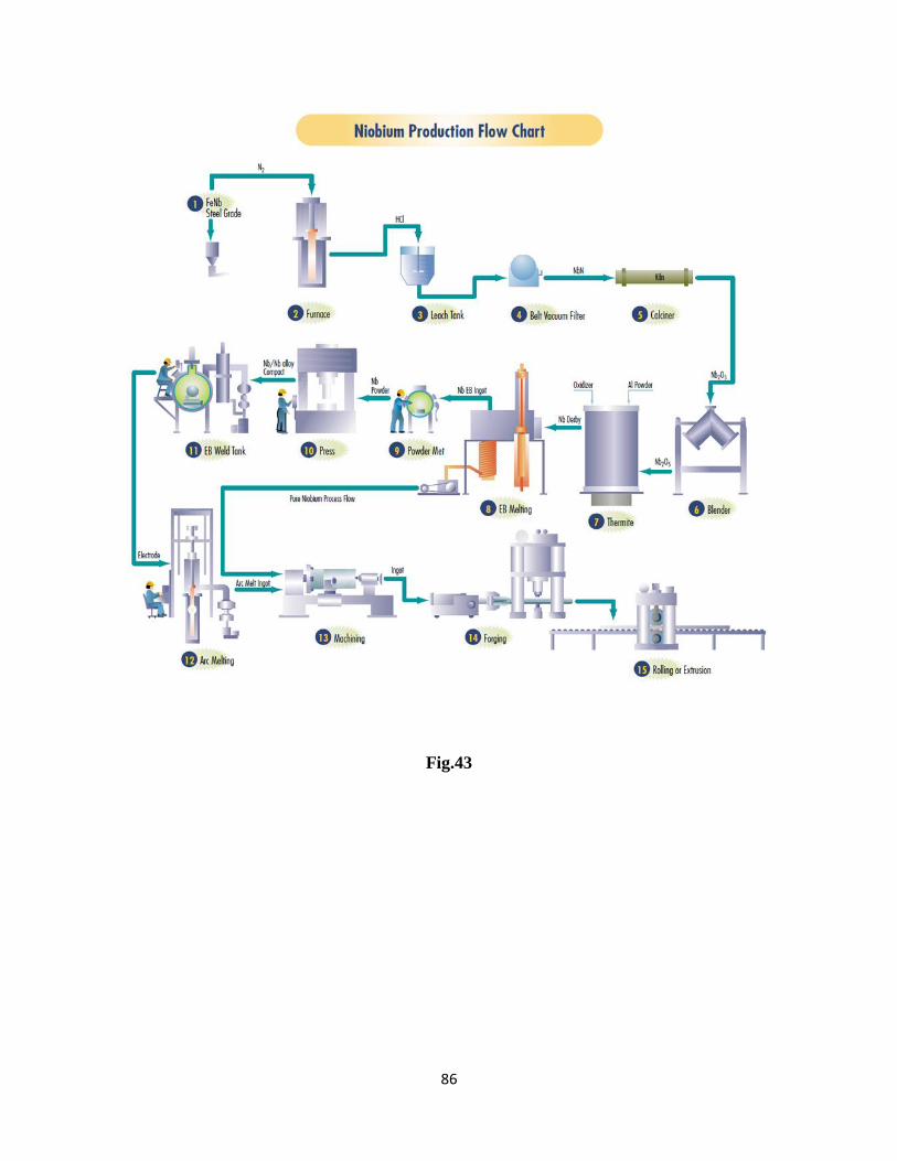
86
Fig.43
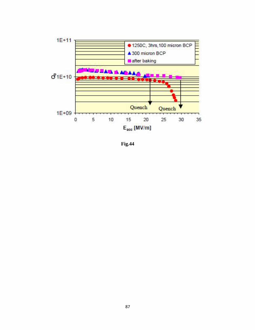
87
Fig.44

88
Fig.45
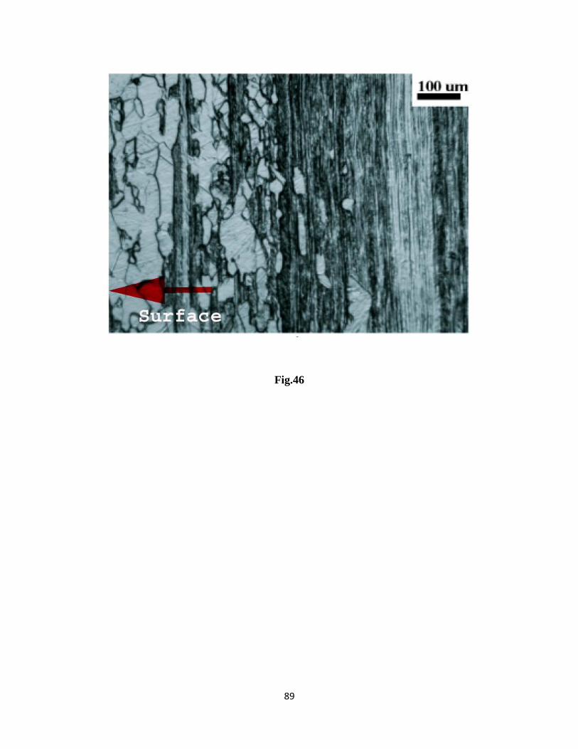
89
Fig.46
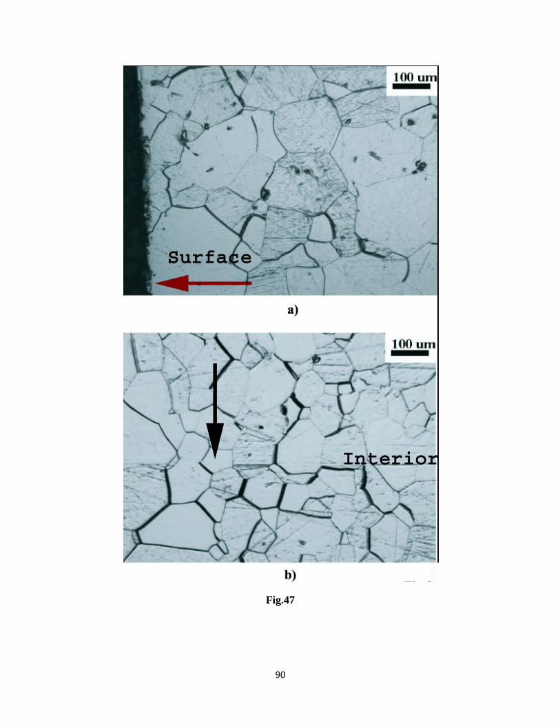
90
Fig.47
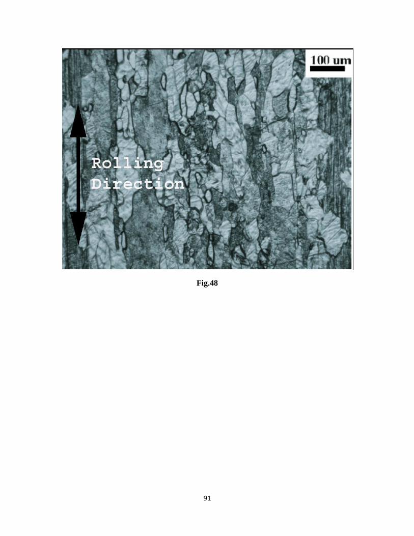
91
Fig.48

92
Fig.49

93
Fig.50
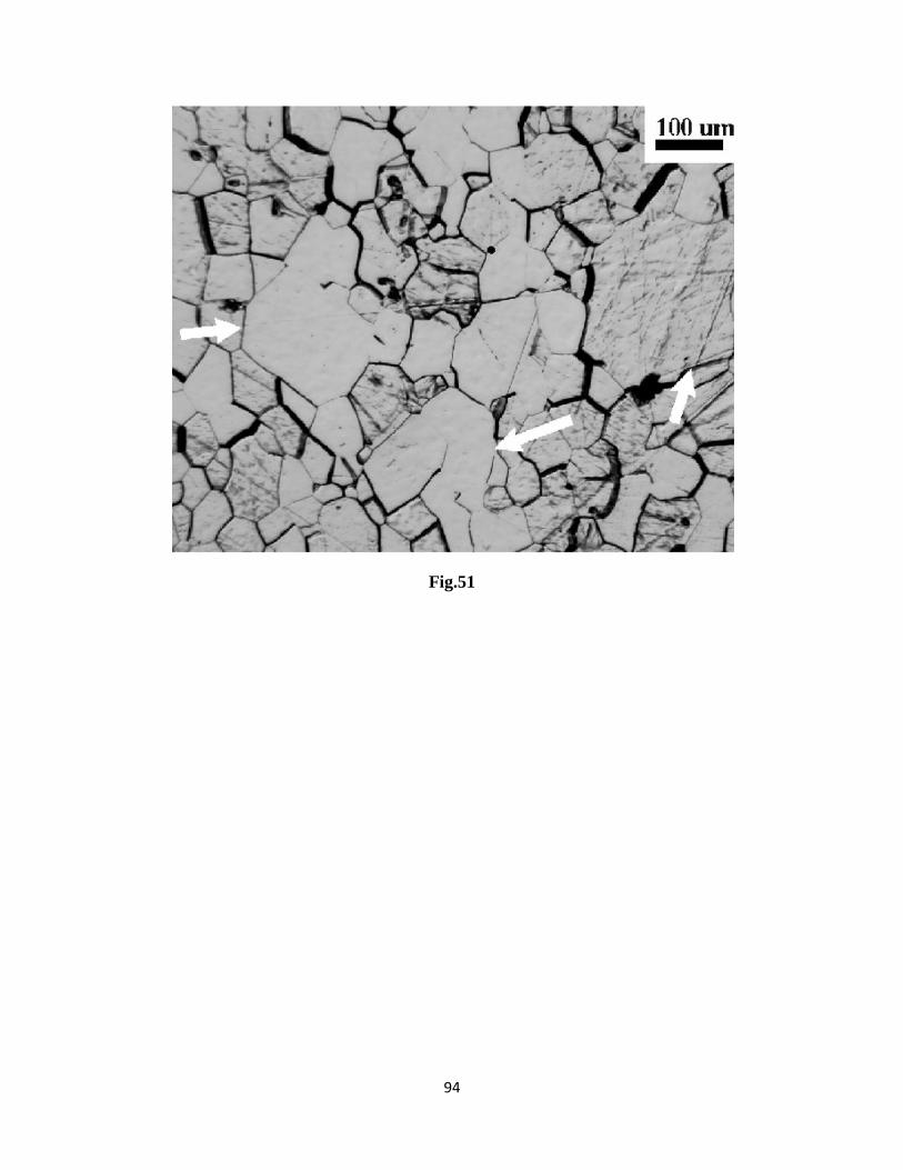
94
Fig.51
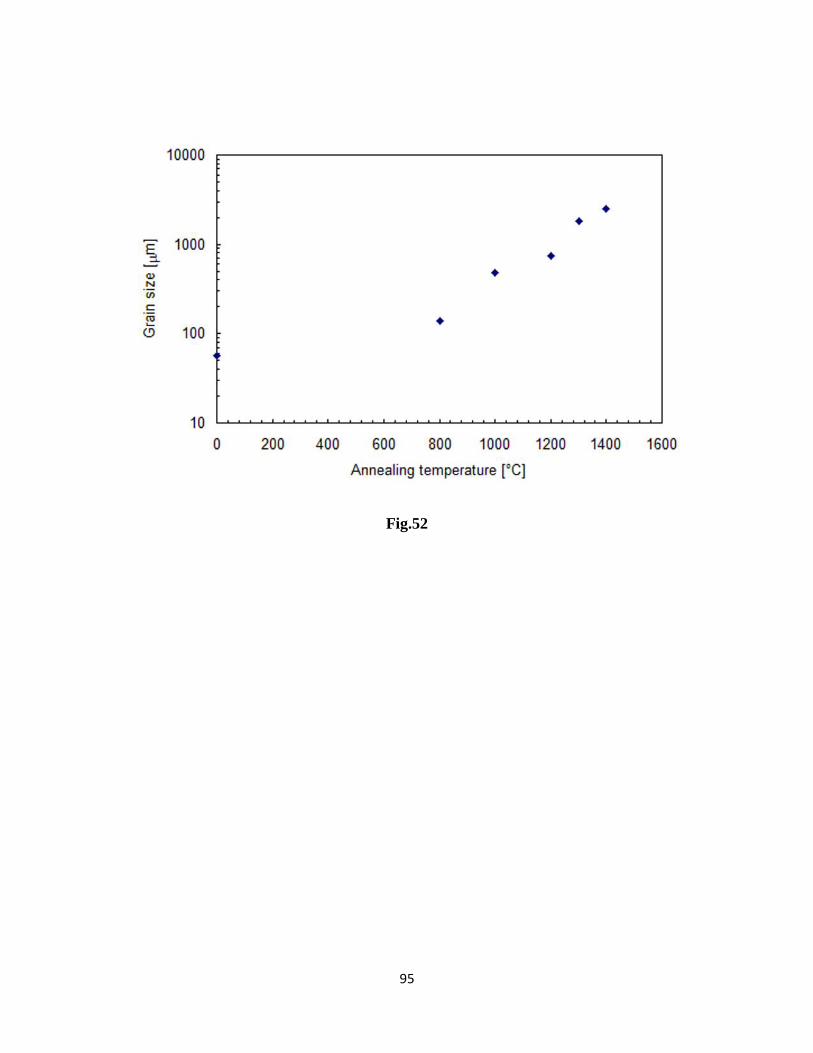
95
Fig.52
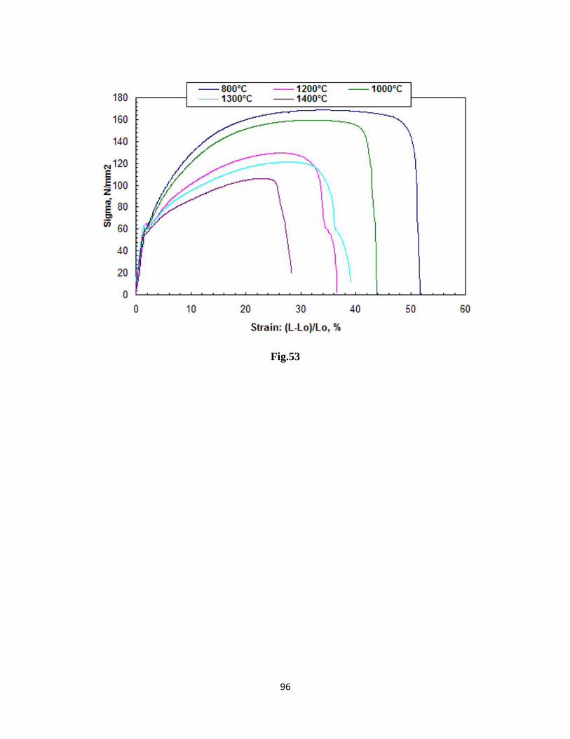
96
Fig.53
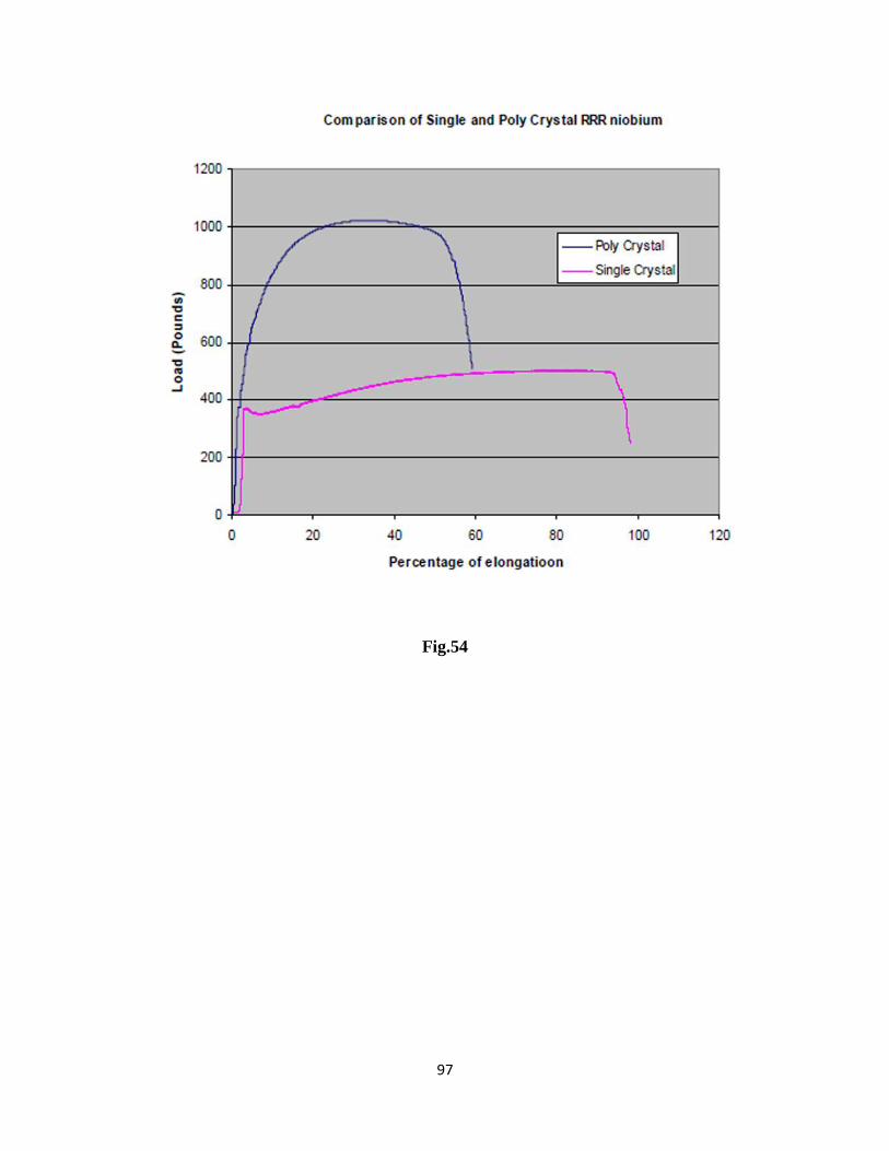
97
Fig.54
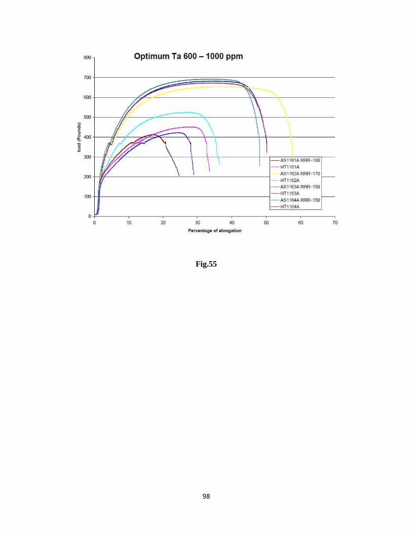
98
Fig.55

99
Fig.56
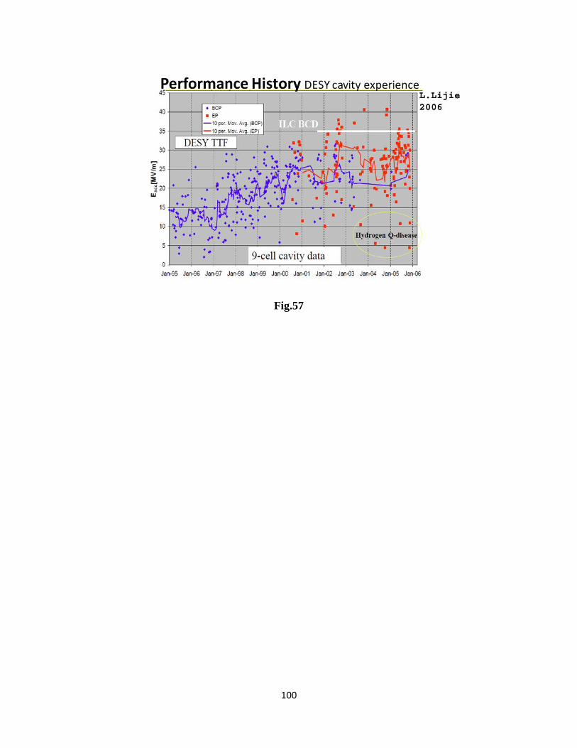
100
Fig.57
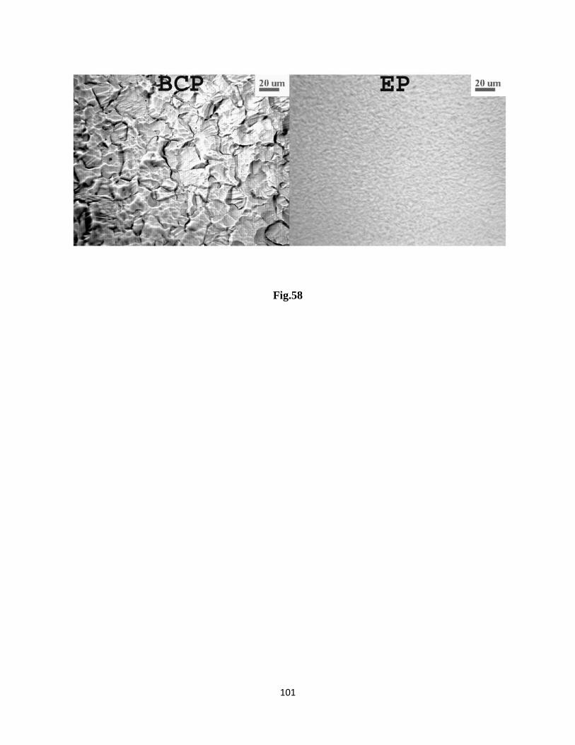
101
Fig.58
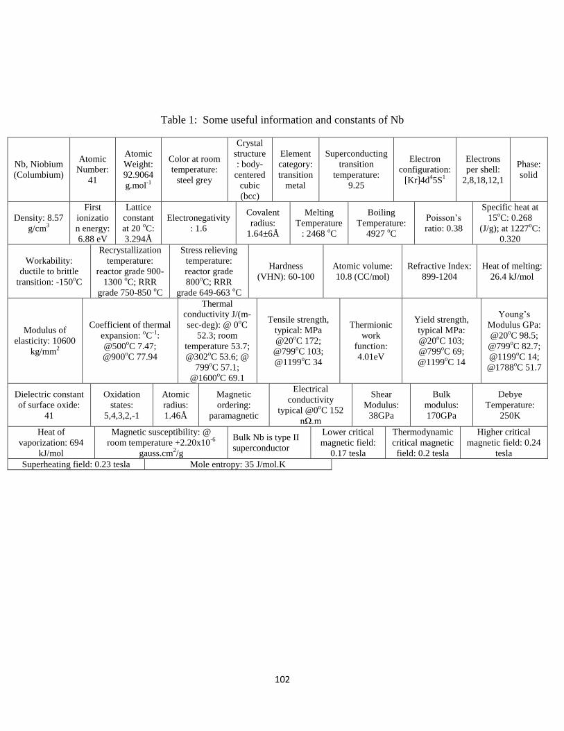
102
Table 1: Some useful information and constants of Nb
Nb, Niobium
(Columbium)
Atomic
Number:
41
Atomic
Weight:
92.9064
g.mol-1
Color at room
temperature:
steel grey
Crystal
structure
: body-
centered
cubic
(bcc)
Element
category:
transition
metal
Superconducting
transition
temperature:
9.25
Electron
configuration:
[Kr]4d45S
1
Electrons
per shell:
2,8,18,12,1
Phase:
solid
Density: 8.57
g/cm3
First
ionizatio
n energy:
6.88 eV
Lattice
constant
at 20 oC:
3.294Å
Electronegativity
: 1.6
Covalent
radius:
1.64±6Å
Melting
Temperature
: 2468 oC
Boiling
Temperature:
4927 oC
Poisson’s
ratio: 0.38
Specific heat at
15oC: 0.268
(J/g); at 1227oC:
0.320
Workability:
ductile to brittle
transition: -150oC
Recrystallization
temperature:
reactor grade 900-
1300 oC; RRR
grade 750-850 oC
Stress relieving
temperature:
reactor grade
800oC; RRR
grade 649-663 oC
Hardness
(VHN): 60-100
Atomic volume:
10.8 (CC/mol)
Refractive Index:
899-1204
Heat of melting:
26.4 kJ/mol
Modulus of
elasticity: 10600
kg/mm2
Coefficient of thermal
expansion: oC
-1:
@500oC 7.47;
@900oC 77.94
Thermal
conductivity J/(m-
sec-deg): @ 0oC
52.3; room
temperature 53.7;
@302oC 53.6; @
799oC 57.1;
@1600oC 69.1
Tensile strength,
typical: MPa
@20oC 172;
@799oC 103;
@1199oC 34
Thermionic
work
function:
4.01eV
Yield strength,
typical MPa:
@20oC 103;
@799oC 69;
@1199oC 14
Young’s
Modulus GPa:
@20oC 98.5;
@799oC 82.7;
@1199oC 14;
@1788oC 51.7
Dielectric constant
of surface oxide:
41
Oxidation
states:
5,4,3,2,-1
Atomic
radius:
1.46Å
Magnetic
ordering:
paramagnetic
Electrical
conductivity
typical @0oC 152
nΩ.m
Shear
Modulus:
38GPa
Bulk
modulus:
170GPa
Debye
Temperature:
250K
Heat of
vaporization: 694
kJ/mol
Magnetic susceptibility: @
room temperature +2.20x10⁻⁶
gauss.cm2/g
Bulk Nb is type II
superconductor
Lower critical
magnetic field:
0.17 tesla
Thermodynamic
critical magnetic
field: 0.2 tesla
Higher critical
magnetic field: 0.24
tesla
Superheating field: 0.23 tesla Mole entropy: 35 J/mol.K

103
Table 2: Popular Instruments Used in the Studies of the Physical Properties of Nb for SRF
Applications: Properties They Probe and Their Characteristics
Instrument SEM TEM SIMS AFM
Properties Detected
imaging
imaging, atomic structure, defects, dislocations,
interstitial atoms,
secondary phases
composition, depth
profile, elemental mapping
imaging, surface
topography and morphology
Characteristics lateral resolution of 1-5
nm lateral resolution down to
0.05 nm
~ppm down to ppb, can
be very surface sensitive
(static SIMS) 5% of the surface top layer, can
measure all elements
including H
lateral resolution down to 1nm, limited scan size
~50 µm2 at room
temperature and smaller at low temperatures
Instrument STM EDX XPS Profilometer
Properties Detected
Imaging, surface topography and
morphology and electron
density of state
elemental analysis, composition, elemental
mapping
composition, electronic structure or chemical
state, depth profile,
elemental mapping
imagine, surface
topography and morphology
Characteristics
lateral resolution down to
0.1 nm, limited scan size
~50 µm2 at room temperature and smaller
at low temperatures, only
works on metallic or semiconducting surfaces
not surface sensitive,
typical probing depth ~
µm, cannot detect elements with atomic
number smaller than Be,
typical sensitivity to impurity ~ 1% (atm)
very surface sensitive,
typical probing depth
<10nm, typical sensitivity to impurity 200ppm
(atm), cannot detect H
lateral resolution down to
5 nm, extremely larger
scan size up to 15x15 cm2 or larger
Instrument MOM SFEM SAM EBSD
Properties Detected
imaging detecting field emitters and imaging, mapping
composition, element,
imaging, depth profile, elemental mapping
crystal orientation,
texture, defects, phase
identification, morphology, orientation
mapping
Characteristics
relatively shallow depth of field (compared with
SEM), lateral resolution >
200 nm
gradient up to 250 MV/m
with lateral resolution ~2.5 µm
very surface sensitive, typical probing depth
<10nm, typical sensitivity
to impurity 0.1% (atm), cannot detect elements
with atomic number
smaller than Be
surface sensitive, probing
depth 10 nm-50 nm,
lateral resolution for mapping can be down to
10 nm
104
Table 3: Requirements for the impurity contain of Nb ingots
Element Ta W Ti C O N H Fe Max Parts per Million weight
(ppm) 1000 100 40 30 40 30 10 50
Element Si Mo Max Parts per Million weight
(ppm) 50 50
Table 4: Requirements for dissolved interstitial elements of Nb sheets
Element O N C H Max Parts per Million
weight (ppm) 40 30 30 10
Table 5: Relative influence of different impurities on RRR of niobium (from Ref.93)
Element N C O H Ti Hf Zr W Mo Ta
Percentage 100 83 87 15 27 27 12 to 27 8 to 21 4 5
Table 6: Specifications on mechanical properties of Nb for SNS project
Yield Strength
(0.2% offset)
Tensile Strength
Elongation (1 inch gauge
length)
Hardness, HV 10
Recrystallization Grain Size (d)
7000 psi (48.2
N/mm2) minimum
14000 psi (96.4
N/mm2) minimum
40% minimum
longitudinal, 35%
minimum transverse
50 maximum
90% ASTM4
(90µm)>d>ASTM5(64µm)


![Fast and Efficient Synthesis of Pyrano[3,2- c ]quinolines Catalyzed by Niobium(V) Chloride](https://static.fdokumen.com/doc/165x107/6337c72f65077fe2dd044087/fast-and-efficient-synthesis-of-pyrano32-c-quinolines-catalyzed-by-niobiumv.jpg)