Tunable T-Shaped Waveguide in Two Dimensional Photonic Crystals Based on Liquid Crystals
Upload
khangminh22Category
view
0download
0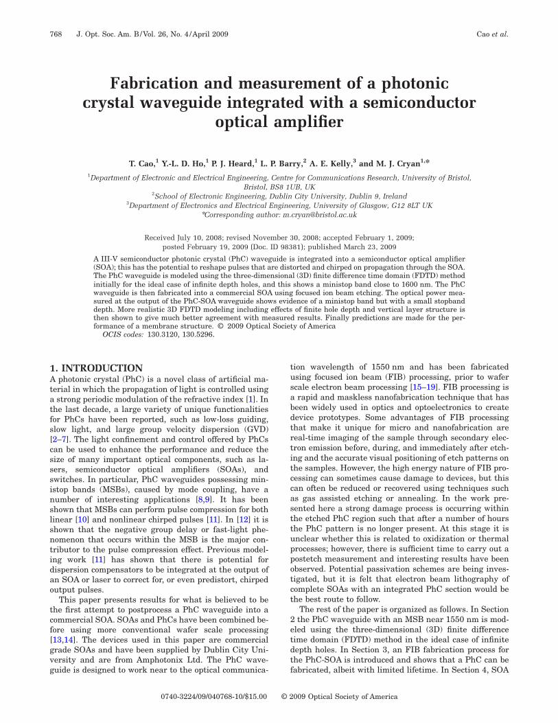
1Atatfs[csssinslsntidao
tcf[gvg
768 J. Opt. Soc. Am. B/Vol. 26, No. 4 /April 2009 Cao et al.
Fabrication and measurement of a photoniccrystal waveguide integrated with a semiconductor
optical amplifier
T. Cao,1 Y.-L. D. Ho,1 P. J. Heard,1 L. P. Barry,2 A. E. Kelly,3 and M. J. Cryan1,*1Department of Electronic and Electrical Engineering, Centre for Communications Research, University of Bristol,
Bristol, BS8 1UB, UK2School of Electronic Engineering, Dublin City University, Dublin 9, Ireland
3Department of Electronics and Electrical Engineering, University of Glasgow, G12 8LT UK*Corresponding author: [email protected]
Received July 10, 2008; revised November 30, 2008; accepted February 1, 2009;posted February 19, 2009 (Doc. ID 98381); published March 23, 2009
A III-V semiconductor photonic crystal (PhC) waveguide is integrated into a semiconductor optical amplifier(SOA); this has the potential to reshape pulses that are distorted and chirped on propagation through the SOA.The PhC waveguide is modeled using the three-dimensional (3D) finite difference time domain (FDTD) methodinitially for the ideal case of infinite depth holes, and this shows a ministop band close to 1600 nm. The PhCwaveguide is then fabricated into a commercial SOA using focused ion beam etching. The optical power mea-sured at the output of the PhC-SOA waveguide shows evidence of a ministop band but with a small stopbanddepth. More realistic 3D FDTD modeling including effects of finite hole depth and vertical layer structure isthen shown to give much better agreement with measured results. Finally predictions are made for the per-formance of a membrane structure. © 2009 Optical Society of America
OCIS codes: 130.3120, 130.5296.
tusabdtrtitccasttuppotct
2etdtf
. INTRODUCTIONphotonic crystal (PhC) is a novel class of artificial ma-
erial in which the propagation of light is controlled usingstrong periodic modulation of the refractive index [1]. In
he last decade, a large variety of unique functionalitiesor PhCs have been reported, such as low-loss guiding,low light, and large group velocity dispersion (GVD)2–7]. The light confinement and control offered by PhCsan be used to enhance the performance and reduce theize of many important optical components, such as la-ers, semiconductor optical amplifiers (SOAs), andwitches. In particular, PhC waveguides possessing min-stop bands (MSBs), caused by mode coupling, have aumber of interesting applications [8,9]. It has beenhown that MSBs can perform pulse compression for bothinear [10] and nonlinear chirped pulses [11]. In [12] it ishown that the negative group delay or fast-light phe-omenon that occurs within the MSB is the major con-ributor to the pulse compression effect. Previous model-ng work [11] has shown that there is potential forispersion compensators to be integrated at the output ofn SOA or laser to correct for, or even predistort, chirpedutput pulses.
This paper presents results for what is believed to behe first attempt to postprocess a PhC waveguide into aommercial SOA. SOAs and PhCs have been combined be-ore using more conventional wafer scale processing13,14]. The devices used in this paper are commercialrade SOAs and have been supplied by Dublin City Uni-ersity and are from Amphotonix Ltd. The PhC wave-uide is designed to work near to the optical communica-
0740-3224/09/040768-10/$15.00 © 2
ion wavelength of 1550 nm and has been fabricatedsing focused ion beam (FIB) processing, prior to wafercale electron beam processing [15–19]. FIB processing israpid and maskless nanofabrication technique that has
een widely used in optics and optoelectronics to createevice prototypes. Some advantages of FIB processinghat make it unique for micro and nanofabrication areeal-time imaging of the sample through secondary elec-ron emission before, during, and immediately after etch-ng and the accurate visual positioning of etch patterns onhe samples. However, the high energy nature of FIB pro-essing can sometimes cause damage to devices, but thisan often be reduced or recovered using techniques suchs gas assisted etching or annealing. In the work pre-ented here a strong damage process is occurring withinhe etched PhC region such that after a number of hourshe PhC pattern is no longer present. At this stage it isnclear whether this is related to oxidization or thermalrocesses; however, there is sufficient time to carry out aostetch measurement and interesting results have beenbserved. Potential passivation schemes are being inves-igated, but it is felt that electron beam lithography ofomplete SOAs with an integrated PhC section would behe best route to follow.
The rest of the paper is organized as follows. In Sectionthe PhC waveguide with an MSB near 1550 nm is mod-
led using the three-dimensional (3D) finite differenceime domain (FDTD) method in the ideal case of infiniteepth holes. In Section 3, an FIB fabrication process forhe PhC-SOA is introduced and shows that a PhC can beabricated, albeit with limited lifetime. In Section 4, SOA
009 Optical Society of America

ttfifip
2(TflcalstfileTsca
dpbFrriuirtrttaatTcThTsgct
hAtSoa
�a8mt
FrwOSdft
Fa
Cao et al. Vol. 26, No. 4 /April 2009 /J. Opt. Soc. Am. B 769
ransmission measurement results are shown at differentemperatures and injection currents for each step of theabrication process. In Section 5 further 3D FDTD model-ng is carried out on more realistic device structures, andnally the performance of a membrane PhC waveguide isredicted.
. THREE-DIMENSIONAL FDTD MODELINGI)he modeling procedure uses modal FDTD [12]; here the
undamental TE mode of the SOA waveguide structure isaunched into the FDTD simulation and overlap integralsan be performed with respect to this mode, which giveccurate magnitude and phase responses. A full 3D simu-ation is carried out; Fig. 1(a) shows the top view of thetructure and Fig. 1(b) shows a schematic cross section ofhe structure. The structure investigated here is a simpli-ed version of that which will be fabricated and modeled
ater in the paper. This is a useful starting point for mod-ling since it is very idealized with “infinite” depth holes.he holes are shown passing vertically through the wholetructure, and thus as far as the mode in the waveguide isoncerned they are essentially “infinitely” deep. It shouldlso be pointed out that this structure could be fabricated
ig. 1. (a) Top view of SOA-PhC waveguide with a=480 nm,/a=0.329, �-K direction, and total model length=10 �m (PhCaveguide length is 17 holes long, 7.68 �m center-to-center).nly bottom half of structure is simulated due to symmetry. (b)chematic cross section of SOA-PhC waveguide with infiniteepth holes showing thickness d of active region layers and re-ractive index values used. Also shows a perfect electric conduc-or (PEC) symmetry plane.
irectly by more conventional electronic beam lithogra-hy techniques [13] that can achieve deep vertical holesut which require wafer scale processing. However, usingIB techniques some modifications to the structure areequired but with the advantage that processing is veryapid and is done on a chip-by-chip basis. This structures also straightforward to model in two-dimensions (2D)sing the effective index method, and as will be seen later
n this section this allows useful results to be obtained. Toeduce the simulation RAM and run time requirements,he fact that the structure is symmetrical can be used toeduce the problem size. It is well known that if is a struc-ure is symmetrical and is excited by a symmetrical modehen all the solutions must be symmetrical. This enablesperfect electric conducting (PEC) boundary to be placed
t the center of the waveguide and only the lower half ofhe structure to be simulated without altering the results.his is only true for TE mode excitation; for TM mode ex-itation a perfect magnetic boundary would be required.he light propagates along the �-K direction and the PhCas a lattice constant a=480 nm and a radius r=158 nm.he vertical spacing between rows has been adjustedlightly from 416 to 420 nm in order to match the FDTDrid. In this case the width of the waveguide has been in-reased from W3 �1.66 �m� to W3.6 �2 �m� in order to ob-ain an MSB in the region of 1550 nm [20,21].
Dimensions and refractive indices of the active regionave been approximated from more detailed data frommphotonix. The waveguide is tapered as it approaches
he facet from 1.4 to 0.4 �m for mode matching purposes.ince the PhC waveguide is much shorter than the lengthf the taper, the effect of tapering has not been includednd a width of 500 nm has been chosen.Variable meshing is used with minimum mesh sizes of
x=19.23 nm, �y=20 nm, and �z=20 nm; this results inrun time of around 1.5 on a Pentium 4 and requires
00 MB of RAM. The waveguide is excited by the funda-ental TE mode at the input of the structure shown by
he dashed line in Fig. 1 and 2 shows the spatial distribu-
ig. 2. Spatial distribution of Re�Ex� for the fundamental modecross the waveguide in Fig. 1(b).

tPtsrTtAtppm
t3tabsg
tdifiscdsctTtf3tm
dt
770 J. Opt. Soc. Am. B/Vol. 26, No. 4 /April 2009 Cao et al.
ion of the real part of Ex for the mode in a straight non-hC waveguide. The transmission response of the struc-ure is calculated by first performing a simulation with aimple straight waveguide and no PhC present in order toemove the effects of reflection from the PhC waveguide.he input intensity is calculated by taking an overlap in-egral with respect to the fundamental mode at the input.
fast fourier transform (FFT) is performed on these datao convert to the frequency domain. This procedure is re-eated at the output of the guide with the PhC waveguideresent. The ratio of these two intensities gives the trans-ission coefficient.Figure 3 shows the FDTD transmission response, and
he MSB is clearly observed near 1610 nm. Since this is aD calculation out-of-plane losses will be occurring, andhis accounts for the general level of “background” loss ofround 1.5 dB and the limited depth of the MSB. Theackground loss will be caused by scattering at the tran-ition from the SOA waveguide to the PhC-SOA wave-
Fig. 3. FDTD simulated tra
uide. This could be improved by tapering the input and m
he output of the PhC waveguide. The MSB can be madeeeper by increasing the length of the device and increas-ng the number of rows of holes in the sidewalls. To con-rm that this is indeed an MSB a 2D plane wave expan-ion calculation is performed using MPB [22]. For thisalculation we have used the effective index method to re-uce the 3D structure to 2D, and we have used a 1D modeolver to determine the effective refractive index of theentral active region. We have used a value of n=3.24 forhe active region and n=3.16 for the nonactive regions.he results are shown in Fig. 4, and it can be seen that
he MSB occurs at a /�=0.2985, which gives �=1608 nmor a lattice constant of 480 nm. This is very close to theD FDTD results, and the slight difference is caused byhe inaccuracies inherent in the effective index approxi-ation.MSBs are particularly sensitive to sidewall thickness
ue to the fact that they rely on higher order modes thatend to be much more extended than the fundamental
sion for waveguide of Fig. 1.
nsmisode. Section 5 will show in more detail how the depth of
Fig. 4. Dispersion diagram for waveguide of Fig. 1(a) simulated by MPB showing position of the MSB.
twn
3Thmmp
Iihcutcoi
vadem
esitosP
aeSarmtTi
Fbe
Fr
Cao et al. Vol. 26, No. 4 /April 2009 /J. Opt. Soc. Am. B 771
he MSB can be controlled. Having obtained an MSBithin the operating band of the SOA, FIB processing isow used to implement this within the device.
. FABRICATIONhe SOAs being used are commercial grade devices thatave been fully characterized prior to shipping and areounted and wire bonded to an aluminium nitride sub-ount. Figure 5 shows an FIB image of the device prior to
rocessing.The SOAs are angled facet devices with a buried InP-
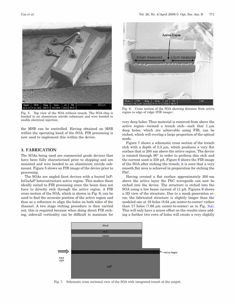
nGaAsP heterostructure active region. This makes themdeally suited to FIB processing since the beam does notave to directly etch through the active region. A FIBross section of the SOA, which is shown in Fig. 6, can besed to find the accurate position of the active region andhus as a reference to align the holes on both sides of thehannel. A two stage etching procedure is then carriedut; this is required because when doing direct FIB etch-ng, sidewall verticality can be difficult to maintain for
ig. 5. Top view of the SOA without trench. The SOA chip isonded to an aluminium nitride submount and wire bonded tonable electrical injection.
Fig. 7. Schematic cross sectional view of
ery deep holes. Thus material is removed from above thective region—termed a trench etch—such that 1 �meep holes, which are achievable using FIB, can betched, which will overlap a large proportion of the opticalode.Figure 7 shows a schematic cross section of the trench
tch with a depth of 2.3 �m, which produces a very flaturface that is 200 nm above the active region. The devices rotated through 90° in order to perform this etch andhe current used is 350 pA. Figure 8 shows the FIB imagef the SOA after etching the trench; it is seen that a verymooth flat area is achieved in preparation for etching thehC.Having created a flat surface approximately 200 nm
bove the active layer the PhC waveguide can now betched into the device. The structure is etched into theOA using a low beam current of 11 pA. Figures 9 shows3D view of the structure. Due to a mask generation er-
or, the fabricated structure is slightly longer than theodeled one at 19 holes (8.64 �m center-to-center) rather
han 17 holes (7.68 �m center-to-center) as in Fig. 1(a).his will only have a minor effect on the results since add-
ng a further two rows of holes will create a very slightly
ig. 6. Cross section of the SOA showing distance from activeegion to edge of ridge (FIB image).
OA with integrated trench at the output.
the S
dof
Passsed39apm
btHm
ltodtltgq
4A1mvmvwi
Fw
FTso
772 J. Opt. Soc. Am. B/Vol. 26, No. 4 /April 2009 Cao et al.
eeper MSB but will have little effect on the MSB positionr bandwidth as seen in the detailed study of length ef-ects in [12].
A critical part of the PhC etching process is placing thehC waveguide symmetrically about the active region,nd a procedure has been developed for this. First, a crossection of the SOA is done, as shown in Fig. 6, in a testample to find the accurate position of the buried hetero-tructure. Then the distance from the active region to thedge of the ridge can be measured as shown. A new SOAevice is then mounted and an alignment mark is placed.8 �m away from the right side of the ridge by using apA beam to show the position of the active region. The
lignment accuracy is estimated to be ±50 nm for thisrocedure. The final etched device showing the alignmentark is shown in Fig. 10.Figure 10 shows that a well defined set of holes have
een etched. An 11 pA beam current is selected to drillhe holes in order to maintain good hole profiles [16].owever the rows of holes closest to the active regionust be etched very carefully such that they do not over-
Fig. 8. Top view of the SOA integrated with the trench.
ig. 9. Schematic 3D view of the SOA with integrated PhCaveguide at the output.
ap with the active region in order to reduce damage tohe quantum wells. In this paper, we designed the widthf the line defect of the PhC waveguide to be 2 �m; futureesigns will be made with wider waveguide cores suchhat the tolerances of the alignment procedure can be re-axed. This will impact the spectral width and position ofhe MSB, and thus a reoptimization of the PhC wave-uide in terms of lattice constant and r /a ratio will be re-uired.
. MEASUREMENTschematic of the measurement setup is shown in Fig.
1. A tunable laser source is used to measure the trans-ission response of the device. Prior to etching, the de-
ices have been measured using a cleaved facet singleode fiber (SMF) to couple light into and out of the de-
ice. Ideally these would be lensed fibers, however, theseere unavailable at the time of measurement; this results
n poor coupling efficiency and thus low gain for the de-
ig. 10. Top view of the SOA with integrated PhC waveguide.he fabricated waveguide is slightly longer than the modeled onehown in Fig. 1(a) at 19 holes long (8.64 �m center-to-center). Allther parameters are the same.
Fig. 11. Schematic of the measurement setup.

vsswpld
td1e[
m=biiwsmpad
v11TSc
a[btalbcwctbiwa
F2
Ft
Fr
Cao et al. Vol. 26, No. 4 /April 2009 /J. Opt. Soc. Am. B 773
ices. The output power is read by the power meter. A la-er diode controller is used to inject current into theample and in combination with a Peltier cooler keeps theorking temperature as required. The measurement iserformed by computer control by connecting the tunableaser, power meter, and temperature controller to theesktop via general-purpose interface bus (GPIB). The
ig. 12. L–I curve of the SOA before FIB etching at 10°C,0°C, and 30°C.
ig. 13. Output power from the SOA with and without trench athe output, where Tmount=20°C and I=200 mA.
ig. 14. Output power from the SOA with PhC waveguide atesonances.
emperature dependence of the L–I curve of an unetchedevice is measured and shown in Fig. 12 in the range of0°C–20°C with Pin=−10 dBm. These curves show thexpected trend of reducing gain at a higher temperature23].
The output power as a function of wavelength was theneasured and is shown in Fig. 13 with I=200 mA, T20°C, and Pin=−10 dBm. It can be seen that no gain iseing obtained due to a poor coupling efficiency. However,n this paper, relative performance before and after etch-ng is the main criterion. The output power of the deviceas then re-measured after etching the trench and is also
hown in Fig. 13. It can be seen that in fact better perfor-ance is being obtained now, but there will be 1–2 dB re-
eatability in these types of measurements due to fiberlignment. The main point to observe is that no majoregradation in performance has occurred.After drilling the holes into the output of SOA, the de-
ice is then remeasured and the results are shown in Fig.4. It can be seen that a distinct “dip” is observed around539 nm, and it is believed that this is an MSB feature.his measured feature is different from the one shown inection 2. This is due to a number of factors as will be dis-ussed later in Section 5.
Tunability of such a notch feature would be very useful,nd tuning of semiconductor optoelectronic devices23,24] and PhCs [25–28] has been investigated by a num-er of workers. To this end measurements have beenaken at two different current levels both with T=20°Cnd Pin=−10 dBm. Figure 14 shows that the notch wave-ength can be tuned over 2 nm for a 100 mA change inias current. The tuning mechanism here is likely to be aarrier induced refractive index change, and this has beenidely used and studied as a tuning mechanism in semi-
onductor devices [24]. Another widely used mechanism isemperature tuning [25] and evidence of such tuning haseen observed in Fig. 15. The amount of tuning observeds consistent with 0.1 nm/C as shown in [25]. Futureork will attempt to optimize the amount of tuningchievable.Unfortunately the MSB feature has a limited lifetime
ifferent bias currents and Tmount=20°C. Inset shows details of
two d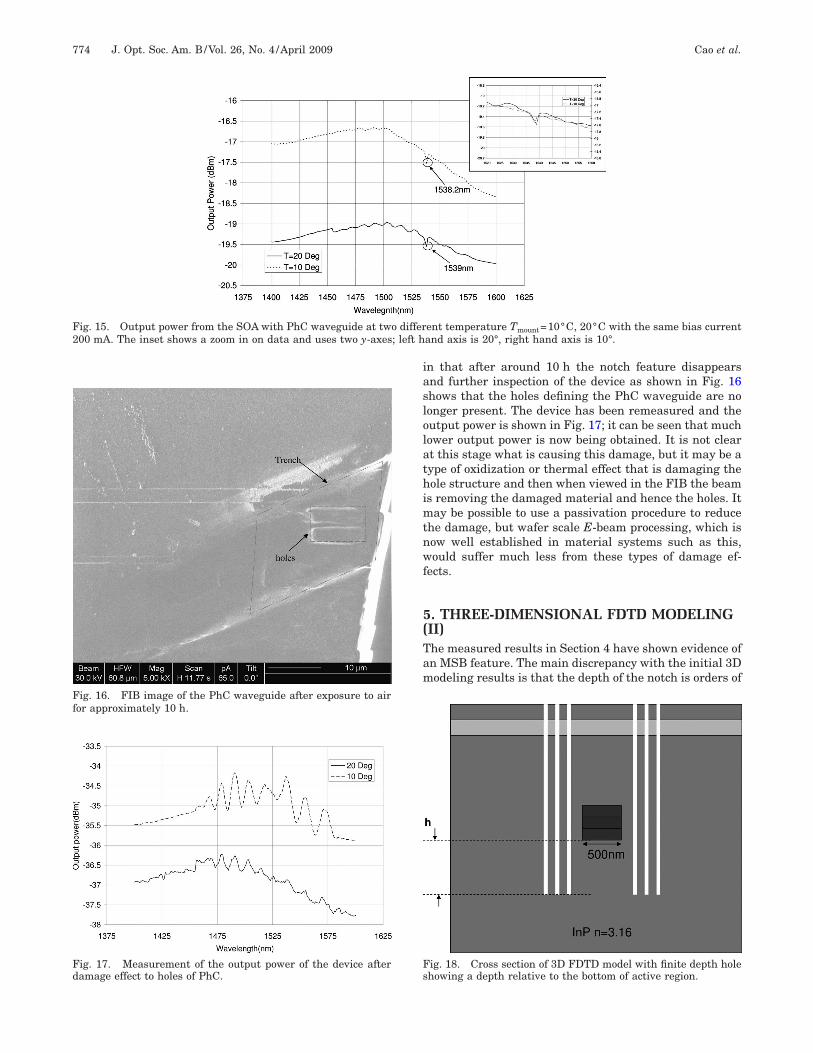
iaslolathimtnwf
5(Tam
F200 mA. The inset shows a zoom in on data and uses two y-axes; left h
Ffor approximately 10 h.
Fd
Fs
774 J. Opt. Soc. Am. B/Vol. 26, No. 4 /April 2009 Cao et al.
n that after around 10 h the notch feature disappearsnd further inspection of the device as shown in Fig. 16hows that the holes defining the PhC waveguide are noonger present. The device has been remeasured and theutput power is shown in Fig. 17; it can be seen that muchower output power is now being obtained. It is not cleart this stage what is causing this damage, but it may be aype of oxidization or thermal effect that is damaging theole structure and then when viewed in the FIB the beam
s removing the damaged material and hence the holes. Itay be possible to use a passivation procedure to reduce
he damage, but wafer scale E-beam processing, which isow well established in material systems such as this,ould suffer much less from these types of damage ef-
ects.
. THREE-DIMENSIONAL FDTD MODELINGII)he measured results in Section 4 have shown evidence ofn MSB feature. The main discrepancy with the initial 3Dodeling results is that the depth of the notch is orders of
ent temperature Tmount=10°C, 20°C with the same bias currentand axis is 20°, right hand axis is 10°.
ig. 18. Cross section of 3D FDTD model with finite depth holehowing a depth relative to the bottom of active region.
ig. 15. Output power from the SOA with PhC waveguide at two differ
ig. 16. FIB image of the PhC waveguide after exposure to air
ig. 17. Measurement of the output power of the device afteramage effect to holes of PhC.

mwsmfi
1b=TM5bdgopi
ebws
M0tbdbatitMbtlf4stle
ttaTosclti
obagwnmf1e
hdsh
Fga
Fg
Fge
Cao et al. Vol. 26, No. 4 /April 2009 /J. Opt. Soc. Am. B 775
agnitude less in the measured case. There is also aavelength shift in the measured results. This section
eeks to improve the agreement by using a more realisticodel for the device. The first feature to be introduced isnite hole depth as shown in Fig. 18.It is believed that the holes are etched approximately�m below the surface of the trench. Thus the depth has
een reduced and two different depths 1 �m �h500 nm� and 1.158 �m �h=658 nm� have been modeled.he results are shown in Fig. 19. It can be seen that theSB has reduced in depth from approximatelyto 2–3 dB. This reduction is caused by light leaking out
eneath the holes as a consequence of the large mode sizeue to the relatively weak confinement in the active re-ion; such effects have been studied in detail by a numberf workers [29,30]. It can also be seen that there is ap-roximately a 0.6 dB reduction in depth of MSB when go-ng from h=0.658 to 500 nm.
The next important feature added to the model is theffect of the air trench that has been shown in Fig. 9. Thisrings air to within 200 nm of the active region and thusill have a large impact on the guided modes. Figure 20
hows the modeled results for this case.These results show two effects; first the depth of theSB is further reduced to 0.7 dB for h=658 nm and
.5 dB for h=500 nm, and the wavelength has shifted tohe region of 1580 nm. The reduction in depth is causedy the presence of the air trench shifting the mode furtherown into the structure resulting in more leakage of lighteneath the holes. This is confirmed when full depth holesre modeled and the depth of the MSB returns to almosthe same level as in Fig. 3. The shift down in wavelengths mainly caused by the presence of air reducing the effec-ive index of the structure producing a reduction in theSB wavelength. The position of the anticrossing in the
and structure that produces the MSB will also be sensi-ive to the geometry of the holes, hence the shift in wave-ength between h=658 and 500 nm. There is a furthereature that the general background loss has increased todB. This is due partly to the fact that there will be more
cattering loss in the transition from the SOA waveguideo the air trench PhC waveguide. However, part of thisoss is also numerical due to the fact that the air trenchxtends to the end of the waveguide into the region where
ig. 19. 3D FDTD model of transmission through PhC wave-uide with finite depth holes for h=500 and 658 nm.
he overlap integrals are calculated. These overlaps refero the fundamental mode of the SOA waveguide, and their trench will therefore introduce an inaccuracy here.he alternative is to not the let the air trench go into theverlap calculation region, however, this will result in acattering loss of a second transition and Fabry–Perot os-illations that are not occurring in the real device. The so-ution to this is to allow overlaps between arbitrary modeso be calculated; it is hoped to implement this in our coden the near future.
These results are now much closer to the measurednes, and the further reduction in depth of the MSB coulde due to the holes being slightly shallower than 1 �mnd the trench being closer than 200 nm to the active re-ion. A slightly deeper trench will also shift the MSBavelength closer to the measured one. Also it should beoted that lossless dielectrics have been used in thisodel; in reality there will be material losses that will af-
ect the MSB depth. The fact that the measured device is9 holes long rather than 17 will only have a very minorffect on the depth and the position of the MSB [12].
The modeling has shown that the fabrication approachere leads to a much reduced MSB depth and mucheeper holes would be needed to obtain the results ashown in Fig. 4. These depths—around 3–4 �m deep—ave been achieved for GaAs and InP based PhC devices
ig. 21. 3D FDTD model of transmission through PhC wave-uide with finite depth, h=658 nm holes and air trench 200 nmbove and below the active region.
ig. 20. 3D FDTD model of transmission through PhC wave-uide with an air trench 200 nm above active region and differ-nt depth holes, h=500 and 658 nm and full depth.

ustTctag
rl5ht
6Tgtssmwtfdtmhtsfsd
ATrtCbta
R
1
1
1
1
1
1
1
1
1
1
2
2
2
2
776 J. Opt. Soc. Am. B/Vol. 26, No. 4 /April 2009 Cao et al.
sing E-beam processing. An alternative route is to con-ider a membrane structure, where an air undercut is in-roduced into the structure beneath the active region.his can also be fabricated using the FIB or E-beam pro-essing using sacrificial layers. The 3D model can be usedo predict the performance of such a device. To this end anir undercut was introduced 200 nm below the active re-ion; the results for this are shown in Fig. 21.
Figure 21 shows that the strong vertical confinementecovers some of the MSB depth; however the scatteringoss at the transition is slightly higher now at around
dB. Tapering will help this to some extent, but it isoped that the gain available in the SOA will be sufficiento offset these losses.
. CONCLUSIONShis paper has presented the integration of a PhC wave-uide into an SOA. The 3D FDTD method has been usedo design an MSB close to 1600 nm, and this has beenhown previously to enable pulse reshaping and compres-ion to be performed. The PhC waveguide is realized byeans of FIB etching, which can achieve 1 �m deep holesith a reasonable hole profile. Experimental data are ob-
ained and the results suggest the existence of an MSBeature; 3D FDTD is then used to include more realisticevice features, such as finite hole depth and the airrench etch, and this shows much better agreement witheasured results than initial modeling. The 3D modeling
ighlights the problem of out-of-plane losses in weak ver-ically confined systems and modeling of a membranetructure shows that a reasonable MSB can be obtainedor this case. In terms of fabrication, annealing and pas-ivation will be investigated in the future to recover theamage induced by the FIB etching.
CKNOWLEDGMENTShis work was funded by the Ultrafast Photonics Collabo-ation (UPC), UK (www.ultrafast-photonics.org). The au-hors would like to thank Joe McGeehan for the use of theondor computing cluster that was donated to Bristol EEy Toshiba Research Labs Europe. They would also like tohank Phil Wade and Patrick Townsend who implementednd maintained the cluster.
EFERENCES1. E. Yablonovitch, “Inhibited spontaneous emission in solid-
state physics and electronics,” Phys. Rev. Lett. 58,2059–2062 (1987).
2. Y. A. Vlasov, M. O’Boyle, H. F. Hamann, and S. J. McNab,“Active control of slow light on a chip with photonic crystalwaveguides,” Nature 438, 65–69 (2005).
3. K. Inoue, and N. Kawai, Y. Sugimoto, N. Carlsson, N.Ikeda, and K. Asakawa, “Observation of small groupvelocity in two-dimensional AlGaAs-based photonic crystalslabs,” Phys. Rev. B 65, 121308 (2002).
4. M. Notomi, K. Yamada, A. Shinya, J. Takahashi, C.Takahashi, and I. Yokohama, “Extremely large group-velocity dispersion of line-defect waveguides in photoniccrystal slabs,” Phys. Rev. Lett. 87, 253902 (2001).
5. V. Berger, “Nonlinear Photonic Crystals,” Phys. Rev. Lett.81, 4136–4139 (1998).
6. J. Li, T. P. White, L. O’Faolain, A. Gomez-Iglesias, and T. F.Krauss, “Systematic design of flat band slow light inphotonic crystal waveguides,” Opt. Express 16, 6227–6232(2008).
7. S. Olivier, M. Rattier, H. Benisty, C. Weisbuch, C. J. M.Smith, R. M De La Rue, T. F. Krauss, U. Oesterle, and R.Houdre, “Mini-stopbands of a one-dimensional system: thechannel waveguide in a two-dimensional photonic crystal,”Phys. Rev. B 63, 113311 (2001).
8. T. Baba, N. Fukaya, and J. Yonekura, “Observation of lighttransmission in photonic crystal waveguides with bends,”Electron. Lett. 35, 654–655 (1999).
9. T. J. Karle, Y. J. Chai, C. N. Morgan, I. H. White, and T. F.Krauss, “Observation of pulse compression in photoniccrystal coupled cavity waveguides,” J. Lightwave Technol.22, 514–520 (2004).
0. T. Cao, M. J. Cryan, P. S. Ivanov, Y-L. D. Ho, G. B. Ren, I. J.Craddock, J. M. Rorison, and C. J. Railton, “Modelling ofchirped pulse propagation through a MSB in a 2D PhCWaveguide,” J. Opt. Soc. Am. B 24, 1575–1583 (2007).
1. T. Cao, M. J. Cryan, I. J. Craddock, J.-Z. Zhang, I.Galbraith, T. Karle, S. Yu, J. Rorison, and C. J. Railton,“Modelling of a 2D photonic crystal waveguide pulsereshaper integrated with a SOA,” in Proceedings of CLEOMunich, Germany, June 12–17, 2005.
2. T. Cao, M. J. Cryan, Y.-L. D Ho, I. J. Craddock, and C. J.Railton, “Fast-light based pulse compression in 2-Dphotonic crystal waveguides,” J. Lightwave Technol. 25,2590–2599 (2007).
3. E. Mizuta, H. Watanabe, and T. Baba, “All semiconductorlow-� photonic crystal waveguide for semiconductor opticalamplifier,” Jpn. J. Appl. Phys., Part 1 45, 6116–6120(2006).
4. E. M Izuta and N. Yokouchi, “Characterization of photoniccrystal waveguide for SOA operation,” in Proceedings ofPacific Rim Conference Laser, and Electro-Optics (2005),paper CThE1-4.
5. L. Giannuzzi and F. Stevie, Introduction to Focused IonBeams Instrumentation, Theory, Techniques, and Practices(Springer, 2005).
6. M. J. Cryan, M. Hill, D. Cortaberria Sanz, P. J. Heard, L.Tian, S. Yu, and J. M. Rorison, “Focused ion beam basedfabrication of nanostructured photonic devices,” IEEE J.Sel. Top. Quantum Electron. 11, 1266–1278 (2005).
7. D. Freeman, C. Grillet, M. W. Lee, C. L. C. Smith, Y. Ruan,A. Rode, M. Krolikowska, S. Tomljenovic-Hanic, C. Martijnde Sterke, M. J. Steel, B. L. Davies, S. Madden, D. J. Moss,Y. H. Lee, and B. J. Eggleton, “Chalcogenide glass photoniccrystals,” Photonics Nanostruct. Fundam. Appl. 6, 3–11(2008).
8. D. Freeman, S. Madden, and B. Luther-Davies,“Fabrication of planar photonic crystals in a chalcogenideglass using a focused ion beam,” Opt. Express 13,3079–3086 (2005).
9. G. Dale, R. M. Langford, P. J. S. Ewen, and C. M. Reeves,“Fabrication of photonic band gap structures in As40S60 byfocused ion beam milling,” J. Non-Cryst. Solids 913,266–269 (2000).
0. M. J. Cryan, R. Varrazza, M. Cowin, M. Hill, I. J. Craddock,S. Yu, C. J. Railton, and J. M. Rorison, “Design, andsimulation of a photonic crystal waveguide filter using theFDTD method,” in Proceedings of LEOS, Glasgow, UK, Nov.5–16, 2002.
1. E. Viasnoff-Schwoob, C. Weisbuch, H. Benisty, C. Cuisin, E.Derouin, O. Drisse, G.-H. Duan, L. Legouézigou, F.Pommereau, S. Golka, H. Heidrich, H. J. Hensel, and K.Janiak, “Compact wavelength monitoring by lateraloutcoupling in wedged photonic crystal multimodewaveguides,” Appl. Phys. Lett. 86, 101107 (2005).
2. S. G. Johnson and J. D. Joannopoulos, “Block-iterativefrequency-domain methods for Maxwell’s equations in aplanewave basis,” Opt. Express 8, 173–190 (2001).
3. T. Kimura, S. Björlin, J. Piprek, and J. E. Bowers, “High-temperature characteristics and tunability of long-wavelength vertical-cavity semiconductor optical

2
2
2
2
2
2
3
Cao et al. Vol. 26, No. 4 /April 2009 /J. Opt. Soc. Am. B 777
amplifiers,” IEEE Photon. Technol. Lett. 15, 1501–1503(2003).
4. B. R. Bennett, R. A. Soref, and J. A. Del Alamo, “Carrier-induced change in refractive GaAs and InGaAsP index ofInP,” IEEE J. Quantum Electron. 26, 113–122 (1990).
5. B. Wild, R. Ferrini, R. Houdré, M. Mulot, S. An, and C. J.M. Smith, “Temperature tuning of the optical properties ofplanar photonic crystal microcavities,” Appl. Phys. Lett. 84,846–848 (2004).
6. H. M. H. Chong and R. M. De La Rue, “Tuning of photoniccrystal waveguide microcavity by thermooptic effect,” IEEEPhoton. Technol. Lett. 16, 1528–1530 (2004).
7. S. W. Leonard, H. M. van Driel, J. Schilling, and R. B.Wehrspohn, “Ultrafast band-edge tuning of a two-dimensional silicon photonic crystal via free-carrierinjection,” Phys. Rev. B 66, 161102 (2002).
8. J. Martz, R. Ferrini, F. Nüesch, L. Zuppiroli, B. Wild, L. A.Dunbar, R. Houdré, M. Mulot, and S. Anand, “Liquidcrystal infiltration of InP-based planar photonic crystals,”J. Appl. Phys. 99, 103105 (2006).
9. H. Benisty, P. H. Lalanne, S. Olivier, M. Rattier, C.Weisbuch, C. J. M. Smith, T. F. Krauss, C. Jouanin, and D.Cassagne, “Finite-depth, and intrinsic losses in verticallyetched two-dimensional photonic crystals,” Opt. QuantumElectron. 34, 205–215 (2002).
0. M. J. Cryan, I. J. Craddock, S. Yu, C. J. Railton, and J. M.Rorison, “Analysis of losses in 2D photonic crystalwaveguides using the 3D finite difference time domain(FDTD) method,” in Proceedings of LEOS Glasgow, UK,Nov. 10–14, 2002.
Copyright © 2022 FDOKUMEN