Terahertz Waveguide Filters Hao Yang - University of ...
197
i Terahertz Waveguide Filters Hao Yang A thesis submitted to the University of Birmingham for the degree of Doctor of Philosophy School of Electronic, Electrical and Systems Engineering The University of Birmingham March, 2019
-
Upload
khangminh22 -
Category
Documents
-
view
3 -
download
0
Transcript of Terahertz Waveguide Filters Hao Yang - University of ...

i
Terahertz Waveguide Filters
Hao Yang
A thesis submitted to the University of Birmingham for the degree of Doctor of
Philosophy
School of Electronic, Electrical and Systems Engineering
The University of Birmingham
March, 2019

University of Birmingham Research Archive
e-theses repository This unpublished thesis/dissertation is copyright of the author and/or third parties. The intellectual property rights of the author or third parties in respect of this work are as defined by The Copyright Designs and Patents Act 1988 or as modified by any successor legislation. Any use made of information contained in this thesis/dissertation must be in accordance with that legislation and must be properly acknowledged. Further distribution or reproduction in any format is prohibited without the permission of the copyright holder.
ii
Abstract
The waveguide filters are popular choices for transmitting and attenuating signals and the
construction of passive circuits. With increasing demands on terahertz systems, waveguide filters
with not only excellent performances but also compact size and lightweight are in need. This thesis
looks into the design of terahertz waveguide filter while taking advantage of specific
micromachining process.
Two waveguide filters operating on WR-3 band (220-325 GHz), one based on high precision
computer numerically controlled (CNC) milling and the other using SU-8 photoresist technology,
are designed and fabricated in this work to achieve demanding specifications. It is the first
demonstration with the best measured performance that a CNC milled filter with a steep rejection
characteristic beyond 300 GHz and a SU-8 micromachined filter with novel cross-coupling
topology working at WR-3 band. These two filters demonstrate potential replacements of
frequency selective surface (FSS) filters used in heterodyne radiometers for unwanted sideband
rejection.
Another two WR-3 waveguide filters based on laser micromachining are also presented in the
thesis. The filter structures are specially chosen to take advantage of the laser cutting processes
and the standard steps of laser micromachining are also optimised accordingly in order to reduce
the fabrication errors and achieve better performances. Although the performance of the two filters
is not perfect, these works show the potential of the laser micromachining for fabricating terahertz
waveguide filters.

iii
Acknowledgement
I would like to thank my supervisor Prof. Mike J. Lancaster for his patient guidance and
continuous support and encouragement during my Ph.D. study in the University of Birmingham.
I am also grateful to my progress report assessor Dr. Alexandros Feresidis for his precious advices.
My appreciation also goes to my colleagues in the Emerging Device Technology Research
Group at the University of Birmingham. In particular, I would like to thank Dr. Xiaobang Shang
for his encouragement and many useful discussions on my work, Dr. Cheng Guo for many
inspiring suggestions and ideas on the filter design, Dr. Yuvaraj Dhayalan and Dr. Pavel Penchev
for fabricating the waveguide filters presented in this thesis. I would also like to thank to Dr. Bo
Liu from University of Glyndwr for the cooperation on the work of optimisation for filters and
diplexers, Dr. Peter G. Huggard and Dr. Hui Wang from Rutherford Appleton Laboratory for the
help on the filter fabrication and measurements.
Finally, I want to express my sincere thanks to my parents and all of my friends for their support
and encouragement.

iv
Table of Contents
Abstract ..................................................................................................................................... ii
Acknowledgement .................................................................................................................. iii
Table of Contents .................................................................................................................... iv
Chater 1 Introduction .............................................................................................................. 1
1.1 Overview of Terahertz Radiation and Applications ................................................................ 1
1.2 Overview of Terahertz Waveguide Circuits and Micromachining ......................................... 2
1.3 Motivations and Objectives .................................................................................................... 4
1.4 Thesis Overview ..................................................................................................................... 5
References ........................................................................................................................................... 7
Chapter 2 General Theory for Resonator Based Filters ...................................................... 9
2.1 Background of Filters Based on Resonators ........................................................................... 9
2.2 Coupling Matrix Representation ............................................................................................. 9
2.3 Physical Realisation of Waveguide Filter ............................................................................. 13
2.3.1 Rectangular waveguide ................................................................................................. 13
2.3.2 Cavity resonator and roupling iris ................................................................................. 15
2.3.3 Determine external quality factor and coupling coefficients ........................................ 18
2.4 Example of a Standard Coupled Resonator Filter ................................................................. 23
2.4.1 Calculation of coupling matrix using specifications ..................................................... 24
2.4.2 Realisation of external quality factors in physical dimensions ..................................... 25
2.4.3 Realisation of coupling coefficients in physical dimensions ........................................ 27
2.4.4 Final optimisation ....................................................................................................... 29
2.5 Conclusions ......................................................................................................................... 31

v
References ....................................................................................................................................... 31
Chapter 3 Micromachining for Terahertz Waveguide Circuit ....................................... 32
3.1 Overview of Micromachining Techniques for Terahertz Waveguide Circuits .......... 33
3.1.1 CNC milling .................................................................................................................. 33
3.1.2 Si deep reactive ion etching (DRIE) ............................................................................. 36
3.1.3 LIGA process ................................................................................................................ 39
3.1.4 SU-8 photoresist technology for micromachining ........................................................ 41
3.1.5 Laser micromachining ................................................................................................... 42
3.1.6 3-D printing ................................................................................................................... 45
3.2 Fabrication Process for SU-8 photoresist technology ........................................................... 46
3.3 Conclusions ........................................................................................................................... 53
References ......................................................................................................................................... 56
Chapter 4: Micromachined Waveguide Circuits Using High Precision CNC Machining and
SU-8 Photoresist Technology ................................................................................................ 62
4.1 Background ........................................................................................................................... 63
4.2 Design of the Waveguide Filters ...................................................................................... 65
4.3 CNC Milled Extracted Pole filter .......................................................................................... 69
4.3.1 Design process of extracted pole filter .......................................................................... 69
4.3.2 Fabrication and measurement details for CNC milled filter ......................................... 73
4.3.3 Difference analysis ........................................................................................................ 77
4.4 SU-8 Micromachined Filter .................................................................................................. 78
4.4.1 Design process of SU-8 micromachined filter .............................................................. 78
4.4.2 Fabrication and measurement details for for SU-8 micromachined filter ..................... 82
4.4.3 Difference analysis ........................................................................................................ 87

vi
4.5 Comparison and Discussion .................................................................................................. 89
References ......................................................................................................................................... 93
Chapter 5: Micromachined Waveguide Circuits Fabricated by Laser ............................ 97
5.1 Background ........................................................................................................................... 97
5.2 Laser Machined Double Layer Filter .................................................................................. 100
5.2.1 Design process of double layer filter .......................................................................... 100
5.2.2 Fabrication details ....................................................................................................... 103
5.2.3 Measurement results and discussion ........................................................................... 106
5.3 Laser Machined Filter with Bends ...................................................................................... 112
5.3.1 Design process of filter with two H-bends .................................................................. 112
5.3.2 Measurement and discussion ...................................................................................... 117
5.3.3 Improvements for the process ..................................................................................... 123
5.4 Conclusions ......................................................................................................................... 128
References ....................................................................................................................................... 130
Chapter 6: Conclusions and Further Work ...................................................................... 132
5.1 Conclusions ......................................................................................................................... 132
5.2 Future Work ........................................................................................................................ 135
References ....................................................................................................................................... 137
Appendix I: Optimisation for Filters and Diplexers ......................................................... 138
Appendix II: Publications ................................................................................................... 155

1
Chapter 1
Introduction
1.1 Overview of Terahertz Radiation and Applications
Terahertz radiations are electromagnetic waves with a frequency range from about 0.1 THz to
10 THz, or wavelengths between 3 mm and 30 μm, which lie between the microwave and infrared
regions of the spectrum [1]. Terahertz frequency range is also the last span within the whole
electromagnetic wave spectrum, which has rarely been technologically and commercially
developed. From the literature, the terahertz frequency range is often referred to as ‘terahertz gap’
due to this reason. Meanwhile, this frequency range presents incredibly fascinating prospects for
many applications [2].
Terahertz radiation mainly exhibits three attractive properties for applications. The first
property is that terahertz radiations are non-ionizing, able to pass through dielectrics such as paper,
plastic, cloth and wood, with little attenuation, while metals are highly reflective in this frequency
region. Many materials which block visible and infrared (IR) spectra, appear to be transparent in
the terahertz region. As compared to microwave radiation, employing terahertz frequency range is
able to achieve better spatial resolution required for rendering quality imaging [3]. The next unique
property is that terahertz radiations are safe for biological entities due to its relatively low energy.
As compared to X-rays which have the risk of creating ionization in biological tissues, terahertz
waves have absolutely no ionizing radiation impact, presenting no health hazard to humans and
animals being scanned. The third special property is that many substances reveal their unique
spectral fingerprints in the far terahertz range (1 - 3 THz), which provides unique information
about their structure and allows conducting their chemical analysis [3].

2
Because of these properties, terahertz radiation has promising applications in areas such as
safety monitoring imaging. As introduced preciously, normal covering or packing material (i.e.
cloth) are transparent to terahertz radiations while liquid explosives or drugs can be distinguished
from their unique spectral characteristics. Metal objects are opaque in the image since they reflect
all terahertz radiations. The advantages of low energy, high signal to noise ratio and high
sensitivity to the water content in biological tissues [3] present great potential of employing
terahertz radiation in medical imaging. As for high frequency communication systems, compared
to microwave frequencies, terahertz frequency carriers enable lager available bandwidth as well
as smaller size for terahertz components. However, in practice the terahertz radiation suffer from
large atmospheric attenuation and can’t propagate for long distance in earth’s atmosphere. In spite
of this drawback, terahertz radiation presents its great potential applications in other area such as
quality control, non-destructive testing, astronomy, atmospheric research, short distance wireless
communications, networking and military applications [3]. During the last few decades, many
studies and researches have been carried out in order to fill the ‘terahertz gap’, yet not so many
really successful breakthroughs have been made, but the unique properties of terahertz sicence and
technology suggest that its applications will grow fast [3].
1.2 Overview of Terahertz Waveguide Circuits and Micromachining
Waveguide is one kind of transmission line (usually in the form of a rectangular tube) for the
propagation of electromagnetic waves. Compared with other typical transmission lines operating
at same frequencies (i.e. microstrip, coaxial cable), waveguide can provide the lowest loss and best
power handling capacity [4]. For microwave frequency applications, the bulky size of waveguide

3
circuits becomes the main drawback. Fortunately, for waveguide components in general, device
dimensions decrease as frequency increases. As the operating frequencies of the waveguides go
up into terahertz region, the waveguide components become smaller which means the size of
waveguide is no longer a drawback. In this case, for terahertz circuits, rectangular waveguide is
an ideal low loss medium for interconnectivity and for the construction of passive circuits [4].
However, new challenge comes as tighter dimensional accuracy is required for the fabrication of
terahertz waveguide. For example, the cross-sectional dimensions for a WR-3 band (220 - 325
GHz) waveguide is just 864 by 432 µm, and the dimensions of the additional structures inside the
waveguide (for example for a filter) can be much smaller than the dimensions of the waveguide
itself. The dimensional accuracy required for a waveguide filter based on coupled resonators is
even more demanding since the performance of the circuit is very sensitive to the dimensional
sizes such as the length of the resonators and width of the coupling iris. From this perspective,
more and more researchers have looked into different micromachining techniques to accomplish
complex waveguide features with high dimensional accuracy.
Computer Numerical Control (CNC) machining is a traditional way of fabricating metal
waveguide components and has been recently utilised for manufacturing devices operating at low
terahertz frequencies (0.1-0.3 THz). Waveguide components fabricated by CNC milling with
excellent performance have been reported in [5] and [6]. However, researchers are pushing the
limit of the CNC micromachining. The structures of the waveguide filter are carefully designed to
be achievable by CNC milling process. With the development of high precision CNC machines,
CNC milling process remains a good choice for fabricating components operating at terahertz
frequencies.
Other alternative micromachining process such as silicon deep reactive ion etching (DRIE) [7-

4
9], lithographic micromachining technique (LIGA) [10] and SU-8 photoresist technology [11-13],
have been developed and employed by the researchers to achieve high-dimensional accuracy in
the fabrication of terahertz waveguide filters. In [14], laser micromachining and 3-D printing have
also been utilised for waveguide filters using different designs at about 100 GHz. These
micromachining processes have shown great potential for the fabrication of terahertz waveguide
circuits. However, each micromachining process has its advantages and drawbacks. This will be
discussed in Chapter 3 with more details.
1.3 Motivations and Objectives
There has been great potential for the exploiting of terahertz frequency range due to its
promising scientific and industrial applications. Many of the existing terahertz instruments are
typically very large, difficult to use, intended for specific narrow applications, and prohibitively
expensive. The work presented in this thesis focus on reducing the size, weight and cost of terahertz
circuit while maintaining its quality of performance. For terahertz systems, the waveguide circuits
have become a popular choice of transmission line, due to its lower loss and better power handling
capacity. However, the responses of waveguide circuits operating at terahertz frequencies are
especially sensitive to the dimensional accuracy, which brings challenges for the fabrication
techniques of micro-structures.
Many manufacturing methods have been proposed and modified by the researchers to deal with
the fabrication of complex waveguide circuits working at high frequencies. techniques as well as
present a number of terahertz waveguide filters showing the advantages of micromachining
technologies at terahertz frequencies. The main objectives of this thesis are (1) compare different

5
micromachining techniques and choose the most suitable processes based on potential
performances, costs and available resources; (2) design and fabricate a number of terahertz
waveguide filters which take advantage of the fabrication process while pushing the limits of state-
of-art for the micromachining process (i.e. SU-8 photoresist technology and laser micromachining
in this work).
1.4 Thesis Overview
This thesis is in two major parts: (i) a general review of waveguide filter design techniques and
micromachining for terahertz waveguide circuits; (ii) terahertz waveguide circuits based on CNC
milling, SU-8 photoresist technology and laser micromachining. Chapters 2-3 focus on the first
part and Chapters 4-5 present the latter.
Chapter 1 gives the overview of terahertz radiation and its application, an overview of terahertz
waveguide circuits and micromachining, together with the motivations and objectives for the thesis.
An overview of the structure for this thesis is also included in this part.
Chapter 2 is intended to provide the general theories which are used to design waveguide filters
presented in this thesis. The overview of coupled resonator filters and its coupling matrix
representation is presented. This is followed by the overview of the waveguide filter technology
and its physical realisation. In the last part of this chapter, a filter design example is given.
Chapter 3 reviews the micromachining techniques for the fabrication of terahertz waveguide
circuits (mainly waveguide filters). The process and applications for CNC milling, DRIE process,
LIGA process, SU-8 photoresist technology, laser micromachining and 3D-printing are introduced.
This is followed by the discussion of the advantages and disadvantages of each process in each

6
subsection. Then the SU-8 micromachining process, which is developed at University of
Birmingham (EDT group) and employed in the filter presented in Chapter 4; it is explained in
detail. In the last part, a comparison of these micromachining techniques is provided.
Chapter 4 mainly presents the designs, fabrication and measurements of two micromachined
circuits working at WR-3 band (220-325 GHz). One is based high precision CNC machining and
another is fabricated using SU-8 photoresist technology. The specification is provided in the first
part, followed by the discussion of filter design process. Then the fabrication, measurement and
analysis of measured responses are presented. At the end of this chapter, the comparison of these
two filters, together with other recently published waveguide filter operating in frequency from
WR-10 to WR-1.5 band is given.
Chapter 5 deals with two laser micromachined waveguide filters both composed of four coupled
resonators operating in TE101 mode working at WR-3 band. The first one uses a novel double-layer
design and the second is designed with two H-bends. The design methods, an improved fabrication
process of laser cutting and the measurements for both filters are discussed in detail in this chapter.
Difference analysis between measured results and designed responses, and further suggestions for
employing laser micromachining are presented in the last part of this chapter.
Chapter 6 is the conclusion of the whole thesis. The first part summaries the work that has been
done and the main novelties for this work. The second part presents the comparisons between
filters described in Chapter 4 and 5. The comparisons contain the measurement responses as well
as the discussion of further applications of these processes. The suggestions for future work are
also included in this chapter.
7
References:
[1] J. Hu, S. Liu, Y. Zhang and R. Xu, “Micromachined terahertz waveguide band-pass
filters,” 2017 IEEE MTT-S International Microwave Symposium (IMS), Honololu, HI, pp. 650-
653, 2017
[2] X. Shang, “SU-8 Micromachined Terahertz Waveguide Circuits and Coupling Matrix Design
of Multiple Passband Filters,” Ph.D. dissertation, School Electron., Elect. Syst. Eng., Univ.
Birmingham, Birmingham, U.K., 2011.
[3] A. Redo-Sanchez and X. C. Zhang, “Terahertz Science and Technology Trends,” IEEE Journal
of Selected Topics in Quantum Electronics, vol. 14, no. 2, pp. 260-269, Mar. 2008.
[4] H. Yang, Y. Dhayalan, X. Shang, M. J. Lancaster, et al, “WR-3 waveguide filter based on high
precision CNC milling and SU-8 photoresist technology,” IEEE Trans. THz Sci. Technol, vol. 8,
no. 1, pp. 100-107, Jan. 2018.
[5] C. A. Leal-Sevillano, J. R. Montejo-Garai, J. A. Ruiz-Cruz and J. M. Rebollar, “Low-Loss
Elliptical Response Filter at 100 GHz,” IEEE Microw. Wireless Compon. Lett., vol. 22, no. 9, pp.
459-461, Sep. 2012.
[6] J. Q. Ding, S. C. Shi, K. Zhou, Y. Zhao, D. Liu and W. Wu, “WR-3 Band Quasi-Elliptical
Waveguide Filters Using Higher Order Mode Resonances,” IEEE Trans. THz Sci. Technol., vol.
7, no. 3, pp. 302-309, May. 2017.
[7] H. V. Jansen, M. J. de Boer, S. Unnikrishnan, M. C. Louwerse and M. C. Elwenspoek, “Black
silicon method X: a review on high speed and selective plasma etching of silicon with profile
control: an in-depth comparison between Bosch and cryostat DRIE processes as a roadmap to next
generation equipment,” Journal of Micromechanics and Microengineering, IOP Publishing, Ltd,

8
Feb. 2009.
[8] J. Y. Li, B. Pan, C. Lugo, M. Tentzeris, and J. Papapolymerou, “Design and characterization
of aW-band micromachined cavity filter including a novel integrated transition from CPW feeding
lines,” IEEE Trans. Microw. Theory Tech., vol. 55, no. 12, pp. 2902–2910, Dec. 2007.
[9] K. M. K. H. Leong et al., "WR1.5 Silicon Micromachined Waveguide Components and Active
Circuit Integration Methodology,” IEEE Trans. Microw. Theory Tech., vol. 60, no. 4, pp. 998-
1005, Apr. 2012.
[10] J. R. Stanec and N. S. Barker, “Fabrication and integration of micromachined submillimeter-
wave circuits,” IEEE Microw. Wireless Compon. Lett., vol. 21, no. 8, pp. 409–411, Aug. 2011.
[11] X. Shang, M. Ke, Y. Wang and M. J. Lancaster, “Micromachined W-band waveguide and
filter with two embedded H-plane bends,” IET Microw., Antennas Propag., vol. 5, no. 3, pp. 334-
339, Feb. 2011.
[12] Q. Chen, X. Shang, Y. Tian, J. Xu and M. J. Lancaster, "SU-8 micromachined WR-3 band
waveguide bandpass filter with low insertion loss," Electron Lett., vol. 49, no. 7, pp. 480-482,
March. 2013.
[13] X. Shang, Y. Tian, M. J. Lancaster, S. Singh, “A SU8 micromachined WR-1.5 band
waveguide filter,” IEEE Microw. Wireless Compon. Lett., vol. 23, (6), pp. 300-302, Jun. 2013
[14] X. Shang et al., “W-Band Waveguide Filters Fabricated by Laser Micromachining and 3-D
Printing,” IEEE Trans. Microw. Theory Tech., vol. 64, no. 8, pp. 2572-2580, Aug. 2016.

9
Chapter 2
General Theory for Resonator Based Filters
2.1 Background of Filters Based on Resonators
A filter is a two-port network commonly utilised for transmitting or attenuating signals for
desired frequency bands. The coupled resonator filter is a common type of filter and has been
presented in literature for applications in communication system and radar systems [1].
A general synthesis for design filters using coupled resonators can be found in [2]. This
technique can be utilised to any kinds of resonators regardless of their physical geometry. Using
coupling matrix to represent filter circuits is the key process in such a technique. By modelling the
filter in a matrix, each physical element of the final filter circuit can be transferred to a
corresponding element in the coupling matrix [3]. Before the introduction of the terahertz filters,
the basic knowledge for coupled resonator filter theory related to this work are presented in this
chapter.
2.2 Coupling Matrix Representation
The derivation of the representation of general coupling matrix for a coupled resonator filter
has been introduced in [2]. The equivalent circuit with magnetically coupled resonators and circuit
with electrically coupled resonators are given in Fig. 2.1 (a) and (b) respectively. In Fig. 2.1, R, G,
C and L represent the resistance, conductance, capacitance and inductance; i and v stand for the
current and voltage.

10
Fig. 2.1 Equivalent circuit of a waveguide filter composed of (a) magnetically n-coupled resonators (b)
electrically n-coupled resonators [2].
By employing Kirchoff’s voltage and Kirchoff’s current law, the coupling matrix can be derived
from an impedance matrix using a set of loop equations or via an admittance matrix calculated
using a set of node equations [2]. The derivations present that the normalised admittance matrix
and normalised impedance matrix have identical form. We will not reproduce the derivation here,
however the result for a general matrix [A] in terms of coupling coefficients and external quality
factors for both kinds of coupling introduced above is [2]:

11
1,1 1,2 1,1
2,1 2,2 2,
,1 ,2 ,
10 0
1 0 0
0 0 0 0 1 0
1 0 0 10 0
ne
n
n n n n
en
m m mq
m m mA q p U j m p j
m m m
q
= + − = + −
(2.1)
0
0
1p j
FBW
= −
(2.2)
where qei is the normalised external quality factor of resonator i, [q] is the n n matrix with all
entries zero, except for 11 11/ eq q= and 1/nn enq q= , matrix [U] is the n n unit matrix, p is
the complex low pass frequency variable, 0 is the centre frequency of the resonator, FBW
represents the fractional bandwidth for the waveguide filter. mij ( )i j is the normalised coupling
coefficient between the resonator i and j, the diagonal entries mii is the self-coupling coefficient.
As presented in [2], the insertion loss and return loss (S-parameters) of this coupled resonator
filter can be calculated using the general matrix [A] with normalised external quality factors as:
1
11 1,11
1
21 ,11
21
12
e
ne en
S Aq
S Aq q
−
−
= −
=
(2.3)
For filters with Chebyshev, Butterworth and Elliptic or other standard responses, the normalised
external quality factors and general coupling matrix [A] can be calculated from its low-pass
prototype elements g0, g1, …gn+1, which can be found from tables directly or calculated by
formulas shown in equation (2.4) [2].

12
The low-pass prototype g values for the Chebyshev filter with a passband ripple LAr dB and the
cut-off frequency 1c = are calculated using the following formulas given in [2],
0
1
2 21
1 2
1
2sin
2
(2 1) (2 3)4sin sin
1 2 2( 2 to )
( 1)sin
1 for odd
coth for even4
i
i
n
g
gn
i i
n ng i n
ig
n
n
gn
−
+
=
=
− −
= =
− +
=
(2.4)
where
ln coth17.37
sinh2
ArL
n
=
=
Using lumped elements, the normalised external quality factors and the coupling coefficients
between adjacent resonators for Chebyshev lowpass prototype filters can be calculated from g
values as:
1 0 1 1
, 1
1
,
1 for 1 to 1
e en n n
i i
i i
q g g q g g
m i ng g
+
+
+
= =
= = − (2.5)

13
2.3 Physical Realisation of Waveguide Filter
2.3.1 Rectangular waveguide
x
y
z
ab
Fig. 2.2 Cross section of a rectangular waveguide [4]
The design of a waveguide filter will be discussed in Section 2.3.4. However, before proceeding
this we will discuss the basic principles of a rectangular waveguide as it is so important for the
work in this thesis. A waveguide is performed as a circuit which directs the propagation of energy
in the form of an electromagnetic wave [4]. The rectangular waveguide, of which the cross section
is shown in Fig.2.2, is the most common type of waveguide [4]. The following presents several
important properties of a rectangular waveguide. More detailed descriptions of waveguide theory
can be found in [4].
In a rectangular waveguide, TE (i.e. transverse electric) and TM (i.e. transverse magnetic)
modes are allowed to propagate while a TEM (i.e. transverse electromagnetic) mode is not
supported. The cut-off frequency is defined as the lowest frequency each mode can propagate
through the waveguide. From the derivation in [4], the cut-off frequency fcutoff of each TEmn mode
of TMmn mode is calculated as equation (2.6).

14
2 2( ) ( )
2cutoff
c m nf
a b= + (2.6)
where a and b represent the width and height of the rectangular waveguide, c is the speed of light
in free space, m and n are the number of half standing waves along the width (x axis) and height
(y axis) of the rectangular waveguide. The mode with the lowest cut-off frequency is called the
dominant mode. For common rectangular waveguide which meets the condition of a=2b, the TE10
mode is the dominant mode as it has the lowest cut-off frequency of 10
/ 2cutoffTEf c a= . As for TE20
mode, it has the second lowest cut-off frequency of 20
/cutoffTEf c a= . In this situation (a=2b), in the
frequency band between c/2a and c/a only the TE10 mode propagate inside the waveguide, so when
using this frequency band, the waveguide is said to be as single mode, the useful bandwidth of this
rectangular waveguide is calculated as 20 10
/ 2cutoffTE cutoffTEf f c a− = . To get rid of the influence of
higher modes, rectangular waveguides are almost always operated in the band in which they are
single-mode [4]. In this case, when designing waveguide filters, the passband of the filter should
also be designed within the single-mode frequency band for such waveguide.
For non-standard rectangular waveguide, for example, for b ˃ a/2, the cut-off frequency of the
TE01 mode would be calculated as the second-lowest based on equation (2.6). The actual useful
bandwidth of the rectangular waveguide is calculated as 01 10
/ /cutoffTE cutoffTEf f c b c a− = − , which
has relatively smaller single mode bandwidth. Therefore, in order to obtain wider useful bandwidth,
b is preferred to be no bigger than a/2. However, the waveguide attenuation increases as b increase
[4]. For rectangular waveguide of b˂ a/2, the useful bandwidth is still between the cut-off of TE10
mode and TE20 mode, however the attenuation would increase [4]. Therefore, for a rectangular

15
waveguide, the optimum height b is exactly half of the width a.
2.3.2 Cavity resonator and coupling iris
Fig. 2.3 A standard rectangular cavity resonator
Cavity resonators are able to store both electric and magnetic energy [3] and they are the key
components in the physical realization of a resonator filter. A cavity resonator is composed by
rectangular waveguide ended with two conducting walls at both ends [3]. A standard single cavity
resonator is shown in Fig. 2.3. The resonant frequency and the unloaded quality factor are two
important parameters for a cavity resonator. The calculation of resonator frequency and unloaded
quality factor of a single cavity resonator using the physical dimensions is presented in the
following part.
The resonant frequency is the frequency at which the stored electric energy within a single
cavity equals the stored magnetic energy [3]. For a rectangular waveguide cavity, the transverse

16
electric field (Ex, Ey) of the TEmn or TMmn mode can be express as [4]:
( , , ) ( , )[ ]z zmn mn
j j
tE x y z e x y A e A e − −+ −= + (2.7)
In the above equation (2.7), ( , )e x y represents the transverse variations in the x and y directions,
A+ and A− represent the amplitude of the travelling wave in +z and -z (forward and backward)
directions. mn is defined as the propagation constant for the TEmn or TMmn mode and can be
found in [4] as:
2 2 2( ) ( )mn
m nk
a b
= − − (2.8)
where k is the wavenumber which can be calculated as 02k f = , is the permeability and
is the permittivity of the material within the waveguide [4]. From equation (2.7), by employing
the condition that ( , ,0) 0tE x y = and ( , , ) 0tE x y d = , we can get:
1,2,32
g
r
mn
l l l for l
= = = (2.9)
Equation (2.9) indicates that the length of a cavity resonator lr should be integer l times of half
guided wavelength g of the considered mode at the resonant frequency [4]. The cut-off
wavenumber of the rectangular cavity resonator can be calculated as [4]:
2 2 2( ) ( ) ( )mnl
m n lk
a b d
= + + (2.10)
where the m, n and l represent the number of half wavelength variations in the x, y, z directions,

17
respectively. Then the modes existing in the cavity resonator can be expressed as TEmnl and TMmnl,
while the resonator frequency fmnl of these modes can be calculated as:
2 2 2( ) ( ) ( )2 2
mnlmnl
r r r r
ck c m n lf
a b d
= = + + (2.11)
where c is the speed of light in free space, r and r stand for the relative permeability and
permittivity of the material filling the waveguide, respectively.
The unloaded quality factor Qul is used to describe the inherent loss in a resonator and is defined
as the ratio between the energy stored in the resonator versus power lost per unit time [3]. A
low/high unloaded quality factor corresponds to a high/low loss. The unloaded quality factor for a
single cavity resonator is calculated using equation (2.12).
11 1
( )c
ul
d
QQQ
−= + (2.12)
where Qc stands for the factor of loss caused by lossy conducting walls and Qd represents the loss
caused by dielectric that is filling in the resonator. For the filters designed in this work, air is the
filling material within the resonator, therefore dQ → . In this case, only Qc is considered and
used to calculated the unloaded quality factor. From [1], the Qc of a single cavity resonator working
at TE10l mode is calculated as:
3
2 3 3 3 3
( )
2 (2 2 )c
s
kad bQ
R a b bd a d ad
=
+ + + (2.13)
where Rs is the surface resistance, the conductivity of the conductive wall for the resonator is ,
Rs is then calculated as / 2sR = [1]. η is the wave impedance and calculated as
18
/ = .
In a waveguide filter design, the cavity resonators are typically coupled by inductive iris or
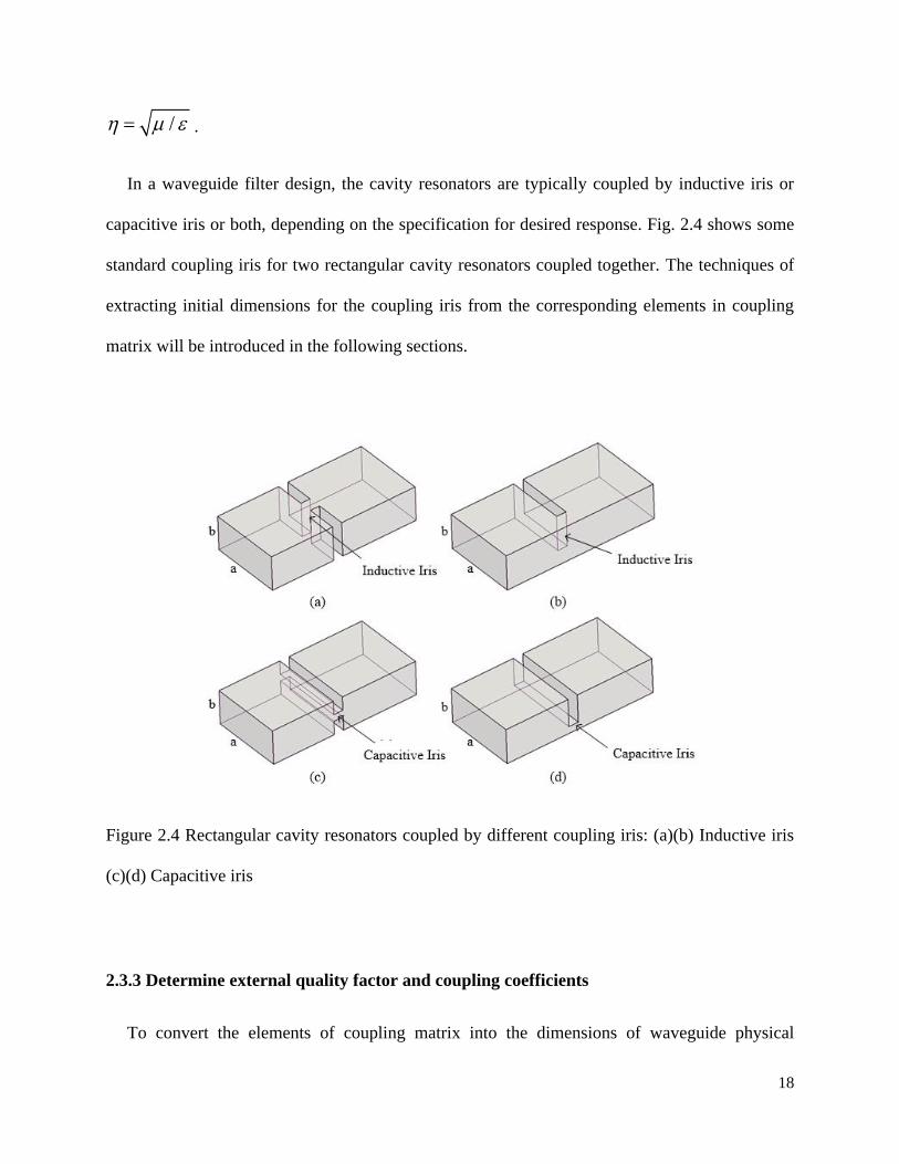
capacitive iris or both, depending on the specification for desired response. Fig. 2.4 shows some
standard coupling iris for two rectangular cavity resonators coupled together. The techniques of
extracting initial dimensions for the coupling iris from the corresponding elements in coupling
matrix will be introduced in the following sections.
Figure 2.4 Rectangular cavity resonators coupled by different coupling iris: (a)(b) Inductive iris
(c)(d) Capacitive iris
2.3.3 Determine external quality factor and coupling coefficients
To convert the elements of coupling matrix into the dimensions of waveguide physical

19
structures, it is important to figure out the relationship between each matrix entry and its related
physical dimension for the waveguide components. As described above, the external quality
factors and internal coupling coefficients between resonators can be derived from the filter’s
specifications. Then the physical dimensions of the filter structures can be determined using the
following techniques [1].
The definition of unloaded quality factor Qul is described in Section 2.3.2. For the cavity
coupled with a source and load, the loaded quality factor Ql is calculated as:
11 1
( )ul
l
e
QQ Q
−= + (2.14)
where Qe is the external quality factor.
Fig. 2.5 Single resonator cavity externally coupled to one port and weakly coupled to another port
The loaded quality factor can be measured by simulation S21 response of the single cavity
resonator with one port externally coupled to input port and another port weakly coupled to output

20
port. Fig. 2.5 shows an example of a resonator cavity that is externally coupled to the input port
and weakly coupled to the output port. From the simulated S21 response shown in Fig. 2.6, the
loaded quality factor Ql is calculated in equation (2.15) using the resonator frequency f0 and the 3-
dB bandwidth 3-dBf as:
0
3-
l
dB
fQ
f= (2.15)
Fig. 2.6 3-dB bandwidth in simulated S21 response (Figure reproduced form [3])
It should be noted that Ql should be calculated when f0 is equal to resonant frequency of the
cavity, otherwise the length l of the resonator should be adjusted to make f0 equal to the desired
resonant frequency. For perfect electric conductor and no radiation to the environment the EM

21
simulator (i.e. CST Microwave Studio) then the unloaded quality factor ulQ → . From equation
(2.7) the external quality factor Qe can be calculated as:
leQ Q= (2.16)
To determine the internal coupling coefficient kc (this is corresponded to mij in the coupling
matrix), the structure shown in Fig. 2.7 is given. The two resonators are identical and internally
coupled to each other. The other port of each filter is weakly coupled to input/output port.
Fig. 2.7 Two coupled resonators with weak external couplings to input/output ports.

22
Fig. 2.8 Simulate results of S11 and S21 for two coupled resonators
Figure 2.8 shows the simulated S21 of the two coupled resonators. 1f and 2f are the frequencies
of two peaks of simulated S21. The coupling coefficient between each two resonators kc can be
calculated from the formulation as [5]:
222 22 2
02 01 02 012 1
2 2 2 2
01 02 2 1 02 01
1
2c
f f f ff fk
f f f f f f
−−= + −
+ +
(2.17)
where, 01f and 02f are the resonant frequencies of each uncoupled resonator.
When the coupled resonators are synchronously tuned (i.e. 01 02f f= ), equation (2.17) is
simplified as [2]:
2 2
2 1
2 2
2 1
c
f fk
f f
−=
+ (2.18)
For asynchronously tuned resonators, when the ratio of two resonant frequencies f01 and f02 is
within a small range ( 01 02 02 01/ 1.1, f f f f ), the asynchronously tuning has very little effect

23
on the value of the internal coupling coefficient [3]. The topology in Fig. 2.7 can also be applied
to extract the internal coupling of the asynchronously tuned resonators. However, for more
complicated situations (e.g. 01 02 02 01/ 1.1, f f f f ), we need to apply the full equation of
(2.17) to calculate the coupling coefficient between two resonators.
The above techniques give the initial values for the dimensions of the filter design, by
connecting resonators in series, the coupled resonator filter is formed. After optimisation process
in EM simulators, the response can be optimised to match the filter specification.
2.4 Example of a Standard Coupled Resonator Filter
From the filter’s specification, the external quality factors and coupling coefficients between
resonators can be obtained in a coupling matrix. The physical dimensions can be extracted from
the corresponding elements in the coupling matrix using the method explained in section 2.3.3.
Here, the design of a 3rd order Chebyshev filter centred at 300 GHz with 5% fractional bandwidth
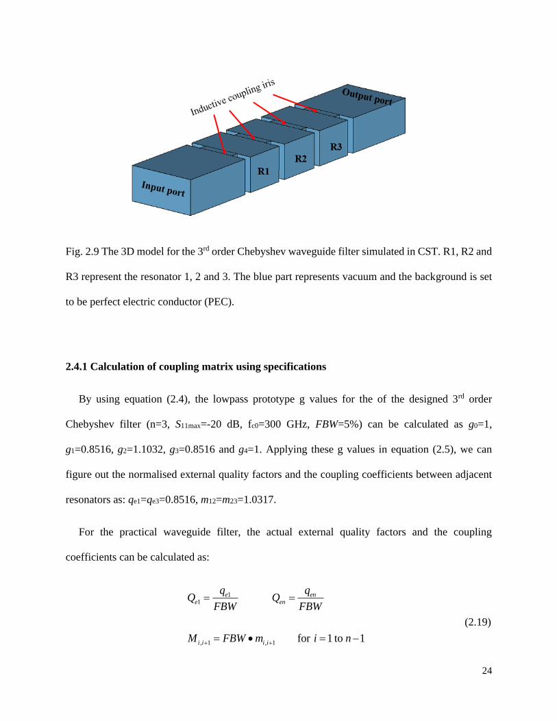
and 20 dB maximum return loss within passband is presented as an example. As shown in Fig. 2.9,
the waveguide filter is composed of three cavity resonators working in the TE101 mode. Both the
external couplings with input/output port and the internal couplings between resonators are
realised by symmetric inductive iris in this example.
24
Fig. 2.9 The 3D model for the 3rd order Chebyshev waveguide filter simulated in CST. R1, R2 and
R3 represent the resonator 1, 2 and 3. The blue part represents vacuum and the background is set
to be perfect electric conductor (PEC).
2.4.1 Calculation of coupling matrix using specifications
By using equation (2.4), the lowpass prototype g values for the of the designed 3rd order
Chebyshev filter (n=3, S11max=-20 dB, fc0=300 GHz, FBW=5%) can be calculated as g0=1,
g1=0.8516, g2=1.1032, g3=0.8516 and g4=1. Applying these g values in equation (2.5), we can
figure out the normalised external quality factors and the coupling coefficients between adjacent
resonators as: qe1=qe3=0.8516, m12=m23=1.0317.
For the practical waveguide filter, the actual external quality factors and the coupling
coefficients can be calculated as:
11
, 1 , 1 for 1 to 1
e ene en
i i i i
q qQ Q
FBW FBW
M FBW m i n+ +
= =
= • = −
(2.19)
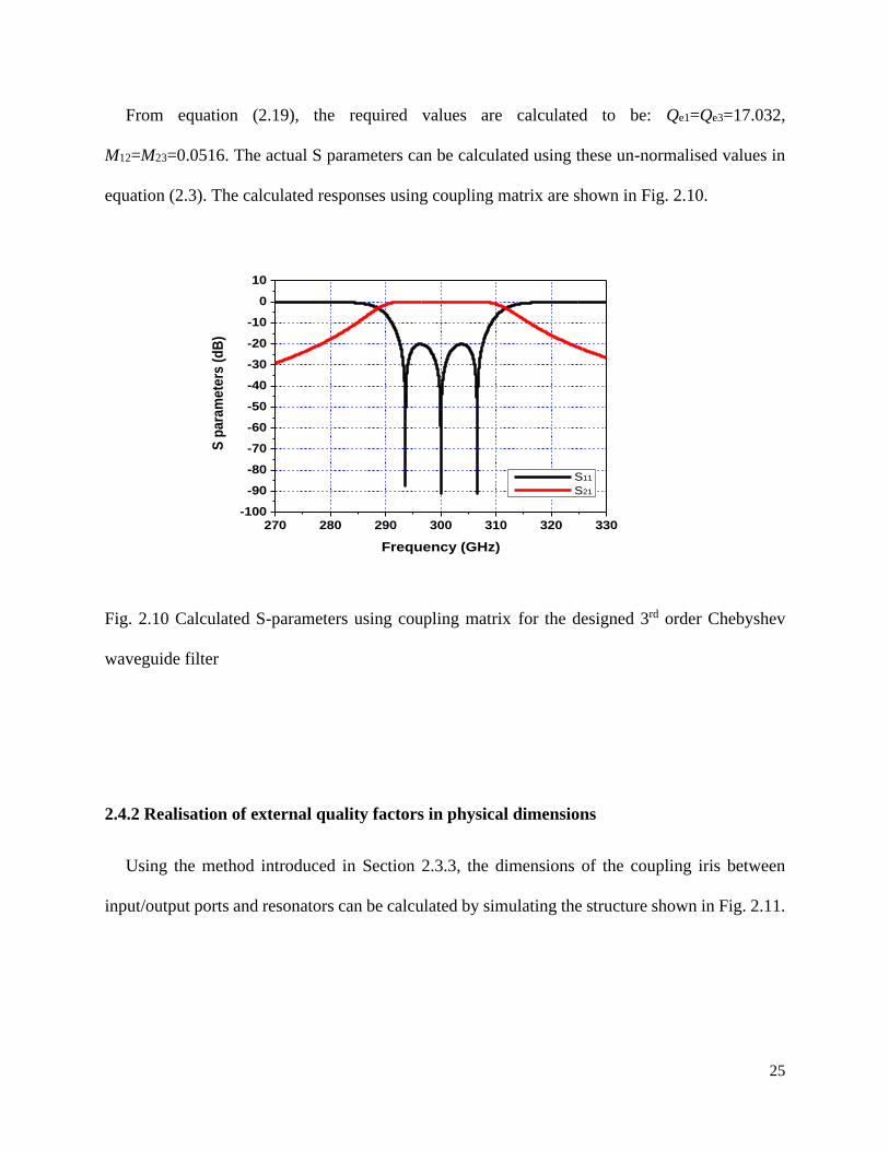
25
From equation (2.19), the required values are calculated to be: Qe1=Qe3=17.032,
M12=M23=0.0516. The actual S parameters can be calculated using these un-normalised values in
equation (2.3). The calculated responses using coupling matrix are shown in Fig. 2.10.
270 280 290 300 310 320 330-100
-90
-80
-70
-60
-50
-40
-30
-20
-10
0
10
S p
ara
me
ters
(d
B)
Frequency (GHz)
S11
S21
Fig. 2.10 Calculated S-parameters using coupling matrix for the designed 3rd order Chebyshev
waveguide filter
2.4.2 Realisation of external quality factors in physical dimensions
Using the method introduced in Section 2.3.3, the dimensions of the coupling iris between
input/output ports and resonators can be calculated by simulating the structure shown in Fig. 2.11.
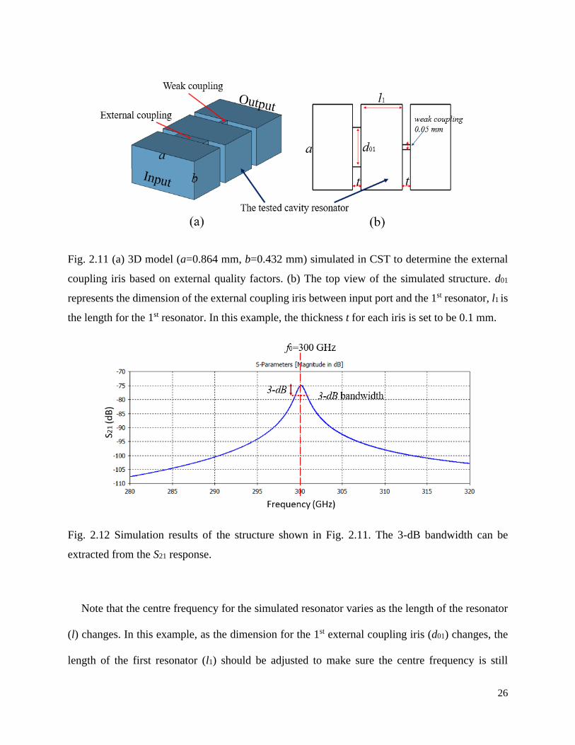
26
Fig. 2.11 (a) 3D model (a=0.864 mm, b=0.432 mm) simulated in CST to determine the external
coupling iris based on external quality factors. (b) The top view of the simulated structure. d01
represents the dimension of the external coupling iris between input port and the 1st resonator, l1 is
the length for the 1st resonator. In this example, the thickness t for each iris is set to be 0.1 mm.
Fig. 2.12 Simulation results of the structure shown in Fig. 2.11. The 3-dB bandwidth can be
extracted from the S21 response.
Note that the centre frequency for the simulated resonator varies as the length of the resonator
(l) changes. In this example, as the dimension for the 1st external coupling iris (d01) changes, the
length of the first resonator (l1) should be adjusted to make sure the centre frequency is still

27
300 GHz. By repeating these steps for different dimensions of external coupling iris and then
substituting the centre frequency (300 GHz) and the 3-dB bandwidth obtained from the simulations
into equation (2.15), we can get a series of l1 and d01 with corresponded Qe values, as shown in
Table-2.1.
Table-2.1 Simulated results to extract external quality factor from physical dimensions
f0=300 GHz
d01 (mm) 0.30 0.35 0.40 0.45 0.50
l1 (mm) 0.572 0.559 0.530 0.507 0.480
Qe1 245.6 84.1 31.8 15.2 7.1
Seen from Table-2.1, we can figure out that the suitable values for d01 is between 0.40-0.45 mm,
and the suitable values for l1 is between 0.507-0.530 mm. Through more detailed simulations
(using parameter sweeps in CST), d01=0.438 mm and l1=0.511 mm are selected as the initial
dimensions to achieve the calculated external factor (Qe1=17.032) for this example.
2.4.3 Realisation of coupling coefficients in physical dimensions
As introduced in Section 2.3.3, the dimensions of the coupling iris between resonators can be
determined by simulating the structure shown in Fig. 2.13. The simulated results for the structure
are given in Fig. 2.14.

28
Fig. 2.13 (a) 3D model (a=0.864 mm, b=0.432 mm) simulated in CST to determine the dimensions
of coupling iris between resonators. (b) The top view of the simulated structure. d12 represents the
width of the coupling iris between resonators, l2 is the length for the 2nd resonator. In this simulation,
the thickness t for each iris is also set to be 0.1 mm.
Fig. 2.14 The simulated S21 response for the of two coupled resonators shown in Fig. 2.13. f1 and
f2 are the two resonate frequencies for the structure.

29
Equation (2.18) gives the relationship between coupling coefficient and two resonate frequency
(f1 and f2). From the simulations, the coupling coefficients can be controlled by adjusting the width
of the coupling iris (d12). Note that the length for the resonator (l2) should also be adjusted to ensure
the middle frequency of two resonate peaks (f1 + f2)/2 is at centre frequency f0 of 300 GHz for this
example. Using equation (2.18), applying the actual frequencies of two resonate peaks, we can get
the actual coupling coefficient M12 between resonator 1 and resonator 2. The results for the
simulations are given in Table-2.2.
Table 2.2 Simulated results to extract coupling coefficients form physical dimensions
(f1 + f2)/2=f0 (300 GHz)
d12 (mm) 0.310 0.320 0.330 0.340 0.350
l2 (mm) 0.564 0.562 0.560 0.558 0.556
M12 0.0456 0.0498 0.0555 0.0605 0.0663
From Table 2.2, we can figure out that the suitable values for d12 is between 0.320-0.330 mm,
and the suitable values for l2 is between 0.560-0.562 mm. After more detailed simulations, to
obtain the required coupling coefficients (M12=M23=0.0516), d12=0.322 mm and l2=0.561 mm are
selected as the initial values for the width of the coupling iris.
2.4.4 Final optimisation
After extracting the initial values for the dimensions of the filter structures from coupling matrix
elements, three resonators are connected in series and externally coupled with input/output port to
establish the 3rd order Chebyshev bandpass filter. The simulation results using the initial values

30
for the dimensions are shown in Fig. 2.15. Seen from the initial simulated results, the responses
can roughly meet the requirements except for the shift in passband frequencies. Then further CST
optimisations have been applied to achieve the specifications by adjusting dimensions such as
length of the resonators and width of coupling iris. The final responses after optimisations are
presented in Fig. 2.15 and the optimised dimensions are given in Fig. 2.16.
Fig. 2.15 CST simulated S-parameters responses using initial values (dash lines) and responses
after optimisations (solid lines).
Fig. 2.16 The top view of the 3rd order Chebyshev filter with optimised dimensions. The optimised
dimensions for the filter structures are: l1=l3=0.460 mm, l2=0.517 mm, d01=d40=0.442 mm,
d12=d23=0.318mm, t=0.1 mm,

31
2.5 Conclusions
The background theories for the filter based on coupled resonators have been presented in this
chapter. It starts with the introduction of coupling matrix representation for the resonator-based
filters. This is followed by the discussion of characteristic for the rectangular waveguides, cavity
resonators and coupling iris. Then the methods of realisation of physical dimensions based on
coupling matrix are explained in detail. Finally, the design process of a 3rd order Chebyshev
waveguide filter is given as an example. Note that it is very important to obtain a relatively accurate
initial values since the optimisation process may fail to achieve the specification if the initial values
are too far from the solution results.
Reference:
[1] D. M. Pozar, Microwave Engineering. Third edition, John Wiley & Sons, Inc, 2005
[2] J. Hong and M. J. Lancaster, Microstrip Filters for RF/Microwave Applications. New York,
USA: Wiley, 2001.
[3] R. J. Cameron, C. M. Kudsia, R.R. Mansour, Microwave Filters for Communication Systems:
Fundamentals, Design and Applications. Hoboken, NJ, USA: Wiley, 2007.
[4] N. J. Cronin, Microwave and Optical Waveguides. IOP Publishing Ltd, 1995.
[5] J. Hong, “Couplings of asynchronously tuned coupled microwave resonators,” IET Microw.,
Antennas Propag., vol.147, no.5, pp.354-358, Oct. 2000.

32
Chapter 3
Micromachining for Terahertz Waveguide Circuits
As introduced in Chapter 1, the waveguide, usually in the form of a rectangular metal or
metallised tube, is an ideal low loss medium for the connection and construction of passive circuits
compared with other types of transmission lines operating at the same frequencies [1]. Due to its
low loss characteristics, the waveguide becomes more and more popular, especially for circuits
operating at frequencies at about 0.1 THz and beyond. However, as frequency goes up, the size of
the waveguide decreases and the tolerance on dimensions become more stringent, which bring
huge challenges and high cost to the conventional fabrication techniques such as CNC (Computer
Numerical Controlled) machining. From the review of Chapter 2, for waveguide filters based on
coupled cavity resonators, the dimensional accuracy is the primal challenge since their resonant
frequencies depend on the accuracy of dimensions of the length of resonator cavities (primarily
the length but other dimensions also) and external quality factor and coupling coefficients are
sensitive to the dimensions of the coupling iris. Researchers have been actively studying this and
different manufacturing techniques have been proposed and developed for the fabrication of
complex terahertz circuits with improved dimensional accuracy and reduced cost [2]. The current
states of these micromachining techniques will be reviewed and presented in Section 3.1.
The SU-8 photoresist technology and laser micromachining are the two emerging
micromachining techniques which are employed in this work to fabricate the waveguide devices
working at WR-3 band (220-325 GHz). The detailed process of SU-8 photoresist technique [3] is
presented in Section 3.2 and a novel multi-stage process for laser micromachining is discussed in
Section 5.2.2, while the micromachined terahertz circuits using those two techniques are described

33
in Chapter 4 and Chapter 5.
3.1 Overview of Micromachining Techniques for Terahertz Waveguide Circuits
Fabricating terahertz circuits using traditional process, such as CNC milling, can be extremely
expensive and hard to achieve demanding dimensional accuracy at high frequency. Different
micromachining techniques such as silicon deep reactive ion etching (DRIE) [4-5], lithographic
micromachining technique (LIGA) [6] and SU-8 photoresist technology [7-8], have been
developed and utilised in fabricating terahertz waveguide filters with high-dimensional accuracy.
Laser micromachining [9] and 3-D printing [10] have also been utilised for high frequency filters
by the authors using different designs at about 0.1 THz [3]. The general introduction for these
different fabrication techniques is presented in the following subsections.
3.1.1 CNC milling
Traditionally, for geometrically simple metal waveguide circuits operating at lower frequency,
the main fabricating process is by milling on a high precision CNC machine, usually using a split-
block technique [2]. Recently, for waveguide components operating around 100 GHz, the CNC
milled waveguide filters with excellent performance have been reported. Two 4th order Chebyshev
waveguide filters operating on W-band are presented in references [11] and [12]. The first filter is
centred at 92.6 GHz and measured to have 0.5 dB insertion loss with fractional bandwidth (FBW)
of 4.53%. In [12], the filter is centred at 100 GHz with 10 GHz bandwidth and measured to have
0.6 dB insertion loss within passband. For the 220 to 325 GHz WR-3 band, waveguide features

34
and tolerances decrease by a factor of around three. Fabricating waveguide filters at such a
frequency requires an expensive, high precision CNC mill [3]. Filter design flexibility is also
limited by tool sizes and depth to diameter aspect ratios [12]. However, researchers are still
pushing the limits of conventional CNC milling: two fourth order CNC milled waveguide filters
working on WR-3 band are presented in [13], one with measured 0.7 dB insertion loss and 8.77%
(22.6 GHz) bandwidth and another with measured 0.5 dB insertion loss and 9.83% (25.2 GHz)
bandwidth. High frequency CNC machined waveguide circuits are reported by Jet Propulsion
Laboratory (JPL). The CNC milling process is successfully developed and employed to fabricate
several waveguide circuits operating at terahertz frequencies (up to 1.5 THz), with a high
dimensional accuracy [14] (typically within 2 µm deviation from designed value). Figure 3.1
shows the two terahertz waveguide circuits reported in [14], fabricated by the JPL using high
precision end-mil machining technique. For fabricating complex terahertz waveguide circuits,
further improvements are being made with CNC milling process. An example of a purpose-built
ultra-high precision CNC micromachining platform as shown in Fig. 3.2 is developed and reported
in [15]. This represents the current state-of-the-art CNC machining technique, with typical
measured dimensional accuracies of 2-3 µm, surface roughness of 75 nm and tools of sizes
available between 25 µm and 10 mm (with aspect ratio greater than 5:1). Several waveguide
circuits including highly integrated blocks operating at frequencies ranging from W-band to 2.7
THz were successfully produced via this platform [15].
Although these good examples show that CNC milling method is still capable for the terahertz
waveguide circuits fabrication, the drawbacks of this technique is obvious: (i) As frequency
increases, the feature size decreases, and the unit cost will increase dramatically due to the
requirement of feasible high precision CNC mill. (ii) To fulfil the strength requirements of the

35
milling cutter, the depth to diameter ratio usually needs to be less than about 3:1, which means
some narrow trenches or iris are not possible for CNC milling process to fabricate. (iii) Round
internal corners are almost inevitable due to the chosen milling cutter in the fabrication process.
(iv) It is not a good choice for large scale production since it is a serial processing method [14] (v)
expensive, specialist CNC machine tools are required.
In this work, a CNC milled extracted pole filter operating at WR-3 band (220-325 GHz) with
an improved performance is presented in Chapter 4.
Figure 3.1 State-of-art terahertz waveguide circuits using CNC milling by JPL (a) A quad-chip
tripler operating at 260-360 GHz (b) A balanced HEB mixer with integrated feed horns working
at 1.5 THz. (Figure reproduced from [14])

36
Fig. 3.2 The Kern Model 44 (left) and Kern MMP (right) high precision CNC milling platform
used at Arizona State University and the University of Arizona [15].
3.1.2 Si deep reactive ion etching (DRIE)
DRIE is a popular micromachining technique. This process can be basically categorized into
bulk micromachining.
Bulk micromachining is a method that fabricates structures by selectively etching material from
a bulk substrate [16]. Although various different materials can be used as the substrate for bulk
micromachining, silicon is being used for that purpose in most cases because of the greater level
of experience with this material, achieved through the production of semiconductor devices [15].
Ceramic, plastic or glass materials could be the potential alternate materials to Si [17]. However,
according to the state-of-art techniques, silicon provides the best characteristics in terms of cost,

37
machinability and metallisation.
DRIE of bulk silicon wafers is a fabrication technique that can produce deep structures,
typically with high aspect ratios, in a silicon substrate [18]. This is an attractive technique for the
fabrication of terahertz waveguide circuits. Examples of waveguide filters using DRIE process
working on W-2.2 band, W-1.5 band and W-1 band can be found in literature [19-21]. This
lithography-based process is ideally suited for large size batch production, and is capable of
offering uniformity between batches [2]. Fig. 3.3 presents the six key steps for the DRIE process
and these steps can be summarised as:
(i) Silicon oxide (i.e. SiO2) is deposited on both side of the substrate wafer as a SiO2 mask layer
and a SiO2 stop layer;
(ii) Apply photoresist on top of the SiO2 mask layer;
(iii) After patterning and developing the photoresist layer, the exposed SiO2 mask layer is
etched to form the oxide mask;
(iv) Remove the photoresist layer then etch the silicon substrate to form the desired structures;
(v) Remove the SiO2 mask layer and SiO2 stop layer by using buffered oxide etch (BOE)
solution;
(vi) Metallise the fabricated silicon layer with Ti layer and Cu layer.

38
Fig. 3.3 Key steps for DRIE process [22]
Compared with CNC machining, DRIE can be utilised in high frequencies applications and has
drawn more attention due to its shorter fabrication time, higher aspect ratios (>30:1) and excellent
critical dimension control [22]. However, DRIE process for micromachining suffers from four
main problems: (i) hard to achieve vertical (~90°) sidewalls; (ii) difficult to obtain uniform depth
across the wafer for each etch depth [23]; (iii) relatively poor surface roughness on the sidewalls
[24]; (iv) the height of structure is limited by commercially available silicon wafer thickness [25].
More efforts have been put onto DRIE process in order to address these problems to a
certain extent [24]. Typically, the dimension deviations within 2 µm and less than 3° sidewall draft
angles have been achieved for a well-established DRIE process [26]. Note that these tolerances
vary with wafer thickness. As for draft angles on side walls, reference [22] reports improved

39
etching angles as low as 0.5°, measured on a WR-1 waveguide filter. This filter also has the best
reported surface roughness of 100 nm [22]. Normally, for waveguide circuits built using DRIE
process, they are formed by two etched silicon pieces and within each piece only features of the
same depth are allowed. Recently, a further advancement on the technique is reported in [26], in
which presents a multistep DRIE process that can fabricate different depths for arbitrary
waveguide features within same silicon piece with ±2% tolerance. This additional flexibility
allows more complex waveguide devices to be constructed and enables the possibility of
integration of multiple components onto a single silicon package.
3.1.3 LIGA process [28]
LIGA is an acronym of German terms Lithographie, Galvanoformung and Abformung, which
correspond to the three English words as Lithography, Electroforming and Moulding that describe
the three key steps for this fabrication technique. Fig. 3.4 presents the standard steps that have been
utilised in LIGA process. The first thing for the LIGA process is coating the substrate (normally a
silicon wafer) with X-ray sensitive resist. Typically, Poly (methyl methacrylate) (PMMA) is
chosen as the resist and applied to the substrate by a glue-down process [27]. Then the resist is
patterned by exposure to the X-ray through an X-ray mask with high resolution features. During
the development process, for structures with high aspect-ratios, the ratio of dissolution rates for
the resist-developer system in the exposed and unexposed areas should be 1000:1. The empirically
optimised developer which provides the required ratio of dissolution rates can reduce stress-related
cracking from swelling compared with conventional PMMA developers [28]. In the next step, the
substrate is rinsed with deionized water and the resist (PMMA) microstructures can be released as

40
the final product (e.g., optical components) or can be used as an electroplating template to produce
the metal master mould. This metal mould is with high dimensional accuracy and can be utilised
for mass production of desired plastic microstructures with injection moulding, as shown in
Fig. 3.4.
The light source of LIGA, the synchrotron generated X-rays, have a deeply penetrating
capability. With high energy X-rays, it is able to pattern resist (e.g. PMMA) with thicknesses of
millimetre scale and achieve better than 100:1 aspect ratio [27]. In addition, in the lithography
process, the using of X-ray gives the advantage that diffraction effects can be reduced due to its
short wavelength [27], thus provide high accuracy of sub-micrometre dimensional control.
Moreover, X-rays are able penetrate thick resists with less than 0.1 µm horizontal run-out per 100
µm thickness. This provides extremely vertical sidewalls with very small surface roughness (rms
(root mean squared) roughness is better than 20 nm) [28].
Compared with typical DRIE process, the LIGA process is able to fabricate nearly perfect
geometries in terms of aspect ratio, vertical sidewalls, pattern precisions and achievable thickness.
However, the biggest drawback for this micromachining technique is that the cost is very high (e.g.
X-ray sources and X-ray masks) for research purpose or small-scale production. For mass
production purposes, it is believed that LIGA process is a good choice for fabricating
microstructure [10].

41
Fig. 3.4 Key steps for the LIGA process [28]
3.1.4 SU-8 photoresist technology for micromachining
SU-8 micromachining is a photolithographically-based process, which is another promising
technology for manufacturing millimetre-wave and terahertz waveguide components [3]. SU-8 is
capable of constructing three-dimensional (3D) terahertz waveguide structures with high aspect
ratios (greater than 50:1), high dimensional accuracy (tolerance within 2 µm), and excellent surface
roughness (better than 50 nm of rms roughness) [30].
Compared with CNC machining, SU-8 micromachining has several advantages. For example,
SU-8 can achieve a similar high dimensional accuracy with potentially lower cost. It may also
allow sharper internal corners and higher corner radius to depth ratios [3]. Meanwhile, SU-8

42
process is a batch fabrication which allows repeatability between devices as well as production of
several devices in a single fabrication run [31]. Compared with DRIE, standard photolithography
processes are used with SU-8 with better surface roughness on the sidewalls of waveguide
structures [31].
The SU-8 process has been widely employed in terahertz circuits, such as W-band filters in [7],
WR-3 band waveguide filters in [8], and WR-1.5 in [32].
At the EDT group of the University of Birmingham, the SU-8 process has been developed over
the past decade, and successfully applied to a series of passive circuits [7-8, 30, 32]. In Section 3.2,
the detailed process of SU-8 micromachining is described and in Chapter 4, a novel WR-3 band
waveguide filter, designed to meet a required specification, fabricated using the SU-8
photolithography process, will be given as an example.
3.1.5 Laser micromachining
Laser micromachining is another attractive alternative for the fabrication of microstructures and
has the potential of manufacturing terahertz waveguide components [2]. The laser light, which has
high power density and low angle divergence, can also be employed in micromachining. The laser
micromachining is a fabrication technique that directs the output of a high-power laser through an
optic system and then uses the laser beam to remove materials [33]. By directing the focused beam
at the material, it is able to melt, burn or vaporize away a part of the material, producing
microstructures with high-quality surfaces [33].
Three main types of lasers are utilised in laser micromachining: carbon dioxide (CO2) lasers,

43
the neodymium YAG (Nd-YAG) lasers and excimer lasers. The carbon dioxide lasers are typically
employed in industry cutting of many materials such as metal, plastic and fabrics. The Nd-YAG
lasers are used where very high power is needed and are commonly used for cutting and scribing
metals and ceramics [33]. Both CO2 and Nd-YAG lasers are infrared (IR) lasers, which make use
of localized heating by a laser beam spot. IR lasers are suited for three main micromachining
applications: drilling and cutting, welding, or heat treatment [34]. The biggest drawback of IR
lasers is that, with high power beam directing at the cutting area, the material adjacent to the
fabricated surfaces will be affected by the relatively high temperature [33].
An excimer laser is a form of ultraviolet (UV) laser and are commonly used for the fabrication
of industrial microstructures with 0.05–1000 µm feature sizes [34]. This kind of laser affects the
chemical bond within the material and transfer the material from solid to gas. In order to selectively
remove the material and pattern the structures, a mask similar to that utilised in photolithography-
based process is applied [34]. Different from typical silicon-etching-based process or
photolithography-based process, the cutting depth can be controlled by adjusting the number of
pulses. Depth of several hundred microns and vertical or tapered (by tuning the angle of the
incident laser beam) sidewalls can be achieved. The excimer laser is usually utilised in the cutting
for polymer or silicon materials, or sometimes can be employed in fabricating thin metal layers if
the system supports sufficient laser power densities.
Laser micromachining has some very appealing advantages compared with existing processes.
Compared to CNC machining, laser micromachining is able to achieve high dimensional and
geometrical accuracy for tiny features (as small as 10-20 µm). Since laser micromachining is a
non-contact process, which gets rid of the generation of defects and cracks due to mechanical
stresses [2]. Compared with DRIE process, LIGA-based electroplating process and SU-8

44
photoresist techniques, laser micromachining is another great choice since it is capable of
producing complex features with multiple depths and it offers relatively high accuracy (<10 um)
and repeatability. It can be applied to different materials (including metal) as well. Laser
micromachining is reported to be employed for the fabrication of various optical or quasi-optical
components, such as terahertz metal mesh filters [35]. However, from the literature, laser cutting
is rarely utilised to produce terahertz waveguide components, except for a W-band waveguide
filter presented in [9] and a 2-THz horn antenna laser cut from silicon [35].
In general, the main advantages that laser micromachining provides over other micromachining
techniques are: (i) It can be applied to different materials including metal. Almost all metal devices
are allowed to be fabricated, and this offers an attractive choice to scenarios where a higher thermal
stability of the devices is required [2]. (ii) It is capable of producing complex 3-D waveguide
structures with varying depths (or heights) from one workpiece and thus eliminates the need for
splitting the device into several layers and then assembling them with a high accuracy [7]. (iii)
Laser cutting system are highly flexible and can be configured to cut, drill, weld, engrave and
deposit materials, which is cost effectively and allowing modification in the design. Therefore,
laser micromachining is an excellent choice for the small to medium batch size production of
terahertz waveguide devices.
In Chapter 5, a novel hybrid manufacturing approach combining CNC milling with laser
micromachining is introduced. Two WR-3 band waveguide filters, which are specifically designed
to take advantage of the laser micromachining fabrication process, are presented in Chapter 5.

45
3.1.6 3-D printing
3-D printing, or additive manufacturing, is another promising technique to produce low
terahertz frequency waveguide circuits. One of the potential advantages of using 3-D printing for
millimetre-wave and terahertz applications is the potential weight reduction by replacing the
conventional metals with metallised polymer materials. The filter can also be specially designed
and appropriately fabricated to reduce its mass by removing material at current nulls in the
resonator structure [38]. Another advantage is that 3-D printing enables complex geometry designs
compared to CNC milling or silicon etching process. For example, filters based on spherical
resonators working on X-band shown in [38] which have ultra-high unloaded quality factors can
be easily made using 3-D printing and this design can be scaled to operate in low terahertz
frequencies. There are basically three additive manufacturing techniques, stereolithography
apparatus (SLA), selective laser sintering (SLS) and fused deposited modelling (FDM), which are
most commonly used for micromachining. From the latest literature, SLA process offers the
highest resolution and the best surface integrity [38]. For the state-of-the-art SLA process
presented in [39], the tolerance of dimensional accuracy is within 25 µm and the surface roughness
is better than 1 µm. Good results of waveguide filters fabricated using SLA can be found in [39],
with the highest reported frequencies operating at W-band [39]. SLS process is suited for the
fabrication of all-metal waveguide structures, at the penalty of relatively lower dimensional
accuracy and worse surface roughness [2]. Two examples of waveguide filters using SLS process
(printed using copper) operating at E-band (60-90 GHz) can be found in [40] with relatively poor
performance. According to the research in [40], there are mainly two reasons that attribute to the
deviation between simulated and measured response. The first is that the surface roughness of the
filter is measured to be 6 µm which can have significant influence to the response. The other reason

46
is that the fabricated dimensions shrink by around 2-3% compared to the designed values [40].
Further research has been done in [41]. Two fifth order filters operating at W-band, one made from
stainless steel and the other made from stainless steel coated with copper, are fabricated and tested.
The insertion loss within passband are measured to be 1.9 dB and 1.0 dB for the stainless-steel
filter and copper coted filter respectively. The filters presented in [41] are currently the highest
frequency waveguide filters fabricated using SLS process with the best performance.
Note that the 3-D printing technique is new and not able to achieve terahertz specifications at
the moment. However, the development of this novel micromachining process is fast and the
dimensional accuracy for this technique is expected to improve significantly over time. This is a
promising technique with the potential for terahertz circuit to be fabricated using 3-D printing
technique soon.
3.2 Fabrication Process for SU-8 Photoresist Technology
SU-8 photoresist technology for micromachining have been employed for fabricating a range
of waveguide circuits. The SU-8 resist is sensitive to ultraviolet (UV) light, which means that
employing the relatively cheaper UV-lithography process is possible. Since SU-8 is a
photosensitive material, standard photolithography process can be utilised to define prescribed
micro-patterns accurately by selective exposure to UV radiation through a mask [42]. These
outstanding characteristics of SU-8 make it an attractive choice as the material for micromachining.
There are two different process to fabricating waveguide filters. One is SU-8 single layer
lithography which mainly employed for fabricating microstructures with relatively simple

47
geometries. The other is SU-8 two-layer lithography processes which is developed for more
complex waveguide devices [2]. The key steps of the typical SU-8 process include [43]: (i) spin
coating, (ii) soft bake, (iii) exposure, (iv) post-exposure baking, (v) development, (vi) hard baking,
(vii) substrate removal, and (viii) metallization. Figure 3.5 illustrates these basic steps for SU-8
single-layer and two-layer processing. The general fabrication process utilised in the waveguide
circuit presented in this thesis is described with a schematic in the following part.
(h) Development of the SU-8
two- layer structure
(a) Spin coat SU-8 layer
onto silicon substrate(c) First SU-8 layer is
exposed using UV light
Chrome
mask1
Chrome
mask 2
(e) Post exposure bake the
first SU-8 layer to form weak
crosslink
(g) Exposure of the second SU-8 layer and
postexposure bake to form strong crosslink
(d) Post exposure bake and
development (followed by
hard bake and substrate
removal)
(f) Spin coat the 2nd
SU-8 layer
Silicon wafer
SU-8 photoresist
Cross-linked SU-8
UV light
Two-layer process
(b) Pre-exposure bake
Baking using
hot plate
Fig. 3.5 Basic steps for SU-8 single-layer and two-layer processes. (Figure reproduced from [2])
3.2.1 Spin coating
The SU-8 photoresist is commonly stored as liquid form. In the first step, the liquid SU-8 is
well spread on a flat silicon substrate with a desired thickness via spin coating process [43]. As

48
shown in Figure 3.4 (a), a measured amount of the SU-8 photoresist is added to the top of a cleaned
silicon wafer (using H2SO4 and H2O2, then rinsing with de-ionized water and drying in air) which
is fixed on a spinner. After the wafer spun around with appropriate speed, the SU-8 photoresist
will be distributed uniformly over the surface of silicon wafer due to the effect of centrifugal forces.
The spin speed is typically depended on the resist type and required resist thickness [15]. Normally
to fabricate devices with thinner layer thickness required higher spin speed. For the SU-8
micromachined waveguide filter operating on WR-3 band presented in this work, the designed
layer thickness is 432 µm. Precision weight control for the SU-8 photoresist has been employed in
order to accurately control the layer thickness.
3.2.2 Soft bake
The soft bake process, or can be called as pre-exposure bake, is aimed at drying out the solvents
from the SU-8 resist. This process is typically carried on with an infrared oven, a microwave oven
or a level hot plate [43]. Among these choices, the level hot plate offers the best thermal control.
In this work, as shown in Figure 3.4 (b), the soft bake is performed on a hot plate, which is precision
levelled to ensure the uniform thickness for each SU-8 layer [43]. The resist is first baked at 65°
C for 20 minutes, and then baked at 95° C for usually 4-6 hours (depending on the required
thickness). The first 65°C baking step is to assist self-planarization of the SU-8 photoresist and
produces better thickness uniformity for each fabricated SU-8 layer [42], while the main purpose
of the second step of soft baking at 95°C is driving off the solvent.

49
3.2.3 Exposure
As shown in Figure 3.4 (c), after pre-bake, the SU-8 photoresist is exposed under UV light
through a designed mask to define patterns of the waveguide structures. The mask is usually made
by a piece of transparent glass covered by patterned chromium [43]. The parts on the glass that
covered by chromium correspond to the filter features that are selectively removed. By projecting
UV light onto the mask, the pattern is transformed from mask to the photoresist, since glass is
transparent to UV light, whereas the parts covered by chromium are non-transparent.
Usually an UV lamp with proper incident energy (J/cm2) is used to produce the incident light
on the photoresist through the mask. The choice of incident energy is mainly decided by the required
photoresist thickness. According to the reaction when exposed to light, the photoresists can be
basically grouped into two categories: positive resists and negative resists. For positive/negative
resists, the chemical bonds are weakened/strengthened while exposing to light and the exposed
parts become more soluble/insoluble [16]. In this case, positive resists will obtain same patterns
with the mask after the development process, while negative resists will gain opposite patterns
with the mask. For this work, SU-8 is a typical negative photoresist. After exposure under UV
light, the SU-8 resist will produce a photoacid which can perform as a catalyst in the cross-linking
reactions during the post exposure bake process [15].
3.2.4 Post exposure bake
Since SU-8 is a negative resist, the post exposure bake is a necessary step for producing the
cross-linking reactions [33]. Figure 3.4 (d) and (e) present the post exposure bake process for

50
single-layer and two-layer SU-8 process. By post exposure bake at 60-100°C, the rates of cross-
linking reactions increase and the exposed areas will become insoluble in the developer. To ensure
the quality of the final products and avoid the cracking of the SU-8 samples, the bake time should
be precisely controlled. Longer post-bake time can increase the stress within the resist and cause
bending of the final structures while shorter bake time may result in some exposed areas not fully
cross-linked (i.e. soluble to solvents in the development step). Generally, the post exposure bake
process is firstly carried out on a conventional oven or a hot plate at 65° C for 2 minutes, and then
ramped up to 95° C for 30 minutes. After switching off the heater, the wafer is left on the oven or
the hot plate to gradually cool down to room temperature [42].
3.2.5 Development
The development process, as shown in Figure 3.4 (d) for single layer-process and (h) for two-
layer process, is usually employed after post exposure bake to remove the unwanted SU-8 resist
(non-cross-linked area). This process is performed by immersing the exposed and baked resist
together with the silicon wafer into the developer solution at room temperature for about 30 mins.
The immersing time can be different according to the designed thickness and required aspect ratio
of the SU-8 layer [44]. In order to increase the development rate, a strong agitation, which can
enhance diffusion of developer molecules with the non-cross-linked SU-8 resist, is usually
required during the process [44]. Then the developed sample is rinsed using Isopropyl Alcohol
(IPA) and drying with a nitrogen gun. After completing this step, filter structures are formed
corresponding to the negative image of the designed mask.

51
3.2.6 Hard bake and substrate removal
After the development process, a hard bake process is recommended to enhance the cross-
linking bonds, which makes sure that the final structures of SU-8 resist is strong and can endure
common acids and alkalis, and also resilient to following process such as metal evaporation which
puts the SU-8 layers into environment with higher than 100° C temperature. The hard bake is
usually carried out on a hot plate at 150° C for 30 minutes. Without hard bake process, the SU-8
structures are susceptible to bending during metallisation process [45].
Due to strong bond associated with the cross-linking, it is usually difficult to separate the
patterned SU-8 layer from the silicon substrate. There are two ways to remove the substrate. The
first one is to put a layer of soluble resist below the SU-8 during the spin coating process and then
the patterned SU-8 layer is released by dissolving the sacrificial layer in tetramethylammonium-
hydroxide-based solution at room temperature for about 5 hours [44]. The second method is by
immersing the SU-8 layer together with the substrate in a 10% sodium hydroxide solution (i.e.
NaOH) [42]. This method requires immersing with temperature of 60° C for more than 7 hours to
fully etch the silicon away.
3.2.7 Metallisation
Sputtering and evaporation are commonly utilised for the metallisation process with the SU-8
layers [16]. To enhance the chemical bond between the SU-8 layers with the typical coating metal
such as silver or goad, a thin adhesive layer (i.e. 5 nm of Chromium (Cr) or Titanium (Ti) layer) is
firstly sputtered onto the surface of the SU-8 layers. The samples are then put in an evaporation

52
metal coater, in which silver or gold is vaporised by heating and then transported in vacuum to
condense on the surface of the SU-8 layers to be coated [42]. During sputtering and evaporation
process, the SU-8 layer is fixed on a tuneable sample holder which can rotate continuously in
different angles to ensure good coverage of coating on all the surfaces of the SU-8 pieces, including
the sidewalls [42].
3.2.8 Fabrication process for SU-8 two-layer processing
The SU-8 two-layer process is an optimised method developed for complex structures based on
the general SU-8 single-layer process. The difference between two method happens after the resist
exposed to UV light (i.e. after step shown in Fig. 3.5 (c)). For the general single layer process, the
structure is baked after exposure to form cross-link, developed in solution and then hard baked,
finally released from silicon wafer, as shown in Fig. 3.5 (d). However, for the SU-8 two-layer
process, the post exposure bake process would be carried out under relatively low temperature for
the first SU-8 layer to form weak crosslink. Then the SU-8 resist for the second layer is spin coated
on top of the first SU-8 layer, as shown in step (e) and (f). As presented in Fig. 3.5 (g)-(h), same
process utilised in single-layer process such as an exposure of UV light, post-exposure bake and
development are repeated for the second layer. The final product is a fully cross-linked and joined
two layered SU-8 structure, without internal joints [2].
Compared with the single layer process, in which the isolated islands structures (i.e. features
that can’t stand along without support) are not permitted, the two-layer process address the
problem of this restriction and allows standalone regions on the top layer [2]. This enables the
realisation of some complex waveguide filter designs. One example can be found in [46], in which

53
a WR-3 band cross-coupled dual-band filter is fabricated and measured. In addition, the two-layer
process is an efficient solution since it can eliminate the inner joints between layers and avoid
localized air gaps [2]. This is a significant improvement for waveguide devices based on SU-8
photoresist technology since this would reduce the energy loss through the gaps.
3.3 Conclusions
This chapter has given an overview of micromachining techniques for terahertz waveguide
circuits as well as general process of some recently developed micromachining techniques such as
DRIE process, LIGA process, SU-8 photoresist technology, laser micromachining and 3-D
printing. Table-3.1 shows the comparison of the maximum aspect ratio, dimensional accuracy and
achievable surface roughness for different micromachining techniques. This table presents the
state-of-art reported in literature for different micromachining techniques. Regardless of the cost,
devices and technicians that are required to accomplish the waveguide circuits, this comparison
only takes the best performances achieved by the researchers into account. Another table that
summaries the recent published waveguide filters (including the filters described in this thesis)
operating in frequency from the WR-10 to WR-1.5 band will be given in Chapter 4.
As introduced in this chapter, DRIE is relatively a mature technique utilised in micromachining.
Many researchers have already looked into this process to dig its potential in the fabrication of
terahertz circuits. However, to achieve high dimensional accuracy and low draft angles on
sidewalls, an extremely well-established DRIE process are required [22][26], which means that
experienced technicians and expensive machines with high accuracy are indispensable for the
research. Seen from the comparison in Table-3.1, LIGA process is the technique with best

54
achievable performances. However, the great cost and limited resources for this technique (e.g. X-
ray sources and X-ray masks) makes LIGA process not a good choice for research purpose or
small-scale production. Compared from reported micromachined circuits, 3D printing didn’t
provide any obvious advantages in performances, but 3D printing is definitely a promising
micromachining technique applied in terahertz circuits once the fabrication process for this
technique have been fully developed. Researchers in EDT group in University of Birmingham
have already successfully designed, fabricated and measured several waveguide circuits operating
at around 100 GHz with reasonable performances.
The choice of the micromachining techniques utilised in this work is mainly based on three
factors: (i) the potential of the technique utilised in machining terahertz circuits; (ii) the resources
that are available during the research process; (iii) the cost for research purpose. Balancing
between these factors, SU-8 photoresist technology is a promising micromachining process and
our EDT group in University of Birmingham has sufficient technical devices and experience for
fabricating SU-8 waveguide circuits operating at 100-300 GHz. From Table-3.1, laser
micromachining is not an attractive micromachining process since it is not able to achieve
demanding specifications of terahertz circuits at the moment. However, with the advantages of
repeatable at the micro-scale relatively high accuracy and able to fabricate a wide range of
materials with complex features, laser micromachining is a novel and promising technique for
fabricating terahertz waveguide circuits. More importantly, the School of Mechanical Engineering
in University of Birmingham provides us with resources such as instruments with high accuracy
and experienced technicians to investigate the application of laser micromachining in terahertz
circuits. From above reasons, SU-8 photoresist technology and laser micromachining have been
chosen and applied in the fabrication of terahertz filters in this work.

55
As SU-8 photoresist process is employed to fabricate some of the micromachined waveguide
circuits presented in this thesis, the detailed steps of the SU-8 fabrication process are also presented
in this chapter. The examples of the fabricated filter using SU-8 photoresist technology will be
presented in the following Chapter. The novel multi-stage process for laser micromachining will
be introduced and explained together with the designing of laser micromachined filters in
Chapter 5.
Table-3.1 Comparison of best performance of different micromachining techniques
Techniques
Achievable
aspect ratio
Dimensional
accuracy (µm)
Surface roughness Reference
CNC machining >5:1 <2 75 nm [14]
DRIE process >30:1 <2 100 nm [22]
LIGA process >100:1 <1 10 nm [28]
SU-8 process >20:1 <2 40 nm [32]
Laser machining >3:1 <10 1.25 µm [9]
3D printing (SLA) >100:1 <25 1 µm [39]
3D printing (SLS) >15:1 <50 2 µm [41]

56
References:
[1] N. J. Cronin: “Microwave and Optical Waveguides,” (Iop Publishing Ltd, 1995)
[2] X. Shang, H. Yang, D. Glynn, M. J. Lancaster. “Submillimeter-wave waveguide
filters fabricated by SU-8 process and laser micromachining” IET Microw., Antennas
Propag., vol. 11, no. 14, pp. 2027-2034, Nov. 2017.
[3] H. Yang, Y. Dhayalan, X. Shang, M. J. Lancaster, et al., “WR-3 waveguide filter
based on high precision CNC milling and SU-8 photoresist technology,” IEEE Trans.
THz Sci. Technol., vol. 8, no. 1, pp. 100-107, Jan. 2018.
[4] J. Y. Li, B. Pan, C. Lugo, M. Tentzeris, and J. Papapolymerou, “Design and
characterization of aW-band micromachined cavity filter including a novel integrated
transition from CPW feeding lines,” IEEE Trans. Microw. Theory Tech., vol. 55, no.
12, pp. 2902–2910, Dec. 2007.
[5] K. M., K. H. Leong et al., “WR1.5 Silicon Micromachined Waveguide
Components and Active Circuit Integration Methodology,” IEEE Trans. Microw.
Theory Tech., vol. 60, no. 4, pp. 998-1005, Apr. 2012.
[6] J. R. Stanec and N. S. Barker, “Fabrication and integration of micromachined
submillimeter-wave circuits,” IEEE Microw. Wireless Compon. Lett., vol. 21, no. 8, pp.
409–411, Aug. 2011.
[7] X. Shang, M. Ke, Y. Wang and M. J. Lancaster, “Micromachined W-band
waveguide and filter with two embedded H-plane bends,” IET Microw., Antennas
Propag., vol. 5, no. 3, pp. 334-339, Feb. 2011.
[8] Q. Chen, X. Shang, Y. Tian, J. Xu and M. J. Lancaster, “SU-8 micromachined

57
WR-3 band waveguide bandpass filter with low insertion loss,” Electron Lett., vol. 49,
no. 7, pp. 480-482, March. 2013.
[9] X. Shang et al., "W-Band Waveguide Filters Fabricated by Laser Micromachining
and 3-D Printing," IEEE Trans. Microw. Theory Tech., vol. 64, no. 8, pp. 2572-2580,
Aug. 2016.
[10] C. Guo, J. Li, D. D. Dinh, X. Shang, M. J. Lancaster and J. Xu, "Ceramic filled
resin-based 3D printed X-band dual-mode bandpass filter with enhanced thermal
handling capability," Electronics Letters, vol. 52, no. 23, pp. 1929-1931, 11 10 2016.
[11] X. Liao, L. Wan, Y. Yin and Y. Zhang, “W-band low-loss bandpass filter using
rectangular resonant cavities,” IET Microw., Antennas Propag., vol. 8, no. 15, pp. 1440-
1444, Sep. 2014.
[12] C. A. Leal-Sevillano, J. R. Montejo-Garai, J. A. Ruiz-Cruz and J. M. Rebollar,
"Low-Loss Elliptical Response Filter at 100 GHz," IEEE Microw. Wireless Compon.
Lett., vol. 22, no. 9, pp. 459-461, Sep. 2012.
[13] J. Q. Ding, S. C. Shi, K. Zhou, Y. Zhao, D. Liu and W. Wu, “WR-3 Band Quasi-
Elliptical Waveguide Filters Using Higher Order Mode Resonances,” IEEE Trans. THz
Sci. Technol., vol. 7, no. 3, pp. 302-309, May. 2017.
[14] P. J. Bruneau, H. D. Janzen, J. S. Ward, “Machining of Terahertz Split-Block
Waveguides with Micrometer Precision,” 33rd International conference on IRMMW-
Terahertz, 2008.
[15] C. E. Groppi, B. Love, M. Underhill, et al.: “Automated CNC micromachining for
integrated THz waveguide circuits,” Proc. 21th Int. Symp. Space THz Technolo, Oxford,
23-25 March 2010

58
[16] H. T. Ran, “MEMS and Microsystems: Design, Manufacture, and Nanoscale
Engineering” (2nd edition, Wiley)
[17] Bulk micromachining from University of Maryland [online], available at
http://terpconnect.umd.edu/~sandborn/research/JPL_MEMS/microeng_bulk.html
[18] J. L. Yeh, A. H. Jiang, and N. C. Tien. “Integrated polysilicon and DRIE bulk
silicon micromachining for an electrostatic torsional actuator.” Journal of
Microelectromechanical Systems, 1999, pp.456-465.
[19] S. Biber, J. Schur, L.P. Schmidt, “Technological Issues for Micromachining of New
Passive THz Components Based on Deep Trench Silicon Etching,” Infrared and
Millimeter Waves, 12th International Conference on Terahertz Electronics, 2004, pp.
145 – 146.
[20] J. P. Becker, J. R. East, and L. P. B. Katehi, “Performance of silicon
micromachined waveguide at W-band,” Electron. Lett., vol. 38, no. 13, pp. 638–639,
Jun. 2002.
[21] W. R. McGrath, C. Walker, M. Yap, and Y. Tai, “Silicon micromachined
waveguides for millimeter-wave and submillimeter-wave frequencies,” IEEE Microw.
Guided Wave Lett., vol. 3, no. 3, pp. 61–63, Mar. 1993.
[22] T. Reck, C. Jung-Kubiak, C. Leal-Sevillano, et al.: “Silicon micromachined
waveguide components at 0.75 to 1.1 THz”. 39th Int. Conf. Infrared, Millimetre, and
Terahertz waves (IRMMW-THz), Tucson, AZ, 2014, pp. 1-2.
[23] N. Kouma, O. Tsuboi, Y. Mizuno, H. Okuda, X. Mi, M. Iwaki, H. Soneda, S. Ueda,
and I. Sawaki, “A multi-step DRIE process for a 128×128 micromirror array,” IEEE
Opt. MEMS LEOS Int. Conf., 2003, pp. 53–54.

59
[24] T. J. Reck, C. Jung-Kubiak, J. Gill, et al: “Measurement of silicon micromachined
waveguide components at 500-750 GHz”, IEEE Trans. Terahertz. Science and
Technology, 2014, 4, (1), pp. 33-38
[25] H. Tai-Ran, “MEMS and Microsystems: Design, Manufacture, and Nanoscale
Engineering” (2nd edition, Wiley)
[26] C. Jung-Kubiak, T. J. Reck, J. V. Siles, et al., “A multistep DRIE process for
complex terahertz waveguide components”, IEEE Trans. Microw. Theory Tech., 2016,
6, (5), pp. 690-695
[27] M. A. Forman, “Low-loss LIGA-fabricated coplanar waveguide and filter,” 2006
Asia-Pacific Microwave Conference, Yokohama, 2006, pp. 1905-1907.
[28] C. K. Malek, V. Saile, “Applications of LIGA technology to precision
manufacturing of high aspect-ratio micro-components and systems: a review,”
Microelectronics Journal, 2004, 35, pp. 131 -143.
[29] E. H. Conradie, D. F. Moore, “SU-8 Thick Photoresist Processing as A Functional
Material for MEMS Applications,” Journal of Microw. and Microenginnering, 2002,
12, pp. 368-374
[30] Y. Tian, X. Shang, Y. Wang, et al., “Investigation of SU8 as a structural material
for fabricating passive millimeter-wave and terahertz components”, J. Micro/Nanolith.
MEMS MOEMS, 2015, 14, (4), p. 044507
[31] C. H. Smith, A. Sklavonuos and N. S. Barker, “SU-8 micromachining of millimeter
and submillimeter waveguide circuits,” 2009 IEEE MTT-S International Microwave
Symposium Digest, Boston, MA, 2009, pp. 961-964.
[32] X. Shang, Y. Tian, M. J. Lancaster, S. Singh, “A SU8 micromachined WR-1.5 band

60
waveguide filter,” IEEE Microw. Wireless Compon. Lett., vol. 23, (6), pp. 300-302, Jun.
2013.
[33] D. Banks, Microengineering, MEMS, and Interfacing, a practical guide (2006, CRC
Press)
[34] Gower, Malcolm. Excimer laser microfabrication and micromachining.
Proceedings of SPIE - The International Society for Optical Engineering. 4088.
[35] B. Voisiat, A. Bičiūnas, I. Kašalynas, et al.: “Band-pass filters for THz spectral
range fabricated by laser ablation”, Appl. Phys. A, 2011, 104, (3), pp. 953-958
[36] C. K. Walker, H. Knoepfle, J. Capara, et al.: “Laser micromachining of silicon: a
new technique for fabricating high quality terahertz waveguide components”, Proc. 8th
Int. Symp. Space THz Technolo., Cambridge, MA, USA, Mar 1997, pp. 358-376
[37] C. Guo, X. Shang, M. J. Lancaster, et al: “A 3-D printed lightweight X-band
waveguide filter based on spherical resonator”, IEEE Microw. Wireless Compon. Lett.,
2015, 25, (7), pp.442-444
[38] M. D. Auria, W. J. Otter, J. Hazell, et al.: “3-D printed metal-pipe rectangular
waveguides”, IEEE Trans. Compon. Packag. Manuf. Techn., 2015, 5, (9), pp.1339-1349
[39] “Swissto12, Lausanne, Switzerland”, http://www.swissto12.com, accessed 7
October 2016
[40] B. Zhang, H. Zirath: “3D printed iris bandpass filters for millimetre-wave
applications”, Electronics Letters., 2015, 51, (22), pp. 1791-1793
[41] M. Salek et al., “W-Band Waveguide Bandpass Filters Fabricated by Micro Laser
Sintering,” IEEE Transactions on Circuits and Systems II: Express Briefs, vol. 66, no.
1, pp. 61-65, Jan. 2019.

61
[42] M. Ke, Y. Wang, and M. J. Lancaster, “Design and realisation of low loss air-filled
rectangular coaxial cable with bent quarter-wavelength supporting stubs,” Microw. Opt.
Technol. Lett., vol. 50, pp. 1443–1446, May 2008.
[43] H. J. Levinson, Principles of Lithography (second edition, 2005, SPIE the
International Society for Optical Engineering)
[44] A. Del Campo and C. Greiner, “SU-8: a photoresist for high-aspect ratio and 3D
submicron lithography,” J. Micromech. Microeng., vol.17, no.6, pp. 81–95, 2007.
[45] S. Roberstson, L. Katehi and G. Rebeiz: “Micromachined W-band Filters,” IEEE
Trans. Microw. Theory Tech., 1996, 44, (4), pp. 598-606.
[46] X. Shang, M. Ke, Y. Wang, et al.: “WR-3 band waveguide and filters fabricated
using SU8 photoresist micromachining technology”, IEEE Trans. Terahertz. Science
and Technology., 2012, 2, (6), pp. 629-637

62
Chapter 4
Micromachined Waveguide Circuits Using High Precision CNC Machining and
SU-8 Photoresist Technology
This chapter presents two waveguide filters operating on WR-3 band (220-325 GHz). One is
fabricated in copper alloy (plated with gold for the waveguide structures) using high precision
computer numerically controlled (CNC) milling and the other is produced using SU-8 photoresist
technology and then coated with silver. This work is in a cooperation project with Rutherford
Appleton Laboratory. These two devices have been published in an IEEE Transactions on
Terahertz Science and Technology paper [1].
Both filters are based on coupled resonators with same Chebyshev response. The first filter is
a CNC milled extracted pole filter utilising split-block approach. The second filter is a cross
coupled third order filter made with metallised SU-8 photoresist technology. These two filters are
designed as an efficient alternative to frequency selective surface (FSS) filters used in heterodyne
radiometers for unwanted sideband rejection [1]. Section 4.1 provides the introduction for the
design motivation and filter design specifications. Section 4.2 describes the analysis for the design
of the waveguide circuits based on coupling matrix synthesis [2]. The design, fabrication process,
assembling and measurement process for CNC milled extracted pole filter and SU-8
micromachining filter are given in Section 4.3 and Section 4.4, respectively. In the final part of
this chapter, Section 4.5 presents the comparison between these two filters and recently published
terahertz micromachined waveguide circuits.

63
4.1 Background
Multichannel air and spaceborne sounders have been wildly used in analysing spectroscopic
characterization of the Earth’s atmosphere [3]. Molecular spectroscopy is performed by these
instruments at millimetre wavelengths in relatively narrow frequency channels. Within the
instrument, linearly polarized signals are frequency de-multiplexed by a quasi-optical feed chain.
Frequency selective surfaces (FSSs) are used to demultiplex linearly polarized signals and to
prevent the signals in the unwanted sideband from reaching the double sideband heterodyne mixers
[4]. As the atmospheric signals are weak, the sideband rejecting FSS needs to have a very low
insertion loss and a high isolation between two adjacent channels which are close to each other in
frequency [5]. From the real application reported in [5], the FSS used in the system has the
specification:
• Passband: 316.5-325.5 GHz, FBW=2.8% (maximum insertion loss < 0.6 dB)
• Unwanted sideband: 349.5-358.5 GHz (rejection better than 30 dB)
The Quasi-optical FSS transmission measurement test bench used in [5] is reproduced in
Fig. 4.1. The filter device was constructed of two FSS screens with a diameter of 50 mm separated
by a distance 475 µm. To utilise the FSS filter in the measurement system, two FSS layers were
mounted in a 10 mm thick 100 mm × 100 mm invar holders [5].
Waveguide technology, as introduced in Chapter 3, can be a potential alternative to FSS to
achieve loss insertion loss within passband and sideband rejection. For rectangular waveguide
filters working on WR-3 band (220 – 330 GHz), the dimensions of the cross-section (width a and
height b) are only 864 µm by 432 µm and the total length are usually within several millimetres.
Compared to FSS, waveguide technology is giving the advantage of considerable reduction in size

64
and mass of components.
Fig. 4.1 Quasi-optical FSS transmission measurement test bench and photograph of the two-layer
dual polar FSS mounted in an invar holder. (Figure reproduced from [5])
In this work, in order to meet available measurement capability (WR-3 band: 220-330 GHz),
the specification in [5] and above was scaled by a factor of 1.1 giving:
• Passband: 287.7-295.9 GHz, FBW=2.8% (maximum insertion loss < 0.6 dB)
• Unwanted sideband: 317.7-325.9 GHz (rejection better than 30 dB)
In this work, CNC milling and SU-8 photoresist technology are employed in the fabrication of
terahertz waveguide filters. In order to minimize the influence of the fabrication error, the filter
structures are specially designed to take advantage of the fabrication processes. The design
processes are discussed in the following sections.

65
4.2 Design of the Waveguide Filters
To design the waveguide circuit which meets the specification, the first thing we need to figure
out is how many resonators are needed. Using the general theory for resonator filters introduced
in Chapter 2, Fig. 4.2 shows the S21 responses for a set of Chebyshev filters plotted using coupling
matrix. n stands for the order of the filter (i.e. number of resonators). All filters have the same
centre frequency (291.8 GHz), BW (8.2 GHz) and passband return loss (20 dB). The passband and
unwanted sideband specification are shown in grey and red section in Fig. 4.2. Ideally S21 should
be smaller than 30 dB at frequencies above the reference line. Seen from the figure, the 3rd, 4th
and 5th order filters are all fine in terms of providing sufficient attenuation at unwanted sideband.
Fig. 4.2 The calculated responses based on same g values for 3rd, 4th and 5th order filter plotted
using coupling matrix. Passband and stopband specifications are shown in grey and red section
respectively.

66
However, the practical waveguide filters usually suffer from poor upper stopband response due
to the influence of higher order modes and the resonances at higher harmonic frequencies, which
occur at frequencies of 1.6 to 1.7 times the centre frequency [7]. Fig. 4.3 shows the model of the
physical realization of a third order filter centred at 291.8 GHz with 8.2 GHz bandwidth. The
simulation results of the filter are shown in Fig. 4.4. Compared with the calculated results using
coupling matrix synthesis, the rejection for upper stopband (317.7 – 325.9 GHz) is increased by
around 15 dB due to the appearance of the higher order mode (i.e. TE201 mode in this example).
Fig. 4.3 The design of a third order filer centred at 291.8 GHz with 8.2 GHz bandwidth using
inductive iris
In the next step, the passband insertion loss is calculated and compared with the specification.
The passband insertion loss of a Chebyshev passband filter designed from its low-pass prototype
can be calculated using the equation [2]:
1
4.343n
cA i
i ui
L g dBFBW Q=
= (4.1)
where ΔLA is the insertion loss at the centre frequency of the filter, FBW is the fractional bandwidth

67
of the filter, Ωc (typically 1 rad/s) is the cut-off frequency of the low-pass prototype, gi are the low-
pass element values and Qui is the unload quality factor for the i th resonator. All coupled
resonators are operating at the TE101 mode. The calculations assume the filter has the following
specifications: centre frequency 291.8 GHz, bandwidth 8.2 GHz and passband return loss 20 dB.
By employing the conductivity for silver block which is 6.17×10⁷ S/m in equation (2.12), Qui of
each resonator can be calculated to be 1525. Substitute these data in equation (4.1), the calculated
passband insertion loss for 3rd, 4th and 5th order waveguide filters made of pure silver are presented
in the black line in Fig. 4.5.
Fig. 4.4 Comparison for calculated results of third order Chebyshev filter using coupling matrix
synthesis and simulated results for practical third order waveguide filter

68
In practice the effective conductivity of thin-film-silver has been found to be around 45.5% (i.e.
2.81×10⁷ S/m) of the pure silver block [6]. The red line in Fig. 4.5 may be more realistic as its Qui
is calculated to be 1029 using a conductivity 45.5% of that of silver block. From previous
experiments in [6], this effective conductivity has a good agreement with measured results.
Therefore, in Fig. 4.5 the passband insertion loss for 45.5% of the bulk conductivities of bulk silver
(practical model) and bulk silver (ideal model) have been considered and calculated. The blue dash
line in Fig. 4.5 shows the acceptable insertion loss.
Fig. 4.5 Calculated passband insertion loss vs. number of resonators (based on same g values)
As shown in Fig. 4.5, the calculation of insertion loss for practical situation (red line) gives the
conclusion that, in order to fulfil the passband insertion loss specification, the filter should have
no more than four resonators.
The design difficulty is to achieve low insertion loss within passband and high rejection of the

69
close higher stop band. Based on the above analysis, to achieve the specification, both filters are
designed to have only three resonators. Meanwhile, transmission zeros are introduced between the
passband and unwanted upper sideband to prevent poor rejection caused by higher mode for
practical waveguide filter.
As described in Section 4.3, the CNC filter obtains the transmission zero using a conventional
extracted pole design, and in Section 4.4, the SU8 filter has a completely new design topology to
produce the transmission zero. These are the first waveguide filters to achieve this at these high
frequencies.
4.3 CNC Milled Extracted Pole filter
4.3.1 Design process of extracted pole filter
The 3D model of the CNC filter is shown in Fig. 4.6. It is composed of three coupled resonators
operating at TE101 mode and an extracted pole resonator [8]. It has been shown in the literature
that the selectivity of conventional E-plane filter can be improved by using inductively coupled
cavities mounted on the top of waveguide housing [9]. The extracted pole resonator utilised in this
work is designed to achieve a transmission zero between the passband the upper stopband to
prevent poor rejection caused by higher mode (i.e. TE201 mode in this case).
At the first step, a third order Chebyshev waveguide cavity filter was designed based on the
specification of 291.8 GHz centre frequency, 3% (8.2 GHz) bandwidth, and a 20 dB return loss in
the passband. To meet this specification, the external quality factor and coupling coefficients are
calculated to be Qe1 = Qe3 = 28.87, k12 = k23 = 0.030. The synthesis of designing such a standard
Chebyshev filter based on resonators was described in Chapter 2. For this structure, an inductive

70
iris between the test ports and the first/last resonators controls the external coupling (Qe), the iris
between resonator 1 and 2 (or resonator 2 and 3) controls the coupling coefficient k12 (or k23). In
order to be compatible with CNC milling process, the corners of the resonators are designed to
have a radius of 0.10 mm (see Fig. 4.6) to permit fabrication with a 0.20 mm end mill. In this case,
the minimum structures should be designed no smaller than 0.20 mm due to the limitation of the
drill.
Fig. 4.6 Diagram of third order extracted pole filter structure. a = 864, b = 432, l1 = l3 = 510, l2 =
517, le = 619, lx = 383, de = 205, dp1 = dp3 = 432, d12 = d23 = 309. (Unit: µm)
To meet the upper stopband specification, a steep roll-off is needed on the high frequency side
of the passband. Using extracted pole resonator [8] (i.e. inductively coupled cavity connected to
the broad wall of the waveguide) is a good solution for improving the selectivity of a conventional
waveguide filter. In this work, an extracted pole resonator with same width and height (a and b as
shown in Fig. 4.6) is inductively coupled to the third order waveguide filter using the method of
reference [10] and [11], provides a transmission zero in the rejection band and achieves a very

71
high cut-off rate into the upper sideband. As described in [9], one of the advantages for the
extracted-pole technique is that each real frequency transmission zero is independently tunable,
which means we can control the response of the rejection band by adjusting the parameters of the
extracted pole resonator (i.e. distance of the extracted pole resonator away from the filter lx and
the length of the extracted pole resonator le, as shown in Fig. 4.6) to meet the specification without
having much influence to the passband response.
Fig. 4.7 S21 responses for different extracted pole resonator lengths (le=0.56, 0.58, 0.60, 0.62, 0.64
mm) and same distance of the extracted pole resonator away from the filter (lx=0.5 mm)
Fig. 4.8 S21 responses for distance of the extracted pole resonator away from the filter (lx=0.3, 0.4,

72
0.5, 0.6, 0.7 mm) and same length for extracted pole filter (le=0.62 mm).
In the next step, the dimensions of the initial design for the waveguide structure are first
calculated and tested using the coupling matrix approach [12], then the parameter sweeps are
carried out for the dimensions of the extracted resonator (i.e. le and lx shown in Fig. 4.6) to find
out the best upper stopband response to meet the specification.
To investigate the relationship between filter response and the parameters of the extracted pole
resonator (i.e. le and lx shown in Fig. 4.6), parameter sweep simulations for le are carried out in Fig.
4.7. For same lx, the frequency of the transmission zero decreases as the length of the extracted
pole resonator le increases. From the simulation results in Fig. 4.8, the shape of the S21 response
near the transmission zero can be changed by distance lx of the extracted pole resonator away from
the filter. From those simulations we can find out that the length of the extracted pole resonator le
controls the frequency of the transmission zero, the distance between the extracted pole resonator
and the waveguide filter (i.e. lx shown in Fig. 4.6) controls the shape of the response near the
transmission zero.
Finally, full-wave simulation and optimisation for the designed filter are carried out by CST
Microwave Studio (version 2016). The filter material is assumed to be gold (conductivity =
4.10×10⁷ S/m). The total length of the filter structure shown in Fig. 4.6 is 4 mm. The cavity
dimensions achieved after optimisations are also shown in Fig. 4.6. The S-parameters simulation
results after optimisations are shown in Fig. 4.9. The predicted passband insertion loss for the
extracted pole filter (4 mm filter structure) is below 0.35 dB and the rejection in the unwanted
sideband is above 30 dB. The passband reflectivity, S11, is below -20 dB.

73
Fig. 4.9 Simulated S-parameters for the CNC milled extracted pole filter. Passband and stopband
specifications are shown in grey and red respectively.
4.3.2 Fabrication and measurement details for CNC milled filter
In order to test the filter, a CNC machined block which contains the filter is designed and is
shown in Fig. 4.10. The input and output waveguides have both been extended by 8 mm in order
to accommodate standard waveguide flanges and screws. A 20 mm length of straight WR-3
waveguide is included as a measurement reference in the same block as the waveguide filter.
Standard UG-387 waveguide flanges were machined in the block. By utilising an E-plane split-
block technique, the transmission loss is minimized as no surface current flows across the contact
plane.

74
Fig. 4.10 Split block design for CNC milled extracted pole filter
The extracted pole waveguide filter was fabricated at the Rutherford Appleton Laboratory
using a high precision Kern milling machine and tungsten carbide cutters with diameters down to
0.20 mm. The block material was copper alloy which was then coated with a thin film of gold
(around 3 µm) by electroplating. As mentioned above, the internal corners of the filter had a radius
of 0.2 mm. Fig. 4.10 shows the 3D model of the split block design with alignment pin holes and
screws holes and Fig. 4.11 shows the photograph of the split plane of the CNC machined block
with its four resonators. The fabricated waveguide filter with blocks is shown in Fig. 4.12(a).
Fig. 4.11 Photograph of the internal cavities of the fabricated CNC milled extracted pole filter.

75
The S-parameter measurements for the CNC milled extracted pole filter were carried out using
a Keysight PNA network analyser with a pair of VDI (Virginia Diodes Inc.) WR-3.4 extension
heads. For the measurement, the CNC machined block was fixed between the waveguide flanges
of two frequency extension heads, as shown in Fig. 4.12 (b) and (c). The insertion loss for the
20 mm length of WR-3 waveguide in the same block was also measured. The results are shown in
Fig. 4.13. The filter with the additional waveguide has an average passband insertion loss of around
0.65 dB and greater than 30 dB rejection in the upper stopband. As shown in Fig. 4.14 (a), the
insertion loss for 20 mm of waveguide is measured to be 0.3 dB for the passband, giving the
waveguide a loss of 0.015 dB/mm. Allowing for a total of 16 mm of waveguide connecting the
filter to the flanges, the passband insertion loss of the 4 mm long filter structure is thus 0.41 dB.
Fig. 4.14 (b) shows the comparison of measured and simulated passband S21 response for the 4
mm long filter structure that is with the effect of the additional waveguide removed.
Fig. 4.12 Measurement set up for CNC milled extracted pole filter: (a) Photograph of the filter
blocks fabricated by CNC milling (20×20mm×40mm). (b) (c) Test setup for the CNC milled
extracted pole filter and 20mm length waveguide.

76
Fig. 4.13 S-parameters response over whole WR-3 band for simulated and measured results of the
CNC extracted pole filter.
Fig. 4.14 (a) Measured and simulated S21 for 20 mm straight waveguide (b) Expanded view of S21
for the extracted pole filter showing the measured and simulated passband response with the effect

77
of the connecting waveguide removed. The simulations are performed assuming a material
conductivity corresponding to that of bulk gold.
4.3.3 Difference analysis
Table-4.1 Comparison between designed and measured resonator dimensions for CNC
extracted pole filter
Designed (µm) Measured (µm) Errors (µm)
Cavity # a × b × l a × b × l Ea × Eb × El
Resonator 1 864×432×510 874×438×521 10×6×11
Resonator 2 864×432×567 874×438×574 10×6×7
Resonator 3 864×432×510 874×438×519 10×6×9
Extracted Pole Resonator 864×432×619 877×439×629 13×7×10
The measurements are in very good agreement with simulations except that centre frequency
of the filter is shifted downwards by around 5 GHz. After the S-parameter measurements, the
devices are sent back to RAL in order to make accurate dimension measurements. Table-4.1 shows
the measured dimensions and the designed dimensions. Comparing the measured dimensions and
the designed values, it can be seen that the main reason of the frequency shift is probably the
larger-than-designed dimensions of resonators. Generally, dimensions are within a few microns of
designed values, except for the lengths of the resonators and the width of the waveguide (i.e. the
dimension of a shown in Fig. 4.6) which are about 10-15 µm larger than assumed in the simulations.
Using the measured dimensions and re-simulating the filter in CST, excellent agreement with
measurements is obtained as shown in Fig. 4.15.

78
Fig. 4.15 Simulated response of the CNC milled extracted pole filter with measured dimensions
4.4 SU-8 Micromachined Filter
4.4.1 Design process of SU-8 micromachined filter
The configuration of the designed SU-8 photoresist filter to meet the same specifications is
shown in Fig. 4.16 (a). The layout of the cavities is specially designed to take the advantage of the
single-layer SU-8 process described in Section 3.2. The filter has three coupled resonators and a
cross-coupling between the first and third resonators and is shown in Fig. 4.16 (a) and (b). With
this topology and by setting the frequency of the transmission zero at 317.7 GHz, which is the
lower boundary of the upper stopband, external Q and coupling coefficients are calculated using
coupling matrix synthesis [2] introduced in chapter 2 as: Qe1 = Qe3 = 27.65, k12 = k23= 0.031, k13 =

79
0.006, k11 = k33 = 0.002, k22= -0.006. Fig. 4.17 shows the calculation result for the designed
coupling matrix.
Fig. 4.16 Diagram of WR-3 band filter formed of three SU-8 layers with same thickness of 432
µm. (a) Diagram of the filter structure. Dimensions of the test ports are: ap = 864 µm, bp = 432 µm.
Dimensions of the resonators are: a = 876 µm, b = 432 µm, l1 = l3 = 647 µm, l2 = 589 µm. (b)
Illustration of the whole filter device including dowel holes and screw clearance holes designed to
match the UG-387 waveguide flange. (c) A perspective front-view of the filter structure. The blue
rectangle represents the input/output of test port. The black rectangle represents the first (or third)
resonator, whereas the cavities in the second layer are represented by red rectangles. d = 327 µm,
h = 578 µm, lc = 1100 µm, hc = 143 µm.

80
Fig. 4.17 Calculation of cross-coupling based response from the coupling matrix
As shown in Fig. 4.16(b), the device is composed of three SU-8 layers. Each of the silver-
coated SU-8 layers has a thickness of 432 µm and contains one resonator. Seen from Fig. 4.16(a),
the SU-8 layer thickness determines the WR-3 waveguide resonator height, b. Since the central
resonator couplings k12 and k23 are equal, layers 1 and 3 are identical and the whole structure is
symmetrical. Rather than controlling the coupling through a conventional iris, the relative
positions of the resonators are shifted to obtain the desired coupling coefficients. In other words,
the horizontal displacement h, shown in Fig. 4.16 (c), determinates k12 and k23, whereas the offset
d between the test port and first/third resonators controls the external coupling. The cross-coupling
between first and third resonators is accomplished by a slot in the middle layer. The frequency of
the resulting transmission zero is controlled by the width of this cross-coupling slot, hc. The above

81
geometric design parameters, shown in Fig. 4.16, are optimised by the SMEAFO method [13]
using CST Microwave Studio (version 2016). Fig. 4.16(c) provides the detailed dimensions of this
filter after optimisation.
Fig. 4.18 Simulated S-parameters for the SU-8 micromachined filter. Passband and stopband
specifications are shown in grey and red respectively.
The optimised S-parameter response of the filter is shown in Fig. 4.18. The predicted passband
insertion loss is below 0.4 dB and the rejection in the unwanted sideband is better than 35 dB.
Passband reflectivity, S11, is below -20 dB. The simulations predict two unexpected transmission
zeros, one located between passband and upper stopband at 302.5 GHz and another at 326.2 GHz,
just above the waveguide band’s upper edge. These zeros are caused by unwanted cancellation
effect of the signals transmitted by different paths from the input to the output due to the special
structure of the design. That is in addition to the cross-coupling accomplished by the slot on the
middle layer, there is an additional coupling path between resonators 1 and 3.

82
4.4.2 Fabrication and Measurement Details for SU-8 Micromachined Filter
The filter is designed to be inserted between standard UG-387 waveguide flanges for
measurement. As shown in Fig. 4.16 (b) and Fig. 4.19 (a), six alignment pin holes which
accommodate the flange dowels as well as aligning the different SU-8 layers, are incorporated in
the design. Larger clearance holes for the waveguide flange screws are also introduced.
Fig. 4.19 (a) Designed SU-8 filter composed of three SU-8 layers. (b) Testing process for SU-8
micromachined filter
As introduced in Section 3.3, a photomask is need during exposure process. The mask designed
for the SU-8 photoresist process is shown in Fig. 4.20. In this work, the mask feature is designed
on a 125 mm ×125 mm glass that is transparent to UV light. The black area in Fig. 4.19 represents
the chromium pattern which prevent the SU-8 from UV exposure so that the alignment pin holes
and cavity structures are produced. In this work, each SU-8 layer only takes 19 mm ×19 mm area,
five groups of samples with same dimensions for filter structure but different dimensions for

83
alignment pin holes are developed on the single mask for better efficiency. Such design of mask
increases the chance that the fabricated SU-8 layers are perfectly matched to the flange dowels.
Table-4.2 presents the comparison of alignment pin holes dimensions for different sample groups.
Fig. 4.20 Designed mask for the SU-8 photoresist process
Table-4.2 Designed alignment pin holes dimensions for different sample groups on the mask
Sample
Group 1 2 3 4 5
Specification for
pins on waveguide
flange
Key holes
dimensions
(mm)
1.60 1.64 1.68 1.72 1.76 1.60
Alignment
pin holes
dimensions
(mm)
1.70 1.74 1.78 1.84 1.88 1.70

84
The fabricated layers of the SU-8 filter are shown in Fig. 4.21 (a). The process detail for the
SU-8 filter fabrication is described in Section 3.2. In this work, the SU-8 base is a single side
polished silicon wafer with dimensions of 100 mm diameter and 1 mm thick. The sacrificial layer
between SU-8 and silicon is 1.5 µm thick Omni Coat [14]. The coating was soft baked by placing
the wafer on a hot plate at 200o C for 120 seconds. It was then cooled on a flat copper plate at room
temperature for 300 seconds.
To fabricate desired thickness of SU-8 layers, we measure the mass of the SU-8 liquid [14]. A
mass of 5.20 g on a 100 mm diameter wafer corresponds to a thickness of 432 µm. The coated
wafer is left on a levelled copper plate at room temperature for 1 hour for self-planarization. Then
it was soft baked at 65 and 85o C for 40 and 240 minutes respectively [1].
UV exposure process was carried out in Cannon PLA-510 mask aligner. The wafer base was
aligned to the desired samples shown on the mask. The resist was exposed for 4 cycles of 40 s,
with a 2 minutes interval between each cycle to allow the resist to stabilize. A PL 360 filter was
placed over the chrome mask during UV exposure, which effectively blocked UV radiation with a
wavelength below the 365 nm i-line [15]. The exposed wafers were baked at 70o C for 30 minutes,
which helps the acid assisted cross-linking of the exposed structures. After this bake, the SU-8/Si
wafer was developed for 15 minutes in MicroChem EC at room temperature with constant
magnetic stirring. The patterned SU-8 layers were released by dissolving the sacrificial layer in
tetramethylammonium hydroxide based MFCD26 solution from MicroChem at room temperature
for 5 hours. The released SU-8 pieces were cleaned with propan-2-ol and dried by nitrogen gas.
Layers of 30 nm of chromium, and subsequently 1500 nm of silver, were deposited by sputtering
and thermal evaporation respectively. This was done on both sides of the patterned SU-8 layers
without breaking the vacuum. The evaporator was continuously rotated by the substrate holder at

85
all angles to make sure the walls of the waveguide structure were well coated.
Fig. 4.21 (a) Photograph of the 3 silver-coated SU-8 layers, 20 × 20 mm for each layer with a
thickness of 0.432 mm. (b) Scanning electron microscope image of the cavity structure for the
second SU-8 layer.
For the SU-8 filter, the measurement is performed on an Agilent E8361A network analyser
using a short-open-load-thru calibration. As shown in Fig. 4.19 (b), the SU-8 filter is placed
between two waveguide flanges of the network analyser and the layers aligned by the high
precision dowels on the waveguide flanges.
The measurement process has been carried out for all sample groups (sample groups 1-5) of
SU-8 filters. The comparison of measured results is given in Table-4.3. Seen from the table, the
best results are from Sample 3. One reason is that it provides best match between the SU-8 layers
and waveguide flanges. The S-parameters responses for this filter are shown in Fig. 4.22. It can be
observed from Fig. 4.22(b) that there are significant ripples in the measured S21 response. A
different network analyser was used in these measurements from those of the CNC filter and the
ripple is attributed to a poor match in the receiver head which has a transmit-only module at Port

86
2. This problem is discussed in detail in [16]. The measured insertion loss is around 0.45 dB in the
passband and a larger than 30 dB rejection within the upper stopband.
Fig. 4.22 Comparison of the simulated results and measured results of the filter based on SU-8
photoresist technology. (a) Response over whole WR-3 band. (b) Expanded view of S21 over
passband. The simulations are performed in CST assuming a material conductivity equal to that of
silver.

87
Table-4.3 Measured results for different sample groups of SU-8 filter
Frequency
shift Passband loss
Rejection for
unwanted sideband
Poles within
passband (S11)
Simulated Results 0 0.3 dB >35 dB 3
Sample group 1
measured Can’t fit into the waveguide flanges
Sample group 2
measured +8 1.4 dB >24 dB 3
Sample group 3
measured +7 0.5 dB >33 dB 3
Sample group 4
measured +7 2.2 dB >24 dB 2
Sample group 5
measured +9 3 dB >12 dB 2
4.4.3 Difference analysis
From the results shown in Fig. 4.22, the measured centre frequency of this filter is shifted
upward by around 7 GHz from the simulation. Because the layer thickness determines the
resonator height b, simulations show that the centre frequency of the filter does not strongly depend
on the layer thickness. So, the difference in centre frequency of the filter between measurement
and simulation may be due to inaccurate dimensions in the layer plane. The dimensions of the SU-
8 filter cavities were measured using a scanning electron microscope. Fig. 4.21(b) shows the cavity
within the second layer and Table-4.4 shows the measured resonator dimensions. Measured
dimensions in the plane are around 1% smaller than designed values on one side of the SU-8 layer
and 3% smaller on the other side. After inserting the measured dimensions in CST simulations, a
much-improved agreement with measurements is obtained, as shown in Fig. 4.23.

88
Table-4.4 Comparison of designed and measured resonator dimensions for SU-8 filter
Designed (µm) Measured (µm)
Side 1 Side 2
Cavity # a × l a × l errors a × l errors
Resonator 1 876×647 863×623 13×24 869×638 7×9
Resonator 2 876×589 861×576 15×13 874×584 2×5
Resonator 3 876×647 855×630 11×17 873×641 3×6
Fig. 4.23 Simulated response of the SU-8 filter with measured dimensions.

89
4.5 Comparison and Discussion
Table-4.5 Comparison of simulations and measurements between CNC milled extracted
pole filter, SU-8 micromachined filter and FSS filter
CNC extracted pole
filter SU-8 filter FSS filter
Passband Insertion loss 0.41 dB 0.45 dB 0.6 dB
Centre Frequency and
Bandwidth
286.5 GHz
BW=9.5 GHz
299 GHz
BW=9 GHz
291.8 GHz
BW=8.2
Centre Frequency Shift -5.3 GHz 7.2 GHz 0 GHz
Stopband Attenuation >32 dB >33 dB >30 dB
Size of Filter Device
20 mm × 20 mm ×
4 mm
(split block)
19 mm × 19 mm ×
0.432 mm
(three layers)
100 mm × 100 mm ×
10 mm
(invar holder)
Table-4.5 is a comparison of the measurement results of the CNC extracted pole filer, the SU-
8 micromachined filter and the FSS filter. Both the CNC milled and SU-8 filters comfortably
achieve the requirements of a lower than 0.6 dB passband insertion loss, with measured values of
0.41 dB and 0.45 dB for the metal and SU-8 devices respectively. The requirements for over 30 dB
stopband attenuation are also achieved. The CNC milled extracted pole filter offers a better low
frequency rejection, whereas the SU-8 device provides a steeper roll-off on this high frequency
side of the passband. As discussed in the Section 4.3.3 and Section 4.4.3, these two filters suffer
from -5.3 GHz and +7.2 GHz frequency shift due to inaccurate dimensions. Noticed that both
fabricated filters have lager bandwidth than the specification, such results are allowed (or even

90
better) as long as low insertion loss within passband and high isolation between passband and
unwanted sideband are achieved. Compared with the FSS filter, both the CNC milled filter and
SU-8 filter presented in this Chapter provide better passband responses and steeper roll-offs for
the stopband attenuation with smaller overall volumes.
Table-4.6 shows the comparison between waveguide filters reported in open literature and two
filters described here. These filters operate in the frequency range from WR-10 band to WR-1.5
band. All of the filters summarised in Table-4.6 are based on coupled rectangular resonant cavities
but fabricated using different micromachining techniques. References [17] and [18] describe
fourth order W-band filters based on CNC fabrication process. In [17], the filter is measured to
have 0.5 dB insertion loss and a 4.53% (4.20 GHz) bandwidth, and in [18], the filter is measured
to have 0.6 dB insertion loss and a 10% (10 GHz) bandwidth. For the 220 to 325 GHz WR-3 band,
waveguide features and tolerances decrease by a factor of around three. The examples of WR-3
band CNC milled filter can be found in [19], where two fourth order bandpass filters are presented,
one with measured 0.7 dB insertion loss and 8.77% (22.6 GHz) bandwidth and another with
measured 0.5 dB insertion loss and 9.83% (25.2 GHz) bandwidth. As for DIRE process, which is
another popular micromachining process, WR-3 band waveguide filter example can be found in
[20], where a dual mode filter with 7.52% FBW centred at 395.05 GHz is presented. For the
utilisation in filter fabrication process, compared with CNC process, SU-8 can achieve a similar
high dimensional accuracy with potentially lower cost. It may also allow sharper internal corners
and higher corner radius to depth ratios. Meanwhile, SU-8 process is a batch fabrication which
allows repeatability between devices as well as production of several devices in a single fabrication
run [21]. Compared with DRIE, SU-8 photoresist technology offers better surface roughness on
the sidewalls of waveguide structures [21]. SU-8 micromachining process has been employed to

91
demonstrate filters in the WR-10 [22], WR-3 [23], and WR-1.5 bands [24]. Emerging
micromachining process such as laser micromachining and 3-D printing were utilised in [25] for
filters using different designs at about 100 GHz (WR-10 band). Two laser micromachined filters
are discussed in chapter 5.
In this work, a CNC milled extracted pole waveguide filter and a SU-8 micromachined filter
working in WR-3 band have been designed and made to best exploit the characteristics of the
fabrication processes. From the comparison shown above, this work presents the first
demonstration that a CNC milled filter with a steep rejection characteristic beyond 300 GHz and
a SU-8 micromachined filter with novel cross-coupling topology working at WR-3 band. The
measured performance of the filters is in very good agreement with the numerical predictions once
the latter have been corrected for the small errors in manufacturing. The two filters show no
significant difference in performance despite the two alternative fabrication processes and designs.
Both filters achieve less than 0.5 dB insertion loss for a designed ~10 GHz wide passband and a
rejection of more than 30 dB in the upper stopband. Either of these two micromachined waveguide
filters can be potential replacements of FSS filters used in spaceborne radiometers with desired
responses and a more compact size.

92
Table-4.6 Comparison of published waveguide filters operating in frequency from WR-10 to WR-1.5 band
Wavegu
ide band
f0
(GHz) FBW Filter type
Micromachi
ning techniques n IL (dB) RL (dB)
Reference
(year)
WR-10 92.6 4.53% Chebyshev
response filter CNC 4 0.5 >14
[17]
(2014)
WR-10 100 10%
Extracted pole
filter with pseudo-
elliptical response
CNC 4 0.6 >18 [18]
(2012)
WR-10 88.47 9.73% Chebyshev
filter SU-8 4
0.97
~1.1 >15
[20]
(2011)
WR-10 100 4% Chebyshev
filter
Laser
micromachining 4
0.5~
0.8 >15
[25]
(2016)
WR-10 87.5 11.5% Chebyshev
filter 3-D printing 4
0.3~
0.5 >18
[23]
(2016)
WR-3 257.7 8.77% Quasi-
elliptical filter CNC 4 0.7 >14
[19]
(2017)
WR-3 256.3 9.83% Quasi-
elliptical filter CNC 4 0.5 >15
[17]
(2017)
WR-3 300 3.3% Chebyshev
filter SU-8 3 0.4 >15
[23]
(2013)
WR-3 395.0
5 7.52%
Dual mode
filter with
elliptical response
DIRE 4 2.84 >16 [20]
(2015)
WR-3 286.6 5.58%
Extracted pole
filter with
Chebyshev
response
CNC 3 0.41 >14 This work
[1]
WR-3 298.6 5.36% Cross-coupled
Chebyshev filter SU-8 3 0.45 >16
This work
[1]
WR-1.5 671 7.91% Chebyshev
filter SU-8 3 0.65 >11
[24]
(2013)
Note: f0: centre frequency of the filter; FBW: fractional bandwidth; n: filter order; IL: passband insertion loss; RL: passband return loss.

93
References:
[1] H. Yang, Y. Dhayalan, X. Shang, M. J. Lancaster, et al, “WR-3 waveguide filter based on
high precision CNC milling and SU-8 photoresist technology,” IEEE Transactions on
Terahertz Science and Technology, vol. 8, no. 1, pp. 100-107, Jan. 2018.
[2] J. Hong and M. J. Lancaster, Microstrip Filters for RF/Microwave Applications. New York:
Wiley, 2001.
[3] R. J. Martin and D. H. Martin, “Quasi-optical antennas for radiometric remote sensing,”
Electron. Comm. Eng. J., vol. 8, pp. 37–48, Feb. 1996.
[4] R. Cahill, et al., “Low loss FSS for channel demultiplexing and image band rejection
filtering,” in Proc 24th ESTEC AntennaWorkshop on Innovative Periodic Antennas:
Photonic Bandgap, Fractal and Freq. Sel. Surfaces, The Netherlands, May. 2001, pp. 103–
108, European Space Agency.
[5] R. Dickie et al., "Submillimeter Wave Frequency Selective Surface with Polarization
Independent Spectral Responses," IET Microw., Antennas Propag., vol. 57, no. 7, pp.
1985-1994, July. 2009.
[6] R.J. Batt, G.D. Jones, D.J. Harris, "The Measurement of the Surface Resistivity of
Evaporated Gold at 890 GHz, " IEEE Trans. Microw. Theory Tech., vol. 25, no. 6, pp. 488-
491, Jun. 1977.
[7] G. F. Craven, R. F. Skedd: ‘Evanescent Mode Microwave Components’ (Artech House
Inc., 1987)
[8] J. Bornemann, "A new class of E-plane integrated millimeter-wave filters," IEEE MTT-S
International Microwave Symposium Digest, Long Beach, CA, USA, 1989, vol.2, pp. 599-
602

94
[9] R. R. Mansour and G. Woods, "Design of millimeter-wave extracted-pole filters with
asymmetrical frequency characteristics," 1991 IEEE MTT-S Int. Microw. Symp. Dig.,
Boston, MA, 1991, vol.2, pp. 659-663.
[10] Y. Yang, M. Yu and Q. Wu, "Advanced Synthesis Technique for Unified Extracted Pole
Filters," IEEE Trans. Microw. Theory Tech., vol. 64, no. 12, pp. 4463-4472, Dec. 2016.
[11] J. R. Montejo-Garai, J. A. Ruiz-Cruz, C. A. Leal-Sevillano, J. M. Rebollar, L. Rogla, and
S. Sobrino, “Compact Low-Cost Diplexer with Elliptic Filter Response for Ka-Band
Satellite Applications,” in Proc. 2015 Int. Workshop on Microw. Filters CNES-ESA, 2015.
[12] H. V. Jansen, M. J. de Boer, S. Unnikrishnan, M. C. Louwerse and M. C. Elwenspoek,
"Black silicon method X: a review on high speed and selective plasma etching of silicon
with profile control: an in-depth comparison between Bosch and cryostat DRIE processes
as a roadmap to next generation equipment," Journal of Micromechanics and
Microengineering, IOP Publishing, Ltd, Feb. 2009.
[13] J. D. Williams and W. Wang, “Study on the postbaking process and the effects on UV
lithography of high aspect ratio SU-8 microstructures,” J. Microlitho., Microfab.,
Microsyst., vol. 3, pp. 563–568, 2004.
[14] X. Shang, Y. Tian, M. J. Lancaster, S. Singh, “A SU8 micromachined WR-1.5 band
waveguide filter,” IEEE Microw. Wireless Compon. Lett., vol. 23, (6), pp. 300-302, Jun.
2013
[15] D. Glynn, T. He, J. Powell, Y. Tian, X. Shang and M. J. Lancaster, "Submillimetre
rectangular waveguides based on SU-8 photoresist micromachining technology," 2016
46th Eur. Microw. Conf., London, 2016, pp. 1346-1349
[16] Y. Wang, M. J. Lancaster, M. Ke and X. Shang, "Measurements of micromachined

95
waveguide devices at WR-3 band using a T/R-T module-based network analyzer," 77th
ARFTG Microw. Measurement Conf., Baltimore, MD, 2011, pp. 1-4.
[17] X. Liao, L. Wan, Y. Yin and Y. Zhang, "W-band low-loss bandpass filter using rectangular
resonant cavities," IET Microw., Antennas Propag., vol. 8, no. 15, pp. 1440-1444, Sep.
2014.
[18] C. A. Leal-Sevillano, J. R. Montejo-Garai, J. A. Ruiz-Cruz and J. M. Rebollar, "Low-Loss
Elliptical Response Filter at 100 GHz," IEEE Microw. Wireless Compon. Lett., vol. 22, no.
9, pp. 459-461, Sep. 2012.
[19] J. Q. Ding, S. C. Shi, K. Zhou, Y. Zhao, D. Liu and W. Wu, "WR-3 Band Quasi-Elliptical
Waveguide Filters Using Higher Order Mode Resonances," IEEE Trans. THz Sci. Technol.,
vol. 7, no. 3, pp. 302-309, May. 2017.
[20] J. Y. Li, B. Pan, C. Lugo, M. Tentzeris, and J. Papapolymerou, “Design and
characterization of a W-band micromachined cavity filter including a novel integrated
transition from CPW feeding lines,” IEEE Trans. Microw. Theory Tech., vol. 55, no. 12,
pp. 2902–2910, Dec. 2007.
[21] C. H. Smith, A. Sklavonuos and N. S. Barker, "SU-8 micromachining of millimeter and
submillimeter waveguide circuits," 2009 IEEE MTT-S International Microwave
Symposium Digest, Boston, MA, 2009, pp. 961-964.
[22] X. Shang, M. Ke, Y. Wang and M. J. Lancaster, "Micromachined W-band waveguide and
filter with two embedded H-plane bends," IET Microw., Antennas Propag., vol. 5, no. 3,
pp. 334-339, Feb. 2011.
[23] Q. Chen, X. Shang, Y. Tian, J. Xu and M. J. Lancaster, "SU-8 micromachined WR-3 band
waveguide bandpass filter with low insertion loss," Electron Lett., vol. 49, no. 7, pp. 480-

96
482, March. 2013.
[24] X. Shang, Y. Tian, M. J. Lancaster, S. Singh, "A SU8 micromachined WR-1.5 band
waveguide filter," IEEE Microw. Wireless Compon. Lett., vol. 23, (6), pp. 300-302, Jun.
2013
[25] X. Shang et al., "W-Band Waveguide Filters Fabricated by Laser Micromachining and 3-
D Printing," IEEE Trans. Microw. Theory Tech., vol. 64, no. 8, pp. 2572-2580, Aug. 2016.

97
Chapter 5
Micromachined Waveguide Circuits Fabricated by Laser Micromachining
This chapter describes two laser micromachined filters working at WR-3 band (220 – 325 GHz).
The first filter is based on a novel double layer design with non-vertical walls, i.e. draft angles on
side walls. The second filter is a standard 4th order Chebyshev waveguide filter measured with two
H-plane bends.
Section 5.1 gives the review of previous work on laser micromachining and design motivation.
Section 5.2 introduces the design, fabrication and measurement of a laser micromachined WR-3
band 4th order filter. A laser micromachined filter design with two H-plane bends is presented in
Section 5.3. In the final part of this chapter, a conclusion is given in Section 5.4.
5.1 Background
As discussed in Chapter 3, with the advantages of repeatable at the micro-scale with relatively
high accuracy and able to fabricate a wide range of materials with complex features, laser
micromachining is another attractive fabrication technique for terahertz waveguide circuits. With
the support from School of Mechanical Engineering in University of Birmingham, we are able to
investigate the application of laser micromachining. However, from the literature, laser cutting is
rarely utilised to fabricate terahertz waveguide components, except for a W-band waveguide filter
presented in [1] and a horn antenna (laser cut from silicon) operating on 2 THz [2]. This brings
extra challenges since that very limited successful experiences can be learned from the previous
works from other researchers.
In [1], a 4th order Chebyshev bandpass filter fabricated using laser micromachining, with centre

98
frequency of 100 GHz and fractional bandwidth (FBW) of 4%, is presented by EDT group from
University of Birmingham. The filter was designed to achieve less than 0.3 dB insertion loss and
better than 20 dB return loss across the passband. It should be noticed that in order to take the
advantage of the laser micromachining process, the filter is designed to have a special double layer
structure, as shown in Fig. 5.1. The measurement and simulation results of the filter described in
[1] is shown in Fig. 5.2. From the measured results in [1], the insertion loss and return loss across
the passband is 0.65 dB, 15 dB respectively, which is close to designed value of 0.3 dB insertion
loss and 20 dB return loss obtained from simulations with brass. Overall the measurement results
of this filter have good agreement with simulations.
Fig. 5.1. W-band filter fabricated using laser micromachining [1]. (a) Diagram of the filter (blue
part) and flange (brown part) based on a single piece. (b) Diagram of the filter features. (c)

99
Measurement setup and photograph of the filter.
Fig. 5.2. Measurement and simulation results of the laser machined W-band waveguide filter. [1]
One of the drawbacks when applying laser cutting at terahertz frequencies is that laser
micromachining is only a good choice when small features are to be fabricated. This is because
laser micromachining has relatively low removal rates in comparison to the conventional milling
process [3]. To avoid this, a novel multi-stage process technique [4] integrates CNC milling
process with laser micromachining is proposed in [1] to solve the problem. Meanwhile, the
fabrication process is specially designed in [1] to get rid of draft angles on side walls. These details
are discussed in Section 5.2.2. Furthermore, as the frequency goes higher (i.e. WR-3 band), the
laser machined structures can have larger draft angles (up to 10°) on their side walls [3], which
can have a significant influence on the performance of terahertz devices due to their high
sensitivity to variation in geometrical accuracy. Due to these limitations, the waveguide filters in

100
this work have to be specially designed, in order to take the advantage of laser micromachining
process for producing terahertz devices and compensate for the draft angle. Two possible designs
are presented in Section 5.2 and 5.3 utilising laser micromachining for WR-3 band filters.
5.2 Laser Machined Double Layer Filter
5.2.1 Design Process of Double Layer Filter
Fig. 5.3 Diagram of the laser micromachined double layer filter. T1 and T2 are input/output test

101
port, R1–R4 are resonators that have draft angles on side walls.
In this work, the filter is designed to operate at WR-3 band (220 – 325 GHz) with centre
frequency of 300 GHz and fractional bandwidth of 5%. The objective is to achieve less than 0.5 dB
insertion loss and better than 20 dB return loss.
The 3D model of the laser micromachined double layer filter is shown in Fig. 5.3, note the
sloping walls which are at the draft angles produced by the laser. It is composed of four coupled
resonators operating at TE101 mode and has a Chebyshev response. The filter is designed using the
synthesis technique introduced in Chapter 2. To achieve the specifications, the coupling
coefficients between resonators and external quality factor are calculated to be: m12= m34 = 0.0456,
m23= 0.035, Qe1= Qe4= 18.628. In order to be compatible with the laser micromachining process,
the filter utilises a similar structure with filter presented in [1], as shown in Fig. 5.3(a). For the
designed structure, the displacements (Dt) between the test port (i.e. T1/T2 shown in Fig. 5.3) and
the first/fourth resonator (i.e. R1/R4 shown in Fig. 5.3) control the external coupling (Qe). The 1st
and 2nd resonators (or the 3rd and 4th resonators) are coupled through an inductive iris which also
has draft angles on its side walls. The coupling between the 2nd and 3rd resonators is via a capacitive
slot. The coupling coefficients between resonator 1 and 2 are controlled by the height and width
of the inductive iris (i.e. H12 and D12 shown in the Fig. 5.3) while the coupling coefficient between
2nd and 3rd resonator is controlled by the width of the capacitive iris (i.e. D23 shown in the Fig. 5.3).
Instead of using symmetric structure in the design, the four resonators are specially positioned so
that the first and forth resonators are not aligned with the test port. Such design provides two
advantages: (i) the 1st and 4th resonators are directly externally coupled to the input/output test
ports (without the need to have extra coupling iris and connection waveguides at both filter ends);
(ii) the first and last resonators do not directly face to each other in z direction, which provides

102
more tolerance for depth dimensions (the space between resonator 1 and 4 may be cut through and
become an aperture during the fabrication process if using symmetric design). The draft angles of
7.5 degrees on side walls that caused by laser cutting process [5] are taken into account in the
model. The filter is designed to fabricated on a 20 mm × 20 mm and 1 mm thickness brass plate,
as shown in Fig. 5.4, the holes are designed to match the screws and alignment pin holes of UG-
387 flange. Full-wave modelling and simulations for this filter are carried out using CST
Microwave Studio (version 2015) and optimised by the SMEAFO method [6]. Fig. 5.5 shows the
simulation results of the filter. In order to be compatible with the process of laser machining, the
filter is designed to be a one-piece component without any internal joints, which usually cause
extra loss or requires assembling with high precision for split block filter designs such as filters
reported in [7] and [8]. Furthermore, this is a compact design which provides a reduction in size
compared to standard waveguide filter.
Fig. 5.4 Diagram of the filter including screw holes and alignment pin holes for UG-387 flange.

103
Fig. 5.5 Simulation results for the S-parameters of the laser micromachined double layer filter.
5.2.2 Fabrication Details
Compared to CNC milling, laser micromachining is only a better choice when small features
are required to be fabricated due to its relatively low removal rates [3]. To increase the
fabricating efficiency, a novel multi-stage process [4], as shown in Fig. 5.6, is proposed and
employed to solve this problem. This process chain combines CNC milling process with laser
micromachining process. Features with dimensions larger than 2 mm, such as alignment pin
holes and screw holes for alignment and fixing to flanges are fabricated using CNC milling in
order to achieve a higher material removal rate. Laser micromachining is utilised for fabricating
the functional features (i.e. resonators and coupling irises) for a higher dimensional accuracy.
Fig. 5.6 shows the key steps of the laser machining fabrication process that has been applied in
the W-band waveguide filter fabricating [1] and other terahertz components [3]. These steps can
also be summarized as follows [4]:

104
Fig. 5.6 Diagram presenting key fabrication steps of laser micromachining. [4]
(1) Milling of the alignment holes and screw holes and cutting the edge of the sample (using CNC
process) on a brass plate. Furthermore, an alignment mark (a cross) is also machined on the sample
for follow up processing in the laser micromachining system;
(2) Mounting the sample on a workpiece holding pallet, which is then placed in the laser
micromachining module, where the functional features of the terahertz filter are fabricated;
(3) Input the CAD model of the design and calculating the necessary offsets of the laser beam on
the workpiece to compensate the misalignments [3];

105
(4) Laser machining of functional filter structures on one side of the CNC milled sample;
(5) Removing and fixing the sample again on the workpiece holding pallet for laser processing of
its second side;
(6) Inspecting the dimensions of the produced functional filter features using Alicona Infinite
Focus microscope system [9]. Comparing with the designed CAD model and achieving the
dimensional deviations from the designed values. Applying further laser machining operations to
optimise if there are any deviations from the designed dimensions of the filter features.
The laser machining parameters are: an average power of 4.2 W, pulse repetition frequency of
125 kHz, beam scanning speed of 0.5-2 m/s [3]. For the filter designed in this work, the process
has been optimised due to the symmetric double-layer design. For Step (5), the optimised process
eliminates the error caused by misalignment while fixing samples. For the new process, to fabricate
on the other side, instead of removing and fixing the sample again, we keep the sample on the
holding pallet and rotate it 180° employing a rotary stage, thus gain access to the opposite side of
the waveguide and then repeat the steps (3) and (4). The rotations of the stage have an estimated
accuracy, repeatability and reproducibility better than 10 µm [10]. By carefully optimising the
laser processing parameters, laser micromachining operations can achieve very good repeatability
and step (6) can thus be eliminated from the process chain. More details about the laser machining
process can be found in [3], [4] and [9].
As reported in [1], in order to deal with the draft angles on side walls, multi-axis machining
employing the rotary stages is utilised between step (4) and step (5) to achieve vertical sidewalls
(~90°). Since the draft angles of sidewalls are already considered in this work, no multi-axis
machining is required during the process. Such a design can be an effective solution to eliminate
the potential dimensional deviations caused by these extra steps.

106
5.2.3 Measurement Results and Discussion
The S-parameter measurements of the filter is carried on an Agilent E8361A network analyser
subject to a short–open–load–thru calibration. For the measurement, the laser machined filter is
fixed between two waveguide flanges of the network analyser. The high precision dowels on the
waveguide flanges ensure the accuracy to which the laser micromachined filter is aligned to flanges
of the network analyser. The screws are utilised for an intimate contact between the filter and test
ports.
Fig. 5.7 S-parameters response over whole WR-3 band for simulated and measured results of the
laser micromachined double layer filter.
The S-parameter measurement results of the laser machined double layer filter are shown in
Fig. 5.7. The average passband insertion loss is measured to be around 5 dB, which is much larger
than the expected value of 0.3 dB obtained from CST simulations using the conductivity of brass

107
(i.e. 2.74 × 10⁷ S/m). From the measurement using the Alicona InfiniteFocus microscope, the
surface roughness values of of laser process area in this work are on the order of 1.25 µm [4]. The
actual effective conductivity for the filter is thus reduced to 7.04×10⁶ S/m [1]. Using the value of
the effective conductivity in the simulation, this gives a result of 0.55 dB insertion loss within
passband. The maximum passband return loss is measured to be 8 dB, whereas the simulated result
using effective conductivity is 16 dB. This difference of return loss within passband provides
around 0.7 dB of the loss in the S21 result. The rest 4.3 dB loss, is believed to be caused by the
small gap at the interface between filter and test flanges. As shown in Fig. 5.8, the input/output
port is directly coupled to the first/fourth resonator, which means the energy would leak through
the gap shown in Fig. 5.8 if there is poor alignment between the filter and UG-387 flange or non-
flat surfaces of the waveguide filter.
Fig. 5.8 The potential gaps existing between input/output port and 1st/4th resonator.

108
Fig. 5.9 Simulation of insertion loss for 0 µm, 5 µm and 10 µm gap dimensions for (a) filter
operating at W-band; (b) filter operating at WR-3 band.
As shown in Fig. 5.9(a), for W-band waveguide filter simulations, the simulation results show
that small gaps (5 and10 µm) at the interface between filter and test flanges provide about 1.5 dB

109
and 3.5 dB of average insertion loss within passband. When applying same dimensions of gaps in
WR-3 band filter design, the simulation results show that this could result in significant loss (5 dB
and 9 dB insertion loss within passband). The comparison of the simulation results shows that the
designed WR-3 band filter is much more sensitive than the W-band filter for the gaps between test
port and 1st/4th resonators.
As for the deviation in S11 responses, as shown in Fig.5.7, these differences can be caused by
dimensional inaccuracies for filter structures or misalignments between test ports and filter flange.
From the dimensional measurement using Alicona InfiniteFocus microscope [9], the dimensions
of features on the top surface are measured to be within 5 µm deviations of designed values. From
simulations shown in Fig. 5.10, these dimensional deviations can bring up to 0.2 dB difference for
insertion loss within passband and ±1 GHz frequency shift for centre frequencies.
Another reason for the deviation of S11 is the misalignment during measurement process. As
shown in Fig. 5.11, alignment pins go through the ‘Key’ holes on filter flange and provide precise
alignment between filter and test port. However, the diameters for the alignment pins are measured
to be 1.56 mm while the CNC milled ‘Key’ holes on the filter flange are measured to be 1.60 mm.
Such dimensional difference gives up to 40 µm misalignment between test port and the filter.
Fig. 5.12 shows the comparison of simulation results for 20 µm, 40 µm misalignment and designed
values. These simulations show that the maximum 40 µm misalignment that caused by difference
between ‘Key’ holes and alignment pins can bring up to 0.3 dB insertion loss and no frequency
shift.

110
Fig. 5.10 Comparison of simulation results for 5 µm dimensional deviations and designed values
Fig. 5.11 ‘Key’ holes that are used for alignment during measurement process

111
Fig. 5.12 Comparison of simulation results for 20 µm, 40 µm misalignments and designed values

112
5.3 Laser Machined Filter with Bends
5.3.1 Design process of filter with two H-bends
As discussed in Section 5.2.3, to reduce the energy loss, the design needs to avoid having one
wall of the resonators directly connecting to the flange face. The standard rectangular waveguide
filter with two H-plane bends is proposed here as an alternative. This waveguide filter designed
for laser micromachining is shown in Fig.5.13. The whole structure is composed of four coupled
resonators operating in TE101 mode and two H-bends. The design method of the filter is based on
[11], and it has a Chebyshev response. The filter is designed to have a centre frequency of 300 GHz
and a fractional bandwidth of 5%. To meet the specifications, the coupling coefficients between
resonators and external Q are calculated to be: m12= m34 = 0.0456, m23= 0.035, Qe1= Qe4= 18.628.
Fig. 5.13 3D model of the WR-3 band waveguide filter using laser micromachining. (a) The
vacuum model of the filter device based on four resonators in the middle and two embedded
bends directly connected to the first and fourth resonators. The whole structure is split across the
red dash line (E-plane). (b) The illustrate of half of the actual metal model of the filter device.

113
Fig. 5.14 H-bend design for laser micromachining and simulation results. (a) Perspective view of
the H-bend (dimensions are in micrometres); (b) Front view and dimensions of the H-bend. (c)
Simulation results of the H-bend working at WR-3 band.
Different from the conventional 90º H-bend designs such as multi-stepped corners reported
in [12], a specially designed H-plane bend which is compatible with the laser micromachining
process is shown in Fig. 5.14. The bend features are designed to achieve a good match across the
whole WR-3 band. Similar bend designs have been reported in [13]. The differences are that in
[13], the bend is composed of 5 layers using SU-8 technology. But in this work, the bend is only

114
composed of 2 pieces thanks to that laser micromachining is capable of producing waveguide
structures with varying depths (or heights) from one workpiece [10]. The dimensions and features
of one bend simulated in CST are shown in Fig. 5.14(a) and (b). One of the bends is added to both
the input and output of the standard fourth order Chebyshev waveguide filter to achieve a precise
connection with the network analyser. Fig. 5.14 (c) shows the model of the single H-bend and
simulated results by CST (version 2016). The simulation results turn out that the design can
achieve over 40 dB return loss at passband (292.5-307.5GHz).
Fig. 5.15 Diagram of the WR-3 band filter based on laser micromachining. (a) Illustration of
the filter formed of two 1 mm thick brass plates. The blue structure in the diagram represents the
vacuum inside the device. (b) Top view of one brass plate (half of the filter device). (c) Bottom
view of one brass plate.

115
The waveguide is split across E-plane, since the whole structure is symmetrical, each half of
the device is fabricated on a 1mm thickness brass plate. As shown in Fig. 5.15 (a), two pieces of
the plates consist of the filter structure. In order to provide repeatable connection between the
flange and the input/output of the filter and accurate alignment between two micromachined brass
plates, alignment pin holes and screw holes are added on the brass plate. The same fabrication
process is carried as introduced in Section 5.2.2. The final design of the filter device is shown in
Fig. 5.15 and the simulation results of the whole structure including bends are given in Fig. 5.16.
The material conductivity is assumed to be the conductivity of brass (i.e. 2.74 × 10⁷ S/m). The
simulation of the designed filter gives 0.4 dB average insertion loss and better than 20 dB return
loss within the passband.
Fig. 5.16 Simulated results of the laser micromachined filter with two H-plane bends.
As a comparison to the double-layer waveguide filter introduced in Section 5.2, simulations for
the influence of gaps between test port and filter are also carried on this filter with two H-bends.
Fig. 5.17(a) shows the possible gaps that can exist during measurement process. The simulation
results of insertion loss for 0 µm, 5 µm and 10 µm gaps are shown in Fig. 5.17(b) and Fig. 5.17
(c). These simulation results show that, by using H-bends to avoid direct coupling between test
port and resonators, 10 µm gaps can only bring up to 0.45 dB insertion loss within passband.

116
Fig. 5.17 (a) The gaps exist between input/output port and waveguide filter with two H-bends;
(b)simulation results of insertion loss for 0 µm, 5 µm and 10 µm gaps; (c) zoom in of the
insertion loss within passband (292.5 – 307.5 GHz).

117
5.3.2 Measurement and Discussion
Fig. 5.18 (a) Photograph of the laser micromachined filter with two H-plane bends. (b)
Measurement setup.
The S-parameter measurements of the filter with bends are performed on an Agilent E8361
Network Analyzer with OML extension modules V03VNA2-T/R and V03VNA2-T (220-
325GHz). The return loss at one port has been measured with the other port connected to a load
[10]. A short-open-load calibration was performed first. Then the laser micromachined filter,
aligned by the alignment pins, and connected to the test ports. Fig. 5.18(a) shows the photograph
of laser micromachined filter and the measurement setup is shown in Fig. 5.18(b).
The S-parameter measurement results and simulated results of the laser micromachined filter
are shown in Fig. 5.19. There are big deviations between measured results and simulated results:
the insertion loss at passband is measured to be around 7 dB and the bandwidth is larger than
expected. Moreover, an unexpected peak is shown in S21 at 320 GHz, which cause the poor
rejection at upper part of the band. As for S11 response, the return loss is below 7 dB (while the
designed one is below 20 dB). 6 poles are shown within passband as compared with the designed

118
4 poles. Although laser micromachining utilised in this work gives surface roughness on the order
of 1.25 µm, which reduces the effective conductivity to 7.04×10⁶ S/m, this only provides around
extra 0.3 dB insertion loss within passband according to the simulations. 7 dB return loss within
passband corresponds to around 0.8 dB insertation loss. As the simulation results show in Fig.
5.17(c), gaps between filter device and test ports only provide up to 0.45 dB insrtion loss. It is
believed the extra 4.5 dB insertion loss are mainly due to the energy loss through the air gap
between two brass plates and. Fig. 5.20 shows the simulated S21 results for different dimensions
of gaps. This simulation indicates that about 10 µm gaps between two brass plates can cause larger
than 7 dB insertion loss within passband, meanwhile, as simulated gaps increase to more than 15
µm, the upper stopband response becomes worse.
Fig. 5.19 Measurement and simulation results of S-parameters for laser cutting filter with two H-
bends
220 230 240 250 260 270 280 290 300 310 320-100
-90
-80
-70
-60
-50
-40
-30
-20
-10
0
S P
ara
mete
rs (
dB
)
Frequency (GHz)
Simulated S11
Simulated S21
Measured S11
Measured S21

119
Fig. 5.20 Simulated S21 response for gaps ranging from 0 µm to 25 µm
As for the extra poles response in S11, based on further simulations as shown in Fig. 5.21(b),
they are considered to be caused by the misalignment, especially rotation of two brass plates.
Fig.5.21(a) shows the model that two parts of the filter can have a rotation of certain degrees across
the joint face. Fig.5.21(b) presents the simulation results of the filter with 0º, 0.5º and 1º rotation.
This simulation shows that such misalignment can result in extra poles for S11 within passband and
also poor response of rejection for upper stopband.

120
Fig. 5.21 (a) The rotation of two parts of the filter caused by misalignment during fabricating
process. (b) Simulated results of different rotations between two parts of the filter.
To further investigate the deviation between the measurement and simulation results, the 1mm
thick brass plate sample is scanned in 3D and then a contour is extracted at different height levels
(z level ) from the top surface of the plate using Alicona InfiniteFocus microscope [9]. Dimensions
for the waveguide filter features are then carefully measured. Fig. 5.22 shows the cross-section of
the features that are measured. The designed dimensions and measured dimensions are shown in
Table 5.1.

121
Fig. 5.22 Cross-section of the waveguide filter and features that are measured
Table-5.1 Measured and actual dimensions for the filter features
Parameter Designed dimensions
(mm)
Actual dimensions for
Part 1 (mm)
Actual dimensions for
Part 2 (mm)
F1 – Height 0.21208 0.209 0.207
F1 – Width 0.1 0.102 0.098
F2 – Height 0.27783 0.27197 0.2695
F2 – Width 0.1 0.134 0.116
F3 – Height 0.28886 0.28023 0.2825
F3 – Width 0.1 0.113 0.111
F4 – Height 0.27783 0.27197 0.2695
F4 – Width 0.1 0.116 0.110
F5 – Height 0.21208 0.209 0.207
F5 – Width 0.1 0.1007 0.085
D1 7.24089 7.2426 7.253
D2 0.46089 0.4433 0.4554
D3 0.53013 0.506 0.517
D4 0.53013 0.5112 0.517
D5 0.46089 0.4521 0.4557
D6 7.13396 7.1519 7.1687
Width of channel (1) 0.432 0.426 0.423
Width of channel (2) 0.432 0.428 0.426
Depth of channel (1) 0.432 0.426 0.424
Depth of channel (2) 0.432 0.432 0.430
Port- Length 0.864 0.891 0.88
Port- Width 0.432 0.422 0.431
Volume (mm3) 3.06 2.86 2.87
To work out the rotational error during the fabraction process, the top surface of the sample is
inspected. By using the position of the alignment holes, the rotation of the waveguide filter feature
is defined. Fig. 5.23 shows the results for the positional accuracy of the waveguide channel in
respect to the four alignment holes. From the measurement, the angle differences are 0.851º and

122
0.058º in respect to the alignment holes for the two plates respectively. From these results we can
calculate the rotation exist between two parts of the filter to be: 0.851-0.058=0.793 degrees.
Fig. 5.23 Results for the positional accuracy of the waveguide channel in respect to the four
alignment holes on (a) brass plate 1 and (b) brass plate 2.
By using the actual measured dimensions and rotation in the simulation from the comparison
of measurements and simulations shown in Fig.5.18, regardless of energy loss within passband,
we can see that the S21 response shape of simulation with dimensional error and rotation can
roughly match the measured results.

123
Fig. 5.24. Comparison between simulated results using measured dimensions with rotation and
actual measured results of the sample
5.3.3 Improvements for the process
From the analysis presented in Section 5.3.2, two things can be done to improve the
performance of the filter: (i) optimising the alignment during fabricating process to get rid of
rotation between two plates; (ii) increasing the flatness for the joint surface of two brass plates to
reduce the gaps between two halves.
220 230 240 250 260 270 280 290 300 310 320-100
-90
-80
-70
-60
-50
-40
-30
-20
-10
0
S P
ara
mete
rs (
dB
)
Frequency (GHz)
Measured Sample4 S11
Measured Sample4 S21
Simulated S11(with rotation)
Simulated S21(with rotation)

124
Fig. 5.25. Rotational deviation of the two alignment features in respect to the four alignment
holes on two brass plate.
Before fabricating the operating features of the filter, inspections are carried on the CNC milled
brass plates using Alicona Infinite Focus microscope system. This time two extra alignment
features were added as during CNC process for better alignment in later steps. A photograph of
the new CNC milled brass plates is shown in Fig. 5.25.

125
Fig. 5.26 Functional filter features fabricated after re-alignment using alignment features.
From Fig. 5.25, the poor CNC process gives 0.75 and 0.3 degree deviations on two plates
between alignment pin holes and alignment features. Obviously, this gives misalignment during
fabrication affecting the filter features. So during the fabrication of the next sample, the alignment
for each plate is adjusted in order to compensate the deviations caused by CNC milling process.
The fabricated filter is shown in Fig. 5.26, from the measurement it still present around 0.2 degree
rotation between two plates. This is still due to the alignment error caused by poor positioning of
alignment holes fabricated by CNC milling even with the extra effort and is a limitation of the
workshop.

126
Fig. 5.27 Measurement results of S-parameters for laser cutting filter with two H-bends after re-
alignment and polishing vs. simulated results.
To increase the flatness of the interface between two brass plates, the surface of the sample is
polished and then the whole device is assembled and measured again. The results is shown in Fig.
5.27. Compared with previous sample, the problems of frequency shift and extra poles within
passband have been solved. However, the insertion loss within passband is still around 7 dB, which
means the energy loss between two brass plates is still the problem. As shown in Fig. 5.28, the loss
factor is included to compare the measurement results of two samples and it can be calculated
using equation (5.1) [14]
loss factor(dB) = 20 ∙ log10(√|𝑆11|2 + |𝑆12|2) (5.1)
For a lossless circuit the loss factor is 0 dB. Compared with insertion loss, the loss factor is able

127
to show the loss of the circuit more accurately since it also contains the effect of the return loss
[14]. By comparing the loss factors before and after re-alignment and polishing process with the
simulation results of the designed model, we can work out if the performance has been improved
by correcting the error in alignment and polishing the surfaces of the interface. From the calculated
loss factors shown in Fig. 5.28, the average loss has been improved by about 0.5 dB and the
frequency shift has been corrected after re-alignment and polishing process. However, compared
to simulation results of the designed filter, these works didn’t have significant improvements on
reducing the energy loss.
Fig. 5.28 Loss factor calculation for two samples before and after re-alignment and polishing.
220 230 240 250 260 270 280 290 300 310 320-9
-8
-7
-6
-5
-4
-3
-2
-1
0
Lo
ss
Fa
cto
r (d
B)
Frequency (GHz)
Simulated result
After re-alignment and polishing
Before re-alignment and polishing

128
5.4 Conclusions
This chapter has described the details of the laser micromachining process and presents two
laser cutting waveguide filters with Chebyshev response. Both filters were specially designed to
take the advantage of the laser micromachining process. The standard steps of laser
micromachining were also optimised accordingly in order to reduce the fabrication errors and
improve the performance of the filters. Although the performance of the two filters is not very
good (i.e. 5 dB insertion loss within passband for the double-layer filter and 7 dB insertion loss for
the filter with two H-bends), these works show the potential of the laser micromachining for WR-
3 band or higher frequency waveguide circuits.
According to the state of art on laser micromachining process, it is capable of achieving a
tolerance within 10 µm [10]. As laser micromachining process developing, the tolerance can be
improved considerably over time. This is a novel technology with great potential for the fabrication
of terahertz devices. State-of-the-art high precision CNC milling (e.g. Kern milling machine from
Rutherford Appleton Laboratory) can achieve slightly tighter tolerance; however, it also has
drawbacks such as very expensive milling machines, as well as the abrasion of cutters, limitations
of small cuter size, and generation of defects and cracks due to mechanical stresses [10]. From this
point of view, laser micromachining can be a promising alternative.
In the future work for laser micromachined waveguide filters, there are a few things that could
be done to improve the performance. Firstly, better alignment can be achieved by using laser
cutting instead of CNC milling to fabricate the key alignment holes, although this may increase
the total time spent on laser cutting process. Secondly, for both filters presented in this chapter,
brass plate (conductivity = 1.59×10⁷ S/m) with 1mm thickness is selected as the fabrication

129
material due to its good CNC machinability. In the future experiments, fabricating the same design
using copper (conductivity = 5.81×10⁷ S/m) workpieces on the proposed manufacturing platform
or plating silver (conductivity = 6.30×10⁷ S/m) on the surface of the operating structures can
improve the performance in terms of insertion loss. The only difference is that for the first solution
the laser parameters will need to be adjusted slightly in order to deal with a different material. For
the second solution, a specially designed coating process is required. In addition, the surface
roughness for laser cutting features can be further improved by optimising laser parameters settings,
such as pulse repetition rates and beam spot diameters. By using proper laser parameters, silicon
can also be an alternative fabricating material and achieving roughness on the order of 200 nm [15]
after optimised process. For the filter with two H-bends, in order to further investigate the energy
loss between two plates, a straight-through waveguide with same total length with the filter and
same H-bends can be fabricated as a comparison. Another improvement that could be done is on
the CNC milled brass plates. Creating high pressure area between interfaces (e.g. between test
ports and first/forth resonators for double-layer filter) could be a good potential solution for
reducing gaps which are the main reason for the energy loss.

130
References:
[1] X. Shang et al., “W-Band Waveguide Filters Fabricated by Laser Micromachining and 3-D
Printing,” IEEE Transactions on Microwave Theory and Techniques, vol. 64, no. 8, pp. 2572-2580,
Aug. 2016.
[2] C. K. Walker, G. Narayanan, H. Knoepfle, J. Capara, J. Glenn, and A. Hungerford, “Laser
micromachining of silicon: A new technique for fabricating high quality terahertz waveguide
components,” Proc. 8th Int. Symp. Space THz Technol., Cambridge, MA, USA, Mar. 1997, pp.
358–376.
[3] P. Penchev, S. Dimov, D. Bhaduri, et al, “Generic integration tools for reconfigurable laser
micromachining systems,” J. Manuf. Syst., 2016, 38, pp. 27-45.
[4]P. Penchev, X. Shang, S. Dimov, et al., “Novel manufacturing route for scale up production
of terahertz technology devices,” ASME Journal of Micro- and Nano-Manufacturing, 2016, 4, pp.
021002-021002-14
[5] S. Dimov, et al., “Micro- and nanomanufacturing: challenges and opportunities,” Proc IMechE
Part C: J Mech Eng Sci. 2012, 226: pp. 3–15.
[6] B. Liu, H. Yang, and M. J. Lancaster. “Global Optimisation of Microwave Filters Based on a
Surrogate Model-Assisted Evolutionary Algorithm.” IEEE Trans. Microw. Theory Techn., vol. 65,
no. 6, pp. 1976-1985, Jun. 2017.
[7]X. Liao, L. Wan, Y. Yin, et al., “W-band low-loss bandpass filter using rectangular resonant
cavities’, IET Microw. Antennas Propag., 2014, 8, (15), pp.1440-1444
[8]X. Shang, M. Ke, Y. Wang, et al., “Micromachined W-band waveguide and filter with two
embedded H-plane bends,” IET Microw. Antennas Propag., 2011, 5, (3), pp.334-339
[9] Laser Processing Group, Mech Eng, University of Birmingham. “The description of the laser

131
micro processing platform in the Mech Eng Laser Lab”.
[10] X. Shang, H. Yang, D. Glynn and M. J. Lancaster, “Submillimeter-wave waveguide filters
fabricated by SU-8 process and laser micromachining,” in IET Microwaves, Antennas &
Propagation, vol. 11, no. 14, pp. 2027-2034, Nov. 2017. (SCI)
[11] J. Hong and M. J. Lancaster, Microstrip Filters for RF/Microwave Applications. New York:
Wiley, 2001.
[12] A. R. Kerr, “Elements for E-plane Split-Block Waveguide Circuits,” ALMA Memo 381
[13] X. Shang, M. Ke, Y. Wang and M. J. Lancaster, “WR-3 Band Waveguides and Filters
Fabricated Using SU8 Photoresist Micromachining Technology,” IEEE Transactions on Terahertz
Science and Technology, vol. 2, no. 6, pp. 629-637, Nov. 2012.
[14] D. M. Pozar, Microwave Engineering, New York, USA: Wiley, 2005
[15]B. Voisiat, A. Bičiūnas, I. Kašalynas, et al., “Band-pass filters for THz spectral range
fabricated by laser ablation,” Appl. Phys. A, 2011, 104, (3), pp.953–958

132
Chapter 6
Conclusions and Future Work
6.1 Conclusions
This thesis has looked into the design and fabrication of terahertz waveguide filters.
Micromachining techniques employed for the fabrication of terahertz circuits, especially
waveguide filters, have been reviewed. A series of terahertz waveguide devices have been
specially designed to take advantage of their fabrication process and presented as examples.
Coupling matrix representation for the resonator-based filters and the characteristic for the
rectangular waveguides, cavity resonators and coupling iris are introduced as the background
theories for waveguide filter design [1]. The methods of extracting physical dimensions from
coupling matrix elements [2] are explained and a 3rd order Chebyshev waveguide filter design
example is given.
A general review of micromachining techniques for terahertz waveguide circuits such as CNC
machining, DRIE process, LIGA process, SU-8 photoresist technology, laser micromachining and
3-D printing, has been presented. The current state-of-the-art of fabrication process for these
micromachining techniques have been discussed and compared. Among these techniques, CNC
machining is a conventional fabrication process employed in relatively low terahertz (0.1-0.3 THz)
applications. DRIE process and LIGA process are mature processes which have been looked into
by many researchers and already been applied in the fabrication of high frequencies (up to 1 THz)
waveguide circuits. The 3-D printing, is a promising technique to fabricate low terahertz circuits.
With the further development of this novel manufacturing process, 3-D printing has great potential
of applications at higher frequencies. With great potential of employed in terahertz applications
133
and achievable resources, the SU-8 photoresist technology and laser micromachining processes
have been researched in the University of Birmingham for many years, and have been utilised to
produce a series of waveguide devices in EDT group for terahertz applications [3]. One SU-8 made
filter and two laser machined filters operating at WR-3 band have been described as examples
presented in Chapter 4 and Chapter 5.
A CNC milled waveguide filter and a SU-8 micromachined filter working in WR-3 band have
been successfully designed to fulfill demanding specification of low insertion loss within passband
and high rejection of upper stopband. This is achieved by using extracted pole design for the CNC
machined filter and employing cross-coupling structures for the SU-8 based filter. Both filter
designs have taken the advantages of the characteristics of the machining processes to minimize
the fabrication errors. It is the first demonstration with the best measured performance that a CNC
milled filter with a steep rejection characteristic beyond 300 GHz and a SU-8 micromachined filter
with novel cross-coupling topology working at WR-3 band [4]. Apart from the frequency shift of
passband, the measured performance of the filters is in good agreement with the simulations of the
designed models. By measuring the dimensions of the fabricated filters using a scanning electron
microscope (SEM), it is found that the deviation between measurements and simulations are
caused by small errors in manufacturing. The two filters show no significant difference in
performance despite the two alternative fabrication processes and designs. Either of these two
micromachined waveguide filters can be potential replacements of FSS filters used in spaceborne
radiometers for unwanted sideband rejection with more compact size and less weight [4].These
two terahertz waveguide filters with reasonable performances presented in this work give one
solution of employing high precision CNC milling process and SU-8 photoresist techniques in the
fabrication of terahertz circuits with demanding specifications.

134
Two 4th order Chebyshev waveguide filter operating at WR-3 band based on laser
micromachining with novel topologies are designed, fabricated and measured. This work is an
extend of researches reported in [5]. Both filters are specially designed to take the advantage of
the laser micromachining process. In return, the laser micromachining process is also adjusted and
optimised accordingly in order to reduce the fabrication errors and improve the performance of the
filters. For the measurement results, the double layer filter gives 5 dB insertion loss within
passband while the filter with two H-bends provides 7 dB insertion loss. The lower insertion loss
for the first filter is mainly contributed by the gaps between the filter and waveguide flanges,
whereas for the second filter, the gaps between the joints of two pieces of the filter is the main
reason of the energy loss. Note that laser cutting is currently a novel process utilised in the
fabrication of microstructures, the dimensional accuracy of this technique is expected to grow fast
over time. This work shows the potential of applying laser micromachining in the fabrication of
waveguide circuits operating at WR-3 band or higher frequency.
Table-6.1 summarises the comparison of these three micromachining processes in terms of
accuracy, the assembling and measurement process, cost and major difficulties encountered in the
application of fabricating terahertz waveguide filters.
Among these three techniques, the SU-8 process is more mature in terahertz applications and
has demonstrated filters up to 700 GHz [3]. The CNC milling is a conventional method of
fabricating waveguide components with relatively low frequencies, but the limits of this technique
have been pushed by the researchers. The laser micromachining process is relatively new but the
expectation of it producing viable circuits is high. The potential of all these techniques for the
production of terahertz waveguide components has been demonstrated.

135
Table-6.1 Comparison of CNC machining, SU-8 process and laser micromachining
6.2 Future Work
The work on CNC milled filters can be further pushed to higher frequencies. More effort could
be put on the investigation of the design of waveguide structures with reduced aspect ratio and
other kinds of extracted pole topologies which can provide stronger rejection for unwanted
Micromachin
ing process
Best accuracy can
achieve
Assembling
&
measuremen
t
Major difficulties Cost
High precision
CNC milling
1-2µm (minimum
structures can be no
smaller than the
diameter of the
driller)
Flange can be
designed
freely
1. Design should consider
the miller
2. Alignment of split block
3. High frequency
applications requires small
miller with high precision
4. Depth of cut is limited
to about 3 times of the
cutter diameter
Depends on the
process, high
frequency device
may cost a lot due to
the requirement to
expensive millers
SU-8
photoresist
technology
2µm accuracy has
been reported in
literature. Accuracy
of 5µm can be
achieved in the lab
at University of
Birmingham.
Can be tested
directly
1. Alignment
2. Thickness need
optimisation
1.Mask cost over
200 pounds
2. Process is time
consuming
Laser
micromachini
ng
Tolerance within 10
µm
Need to cut
on CNC
fabricated
plate to feed
the flange
1. Alignment (horizon&
rotation)
2. Dimensions with curves
are inaccurate
3. The bottom of
waveguide are rough due
to the process
1. Fabricated
materials cost Low
(brass plate)
2. High precision
laser cutting system
may cost a lot, but
the fabrication
process doesn’t cost
too much

136
sideband. As for the work of filters based on SU-8 technology, further work could be carried out
on: (i) investigation of improvements on the fabricating process (e.g. precisely control of UV
exposure time) to provide SU-8 devices with better dimensional accuracy; (ii) research of possible
mechanically tuning method for SU-8 terahertz waveguide circuits; (iii) investigation of multi-
layer process for SU-8 process to get rid of the problem of misalignment and reduce the energy
loss through gaps between different layers; (iv) metallisation process could be further optimised
to improve the coverage of coated material on the sidewalls.
For the work of terahertz waveguide filters based on laser micromachining, there are a few
things that could be done to improve the device performance. Firstly, to improve the alignment
during measurement, the flange needs to be machined with high precision CNC drilling process,
otherwise the alignment pin holes should be fabricated using same process with the filter features
in the same coordinate axis. Secondly, to reduce the energy loss through gaps, high pressure area
should be created on the filter flanges to ensure better contact and less gaps between operating
filter structures. This could be also realised by employing choke-ring designs on the filter flange.
Finally, research could be carried out to employing laser cutting in different materials such as
copper (which provide with better conductivity) or silicon (with potential of higher dimensional
accuracy). Note that to fabricate different materials using laser cutting, laser systems with different
frequencies and power densities may be required [6].

137
Reference:
[1] R. J. Cameron, C. M. Kudsia, R.R. Mansour, Microwave Filters for Communication Systems:
Fundamentals, Design and Applications. Hoboken, NJ, USA: Wiley, 2007.
[2] J. Hong and M. J. Lancaster, Microstrip Filters for RF/Microwave Applications. New York:
Wiley, 2001.
[3] X. Shang, H. Yang, D. Glynn, M. J. Lancaster. “Submillimeter-wave waveguide filters
fabricated by SU-8 process and laser micromachining” IET Microw., Antennas Propag., vol. 11,
no. 14, pp. 2027-2034, Nov. 2017.
[4] H. Yang, Y. Dhayalan, X. Shang, M. J. Lancaster, et al, “WR-3 waveguide filter based on high
precision CNC milling and SU-8 photoresist technology,” IEEE Trans. THz Sci. Technol., vol. 8,
no. 1, pp. 100-107, Jan. 2018.
[5] X. Shang et al., “W-Band Waveguide Filters Fabricated by Laser Micromachining and 3-D
Printing,” IEEE Transactions on Microwave Theory and Techniques, vol. 64, no. 8, pp. 2572-2580,
Aug. 2016.
[6] P. Penchev, S. Dimov, D. Bhaduri, et al., “Generic integration tools for reconfigurable laser
micromachining systems,” J. Manuf. Syst., 2016, 38, pp. 27-45.

138
Appendix I
Optimisation for Filters and Diplexers
One of the key steps for the design of millimetre-wave or terahertz waveguide filters is the
model-based optimisation process. To simulate the responses of a candidate filter design, the
equivalent circuit model and the full-wave electromagnetic (EM) model are often employed [1].
Fig. A.1 illstrates the model-based optimisation process. For the equivalent circuit model, it is
often computationally cheap but with insufficient accuracy, while the full-wave EM model is often
accurate but computationally expensive [2]. Since millimetre-wave or terahertz waveguide circuits
are very sensitive to the physical dimensions (e.g. resonator length, dimensions for coupling iris),
high accuracy results are often required for the simulations [3]. In this appendix we discuss
optimisation based on full-wave EM model simulations it is based on collaborative work with Dr
Bo Liu at the University of Glyndwr and has resulted in joint publications [2].
Fig. A.1 Model-based optimisation process
Local optimisation is a routine approach for full wave optimisation of microwave or terahertz
waveguide filters. This method can be a good choice where the initial dimensions of the candidate

139
design is near to the optimal region. For the filters with simple topology and less variables, such
as the laser micromachined filter with two H-bends and the CNC milled extracted pole filter
presented in this thesis, the routine design process is: (i) calculate the coupling matrix
representation from filter specifications; (ii) extract initial physical dimensions from coupling
matrix elements; (iii) apply initial dimensions in full-wave EM model; (iv) final optimise the
dimensions using local optimisation.
However, for more complex filter designs (i.e. complex topology and more variables), the local
optimisation process can meet insoluble problems such as numerous local optima or the initial
design is not near to the optimal region. Under such situations, the success rate of the local
optimisation may not be high. Traditional global optimisation techniques are able to achieve a high
success rate for such problems, but are often time consuming and computationally expensive
considering the cost of full-wave electromagnetic simulations [2].
To address the above challenges, a new method, called surrogate model-assisted evolutionary
algorithm for filter optimisation (SMEAFO), has been proposed by Bo Liu in [2]. In SMEAFO,
considering the characteristics of filter design landscapes, Gaussian process surrogate modelling,
differential evolution operators, and Gaussian local search are organised in a particular way to
balance the exploration ability and the surrogate model quality, so as to obtain high-quality results
in an efficient manner [2]. Experiments show that SMEAFO is able to obtain designs with high
accuracy comparable with global optimisation techniques but within a reasonable amount of time.
Two practical filter examples and one diplexer example, which do not appear to be solvable by
popular local optimisation techniques are solved efficiently by the SMEAFO. These examples are
given in the following sections. The SMEAFO-based filter design optimisation tool can be
downloaded from http://fde.cadescenter.com.

140
Example 1: A 3rd order Chebyshev filter with cross-coupling
As shown in Fig. A.2, this example is a cross-coupled waveguide filter operating at WR-3 band,
which is presented in Chapter 4 and optimised using SMEAFO method. This filter has demanding
specifications for the insertion loss within passband and rejection for unwanted sideband. Local
optimisation failed with the optimisation for this filter. One possible reason for the failure can be
the extremely narrow optimal region.
Fig. A.2 A 3rd order Chebyshev filter with cross-coupling. (a) 3-D model of the filter simulated in
CST. (b) Perspective front-view of the filter structure with important dimensions. ap=0.864 mm,
bp=0.432 mm (dimensions for input/output ports).
The design specifications are that the passband is 287.7-295.9 GHz (8.2 GHz passband centred
at 291.8 GHz) with maximum return loss of - 20 dB (max|S11| within the passband should be at
least less than -20 dB and is as smaller as possible). The unwanted sideband is 317.7-325 GHz
with better than 30 dB rejection (max|S21| should be less than -30 dB). Therefore, the optimisation
problem is formulated as:

141
max(|S11|) ≤ -20 dB, 287.7-295.9 GHz
max(|S21|) ≤ -30 dB, 317.7-325 GHz
The ranges of design variables are in Table-A.1. From the filter topology and 3-D structures,
we need to define the upper and lower boundaries for the filter dimensions (variables). This is very
important since wrong boundaries for parameters can lead to no physical realisation for the 3-D
model and may ruin the whole optimisation process. The initial dimensions for the filter are given
in Table-A.2. Note that the initial dimensions are from the calculation of coupling matrix, but this
calculation does not need to be very accurate since SMEAFO is a global-optimisation-based
method. However, with more accurate initial dimensions, it is easier for this method to find the
global optima, especially for the optimisation of circuits with more variables [3].
The filter is simulated in CST (2015 version) using full-wave EM model. The simulated
responses using the initial values is given in Fig. A.3. It can be seen that the performance of the
initial design is far from the specifications. The filter is then optimised using SMEAFO method.
The examples are run on a PC with Intel 3.5-GHz Core i7 CPU and 8-GB RAM under Windows
operating system. CST is used as the EM simulator. No parallel computation is applied in these
experiments [2]. Each EM simulation costs around 3 min and the convergence of SMEAFO
method happens before 800 EM simulations. The optimised results are given in Fig. A.4 with all
specifications achieved.

142
Table-A.1 Ranges of the variables for example 1 (all dimensions are in millimetres)
Variables a l1(l3) l2 lc d h hc
Lower bound 0.8 0.4 0.4 0.4 0.01 0.01 0.01
Upper bound 0.95 0.8 0.8 1.8 0.43 0.86 <h
Table-A.2 Initial dimensions and optimised dimension for example 1 (all dimensions are in
millimetres)
Variables a l1(l3) l2 lc d h hc
Initial dimensions 0.864 0.616 0.561 1.212 0.353 0.537 0.122
Optimised dimensions
(SMEAFO method) 0.876 0.674 0.589 1.100 0.327 0.578 0.143
Fig. A.3 S-parameters simulated results for the filter using initial values. Passband and rejection
band specifications are shown in grey and red.

143
Fig. A.4 Optimised responses for the filter using SMEAFO method. Passband and rejection band
specifications are shown in grey and red.
Example 2: a 7th order waveguide filter
This example is a waveguide filter composed of 7 coupled rectangular waveguide cavities
operating at TE101 mode. The coupling is achieved by capacitive iris. This filter is designed to be
used as one branch of a diplexer. The design specifications are that the passband is 10.7-12.75
GHz with maximum return loss of - 20 dB (max|S11| within the passband should be at least less
than -20 dB and is as smaller as possible). The rejection band is 13-14.5 GHz with better than 20
dB rejection (max|S21| should be less than -20 dB). Seen from the specifications, the filter has very
wide passband (FBW=17.1%) and the passband and rejection band are very close. The optimisation
problem is formulated as:
max(|S11|) ≤ -20 dB, 10.7-12.75 GHz
max(|S21|) ≤ -20 dB, 13-14.5 GHz
The initial calculation of initial dimensions using coupling matrix synthesis are given in Table
III. The filter is simulated in CST (2015 version) using full-wave EM model. The simulated

144
responses using the initial values is given in Fig. A.6. Seen from the performance of the initial
design, poles for S11 within passband are clear, but the passband is much narrower than the
designed value. This is because coupling matrix calculation has the assumption of all resonators
working on the centre frequency, and initial dimensions calculated from this method is not accurate
for the wide band filters. For high-order filters, the number of variables increases and numerous
local optima often exist in the landscape [3]. Under such circumstances, the successful rate for
local optimisation is very low. After the using Trust Region Framework method in CST (a common
local optimisation algorithm), the optimisation fails to achieve the specifications after 3000 EM
simulations.
Figure A.5 A 7th order Chebyshev waveguide filter using capacitive iris (a) perspective view of
the 3-D model of the filter. a=19.05 mm, b=9.525 mm (b) side view of the filter with important
dimensions, in this design: l1=l7, l2=l6, l3=l5, d0=d7, d1=d6, d2=d5, d3=d4.

145
Fig. A.6 Simulated responses using initial dimensions
The best result after using local optimisation is shown in Fig. A.7. By optimising the filter with
initial dimensions using SMEAFO method, each EM simulation costs around 2 min and the
convergence happens before 1000 EM simulations. The optimised dimensions are given in Table-
A.3. The S-parameter responses after SMEAFO optimisation can meet all requirements and are
given in Fig. A.8.
Fig. A.7 Simulated responses after using local optimisation

146
Fig. A.8 Simulated responses after optimised using SMAEFO method
Table-A.3 Initial dimensions and optimised dimension for example 2 (all dimensions are in
millimetres)
Variables l1 l2 l3 l4 d0 d1 d2 d3
Initial dimensions 23.189 21.434 20.732 20.636 5.398 3.205 2.091 1.907
Optimised dimensions
(local optimisation) 23.512 22.036 21.176 21.054 6.955 4.976 3.575 3.349
Optimised dimensions
(SMEAFO method) 23.333 21.980 21.301 21.192 6.747 5.097 4.072 3.749

147
Example 3: A diplexer composed of a T-junction and two channel filters
Microwave diplexers and multiplexers are frequency selective components that are employed
to combine or separate signals of different frequency bands in multiport networks with specified
frequency selectivity and isolation requirements [4]. As shown in Fig. A.9, a multiplexer
conventionally consists of a common junction and a set of channel filters [5]. A diplexer has the
simplest topology of the multiplexer. It is a passive three-port device that connects two ports
operating at different frequencies to a common port, while the signals on those two ports can co-
exist on the common port without interfering with each other.
A diplexer operating on 9-16 GHz has been designed to demonstrate the potential of surrogate
model-assisted evolutionary algorithm (SMEA) for the optimisation of complex diplexer design.
This diplexer is a wide-band design and specified to work at the frequency bands of 10.7-12.75
GHz and 13-14.5 GHz. The full specifications of the diplexer are given in Table-A.4.
Fig. A.9 Structure of a traditional multiplexer with n channels

148
Table-A.4: Specification of the wide-band diplexer
Frequency band specification
Low guard band 10-10.3 GHz Rejection Better than 20 dB
Channel 1 10.7-12.75 GHz Return loss Better than 20 dB
Isolation Better than 20 dB
Channel 2 13-14.5 GHz Return loss Better than 20 dB
Isolation Better than 20 dB
high guard band 15-16 GHz Rejection Better than 20 dB
To achieve the specifications, this diplexer is designed to have 7 resonators for the channel
filter 1 and 6 resonators for the channel filter 2 while these two channels are connected by a T-
junction. A prediction of the responses using coupling matrix synthesis is given in Fig. A.10. This
diplexer is a complex design in terms of two aspect: (i) it consists of 13 resonators which means
more than 26 variables are needed to be optimised; (ii) the passbands for each channel are extreme
broadband, which makes the prediction of initial dimensions inaccurate and extremely hard; (iii)
the guard band is very narrow and specifications are demanding, thus full-wave EM model with
high accuracy is required [6]. These difficulties make the optimisation of the diplexer structure
computationally expensive and even impossible to be achieved by most conventional optimisation
process. A design synthesis for diplexer composed of a T-junction and two channel filters
presented in [7] is employed in this example. This is achieved by firstly designing two bandpass
filters to meet the specification of each channel separately. Then two channel filters are connected
with a T-junction structure and the whole structure is optimised. The filter with 7 resonators
designed to meet specifications of channel 1 is presented in Example 2. The 6th order Chebyshev
filter for channel 2 is also designed and optimised using SMEAFO method. Both bandpass filters

149
are achieved by using capacitive iris and are presented in Fig. A.11. The specifications for the
diplexer optimisation problem can be formulated as:
max(|S11|) ≤ -20 dB, 10.7-12.75 GHz, max(|S11|) ≤ -20 dB, 13-14.5 GHz
max(|S21|) ≤ -20 dB, 13-14.5 GHz, max(|S21|) ≤ -20 dB, 10-10.3 GHz
max(|S31|) ≤ -20 dB, 10.7-12.75 GHz, max(|S31|) ≤ -20 dB, 15-16 GHz
Fig. A.10 Prediction of the responses for the diplexer using coupling matrix synthesis

150
Fig. A.11 Bandpass filters designed to fulfil the specifications for each channel. (a) A 7th order
waveguide presented in example 2, this is used as the channel filter to achieve the first passband.
(b) A 6th order waveguide filter designed to meet the specification of the second passband. The
design of this filter is also optimised using SMEAFO method.
After the design of both channel filters, a T-junction is used to connect the two bandpass filters
together in the diplexer. Firstly, we design an original three-port junction shown in Fig. A.12 (a),
which provides a compact solution for rectangular waveguide diplexers. This T-junction is then
adjusted into a compact form shown in Fig. A.12 (b), under the circumstances that the dimensions
for the length of the waveguide for the T-junction (i.e. w1 or w2 shown in Fig. A.12 (a)) are less
than 0.

151
Fig. A.12 T-junction design. (a) Normal T-junction design coupled with channel filters by
capacitive iris. d01/ d08 represent the dimension of coupling iris between the T-junction and
resonator 1/resonator 8. (b) Compact design of the T-junction when channel filters are directly
coupled to input port.
In the final step, the whole diplexer structure that combines the T-junction with two channel
filters is optimised in EM full-wave model using SMEAFO method. Fig. A.13 gives the details for
the diplexer structure to be optimised.

152
Fig. A.13 Structure of the diplexer (a) perspective view, R1-R13 represent the resonator 1 to
resonator 13. (b) side view of the diplexer, variables for the resonators are marked on the figure.
ln represents the length of the n th resonator, dn represents the width of coupling iris between the
n th resonator and next resonator or port. (c) zoom in view of the T-junction.

153
After the optimisation using SMEA method, the optimised dimension is shown in Table- A.5
and the optimised responses in given in Fig. A.14. Although the best optimised results are not able
to meet all the specifications, good overall performance for the diplexer is achieved and the
potential of applying SMEA method on diplexer optimisations is demonstrated.
Table-A.5 Dimension for the diplexer after optimisation (all dimensions in millimetres)
d1 d2 d3 d4 d5 d6 d7 d8
optimised 4.305 3.864 3.776 3.916 4.407 5.340 7.023 2.764
d9 d10 d11 d12 d13 l1 l2 l3
optimised 2.039 1.913 2.122 3.151 5.538 22.006 21.231 21.112
l4 l5 l6 l7 l8 l9 l10 l11
optimised 21.131 21.493 22.240 23.300 15.146 14.566 14.456 14.513
l12 l13 h1 h2 w1 w2
optimised 14.850 16.026 5.262 3.672 1.698 7.693
Fig. A.14 Responses of the diplexer after final optimisation.

154
References:
[1] J. Hong and M. J. Lancaster, Microstrip Filters for RF/Microwave Applications. New York:
Wiley, 2001.
[2] B. Liu, H. Yang, and M. J. Lancaster, “Global optimization of microwave filters based on a
surrogate model-assisted evolutionary algorithm,” IEEE Transactions on Microwave Theory and
Techniques, vol. 65, no. 6, pp. 1976–1985, 2017.
[3] H. Yang, Y. Dhayalan, X. Shang, M. J. Lancaster, et al., “WR-3 waveguide filter based on
high precision CNC milling and SU-8 photoresist technology,” IEEE Transactions on Terahertz
Science and Technology, vol. 8, no. 1, pp. 100-107, Jan. 2018.
[4] P. Zhao and K. L. Wu, “An iterative and analytical approach to optimal synthesis of a
multiplexer with a star junction, ” IEEE Trans. Microw. Theory Techn., vol.62, no.12, pp.3362-
3369, Dec.2014.
[5] R. J. Cameron, C. M. Kudsia, R.R. Mansour, Microwave Filters for Communication Systems:
Fundamentals, Design and Applications. Hoboken, NJ, USA: Wiley, 2007.
[6] S. Bastioli, L. Marcaccioli and R. Sorrentino, “An Original Resonant YJunction for Compact
Waveguide Diplexers,” Microwave Symposium Digest, 2009. MTT '09. IEEE MTT-S
International
[7] Y. Rong, H.-W. Yao, K. A. Zaki, T. G. Dolan, “Millimeter-wave Ka-band H-plane diplexers
and multiplexers,” IEEE Transactions on Microwave Theory and Techniques, vol. 47, no. 12, Dec.
1999.

155
Appendix II
Publications
1. H. Yang, Y. Dhayalan, X. Shang, M. J. Lancaster, et al., “WR-3 waveguide filter based on
high precision CNC milling and SU-8 photoresist technology,” IEEE Transactions on
Terahertz Science and Technology, vol. 8, no. 1, pp. 100-107, Jan. 2018.
2. B. Liu, H. Yang and M. J. Lancaster, “Global Optimization of Microwave Filters Based
on a Surrogate Model-Assisted Evolutionary Algorithm,” IEEE Transaction on Microwave
Theory and Techniques vol. 65. no. 6. pp. 1976-1985. Jun. 2017.
3. X. Shang, H. Yang, D. Glynn and M. J. Lancaster, “Submillimeter-wave waveguide filters
fabricated by SU-8 process and laser micromachining,” IET Microwaves, Antennas &
Propagation, vol. 11, no. 14, pp. 2027-2034, Nov. 2017.
4. B. Liu, H. Yang and Michael J. Lancaster, “Synthesis of Coupling Matrix for Diplexers
Based on a Self-Adaptive Differential Evolution Algorithm,” in IEEE Transactions on
Microwave Theory and Techniques, vol. 66, no. 2, pp. 813-821, Feb. 2018.
5. X. Shang, H. Yang, Y. Dhayalan, M. J. Lancaster, H. Wang and P. G. Huggard, "SU-8
micromachined cross-coupled waveguide cavity filter for sideband rejection above 300
GHz," 2017 10th UK-Europe-China Workshop on Millimetre Waves and Terahertz
Technologies (UCMMT), Liverpool, 2017, pp. 1-2.