Electrical spin injection from an organic-based magnet in a hybrid organic/inorganic heterostructure

Photonic Crystal Heterostructure Devices for WDM
James E. Toney
Battelle
505 King Ave.
Columbus, OH 43081

2
Photonic Crystal Heterostructure Devices
Combine photonic crystal regions of different band structure to form resonant tunneling structures
Structures can be arranged to form filters, modulators, wavelength demultiplexers and optical switches
Avoid the use of difficult-to-fabricate line and point defects

3
Photonic Crystal Slab Devices
Confine wave to a thin slab waveguide
Very thin layer (<0.5 mm) and high refractive index (~3) needed to achieve an omnidirectional band gap
Directional stop bands can be achieved with thicker layers and lower-index materials
Cross section through WG end
Cross section through air holes
1 mm
SiO2
Si
4
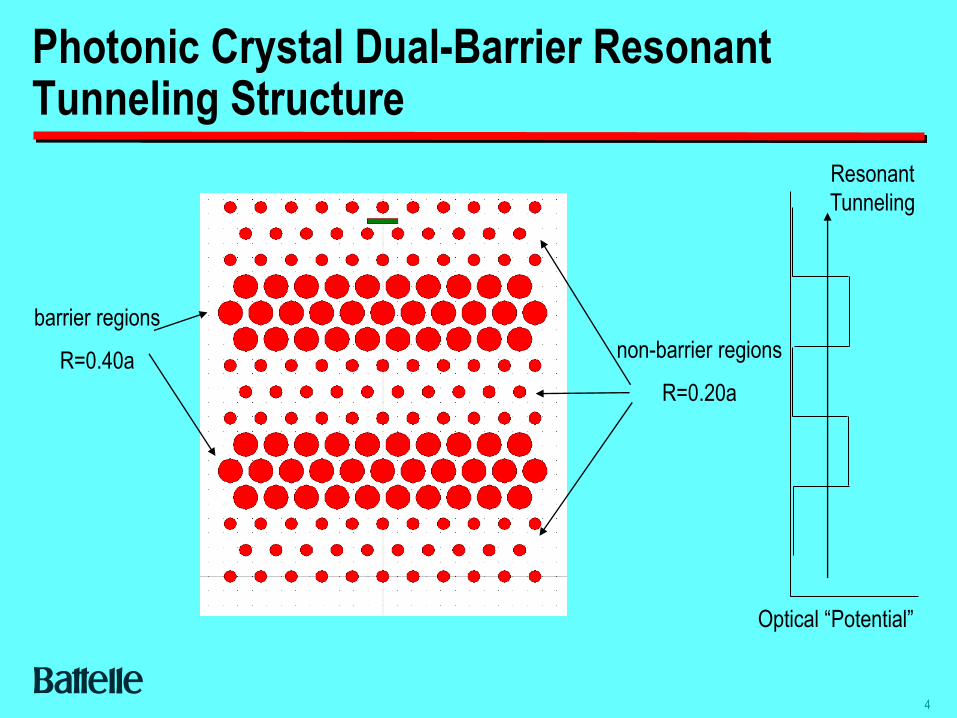
Photonic Crystal Dual-Barrier Resonant Tunneling Structure
non-barrier regions
R=0.20a
barrier regions
R=0.40a
Optical “Potential”
Resonant
Tunneling

5
Finite-Difference Time Domain Simulations of DBRT Structure
Resonant Wavelength Non-Resonant Wavelength
Same structure can be used for electro-optical modulation if
strong enough EO effect can be achieved.

6
Transmission Spectrum of DBRT Filter
Peak 1.52 mm
FWHM 20 nm SOI/air
Thickness = 1 mm
a=0.42 mm
R1=0.35a
R2=0.40a
TM polarization
7
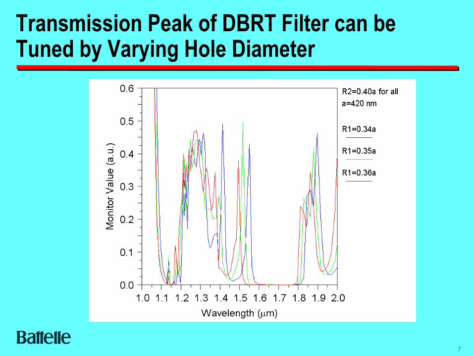
Transmission Peak of DBRT Filter can be Tuned by Varying Hole Diameter
8
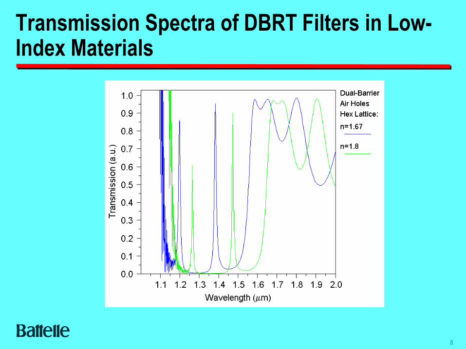
Transmission Spectra of DBRT Filters in Low-Index Materials

9
Coarse Wavelength Demultiplexer Based on DBRT Structures
l1 l2
l1, l2
barrier regions
R=R0
R=R1
R=R2
High loss limits the usefulness of the structure to a small number
of outputs.
10
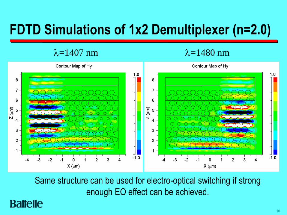
FDTD Simulations of 1x2 Demultiplexer (n=2.0)
l=1407 nm l=1480 nm
Same structure can be used for electro-optical switching if strong
enough EO effect can be achieved.

11
SEM of Silicon-on-Insulator DBRT Structure
12
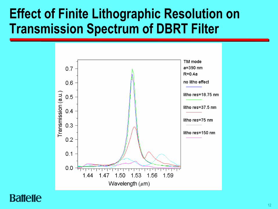
Effect of Finite Lithographic Resolution on Transmission Spectrum of DBRT Filter

13
Summary
Dual-barrier heterostructure is an alternative to photonic crystal slab devices based on line and point defects
Can be implemented in lower-index materials and thicker layers than PC slab waveguides
Structure is suitable for coarse WDM and EO modulators/switches
High fabrication quality is needed

14
Acknowledgements
Dr. Sajeev John (University of Toronto)
Dr. Phillip Fauchet et al. (University of Rochester)
Cornell Nanofabrication Facility
Copyright © 2022 FDOKUMEN