Time-resolved photoemission spectroscopy on a metal/ferroelectric heterostructure
Electrical spin injection from an organic-based ferrimagnet in
a hybrid organic/inorganic heterostructure
Lei Fang1*
, K. Deniz Bozdag1*
, Chia-Yi Chen2, P.A. Truitt
1, A. J. Epstein
1,3†and E.
Johnston-Halperin1†
1Department of Physics, The Ohio State University, Columbus, OH 43210-1117, USA
2Chemical Physics Program, The Ohio State University, Columbus, OH, 43210-1106,
USA 3Department of Chemistry, The Ohio State University, Columbus, OH 43210-1173,
USA
Abstract
We report the successful extraction of spin polarized current from the organic-based
room temperature ferrimagnetic semiconductor V[TCNE]x (x~2, TCNE:
tetracyanoethylene; TC ~ 400 K, EG ~ 0.5 eV, ~ 10-2
S/cm) and its subsequent injection
into a GaAs/AlGaAs light-emitting diode (LED). The spin current tracks the
magnetization of V[TCNE]x~2, is weakly temperature dependent, and exhibits heavy hole
/ light hole asymmetry. This result has implications for room temperature spintronics and
the use of inorganic materials to probe spin physics in organic and molecular systems.
The field of semiconductor spintronics promises the extension of spin-based
electronics beyond memory and magnetic sensing into active electronic components with
implications for next-generation computing [1] and quantum information [2]. The
development of organic-based magnets with room temperature magnetic ordering [3] and
semiconducting functionality [4] promises to further broaden this impact by providing a
route to all-organic spintronic devices [5-6] and hybrid organic/inorganic structures
capable of exploiting the multifunctionality [7-8] and ease of production in organic
systems [9] as well as the well established spintronic functionality of inorganic materials.
Our work demonstrates electrical spin injection in a hybrid organic/inorganic spin-
resolved light-emitting diode (spin-LED) [10] structure and opens the door to a new class
of active, hybrid spintronic devices with multifunctional behavior defined by the optical,
electronic and chemical sensitivity [11] of the organic layer. In addition, spin transport in
these hybrid structures provides the opportunity to use well-characterized inorganic
materials as a probe of spin physics in organic and molecular systems.
The magnetic order in V[TCNE]x~2 (TC ~ 400 K) originates from direct
antiferromagnetic exchange coupling between the unpaired spins of V2+
(t2g , S = 3/2) and
TCNE- (*
, S = 1/2). As shown in Fig. 1(a), the unpaired spin in the TCNE- anion is
distributed over the entire molecule [12] and occupies the * antibonding level. The *
orbital can accept another electron with opposite spin, which costs an additional Coulomb
energy [4, 13] Uc ~ 2 eV. Therefore, the * band is split into two oppositely spin
polarized subbands: occupied * and unoccupied *
+Uc. The t2g levels lie within the
Coulomb gap [14] and define the valence band while the * + Uc levels define the
conduction band with an 0.5 eV bandgap ( ~ 10-2
S/cm). This proposed electronic
structure with ferromagnetically aligned conduction and valance bands is consistent with
theoretical calculations [15-17] and experimental studies [5, 14, 18].
The implications of the electronic and magnetic structure of V[TCNE]x~2 for a spin-
LED device are depicted schematically in Fig. 1(b). Spin polarized carriers are extracted
from a spin-polarized source (V[TCNE]x~2 here) and injected into the conduction band of
the n-AlGaAs layer of an n-i-p diode with a GaAs quantum well (QW) embedded in the
intrinsic region. The sign and magnitude of the spin-polarized charge injection are
determined by the magnetization of the V[TCNE]x~2 and can be analyzed through the
polarization of the heavy-hole (HH) and light-hole (LH) electroluminescence (EL) from
carriers that relax into the quantum well. These optical polarizations have complementary
coupling to the spin polarization of the electron current [19], where the optical
polarization is defined as PEL = (IRCP
– ILCP
)/(IRCP
+ ILCP
) (IRCP
and ILCP
indicate the
intensity of right and left circular polarization, respectively). For example, an S = + 1/2
electron will yield an RCP photon on recombining with a HH and an LCP photon on
recombining with a LH. This asymmetry of HH and LH with a given magnetization of
the spin polarized source is shown schematically in Fig. 1(c) and can be resolved in EL
due to the energy difference between HH and LH states. Thus the optical polarization of
the EL is directly proportional the spin polarized current present in the V[TCNE]x~2.
The organic and inorganic layers of the spin-LED are synthesized using chemical
vapor deposition (CVD) and molecular beam epitaxy (MBE), respectively. The
AlGaAs/GaAs heterostructure follows previous spin-LED devices. The MBE grown III-
V material is grown on a p-doped (p = 1×10¹⁸
cm-3
) GaAs (100) substrate with layer
structure as follows: 300 nm p-GaAs (1×10¹⁷
cm-3
)/ 200 nm p-Al0.1Ga0.9As (p = 1×10¹⁶
cm-3
)/ 25 nm i-Al0.1Ga0.9As/ 10 nm i-GaAs/ 25 nm i-Al0.1Ga0.9As/ 100 nm n-Al0.1Ga0.9As
(n = 1×10¹⁶
cm-3
)/ 15 nm nn+Al0.1Ga0.9As, n = 1×10
16 cm
-3 to 5×10
18 cm
-3/ 15 nm n
+-
Al0.1Ga0.9As (n+ = 5×10
18 cm
-3) [20]. Devices are fabricated using standard
photolithography to define a mesa that is protected with photoresist except for a narrow
window (100 m by 1 mm). The V[TCNE]x~2 is deposited uniformly across the sample at
40 °C and 35 Torr in an argon glovebox [9]. The top electrical contact consists of an
optically transparent aluminium layer (7 nm) and a high conductivity gold layer (23 nm,
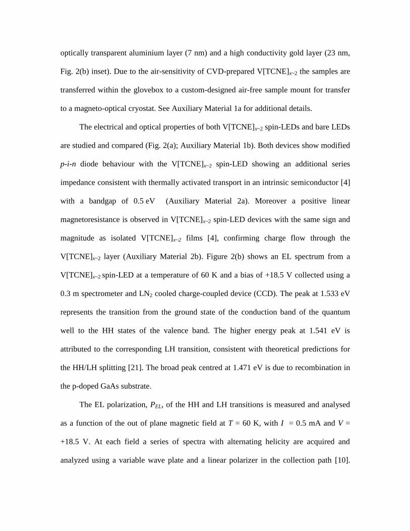
Fig. 2(b) inset). Due to the air-sensitivity of CVD-prepared V[TCNE]x~2 the samples are
transferred within the glovebox to a custom-designed air-free sample mount for transfer
to a magneto-optical cryostat. See Auxiliary Material 1a for additional details.
The electrical and optical properties of both V[TCNE]x~2 spin-LEDs and bare LEDs
are studied and compared (Fig. 2(a); Auxiliary Material 1b). Both devices show modified
p-i-n diode behaviour with the V[TCNE]x~2 spin-LED showing an additional series
impedance consistent with thermally activated transport in an intrinsic semiconductor [4]
with a bandgap of 0.5 eV (Auxiliary Material 2a). Moreover a positive linear
magnetoresistance is observed in V[TCNE]x~2 spin-LED devices with the same sign and
magnitude as isolated V[TCNE]x~2 films [4], confirming charge flow through the
V[TCNE]x~2 layer (Auxiliary Material 2b). Figure 2(b) shows an EL spectrum from a
V[TCNE]x~2 spin-LED at a temperature of 60 K and a bias of +18.5 V collected using a
0.3 m spectrometer and LN2 cooled charge-coupled device (CCD). The peak at 1.533 eV
represents the transition from the ground state of the conduction band of the quantum
well to the HH states of the valence band. The higher energy peak at 1.541 eV is
attributed to the corresponding LH transition, consistent with theoretical predictions for
the HH/LH splitting [21]. The broad peak centred at 1.471 eV is due to recombination in
the p-doped GaAs substrate.
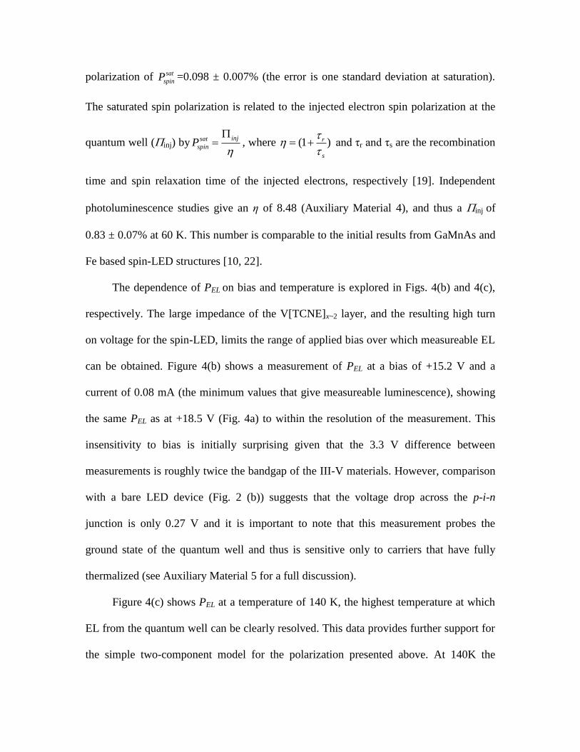
The EL polarization, PEL, of the HH and LH transitions is measured and analysed
as a function of the out of plane magnetic field at T = 60 K, with I = 0.5 mA and V =
+18.5 V. At each field a series of spectra with alternating helicity are acquired and
analyzed using a variable wave plate and a linear polarizer in the collection path [10].

IRCP
and ILCP
are determined individually by integrating over the appropriate spectral
peaks (highlighted regions in Fig. 2(b)) and PEL is calculated for the HH and LH,
respectively. In these spin-LED devices the total polarization signal is composed of four
independent contributions: the spin injection EL, the intrinsic magnetic field response of
the AlGaAs/GaAs quantum well (Zeeman effect) [22], magnetic circular dichroism
(MCD) from the cryostat windows, and MCD [10, 23-24] in the V[TCNE]x~2 layer.
Figures 3 (a) – (c) show cartoons explaining how these contributions combine to give the
total measured EL polarization while Figures 3 (d) – (f) show corresponding
experimental measurements of these effects.
Figure 3 (a) shows the expected linear response from both the Zeeman effect and
dichroism in the cryostat windows. In principle the HH should show a three times larger
Zeeman splitting than the LH due to their increased angular momentum (mj = 3/2 and mj
= 1/2, respectively); however this difference is not observed (Fig. 3 (d)), suggesting that
the dichroism of the cryostat windows is the dominant effect.
In Fig. 3 (b) the expected MCD response is plotted as the dashed gray line, with the
contribution from Fig. 3 (a) plotted as the dashed orange line. The total of these two
effects is shown as the green solid line, and qualitatively agrees with independent
measurements of the MCD shown in Fig. 3 (e). This data is collected by optically
exciting unpolarized carriers in the quantum well using a linearly polarized pump at
1.771 eV and a power density of 100 W/cm2. The resulting photoluminescence (PL)
exhibits both the linear window dichroism shown in Fig. 3(d) and saturation at ± 200 Oe,
consistent with the field dependence of the magnetization of V[TCNE]x~2 (Fig. 4(a),
green line; Auxiliary Material 3) as predicted in Fig. 3 (b). Note that the since the HH and

LH PL are so close in energy, there is no measureable difference between the HH and LH
MCD response.
Finally in Fig. 3 (c), the spin injection EL is added to the various background
signals shown in Figs. 3 (a) and (b) (green line). In contrast to these backgrounds, the
spin injection EL should have opposite sign for the HH and LH (red and blue dashed
lines, respectively). The total EL signal is given by HH
windowZeeman
HH
MCD
HH
spin
HH
EL PPPP
and LH
windowZeeman
LH
MCD
LH
spin
LH
EL PPPP for the HH and LH, respectively. Note that in the
case where the magnitude of the spin injection signal is comparable to that of the MCD
background the two terms that depend on the magnetization of the V[TCNE]x~2 cancel for
the LH, leaving a simple linear dependence due to Zeeman splitting and window
dichroism. Figure 3 (f) shows the total EL signal from a full V[TCNE]x~2 spin-LED
device. As expected, and in contrast to the background measurements in Figs. 3 (d) and
(e), a clear distinction between HH and LH polarization is observed and the linear
response of the LH indicates that at this temperature the spin injection signal and MCD
are of comparable magnitude.
The bare EL signal (Pbare) for both HH and LH transitions can be removed by a
linear fit to the calibration data in Fig. 3(d), leaving the corrected polarization
as / / /HH LH HH LH HH LH
EL MCD spinP P P . The background corrected polarization signals are plotted
in Fig. 4(a) where it can be seen that PEL of the HH peak reaches saturation at ~ 200 Oe,
closely tracking the out of plane magnetization of the V[TCNE]x~2 (Fig. 4(a) green line).
Moreover, subtracting LH
ELP from HH
ELP will result in a cancellation of the MCD terms and
give twice the optical polarization ( 2 spinP ). This analysis yields a saturated spin
polarization of sat
spinP =0.098 ± 0.007% (the error is one standard deviation at saturation).
The saturated spin polarization is related to the injected electron spin polarization at the
quantum well (inj) byinjsat
spinP
, where (1 )r
s
and τr and τs are the recombination
time and spin relaxation time of the injected electrons, respectively [19]. Independent
photoluminescence studies give an η of 8.48 (Auxiliary Material 4), and thus a inj of
0.83 ± 0.07% at 60 K. This number is comparable to the initial results from GaMnAs and
Fe based spin-LED structures [10, 22].
The dependence of PEL on bias and temperature is explored in Figs. 4(b) and 4(c),
respectively. The large impedance of the V[TCNE]x~2 layer, and the resulting high turn
on voltage for the spin-LED, limits the range of applied bias over which measureable EL
can be obtained. Figure 4(b) shows a measurement of PEL at a bias of +15.2 V and a
current of 0.08 mA (the minimum values that give measureable luminescence), showing
the same PEL as at +18.5 V (Fig. 4a) to within the resolution of the measurement. This
insensitivity to bias is initially surprising given that the 3.3 V difference between
measurements is roughly twice the bandgap of the III-V materials. However, comparison
with a bare LED device (Fig. 2 (b)) suggests that the voltage drop across the p-i-n
junction is only 0.27 V and it is important to note that this measurement probes the
ground state of the quantum well and thus is sensitive only to carriers that have fully
thermalized (see Auxiliary Material 5 for a full discussion).
Figure 4(c) shows PEL at a temperature of 140 K, the highest temperature at which
EL from the quantum well can be clearly resolved. This data provides further support for
the simple two-component model for the polarization presented above. At 140K the
magnitude for both HH
spinP and LH
spinP are reduced from 60K, consistent with an increased η of
18.09 (see Auxiliary Material 4) and consistent with literature reports of the decrease in
spin relaxation time at high temperature [25]. When this η is combined with sat
spinP = 0.036
± 0.006%, a value for inj (140 K) of 0.66 ± 0.16% is determined. This relatively modest
dependence on temperature (inj(60 K) = 0.83 ± 0.07%) is consistent with spin injection
from other room temperature ferromagnets such as Fe [24][26][27].
In conclusion, optical detection of electrical spin injection across a
V[TCNE]x~2/AlGaAs interface has been demonstrated using an active hybrid
organic/inorganic spin-LED device. We report circular polarization of the
electroluminescence that tracks the magnetization of the V[TCNE]x~2 layer and exhibits
HH/LH asymmetry. These studies validate the spintronic functionality of organic-based
magnets, laying the foundation for a new class of multifunctional hybrid spintronic
structures and representing the first all-semiconductor spintronic device with the potential
for room temperature operation. Moreover, we establish the technique of using
extensively studied inorganic heterostructures as a sensitive probe of free carrier spin
physics in organic and molecular systems.
We acknowledge Dr. Mark Brenner and Semiconductor Epitaxial and Analysis
Laboratory (SEAL) of the Ohio State University for providing AlGaAs/GaAs quantum
well LED detector. We also acknowledge discussions and interactions with J. A. Gupta,
R. Myers and J. -W. Yoo. This work was supported by the NSF MRSEC program (DMR-
0820414), OSU-Institute of Material Research and DOE – spin (DE-FG02-01ER45931).
References
* These authors contributed equally to this work
†To whom correspondence should be addressed. E-mail: [email protected]
state.eduand [email protected].
[1] International technology roadmap for semiconductors. Executive summary for
2009. (2009).
[2] D. P. Divincenzo, Science 270, 255 (1995).
[3] J. M. Manriquez et al., Science 252, 1415 (1991).
[4] V. N. Prigodin et al., Adv. Mater. 14, 1230 (2002).
[5] J.-W. Yoo et al., Nat. Mater. 9, 638 (2010).
[6] J.-W. Yoo et al., Phys. Rev. B. 80, 205207 (2009).
[7] J.-W. Yoo et al., Phys. Rev. Lett. 97, 247205 (2006).
[8] K. Deniz Bozdag et al., Phys. Rev. B. 82, 094449 (2010)
[9] K. I. Pokhodnya, A. J. Epstein, and J. S. Miller, Adv. Mater. 12, 410 (2000).
[10] Y. Ohno et al., Nature 402, 790 (1999).
[11] J. S. Miller and A. J. Epstein, Angew. Chem. Int. Edit. 33, 385 (1994).
[12] A. Zheludev et al., J. Am. Chem. Soc. 116, 7243 (1994).
[13] C. Tengstedt et al., Phys. Rev. B. 69, 165208 (2004).
[14] C. Tengstedt et al., Phys. Rev. Lett. 96, 057209 (2006).
[15] A. L. Tchougreeff and R. Dronskowski, J. Comput. Chem. 29, 2220 (2008).
[16] H. Matsuura, K. Miyake, and H. Fukuyama, J. Phys. Soc. Jpn. 79, 034712 (2010).
[17] G. C. De Fusco et al., Phys. Rev. B. 79, 085201 (2009).
[18] J. B. Kortright et al., Phys. Rev. Lett. 100, 257204 (2008).
[19] F. Meier and B. P. Zakharchenya, Optical Orientation Amsterdam, The
Netherlands: North-Holland, vol. 8. (1984).
[20] C. Adelmann et al., Phys. Rev. B. 71, 121301(R) (2005)
[21] B. Jonker, Proc. IEEE. 91, 727 (2003).
[22] H. Zhu et al., Phys. Rev. Lett. 87, 016601 (2001).
[23] X. Y, Dong et al., Appl. Phys. Lett. 86, 102107 (2005).
[24] A. T. Hanbicki et al., Appl. Phys. Lett. 80, 1240 (2002).
[25] J. M. Kikkawa and D. D. Awschalom, Phys. Rev. Lett. 80, 4313 (1998)
[26] The spin injection efficiency tracks with the bulk magnetization, and is distinct
from materials such as LSMO [27] where surface relaxation leads to a rapid
depolarization of the spin current at elevated temperature.
[27] J.-H. Park et al., Phys. Rev. Lett. 81,1953 (1998)
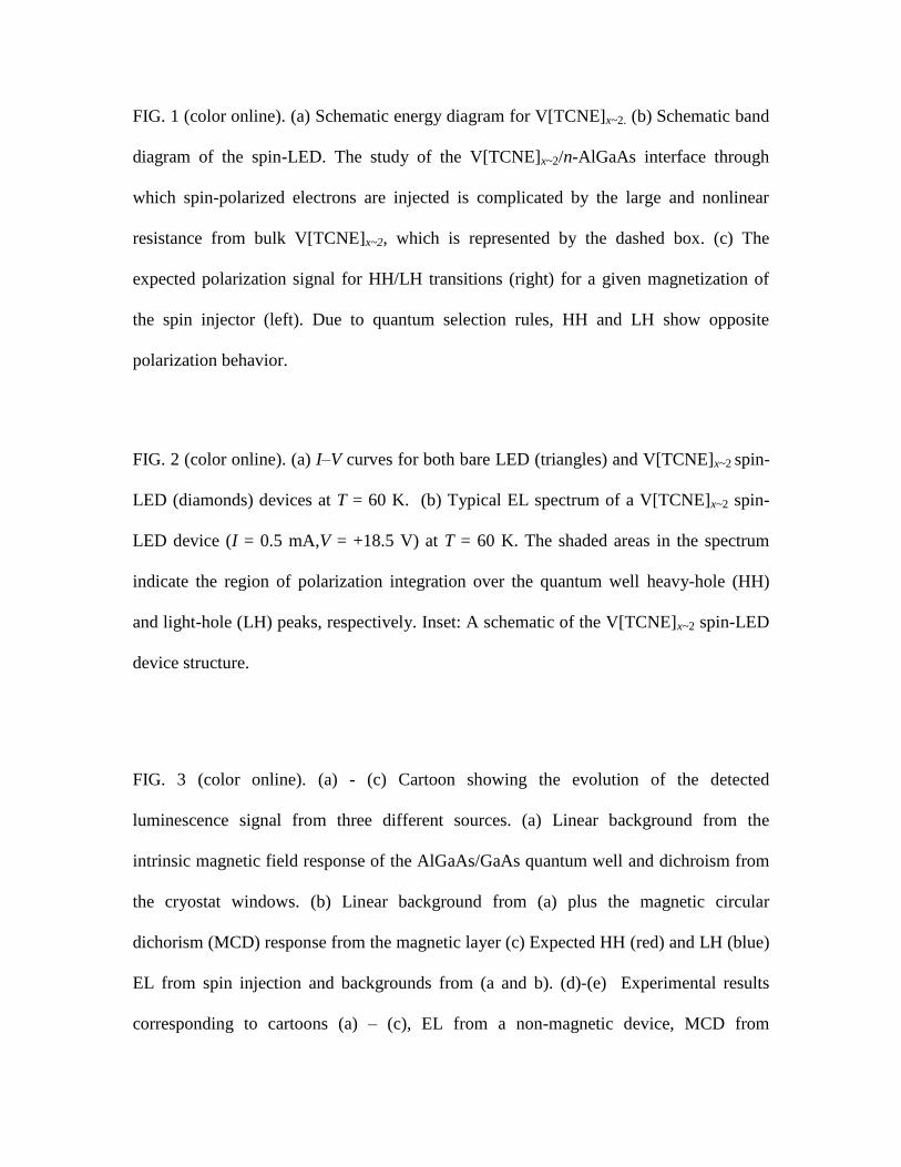
FIG. 1 (color online). (a) Schematic energy diagram for V[TCNE]x~2. (b) Schematic band
diagram of the spin-LED. The study of the V[TCNE]x~2/n-AlGaAs interface through
which spin-polarized electrons are injected is complicated by the large and nonlinear
resistance from bulk V[TCNE]x~2, which is represented by the dashed box. (c) The
expected polarization signal for HH/LH transitions (right) for a given magnetization of
the spin injector (left). Due to quantum selection rules, HH and LH show opposite
polarization behavior.
FIG. 2 (color online). (a) I–V curves for both bare LED (triangles) and V[TCNE]x~2 spin-
LED (diamonds) devices at T = 60 K. (b) Typical EL spectrum of a V[TCNE]x~2 spin-
LED device (I = 0.5 mA,V = +18.5 V) at T = 60 K. The shaded areas in the spectrum
indicate the region of polarization integration over the quantum well heavy-hole (HH)
and light-hole (LH) peaks, respectively. Inset: A schematic of the V[TCNE]x~2 spin-LED
device structure.
FIG. 3 (color online). (a) - (c) Cartoon showing the evolution of the detected
luminescence signal from three different sources. (a) Linear background from the
intrinsic magnetic field response of the AlGaAs/GaAs quantum well and dichroism from
the cryostat windows. (b) Linear background from (a) plus the magnetic circular
dichorism (MCD) response from the magnetic layer (c) Expected HH (red) and LH (blue)
EL from spin injection and backgrounds from (a and b). (d)-(e) Experimental results
corresponding to cartoons (a) – (c), EL from a non-magnetic device, MCD from

photoluminescence and EL from a spin-LED, respectively. Filled symbols are for field
sweeping up and open symbols are for field sweeping down. Note that a field-
independent offset is subtracted from all scans. Error bars are determined using the
standard deviation of multiple measurements at each field value.
FIG. 4(color online).Circular polarization for HH and LH transitions in a V[TCNE]x~2
spin-LED device at (a) T = 60 K, I = 0.5 mA and V = +18.5 V, (b) T = 60 K, I = 0.08 mA
and V = +15.2 V and (c) T = 140 K, I = 1.5 mA and V = +10.1 V (red and blue symbols
for HH and LH, respectively). The solid green line in (a) represents out of plane
magnetization of the V[TCNE]x~2 layer. Error bars are determined as in Fig. 3 except for
(b), where the long measurement time required for low bias measurements prevents
statistically significant averaging. As a result, the error is estimated from the scatter of the
LH data.
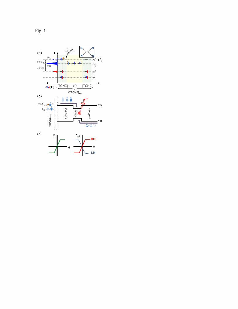
Fig. 1.

Fig. 2
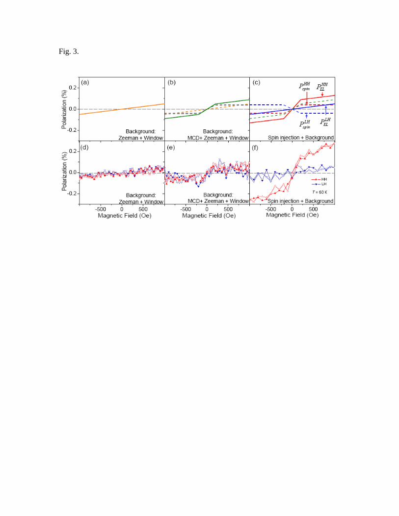
Fig. 3.
Fig. 4.
Copyright © 2022 FDOKUMEN