Electronic and electrical properties of functional interfaces studied by hard X-ray photoemission

Time-resolved PhotoEmission Spectroscopy on a Metal/Ferroelectric Heterostructure
J. E. Rault,1, ∗ G. Agnus,2 T. Maroutian,2 V. Pillard,2 Ph. Lecoeur,2 G.
Niu,3, † B. Vilquin,3 M. G. Silly,4 A. Bendounan,4 F. Sirotti,4 and N. Barrett1, ‡
1CEA, DSM/IRAMIS/SPCSI, F-91191 Gif-sur-Yvette Cedex, France2Institut d’Electronique Fondamentale, Univ Paris-Sud, CNRS UMR 8622, 91405 Orsay Cedex, France
3Universite de Lyon, Ecole Centrale de Lyon, Institut des Nanotechnologies de Lyon, F-69134 Ecully cedex, France4Synchrotron-SOLEIL, BP 48, Saint-Aubin, F91192 Gif sur Yvette CEDEX, France
In thin film ferroelectric capacitor the chemical and electronic structure of the electrode/FEinterface can play a crucial role in determining the kinetics of polarization switching. We investigatethe electronic structure of a Pt/BaTiO3/SrTiO3:Nb capacitor using time-resolved photoemissionspectroscopy. The chemical, electronic and depth sensitivity of core level photoemission is usedto probe the transient response of different parts of the upper electrode/ferroelectric interface tovoltage pulse induced polarization reversal. The linear response of the electronic structure agreesquantitatively with a simple RC circuit model. The non-linear response due to the polarizationswitch is demonstrated by the time-resolved response of the characteristic core levels of the electrodeand the ferroelectric. Adjustment of the RC circuit model allows a first estimation of the Pt/BTOinterface capacitance. The experiment shows the interface capacitance is at least 100 times higherthan the bulk capacitance of the BTO film, in qualitative agreement with theoretical predictionsfrom the literature.
PACS numbers: 77.80.-e 73.21.Ac 73.40.-c 77.84.-s
I. INTRODUCTION
Epitaxially strained oxide thin films make ferroelec-tric (FE) based heterostructures of real interest for newelectronic devices1,2. High read and write speeds are ofprime importance for implementing ferroelectric basedelectronics. The dynamic process of polarization reversalis crucial to understand the application limits in terms ofmaximum frequency and long-term fatigue3. It is there-fore essential to understand the polarization switchingkinetics in thin film ferroelectric capacitor structures.
Polarization reversal in the prototypical BaTiO3 ferro-electric singles crystals was first studied by W.J. Merz4.The switching dynamics have been described by classicalnucleation theory of Kolmogorov, Avrami and Ishibashiin which the polarization is reversed first by domain nu-cleation then domain wall motion5–7. In smaller capac-itive stuctures, nucleation limited switching have beenfound to provide a more accurate description8–10. Fol-lowing the model of Merz, the switching time dependsexponentially on the activation field4. Gruverman et al.have shown that there are high and low field regimes forpolarization reversal. Small capacitive structures undera high field switch more rapidly whereas larger area ca-pacitors switch more quickly under low fields because thekinetics are nucleation limited9.
Most characterization of FE switching has been doneusing electrical methods but accurate switching measure-ments are often limited by the RC circuit load on thedevice and parasitic resistances. Despite this problem,it has been shown that the activation field can be de-termined independently of the RC circuit characteristics,
the effect of the latter being a time dilation of the FEswitch11.
The properties of the electrode/FE interface may alsodetermine the switching kinetics. For example, it hasbeen suggested that defect related local fields determinethe switching time in BiFeO3 capacitors12. At the elec-trode/FE interface, chemistry, strain and electronic or-dering combine in a complex way to screen the inter-face polarization charge of the ferroelectric layer. An ac-curate description of the dynamical electronic structuremay help to better understand the switching process andthe phenomena underlying the results of electrical mea-surements. However, experimental data on the electronicproperties of such systems are scarce, principally due tothe intrinsic difficulty of measuring a buried interface.
The use of complementary in-operando, i.e. submit-ted to a realistic voltage excitation, structural character-ization techniques is therefore desirable. Ideally, thesetechniques should be independent of the electrical cir-cuit required to switch the polarization. For instance,Gorfman et al. used time-resolved x-ray diffraction todetermine the lattice dynamics and atomic positions inpiezoelectrics13.
X-ray photoemission spectroscopy (XPS) is a power-ful, direct tool for characterizing the chemical and elec-tronic interface structure. It has been used with in-situ bias to demonstrate the migration of oxygen va-cancies in Pt/HfO2
14 or to conduct impedance-like mea-surements on Rb deposited on silicon15. Chen andKlein used in-situ photoemission spectroscopy on a BTOmonocristal to deduce the barriers properties as a func-tion of ferroelectric polarization16. Our group studieda Pt/BaTiO3/Nb:SrTiO3 (Pt/BTO/NSTO) heterostruc-
arX
iv:1
307.
3769
v1 [
cond
-mat
.mtr
l-sc
i] 1
4 Ju
l 201
3
2
ture with bias application and found polarization de-pendent barriers and a non-trivial behavior of the core-levels as a function of applied bias17. All of these studiesshow the potential of photoemission experiments for in-operando work.
An exciting route for a fundamental understanding ofthe interface electronic structure of FE devices wouldtherefore be time-resolved photoelectron spectroscopy.State-of-the-art delay-line detectors allow detection ofphotoemitted electrons with a time-resolution down to5 to 10 ns18. Although switching times can be of the or-der of a nanosecond19, in many cases it may be sufficientto resolve the transient response of the electronic struc-ture to the applied voltage pulse. The aim is to detailthe transient response of the electronic structure to theswitching pulse and the role of the interface and bulk filmcapacitance in defining ultimate device speed.
We investigate the electronic structure of an elec-trode/FE interface using time-resolved photoemissionspectroscopy. The static properties of the ferroelec-tric capacitance have been studied by photoemission inRef. 17. Bias pulses on a Pt/BTO/NSTO capacitorprobe the time-resolved chemical and electronic structureof the Pt/BTO interface. An equivalent circuit model isused predicting a behavior which compares well with thephotoemission results on the real system. This shows thepotential of time-resolved photoemission spectroscopy tofollow the chemical/electronic changes in working modelFE microelectronic devices.
II. EXPERIMENT
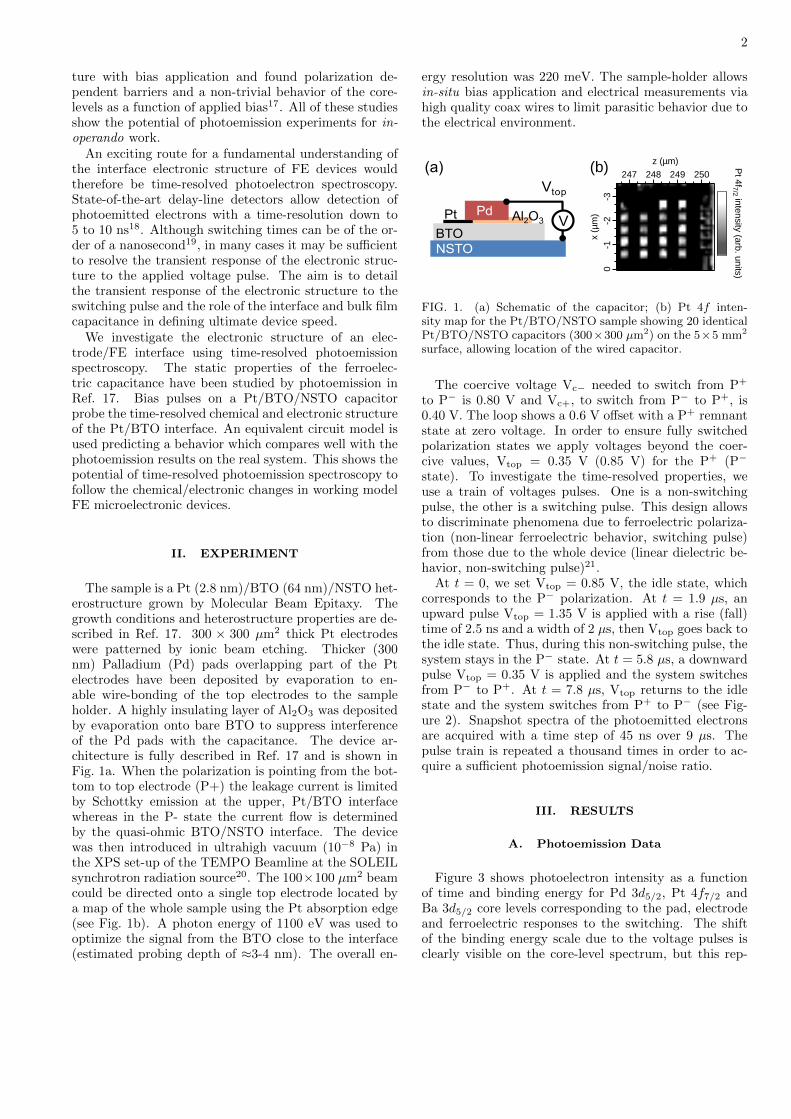
The sample is a Pt (2.8 nm)/BTO (64 nm)/NSTO het-erostructure grown by Molecular Beam Epitaxy. Thegrowth conditions and heterostructure properties are de-scribed in Ref. 17. 300 × 300 µm2 thick Pt electrodeswere patterned by ionic beam etching. Thicker (300nm) Palladium (Pd) pads overlapping part of the Ptelectrodes have been deposited by evaporation to en-able wire-bonding of the top electrodes to the sampleholder. A highly insulating layer of Al2O3 was depositedby evaporation onto bare BTO to suppress interferenceof the Pd pads with the capacitance. The device ar-chitecture is fully described in Ref. 17 and is shown inFig. 1a. When the polarization is pointing from the bot-tom to top electrode (P+) the leakage current is limitedby Schottky emission at the upper, Pt/BTO interfacewhereas in the P- state the current flow is determinedby the quasi-ohmic BTO/NSTO interface. The devicewas then introduced in ultrahigh vacuum (10−8 Pa) inthe XPS set-up of the TEMPO Beamline at the SOLEILsynchrotron radiation source20. The 100×100 µm2 beamcould be directed onto a single top electrode located bya map of the whole sample using the Pt absorption edge(see Fig. 1b). A photon energy of 1100 eV was used tooptimize the signal from the BTO close to the interface(estimated probing depth of ≈3-4 nm). The overall en-
ergy resolution was 220 meV. The sample-holder allowsin-situ bias application and electrical measurements viahigh quality coax wires to limit parasitic behavior due tothe electrical environment.
Pt
BTONSTO
PdV
Vtop
Al2O3
(a)
-3-2
-10
x (µ
m)
250249248247
z (µm) Pt 4f7/2 intensity (arb. units)
(b)
FIG. 1. (a) Schematic of the capacitor; (b) Pt 4f inten-sity map for the Pt/BTO/NSTO sample showing 20 identicalPt/BTO/NSTO capacitors (300×300 µm2) on the 5×5 mm2
surface, allowing location of the wired capacitor.
The coercive voltage Vc− needed to switch from P+
to P− is 0.80 V and Vc+, to switch from P− to P+, is0.40 V. The loop shows a 0.6 V offset with a P+ remnantstate at zero voltage. In order to ensure fully switchedpolarization states we apply voltages beyond the coer-cive values, Vtop = 0.35 V (0.85 V) for the P+ (P−
state). To investigate the time-resolved properties, weuse a train of voltages pulses. One is a non-switchingpulse, the other is a switching pulse. This design allowsto discriminate phenomena due to ferroelectric polariza-tion (non-linear ferroelectric behavior, switching pulse)from those due to the whole device (linear dielectric be-havior, non-switching pulse)21.
At t = 0, we set Vtop = 0.85 V, the idle state, whichcorresponds to the P− polarization. At t = 1.9 µs, anupward pulse Vtop = 1.35 V is applied with a rise (fall)time of 2.5 ns and a width of 2 µs, then Vtop goes back tothe idle state. Thus, during this non-switching pulse, thesystem stays in the P− state. At t = 5.8 µs, a downwardpulse Vtop = 0.35 V is applied and the system switchesfrom P− to P+. At t = 7.8 µs, Vtop returns to the idlestate and the system switches from P+ to P− (see Fig-ure 2). Snapshot spectra of the photoemitted electronsare acquired with a time step of 45 ns over 9 µs. Thepulse train is repeated a thousand times in order to ac-quire a sufficient photoemission signal/noise ratio.
III. RESULTS
A. Photoemission Data
Figure 3 shows photoelectron intensity as a functionof time and binding energy for Pd 3d5/2, Pt 4f7/2 andBa 3d5/2 core levels corresponding to the pad, electrodeand ferroelectric responses to the switching. The shiftof the binding energy scale due to the voltage pulses isclearly visible on the core-level spectrum, but this rep-

3
1.6
1.2
0.8
0.4
0.0
Vto
p (V
)
9630Time (µs)
BTO
NSTO
Pt
BTO
NSTO
PtP-
P+
Vc+
Vc-
FIG. 2. Vtop pulse train as a function of time. The first pulseis non-switching P− to P−, the second is switching P− to P+
then back to P−. The BTO film is in the P+ state betweent = 5.8 µs and t = 7.8 µs. The coercive voltages Vc+ and Vc−are indicated by dotted lines.
1.35
0.85
0.35
Vto
p (V
)
781
779B
E (eV
)
Ba 3d5/2
1.35
0.85
0.35
Vto
p (V
) 72.5
70.5
BE
(eV)
Pt 4f7/2
9630Time (µs)
1.35
0.85
0.35
Vto
p (V
) 337
335
BE
(eV)
Pd 3d5/2
FIG. 3. Photoemitted electron intensity as a function of timeand binding energy (BE) for the three core-levels Pd 3d5/2,Pt 4f7/2 and Ba 3d5/2. The blue dotted curve shows the pulsetrain applied on the top electrode.
resentation is not well-suited for further analysis. Weused a fitting procedure which subtracts the secondaryelectron background and fits the instantaneous spectrumto a Gaussian shape for each time step. It returns thebinding energy position of the peak as a function of timeand allows a proper comparison of core-level responseto the electrical excitation. The width of each peak iskept constant after a preliminary fit procedure using ahigh-resolution reference spectrum taken with both elec-trodes grounded. The shape for all core-levels did notchange with time except for the spectra close to the rise
and fall of the bias pulses. At these moments, the peaksare highly distorted leading to spikes (typical width of150 ns) in the time-dependent binding-energy curves. Atypical spectrum far from the spikes is shown in Fig-ure 4 together with the fit. Doniach-Sunjic lineshapesare more suited to metallic peaks22, however, since we ex-tract binding energy differences between identical peaks(in shape) at different time, the use of Gaussian shape is agood approximation and leads to a less time-consumingprocedure. We used one component to fit the Ba 3dspectrum though it is known that two components areobserved at the Pt/BTO interface17. However, the sig-nal/noise ratio of the Ba core-level from the buried in-terface was not sufficient to properly fit two componentsat every time step (Fig. 4b).
Inte
nsity
(ar
b. u
nits
)
104010351030Kinetic Energy (eV)
Pt 4f (a)
Inte
nsity
(ar
b. u
nits
)
338334330326322Kinetic Energy (eV)
Ba 3d5/2(b)
FIG. 4. Example of spectrum of (a) Pt 4f and (b) Ba 3d5/2core-level taken at one time step (black circles) after subtrac-tion of a linear background. The Gaussian fitting lineshapeis shown in plain red.
Figure 5 shows the time dependence of the bindingenergies obtained from the fitting procedure. All spec-tra are referenced relative to their binding energy in theidle state at Vtop = 0.85 V. As expected, for the upward(downward) pulse, every core-level shows a decrease (in-crease) in binding energy due to the more positive (nega-tive) voltage applied on the top electrode in comparisonto the idle state. At every pulse rise and fall, spikes areobserved in the binding energy. This is likely to be due toa parasitic capacitance with a very small time-constantalthough we cannot single out its location in the circuit.A capacitance with a time-constant below the rise time ofthe generator will act as a differentiator, i.e. will differen-tiate the signal with respect to time. The time derivativeof a step pulse is the delta function we observe as binding

4
energy spikes here. Within the framework of the domainnucleation-domain switching model, Merz distinguishedthe lead current due to rapid domain nucleation from thecurrent due to domain wall motion and domain switch-ing. Rapid domain nucleation should therefore give riseto a current spike, whereas the response due to domainswitching should be broader. Therefore, the core levelbinding energy spike may also be tentatively correlatedwith the onset of domain nucleation.
For the non-switching pulse, the core-levels reach asteady state value before the end of the pulse. While Pdfollows quite closely the amplitude of the source pulse(∆BE = 0.4 eV compared to a pulse ∆V of 0.5 V), Ptand Ba only shift by 0.20 eV. For the P− to P+ pulse,the core-level shifts have a higher time constant and eachcore-level shift is quantitatively different. The ∆BE val-ues for the Pd, Pt and Ba core levels after 2 µs are 0.25,0.37 and 0.50 eV respectively. It is therefore clear that asimple electrostatic model is not sufficient to describe thePt/BTO interface and that the response of the electronicstructure to switches in polarization is non-linear.
B. Simulations
We conducted numerical simulations of the time-dependent linear behavior of the capacitor using PSpicesoftware23. This software can simulate the electrical re-sponse of a circuit under a pulse excitation. An upward(downward) pulse identical to the experimental one wasused and the circuit response in terms of the potentialdrop across each component calculated. We assume theresistances between the pulsed source and the palladiumpad (source impedance, RSP) and between the palladiumpad and the platinum electrode (imperfect metal/metalcontact, RPP) are ohmic. The resistance values shouldnot change with ferroelectric switching and are thereforekept constant. The Pt/BTO/NSTO stack is modeled bya RC circuit of resistance R and capacitance C and oftime constant τ = RC. The Pt 4f7/2 core-level is there-fore a direct probe of the voltage across the capacitor.An RC model accounts for the linear dielectric proper-ties but cannot of course directly model the FE switching,intrinsically non-linear. We have therefore used R and Cas fitting parameters that change in response to polariza-tion switch. Figure 6 displays the equivalent circuit usedin the simulations. The values which give the best fit toexperimental data are given in Table I for each polariza-tion state and the results of the simulation are shown inFigure 7.
We first discuss the behavior of the Pt and Pd core-levels. It was not possible to properly fit the photoemis-sion data without changing the resistance RSP betweenthe palladium pad and the pulse generator. Indeed, whenthe load (here the Pd/Pt/BTO/NSTO capacitor) on thepulse generator is too small (this is the case during thenon-switching pulse), the source is not able to deliverthe full pulse magnitude. In the framework of our simple
Vtop = 0.35 V Vtop = 0.85 V(P+) (P−)
RSP (Ω) 100 210RPP (Ω) 280 280R (Ω) 2200 350C (nF) 2.3 1.5τ (µs) 5 0.5
TABLE I. Best fit values for the components of the equivalentcircuit of Figure 7, for suffixes refer to text.
model, this results in two different values for RSP.With impedance matching taken into account, the
model circuit fits well the experimental values of thenon-switching pulse. The steady state low R is consis-tent with the high-current measured by static electri-cal experiment17. For the switching pulse P− to P+,the Pt/BTO/NSTO stack resistance R, is higher, con-sistent with the lower current through the capacitormeasured in Ref. 17. The high to low current behav-ior when switching from P− to P+ is due to the in-crease of the electron barrier height at the bottom in-terface (BTO/NSTO) of the capacitor (see Figure 7 ofRef. 17 for the polarization-dependent band lineups ofthe Pt/BTO/NSTO heterostructure).
Turning now to the transient behaviour, for the non-switching pulse P− to P−, both rise (charge) and fall(discharge) sequence fits well the experimental bindingenergy shifts. However, for the P− to P+ pulse, althoughthe P+ simulation curve fits well the rising edge of thecore level binding energies, it does not reproduce at allthe falling edge because of the time-resolution of our ex-periment compared with the electron dynamics of po-larization switching. At the end of the downward pulse,when the voltage goes from Vtop = 0.35 V back to 0.85 V,the BTO film switches back to the P− state. The dy-namic of polarization switching in thin films can be inthe nanosecond range depending on the pulse character-istics8, the ferroelectric layer properties24 and the elec-trodes12. This is faster than our time resolution so that,with respect to the spectral acquisition time, the stackinstantaneously switches to the P− state at t = 7.8 µs.The simulation of the P+ to P- switch in Fig. 7 is cal-culated from the parameters obtained for the P+ statewhich predict a time constant ten times larger than forthe P− state. Figure 8 shows a close-up of the switch backto P− following the P+ pulse. When the parameters ofthe P− steady state are used the fit is much better, re-producing quantitatively the experimental data (red linefor Pt 4f7/2, black line for Pd 3d5/2 on Fig. 8). The timeconstant of the RC component (τ = RC) estimated fromthe steady state fit parameters is 0.5 µs (5 µs) for the P−
(P+) state.The switching time is therefore sub-µs, in agreement
with literature9,19,25. The much higher value of τ de-duced from the steady P+ state may well reflect the RCcircuit load rather than a material property.
The simulation of the binding-energy response of the

5
-0.4
0.0
0.4 BE
shift (eV)
9630Time (µs)
1.35
0.85
0.35
Vto
p (V
)
FIG. 5. Time-dependent evolution of the binding energy (BE) shifts for the Pd 3d5/2 (blue circles), Pt 4f7/2 (green squares)and Ba 3d5/2 (red diamonds). The blue dotted curve shows the pulse train applied on the top electrode.
+
-
Pd Pt
RSP RPP
R
C
FIG. 6. Equivalent circuit used in the PSpice simulation soft-ware. The components values are summarized in Table I.
-0.6
-0.4
-0.2
0.0
0.2
0.4
0.6
BE
shi
ft (e
V)
9630Time (µs)
Pd 3d5/2 (exp.) Pd 3d5/2 (sim.)
Pt 4f7/2 (exp.) Pt 4f7/2 (sim.)
FIG. 7. Results of the electrical simulations (plain lines) ofthe experimental Pd 3d5/2 (blue circles) and Pt 4f7/2 (greensquares) evolution. The simulated curves are generated fromthe parameters of P− (Table I, right column) from t = 0to t = 5.8 µs and from the parameters of P+ (Table I, leftcolumn) from t = 5.8 to t = 9.2 µs.
barium core-level is more complex because it cannot eas-ily be related to a well-defined probing point in the model
0.6
0.4
0.2
0.0
BE
shi
ft (e
V)
987Time (µs)
FIG. 8. Results of the electrical simulations for the fall se-quence of the P− to P+ pulse. Pd 3d5/2 and Pt 4f7/2 exper-imental binding energy are shown in blue circles and greensquares respectively. The simulated plain curves of the fallsequence are generated from the parameters of the P− state(black line for Pd 3d5/2, red line for Pt 4f7/2). The simulated
dotted curves are generated from the parameters of the P+
state.
+
-
Pd Pt
Ba
RSP RPP
Rint
Rbulk
C
Cint
FIG. 9. Capacitance model for modeling the barium core-levelbehavior.
circuit. The model must account for the polarization-
6
-0.6
-0.4
-0.2
0.0
0.2
0.4
0.6B
E s
hift
(eV
)
9630Time (µs)
Ba 3d5/2 (exp.) Cint = 100 nF Cint = 0.5 nF
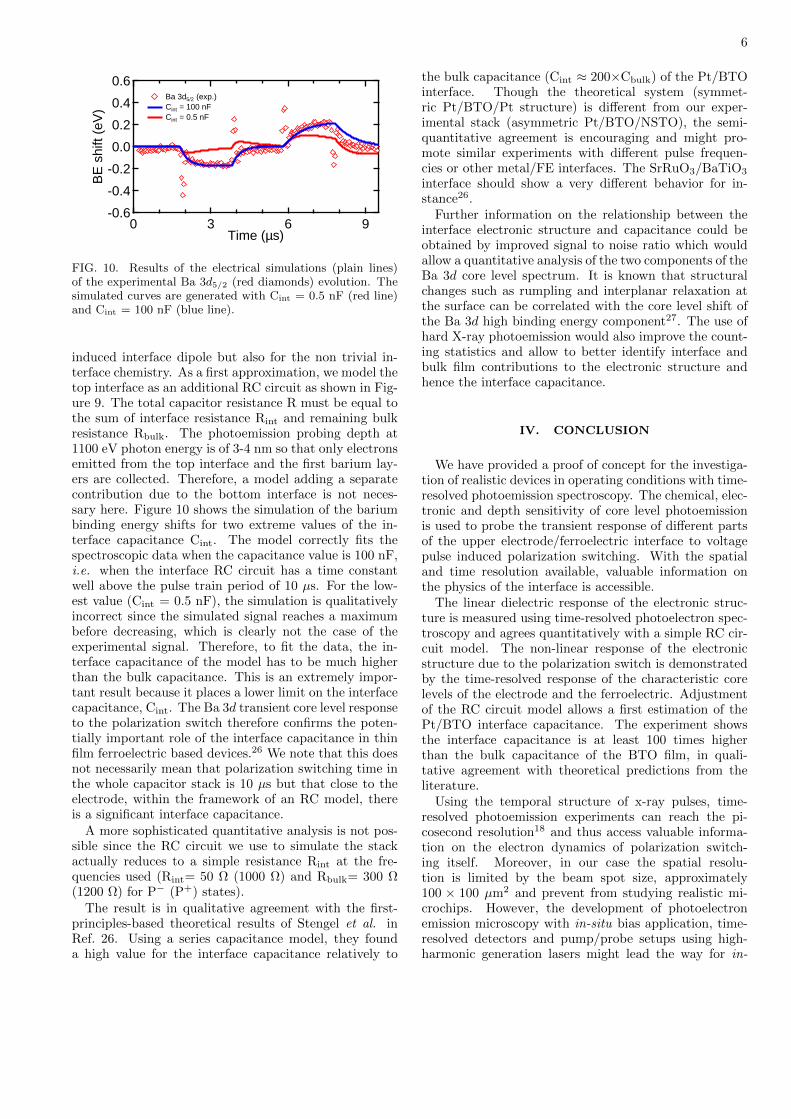
FIG. 10. Results of the electrical simulations (plain lines)of the experimental Ba 3d5/2 (red diamonds) evolution. Thesimulated curves are generated with Cint = 0.5 nF (red line)and Cint = 100 nF (blue line).
induced interface dipole but also for the non trivial in-terface chemistry. As a first approximation, we model thetop interface as an additional RC circuit as shown in Fig-ure 9. The total capacitor resistance R must be equal tothe sum of interface resistance Rint and remaining bulkresistance Rbulk. The photoemission probing depth at1100 eV photon energy is of 3-4 nm so that only electronsemitted from the top interface and the first barium lay-ers are collected. Therefore, a model adding a separatecontribution due to the bottom interface is not neces-sary here. Figure 10 shows the simulation of the bariumbinding energy shifts for two extreme values of the in-terface capacitance Cint. The model correctly fits thespectroscopic data when the capacitance value is 100 nF,i.e. when the interface RC circuit has a time constantwell above the pulse train period of 10 µs. For the low-est value (Cint = 0.5 nF), the simulation is qualitativelyincorrect since the simulated signal reaches a maximumbefore decreasing, which is clearly not the case of theexperimental signal. Therefore, to fit the data, the in-terface capacitance of the model has to be much higherthan the bulk capacitance. This is an extremely impor-tant result because it places a lower limit on the interfacecapacitance, Cint. The Ba 3d transient core level responseto the polarization switch therefore confirms the poten-tially important role of the interface capacitance in thinfilm ferroelectric based devices.26 We note that this doesnot necessarily mean that polarization switching time inthe whole capacitor stack is 10 µs but that close to theelectrode, within the framework of an RC model, thereis a significant interface capacitance.
A more sophisticated quantitative analysis is not pos-sible since the RC circuit we use to simulate the stackactually reduces to a simple resistance Rint at the fre-quencies used (Rint= 50 Ω (1000 Ω) and Rbulk= 300 Ω(1200 Ω) for P− (P+) states).
The result is in qualitative agreement with the first-principles-based theoretical results of Stengel et al. inRef. 26. Using a series capacitance model, they founda high value for the interface capacitance relatively to
the bulk capacitance (Cint ≈ 200×Cbulk) of the Pt/BTOinterface. Though the theoretical system (symmet-ric Pt/BTO/Pt structure) is different from our exper-imental stack (asymmetric Pt/BTO/NSTO), the semi-quantitative agreement is encouraging and might pro-mote similar experiments with different pulse frequen-cies or other metal/FE interfaces. The SrRuO3/BaTiO3
interface should show a very different behavior for in-stance26.
Further information on the relationship between theinterface electronic structure and capacitance could beobtained by improved signal to noise ratio which wouldallow a quantitative analysis of the two components of theBa 3d core level spectrum. It is known that structuralchanges such as rumpling and interplanar relaxation atthe surface can be correlated with the core level shift ofthe Ba 3d high binding energy component27. The use ofhard X-ray photoemission would also improve the count-ing statistics and allow to better identify interface andbulk film contributions to the electronic structure andhence the interface capacitance.
IV. CONCLUSION
We have provided a proof of concept for the investiga-tion of realistic devices in operating conditions with time-resolved photoemission spectroscopy. The chemical, elec-tronic and depth sensitivity of core level photoemissionis used to probe the transient response of different partsof the upper electrode/ferroelectric interface to voltagepulse induced polarization switching. With the spatialand time resolution available, valuable information onthe physics of the interface is accessible.
The linear dielectric response of the electronic struc-ture is measured using time-resolved photoelectron spec-troscopy and agrees quantitatively with a simple RC cir-cuit model. The non-linear response of the electronicstructure due to the polarization switch is demonstratedby the time-resolved response of the characteristic corelevels of the electrode and the ferroelectric. Adjustmentof the RC circuit model allows a first estimation of thePt/BTO interface capacitance. The experiment showsthe interface capacitance is at least 100 times higherthan the bulk capacitance of the BTO film, in quali-tative agreement with theoretical predictions from theliterature.
Using the temporal structure of x-ray pulses, time-resolved photoemission experiments can reach the pi-cosecond resolution18 and thus access valuable informa-tion on the electron dynamics of polarization switch-ing itself. Moreover, in our case the spatial resolu-tion is limited by the beam spot size, approximately100 × 100 µm2 and prevent from studying realistic mi-crochips. However, the development of photoelectronemission microscopy with in-situ bias application, time-resolved detectors and pump/probe setups using high-harmonic generation lasers might lead the way for in-

7
operando chemical/electronic analysis of realistic devicesat typical operating frequencies.
ACKNOWLEDGMENTS
J.R. is funded by a CEA Ph.D. Grant CFR. This work,partly realized on Nanolyon platform, was supported by
ANR project Surf-FER, ANR-10-BLAN-1012 and Minos,ANR-07-BLAN-0312. We acknowledge SOLEIL for pro-vision of synchrotron radiation facilities. We thank J.Leroy, S. Foucquart and C. Chauvet for technical assis-tance.
∗ Now at: Synchrotron-SOLEIL, BP 48, Saint-Aubin,F91192 Gif sur Yvette CEDEX, France
† Now at: IHP, Im Technologiepark 25, D-15236 Frankfurt(Oder), Germany
‡ Correspondence should be addressed to [email protected] R. Ramesh and N. A. Spaldin, Nat Mater 6, 21 (2007).2 D. G. Schlom, L. Chen, X. Pan, A. Schmehl, and M. A.
Zurbuchen, Journal of the American Ceramic Society 91,2429 (2008).
3 N. Balke, M. Gajek, A. K. Tagantsev, L. W. Martin, Y.-H.Chu, R. Ramesh, and S. V. Kalinin, Advanced FunctionalMaterials 20, 3466 (2010).
4 W. J. Merz, Physical Review 95, 690 (1954).5 Y. Ishibashi and Y. Takagi, Journal of the Physical Society
of Japan 31, 506 (1971).6 M. Avrami, The Journal of Chemical Physics 7, 1103
(1939).7 A. Kolmogoroff, Izv. Akad. Nauk SSSR Ser. Mat. 1, 355
(1937).8 A. K. Tagantsev, I. Stolichnov, N. Setter, J. S. Cross, and
M. Tsukada, Physical Review B 66, 214109 (2002).9 A. Gruverman, D. Wu, and J. F. Scott, Physical Review
Letters 100, 097601 (2008).10 S. Zhukov, Y. A. Genenko, O. Hirsch, J. Glaum,
T. Granzow, and H. von Seggern, Physical Review B 82,014109 (2010).
11 T. K. Song, S. Aggarwal, Y. Gallais, B. Nagaraj,R. Ramesh, and J. T. Evans, Applied Physics Letters 73,3366 (1998).
12 T. H. Kim, S. H. Baek, S. M. Yang, Y. S. Kim, B. C. Jeon,D. Lee, J.-S. Chung, C. B. Eom, J.-G. Yoon, and T. W.Noh, Applied Physics Letters 99, 012905 (2011).
13 S. Gorfman, O. Schmidt, M. Ziolkowski, M. vonKozierowski, and U. Pietsch, Journal of Applied Physics108, 064911 (2010).
14 T. Nagata, M. Haemori, Y. Yamashita, H. Yoshikawa,Y. Iwashita, K. Kobayashi, and T. Chikyow, Applied
Physics Letters 97, 082902 (2010).15 S. Suzer, E. Abelev, and S. L. Bernasek, Applied Surface
Science 256, 1296 (2009).16 F. Chen and A. Klein, Physical Review B 86, 094105
(2012).17 J. E. Rault, G. Agnus, T. Maroutian, V. Pillard,
P. Lecoeur, G. Niu, B. Vilquin, M. G. Silly, A. Bendounan,F. Sirotti, and N. Barrett, Physical Review B 87, 155146(2013).
18 N. Bergeard, M. G. Silly, D. Krizmancic, C. Chauvet,M. Guzzo, J. P. Ricaud, M. Izquierdo, L. Stebel, P. Pit-tana, R. Sergo, G. Cautero, G. Dufour, F. Rochet, andF. Sirotti, Journal of Synchrotron Radiation 18, 245(2011).
19 P. K. Larsen, G. L. M. Kampschoer, M. J. E. Ulenaers,G. A. C. M. Spierings, and R. Cuppens, Applied PhysicsLetters 59, 611 (1991).
20 F. Polack, M. Silly, C. Chauvet, B. Lagarde, N. Bergeard,M. Izquierdo, O. Chubar, D. Krizmancic, M. Ribbens, J.-P.Duval, C. Basset, S. Kubsky, and F. Sirotti, AIP Confer-ence Proceedings 1234, 185 (2010).
21 S. D. Traynor, T. D. Hadnagy, and L. Kammerdiner, In-tegrated Ferroelectrics 16, 63 (1997).
22 S. Doniach and M. Sunjic, Journal of Physics C: Solid StatePhysics 3, 285 (1970).
23 Orcad package from Cadence Design Systems:http://www.cadence.com/products/orcad/pages/default.aspx.
24 A. Musleh Alrub and L.-H. Ong, Journal of AppliedPhysics 109, 084109 (2011).
25 J. Y. Jo, H. S. Han, J.-G. Yoon, T. K. Song, S.-H.Kim, and T. W. Noh, Physical Review Letters 99, 267602(2007).
26 M. Stengel, D. Vanderbilt, and N. A. Spaldin, Nat Mater8, 392 (2009).
27 A. Pancotti, J. Wang, P. Chen, L. Tortech, C.-M. Teodor-escu, E. Frantzeskakis, and N. Barrett, Physical ReviewB 87, 184116 (2013).
Copyright © 2022 FDOKUMEN