Electronic and electrical properties of functional interfaces studied by hard X-ray photoemission
7
Please cite this article in press as: A. Zenkevich, et al., Electronic and electrical properties of functional interfaces studied by hard X-ray photoemission, J. Electron Spectrosc. Relat. Phenom. (2013), http://dx.doi.org/10.1016/j.elspec.2013.08.003 ARTICLE IN PRESS G Model ELSPEC-46162; No. of Pages 7 Journal of Electron Spectroscopy and Related Phenomena xxx (2013) xxx–xxx Contents lists available at ScienceDirect Journal of Electron Spectroscopy and Related Phenomena j ourna l ho me page: www.elsevier.com/locate/elspec Electronic and electrical properties of functional interfaces studied by hard X-ray photoemission A. Zenkevich a,b,∗ , Y. Matveyev b , M. Minnekaev b , Yu. Lebedinskii b , S. Thiess c , W. Drube c a National Research Center “Kurchatov Institute”, NBICS-Center, 123182 Moscow, Russia b NRNU “Moscow Engineering Physics Institute”, 115409 Moscow, Russia c Deutsches Elektronen-Synchrotron DESY, D-22603 Hamburg, Germany a r t i c l e i n f o Article history: Available online xxx Keywords: Hard X-ray photoelectron spectroscopy Electronic band line-up Electrical properties Functional multilayered structures Non-volatile memory devices a b s t r a c t As the device downscaling in nanoelectronics has reached the 10 nm range, the functionality of materials employed in multilayered structures to be used in future logic and memory devices is largely defined by their interface properties. In particular, the electrical properties of the functional stacks are directly related to the electronic band line-up which is affected by the electric dipoles building up at the inter- face(s). In this work, hard X-ray photoelectron spectroscopy is applied to probe the electronic conditions at the interfaces of several relevant multilayered functional structures and to correlate the results with their electrical (transport) properties. © 2013 Elsevier B.V. All rights reserved. 1. Introduction The study of complex heterostructures comprising oxide layers has attracted much attention because of their intriguing proper- ties which are not only fundamentally interesting but also often very promising for potential device applications [1]. As the thick- ness of oxide materials employed in such multilayered structures drops beyond the 10 nm scale, new functionalities emerge giving rise to novel concepts of logic and memory devices. In particular, a range of phenomena referred to as “resistive switching” effects in metal oxide based metal-insulator-metal (MIM) multilayers has been identified and is currently being investigated targeting the development of the novel non-volatile memory applications. Hard X-ray photoelectron spectroscopy (HAXPES) combining brilliant X-ray undulator radiation from 3rd generation sources with com- mercially available optimized high-energy electron spectrometers has recently emerged as an excellent tool providing information on the chemical and electronic structure of prototype functional oxide based multilayered stacks thereby enabling new insight into the physical mechanisms behind the resistance switching effects in ultrathin metal oxide films [2–4]. The use of hard X-rays in an energy range of about 2.5–12 keV is particularly beneficial since it produces photoelectrons with variable high kinetic energies yielding large electron inelastic mean free paths which results in electron escape depths up to about 20 nm. This technique is ∗ Corresponding author at: National Research Center “Kurchatov Institute”, NBICS-Center, 123182 Moscow, Russia. Tel.: +7 9036874945. E-mail address: [email protected] (A. Zenkevich). therefore ideally suited to non-destructively probe both the chem- ical composition and the electronic structure of multilayered structures as well as buried interfaces at some 10 nm depths [5]. Functional structures often comprise top metal layers (serving as electrodes), and it is worth noting that continuous metal layers can only reliably be produced with thicknesses larger than 7–10 nm. It is therefore not possible to use soft X-ray electron spectroscopy methods or laboratory XPS instruments for such studies. In addi- tion, HAXPES provides a unique opportunity to monitor the spatial redistribution of charges across the functional structures upon ex situ or in situ voltage biasing conditions, modeling the devices under operation. In this work, we report on the application of HAXPES instruments at DORIS III and PETRA III (DESY, Hamburg) to inves- tigate the electronic and electrical properties at the interfaces of several relevant functional structures having potential for applica- tions in nanoelectronics and spintronics. The materials under investigation here are prototypical func- tional multilayers representing alternative emerging non-volatile memory concepts. In particular, a promising concept challenging currently dominating Flash technology exploits reversible switch- ing under external voltage between the conducting and insulating states in ultrathin films of various materials embedded in a metal- insulator-metal (MIM) structure (see review [6] and refs. therein). The challenge is to elucidate the microscopic physical mecha- nism(s) behind the observed switching phenomena which will enable to optimize the operation of future memory devices based on resistive switching which have entered the commercialization stage. Among the materials exhibiting resistive switching behavior are transition metal oxides, particularly hafnium oxide. However, devices constructed using HfO 2 often suffer from nonuniformity 0368-2048/$ – see front matter © 2013 Elsevier B.V. All rights reserved. http://dx.doi.org/10.1016/j.elspec.2013.08.003
Transcript of Electronic and electrical properties of functional interfaces studied by hard X-ray photoemission

G
E
Eh
Aa
b
c
a
AA
KHEEFN
1
htvndraibdXXmhootieiyi
N
0h
ARTICLE IN PRESS Model
LSPEC-46162; No. of Pages 7
Journal of Electron Spectroscopy and Related Phenomena xxx (2013) xxx– xxx
Contents lists available at ScienceDirect
Journal of Electron Spectroscopy andRelated Phenomena
j ourna l ho me page: www.elsev ier .com/ locate /e lspec
lectronic and electrical properties of functional interfaces studied byard X-ray photoemission
. Zenkevicha,b,∗, Y. Matveyevb, M. Minnekaevb, Yu. Lebedinskiib, S. Thiessc, W. Drubec
National Research Center “Kurchatov Institute”, NBICS-Center, 123182 Moscow, RussiaNRNU “Moscow Engineering Physics Institute”, 115409 Moscow, RussiaDeutsches Elektronen-Synchrotron DESY, D-22603 Hamburg, Germany
r t i c l e i n f o
rticle history:vailable online xxx
a b s t r a c t
As the device downscaling in nanoelectronics has reached the 10 nm range, the functionality of materialsemployed in multilayered structures to be used in future logic and memory devices is largely defined
eywords:ard X-ray photoelectron spectroscopylectronic band line-uplectrical propertiesunctional multilayered structures
by their interface properties. In particular, the electrical properties of the functional stacks are directlyrelated to the electronic band line-up which is affected by the electric dipoles building up at the inter-face(s). In this work, hard X-ray photoelectron spectroscopy is applied to probe the electronic conditionsat the interfaces of several relevant multilayered functional structures and to correlate the results withtheir electrical (transport) properties.
on-volatile memory devices
. Introduction
The study of complex heterostructures comprising oxide layersas attracted much attention because of their intriguing proper-ies which are not only fundamentally interesting but also oftenery promising for potential device applications [1]. As the thick-ess of oxide materials employed in such multilayered structuresrops beyond the 10 nm scale, new functionalities emerge givingise to novel concepts of logic and memory devices. In particular,
range of phenomena referred to as “resistive switching” effectsn metal oxide based metal-insulator-metal (MIM) multilayers haseen identified and is currently being investigated targeting theevelopment of the novel non-volatile memory applications. Hard-ray photoelectron spectroscopy (HAXPES) combining brilliant-ray undulator radiation from 3rd generation sources with com-ercially available optimized high-energy electron spectrometers
as recently emerged as an excellent tool providing informationn the chemical and electronic structure of prototype functionalxide based multilayered stacks thereby enabling new insight intohe physical mechanisms behind the resistance switching effectsn ultrathin metal oxide films [2–4]. The use of hard X-rays in annergy range of about 2.5–12 keV is particularly beneficial since
Please cite this article in press as: A. Zenkevich, et al., Electronic and ephotoemission, J. Electron Spectrosc. Relat. Phenom. (2013), http://dx.doi.o
t produces photoelectrons with variable high kinetic energiesielding large electron inelastic mean free paths which resultsn electron escape depths up to about 20 nm. This technique is
∗ Corresponding author at: National Research Center “Kurchatov Institute”,BICS-Center, 123182 Moscow, Russia. Tel.: +7 9036874945.
E-mail address: [email protected] (A. Zenkevich).
368-2048/$ – see front matter © 2013 Elsevier B.V. All rights reserved.ttp://dx.doi.org/10.1016/j.elspec.2013.08.003
© 2013 Elsevier B.V. All rights reserved.
therefore ideally suited to non-destructively probe both the chem-ical composition and the electronic structure of multilayeredstructures as well as buried interfaces at some 10 nm depths [5].Functional structures often comprise top metal layers (serving aselectrodes), and it is worth noting that continuous metal layers canonly reliably be produced with thicknesses larger than 7–10 nm.It is therefore not possible to use soft X-ray electron spectroscopymethods or laboratory XPS instruments for such studies. In addi-tion, HAXPES provides a unique opportunity to monitor the spatialredistribution of charges across the functional structures upon exsitu or in situ voltage biasing conditions, modeling the devices underoperation. In this work, we report on the application of HAXPESinstruments at DORIS III and PETRA III (DESY, Hamburg) to inves-tigate the electronic and electrical properties at the interfaces ofseveral relevant functional structures having potential for applica-tions in nanoelectronics and spintronics.
The materials under investigation here are prototypical func-tional multilayers representing alternative emerging non-volatilememory concepts. In particular, a promising concept challengingcurrently dominating Flash technology exploits reversible switch-ing under external voltage between the conducting and insulatingstates in ultrathin films of various materials embedded in a metal-insulator-metal (MIM) structure (see review [6] and refs. therein).The challenge is to elucidate the microscopic physical mecha-nism(s) behind the observed switching phenomena which willenable to optimize the operation of future memory devices based
lectrical properties of functional interfaces studied by hard X-rayrg/10.1016/j.elspec.2013.08.003
on resistive switching which have entered the commercializationstage. Among the materials exhibiting resistive switching behaviorare transition metal oxides, particularly hafnium oxide. However,devices constructed using HfO2 often suffer from nonuniformity

ING Model
E
2 oscopy
otlllsbapoBiiinr
rpejTwFFmtBppftPeaoi
etnieatTttwLm
2
2
dpshePTe
ARTICLELSPEC-46162; No. of Pages 7
A. Zenkevich et al. / Journal of Electron Spectr
f resistive switching parameters such as the on-/off-state resis-ance values and Vset/Vreset switching voltages; this nonuniformityeads to false programming and gives rise to readout hazards. Ear-ier, it has been shown that the introduction of an additional ZrOx
ayer leads to a tight distribution of switching parameters, goodwitching endurance, and good data retention [7]. Furthermore, theilayer HfO2−x/ZrOx structure shows lower reset current and oper-ting voltage than a HfOx single layer under dc sweep voltage. In thisaper, HAXPES is used to probe functional MIM structures basedn p++-Si/HfO2−x/ZrOx/Pt upon in situ biasing (“under operation”).y observing small changes of the core level lines position follow-
ng the assumed (charged) oxygen vacancies drift we get insightnto the processes accompanying the effect of resistive switchingn dielectrics based on the transition metal oxides. HAXPES tech-ique has been previously employed to investigate the origin of theesistivity change in thin films, particularly, in NiO [8].
In an alternative memory concept employing ultrathin fer-oelectric (FE) layers in metal/FE/metal heterostructures, theredicted effect of ferroelectric polarization orientation on thelectron transport properties in the so-called ferroelectric tunnelunctions (FTJ) [9] has recently been directly established [10,11].he results clearly indicate that the tunneling electroresistancehich depends on the electrostatic potential barriers at both
E/metal electrode interfaces is controlled by the direction of theE polarization. One of the promising though rather unexploredaterial systems is Pt/BaTiO3 because due to the favorable lat-
ice mismatch [(aBTO − aPt)/aPt ≈ 1.8%] an ultrathin heteroepitaxialaTiO3 layer on Pt is under biaxial compressive strain, whichroduces tetragonal distortion and ensures that the ferroelectricolarization is aligned in the direction perpendicular to the sur-ace [12]. In this work, HAXPES is employed to directly determinehe electronic band line-up in the functional FTJ based on thet/BaTiO3/Cr heterostructure and eventually to reconstruct thelectrostatic potential barrier profile to correlate their electronicnd transport properties. We also investigate the expected effect ofxygen vacancies in BaTiO3 on the band alignment at the Pt/BaTiO3nterface.
Further extension of an FTJ concept is to use ferromagneticlectrodes to exploit the so-called “interfacial magnetoelec-ricity”, i.e. magnetoelectric coupling arising at a ferromag-etic metal/dielectric (ferroelectric) interface [13]. Such hetero-
nterfaces have proven to be ideal for controlling and manipulatinglectrical charges and spins in multifunctional solid state devices,nd recently the successful implementation of ferroelectric con-rol of spin polarization has been convincingly demonstrated [14].o elucidate the effect of FE polarization on the magnetic andransport properties, it is important to obtain detailed informa-ion on the interfacial electronic structure. Here, using HAXPESe experimentally determine the electronic band alignment at the
a0.67Sr0.33MnO3(LSMO)/BaTiO3 interface which is a model ferro-agnetic/FE system.
. Experimental
.1. HAXPES instruments
The HAXPES data presented here were measured using twoifferent instruments at DESY (Hamburg, Germany) synchrotronhoton sources. At the DORIS III storage ring, the X-ray photoemi-sion setup at wiggler beamline BW2 was used which provides aigh-flux X-ray beam in an energy range from 2.4 to 8 keV. For this
Please cite this article in press as: A. Zenkevich, et al., Electronic and ephotoemission, J. Electron Spectrosc. Relat. Phenom. (2013), http://dx.doi.o
xperiment, an X-ray energy of 4.5 keV was chosen at this beamline.hotoelectrons were recorded using a SCIENTA SES-200 analyzer.his facility allows to obtain high quality data with mediumnergy resolution around 0.5 eV with a Si(1 1 1) double-crystal
PRESS and Related Phenomena xxx (2013) xxx– xxx
monochromator which is sufficient for most core level studies.The size of the focused X-ray beam at the sample is rather large(∼0.4 × 2 mm2).
The second instrument used in this study is the HAXPES end-station at X-ray undulator beamline P09 of the new 3rd generationX-ray storage ring PETRA III [15]. Typical spot sizes on the sampleare 0.1 mm × 0.3 mm. Here, the spectrometer is a SPECS Phoi-bos 225 allowing to acquire electron spectra up to 15 keV kineticenergy. The data shown here were measured using the Si(311) high-heatload double-crystal monochromator tuned to 6 keV resultingin an overall energy resolution of about 0.2 eV.
At either instrument, the spectrometer energy scale was cali-brated using the Au 4f line at BEAu4f = 84.0 eV. The UNIFIT softwarewas used to fit the experimental data [16].
For the 5-axis precision manipulator of the P09 HAXPES system,a specialized ultra-high vacuum (UHV) compatible sample holderwith 4 electrical contacts has been designed to allow in situ voltagebiasing of the samples, enabling also to acquire spectra from thebiased samples. This option provides an opportunity to monitor thechanges in the chemical and electronic structure of the functionalstructures modeling devices under operation. The constant voltageas well as the bias sweeps to the samples were applied using anAgilent B2912A precision source/measure unit.
2.2. HAXPES methodology of band line-up determination at themetal/FE interface
The value of the electric potential barrier height ϕ (also knownas a conduction band offset, CBO) at the metal/FE interface(s)is an important characteristics, particularly to predict the trans-port properties of the respective ferroelectric tunnel junction. It isdefined as ϕ = Eg − VBOMe/BTO where Eg is the band gap of the FEand VBOMe/BTO is the valence band offset, i.e. the energy separationbetween the FE valence band maximum (VBM) and the Fermi levelof the metal in contact. In order to determine the band line-up atthe metal/BaTiO3 interface we employ the well-known method-ology described previously [17,18]. In particular, the VBO at thePt/BaTiO3 interface is calculated according to the formula (1):
VBO = (ETi2p3/2 − EPt4f 7/2)BTO/Pt + (EPt4f 7/2 − EF)Pt
− (ETi2p3/2 − VBM)BTO (1)
where the quantities (EPt4f7/2–EF), (ETi2p3/2–VBM)BTO and(EPt4f7/2–ETi2p3/2) are measured by HAXPES on clean bulk Pt,BaTiO3 and Pt/BaTiO3 bi-layers, respectively. Similar measure-ments can be performed for the Fe/BaTiO3 bi-layers. Once the bandgap Eg of BaTiO3 films is determined independently, the value ofthe potential barrier height ϕ is obtained.
2.3. Sample preparation
p++-Si/HfO2−x/ZrOx/Pt multilayered stacks were grown by thecombination of Atomic Layer Deposition (ALD) and Pulsed LaserDeposition (PLD) techniques. Details of the deposition proce-dure are described elsewhere [19]. Briefly, HfO2 layers weregrown by ALD on highly doped (� = 0.01 Ohm cm) p++-Si substrates(Tsubst. = 300 ◦C), while ultrathin Zr and Pt layers were separatelydeposited on top by PLD in a single vacuum cycle at room temper-ature. The thickness of the Zr interlayer d ≈ 4 nm was optimizedin terms of the resistive switching effect by separately perform-ing I–V measurements on standard size (∼10−4 mm2) MIM stacks
lectrical properties of functional interfaces studied by hard X-rayrg/10.1016/j.elspec.2013.08.003
(results will be reported elsewhere). The thickness of the Pt cap-ping layer serving as the top electrode also has to be carefullychosen to ensure both a continuous film coverage and a suffi-ciently high yield of photoelectrons from the buried HfO2−x/ZrOx/Pt

ING Model
E
scopy
icanHpecttulfpsfa0ou
tilbta
Ftm
ARTICLELSPEC-46162; No. of Pages 7
A. Zenkevich et al. / Journal of Electron Spectro
nterfaces. It has been previously shown that in a PLD process aontinuous layer of noble metals on dielectric substrates can bechieved at coverages as small as 6 nm [20], and hence the thick-ess 7–10 nm was adopted for the Pt overlayer in our experiments.owever, an ultrathin Pt electrode has a surface conductivity com-arable with that across the HfO2 functional layer. The substantiallectric potential distribution across the sample area upon biasingan result in fluctuations of the resistive switching phenomena inhe HfO2 functional layer. To account for this detrimental effect,he potential distribution across the Pt/HfO2/Si stack was modeledsing the electric resistivity values for both metal and dielectric
ayers measured for our experimental conditions. It was found thator the adopted experimental conditions the allowable maximalotential drop �U = 0.1 V at U = 5 V across the p++-Si/HfO2/ZrOx/Ptample area is achieved at a lateral distance d ≈ 0.1 mm. There-ore, to obtain a uniform potential distribution across the samplerea of 2 mm × 2 mm during biasing, a mesh of thick (∼100 nm).1 mm wide conductive metallic (Al or Cu) stripes with a spacingf ∼0.1 mm were deposited through a shadow mask on top of theltrathin Pt electrode as illustrated in Fig. 1.
The employed geometry provides the opportunity to monitorhe subtle changes in the chemical and electronic structure bothn the bulk of individual layers and at the interfaces of the multi-ayer structure following in situ biasing of the sample. Obviously,
Please cite this article in press as: A. Zenkevich, et al., Electronic and ephotoemission, J. Electron Spectrosc. Relat. Phenom. (2013), http://dx.doi.o
y using such a sample arrangement one loses roughly one half ofhe photoelectrons emitted from the functional layers since theyre absorbed by the thick metallic capping stripes. However, the
ig. 1. (a) The schematic structure of the sample with the p++-Si/HfO2/ZrOx/Pt func-ional part prepared for in situ biasing during the HAXPES experiment (see text for
ore details) and (b) image of the sample used in this experiment.
PRESS and Related Phenomena xxx (2013) xxx– xxx 3
brilliance of the X-ray beam provided at the HAXPES instru-ments easily compensates for this attenuation. In situ biasing withU = ± 0–6 V was applied to the thus prepared p++-Si/HfO2−x/ZrOx/Ptsample and I–V curves were acquired using an Agilent 2912Asource/measure unit. No electrical forming of the sample was done.During the SET process, no compliance current was applied, due tohigh levels of leakage currents across the large sample area.
The details of the heteroepitaxial Pt/BaTiO3 bi-layer growthon MgO(1 0 0) by PLD have been reported elsewhere [21]. Briefly,the bi-layered structures were grown in a single vacuum cycleon (0 0 1)-oriented single crystal MgO substrates. An epitaxial Ptlayer was grown in ultrahigh vacuum at T = 250 ◦C. Ultrathin BaTiO3films were grown on the Pt underlayer at T = 475 ◦C in oxygen(PO2 ≈ 10−3 mbar) and further annealed at T = 500 ◦C under oxy-gen with PO2 ≈ 10−2 mbar. The detailed characterization of thestructural [21] and ferroelectric [22] properties of these Pt/BaTiO3heterostructures is published elsewhere. Here, we emphasize thata ∼10 nm thick as-grown BaTiO3 layer on the Pt underlayer isfound spontaneously polarized (ferroelectric) in a single domainstate with the polarization vector pointing toward Pt. To investi-gate the effect of the oxygen vacancies which are present in theinitially grown BaTiO3 layer, MgO(1 0 0)/Pt/BaTiO3 samples werepost-annealed under oxygen with pressures in the range PO2 =10−3 to 101 mbar.
Using a similar PLD approach, heteroepitaxial BaTiO3-(20 nm)/La0.67Sr0.33MnO3(200 nm)/bi-layers were grown on aSrTiO3(0 0 1) substrate.
3. Results and discussion
3.1. Resistive switching in p++-Si/HfO2−x/ZrOx/Pt stacks
Typical I–V curves acquired from p++-Si/HfO2−x/ZrOx/Pt sam-ples are shown in Fig. 2. The sample exhibits the bipolar switchingbehavior with the counterclockwise hysteresis. The values of Vset
and Vreset obtained from these data are 6 V and −4 V, respectively.The derived Ion/Ioff ratio, around 10%, is quite low when comparedwith integrated structures. This is probably due to the high level
lectrical properties of functional interfaces studied by hard X-rayrg/10.1016/j.elspec.2013.08.003
of leakage current (several orders of magnitude) crossing the largesample area. Nevertheless, Vset and Vreset are the same as thoseobtained for similar structures 5 × 10⁻⁴ cm2 in area (Ion/Ioff ∼ 100)indicating that the origin of the switching effect is the same.
-150
-50
50
150
250
-5 -3 -1 1 3 5 7
Curr
ent,
mA
Voltage, V
Vset
Vreset
Fig. 2. Typical I–V curve taken from the p++-Si/HfO2/ZrOx/Pt sample used for theHAXPES analysis.
IN PRESSG Model
E
4 oscopy and Related Phenomena xxx (2013) xxx– xxx
pHptInfaDi2tsavb(ao
FS
Table 1Ioxide/Imetal ratios for the “bulk” (Hf4f and Zr3d) and “surface” (Hf3d and Zr2p) sensi-tive core level lines.
Hf3d5/2 Hf4f Zr2p3/2 Zr3d
EB, eV 1660 18 2200 180
ARTICLELSPEC-46162; No. of Pages 7
A. Zenkevich et al. / Journal of Electron Spectr
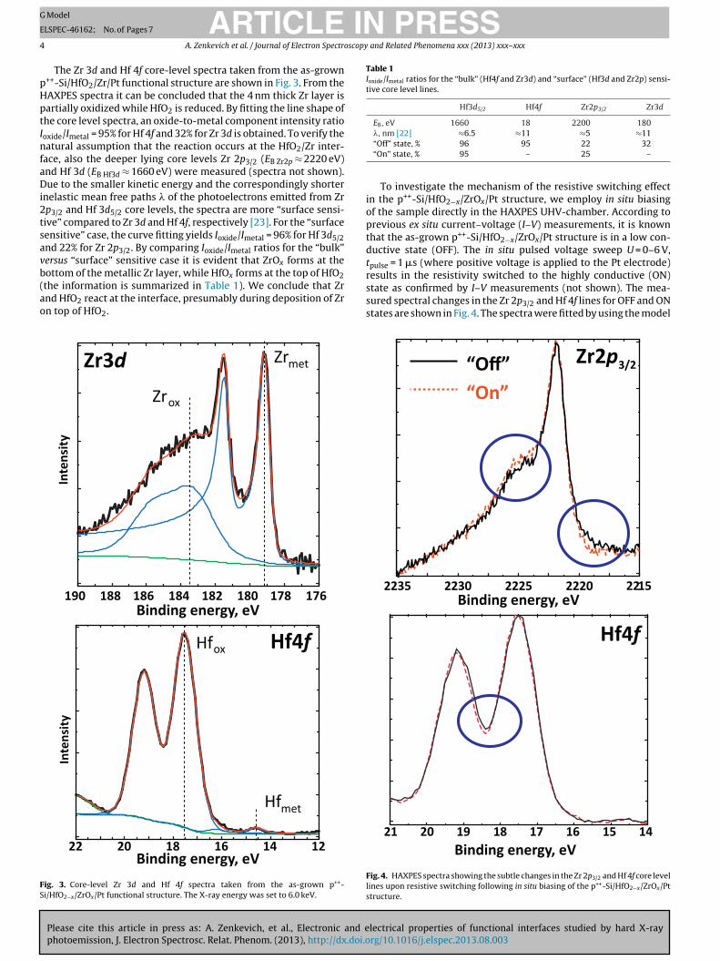
The Zr 3d and Hf 4f core-level spectra taken from the as-grown++-Si/HfO2/Zr/Pt functional structure are shown in Fig. 3. From theAXPES spectra it can be concluded that the 4 nm thick Zr layer isartially oxidized while HfO2 is reduced. By fitting the line shape ofhe core level spectra, an oxide-to-metal component intensity ratiooxide/Imetal = 95% for Hf 4f and 32% for Zr 3d is obtained. To verify theatural assumption that the reaction occurs at the HfO2/Zr inter-
ace, also the deeper lying core levels Zr 2p3/2 (EB Zr2p ≈ 2220 eV)nd Hf 3d (EB Hf3d ≈ 1660 eV) were measured (spectra not shown).ue to the smaller kinetic energy and the correspondingly shorter
nelastic mean free paths � of the photoelectrons emitted from Zrp3/2 and Hf 3d5/2 core levels, the spectra are more “surface sensi-ive” compared to Zr 3d and Hf 4f, respectively [23]. For the “surfaceensitive” case, the curve fitting yields Ioxide/Imetal = 96% for Hf 3d5/2nd 22% for Zr 2p3/2. By comparing Ioxide/Imetal ratios for the “bulk”ersus “surface” sensitive case it is evident that ZrOx forms at the
Please cite this article in press as: A. Zenkevich, et al., Electronic and ephotoemission, J. Electron Spectrosc. Relat. Phenom. (2013), http://dx.doi.o
ottom of the metallic Zr layer, while HfOx forms at the top of HfO2the information is summarized in Table 1). We conclude that Zrnd HfO2 react at the interface, presumably during deposition of Zrn top of HfO2.
190 186 182 178
Zrmet
Zrox
Zr3 d
188 184 180 176
Inte
nsity
22 18 14
Hfmet
Hfox Hf4 f
20 16 12
Inte
nsity
Binding energy, eV
Binding energy, eVig. 3. Core-level Zr 3d and Hf 4f spectra taken from the as-grown p++-i/HfO2−x/ZrOx/Pt functional structure. The X-ray energy was set to 6.0 keV.
�, nm [22] ≈6.5 ≈11 ≈5 ≈11“Off” state, % 96 95 22 32“On” state, % 95 – 25 –
To investigate the mechanism of the resistive switching effectin the p++-Si/HfO2−x/ZrOx/Pt structure, we employ in situ biasingof the sample directly in the HAXPES UHV-chamber. According toprevious ex situ current–voltage (I–V) measurements, it is knownthat the as-grown p++-Si/HfO2−x/ZrOx/Pt structure is in a low con-ductive state (OFF). The in situ pulsed voltage sweep U = 0–6 V,tpulse = 1 �s (where positive voltage is applied to the Pt electrode)
lectrical properties of functional interfaces studied by hard X-rayrg/10.1016/j.elspec.2013.08.003
results in the resistivity switched to the highly conductive (ON)state as confirmed by I–V measurements (not shown). The mea-sured spectral changes in the Zr 2p3/2 and Hf 4f lines for OFF and ONstates are shown in Fig. 4. The spectra were fitted by using the model
Zr2 p3/2
2235 2230 2225 2220 2215
21 20 19 18 17 16 15 14Binding energy, eV
Hf4f
Binding energy, eV
“Off”“On”
Fig. 4. HAXPES spectra showing the subtle changes in the Zr 2p3/2 and Hf 4f core levellines upon resistive switching following in situ biasing of the p++-Si/HfO2−x/ZrOx/Ptstructure.

ARTICLE IN PRESSG Model
ELSPEC-46162; No. of Pages 7
A. Zenkevich et al. / Journal of Electron Spectroscopy and Related Phenomena xxx (2013) xxx– xxx 5
p++ Si
HfO2
ZrOx
Zr
Pt
HfOx
p++ Si
HfO2
ZrOx
Zr
Pt
HfOx
Off state (high resistance)
On state(low resistance)
Fr
ab
t9cresldZoeocTos
tstoWap(d
3
wht4Udt
Pt BaTiO3
φ=1
.36
eV
71.0
4eV
455.
71 e
VE g
= 4.
3eV
EF
Pt4f7/2
Ti2p3/2
387.
61 e
V
2.94
eV
VBM
CBM
ig. 5. Schematic of the chemical evolution of the p++-Si/HfO2−x/ZrOx/Pt stack uponesistive switching as obtained from the HAXPES analysis following in situ biasing.
scribing their evolution to the changes of the Ioxide/Imetal ratio foroth lines.
In particular, for the Zr 2p3/2 line Ioxide/Imetal increases from 22%o 25%, while for Hf 4f the Ioxide/Imetal ratio decreases slightly from6% to 95%. Although these changes are rather small they are indi-ating that the switching from OFF to ON corresponds to a thicknesseduction of HfOx and simultaneous increasing of the ZrOx lay-rs at the interface. This evolution of the interface chemistry ischematically illustrated in Fig. 5. According to this model, the HfO2ayer adjacent to the interface with Zr is rich in oxygen vacanciesue to the initial partial oxidation (reduction) of Zr (HfO2) to formrOx (HfO2−x). During in situ positive biasing the positively chargedxygen vacancies are driven away from HfO2 at the interfaceffectively enriching it with oxygen and thus facilitating furtherxidation of Zr. The latter process produces more oxygen vacan-ies in HfO2 and dramatically increases the conductivity (ON state).he biasing of the opposite sign results in the reversed sequencef reduction/oxidation steps as confirmed by HAXPES (spectra nothown).
The observed effects at the HfO2−x/ZrOx interface supporthe model of an oxidation/reduction mechanism of the resistivewitching in these bilayers. However, the fact that the changes par-icularly in the HfO2 layer are quite small implies that the switchingccurs due to a localized rather than extended area phenomenon.e believe that the generation of the (charged) oxygen vacancies
t the HfO2−x/ZrOx interface and their further drift following theositive (negative) biasing of the stack results in the formation“dissolution”) of the localized conductive paths (filaments) whichefine the resistance switching across the stack.
.2. Conduction band offset in Pt/BaTiO3
Following the HAXPES methodology described above,e determined the valence band offset at the Pt/BaTiO3eteroepitaxial interface by measuring the line separa-ions (EPt4f7/2–EF)Pt = 71.04 ± 0.05 eV, (ETi2p3/2–VBM)BTO =
Please cite this article in press as: A. Zenkevich, et al., Electronic and ephotoemission, J. Electron Spectrosc. Relat. Phenom. (2013), http://dx.doi.o
55.71 ± 0.05 eV and (EPt4f7/2–ETi2p3/2)BTO/Pt = 387.61 ± 0.05 eV.sing formula (1), we then get VBOPt/BTO = 2.94 ± 0.05 eV (moreetailed information is published elsewhere [22]). To determinehe electric potential step height ϕPt/BTO (also known as conduction
Fig. 6. Electronic band diagram at the Pt/BaTiO3 interface as determined by in situHAXPES in combination with ex situ REELS techniques.
band offset, CBO), the band gap Eg for the investigated ultrathinheteroepitaxial BaTiO3 films were determined by ex situ reflectionelectron energy loss spectroscopy (REELS) [21] to be Eg = 4.3 eV.Therefore, the conduction band offset at the Pt/BaTiO3 interfaceis ϕPt/BTO = 1.36 ± 0.05 eV. The band line-up obtained using thesevalues is shown in Fig. 6. We note that according to recent data onthe ferroelectric properties of heteroepitaxial BaTiO3 layers grownon a Pt underlayer, they are spontaneously polarized downward[22], and therefore the potential step is measured for the BaTiO3layer polarization oriented toward Pt. Since the BaTiO3 layer ispolarized, one would expect a potential distribution across thefilm thickness and subsequently a broadening of the spectral linestaken from the constituents of the ferroelectric layer. However,the HAXPES core level data show no line broadening in thefunctional ferroelectrics. According to experimental work [24],surface adsorbates play a governing role in the potential formationmechanism and completely screen the polarization charge on theopen surface of the ferroelectric. Therefore, polarization in thestructurally perfect ferroelectric results in a HAXPES line shiftdue to the formation of electric dipoles at the interface (unlessadsorbates are removed by in situ mild heating in UHV-the effectwill be reported elsewhere).
Another effect which can alter both the line width of HAXPESspectra taken from a ferroelectric and the electronic conditionsat the metal/ferroelectric interface is the presence of fixed and/ormobile charges in the ferroelectric. These charges are particu-larly associated with oxygen vacancies which are the prevailingdefects in complex metal oxide films once they are put in con-tact with metal electrodes [25]. To investigate the possible effectof oxygen vacancies present in BaTiO3 on the band line-up in con-tact with Pt, heteroepitaxial BaTiO3 layers were grown in vacuum(PO2 = 10−7 mbar) and further post-annealed under oxygen with
lectrical properties of functional interfaces studied by hard X-rayrg/10.1016/j.elspec.2013.08.003
different pressures. The changes of the measured Pt/BaTiO3 valenceband offset and the Ba 4d and Ti 2p core level line width as a func-tion of O2 pressure during annealing are shown in Fig. 7a and b,respectively.

ARTICLE ING Model
ELSPEC-46162; No. of Pages 7
6 A. Zenkevich et al. / Journal of Electron Spectroscopy
b)
10-8
10-7
10-6
10-5
10-4
10-3
10-2
10-1
100
10-8
10-7
10-6
10-5
10-4
10-3
10-2
10-1
100
2.65
2.70
2.75
2.80
2.85
2.90
2.95
3.00
3.05
3.10
3.15
VB
O, eV
Oxygen pressure, mbar
а)
Oxygen pressure, mbar
FW
HM
of lin
e, eV
1.15
1.20
1.25
1.30
1.40
1.35
1.45
1.50
1.55
1.60
1.65
1.70
1.75
1.80
1.10
1.05
Ti2p3/2
Ba4d5/2
Fig. 7. BaTiO3 valence band offset with respect to Pt (a) and half-width of Ti2paM
Ptoiwl
Fb
3/2
nd Ba4d5/2 lines (b) as a function of O2 pressure during the post-annealing of thegO/Pt/BaTiO3 heterostructures (T = 500◦ C, t = 30 min) as measured by HAXPES.
The derived evolution of the electronic structure of thet/BaTiO3 interface corroborates the model describing the forma-ion of the electric dipole at the metal/dielectric interface in terms
Please cite this article in press as: A. Zenkevich, et al., Electronic and ephotoemission, J. Electron Spectrosc. Relat. Phenom. (2013), http://dx.doi.o
f electron transfer across the interface from oxygen vacancies (VO)n the ferroelectric – acting as donors – to the metal, once the metal
ork function is sufficiently large [26]. Assuming that the energyevels of (both neutral and charged) oxygen vacancies in BaTiO3
(ESr2s - ETi2p)BTO/LSMO
(ES
Ti2p3
Ti2p3/2Sr2s
Sr2s
458 454462466221522202225 2210
Binding
LSMO reference
BTO reference
BTO/LSMO
ig. 8. HAXPES spectra taken from a LSMO(1 0 0)/BTO(0 0 1) bi-layer as well as from referand offset in the LSMO/BTO heterostructure.
PRESS and Related Phenomena xxx (2013) xxx– xxx
lie in the upper part of the band gap, the high VO concentration inas-grown BaTiO3 results in a decrease of the “effective” work func-tion of Pt in contact giving rise to the larger VBO. The concentrationof VO in BaTiO3 presumably decreases monotonously dependingon the oxygen pressure during the post-annealing, and the VBOsubsequently increases.
Up to 0.3 eV change was predicted in the Pt/SrTiO3 Schottkybarrier height depending on the number of VO [25], while similarcalculations reveal up to 1 eV for the Pt/PZT system as a functionof VO concentration [27]. In this experiment, the observed changeof VBOPt/BTO of ∼0.3 eV depending on the oxygen pressure duringannealing is well within this range. Previously, a similar effect onthe band line-up at the Fe/BaTiO3 interface was observed depend-ing on the top BaTiO3 layer growth conditions [18].
The observed Ba 4d and Ti 2p core level line broadening in BaTiO3following the increase of the oxygen pressure during the annealingis explained by the removal of the mobile (charged) oxygen vacan-cies which contribute to the screening of the electric field insidethe ferroelectric layer.
3.3. Conduction band offset in LSMO/BaTiO3
The analogous HAXPES methodology was adopted to recon-struct the band line-up at the LSMO/BaTiO3 interface, where theconductive LSMO layer is treated as a metal. The line separations(ESr2s–EF)LSMO = 2215.67 eV, (ETi2p3/2–VBM)BTO = 455.71 ± 0.05 eVand (ESr2s–ETi2p3/2)LSMO/BTO = 1756.67 eV were measured for thesingle LSMO layer and BaTiO3 layers on a SrTiO3 substrate, andLSMO/BaTiO3 bi-layers, respectively (Fig. 8). The fact that the shapeof Ti 2p line taken from the BaTiO3 layer exactly coincides withthat from the BaTiO3 reference sample evidences the absence ofspace charge in the bulk of BaTiO3 layer. Using formula (1) adaptedto the LSMO/BaTiO3 system, we calculate the valence band offsetVBOLSMO/BTO = 3.29 ± 0.05 eV, and assuming again the band gap inultrathin BTO layers Eg = 4.3 eV, we get CBOLSMO/BTO = 1.01 ± 0.05 eV(Fig. 9). The obtained value of the conduction band offset at theLSMO/BaTiO3 interface is considerably smaller compared to that atthe Pt/BaTiO3 interface (CBOPt/BaTiO3
= 1.36 eV). These results areconsistent considering much larger vacuum work function valuesof the noble metals such as Pt (WFPt = 5.1 eV) as compared to thatof the (conducting) oxides which may be as low as ∼4 eV. Even
lectrical properties of functional interfaces studied by hard X-rayrg/10.1016/j.elspec.2013.08.003
taking into account the “pinning” effect described above whichoften occurs at the metal oxide/Pt interface, the effective workfunction of Pt in contact with BaTiO3 appears to be larger than thatof LSMO.
Au4f7/284.0 eV
(ETi2p - VBM)BTO
(ETi2p - EF)BTO/LSMO
r2s - EF)LSMO
/2VBM
EF
04812848892
energy, eV
ence LSMO and a BTO thin film grown on a STO substrate to determine the valence

ARTICLE ING Model
ELSPEC-46162; No. of Pages 7
A. Zenkevich et al. / Journal of Electron Spectroscopy
La0.67Sr0.33MnO3 BaTiO3
φ=1
.01
eV
2215
.67
eV
455.
71 e
VE g
= 4.
3eVEF
Sr2sTi2p3/2
1756
.67 e
V
3.29
eV
VBM
CBM
Fm
4
aiocpseaotdbtdoier
A
Pi
[
[
[
[[
[
[[
[
[
[[
[
[
ig. 9. Electronic band diagram at the LaSr0.67Sr0.33O3/BaTiO3 interface as deter-ined by in situ HAXPES in combination with ex situ REELS techniques.
. Conclusion
The HAXPES technique has been successfully employed to char-cterize the chemical and electronic properties of buried interfacesn functional multilayered structures. Using the developed method-logy, we were able to monitor in situ the changes in both thehemical and electronic structure at the metal/insulator interface of++-Si/HfO2−x/ZrOx/Pt stacks accompanying the reversible resistivewitching effect. The electronic band alignment and particularly thelectric potential barrier height were experimentally determinedt the Pt/BaTiO3 and LSMO/BaTiO3 interfaces. An additional resultbtained for Pt/BaTiO3 is that oxygen vacancies present in the ultra-hin BaTiO3 layer affect the interfacial electronic properties. It is stillemanding to directly correlate the spectral information providedy HAXPES with the electronic and electrical (transport) proper-ies of the functional structures modeling the operation of the realevices. The particular challenge, however, is to quantify changesf the electronic conditions at the metal/FE interfaces upon polar-zation reversal in ferroelectric tunnel junctions, or to monitor thevolution of the chemical and/or electronic structure during theesistive switching in metal-insulator-metal trilayers.
cknowledgements
Please cite this article in press as: A. Zenkevich, et al., Electronic and ephotoemission, J. Electron Spectrosc. Relat. Phenom. (2013), http://dx.doi.o
The expert support of the staff at DORIS III beamline BW2 andETRA III beamline P09 is gratefully acknowledged. The HAXPESnstrument at beamline P09 is jointly operated by the University
[[[[
PRESS and Related Phenomena xxx (2013) xxx– xxx 7
of Würzburg (R. Claessen), the University of Mainz (C. Felser)and DESY. We would like to thank Ksenia Maksimova (E. KantBaltic Federal University, Russia) for the assistance in the growthof Pt/BaTiO3/MgO(0 0 1) and BTO/LSMO/STO(0 0 1) heteroepitaxialsamples. This work was financially supported by the Russian Min-istry of Education and Science (Contract No. 11.519.11.3007) andthe German Federal Ministry of Education and Research(BMBF)under contracts 05KS7UM1, 05K10UMA, 05KS7WW3, 05K10WW1and 05K10CHB.
References
[1] Special issue on “Materials for Electronics”, Science 327 (2010).[2] K. Kobayashi, NIMA 601 (2009), 32.[3] T. Nagata, M. Haemori, Y. Yamashita, H. Yoshikawa, Y. Iwashita, K. Kobayashi,
T. Chikyow, APL 97 (2010), 082903.[4] T. Nagata, M. Haemori, Y. Yamashita, H. Yoshikawa, Y. Iwashita, K. Kobayashi,
T. Chikyow, APL 99 (2011), 223517.[5] R. Claessen, M. Sing, M. Paul, G. Berner, A. Wetscherek, A. Müller, W. Drube,
New J. Phys. 11 (2009), 125007.[6] R. Waiser, R. Dittmann, G. Staikov, K. Szot, Adv. Mater. 21 (2009) 2632.[7] J. Lee, E.M. Bourim, W. Lee, J. Park, M. Jo, S. Jung, J. Shin, H. Hwang, APL 97 (2010)
172105.[8] P. Calka, E. Martinez, D. Lafond, S. Minoret, S. Tirano, B. Detlefs, J. Roy, J. Zegen-
hagen, C. Guedj, J. Appl. Phys. 109 (2011) 124506.[9] M.Ye. Zhuravlev, R.F. Sabirianov, S.S. Jaswal, E.Y. Tsymbal, Phys. Rev. Lett. 94
(2005) 246802.10] A. Gruverman, D. Wu, H. Lu, Y. Wang, H.W. Jang, C.M. Folkman, M.Ye. Zhuravlev,
D. Felker, M. Rzchowski, C.-B. Eom, E.Y. Tsymbal, Nano Lett. 9 (2009) 3539.11] A. Chanthbouala, A. Crassous, V. Garcia, K. Bouzehouane, S. Fusil, X. Moya, J.
Allibe, B. Dlubak, J. Grollier, S. Xavier, et al., Nat. Nanotechnol. 7 (2012) 101.12] K.J. Choi, M. Biegalski, Y.L. Li, A. Sharan, J. Schubert, R. Uecker, P. Reiche, Y.B.
Chen, X.Q. Pan, V. Gopalan, L.-Q. Chen, D.G. Schlom, C.B. Eom, Science 306 (2004)1005.
13] C.-G. Duan, S.S. Jaswal, E.Y. Tsymbal, Phys. Rev. Lett. 97 (2006) 047201.14] V. Garcia, M. Bibes, L. Bocher, S. Valencia, F. Kronast, A. Crassous, X. Moya, S.
Enouz-Vedrenne, A. Gloter, D. Imhoff, et al., Science 327 (2010) 1106.15] A. Gloskovskii, G. Stryganyuk, G.H. Fecher, C. Felser, S. Thiess, H. Schulz-Ritter,
W. Drube, G. Berner, M. Sing, R. Claessen, M. Yamamoto, J. El. Spec. Rel. Phenom.185 (2012) 47.
16] http://unifit-software.de.17] E.A. Kraut, R.W. Grant, J.R. Waldrop, S.P. Kowalczyk, Phys. Rev. Lett. 44 (1980)
1620.18] A. Zenkevich, R. Mantovan, M. Fanciulli, M. Minnekaev, Yu.A. Matveyev, Yu.Yu.
Lebedinskii, S. Thiess, W. Drube, Appl. Phys. Lett. 99 (2011) 182905.19] Yu. Matveyev, A. Zenkevich, Yu. Lebedinskii, S. Thiess, W. Drube, Microelectr.
Eng. 88 (2011) 1353.20] A. Zenkevitch, I. Khabelashvili, J. Chevallier, Thin Solid Films 311 (1997) 119.21] A. Zenkevich, M. Minnekaev, Yu. Lebedinskii, K. Bulakh, A. Chouprik, A. Baturin,
R. Mantovan, M. Fanciulli, O. Uvarov, Thin Solid Films 520 (2012) 4586.22] A. Zenkevich, Minnekaev M., Yu. A. Matveyev, Yu. Lebedinskii, K. Bulakh, A.
Chouprik, K. Maksimova, A. Baturin, S. Thiess, W. Drube, Appl. Phys. Lett. 102(2013) 062907.
23] In this work we adopt � values for the specified core level photoelectrons inHfO2 (ZrO2) the same as those previously measured for SiO2 layer for similarkinetic energies [18] (see Table 1), and the sampling depths are thus estimated
lectrical properties of functional interfaces studied by hard X-rayrg/10.1016/j.elspec.2013.08.003
∼10 nm and ∼22 nm for the “bulk” and “surface sensitive” cases, respectively.24] S.V. Kalinin, D.A. Bonnell, Phys. Rev. B 63 (2001) 125411.25] J. Robertson, O. Sharia, A. Demkov, App. Phys. Lett. 91 (2007) 132912.26] M. Dawber, K.M. Rabe, J.F. Scott, Rev. Mod. Phys. 77 (2005) 1083.27] M. Dawber, J.F. Scott, Int. Ferroelectr. 38 (2001), 161.