Impedance analysis of Bi3.25La0.75Ti3O12 ferroelectric ceramic
12
PRAMANA c Indian Academy of Sciences Vol. 71, No. 3 — journal of September 2008 physics pp. 599–610 Impedance analysis of Bi 3.25 La 0.75 Ti 3 O 12 ferroelectric ceramic S RACHNA 1 , SURYA M GUPTA 1 and S BHATTACHARYYA 2,* 1 Laser Materials Development and Devices Division, Raja Ramanna Centre for Advanced Technology, Indore 452 013, India 2 Department of Metallurgical and Materials Engineering, Colorado School of Mines, Golden, USA * Corresponding author. E-mail: sudipto [email protected] MS received 26 September 2006; revised 20 November 2007; accepted 4 March 2008 Abstract. AC impedance spectroscopy technique has been used to study electrical prop- erties of Bi 3.25 La 0.75 Ti 3 O 12 (BLT) ceramic. Complex impedance plots were fitted with three depressed semicircles, which are attributed to crystalline layer, plate boundary and grain boundary and all three were found to comprise of universal capacitance nature [C = C0w n-1 ]. Grain boundary resistance and capacitance evaluated from complex im- pedance plots have larger values than that of plate boundary and crystalline layer. The activation energies (E a ) for DC-conductance in grain boundary, plate boundary and crys- talline layer are 0.68 eV, 0.89 eV and 0.89 eV, respectively. Relaxation activation energies calculated from impedance plots showed similar values, 0.81 eV and 0.80 eV for crystalline layer and plate boundary, respectively. These activation energy values are found to be consistent with the E a value of oxygen vacancies in perovskite materials. A mechanism is offered to explain the generation of oxygen vacancies in BLT ceramic and its role in temperature dependence of DC-conductance study. Keywords. Ferroelectric memories; impedance; Bi-layered structure; oxygen ion-jump. PACS Nos 84.37.+q; 77.84.-S; 85.50.Gk; 82.45.Xy; 77.84.Lf 1. Introduction La-doped bismuth titanate (BLT) is a promising material for ferroelectric random access memory (FRAM), because of its low processing temperature and polarization retention up to 10 10 switch cycles on Pt-electrodes [1,2]. Bismuth titanate (BT) is a layered structure ferroelectric, which belongs to the Aurivillius family of compounds [3]. The general formula of BT can be written as (Bi 2 O 2 ) 2+ (A m-1 B m O 3m+1 ) 2- , where A is Bi 3+ , B is Ti 4+ and m = 3 [4–6]. Thus, the stoichiometric composition is Bi 4 Ti 3 O 12 . The unit cell consists of alter- nating layers of (Bi 2 O 2 ) 2+ and three pseudo-perovskite layers of oxygen octahedra of (Bi 2 Ti 3 O 10 ) 2- stacked in the c-direction [7,8]. The polarization direction is in 599
-
Upload
independent -
Category
Documents
-
view
4 -
download
0
Transcript of Impedance analysis of Bi3.25La0.75Ti3O12 ferroelectric ceramic

PRAMANA c© Indian Academy of Sciences Vol. 71, No. 3— journal of September 2008
physics pp. 599–610
Impedance analysis of Bi3.25La0.75Ti3O12
ferroelectric ceramic
S RACHNA1, SURYA M GUPTA1 and S BHATTACHARYYA2,∗1Laser Materials Development and Devices Division, Raja Ramanna Centre for AdvancedTechnology, Indore 452 013, India2Department of Metallurgical and Materials Engineering, Colorado School of Mines,Golden, USA∗Corresponding author. E-mail: sudipto [email protected]
MS received 26 September 2006; revised 20 November 2007; accepted 4 March 2008
Abstract. AC impedance spectroscopy technique has been used to study electrical prop-erties of Bi3.25La0.75Ti3O12 (BLT) ceramic. Complex impedance plots were fitted withthree depressed semicircles, which are attributed to crystalline layer, plate boundary andgrain boundary and all three were found to comprise of universal capacitance nature[C = C0w
n−1]. Grain boundary resistance and capacitance evaluated from complex im-pedance plots have larger values than that of plate boundary and crystalline layer. Theactivation energies (Ea) for DC-conductance in grain boundary, plate boundary and crys-talline layer are 0.68 eV, 0.89 eV and 0.89 eV, respectively. Relaxation activation energiescalculated from impedance plots showed similar values, 0.81 eV and 0.80 eV for crystallinelayer and plate boundary, respectively. These activation energy values are found to beconsistent with the Ea value of oxygen vacancies in perovskite materials. A mechanismis offered to explain the generation of oxygen vacancies in BLT ceramic and its role intemperature dependence of DC-conductance study.
Keywords. Ferroelectric memories; impedance; Bi-layered structure; oxygen ion-jump.
PACS Nos 84.37.+q; 77.84.-S; 85.50.Gk; 82.45.Xy; 77.84.Lf
1. Introduction
La-doped bismuth titanate (BLT) is a promising material for ferroelectric randomaccess memory (FRAM), because of its low processing temperature and polarizationretention up to 1010 switch cycles on Pt-electrodes [1,2].
Bismuth titanate (BT) is a layered structure ferroelectric, which belongs to theAurivillius family of compounds [3]. The general formula of BT can be writtenas (Bi2O2)2+(Am−1BmO3m+1)2−, where A is Bi3+, B is Ti4+ and m = 3 [4–6].Thus, the stoichiometric composition is Bi4Ti3O12. The unit cell consists of alter-nating layers of (Bi2O2)2+ and three pseudo-perovskite layers of oxygen octahedraof (Bi2Ti3O10)2− stacked in the c-direction [7,8]. The polarization direction is in
599

S Rachna, Surya M Gupta and S Bhattacharyya
the ab-plane at 4.5◦ to a-axis [9–11]. The plate-like grain morphology gives riseto electrical anisotropy with the higher component of its spontaneous polarization(PS = 50 µC/cm2) parallel to the bismuth layers [12–14].
Recently, impedance spectroscopy of BLT ceramics has been reported [15] inwhich the complex impedance spectra above 250◦C were fitted by assuming anequivalent circuit comprising of the contributions of grain and grain boundaries.The experimental data were shown to fit remarkably up to 360◦C. Above the tran-sition temperature (>400◦C), the fitted low frequency data were found to deviatefrom the experimental data. It has already been reported [12] that a single crystalof BT consists of mica-like aspects when observed under scanning electron mi-croscope. The impedance spectroscopy revealed two depressed semicircles. Thedepressed semicircle at low frequency was assigned to the plate boundary and thesecond depressed semicircle at high frequency was corresponding to bulk. The plateboundaries were present in the crystal and thus three semicircles are expected inthe AC-impedance results of BLT ceramics. In view of this we have carried outimpedance studies on BLT, with the aim to investigate the true picture of the elec-trical properties and its correlation with the sample microstructure. The results arefitted with a series addition of three depressed semicircles corresponding to grainand two barriers (i) plate and (ii) grain boundary.
2. Experimental details
Bi3.25La0.75Ti3O12 ceramic was prepared using the conventional solid-state reactionroute. Stoichiometric amounts of high purity starting reagents Bi2O3, La2O3 andTiO2 were mixed thoroughly with acetone and then ball-milled for 18 h. The slurrywas dried at 80◦C and the powder was calcined at 800◦C for 4 h. Single phaseformation of BLT pseudo-orthorhombic phase was confirmed by X-ray diffraction(XRD). The calcined powder was ball-milled again with acetone for 12 h. Afterdrying, the powder was pressed into cylinders using polyvinyl alcohol (PVA) as abinder and a uniaxial hydrostatic pressure of 120 MPa. These cylinders were firedat 1100◦C for 2 h after binder burnout at 450◦C for 4 h. These cylinders were firedunder covered alumina crucible, and a small amount of Bi2O3 powder was placednear the sample in order to minimize bismuth oxide loss. All sintered pellets had afinal density greater than 98% of the theoretical value. The calcined and sinteredspecimens were analysed by Rigaku X-ray diffractometer, operated at 30 KV and20 mA, using CuKα radiation for second phase formation. The sintered blockswere then cut into thin disks and polished on different grades of emery papers toobtain parallel surfaces. The polished surfaces were ultrasonically cleaned to removedust particles. Sample discs using a thin coating of high temperature drying silverpaste (cured at 500◦C for two hours in air) were used as electrodes to ensure goodelectrical contact.
The dielectric response was measured using a Hewlett-Packard 4194A impedanceanalyzer which can cover a frequency range of 100 to 15 × 106 Hz. For high tem-perature measurements, the samples were placed in a custom-built tube furnace,which can be operated between 30 and 800◦C. The temperature was measured us-ing a Eurotherm controller 800 via a K-type thermocouple mounted directly on the
600 Pramana – J. Phys., Vol. 71, No. 3, September 2008

Impedance analysis of Bi3.25La0.75Ti3O12
Figure 1. X-ray diffraction pattern of sintered Bi3.25La0.75Ti3O12 ceramicat room temperature.
insulation (alumina) of the ground electrode of the sample fixture. The impedanceanalyzer and Eurotherm controller were interfaced with computer to collect datawhile cooling as well as heating at a rate of 2◦C/min.
Impedance measurement was carried out using HP 4194A impedance analyzerover a frequency range of 100 Hz to 1 MHz, at different temperatures (up to 500◦C).The temperature was held constant for 10–15 min to obtain equilibrium. Impedanceresults were analysed using commercially available Z-View software [16].
3. Results and discussion
3.1 Phase and microstructural studies
Figure 1 shows X-ray diffraction pattern of Bi3.25La0.75Ti3O12 ceramic. All the ma-jor diffraction peaks were indexed with pure Bi4Ti3O12 orthorhombic phase. Nopeak corresponding to pyrochlore and fluorite type was detected. Lattice parame-ters a = 5.42 A, b = 5.41 A, c = 32.89 A and α, β, γ = 90◦ were determined.
Scanning electron micrograph of the fractured surface of the sintered specimen isshown in figure 2. Well-developed plate-like grains with average grain size of ∼5 µmin length and ∼2 µm in width could be seen. Similar plate-like grain morphologyhas already been reported for BLT sintered ceramic [17]. The sintered density wasmeasured using the Archimedes principle and 98% of the theoretical density wasmeasured.
Pramana – J. Phys., Vol. 71, No. 3, September 2008 601

S Rachna, Surya M Gupta and S Bhattacharyya
Figure 2. Scanning electron micrograph of the fractured surface of the sin-tered BLT ceramic.
3.2 Impedance and dielectric analysis
Figure 3a shows the temperature dependence of real dielectric constant at differentfrequencies. The Curie temperature Tc was obtained from the peak value of thetemperature dependence of dielectric constant plot. Tc was estimated to be 400◦Cat 1 MHz frequency and that is consistent with the reported value [18]. Strongfrequency dispersion was observed for BLT ceramic with increasing temperature.High conducting losses masks the peak corresponding to phase transition at allfrequency (<100 kHz) in temperature dependence of dielectric constant plot. Figure3b shows the variation of dissipation factor with temperature at various frequencies.A low frequency tan δ peak was observed between 150◦C and 300◦C temperaturerange. According to Debye model, reciprocal frequency of each peak gives relaxationtime τ (in sec). When relaxation time versus reciprocal of peak temperature isplotted, a straight line is observed (inset of figure 3b). The plot is fitted with theArrhenius relationship, where slope is equal to the activation energy (Ea), as shownin eq. (1):
τ = τ0 exp(−Ea/kBT ), (1)
where τ0 is the time constant, k is the Boltzmann’s constant and T is the temper-ature at which the relaxation peak is maximum.
Relaxation activation energy 0.87 eV with time constant τ0 = 7.86e−12 s wascalculated. These parameters are indicative of ion-jump or dipole relaxation [19,20].An oxygen ion hopping has been proposed to attribute the relaxation observed inthis temperature regime [21].
Figures 4a,b show the variation of real and imaginary impedance (Z ′ and Z ′′)with frequency at different temperatures. The Z ′ value was found to decrease withincreasing frequency at all temperatures. The Z ′ also decreased with increasing
602 Pramana – J. Phys., Vol. 71, No. 3, September 2008
Impedance analysis of Bi3.25La0.75Ti3O12
Figure 3. Dependence of (a) ε′ and (b) tan δ on temperature for frequenciesranging from 100 Hz to 1 MHz. (Inset of figure 3b shows variation of relaxationtime with inverse of temperature.)
temperature, which is due to an increase in the conducting losses. The frequencycorresponding to Z ′′max shifted to higher values with increasing temperature. Thepeak height for both the peaks (figure 4b) was decreased with increase of temper-ature indicating an increase in the conducting loss.
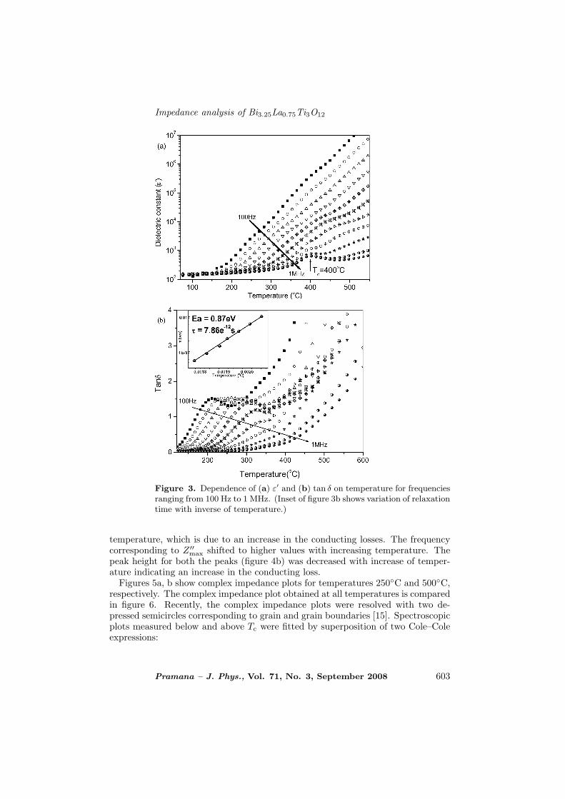
Figures 5a, b show complex impedance plots for temperatures 250◦C and 500◦C,respectively. The complex impedance plot obtained at all temperatures is comparedin figure 6. Recently, the complex impedance plots were resolved with two de-pressed semicircles corresponding to grain and grain boundaries [15]. Spectroscopicplots measured below and above Tc were fitted by superposition of two Cole–Coleexpressions:
Pramana – J. Phys., Vol. 71, No. 3, September 2008 603
S Rachna, Surya M Gupta and S Bhattacharyya
Figure 4. Spectroscopic (a) real and (b) imaginary part of impedance (Z′)plots of BLT in the temperature range 325◦C–475◦C. Solid lines are fittingresults with the proposed equivalent circuit presented in figure 5a.
Z∗ = R1/1 + (iωτ1)m + R2/1 + (iωτ2)n, (2)
where R1, R2, τ1 and τ2 are resistances and relaxation times for grain and grainboundaries, respectively. The above equation was reported to fit well with thespectroscopic plots of BLT below Tc but strong deviation could be seen in lowfrequency regime above Tc. The proposed equivalent circuit [15] was also used tofit our experimental data. The inset of figure 5b shows the fitting of experimentaldata at 500◦C with eq. (2). It should be noticed that the experimental data of lowfrequency does not match properly, as marked by arrows. These experimental plotswere fitted by equivalent circuit model as shown in figure 5a. The experimental plotswere completely resolved into three depressed semicircles, i.e. semicircle centred
604 Pramana – J. Phys., Vol. 71, No. 3, September 2008

Impedance analysis of Bi3.25La0.75Ti3O12
Figure 5. Experimental, simulated, theoretical and deconvoluted compleximpedance plots of BLT at (a) 250◦C and (b) 500◦C. Series addition of 3RQ-type equivalent circuit used for fitting experimental data is shown. Inset offigure 5b shows fitting of experimental data at 500◦C assuming 2RQ.
below the abscissa axis, suggests the relaxation to be of non-Debye type. Thesolid line in figures 4a, b and 6 is the fitting of the experimental data by theequivalent circuit as shown in figure 5a. Excellent fitting of experimental data withthe proposed equivalent circuit may be noticed.
Considering complex impedance plots of BT single crystal and ceramic as re-ported by Huanosta et al [17] and Macedo et al [22], respectively, low, intermedi-ate and high frequency arcs were ascribed to grain boundary, plate boundary andcrystalline layer, respectively. Each depressed semicircle is represented by parallelresistance-constant phase element (RQ) circuit. The constant phase element (CPE)is expressed by eq. (3) and defined by two values, C0 and n [23–25],
C = C0(jω)n−1, (3)
Pramana – J. Phys., Vol. 71, No. 3, September 2008 605

S Rachna, Surya M Gupta and S Bhattacharyya
Figure 6. Nyquist diagram of the sintered BLT ceramic above and below(inset) the transition temperature. The temperature is marked in the respec-tive plot. Fitting results using 3RCPE-type equivalent circuit is shown bysolid line.
where C0 is expressed in units of capacitance component and ω is the angularfrequency (=2πf). The CPE is identical to a capacitance component when theexponent n = 1, to a resistance component when n = 0, and to a Warburg compo-nent when n = 0.5. When CPE is placed parallel to a resistance, a Cole element(depressed semicircle) is produced.
The value of circuit parameters were estimated by nonlinear least square fittingwith the aid of the program Z-view [15]. The capacitances (CCL, CPB, and CGB)and exponent n (nCL, nPB and nGB) due to crystalline layer, plate boundary andgrain boundaries were obtained by fitting Nyquist plots at all temperatures. Figure7 shows the temperature variation of CCL, CPB, CGB, nCL, nPB and nGB obtainedfrom the Nyquist plots. A sudden change in capacitance of CCL, CPB, and CGB isattributed to ferroelectric transition at Tc. The capacitance of the crystalline layerwas found to decrease above the transition temperature, which is consistent withthe ferroelectric nature of the grain of BLT. An increase in CPB and CGB aboveTc may be due to the defect contribution in this temperature regime. From thetemperature variation of n, nGB was found to decrease with increase of tempera-ture below and above Tc, which depicts a clear departure from the ideal behaviour.Abnormal change in the value of nCL, nPB and nGB at Tc may be attributed toincrease of disorder at Tc. Similarly, an abnormal change in the fitting parameters(coefficient A and exponent S from the power relation proposed by Jonscher) nearthe Curie temperature for ferromagnetic spinel (Zn0.44Mn0.56Fe2O4) and ferroelec-tric perovskite (Sr0.25Bi4Ti3.25O12.75) were attributed to an increase in the disordernear the phase transition [26].
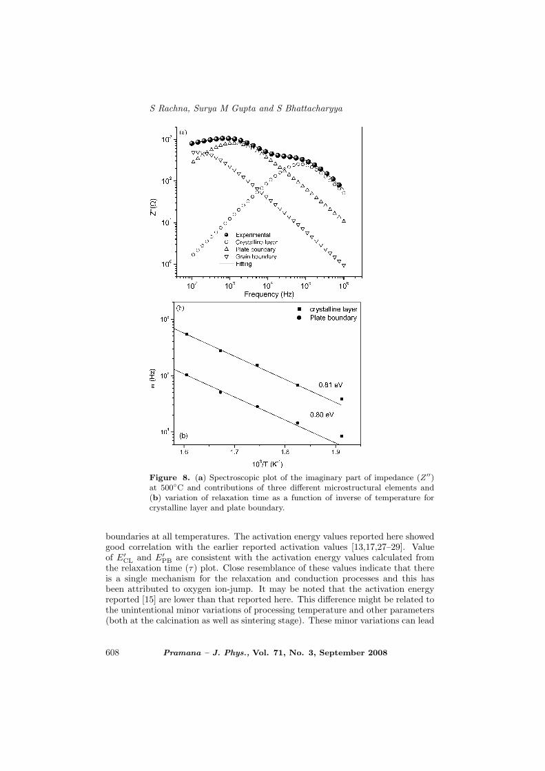
Figure 8a shows the de-convoluted spectroscopic plots of three microstructuralelements as well as the fitting curve along with the experimental data points. Therelaxation time was calculated for each microstructural element at all temperatures
606 Pramana – J. Phys., Vol. 71, No. 3, September 2008

Impedance analysis of Bi3.25La0.75Ti3O12
Figure 7. Comparison of temperature-dependent exponent n and capaci-tance C0 for the crystalline layer, plate boundary and grain boundaries.
below Tc. At the peak, the relaxation time τm is defined by eq. (4):
ωmτm = 1, (4)
where ωm is the relaxation frequency. Figure 8b shows that the relaxation timeobey the Arrhenius relation given by eq. (1). The activation energy, Ea, calculatedfrom the plot of log τm vs. 1/T , is 0.81 eV and 0.80 eV for crystalline layer andplate boundary, respectively. A close resemblance of two values indicates that plateboundary and crystalline layer has the same type of relaxation processes. Theactivation energy values are in good agreement with the ion-jump mechanism [21].The convoluted peak corresponding to the grain boundaries was quite broad, andso relaxation time for grain boundary could not be calculated.
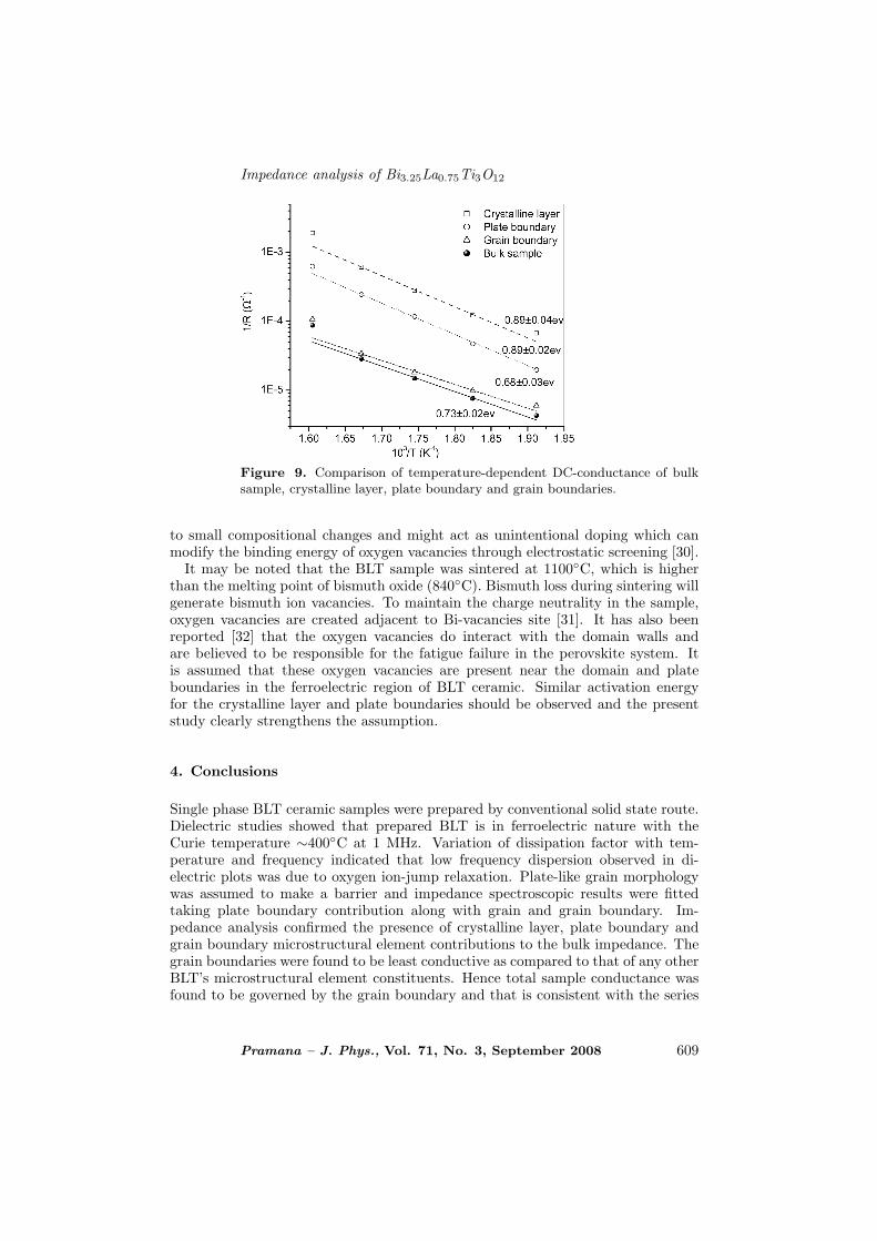
The radius of deconvoluted arc in complex impedance is equal to electrical re-sistance of the microstructural region. The resistance of crystalline layer (RCL),plate boundary (RPL) and grain boundary (RGB) were obtained at all tempera-tures from the fitting of the Nyquist plots. DC-resistance of bulk sample (Rbulk)was obtained from series addition of the DC-resistance of the individual microstruc-tural elements. Figure 9 shows the temperature variation of inverse of RCL, RPB,RGB, and Rbulk below Tc. It can be seen that grain boundaries are more resis-tive than plate boundary and crystalline layer in the observed temperature range.Hence bulk resistance (Rbulk) is governed by grain boundaries. From figure 9, theactivation energy for the DC-conductance of all three microstructural elements wascalculated. The nature of conductance at various temperatures was almost linearand obeyed the Arrhenius relationship
σDC = σ0 exp(−E′a/kBT ), (5)
where E′a is the activation energy of conduction and T is the absolute temperature.
The values E′CL = 0.89 ± 0.04 eV, E′
PB = 0.89 ± 0.02 eV, E′GB = 0.68 ± 0.03 eV
and E′bulk = 0.73± 0.02 eV were calculated in the ferroelectric region. The activa-
tion energy for grain boundaries was lower than that of crystalline plate or plate
Pramana – J. Phys., Vol. 71, No. 3, September 2008 607
S Rachna, Surya M Gupta and S Bhattacharyya
Figure 8. (a) Spectroscopic plot of the imaginary part of impedance (Z′′)at 500◦C and contributions of three different microstructural elements and(b) variation of relaxation time as a function of inverse of temperature forcrystalline layer and plate boundary.
boundaries at all temperatures. The activation energy values reported here showedgood correlation with the earlier reported activation values [13,17,27–29]. Valueof E′
CL and E′PB are consistent with the activation energy values calculated from
the relaxation time (τ) plot. Close resemblance of these values indicate that thereis a single mechanism for the relaxation and conduction processes and this hasbeen attributed to oxygen ion-jump. It may be noted that the activation energyreported [15] are lower than that reported here. This difference might be related tothe unintentional minor variations of processing temperature and other parameters(both at the calcination as well as sintering stage). These minor variations can lead
608 Pramana – J. Phys., Vol. 71, No. 3, September 2008
Impedance analysis of Bi3.25La0.75Ti3O12
Figure 9. Comparison of temperature-dependent DC-conductance of bulksample, crystalline layer, plate boundary and grain boundaries.
to small compositional changes and might act as unintentional doping which canmodify the binding energy of oxygen vacancies through electrostatic screening [30].
It may be noted that the BLT sample was sintered at 1100◦C, which is higherthan the melting point of bismuth oxide (840◦C). Bismuth loss during sintering willgenerate bismuth ion vacancies. To maintain the charge neutrality in the sample,oxygen vacancies are created adjacent to Bi-vacancies site [31]. It has also beenreported [32] that the oxygen vacancies do interact with the domain walls andare believed to be responsible for the fatigue failure in the perovskite system. Itis assumed that these oxygen vacancies are present near the domain and plateboundaries in the ferroelectric region of BLT ceramic. Similar activation energyfor the crystalline layer and plate boundaries should be observed and the presentstudy clearly strengthens the assumption.
4. Conclusions
Single phase BLT ceramic samples were prepared by conventional solid state route.Dielectric studies showed that prepared BLT is in ferroelectric nature with theCurie temperature ∼400◦C at 1 MHz. Variation of dissipation factor with tem-perature and frequency indicated that low frequency dispersion observed in di-electric plots was due to oxygen ion-jump relaxation. Plate-like grain morphologywas assumed to make a barrier and impedance spectroscopic results were fittedtaking plate boundary contribution along with grain and grain boundary. Im-pedance analysis confirmed the presence of crystalline layer, plate boundary andgrain boundary microstructural element contributions to the bulk impedance. Thegrain boundaries were found to be least conductive as compared to that of any otherBLT’s microstructural element constituents. Hence total sample conductance wasfound to be governed by the grain boundary and that is consistent with the series
Pramana – J. Phys., Vol. 71, No. 3, September 2008 609

S Rachna, Surya M Gupta and S Bhattacharyya
addition of resistances. Oxygen ion-jump process is believed to be responsible forthe DC-conduction and dielectric relaxation present in the crystalline layer andplate boundary.
References
[1] B H Park, B S Kang, S Bu, T W Noh, J Lee and W Jo, Nature (London) 401, 682(1999)
[2] E Rokuta, J H Choi, Y Hotta, H Tabata, H Kobayashi and T Kawai, Appl. Phys.Lett. 79, 1858 (2001)
[3] B Aurivillius, Ark Kemi 1, 499 (1949)[4] J F Scott and C A Pazde Arajuo, Science 246, 1400 (1989)[5] C A Paz de Araujo, J D Cuchiaro, L D McMillan, M C Scott and J F Scott, Nature
(London) 374, 627 (1995)[6] S B Desu and D P Vijay, Mater. Sci. Engg. B32, 75 (1995)[7] E C Subbarao, J. Phys. Chem. Solids 23, 665 (1962)[8] C Javalekic and S Stevic, Ferroelectrics 132, 185 (1992)[9] S E Cummins and L E Cross, J. Appl. Phys. 39, 2268 (1968)
[10] P C Joshi and S B Krupanidhi, Appl. Phys. Lett. 62, 1928 (1993)[11] T Kijima, M Ushikubo and M Matsunaga, Jpn. J. Appl. Phys. 38, 127 (1999)[12] A Fouskova and L E Cross, J. Appl. Phys. 41, 2834 (1970)[13] S Eharta, K Muramatsu, M Shimazu, J Tanaka, M Tsukioka, Y Mori, T Hattori and
H Tamura, Jpn. J. Appl. Phys. 20, 877 (1981)[14] Masatake Takahashi, Yuji Noguchi and Masaru Miyayama, Jpn. J. Appl. Phys. 41,
7053 (2002)[15] J H Park, J S Bae, B C Choi and J H Jeong, J. Phys. D40, 579 (2007)[16] D Johnson, Software Zview-v 2.3d, Scribner Associates Inc. (2000)[17] A Huanosta, O Alvarez-Fregoso and E Amano, J. Appl. Phys. 69, 404 (1991)[18] T Takenaka and K Sakata, Ferroelectrics 38, 769 (1981)[19] W D Kingery, H K Bowen and D R Uhlmann, Introduction to ceramics (Wiley, New
York, 1976)[20] K H Hardtl, Ceram. Int. 8(4), 121 (1982)[21] Holly S Shulman, J. Am. Ceram. Soc. 80(3), 528 (2000)[22] Z S Macedo, C R Ferrari and A C Hernandes, J. European Ceramic Soc. 24, 2567
(2004)[23] J R MacDonald, Impedance spectroscopy – emphasizing solid materials and systems
(John Wiley & Sons, 1987)[24] A K Jonscher, Dielectric relaxation in solids (Chelsea, London, 1983)[25] X S Gao, J M Xue and J Wang, J. Appl. Phys. 97, 034101 (2005)[26] A Pelaiz-Barranco, M P Gutierrez-Amador, A Huanosta and R Valenzuela, Appl.
Phys. Lett. 73(14), 2039 (1998)[27] O A Fregoso, J. Appl. Phys. 81, 1387 (1997)[28] W Li, D Su, J Zhu and Y Wang, Solid State Commun. 131, 189 (2004)[29] S K Kim, M Miyayama and H Yanagida, Mater. Res. Bull. 31, 121 (1996)[30] A D Brailsford and D K Honke, Solid State Ionics 11, 235 (1983)[31] S Rachna, Sudipto Bhattacharyya and S M Gupta, J. Phys. Chem. Solids 69, 822
(2008)[32] H N Al-Shareef, D Dimos, T J Boyle, W L Warren and B A Tuttle, Appl. Phys. Lett.
68, 690 (1996)
610 Pramana – J. Phys., Vol. 71, No. 3, September 2008