
Photonic Components for Analog Fiber Links
38
Chapter 7 © 2012 García Juárez et al., licensee InTech. This is an open access chapter distributed under the terms of the Creative Commons Attribution License (http://creativecommons.org/licenses/by/3.0), which permits unrestricted use, distribution, and reproduction in any medium, provided the original work is properly cited. Photonic Components for Analog Fiber Links Alejandro García Juárez, Ignacio Enrique Zaldívar Huerta, Jorge Rodríguez Asomoza and María del Rocío Gómez Colín Additional information is available at the end of the chapter http://dx.doi.org/10.5772/48416 1. Introduction Currently, several companies are involved in the transport of radiofrequency (RF) or microwave signals radio over fiber links (RoF). RoF links are considered a promising technique in providing broadband wireless access services in the emerging optical-wireless networks. The modulation scheme which decides the way to generate the optical millimeter- wave signal is a key technique in this optical-wireless access network architecture [1–3]. The simplest RoF system consists of a Central Site (CS) and a Remote Site (RS) connected by an optical fiber link or network. The frequencies of the radio signals distributed by RoF systems span a wide range (usually in the GHz region) and the applications for such systems range from in-building distribution of wireless signals (for example in shopping malls and tunnels), wireline interconnections between base stations and microcellular antennas, antenna remoting for various commercial (wing-tip antennas in aircraft) and military radar systems and broadcasting of cable television signals in both hybrid fiber coax (HFC) and triplexer based fiber-to-the-home (FTTH) systems [4]. On the other hand a traditional RF photonic link operating at 1550 nm consists of a directly modulated DFB laser diode, a length of fiber optic as transmission medium, and a photo-detector (PD) [5]. The fiber chromatic dispersion intrinsically occurring in standard 1550 nm single-mode fibers (SMFs) is one of the main drawbacks that limit the transmission distance and operation bandwidth of such RF fiber-optic systems. However if low dispersion fiber is used in conjunction with an appropriate choice of the laser operating parameters the system becomes quasi linear [6]. DFB lasers are the proper light sources for these applications because of their single longitudinal mode, with side-mode suppression ratio (SMSR) in the order of 40 dB, and stable operation with a narrow spectral width. However, the characteristic relaxation oscillations peak in the laser intensity which produce sidebands on both sides of the main laser line, impose a limiting factor on the proximity of two channels in a communication system. Besides these characteristics, limit the high frequency response of semiconductor lasers and the sensitivity in low frequency applications. In order for an optical analog
-
Upload
independent -
Category
Documents
-
view
1 -
download
0
Transcript of Photonic Components for Analog Fiber Links
Chapter 7
© 2012 García Juárez et al., licensee InTech. This is an open access chapter distributed under the terms of the Creative Commons Attribution License (http://creativecommons.org/licenses/by/3.0), which permits unrestricted use, distribution, and reproduction in any medium, provided the original work is properly cited.
Photonic Components for Analog Fiber Links
Alejandro García Juárez, Ignacio Enrique Zaldívar Huerta, Jorge Rodríguez Asomoza and María del Rocío Gómez Colín
Additional information is available at the end of the chapter
http://dx.doi.org/10.5772/48416
1. Introduction
Currently, several companies are involved in the transport of radiofrequency (RF) or
microwave signals radio over fiber links (RoF). RoF links are considered a promising
technique in providing broadband wireless access services in the emerging optical-wireless
networks. The modulation scheme which decides the way to generate the optical millimeter-
wave signal is a key technique in this optical-wireless access network architecture [1–3]. The
simplest RoF system consists of a Central Site (CS) and a Remote Site (RS) connected by an
optical fiber link or network. The frequencies of the radio signals distributed by RoF systems
span a wide range (usually in the GHz region) and the applications for such systems range
from in-building distribution of wireless signals (for example in shopping malls and
tunnels), wireline interconnections between base stations and microcellular antennas,
antenna remoting for various commercial (wing-tip antennas in aircraft) and military radar
systems and broadcasting of cable television signals in both hybrid fiber coax (HFC) and
triplexer based fiber-to-the-home (FTTH) systems [4]. On the other hand a traditional RF
photonic link operating at 1550 nm consists of a directly modulated DFB laser diode, a
length of fiber optic as transmission medium, and a photo-detector (PD) [5]. The fiber
chromatic dispersion intrinsically occurring in standard 1550 nm single-mode fibers (SMFs)
is one of the main drawbacks that limit the transmission distance and operation bandwidth
of such RF fiber-optic systems. However if low dispersion fiber is used in conjunction with
an appropriate choice of the laser operating parameters the system becomes quasi linear [6].
DFB lasers are the proper light sources for these applications because of their single
longitudinal mode, with side-mode suppression ratio (SMSR) in the order of 40 dB, and
stable operation with a narrow spectral width. However, the characteristic relaxation
oscillations peak in the laser intensity which produce sidebands on both sides of the main
laser line, impose a limiting factor on the proximity of two channels in a communication
system. Besides these characteristics, limit the high frequency response of semiconductor
lasers and the sensitivity in low frequency applications. In order for an optical analog
Optical Communication 130
transmission of GHz-range signal to be successful in RoF systems, it is necessary to have a
good DFB laser without their inherently serious problem of the modulation distortion
caused by several factors: spatial-hole burning (SHB), leakage current, nonlinear interaction
of carriers and photons, gain compression, nonlinear I-V characteristics in a p-n
heterojunction, and power dependent absorption and including relaxation oscillations
frequencies. However, recently the authors have demonstrated in reference [7] that when a
DFB laser biased in the low laser threshold current region, relaxation oscillation frequencies
in the laser intensity appear. These frequencies were seen as sidebands on both sides of the
main laser line when the optical spectrum was analyzed with a spectrum analyzer. This
result allowed the generation of microwave signals on C band using direct detection
method. In addition with the proposed experimental setup in [7], the authors also
demonstrate an analog NTSC TV signal transmitted and satisfactorily received in a short
distance wireline communication system by using relaxation oscillation frequency as an
information carrier. The proposed microwave photonic link architecture used to transmit
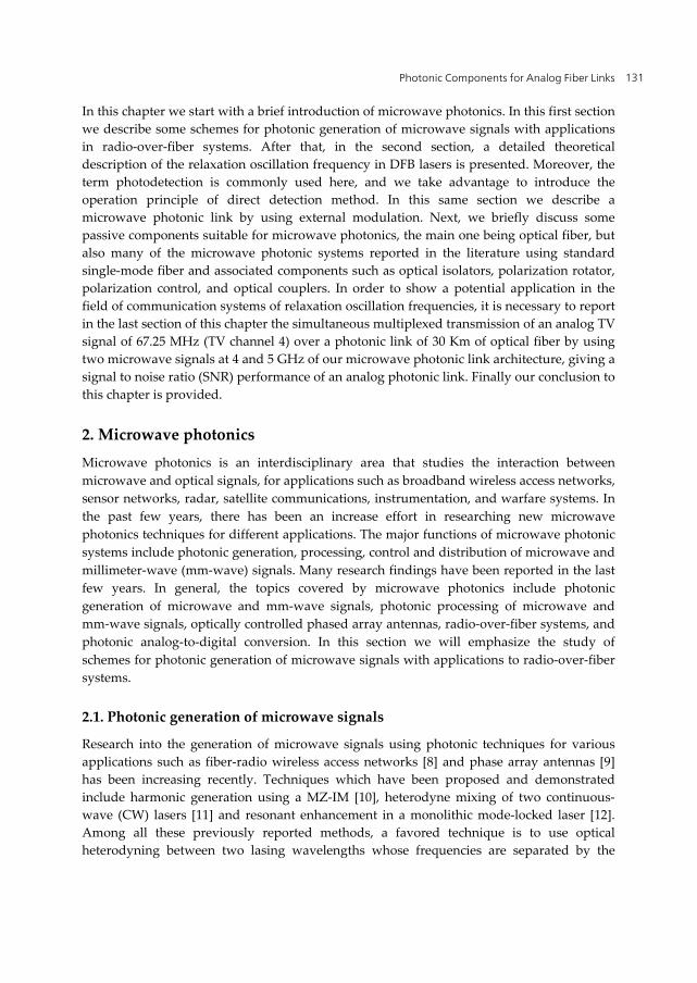
simultaneously a TV signal at 4 and 5 GHz and over 30 km of standard optical fiber is
shown in Figure 1.
Figure 1. Experimental setup for transmitting a TV signal by using relaxation oscillation frequency as
information carrier.
The procedure proposed here starts with the use of two DFB laser diodes emitting at
1550 nm and operating in the low laser threshold current region. When the generated
emissions in both lasers are detected by a fast photo-detector using direct detection method,
two relaxation oscillation frequencies are obtained. These frequencies acting as information
carriers are mixed with TV signals. The signal obtained in the output of the mixer is printed
on an optical carrier as an intensity modulation using a MZ-IM. The intensity-modulated
optical carrier is then transmitted over 30 km of optical fiber. At the end of the link, a
photodiode is used to convert the intensity modulation back to the relaxation oscillation
frequencies mixed with TV signals. After that, TV signals are recovered satisfactorily.
Photonic Components for Analog Fiber Links 131
In this chapter we start with a brief introduction of microwave photonics. In this first section
we describe some schemes for photonic generation of microwave signals with applications
in radio-over-fiber systems. After that, in the second section, a detailed theoretical
description of the relaxation oscillation frequency in DFB lasers is presented. Moreover, the
term photodetection is commonly used here, and we take advantage to introduce the
operation principle of direct detection method. In this same section we describe a
microwave photonic link by using external modulation. Next, we briefly discuss some
passive components suitable for microwave photonics, the main one being optical fiber, but
also many of the microwave photonic systems reported in the literature using standard
single-mode fiber and associated components such as optical isolators, polarization rotator,
polarization control, and optical couplers. In order to show a potential application in the
field of communication systems of relaxation oscillation frequencies, it is necessary to report
in the last section of this chapter the simultaneous multiplexed transmission of an analog TV
signal of 67.25 MHz (TV channel 4) over a photonic link of 30 Km of optical fiber by using
two microwave signals at 4 and 5 GHz of our microwave photonic link architecture, giving a
signal to noise ratio (SNR) performance of an analog photonic link. Finally our conclusion to
this chapter is provided.
2. Microwave photonics
Microwave photonics is an interdisciplinary area that studies the interaction between
microwave and optical signals, for applications such as broadband wireless access networks,
sensor networks, radar, satellite communications, instrumentation, and warfare systems. In
the past few years, there has been an increase effort in researching new microwave
photonics techniques for different applications. The major functions of microwave photonic
systems include photonic generation, processing, control and distribution of microwave and
millimeter-wave (mm-wave) signals. Many research findings have been reported in the last
few years. In general, the topics covered by microwave photonics include photonic
generation of microwave and mm-wave signals, photonic processing of microwave and
mm-wave signals, optically controlled phased array antennas, radio-over-fiber systems, and
photonic analog-to-digital conversion. In this section we will emphasize the study of
schemes for photonic generation of microwave signals with applications to radio-over-fiber
systems.
2.1. Photonic generation of microwave signals
Research into the generation of microwave signals using photonic techniques for various
applications such as fiber-radio wireless access networks [8] and phase array antennas [9]
has been increasing recently. Techniques which have been proposed and demonstrated
include harmonic generation using a MZ-IM [10], heterodyne mixing of two continuous-
wave (CW) lasers [11] and resonant enhancement in a monolithic mode-locked laser [12].
Among all these previously reported methods, a favored technique is to use optical
heterodyning between two lasing wavelengths whose frequencies are separated by the
Optical Communication 132
desired microwave frequency. Optical heterodyning also has the advantage over other
generation techniques of generating high RF power, though optical sources with narrow
linewidth or feedback loops are required during operation [13]. The following section
includes descriptions of the most common techniques to generate microwave signals using
the optical heterodyning method, including optical injection locking (OIL) of laser diodes
[14], external modulation technique [15], dual-mode semiconductor laser sources [16] as
well as using the optical phase locked loop (OPLL) configuration [17].
2.1.1. Optical heterodyning
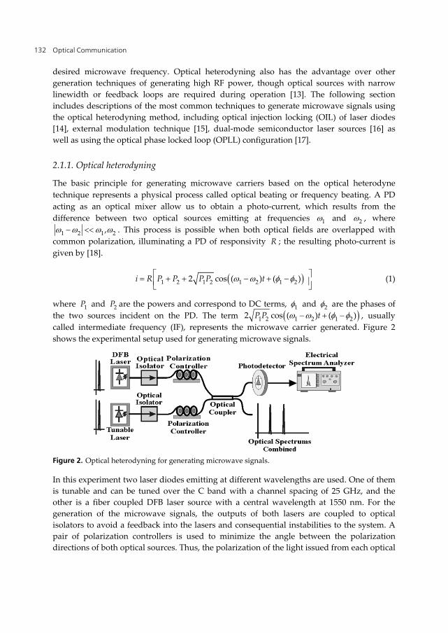
The basic principle for generating microwave carriers based on the optical heterodyne
technique represents a physical process called optical beating or frequency beating. A PD
acting as an optical mixer allow us to obtain a photo-current, which results from the
difference between two optical sources emitting at frequencies 1 and 2 , where
1 2 1 2, . This process is possible when both optical fields are overlapped with
common polarization, illuminating a PD of responsivity R ; the resulting photo-current is
given by [18].
1 2 1 2 1 2 1 22 cos ( ) ( )i R P P P P t (1)
where 1P and 2P are the powers and correspond to DC terms, 1 and 2 are the phases of
the two sources incident on the PD. The term 1 2 1 2 1 22 cos ( ) ( )P P t , usually
called intermediate frequency (IF), represents the microwave carrier generated. Figure 2
shows the experimental setup used for generating microwave signals.
Figure 2. Optical heterodyning for generating microwave signals.
In this experiment two laser diodes emitting at different wavelengths are used. One of them
is tunable and can be tuned over the C band with a channel spacing of 25 GHz, and the
other is a fiber coupled DFB laser source with a central wavelength at 1550 nm. For the
generation of the microwave signals, the outputs of both lasers are coupled to optical
isolators to avoid a feedback into the lasers and consequential instabilities to the system. A
pair of polarization controllers is used to minimize the angle between the polarization
directions of both optical sources. Thus, the polarization of the light issued from each optical
Photonic Components for Analog Fiber Links 133
source is matched and therefore, there is no degradation of the power levels in the
microwave signals generated in the PD. The output of each controller is launched to a 3 dB
coupler to combine both optical spectrums. After that, an optical output signal is received by
a fast PD. The resulting photo-current from the PD corresponds to the microwave beat
signal which is analyzed with an Electrical Spectrum Analyzer (ESA). The other optical
output resulting from an optical coupler is applied to an Optical Spectrum Analyzer (OSA)
for monitoring the wavelength of the two beams. DFB laser sources provide the ability to
control not only the output optical power of the fiber coupled laser diode, but also the
precise the temperature at which the laser is operating. Both controls can be used to tune the
fiber coupled laser diode to an optimum operating point, providing a stable output. In this
way, we can observe that the wavelength of the DFB laser is shifting by varying its
temperature with a scale of 1ºC. Consequently, the beat signal frequency is continuously
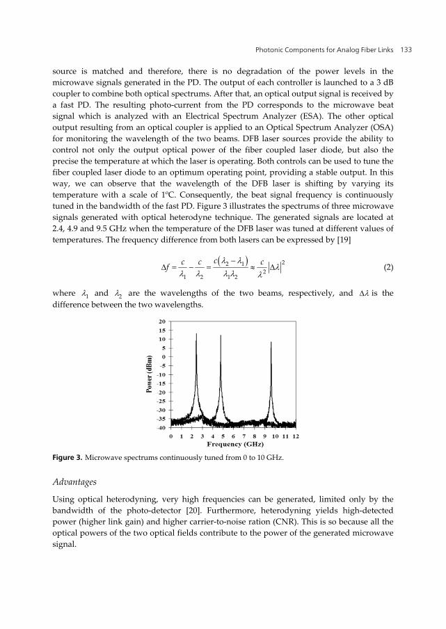
tuned in the bandwidth of the fast PD. Figure 3 illustrates the spectrums of three microwave
signals generated with optical heterodyne technique. The generated signals are located at
2.4, 4.9 and 9.5 GHz when the temperature of the DFB laser was tuned at different values of
temperatures. The frequency difference from both lasers can be expressed by [19]
22 1
21 2 1 2
cc c cf
(2)
where 1 and 2 are the wavelengths of the two beams, respectively, and is the
difference between the two wavelengths.
Figure 3. Microwave spectrums continuously tuned from 0 to 10 GHz.
Advantages
Using optical heterodyning, very high frequencies can be generated, limited only by the
bandwidth of the photo-detector [20]. Furthermore, heterodyning yields high-detected
power (higher link gain) and higher carrier-to-noise ration (CNR). This is so because all the
optical powers of the two optical fields contribute to the power of the generated microwave
signal.
Optical Communication 134
Disadvantages
Beating two optical waves from two free-running laser diodes would lead to a microwave or
mm-wave signal with high phase noise since the phases of the two optical waves are not
correlated. They would also be transferred to the generated microwave or mm-wave signal as
shown in Eq. (1). Therefore, the generated RF signal is very sensitive to phase noise. Since
semiconductor lasers are prone to phase noise, extra measures to minimize the noise have to be
taken. Techniques used to reduce phase noise sensitivity, OIL and OPLL, are discussed below.
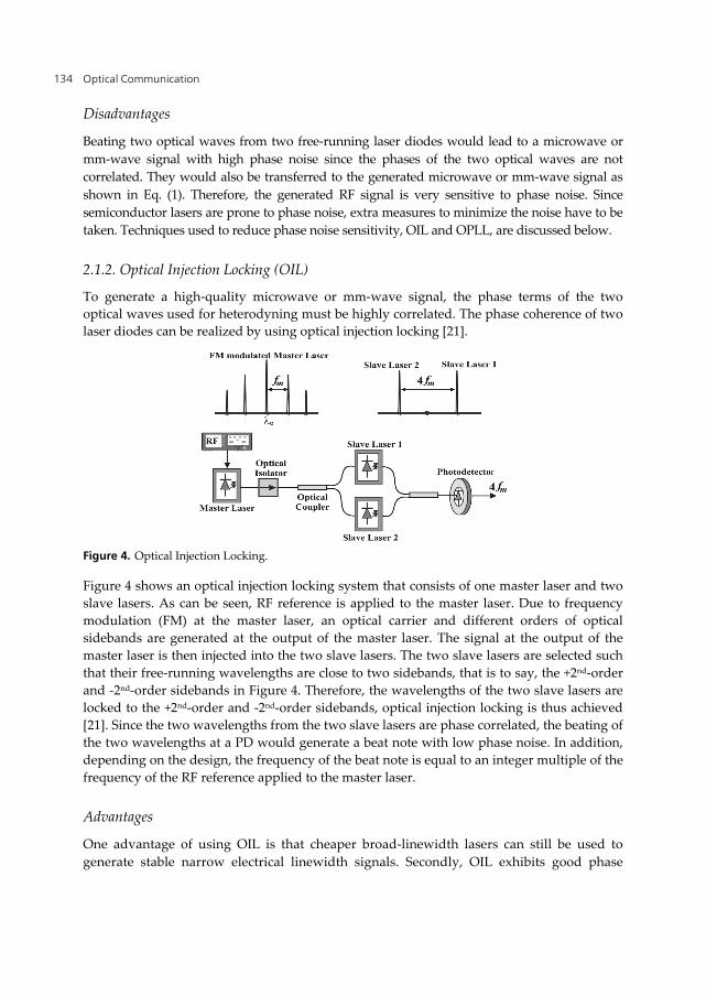
2.1.2. Optical Injection Locking (OIL)
To generate a high-quality microwave or mm-wave signal, the phase terms of the two
optical waves used for heterodyning must be highly correlated. The phase coherence of two
laser diodes can be realized by using optical injection locking [21].
Figure 4. Optical Injection Locking.
Figure 4 shows an optical injection locking system that consists of one master laser and two
slave lasers. As can be seen, RF reference is applied to the master laser. Due to frequency
modulation (FM) at the master laser, an optical carrier and different orders of optical
sidebands are generated at the output of the master laser. The signal at the output of the
master laser is then injected into the two slave lasers. The two slave lasers are selected such
that their free-running wavelengths are close to two sidebands, that is to say, the +2nd-order
and -2nd-order sidebands in Figure 4. Therefore, the wavelengths of the two slave lasers are
locked to the +2nd-order and -2nd-order sidebands, optical injection locking is thus achieved
[21]. Since the two wavelengths from the two slave lasers are phase correlated, the beating of
the two wavelengths at a PD would generate a beat note with low phase noise. In addition,
depending on the design, the frequency of the beat note is equal to an integer multiple of the
frequency of the RF reference applied to the master laser.
Advantages
One advantage of using OIL is that cheaper broad-linewidth lasers can still be used to
generate stable narrow electrical linewidth signals. Secondly, OIL exhibits good phase
Photonic Components for Analog Fiber Links 135
noise suppression. Thirdly, because the slave laser locks on to a sub-harmonic of its
resonance frequency, low frequency reference signals are used. OIL is simpler and easier to
achieve.
Disadvantages
The major disadvantage of OIL is that it has a small frequency detuning range. Optimum
phase noise suppression occurs only at one point of slave laser detuning relative to the free-
running frequency.
2.1.3. Optical Phase Locked-Loops (OPLL)
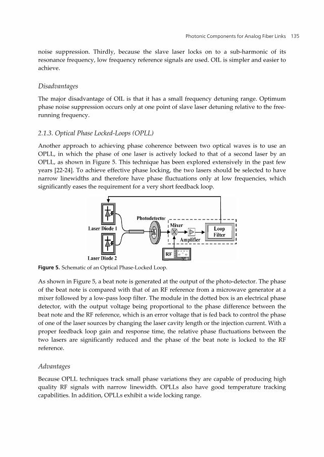
Another approach to achieving phase coherence between two optical waves is to use an
OPLL, in which the phase of one laser is actively locked to that of a second laser by an
OPLL, as shown in Figure 5. This technique has been explored extensively in the past few
years [22-24]. To achieve effective phase locking, the two lasers should be selected to have
narrow linewidths and therefore have phase fluctuations only at low frequencies, which
significantly eases the requirement for a very short feedback loop.
Figure 5. Schematic of an Optical Phase-Locked Loop.
As shown in Figure 5, a beat note is generated at the output of the photo-detector. The phase
of the beat note is compared with that of an RF reference from a microwave generator at a
mixer followed by a low-pass loop filter. The module in the dotted box is an electrical phase
detector, with the output voltage being proportional to the phase difference between the
beat note and the RF reference, which is an error voltage that is fed back to control the phase
of one of the laser sources by changing the laser cavity length or the injection current. With a
proper feedback loop gain and response time, the relative phase fluctuations between the
two lasers are significantly reduced and the phase of the beat note is locked to the RF
reference.
Advantages
Because OPLL techniques track small phase variations they are capable of producing high
quality RF signals with narrow linewidth. OPLLs also have good temperature tracking
capabilities. In addition, OPLLs exhibit a wide locking range.

Optical Communication 136
Disadvantages
The major drawback of OPLLs is that they require far more complex laser structures such as
3-contact DFBs. This requirement is a direct consequence of the fact that to track the
frequency perturbations of the master laser, the tuning rate of the slave laser must be
sufficiently high. This also implies that sufficient feedback bandwidth must be available.
The required feedback bandwidth is determined by the summed laser linewidth, the
requirements for loop stability, and phase noise requirements placed on the optical
microwave signal by the system in which the OPLL is to be applied. A wide feedback
bandwidth is necessary if semiconductor lasers are used, because they have a large amount
of phase noise. In order to achieve the wide feedback bandwidth, the loop-propagation
delay must be small.
2.1.4. Microwave generation based on external modulation
In addition to the techniques using optical injection locking and OPLL, high-quality
microwave signals can also be generated based on external modulation [25–27]. A method to
generate a mm-wave signal using an external optical modulation technique was first
proposed in 1992 [25]. A frequency-doubled electrical signal was optically generated by
biasing the MZ-IM to suppress the even-order optical sidebands ( 2 f method ). A 36 GHz
mm-wave signal was generated when the MZ-IM was driven by an 18 GHz microwave
signal. Such a system was employed for a remote delivery of video services [26]. In 1994,
another method was proposed to generate a frequency-quadrupled electrical signal ( 4 f
method). Instead of biasing the MZ-IM to suppress the even-order optical sidebands, the
method in [10] was based on the quadratic response of an optical intensity modulator. The
optical carrier and the first and third-order optical sidebands were suppressed by adjusting
the drive signal level. A 60 GHz millimeter-wave signal was generated when a 15 GHz drive
signal was applied to the MZ-IM.
Figure 6. Microwave signal generation based on external modulation.
Figure 6 shows a system to generate a continuously tunable mm-wave signal based on
external modulation using a MZ-IM and a wavelength-fixed optical filter [28]. The
significance of the technique is that no tunable optical filter is required, which significantly

Photonic Components for Analog Fiber Links 137
simplifies the system implementation. As can be seen from Figure 6, the system consists of a
MZ-IM that is biased at the maximum transmission point of the transfer function to
suppress the odd-order optical sidebands. A fiber Bragg grating (FBG) serving as a
wavelength-fixed notch filter is then used to filter out the optical carrier. A stable, low-phase
noise mm-wave signal that has four times the frequency of the RF drive signal is generated
at the output of the PD.
Advantages of the 2f and 4f methods
Both the 2f and 4f methods rely on optical heterodyning. Therefore, they are capable of
generating high frequency mm-waves. Since the same laser generates both optical fields, the
phase noise is highly correlated resulting in very narrow linewidth mm-waves. In fact, the
performance of these methods in terms of phase noise is comparable to the OPLL system. A
key advantage of these approaches in [26,27] is that an optical modulator with a maximum
operating frequency of 15 GHz can generate a millimeter-wave signal up to 60 GHz.
Disadvantage of the 2f and 4f methods
The main disadvantage of these techniques is that both approaches use optical filters to
select the two optical sidebands. Another disadvantage is that in order to generate tunable
mm-wave signals, a tunable optical filter must be used. These two disadvantages
significantly increase the complexity and the cost of the system.
2.1.5. Microwave generation using a dual-wavelength laser
Microwave signals can also be generated using a dual wavelength laser source with the two
wavelengths separated at a desired frequency [29]. It is different from the techniques of
optical injection locking and the OPLL because, the two wavelengths from a dual
wavelength laser source are not locked in phase. However, due to the fact that the two
wavelengths are generated inside same cavity, the phase correlation between the two
wavelengths is better than that using two free-running laser sources. To ensure that the two
wavelengths are in single-longitudinal mode, a dual-band filter with ultra-narrow
passbands must be used, thus, limiting the number of longitudinal modes to one in each
passband. In the experimental demonstration [29], the ultra-narrow dual-band filter was a
dual-wavelength ultra-narrow transmission band FBG with two ultra-narrow transmission
bands, which was designed and fabricated based on the equivalent phase-shift (EPS)
technique [30].
Advantages
The advantage of using a dual-wavelength laser source to generate a microwave or mm-
wave signal is that the system is simpler with no need for a microwave reference source,
which can significantly reduce the system cost. Due to the fact that the two wavelengths are
generated from the same cavity, the phase correlation between the two wavelengths is better
Optical Communication 138
than that using two free-running laser sources. The spectral width of the generated
microwave signals is as small as 80 kHz with frequency stability better than 1 MHz in the
free-running mode at room temperature.
Disadvantages
Due to the fact that three dual-wavelength ultranarrow transmission-bands can be
incorporated into the laser cavity by using this technique, then microwave signals
continuously tuned can not be generated.
3. Relaxation oscillation frequency
The relaxation oscillation frequency is the frequency of the quasi-sinusoidal oscillations
around the steady state output power amplitude that occur during the disturbance of a
continuously operating laser. Such oscillations are characterized by exponential damping.
The phenomenon of relaxation oscillations has an effect on the performance of an
unmodulated laser as well, by producing sidebands in the field fluctuation spectrum. They
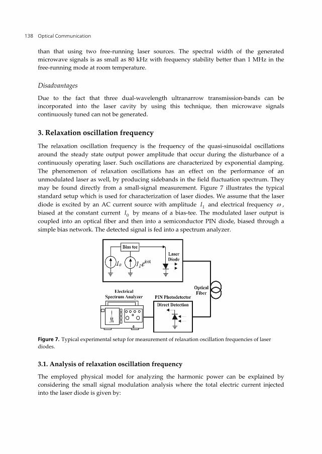
may be found directly from a small-signal measurement. Figure 7 illustrates the typical
standard setup which is used for characterization of laser diodes. We assume that the laser
diode is excited by an AC current source with amplitude 1I and electrical frequency ,
biased at the constant current 0I by means of a bias-tee. The modulated laser output is
coupled into an optical fiber and then into a semiconductor PIN diode, biased through a
simple bias network. The detected signal is fed into a spectrum analyzer.
Figure 7. Typical experimental setup for measurement of relaxation oscillation frequencies of laser
diodes.
3.1. Analysis of relaxation oscillation frequency
The employed physical model for analyzing the harmonic power can be explained by
considering the small signal modulation analysis where the total electric current injected
into the laser diode is given by:
Photonic Components for Analog Fiber Links 139
0 1j tI I I e (3)
If photon and electron densities inside the active region of a semiconductor laser are
denoted, respectively, by PN and EN , then expanding PN and EN as a Fourier series we
find that these densities can be written as:
0
jn tE En
n
N N e
(4)
0
jn tP Pn
n
N N e
(5)
where PnN and EnN are the corresponding expansion coefficients of the photon and
electron densities, respectively. On the other hand, the well-known rate equations for a
single mode laser diode are [31]
E Ei g E tr P
e
dN NIV a N N N
dt qV
(6)
P Pg E tr P
p
dN NV a N N N
dt (7)
here i is the efficiency coefficient; e is the carrier lifetime; a is the differential gain; trN is
the threshold electron density; is the cavity confinement factor; gV is the cavity volume;
and p is the photon lifetime. In order to obtain information related with harmonic contents
in optical output power of a laser diode, it is necessary to start our approach by substituting
Eqs. (3) to (5) in Eq. (6) which results in
0 1
1 0
0 0
1j t
jn t jn tEn i En
n ne
jn t jn tg En tr Pn
n n
I I ej N ne N e
qV
V a N e N N e
(8)
In a similar way, if we substitute Eqs. (4) and (5) in Eq. (7) we obtain
1 0 0
0
1
jn t jn t jn tPn g En tr Pn
n n n
jn tPn
np
j N ne V a N e N N e
N e
(9)
From DC Analysis (n = 0), however, we have:
Optical Communication 140
0
0
0
0
1
i g tr P
E
g Pe
IV aN N
qVN
V aN
(10)
0
1g E tr
p
V a N N
(11)
The first harmonic of the photon density is generated directly by the first harmonic of the
current applied to the laser diode, and we easily obtain [32]
1
0
1
1 11
i
E
g Pe p
I
qVN
j V aNj
(12)
0
1 1
g P
P E
V aNN N
j
(13)
Higher harmonics are found from recursive equations which in the general case for an
arbitrary integer, 1k , may be written as:
0 0
1
1k
kEk
Ek g E tr P Ek P En Pk nne
Njk N V a N N N N N N N
(14)
0
1
1
k
Pk g Ek P En Pk nn
jk N V a N N N N
(15)
Hence, the kth harmonic of the photon density may be calculated once all the lower
harmonics of photon and electron densities are known. If we define kM as the parameter
which relates the kth harmonic to the lower ones [33]
1
1
k
k En Pk nn
M N N
(16)
Therefore, we can find the kth harmonics of photon and electron densities as
0
11
1 11
k
gp
E k
g Pe p
V ajk
N M
jk V aNjk
(17)
Photonic Components for Analog Fiber Links 141
0k k
gP P E k
V aN N N M
jk
(18)
The frequency, RO , at which the amplitude of the power harmonic content reaches its
maximum is called the Relaxation Resonant Frequency. From Eqs. (12) and (13), the primary
harmonic of the photon density is obtained as [32]
0
1
0
1
1 11
ig P
P
g Pe p
IV aN qV
Nj
j V aNj
(19)
On the other hand, if the optical output power for the kth harmonic is given by
p
k outk pkm
hvVP P N
, where m is the mirror loss time, pV represents the cavity volume
and hv is the energy per photon, then by using this last equation we can obtain the optical
output power for the first harmonic, written as
0
0
1
12
( )
1
g P ip
g Pmp
e p
IV aN
hvV qVP j
V aNjj
(20)
The cavity confinement factor, , is equal to the ratio, pV V ; therefore, the above can be
written as:
0
0
1
1 2
1
( )
( )1
g P im
g P
pe p
hvV aNqP j
V aNI j jj
(21)
By separating the real and imaginary parts of the denominator of Eq. (21), we finally
get [33]
0
0
0
1
1 2
1
( )
( ) 1
g P im
g P
g Pp e
hvV aNqP j
V aNI jj V aN
(22)
This expression clearly has two poles at:
Optical Communication 142
0 0 0
12 2
1 1 1 1 1
4 2g P g P g Pp e e
V aN V aN j V aN
(23)
which are located in the first and second quadrants of the complex plane. We now notice
that the real part of the denominator of Eq. (22) becomes zero at the frequency:
02 g P
ROp
V aN
(24)
where 2RO ROf . Since usually 0
1g P RO
p
V aN
holds, we conclude that the
magnitude of Eq. (22) also reaches a maximum when RO . Hence, the denominator
becomes purely imaginary, and the primary power harmonic content reaches its resonance
mode. The optimum modulation frequency is the resonant frequency, which is determined
from the bias current. Therefore, the optimal operation point for modulation where the
power of the primary harmonic reaches its maximum must lie on the curve obtained from
the following [34].
0g
RO i thp
V aI I
qV (25)
From the laser rate equations it is clear that the relaxation oscillation frequency should be
proportional to the square root of the difference of the injection current and the threshold
current. Thus, from Eq. (25) we can see that there is a linear relationship between relaxation
oscillation frequency and the square root of the difference between the injection current and
the threshold current. On the other hand, when the laser current density is lightly increased
above its threshold value, the laser output power may be written as [35].
1.24
( )o d in tho
P I I
(26)
where 1.24
do
is called the differential responsivity of the laser (W/A).
4. Operation principle of direct detection
When a laser is biased in the threshold current region as shown in Figure 8, the laser
intensity presents oscillations know as relaxation frequencies and can be seen as sidebands
on both sides of the main laser line. In this case the electric field emitted by the laser diode
can be represented as a directly modulated optical signal. After passing through an optical
fiber, the optical field incident on the PD can be expressed as [36, 37]
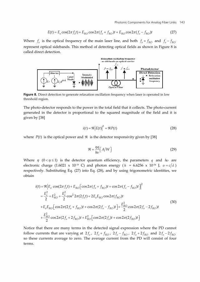
Photonic Components for Analog Fiber Links 143
( ) cos(2 ) cos2 ( ) cos2 ( )o o RO o RO RO o ROE t E f t E f f t E f f t (27)
Where of is the optical frequency of the main laser line, and both o ROf f and o ROf f
represent optical sidebands. This method of detecting optical fields as shown in Figure 8 is
called direct detection.
Figure 8. Direct detection to generate relaxation oscillation frequency when laser is operated in low
threshold region.
The photo-detector responds to the power in the total field that it collects. The photo-current
generated in the detector is proportional to the squared magnitude of the field and it is
given by [38]
2
( ) ( ) ( )i t E t P t (28)
where ( )P t is the optical power and is the detector responsivity given by [38]
q
A Wh
(29)
Where (0 1) is the detector quantum efficiency, the parameters q and h are
electronic charge (1.6021 x 10⁻¹⁹ C) and photon energy ( h = 6.6256 x 10⁻³⁴ J, c )
respectively. Substituting Eq. (27) into Eq. (28), and by using trigonometric identities, we
obtain
2
`
2 22 2
2
22
( ) cos(2 ) cos2 ( ) cos2 ( )
cos 2 (2 ) 2 cos2 ( )2 2
cos2 (2 ) cos2 (2 ) cos2 (2 2 )2
cos 2 (2 2 ) cos2 (22
o o RO o RO o RO
o oRO o o RO RO
ROo RO o RO o RO o RO
ROo RO RO
i t E f t E f f t f f t
E EE f t E E f t
EE E f f t f f t f f t
Ef f t E f
) cos2 (2 )o ROt f t
(30)
Notice that there are many terms in the detected signal expression where the PD cannot
follow currents that are varying at 2 of , 2 o ROf f , 2 o ROf f , 2 2o ROf f and 2 2o ROf f
so these currents average to zero. The average current from the PD will consist of four
terms.
Optical Communication 144
2
2 2( ) 2 cos2 ( ) cos2 (2 )2o
RO o RO RO RO RO
Ei t E E E f t E f t
(31)
The photo-current generated at the PD is found in a similar way as
( ) 2 cos2 ( ) cos2 (2 )2o
RO o RO RO RO RO
Pi t P P P f t P f t
(32)
The first two terms correspond to DC photo-currents and contain no information, but they
do contribute to the shot noise of the signal detected. The next two terms correspond to the
signal information which contains the relaxation oscillation frequency ROf and its harmonic
located at 2 ROf .
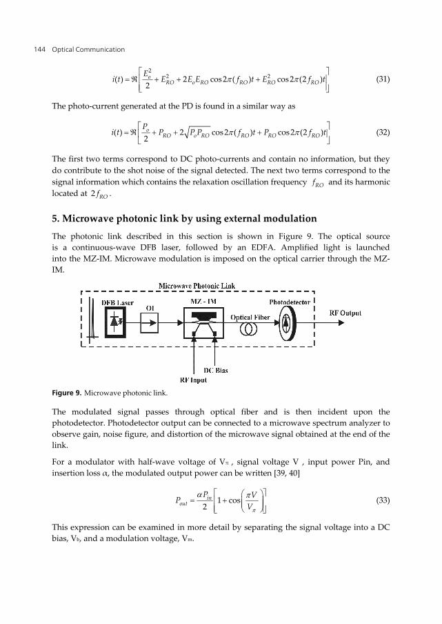
5. Microwave photonic link by using external modulation
The photonic link described in this section is shown in Figure 9. The optical source
is a continuous-wave DFB laser, followed by an EDFA. Amplified light is launched
into the MZ-IM. Microwave modulation is imposed on the optical carrier through the MZ-
IM.
Figure 9. Microwave photonic link.
The modulated signal passes through optical fiber and is then incident upon the
photodetector. Photodetector output can be connected to a microwave spectrum analyzer to
observe gain, noise figure, and distortion of the microwave signal obtained at the end of the
link.
For a modulator with half-wave voltage of Vπ , signal voltage V , input power Pin, and
insertion loss α, the modulated output power can be written [39, 40]
1 cos2
inout
P VP
V
(33)
This expression can be examined in more detail by separating the signal voltage into a DC
bias, Vb, and a modulation voltage, Vm.
Photonic Components for Analog Fiber Links 145
1 cos2
in b mout
P V VP
V V
(34)
Using a trigonometric identity for the sum of cosines, the output power can be rewritten as:
1 cos cos sin sin2
in b m b mout
P V V V VP
V V V V
(35)
Typically, the DC bias point of the MZ-IM is chosen to bring the modulator into quadrature.
This is accomplished by operating at Vb = Vπ /2. At this bias voltage, the transfer curve is
linear and even order harmonics are suppressed.
Deviation from the quadrature bias point can be described by an angle .
1 cos cos sin sin2 2 2
in m mout
P V VP
V V
(36)
1 sin cos cos sin2
in m mout
P V VP
V V
(37)
At = 0, Vb = Vπ /2 and the modulator is in quadrature. This corresponds to the typical linear
transmission regime for an electro-optic modulator. The quadrature output power from the
modulator is denoted by PQ.
1 sin2
in mQ
P VP
V
(38)
For single applications, the DC bias point of the MZ-IM can be shifted away from the
quadrature point. Even-order distortion is increased, but these terms lie outside the
frequency range of interest. As the bias point is shifted, shot noise falls linearly with
transmission and RIN is reduced quadratically. However, the link gain is only reduced
at the rate of sin2 . For links dominated by RIN, shifting the bias point toward the
transmission null reduces the link noise figure. This improvement continues until the
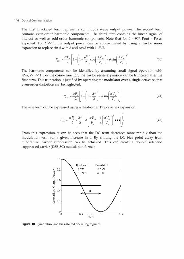
shot noise limit is reached. Consider a MZ-IM biased near = 90º. This corresponds to
an operating regime with reduced output power. For simplicity, let = 90º − δ so that
= 0º corresponds to the quadrature operating point and δ = 0º corresponds to the
transmission null. These operating regimes and angles are summarized graphically in
Figure 10.
By substituting δ for π/2 − , the modulator output power can be written as [40]
1 cos cos sin sin2
in m mout
P V VP
V V
(39)
Optical Communication 146
The first bracketed term represents continuous wave output power. The second term
contains even-order harmonic components. The third term contains the linear signal of
interest as well as odd-order harmonic components. Note that for δ = 90º, Pout = PQ as
expected. For δ << 1, the output power can be approximated by using a Taylor series
expansion to replace sin δ with δ and cos δ with 1- δ2/2.
2
1 1 cos sin2 2
in m mout
P V VP
V V
(40)
The harmonic components can be identified by assuming small signal operation with
πVm/Vπ << 1. For the cosine function, the Taylor series expansion can be truncated after the
first term. This truncation is justified by operating the modulator over a single octave so that
even-order distortion can be neglected.
2
1 1 sin2 2
in mout
P VP
V
(41)
The sine term can be expressed using a third-order Taylor series expansion.
32 1
2 2 6in m m
out
P V VP
V V
(42)
From this expression, it can be seen that the DC term decreases more rapidly than the
modulation term for a given increase in δ. By shifting the DC bias point away from
quadrature, carrier suppression can be achieved. This can create a double sideband
suppressed carrier (DSB-SC) modulation format.
Figure 10. Quadrature and bias-shifted operating regimes.
Photonic Components for Analog Fiber Links 147
6. Passive components for microwave photonics
This section presents an overview of the passive components for microwave photonics such
as optical fiber, optical isolator, polarization control and optical fiber couplers.
6.1. Optical fiber
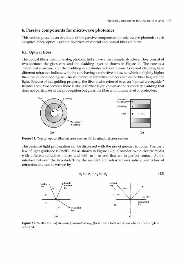
The optical fibers used in analog photonic links have a very simple structure. They consist of
two sections: the glass core and the cladding layer as shown in Figure 11. The core is a
cylindrical structure, and the cladding is a cylinder without a core. Core and cladding have
different refractive indices, with the core having a refractive index, n1, which is slightly higher
than that of the cladding, n2. This difference in refractive indices enables the fiber to guide the
light. Because of this guiding property, the fiber is also referred to as an “optical waveguide.”
Besides these two sections there is also a further layer known as the secondary cladding that
does not participate in the propagation but gives the fiber a minimum level of protection.
Figure 11. Typical optical fiber (a) cross section, (b) longitudinal cross section.
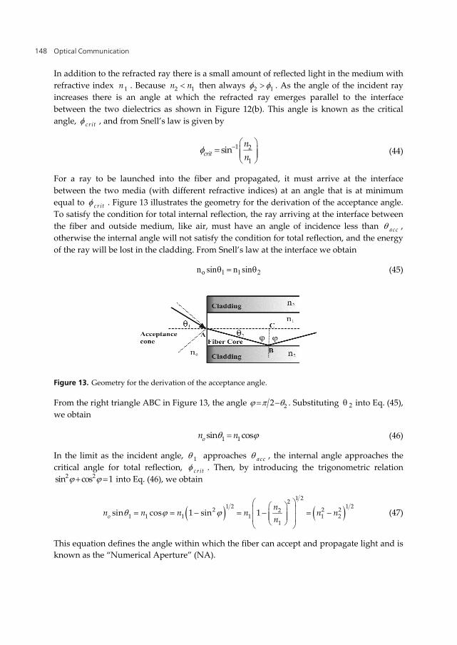
The basics of light propagation can be discussed with the use of geometric optics. The basic
law of light guidance is Snell’s law as shown in Figure 12(a). Consider two dielectric media
with different refractive indices and with n1 > n2 and that are in perfect contact. At the
interface between the two dielectrics, the incident and refracted rays satisfy Snell’s law of
refraction and can be written by
1 1 2 2sin sinn n (43)
Figure 12. Snell’s law, (a) showing transmitted ray, (b) showing total reflection when critical angle is
achieved.
(a) (b)
(a) (b)
Optical Communication 148
In addition to the refracted ray there is a small amount of reflected light in the medium with
refractive index 1n . Because 2 1n n then always 2 1 . As the angle of the incident ray
increases there is an angle at which the refracted ray emerges parallel to the interface
between the two dielectrics as shown in Figure 12(b). This angle is known as the critical
angle, cr it , and from Snell’s law is given by
1 2
1
sincrit
n
n
(44)
For a ray to be launched into the fiber and propagated, it must arrive at the interface
between the two media (with different refractive indices) at an angle that is at minimum
equal to cr it . Figure 13 illustrates the geometry for the derivation of the acceptance angle.
To satisfy the condition for total internal reflection, the ray arriving at the interface between
the fiber and outside medium, like air, must have an angle of incidence less than acc ,
otherwise the internal angle will not satisfy the condition for total reflection, and the energy
of the ray will be lost in the cladding. From Snell’s law at the interface we obtain
211o sinnsinn (45)
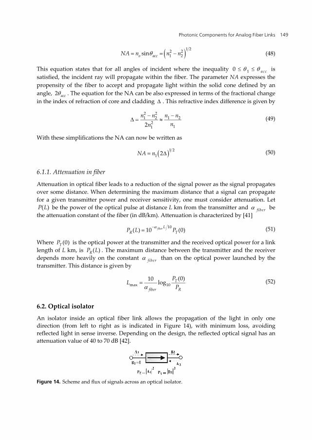
Figure 13. Geometry for the derivation of the acceptance angle.
From the right triangle ABC in Figure 13, the angle 22 . Substituting 2 into Eq. (45),
we obtain
1 1sin coson n (46)
In the limit as the incident angle, 1 approaches acc , the internal angle approaches the
critical angle for total reflection, cr it . Then, by introducing the trigonometric relation 2 2sin cos 1 into Eq. (46), we obtain
1 2
21 2 1 2
2 2 221 1 1 1 1 2
1
sin cos 1 sin 1o
nn n n n n n
n
(47)
This equation defines the angle within which the fiber can accept and propagate light and is
known as the “Numerical Aperture” (NA).
Photonic Components for Analog Fiber Links 149
1 22 21 2sino accNA n n n (48)
This equation states that for all angles of incident where the inequality 10 acc is
satisfied, the incident ray will propagate within the fiber. The parameter NA expresses the
propensity of the fiber to accept and propagate light within the solid cone defined by an
angle, 2 acc . The equation for the NA can be also expressed in terms of the fractional change
in the index of refraction of core and cladding . This refractive index difference is given by
2 21 2 1 2
2112
n n n n
nn
(49)
With these simplifications the NA can now be written as
1 2
1 2NA n (50)
6.1.1. Attenuation in fiber
Attenuation in optical fiber leads to a reduction of the signal power as the signal propagates
over some distance. When determining the maximum distance that a signal can propagate
for a given transmitter power and receiver sensitivity, one must consider attenuation. Let
( )P L be the power of the optical pulse at distance L km from the transmitter and fiber be
the attenuation constant of the fiber (in dB/km). Attenuation is characterized by [41]
10( ) 10 (0)fiber L
R TP L P
(51)
Where (0)TP is the optical power at the transmitter and the received optical power for a link
length of L km, is ( )RP L . The maximum distance between the transmitter and the receiver
depends more heavily on the constant fiber than on the optical power launched by the
transmitter. This distance is given by
max 10
(0)10log T
fiber R
PL
P (52)
6.2. Optical isolator
An isolator inside an optical fiber link allows the propagation of the light in only one
direction (from left to right as is indicated in Figure 14), with minimum loss, avoiding
reflected light in sense inverse. Depending on the design, the reflected optical signal has an
attenuation value of 40 to 70 dB [42].
Figure 14. Scheme and flux of signals across an optical isolator.
Optical Communication 150
The optical isolator is a network of 2 ports, and as such, it can be described by a scattering
matrix 2x2
11 12
21 22
S SS
S S
(53)
This device is characterized by two parameters: the insertion losses (L), and the isolation
relationship (I), both expressed in dB. These parameters are related by the optical power at
the input and the output of the device, the optical fields in their two ports, and their
scattering parameters by means of the following relationships:
2
11
2
21
110 10E
S
SPL Log Log
P S
(54)
2
2
2 2
1 12
110 10
AI Log Log
B S
(55)
In an ideal isolator, insertion losses are L = 0 dB, and the isolation relationship is I .
Generally, optical isolators are placed at the output of the optical sources in order to avoid
reflections of light from returning back to the source avoiding in this way instabilities.
Furthermore, isolators are used by the Doped Fiber Amplifiers with the aim of avoiding an
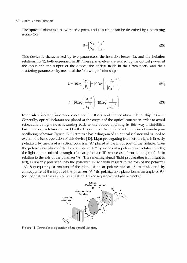
oscillating behavior. Figure 15 illustrates a basic diagram of an optical isolator and is used to
explain the basic operation of this device [43]. Light propagating from left to right is linearly
polarized by means of a vertical polarizer "A" placed at the input port of the isolator. Then
the polarization plane of the light is rotated 45° by means of a polarization rotator. Finally,
the light is transmitted through a linear polarizer "B" whose axis forms an angle of 45° in
relation to the axis of the polarizer "A". The reflecting signal (light propagating from right to
left), is linearly polarized into the polarizer "B" 45° with respect to the axis of the polarizer
"A". Subsequently, a rotation of the plane of linear polarization at 45° is made, and by
consequence at the input of the polarizer "A," its polarization plane forms an angle of 90°
(orthogonal) with its axis of polarization. By consequence, the light is blocked.
Figure 15. Principle of operation of an optical isolator.
Photonic Components for Analog Fiber Links 151
6.3. Polarization rotator
A polarization rotator rotates the polarization plane of an optical field linearly polarized at
its input at an angle [43]. If the input signal is an optical field linearly polarized forming
an angle 1 with the axis x, then the Jones Matrix can be expressed as
1
1
cos
sinJ
(56)
The output signal is an optical field linearly polarized forming an angle 2 , and by
consequence the Jones matrix corresponding to the rotator is given as
cos sin
sin cosM
(57)
where: 2 1 .
6.4. Polarization control
A polarization control changes the polarization state of the light. Currently in the systems,
the polarization controls can be inserted in the arms of an optical signal or in the arms of a
signal of an optical local oscillator in order to maintain or to match the polarization state of
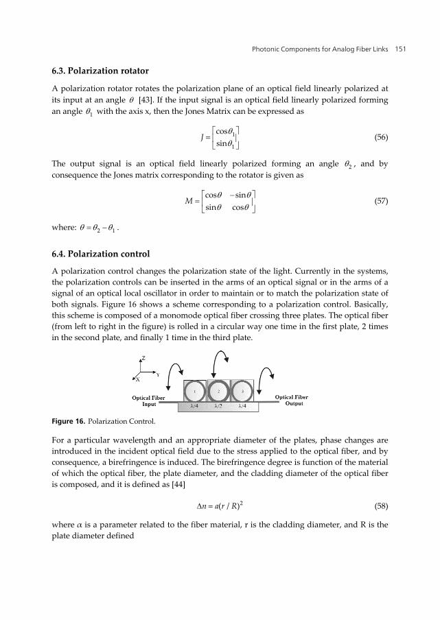
both signals. Figure 16 shows a scheme corresponding to a polarization control. Basically,
this scheme is composed of a monomode optical fiber crossing three plates. The optical fiber
(from left to right in the figure) is rolled in a circular way one time in the first plate, 2 times
in the second plate, and finally 1 time in the third plate.
Figure 16. Polarization Control.
For a particular wavelength and an appropriate diameter of the plates, phase changes are
introduced in the incident optical field due to the stress applied to the optical fiber, and by
consequence, a birefringence is induced. The birefringence degree is function of the material
of which the optical fiber, the plate diameter, and the cladding diameter of the optical fiber
is composed, and it is defined as [44]
2( / )n a r R (58)
where α is a parameter related to the fiber material, r is the cladding diameter, and R is the
plate diameter defined

Optical Communication 152
28 /R ar (59)
When an optical field is propagated by the fiber control, this field will suffer a phase change
of 90° at the output of the first plate, and by consequence this plate has a similar behavior
as a retarder plate of /4 [44]. The second plate acts as a retarder plate of /2 because at
the output the optical field has a phase change of 180° This phase change can be expressed
as [44].
(2 / ) 2n R (60)
Taking into account this effect and assuming that the incident optical field has an elliptical
polarization state, the first retarder plate /4 changes this polarization state to a lineal
polarization state. The second retarder plate /2 rotates the polarization state toward a
specific direction. Finally, the third plate /4 changes the linear polarization into a desired
polarization state.
6.5. Optical fiber couplers
The optical system communications requires devices capable of coupling light from one
fiber or various fibers to others. Typically, this coupling of light has been achieved by using
beam splitters fabricated on bulk devices. However, for the case of guided signal
transmission this task can be achieved by using couplers [45]. A coupler is a passive device
capable of distributing energy from M input guides to N output guides [45]. In this sense,
two technologies have been developed to fabricate couplers. One of these is based on optical
fibers whereas the other is based on bulk optics, however the principles of operation are
similar in both cases. Currently, the coupler most commonly used in optical system
communications is the directional coupler 2x2. Figure 17 illustrates a scheme of this type of
coupler.
Figure 17. Scheme of an optical coupler 2x2.
From this figure, it is clearly appreciable that this is a 4-port device. In technology of optical
fibers, this device can be of two types: (a) Evanescent field [46, 47], and (b) Modal
interference. In the first case, the evanescent mode corresponding to the fundamental mode
of a guide is used to excite the apparition and propagation of the fundamental mode in
another guide producing a controllable energy. In the second case, a common bimodal zone
to both guides is generated obtaining in this way the transfer of energy by means of a
controlled interference between the modes that are being propagated in this zone. The
coupler of evanescent field is generated by placing two guides very near between them as is
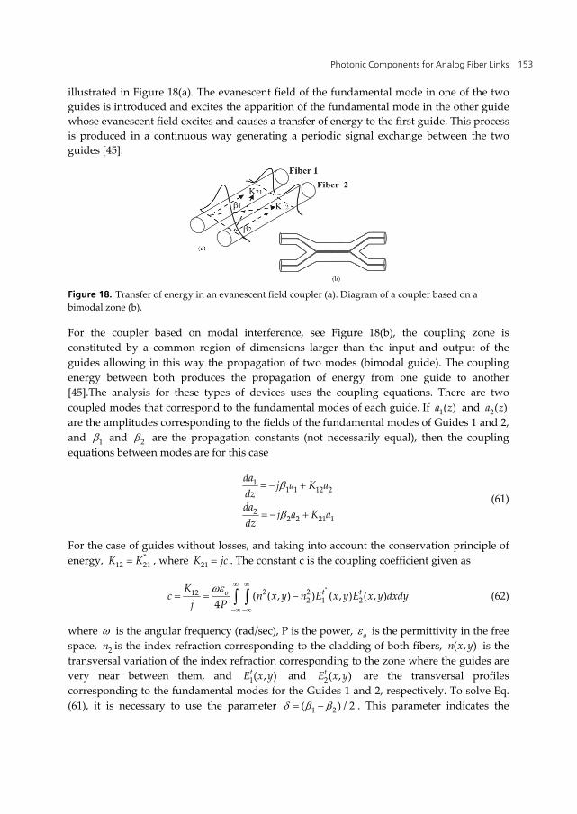
Photonic Components for Analog Fiber Links 153
illustrated in Figure 18(a). The evanescent field of the fundamental mode in one of the two
guides is introduced and excites the apparition of the fundamental mode in the other guide
whose evanescent field excites and causes a transfer of energy to the first guide. This process
is produced in a continuous way generating a periodic signal exchange between the two
guides [45].
Figure 18. Transfer of energy in an evanescent field coupler (a). Diagram of a coupler based on a
bimodal zone (b).
For the coupler based on modal interference, see Figure 18(b), the coupling zone is
constituted by a common region of dimensions larger than the input and output of the
guides allowing in this way the propagation of two modes (bimodal guide). The coupling
energy between both produces the propagation of energy from one guide to another
[45].The analysis for these types of devices uses the coupling equations. There are two
coupled modes that correspond to the fundamental modes of each guide. If 1( )a z and 2( )a z
are the amplitudes corresponding to the fields of the fundamental modes of Guides 1 and 2,
and 1 and 2 are the propagation constants (not necessarily equal), then the coupling
equations between modes are for this case
11 1 12 2
22 2 21 1
daj a K a
dzda
j a K adz
(61)
For the case of guides without losses, and taking into account the conservation principle of
energy, *12 21K K , where 21K jc . The constant c is the coupling coefficient given as
*2 212
2 1 2( ( , ) ) ( , ) ( , )4
t toKc n x y n E x y E x y dxdy
j P
(62)
where is the angular frequency (rad/sec), P is the power, o is the permittivity in the free
space, 2n is the index refraction corresponding to the cladding of both fibers, ( , )n x y is the
transversal variation of the index refraction corresponding to the zone where the guides are
very near between them, and 1( , )tE x y and 2( , )tE x y are the transversal profiles
corresponding to the fundamental modes for the Guides 1 and 2, respectively. To solve Eq.
(61), it is necessary to use the parameter 1 2( ) / 2 . This parameter indicates the
Optical Communication 154
difference between the guides that composes the coupler. The solution of (61) provides the
values of the amplitudes of the electric field in any point z for both guides 1( )a z and 2( )a z
in function of the values of the amplitudes of electric fields to its input 1(0)a and 2(0)a . The
solution can be expressed as a matrix [45]
1 2
21 1* *
2 2
( ) (0)
( ) (0)
j A jBa z ae
a z aJB A
(63)
Where
2 2
2 2
2 2
2 2
2 2
cossen z c
A z c jc
sen z cB c
c
(64)
The phase factor 1 2exp2
j
is a common factor, and so it is not necessary to be
considered in subsequent calculations. In practice, optical fiber couplers are made using similar
fibers, for this reason 1 2 and 0 . Consequently, the matrix relationship (63) is
1 1
2 2
cos ( )( ) (0)
( ) (0)( ) cos( )
cz jsen cza z a
a z ajsen cz cz
(65)
Defining the coupling constant as 2( )k sen cz , then (65) takes the form
1 1
2 2
( ) (0)1
( ) (0)1
a z ak j k
a z aj k k
(66)
Since the coupling constant k is generally variable with wavelength, the characteristics of the
coupler may vary with the operating frequency. However, this effect can be utilized to create
optical filters, multiplexers and wavelength demultiplexers [45]. The energy transfer process
can easily be evaluated assuming that at the input of the coupler there is only signal in Guide
1, this is, 2(0) 0a . From equation (65) it is possible to obtain the optical power in each guide
for each value of z:
2 21 1 1 1
2 22 2 1 1
( ) ( ) (0)cos ( ) (0)(1 )
( ) ( ) (0) ( ) (0)
P z a z P cz P k
P z a z P sen cz P k
(67)
A special case is when 1 / 2k . In this case, the optical power in the input guide is divided
equally between the two output guides of the coupler. The device is then called a 3 dB
coupler.
Photonic Components for Analog Fiber Links 155
Until now, the description of the coupler has been made on the assumption that it behaves
ideally, this is, without considering losses. In practice this is not real, and from experimental
as well as commercial points of view, it is necessary to define a set of parameters that allows
the behavior of the coupler to be determined.
Coupling constant
4
3 4
Pk
P P
(68)
This constant indicates the optical power division between the output ports.
Excess Loss
1
3 4
( ) 10log( ) 10P
dB LogP P
(69)
This parameter provides the relationship between the total power at the input and the
output power of the device.
Directivity coupler
2
1
( ) 10P
D dB LogP
(70)
This parameter indicates the fraction of input power that the coupler returns in the form of
signal retro-propagated to Guide 2.
Insertion Losses
1
3
( ) 10i
PL dB Log
P
(71)
This parameter indicates the level of losses introduced by the coupler considering that the
signal propagation is through a given configuration of the input port and the output port.
7. Experimental results
According to the theoretical descriptions explained in this chapter, we have assembled in
the laboratory the proposed experimental setup shown in Figure 1. For the stage where
relaxation oscillation frequencies were measured, we used two fiber-coupled DFB laser
sources (Thorlabs, model S3FC1550) with a central wavelength of 1550 nm, a threshold
current of 8 mA and a differential responsivity of 0.25 mW/mA. An optical isolator OI was
connected to each DFB laser to avoid instabilities from feedback into the lasers, and an
optical coupler was used to split the optical beam. In order to increase the power level of the
microwave signal, it was necessary to connect an EDFA in one of the ports of the optical
Optical Communication 156
coupler. After that, the amplified optical signal was launched to fast photodetector PD1
(MITEQ model DR-125G-A) which has a typical optical-to-electrical transfer gain (V/W) of
1900, and –3 dB bandwidth of 12.5 GHz. In order to measure the optical spectrum of the
DFB laser, it was necessary to connect the other port of optical coupler to an OSA Anritsu
model MS9710C. On the other hand, the obtained photo-current by photo-detector was
measured by using an ESA, Agilent model E4407B.
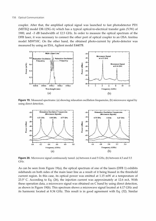
Figure 19. Measured spectrums: (a) showing relaxation oscillation frequencies, (b) microwave signal by
using direct detection.
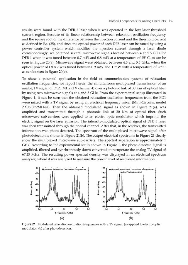
Figure 20. Microwave signal continuously tuned. (a) between 4 and 5 GHz, (b) between 4.5 and 5.5
GHz.
As can be seen from Figure 19(a), the optical spectrum of one of the lasers (DFB 1) exhibits
sidebands on both sides of the main laser line as a result of it being biased in the threshold
current region. In this case, its optical power was emitted at 1.15 mW at a temperature of
23.5º C. According to Eq. (26), the injection current was approximately at 12.6 mA. With
these operation data, a microwave signal was obtained on C band by using direct detection,
as shown in Figure 19(b). This spectrum shows a microwave signal located at 4.17 GHz and
its harmonic located at 8.34 GHz. This result is in good agreement with Eq. (32). Similar
(a) (b)
(a) (b)
Photonic Components for Analog Fiber Links 157
results were found with the DFB 2 laser when it was operated in the low laser threshold
current region. Because of its linear relationship between relaxation oscillation frequency
and the square root of the difference between the injection current and the threshold current
as defined in Eq. (25), and since the optical power of each DFB laser can be tuned by using a
power controller system which modifies the injection current through a laser diode
correspondingly, we obtained several microwave signals located between 4 and 5 GHz for
DFB 1 when it was tuned between 0.7 mW and 0.8 mW at a temperature of 25º C, as can be
seen in Figure 20(a). Microwave signal were obtained between 4.5 and 5.5 GHz, when the
optical power of DFB 2 was tuned between 0.9 mW and 1 mW with a temperature of 26º C
as can be seen in figure 20(b).
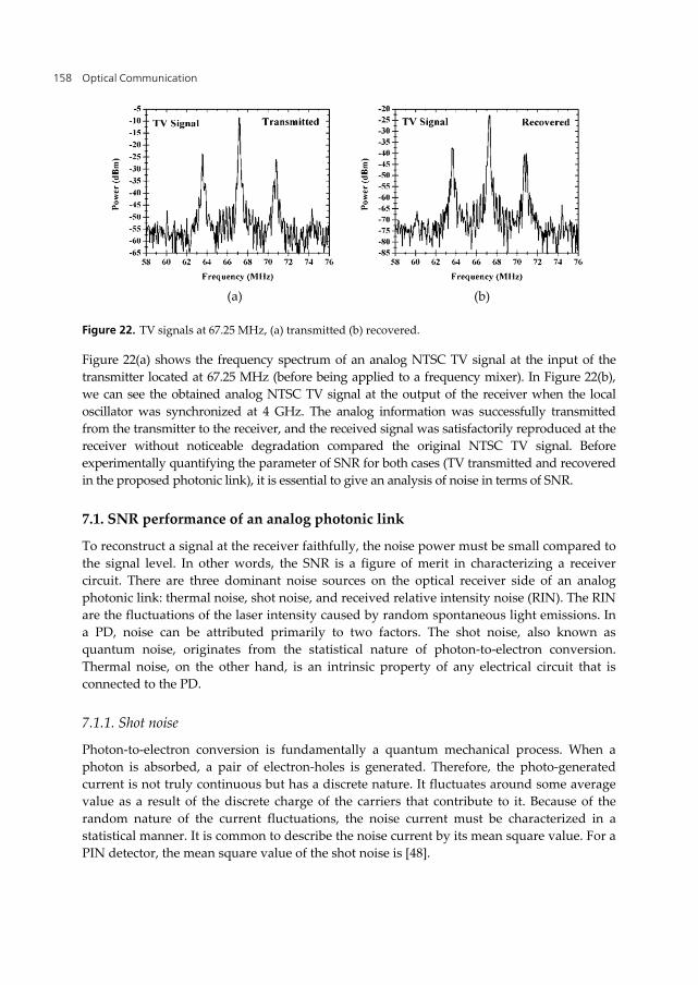
To show a potential application in the field of communication systems of relaxation
oscillation frequencies, we report herein the simultaneous multiplexed transmission of an
analog TV signal of 67.25 MHz (TV channel 4) over a photonic link of 30 Km of optical fiber
by using two microwave signals at 4 and 5 GHz. From the experimental setup illustrated in
Figure 1, it can be seen that the obtained relaxation oscillation frequencies from the PD1
were mixed with a TV signal by using an electrical frequency mixer (Mini-Circuits, model
ZX05-U72MH-s+). Then the obtained modulated signal as shown in Figure 21(a), was
amplified and transmitted through a photonic link of 30 Km of optical fiber. Such
microwave sub-carriers were applied to an electro-optic modulator which imprints the
electric signal on the laser emission. The intensity-modulated optical signal of DFB 3 laser
was then transmitted through the optical channel. After that, in the receiver, the transmitted
information was photo-detected. The spectrum of the multiplexed microwave signal after
photodetection is shown in Figure 21(b). The output electrical spectrums in Figure 21 clearly
show the multiplexed microwave sub-carriers. The spectral separation is approximately 1
GHz. According to the experimental setup shown in Figure 1, the photo-detected signal is
amplified, filtered and synchronously down-converted to recuperate the analog TV signal of
67.25 MHz. The resulting power spectral density was displayed in an electrical spectrum
analyzer, where it was analyzed to measure the power level of recovered information.
Figure 21. Modulated relaxation oscillation frequencies with a TV signal. (a) applied to electro-optic
modulator, (b) after photodetection.
(a) (b)
Optical Communication 158
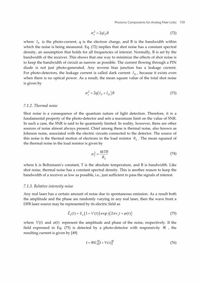
Figure 22. TV signals at 67.25 MHz, (a) transmitted (b) recovered.
Figure 22(a) shows the frequency spectrum of an analog NTSC TV signal at the input of the
transmitter located at 67.25 MHz (before being applied to a frequency mixer). In Figure 22(b),
we can see the obtained analog NTSC TV signal at the output of the receiver when the local
oscillator was synchronized at 4 GHz. The analog information was successfully transmitted
from the transmitter to the receiver, and the received signal was satisfactorily reproduced at the
receiver without noticeable degradation compared the original NTSC TV signal. Before
experimentally quantifying the parameter of SNR for both cases (TV transmitted and recovered
in the proposed photonic link), it is essential to give an analysis of noise in terms of SNR.
7.1. SNR performance of an analog photonic link
To reconstruct a signal at the receiver faithfully, the noise power must be small compared to
the signal level. In other words, the SNR is a figure of merit in characterizing a receiver
circuit. There are three dominant noise sources on the optical receiver side of an analog
photonic link: thermal noise, shot noise, and received relative intensity noise (RIN). The RIN
are the fluctuations of the laser intensity caused by random spontaneous light emissions. In
a PD, noise can be attributed primarily to two factors. The shot noise, also known as
quantum noise, originates from the statistical nature of photon-to-electron conversion.
Thermal noise, on the other hand, is an intrinsic property of any electrical circuit that is
connected to the PD.
7.1.1. Shot noise
Photon-to-electron conversion is fundamentally a quantum mechanical process. When a
photon is absorbed, a pair of electron-holes is generated. Therefore, the photo-generated
current is not truly continuous but has a discrete nature. It fluctuates around some average
value as a result of the discrete charge of the carriers that contribute to it. Because of the
random nature of the current fluctuations, the noise current must be characterized in a
statistical manner. It is common to describe the noise current by its mean square value. For a
PIN detector, the mean square value of the shot noise is [48].
(a) (b)
Photonic Components for Analog Fiber Links 159
2 2s PqI B (72)
where PI is the photo-current, q is the electron charge, and B is the bandwidth within
which the noise is being measured. Eq. (72) implies that shot noise has a constant spectral
density, an assumption that holds for all frequencies of interest. Normally, B is set by the
bandwidth of the receiver. This shows that one way to minimize the effects of shot noise is
to keep the bandwidth of circuit as narrow as possible. The current flowing through a PIN
diode is not just photo-generated. Any reverse bias junction has a leakage current.
For photo-detectors, the leakage current is called dark current DI , because it exists even
when there is no optical power. As a result, the mean square value of the total shot noise
is given by
2 2s P Dq I I B (73)
7.1.2. Thermal noise
Shot noise is a consequence of the quantum nature of light detection. Therefore, it is a
fundamental property of the photo-detector and sets a maximum limit on the value of SNR.
In such a case, the SNR is said to be quantumly limited. In reality, however, there are other
sources of noise almost always present. Chief among these is thermal noise, also known as
Johnson noise, associated with the electric circuits connected to the detector. The source of
this noise is the thermal motion of electrons in the load resistor LR . The mean squared of
the thermal noise in the load resistor is given by
2 4T
L
kTB
R (74)
where k is Boltzmann’s constant, T is the absolute temperature, and B is bandwidth. Like
shot noise, thermal noise has a constant spectral density. This is another reason to keep the
bandwidth of a receiver as low as possible, i.e., just sufficient to pass the signals of interest.
7.1.3. Relative intensity noise
Any real laser has a certain amount of noise due to spontaneous emission. As a result both
the amplitude and the phase are randomly varying in any real laser, then the wave front a
DFB laser source may be represented by its electric field as
1( ) 1 ( ) exp 2 ( )o oE t E V t j t t
(75)
where ( )V t and ( )t represent the amplitude and phase of the noise, respectively. If the
field expressed in Eq. (75) is detected by a photo-detector with responsivity , the
resulting current is given by [49]
22o )t(V1EI (76)
Optical Communication 160
Typically, the amplitude noise, ( )V t , is very small so that Eq (76) can be rewritten as
)t(V21EI 2o (77)
The noise term 2 ( )V t represents the RIN; it describes the laser power fluctuations. The
power spectral density of the RIN is denoted by ; it has the units of 1/Hz. The quantity
log10 is known as the RIN.
10 log ,R IN dB/Hz (78)
The typical values of RIN for a DFB laser are better than -155 dB/Hz. The power spectrum of
the RIN is not flat, hence it is not a white noise source. In an analog photonic link, we use a
photodiode to detect the optical power from the M-Z modulator. Thus, RIN can be
expressed as [50].
2D
2RIND
2D
2RIND
BI
i
IB
i
RIN
(79)
From Eq. (79), we obtain the received mean square current RIN noise of the receiver as:
BIRINi 2D
2RIND (80)
Comparatively, 2RINDi is proportional to 2
DI , whereas the shot noise is linearly proportional
to DI . Therefore, the RIN noise will tend to be the dominant noise, when the laser average
power is increasing.
7.1.4. Signal-to-Noise Ratio (SNR)
Once we have characterized the noise level at the input of a receiver, it is possible to analyze
the SNR. The SNR is an important parameter because it determines the performance of a
receiver. In analog receivers, SNR is the main figure of merit and characterizes the quality of
the analog link. Assuming that all of the noise sources described previously are
uncorrelated, the signal-noise ratio of the link at the single photo-detector can be expressed
by:
BIRIN
R
kTB4B)II(q2
P
i
PSNR
2D
LDP
2R
2
2RIND
2T
2s
2R
2
(81)
From Eq. (81), RP is the received optical power at the end of the optical link. On the other
hand, according to the Figure 9 and Eq. (42), and considering that the modulated optical
power at the output of MZ-IM is propagated through an optical fiber of length L, the RP can
be written by / 10
10 fiber L
R ou tP P
. Here fiber is the optical fiber loss, and L is the

Photonic Components for Analog Fiber Links 161
transmission distance of the optical fiber. In that case if we consider that πVm/Vπ << 1 then
Eq (81), can be rewritten as
22
/1022/102
2 2
1010 2 2
4 42 ( ) 2 ( )
fiberfiber
L in mL
out
P D D P D DL L
P VP V
SNRkTB kTB
q I I B RIN I B q I I B RIN I BR R
(82)
This equation provides several insights into the SNR behavior of a receiver. Notice that as
expected, increasing the optical power Pin increases the SNR. On the other hand, increasing
the bandwidth of the receiver, B, reduces the SNR. The denominator of Eq. (82) shows the
contribution of thermal noise, shot noise and RIN to SNR. An interesting point is that as LR
increases, the effects of thermal noise decrease. In a practical circuit, however, LR cannot be
increased too much because it will reduce the bias headroom of the photo-detector.
7.1.5. Experimental (SNR)
In order to measure the quality of the received signal, it was necessary to experimentally
quantify the parameter of signal-to-noise ratio (SNR) for both cases (TV transmitted and
recovered in the photonic link).
Figure 23. TV signals at 67.25 MHz in order to measure experimentally the SNR parameter, (a)
transmitted (b) recovered.
As can be seen from figure 23(a), the SNR measured in a bandwidth of 6 MHz was of
52.67 dB. On the other hand the SNR measured in the receiver was of 46.5 dB as shown in
figure 23(b). Notice that the SNR measured in the receiver was degraded by 6.17 dB due to
the optical fiber loss and it could be improved substantially with the addition of another
stage of electrical amplification at the end of the link. However, values of SNR > 45 dB
(a) (b)
Optical Communication 162
ensure a good quality of images [51]. The differential gain and differential phase were not
measured in this chapter. Nevertheless we have experimentally demonstrated that the
generated microwave signal (relaxation oscillation frequency) by using direct detection can
be used as information carriers in a multiplexed transmission system based in an analog
photonic link and we have used a TV signal of test to verify it.
8. Conclusions
In this chapter we have described optical components used in the proposed experimental
setup, as well as, we have experimentally demonstrated that two DFB lasers biased in the low
laser threshold current region showed relaxation oscillation frequencies in the laser intensity.
These frequencies were seen as sidebands on both sides of the main laser line when the
optical spectrum was analyzed with a spectrum analyzer. This result allowed the generation
of microwave signals on C band by using the operation principle of direct detection. Along
with the proposed experimental setup in this work, an analog NTSC TV signal was
simultaneously transmitted in an analog photonic link by using relaxation oscillation
frequency as information carriers located at 4 and 5 GHz. The TV signal was received
satisfactorily when the local oscillators were synchronized in the receiver. For our proposed
experimental setup to be recovered the transmitted information successfully, it was necessary
to have additional amplifiers which adapt the power levels, improving the quality of the
signals. The results obtained in this work ensure that as an interesting alternative, several
modulation schemes can be used for transmitting not only analog information but also digital
information by using relaxation oscillation frequencies as information carriers. The proposed
experimental setup described here can generate continually tuned microwaves. In addition,
we can use this feature to transmit several TV signals using frequency division multiplexing
schemes (FDM) and wavelength division multiplexing (WDM) techniques, not only point to
point but also by using bidirectional systems, exploiting the use of mature microwave signal
processing techniques, where multiple signals are multiplexed in the microwave domain and
transmitted by a single optical carrier when subcarrier multiplexing (SCM) schemes are
proposed. To the best of our knowledge, this is the first published work on the employ of
relaxation oscillation frequencies as information carriers for transmitting analog TV signals
on a long distance photonic link. In addition, as an alternative of analog photonic links, our
proposal shows outstanding performance.
Author details
Alejandro García Juárez
University of Sonora, Department of Physics Research, Mexico
Ignacio Enrique Zaldívar Huerta
National Institute of Astrophysics, Optics and Electronics. Department of Electronics, Mexico
Jorge Rodríguez Asomoza
University of the Americas-Puebla, Department of Electronics, Mexico
Photonic Components for Analog Fiber Links 163
María del Rocío Gómez Colín
University of Sonora, Department of Physics, Mexico
Acknowledgement
This work was supported by The Mexican Consejo Nacional de Ciencia y Tecnología
(CONACyT), (grant No 102046).
9. References
[1] Kai Wang, Xiaoping Zheng, Hanyi Zhang, and Yili Guo. A Radio-Over-Fiber
Downstream Link Employing Carrier-Suppressed Modulation Scheme to Regenerate
and Transmit Vector Signals. IEEE Photonics Technology Letters 2007; vol. 19, no. 18,
pp. 1365-1367.
[2] D. Novak, A. Nirmalathas, C. Lim, C. Marra, and R. B. Waterhouse. Fiber-radio-
challenges and possible solutions. Topical Meeting Microwave Photonics 2003, Sep. 10–
12, (2003).
[3] X. Zhang, B. Liu, J. Yao, K. Wu, and R. Kashyap. A novel millimeter-wave-band radio-
over-fiber system with dense wavelength-division multiplexing bus architecture. IEEE
Transactions on Microwave Theory and Techniques 2006; vol. 54, no. 2, pp. 929–937.
[4] Stavros Iezekiel. Microwave Photonics Devices and Applications. John Wiley; 2009.
[5] Xue Jun Meng. A Dispersion Tolerant Analog Optical Receiver for Directly Modulated
RF Photonic Links. IEEE Photonics Technology Letters 2007; vol. 19, no. 6, march 15
[6] Spiros Mikroulis, Sotiris Karabetsos, Evaggelos Pikasis, Aristidis Chipouras and
Athanase Nassiopoulos. Evaluation on the performance of Distributed Feedback Lasers
(DFB) for Radio-Over-Fiber (RoF) Applications. International Conference on
Telecommunications & multimedia, Greece 2006.
[7] A. Baylón-Fuentes, P. Hernández-Nava, A.García-Juárez, I. E. Zaldívar-Huerta, J.
Rodríguez-Asomoza, G. Aguayo-Rodríguez and R. Gómez-Colín. Modulation of
Relaxation Oscillation Frequency of a DFB Laser by Using Direct Detection. Broadband
Access Communications Technologies V, Proc. of SPIE Vol. 7958, 2011.
[8] A.J. Seeds. Broadband wireless access using millimetre-wave over fibre systems. IEEE
MTTS Int. Microwave Symp.1997; vol.1, pp. 23-25.
[9] W.H. Loh, C.L. Tang. Polarization modulation for optical-microwave applications in
phased array antennas. IEEE Photonics Technology Letters 1991; vol.3 no. 5 pp. 478-480.
[10] J.J. O’Reilly, P.M. Lane. Fibre-supported optical generation and delivery of 60 GHz
signals. Electronics Letters 1994; vol. 30, no. 16, pp. 1329-1330.
[11] D.C. Scott, D.V. Plant, H.R. Fetterman. 60 GHz sources using optically driven
heterojunction bipolar transistors. Applied Physics Letters 1992; vol. 61, no. 1, pp. 1-3.
[12] J.B. Georges, M. -H. Kiang, K. Heppell, M. Sayed, K.Y. Lau. Optical Transmission of
Narrow-Band Millimeter Wave Signals by Resonant Modulation of Monolithic
Semiconductor Lasers. IEEE Photonics Technology Letters 1994; vol. 6 no. 4 pp 568-570.
Optical Communication 164
[13] C.R. Lima, D. Wake, P.A. Davis. Compact optical millimetre-wave source using a dual-
mode semiconductor laser. Electronics Letters 1995; vol. 31 no. 5, pp. 364-366.
[14] L. Goldberg, A.M. Yurek, H.F. Taylor, J.F. Weller. 35 GHz microwave signal generation
with an injection-locked laser diode. Electronics Letters 1985; vol. 21, no. 18, pp. 814-
815.
[15] P. Shen, N.J. Gomes, P.A. Davis, W.P. Shillue, P.G. Huggard, B.N. Ellison, in: Proc. Int.
Top. Microw. Photon. Metting, 2003.
[16] D. Wake, C.R. Lima, P.A. Davies. Optical generation of millimeter-wave signals for
fiber-radio systems using a dual-mode DFB semiconductor laser. IEEE Transaction on
Microwave Theory and Techniques 1995; vol. 43, no. 9, pp. 2270 – 2276.
[17] R.T. Ramos, A.J. Seeds. Fast heterodyne optical phase-lock loop using double quantum
well laser diodes. Electronics Letters 1992; vol. 28 no. 1, pp 82-83.
[18] A. García-Juárez, I. E. Zaldívar-Huerta, G. Aguayo-Rodríguez, J. Rodríguez-Asomoza,
R. Gómez-Colín, A. Vera-Marquina, M. C. Acosta-Enriquez, A. Rojas-Hernández.
Optical heterodyne technique for generating and distributing microwave signals.
Broadband Access Communications Technologies IV, Proc. of SPIE Vol. 7620, 2010.
[19] A. García-Juárez, I. E. Zaldívar-Huerta, G. Aguayo-Rodríguez, J. Rodríguez-Asomoza,
R.Gómez-Colín, A. Rojas-Hernández. Coherent demodulation of microwave signals by
using optical heterodyne technique with applications to point to point indoor wireless
communications systems. 2011 J. Phys.: Conf. Ser. 274 012008, doi:10.1088/1742-
6596/274/1/012008. (http://iopscience.iop.org/1742-6596/274/1/012008)
[20] Jianping Yao. Microwave Photonics. Journal of Lightwave Technology 2009; vol. 27, no.
3, pp. 314-335.
[21] L. Goldberg, H. F. Taylor, J. F. Weller, and D. M. Bloom. Microwave signal generation
with injection locked laser diodes. Electron. Letters 1983; vol. 19, no. 13, pp. 491-493.
[22] U. Gliese, T. N. Nielsen, M. Bruun, E. L. Christensen, K. E. Stubkjaer, S. Lindgren, and B.
Broberg. A wideband heterodyne optical phaselocked loop for generation of 3–18 GHz
microwave carriers. IEEE Photon. Technol. Letters 1992; vol. 4, no. 8, pp. 936–938.
[23] A. C. Bordonalli, C.Walton, and A. J. Seeds. High-Performance phase locking of wide
linewidth semiconductor lasers by combined use of optical injection locking and optical
phase-lock loop. J. Lightwave Technology 1999; vol. 17, no. 2, pp. 328–342.
[24] Z. F. Fan and M. Dagenais. Optical generation of a mHz-linewidth microwave signal
using semiconductor lasers and a discriminator-aided phase-locked loop. IEEE Trans.
Microw. Theory Tech., 1997; vol. 45, no. 8, pp. 1296–1300.
[25] J. J. O’Reilly, P. M. Lane, R. Heidemann, and R. Hofstetter. Optical generation of very
narrow linewidth millimeter wave signals. Electron. Letters 1992; vol. 28, no. 25, pp.
2309–2311.
[26] J. J. O’Reilly and P. M. Lane. Remote delivery of video services using mm-wave and
optics. J. Lightw. Technol. 1994; vol. 12, no. 2, pp. 369–375.
[27] P. Shen, N. J. Gomes, P. A. Davies, W. P. Shillue, P. G. Huggard, and B. N. Ellison.
High-purity millimeter-wave photonic local oscillator generation and delivery. in Proc.
Int. Microw. Photonics Topical Meeting, Sep. 10–12, 2003, pp. 189–192.
Photonic Components for Analog Fiber Links 165
[28] G. Qi, J. P. Yao, J. Seregelyi, C. Bélisle, and S. Paquet. Generation and distribution of a
wide-band continuously tunable mm-wave signal with an optical external modulation
technique. IEEE Trans. Microw. Theory Tech. 2005; vol. 53, no. 10, pp. 3090–3097.
[29] X. Chen, Z. Deng, and J. P. Yao. Photonic generation of microwave signal using a dual-
wavelength single-longitudinal-mode fiber ring laser. IEEE Trans. Microw. Theory
Tech. 2006; vol. 54, no. 2, pp. 804–809.
[30] X. Chen, J. P. Yao, and Z. Deng. Ultranarrow dual-transmission-band fiber Bragg
grating filter and its application in a dual-wavelength single-longitudinal-mode fiber
ring laser. Opt. Lett. 2005; vol. 30, no. 16, pp. 2068–2070.
[31] H. Zandi, M. Bavafa, M. Chamanzar, and S. Khorasani. Analysis of power harmonic
content and relaxation resonant frequency of a diode laser. Proc. SPIE, Vol. 6468, No.
64680J, 2007.
[32] H. Zandi, M. Bavafa, M.R. Chamanzar and S. Khorasani. Harmonic Content and
Relaxation Resonant Frequency of a Modulated Laser Diode. Transactions D: Computer
Science & Engineering and Electrical Engineering 2009; Vol. 16, No. 2, pp. 145-156.
[33] M. Bavafa, H. Zandi, M. Chamanzar, and S. Khorasani. Optimal Operation Point for the
Primary Harmonic Content of a Modulated Laser Diode. Proceedings of the 6th WSEAS
International Conference on Microelectronics, Nanoelectronics, Optoelectronics,
Istanbul, Turkey, May 27-29, 2007.
[34] L.A. Coldren, and S.W Corzine. Diode Lasers and Photonic Integrated Circuits. John
Wiley & Sons; 1995.
[35] B. E. A. Saleh. Fundamentals of Photonics. John Wiley & Sons, Inc; 1991. pp. 624-626.
[36] A. Baylón-Fuentes, P. Hernández-Nava, A.García-Juárez, I. E. Zaldívar-Huerta, J.
Rodríguez-Asomoza, G. Aguayo-Rodríguez and R. Gómez-Colín. Modulation of
Relaxation Oscillation Frequency of a DFB Laser by Using Direct Detection. Broadband
Access Communications Technologies V, Proc. of SPIE Vol. 7958, 2011.
[37] A.García-Juárez, I. E. Zaldívar-Huerta, J. Rodríguez-Asomoza3, R. Gómez-Colín, A.G
Rojas-Hernández, D. Berman-Mendoza, R. Gómez-Fuentes and A. Vera Marquina.
Analog Photonic Link by Using DFB lasers Operated in the Low Laser Threshold
Current Region and External Modulation. Broadband Access Communications
Technologies VI, Proc. of SPIE Vol. 8282, 2012.
[38] D. Derickson. Fiber Optic Test and Measurement. Prentice Hall PTR; 1998. pp. 175-179.
[39] C. H. Cox. Analog Optical Links: Theory and Practice. Cambridge: Cambridge
University Press; 2004, pp. 37–38.
[40] X. Jun Meng, A. Karim. Microwave Photonic Link with Carrier Suppression for
Increased Dynamic Range. Fiber and Integrated Optics, Taylor & Francis Group; 2006.
pp. 161- 174.
[41] P. S. Henry. Lightwave primer,” IEEE J. Quantum Electron. 1985; vol. QE-21, pp. 1862–
1879.
[42] Jha, A.R. State of the Art Fiber Optic Components and Photonic Devices for Optical
Communication and High Speed Transmission. 31st European Microwave Conference,
2001.
[43] B. E. A. Saleh. Fundamentals of Photonics. John Wiley & Sons, Inc; 1991. pp. 193-237
Optical Communication 166
[44] Donald K. Wilson. Polarization control aids fiber component testing. Lasers Focus
World 1997; pp. 129 –133.
[45] José Capmany, F. Javier Fraile-Peláez y Javier Martí. Dispositivos de Comunicaciones
Ópticas. Editorial Síntesis.
[46] R. A. Bergh, G. Kotler y H. J Shaw. Electron. Lett. , 1980; p 260.
[47] S. K. Sheem y T. Giallorentzi. Opt. Lett. 1979; p 29.
[48] E. Garmire. Sources, modulation, and detectors for fiber-optic communication systems,
in Fiber Optics, Handbook. Edited by M. Bass, McGraw-Hill, New York; 2002 pp. 4.1–
4.78,
[49] Leonid Kazovsky, Sergio Benedetto and Alan Willner. Optical Communications
Systems, Artech House; 1996.
[50] Abhay Joshi, Xinde Wang, Dan Mohr, Don Becker, and Christoph Wree. Balanced
photoreceivers for analog and digital fiber optic communications. Proc. of SPIE Vol.
5814, 2005.
[51] M. Kowalczyk and J. Siuzdak. Multi-channel am video transmission beyond the
baseband of multimode fiber. Microwave and optical technology letters 2010; vol. 52,
no. 2, pp. 435-438.